a wireless mri system using millimeter wave …
TRANSCRIPT

A WIRELESS MRI SYSTEM USING MILLIMETER WAVE
TRANSMISSION
A DISSERTATION
SUBMITTED TO THE DEPARTMENT OF ELECTRICAL ENGINEERING
AND THE COMMITTEE ON GRADUATE STUDIES
OF STANFORD UNIVERSITY
IN PARTIAL FULFILLMENT OF THE REQUIREMENTS
FOR THE DEGREE OF
DOCTOR OF PHILOSOPHY
KAMAL AGGARWAL
MARCH 2016

http://creativecommons.org/licenses/by-nc/3.0/us/
This dissertation is online at: http://purl.stanford.edu/mg090pk7640
© 2016 by Kamal Aggarwal. All Rights Reserved.
Re-distributed by Stanford University under license with the author.
This work is licensed under a Creative Commons Attribution-Noncommercial 3.0 United States License.
ii

I certify that I have read this dissertation and that, in my opinion, it is fully adequatein scope and quality as a dissertation for the degree of Doctor of Philosophy.
Ada S Y Poon, Primary Adviser
I certify that I have read this dissertation and that, in my opinion, it is fully adequatein scope and quality as a dissertation for the degree of Doctor of Philosophy.
John Pauly
I certify that I have read this dissertation and that, in my opinion, it is fully adequatein scope and quality as a dissertation for the degree of Doctor of Philosophy.
S Wong
Approved for the Stanford University Committee on Graduate Studies.
Patricia J. Gumport, Vice Provost for Graduate Education
This signature page was generated electronically upon submission of this dissertation in electronic format. An original signed hard copy of the signature page is on file inUniversity Archives.
iii

iv
v
Abstract
Conventional MRI relies on a wired connection between a receiver coil array
and an external processing circuitry to generate accurate images. To improve image
quality, the number of receiver coil elements are increased and separate receiver coil
arrays are used for different parts of the body. This while improving image quality
also increases cabling complexity. Furthermore, baluns and radio frequency (RF) traps
are required for each channel, and cables must be routed carefully to minimize coil
interactions. This increases the operation and maintenance costs. Moreover, these
receiver coil arrays are heavy and cumbersome and can be intimidating and ill-fitting
for children. The coil setup time can occupy a significant fraction of the total exam
time. Consequently, removing these cables from the receiver coils will lead to a more
cost effective and time efficient system.
In the past, a number of architectures have been proposed to enable wireless
MRI for minimizing or eliminating the use of cables. All of these past efforts used
microwave frequencies up to 3 GHz, and generic protocols such as 802.11b or MIMO
that are intended for long-range communication over distances of 10 m to 100 m. Such
generic long range communication protocols are sub-optimal solutions for wireless
MRI in terms of power consumption and size. This is because typical MRI bore
diameters vary from 60 cm to 70 cm. And, depending on a patient’s physical attributes
and the part of the body to be imaged, the distance between the coil array and the
magnet bore/edge can vary from 10 cm to 50 cm.
A millimeter (mm) wave radio for wireless MRI data transmission is presented
in this work. High path loss and availability of wide bandwidth make millimeter
(mm)-waves ideal for short range, high data rata communication required for wireless
MRI. The proposed system uses a custom designed integrated chip (IC) mm-wave
radio with 60 GHz as radio frequency carrier. We assess performance in a 1.5T MRI
field, with the addition of optical links between the console room and magnet. The
system uses ON-OFF keying (OOK) modulation for data transmission and supports
data rates from 200 Mb/s to 2.5 Gb/s for distances up-to 65 cm. The presence of
highly directional, linearly polarized, on-chip dipole antennas on the mm-wave radio

vi
along with time division multiplexing (TDM) circuitry allows multiple wireless links
to be created simultaneously with minimal inter-channel interference. This leads to a
highly scalable solution for wireless MRI.

vii
Acknowledgments
Life and the universe have a mysterious way of connecting us with people,
places and circumstances at the right time which benefit us in the long run. I always
thought that I would be a mechanical engineer, but lack of opportunities in my
university of choice led me to opt for electronics at the National Institute of
Technology, Jalandhar. I was fortunate to graduate having several full time job offers
from software companies. Instead, I decided to join Infineon Technology, India as an
intern to get some experience in the field of my graduate coursework in electrical
engineering. This is where I met Kaushik Saiprasad, a friend who would play a pivotal
role in my life.
We were traveling by bus in Bangalore in January of 2006 when Kaushik
suggested that I should pursue my interests and apply for a Ph.D. program abroad.
Even though, I was doubtful and unconvinced about his suggestion, like a true friend
he never gave up on me. Over the course of next year and a half, he was my friend, my
motivator, my guide and my biggest critique. He had more faith in me than I had in
myself and even offered to pay for my application expenses if I was not accepted by
Stanford.
Come September 2007 and I start my MS/Ph.D. program at Stanford. As a
masters’ candidate, I had no funding and pursuing a Ph.D. seemed like a distant dream.
That’s when Natasha Newson from Stanford EE recommended me for a teaching
assistant position to Prof. Boris Murmann. One assignment led to another and over the
course of next 4 years, I had the privilege of working as a teaching assistant with Prof.
Boris Murmann, Prof. Robert Dutton, Prof. Bruce Wooley, Prof. Thomas Lee, and
Prof. Hamid Rategh. I could not have asked for better mentors to introduce me to the
field of teaching and I will always be grateful to them for giving me the opportunity to
work with them.
Then in the summer of 2008, I met Dr. Amir Amirkhany while pursuing
internship program at Rambus. He agreed to secure funding for my Ph.D. research
project from Rambus Inc. As luck would have it, great crash of 2008 happened and by
the end of the summer of 2010, I was in search of another project and an advisor.

viii
I took a course with Prof. Ada Poon in 2009 and was really impressed by her
enthusiastic spirit and supportive nature. She encouraged me to explore different
projects before finalizing my PhD research topic. Without her guidance and persistent
help, this doctoral research would not have been possible. I would always be grateful
to her for showing faith in me.
I would like to extend my special thanks to my PhD oral exam committee
members, Prof. Antony Frazer-Smith (Chair), Prof. Simon Wong (dissertation reader),
Prof. John Pauly (dissertation reader), Dr. Greig Scott and Dr. Shreyas Vasanavala. I
am especially indebted to Prof. Simon Wong and Prof. Joh Pauly for agreeing to be
my dissertation reader and for their continued support. I am grateful to Dr. Shreyas
Vasanavala, Prof. John Pauly and Dr. Grieg Scott for giving me the opportunity to
work on the wireless MRI project. I am thankful to Dr. Greig Scott for spending
countless hours with me in the lab and introducing me to the wonderful world of MRI.
I would like to thank Mazhareddin Taghivand and Yashar Rajavi for their
friendship, assistance, and many months of hard work and sleepless nights. We
worked together and helped each other throughout our research work. Our group effort
enabled us to develop a system which would have been a challenge to accomplish
otherwise. I would like to express my gratitude to my good friends Kiran Raj Joshi,
Lenin Patra and Vipul Chawla for their help in testing the designed system and
valuable feedback.
I would like to express my heartfelt thanks to the wonderful staff at Stanford -
Pauline Prather for her help with wire-bonding, Joe Little, and John Desilva for their
support on weekends and holidays, Amy Duncan for making sure that I was on track
with my graduation program, Rolando Villalobos and Junko Perry from the
international student center for helping me navigate through the complex web of
immigration and our exceptional admins June Wang, Ann Guerra and Douglas
Chaffee for their help in everything, big and small, regardless of the time of day.
I would like to thank my friends in Prof. Poon’s group, Andrew Anatoly,
Bryan, Chris, John, Ming, Sanghoek, Saihua, Stephanie for all those wonderful
conversations and dinners. I am grateful to friends from CIS circuit and device groups

ix
for teaching me about device fabrication and circuit analysis. Sincere thanks to Amir,
Ashwin, Pedram, Drew, Edward, Jayant, Jasmine, Kasra, Mahmoud, Maryam,
Mohammad, Nick, and Ryan.
My graduate years at Stanford have been amazing and wonderful because of
my friends in the bay area who were always there to motivate and encourage me. My
gratitude goes to Abhishek, Adnan, Aneesh, Anirudh, Anoma, Dinesh, Jayesh,
Kalpana, Kanupriya, Khusboo, Lavina, Manu, Mounir, Nagaphani, Neha, Pankaj,
Prashant, Priyanka, Sakshi, Shweta, Siddharth, Suheil, Swadesh, Shivam, Vinod,
Vipul, and Vijay Uncle. I am especially thankful to Ashima, Chaitanya, Gaurav, and
Lenin for being my family away from home. I feel blessed to have Vaibhav Triapathi
and Siddharth Panwar as my friends and mentors all these years. I am grateful to
Siddharth Panwar and Nagaphani Ateukuri for sacrificing their time and reviewing my
thesis.
I would like to express my sincere gratitude to my parents for their constant
support and understanding because of which I was able to achieve my goals. I am the
first engineer in the family and will always appreciate all their sacrifices to ensure my
success. I am forever indebted to my brother Vikas, who dropped out of college so that
I could pursue my studies at Stanford. Special thanks to sister-in law, Mona, for
unfailingly being supportive during this process. I would not be writing this thesis if
not for the love, patience, support and understanding of my dear wife Chandini. She
has always been there as my pillar of strength and given me hope in times of distress. I
am grateful to my in-laws who had confidence in me and agreed to marry their
daughter while I was still a student. And finally, I bow in reverence to the almighty
God for bringing all these people in my life and making me what I am today.

x

xi
Table of Contents
Abstract ............................................................................................................. v
Acknowledgments ........................................................................................... vii
List of Tables .................................................................................................. xiii
List of Figures ................................................................................................. xv
CHAPTER 1 Introduction ............................................................................... 1
1.1 Magnetic Resonance Imaging .................................................................. 1
1.1.1 Working Principle ........................................................................... 1
1.1.2 System Components ....................................................................... 3
1.1.3 Drawbacks of Existing MRI Systems ............................................. 8
1.1.4 Redesign MRI Receiver Coil .......................................................... 9
1.2 Organization ........................................................................................... 13
CHAPTER 2 Wireless Receiver Coil ............................................................ 15
2.1 Wireless Receiver Coil Architectures .................................................... 15
2.1.1 Single-Element Module ................................................................ 15
2.1.2 Multi Element Module .................................................................. 15
2.2 Wireless Technologies ............................................................................ 17
2.2.1 Wi-Fi 802.11ac ............................................................................. 18
2.2.2 802.11ad ........................................................................................ 20
2.2.3 Custom Millimeter (mm)-Wave Solution ..................................... 22
CHAPTER 3 Millimeter-Wave Wireless Transceiver ................................ 23
3.1 Proposed mm-Wave Transceiver v/s Prior Art ...................................... 23
3.2 Transceiver Architecture ........................................................................ 25
3.3 Transmitter Design ................................................................................. 28
3.3.1 Voltage-Controlled Oscillator (VCO) .......................................... 29
3.3.2 Power Amplifier (PA) ................................................................... 32
3.3.3 Transmit-Receive (TR) Switch ..................................................... 35
3.4 Receiver Design ...................................................................................... 37
3.5 Dipole Antenna ....................................................................................... 41
3.5.1 Method of Images ......................................................................... 47

xii
3.6 Energy Harvesting Circuit design .......................................................... 49
3.7 Measurements ......................................................................................... 51
3.8 Summary ................................................................................................. 57
CHAPTER 4 Design and Evaluation of Wireless MRI System ................. 59
4.1 Background ............................................................................................. 59
4.2 System Design Challenges ..................................................................... 60
4.3 System Design ........................................................................................ 62
4.3.1 Design Overview .......................................................................... 62
4.3.2 60-GHz Radio ............................................................................... 63
4.3.3 The Fiber Optic Link .................................................................... 65
4.3.4 System Link Budget ...................................................................... 65
4.4 System Evaluation .................................................................................. 67
4.4.1 System Measurements inside the MRI Room ............................... 67
4.4.2 System Measurements outside the MRI Room............................. 75
4.4.3 Power Consumption for Different Signaling Schemes ................. 80
4.5 Discussion ............................................................................................... 82
CHAPTER 5 Conclusions .............................................................................. 86
5.1 Conclusions ............................................................................................ 86
5.2 Future Work ............................................................................................ 87
Bibliography .................................................................................................... 89

xiii
List of Tables
Table 1-1: Comparison of different magnet types ............................................................ 4
Table 2-1: 802.11ac data rates for different modulations and spatial streams [8]. ........ 19
Table 2-2: 802.11AD MODULATION AND CODING SUMMARY [13] .................. 21
Table 3-1: Performance Comparison .............................................................................. 58
Table 4-1: BER for Different Distance and Data Rates ................................................. 73

xiv

xv
List of Figures
Fig. 1.1: Impact of external magnetic field and radio frequency signal on the millions
of hydrogen proton in the human body during MRI imaging. ............................. 2
Fig. 1.2: MRI scanner cutaway showing the permanent magnet, gradient coils and RF
coils along with the patient location. .................................................................... 3
Fig. 1.3: Different coils inside the MRI scanner. ............................................................. 5
Fig. 1.4: Impact of different gradient coils on static magnetic field. ............................... 6
Fig. 1.5: Different RF coils (a) volume coil, (b) single surface coils, and (c) phased
array surface coils. (Image courtesy: Siemens) .................................................... 7
Fig. 1.6: Separate receiver coils for different body part. (Image courtesy: Siemens) ...... 9
Fig. 1.7: A single four element phased array coils used for imaging (coil image
courtesy: Siemens). ............................................................................................. 10
Fig. 1.8: Multiple four element phased array coils combined together to create a single
image (coil image courtesy: Siemens). ............................................................... 10
Fig. 1.9: Bulky receiver coils cables with RF traps and cable connecter ports on the
MRI scanner (image courtesy: GE). ................................................................... 11
Fig. 1.10: Block diagram of the proposed wireless MRI system ................................... 12
Fig. 1.11: Receiver coil with wireless transmitter. ......................................................... 13
Fig. 2.1: (a) Proposed four-element wireless receiver coil module, (b) Four four-
element modules placed together to create a sixteen element module. (Coil
image courtesy: Siemens) ................................................................................... 16
Fig. 2.2: Channels defined for 5GHz band [8]. .............................................................. 18
Fig. 2.3: 60-GHz band channel plan and frequency allocation by region [14]. ............. 20
Fig. 3.1: (a) Linear relationship between the data rate and transmit power consumption.
(b) Application in point of sale advertisement. (c) Application in medium to
high data rate: neural data transmission of small beings. ................................... 25
Fig. 3.2: Transceiver architecture and corresponding waveforms.................................. 26
Fig. 3.3: Average power consumption of a single transmitter pulse. ............................. 27

xvi
Fig. 3.4: (a) Transmitter ON time waveform for different data rates, and (b)
corresponding power consumption for a RZ-OOK modulation. ........................ 27
Fig. 3.5: (a) Transmitter ON time waveform for different data rates, and (b)
corresponding power consumption for a RZ-PWC-OOK modulation. .............. 28
Fig. 3.6: 2×2 Transceiver RF blocks. ............................................................................. 28
Fig. 3.7: The two transmit VCOs with fast startup. ........................................................ 29
Fig. 3.8: Beat frequency generation due to transmit VCOs' mismatch. ......................... 31
Fig. 3.9: Coherence time vs capacitance mismatch. ....................................................... 32
Fig. 3.10: (a) Standard class F-1 PA. (b) Current and voltage waveforms for a class F-1
PA with only one tank at third harmonic (solid) and ideal (dotted). .................. 33
Fig. 3.11: The implemented class E/F2, odd PA. .............................................................. 34
Fig. 3.12: Drain Voltage (solid) and current (dotted) waveforms for (a) ideal class E/F2,
odd PA, and (b) implemented class E/F2, odd PA. ................................................. 34
Fig. 3.13: (a) TR switch interface with the PA and LNA. (b) TR switch when TX is on
(c) TR switch when RX is on. ............................................................................ 35
Fig. 3.14: Receiver chain (RF and BB). ......................................................................... 39
Fig. 3.15: Simulated NF, gain and return loss of the LNA. ........................................... 40
Fig. 3.16: Total NF of RX chain vs. LNA input power. ................................................. 40
Fig. 3.17: Dual dipole antenna with patterned shield. .................................................... 43
Fig. 3.18: HFSS simulation for antenna to antenna coupling. ........................................ 44
Fig. 3.19: Impact of substrate thickness on antenna gain and normalized power [47]. . 45
Fig. 3.20: Simulated radiation pattern (a) Dual dipole with metal reflector. (b) Dual
dipole without metal reflector. (c) Single dipole with metal reflector. (d) Single
dipole without metal reflector. ........................................................................... 46
Fig. 3.21: Normalized measured radiation patterns (a) Elevation (b) Azimuth. ............ 46
Fig. 3.22: Simulated S11 for the dual dipole antenna. ..................................................... 47
Fig. 3.23: Image of a unit positive charge, and (b) image of a current carrying wire. ... 48
Fig. 3.24: Image of a dual dipole antenna over a ground plane. .................................... 48
Fig. 3.25: Energy harvesting front-end circuit. .............................................................. 49

xvii
Fig. 3.26: Energy harvesting. (a) Supply detection mechanism. (b) Packet mode. (c)
Continuous mode. ............................................................................................... 50
Fig. 3.27: Supply detection. (a) Bandgap reference. (b) Vdd level detection. (c) Extra
high Vdd safety switch. ....................................................................................... 51
Fig. 3.28: Die photo (a) first version for NFC application, (b) the second version for
wireless MRI application. The silicon is 1.8 mm × 0.9 mm for both versions. . 52
Fig. 3.29: (a) Metal reflector facing the front-side. The radiation is through the PCB on
the back-side. (b) The plastic fixture used to hold the metal reflector. The
harvest antenna connector ports into the chip. (c) The silicon radio wire-
bonded on a FR4 PCB material. ......................................................................... 52
Fig. 3.30: Measurement setup (a) Harvesting efficiency. (b) BER. (c) Pulse-width. (d)
Coherent time. .................................................................................................... 54
Fig. 3.31: (a) Harvest efficiency. (b) TX power vs. data rate. (c) Bit-error rate vs. data
rate. ..................................................................................................................... 54
Fig. 3.32: Oscilloscope eye diagram at 2.45 Gb/s at 10 cm (voltage scale: 100 mV/div,
time scale: 100 ps/div). ....................................................................................... 55
Fig. 3.33: Power spectral density of a long PRBS. ........................................................ 56
Fig. 3.34: Beat frequency and coherence time measurements. (Voltage scale: 250
mV/div, time scale: 10 ns/div). ........................................................................... 57
Fig. 4.1: Proposed architecture for the mm-wave wireless MRI system along with the
baseband required for digitization of MRI coil data. ......................................... 59
Fig. 4.2: Image demonstrating the strength of magnetic fields in the MRI room. ......... 62
Fig. 4.3: (a) Metallic holder for the board, and (b) custom designed Lego® holder with
the designed mm-wave transceiver. ................................................................... 62
Fig. 4.4: (a) mm-wave radio architecture, and (b) signal waveforms at different points
inside the TX and RX. ........................................................................................ 64
Fig. 4.5: A block diagram showing the test setup for link verification inside the MRI
room at a distance of 10 cm. ............................................................................... 68
Fig. 4.6: (a) The test setup showing TX and RX alignment, and (b) a magnified view
of PCB mounting showing the 60-GHz TX and the 60-GHz RX chip. ............. 68

xviii
Fig. 4.7: MRI test setup placed (a) in-line with the direction of the static magnetic field,
and (b) perpendicular to the direction of the static magnetic field. .................... 68
Fig. 4.8: Differential 7-bit PRBS sequence as captured on the sampling scope at 500
Mb/s for a distance of 10 cm (voltage scale: 200 mV/div, time scale: 50 ns/div).
............................................................................................................................ 69
Fig. 4.9: A block diagram showing the test setup for link verification inside the MRI
room at a distance of 25 cm. ............................................................................... 70
Fig. 4.10: The test setup showing the TX and RX alignment at 25 cm. ......................... 70
Fig. 4.11: (a) Magnified view of RX aligned to the output of the horn antenna. (b) The
test setup for 25 cm link placed inside the MRI bore. ........................................ 71
Fig. 4.12: A block diagram showing the test setup for link verification inside the MRI
room at a distance of 50 cm, and 65 cm. ............................................................ 71
Fig. 4.13: The test setup showing the TX and RX alignment at 50 cm and 65 cm. ....... 72
Fig. 4.14: (a) Magnified view of RX aligned to the output of the LNA-horn antenna
assembly. (b) The test setup for 50 cm and 65 cm link placed inside the MRI
bore. .................................................................................................................... 72
Fig. 4.15: (a) The baseband processing unit implemented on the transmitter side, and
(b) the baseband processing unit implemented on the receiver side for image
processing. .......................................................................................................... 74
Fig. 4.16: (a) The MRI image broken down into 9 image blocks before transmitting
through the system. (b) The received image obtained by assembling the
individually transmitted blocks. . ....................................................................... 74
Fig. 4.17: Bit-error rate versus data rate for 10 cm, 25 cm, 50 cm and 65 cm. .............. 76
Fig. 4.18: A block diagram showing the test setup verifying horn antenna’s field of
view. ................................................................................................................... 77
Fig. 4.19: Bit-error rate versus data rate as the transmitter is moved sideways with TX-
RX distance of 50 cm. ........................................................................................ 77
Fig. 4.20: (a) Real time eye diagram measured using the BERTScope at 2 Gb/s, and (b)
the measured BER at 2 Gb/s using PRBS-7. ...................................................... 78

xix
Fig. 4.21: (a) Real time eye diagram measured using the BERTScope at 2.5 Gb/s, and
(b) the measured BER at 2.5 Gb/s using PRBS-7. ............................................. 78
Fig. 4.22: The block diagram showing the test setup for multiple transmitters at a
distance of 50 cm from the receiver. .................................................................. 79
Fig. 4.23: The test setup for multiple TX to demonstrate time division multiplexing
(TDM) at a data rate of 250 Mb/s and distance of 50cm. ................................... 80
Fig. 4.24: Different shaped markers showing the received data corresponding to
different transmitters when the (a) TDM block is turned OFF (voltage scale:
100 mV/div, time scale: 1 ns/div), and (b) when the TDM block is turned ON
(voltage scale: 100 mV/div, time scale: 2 ns/div). ............................................. 80
Fig. 4.25: Transmitter dc power consumption versus data rate for different signaling
schemes. .............................................................................................................. 81
Fig. 4.26: A 32-element receiver coil with 4-coil module sharing a single processing
unit. Multiple 4 coil-modules are placed such that the RF transmitters in
adjacent modules are orthogonal to each other, enabling multiple spatial
streams. ............................................................................................................... 84
Fig. 4.27: (a) 60-GHz radio with on-chip dipole placed inside an MRI safe package,
and (b) its HFSS simulated radiation pattern with maximum gain of 9.1dBi.
The metal acts as a reflector and the dielectric as a lens for enhanced gain. ..... 85
Fig. 5.1: Proposed implementation for the designed wireless MRI system. .................. 86

xx

Chapter 1 - Introduction
1
CHAPTER 1
Introduction
1.1 Magnetic Resonance Imaging
Magnetic Resonance Imaging (MRI) is one of the most accurate medical
diagnostic techniques available today. MRI systems generate very detailed images of
the human body tissues and operate on the principle of Nuclear Magnetic Resonance
(NMR). After its inception in the 1970’s, the name of the system was changed from
NMR to MRI because of the negative connotation associated with the word nuclear.
Since then there has been a rapid growth in the field of MRI. MRI started as a
tomographic technique where it took hours to image one thin slice of human body.
Compared to that, modern MRI machines can image the whole human body in less
than an hour. Unlike CT scans that use ionizing x-rays, MRI systems rely on non-
ionizing radio waves and magnetic fields, hence they are much safer to use. Further,
compared to CT scans, MRI systems not only provide a superior soft tissue contrast
but also provide the flexibility to image the body from any plane. Over the years MRI
has emerged as a very powerful and popular medical diagnostic tool. Today MRI is
used to diagnose pinched nerves in the spinal column, various heart diseases, multiple
sclerosis and other diseases of central nervous system. As a result the number of MRI
machines have grown from 12 in 1980 to around 25,000 in 2012 [1]. At present
around 2,000 MRI imaging units are sold worldwide annually
1.1.1 Working Principle
Seventy percent of human body is made up of water. Each water molecule has
one oxygen atom and two hydrogen atoms. Each hydrogen atom has a positively
charged particle called proton in its nucleus. The proton has a fundamental property of
spin associated with it. Due to this spin, each hydrogen atom develops a finite
magnetic moment, just like a tiny magnet with a north and a south pole. At any point
in time, millions of these protons in a human body are randomly aligned such that the
Chapter 1 - Introduction
2
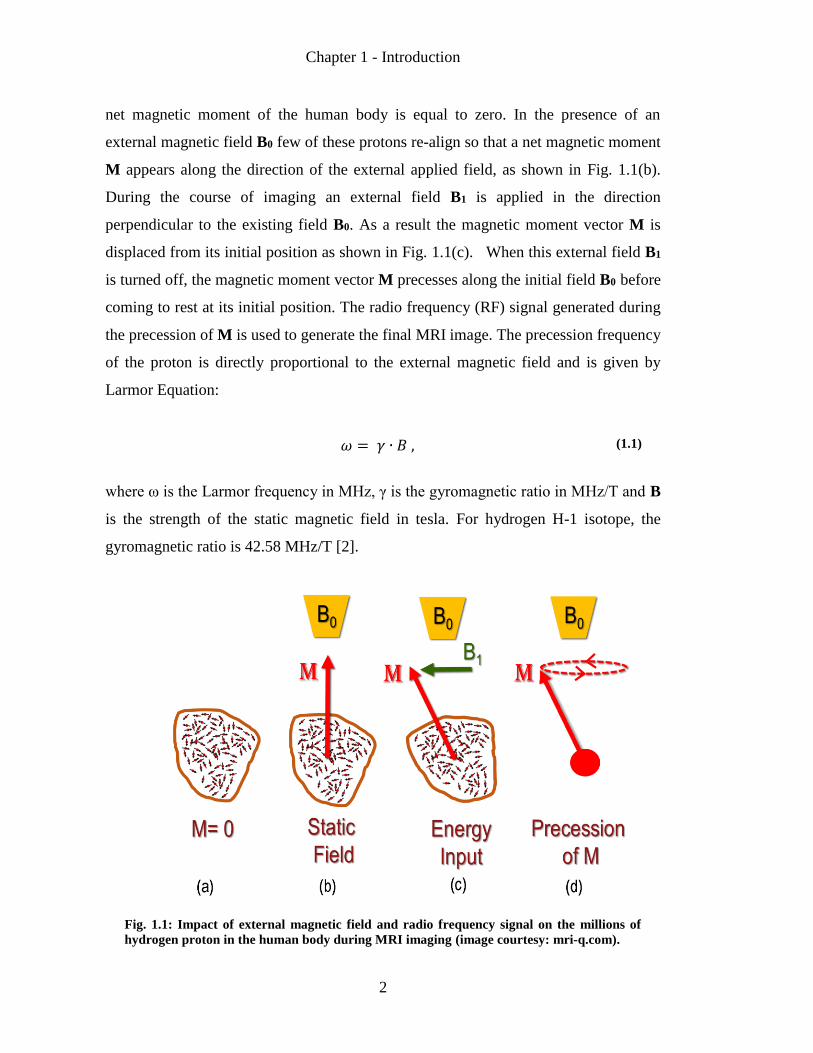
net magnetic moment of the human body is equal to zero. In the presence of an
external magnetic field B0 few of these protons re-align so that a net magnetic moment
M appears along the direction of the external applied field, as shown in Fig. 1.1(b).
During the course of imaging an external field B1 is applied in the direction
perpendicular to the existing field B0. As a result the magnetic moment vector M is
displaced from its initial position as shown in Fig. 1.1(c). When this external field B1
is turned off, the magnetic moment vector M precesses along the initial field B0 before
coming to rest at its initial position. The radio frequency (RF) signal generated during
the precession of M is used to generate the final MRI image. The precession frequency
of the proton is directly proportional to the external magnetic field and is given by
Larmor Equation:
𝜔 = 𝛾 ∙ 𝐵 , (1.1)
where ω is the Larmor frequency in MHz, γ is the gyromagnetic ratio in MHz/T and B
is the strength of the static magnetic field in tesla. For hydrogen H-1 isotope, the
gyromagnetic ratio is 42.58 MHz/T [2].
Fig. 1.1: Impact of external magnetic field and radio frequency signal on the millions of
hydrogen proton in the human body during MRI imaging (image courtesy: mri-q.com).
Chapter 1 - Introduction
3
1.1.2 System Components
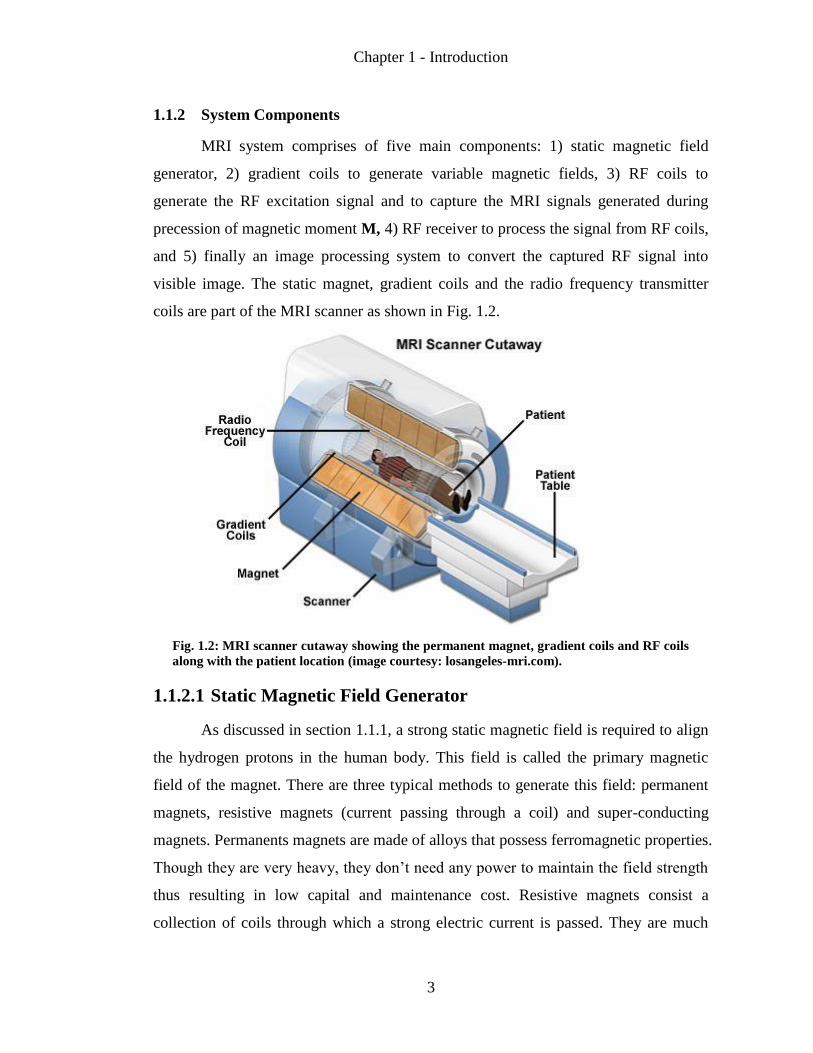
MRI system comprises of five main components: 1) static magnetic field
generator, 2) gradient coils to generate variable magnetic fields, 3) RF coils to
generate the RF excitation signal and to capture the MRI signals generated during
precession of magnetic moment M, 4) RF receiver to process the signal from RF coils,
and 5) finally an image processing system to convert the captured RF signal into
visible image. The static magnet, gradient coils and the radio frequency transmitter
coils are part of the MRI scanner as shown in Fig. 1.2.
Fig. 1.2: MRI scanner cutaway showing the permanent magnet, gradient coils and RF coils
along with the patient location (image courtesy: losangeles-mri.com).
1.1.2.1 Static Magnetic Field Generator
As discussed in section 1.1.1, a strong static magnetic field is required to align
the hydrogen protons in the human body. This field is called the primary magnetic
field of the magnet. There are three typical methods to generate this field: permanent
magnets, resistive magnets (current passing through a coil) and super-conducting
magnets. Permanents magnets are made of alloys that possess ferromagnetic properties.
Though they are very heavy, they don’t need any power to maintain the field strength
thus resulting in low capital and maintenance cost. Resistive magnets consist a
collection of coils through which a strong electric current is passed. They are much

Chapter 1 - Introduction
4
lighter than the permanent magnets but need current to maintain their field strength.
Like resistive magnets, super conducting magnets also have coils through which
current is passed to generate the magnetic fields. However, these coils are made up of
super conducting material that is cooled to absolute zero using liquid helium. This
results in a very strong, stable and homogenous magnetic field around these coils.
To achieve a high resolution image, the magnetic fields generated by these
magnets need to be very strong, homogenous in space and stable in time. Permanent
magnets and resistive magnets are generally restricted to field strengths below 0.4T
and hence cannot be used for high-resolution imaging. Super conducting magnets on
the other hand have produced fields as high 14.1T and hence are primarily used for the
majority of MRI imaging. A brief comparison of different magnet types is given in
Table 1-1 [1].
Table 1-1: Comparison of different magnet types
Magnet
Type
Advantages Disadvantages
Permanent No electricity, refrigeration
required,
Open architecture;
Limited fringe field;
Fields cannot be switched off;
Limited field strength;
Sensitive to temperature
changes;
Limited signal to noise ratio.
Resistive No refrigeration required;
Open architecture;
Fields can be switched off.
High electricity requirements;
Limited field strength;
Limited signal to noise ratio
Super-
Conducting
High signal to noise ratio;
Strong. homogenous and
stable magnetic fields;
High field strength.
High running cost, electricity
requirements;
Need special cooling;
Closed architecture, very noisy
and causes claustrophobia;
Switching off complicated and
Chapter 1 - Introduction
5
costly.
1.1.2.2 Gradient coils
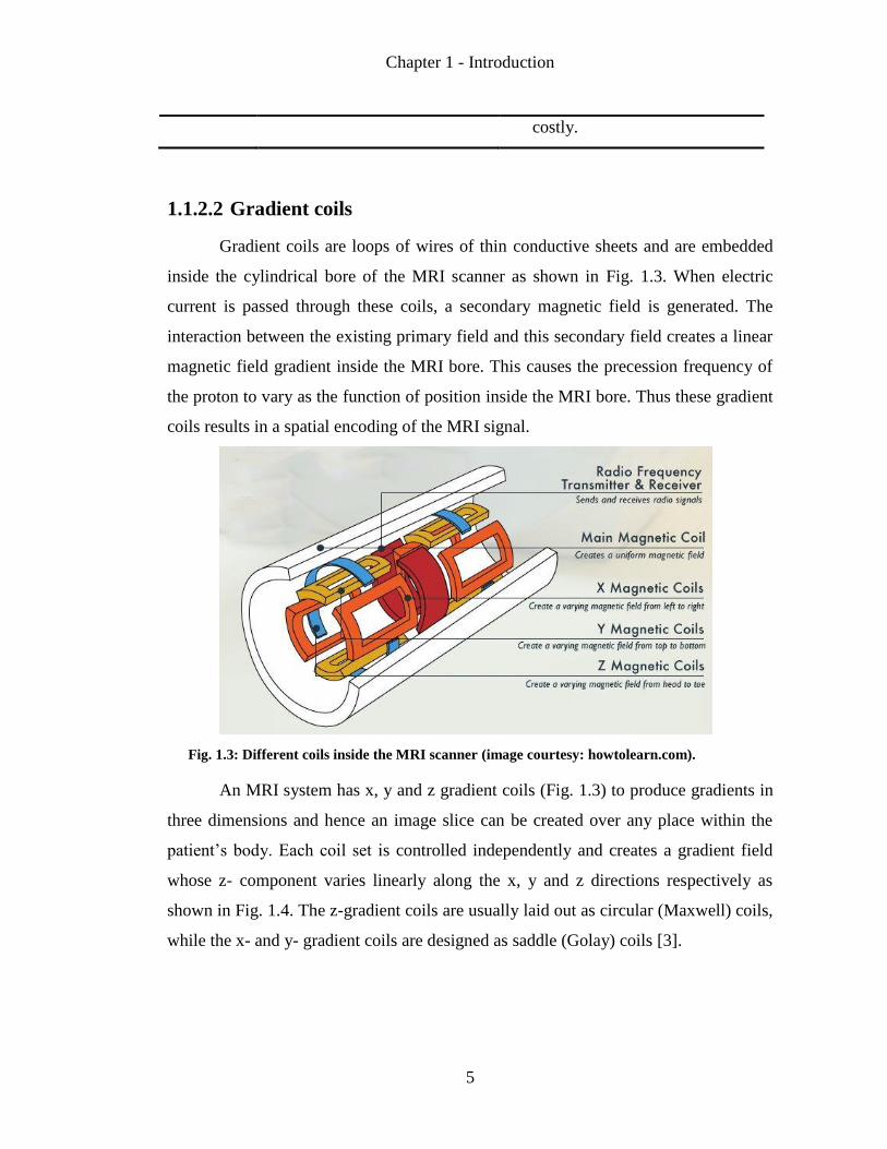
Gradient coils are loops of wires of thin conductive sheets and are embedded
inside the cylindrical bore of the MRI scanner as shown in Fig. 1.3. When electric
current is passed through these coils, a secondary magnetic field is generated. The
interaction between the existing primary field and this secondary field creates a linear
magnetic field gradient inside the MRI bore. This causes the precession frequency of
the proton to vary as the function of position inside the MRI bore. Thus these gradient
coils results in a spatial encoding of the MRI signal.
Fig. 1.3: Different coils inside the MRI scanner (image courtesy: howtolearn.com).
An MRI system has x, y and z gradient coils (Fig. 1.3) to produce gradients in
three dimensions and hence an image slice can be created over any place within the
patient’s body. Each coil set is controlled independently and creates a gradient field
whose z- component varies linearly along the x, y and z directions respectively as
shown in Fig. 1.4. The z-gradient coils are usually laid out as circular (Maxwell) coils,
while the x- and y- gradient coils are designed as saddle (Golay) coils [3].

Chapter 1 - Introduction
6
Fig. 1.4: Impact of different gradient coils on static magnetic field (image courtesy: mri-
q.com.
1.1.2.3 RF coils
RF coils can be divided into three main categories: transmit coils, receive coils
and transceiver coils, and they are chosen depending on the area of the body that needs
to be imaged. Transmit RF coils create the B1 field that rotates the net magnetization
vector during MRI imaging as shown in Fig. 1.1(c), whereas the receive coil is used to
capture the RF signal that is generated during precession and is hence used for MRI
image creation. The transceiver coil on the other hand can both generate the RF signal
and also capture the precession signal.
The RF coils are designed to resonate at the Larmor frequency, hence they
comprise of an inductive element (L) and a capacitive element (C). The inductive
element is provided by one or multiple windings of low-resistance metallic wire,
usually copper due to its non–magnetic properties. As the coil may need to be tuned
once it is placed on the patient’s body, the capacitive element comprises of a variable
capacitor. The resonant frequency of the coils is given by
𝑓𝑐𝑜𝑖𝑙 =
1
2𝜋√𝐿𝐶 .
(1.2)
Chapter 1 - Introduction
7
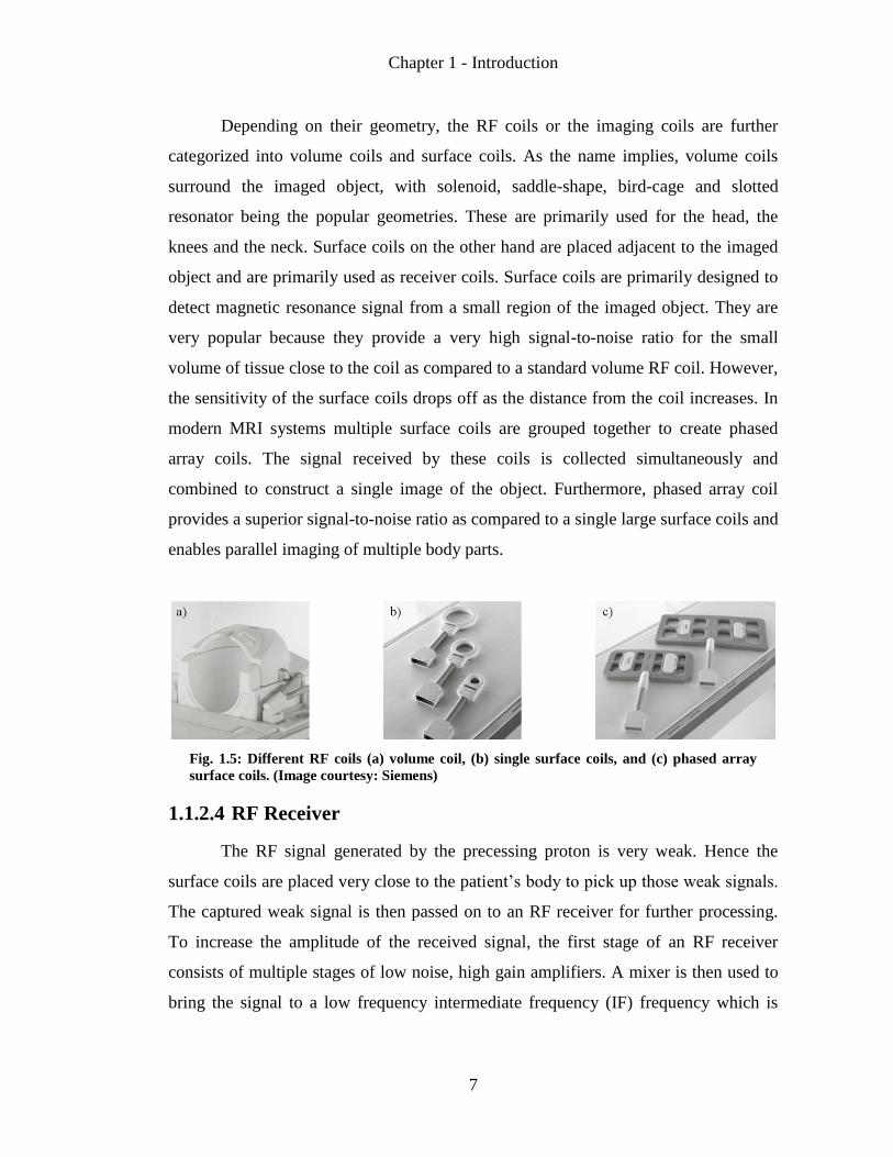
Depending on their geometry, the RF coils or the imaging coils are further
categorized into volume coils and surface coils. As the name implies, volume coils
surround the imaged object, with solenoid, saddle-shape, bird-cage and slotted
resonator being the popular geometries. These are primarily used for the head, the
knees and the neck. Surface coils on the other hand are placed adjacent to the imaged
object and are primarily used as receiver coils. Surface coils are primarily designed to
detect magnetic resonance signal from a small region of the imaged object. They are
very popular because they provide a very high signal-to-noise ratio for the small
volume of tissue close to the coil as compared to a standard volume RF coil. However,
the sensitivity of the surface coils drops off as the distance from the coil increases. In
modern MRI systems multiple surface coils are grouped together to create phased
array coils. The signal received by these coils is collected simultaneously and
combined to construct a single image of the object. Furthermore, phased array coil
provides a superior signal-to-noise ratio as compared to a single large surface coils and
enables parallel imaging of multiple body parts.
Fig. 1.5: Different RF coils (a) volume coil, (b) single surface coils, and (c) phased array
surface coils. (Image courtesy: Siemens)
1.1.2.4 RF Receiver
The RF signal generated by the precessing proton is very weak. Hence the
surface coils are placed very close to the patient’s body to pick up those weak signals.
The captured weak signal is then passed on to an RF receiver for further processing.
To increase the amplitude of the received signal, the first stage of an RF receiver
consists of multiple stages of low noise, high gain amplifiers. A mixer is then used to
bring the signal to a low frequency intermediate frequency (IF) frequency which is
Chapter 1 - Introduction
8
then converted to digital domain by a high resolution, low speed, 12-bit to 16-bit
analog-to-digital converter (ADC) [4]. This architecture uses low bandwidth ADC
with sampling rate less than 1MHz. However, signal can be directly sampled by using
a high-bandwidth, high-resolution, 12-bit to 16-bit ADC with sample rates up to
100MHz, thereby eliminating the analog mixer from the chain.
1.1.2.5 Image Processing
The raw data captured during the MRI imaging contains both the spatial
frequency and phase information of the precessing protons and is called as the k-space
data [3]. This k-space data is then processed using Fourier transform and converted to
a grey scale image of the object.
1.1.3 Drawbacks of Existing MRI Systems
With rapid advancements in the imaging technology and its wide ranging
benefits, MRI has widely emerged as one of the most accurate medical diagnostic
techniques available to physicians. Despite this, the cost of MRI is still prohibitively
high as compared to CT scan or normal X-ray. Apart from initial equipment cost, one
of the main contributors to the operating cost is the cost associated with the RF coils
used for imaging. As discussed in section 1.1.2.3, to get a high resolution image, the
surface receiver coils need to be placed very close to the imaged object. Furthermore,
phased-array coils are used to improve the resolution even further. This implies that
separate receiver coils are required to image different parts of the human body so that
the coils conforms to the human body as shown in Fig. 1.6. Thus, hospitals and
imaging centers need to purchase and maintain separate sets of coils not only for
different body parts but also for people with different height, weight, and body types.
Moreover, these coils are not cheap. The cost of each coil can vary from $12,000 to
$120,000.
Apart from the cost, these coils can be quite ill-fitted and can be intimidating,
especially for children. As a result hospitals regularly administer anesthesia to the
children before performing an MRI which adds to the costs associated with MRI. Thus

Chapter 1 - Introduction
9
in order to reduce the cost of MRI, there is an urgent need to redesign the MRI
receiver coils.
Fig. 1.6: Separate receiver coils for different body part. (Image courtesy: Siemens)
1.1.4 Redesign MRI Receiver Coil
1.1.4.1 Modular Receiver Coil
As discussed in section 1.1.3, in order to a get a high resolution image via an
MRI system, the hospitals need to buy and maintain a lot of different types of receiver
coils. Being expensive, this adds to the overall cost of the MRI. One possible solution
is to use a modular coil instead of a single big coil. For example, a set of four element
phased- array coil can form a single MRI receiver coil module. If one needs to image a
smaller area of human body, one of these module can be used as shown in Fig. 1.7. To
image a bigger part of the body, multiple of these coils can be joined together like
Lego® bricks as shown in Fig. 1.8, thereby eliminating the need to buy different coils
for different body parts. Furthermore, to ensure that the four element unit can be used
as a building block for all the patients, these coils can be made even smaller.

Chapter 1 - Introduction
10
Fig. 1.7: A single four element phased array coils used for imaging (coil image courtesy:
Siemens).
Fig. 1.8: Multiple four element phased array coils combined together to create a single
image (coil image courtesy: Siemens).
Chapter 1 - Introduction
11
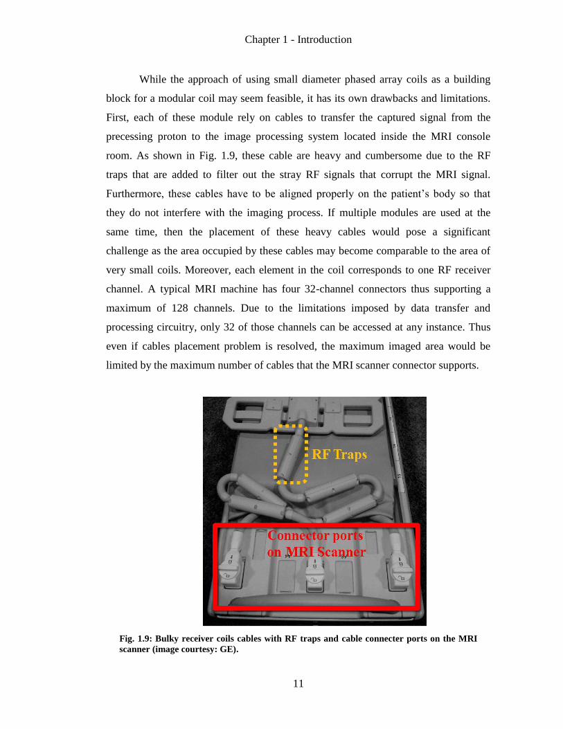
While the approach of using small diameter phased array coils as a building
block for a modular coil may seem feasible, it has its own drawbacks and limitations.
First, each of these module rely on cables to transfer the captured signal from the
precessing proton to the image processing system located inside the MRI console
room. As shown in Fig. 1.9, these cable are heavy and cumbersome due to the RF
traps that are added to filter out the stray RF signals that corrupt the MRI signal.
Furthermore, these cables have to be aligned properly on the patient’s body so that
they do not interfere with the imaging process. If multiple modules are used at the
same time, then the placement of these heavy cables would pose a significant
challenge as the area occupied by these cables may become comparable to the area of
very small coils. Moreover, each element in the coil corresponds to one RF receiver
channel. A typical MRI machine has four 32-channel connectors thus supporting a
maximum of 128 channels. Due to the limitations imposed by data transfer and
processing circuitry, only 32 of those channels can be accessed at any instance. Thus
even if cables placement problem is resolved, the maximum imaged area would be
limited by the maximum number of cables that the MRI scanner connector supports.
Fig. 1.9: Bulky receiver coils cables with RF traps and cable connecter ports on the MRI
scanner (image courtesy: GE).

Chapter 1 - Introduction
12
1.1.4.2 Proposed Modular Wireless Receiver Coil
The main challenge towards the adoption of modular receiver coils is the
presence of heavy cables and its associated limitations. The coil setup time can be a
significant fraction of the total exam time. Consequently, removing these cables from
the receiver coil will lead to a more cost effective and time efficient system. In the past,
a number of architectures have been proposed to enable wireless MRI [5][6][7][8][9] -
[10] for minimizing or removing the cables. All these efforts use microwave
frequencies up to 3GHz, and protocols such as 802.11b or MIMO that are intended for
long-range communication over distances of 10 m to 100 m. This results in a sub-
optimal solution for wireless MRI in terms of power consumption and size.
Here, we propose a custom millimeter (mm) wave transceiver architecture that
meets the requirements for wireless MRI at minimum power consumption and size. A
block diagram is shown in Fig. 1.10, and a possible architecture for the proposed
wireless receiver coils is shown in Fig. 1.11. An earlier version of this transceiver has
been used for short range, high data-rate, near field communication (NFC) system [11].
The mm-wave transmitter (TX) would be located on the receiver coil jacket while the
mm-wave receiver (RX) can be embedded inside the MRI system’s bore tube. Once
the data is received at the bore tube over the mm-wave wireless link, a fiber optic
transceiver converts electrical signal into the optical domain. A fiber optic cable
transfers this data from the MRI bore to the scanner console room. A second fiber
optic transceiver converts this signal back to electrical domain. The data is then
further processed to obtain the final image. The transceiver operates in mm-wave
frequencies with an RF carrier at 60 GHz using on-off key (OOK) modulation.
Fig. 1.10: Block diagram of the proposed wireless MRI system

Chapter 1 - Introduction
13
Fig. 1.11: Receiver coil with wireless transmitter.
1.2 Organization
In chapter 2, different architectures for the proposed wireless receiver coil are
presented along with a brief survey of competing wireless technologies. The
architecture and design details for the proposed wireless MRI system are then
discussed in chapter 3. Chapter 4 describes the test setup and the measurement results
for the proposed system and chapter 5 concludes the discussion along with the
direction for future research.

Chapter 2 - Wireless Receiver Coil
14

Chapter 2 - Wireless Receiver Coil
15
CHAPTER 2
Wireless Receiver Coil
2.1 Wireless Receiver Coil Architectures
The number of elements in a receiver coil can vary from 1 to 32, depending on
the area of the body to be imaged. Furthermore, to ensure conformity to the body part
to be imaged, coils with same number of elements may have different shapes and sizes.
For improved SNR, parallel imaging performance, and field of view (FOV), the
maximum number of elements will go to 128 elements in the near future. Thus, the
first step to eliminate separate receiver coils for different scenarios and replace it with
a universal receiver coil design is to pick up an architecture for modular receiver coil.
2.1.1 Single-Element Module
A single element module would offer maximum flexibility in terms of its reuse,
as multiple single element modules can be placed simultaneously to image different
parts of human body. Each receiver coil would have a separate data processing unit
and a wireless transceiver which may result in a high system power consumption. As
the coils may have to be placed in closed proximity during imaging, the signal from
adjacent wireless channels may interfere with each other. This will impose limitations
on the minimum distance between the coils. Furthermore, the choice of wireless
technology may also restrict the maximum number of coils that can be used
simultaneously.
2.1.2 Multi Element Module
A multi-element module can have anywhere between 2 to 32 elements. In a
multi-element module, data from different elements can be collated and processed
using a single data processing unit. It can then be transmitted using a single wireless
transmitter (TX). To ensure data integrity, the data and clock signal between different
elements would have to be synchronized. This would require a careful design of
Chapter 2 - Wireless Receiver Coil
16
routing between individual coils and shared data processing unit. The MRI signal may
couple to these connections thereby corrupting the data being processed. Furthermore,
the routing complexity would increase with the number of elements in the module.
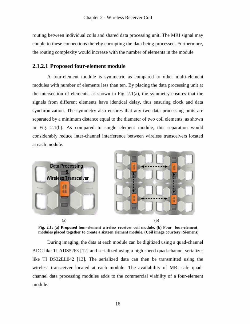
2.1.2.1 Proposed four-element module
A four-element module is symmetric as compared to other multi-element
modules with number of elements less than ten. By placing the data processing unit at
the intersection of elements, as shown in Fig. 2.1(a), the symmetry ensures that the
signals from different elements have identical delay, thus ensuring clock and data
synchronization. The symmetry also ensures that any two data processing units are
separated by a minimum distance equal to the diameter of two coil elements, as shown
in Fig. 2.1(b). As compared to single element module, this separation would
considerably reduce inter-channel interference between wireless transceivers located
at each module.
(a) (b)
Fig. 2.1: (a) Proposed four-element wireless receiver coil module, (b) Four four-element
modules placed together to create a sixteen element module. (Coil image courtesy: Siemens)
During imaging, the data at each module can be digitized using a quad-channel
ADC like TI ADS5263 [12] and serialized using a high speed quad-channel serializer
like TI DS32EL042 [13]. The serialized data can then be transmitted using the
wireless transceiver located at each module. The availability of MRI safe quad-
channel data processing modules adds to the commercial viability of a four-element
module.

Chapter 2 - Wireless Receiver Coil
17
Even though a four-element coil has been proposed as a preferred architecture,
a single-element coil architecture cannot be discarded. A single-element coil might be
useful for scenarios where a very small area needs to be imaged that might be too big
for a multi-element coil. Furthermore, to generate high resolution images, future MRI
systems may require access to raw data generated by the sampling ADCs which is of
the order of gigabits per second. In such a scenario, a single coil architecture might be
the only feasible solution due to the data rate limitations imposed by the commercially
available wireless technologies.
2.2 Wireless Technologies
During imaging, the receiver coil captures the signal generated by the
precessing proton as discussed in Chapter 1. As this signal is very weak, it is amplified
using low noise, high-gain amplifiers and sent to the MRI console room via cables for
further processing. In case of wireless receiver coils, after initial amplification, the
receiver coil data can be digitized using MRI compatible analog-to-digital convertor
(ADC) like Texas Instruments (TI) ADS5263 [12]. ADS5263 is a 4 channel, 16-bit,
100 MS/s ADC with in-built decimation. This results in a raw data of 1.6 Gb/s for
each element of the receiver coil. As the MRI data is very narrow band, it can be
decimated to get an effective data rate of 20 Mb/s for each element. Thus depending
on receiver coil architecture and digital data processing, the data rates for wireless
receiver coil module may vary from megabits per second to gigabits per second.
Therefore, the wireless TX placed on the receiver coil should support high data rates.
For wireless receiver coils, the TX would be powered by a non-magnetic battery or by
energy harvesting circuits. This makes TX power consumption an important criteria
for system design. Moreover, in a modular approach to receiver coil design, several of
these TXs might be placed in close proximity, resulting in high inter channel
interference. In such a scenario, these TXs need to be placed and orientated to
minimize this interference. Finally, if the wireless receiver is embedded inside the
MRI system bore tube, the distance between the TX and the receiver would be less
than one meter. Thus wireless MRI requires a low power, high-data rate, and scalable
Chapter 2 - Wireless Receiver Coil
18
solution that can work up to one meter and some of the competing technologies are
discussed in the next section.
2.2.1 Wi-Fi 802.11ac
802.11ac is the latest standard from IEEE and is the first one to support Gb/s
data rates in the traditional 5 GHz band. 802.11ac supports multiple channel
bandwidths (20 MHz, 40 MHz, 80 MHz, and 160 MHz), multiple modulation schemes
(binary phase shift keying (BPSK), quadrature phase shift keying (QPSK), 16-
quadrature amplitude modulation (QAM), 64-QAM, and 256-QAM) and up to eight
spatial streams for multiple input, multiple output (MIMO) [14]. The system provides
twenty five 20MHz channels which can be joined to form twelve 40MHz channels or
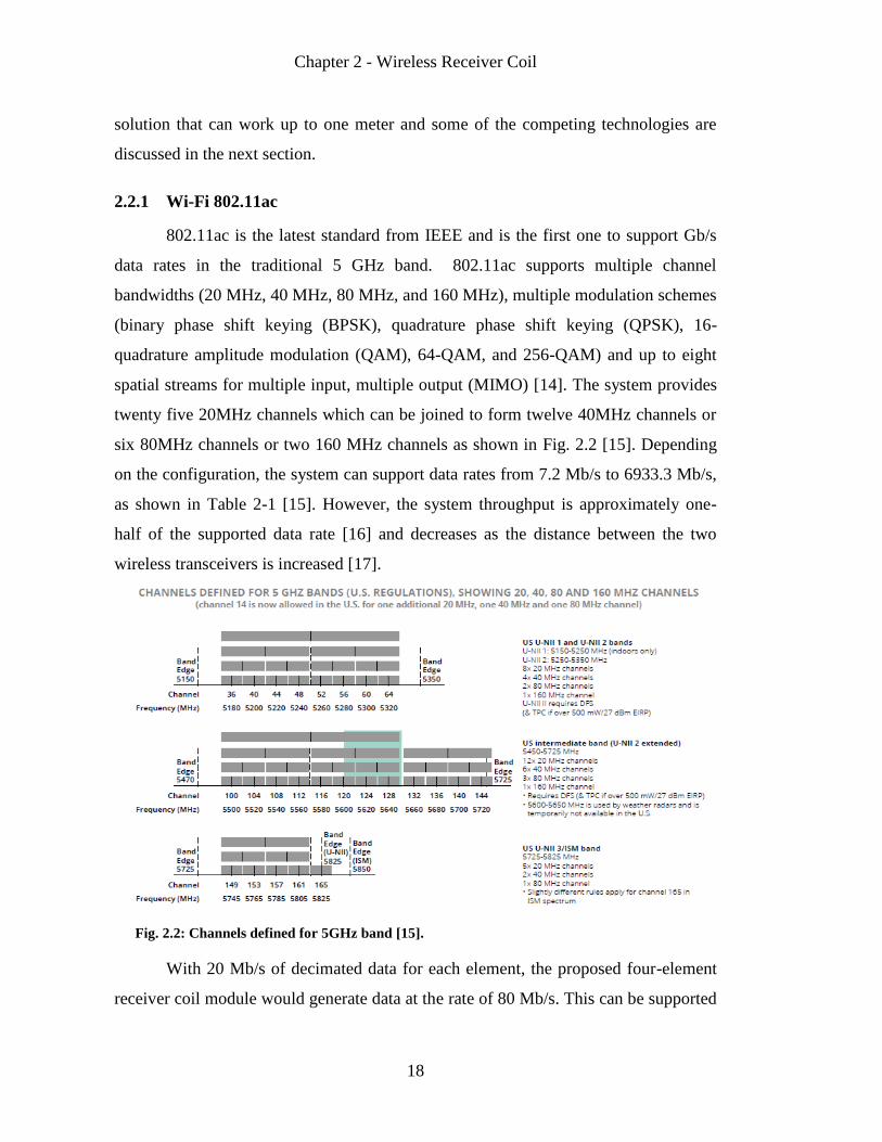
six 80MHz channels or two 160 MHz channels as shown in Fig. 2.2 [15]. Depending
on the configuration, the system can support data rates from 7.2 Mb/s to 6933.3 Mb/s,
as shown in Table 2-1 [15]. However, the system throughput is approximately one-
half of the supported data rate [16] and decreases as the distance between the two
wireless transceivers is increased [17].
Fig. 2.2: Channels defined for 5GHz band [15].
With 20 Mb/s of decimated data for each element, the proposed four-element
receiver coil module would generate data at the rate of 80 Mb/s. This can be supported

Chapter 2 - Wireless Receiver Coil
19
by either using two parallel streams of 20 MHz or a single 40 MHz stream. For a
MIMO system, each stream requires its own antenna with a minimum physical
separation of lambda-by-2 between them and a suggested separation of four lambda
[18] for optimal performance. This would lead to an antenna separation of ~1.1ʺ to ~9ʺ
for the 5 GHz band. The size of a single element in the receiver coil can vary from
2.5ʺ to 8ʺ. Therefore, having multiple antennas on each module would increase the
design complexity in terms of routing to different antennas, as well as the required
abutting of multiple modules to image a wider section of human body. Hence a single
antenna, with 256-QAM single stream 40 MHz channel, supporting 200 Mb/s data rate
would be a preferred solution.
Table 2-1: 802.11ac data rates for different modulations and spatial streams [15].
With twelve 40 MHz channels and a dedicated TX and receiver (RX) for every
four-element module, the 802.11ac can support a maximum of 48 elements
simultaneously. This is assuming that each TX-RX pair occupies a separate channel.
More modules can be supported by using time-division multiplexing. Here data from
different TXs would go to a single RX. However, this would require the MRI data to
be buffered at each TX while it waits for its turn to transmit. With data rates of 80
Mb/s for each module, this could result in a significant power and memory overhead.
Chapter 2 - Wireless Receiver Coil
20
On the other hand, for a single-element module, even 160MHz bandwidth channel
doesn’t support 1.6 Gb/s of raw data generated at the coil.
In terms of power consumption, with a complex modulation schemes of 256-
QAM and orthogonal frequency division multiplexing (OFDM) signaling schemes, the
average power consumption of an 802.11ac system at maximum data rates is ~10
nJ/bit. This results in a power consumption of 2W for each module [19] and does not
scale linearly with data rate.
2.2.2 802.11ad
The IEEE 802.11ad standard uses the 8 GHz unlicensed band at 60-GHz and is
aimed at providing data rates up to 7 Gb/s. High path loss at 60-GHz and the
availability of a wider bandwidth makes 802.11ad an ideal candidate for short range,
high data rate communication system with distances up to 10 m. The international
telecommunication union (ITU) recommends the use of four channels, each 2.16 GHz
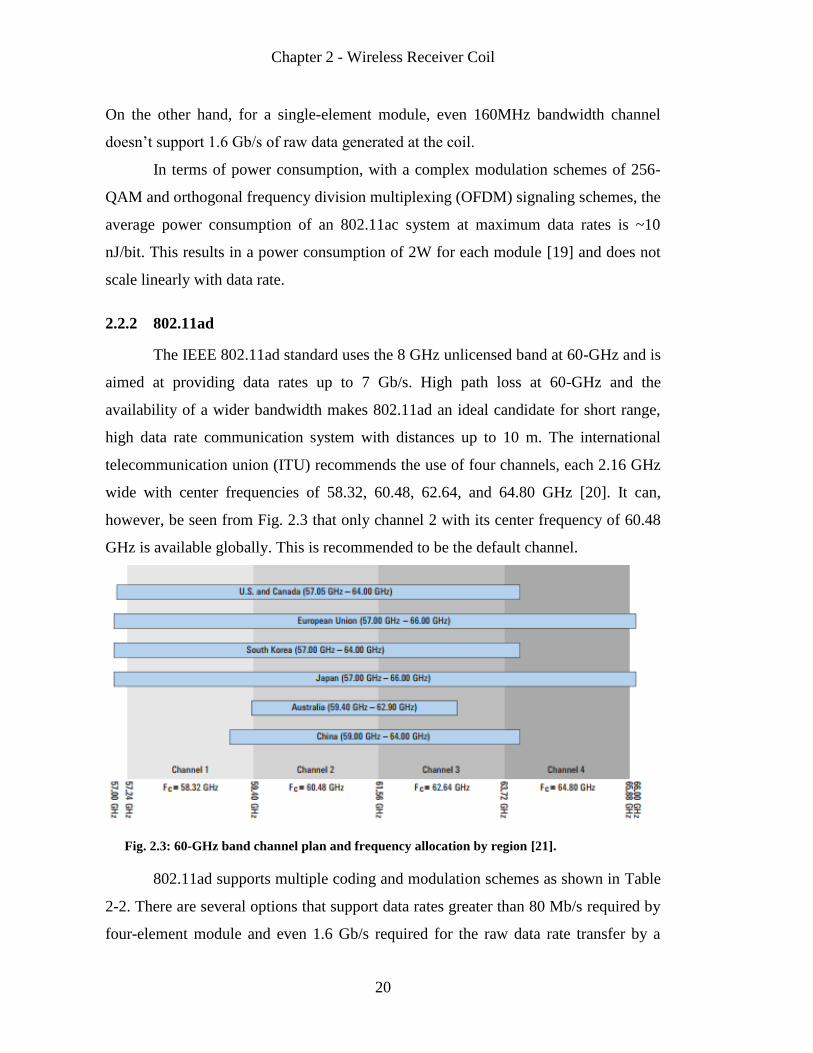
wide with center frequencies of 58.32, 60.48, 62.64, and 64.80 GHz [20]. It can,
however, be seen from Fig. 2.3 that only channel 2 with its center frequency of 60.48
GHz is available globally. This is recommended to be the default channel.
Fig. 2.3: 60-GHz band channel plan and frequency allocation by region [21].
802.11ad supports multiple coding and modulation schemes as shown in Table
2-2. There are several options that support data rates greater than 80 Mb/s required by
four-element module and even 1.6 Gb/s required for the raw data rate transfer by a

Chapter 2 - Wireless Receiver Coil
21
single element module. There are multiple companies [22][23] - [24] providing low
power 802.11ad chips with energy efficiency of ~50pJ/bit at the highest data rate,
which is orders of magnitude better than that offered by 802.11ac systems. With
support for required data rate and superior energy efficiency, 802.11ad seems like a
viable solution for wireless receiver coils. However, all the commercial solutions are
designed to support distances up to 10 meter and operate at the maximum data rate of
around 4 Gb/s. As they need to adhere to linear modulation schemes like OFDM, the
system power remains constant irrespective of the data rate. Thus even while
transmitting data at 80 Mb/s, the 802.11 ad system would consume ~200mW of power.
There are few low power solutions offered by SiBEAM™ [22] as a replacement for a
physical universal serial bus (USB) connector. However, this low power solution
works for distances less than 1 cm and hence can’t be used for wireless receiver coils.
Wireless USB may become a viable alternative if its range is extended to 1 m in near
future. Availability of only one single channel may significantly increase the
interference between multiple TXs as they are placed in closed proximity inside the
MRI system bore tube while imaging. This can be mitigated by using beam forming at
each TX and time division multiplexing between multiple TXs.
Table 2-2: 802.11AD MODULATION AND CODING SUMMARY [20]

Chapter 2 - Wireless Receiver Coil
22
2.2.3 Custom Millimeter (mm)-Wave Solution
Based on the discussion in previous sections, 60-GHz seems to be a possible
solution for modular wireless MRI receiver coils. However, the limitations imposed by
existing 802.11ad standard warrants the need of a custom solution. The processing
overheads and limitations imposed by complex modulation schemes such as OFDM
results in a high power consumption in existing 60-GHz solutions. This can be
resolved by using simpler modulation schemes such as on-off keying (OOK). In OOK,
the TX consumes power while it is transmitting ‘1’ and is OFF when it is transmitting
‘0’. This can reduce the system power consumption by a factor of two as compared to
conventional TXs that are ON all the time. The use of non-coherent modulation like
OOK simplifies the system architecture as the TX and the RX don’t need to be phase
synchronized. As the absolute phase of the system is not a concern, it relaxes the
linearity constraints for the power amplifier (PA) design, thus allowing the use of a
more efficient non-linear PA. This reduces system power consumption so that they can
be powered using tiny non-magnetic batteries. With OOK modulation at its core, a
custom mm-wave transceiver was designed that meets the requirements of wireless
MRI system. The system uses 60-GHz as the RF carrier frequency. The TX power of
the proposed system scales from 1.3 mW to 14.0 mW as the data rate is varied from
200 Mb/s to 2500 Mb/s, while the RX consumes a fixed DC power of 76 mW. The 60-
GHz radio occupies an area of 1.62 mm2 in TSMC 40 nm CMOS GP process and
would be discussed next.

Chapter 3 - Millimeter-Wave Wireless Transceiver
23
CHAPTER 3
Millimeter-Wave Wireless Transceiver
3.1 Proposed mm-Wave Transceiver v/s Prior Art
Numerous transceiver architectures have been proposed since the inception of
60-GHz as a viable band for civilian application. All these architectures can be
broadly classified into two categories. The first category focuses on providing a
reliable wireless link at long range ( 1 - 10 m), and maximizes data rate by enhancing
the spectral efficiency at the expense of high power consumption and costly antenna-
chip packaging technology [25] - [26][27][28][29]. Examples are wireless docking [30]
and wireless HD [31]. The long range requirement necessitates the use of high gain
off-chip antennas in two-dimensional arrays for beam-forming [32], [33]. In order to
achieve high spectral efficiency, more symbols need to be packed into a limited band-
width (BW), hence forcing the system to apply more complex modulations such as 16
QAM and 64 QAM. These modulation schemes in turn increase the system linearity
and noise requirements. The design of linear radio frequency (RF) front-ends, low
noise RF and base-band (BB) blocks, and low phase noise local oscillator (LO) further
increases the power consumption and complexity of these radios [25]- [28]. Since
beam-forming is an integral part of this category of transceivers, additional challenges
arise in the implementation of phase shifters in either RF, LO, BB, or any other
combination [32] - [33][34][35][36][37][38][39]. These complexities increase the cost,
size, and power consumption of a product, hence limiting the use of 60 GHz radios in
mass markets.
The second category of 60 GHz radios, to which this work belongs, targets at
applications that require high data rate, low power, and short range (< 1 m) wireless
link. In general, these systems use relatively simpler modulation schemes such as
QPSK (coherent) and OOK (non-coherent). When coherent modulations are used, the
relative phase between the transmitter and receiver needs to be maintained. The
Chapter 3 - Millimeter-Wave Wireless Transceiver
24
requirement of phase alignment necessitates the use of a phase lock loop (PLL) in both
the transmitter and receiver. For 60-GHz systems, the PLL and the LO in-phase (I)
and quadrature (Q) generation consume substantial power. In [40], a 4 × 4 QPSK
transceiver with on-chip antennas is demonstrated with high data rate and energy
efficiency. However, its transmitter consists of four free running VCOs and it assumes
that the receiver LO knows the frequency of these VCOs. This architecture with its
assumption will severely complicate demodulation in a practical system. On the other
hand, in systems using non-coherent modulation, the transmitter carrier frequency
does not need to be synchronized with the receiver LO. In fact, OOK with the
envelope detection in the receiver can be implemented without the LO requiring a PLL
in either the receiver or transmitter. Since LO generation consumes significant portion
of the total power, its elimination substantially reduces the power consumption [41],
[42]. A 1 × 1 OOK transceiver with on-chip antennas is reported in [43] where it uses
return-to-zero (RZ) signaling with pulse-width control (PWC) to reduce the power
consumption.
To meet the requirements of the wireless MRI systems, a very low cost, low
power and fully integrated 2 × 2 60-GHz transceiver with on-chip antennas has been
designed. The transceiver has a small silicon area of 1.62 mm2, including energy
harvesting circuits, and is suitable for near-range communication. The 2 × 2 system
improves the link budget and consequently the communication distance. Utilizing the
large bandwidth available at 60-GHz, this impulse-radio ultra-wideband transceiver
uses RZ-OOK modulation in conjunction with PWC to significantly reduce its power
consumption. A low-loss transmit-receive (TR) switch allows for the sharing of two
dipole antennas between the transmitter and receiver, allowing for a very small silicon
area. Furthermore, a low-power transmitter ensures that the energy harvested at the
unlicensed ISM band of 2.45 GHz is sufficient to power up the transceiver in the
transmit mode.
Harvesting energy at 2.45 GHz for a radio link at 60-GHz has important
advantages. Because of the large separation between the 60-GHz and 2.45 GHz
frequencies, a potentially high power harvesting signal would not desensitize the 60-

Chapter 3 - Millimeter-Wave Wireless Transceiver
25
GHz receiver. This is because the 60-GHz antenna and the receiver would sufficiently
attenuate an out of band jammer such as the one at 2.45 GHz. If the harvest and the
radio link frequencies were close to each other, extra filtering would have been
necessary to eliminate a desensitization scenario. Such extra filtering would add cost
and further insertion loss to the system.
Fig. 3.1: (a) Linear relationship between the data rate and transmit power consumption. (b)
Application in point of sale advertisement. (c) Application in medium to high data rate:
neural data transmission of small beings.
Finally, apart from wireless MRI, the designed transceiver could be used for
different applications in consumer electronics and the future internet of things (IoT),
depending on the power and data rate requirements. As shown in Fig. 3.1(a), data rate
linearly scales with the transmitter power consumption, hence providing an agile
platform to support various applications. This radio could be used as an alternative to
the near field communication (NFC), enabling substantially higher data rate and
energy harvesting capability. Fig. 3.1(b) shows another application of this radio as an
enabler of point of sale advertisement, which could become a major trend in the
emerging IoT markets. As illustrated in Fig. 3.1(c), the small size of the radio can
enable neural data transmission of small beings and insects where wireless
communication at longer wavelengths could present a mechanical challenge to the
biological experimentation due to the large size of the antenna.
3.2 Transceiver Architecture
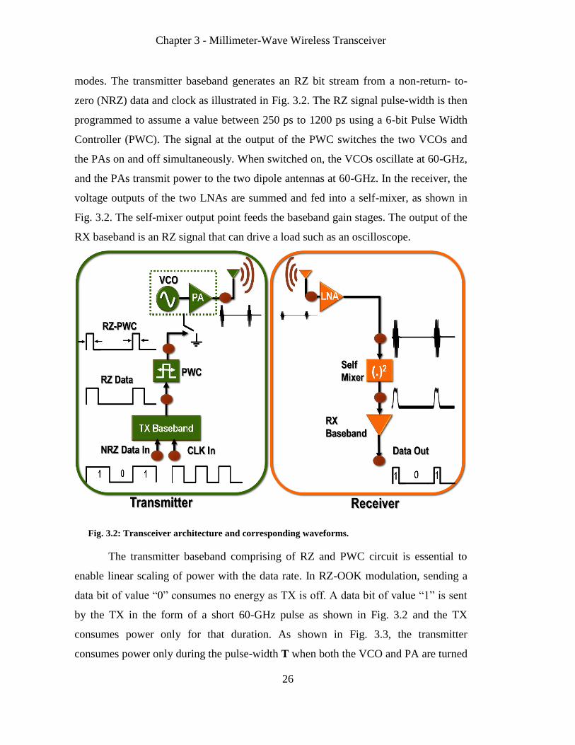
The 60-GHz transceiver architecture along with the TX and RX timing
diagram is depicted in Fig. 3.2 . In a time-division duplexing (TDD) communication, a
TR switch enables the two dipole antennas to be shared between the RX and TX
Chapter 3 - Millimeter-Wave Wireless Transceiver
26
modes. The transmitter baseband generates an RZ bit stream from a non-return- to-
zero (NRZ) data and clock as illustrated in Fig. 3.2. The RZ signal pulse-width is then
programmed to assume a value between 250 ps to 1200 ps using a 6-bit Pulse Width
Controller (PWC). The signal at the output of the PWC switches the two VCOs and
the PAs on and off simultaneously. When switched on, the VCOs oscillate at 60-GHz,
and the PAs transmit power to the two dipole antennas at 60-GHz. In the receiver, the
voltage outputs of the two LNAs are summed and fed into a self-mixer, as shown in
Fig. 3.2. The self-mixer output point feeds the baseband gain stages. The output of the
RX baseband is an RZ signal that can drive a load such as an oscilloscope.
Fig. 3.2: Transceiver architecture and corresponding waveforms.
The transmitter baseband comprising of RZ and PWC circuit is essential to
enable linear scaling of power with the data rate. In RZ-OOK modulation, sending a
data bit of value “0” consumes no energy as TX is off. A data bit of value “1” is sent
by the TX in the form of a short 60-GHz pulse as shown in Fig. 3.2 and the TX
consumes power only for that duration. As shown in Fig. 3.3, the transmitter
consumes power only during the pulse-width T when both the VCO and PA are turned
Chapter 3 - Millimeter-Wave Wireless Transceiver
27
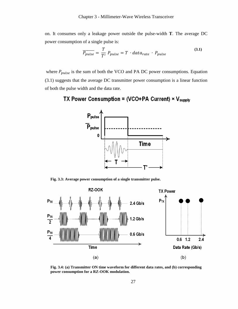
on. It consumes only a leakage power outside the pulse-width T. The average DC
power consumption of a single pulse is:
𝑃𝑝𝑢𝑙𝑠𝑒 =
𝑇
𝑇′ 𝑃𝑝𝑢𝑙𝑠𝑒 = 𝑇 ∙ 𝑑𝑎𝑡𝑎𝑟𝑎𝑡𝑒 ∙ 𝑃𝑝𝑢𝑙𝑠𝑒
(3.1)
where 𝑃𝑝𝑢𝑙𝑠𝑒 is the sum of both the VCO and PA DC power consumptions. Equation
(3.1) suggests that the average DC transmitter power consumption is a linear function
of both the pulse width and the data rate.
Fig. 3.3: Average power consumption of a single transmitter pulse.
Fig. 3.4: (a) Transmitter ON time waveform for different data rates, and (b) corresponding
power consumption for a RZ-OOK modulation.

Chapter 3 - Millimeter-Wave Wireless Transceiver
28
In case of RZ-OOK modulation, the transmit pulse width increases
proportionally with the data rate as demonstrated in Fig. 3.4(a), hence transmitter
power consumption is constant irrespective of the data rate as shown in Fig. 3.4(b).
However, for RZ-PWC-OOK, the transmit pulse width remains constant for different
data rates as shown in Fig. 3.5(a). As a result, the transmitter power consumption
scales linearly with data rate as shown in Fig. 3.5(b).
Fig. 3.5: (a) Transmitter ON time waveform for different data rates, and (b) corresponding
power consumption for a RZ-PWC-OOK modulation.
3.3 Transmitter Design
In the proposed transceiver, the transmitter has two separate transmitting
elements that are fully symmetric. As shown in Fig. 3.6, each transmit element
consists of a VCO and a PA. The VCO drives the PA input and the PA drives a
differential dipole antenna.
Fig. 3.6: 2×2 Transceiver RF blocks.
Chapter 3 - Millimeter-Wave Wireless Transceiver
29
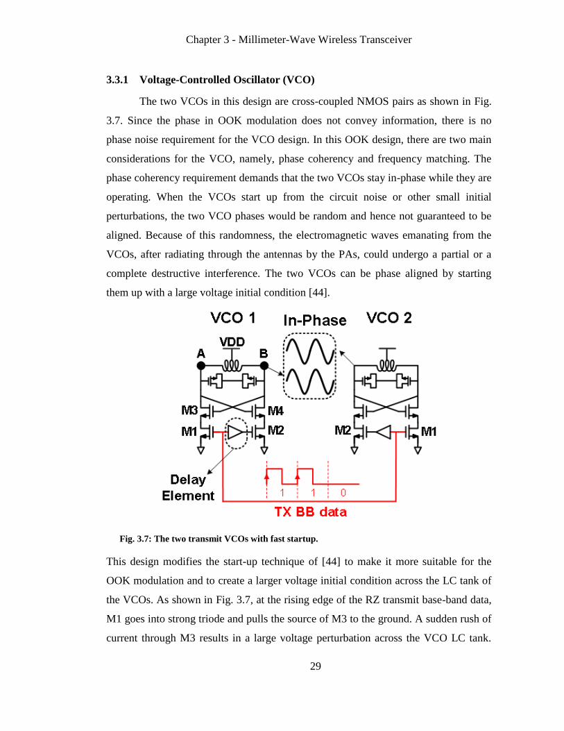
3.3.1 Voltage-Controlled Oscillator (VCO)
The two VCOs in this design are cross-coupled NMOS pairs as shown in Fig.
3.7. Since the phase in OOK modulation does not convey information, there is no
phase noise requirement for the VCO design. In this OOK design, there are two main
considerations for the VCO, namely, phase coherency and frequency matching. The
phase coherency requirement demands that the two VCOs stay in-phase while they are
operating. When the VCOs start up from the circuit noise or other small initial
perturbations, the two VCO phases would be random and hence not guaranteed to be
aligned. Because of this randomness, the electromagnetic waves emanating from the
VCOs, after radiating through the antennas by the PAs, could undergo a partial or a
complete destructive interference. The two VCOs can be phase aligned by starting
them up with a large voltage initial condition [44].
Fig. 3.7: The two transmit VCOs with fast startup.
This design modifies the start-up technique of [44] to make it more suitable for the
OOK modulation and to create a larger voltage initial condition across the LC tank of
the VCOs. As shown in Fig. 3.7, at the rising edge of the RZ transmit base-band data,
M1 goes into strong triode and pulls the source of M3 to the ground. A sudden rush of
current through M3 results in a large voltage perturbation across the VCO LC tank.

Chapter 3 - Millimeter-Wave Wireless Transceiver
30
The same voltage rising edge arrives at the gate of M2 after a time delay, which is
provided by the two cascaded inverters. Therefore, M2 turns on and enters into a
strong triode. To ensure proper differential operation, M2 should turn on after a delay
of half a period. Thus the two cascaded invertors provide a delay of 1/2𝑓0 = 8 ps for
the 60 GHz VCO. At this point the differential voltage across the VCO LC tank is
large, for example, 200 mV. This ensures both VCOs start at the same phase and
quickly reach a maximum swing.
The other requirement is the frequency matching between the VCOs. Since the VCOs
are open loop, their exact frequencies cannot be determined. There is a coarse 2 bit
digital-to-analog (DAC) that is connected to the control voltage of an NMOS varactor
pair, but it is only used to center the VCO frequency at a desirable channel within the
57–64 GHz range.

Chapter 3 - Millimeter-Wave Wireless Transceiver
31
Fig. 3.8: Beat frequency generation due to transmit VCOs' mismatch.
Fig. 3.8 illustrates the case in which the two VCOs have a frequency difference
of 2∆𝑓 . The spatial power of the EM waves emanating from the two VCOs will
combine to form a beat with a frequency of ∆𝑓. Here the coherence time, 𝑡𝑐𝑜ℎ𝑜𝑟𝑒𝑛𝑐𝑒,
of the two VCOs is defined as the time in which the spatially combined signal loses
half of its power i.e.,
cos(2𝜋∆𝑓𝑡𝑐𝑜ℎ𝑜𝑟𝑒𝑛𝑐𝑒) =
1
√2
⇒ 𝑡𝑐𝑜ℎ𝑜𝑟𝑒𝑛𝑐𝑒 =
1
8∆𝑓.
(3.2)
The frequency of an LC oscillator is given by
𝑓 =
1
2𝜋√𝐿𝐶 , (3.3)
Chapter 3 - Millimeter-Wave Wireless Transceiver
32
where 𝐿 and 𝐶 are the effective inductance and capacitance of the oscillator
respectively. Considering the variation in the effective inductance, ∆𝐿, is negligible
compared to the variation in the effective capacitance, ∆𝐶, the frequency variation can
be simplified as:
∆𝑓 =
1
2 ∙
Δ𝐶
C ∙ 𝑓 ,
(3.4)
By substituting (3.4) in (3.2), the coherence time of the VCOs is found to be:
𝑡𝑐𝑜ℎ𝑜𝑟𝑒𝑛𝑐𝑒 =
1
4𝑓 (
Δ𝐶
C)
−1
. (3.5)
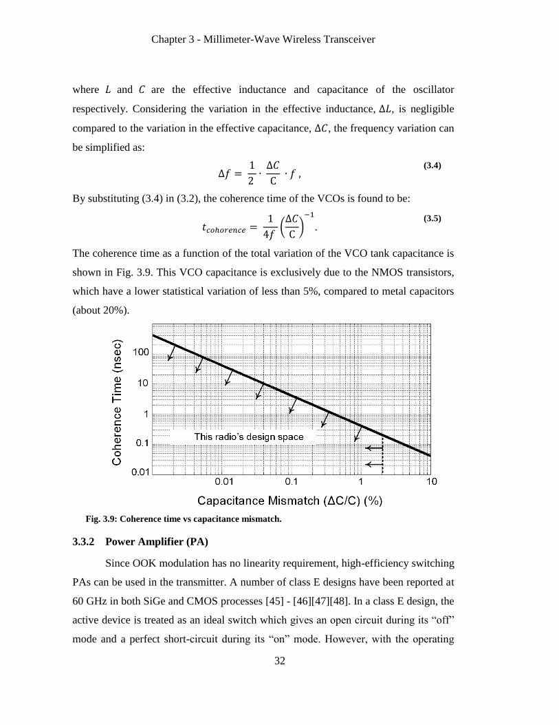
The coherence time as a function of the total variation of the VCO tank capacitance is
shown in Fig. 3.9. This VCO capacitance is exclusively due to the NMOS transistors,
which have a lower statistical variation of less than 5%, compared to metal capacitors
(about 20%).
Fig. 3.9: Coherence time vs capacitance mismatch.
3.3.2 Power Amplifier (PA)
Since OOK modulation has no linearity requirement, high-efficiency switching
PAs can be used in the transmitter. A number of class E designs have been reported at
60 GHz in both SiGe and CMOS processes [45] - [46][47][48]. In a class E design, the
active device is treated as an ideal switch which gives an open circuit during its “off”
mode and a perfect short-circuit during its “on” mode. However, with the operating

Chapter 3 - Millimeter-Wave Wireless Transceiver
33
frequency being a significant portion of the device transit frequency (fT), this ideal
switching is not possible thus leading to a sub-optimal class E operation [46]. On the
other hand, a class F-1 PA relies on harmonic tuned loads to shape the output voltage
and current waveforms.
Fig. 3.10: (a) Standard class F-1 PA. (b) Current and voltage waveforms for a class F-1 PA
with only one tank at third harmonic (solid) and ideal (dotted).
For example, Fig. 3.10(a) shows an ideal F-1 PA implementation. The high Q
resonators provide a short for third, fifth (odd) voltage harmonics while an open for all
even harmonics. This results in non-overlapping transistor voltage and current
waveforms as shown in Fig. 3.10(b). In a practical implementation, these high Q
resonators result in a significant area penalty and also introduce extra loss in the
output matching network.
The implemented PA is a combination of class E and class F-1 PA and is shown
in Fig. 3.11. Similar to class E PA, the drain cap Cdd is resonated out with drain
inductors L1A, 1B at the fundamental frequency of 60 GHz. At the same time, the drain
matching network consisting of capacitors Cdd, L1A, 1B, Cs and the dipole antenna is
designed as a harmonic tuned load akin to class F-1 PA. As a result its operation
resembles a class E/F2, odd PA [45]. This can be seen by comparing the simulated drain
voltage and current of the PA to the ideal class E/F2, odd PA as shown in Fig. 3.12.

Chapter 3 - Millimeter-Wave Wireless Transceiver
34
Fig. 3.11: The implemented class E/F2, odd PA.
The gate of transistors M1A, 1B is biased at a nominal voltage of 700 mV by a 3
bit resistor DAC, while the drain is connected to a supply voltage of 1 V. A tail
transistor, Mtail, enables quick turn on/off of the PA during OOK operation. When
turned on, the drain of Mtail is pulled to a lower potential (about 100 mV). Thus the
impact of Mtail on the output swing is minimized. With an average dc power
consumption of 13.5 mW, the PA delivers 4 mW of power at 60 GHz to a load, thus
achieving a drain efficiency of 29.6%.
Fig. 3.12: Drain Voltage (solid) and current (dotted) waveforms for (a) ideal class E/F2, odd
PA, and (b) implemented class E/F2, odd PA.
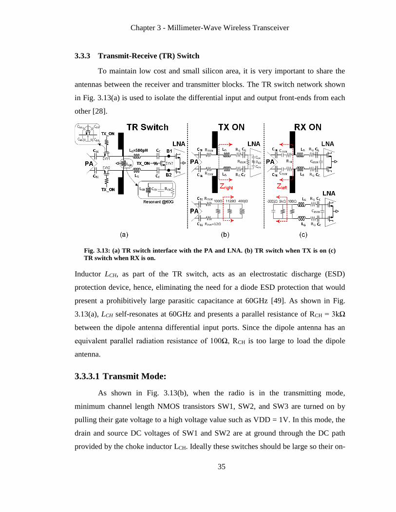
Chapter 3 - Millimeter-Wave Wireless Transceiver
35
3.3.3 Transmit-Receive (TR) Switch
To maintain low cost and small silicon area, it is very important to share the
antennas between the receiver and transmitter blocks. The TR switch network shown
in Fig. 3.13(a) is used to isolate the differential input and output front-ends from each
other [28].
Fig. 3.13: (a) TR switch interface with the PA and LNA. (b) TR switch when TX is on (c)
TR switch when RX is on.
Inductor LCH, as part of the TR switch, acts as an electrostatic discharge (ESD)
protection device, hence, eliminating the need for a diode ESD protection that would
present a prohibitively large parasitic capacitance at 60GHz [49]. As shown in Fig.
3.13(a), LCH self-resonates at 60GHz and presents a parallel resistance of RCH = 3kΩ
between the dipole antenna differential input ports. Since the dipole antenna has an
equivalent parallel radiation resistance of 100Ω, RCH is too large to load the dipole
antenna.
3.3.3.1 Transmit Mode:
As shown in Fig. 3.13(b), when the radio is in the transmitting mode,
minimum channel length NMOS transistors SW1, SW2, and SW3 are turned on by
pulling their gate voltage to a high voltage value such as VDD = 1V. In this mode, the
drain and source DC voltages of SW1 and SW2 are at ground through the DC path
provided by the choke inductor LCH. Ideally these switches should be large so their on-

Chapter 3 - Millimeter-Wave Wireless Transceiver
36
resistance, RTSW, become much smaller than the antenna impedance. But, in the
receiving mode, it is desirable to minimize the source-drain capacitances of SW1 and
SW2. So an optimum switch size of (32µm/40nm) is chosen to satisfy both cases. This
switch size is large enough to meet the metal electro-migration rule for at least 20mA
of DC current. The parasitic model of SW1 is shown in Fig. 3.13(a). Other switches
have the same parasitic model. It is important to use a large resistor, for example, 5kΩ,
at the gates of SW1 and SW2 so their gate-source and gate-drain capacitances would
not load the PA. For SW3, the drain and source voltages are also pulled to ground
through a biasing network that pulls the voltage at nodes B1 and B2 to ground. As
shown in Fig. 3.13(b), when SW3 is on, the differential impedance on the right seen at
the differential terminals of the dipole antenna is:
𝑍𝑟𝑖𝑔ℎ𝑡 = 2𝐿𝐺𝜔𝑗 + 2𝑅𝐺 +
2
𝐶𝐶𝜔𝑗+ 𝑅𝑅𝑆𝑊|| (
2
𝐶𝐺𝑆𝜔𝑗+ 𝑅𝐺𝑆),
(3.6)
where RRSW is the on-resistance of SW3, RG is the parasitic resistance of gate
inductance LG, Rgs and Cgs are the parasitic resistance and capacitance of the LNA
input, and CC=220fF is an AC coupling cap. With an SW3 size of (4µm/40nm), the
overall impedance of 2𝑗
𝐶𝐶𝜔+ 𝑅𝑅𝑆𝑊|| (
2
𝐶𝐺𝑆𝜔𝑗+ 𝑅𝐺𝑆) equals (78 +
1
(72𝑓𝐹)𝜔𝑗) Ω. With LG
= 580pH and a quality factor of 5, 𝑍𝑟𝑖𝑔ℎ𝑡 = 1129Ω||400𝑗Ω at 60GHz. The simplified
equivalent circuit for Zright and the dipole parallel differential resistance of 100Ω is
shown in Fig. 3.13(b). The effective impedance seen by the PA is:
100Ω||1129Ω||400𝑗Ω = 91Ω||400𝑗Ω. (3.7)
The imaginary part of (3.7) can be absorbed by the PA matching network.
Therefore, the TR switch loss due to the loading of the LNA is:10 log(91Ω/100Ω) =
−0.85𝑑𝐵. An extra simulated loss of 1dB is due to the on-resistance of SW1/SW2. So
the total TR switch loss is -1.85dB.
3.3.3.2 Receive Mode:
As shown in Fig. 3.13(c), in receive mode, NMOS transistors SW1, SW2, and
SW3 are turned off by pulling their gate voltages to ground. The drain and source
voltages of SW1 and SW2 are DC-coupled to ground through LCH. When turned off,

Chapter 3 - Millimeter-Wave Wireless Transceiver
37
SW1 and SW2 present an effective parasitic drain-source capacitance, CTSW, and an
effective parasitic series resistance, RTX. As shown in Fig. 3.13(c), looking at the left
of the dipole antenna, simulated at 60GHz, the effective impedance is lower bounded
as:
𝑍𝑙𝑒𝑓𝑡 > 2𝑅𝑇𝑋 +
2
𝐶𝑇𝑆𝑊𝜔𝑗= (36.3 − 328𝑗)Ω
= 3𝑘Ω||(−332𝑗)Ω
(3.8)
Therefore, the effective antenna impedance seen by the PA is lower bounded
by: 100Ω||𝑍𝑙𝑒𝑓𝑡 = 97Ω||(−332𝑗)Ω. The imaginary part of (3.8) can be absorbed by
the LNA input matching network. The loss due to the TR switch during RX on is
therefore:10 log(97Ω/100Ω) = −0.3𝑑𝐵.
3.4 Receiver Design
The receiver architecture is shown in Fig. 3.14. There are two LNAs for the
two dipole antennas. Each LNA consists of two stages that are coupled by
transformers. The third stage is common between the two paths and sums the output
voltages of the two LNAs. This summing improves the receiver sensitivity by 3 dB. It
also provides additional 6 dB of voltage gain. A common source amplifier is used for
the LNA's front-end stage. The choice is partially driven by the fact that the antenna is
being shared between the LNA and PA. In this case, the overall link budget was
improved as the common source LNA improved the TR switch loss in transmit mode.
There are two other reasons for using a common source LNA.
First, for the same power consumption, inductor degeneration reduces the gain
of the first stage, increasing the noise figure (NF) contribution of the later stages. In
this design, the NF of the self-mixing stage and the chain of the baseband amplifiers is
significantly higher than the LNA. Therefore, it is best to have the highest gain at the
LNA stages as the noise contribution of the post LNA stages will be divided by the
overall LNA gain.
Second, for low power LNA design, where the input NMOS transistors are
small, the effective resistance of the NMOS input transistor in series with its gate

Chapter 3 - Millimeter-Wave Wireless Transceiver
38
capacitance is sizable compared to the antenna radiation resistance. At an operating
gate voltage of 0.7 V, the series gate resistance and capacitance of a differential
NMOS pair are 67 Ω and 6.1 fF ( 33.5 Ω and 12.2 fF single-ended). This impedance
should be matched to a 100 Ω differential antenna. A gate inductance, LG, of 580 pH
resonates out the gate capacitance at 60 GHz. With a Q of 5, the parasitic series
resistance of LG equals 43 Ω. Therefore, the total impedance seen by the antenna at 60
GHz is 67 Ω + 2 × 43 Ω = 153 Ω. This results in an S11 of lower than -10 dB.
Fig. 3.15 shows the simulation results for the LNA NF, gain and S11. The
return loss, S11, maintains lower than -10 dB from 52 GHz to 66 GHz. The NF is
below 6 dB from 54 GHz to 66 GHz with a minimum of 5.2 dB at around 60 GHz.
The maximum overall gain of the two LNAs is 40.5 dB simulated at the output of the
voltage summation circuit at above 60 GHz. Each LNA path has a simulated gain of
34.5 dB. The first, second and third LNA stages have voltage gains of 10.6 dB, 11.5
dB, and 9.4 dB. There is additional 3 dB gain due to the input matching Q boosting.
All input transistors of the LNA stages are biased by a 3 bit resistor DAC. The cascode
transistors are biased to the voltage supply. The total power consumption of the two
LNAs is programmable from 38 mW to 72 mW. The simulated NF was achieved at a
48 mW total power consumption.
As shown in Fig. 3.14, each LNA stage included stacked cross-coupled NMOS
transistors to provide negative resistance. This was intended to boost the LNA gain.
As explained earlier, the NF of the receiver chain is largely dominated by the envelope
detector mixer and the following BB amplifiers, so maximizing the gain of the LNA
stages results in the lowest overall NF. However, during the measurement, the
negative resistance caused oscillations so the cross-coupled NMOS were kept off.

Chapter 3 - Millimeter-Wave Wireless Transceiver
39
Fig. 3.14: Receiver chain (RF and BB).
The output of the voltage summation stage feeds a passive AC-coupled self-
mixer to extract the OOK modulation envelope, as shown in Fig. 3.14. The drain and
source bias voltage for the mixer transistors is provided by the self-biased inverter that
follows the mixer. The gate bias is at one threshold voltage above the source-drain
voltage. This ensures the transistors are biased at near threshold for maximum RF to
BB gain. Because of the non-linear nature of the envelope detector mixer, its NF is a
very strong function of the RF input voltage. The receiver baseband is a 3-stage DC-
coupled inverter chain with resistive feedback followed by a common-source amplifier
with programmable resistive load. The last stage drives an external 50 Ω load, for
example, an oscilloscope.

Chapter 3 - Millimeter-Wave Wireless Transceiver
40
Fig. 3.15: Simulated NF, gain and return loss of the LNA.
Fig. 3.16: Total NF of RX chain vs. LNA input power.
Fig. 3.16 shows the integrated noise figure of the total RX chain over the
signal bandwidth of interest versus the input signal power to the LNA. The integrated
NF (10 kHz to 8 GHz) of the receiver including the mixer and the baseband chain is

Chapter 3 - Millimeter-Wave Wireless Transceiver
41
31 dB in simulations when the RF input at 60 GHz is at the sensitivity level. The
overall receiver NF is overwhelmed by the mixer and the BB chain. Because of the
very non-linear nature of the mixer, the integrated noise figure is a very strong
function of the input signal power. The VCOs in the TX were measured to oscillate at
around 56.5 GHz, as a result of extra parasitics that were not captured in simulations.
Therefore, the LNA gain at this frequency is 10 dB lower than its intended peak at 60
GHz. As a result, the overall RX NF is worse than expected.
3.5 Dipole Antenna
At mm-wave frequencies, on-chip antennas become a viable option as the
wavelength is comparable to the die size of a complex transceiver design [50], [51],
[52], [53]. Furthermore, on-chip antennas eliminate the loss due to the interconnect
techniques such as wire-bond, wafer-level-packaging (WLP), ball-grid-array (BGA),
and so on. However, the low resistivity of the silicon substrate (10Ω-cm) introduces
electric field losses leading to a reduction in antenna efficiency and radiation
resistance. Also, the high permittivity of the silicon substrate (εr = 11.9) results in the
absorption of the fields in the substrate thus giving rise to undesirable substrate modes
that adversely impacts the antenna efficiency [54], [55]. The two most commonly used
techniques to improve antenna efficiency involve using a substrate dielectric lens [50],
[56] and substrate thinning [42], [53], [57]. The di-electric lens is large, expensive,
and needs accurate placement with respect to the on-chip antenna. On the other hand,
die thinning is a one-time process and can be performed at the wafer-level to reduce
the cost for mass fabrication.
The implemented on-chip antennas are shown in Fig. 3.17. They consists of
two dipole elements on top of aluminum layer with a separation of 0.12 λ, where
λ=5mm is the free space wavelength at 60 GHz. The assumption for the mm-Wave
radios with off-chip antenna arrays is that the antenna spacing is 0.5 λ. One concern in
choosing the appropriate antenna spacing is the mutual coupling between the antennas.
It is defined as the ratio of the power received from one antenna to the power that the
other antenna is transmitting. This mutual coupling is typically undesirable as the

Chapter 3 - Millimeter-Wave Wireless Transceiver
42
power that should be transmitted is wasted as the result of absorption in another
antenna. It could also change the pattern of each individual antenna. Furthermore, a
high coupling between the adjacent antennas could exacerbate the voltage wave
standing ratio (VWSR) in the transmitter PA. The VSWR at the output of the PA
needs to be as small as possible for two reasons. The first reason is the reliability of
the CMOS devices. CMOS transistors have a reliability voltage guideline. Exceeding
these limits would either destroy the device or reduce its lifetime. The second reason is
to minimize the error vector magnitude (EVM). The EVM is the inverse of the SNR
and factors such as noise, linearity and mismatch could degrade it. A large VSWR
appears at the PA output and makes it nonlinear, hence increasing the EVM. On the
receiver side, the mutual coupling would make the inputs correlated. The correlation
adversely affects the array beamforming and resolution.
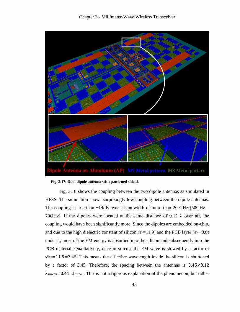
Chapter 3 - Millimeter-Wave Wireless Transceiver
43
Fig. 3.17: Dual dipole antenna with patterned shield.
Fig. 3.18 shows the coupling between the two dipole antennas as simulated in
HFSS. The simulation shows surprisingly low coupling between the dipole antennas.
The coupling is less than −14dB over a bandwidth of more than 20 GHz (50GHz –
70GHz). If the dipoles were located at the same distance of 0.12 λ over air, the
coupling would have been significantly more. Since the dipoles are embedded on-chip,
and due to the high dielectric constant of silicon (𝜖𝑟=11.9) and the PCB layer (𝜖𝑟=3.8)
under it, most of the EM energy is absorbed into the silicon and subsequently into the
PCB material. Qualitatively, once in silicon, the EM wave is slowed by a factor of
√𝜖𝑟=11.9=3.45. This means the effective wavelength inside the silicon is shortened
by a factor of 3.45. Therefore, the spacing between the antennas is 3.45×0.12
𝜆𝑠𝑖𝑙𝑖𝑐𝑜𝑛=0.41 𝜆𝑠𝑖𝑙𝑖𝑐𝑜𝑛. This is not a rigorous explanation of the phenomenon, but rather

Chapter 3 - Millimeter-Wave Wireless Transceiver
44
an intuitive and easy to understand qualitative explanation. It is very desirable to be
able to place the array antennas very close to each other, without suffering from
excessive coupling between them.
Fig. 3.18: HFSS simulation for antenna to antenna coupling.
To meet the metal density rule, a patterned floating shield on the two top
copper metal layers was placed below the dipole antennas, as shown in Fig. 3.17. The
area under the shield is used for digital circuits as well as energy storing capacitors for
the harvest block. To minimize the loss due to the substrate, the dipole elements were
placed very close to the edge of the chip [58], and the silicon was thinned to 100μm
[55]. At 60 GHz, λ0 = 5 mm, and with ℎ= 100 μm, ℎ/λ0 = 0.02. This is well within the
suggested range illustrated in Fig. 3.19.

Chapter 3 - Millimeter-Wave Wireless Transceiver
45
Fig. 3.19: Impact of substrate thickness on antenna gain and normalized power [54].
Furthermore, a metal reflector was placed at a distance of quarter wavelength
from the antenna. Simulations suggest that metal reflector improves the overall
antenna gain by about 4dB (Fig. 3.20), which was also noticed in the measurement, as
shown in Fig. 3.21. The antenna gain is a measure of how much of the
transmitted/received power is concentrated in a particular direction. Intuitively, the
electromagnetic waves are blocked from radiating or passing through the metal
reflector. Thus the half-space behind the metal reflector has no EM power in it and the
half-space in front of it has twice as much power and hence, ideally a 3 dB gain
improvement. This theoretical 3 dB gain improvement can also be explained by
method of images and would be discussed in next section. The radiation patterns for
the dual dipole antennas and the single dipole antenna are shown in Fig. 3.20 with and
without the metal reflector.
The simulated S11 from HFSS indicates a bandwidth of greater than 20GHz as
shown in Fig. 3.22. The silicon chip with the dipole antennas sits over a FR4 PCB
material. The PCB is 600μm thick. The radiation is taken from the PCB side. This is
because the electromagnetic fields tend to go through the materials with higher
dielectric constant than that of air. The choice of the FR4 material is due to its lower
cost. There are other PCB materials with lower loss at 60-GHz but are more expensive

Chapter 3 - Millimeter-Wave Wireless Transceiver
46
and hence not so desirable for low cost and mass markets. The overall efficiency of
the dipole antenna over the PCB is 50.11%. For silicon the dielectric constant and the
loss tangent is assumed to be 11.9 and 0.65 respectively. For the PCB, the dielectric
constant and loss tangent is 3.8 and 0.02 respectively [59].
Fig. 3.20: Simulated radiation pattern (a) Dual dipole with metal reflector. (b) Dual dipole
without metal reflector. (c) Single dipole with metal reflector. (d) Single dipole without
metal reflector.
Fig. 3.21: Normalized measured radiation patterns (a) Elevation (b) Azimuth.
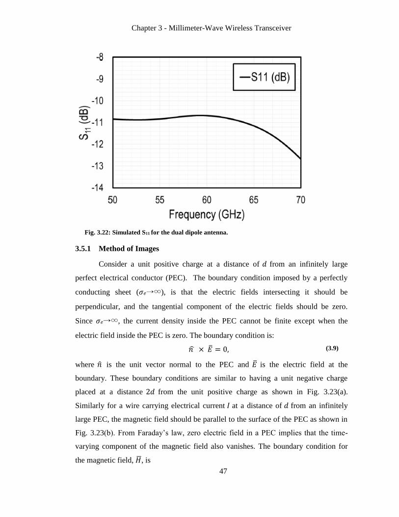
Chapter 3 - Millimeter-Wave Wireless Transceiver
47
Fig. 3.22: Simulated S11 for the dual dipole antenna.
3.5.1 Method of Images
Consider a unit positive charge at a distance of 𝑑 from an infinitely large
perfect electrical conductor (PEC). The boundary condition imposed by a perfectly
conducting sheet (𝜎𝑒→∞), is that the electric fields intersecting it should be
perpendicular, and the tangential component of the electric fields should be zero.
Since 𝜎𝑒→∞, the current density inside the PEC cannot be finite except when the
electric field inside the PEC is zero. The boundary condition is:
𝑛 × = 0, (3.9)
where is the unit vector normal to the PEC and is the electric field at the
boundary. These boundary conditions are similar to having a unit negative charge
placed at a distance 2𝑑 from the unit positive charge as shown in Fig. 3.23(a).
Similarly for a wire carrying electrical current 𝐼 at a distance of 𝑑 from an infinitely
large PEC, the magnetic field should be parallel to the surface of the PEC as shown in
Fig. 3.23(b). From Faraday’s law, zero electric field in a PEC implies that the time-
varying component of the magnetic field also vanishes. The boundary condition for
the magnetic field, , is
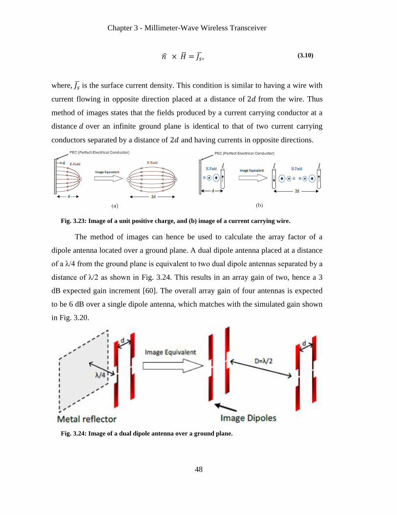
Chapter 3 - Millimeter-Wave Wireless Transceiver
48
𝑛 × = 𝐽 , (3.10)
where, 𝐽 is the surface current density. This condition is similar to having a wire with
current flowing in opposite direction placed at a distance of 2𝑑 from the wire. Thus
method of images states that the fields produced by a current carrying conductor at a
distance 𝑑 over an infinite ground plane is identical to that of two current carrying
conductors separated by a distance of 2𝑑 and having currents in opposite directions.
Fig. 3.23: Image of a unit positive charge, and (b) image of a current carrying wire.
The method of images can hence be used to calculate the array factor of a
dipole antenna located over a ground plane. A dual dipole antenna placed at a distance
of a λ/4 from the ground plane is equivalent to two dual dipole antennas separated by a
distance of λ/2 as shown in Fig. 3.24. This results in an array gain of two, hence a 3
dB expected gain increment [60]. The overall array gain of four antennas is expected
to be 6 dB over a single dipole antenna, which matches with the simulated gain shown
in Fig. 3.20.
Fig. 3.24: Image of a dual dipole antenna over a ground plane.

Chapter 3 - Millimeter-Wave Wireless Transceiver
49
3.6 Energy Harvesting Circuit design
The energy harvesting circuit uses four stages of cascaded CMOS rectifiers as
shown in Fig. 3.25 [61]. The input of the rectifier is connected to a loop antenna on the
PCB through a shunt-series capacitor matching network that harvests RF energy at
2.45 GHz. The impedance looking into the harvesting circuit varies as a function of
the RF input power. This design uses a fixed off-chip matching network for all levels
of the input RF power. Therefore, for some RF input powers, the harvesting efficiency
is not optimized because of the impedance mismatch. The output of the four-stage
CMOS rectifier is connected to an on-chip 3 nF capacitor for energy storage. With
four stages of rectification, a nominal output voltage in excess of 1.1 V is achieved.
Each rectifier stage consists of two NMOS/PMOS transistor pairs which are
successively turned on and off by the incoming RF sinusoid thereby pumping the
charge to the storage cap.
Fig. 3.25: Energy harvesting front-end circuit.
Since the rectifier output voltage can vary with 2.45 GHz RF input power level
as well as load current, a supply detection mechanism is necessary. This is to ensure
that the supply remains at a level high enough for the transmitter to operate properly.
Fig. 3.26(a) shows the supply detection mechanism state diagram. The transmitter
turns on when the harvested supply has reached 1.1 V and keeps transmitting until the
supply falls below 0.8 V, as shown in Fig. 3.26(b). This hysteresis allows sufficient
time for transmit operation, before the supply drops below the 0.8 V level due to the
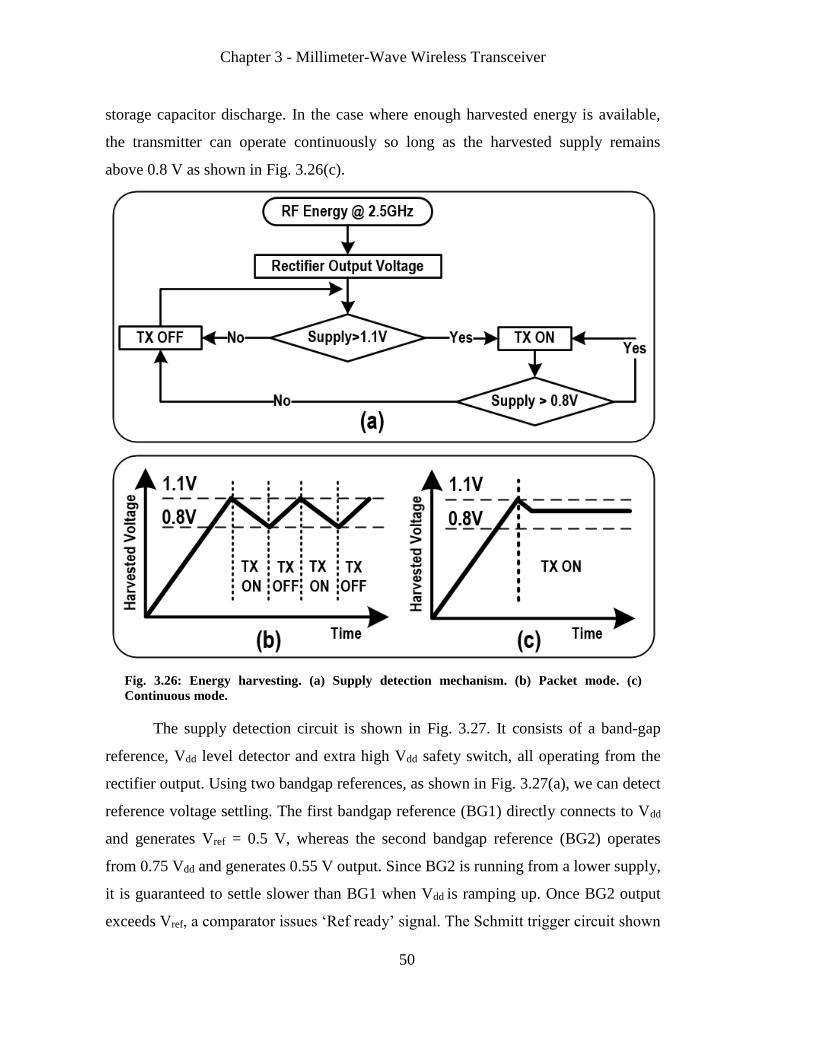
Chapter 3 - Millimeter-Wave Wireless Transceiver
50
storage capacitor discharge. In the case where enough harvested energy is available,
the transmitter can operate continuously so long as the harvested supply remains
above 0.8 V as shown in Fig. 3.26(c).
Fig. 3.26: Energy harvesting. (a) Supply detection mechanism. (b) Packet mode. (c)
Continuous mode.
The supply detection circuit is shown in Fig. 3.27. It consists of a band-gap
reference, Vdd level detector and extra high Vdd safety switch, all operating from the
rectifier output. Using two bandgap references, as shown in Fig. 3.27(a), we can detect
reference voltage settling. The first bandgap reference (BG1) directly connects to Vdd
and generates Vref = 0.5 V, whereas the second bandgap reference (BG2) operates
from 0.75 Vdd and generates 0.55 V output. Since BG2 is running from a lower supply,
it is guaranteed to settle slower than BG1 when Vdd is ramping up. Once BG2 output
exceeds Vref, a comparator issues ‘Ref ready’ signal. The Schmitt trigger circuit shown

Chapter 3 - Millimeter-Wave Wireless Transceiver
51
in Fig. 3.27(b) is responsible for the supply level detection. The ‘Vdd ready’ output of
the comparator is asserted whenever 0.8 V < Vdd < 1.1 V. The circuit shown in Fig.
3.27(c) applies a leakage load current to the supply whenever Vdd exceeds 1.3 V. This
is to lower the harvested VDD voltage for the case when too much harvested energy is
available and the supply voltage is outside the reliability region.
Fig. 3.27: Supply detection. (a) Bandgap reference. (b) Vdd level detection. (c) Extra high
Vdd safety switch.
3.7 Measurements
A 0.9×1.8mm2 chip, including two on-chip dipole antennas, was fabricated in
TSMC 40nm GP technology with 9 metal layers. Two different versions of the chip
were fabricated with different baseband circuits. The first version focused on
achieving ultra-low power operation for NFC communication and was tested using
harvested energy on the transmitter side. For the second version of the chip, the digital
baseband was redesigned to meet the requirements of wireless MRI systems. As a
result, second version has more pins as compared to the first version. This version
was tested using non-magnetic batteries and its performance inside the MRI would be
discussed in detail in the next chapter. The RF performance of both the versions was
similar and the die micrographs are shown in Fig. 3.28.

Chapter 3 - Millimeter-Wave Wireless Transceiver
52
Fig. 3.28: Die photo (a) first version for NFC application, (b) the second version for
wireless MRI application. The silicon is 1.8 mm × 0.9 mm for both versions.
Fig. 3.29: (a) Metal reflector facing the front-side. The radiation is through the PCB on the
back-side. (b) The plastic fixture used to hold the metal reflector. The harvest antenna
connector ports into the chip. (c) The silicon radio wire-bonded on a FR4 PCB material.
All the measurements include the metal reflector shown in Fig. 3.29 for both
the RX and TX. With NFC as the primary application, the transmitter and receiver
were placed at two distances of 5 and 10cm, as shown in Fig. 3.30(a) and (b). In all

Chapter 3 - Millimeter-Wave Wireless Transceiver
53
link measurements, the transmitter energy was harvested at 2.45GHz using a loop
antenna differentially connected through an impedance matching network to the on-
chip harvesting circuit as shown in Fig. 3.25. Since the 5cm and 10cm links have
different power consumptions, the on-chip loading seen by the harvest loop antenna is
not constant. For some on-chip loading conditions the power transfer and hence
harvest efficiency (η) is near the optimum value. Since we used the same matching
network for all loading conditions, η changes as a function of the TX power
consumption. η was measured using the setup shown in Fig. 3.30(a) and measured η of
the matching network, PCB interconnects and the 4-stage CMOS rectifier is shown in
Fig. 3.31(a). The RF power source used for energy harvesting is a signal generator at
2.45GHz, which feeds a loop antenna that radiates RF energy to the harvesting loop
antenna that is connected to the harvesting block through off-chip impedance
matching.
The harvested power was measured by probing the voltage of the supply pin at
the storage cap, Cstorage, as shown in Fig. 3.25, using an oscilloscope. For example, at a
certain data rate the oscilloscope measured a harvested voltage of 0.9V. We could
deduce the TX average DC power consumption by disconnecting the harvesting
antenna and instead providing a DC power supply of 0.9V at the same pin that was
probed by the oscilloscope. Now we can easily measure the DC power consumption
by reading the DC current through the 0.9V supply. This would be identical to the
power obtained by harvesting that resulted in a 0.9V supply. The loss, Lharvest, between
the harvest antenna of the transmitter and the RF power source antenna was measured
to be 10dB and 8dB at 10cm and 5cm respectively. Therefore, the RF power needed at
2.45GHz at the source loop antenna to provide an average DC power of Ptx (dBm) for
the transmitter operation is:
𝑃RF_Source = 𝑃𝑡𝑥(dBm) +
1
η(dB) + 𝐿ℎ𝑎𝑟𝑣𝑒𝑠𝑡.
(3.
11)
For example, for a transmitter average DC power consumption of 1 mW (0
dBm), by looking at Fig. 3.31(a), the harvest efficiency is approximately 30% (- 4.5dB)
and therefore an RF source power of 14.5 and 12.5 dBm for 10 and 5 cm distance is

Chapter 3 - Millimeter-Wave Wireless Transceiver
54
required. This power can be readily available from the PAs in handheld devices with
WLAN capabilities operating at ISM band of 2.45GHz [62].
Fig. 3.30: Measurement setup (a) Harvesting efficiency. (b) BER. (c) Pulse-width. (d)
Coherent time.
Fig. 3.31: (a) Harvest efficiency. (b) TX power vs. data rate. (c) Bit-error rate vs. data rate.
For the BER measurements, the transmitter and receiver were aligned at the
broadside direction of their respective dual-dipole, as shown in Fig. 3.30(b). A 127-bit
on-chip pseudo random bit sequence (PRBS) generator was used to generate 38Mb/s
to 2450Mb/s data stream with 6-bit programmable (N=0, … ,5) divide by 2N. For a
BER < 5×10⁻⁵, the two-element transmitter consumes 260µW to 11.9mW at a distance
of 10cm. At 5cm, a BER < 5×10⁻⁴ was achieved by turning on only one transmit

Chapter 3 - Millimeter-Wave Wireless Transceiver
55
element, which consumes 100µW to 6.3mW. Fig. 3.31(b) shows the linear relationship
between power and data rate for 5cm and 10cm distances. The receiver, including the
baseband drivers, consumes 74mW. The BER was measured by saving the receiver
baseband output to an Agilent DSA90804A oscilloscope and processing the data in
Matlab. Fig. 3.31(c) shows the measured BER for different data rates at 5cm and 10cm
distances. An eye-diagram view of the received baseband pulses is shown in Fig. 3.32.
Since the clock recovery was not implemented on-chip, the 2.45GHz clock from the
RF power source was directly fed into the oscilloscope. In addition to the oscilloscope,
an Agilent N4903B J-BERT was used to perform BER measurement. Since J-BERT
had a built-in clock recovery, there was no need to provide an external clock.
Fig. 3.32: Oscilloscope eye diagram at 2.45 Gb/s at 10 cm (voltage scale: 100 mV/div, time
scale: 100 ps/div).
Fig. 3.30 (c) shows the measurement setup of the power spectral density of the
PRBS signal. The TX carrier frequency is around 56.5GHz. Fig. 3.33 shows an
approximate sinc function with a BW of 3.5GHz. This corresponds to a pulse width of
570ps. The next maxima on the left is 13dB lower in power which matches that of an
ideal sinc function. This is not the case for the maxima on the right, and that is because
of extra losses of the cables and the down-converter at higher frequencies. The

Chapter 3 - Millimeter-Wave Wireless Transceiver
56
measurement confirms the nearly rectangular envelope of the 60GHz signal. Narrower
pulse widths were also measured, and the increased BW could be seen, but due to the
limitations of the measurement setup they did not compare well with sinc function
created with wider pulse widths.
Fig. 3.33: Power spectral density of a long PRBS.
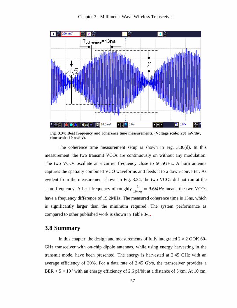
Chapter 3 - Millimeter-Wave Wireless Transceiver
57
Fig. 3.34: Beat frequency and coherence time measurements. (Voltage scale: 250 mV/div,
time scale: 10 ns/div).
The coherence time measurement setup is shown in Fig. 3.30(d). In this
measurement, the two transmit VCOs are continuously on without any modulation.
The two VCOs oscillate at a carrier frequency close to 56.5GHz. A horn antenna
captures the spatially combined VCO waveforms and feeds it to a down-converter. As
evident from the measurement shown in Fig. 3.34, the two VCOs did not run at the
same frequency. A beat frequency of roughly 1
104𝑛𝑠= 9.6𝑀𝐻𝑧 means the two VCOs
have a frequency difference of 19.2MHz. The measured coherence time is 13ns, which
is significantly larger than the minimum required. The system performance as
compared to other published work is shown in Table 3-1.
3.8 Summary
In this chapter, the design and measurements of fully integrated 2 × 2 OOK 60-
GHz transceiver with on-chip dipole antennas, while using energy harvesting in the
transmit mode, have been presented. The energy is harvested at 2.45 GHz with an
average efficiency of 30%. For a data rate of 2.45 Gb/s, the transceiver provides a
BER < 5 × 10⁻⁴ with an energy efficiency of 2.6 pJ/bit at a distance of 5 cm. At 10 cm,
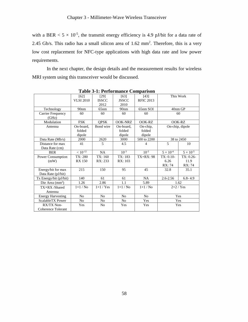
Chapter 3 - Millimeter-Wave Wireless Transceiver
58
with a BER < 5 × 10⁻⁵, the transmit energy efficiency is 4.9 pJ/bit for a data rate of
2.45 Gb/s. This radio has a small silicon area of 1.62 mm2. Therefore, this is a very
low cost replacement for NFC-type applications with high data rate and low power
requirements.
In the next chapter, the design details and the measurement results for wireless
MRI system using this transceiver would be discussed.
Table 3-1: Performance Comparison [62]
VLSI 2010
[29]
ISSCC
2012
[63]
JSSCC
2010
[43]
RFIC 2013
This Work
Technology 90nm 65nm 90nm 65nm SOI 40nm GP
Carrier Frequency
(GHz)
60 60 60 60 60
Modulation FSK QPSK OOK-NRZ OOK-RZ OOK-RZ
Antenna On-board,
folded
dipole
Bond wire On-board,
folded
dipole
On-chip,
folded
dipole
On-chip, dipole
Data Rate (Mb/s) 2000 2620 3000 500 to 2200 38 to 2450
Distance for max
Data Rate (cm)
41 5 4.5 4 5 10
BER < 10-12 NA 10-3 10-5 5 × 10⁻⁴ 5 × 10⁻⁵
Power Consumption
(mW)
TX: 280
RX 150
TX: 160
RX: 233
TX: 183
RX: 103
TX+RX: 98 TX: 0.10-
6.26
RX: 74
TX: 0.26-
11.9
RX: 74
Energy/bit for max
Data Rate (pJ/bit)
215 150 95 45 32.8 35.1
Tx Energy/bit (pJ/bit) 140 61 61 NA 2.6-2.56 6.8- 4.9
Die Area (mm2) 1.26 2.86 1.1 5.89 1.62
TX×RX /Shared
Antenna
1×1 / No 1×1 / Yes 1×1 / No 1×1 / No 2×2 / Yes
Energy Harvesting No No No No Yes
ScalableTX Power No No No Yes Yes
RX/TX Non-
Coherence Tolerant
Yes No Yes Yes Yes
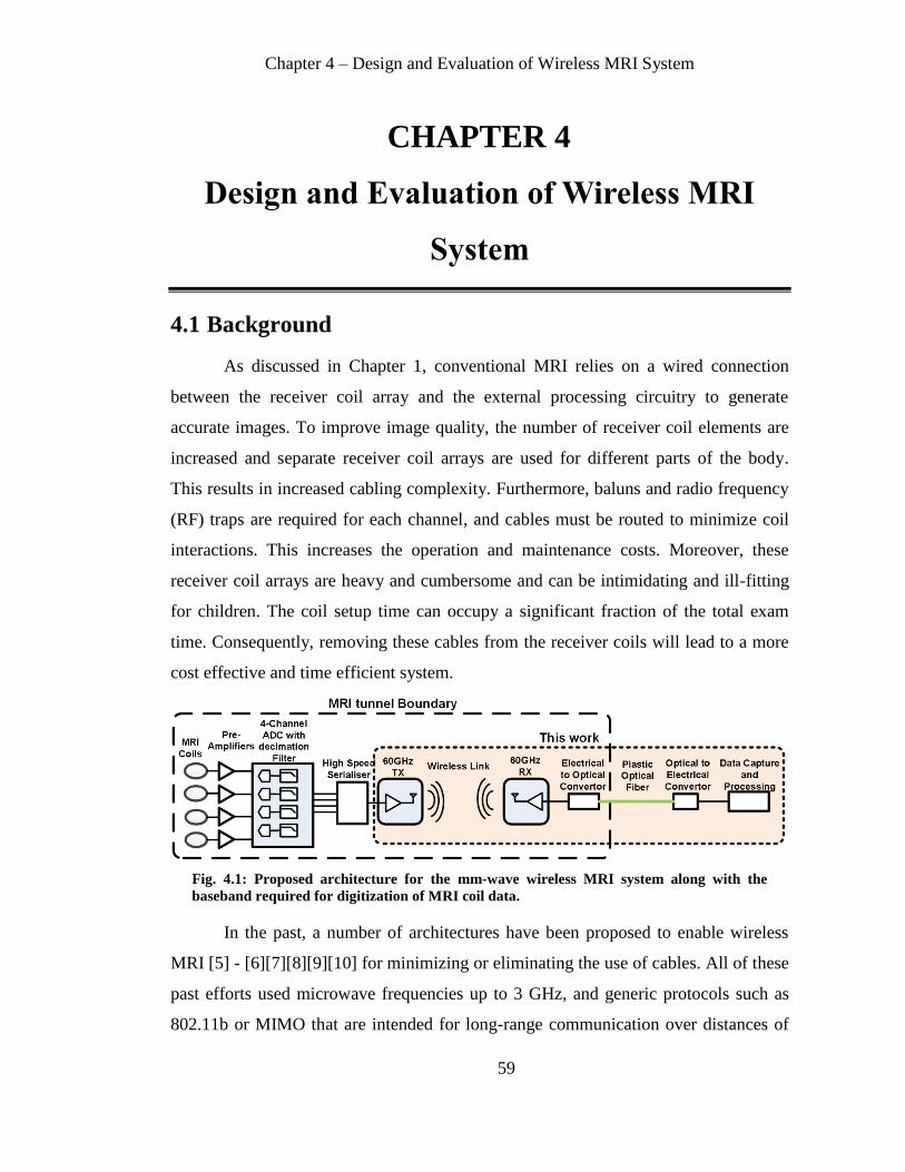
Chapter 4 – Design and Evaluation of Wireless MRI System
59
CHAPTER 4
Design and Evaluation of Wireless MRI
System
4.1 Background
As discussed in Chapter 1, conventional MRI relies on a wired connection
between the receiver coil array and the external processing circuitry to generate
accurate images. To improve image quality, the number of receiver coil elements are
increased and separate receiver coil arrays are used for different parts of the body.
This results in increased cabling complexity. Furthermore, baluns and radio frequency
(RF) traps are required for each channel, and cables must be routed to minimize coil
interactions. This increases the operation and maintenance costs. Moreover, these
receiver coil arrays are heavy and cumbersome and can be intimidating and ill-fitting
for children. The coil setup time can occupy a significant fraction of the total exam
time. Consequently, removing these cables from the receiver coils will lead to a more
cost effective and time efficient system.
Fig. 4.1: Proposed architecture for the mm-wave wireless MRI system along with the
baseband required for digitization of MRI coil data.
In the past, a number of architectures have been proposed to enable wireless
MRI [5] - [6][7][8][9][10] for minimizing or eliminating the use of cables. All of these
past efforts used microwave frequencies up to 3 GHz, and generic protocols such as
802.11b or MIMO that are intended for long-range communication over distances of

Chapter 4 – Design and Evaluation of Wireless MRI System
60
10 m to 100 m. Such generic long range communication protocols are sub-optimal
solutions for wireless MRI in terms of power consumption and size. This is because
typical MRI bore diameters vary from 60 cm to 70 cm. And, depending on a patient’s
physical attributes and the part of the body to be imaged, the distance between the coil
array and the magnet bore/edge can vary from 10 cm to 50 cm.
In this work, we propose a custom millimeter (mm) wave transceiver
architecture that is specifically designed to meet the requirements of wireless MRI
data rates while minimizing power consumption and size. A block diagram is shown
in Fig. 4.1 in which the mm wave radio provides a short-range (10-50 cm) link within
the MRI bore, and a fiber optic link transports data beyond the magnet to the console
for image reconstruction. The mm-wave data transmitter (TX) is located on the MRI
receiver coil assembly and the mm-wave data receiver (RX) is embedded inside the
MRI system bore. With the on-chip dipole antennas, the designed 60-GHz radio
achieves a raw bit error rate (BER) of 10-6 for a distance of 10 cm, which is much
better than the raw BER specification of 10-2 for a typical WiFi, 802.11n system [64],
[65], or 10-3 for a Bluetooth system [66]. For a TX-RX separation of 50 cm, the
receiver is coupled with an external horn antenna and an LNA to compensate for
higher signal loss at a longer transmission distance.
4.2 System Design Challenges
The static magnetic field inside the MRI bore tube (~1.5T) is ten thousand
times stronger than the earth’s magnetic field. As a result, any magnetic material in the
vicinity of the MRI bore tube experiences a very strong magnetic pull and may even
damage the MRI machine as illustrated in Fig. 4.2. Thus designing a system for an
MRI room poses certain challenges that are normally not encountered in a normal lab
environment. For example:
Power Supplies: Conventional power supplies cannot be used inside the
MRI room as their consoles are made up of iron/steel which are highly
magnetic. The proposed MRI system solves this problem by using non-
magnetic batteries (PowerStream - PGEB-NMO53040).

Chapter 4 – Design and Evaluation of Wireless MRI System
61
Metallic Board Holders: During the initial evaluation phase of a system in
a lab, metallic holders are used to hold the test boards of the design as
shown in Fig. 4.3(a). Typically, these holders are made out of iron/steel
and hence can’t be used inside the MRI room. This was resolved by
designing a custom holder made up of Lego® bricks which is MRI safe as
shown in Fig. 4.3(b).
Proximity between Oscilloscopes and Design under Test (DUT): To
evaluate a system’s true performance, it is desirable to minimize the
distance between the measurement equipment such as an oscilloscope and
the design under test. Commercially available oscilloscopes can’t be taken
inside the MRI room because they have iron/steel enclosures. As a
consequence, the distance between the DUT placed inside the MRI bore
tube and the measurement equipment in the MRI console room is ~5 m.
Signal transmission over such long distances using standard SMA cables
results in a high transmission loss which is undesirable. Furthermore,
magnetic field gradients inside the MRI room might corrupt the signal. To
address these issues, a fiber optic transceiver (Firecomms 1Gbps LC
transceiver) system is used to transfer data between the DUT and the
measurement equipment.
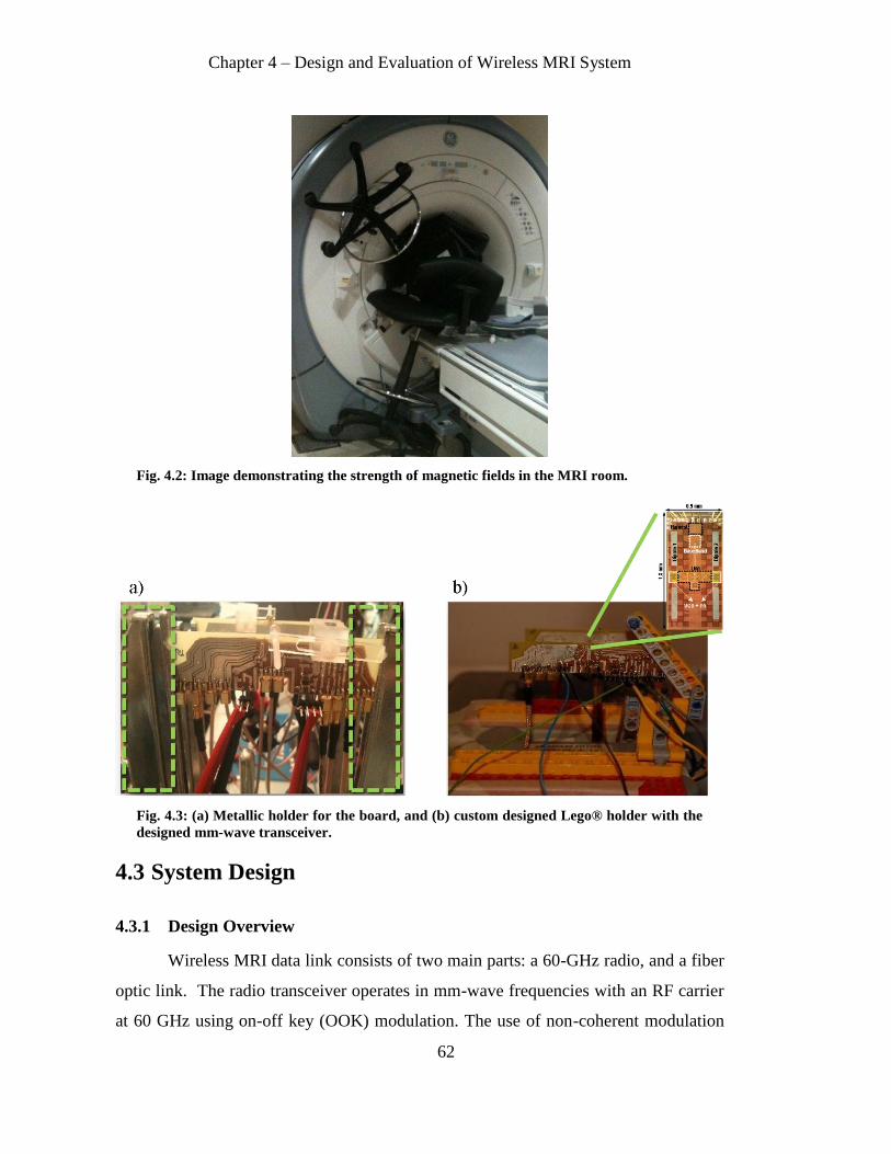
Chapter 4 – Design and Evaluation of Wireless MRI System
62
Fig. 4.2: Image demonstrating the strength of magnetic fields in the MRI room.
Fig. 4.3: (a) Metallic holder for the board, and (b) custom designed Lego® holder with the
designed mm-wave transceiver.
4.3 System Design
4.3.1 Design Overview
Wireless MRI data link consists of two main parts: a 60-GHz radio, and a fiber
optic link. The radio transceiver operates in mm-wave frequencies with an RF carrier
at 60 GHz using on-off key (OOK) modulation. The use of non-coherent modulation

Chapter 4 – Design and Evaluation of Wireless MRI System
63
like OOK simplifies the system architecture as the TX and RX are not required to be
phase synchronized. As the absolute phase of the system is not a concern, it relaxes the
linearity constraints for the power amplifier (PA) design, thus allowing the use of a
more efficient non-linear PA. This reduces system power consumption allowing
operation with small non-magnetic batteries. An earlier version of this transceiver was
used for short range, high data-rate, near field communication (NFC) system [11] and
was discussed in detail in chapter 3. The TX power of the new design scales from 1.3
mW to 14.0 mW as the data rate is varied from 200 Mb/s to 2500 Mb/s, while the RX
consumes a fixed DC power of 76 mW and works up to 2500 Mb/s. The 60-GHz radio
occupies a die area of 0.9 × 1.8 mm2 (1.62 mm2) and was designed and fabricated
using a TSMC 40-nm 9-metal CMOS GP process.
4.3.2 60-GHz Radio
The 60-GHz radio IC is comprised of a TX and an RX block. An on-chip
dipole antenna is shared between the TX and RX blocks via a transmit-receive (TR)
switch. The radio architecture along with signal waveforms at different points inside
the TX and RX blocks is shown in Fig. 4.4. Significant changes were made from the
prior design [11] to target MRI systems. As most of the commercially available analog
to digital convertors (ADCs) for MRI provide a low voltage differential signaling
(LVDS) output, an LVDS receiver was added to the radio baseband. Further, the
baseband was modified to provide support for both return-to-zero (RZ) and non-
return-to-zero (NRZ) signaling protocols. The previous version only supported RZ.
This was done as the ADCs output is normally in NRZ format. Additional circuitry
was added to enable clock and data synchronization between multiple transmitters.
This allows multiple transmitters to be operated at the same time without interference,
using built-in time division multiplexing (TDM) logic. Changes were also made to the
power management circuit to minimize the leakage power. On the RF side, a dedicated
TX was designed without the TR switch thus leading to a higher drain efficiency for
the PA. For the benefit of the readers a brief overview of different circuit blocks is
provided here. For a detailed circuit analysis of different blocks the readers are
advised to refer to chapter 3.

Chapter 4 – Design and Evaluation of Wireless MRI System
64
4.3.2.1 Transmitter Block
The transmitter consists of a digital baseband followed by an RF front end. The
digital data is fed to the transmitter baseband circuitry which supports both NRZ and
RZ signaling protocols. The width of the RZ pulse can be programmed to assume any
value from 250 ps to 1200 ps using a 6-bit pulse width controller (PWC). This RZ
pulse is then fed to the transmitter radio RF front-end. The RF front-end consists of
two identical TX elements each consisting of a voltage controlled oscillator (VCO), a
power amplifier (PA), and an on-chip dipole antenna. To improve the on-chip antenna
gain, the fabricated die was thinned down to 100 µm to minimize substrate losses and
surface waves. The thinned die is mounted on a 600 µm thick FR4 printed circuit
board (PCB) for measurements.
The VCO is a cross-coupled NMOS LC-oscillator and drives a class E/F2, odd
PA with a simulated drain efficiency of 29%. The two VCOs and PAs are switched on
and off, simultaneously, by the PWC modified RZ bit stream to generate impulse radio
ultra-wide-band (IR-UWB) waveforms at the two dipole antennas.
Fig. 4.4: (a) mm-wave radio architecture, and (b) signal waveforms at different points
inside the TX and RX.
4.3.2.2 Receiver Block
The receiver consist of an RF front end followed by a digital baseband. The RF
front end consists of an on-chip dipole antenna followed by a 3-stage transformer-
coupled low noise amplifier (LNA). The LNA is an NMOS common source amplifier.
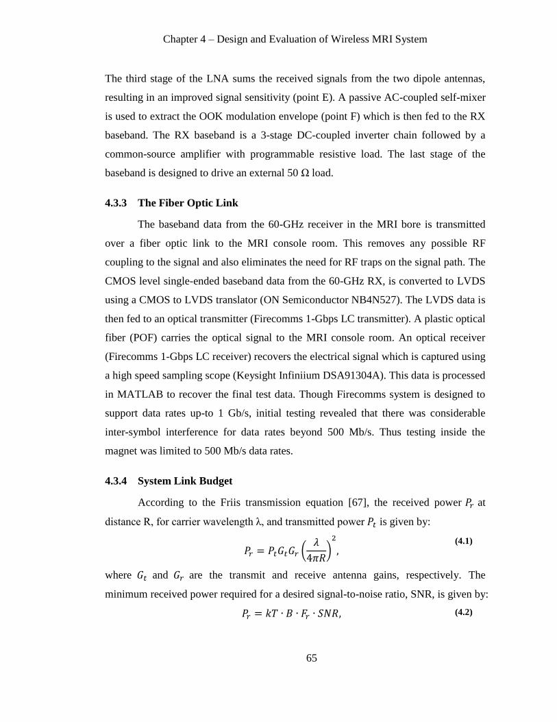
Chapter 4 – Design and Evaluation of Wireless MRI System
65
The third stage of the LNA sums the received signals from the two dipole antennas,
resulting in an improved signal sensitivity (point E). A passive AC-coupled self-mixer
is used to extract the OOK modulation envelope (point F) which is then fed to the RX
baseband. The RX baseband is a 3-stage DC-coupled inverter chain followed by a
common-source amplifier with programmable resistive load. The last stage of the
baseband is designed to drive an external 50 Ω load.
4.3.3 The Fiber Optic Link
The baseband data from the 60-GHz receiver in the MRI bore is transmitted
over a fiber optic link to the MRI console room. This removes any possible RF
coupling to the signal and also eliminates the need for RF traps on the signal path. The
CMOS level single-ended baseband data from the 60-GHz RX, is converted to LVDS
using a CMOS to LVDS translator (ON Semiconductor NB4N527). The LVDS data is
then fed to an optical transmitter (Firecomms 1-Gbps LC transmitter). A plastic optical
fiber (POF) carries the optical signal to the MRI console room. An optical receiver
(Firecomms 1-Gbps LC receiver) recovers the electrical signal which is captured using
a high speed sampling scope (Keysight Infiniium DSA91304A). This data is processed
in MATLAB to recover the final test data. Though Firecomms system is designed to
support data rates up-to 1 Gb/s, initial testing revealed that there was considerable
inter-symbol interference for data rates beyond 500 Mb/s. Thus testing inside the
magnet was limited to 500 Mb/s data rates.
4.3.4 System Link Budget
According to the Friis transmission equation [67], the received power 𝑃𝑟 at
distance R, for carrier wavelength λ, and transmitted power 𝑃𝑡 is given by:
𝑃𝑟 = 𝑃𝑡𝐺𝑡𝐺𝑟 (
𝜆
4𝜋𝑅)
2
, (4.1)
where 𝐺𝑡 and 𝐺𝑟 are the transmit and receive antenna gains, respectively. The
minimum received power required for a desired signal-to-noise ratio, SNR, is given by:
𝑃𝑟 = 𝑘𝑇 ∙ 𝐵 ∙ 𝐹𝑟 ∙ 𝑆𝑁𝑅, (4.2)
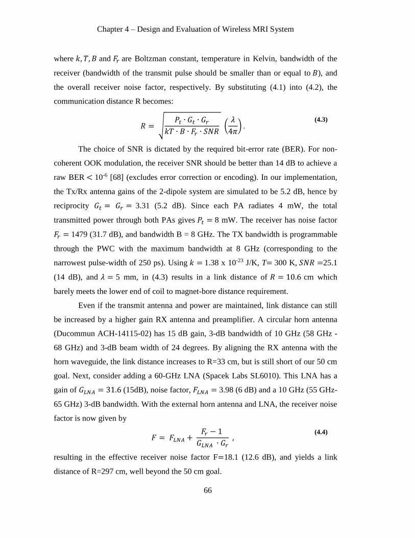
Chapter 4 – Design and Evaluation of Wireless MRI System
66
where 𝑘, 𝑇, 𝐵 and 𝐹𝑟 are Boltzman constant, temperature in Kelvin, bandwidth of the
receiver (bandwidth of the transmit pulse should be smaller than or equal to 𝐵), and
the overall receiver noise factor, respectively. By substituting (4.1) into (4.2), the
communication distance R becomes:
𝑅 = √𝑃𝑡 ∙ 𝐺𝑡 ∙ 𝐺𝑟
𝑘𝑇 ∙ 𝐵 ∙ 𝐹𝑟 ∙ 𝑆𝑁𝑅 (
𝜆
4𝜋) .
(4.3)
The choice of SNR is dictated by the required bit-error rate (BER). For non-
coherent OOK modulation, the receiver SNR should be better than 14 dB to achieve a
raw BER < 10-6 [68] (excludes error correction or encoding). In our implementation,
the Tx/Rx antenna gains of the 2-dipole system are simulated to be 5.2 dB, hence by
reciprocity 𝐺𝑡 = 𝐺𝑟 = 3.31 (5.2 dB). Since each PA radiates 4 mW, the total
transmitted power through both PAs gives 𝑃𝑡 = 8 mW. The receiver has noise factor
𝐹𝑟 = 1479 (31.7 dB), and bandwidth B = 8 GHz. The TX bandwidth is programmable
through the PWC with the maximum bandwidth at 8 GHz (corresponding to the
narrowest pulse-width of 250 ps). Using 𝑘 = 1.38 x 10⁻²³ J/K, T= 300 K, 𝑆𝑁𝑅 =25.1
(14 dB), and 𝜆 = 5 mm, in (4.3) results in a link distance of 𝑅 = 10.6 cm which
barely meets the lower end of coil to magnet-bore distance requirement.
Even if the transmit antenna and power are maintained, link distance can still
be increased by a higher gain RX antenna and preamplifier. A circular horn antenna
(Ducommun ACH-14115-02) has 15 dB gain, 3-dB bandwidth of 10 GHz (58 GHz -
68 GHz) and 3-dB beam width of 24 degrees. By aligning the RX antenna with the
horn waveguide, the link distance increases to R=33 cm, but is still short of our 50 cm
goal. Next, consider adding a 60-GHz LNA (Spacek Labs SL6010). This LNA has a
gain of 𝐺𝐿𝑁𝐴 = 31.6 (15dB), noise factor, 𝐹𝐿𝑁𝐴 = 3.98 (6 dB) and a 10 GHz (55 GHz-
65 GHz) 3-dB bandwidth. With the external horn antenna and LNA, the receiver noise
factor is now given by
𝐹 = 𝐹𝐿𝑁𝐴 +
𝐹𝑟 − 1
𝐺𝐿𝑁𝐴 ∙ 𝐺𝑟 ,
(4.4)
resulting in the effective receiver noise factor F=18.1 (12.6 dB), and yields a link
distance of R=297 cm, well beyond the 50 cm goal.
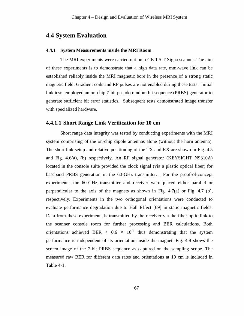
Chapter 4 – Design and Evaluation of Wireless MRI System
67
4.4 System Evaluation
4.4.1 System Measurements inside the MRI Room
The MRI experiments were carried out on a GE 1.5 T Signa scanner. The aim
of these experiments is to demonstrate that a high data rate, mm-wave link can be
established reliably inside the MRI magnetic bore in the presence of a strong static
magnetic field. Gradient coils and RF pulses are not enabled during these tests. Initial
link tests employed an on-chip 7-bit pseudo random bit sequence (PRBS) generator to
generate sufficient bit error statistics. Subsequent tests demonstrated image transfer
with specialized hardware.
4.4.1.1 Short Range Link Verification for 10 cm
Short range data integrity was tested by conducting experiments with the MRI
system comprising of the on-chip dipole antennas alone (without the horn antenna).
The short link setup and relative positioning of the TX and RX are shown in Fig. 4.5
and Fig. 4.6(a), (b) respectively. An RF signal generator (KEYSIGHT N9310A)
located in the console suite provided the clock signal (via a plastic optical fiber) for
baseband PRBS generation in the 60-GHz transmitter. . For the proof-of-concept
experiments, the 60-GHz transmitter and receiver were placed either parallel or
perpendicular to the axis of the magnets as shown in Fig. 4.7(a) or Fig. 4.7 (b),
respectively. Experiments in the two orthogonal orientations were conducted to
evaluate performance degradation due to Hall Effect [69] in static magnetic fields.
Data from these experiments is transmitted by the receiver via the fiber optic link to
the scanner console room for further processing and BER calculations. Both
orientations achieved BER < 0.6 × 10⁻⁶ thus demonstrating that the system
performance is independent of its orientation inside the magnet. Fig. 4.8 shows the
screen image of the 7-bit PRBS sequence as captured on the sampling scope. The
measured raw BER for different data rates and orientations at 10 cm is included in
Table 4-1.
Chapter 4 – Design and Evaluation of Wireless MRI System
68
Fig. 4.5: A block diagram showing the test setup for link verification inside the MRI room
at a distance of 10 cm.
Fig. 4.6: (a) The test setup showing TX and RX alignment, and (b) a magnified view of
PCB mounting showing the 60-GHz TX and the 60-GHz RX chip.
Fig. 4.7: MRI test setup placed (a) in-line with the direction of the static magnetic field, and
(b) perpendicular to the direction of the static magnetic field.

Chapter 4 – Design and Evaluation of Wireless MRI System
69
Fig. 4.8: Differential 7-bit PRBS sequence as captured on the sampling scope at 500 Mb/s
for a distance of 10 cm (voltage scale: 200 mV/div, time scale: 50 ns/div).

4.4.1.2 Link Verification at 25 cm, 50 cm and 65 cm
For link distances greater than 10 cm, additional gain elements were added to
the receiver chain as discussed in section 4.3.4. A horn antenna placed before the 60-
GHz radio receiver improved the link distance to 25 cm. However, the measured worst
case BER of 9.25 × 10⁻⁵ is higher than the expected BER of 10-6. We speculate that
this is due to the misalignment between the horn antenna, TX and RX. Furthermore,
the transmitter center frequency of 56.5 GHz falls outside the antenna 3-dB gain
bandwidth. This reduces antenna gain and increases receiver noise figure, and
therefore adversely impacts the BER.
Fig. 4.9: A block diagram showing the test setup for link verification inside the MRI room
at a distance of 25 cm.
Fig. 4.10: The test setup showing the TX and RX alignment at 25 cm.

Chapter 4 – Design and Evaluation of Wireless MRI System
71
Fig. 4.11: (a) Magnified view of RX aligned to the output of the horn antenna. (b) The test
setup for 25 cm link placed inside the MRI bore.
The block diagram of the setup is shown in Fig. 4.9. The TX, RX and Horn
assembly were mounted on a custom designed slider made of MRI safe materials (Fig.
4.10). The slider allowed for a variable distance between the TX and RX without
disturbing the system component alignment. Only axial orientations were tested due to
space restrictions (Fig. 4.11). We note that there was no detectable performance
degradation due to Hall Effect in the short range experiments. We assume that this
holds for long range experiments as well.
Fig. 4.12: A block diagram showing the test setup for link verification inside the MRI room
at a distance of 50 cm, and 65 cm.
The TX-RX distance was further increased to 50 cm and then to 65 cm by
adding an external LNA to the horn antenna output as shown in Fig. 4.12, Fig. 4.13,

Chapter 4 – Design and Evaluation of Wireless MRI System
72
and Fig. 4.14. The measured BER for different date rates and link distances is
summarized in Table 4-1. The sampling scope used for capturing the BER had a
limited memory depth resulting in one million data points. Even after multiple data
captures, no error was observed for any chunk of one million points suggesting that
the BER is <1.0 × 10⁻⁶.
Fig. 4.13: The test setup showing the TX and RX alignment at 50 cm and 65 cm.
Fig. 4.14: (a) Magnified view of RX aligned to the output of the LNA-horn antenna
assembly. (b) The test setup for 50 cm and 65 cm link placed inside the MRI bore.

Chapter 4 – Design and Evaluation of Wireless MRI System
73
Table 4-1: BER for Different Distance and Data Rates
TX-RX
Distance
BER
@200 Mb/s
BER
@250 Mb/s
BER
@ 500 Mb/s
10 cm 1x10⁻⁶ 1x10⁻⁶ 6.4x10⁻⁶
10 cm* 1x10-6 1x10⁻⁶ 4.8x10⁻⁶
25 cm 3.2x10⁻⁵ 3.9x10⁻⁵ 9.2x10⁻⁵
50 cm 1x10⁻⁶ 1x10⁻⁶ 1x10⁻⁶
65 cm 1x10⁻⁶ 1x10⁻⁶ 1x10⁻⁶
* Setup was placed perpendicular to the external magnetic field as shown in Fig. 4.7(b). All other
measurements were taken by placing the setup along the external static magnetic field.
4.4.1.3 Image Transfer over 50 cm
Having established link reliability, synthesized MRI image transmission was
attempted over a link distance of 50 cm. The PRBS function was replaced by a base-
band processing unit implemented in a FPGA board (Xilinx Kintex-7 FPGA KC705),
and the data recovery processing was implemented in MATLAB. The baseband
architectural details are highlighted in Fig. 4.15. A previously acquired 256 × 256
MRI image was reformatted to 9 sub-blocks of fixed precision 16-bit real and
imaginary pixels. The image blocks were serialized to a bit sequence, and converted to
the RZ format. Lastly, run length limited (RLL) coding was applied. The RLL
operations prevent a DC offset build-up in the analog RF receiver circuitry which
could corrupt the data.
After the image encoding, the encoded bit streams were downloaded to the
FPGA board memory. Upon external triggering, the binary data was transferred at
200MHz over POF to the mm-wave link inside the magnet, where it was envelope
detected in the 60-GHz receiver at 50 cm separation, returned over a second POF link
to the console room, and captured by a high speed sampling oscilloscope (Infinium
DSA91304A).
In MATLAB post-processing of the scope data, clock information was
recovered from the oversampled digital samples, allowing correct bit alignment, and

Chapter 4 – Design and Evaluation of Wireless MRI System
74
subsequent RLL decoding of the bit stream and reformatting into image blocks. The
segmented MRI image and the reconstructed image are shown in Fig. 4.16. The
received image is an exact replica of the original image and no pixel errors were
observed.
(a)
(b)
Fig. 4.15: (a) The baseband processing unit implemented on the transmitter side, and (b)
the baseband processing unit implemented on the receiver side for image processing.
Fig. 4.16: (a) The MRI image broken down into 9 image blocks before transmitting
through the system. (b) The received image obtained by assembling the individually
transmitted blocks. .

Chapter 4 – Design and Evaluation of Wireless MRI System
75
4.4.2 System Measurements outside the MRI Room
The 60-GHz radio can achieve much higher data rates, but was limited in-bore
by the fiber optic channel limit of 500 Mb/s. To assess the true limits, the 60-GHz link
was deployed outside the MRI, and the fiber optic cables were replaced by low loss
SMA cables (Samtec RF316-01SP1-01SP1-0607) and high bandwidth baluns (ETS
PI-102). Under these optimized signal transmission conditions, data rates up to 2.5
Gbps were analyzed, and time domain multiplexing was assessed. These experiments
suggest that the 60-GHz link we have designed is capable of data transfer rates of up
to 2.5 Gbps.
4.4.2.1 Link Verification at 10 cm, 25 cm, 50 cm and 65 cm
BER tests were first repeated for 10-65 cm link distances using identical
methods to those discussed in sections 4.4.1.1 - 4.4.1.2 with on-chip PRBS. The BER
versus data rate for different distances is shown in Fig. 4.17. The measured BER is
identical to that measured inside the MRI bore at the lower data rates. For all
distances, BER increases as the data rate is increased. This is primarily due to finite
receiver bandwidth and a higher inter-symbol interference at higher data rates.

Chapter 4 – Design and Evaluation of Wireless MRI System
76
Fig. 4.17: Bit-error rate versus data rate for 10 cm, 25 cm, 50 cm and 65 cm.
4.4.2.2 Field of View of Horn Antenna
As mentioned in section 4.3.4, the horn antenna used for measurement at 50
cm and above has a 3 dB beamwidth of 24 degree. Hence, even if the transmitter is not
aligned to the receiver horn antenna, the system should still meet the BER
requirements. This is important for an MRI system because a perfect alignment
between the transmitter on a patient’s body and the receiver embedded inside the MRI
bore tube may not always be possible. Thus, with a fixed distance of 50 cm from the
receiver, the transmitter was moved sideways as shown in Fig. 4.18 and measured
BER is shown in Fig. 4.19. Beyond a lateral distance of 7.5 cm, a significant
degradation in BER was observed and it went below the required threshold value of
1×10⁻³ even for lower data rates.

Chapter 4 – Design and Evaluation of Wireless MRI System
77
Fig. 4.18: A block diagram showing the test setup verifying horn antenna’s field of view.
Fig. 4.19: Bit-error rate versus data rate as the transmitter is moved sideways with TX-RX
distance of 50 cm.

Chapter 4 – Design and Evaluation of Wireless MRI System
78
4.4.2.3 Stress Test of the Link at 50 cm
Our BER statistical floor was limited to 10-6 by our instrumentation. As
discussed in the section 4.3.4, the available link margin could possibly result in a
much superior BER than the target value of 10-6. Thus BER measurements were
carried out using a bit error rate tester (Tektronix BERTSscope Si 17500C, courtesy
Marvell). The experiments were carried out using NRZ PRBS-7 at 2 Gb/s and 2.5
Gb/s. The real time eye diagram corresponding to a measured BER of 8.25×10⁻¹² at 2
Gb/s for a distance of 50 cm is shown in Fig. 4.20.
Fig. 4.20: (a) Real time eye diagram measured using the BERTScope at 2 Gb/s, and (b) the
measured BER at 2 Gb/s using PRBS-7.
Fig. 4.21: (a) Real time eye diagram measured using the BERTScope at 2.5 Gb/s, and (b)
the measured BER at 2.5 Gb/s using PRBS-7.

Chapter 4 – Design and Evaluation of Wireless MRI System
79
At 2.5 Gb/s, the BER dropped to 2.42×10⁻⁵ as shown in Fig. 4.21. The drastic
degradation in BER after 2 Gb/s matches with the general waterfall curves for BER
v/s energy per bit to noise spectral density 𝐸𝑏/𝑁0 [68]. The 𝐸𝑏/𝑁0 is related to SNR as
𝐸𝑏
𝑁𝑜= 𝑆𝑁𝑅 ∙
𝐵𝑤
𝐹𝑠 ,
(4.5)
where 𝐹𝑠 is the system data rate, 𝐵𝑤 is the channel bandwidth. As the system data rate
goes up, 𝐸𝑏/𝑁0 falls, resulting in a higher BER. As data rates increase, the errors
increases due to inter symbol interference, since more bits are packed closer and sent
through the channel.
4.4.2.4 Time Domain Multiplexing (TDM)
As mentioned in section 4.3.2.1, the TX baseband supports TDM. Data from
multiple transmitters can be received at a single RX without any interference. The test
setup is shown in Fig. 4.22, and Fig. 4.23, where two TXs are placed with a lateral gap
of 5 cm between them such that both are at a distance of 50 cm from the RX.
Fig. 4.22: The block diagram showing the test setup for multiple transmitters at a distance
of 50 cm from the receiver.
Fig. 4.24(a) shows the screen shot of the initial received data for a data rate of
250 Mb/s. There is a significant overlap in the received data resulting in severe data
corruption. Fig. 4.24(b) shows the same data after TDM is enabled in the TX baseband.

Chapter 4 – Design and Evaluation of Wireless MRI System
80
There is no overlap between the data from different TX, thus the data from each TX
can be reliably deciphered at the RX.
Fig. 4.23: The test setup for multiple TX to demonstrate time division multiplexing (TDM)
at a data rate of 250 Mb/s and distance of 50cm.
Fig. 4.24: Different shaped markers showing the received data corresponding to different
transmitters when the (a) TDM block is turned OFF (voltage scale: 100 mV/div, time scale:
1 ns/div), and (b) when the TDM block is turned ON (voltage scale: 100 mV/div, time scale:
2 ns/div).
4.4.3 Power Consumption for Different Signaling Schemes
The 60-GHz radio supports multiple signaling schemes as mentioned in section
4.3.2.1. Fig. 4.25 shows the TX power consumption for different modulation schemes
as the data rate is varied from 200 Mb/s – 2500 Mb/s. The 60-GHz TX consumes DC
power only while transmitting a data bit value of “1” because the TX is off while it is

Chapter 4 – Design and Evaluation of Wireless MRI System
81
transmitting a data value of “0”. Thus, by using the PWC with RZ OOK, the power
consumption of the TX scales with the data rate.
Fig. 4.25: Transmitter dc power consumption versus data rate for different signaling
schemes.
In addition to the data rate, the TX power consumption scales linearly with the
pulse width. As shown in Fig. 4.4(b), the transmitter consumes power only during
pulse width 𝑇 when both the VCO and PA are turned on. It consumes only leakage
power outside the pulse width 𝑇. The average DC power consumption of a single
pulse is
𝑃𝑠_𝑝𝑢𝑙𝑠𝑒 =
𝑇
𝜏𝑃𝑝𝑢𝑙𝑠𝑒 = 𝑇 ∙ 𝑑𝑎𝑡𝑎𝑟𝑎𝑡𝑒 ∙ 𝑃𝑝𝑢𝑙𝑠𝑒 ,
(4
.6)

Chapter 4 – Design and Evaluation of Wireless MRI System
82
where 𝑃𝑝𝑢𝑙𝑠𝑒 is the sum of both VCO and PA power consumptions and is the bit
duration. A pulse width of 400 ps was used for measurements outside the MRI room
resulting in a TX power consumption of 14mW from a 1.1 V supply at 2500 Mb/s.
This corresponds to an energy per bit of 5.6 pJ/bit for the TX. When the PWC is
turned off, the TX power consumption is almost constant for different data rates. The
slight increase in power consumption with data rate is due to an increase in dynamic
power consumption of the digital circuits.
As the receiver is always on, the power consumption is independent of the
modulation type and the data rate. The RX consumes 76.8 mW of power from a 1.3 V
supply.
4.5 Discussion
This work demonstrated that a high data rate, mm-wave link can be established
reliably inside the MRI magnetic bore in the presence of strong static magnetic fields.
Gradients and RF pulses were not enabled because the cabling needed for testing the
wireless MRI system would expose the mm-wave radio to induced voltages if
gradients and RF pulses were present. We note that these cables would not exist whilst
the wireless system is in use. In agreement with this, when a gradient echo (GRE)
sequence was run with all cabling removed, the 60-GHz radio performance remained
unaltered after later reconnection. We also expect that the OOK modulation, which
does not require phase synchronous detection, will be more robust in the presence of
gradient field perturbations, and optionally, data could be timed to transmit only in
MRI RF-silent intervals if RF overload were an issue.
The minimum SNR is dictated by the required bit-error rate (BER). For non-
coherent OOK, the receiver SNR must exceed 14 dB to get a raw BER < 10-6 [68]
(before error correction or encoding). By comparison, the raw BER specification for
802.11n WiFi and Bluetooth are 10-2 and 10-3 respectively [64] - [66]. From our link
analysis, this was achieved with a 15dB link margin at 50 cm using the horn/LNA
additions to the receiver. A 6 dB increase in receive antenna gain or decrease in
receiver noise figure increases the link distance by a factor of 2. The target BER below
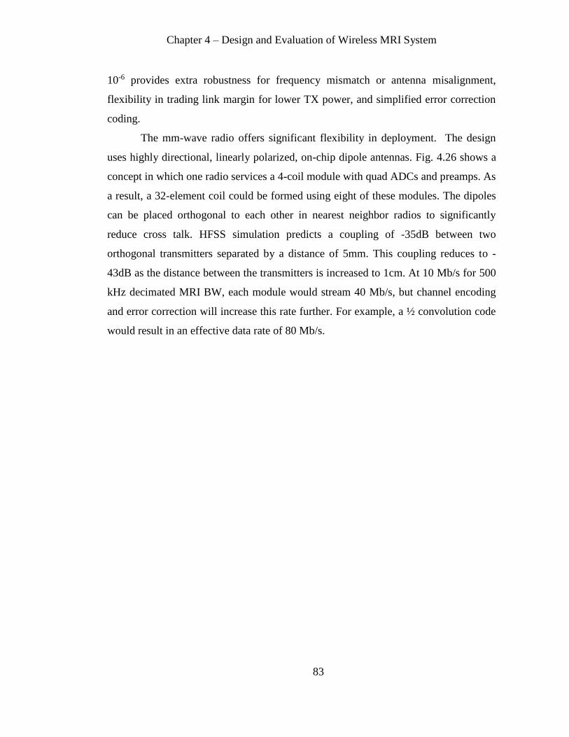
Chapter 4 – Design and Evaluation of Wireless MRI System
83
10-6 provides extra robustness for frequency mismatch or antenna misalignment,
flexibility in trading link margin for lower TX power, and simplified error correction
coding.
The mm-wave radio offers significant flexibility in deployment. The design
uses highly directional, linearly polarized, on-chip dipole antennas. Fig. 4.26 shows a
concept in which one radio services a 4-coil module with quad ADCs and preamps. As
a result, a 32-element coil could be formed using eight of these modules. The dipoles
can be placed orthogonal to each other in nearest neighbor radios to significantly
reduce cross talk. HFSS simulation predicts a coupling of -35dB between two
orthogonal transmitters separated by a distance of 5mm. This coupling reduces to -
43dB as the distance between the transmitters is increased to 1cm. At 10 Mb/s for 500
kHz decimated MRI BW, each module would stream 40 Mb/s, but channel encoding
and error correction will increase this rate further. For example, a ½ convolution code
would result in an effective data rate of 80 Mb/s.
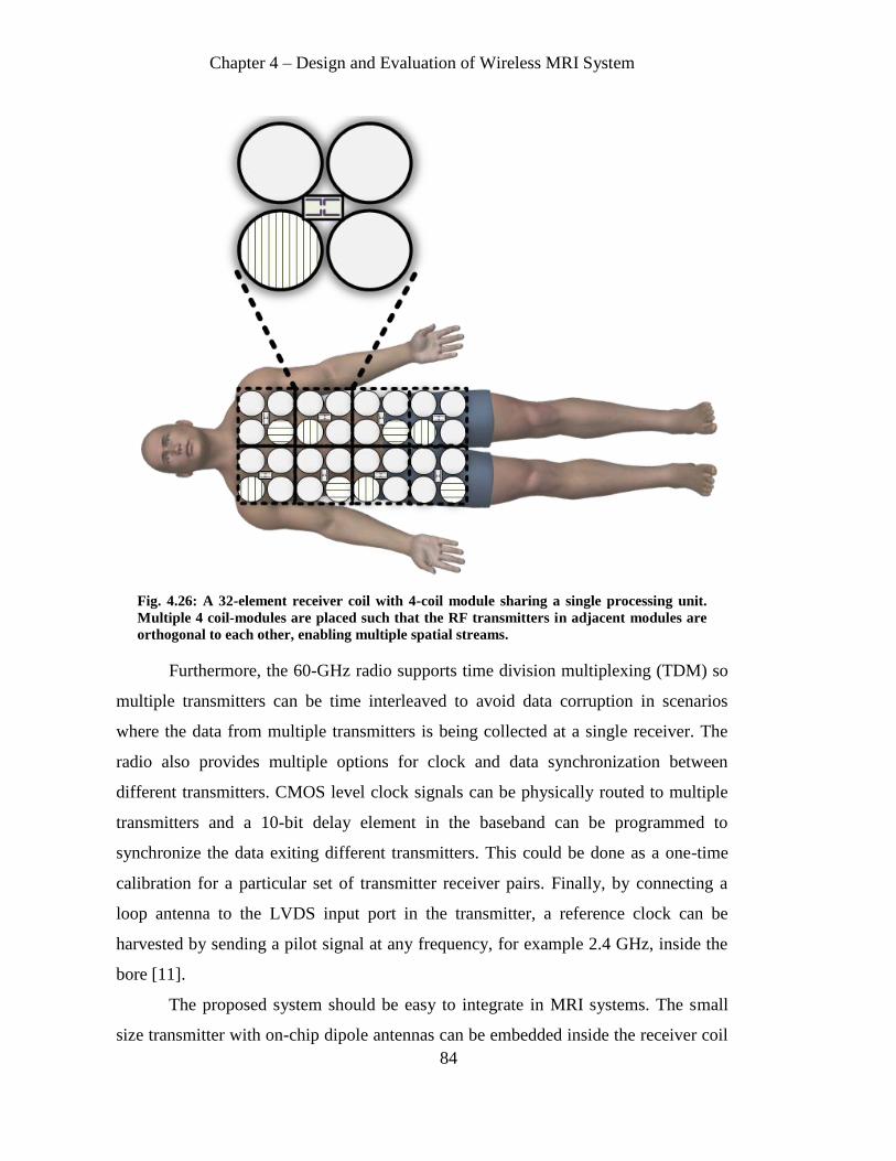
Chapter 4 – Design and Evaluation of Wireless MRI System
84
Fig. 4.26: A 32-element receiver coil with 4-coil module sharing a single processing unit.
Multiple 4 coil-modules are placed such that the RF transmitters in adjacent modules are
orthogonal to each other, enabling multiple spatial streams.
Furthermore, the 60-GHz radio supports time division multiplexing (TDM) so
multiple transmitters can be time interleaved to avoid data corruption in scenarios
where the data from multiple transmitters is being collected at a single receiver. The
radio also provides multiple options for clock and data synchronization between
different transmitters. CMOS level clock signals can be physically routed to multiple
transmitters and a 10-bit delay element in the baseband can be programmed to
synchronize the data exiting different transmitters. This could be done as a one-time
calibration for a particular set of transmitter receiver pairs. Finally, by connecting a
loop antenna to the LVDS input port in the transmitter, a reference clock can be
harvested by sending a pilot signal at any frequency, for example 2.4 GHz, inside the
bore [11].
The proposed system should be easy to integrate in MRI systems. The small
size transmitter with on-chip dipole antennas can be embedded inside the receiver coil

Chapter 4 – Design and Evaluation of Wireless MRI System
85
array without influencing the MRI performance. When the radio chip is encapsulated
in a dielectric lens assembly with a metal reflector as shown in Fig. 4.27 , the radio
antenna gain is simultaneously enhanced to 9.1 dBi [70]. On the receiver side, the
horn-LNA-60-GHz radio assembly can be easily embedded inside the bore magnet,
but similar gains and steerable sensitivity are ultimately best achieved by a beam
steering 60-GHz receive array. Finally as the signal from the magnet to the console
can be transferred over the fiber optic link, it will not couple and corrupt any existing
RF signal in the magnet.
Fig. 4.27: (a) 60-GHz radio with on-chip dipole placed inside an MRI safe package, and (b)
its HFSS simulated radiation pattern with maximum gain of 9.1dBi. The metal acts as a
reflector and the dielectric as a lens for enhanced gain.

Chapter 5 – Conclusions
86
CHAPTER 5
Conclusions
5.1 Conclusions
We have proposed a 60-GHz short-range radio system that offers a low power
and scalable solution for wireless MRI digital links. As compared to analog
transmission, digital transmission offers better noise immunity, stability and flexibility.
The 60-GHz radio supports high data rates generated by commercially available ADCs
designed to meet MRI dynamic range and SNR requirements. The use of fiber optic
link to transport the data beyond the magnet to the console for image reconstruction
minimizes any possible data corruption from existing MRI signals. Fig. 5.1 illustrates
a potential implementation of the proposed wireless MRI system with wireless
receiver coil placed on the patient’s body and its associated wireless receiver with
fiber optic connections embedded inside the MRI bore tube.
Fig. 5.1: Proposed implementation for the designed wireless MRI system.

Chapter 5 – Conclusions
87
5.2 Future Work
The 60-GHz radio is just a first step towards the development of a wireless
MRI system. Significant effort is needed for low power digitizing and decimation of
the MRI coil data before transmission. A conventional MRI receiver chain of preamp,
quad pipeline ADC and serializer (e.g. TI-TL5500, ADS5263, DS32EL0421) alone
results in a DC power budget of 600mW/element, and could easily reach 1W/channel
once other control electronics are added. If a receive chain <100mW/channel were
realizable by passive mixer down-conversion and SAR or continuous time sigma delta
ADCs, one could envision a 32-128 channel wearable array supplied by non-magnetic
battery or even wireless power delivery [71].
In present systems, the above 100 MS/s pipeline ADC sample rate results in
raw data of 1.6 Gb/s for a single array element – a rate that would overwhelm the
802.11ac standard. By locally decimating to 500 KS/s (a high speed MRI case), 20 bit
I/Q and 50% Rx duty cycle, a much more reasonable data rate of 10 Mb/s per element
is achieved. Thus the required data throughput for a receiver array would vary from
320 Mb/s to 1280 Mb/s for 32 to 128 elements. These rates are borderline feasible for
single-stream 802.11ac (5 GHz) but achievable in the 60 GHz 802.11ad standard and
by our technology. An open question is whether the WiFi standards, which employ
phase-coherent modulations, are robust to MRI RF bursts, potential gradient
waveform perturbations of VCOs, and whether they can co-ordinate data streaming
with the MRI pulse sequences.
Although it has been over 2 decades since wireless MRI coils were first
proposed, our on-chip MRI system is a first-of-a-kind demonstration that proves
beyond doubt that wireless MRI is very much feasible. However, widespread adoption
of wireless MRI would be possible only if the subsystems such as pre-amps,
ADCs and serializer become more power efficient than today. We believe that our
experimental demonstration of wireless MRI will encourage future research in
improving the power efficiency of these subsystems and thereby contribute to the
development of wireless MRI systems.

88

Bibliography
[1] [Online]. Available: http://www.magnetic-resonance.org.
[2] [Online]. Available: http://radiopaedia.org/.
[3] [Online]. Available: http://mri-q.com/.
[4] [Online]. Available: https://www.maximintegrated.com/en/app-
notes/index.mvp/id/4681.
[5] Y. Murakami, T. Tetsuhiko and Y. Etsuji, "Nuclear magnetic resonanace
inspection apparatus and its method.". US Patent 5,384,536, 24 Jan 1995.
[6] E. Boskamp et al., "Wireless RF Module for an MR imaging system.". US Patent
2003/020619A1, Nov 2003.
[7] G. Scott and K. Yu, "Wireless transponders for RF coils: systems issues," in
Proceedings of the 13th Annual Meeting of ISMRM, Miami, Florida, USA,
2005.
[8] M. J. Riffe et al., "Using on-board microprocessors to control a wireless MR
receiver array," in Proceedings of the 17th Annual Meeting of ISMRM,
Honolulu, Hawaii, USA, 2009.
[9] J. Wei et al., "A realization of digital wireless transmission for MRI signals based
on 802.11 b," Journal of Magnetic Resonance , vol. 186, no. 2, pp. 358-
363, 2007.
[10] O. Heid et al., "CUTTING THE CORD-WIRELESS COILS FOR MRI," in Proc.
Intl. Soc. Mag. Reson. Med, 2009.
[11] M. Taghivand, K. Aggarwal, Y. Rajavi and A. S. Y. Poon, "An Energy
Harvesting 2 × 2 60 GHz Transceiver With Scalable Data Rate of 38–2450
Mb/s for Near-Range Communication," IEEE Journal of Solid-State
Circuits, vol. 50, no. 8, pp. 1889-1902, Aug. 2015.
[12] TEXAS INSTRUMENTS, "Quad Channel 16-Bit, 100MSPS High-SNR ADC,"
ADS5263 datasheet, May. 2011-Rev. Jan. 2013.
[13] TEXAS INSTRUMENTS, "DS32EL0421, DS32ELX0421 125 - 312.5 MHz
FPGA-Link Serializer with DDR LVDS Parallel Interface," DS32EL0421
datasheet, May. 2008-Rev. Apr. 2013.
[14] [Online]. Available:
http://www.cisco.com/c/en/us/products/collateral/wireless/aironet-3600-
series/white_paper_c11-713103.html.
[15] Aruba Networks, "802.11AC IN-DEPTH," Sunnyvale, 2014.
[16] [Online]. Available: http://www.dell.com/Support/Article/us/en/19/QNA43752.
[17] Y. Zeng et al., "A first look at 802.11ac in action: Energy efficiency and
interference characterization," in 2014 IFIP Networking Conference, 2-4
Bibliography
90
June 2014.
[18] S. Joshi et al., "Effect of antenna spacing on the performance of multiple input
multiple output LTE downlink in an urban microcell," International
Journal of Wireless & Mobile Networks, vol. 4, no. 6, pp. 175 - 188, Dec.
2012.
[19] S. K. Saha et al., "Power-throughput tradeoffs of 802.11n/ac in smartphones," in
IEEE Conference on Computer Communications (INFOCOM), 2015, April
26 2015-May 1 2015.
[20] [Online]. Available: http://www.radio-electronics.com/info/wireless/wi-fi/ieee-
802-11ad-microwave.php.
[21] Agilent Technologies, "Wireless LAN at 60 GHz - IEEE 802.11ad Explained,"
Agilent Technologies, May 2013.
[22] [Online]. Available: http://www.sibeam.com/.
[23] [Online]. Available: http://wilocity.com/.
[24] [Online]. Available: http://www.tensorcom.com/.
[25] M. Boers et al., "A 16 TX/16 RX 60 GHz 802.11ad chipset with single coaxial
interface and polarization diversity," in IEEE ISSCC Dig. Tech. Papers,
Feb. 2014.
[26] T. Tsukizawa et al., "A fully integrated 60 GHz CMOS transceiver chipset based
on WiGig/IEEE802.11ad with built-in self calibration for mobile
applications," in IEEE ISSCC Dig. Tech. Papers, Feb. 2013.
[27] J. Lee et al., "A low-power fully integrated 60 GHz transceiver system with OOK
modulation and on-board antenna assembly," in IEEE ISSCC Dig. Tech.
Papers, Feb. 2009.
[28] K. Okada et al., "A full 4-Channel 6.3 Gb/s 60 GHz direct-conversion transceiver
with low-power analog and digital baseband circuitry," in IEEE ISSCC
Dig. Tech. Papers, Feb. 2012.
[29] T. Mitomo et al., "A 2 Gb/s-Throughput CMOS transceiver chipset with
inpackage antenna for 60 GHz short-range wireless communication," in
IEEE ISSCC Dig. Tech. Papers, Feb. 2012.
[30] E. Cohen et al., "A CMOS bidirectional 32-element phased-array transceiver at
60 GHz with LTCC antenna," in IEEE Radio Frequency Integrated
Circuits Symp. (RFIC), Jun. 2012.
[31] J. M. Gilbert et al., "A 4-Gbps uncompressed wireless HD A/V transceiver
chipset," IEEE. Micro, vol. 28, no. 2, pp. 56-64, 2008.
[32] M. Taghivand and A. S. Y. Poon, "Supporting and enabling circuits for antenna
arrays in wireless communications," Proc. IEEE, vol. 100, p. 2207–2218,
2012.
[33] S. Emami et al., "A 60 GHz CMOS phased-array transceiver pair for multi-Gb/s
wireless communications," in IEEE ISSCC Dig. Tech. Papers, Feb. 2011.
[34] A. Balankutty et al., "A 12-element 60 GHz CMOS phased array transmitter on
LTCC package with integrated antennas," in IEEE ASSCC Dig.Tech.

Bibliography
91
Papers, Nov. 2011.
[35] H. Krishnaswamy and H. Hashemi, Integrated Beamforming Arrays in mm-Wave
Silicon Technology: 60 GHz and Beyond, Berlin, Germany: Springer,
2008.
[36] A. Natarajan et al., "A fully-integrated 16-Element phased-array receiver in siGe
BiCMOS for 60-Ghz communications," IEEE J. Solid-State Circuits, vol.
46, no. 5, pp. 1059-1075, May 2011.
[37] K. -J. Koh et al., "A millimeter-wave (40-45 Ghz) 16-Elementvphased-array
transmitter in m SiGe BiCMOS technology," IEEE J. Solid-State Circuits,
vol. 44, no. 5, pp. 1498-1509, May 2009.
[38] A. Valdes-Garcia et al., "A SiGe BiCMOS 16-element phased-array transmitter
for 60 GHz communications," in IEEE ISSCC Dig. Tech. Papers, Feb.
2010.
[39] Y. Yu et al., "A 60 GHz phase shifter integrated with LNA and PA in 65 nm
CMOS for phased array systems," IEEE J. Solid-State Circuits, vol. 45, no.
9, pp. 1697-1709, Sep. 2010.
[40] E. Cohen et al., "A bidirectional TX/RX four-element phased array at 60 GHz
with RF-IF conversion block in 90-nm CMOS process," IEEE Trans.
Microw. Theory Techn., vol. 58, no. 5, pp. 1438-1446, May 2010.
[41] X. Yi et al., "A 57.9-to-68.3 GHz 24.6 mW frequency synthesizer with in-phase
injection-coupled QVCO in 65 nm CMOS," in IEEE ISSCC Dig. Tech.
Papers, Feb. 2013.
[42] L. Kong et al., "A 50 mW-TX 65 mW-RX 60 GHz 4-element phasedarray
transceiver with integrated antennas in 65 nm CMOS," in IEEE ISSCC
Dig. Tech. Papers, Feb. 2013.
[43] A. Siligaris et al., "A low power 60-GHz 2.2-Gbps UWB transceiver with
integrated antennas for short range communications," in Proc.IEEE RFIC
Symp., Jun. 2013.
[44] L. Kong et al., "A mW mm-Wave phased-array transmitter in 65 nm CMOS," in
Proc. Symp. VLSI Circuits, Jun. 2012.
[45] S. D. Kee et al., "The class E/F family of ZVS switching amplifiers," IEEE Trans.
Microw. Theory Techn., vol. 51, no. 6, pp. 1677-1690, Jun. 2003.
[46] A. Valdes-Garcia et al., "A 60 GHz class-E power amplifier in SiGe," in IEEE
ASSCC Dig. Tech. Papers, Nov. 2006.
[47] N. Kalantari et al., "A 19.4 dBm, Q-band class-E power amplifier in a 0.12 um
SiGe BiCMOS process," IEEE MWCL, vol. 20, pp. 283-285, May 2010.
[48] O. T. Ogunnika et al., "A 60 GHz class-E tuned power amplifier with in 32 nm
SOI CMOS," in IEEE Radio Frequency Integrated Circuits Symp. (RFIC),
Jun. 2012.
[49] N. Talwalkar et al., "An integrated 5.2 GHZ CMOS T/R switch with LC-tuned
substrate bias," in IEEE ISSCCDig. Tech. Papers, Feb. 2003.
[50] A. Babakhani et al., "A 77 GHz phased array transceiver with on-chip dipole

Bibliography
92
antennas: receiver and antennas," IEEE J. Solid-State Circuits, vol. 41, no.
12, pp. 2795-2806, Dec. 2006.
[51] M. H. Barakat et al., "On the design of 60 GHz integrated antennas on m SOI
technology," in Proc. of IEEE Int. SOI Conf., 2007.
[52] C. -H. Wang et al., "A 60 GHz transmitter with integrated antenna in m SiGe
BiCMOS technology," in IEEE ISSCC Dig. Tech. Papers, Feb. 2006.
[53] A. Arbabian et al., "A 94 GHz mm-Wave-to-baseband pulsed-radar transceiver
with applications in imaging and gesture recognition," IEEE J. Solid-State
Circuits, vol. 48, no. 4, pp. 1055-1071, Apr. 2013.
[54] N. G. Alexopoulos et al., "Substrate optimization for integrated circuit antennas,"
IEEE Trans. Microw. Theory Techn., vol. 83, p. 550, 1983.
[55] G. M. Rebeiz et al., "Millimeter-wave and terahertz integrated circuit antennas,"
Proc. IEEE, vol. 80, no. 11, pp. 1748-1770, 1992.
[56] D. B. Rutledge et al., "Imaging antenna arrays," IEEE Trans. Antennas Propag.,
vol. 30, pp. 535-540, Jul. 1982.
[57] F. Gutierrez et al., "On-chip integrated antenna structures in CMOS for 60 GHz
WPAN systems," IEEE J. Sel. Areas Commun., vol. 27, no. 8, pp. 1367-
1378, Oct. 2009.
[58] D. P. Neikirk et al., "Far-infrared imaging antenna arrays," Appl. Phys.Lett., pp.
203-205, Feb. 1982.
[59] A. P. Toda et al., "60-GHz substrate materials characterization using the covered
transmission-line method," IEEE Trans. Microw. Theory Techn., vol. 63,
no. 99, pp. 1-13, Mar. 2015.
[60] C. A. Balanis, Antenna Theory Analysis and Design, Third edition, John Wiley &
Sons Inc., 2005.
[61] S. Mandal et al., "Low-power CMOS rectifier design for RFID applications,"
IEEE Trans. Circuits Syst. I, Reg. Papers, vol. 54, no. 6, pp. 1177-1188,
Jun. 2007.
[62] H. Wang et al., "A 60-GHz FSK transceiver with automatically-calibrated
demodulator in 90-nm CMOS," in VLSI Circuits Symp. Dig., Jun. 2010.
[63] J. Lee et al., "A Low-Power Low-Cost Fully-Integrated 60-GHz Transceiver
System with OOK Modulation and On-Board Antenna Assembly," IEEE J
Solid-State Circuits, vol. 45, no. 2, pp. 264-275, Feb. 2010.
[64] F. Peng, J. Zhang and W. E. Ryan, "Adaptive Modulation and Coding for IEEE
802.11n," in IEEE Wireless Communications and Networking Conference,
11-15 March 2007.
[65] A. Goldsmith, Wireless communications, Cambridge university press, 2005.
[66] C. Gehrmann, P. Joakim and B. Smeets, Bluetooth Security (Artech House
Computer Security Series), Colorado: Artech House Publishers, 2004.
[67] H. T. Friis, "A note on a simple transmission formula," in Proc. IRE, 1946.
[68] Q. Tang et al., "BER performance analysis of an on-off keying based minimum

Bibliography
93
energy coding for energy constrained wireless sensor applications," in
IEEE International Conference on Communications, 2005.
[69] E. Hall, "On a New Action of the Magnet on Electric Currents," American
Journal of Mathematics, vol. 2, no. 3, pp. 287-292, 1879.
[70] L. Shafai, "Dielectric Loaded Antennas," in Encyclopedia of RF and Microwave
Engineering, John Wiley & Sons, Apr. 2005.
[71] K. Byron et al., "RF Gated Wireless Power Transfer System," in Proceedings of
the 23rd Annual Meeting of ISMRM, Toronto, Ontario, Canada, 2015.