a transparent diode with high rectifying ratio using...
TRANSCRIPT

A transparent diode with high rectifying ratio using amorphous indium-gallium-zincoxide/SiNx coupled junctionMyung-Jea Choi, Myeong-Ho Kim, and Duck-Kyun Choi Citation: Applied Physics Letters 107, 053501 (2015); doi: 10.1063/1.4927823 View online: http://dx.doi.org/10.1063/1.4927823 View Table of Contents: http://scitation.aip.org/content/aip/journal/apl/107/5?ver=pdfcov Published by the AIP Publishing Articles you may be interested in Reduction of defect formation in amorphous indium-gallium-zinc-oxide thin film transistors by N2O plasmatreatment J. Appl. Phys. 114, 204501 (2013); 10.1063/1.4832327 Investigation of zinc interstitial ions as the origin of anomalous stress-induced hump in amorphous indium galliumzinc oxide thin film transistors Appl. Phys. Lett. 102, 173502 (2013); 10.1063/1.4803536 The impact of SiN x gate insulators on amorphous indium-gallium-zinc oxide thin film transistors under bias-temperature-illumination stress Appl. Phys. Lett. 96, 193506 (2010); 10.1063/1.3429588 The influence of the gate dielectrics on threshold voltage instability in amorphous indium-gallium-zinc oxide thinfilm transistors Appl. Phys. Lett. 95, 123502 (2009); 10.1063/1.3232179 Fabrication of transparent p–n heterojunction thin film diodes based entirely on oxide semiconductors Appl. Phys. Lett. 75, 2851 (1999); 10.1063/1.125171
This article is copyrighted as indicated in the article. Reuse of AIP content is subject to the terms at: http://scitation.aip.org/termsconditions. Downloaded to IP:
166.104.31.108 On: Fri, 07 Aug 2015 02:54:05

A transparent diode with high rectifying ratio using amorphousindium-gallium-zinc oxide/SiNx coupled junction
Myung-Jea Choi, Myeong-Ho Kim, and Duck-Kyun Choia)
Department of Materials Science and Engineering, Hanyang University, Seoul 133-791, South Korea
(Received 20 February 2015; accepted 23 July 2015; published online 3 August 2015)
We introduce a transparent diode that shows both high rectifying ratio and low leakage current at
process temperature below 250 �C. This device is clearly distinguished from all previous transparent
diodes in that the rectifying behavior results from the junction between a semiconductor (amorphous
indium-gallium-zinc oxide (a-IGZO)) and insulator (SiNx). We systematically study the properties of
each junction within the device structure and demonstrate that the a-IGZO/SiNx junction is the
source of the outstanding rectification. The electrical characteristics of this transparent diode are:
2.8 A/cm2 on-current density measured at �7 V; lower than 7.3 � 10�9 A/cm2 off-current density;
2.53 ideality factor; and high rectifying ratio of 108–109. Furthermore, the diode structure has a trans-
mittance of over 80% across the visible light range. The operating principle of the indium-tin oxide
(ITO)/a-IGZO/SiNx/ITO device was examined with an aid of the energy band diagram and we pro-
pose a preliminary model for the rectifying behavior. Finally, we suggest further directions for
research on this transparent diode. VC 2015 AIP Publishing LLC.
[http://dx.doi.org/10.1063/1.4927823]
Transparent electronic devices are becoming increas-
ingly important in various applications. Research has
focused on making standard p-n junction or metal-
semiconductor (MS) diode structures with transparent mate-
rials. Transparent MS diodes use a transparent conductor
such as indium-tin oxide (ITO) in conjunction with a wide-
band gap semiconductor. Since the transparent MS diodes
consisting of transparent conductor such as ITO and wide-
band gap oxide semiconductors did not show strong rectify-
ing behavior due to the similarity in work function between
two materials, more attention has been paid to the p-n junc-
tion based on wide band gap oxide semiconductors.
However, these efforts have suffered from difficulties in
finding a suitable p-type transparent material and the result-
ing oxide semiconductor p-n junction diodes have thus far
been limited by a high leakage current density, which results
in a significantly lower rectifying behavior compared to con-
ventional, non-transparent diodes.1–6
In recent reports, there are p-n junction transparent
diodes having enhanced rectifying ratio as a result of suc-
cessful development in p-type oxide semiconductor.7–9
However, the fabrication of these transparent diodes involves
high process temperatures as high as 600 �C or the pulsed
laser deposition (PLD) method that is not suitable to large
area devices. So, we tried to find other alternative transparent
rectifying junctions that enable low temperature process but
retain high rectifying ratio, low leakage, and good optical
transmittance. The structure of a transparent diode that we
present in Figure 1 consists of a semiconducting amorphous
indium-gallium-zinc oxide (a-IGZO) and an insulating SiNx
layer sandwiched between conducting ITO.
Although the a-IGZO has been studied extensively as an
active layer in thin film transistors, the outstanding rectifying
characteristics of the a-IGZO-insulator junction has not been
reported previously. We systematically study the properties
at each junction within the device and clearly identify the a-
IGZO/SiNx junction as the source of the outstanding rectifi-
cation. We propose a preliminary model for the rectifying
behavior in the ITO/a-IGZO/SiNx/ITO device and suggest
further directions for research on this transparent diode.
This transparent diode was fabricated on soda-lime glass
substrates. A 50 nm thick ITO bottom electrode was first de-
posited by radio frequency (RF) magnetron sputtering. Next,
a 20 nm thick SiNx layer was deposited by plasma enhanced
chemical vapor deposition (PECVD) at 250 �C. The reactant
gases were SiH4 and NH3. Then, the deposition of the a-
IGZO film followed using RF magnetron sputtering from a-
IGZO target (In:Ga:Zn¼ 1:1:1). The ambient atmosphere of
Ar:O2 with a ratio of 9:1 was maintained at 5 mTorr during
the deposition. The RF power was 40 W. A 50 nm thick ITO
FIG. 1. Schematic of the transparent diode structure of ITO/a-IGZO/SiNx/
ITO. Top electrode area has the dimensions of 50 lm � 50 lm.a)Electronic mail: [email protected]
0003-6951/2015/107(5)/053501/4/$30.00 VC 2015 AIP Publishing LLC107, 053501-1
APPLIED PHYSICS LETTERS 107, 053501 (2015)
This article is copyrighted as indicated in the article. Reuse of AIP content is subject to the terms at: http://scitation.aip.org/termsconditions. Downloaded to IP:
166.104.31.108 On: Fri, 07 Aug 2015 02:54:05

layer was deposited as a top electrode. The 50 lm � 50 lm
area of the top electrode was defined by photo lithography
method which was followed by a lift-off process. Finally, the
device was annealed for 1 h at 250 �C in forming gas (H2 5%
and Ar 95%). Separated junctions of ITO/a-IGZO/ITO and
ITO/SiNx/ITO were fabricated with identical deposition and
annealing conditions used for the diode device. The current–
voltage and capacitance-voltage characteristics were measured
using each Agilent E5270B and HP 4284A parameter analyzer.
Optical transmittance was measured using Ultraviolet-visible
spectroscopy (Biochrom Ltd., Cambridge). The transmission
electron microscopy (TEM) was operated with an acceleration
voltage of 300 kV.
Figure 2(a) shows the current density versus voltage
(J-V) characteristics of ITO/a-IGZO/SiNx/ITO structure on a
linear scale. The J-V curve shows strong rectification with an
ideality factor of 2.53, which is similar to previous transpar-
ent oxide diodes. Such a relative high ideality factor is not
uncommon in transparent oxide diode and it is believed to be
associated with an interfacial defect in heterojunction or
deep-level-defect of oxide semiconductor.1–3
In contrast, this diode has a very low leakage current
density in the range of 10–8–10�9 A/cm2, which is shown
more clearly on a logarithmic scale in Figure 2(b). The on-
current density corresponds to 2.8 A/cm2 at �7 V and the
off-state current density is 8.2 � 10�9 A/cm2. This repre-
sents a rectifying ratio in the range of 108�109, which is rel-
atively high compared to the previously reported p-n
junction oxide diode.1–9
In general, rectifying behavior is caused by Schottky
junction formed by difference of work function between
metal and semiconductor or the built-in potential from the
space charge region at p-n junction. It is also caused by the
different work functions between bottom electrode and top
electrode in the Metal-Insulator-Metal (MIM) structure. In
the ITO/a-IGZO/SiNx/ITO structure system, there are three
junctions which may induce the rectifying behavior. We sys-
tematically investigate the J-V characteristics of each of the
three possible junctions independently in order to identify
the junction responsible for the rectifying characteristics in
the ITO/a-IGZO/SiNx/ITO structure.
First, one possible source of rectification is between the
ITO top electrode and the n-type a-IGZO semiconductor. It
is well known that a Schottky barrier formed by the differ-
ence between the metal’s work function and the semiconduc-
tor’s work function can lead to either a rectifying or non-
rectifying junction depending on the barrier height. We
therefore examined the J-V characteristics of an ITO/a-
IGZO/ITO sandwich structure. As shown in Figure 2(c), the
junction shows a clear Ohmic behavior and is highly conduc-
tive. This result is expected since the ITO/a-IGZO combina-
tion is commonly used for its Ohmic behavior in the back
plane transistors of LCDs.
Second, A MIM structure can show rectification under
the condition where there exists a significant difference of
the work function between the top electrode and bottom elec-
trode in order to drive a forward tunneling current.10 To con-
firm that the large rectification ratio does not originate from
the SiNx and ITO bottom electrode junction, the J-V charac-
teristics of the ITO/SiNx/ITO structure are shown in Figure
2(d). The 20 nm thickness of the SiNx layer is the same used
for ITO/a-IGZO/SiNx/ITO device. Although SiNx is an insu-
lator, it permits a tunneling current as the layer becomes
thinner. The tunneling current measured for this junction is
1000 times lower than the on-state current of the full device
structure; therefore, this junction cannot account for the high
rectification ratio. From this experimental evidence, we con-
clude that the rectifying behavior in ITO/a-IGZO/SiNx/ITO
structure is due to the a-IGZO/SiNx junction. Although the
structure of ITO/a-IGZO/SiNx/ITO diode resembles Metal-
Insulator-Semiconductor (MIS) Schottky diode, it is different
from the MIS Schottky diode. In case of MIS Schottky
diode, the rectifying behavior is basically caused by
Schottky contact between metal and semiconductor and the
role of inserted insulating layer is to improve the electrical
properties. For instance, it helps to control the redistribution
of the interface states or reduces the chemical interaction at
the surface.11–13 On the other hand, the SiNx layer is an elec-
trically active and is crucial to cause the rectifying behavior
in this transparent diode. This result is important because
this distinctive rectifying behavior has not been reported pre-
viously. Moreover, we have found such rectifying behavior
when the a-IGZO is coupled with other insulators like SiOx
or Al2O3 (not shown here).
The capacitance versus voltage (C-V) measurement can
elucidate the origin of the low leakage current. The tunneling
current through SiNx by itself was 10�6 A/cm2 (Figure 2(d),
whereas the leakage current of the full device was much
lower at 10�9 A/cm2 (Figure 2(b). This clearly suggests that
a depletion layer within the a-IGZO must contribute strongly
to the resistance of the junction in reverse bias. Figure 3
shows the 1/C2–V plot for the ITO/a-IGZO/SiNx/ITO struc-
ture diode at frequency of 100 kHz. There is a defined linear
region in the range from �2 V to 0.5 V, which confirms the
formation of a depletion mode within the a-IGZO. The ca-
pacitance saturates beyond 1.2 V (reverse bias) suggesting
that the 60 nm a-IGZO layer becomes fully depleted. Taken
FIG. 2. J-V characteristics for the ITO/a-IGZO/SiNx/ITO diode structure in
(a) linear scale and (b) log-scale. J-V characteristics of individual compo-
nent layers: (c) ITO/a-IGZO/ITO and (d) ITO/SiNx/ITO structure.
053501-2 Choi, Kim, and Choi Appl. Phys. Lett. 107, 053501 (2015)
This article is copyrighted as indicated in the article. Reuse of AIP content is subject to the terms at: http://scitation.aip.org/termsconditions. Downloaded to IP:
166.104.31.108 On: Fri, 07 Aug 2015 02:54:05
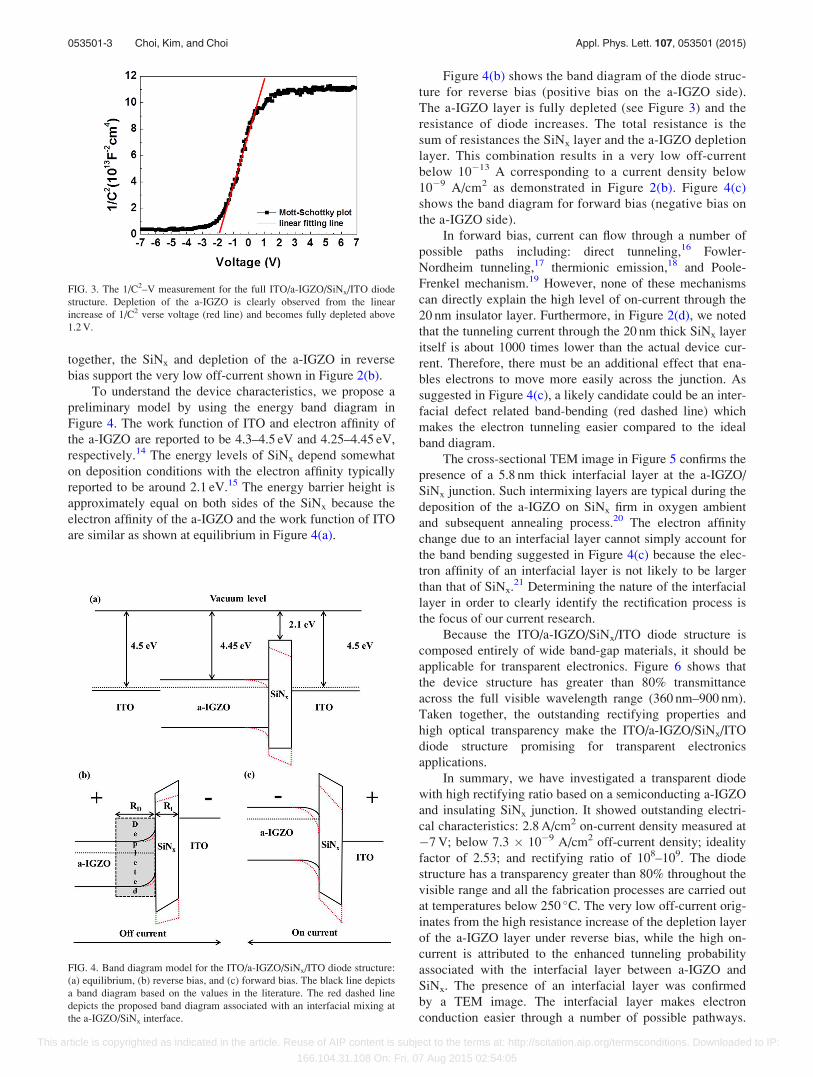
together, the SiNx and depletion of the a-IGZO in reverse
bias support the very low off-current shown in Figure 2(b).
To understand the device characteristics, we propose a
preliminary model by using the energy band diagram in
Figure 4. The work function of ITO and electron affinity of
the a-IGZO are reported to be 4.3–4.5 eV and 4.25–4.45 eV,
respectively.14 The energy levels of SiNx depend somewhat
on deposition conditions with the electron affinity typically
reported to be around 2.1 eV.15 The energy barrier height is
approximately equal on both sides of the SiNx because the
electron affinity of the a-IGZO and the work function of ITO
are similar as shown at equilibrium in Figure 4(a).
Figure 4(b) shows the band diagram of the diode struc-
ture for reverse bias (positive bias on the a-IGZO side).
The a-IGZO layer is fully depleted (see Figure 3) and the
resistance of diode increases. The total resistance is the
sum of resistances the SiNx layer and the a-IGZO depletion
layer. This combination results in a very low off-current
below 10�13 A corresponding to a current density below
10�9 A/cm2 as demonstrated in Figure 2(b). Figure 4(c)
shows the band diagram for forward bias (negative bias on
the a-IGZO side).
In forward bias, current can flow through a number of
possible paths including: direct tunneling,16 Fowler-
Nordheim tunneling,17 thermionic emission,18 and Poole-
Frenkel mechanism.19 However, none of these mechanisms
can directly explain the high level of on-current through the
20 nm insulator layer. Furthermore, in Figure 2(d), we noted
that the tunneling current through the 20 nm thick SiNx layer
itself is about 1000 times lower than the actual device cur-
rent. Therefore, there must be an additional effect that ena-
bles electrons to move more easily across the junction. As
suggested in Figure 4(c), a likely candidate could be an inter-
facial defect related band-bending (red dashed line) which
makes the electron tunneling easier compared to the ideal
band diagram.
The cross-sectional TEM image in Figure 5 confirms the
presence of a 5.8 nm thick interfacial layer at the a-IGZO/
SiNx junction. Such intermixing layers are typical during the
deposition of the a-IGZO on SiNx firm in oxygen ambient
and subsequent annealing process.20 The electron affinity
change due to an interfacial layer cannot simply account for
the band bending suggested in Figure 4(c) because the elec-
tron affinity of an interfacial layer is not likely to be larger
than that of SiNx.21 Determining the nature of the interfacial
layer in order to clearly identify the rectification process is
the focus of our current research.
Because the ITO/a-IGZO/SiNx/ITO diode structure is
composed entirely of wide band-gap materials, it should be
applicable for transparent electronics. Figure 6 shows that
the device structure has greater than 80% transmittance
across the full visible wavelength range (360 nm–900 nm).
Taken together, the outstanding rectifying properties and
high optical transparency make the ITO/a-IGZO/SiNx/ITO
diode structure promising for transparent electronics
applications.
In summary, we have investigated a transparent diode
with high rectifying ratio based on a semiconducting a-IGZO
and insulating SiNx junction. It showed outstanding electri-
cal characteristics: 2.8 A/cm2 on-current density measured at
�7 V; below 7.3 � 10�9 A/cm2 off-current density; ideality
factor of 2.53; and rectifying ratio of 108–109. The diode
structure has a transparency greater than 80% throughout the
visible range and all the fabrication processes are carried out
at temperatures below 250 �C. The very low off-current orig-
inates from the high resistance increase of the depletion layer
of the a-IGZO layer under reverse bias, while the high on-
current is attributed to the enhanced tunneling probability
associated with the interfacial layer between a-IGZO and
SiNx. The presence of an interfacial layer was confirmed
by a TEM image. The interfacial layer makes electron
conduction easier through a number of possible pathways.
FIG. 4. Band diagram model for the ITO/a-IGZO/SiNx/ITO diode structure:
(a) equilibrium, (b) reverse bias, and (c) forward bias. The black line depicts
a band diagram based on the values in the literature. The red dashed line
depicts the proposed band diagram associated with an interfacial mixing at
the a-IGZO/SiNx interface.
FIG. 3. The 1/C2–V measurement for the full ITO/a-IGZO/SiNx/ITO diode
structure. Depletion of the a-IGZO is clearly observed from the linear
increase of 1/C2 verse voltage (red line) and becomes fully depleted above
1.2 V.
053501-3 Choi, Kim, and Choi Appl. Phys. Lett. 107, 053501 (2015)
This article is copyrighted as indicated in the article. Reuse of AIP content is subject to the terms at: http://scitation.aip.org/termsconditions. Downloaded to IP:
166.104.31.108 On: Fri, 07 Aug 2015 02:54:05

We are currently studying the conduction mechanism
through the device. One of the direction for research in the
future will be a development of lower temperature process-
ing conditions that allow low-cost deposition on a variety of
substrates.
The authors thank William Nichols for valuable
discussions. This research was supported by Basic Science
Research Program through the National Research Foundation
of Korea (NRF) funded by the Ministry of Science, ICT &
Future Planning (2013R1A1A2064715).
1S. Narushima, H. Mizoguchi, K. I. Shimizu, K. Ueda, H. Ohta, M. Hirano,
and H. Hosono, Adv. Mater. 15(17), 1409 (2003).2B. S. Kang, S. E. Ahn, M. J. Lee, G. Stefanovich, K. H. Kim, W. X.
Xianyu, C. B. Lee, Y. S. Park, I. G. Back, and B. H. Park, Adv. Mater.
20(16), 3066 (2008).3F. L. Schein, H. V. Wenckstern, and M. Grundmann, Appl. Phys. Lett.
102, 092109 (2013).4C. C. Wu and C. F. Yang, ACS Appl. Mater. Interfaces 5, 4996 (2013).5M. J. Lee, S. Seo, D. C. Kim, S. E. Ahn, D. H. Sea, I. K. Yoo, I. G. Beak,
D. S. Kim, I. S. Byun, S. H. Kim, I. R. Hwang, J. S. Kim, S H. Jeon, and
B. H. Park, Adv. Mater. 19, 73 (2007).6T. Kamiya, S. Narushima, H. Mizoguchi, K. Shimizu, K. Ueda, H. Ohta,
M. Hirano, and H. Hosono, Adv. Funct. Mater. 15, 968 (2005).7M. Grundmann, F. L. Schein, M. Lorenz, T. B€ontgen, J. Lenzner, and H.
von Wenckstern, Phys. Status Solidi A 210, 1671 (2014).8F. L. Schein, M. Winter, T. B€ontgen, H. von Wenckstern, and M.
Grundmann, Appl. Phys. Lett. 104, 022104 (2014).9M. Grundmann, F. L. Schein, R. Karsthof, P. Chlupp, and H. von
Wenckstern, Adv. Sci. Technol. 93, 252 (2014).10S. Grover and G. Moddel, IEEE J. Photovoltaics 1, 78 (2011).11F. Z. P€ur and A. Tataro�glu, Phys. Scr. 86, 035802 (2012).12S. Chand and S. Bala, Physica B 390(1), 179 (2007).13J. Koln�ık, J. Ivanco, and M. O�zvold, Phys. Status Solidi A 130(1), 245 (1992).14M. J. Kim and D. K. Choi, Microelectron. Reliab. 52, 1346 (2012).15J. Robertson, J. Vac. Sci. Technol., B 18, 1785 (2000).16S. Mudanai, Y. Y. Fan, Q. Ouyang, A. F. Tasch, and S. K. Banerjee, IEEE
Trans. Electron Devices 47(10), 1851 (2000).17B. L. Yang, H. Wong, and Y. C. Cheng, Solid-State Electron. 37(3), 481
(1994).18J. Appenzeller, M. Radosavljevic, J. Knoch, and P. Avouris, Phys. Rev.
Lett. 92, 048301 (2004).19O. Mitroganov and M. Manfra, J. Appl. Phys. 95, 6414 (2004).20Y. K. Moon, S. Lee, W. S. Kim, B. W. Kang, C. O. Jeong, D. H. Lee, and
J. W. Park, Appl. Phys. Lett. 95, 013507 (2009).21I. A. Brytov, V. A. Gritsenko, and Yu. N. Romashchenko, Sov. Phys. -
JETP 62(2), 321 (1985), available at http://www.jetp.ac.ru/cgi-bin/e/index.
FIG. 6. Optical transmittance spectrum of the full ITO/a-IGZO/SiNx/ITO
diode structure. (Inset) Photograph of the transparent diode device.
FIG. 5. (a) Cross-sectional TEM image
of the interface between a-IGZO and
SiNx layers and (b) higher magnifica-
tion TEM image of the interfacial layer
(5.8 nm).
053501-4 Choi, Kim, and Choi Appl. Phys. Lett. 107, 053501 (2015)
This article is copyrighted as indicated in the article. Reuse of AIP content is subject to the terms at: http://scitation.aip.org/termsconditions. Downloaded to IP:
166.104.31.108 On: Fri, 07 Aug 2015 02:54:05