a short-current control method for constant frequency
TRANSCRIPT

energies
Article
A Short-Current Control Method for ConstantFrequency Current-Fed Wireless PowerTransfer Systems
Yanling Li, Qichang Duan * and Weiyi Li
School of Automation, Chongqing University, 174 Shazheng Street, Shapingba District, Chongqing 400030,China; [email protected] (Y.L.); [email protected] (W.L.)* Correspondence: [email protected]; Tel.: +86-23-6510-6188
Academic Editor: Aiguo Patrick HuReceived: 24 February 2017; Accepted: 20 April 2017; Published: 25 April 2017
Abstract: Frequency drift is a serious problem in Current-Fed Wireless Power Transfer (WPT)systems. When the operating frequency is drifting from the inherent Zero Voltage Switching(ZVS) frequency of resonant network, large short currents will appear and damage the switches.In this paper, an inductance-dampening method is proposed to inhibit short currents and achieveconstant-frequency operation. By adding a small auxiliary series inductance in the primary resonantnetwork, short currents are greatly attenuated to a safe level. The operation principle and steady-stateanalysis of the system are provided. An overlapping time self-regulating circuit is designed toguarantee ZVS running. The range of auxiliary inductances is discussed and its critical value iscalculated exactly. The design methodology is described and a design example is presented. Finally,a prototype is built and the experimental results verify the proposed method.
Keywords: frequency drift; current-fed; wireless power transfer; short current; inductance damping
1. Introduction
Wireless Power Transfer (WPT) technology utilizes high frequency magnetic fields to realizeenergy transfer. This can eliminate the risk of sparks and electrical shocks and make the power transferprocess safe and convenient. In recent years, this technology has seen more and more applications inEV charging, biomedical implants and consumer electronics [1–6].
Figure 1 illustrates a typical Current-Fed WPT system. A DC voltage source Ein and inductanceLDC compose a quasi-current source. A parallel resonant network is used on the primary side.The post-circuit contains a resonant network, rectifier, filter and load. Series, parallel or other types ofresonant network can be used on the secondary side of a WPT system.
Energies 2017, 10, 585; doi:10.3390/en10050585 www.mdpi.com/journal/energies
Article
A Short-Current Control Method for Constant Frequency Current-Fed Wireless Power Transfer Systems Yanling Li, Qichang Duan * and Weiyi Li
School of Automation, Chongqing University, 174 Shazheng Street, Shapingba District, Chongqing 400030, China; [email protected] (Y.L.); [email protected] (W.L.) * Correspondence: [email protected]; Tel.: +86-23-6510-6188
Academic Editor: Aiguo Patrick Hu Received: 24 February 2017; Accepted: 20 April 2017; Published: 25 April 2017
Abstract: Frequency drift is a serious problem in Current-Fed Wireless Power Transfer (WPT) systems. When the operating frequency is drifting from the inherent Zero Voltage Switching (ZVS) frequency of resonant network, large short currents will appear and damage the switches. In this paper, an inductance-dampening method is proposed to inhibit short currents and achieve constant-frequency operation. By adding a small auxiliary series inductance in the primary resonant network, short currents are greatly attenuated to a safe level. The operation principle and steady-state analysis of the system are provided. An overlapping time self-regulating circuit is designed to guarantee ZVS running. The range of auxiliary inductances is discussed and its critical value is calculated exactly. The design methodology is described and a design example is presented. Finally, a prototype is built and the experimental results verify the proposed method.
Keywords: frequency drift; current-fed; wireless power transfer; short current; inductance damping
1. Introduction
Wireless Power Transfer (WPT) technology utilizes high frequency magnetic fields to realize energy transfer. This can eliminate the risk of sparks and electrical shocks and make the power transfer process safe and convenient. In recent years, this technology has seen more and more applications in EV charging, biomedical implants and consumer electronics [1–6].
Figure 1 illustrates a typical Current-Fed WPT system. A DC voltage source inE and inductance DCL compose a quasi-current source. A parallel resonant network is used on the primary side. The post-circuit contains a resonant network, rectifier, filter and load. Series, parallel or other types of resonant network can be used on the secondary side of a WPT system.
+
- PC PL SLPC
u
_inv outi
Post-circuit
M
inZ
inE
DCLinI
S1
S2
S3
S4
Figure 1. Current-Fed WPT system. Figure 1. Current-Fed WPT system.
Energies 2017, 10, 585; doi:10.3390/en10050585 www.mdpi.com/journal/energies

Energies 2017, 10, 585 2 of 21
In the above system, the parallel-resonant capacitor CP has the risk of being shorted by switches.If this happens, a large short current will be generated in the inner loop between the inverter andresonant tank. Mismatch between the Zero Voltage Switching (ZVS) frequency ( fZVS) and operationfrequency ( fS) will lead to a short current. The existence of short currents will damage the switchingcomponents and greatly increase the risk of breakdown of the whole system. Generally, a short currentis a common phenomenon in the topology shown in Figure 2.
One typical type of application circuit is a high step-up converter [7,8]. In these converters, CPrepresents the parasitic capacitance of a high turn-ratio transformer. Another typical application circuitis the parallel resonant converter. The Current-Fed WPT system is a parallel resonant converter.
Energies 2017, 10, 585 2 of 21
In the above system, the parallel-resonant capacitor PC has the risk of being shorted by switches. If this happens, a large short current will be generated in the inner loop between the inverter and resonant tank. Mismatch between the Zero Voltage Switching (ZVS) frequency ( ZVSf ) and operation frequency ( Sf ) will lead to a short current. The existence of short currents will damage the switching components and greatly increase the risk of breakdown of the whole system. Generally, a short current is a common phenomenon in the topology shown in Figure 2.
One typical type of application circuit is a high step-up converter [7,8]. In these converters, PC represents the parasitic capacitance of a high turn-ratio transformer. Another typical application circuit is the parallel resonant converter. The Current-Fed WPT system is a parallel resonant converter.
Figure 2. The general topology that can generate short currents.
For a Current-Fed WPT system, frequency drift is an important issue [9,10]. Mutual inductance M and load resistance LR change dynamically, which means ZVSf cannot be a constant value. Calculation of the ZVS frequency is a complicated and time-consuming process [11,12]. Moreover, real-time load and mutual inductance identification methods also require complex calculations and detection circuits [13,14], so some real-time and simple methods need to be used.
By using a passive zero crossing point detection method such as the ZVS method, operation frequency Sf can keep up with ZVSf in real-time [9,10,15]. However, due to the time lag on the detection route, there exists a mismatch between Sf and ZVSf . Other methods including active frequency tracking [16] and the self-oscillating switching technique [17] are also proposed to reduce short currents. A common property of these methods is that the operating frequency Sf is time-variant in order to track ZVSf . This makes filter design difficult. Another disadvantage of these methods is the frequency-bifurcation phenomenon [12], which will cause a significant decrease of transferred power.
To eliminate short currents and achieve constant frequency operation simultaneously, the classical method utilizes four blocking diodes placed in series with switches to cut off the loops of short current flows [9], which increases the energy losses and costs.
This paper proposes an inductance damping method for Current-Fed WPT systems. The inductance is connected in series with the parallel resonant network. Short currents are suppressed, while no extra switching component needs to be added. All switches of the inverter are ZVS. Most importantly, the method hardly affects the input and output characteristics of the original Current-Fed WPT system. Operation conditions of the system are discussed, including operation frequency, overlapping time and value of L1. Based on the conditions, a design methodology is proposed to apply the method to traditional Current-Fed WPT systems.
The rest of this paper is organized as follows: Section 2 briefly introduces the mechanism of short current formation in Current-Fed WPT systems. The proposed inductance damping method is elaborated in Section 3. The circuit and its cyclical switching operation are presented. In Section 4, operating conditions governing the use of the proposed method are listed and explained. An overlapping-time self-regulating circuit is described to satisfy the second operation condition in Section 5. Section 6 discusses the range of 1L , and the critical value 1_criL is calculated exactly. The
Figure 2. The general topology that can generate short currents.
For a Current-Fed WPT system, frequency drift is an important issue [9,10]. Mutual inductance Mand load resistance RL change dynamically, which means fZVS cannot be a constant value. Calculationof the ZVS frequency is a complicated and time-consuming process [11,12]. Moreover, real-timeload and mutual inductance identification methods also require complex calculations and detectioncircuits [13,14], so some real-time and simple methods need to be used.
By using a passive zero crossing point detection method such as the ZVS method, operationfrequency fS can keep up with fZVS in real-time [9,10,15]. However, due to the time lag on thedetection route, there exists a mismatch between fS and fZVS. Other methods including activefrequency tracking [16] and the self-oscillating switching technique [17] are also proposed to reduceshort currents. A common property of these methods is that the operating frequency fS is time-variantin order to track fZVS. This makes filter design difficult. Another disadvantage of these methods is thefrequency-bifurcation phenomenon [12], which will cause a significant decrease of transferred power.
To eliminate short currents and achieve constant frequency operation simultaneously, the classicalmethod utilizes four blocking diodes placed in series with switches to cut off the loops of short currentflows [9], which increases the energy losses and costs.
This paper proposes an inductance damping method for Current-Fed WPT systems.The inductance is connected in series with the parallel resonant network. Short currents are suppressed,while no extra switching component needs to be added. All switches of the inverter are ZVS. Mostimportantly, the method hardly affects the input and output characteristics of the original Current-FedWPT system. Operation conditions of the system are discussed, including operation frequency,overlapping time and value of L1. Based on the conditions, a design methodology is proposed to applythe method to traditional Current-Fed WPT systems.
The rest of this paper is organized as follows: Section 2 briefly introduces the mechanismof short current formation in Current-Fed WPT systems. The proposed inductance dampingmethod is elaborated in Section 3. The circuit and its cyclical switching operation are presented.In Section 4, operating conditions governing the use of the proposed method are listed and explained.An overlapping-time self-regulating circuit is described to satisfy the second operation conditionin Section 5. Section 6 discusses the range of L1, and the critical value L1_cri is calculated exactly.

Energies 2017, 10, 585 3 of 21
The design procedure and an example are given in Section 7. The experimental results obtained on a60 W prototype are presented.
2. Mechanism of Short Current
As shown in Figure 1, the voltage source Ein and large DC inductor LDC comprise a quasi-currentsource. Two switching pairs (S1/S4 and S2/S3) operate complementarily to inject a square wavecurrent into the parallel resonant tank (composed of LP and CP). When the operating frequency fSequals fZVS, the switching instants are accurate on the zero crossing point of the resonant voltage uCP .The corresponding waveform and circuit are illustrated in Figure 3.
Energies 2017, 10, 585 3 of 21
design procedure and an example are given in Section 7. The experimental results obtained on a 60 W prototype are presented.
2. Mechanism of Short Current
As shown in Figure 1, the voltage source inE and large DC inductor DCL comprise a quasi-current source. Two switching pairs (S1/S4 and S2/S3) operate complementarily to inject a square wave current into the parallel resonant tank (composed of PL and PC ). When the operating frequency Sf equals ZVSf , the switching instants are accurate on the zero crossing point of the resonant voltage
PCu . The corresponding waveform and circuit are illustrated in Figure 3.
DCL
inE PC PL
1 4/g gu u
2 3/g gu u
_inv outi
PCu
t
DCL
inE PC PL
Figure 3. Waveform and circuit when Sf equals to ZVSf .
For the resonant network, ZVS frequency ZVSf is close to the zero phase angle resonant frequency rf [9,11]. Because rf is easier to calculate than ZVSf , ZVSf can be replaced by rf in the following analysis. rf is calculated by:
[ ]( ) 0in rAngle Z f = (1)
As illustrated in Figure 1, inZ is the input impedance of the resonant network under the operation frequency Sf . Therefore, when Sf equals rf , the resonant network is purely resistant and the short current is eliminated. If Sf drifts away from rf , a frequency drift will happen, and a short current will be generated. According to the different loops of short current, short currents can be divided into two types:
A. Capacitive case, [ ]( ) 0in sAngle Z f <
In this case, the resonant network is resistive-capacitive ( [ ]( ) 0in sAngle Z f < ) when Sf drifts
away from rf . The AC input voltage PC
u is lagging the fundamental harmonic of the AC input
current _inv outi . When _inv outi reverses its direction, PC
u has not reached its zero point. The change
of switches’ state generates a path to short PC . As a result, the generated short current is extremely high. The instantaneous short current may damage the switch devices. This is shown in Figure 4a.
Generally, the resonant network is resistant-capacitive when Sf is higher than rf , since a parallel network is used on the primary side. This case is called “higher case”.
B. Inductive case, [ ]( ) 0in sAngle Z f >
Meanwhile, in the inductive case, the resonant network is resistive-capacitive ( [ ]( ) 0in sAngle Z f > )
when Sf deviates from rf . The AC input voltage PC
u is led to the fundamental harmonic of the
AC input current _inv outi . When PC
u reaches its zero point, _inv outi has not reversed its direction. A
Figure 3. Waveform and circuit when fS equals to fZVS.
For the resonant network, ZVS frequency fZVS is close to the zero phase angle resonant frequencyfr [9,11]. Because fr is easier to calculate than fZVS, fZVS can be replaced by fr in the following analysis.fr is calculated by:
Angle[Zin( fr)] = 0 (1)
As illustrated in Figure 1, Zin is the input impedance of the resonant network under the operationfrequency fS. Therefore, when fS equals fr, the resonant network is purely resistant and the shortcurrent is eliminated. If fS drifts away from fr, a frequency drift will happen, and a short current willbe generated. According to the different loops of short current, short currents can be divided intotwo types:
A. Capacitive case, Angle[Zin( fs)] < 0
In this case, the resonant network is resistive-capacitive (Angle[Zin( fs)] < 0) when fS driftsaway from fr. The AC input voltage uCP is lagging the fundamental harmonic of the AC inputcurrent iinv_out. When iinv_out reverses its direction, uCP has not reached its zero point. The change ofswitches’ state generates a path to short CP. As a result, the generated short current is extremely high.The instantaneous short current may damage the switch devices. This is shown in Figure 4a.
Generally, the resonant network is resistant-capacitive when fS is higher than fr, since a parallelnetwork is used on the primary side. This case is called “higher case”.
B. Inductive case, Angle[Zin( fs)] > 0
Meanwhile, in the inductive case, the resonant network is resistive-capacitive (Angle[Zin( fs)] > 0)when fS deviates from fr. The AC input voltage uCP is led to the fundamental harmonic of the ACinput current iinv_out. When uCP reaches its zero point, iinv_out has not reversed its direction. A loop isgenerated to clamp uCP to 0 V. The short current will be clamped to track the current (flowing in LP).The waveform and short circuit in this case are shown in Figure 4b.

Energies 2017, 10, 585 4 of 21
Energies 2017, 10, 585 4 of 21
loop is generated to clamp PC
u to 0 V. The short current will be clamped to track the current (flowing
in PL ). The waveform and short circuit in this case are shown in Figure 4b.
1 4/g gu u
2 3/g gu u
_inv outi
PCu
DCL
inE PC PL
DCL
inE PC PL
(a)
1 4/g gu u
2 3/g gu u
_inv outi
PCu
DCL
inE PC PL
DCL
inE PC PL
(b)
Figure 4. Short current analysis in a Current-Fed IPT system: (a) Capacitive case, S rf f> ; (b)
Inductive case, S rf f< .
Generally, the resonant network is resistant-inductive when Sf is lower than rf . This case is called “lower case” in [16]. From the above analysis, a criterion is proposed to eliminate short currents in circuits that have the same topology as Figure 2:
When 0PC
u > , S2 and S3 must remain in an off state.
When 0PC
u < , S1 and S4 must remain in an off state.
If the criterion is broken, a short current will appear. Comparing the two cases, the capacitive case is more dangerous to the switching devices because short current in this case is uncontrollable. The inductive case is relatively safe because the short current can be clamped to a certain value (the current flowing in PL ).
3. The Proposed Inductance-Damping Method
Figure 5 shows a typical current-fed WPT system topology with the proposed inductance-damping method. Inductor 1L is connected in series with the resonant network. 1L is placed in the loop of the short current and will dampen any high di/dt ratio generated by a short current.
Figure 4. Short current analysis in a Current-Fed IPT system: (a) Capacitive case, fS > fr; (b) Inductivecase, fS < fr.
Generally, the resonant network is resistant-inductive when fS is lower than fr. This case is called“lower case” in [16]. From the above analysis, a criterion is proposed to eliminate short currents incircuits that have the same topology as Figure 2:
When uCP > 0, S2 and S3 must remain in an off state.When uCP < 0, S1 and S4 must remain in an off state.
If the criterion is broken, a short current will appear. Comparing the two cases, the capacitivecase is more dangerous to the switching devices because short current in this case is uncontrollable.The inductive case is relatively safe because the short current can be clamped to a certain value(the current flowing in LP).
3. The Proposed Inductance-Damping Method
Figure 5 shows a typical current-fed WPT system topology with the proposed inductance-dampingmethod. Inductor L1 is connected in series with the resonant network. L1 is placed in the loop of theshort current and will dampen any high di/dt ratio generated by a short current.

Energies 2017, 10, 585 5 of 21Energies 2017, 10, 585 5 of 21
inE
DCL inI
_inv outuPC
u
1Li 1L
inZ
PC
PL SL
M
Figure 5. Current-Fed WPT system using the proposed inductance-damping method.
On the primary side, the topology of the proposed circuit is similar to a LCL network, but it works in an absolutely different way. In an LCL network, 1L is a resonant component. However, in the proposed circuit, 1L is not a resonant component. It is used to smooth the short current during the commutation period During the other switching cycle periods, it undertakes the DC current inI .
Figure 6 shows the theoretical waveform of the circuit over a steady-state cycle. S1 and S4 are switched with the same pulse, while S3 and S4 are switched with the other pulse. Turn-on signals of S1/S4 and S2/S3 have a phase difference of 180°.
1 4/g gu u
2 3/g gu u
ovT
1Li
PCu
_inv outu
0t 1t 2t 3t
inI
5t4t 6t
1 4/S Su u
2 3/S Su u
1 4/iS Si
2 3/iS Si
7t 8t 9t
2T
2T
10tt
inI−
Figure 6. Steady-state waveform of the proposed system in a cycle.
Compared with the PWM pulse in Section 2, the turn-off signals of S1/S4 and S2/S3 are delayed by ovT . That is, an overlap time ovT is added to the PWM sequence, which means each switch is in the on state during the period. In addition, to guarantee the generation of a short current in the capacitive case, the frequency of the PWM frequency Sf must satisfy:
[ ]( ) 0in SAngle Z f < (2)
Figure 5. Current-Fed WPT system using the proposed inductance-damping method.
On the primary side, the topology of the proposed circuit is similar to a LCL network, but itworks in an absolutely different way. In an LCL network, L1 is a resonant component. However, in theproposed circuit, L1 is not a resonant component. It is used to smooth the short current during thecommutation period During the other switching cycle periods, it undertakes the DC current Iin.
Figure 6 shows the theoretical waveform of the circuit over a steady-state cycle. S1 and S4 areswitched with the same pulse, while S3 and S4 are switched with the other pulse. Turn-on signals ofS1/S4 and S2/S3 have a phase difference of 180.
Energies 2017, 10, 585 5 of 21
inE
DCL inI
_inv outuPC
u
1Li 1L
inZ
PC
PL SL
M
Figure 5. Current-Fed WPT system using the proposed inductance-damping method.
On the primary side, the topology of the proposed circuit is similar to a LCL network, but it works in an absolutely different way. In an LCL network, 1L is a resonant component. However, in the proposed circuit, 1L is not a resonant component. It is used to smooth the short current during the commutation period During the other switching cycle periods, it undertakes the DC current inI .
Figure 6 shows the theoretical waveform of the circuit over a steady-state cycle. S1 and S4 are switched with the same pulse, while S3 and S4 are switched with the other pulse. Turn-on signals of S1/S4 and S2/S3 have a phase difference of 180°.
1 4/g gu u
2 3/g gu u
ovT
1Li
PCu
_inv outu
0t 1t 2t 3t
inI
5t4t 6t
1 4/S Su u
2 3/S Su u
1 4/iS Si
2 3/iS Si
7t 8t 9t
2T
2T
10tt
inI−
Figure 6. Steady-state waveform of the proposed system in a cycle.
Compared with the PWM pulse in Section 2, the turn-off signals of S1/S4 and S2/S3 are delayed by ovT . That is, an overlap time ovT is added to the PWM sequence, which means each switch is in the on state during the period. In addition, to guarantee the generation of a short current in the capacitive case, the frequency of the PWM frequency Sf must satisfy:
[ ]( ) 0in SAngle Z f < (2)
Figure 6. Steady-state waveform of the proposed system in a cycle.
Compared with the PWM pulse in Section 2, the turn-off signals of S1/S4 and S2/S3 are delayedby Tov. That is, an overlap time Tov is added to the PWM sequence, which means each switch is in theon state during the period. In addition, to guarantee the generation of a short current in the capacitivecase, the frequency of the PWM frequency fS must satisfy :

Energies 2017, 10, 585 6 of 21
Angle[Zin( fS)] < 0 (2)
Generally, fS need to be higher than fr to satisfy (2). Since operation and the waveform understeady state conditions are symmetrical in every half cycle, the equivalent circuit of every operationmode between t0 and t5 is illustrated in Figure 7.
Energies 2017, 10, 585 6 of 21
Generally, Sf need to be higher than rf to satisfy (2). Since operation and the waveform under steady state conditions are symmetrical in every half cycle, the equivalent circuit of every operation mode between 0t and 5t is illustrated in Figure 7.
S1
S2
S3
S4
inE
DCL
1L
PCu
PL
1Li
PC PLinE
1L
PCu
1Li
PC
DCL
(a) (b)
inE
1L
PCu
1Li
PC
DCL
PL
(c)
Figure 7. Operating modes of the proposed system: (a) Mode 0 [Before 0t ]; (b) Mode 1 [ 0 4t t− ]; (c)
Mode 2 [ 4 5t t− ].
Normally due to the frequency selection ability of the resonant network, the voltage of PC can be considered as its fundamental component. When 0t is selected as the origin of a cycle,
PCu can be
represented as:
_ 3( ) sin( )P PC C mu t V t tω ω= − (3)
where 2 Sfω π= .
A. Mode 0: Before 0t , Figure 7a
In the mode, S2 and S3 are in the on state, S1 and S4 are in the off state. The voltage of S1 and S4 is equal to the absolute value of
PCu . The current flowing through 1L (
1Li ) is equal to inI− .
B. Mode 1: 0 4t t− , Figure 7b, Overlapping Period/Commutation Period
In this mode, 1Li changes its direction smoothly, and no voltage spike is generated. At 0t , S1
and S4 turn on, and the four switches are all on. This means the resonant network and power supply are in the short mode. PC is connected in parallel with 1L . So:
Figure 7. Operating modes of the proposed system: (a) Mode 0 [Before t0]; (b) Mode 1 [t0 − t4];(c) Mode 2 [t4 − t5].
Normally due to the frequency selection ability of the resonant network, the voltage of CP canbe considered as its fundamental component. When t0 is selected as the origin of a cycle, uCP can berepresented as:
uCP(t) = VCP_m sin(ωt−ωt3) (3)
where ω = 2π fS.
A. Mode 0: Before t0, Figure 7a
In the mode, S2 and S3 are in the on state, S1 and S4 are in the off state. The voltage of S1 and S4is equal to the absolute value of uCP . The current flowing through L1 (iL1 ) is equal to −Iin.
B. Mode 1: t0 − t4, Figure 7b, Overlapping Period/Commutation Period
In this mode, iL1 changes its direction smoothly, and no voltage spike is generated. At t0, S1 andS4 turn on, and the four switches are all on. This means the resonant network and power supply are inthe short mode. CP is connected in parallel with L1. So:

Energies 2017, 10, 585 7 of 21
uinv_out = 0
uL1(t) = L1diL1 (t)
dt = −uCP(t)(4)
Because uCP is negative, the current of L1 starts to increase from −Iin to positive:
iL1(t) =∫ t
t0
−uCP(t)L1
· dt− Iin = VCP_mcos(ωt−ωt3)− cos(−ωt3)
ωL1− Iin (5)
In the mode, the current flowing in each switch is the combination of the input current Iin andshort current iL1 . We have:
iS1 = iS4 = Iin2 +
iL12
iS2 = iS3 = Iin2 −
iL12
(6)
As can be seen in Figure 6, current flows through S1 and S4, iS1/iS4 increases from 0 to positivegradually after t0. Therefore, S1 and S4 turn on with ZCS.
At t1, iL1 crosses the zero point.At t2, iL1 increases to Iin, and iS2/iS3 decreases to 0. After t2, iL1 is higher than Iin. It means iS2/iS3
is reversed to negative.At t3, uCP is equal to 0, iL1 reaches its peak and starts to decrease:
iL1_m = iL1(t3) = VCP_m1− cos(−ωt3)
ωL1− Iin (7)
At t4, iL1 decreases to Iin, and S2/S3’s anti-parallel diodes turn off.When S2 and S3 turn off between t2 and t4, the reversed iS2/iS3 current will flow through their
anti-parallel diodes. As a result, S2 and S3 can turn off with ZVS, so the switches’ overlap time Tov
should satisfy:(t2 − t0) < Tov < (t4 − t0) (8)
C. Mode 2: t4 − t5, Figure 7c, Energy-input Period
In this mode, iL1 is equal to the input current Iin and stays constant. Considering the inductor L1
is usually designed small, uinv_out is nearly equal to uCP . Thus energy from Ein is input to the resonantnetwork. Operation in the remaining half switching cycle is symmetrical to the previous four operationmodes. Therefore, the four switches S1–S4 can all turn on with ZCS and turn off with ZVS.
4. Steady-State Analysis and Operation Conditions
4.1. Steady-State Analysis
Because of the high order and resonant characteristics, the accurate steady state model becomesextremely complex and is not suitable for design. The paper proposes an approximate modelingmethod by ignoring the short overlap time in a cycle. The detailed analysis is as follows:
Since uCP can be considered as a standard sinusoid, the system can be divided into two parts,the switching network and the resonant network. As illustrated in Figure 8, for the switching part,the post-circuit can be regarded as an AC load uCP ; for the resonant part, the pre-circuit can be regardedas an AC source uCP .

Energies 2017, 10, 585 8 of 21
Energies 2017, 10, 585 8 of 21
the post-circuit can be regarded as an AC load PC
u ; for the resonant part, the pre-circuit can be
regarded as an AC source PC
u .
inE
DCL inI
_inv outuPC
u
1Li 1L
PC
PL SL
M
+
−
+
−PC
u+
−
+ −
Figure 8. Equivalent circuit for steady-state analysis.
As shown in Figure 6, during the first half cycle, _inv outu can be written as:
0 4_
_ 3 4 5
0
sin( )P
inv outC m
t t tu
V t t t t tω ω≤ <= − ≤ ≤
(9)
Output power of power supply can be derived:
supple _ inin inP E I= ⋅ (10)
Output power of inverter is:
( )
( ) ( )
5 5
10 4
_ _ _ 3
_ 4 3 3
2 2 sin
1 cos cos
P
P
t t
inv out L inv out in C mt t
in C m
P i u dt I V t t dT T
I V t t t
ω ω θ
ω ω π ωπ
= ⋅ = − ⋅
= ⋅ − − −
(11)
Considering that most of the power is transferred by the fundamental harmonics, the input power of resonant network can be derived:
2_
_cos
2Cp m
res inin
VP
Z
θ= ⋅ (12)
Phase difference θ between _inv outu and fundamental harmonic of 1Li is the same as the
impedance angle of resonant network ( inZ ):
2 2
2 2
1 1/ /1in P
S PP
PS
MZ j L
Z j C j CM
j LZ
ωωω ω
ωω
= + = +
+
(13)
In (13), SZ is the impedance of circuit in secondary side, which is relative to the resonant network and load. Compared with the switching period T , the short overlap time between 0t and
4t can be ignored. Thus, 3 4 0t t≈ ≈ , (11) and (12) can be simplified:
_ _2
Pinv out in C mP I Vπ
= (14)
Ignoring the loss of DCL , inverter and 1L , we have:
supple _ _ _in inv out res inP P P= = (15)
Figure 8. Equivalent circuit for steady-state analysis.
As shown in Figure 6, during the first half cycle, uinv_out can be written as:
uinv_out =
0
VCP_m sin(ωt−ωt3)
t0 ≤ t < t4
t4 ≤ t ≤ t5(9)
Output power of power supply can be derived:
Psupple_in = Ein · Iin (10)
Output power of inverter is:
Pinv_out =2T∫ t5
t0iL1 uinv_out · dt = 2
T∫ t5
t4IinVCP_m sin(ωt−ωt3) · dθ
= 1π IinVCP_m · [cos(ωt4 −ωt3)− cos(π −ωt3)]
(11)
Considering that most of the power is transferred by the fundamental harmonics, the input powerof resonant network can be derived:
Pres_in =V2
Cp_m
2· cos θ
|Zin|(12)
Phase difference θ between uinv_out and fundamental harmonic of iL1 is the same as the impedanceangle of resonant network (Zin):
Zin =
(jωLP +
ω2M2
ZS
)//
1jωCP
=1
1(jωLP+
ω2 M2ZS
) + jωCP(13)
In (13), ZS is the impedance of circuit in secondary side, which is relative to the resonant networkand load. Compared with the switching period T, the short overlap time between t0 and t4 can beignored. Thus, t3 ≈ t4 ≈ 0, (11) and (12) can be simplified:
Pinv_out =2π
IinVCP_m (14)
Ignoring the loss of LDC, inverter and L1, we have:
Psupple_in = Pinv_out = Pres_in (15)

Energies 2017, 10, 585 9 of 21
Using (10), (12), (14) and (15), we have:
Iin =π2Ein
8cos θ
|Zin|(16)
VCP_m =π
2Ein (17)
Pres_in =π2E2
in8· cos θ
|Zin|(18)
Equations (17) and (18) can be used to consider the voltage and current stress of switches andpassive components. Equation (19) can be used to approximately calculate the power that is transferredto the load.
4.2. DC Voltage Gain
In the system, input-output voltage gain (Gv) can be divided into two parts: voltage gain of theinverter and voltage gain of the rest circuit. Voltage gain of the inverter is derived by:
Gv1 =VCP_m
Ein=
π
cos(ωt4 −ωt3)− cos(π −ωt3)(19)
When t3 and t4 are small enough, (19) is simplified:
Gv1 =π
2(20)
Voltage gain of the rest circuit is related to the circuit in secondary side. In Section 7, input-outputvoltage gain of the experimental system is derived.
4.3. Operation Condition
In order to achieve the expected operation in the proposed circuit, three conditions need tobe guaranteed.
4.3.1. Operation Frequency fS
Since the proposed method in the paper is applied to reduce the short current in the capacitivecase, Zin must be resistive-capacitive. Thus, fS needs to satisfy (2) under all load and all mutualinductance conditions, from rated load to light load and from rated coupling to lighter coupling.Generally, when fS is higher than fr, Equation (2) is satisfied.
If Zin is resistive-inductive (generally when fS < fr), the peak value of short current will besuppressed in this situation because of the damping of L1. However, switches will sustain high voltagespikes during the switching time to change the direction of iL1 , so this is not a normal operation mode.
4.3.2. Duty Ratio of PWM Pulses
S2 and S3 must turn off between t2 and t4 to guarantee ZVS running. That is, the two switchesneeds to turn off during the period when iL1 is higher than Iin. The duty ratio of PWM pulses needto satisfy:
D = 0.5 + TovT
0.5 + t2−t0T < D < 0.5 + t4−t0
T
(21)
It is complex to calculate the exact value of t2− t0 and t4− t0 because the system is under resonantstate. Moreover, when load and mutual inductance vary, t2 − t0 and t4 − t0 are changed. It means thefinal D needs to satisfy (21) under all load and mutual inductance condition. A simple strategy is usedto satisfy the condition in all load and inductance conditions, which is carefully described in Section 5.

Energies 2017, 10, 585 10 of 21
4.3.3. Value of L1
Peak value of iL1 must be higher than input current Iin to guarantee that the two switches turnoff with ZVS. If L1 is too large, the peak value of iL1 during the commutation period is lower thanIin. In the case, iL1 has to hop from a value to Iin in the turn-off transition of the two switches. Largevoltage spikes are imposed on the switches. Figure 9 shows system’s waveforms in this situation.Fortunately, because of the existence of the Collector-to-Emitter capacitor CCE in switches and junctioncapacitors in their anti-parallel diodes, the peak value of the voltage will be suppressed. This is becausethe parasite capacitor can absorb the high voltage spike and make the voltage transient smoother.The critical value of L1 is calculated in Section 6.
Energies 2017, 10, 585 10 of 21
It is complex to calculate the exact value of 2 0t t− and 4 0t t− because the system is under resonant state. Moreover, when load and mutual inductance vary, 2 0t t− and 4 0t t− are changed. It means the final D needs to satisfy (21) under all load and mutual inductance condition. A simple strategy is used to satisfy the condition in all load and inductance conditions, which is carefully described in Section 5.
4.3.3. Value of 1L
Peak value of 1Li must be higher than input current inI to guarantee that the two switches turn
off with ZVS. If 1L is too large, the peak value of 1Li during the commutation period is lower than
inI . In the case, 1Li has to hop from a value to inI in the turn-off transition of the two switches. Large
voltage spikes are imposed on the switches. Figure 9 shows system’s waveforms in this situation. Fortunately, because of the existence of the Collector-to-Emitter capacitor CEC in switches and junction capacitors in their anti-parallel diodes, the peak value of the voltage will be suppressed. This is because the parasite capacitor can absorb the high voltage spike and make the voltage transient smoother. The critical value of 1L is calculated in Section 6.
1Li
PCu
2 3/S Su u
0
0
0 t
02 3/g gu u
Figure 9. Waveform when 1L is too large.
If the above conditions are satisfied, the short current can be dumped and switch voltage spike he will be eliminated.
5. Overlapping Time Self-Regulating Circuit
The turn-off time of the two on-state switches must happen between 2t and 4t to satisfy the second condition listed in Section 4. An automatic overlapping-time regulator is proposed to guarantee the turn-off time happens between 2t and 4t . Because 2 0t t− and 4 0t t− is short (usually below 1 μs), the regulating circuit should be extremely fast.
In this paper, a simple but effective implement is fabricated based on the principle pointed in Section 3. When
1Li reach its peak at 3t ,
PCu will definitely cross its zero point, and 3t must be
between 2t and 4t . If the switch can turn off at the moment when PC
u crosses the zero point, soft
commutation can be achieved. In implementation, only a high-speed zero-crossing comparator is needed to detect the moment when
PCu crosses the zero point. The implementation diagram that
automatically regulates the overlapping-time is shown in Figure 10.
Figure 9. Waveform when L1 is too large.
If the above conditions are satisfied, the short current can be dumped and switch voltage spike hewill be eliminated.
5. Overlapping Time Self-Regulating Circuit
The turn-off time of the two on-state switches must happen between t2 and t4 to satisfy the secondcondition listed in Section 4. An automatic overlapping-time regulator is proposed to guarantee theturn-off time happens between t2 and t4. Because |t2 − t0| and |t4 − t0| is short (usually below 1 µs),the regulating circuit should be extremely fast.
In this paper, a simple but effective implement is fabricated based on the principle pointed inSection 3. When iL1 reach its peak at t3, uCP will definitely cross its zero point, and t3 must be betweent2 and t4. If the switch can turn off at the moment when uCP crosses the zero point, soft commutationcan be achieved. In implementation, only a high-speed zero-crossing comparator is needed to detectthe moment when uCP crosses the zero point. The implementation diagram that automatically regulatesthe overlapping-time is shown in Figure 10.
Considering time delay in the zero-crossing comparator and driver, a phase-lead compensator isused to compensate the time delay. Two phase-lead networks are generally used in practice [18], whichis also shown in Figure 10. Network 1 is used in the experimental circuit to compensate the time delay.

Energies 2017, 10, 585 11 of 21Energies 2017, 10, 585 11 of 21
DCL
inE
1L
PCPL SL
+−iv ov iv ov
1r1C
1r
2r
1C
Figure 10. Schematic diagram of overlapping-time self-regulating circuit.
Considering time delay in the zero-crossing comparator and driver, a phase-lead compensator is used to compensate the time delay. Two phase-lead networks are generally used in practice [18], which is also shown in Figure 10. Network 1 is used in the experimental circuit to compensate the time delay.
6. Range of L1 and the Critical Value
In the proposed system, 1L is an important circuit component. The value of 1L must be considered carefully. During the commutation period, if 1L is too large, the peak value of
1Li is
lower than inI and soft commutation fails. If 1L is too small, the peak value of 1Li is too high to
damp the short current. Therefore, the range of 1L needs to be ascertained, and the boundary value of 1L needs to be calculated exactly. The proper value of 1L needs to be considered based on that.
A special operation situation (the critical mode) of the system is observed and used to confirm range of 1L .In the critical mode, peak value of
1Li equals to inI . Value of 1L in this situation is the
boundary value of 1L —called 1_ criL . Waveform of the critical mode is shown in Figure 11.
1 4/g gu u
2 3/g gu u
1Li
PCu
_inv outu
t
0t 2 3 4/ /t t t
inI
1t 5t 10t
2T
2T
6t 7 8 9/ /t t t
inI−
Figure 11. Waveform in the critical mode.
Figure 10. Schematic diagram of overlapping-time self-regulating circuit.
6. Range of L1 and the Critical Value
In the proposed system, L1 is an important circuit component. The value of L1 must be consideredcarefully. During the commutation period, if L1 is too large, the peak value of iL1 is lower than Iin andsoft commutation fails. If L1 is too small, the peak value of iL1 is too high to damp the short current.Therefore, the range of L1 needs to be ascertained, and the boundary value of L1 needs to be calculatedexactly. The proper value of L1 needs to be considered based on that.
A special operation situation (the critical mode) of the system is observed and used to confirmrange of L1.In the critical mode, peak value of iL1 equals to Iin. Value of L1 in this situation is theboundary value of L1—called L1_cri. Waveform of the critical mode is shown in Figure 11.
Energies 2017, 10, 585 11 of 21
DCL
inE
1L
PCPL SL
+−iv ov iv ov
1r1C
1r
2r
1C
Figure 10. Schematic diagram of overlapping-time self-regulating circuit.
Considering time delay in the zero-crossing comparator and driver, a phase-lead compensator is used to compensate the time delay. Two phase-lead networks are generally used in practice [18], which is also shown in Figure 10. Network 1 is used in the experimental circuit to compensate the time delay.
6. Range of L1 and the Critical Value
In the proposed system, 1L is an important circuit component. The value of 1L must be considered carefully. During the commutation period, if 1L is too large, the peak value of
1Li is
lower than inI and soft commutation fails. If 1L is too small, the peak value of 1Li is too high to
damp the short current. Therefore, the range of 1L needs to be ascertained, and the boundary value of 1L needs to be calculated exactly. The proper value of 1L needs to be considered based on that.
A special operation situation (the critical mode) of the system is observed and used to confirm range of 1L .In the critical mode, peak value of
1Li equals to inI . Value of 1L in this situation is the
boundary value of 1L —called 1_ criL . Waveform of the critical mode is shown in Figure 11.
1 4/g gu u
2 3/g gu u
1Li
PCu
_inv outu
t
0t 2 3 4/ /t t t
inI
1t 5t 10t
2T
2T
6t 7 8 9/ /t t t
inI−
Figure 11. Waveform in the critical mode. Figure 11. Waveform in the critical mode.
In the critical mode, t2 = t3 = t4.

Energies 2017, 10, 585 12 of 21
iL1 during the commutation period is derived by:
uL1(t) = −uCP(t) = L1_cridiL1 (t)
dt
iL1(t) =∫ t
t0
−uCP (t)L1_cri
· dt− Iin = VCP_mcos(ωt−ωt3)−cos(−ωt3)
ωL1_cri− Iin
(22)
At t3, uCP is equal to zero and iL1 reaches its peak value:
iL1_m = VCP_m1− cos(ωt3)
ωL1− Iin = Iin (23)
During the first half cycle, iL1 can be written as:
iL1(t) =
VCP_m
cos(ωt−ωt3)−1ωL1_cri
+ Iin
Iin
0 ≤ t < t3
t3 ≤ t ≤ t5(24)
In the second half cycle, iL1 is the negative value of the first half cycle. So the fundamentalcomponent of iL1 (iL1, f un) is derived by Fourier series, we have:
iL1, f un = A cos ωt + B sin ωt =√
A2 + B2 sin(ωt + ϕ)
A = 4T∫ T
20 iL1 cosωt · dt
B = 4T∫ T
20 iL1 sinωt · dt
tan ϕ = AB
(25)
ϕ is the phase angle of iL1, f un, which takes t0 as a reference.Then we have:
Angle[uCP ]− Angle[iL1, f un] = Angle[Zin]
ωt3 − ϕ = θ(26)
In the mode, (11) is simplified:
Pinv_out =1π
IinVCP_m · [1 + cos(ωt3)] (27)
Equations (15) and (27) make up a simultaneous equation set. Thus, L1_cri, t3 and VCp_m can becalculated by a numerical algorithm simultaneously.
L1 must be lower then to satisfy the third operation condition, so we have:
L1 < L1_cri (28)
A value of L1 that is slightly lower than L1_cri is suitable, since the operation conditions aresatisfied while performance of the proposed method is guaranteed.
7. Design Procedure, Example and Measurements
7.1. Design Flowchart
When applying the proposed method to a traditional Current-Fed IPT system, fS and L1 needto be considered. The criterion of choosing fS and L1 is that the system must operate normally whenresonant components and loads vary. The design procedure is shown in Figure 12.

Energies 2017, 10, 585 13 of 21
Energies 2017, 10, 585 13 of 21
When applying the proposed method to a traditional Current-Fed IPT system, Sf and 1L need to be considered. The criterion of choosing Sf and 1L is that the system must operate normally when resonant components and loads vary. The design procedure is shown in Figure 12.
Figure 12. Design flowchart.
7.2. Design Example
A 60 W experimental system was built using the proposed method. Its parameters are listed in Table 1. The new system is designed using the strategy in Figure 12.
Table 1. Parameters of the experimental system.
Parameter Value
Ein 60 V LDC 2.23 mH RLDC 0.19 Ω LP 29.89 μH RLP 0.058 Ω CP 0.528 μF M 11.53 μH (rated)
Figure 12. Design flowchart.
7.2. Design Example
A 60 W experimental system was built using the proposed method. Its parameters are listed inTable 1. The new system is designed using the strategy in Figure 12.
Table 1. Parameters of the experimental system.
Parameter Value
Ein 60 VLDC 2.23 mH
RLDC 0.19 ΩLP 29.89 µH
RLP 0.058 ΩCP 0.528 µFM 11.53 µH (rated)LS 60.59 µH
RLS 0.093 ΩCS 0.37 µFCO 220 µFRL 10 Ω (rated)
Energies 2017, 10, 585 14 of 21
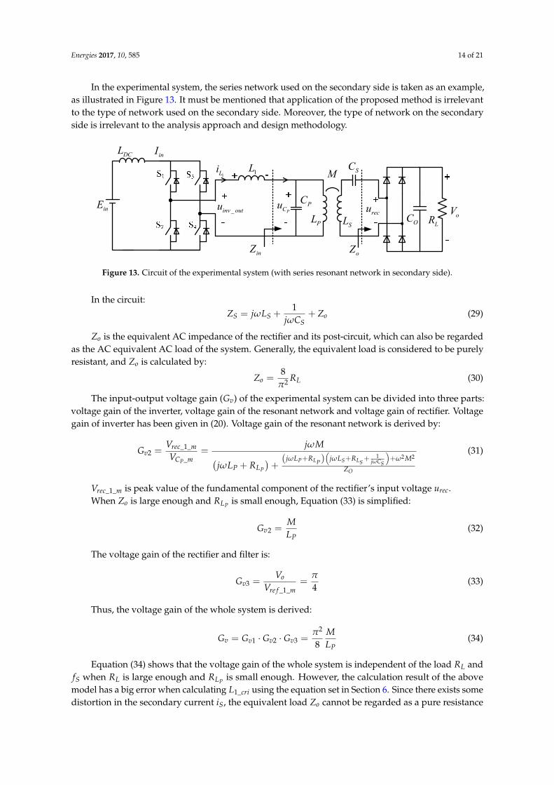
In the experimental system, the series network used on the secondary side is taken as an example,as illustrated in Figure 13. It must be mentioned that application of the proposed method is irrelevantto the type of network used on the secondary side. Moreover, the type of network on the secondaryside is irrelevant to the analysis approach and design methodology.
Energies 2017, 10, 585 14 of 21
LS 60.59 μH RLS 0.093 Ω CS 0.37 μF CO 220 μF RL 10 Ω (rated)
In the experimental system, the series network used on the secondary side is taken as an example, as illustrated in Figure 13. It must be mentioned that application of the proposed method is irrelevant to the type of network used on the secondary side. Moreover, the type of network on the secondary side is irrelevant to the analysis approach and design methodology.
inE
DCL inI
_inv outuPC
u
1Li 1L
inZ
PC
PL SL
SCM
LROCoV
oZ
recu
Figure 13. Circuit of the experimental system (with series resonant network in secondary side).
In the circuit:
1S S o
S
Z j L Zj C
ωω
= + + (29)
oZ is the equivalent AC impedance of the rectifier and its post-circuit, which can also be regarded as the AC equivalent AC load of the system. Generally, the equivalent load is considered to be purely resistant, and oZ is calculated by:
2
8o LZ R
π= (30)
The input-output voltage gain ( vG ) of the experimental system can be divided into three parts: voltage gain of the inverter, voltage gain of the resonant network and voltage gain of rectifier. Voltage gain of inverter has been given in (20). Voltage gain of the resonant network is derived by:
( )( )
_1_2
_ 2 21P
P S
P
rec mv
C mP L S L
SP L
O
V j MG
Vj L R j L R M
j Cj L R
Z
ω
ω ω ωω
ω
= =
+ + + + + +
(31)
_1_rec mV is peak value of the fundamental component of the rectifier’s input voltage recu .
When oZ is large enough andPL
R is small enough, Equation (33) is simplified:
2vP
MG
L= (32)
The voltage gain of the rectifier and filter is:
3_1_ 4o
vref m
VG
V
π= = (33)
Thus, the voltage gain of the whole system is derived:
Figure 13. Circuit of the experimental system (with series resonant network in secondary side).
In the circuit:ZS = jωLS +
1jωCS
+ Zo (29)
Zo is the equivalent AC impedance of the rectifier and its post-circuit, which can also be regardedas the AC equivalent AC load of the system. Generally, the equivalent load is considered to be purelyresistant, and Zo is calculated by:
Zo =8
π2 RL (30)
The input-output voltage gain (Gv) of the experimental system can be divided into three parts:voltage gain of the inverter, voltage gain of the resonant network and voltage gain of rectifier. Voltagegain of inverter has been given in (20). Voltage gain of the resonant network is derived by:
Gv2 =Vrec_1_mVCP_m
=jωM(
jωLP + RLP
)+
(jωLP+RLP)(
jωLS+RLS+1
jωCS
)+ω2 M2
ZO
(31)
Vrec_1_m is peak value of the fundamental component of the rectifier’s input voltage urec.When Zo is large enough and RLP is small enough, Equation (33) is simplified:
Gv2 =MLP
(32)
The voltage gain of the rectifier and filter is:
Gv3 =Vo
Vre f _1_m=
π
4(33)
Thus, the voltage gain of the whole system is derived:
Gv = Gv1 · Gv2 · Gv3 =π2
8MLP
(34)
Equation (34) shows that the voltage gain of the whole system is independent of the load RL andfS when RL is large enough and RLP is small enough. However, the calculation result of the abovemodel has a big error when calculating L1_cri using the equation set in Section 6. Since there exists somedistortion in the secondary current iS, the equivalent load Zo cannot be regarded as a pure resistance
Energies 2017, 10, 585 15 of 21
and simply calculated using Equation (30). Based on the extended fundamental frequency analysismethod [19], a more accurate Zo is derived:
Zo =8LSRLω
−j(π2 − 8)RL + LSπ2ω(35)
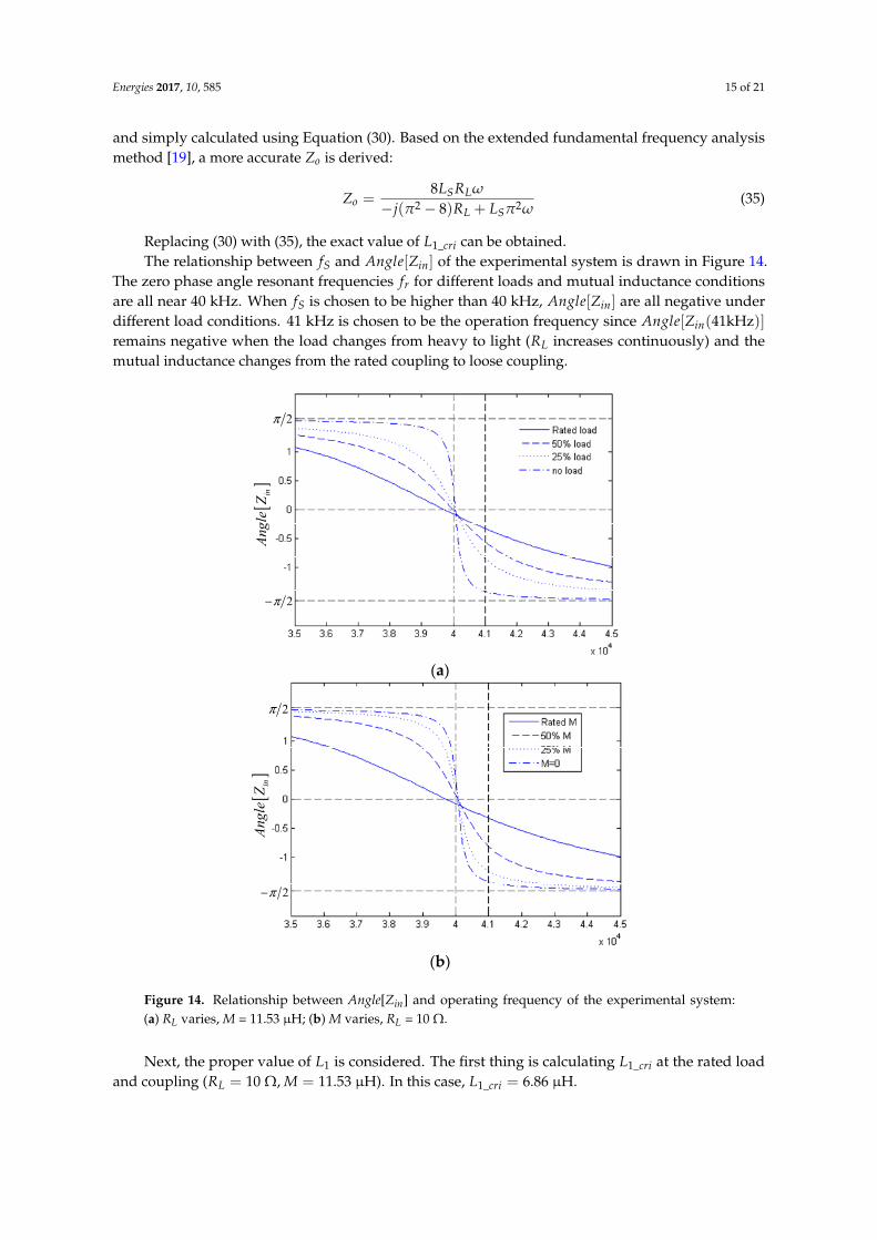
Replacing (30) with (35), the exact value of L1_cri can be obtained.The relationship between fS and Angle[Zin] of the experimental system is drawn in Figure 14.
The zero phase angle resonant frequencies fr for different loads and mutual inductance conditionsare all near 40 kHz. When fS is chosen to be higher than 40 kHz, Angle[Zin] are all negative underdifferent load conditions. 41 kHz is chosen to be the operation frequency since Angle[Zin(41kHz)]remains negative when the load changes from heavy to light (RL increases continuously) and themutual inductance changes from the rated coupling to loose coupling.
Energies 2017, 10, 585 15 of 21
2
1 2 3 8v v v vP
MG G G G
L
π= ⋅ ⋅ = (34)
Equation (34) shows that the voltage gain of the whole system is independent of the load LR and Sf when LR is large enough and
PLR is small enough. However, the calculation result of the
above model has a big error when calculating 1_criL using the equation set in Section 6. Since there
exists some distortion in the secondary current Si , the equivalent load oZ cannot be regarded as a pure resistance and simply calculated using Equation (30). Based on the extended fundamental frequency analysis method [19], a more accurate oZ is derived:
2 2
8( 8)
S Lo
L S
L RZ
j R L
ωπ π ω
=− − +
(35)
Replacing (30) with (35), the exact value of 1_ criL can be obtained.
The relationship between Sf and [ ]inAngle Z of the experimental system is drawn in Figure 14.
The zero phase angle resonant frequencies rf for different loads and mutual inductance conditions
are all near 40 kHz. When Sf is chosen to be higher than 40 kHz, [ ]inAngle Z are all negative under
different load conditions. 41 kHz is chosen to be the operation frequency since ( )41kHzinAngle Z
remains negative when the load changes from heavy to light ( LR increases continuously) and the mutual inductance changes from the rated coupling to loose coupling.
2π−
2π
[]
inAngleZ
(a)
2π−
[]
inAngleZ
2π
(b)
Figure 14. Relationship between Angle[Zin] and operating frequency of the experimental system: (a) RL varies, M = 11.53 μH; (b) M varies, RL = 10 Ω.
Figure 14. Relationship between Angle[Zin] and operating frequency of the experimental system:(a) RL varies, M = 11.53 µH; (b) M varies, RL = 10 Ω.
Next, the proper value of L1 is considered. The first thing is calculating L1_cri at the rated loadand coupling (RL = 10 Ω, M = 11.53 µH). In this case, L1_cri = 6.86 µH.

Energies 2017, 10, 585 16 of 21
Then calculate L1_cri when M and RL vary. The results are shown in Figure 15. When RLvaries from rated load to light load, the correspondent L1_cri increases monotonously. When themutual inductance M varies from rated coupling to weak coupling, the corresponding L1_cri increasesmonotonously. Therefore, if L1_cri is equal to or lower than 6.87 µH, the third operating condition willbe naturally achieved when RL and M vary.
Considering the error of measurement and modeling, L1 needs to be smaller than 6.86 µH toguarantee the third operating condition. In this experimental system, the value of L1 is 3.85 µH.
Energies 2017, 10, 585 16 of 21
Next, the proper value of 1L is considered. The first thing is calculating 1_ criL at the rated load
and coupling ( 10 , 11.53μHLR M= Ω = ). In this case, 1_ 6.86μHcriL = .
Then calculate 1_ criL when M and LR vary. The results are shown in Figure 15. When LR varies from rated load to light load, the correspondent 1_ criL increases monotonously. When the mutual inductance M varies from rated coupling to weak coupling, the corresponding 1_ criL increases monotonously. Therefore, if 1_ criL is equal to or lower than 6.87 μH, the third operating
condition will be naturally achieved when LR and M vary. Considering the error of measurement and modeling, 1L needs to be smaller than 6.86 μH to
guarantee the third operating condition. In this experimental system, the value of 1L is 3.85 μH.
(a)
(b)
Figure 15. The critical value L1_cri: (a) RL varies, M = 11.53 μH; (b) M varies, RL = 10 Ω.
7.3. Experiment and Performance
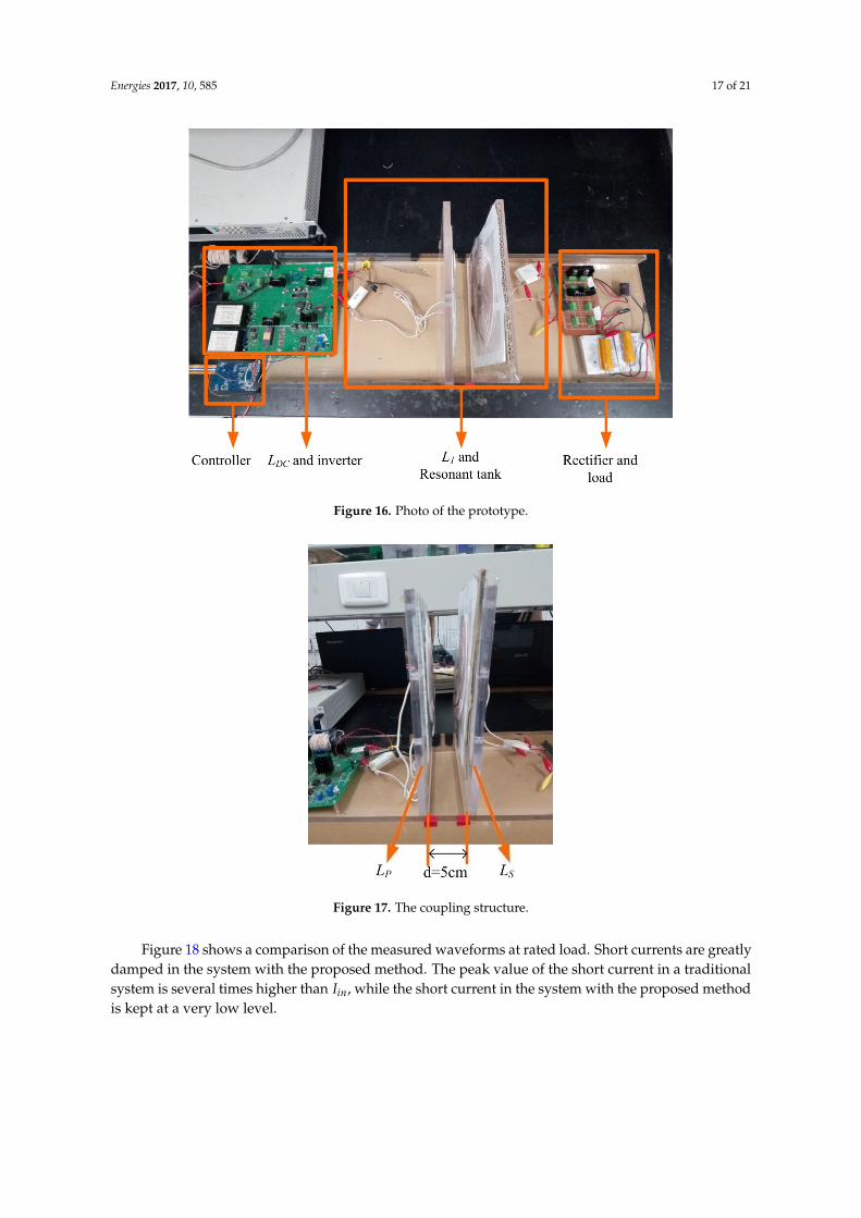
A proposed 60 W Current-Fed WPT prototype is built to verify the method. The experimental system is set up as shown in Figure 13. The switching components used are IGBT FGA25N120ANTD and STPS20120D diodes. The driving signals are produced by a TMS320X2812 DSP. Photos of the prototype system are shown in Figures 16 and 17.
Figure 15. The critical value L1_cri: (a) RL varies, M = 11.53 µH; (b) M varies, RL = 10 Ω.
7.3. Experiment and Performance
A proposed 60 W Current-Fed WPT prototype is built to verify the method. The experimentalsystem is set up as shown in Figure 13. The switching components used are IGBT FGA25N120ANTDand STPS20120D diodes. The driving signals are produced by a TMS320X2812 DSP. Photos of theprototype system are shown in Figures 16 and 17.
Energies 2017, 10, 585 17 of 21
Energies 2017, 10, 585 17 of 21
Figure 16. Photo of the prototype.
Figure 17. The coupling structure.
Figure 18 shows a comparison of the measured waveforms at rated load. Short currents are greatly damped in the system with the proposed method. The peak value of the short current in a traditional system is several times higher than inI , while the short current in the system with the proposed method is kept at a very low level.
Figure 16. Photo of the prototype.
Energies 2017, 10, 585 17 of 21
Figure 16. Photo of the prototype.
Figure 17. The coupling structure.
Figure 18 shows a comparison of the measured waveforms at rated load. Short currents are greatly damped in the system with the proposed method. The peak value of the short current in a traditional system is several times higher than inI , while the short current in the system with the proposed method is kept at a very low level.
Figure 17. The coupling structure.
Figure 18 shows a comparison of the measured waveforms at rated load. Short currents are greatlydamped in the system with the proposed method. The peak value of the short current in a traditionalsystem is several times higher than Iin, while the short current in the system with the proposed methodis kept at a very low level.

Energies 2017, 10, 585 18 of 21Energies 2017, 10, 585 18 of 21
(a)
(b)
(c)
Figure 18. Short current control performance comparison: (a) Traditional parallel WPT system under heavy load condition ( LR = 10 Ω); (b) Short current control performance with 1L = 3.45 μH, LR =
10 Ω; (c) Short current control performance with 1L = 6.40 μH, LR = 10 Ω.
Due to parasitic capacitance in the switches and junction capacitors in their anti-parallel diode, a current oscillation exists in
1Li after t4. Figure 18c illustrates the waveform of the system with the
proposed approach when 1L = 6.40 μH. In this situation, the peak value of the short current is nearly equal to Iin, which verifies the accuracy of the model in Section 6. As shown in Figure 18b, 3.45 μH is a proper value of 1L , so in the remaining experiments, 1L is chosen to be 3.45 μH.
Figure 18. Short current control performance comparison: (a) Traditional parallel WPT system underheavy load condition (RL = 10 Ω); (b) Short current control performance with L1 = 3.45 µH, RL = 10 Ω;(c) Short current control performance with L1 = 6.40 µH, RL = 10 Ω.
Due to parasitic capacitance in the switches and junction capacitors in their anti-parallel diode,a current oscillation exists in iL1 after t4. Figure 18c illustrates the waveform of the system with theproposed approach when L1 = 6.40 µH. In this situation, the peak value of the short current is nearlyequal to Iin, which verifies the accuracy of the model in Section 6. As shown in Figure 18b, 3.45 µH is aproper value of L1, so in the remaining experiments, L1 is chosen to be 3.45 µH.
Detailed waveforms of the proposed system are shown in Figure 19. As described in Section 5,the switches turn off in the zero-crossing point of uCp. The overlap time Tov is regulated automaticallyand the operation conditions are satisfied.

Energies 2017, 10, 585 19 of 21
Energies 2017, 10, 585 19 of 21
Detailed waveforms of the proposed system are shown in Figure 19. As described in Section 5, the switches turn off in the zero-crossing point of uCp. The overlap time Tov is regulated automatically and the operation conditions are satisfied.
Tov
ug1/ug4:[20V/div]
ug2/ug3:[20V/div]
iL1:[2A/div]
uCp:[50V/div]
Figure 19. The switching waveform during the commutation period (when LR = 10 Ω, 1L = 3.45 μH).
Figure 20 shows waveforms of one switch. During the turn-on time, the current of switch iS equals to 0 and slowly increases, which means ZCS is achieved. At turn-off time, the voltage of the switch uCp remains at zero and ZVS are achieved. Because of these excellent properties, loss of switching devices in the system can be greatly reduced, that is, the efficiency will be enhanced. When the distances of LP and LS increase, the system still operates normally, as shown in Figure 21.
Figure 20. Waveform of switch (when LR = 10 Ω, 1L = 3.45 μH).
ug1/ug4:[20V/div]
ug2/ug3:[20V/div]
iinv_out:[2A/div]
(a) (b)
Figure 19. The switching waveform during the commutation period (when RL = 10 Ω, L1 = 3.45 µH).
Figure 20 shows waveforms of one switch. During the turn-on time, the current of switch iS equalsto 0 and slowly increases, which means ZCS is achieved. At turn-off time, the voltage of the switch uCp
remains at zero and ZVS are achieved. Because of these excellent properties, loss of switching devicesin the system can be greatly reduced, that is, the efficiency will be enhanced. When the distances of LPand LS increase, the system still operates normally, as shown in Figure 21.
Energies 2017, 10, 585 19 of 21
Detailed waveforms of the proposed system are shown in Figure 19. As described in Section 5, the switches turn off in the zero-crossing point of uCp. The overlap time Tov is regulated automatically and the operation conditions are satisfied.
Tov
ug1/ug4:[20V/div]
ug2/ug3:[20V/div]
iL1:[2A/div]
uCp:[50V/div]
Figure 19. The switching waveform during the commutation period (when LR = 10 Ω, 1L = 3.45 μH).
Figure 20 shows waveforms of one switch. During the turn-on time, the current of switch iS equals to 0 and slowly increases, which means ZCS is achieved. At turn-off time, the voltage of the switch uCp remains at zero and ZVS are achieved. Because of these excellent properties, loss of switching devices in the system can be greatly reduced, that is, the efficiency will be enhanced. When the distances of LP and LS increase, the system still operates normally, as shown in Figure 21.
Figure 20. Waveform of switch (when LR = 10 Ω, 1L = 3.45 μH).
ug1/ug4:[20V/div]
ug2/ug3:[20V/div]
iinv_out:[2A/div]
(a) (b)
Figure 20. Waveform of switch (when RL = 10 Ω, L1 = 3.45 µH).
Energies 2017, 10, 585 19 of 21
Detailed waveforms of the proposed system are shown in Figure 19. As described in Section 5, the switches turn off in the zero-crossing point of uCp. The overlap time Tov is regulated automatically and the operation conditions are satisfied.
Tov
ug1/ug4:[20V/div]
ug2/ug3:[20V/div]
iL1:[2A/div]
uCp:[50V/div]
Figure 19. The switching waveform during the commutation period (when LR = 10 Ω, 1L = 3.45 μH).
Figure 20 shows waveforms of one switch. During the turn-on time, the current of switch iS equals to 0 and slowly increases, which means ZCS is achieved. At turn-off time, the voltage of the switch uCp remains at zero and ZVS are achieved. Because of these excellent properties, loss of switching devices in the system can be greatly reduced, that is, the efficiency will be enhanced. When the distances of LP and LS increase, the system still operates normally, as shown in Figure 21.
Figure 20. Waveform of switch (when LR = 10 Ω, 1L = 3.45 μH).
ug1/ug4:[20V/div]
ug2/ug3:[20V/div]
iinv_out:[2A/div]
(a) (b)
Figure 21. Steady-state waveform when M varies (RL = 10 Ω, L1 = 3.45 µH): (a) 6 cm, M = 8.77 µH;(b) 7 cm, M = 6.70 µH.

Energies 2017, 10, 585 20 of 21
To verify the theoretical model, a set of experimental data was measured. The experimental andtheoretical voltage gains are compared in Figure 22.
Energies 2017, 10, 585 20 of 21
Figure 21. Steady-state waveform when M varies ( LR = 10 Ω, 1L = 3.45 μH): (a) 6 cm, M = 8.77 μH;
(b) 7 cm, M = 6.70 μH.
To verify the theoretical model, a set of experimental data was measured. The experimental and theoretical voltage gains are compared in Figure 22.
Figure 22. Comparison of theoretical value and experimental data of vG .
The efficiency of traditional parallel WPT system and new WPT system is compared in Figure 23. During large load variation, efficiency of proposed system is always higher than traditional system due to short current is effectively controlled.
Figure 23. Efficiency of traditional system and proposed system.
8. Conclusions
Short currents occur in WPT systems when the operation frequency drifts from the inherent frequency of the resonant network. This phenomenon is quite dangerous for switching components and other circuit components. This paper proposes a novel method, named inductance-damping method, based on utilizing an additional small inductance to inhibit short currents. Steady-state mode and operating conditions are analyzed. An overlapping time regulation circuit is given and the range of vG is discussed. The system design procedure is described and a design example is discussed. The experimental waveforms and data are given to verify the method. Furthermore, this method can be extended to Current-Fed full-resonant converters.
Figure 22. Comparison of theoretical value and experimental data of Gv.
The efficiency of traditional parallel WPT system and new WPT system is compared in Figure 23.During large load variation, efficiency of proposed system is always higher than traditional systemdue to short current is effectively controlled.
Energies 2017, 10, 585 20 of 21
Figure 21. Steady-state waveform when M varies ( LR = 10 Ω, 1L = 3.45 μH): (a) 6 cm, M = 8.77 μH;
(b) 7 cm, M = 6.70 μH.
To verify the theoretical model, a set of experimental data was measured. The experimental and theoretical voltage gains are compared in Figure 22.
Figure 22. Comparison of theoretical value and experimental data of vG .
The efficiency of traditional parallel WPT system and new WPT system is compared in Figure 23. During large load variation, efficiency of proposed system is always higher than traditional system due to short current is effectively controlled.
Figure 23. Efficiency of traditional system and proposed system.
8. Conclusions
Short currents occur in WPT systems when the operation frequency drifts from the inherent frequency of the resonant network. This phenomenon is quite dangerous for switching components and other circuit components. This paper proposes a novel method, named inductance-damping method, based on utilizing an additional small inductance to inhibit short currents. Steady-state mode and operating conditions are analyzed. An overlapping time regulation circuit is given and the range of vG is discussed. The system design procedure is described and a design example is discussed. The experimental waveforms and data are given to verify the method. Furthermore, this method can be extended to Current-Fed full-resonant converters.
Figure 23. Efficiency of traditional system and proposed system.
8. Conclusions
Short currents occur in WPT systems when the operation frequency drifts from the inherentfrequency of the resonant network. This phenomenon is quite dangerous for switching componentsand other circuit components. This paper proposes a novel method, named inductance-dampingmethod, based on utilizing an additional small inductance to inhibit short currents. Steady-state modeand operating conditions are analyzed. An overlapping time regulation circuit is given and the rangeof Gv is discussed. The system design procedure is described and a design example is discussed.The experimental waveforms and data are given to verify the method. Furthermore, this method canbe extended to Current-Fed full-resonant converters.
Acknowledgments: The research work is financially supported by the research fund of National Natural ScienceFoundation of China (Nos. 51377183, 51377187).

Energies 2017, 10, 585 21 of 21
Author Contributions: Author Yanling Li implemented the research, performed the analysis, experimental dataanalysis and wrote the paper. Author Qichang Duan contributed the main idea of this paper and providedguidance and supervision. Author Weiyi Li carried out experimental tests.
Conflicts of Interest: The authors declare no conflict of interest.
References
1. Villa, J.L.; Sallan, J.; Osorio, J.F.S.; Llombart, A. High-misalignment tolerant compensation topology for ICPTsystems. IEEE Trans. Ind. Electron. 2012, 59, 945–951. [CrossRef]
2. Zhang, W.; Wong, S.C.; Chi, K.T.; Chen, Q. Design for efficiency optimization and voltage controllability ofseries—Series compensated inductive power transfer systems. IEEE Trans. Power Electron. 2014, 29, 191–200.[CrossRef]
3. Pantic, Z.; Lukic, S.M. Framework and topology for active tuning of parallel compensated receivers in powertransfer systems. IEEE Trans. Power Electron. 2012, 27, 4503–4513. [CrossRef]
4. Thrimawithana, D.J.; Madawala, U.K. A generalized steady-state model for bidirectional IPT systems.IEEE Trans. Power Electron. 2013, 28, 4681–4689. [CrossRef]
5. Huang, C.Y.; Boys, J.T.; Covic, G.A. LCL pickup circulating current controller for inductive power transfersystems. IEEE Trans. Power Electron. 2013, 28, 2081–2093. [CrossRef]
6. Madawala, U.K.; Neath, M.; Thrimawithana, D.J. A power–frequency controller for bidirectional inductivepower transfer systems. IEEE Trans. Ind. Electron. 2013, 60, 310–317. [CrossRef]
7. Chen, R.Y.; Liang, T.J.; Chen, J.F.; Lin, R.L.; Tseng, K.C. Study and implementation of a current-fed full-bridgeboost DC—DC converter with zero-current switching for high-voltage applications. IEEE Trans. Ind. Appl.2008, 44, 1218–1226. [CrossRef]
8. Yuan, B.; Yang, X.; Zeng, X.; Duan, J.; Zhai, J.; Li, D. Analysis and design of a high step-up current-fedmultiresonant DC–DC converter with low circulating energy and zero-current switching for all activeswitches. IEEE Trans. Ind. Electron. 2012, 59, 964–978. [CrossRef]
9. Hu, A.P. Selected Resonant Converters for IPT Power Supplies. Ph.D. Thesis, Department of Electrical andComputer Engineering, Auckland University, Auckland, New Zealand, 2001.
10. Si, P.; Hu, A.P.; Malpas, S.; Budgett, D. A frequency control method for regulating wireless power toimplantable devices. IEEE Trans. Biomed. Circuits Syst. 2008, 2, 22–29. [CrossRef] [PubMed]
11. Hu, A.P.; Boys, J.T.; Covic, G.A. Frequency analysis and computation of a current-fed resonant converter forICPT power supplies. In Proceedings of the International Conference on Power System Technology, Perth,Australia, 4–7 December 2000; pp. 327–332.
12. Tang, C.S.; Sun, Y.; Su, Y.G.; Nguang, S.K.; Hu, A.P. Determining multiple steady-state ZCS operating pointsof a switch-mode contactless power transfer system. IEEE Trans. Power Electron. 2015, 24, 416–425. [CrossRef]
13. Su, Y.G.; Zhang, H.Y.; Wang, Z.H.; Hu, A.P. Steady-state load identification method of inductive powertransfer system based on switching capacitors. IEEE Trans. Power Electron. 2015, 30, 6349–6355. [CrossRef]
14. Wang, Z.H.; Li, Y.P.; Sun, Y.; Tang, C.S.; Lv, X. Load detection model of voltage-fed inductive power transfersystem. IEEE Trans. Power Electron. 2013, 28, 5233–5243. [CrossRef]
15. Hu, A.P.; Covic, G.A.; Boys, J.T. Direct ZVS start-up of a current-fed resonant inverter. IEEE Trans.Power Electron. 2006, 21, 809–812. [CrossRef]
16. Dai, X.; Sun, Y. An accurate frequency tracking method based on short current detection for inductive powertransfer system. IEEE Trans. Ind. Electron. 2014, 61, 776–783. [CrossRef]
17. Namadmalan, A. Bidirectional current-fed resonant Inverter for contactless energy transfer systems.IEEE Trans. Ind. Electron. 2015, 62, 238–245. [CrossRef]
18. Yan, K.; Chen, Q.; Hou, J.; Ren, X.; Ruan, X. Self-oscillating contactless resonant converter with phasedetection contactless current transformer. IEEE Trans. Power Electron. 2014, 29, 4438–4449. [CrossRef]
19. Forsyth, A.J.; Ward, G.A.; Mollov, S.V. Extended fundamental frequency analysis of the LCC resonantconverter. IEEE Trans. Power Electron. 2003, 18, 1286–1292. [CrossRef]
© 2017 by the authors. Licensee MDPI, Basel, Switzerland. This article is an open accessarticle distributed under the terms and conditions of the Creative Commons Attribution(CC BY) license (http://creativecommons.org/licenses/by/4.0/).