a self-amplifying four-transistor mosfet mismatch test structure
TRANSCRIPT
IEEE TRANSACTIONS ON SEMICONDUCTOR MANUFACTURING, VOL. 26, NO. 3, AUGUST 2013 273
A Self-Amplifying Four-Transistor MOSFETMismatch Test Structure
Colin C. McAndrew, Fellow, IEEE, Mike Zunino, and Brandt Braswell
Abstract—Mismatch can be difficult to monitor in a productiontest environment as it can be small and, therefore, it requiresprecise, time-consuming, costly measurements. This paper de-scribes a four-transistor test structure for measurement andcharacterization of MOS transistor mismatch that self-amplifiesthe effect of mismatch, thereby generating a large and easilymeasurable dc output voltage. Test and design aspects of thestructure are detailed, and several additional applications of thenew structure are described.
Index Terms—CMOS analog integrated circuits, semiconduc-tor device modeling, semiconductor device testing, SPICE.
I. Introduction
IN INTEGRATED circuit (IC) manufacturing technologiesprecision analog circuit design based on absolute
component values is difficult because statistical variationsin these values can be as large as ±20%. Trim or off-chipcomponents can be used to achieve tight tolerances for circuitperformance, but both entail additional cost. Even thoughabsolute component variability is large, the relative differencein component value between adjacent devices on the sameIC is small, and can be controlled by adjusting device size,layout, and bias. Differential design techniques based on(ideally) identical devices are therefore widely used forprecision analog and RF circuits.
The degree of difference between devices, called local varia-tion or mismatch, is due to unavoidable atomistic variations inthe physical structure of each device, e.g., line edge roughness(LER) [1], [2] and random dopant fluctuation (RDF) [3]–[6]. Although mismatch is often considered to be a pairwisephenomena it actually arises from atomistic fluctuations thataffect each device individually and, unlike global (wafer-to-wafer and lot-to-lot) variations, are uncorrelated betweendevices. The total statistical variance of a process parameterpi for one device is
σ2pi,total = σ2
pi,global + σ2pi,local(L, W, . . . ) (1)
where the local variation depends on device geometric layoutparameters such as length L and width W . The mismatch inpi between two devices, labeled 1 and 2, is then
σ2�pi
= σ2pi,local(L1, W1, . . . ) + σ2
pi,local(L2, W2, . . . ) . (2)
Manuscript received September 28, 2012; revised January 07, 2013;accepted April 08, 2013. Date of publication April 12, 2013; date of currentversion July 31, 2013.
The authors are with Freescale Semiconductor Inc., Tempe, AZ 85284 USA(e-mail: [email protected]; [email protected];[email protected]).
Digital Object Identifier 10.1109/TSM.2013.2257896
Local variation standard deviations have a reciprocal depen-dence on geometry [7], [8], increasing as device size decreases,and the inexorable scaling of CMOS technologies has meantthat since about the 130-nm technology node the local com-ponent of variation has exceeded the global component ofvariation for minimum size devices [9], [10]. Mismatch istherefore now of significant concern for digital, as well asanalog and RF CMOS ICs.
Characterization and modeling of MOS transistor mismatchfor design can be done via model parameters such as zero-bias threshold voltage VT0 and gain factor β = μ0C
′oxW/L
[7], [8], where μ0 is low-field mobility and C′ox is oxide
capacitance per unit area, which need to be calculated fromdevice measurements. An alternative is to model mismatchusing independent physical parameters, e.g., substrate dopingN, oxide thickness tox, and channel length and width variation�L and �W , respectively, and to characterize these modelsusing backward propagation of variance (BPV) from directmeasurement of mismatch in drain current ID over bias andgeometry [11]. In either case, because MOS transistors matchwell (to better than 1% for large devices) characterization ofmismatch requires careful measurement.
Significant research has been done on test structures andprecision measurement techniques for mismatch; an excellentand comprehensive overview, with an extensive bibliography,is available in [12]. To quote from that reference: “In themost general sense, it can stated that (mismatch) measurementaccuracy can be traded-in for measurement speed.” For accu-rate technology characterization and modeling of mismatch,to support technology optimization and IC design, carefullaboratory measurements are indispensable. However, giventhe sensitivity of both analog and digital ICs to mismatch,it is also desirable to monitor MOS transistor mismatch inmanufacturing. Unfortunately, not only are production testsystems often less capable than laboratory test systems, buttest can be a significant contributor to overall manufacturingcost, so there is continual pressure to minimize test time. Itwould therefore be useful to have a structure than can be easilyand quickly measured, in a manufacturing test environment,to track MOS transistor mismatch. This paper describes astructure targeted for that purpose.
The paper proceeds as follows. In Section II we present thetest structure, then analyze how it works and describe howit should be measured in Sections III and IV, respectively.Section V presents experimental results that verify the opera-tion of the structure. Further application areas are discussed in
0894-6507/$31.00 c© 2013 IEEE
274 IEEE TRANSACTIONS ON SEMICONDUCTOR MANUFACTURING, VOL. 26, NO. 3, AUGUST 2013
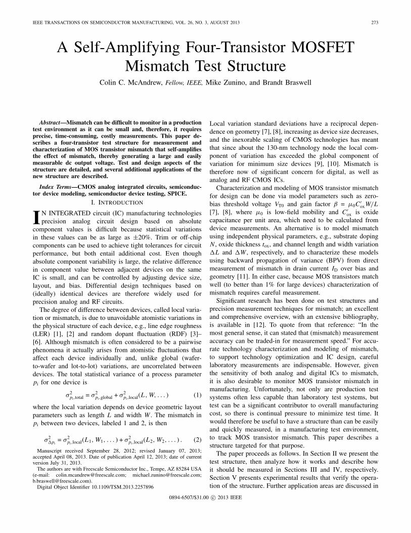
Fig. 1. New four-transistor MOS mismatch structure.
Section VI, and conclusions are presented in Section VII. Thestructure was first described in [13] and here we extend thatwork by providing a detailed theoretical circuit analysis, circuitsimulation results, and additional experimental results. Allmeasurements are from structures based on medium voltagenMOS and pMOS transistors in a 0.25μm power BiCMOSprocess [14], from 14 wafers from two separate lots. Struc-tures with varying transistor geometries were measured, andthere are approximately 520 individual measurements for eachgeometry (data from a few bad sites were filtered out).
II. The 4-Transistor Structure
Fig. 1 shows the new MOS mismatch structure, whichconsists of two CMOS inverters connected in series. The firststage (on the left side of Fig. 1) has its output connected to itsinput. In essence it is a self-biasing CMOS voltage referencecircuit, although not a particularly good one as its outputvoltage V1 varies directly with the supply voltage VDD [15];this turns out to be serendipitous for our purpose.
If the nMOS and pMOS transistors of the second stage (onthe right side of Fig. 1) are electrically identical to those ofthe first stage then, just like for that stage, its output voltagemust equal its input voltage, hence
�V = V2 − V1 (3)
must be zero. However, if there is mismatch between transis-tors �V will be non-zero. The self-biasing point of the firststage makes the second stage act not as a digital inverter butas an analog amplifier, and it operates at, or very close to,the point of maximum voltage gain; see Fig. 2. The secondstage therefore causes the overall test structure to self-amplifythe effect of any transistor mismatch between the first andsecond stages. The signal �V is directly proportional to thetransistor mismatch and, because of the amplification by thesecond stage, should have a large, easily measurable dc value.
III. Theoretical Analysis
Assuming ideal square-law behavior of the MOS transistorsin the first stage of Fig. 1 their drain currents are
IDn =βn
2(V1 − VT0n)2 = IDp =
βp
2(VDD − V1 − VT0p)2 (4)
Fig. 2. Simulated CMOS inverter V2(V1) transfer characteristic and small-signal gain; Wn/Ln = 2Wmin/2Lmin and Wp/Lp = 6Wmin/2Lmin. (a) Self-biasing point is where V2 = V1. (b) Blow-up of (a) around the self-biasingpoint.
therefore the voltage V1 is
V1 =VDD − VT0p +
√βn/βpVT0n
1 +√
βn/βp
, (5)
where the added subscripts n and p indicate a quantity isfor the nMOS or pMOS transistor, respectively, and VT0p isconsidered positive for an enhancement mode transistor. Ifthese transistors are balanced, so that βn = βp and VT0n = VT0p,then V1 = VDD/2, as could be expected.
If we assume, as in [7] and [8], that mismatch is modeledvia perturbations in the gain factors and zero-bias thresholdvoltages, then the mismatch variation in V1 is
δV1 ≈√
βn/βpδVT0n − δVT0p
1 +√
βn/βp
− VDDO
2(1 +√
βn/βp)2
√βn
βp
(δβn
βn
− δβp
βp
)(6)
where the supply voltage overdrive is
VDDO = VDD − VT0n − VT0p . (7)
The small-signal voltage gain of the second stage amplifier is
AV =∂V2
∂V1= −gmn + gmp
gon + gop
(8)
MCANDREW et al.: A SELF-AMPLIFYING FOUR-TRANSISTOR MOSFET MISMATCH TEST STRUCTURE 275
Fig. 3. Simulated inverter voltage gain at the self-bias point.
where gm and go denote small-signal transconductance∂ID/∂VG and output conductance ∂ID/∂VD, respectively. Thelocal variations in the transistors of both stages contributeto variations in �V , and from symmetry the magnitude ofthe contribution from first and second stage transistors is thesame (e.g., a shift of +δVT0n in transistor MN1 is equivalentto a shift of −δVT0n in transistor MN2; circuit simulationsverify this equivalence). Therefore there are two independentcontributions like (6) to the effective variation in V1, andapplying the voltage gain of the second stage amplifier gives
σ2�V = (|AV | + 1)2
[σ2
δVT0p
2+
σ2δVT0n
2
+V 2
DDO
32
(σ2
δβn/βn+ σ2
δβp/βp
)](9)
for the case of balanced nMOS and pMOS transistors [thevariances in (9) are for the local component of variation].
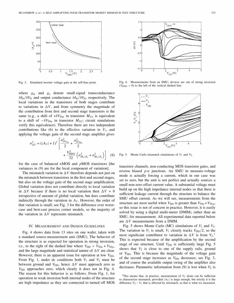
The mismatch variation in �V therefore depends not just onthe mismatch between transistors in the first and second stages,but also on the voltage gain of the second stage amplification.Global variation does not contribute directly to local variationin �V because if there is no local variation then �V = 0irrespective of amount of global variation, but does contributeindirectly through the variation in AV . However, the order ofthat variation is small; see Fig. 3 for the difference over worst-case and best-cast process corner models, so the majority ofthe variation in �V represents mismatch.
IV. Measurement and Design Guidelines
Fig. 4 shows data from 13 sites on one wafer, taken witha standard source-measurement unit (SMU). The behavior ofthe structure is as expected for operation in strong inversion,i.e., to the right of the dashed line where VDD > VT0n + VT0p,and the large magnitude and statistical nature of �V are clear.However, there is an apparent issue for operation at low VDD.From Fig. 1, under dc conditions both V1 and V2 must bebetween ground and VDD, hence �V must approach zero asVDD approaches zero, which clearly it does not in Fig. 4.The reason for this behavior is as follows. From Fig. 1, foroperation in weak inversion both internal nodes of the structureare high impedance as they are connected to turned off MOS
Fig. 4. Measurements from an SMU; devices are out of strong inversion(VDDO < 0) to the left of the vertical dashed line.
Fig. 5. Monte Carlo mismatch simulations of V1 and V2.
transistor channels, non-conducting MOS transistor gates, andreverse biased p-n junctions. An SMU in measure-voltagemode is actually forcing a current, which in our case wasset to zero, but the unit is not perfect and actually sources asmall non-zero offset current value. A substantial voltage mustbuild up on the high impedance internal nodes so that there issufficient leakage current through the structure to balance theSMU offset current. As we will see, measurements from thestructure are most useful when VDD is greater than VT0n +VT0p,so this issue is not of concern in practice. However, it is easilysolved by using a digital multi-meter (DMM), rather than anSMU, for measurement. All experimental data reported beloware �V measurements from a DMM.
Fig. 5 shows Monte Carlo (MC) simulations of V1 and V2.The variation in V1 is small, V1 closely tracks VDD/2, so themost significant contributor to variation in �V is from V2.1
This is expected because of the amplification by the secondstage of our structure. Until VDD is sufficiently large Fig. 5shows that V2 is close to one of the supply rails, groundor VDD. This is because the magnitude of the voltage gainof the second stage increases as VDD decreases; see Fig. 3,and of course the available output swing of the amplifier alsodecreases. Parametric information from (9) is lost when V2 is
1This means that, in practice, measurement of V2 alone can be sufficientto characterize mismatch, provided |AV | is large enough, but strictly it is thedifference V2 −V1 that is affected by mismatch, so that is what we measured.
276 IEEE TRANSACTIONS ON SEMICONDUCTOR MANUFACTURING, VOL. 26, NO. 3, AUGUST 2013
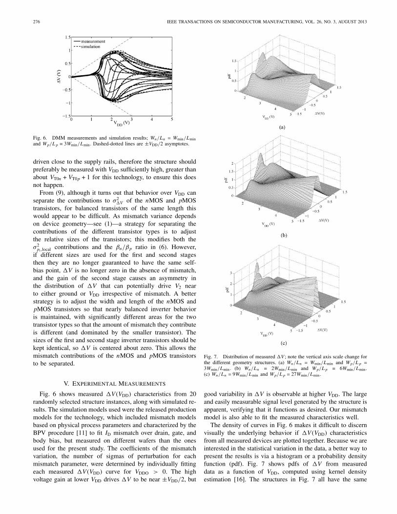
Fig. 6. DMM measurements and simulation results; Wn/Ln = Wmin/Lminand Wp/Lp = 3Wmin/Lmin. Dashed-dotted lines are ±VDD/2 asymptotes.
driven close to the supply rails, therefore the structure shouldpreferably be measured with VDD sufficiently high, greater thanabout VT0n + VT0p + 1 for this technology, to ensure this doesnot happen.
From (9), although it turns out that behavior over VDD canseparate the contributions to σ2
�V of the nMOS and pMOStransistors, for balanced transistors of the same length thiswould appear to be difficult. As mismatch variance dependson device geometry—see (1)—a strategy for separating thecontributions of the different transistor types is to adjustthe relative sizes of the transistors; this modifies both theσ2
pi,local contributions and the βn/βp ratio in (6). However,if different sizes are used for the first and second stagesthen they are no longer guaranteed to have the same self-bias point, �V is no longer zero in the absence of mismatch,and the gain of the second stage causes an asymmetry inthe distribution of �V that can potentially drive V2 nearto either ground or VDD irrespective of mismatch. A betterstrategy is to adjust the width and length of the nMOS andpMOS transistors so that nearly balanced inverter behavioris maintained, with significantly different areas for the twotransistor types so that the amount of mismatch they contributeis different (and dominated by the smaller transistor). Thesizes of the first and second stage inverter transistors should bekept identical, so �V is centered about zero. This allows themismatch contributions of the nMOS and pMOS transistorsto be separated.
V. Experimental Measurements
Fig. 6 shows measured �V (VDD) characteristics from 20randomly selected structure instances, along with simulated re-sults. The simulation models used were the released productionmodels for the technology, which included mismatch modelsbased on physical process parameters and characterized by theBPV procedure [11] to fit ID mismatch over drain, gate, andbody bias, but measured on different wafers than the onesused for the present study. The coefficients of the mismatchvariation, the number of sigmas of perturbation for eachmismatch parameter, were determined by individually fittingeach measured �V (VDD) curve for VDDO > 0. The highvoltage gain at lower VDD drives �V to be near ±VDD/2, but
Fig. 7. Distribution of measured �V ; note the vertical axis scale change forthe different geometry structures. (a) Wn/Ln = Wmin/Lmin and Wp/Lp =3Wmin/Lmin. (b) Wn/Ln = 2Wmin/Lmin and Wp/Lp = 6Wmin/Lmin.(c) Wn/Ln = 9Wmin/Lmin and Wp/Lp = 27Wmin/Lmin.
good variability in �V is observable at higher VDD. The largeand easily measurable signal level generated by the structure isapparent, verifying that it functions as desired. Our mismatchmodel is also able to fit the measured characteristics well.
The density of curves in Fig. 6 makes it difficult to discernvisually the underlying behavior if �V (VDD) characteristicsfrom all measured devices are plotted together. Because we areinterested in the statistical variation in the data, a better way topresent the results is via a histogram or a probability densityfunction (pdf). Fig. 7 shows pdfs of �V from measureddata as a function of VDD, computed using kernel densityestimation [16]. The structures in Fig. 7 all have the same

MCANDREW et al.: A SELF-AMPLIFYING FOUR-TRANSISTOR MOSFET MISMATCH TEST STRUCTURE 277
Fig. 8. Simulated gain-mismatch product versus channel length (normal-ized).
Fig. 9. Distribution of measured �V ; Wn/Ln = Wmin/2Lmin and Wp/Lp =3Wmin/2Lmin. Compare with Fig. 7(a).
(minimum) channel length and balanced nMOS and pMOSdrive strengths, but different channel widths. For low VDD,slightly above VTOn + VTOp = 1.9 V, the pdf shapes are clearlybimodal, as �V is forced to be near ±VDD/2 from the largesecond stage amplification. However, as VDD increases a clearGaussian shape emerges; again, the structure is working asintended.
AV is only weakly dependent on channel width, and mis-match decreases as W increases, so from (9) σ�V shoulddecrease as W increases, precisely as Fig. 7 shows; quantita-tively the decrease has close to the expected 1/
√W behavior.
Over the range of biases of Fig. 7, the decrease in AV withincreasing VDD (roughly a factor of 1/4; see Fig. 3) is morethan offset by the increase in VDDO (roughly a factor of 6),therefore from (9); because σ�V has not yet begun to increasewith increasing VDD at the highest supply voltage values ofFig. 7, the variability in �V is predominantly from thresholdvoltage, and not gain factor, mismatch.
AV varies significantly with channel length. The channelaspect ratio W/L affects transistor ID, but cancels betweenthe gm and go components in the ratio in (8). However, drain-induced barrier lowering and channel length modulation causethe output resistance ro = 1/go to increase at least linearlywith L [17]. For constant W , mismatch standard deviationdecreases approximately as 1/
√L; therefore the voltage gain
increases faster as L increases than mismatch decreases; see
Fig. 10. Distribution of measured �V . First stage Wn/Ln = Wmin/Lmin andWp/Lp = 3Wmin/Lmin. Second stage has same L and nine times W of firststage.
Fig. 8, hence σ�V should increase as L increases. Fig. 9, whichis for devices of twice the length of those of Fig. 7(a), verifiesthis; note also that the bimodal lobes in Fig. 9 at lower VDD
are more pronounced than those of the (same W , shorter L)structure of Fig. 7(a), because the greater |AV | causes V2 tobe forced closer to the supply rails. The distribution spreadseven further for longer devices [13]. This does not mean thatthe structure is incapable of quantitatively characterizing σ�V
if the gain AV , or more precisely the gain-mismatch product,is too high. Although excessive gain can force instances ofthe structure to have outputs that are compressed becausethey are close to ±VDD/2, and so the pdf is non-Gaussianin shape, the interquartile range of �V , or the proportion of�V values between VDD/4 and 3VDD/4, for example, can stillbe used to quantitatively track its variability, and decide whena manufacturing process drifts out of specification.
Fig. 10 shows pdfs of �V as a function of VDD for astructure with asymmetry between the second and first stagetransistors; the first stage had devices of the same geometriesas those of Fig. 7(a) and the second stage devices had theirwidth scaled to nine times those of the first stage, to try toisolate the effects of mismatch in the first stage transistorsfrom those in the second stage. Clearly the distribution isskewed and does not have a zero mean, especially for lowerVDD. This reinforces, as discussed in Section IV, that for thepurpose of trying to isolate the main root physical sourcesof mismatch it is better to differentially size the nMOS andpMOS transistors rather than differentially size the first andsecond stage transistors (we had not realized this when thetest structures were laid out, so only had tried the former andnot the latter).
Although the overall �V output depends on local variationin all devices in the structure, not just from one device orbetween a pair of devices of the same type and geometry, it isstill possible to extract mismatch models from the measureddata. Fig. 11 shows measured and modeled pdfs for thestructures of Fig. 7 for VDD values of 4 and 5 V. Theparameters for the mismatch model of [11] were determined,for nMOS and pMOS transistors simultaneously, by fitting

278 IEEE TRANSACTIONS ON SEMICONDUCTOR MANUFACTURING, VOL. 26, NO. 3, AUGUST 2013
TABLE I
Mismatch Values.
σVTOnσβn σVTOp
σβp
Fig. 7 (mV) (%) (mV) (%)(a) 14.10 0.39 6.05 0.24(b) 9.97 0.27 2.94 0.17(c) 4.69 0.13 1.36 0.08
the measured distributions of �V over geometry and VDD.Modeled results are from both a 512 sample MC simulationand from predictions of the analytical model (9). Table I showsthe mismatch in VT0 and β, calculated from the physical andmore complete mismatch model of [11]. The amplification byour structure of the conventional VT0 and β mismatch is clear,as is the accuracy of the model (9).
VI. Further Applications
Because mismatch is a statistical phenomena, tracking itin manufacturing usually requires making measurements onmultiple devices, followed by computation of a statisticalmeasure such as standard deviation or interquartile range.Switched arrays of devices can be used to enable charac-terization of mismatch during a single probe touch-down,which also allows characterization of across-wafer variationin mismatch. However, this approach requires significant,sequential test time. An alternative, innovative technique thatuses macroscopic measurements of an array switched betweentwo configurations was presented in [18]. There are severalpractical limitations of that technique [13], but the concept hasmerit: try and characterize σVT0 from ensemble, not multipleindividual, measurements.
Circuit processing to determine the standard deviation of anumber of analog voltages, based on the common statisticalformula, is not easy. However forming the mean of a collectionof signals is straightforward; just use a summing operationalamplifier (op-amp) with appropriately valued resistors. Themean of a half-normal distribution, a Gaussian distribution ofmean zero and standard deviation σ “folded” about zero, is√
2/πσ [19]. Also, several analog circuit techniques are knownfor generating the absolute value of a signal such as �V ofFig. 1 (either by using op-amps, resistors and diodes; or bydetecting which of V1 and V2 is greater using a comparatorthen selectively switching these two signals to a unity-gaindifferential-to-single-ended buffer). Placing multiple instancesof the new 4-transistor structure at one site, followed by suchabsolute value generating circuits, gives multiple signals ofvalue |�V |. These can be fed to a summing op-amp withresistors scaled so that the output of the op-amp is directlyσ�V ; simulation results are available in [13]. Alternatively,because the vast majority of the variability of the new structureis in the output of the second stage, V2 from multiple instancesof the structure can be connected to comparators, and theoutputs of the comparators can be fed to a simple digitalsumming circuit. The difference between output counts of thesummer when the reference voltage for the comparators isVDD/4 and 3VDD/4 measures the spread in the distribution of
Fig. 11. Measured and modeled �V pdfs for the structures of Fig. 7; lowestto highest curves are the structures of (a), (b) and (c), respectively. (a) VDD =4.0V (b) VDD = 5.0V.
V2 and so can be directly used for process monitoring, or caneasily be used to compute the standard deviation.
Rather than comparing V2 to a reference voltage, if iscompared to V1, using a standard comparator circuit, then thisgenerates a single bit that will have a random value. Placingmultiple instances of the 4-transistor structure plus comparatorin a circuit generates a random binary number. If enough bitsare included then this number can be used as an individual partidentification signature, which can be useful to track the originof field returns, without the need for non-volatile memory.Some bits are not stable, but come from random instanceswith well matched transistors, and the binary output couldchange with temperature, supply voltage, transistor aging, orcomparator offset fluctuation. Additional bits can be addedso that individual part identification is possible even with thepresence of noisy bits. Note that, from Fig. 7, the greatestdifferentiation between V1 and V2 is for lower VDD, wherethe relatively higher gain |AV | causes V2 to be more likelyto approach the supply rails. Therefore, in contrast to use forcharacterizing MOS transistor mismatch, for the purpose ofreliable random number generation VDD should be low, slightlyabove VTOn + VTOp, rather than as large as possible.
In cryptography, secure communications can be based on aphysical unclonable function (PUF) [20], in which a physicalprocess is used to generate easily measurable, but essentiallyimpossible to physically replicate, randomness. As mismatchbetween transistors is caused by atomic level variations indopant number, line-edge roughness, dielectric thickness, etc.,
MCANDREW et al.: A SELF-AMPLIFYING FOUR-TRANSISTOR MOSFET MISMATCH TEST STRUCTURE 279
our structure is suitable for this task. Randomness in pathdelays have been used to generate silicon PUFs [20], [21] ashas randomness in subthreshold current [22]. However, usingour 4-transistor structure plus comparators is simpler as itdirectly generates a random binary number without the need tomeasure transient path delays and without the need to performmultiple sums and comparisons of switched currents.
VII. Conclusions
The performance of many analog and digital CMOS circuitsdepends critically on parametric matching between MOS tran-sistors. To guarantee yield for such circuits it is important totrack and control mismatch during manufacturing. However,direct characterization of MOS mismatch requires precisionmeasurement because MOS transistors can be well matched (tobetter than 1.0%), which drives up test cost. To enable fast andsimple measurement of MOS mismatch we presented a newfour-transistor test structure and provided extensive measureddata to verify and help understand how the structure works.The structure self-biases at a point of maximum sensitivity tomismatch between devices, self-amplifies to give a large outputsignal, and requires only a dc voltage excitation and a dcvoltage measurement. Design and measurement considerationsfor the structure were detailed, and even if the gain-mismatchproduct is so large the output is “clipped” at the supply railsand has a non-Gaussian distribution it was noted that the num-ber of structure instances with �V within a specified rangeabout VDD/2 can still be used to provide robust, quantitativeevaluation of manufacturing variation. A detailed theoreticalanalysis of the structure was presented, and other potentiallyuseful applications of the structure were reviewed.
Acknowledgements
The authors would like to thank M. Nair and H. Sheng forlayout of the test structures, M. Stuckey and P. Shaner for themeasurements, and one of the anonymous reviewers for therecommendation to include values for σVTO and σβ, which ledto the inclusion of results of model (9) in Fig. 11.
References
[1] P. Oldiges, Q. Lin, K. Petrillo, M. Sanchez, M. Ieong, and M. Hargrove,“Modeling line edge roughness effects in sub 100 nanometer gate lengthdevices,” in Proc. IEEE SISPAD, Sep. 2000, pp. 131–134.
[2] A. Asenov, S. Kaya, and A. R. Brown, “Intrinsic parameter fluctuationsin decananometer MOSFETs introduced by gate line edge roughness,”IEEE Trans. Electron Devices, vol. 50, no. 5, pp. 1254–1260, May2003.
[3] K. Nishinohara, N. Shigyo, and T. Wada, “Effects of microscopicfluctuations in dopant distributions on MOSFET threshold voltage,”IEEE Trans. Electron Devices, vol. 39, no. 3, pp. 634–639, Mar. 1992.
[4] H.-S. Wong and Y. Taur, “Three-dimensional atomistic simulation ofdiscrete random dopant distribution effects in sub-0.1μm MOSFET,”IEDM Tech. Dig., Dec. 1993, pp. 705–708.
[5] P. A. Stolk, F. P. Widdershoven, and D. B. M. Klaassen, “Modelingstatistical dopant fluctuations in MOS transistors,” IEEE Trans. ElectronDevices, vol. 45, no. 9, pp. 1960–1971, Sep. 1998.
[6] Y. Ye, F. Liu, S. Nassif, and Y. Cao, “Statistical modeling and sim-ulation of threshold variation under dopant fluctuations and line-edgeroughness,” in Proc. DAC, Jun. 2008, pp. 900–905.
[7] K. R. Lakshmikumar, R. A. Hadaway, M. A. Copeland, “Characteriza-tion and modeling of mismatch in MOS transistors for precision analogdesign,” IEEE J. Solid-State Circuits, vol. SC-21, no. 6, pp. 1057–1066,Dec. 1986.
[8] M. J. M. Pelgrom, A. C. J. Duinmaijer, and A. P. G. Welbers, “Matchingproperties of MOS transistors,” IEEE J. Solid-State Circuits, vol. 25, no.5, pp. 1433–1440, Oct. 1989.
[9] S. G. Duvall, “Statistical circuit modeling and optimization,” in Proc.IEEE Int. Workshop Stat. Metrol., Jun. 2001, pp. 56–63.
[10] K. A. Bowman and J. D. Meindl, “Impact of within-die parameterfluctuations on future maximum clock frequency distributions,” in Proc.IEEE CICC, May 2001, pp. 229–232.
[11] P. Drennan and C. C. McAndrew, “Understanding MOSFET mis-match for analog design,” IEEE J. Solid-State Circuits, vol. 38, no. 3,pp. 450–456, Mar. 2003
[12] H. Tuinhout, Electrical characterisation of matched pairs for evaluationof integrated circuit technologies, Ph.D. Thesis, TU Delft, 2005.
[13] C. C. McAndrew, M. Zunino, and B. Braswell, “Self-biasing and self-amplifying MOSFET mismatch test structure,” Proc. IEEE ICMTS, Mar.2012, pp. 219–224.
[14] V. Parthasarathy, R. Zhu, V. Khemka, T. Roggenbauer, A. Bose, P. Hui,P. Rodriguez, J. Nivision, D. Collins, Z. Wu, I. Puchades, and M. Butner,“A 0.25μm CMOS based 70V smart power technology with deep trenchfor high-voltage isolation,” IEDM Tech. Digest, Dec. 2002, pp. 459–462.
[15] P. E. Allen and D. R. Holberg, CMOS Analog Circuit Design, FortWorth, TX, USA: Saunders College Publishing, 1987.
[16] M. P. Wand and M. C. Jones, Kernel Smoothing, Florida, FL, USA:Chapman and Hall, 1995.
[17] Y. Tsividis and C. McAndrew, Operation and Modeling of the MOSTransistor, 3rd Ed., New York, NY, USA: Oxford University Press, 2011.
[18] K. Terada and M. Eimitsu, “A test circuit for measuring MOSFETthreshold voltage mismatch,” in Proc. IEEE ICMTS, Mar. 2003, pp.227–231.
[19] E. W. Weisstein. Half-normal distribution [Online] Available: http://mathworld.wolfram.com/Half-NormalDistribution.html
[20] B. Gassend, D. Clarke, M. van Dijk, and S. Devadas, “Controlledphysical random functions,” in Proc. IEEE Comput. Security Appl. Conf.,Dec. 2002, pp. 149–160.
[21] D. Lim, J. W. Lee, B. Gassend, G. E. Suh, M. van Dijk, and S. De-vadas, “Extracting secret keys from integrated circuits,” IEEE Trans.Very Large Scale (VLSI) Syst., vol. 13. no. 10, pp. 1200–1205, Oct.2005.
[22] M. Majzoobi, G. Ghiaasi, F. Koushanfar, and S. R. Nassif, “Ultra-lowpower current-based PUF,” in Proc. IEEE ISCAS, May 2011, pp. 2071–2074.
Colin C. McAndrew (S’82–M’84–SM’90–F’04)received the Ph.D. and M.A.Sc. degrees in systemsdesign engineering from the University of Waterloo,Waterloo, Ontario, Canada, in 1984 and 1982 re-spectively, and the B.E. (Hons) degree in electricalengineering from Monash University, Melbourne,Victoria, Australia, in 1978.
Since 1995 he has been with Freescale Semicon-ductor (formerly Motorola Semiconductor ProductsSector), Tempe, AZ, USA, where he is a Fellow ofthe Technical Staff. His work is primarily focused on
compact and statistical modeling and characterization for circuit simulation.He was a recipient of the Ian Langlands Medal from the Institute of
Engineers of Australia in 1978, Best Paper Awards for ICMTS in 2012 and1993 and CICC in 2002, and the BCTM Award in 2005. He was an Editor ofthe IEEE Transactions on Electron Devices from 2001 through 2010,and has been on the technical program committees for the IEEE BCTM,ICMTS, CICC, and BMAS conferences.

280 IEEE TRANSACTIONS ON SEMICONDUCTOR MANUFACTURING, VOL. 26, NO. 3, AUGUST 2013
Mike Zunino received the B.S. degree in electricalEngineering from Rensselaer Polytechnic Institute,Troy, NY, USA, in 1982.
From 1982 to 1992 he worked as an AnalogDesign Engineer, Design Manager, and TechnologyDevelopment Manager, at Allegro Microsystems,Worcester, MA, USA. Since 1992 he has beenwith Freescale Semiconductor (formerly MotorolaSemiconductor Products Sector), Tempe, AZ, USA,initially as a SmartPower Process and Design Tech-nology Development Manager and most recently as
Manager of Analog Design Enablement and a Managing Member of theTechnical Staff. He directs SPICE modeling, TCAD, ESD development, andEMC and signal isolation development. He holds six U.S. patents. Mr. Zuninowas a recipient of the Best Paper Award for ICMTS in 2012.
Brandt Braswell received the M.Sc. degree inelectrical engineering from Arizona State University,Tempe, AZ, USA, in 2003 and the B.Sc. degreein electrical engineering from San Jose State Uni-versity, San Jose, CA, USA, in 1991. From 1991to 1995 he was a Design Engineer in the CustomLinear ASIC Division of National Semiconductor,Santa Clara, CA, USA. Since 1995, he has beenwith Freescale Semiconductor (formerly MotorolaSemiconductor Products Sector), Tempe, AZ, USA,working in various design engineering roles from
product development to research. He is a Distinguished Member of theTechnical Staff and focuses on the development of data converters, with anemphasis on delta-sigma conversion. Mr. Braswell was a recipient of the BestPaper Award for ICMTS in 2012.