a return-to-zero dac with tri-state switching scheme for ... · 380 jaecheol yun et al : a...
TRANSCRIPT

JOURNAL OF SEMICONDUCTOR TECHNOLOGY AND SCIENCE, VOL.17, NO.3, JUNE, 2017 ISSN(Print) 1598-1657 https://doi.org/10.5573/JSTS.2017.17.3.378 ISSN(Online) 2233-4866
Manuscript received Jul. 3, 2016; accepted Apr. 18, 2017 1 School of Electrical Eng. Korea University, 145 Anam-ro, Seongbuk-gu, Seoul, Korea 2 System LSI, Samsung Electronics, Yong-In, Gyeonggi-Do, Korea 3 School of Electrical and Electronic Eng. Nanyang Technological University, Singapore 4 School of Electrical and Electronics Eng., Chung-Ang University, 84 Heukseok-ro, Dongjak-gu, Seoul, Korea E-mail : [email protected]
A Return-to-zero DAC with Tri-state Switching Scheme for Multiple Nyquist Operations
Jaecheol Yun1, Yun-Hwan Jung2, Taegeun Yoo3, Yohan Hong4, Ju Eon Kim4, Dong-Hyun Yoon4,
Sung-Min Lee4, Youngkwon Jo4, Yong Sin Kim1, and Kwang-Hyun Baek4,*
Abstract—A return-to-zero (RZ) digital-to-analog converter (DAC) with a tri-state switching scheme is proposed in this paper. The proposed scheme provides a triple weight output for RZ operation by using a conventional differential current switch and simple pseudo-differential F/Fs. The RZ function is realized with only two additional transistors in each F/F cell, which results in a power dissipation increase of less than 5%. To verify the performance of the proposed method, a 10-bit RZ DAC is fabricated using standard 180-nm CMOS technology. Measured results show that the worst SFDR performances are 60 dBc and 55 dBc in the 1st and 2nd Nyquist bands, respectively, when operating at 650 MHz clock frequency. The total power consumption is 64 mW,
and the active area occupies 0.25 mm².
Index Terms—Return-to-zero (RZ), digital-to-analog converter (DAC), tri-state switching scheme
I. INTRODUCTION
Digital-to-Analog Converters (DACs) are key components of modern communication systems such as wired/wireless transmitters, direct digital synthesizers,
and arbitrary waveform generators. Especially in recent RF transmitter systems, wideband DACs with high dynamic performances are increasingly required. However, most DACs in conventional RF transmitter systems offer acceptable performance only in the 1st Nyquist band, i.e., from DC to half of the sampling frequency. One of the approaches used to overcome this limitation is a return-to-zero (RZ) DAC architecture [1-5].
Fig. 1 shows the comparison of the time- and frequency-domain characteristics between non-return-to-zero (NRZ) and RZ signals. It is evident from the time domain waveforms that the time duration of the NRZ DAC output of each quantized signal is twice that of the RZ DAC output. In other words, the RZ DAC output has half the amplitude of the NRZ DAC output at DC in the frequency domain. However, because the SINC envelope (sin(x) / x) of the RZ DAC has nulls at multiples of twice the sampling frequency (which is double the null frequency of the NRZ DAC), the flatter envelope of the RZ DAC results in less drooping in the 2nd Nyquist band. For example, the signal power loss in the NRZ DAC is 3.9 dB at half of the sampling frequency [1]. In the case of the RZ DAC, the signal power loss at half of the sampling frequency is only 0.9 dB [1]. Consequently, a wideband RF communication system implemented with an NRZ DAC would require an inverse SINC filter or equalizer. However, the RZ DAC results in less drooping for multiple Nyquist bands, which removes the need for a SINC filter or equalizer [1]. Furthermore, the RZ technique can alleviate the nonlinear effect that depends on input codes by decoupling the switching transients from the DAC output and thereby improve the DAC’s dynamic performance [5-8].

JOURNAL OF SEMICONDUCTOR TECHNOLOGY AND SCIENCE, VOL.17, NO.3, JUNE, 2017 379
Various RZ DAC architectures have been proposed to expand flat envelope regions and/or improve dynamic performance. The RZ structure shown in Fig. 2 [1, 2] directly connects the RZ circuits (analog switch) to DAC output to force output to be zero every clock. However, the timing mismatch between the control signals for the analog switch and the clock signals for digital latches can cause nonlinearity of the DAC output signal and reduce the output signal power. Multiple- Nyquist DAC architectures presented in [3, 4] overcome this drawback and improve high-frequency performance using a “quad-switch” structure. However, complex digital circuits for controlling current switches including switch drivers and latches increase area and power consumption. In [5, 6], a cascode current switch scheme that exhibits a simpler structure than other switching schemes was proposed for RZ DACs. However, control signals for cascode switches can cause an additional skew problem. The digital random RZ technique (DRRZ) presented in [7, 8] overcomes this skew problem at the expense of extra digital circuitry for random operations, which causes an increase in power consumption. In this paper, an RZ DAC with a tri-state switching scheme is proposed for
multiple-Nyquist operations with better dynamic performance than an NRZ DAC. When compared to other RZ DACs, the proposed RZ DAC consumes lower power because of simpler structure for RZ operations.
II. TRI-STATE SWITCHING SCHEME
Fig. 3 shows the proposed tri-state switching scheme based on a conventional differential current switch where a digital data input pair (DP, DN) is a pseudo differential signal pair. DP and DN states can have three cases: “High”- “Low,” “Low”-“High,” or “High”-“High.” The table in Fig. 3 summarizes the operating cases of the proposed tri-state switching scheme for three different digital data inputs. The differential output voltage (OP−ON) has three possible states: +RL·Id, −RL·Id, and 0. Fig. 3(a) and (b) depict the operations of a conventional differential current switch pair, whereas Fig. 3(c) shows the RZ operation of a DAC. In this case, the digital input pair (DP and DN are both “High”) is generated every half clock cycle by pseudo differential F/Fs, as shown in Fig. 4(a). In the F/F cell, DP and DN become “High” through transistors MP and MN when CK is “Low,” regardless of Din. In other words, MP forces the output of the F/F (DP and DN) to be “High,” and the MN transistor disconnects the path between the output of the
Fig. 1. Comparison of the time- and frequency-domain characteristics between NRZ and RZ signals.
F/Fs
Current switch
N bits
CK
CK
CKb CL
RDIS
RZ circuits
OutputI_DACGen.
(analog switch)
Fig. 2. Conventional RZ DAC structure.
(a) (b) (c)
CaseINPUT
OP ON OP-ONDP DN
(a) H L VDD VDD-RLId +RLId
(b) L H VDD-RLId VDD -RLId
(c) H H VDD -(RLId)/2
VDD -(RLId)/2
0(ZERO)
Fig. 3. Proposed tri-state switch scheme (a) DP=‘High’, DN=‘Low’, (b) DP=‘Low’, DN=‘High’, (c) DP=‘High’, DN=‘High’.

380 JAECHEOL YUN et al : A RETURN-TO-ZERO DAC WITH TRI-STATE SWITCHING SCHEME FOR MULTIPLE NYQUIST …
F/F and the ground when CK is “Low.” Therefore, all current switch pairs operate as depicted in Fig. 3(c) and the differential output current of the DAC becomes zero. The proposed switching scheme provides RZ operation with minimal overhead in terms of hardware complexity by adding only two transistors (MP and MN) to each F/F. In other words, NRZ operation can be realized simply by turning off the MP and MN transistors. Fig. 4(b) shows the timing diagram as an example. It should be noted that the proposed pseudo differential F/F does not have timing mismatch issue which may causes glitch at DAC output, because the both differential outputs never change at the same time due to the proposed RZ operations. Fig. 4 (c) shows all possible four cases of data transition for the pseudo differential F/F outputs (DP and DN).
Fig. 5 depicts the effect of the current mismatch in the differential switch pair for the proposed RZ switch. The
current differences in the current switch pairs are added to the DAC output as a DC offset during RZ operation. Because this DC offset repeats every half clock period independent of the input digital codes, it produces a signal which frequency is equal to the sampling frequency (fS). In addition, the different transient behaviors between the with- and without-DC-offset cases can reduce the dynamic performance. Among several causes of increased DC offset, a mismatch of threshold voltages is used to determine the SFDR degradation caused by DC offset. Mismatch simulations are performed using a 4:6 segmented DAC with an R-2R ladder.
Fig. 6 shows the results of post-layout simulation for SFDR degradation caused by a threshold voltage (Vth) mismatch in the current switch pairs when clocked at 650 MHz. As shown in the simulated results, the SFDR degradation between 7.6 MHz and 322 MHz output frequencies in the 1st Nyquist band gradually increases when the Vth mismatch is increased. Note that the SFDR degradation is only about 2.5 dBc even with a Vth mismatch of 6%. Therefore, the requirement of Vth mismatch to prevent SFDR degradation is considerably lower than expected. Furthermore, in real implementations, the mismatch can be easily reduced to less than 1% by placing the transistors of the current switch pair very close to each other and making them compact in layout. In addition, the well-known “cross-quad” technique, which is typically adopted in switch layout, results in less mismatch. As a result, a degradation of dynamic performance by the current
(a)
(b)
(c)
Fig. 4. (a) Pseudo differential F/F, (b) timing diagram example of the proposed tri-state switching scheme, (c) all possible four cases of data transitions for DP and DN.
å
Fig. 5. Effect of current switch mismatch in the proposed scheme.

JOURNAL OF SEMICONDUCTOR TECHNOLOGY AND SCIENCE, VOL.17, NO.3, JUNE, 2017 381
mismatch between the differential switch pairs can be significantly (and easily) suppressed. This Vth mismatch can be easily obtained by measuring the DC offset, because the amount of DC offset is proportional to Vth mismatch.
In the proposed scheme, the difference in power consumption in NRZ and RZ operations depends on the number of data transitions of each F/F. Fig. 7 shows examples of slow and fast data transitions. When data transits slowly, as depicted in Fig. 7(a), the RZ operation consumes more power than the NRZ operation because of the continuous data transition. However, in the case of fast data transition, as shown in Fig. 7(b), the number of transitions becomes similar for both the RZ and NRZ operations. Consequently, the power consumption of the RZ operation of the proposed DAC becomes similar to that of the NRZ operation near the input frequency of fS / 2 (Nyquist frequency).
III. IMPLEMENTATION
Fig. 8 shows the block diagram of the proposed RZ DAC with the tri-state switching scheme. The proposed RZ DAC is implemented using a partially segmented architecture to optimize power consumption, operating speed, and static/dynamic performance. In this design, the DAC is divided into two sub-blocks: one with unary architecture and the other with a binary method using an R-2R ladder. The 10-bit DAC is fabricated using standard 180-nm CMOS technology with an active area of 0.25 mm2. Fig. 9 shows a microphotograph of the proposed RZ DAC. To compensate for symmetrical and gradient errors, the layout of the unary current source array is applied using a common centroid. The size (width by length) of the unit current source cell of 28 mm2 is chosen. A cascode transistor between a differential current switch pair and a current source transistor was designed to increase the output impedance; this cascode transistor is designed to be as small as possible to reduce the parasitic capacitance of the source node of switches [9].
0Vth Mismatch [%]
67
68
69
70
71
1 2 3 4 5 666
322 MHz@650 MS/s
7.6 MHz@650 MS/s
(a) (b)
Fig. 6. Simulated results about SFDR degradation by threshold voltage mismatch in the 1st Nyquist band when clocked at 650 MHz (a) SFDR plots for two output frequencies, (b) SFDR differences between at low and high output frequencies (7.6 MHz vs. 322 MHz) as a function of threshold voltage mismatch.
NRZ
RZ
# of transitions
00
02xN
H
L
HH L H L H L
RZ RZ RZ RZ
H L
H
L
H L
RZ RZ
H L
D(1) D(2) D(3) D(N-2) D(N-1) D(N)
H
NO data transitions
DPDN
DPDN
CK
Din
(a)
(b)
Fig. 7. Example of data transitions (a) slow, (b) fast.
Fig. 8. Block diagram of the proposed RZ DAC.
Fig. 9. Microphotograph of the proposed RZ DAC.

382 JAECHEOL YUN et al : A RETURN-TO-ZERO DAC WITH TRI-STATE SWITCHING SCHEME FOR MULTIPLE NYQUIST …
IV. EXPERIMENTAL RESULTS
The DAC’s outputs are coupled to a spectrum analyzer through a transformer and a 50-Ω output load is used. The maximum sampling clock frequency of the proposed DAC is measured up to 650 MS/s, which is limited by the operating speed of the test equipment. Fig. 10 shows the measured spectra of RZ and NRZ operation for a 636 MHz signal in the 2nd Nyquist band at 650 MS/s. The
output signal power and SFDR in the RZ mode are approximately 23 dBc higher than those in the NRZ mode. Fig. 11 shows the various measured spectra of the proposed RZ DAC in the 1st and 2nd Nyquist bands at 650 MS/s clock frequency. Fig. 11(a)-(c) show the DAC output spectra at 14 MHz, 217 MHz (fS / 3), and 320 MHz (fS / 2), respectively, in the 1st Nyquist band. Fig. 11(d) shows the DAC output spectrum of 433 MHz in the 2nd Nyquist band. Fig. 12 shows the SFDR
(a) (b)
Fig. 10. Measured spectrum with 636 MHz signal in the 2nd Nyquist band at 650 MS/s clock frequency (a) RZ mode, (b) NRZ mode.
(a) (b)
(c) (d)
Fig. 11. Measured spectrum of the proposed RZDAC at 650 MS/s (a) 14 MHz, (b) 217 MHz (fS / 3), (c) 320 MHz (fS / 2) in the 1st Nyquist band, (d) 433 MHz in the 2nd Nyquist band.
JOURNAL OF SEMICONDUCTOR TECHNOLOGY AND SCIENCE, VOL.17, NO.3, JUNE, 2017 383
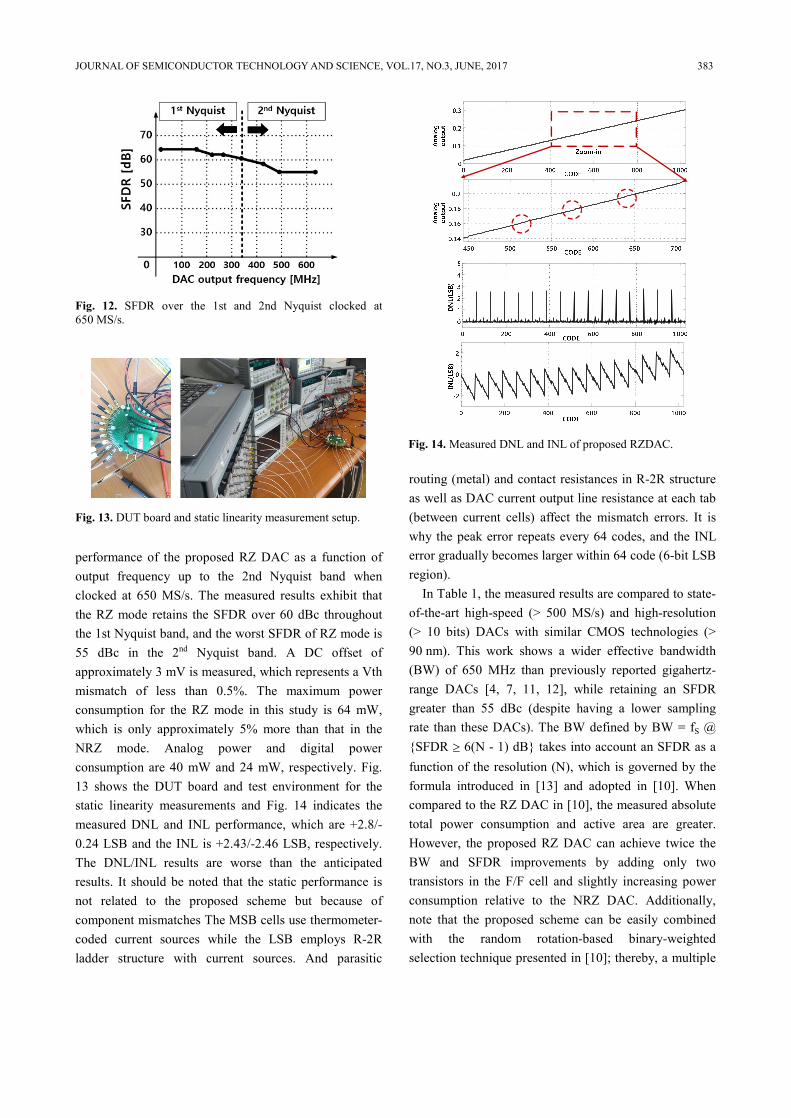
performance of the proposed RZ DAC as a function of output frequency up to the 2nd Nyquist band when clocked at 650 MS/s. The measured results exhibit that the RZ mode retains the SFDR over 60 dBc throughout the 1st Nyquist band, and the worst SFDR of RZ mode is 55 dBc in the 2nd Nyquist band. A DC offset of approximately 3 mV is measured, which represents a Vth mismatch of less than 0.5%. The maximum power consumption for the RZ mode in this study is 64 mW, which is only approximately 5% more than that in the NRZ mode. Analog power and digital power consumption are 40 mW and 24 mW, respectively. Fig. 13 shows the DUT board and test environment for the static linearity measurements and Fig. 14 indicates the measured DNL and INL performance, which are +2.8/-0.24 LSB and the INL is +2.43/-2.46 LSB, respectively. The DNL/INL results are worse than the anticipated results. It should be noted that the static performance is not related to the proposed scheme but because of component mismatches The MSB cells use thermometer-coded current sources while the LSB employs R-2R ladder structure with current sources. And parasitic
routing (metal) and contact resistances in R-2R structure as well as DAC current output line resistance at each tab (between current cells) affect the mismatch errors. It is why the peak error repeats every 64 codes, and the INL error gradually becomes larger within 64 code (6-bit LSB region).
In Table 1, the measured results are compared to state-of-the-art high-speed (> 500 MS/s) and high-resolution (> 10 bits) DACs with similar CMOS technologies (> 90 nm). This work shows a wider effective bandwidth (BW) of 650 MHz than previously reported gigahertz- range DACs [4, 7, 11, 12], while retaining an SFDR greater than 55 dBc (despite having a lower sampling rate than these DACs). The BW defined by BW = fS @ {SFDR ³ 6(N - 1) dB} takes into account an SFDR as a function of the resolution (N), which is governed by the formula introduced in [13] and adopted in [10]. When compared to the RZ DAC in [10], the measured absolute total power consumption and active area are greater. However, the proposed RZ DAC can achieve twice the BW and SFDR improvements by adding only two transistors in the F/F cell and slightly increasing power consumption relative to the NRZ DAC. Additionally, note that the proposed scheme can be easily combined with the random rotation-based binary-weighted selection technique presented in [10]; thereby, a multiple
Fig. 12. SFDR over the 1st and 2nd Nyquist clocked at 650 MS/s.
Fig. 13. DUT board and static linearity measurement setup.
Fig. 14. Measured DNL and INL of proposed RZDAC.

384 JAECHEOL YUN et al : A RETURN-TO-ZERO DAC WITH TRI-STATE SWITCHING SCHEME FOR MULTIPLE NYQUIST …
Nyquist operation and improved dynamic and static performance can be achieved.
V. CONCLUSIONS
An RZ DAC operating at a multiple-Nyquist-frequency band is presented. The proposed RZ DAC with a tri-state switch scheme provides a wideband and high-dynamic range analog output with a minimal increase in power consumption and hardware complexity. The SFDR of the proposed RZ DAC remains higher than 60 dBc throughout the 1st Nyquist band, and the worst SFDR of 55 dBc is achieved in the 2nd Nyquist band.
ACKNOWLEDGMENTS
This work was supported by the IT R&D program of MOTIE/KEIT. [10054819, Development of modular wearable platform technology for the disaster and industrial site]. It was also partially supported by the Chung-Ang University Excellent Student Scholarship in 2015.
REFERENCES
[1] A. R. Bugeja, et al, “A 14-b, 100-MS/s CMOS DAC Designed for Spectral Performance,” Solid-
States, IEEE Journal of, Vol. 34, No. 2, pp. 1719-1732, Feb., 1999.
[2] Q. Huang, et al, “A 200MS/s 14b 97mW DAC in 0.18um CMOS,” Solid-State Circuits Conference, 2004. ISSCC 2004. Digest of Technical Papers. IEEE International, pp. 364-365, Feb., 2004.
[3] B. Schafferer, et al, “A 3V CMOS 400mW 14b 1.4GS/s DAC for Multi-Carrier Applications,” Solid-State Circuits Conference, 2004. ISSCC 2004. Digest of Technical Papers. IEEE International, pp. 360-361, Feb., 2004.
[4] G. Engel, et al, “A 14b 3/6GHz Current-Steering RF DAC in 0.18um CMOS with 66dB ACLR at 2.9GHz,” Solid-State Circuits Conference, 2004. ISSCC 2004. Digest of Technical Papers. IEEE International, pp. 458-459, Feb., 2012.
[5] M. J. Choe, et al, “A 1.6-GS/s 12-bit Return-to-Zero GaAs RF DAC for Multiple Nyquist Operation,” Solid-States, IEEE Journal of, Vol. 40, No. 12, pp. 2456-2468, Dec., 2005.
[6] B. Jewett B, ”A 1.2GS/s 15b DAC for Precision Signal Generation,” Solid-State Circuits Conference, 2005. ISSCC 2005. Digest of Technical Papers. IEEE International, pp. 110-111, Feb., 2005.
[7] W. H. Tseng, et al, “A 12-Bit 1.25-GS/s DAC in 90nm CMOS with > 70dB SFDR up to 500MHz,” Solid-States, IEEE Journal of, Vol. 46, No. 12, pp. 2845-2856, Dec., 2011.
Table 1. Comparison of the state-of-the-art DACs
* BW = fs @ {SFDR ≥ 6(N-1) dB} ** FOM = (2N x BW)/Ptotal

JOURNAL OF SEMICONDUCTOR TECHNOLOGY AND SCIENCE, VOL.17, NO.3, JUNE, 2017 385
[8] W. H. Tseng, et al, “A CMOS 8-bit 1.6-GS/s DAC With Digital Random Return-to-Zero,” Circuits and Systems II: Express Briefs, IEEE Transactions on, Vol. 58, No. 1, pp. 1-5, Jan., 2011.
[9] A. V. D. Bosch, et al, “A 10-bit 1-GSample/s Nyquist Current-Steering CMOS D/A Converter,” Solid-States, IEEE Journal of, Vol. 36, No. 3, pp. 315-324, Mar., 2001.
[10] W. T. Lin, et al, “A Compact Dynamic-Performance-Improved Current-Steering DAC With Random Rotation-Based Binary-Weighted Selection,” Solid-States, IEEE Journal of, Vol. 47, No. 2, pp. 444-453, Feb., 2012.
[11] P. Palmers, et al, “A 10-Bit 1.6-GS/s 27-mW Current-Steering D/A Converter With 550-MHz 54-dB SFDR Bandwidth,” Circuits and Systems I: Fundamental Theory and Applications, IEEE Transactions on, Vol. 57, No. 11, pp. 2870-2879, Nov., 2010.
[12] X. Li, et al, “A 14 bit 500 MS/s CMOS DAC Using Complementary Switched Current Sources and Time-Relaxed Interleaving DRRZ,” Circuits and Systems I: Fundamental Theory and Applications, IEEE Transactions on, Vol. 61, No. 8, pp. 2337-2347, Aug., 2014.
[13] A. V. D. Bosch, et al, Analog Circuit Design: Scalable Analog Circuit Design, High-Speed D/A Converters, RF Power Amplifiers, MA: Kluwer, 2002, pp. 189-201.
Jaecheol Yun received the B.S. and M.S. degrees at School of Electrical and Electronics Engineering from Inha University, Incheon Korea in 1995 and Korea University, Seoul Korea in 2003, respectively, where he is currently working toward the
Ph.D. degree in electrical and electronics engineering. His research interests include ultra low power consumption and low noise ADCs for mobile camera sensor applications.
Yun-Hwan Jung received the B.S degree in electrical and electronics engineering from Chung-Ang Univer- sity, Seoul, Korea, in 2008, where he was also received the Master-Ph.D unified degree in electrical and electronics engineering in 2013.
Since 2013 he has worked for Image Development Team, System LSI Business, Samsung Electronics. His research interests include high-resolution and high-speed digital-to-analog/analog-to-digital converters for high-perfor- mance image sensor design and display driver design. He is also interested in a high-speed digital-to-analog converter design for wide-band applications.
Taegeun Yoo received the B.S., M.S., and Ph. D. degrees in electrical and electronics engineering from Chung-Ang university, Seoul, Korea, in 2009, 2011, and 2015 respectively. From 2015 to 2016, he was also with the Chung-Ang University as a
Research Professor. In 2016, he joined the Nanyang Technological University, Singapore, as a Research Fellow. His research interests include low-power data converters and high-efficiency power management ICs. He received encouragement award and silver award at the Human-Tech Paper Award hosted by Samsung Electronics in 2011 and 2014, respectively. He also received the Silkroad Award at the IEEE International Solid State Circuits Conference (ISSCC) in 2014.
Yohan Hong received the B.S. and M.S. degrees in electrical and electronics engineering from Chung-Ang University, Seoul, Korea, in 2010 and 2014, respectively, and is currently working toward the Ph.D. degree in electrical and electronics
engineering at Chung-Ang University. Since 2010, he has been involved with the development of the high-speed SerDes circuits with pre-emphasis and equalizer for Giga-bit passive optical network systems. Currently, his research interests include maximum power point tracking algorithm for a distributed PV system, pipeline ADC, and front-end system including LNA and SAR-ADC.

386 JAECHEOL YUN et al : A RETURN-TO-ZERO DAC WITH TRI-STATE SWITCHING SCHEME FOR MULTIPLE NYQUIST …
Ju Eon Kim received the B.S. and M.S. degrees at School of Electrical and Electronics Engineering from Chung-Ang University (CAU), Seoul, Korea, in 2012 and 2014, respec- tively. He is currently working toward the Ph.D. degree in electrical
and electronics engineering at CAU. His research interests include low-voltage low-power successive approximation register (SAR)-type and high-speed high-resolution hybrid-type analog-to-digital converters (ADC). He is also interested in high-performance image sensor and display driver integrated-circuit designs.
Dong-Hyun Yoon received the B.S. and M.S. degrees at School of Electrical and Electronics Engineering from Chung-Ang University (CAU), Seoul, Korea, in 2014 and 2016, respectively. He is currently working toward the Ph.D. degree in electrical
and electronics engineering at CAU. His research interests include high-resolution high-speed digital-to-analog converters (DAC) and direct digital frequency synthesizers (DDS). He is also interested in low-noise phase-locked loop (PLL), high-performance clock-and-data recovery (CDR), and ultra high-speed serializer/deserializer (SerDes) circuits.
Sung-Min Lee received the B.S. degrees at School of Electrical and Electronics Engineering from Chung-Ang University (CAU), Seoul, Korea, in 2015, where he is currently working toward the M.S. degree in electrical and electronics engineering.
His research interests include ultra low-power SAR ADCs for bio-medical applications.
Youngkwon Jo received the B.S. and Ph.D. in electronics engineering from Korea University, Korea, in 2003 and 2009, respectively. From 2009 to 2015, he was with Samsung Electronics, Hwasung, Korea, where he worked on the design of DRAM
I/O circuits. In 2016, he joined the School of Electrical and Electronics Engineering from Chung-Ang University
(CAU), Seoul, Korea, where he is research assistant professor. His research interests include high-speed links circuits and systems.
Yong Sin Kim received the B.S. and M.S. degrees in electronics from Korea University, Seoul, Korea, in 1999 and 2003, respectively, and the Ph.D. degree in electrical engi- neering from the University of California at Santa Cruz, Santa Cruz,
CA, USA, in 2008. From 2008 to 2012, he was with the University of California Advanced Solar Technologies Institute (UC Solar), where he was involved in research on optimizing power in distributed photovoltaic systems. From 2012 to 2014, he was with School of Electrical and Electronics Engineering, Chung-Ang University, Seoul, Korea, where he was involved in development of sensors for human–machine interface. Since March 2014, he has been with the School of Electrical Engineering, Korea University. His current research interests include cross-disciplinary integration of circuits and systems for energy harvesting and sensor applications.
Kwang-Hyun Baek received the B.S. and M.S. degrees from Korea University, Seoul, Korea, in 1990 and 1998, respectively. He received the Ph.D. degree in electrical engineering from the University of Illinois at Urbana-Champaign (UIUC),
IL, USA, in 2002. From 2000 to 2006, he was with the Department of High-Speed Mixed-Signal ICs as a senior scientist at Rockwell Scientific Company, formerly Rockwell Science Center (RSC), Thousand Oaks, CA, USA. At RSC, he was involved in development of high-speed data converters (ADC/DAC) and direct digital frequency synthesizers (DDFS). He was also with Samsung Electronics from 1990 to 1996. Since 2006 he has been with the School of Electrical and Electronics Engineering, Chung-Ang University (CAU), Seoul, Korea, where he is a faculty member. His research interests include high-performance analog and digital circuits such as low-power ADCs, high-speed DACs, hybrid frequency synthesizers (PLLs, DDFSs), high-speed interface circuits (CDRs, SerDes), PMIC, and near threshold-voltage (NTV) circuits.