a novel transmission line characterisation based on measurement...
TRANSCRIPT
This article was downloaded by: [Hanyang University]On: 04 June 2013, At: 11:09Publisher: Taylor & FrancisInforma Ltd Registered in England and Wales Registered Number: 1072954 Registeredoffice: Mortimer House, 37-41 Mortimer Street, London W1T 3JH, UK
International Journal of ElectronicsPublication details, including instructions for authors andsubscription information:http://www.tandfonline.com/loi/tetn20
A novel transmission linecharacterisation based onmeasurement data reconfirmationDongchul Kim a , Hyewon Kim a & Yungseon Eo aa Department of Electrical and Computer Engineering , HanyangUniversity , Ansan , KoreaPublished online: 29 Apr 2013.
To cite this article: Dongchul Kim , Hyewon Kim & Yungseon Eo (2013): A novel transmission linecharacterisation based on measurement data reconfirmation, International Journal of Electronics,DOI:10.1080/00207217.2013.785032
To link to this article: http://dx.doi.org/10.1080/00207217.2013.785032
PLEASE SCROLL DOWN FOR ARTICLE
Full terms and conditions of use: http://www.tandfonline.com/page/terms-and-conditions
This article may be used for research, teaching, and private study purposes. Anysubstantial or systematic reproduction, redistribution, reselling, loan, sub-licensing,systematic supply, or distribution in any form to anyone is expressly forbidden.
The publisher does not give any warranty express or implied or make any representationthat the contents will be complete or accurate or up to date. The accuracy of anyinstructions, formulae, and drug doses should be independently verified with primarysources. The publisher shall not be liable for any loss, actions, claims, proceedings,demand, or costs or damages whatsoever or howsoever caused arising directly orindirectly in connection with or arising out of the use of this material.

A novel transmission line characterisation based on measurementdata reconfirmation
Dongchul Kim, Hyewon Kim and Yungseon Eo*
Department of Electrical and Computer Engineering, Hanyang University, Ansan, Korea
(Received 27 August 2012; final version received 3 February 2013)
Due to inherent resonance effects and frequency-variant dielectric properties, it is verydifficult to experimentally determine the stable and accurate circuit model parametersof thin film transmission line structures over a broad frequency band. In this article, anew, simple and straightforward frequency-variant transmission line circuit modelparameter determination method is presented. Experimental test patterns for high-frequency transmission line characterisations are designed and fabricated using apackage process. The S-parameters for the test patterns are measured using a vectornetwork analyzer (VNA) from 100 MHz to 26.5 GHz. The parasitic effects dueto contact pads are de-embedded. The frequency-variant complex permittivity andresonance-effect-free transmission line parameters (i.e., the propagation constant andcharacteristic impedance) are then determined in a broad frequency band.
Keywords: transmission line; S-parameters; interconnect; complex permittivity;RLGC
1. Introduction
Wireless/optical communication systems and imaging/sensing application systems requiremillimetre (mm) wave operating frequencies and ultra-high-speed digital signals with datarates exceeding several tens of giga bits per second (Gb/s) that propagate on long (severaltens of centimetre of long lossy line) thin-film transmission lines. In the mm wavefrequency, the system may not follow conventional theory (i.e., skin effect and dielectricloss) and may not guide pure transverse electromagnetic (TEM) mode. On the contrary,for a much higher level of integration, the line pitch (i.e., the width and spacing) of thinfilm transmission lines becomes much tighter (less than several tens of μm or less). Insuch fine lines, process variations (e.g., line pitch variation due to the etching process,unclear metal roughness effects and dielectric thickness variation due to the build-upprocess) may have significant effects on the signal transients, including dispersion, signalcoupling (i.e., x-talk) and reflection. Furthermore, the interconnect lines are composed ofmetal stacks and dielectrics that are mixed with inhomogeneous materials. Althoughmanufacturers provide the respective dielectric layer material parameters (e.g., the fixeddielectric constant and loss tangent) that are based on bulk materials, these parametersmay not be accurate in such a mixed dielectric structure. Moreover, dielectric materialparameters are frequency variant (Djordjević, Biljić, Likar-Smiljanić, & Sarkar, 2001). Asa result, system designs using nominal layout dimensions and frequency-invariant mate-rial parameters may result in risky designs or fatal design errors (Hall et al., 2007; Kim &Eo, 2008). Practical problems, including non-ideal and unexpected effects (e.g., metal
*Corresponding author. Email: [email protected]
International Journal of Electronics, 2013http://dx.doi.org/10.1080/00207217.2013.785032
© 2013 Taylor & Francis
Dow
nloa
ded
by [
Han
yang
Uni
vers
ity]
at 1
1:09
04
June
201
3

roughness, process variation and mixed material dissipation factors, etc.), are foundthrough experiments. Thus, careful experimental characterisations are indispensable tocircuit designers for understanding the real performance of a device under test (DUT),thereby verifying its model and improving its design. Otherwise, the risk of failure of highperformance circuit/system design increases dramatically.
Transmission lines can be accurately characterised by two important characteristicparameters (i.e., the propagation constant and characteristic impedance). From the experi-mental point of view, the high-frequency characteristics of a DUT can be investigatedusing network parameters based on waves, not on voltages or currents. Thus, the S-parameter measurements of test transmission lines above several tens of GHz are con-sidered crucial for high-frequency characterisations. However, in practice, such thin filmtransmission line characterisation requires wafer-level characterisation, which needs tocope with many difficulties during the measurement and data processing. The difficultiesin characterising such thin film transmission lines are due to measurement reference planediscontinuities, parasitic effects de-embedding, frequency-variant dielectric properties andnon-ideal process variations. Resonances due to them may be one of the crucial problems.Even though many techniques have been developed to deal with these problems (Chen,Zhu, & Melde 2005; Kim & Han, 2003; Mangan, Voinigescu, Yang, & Tazlauanu, 2006;Nishikawa, Shintani, & Yamakawa, 2006; Tiemeijer, Pijper, & van der Heijden, van Noort,2009, 2011; van Wijnen, Claessen, & Wolsheimer, 1987), thin film transmission linecharacterisation over a broad frequency band is still very challenging. Eo and Eisenstadtproposed a transmission line characterisation method based on S-parameters (Eisenstadt &Eo, 1992; Eo & Eisenstadt, 1993). The technique is simple and straightforward. However, ithas an inaccuracy problem near the resonance frequencies (Williams & Marks, 1993;Williams, Arz, & Grabinski, 1998). The low dielectric loss approximation techniqueassumes negligible substrate loss and constant capacitance over the whole frequencyrange (Kasten, Steer, & Pomerleau, 1990; Marks & Williams, 1991). Its application islimited to the non-lossy substrate. Alternatively, for lossy substrate, the transmission lineparameters can be determined by extracting data-fitted capacitance and loss tangent (Torres-Torres, 2011) or by employing a rational function that is fitted with the data inthe frequencies that are less than a quarter wavelength (λ=4) (Kim, Oh, & Kim, 2010).In order to remove the effects due to the measurement reference plane discontinuities,Post (2005) used a linear regression technique. In contrast, Torres-Torres (2008) performedit by using a physics-based mathematical analysis technique. The resonance-effect-freetransmission line parameters can be determined using the complicated two-tier calibrationcomparison method (Williams, Marks, & Davidson, 1991). However, the technique is notstraightforward and requires a complicated data processing using an extra wafer-levelcalibration. In summary, all of them have pros and cons to be exploited in low cost, finepitch and thin film transmission line characterisations.
We propose a new, accurate and straightforward thin film transmission line character-isation technique that can avoid complicated physical interpretation and data processingduring characterisation. The technique is based on the following key ideas: (1) Thepropagation constant can be accurately and readily determined from the multi-line method(Marks, 1991); (2) Although the characteristic impedance is very sensitive to the reso-nance effects, it is very accurately determined up to the first resonance frequency usingthe ‘Eo and Eisenstadt method’ (Eisenstadt & Eo, 1992; Eo & Eisenstadt, 1993); (3) Theresonance frequency is inversely proportional to the length of a transmission line; and (4)
2 D. Kim et al.
Dow
nloa
ded
by [
Han
yang
Uni
vers
ity]
at 1
1:09
04
June
201
3

The frequency-variant complex permittivity can be accurately determined over the broadfrequency band by combining the measured propagation constant with Debye dielectricpermittivity model which satisfies the causality condition (Djordjević et al., 2001).
2. Experimental parameter determination
In order to experimentally characterise transmission lines, experimental test patterns weredesigned and fabricated using a package process. Test patterns with various line lengths (L3:3.2 mm, L5: 5.6 mm, L6: 6.5 mm and L19: 19.7 mm) were fabricated on the same test substrate,as shown in Figure 1. The S-parameters for the test patterns are measured from 100 MHz to26.5 GHz using a vector network analyzer (VNA: HP8510C) that is connected with on-waferprobe tips (Cascade Microtech ACP40-m-GSG-150). The VNA is calibrated by employing theshort-open-load-thru (SOLT) calibration method up to the probe tip. Pad dimensions are (100μm� 100 μm), and calibration reference impedance is assumed as ZREF ¼ 50Ω. Once the S-parameters are determined, the transmission line parameters can be readily extracted using the‘Eo and Eisenstadt method’ as follows (Eisenstadt & Eo, 1992):
e�γ, ¼ 1� S112 þ S212
2S21�
ffiffiffiffiffiffiffiffiffiffiffiffiffiffiffiffiffiffiffiffiffiffiffiffiffiffiffiffiffiffiffiffiffiffiffiffiffiffiffiffiffiffiffiffiffiffiffiffiffiffiffiffiffiffiffiffiðS112 � S212 þ 1Þ2 � ð2S11Þ2
ð2S21Þ2s" #�1
(1)
ZCð Þ2¼ ZREF2 ð1þ S11Þ2 � S212
ð1� S11Þ2 � S212(2)
where γ, ZC and ZREF are the propagation constant, characteristic impedance and mea-surement reference impedance, respectively.
2.1. De-embedding
We tested two de-embedding methods: (1) ABCD-parameter-based analysis technique(Kim & Han, 2003); and (2) Y-parameter-based swapping technique (Mangan et al.,
(a)
(b)
26.17 25.33
35.55
19.60
50.48
12.36
Signal
Solder Resist
FR4
Unit (μm)
Ground
Figure 1. Test transmission lines. (a) top view of the test patterns. (b) cross-sectional dimension.
International Journal of Electronics 3
Dow
nloa
ded
by [
Han
yang
Uni
vers
ity]
at 1
1:09
04
June
201
3

2006). Assuming the pad as a lumped admittance (YP), the transmission lines for twodifferent line lengths (l2 > l1), including the pad parasitics, can be represented usingABCD network parameters
1 0
YP 1
� �cosh γl1ð Þ ZC sinh γl1ð Þ
sinh γl1ð Þ=ZC cosh γl1ð Þ� �
1 0
YP 1
� �¼ A B
C D
� �l1
(3)
1 0
YP 1
� �cosh γl2ð Þ ZC sinh γl2ð Þsinh γl2ð ÞZC cosh γl2ð Þ� �
1 0
YP 1
� �¼ A B
C D
� �l2
: (4)
Combining Equations (3) and (4), the parasitic pad effects can be readily de-embedded asfollows (Kim & Han, 2003):
cosh γ l2 � l1ð Þð Þ ZC sinh γ l2 � l1ð Þð Þsinh γ l2 � l1ð Þð Þ=ZC cosh γ l2 � l1ð Þð Þ� �
¼ 1 0
�YP 1
� �M11 M12
M21 M22
� �1 0
YP 1
� �(5)
where
YP ¼ M22 �M11
2M12and
M11 M12
M21 M22
� �¼ A B
C D
� �l2
A BC D
� ��1
l1
:
Alternatively, the pad parasitics can be de-embedded using the Y-parameter-based swap-ping technique (Mangan et al., 2006),
Yde-embed;Yl2�l1 þ Swap Yl2�l1ð Þ
2;
where SwapY11 Y12
Y21 Y22
" # !;
Y22 Y21
Y12 Y11
" # ! (6)
Yl2�l1;Y � parameter ofA BC D
� �l2
A BC D
� ��1
l1
!:
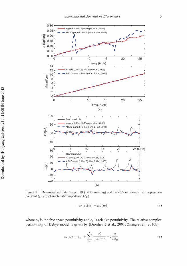
The transmission line characteristic impedances and propagation constant using thede-embedded S-parameter data are compared in Figure 2. Although the two techniquesprovide very similar accuracy, we employed the Y-parameter-based swapping techniquewhich seems to be more stable in many tests.
2.2. Complex permittivity determination
We determined the complex permittivity using Debye model which satisfies the causalitycondition. The frequency-variant complex permittivity of a dielectric material is represented by
"ðωÞ ¼ "0"rðωÞ (7)
4 D. Kim et al.
Dow
nloa
ded
by [
Han
yang
Uni
vers
ity]
at 1
1:09
04
June
201
3
¼ "0ð"0rðωÞ � j"00r ðωÞÞ (8)
where "0 is the free space permittivity and "r is relative permittivity. The relative complexpermittivity of Debye model is given by (Djordjević et al., 2001; Zhang et al., 2010b)
"rðωÞ ¼ "1 þXni¼1
"0i1þ jωτi
� jσ
ω"0(9)
(a)
0.30
0.25
0.20
0.15
0.10
0.05
0.00
14
12
10
8
6
4
2
0
0
0 5 10 15 20 25
α (N
p/c
m)
β (r
ad/c
m)
Y–para.(L19–L6) (Mangan et al., 2006)
Y–para.(L19–L6) (Mangan et al., 2006)
ABCD–para.(L19–L6) (Kim & Han, 2003)
ABCD–para.(L19–L6) (Kim & Han, 2003)
Freq. (GHz)
5 10 15 20 25
Freq. (GHz)
(b)
100
80
60
40
30
20
–20
10
–10
0
Y–para.(L19–L6) (Mangan et al., 2006)
Y–para.(L19–L6) (Mangan et al., 2006)
ABCD–para.(L19–L6) (Kim & Han, 2003)
ABCD–para.(L19–L6) (Kim & Han, 2003)
Raw data(L19)
Raw data(L19)
0 5 10 15 20 25 (GHz)
Re[Z
o]
Im[Z
o]
Figure 2. De-embedded data using L19 (19.7 mm-long) and L6 (6.5 mm-long). (a) propagationconstant (γ). (b) characteristic impedance (ZC).
International Journal of Electronics 5
Dow
nloa
ded
by [
Han
yang
Uni
vers
ity]
at 1
1:09
04
June
201
3

where "1 is real part of the relative permittivity at high frequencies, "0i is variation of thereal part of relative permittivity, τi is relaxation time constant, σ is dielectric conductivityand "0 is free space permittivity.
In an m-layered mixed structure, the effective permittivity ("r eff ) can be representedby (Mazur 1995)
"r eff ¼Xmi¼1
vi"i;Xmi¼1
vi ¼ 1 (10)
where "i is the i-th material permittivity and vi is the volume fraction of the i-th material.Since the phase constant (β) of a dielectric material is concerned with the dielectricconstant (Hayt & Buck, 2001),
β ¼ ω
ffiffiffiffiffiffiffiffiffiffiffiffiffiffiffiffiffiffiffiffiffiffiffiffiμ0"0μr"0rðωÞ
2
r ffiffiffiffiffiffiffiffiffiffiffiffiffiffiffiffiffiffiffiffiffiffiffiffiffiffiffiffiffi1þ "00r ðωÞ
"0rðωÞ� �2
sþ 1
0@
1A
1=2
(11)
the complex permittivity can be determined by combining Genetic algorithm (Davis, 1991;Zhang et al. 2010b) with the phase constant that can be readily determined from the measuredpropagation constant. The fitness function (Δ) of the Genetic algorithm is defined as
Δ ¼ 1
N
ffiffiffiffiffiffiffiffiffiffiffiffiffiffiffiffiffiffiffiffiffiffiffiffiffiffiffiffiffiffiffiffiffiffiXNi¼1
βm � βej jmax βmj j
� �2vuut (12)
where N is the number of total data points. The βm and βe are the measured phase constantand the evaluated phase constant, respectively. The complex permittivity extracted usingEquations (9)–(12) is shown in Figure 3. The one-term Debye model parameters using the
4.0
3.8
3.6
3.4
3.2
3.00 5 10 15 20 25
0.00
0.01
0.02
0.03
0.04
0.05
0.06
0.07
0.08
Real part
of
perm
ittivity
Freq. (GHz)
ε′ (real part of permittivity)
tanδ
tanδ
Figure 3. The real part of the extracted permittivity and loss tangent.
6 D. Kim et al.
Dow
nloa
ded
by [
Han
yang
Uni
vers
ity]
at 1
1:09
04
June
201
3

Genetic algorithm are as follows: "1 = 3.6082, Δ"0 = 0.1653, τ1 = 10.6130 ps andσ = 0.98340 mS/m. It is noteworthy that both the "0rðωÞ and tan δ are frequency-variant.
2.3. Transmission line circuit model parameter determination
After de-embedding, once the propagation constant and characteristic impedance aredetermined using (1) and (2), the frequency-variant transmission line circuit modelparameters can be determined as follows:
RðωÞ ¼ Re γ � Zcð Þ; LðωÞ ¼ Im γ � Zcð Þ=ω (13)
GðωÞ ¼ Re γ=Zcð Þ; CðωÞ ¼ Im γ=Zcð Þ=ω (14)
However, the transmission line circuit model parameters using (13) and (14) are stableonly until the first resonance frequency occurs. In order to solve the problem, two-tierTRL calibration comparison method is proposed (Williams, Marks, & Davidson, 1991).The technique performs the first calibration using the test patterns that are fabricated on alossless substrate. In the first calibration, neglecting conductance Gð f Þ, the characteristicimpedance of transmission lines is determined. The DUT characteristic impedance isdetermined by comparing the first calibration with the second calibration. Thereby,frequency-variant transmission line parameters can be stably determined. However, notonly does the technique require extra test patterns that are fabricated on a losslesssubstrate for the first calibration, but also the somewhat complicated calibration compar-ison has to be performed. In this work, a new straightforward frequency-variant transmis-sion line parameter determination technique is presented. The technique does not requireextra test patterns.
The frequency-variant transmission line parameters can be represented by (Zhanget al., 2010a)
Rðf Þ ¼ R0 þffiffiffif
p� RS (15)
Lðf Þ ¼ L1 þ RS=2πffiffiffif
p(16)
Cðf Þ ¼ Kg"0r"0 (17)
Gðf Þ ¼ G0 þ 2πfKg"00r "0 ¼ G0 þ ωCðf Þ tan δ (18)
where R0, RS , L1, G0 and Kg are DC (i.e., low-frequency) resistance, skin effectresistance, high-frequency inductance, DC (i.e., low-frequency) conductance and geometry-related constant, respectively. Thus, if these low-frequency parameters and frequency-variantcomplex permittivity are determined, the accurate and stable transmission line parameters canbe determined in the whole measurement frequency band.
The resonances occur whenever the line length of DUT is equal to the positive integermultiple of a half wave length (l ¼ n � λ=2). The resonance frequency can be approxi-mately estimated by
fresonance ¼ clight � n=ffiffiffiffi"0r
p � 2l� �(19)
International Journal of Electronics 7
Dow
nloa
ded
by [
Han
yang
Uni
vers
ity]
at 1
1:09
04
June
201
3

where clight , l and n are the speed of light, a line length and a positive integer, respectively.Thus, if a line length is suitably chosen, the stable transmission line parameters can bedetermined using (1), (2), (13) and (14) up to certain frequency (i.e., f � fλ=4). In otherwords, the R0, RS , L1, G0 and Kg can be readily determined with ‘Eo and Eiesenstadtmethod’, while the complex permittivity can be determined as discussed in previoussection. Combining all these parameters with (15)–(18), the frequency-variant transmis-sion line parameters can be determined in the whole measurement frequency band asshown in Figures 4–7.
Clearly, the resistance increases due to skin effect as the frequency increases. The skineffect and proximity effect reduce the total amount of the interlinked magnetic flux. Thus,the inductance decreases a bit as frequency increases and then converges to a constantvalue. The variation of the capacitance with the frequency is due to a frequency-variantdielectric permittivity which is a very little function of frequency. Unlike the capacitance,the conductance linearly increases with the frequency at low-frequency region but its slopis slacked a bit in high-frequency region.
3. Verification
The propagation constant, which can be accurately and stably extracted in the wholemeasurement frequency band, can be represented with the per-unit-length (PUL) transmis-sion line circuit model parameters:
γ ¼ffiffiffiffiffiffiffiffiffiffiffiffiffiffiffiffiffiffiffiffiffiffiffiffiffiffiffiffiffiffiffiffiffiffiffiffiffiffiffiffiffiRþ jωLð Þ Gþ jωCð Þ
p¼ αþ jβ (20)
where the loss term α is an attenuation constant and the phase delay term β is a phaseconstant. As shown in Figure 8, the attenuation constant and phase constant using the
50
40
30
20
10
00.1 1 10
Resis
tance (
Ω/c
m)
Freq. (GHz)
L19–L3
L19–L5
L19–L6
This work
Figure 4. Resistance variation with frequency.
8 D. Kim et al.
Dow
nloa
ded
by [
Han
yang
Uni
vers
ity]
at 1
1:09
04
June
201
3

extracted parameters show good agreement with the measured data. Unlike the propaga-tion constant, it is very difficult to extract the accurate and stable characteristic impedanceover a broad frequency band. The characteristic impedance can also be represented by theproposed frequency-variant PUL transmission line circuit model parameters:
10
8
6
4
2
00 5 10 15 20 25
Condu
cta
nce (
mS
/cm
)
Freq. (GHz)
L19–L3
L19–L5
L19–L6
This work
Figure 6. Conductance variation with frequency.
6.0
5.5
5.0
4.5
4.0
3.5
3.0
2.5
2.00 5 10 15
Freq. (GHz)
20 25
Inducta
nce (
nH
/cm
)
L19–L3
L19–L5
L19–L6
This work
Figure 5. Inductance variation with frequency.
International Journal of Electronics 9
Dow
nloa
ded
by [
Han
yang
Uni
vers
ity]
at 1
1:09
04
June
201
3

ZC ¼ffiffiffiffiffiffiffiffiffiffiffiffiffiffiffiffiffiffiRþ jωLGþ jωC
s¼ Re ZCð Þ þ j � Im ZCð Þ (21)
0.30
0.25
0.20
0.15
0.10
0.05
0.00
14
12
10
8
6
4
2
0
α (N
p/c
m)
β (r
ad/c
m)
0 5 10 15 20 25
Freq. (GHz)
0 5 10 15 20 25
Freq. (GHz)
L19–L3
L19–L5
L19–L6
This work
L19–L3
L19–L5
L19–L6
This work
Figure 8. Reconstructed propagation constant.
1.4
1.3
1.2
1.1
1.0
0.9
0.8
0.7
0.60 5 10
Freq. (GHz)
15 20 25
Ca
pacitance (
pF
/cm
)
L19–L3
L19–L5
L19–L6
This work
Figure 7. Capacitance variation with frequency.
10 D. Kim et al.
Dow
nloa
ded
by [
Han
yang
Uni
vers
ity]
at 1
1:09
04
June
201
3

where
Re ZCð Þ ¼ Zoffiffiffi2
p � 1þ RG=ω2LCð Þ1þ G2=ω2C2ð Þ þ
ffiffiffiffiffiffiffiffiffiffiffiffiffiffiffiffiffiffiffiffiffiffiffiffiffiffiffiffiffiffiffi1þ R2=ω2L2ð Þ1þ G2=ω2C2ð Þ
s" #1=2(22)
Im ZCð Þ ¼ Zoffiffiffi2
p � � 1þ RG=ω2LCð Þ1þ G2=ω2C2ð Þ
� �þ
ffiffiffiffiffiffiffiffiffiffiffiffiffiffiffiffiffiffiffiffiffiffiffiffiffiffiffiffiffiffiffi1þ R2=ω2L2ð Þ1þ G2=ω2C2ð Þ
s" #1=2(23)
where Zo ¼ffiffiffiffiffiffiffiffiffiL=C
p. The characteristic impedance that is free from the resonance effects is
also determined (see Figure 9). Note that the characteristic impedance abruptly changesat low frequencies, but converges to a constant value as the frequency increases. Itis noteworthy that unlike the conventionally extracted characteristic impedance, theproposed-technique-based one is reasonably well matched with the theoretical predictionexpressions of Equations (22) and (23). For the reference, the reconstructed S-parametersusing the extracted transmission line parameters are compared with the originally mea-sured S-parameters that are de-embedded as shown in Figure 10.
4. Conclusion
In this article, an accurate and straightforward high-frequency transmission line character-isation method was presented. In this method, the resonance-effect-free frequency-varianttransmission line parameters (i.e., the propagation constant and characteristic impedance)were determined using multi-line S-parameter measurement data. For the transmissionline parameter determinations, experimental test patterns were designed and fabricatedusing a packaging process. The S-parameters of the test patterns were measured using aVNA from 100 MHz to 26.5 GHz. Pad parasitics were de-embedded using well-known
90
80
70
60
50
40
20
10
–10
–20
0
0 5 10 15 20 25 (GHz)
Re
al[Z
o]
Imag[Z
o]
L19–L3
L19–L3
L19–L5
L19–L5
L19–L6
L19–L6
This work
This work
Figure 9. Reconstructed characteristic impedance.
International Journal of Electronics 11
Dow
nloa
ded
by [
Han
yang
Uni
vers
ity]
at 1
1:09
04
June
201
3

de-embedding techniques. For a mixed material, the frequency-variant complex permit-tivity was extracted by combining the measured propagation constant and Debye modelwhich satisfies the causality condition. Then combining ‘Eo and Eisenstadt method’ withDebye complex permittivity model, stable and accurate frequency-variant transmissionline circuit model parameters are determined in a broad frequency range. Since thistechnique is very simple and straightforward, it may be usefully exploited for high-frequency transmission line characterisation and/or signal integrity verification for ahigh-speed integrated system design in industry.
AcknowledgementsThis work was supported by the project, Development of Technologies for Next-generationElectromagnetic Wave Measurement Standards, of the Korea Research Institute of Standards andScience under Grant 12011016.
ReferencesChen, G., Zhu, L., & Melde, K. L. (2005). Extraction of frequency dependent RLCG parameters of
the packaging interconnects on low-loss substrates from frequency domain measurements. 14thelectrical performance of electronic packaging and systems, 25–28, Austin, TX.
Davis, L. (1991). Handbook of genetic algorithms. New York, NY: Van Nostrand Reinhold.Djordjević, A. R., Biljić, R. M., Likar-Smiljanić, V. D., & Sarkar, T. K. (2001). Wideband
frequency-domain characterization of FR-4 and time-domain causality. IEEE Transactions onElectromagnetic Compatibility, 43, 662–667.
Eisenstadt, W. R., & Eo, Y. (1992). S-parameter-based IC interconnect transmission line characterization.IEEE Transactions on Components, Hybrids, and Manufacturing Technology, 15, 483–490.
Eo, Y., & Eisenstadt, W. R. (1993). High-speed VLSI interconnect modeling based on S-parametermeasurements. IEEE Transactions on Components, Hybrids, and Manufacturing Technology,16, 555–562.
–10 1.5
1.0
0.5
–0.5
–1.0
–1.5
4
3
2
1
0
–1
–2
–3
–4
0.0
–0.5
–1.0
–1.5
–2.0
–2.5
–3.0
0.0
–15
–20
–25
–30
–35
–40
S1
1 (
dB
)S
21 (
dB
)
S1
1 (
rad
)S
21 (
rad)
0 5 10Freq. (GHz)
15 20 25
0 5 10
Freq. (GHz)
15 20 25 0 5 10
Freq. (GHz)
15 20 25
0 5 10
Freq. (GHz)
15 20 25
L19–L6
L19–L6
This work
This work
Figure 10. Reconstructed S-parameters.
12 D. Kim et al.
Dow
nloa
ded
by [
Han
yang
Uni
vers
ity]
at 1
1:09
04
June
201
3

Hall, S., Pytel, S. G., Huray, P. G., Hua, D., Moonshiram, A., Brist, G. A., & Sijercic, E. (2007).Multigigahertz causal transmission line modeling methodology using a 3-D hemisphericalsurface roughness approach. IEEE Transactions on Microwave Theory and Techniques, 55,2614–2624.
Hayt, W. H., & Buck, J. A. (2001). Engineering electromagnetics (6th ed.). New York, NY:McGraw-Hill.
Kasten, J. S., Steer, M. B., & Pomerleau, R. (1990). Enhanced through-reflect-line characterizationof two-port measuring systems using free-space capacitance calculation. IEEE Transactions onMicrowave Theory and Techniques, 38, 215–217.
Kim, H., & Eo, Y. (2008). High-frequency-measurement-based circuit modeling and power/groundintegrity evaluation of integrated circuit packages. IEEE Transaction on Advanced Packaging,31, 910–918.
Kim, J., & Han, D. (2003). Hybrid method for frequency-dependent lossy coupled transmission linecharacterization and modeling. 12th electrical performance of electronic packaging and sys-tems, 239–242, Princeton, NJ.
Kim, J., Oh, D., & Kim, W. (2010). Accurate characterization of broadband multiconductortransmission lines for high-speed digital systems. IEEE Transaction on Advanced Packaging,33, 857–867.
Mangan, A. M., Voinigescu, S. P., Yang, M., & Tazlauanu, M. (2006). De-embedding transmissionline measurements for accurate modeling of IC designs. IEEE Transaction on Electron Devices,53, 235–241.
Marks, R. B. (1991). A multiline method of network analyzer calibration. IEEE Transactions onMicrowave Theory and Techniques, 39, 1205–1215.
Marks, R. B., & Williams, D. F. (1991). Characteristic impedance determination using propagationconstant measurement. IEEE Microwave and Guided Wave Letters, 1, 141–143.
Mazur, K. (1995). Polymer-ferroelectric ceramic composites. Plastics Engineering, 28, 539–610.Nishikawa, K., Shintani, K., & Yamakawa, S. (2006). Characteristics of transmission lines fabri-
cated by CMOS process with deep n-well implantation. IEEE Transactions on MicrowaveTheory and Techniques, 54, 589–598.
Post, J. E. (2005). On determining the characteristic impedance of low-loss transmission lines.Microwave and Optical Technology Letters, 47, 176–180.
Tiemeijer, L. F., Pijper, R. M. T., & van der Heijden, E. (2011). Two multiport de-embeddingmethods for accurate on-wafer characterisation of 60-GHz differential amplifiers. IEEETransactions on Microwave Theory and Techniques, 59, 763–771.
Tiemeijer, L. F., Pijper, R. M. T., & van Noort, W. (2009). On the accuracy of the parametersextracted from S-parameter measurements taken on differential IC transmission lines. IEEETransactions on Microwave Theory and Techniques, 57, 1581–1588.
Torres-Torres, R., Romo, G., Armenta, L., & Horine., B. (2008). Analytical characteristic impedancedetermination method for microstrip lines fabricated on printed circuit boards. InternationalJournal of RF and Microwave Computer-Aided Engineering, 19, 60–68.
Torres-Torres, R. (2001). Extracting characteristic impedance in low-loss substrates, ElectronicsLetters, 47, 191–193.
van Wijnen, P. J., Claessen, H. R., & Wolsheimer, E. A. (1987). A new straight-forward calibrationand correction procedure for “on wafer” high frequency S-parameter measurements (45 MHz-18 GHz). Bipolar circuits and technology meeting, 70–73, Minneapolis, MN.
Williams, D. F., Arz, U., & Grabinski, H. (1998). Accurate characteristic impedance measurementon silicon. IEEE MTT-S symposium digest, 1917–1920, Baltimore, MD.
Williams, D. F., & Marks, R. B. (1993). Accurate transmission line characterization. IEEEMicrowave and Guided Wave Letters, 3, 247–249.
Williams, D. F., Marks, R. B., & Davidson, A. (1991). Comparison of on-wafer calibrations. 38thARFTG conference digest, 68–81, San Diego, CA.
Zhang, J., Drewniak, J. L., Pommerenke, D. J., Koledintseva, M. Y., DuBroff, R. E., Cheng, W.,Yang, Z., Chen, Q. B., & Orlandi, A. (2010a). Causal RLGC(f) models for transmission linesfrom measured S-parameters. IEEE Transaction on Electromagnetic Compatibility, 52,189–198.
Zhang, J., Koledintseva, M. Y., Antonini, G., Drewniak, J. L., Orlandi, A., & Rozanov, K. N.(2010b). Planar transmission line method for characterization of printed circuit board dielectrics.Progress In Electromagnetics Research (PIER), 102, 267–286.
International Journal of Electronics 13
Dow
nloa
ded
by [
Han
yang
Uni
vers
ity]
at 1
1:09
04
June
201
3