a novel productivity-driven logic element for field...
TRANSCRIPT
This article was downloaded by: [Bibliotheek TU Delft]On: 29 July 2013, At: 02:19Publisher: Taylor & FrancisInforma Ltd Registered in England and Wales Registered Number: 1072954 Registeredoffice: Mortimer House, 37-41 Mortimer Street, London W1T 3JH, UK
International Journal of ElectronicsPublication details, including instructions for authors andsubscription information:http://www.tandfonline.com/loi/tetn20
A novel productivity-driven logicelement for field-programmabledevicesThomas Marconi a , Koen Bertels b & Georgi Gaydadjiev ba School of Computing , National University of Singapore ,Singapore , Singaporeb Computer Engineering Lab , Delft University of Technology ,Delft , The NetherlandsPublished online: 09 Jul 2013.
To cite this article: International Journal of Electronics (2013): A novel productivity-drivenlogic element for field-programmable devices, International Journal of Electronics, DOI:10.1080/00207217.2013.794489
To link to this article: http://dx.doi.org/10.1080/00207217.2013.794489
PLEASE SCROLL DOWN FOR ARTICLE
Taylor & Francis makes every effort to ensure the accuracy of all the information (the“Content”) contained in the publications on our platform. However, Taylor & Francis,our agents, and our licensors make no representations or warranties whatsoever as tothe accuracy, completeness, or suitability for any purpose of the Content. Any opinionsand views expressed in this publication are the opinions and views of the authors,and are not the views of or endorsed by Taylor & Francis. The accuracy of the Contentshould not be relied upon and should be independently verified with primary sourcesof information. Taylor and Francis shall not be liable for any losses, actions, claims,proceedings, demands, costs, expenses, damages, and other liabilities whatsoever orhowsoever caused arising directly or indirectly in connection with, in relation to or arisingout of the use of the Content.
This article may be used for research, teaching, and private study purposes. Anysubstantial or systematic reproduction, redistribution, reselling, loan, sub-licensing,systematic supply, or distribution in any form to anyone is expressly forbidden. Terms &Conditions of access and use can be found at http://www.tandfonline.com/page/terms-and-conditions

A novel productivity-driven logic element for field-programmabledevices
Thomas Marconia*, Koen Bertelsb and Georgi Gaydadjievb
aSchool of Computing, National University of Singapore, Singapore, Singapore; bComputerEngineering Lab, Delft University of Technology, Delft, The Netherlands
(Received 13 August 2012; final version received 3 February 2013)
Although various techniques have been proposed for power reduction in field-programmable devices (FPDs), they are still all based on conventional logic elements(LEs). In the conventional LE, the output of the combinational logic (e.g. the look-uptable (LUT) in many field-programmable gate arrays (FPGAs)) is connected to theinput of the storage element; while the D flip-flop (DFF) is always clocked even whennot necessary. Such unnecessary transitions waste power. To address this problem, wepropose a novel productivity-driven LE with reduced number of transitions. Thedifferences between our LE and the conventional LE are in the FFs-type used andthe internal LE organisation. In our LEs, DFFs have been replaced by T flip-flops withthe T input permanently connected to logic value 1. Instead of connecting the output ofthe combinational logic to the FF input, we use it as the FF clock. The proposed LEhas been validated via Simulation Program with Integrated Circuit Emphasis (SPICE)simulations for a 45-nm Complementary Metal–Oxide–Semiconductor (CMOS) tech-nology as well as via a real Computer-Aided Design (CAD) tools on a real FPGAusing the standard Microelectronic Center of North Carolina (MCNC) benchmarkcircuits. The experimental results show that FPDs using our proposal not only have48% lower total power but also run 17% faster than conventional FPDs on average.
Keywords: logic element; reconfigurable devices; low power; field-programmabledevices; reconfigurable computing; architecture
1. Introduction
Field-programmable devices (FPDs) are integrated circuits that can be (re)configured bytheir end users to implement various digital functions (Brown, Brown, & Rose, 1996).There are three main categories FPD: simple of programmable logic devices (SPLDs),complex PLDs (CPLDs) and field-programmable gate arrays (FPGAs) (Brown et al. 1996).Advantages of using FPDs in run-time reconfigurable systems are instant manufacturingturnaround, reduced start-up costs, low financial risk, short time-to-market and easy designchanges (Brown et al. 1996). However to get these benefits, the users need to pay additionalcosts: higher power consumption (approximately 12× larger dynamic power), larger siliconareas (40× more area required) and lower operating speeds (3.2× slower), as compared tothe Application-Specific Integrated Circuits (ASICs) (Kuon & Rose, 2006). Higher powerconsumption requires expensive packaging (Boemo, Rivera, López-Buedo, & Meneses,1995; Gayasen, Lee, et al., 2004; Mondal & Memik, 2005b; shortens chip lifetimes (Boemoet al., 1995), asks for costly cooling systems (Boemo et al., 1995; Gayasen, Lee, et al.,2004; Mondal & Memik, 2005b), decreases system reliability (Mondal & Memik 2005b)
*Corresponding author. Email: [email protected]
International Journal of Electronics, 2013http://dx.doi.org/10.1080/00207217.2013.794489
© 2013 Taylor & Francis
Dow
nloa
ded
by [
Bib
lioth
eek
TU
Del
ft]
at 0
2:19
29
July
201
3

and prohibits battery operations (Boemo et al., 1995; Gayasen, Lee, et al., 2004; Mondal &Memik, 2005b). Therefore, reducing the power consumption of FPDs is a critical issue.
Many techniques have been proposed for lowering the power consumed by FPDs.However, all existing power reduction techniques target what we call a “conventionallogic element”. This conventional logic element (LE) has been used by researchers ofFPDs since it was patented by Birkaner and Chua in 1978 (Birkner and Chua, 1978).Although FPDs have been improved significantly since the original proposal, they stillmake use of a proposal dated 1978 that may need to be reconsidered. The conventionalLE contains the combinational logic (e.g. the look-up table (LUT) in FPGAs) and thestorage element (D flip-flop (DFF)). The output of the combinational logic is connected tothe input of the storage element; the clock input of DFF is connected to the clock signal.Since the DFF clock input is connected directly to the clock signal, the DFF is alwaysclocked even when this is not needed, i.e. unproductive activities. For example, whenD ¼ Q, the DFF does not need to be clocked. Such unnecessary transitions waste powerin FPDs using the conventional LEs. This is related to the fact that even low-power flip-flops (FFs) consume power during logic transition from zero-to-zero and from one-to-oneas shown in Lang, Musoll, and Cortadella (1997), Nogawa and Ohtomo (1998),Markovic, Nikolic, and Brodersen (2001), Zhao, Darwish, and Bayoumi (2002, 2004),Sayed and Al-Asaad (2006), and Teh et al. (2006). It is well known that the dynamicpower consumption of a CMOS circuit is proportional to its clock frequency f, loadcapacitance C, activity factor α and the square of supply voltage V 2
DD. In the case that α iszero, many researchers (e.g. Lang et al., 1997; Markovic et al., 2001; Nogawa & Ohtomo,1998; Sayed & Al-Asaad, 2006; Teh et al., 2006; Zhao, et al., 2002, 2004) have reportedthat a certain amount of dynamic power is still consumed by sequential circuits becausethe clock signal is continuously supplied. To model this phenomenon, Lang et al. (1997)define the average dynamic energy per cycle of a FF as
E ¼ Ec � Nc þ E0 � N0 þ E1 � N1 þ Egb � Ngb þ Ega � Nga;
where Ec is the energy consumed by one event during clock edges and during the realtransition of the output Q when the FF changes, E0 is the energy consumed by one eventwhen flip-flop remains in state 0 (no transition in Q), E1 is the energy consumed by oneevent when flip-flop remains in state 1 (no transition in Q), Egb is the energy consumed byone event of glitch of Q before the leading edge of the clock, Ega is the energy consumedby one event of glitch of Q after the leading edge of the clock and Nx is the correspondingaverage number of events per cycle. Lang et al. (1997) also demonstrated that a significantfraction of the energy is consumed when the FF output Q does not change. To solve thisproblem, we propose a novel productivity-driven LE for reduced FPDs power consump-tion. The proposed LE can be used in any kind of FPDs, such as SPLDs, CPLDs as wellas FPGAs. The differences between our LE and the conventional proposal are in the FF-type and the LE internal organisation. Instead of using DFFs, we use T flip-flops (TFFs)with T input permanently at logic 1 (T = 1). This is related to the fact that designingsequential circuits using TFFs is more power efficient than DFFs as reported in Wu andPedram (2001). The output of the combinational logic in our case is connected to theclock input of the FF. As a result, our LE is able to block unnecessary clock transitionswithout using additional clock gating logic, avoiding unproductive activities.
The Microelectronic Center of North Carolina (MCNC) benchmark circuits (Yang,1991) are used to evaluate our proposal in 45-nm BSIM4 CMOS technology (Cao et al.,2010). We use LTSPICE tools shown in Technology (2008) for transistor-level circuit
2 T. Marconi et al.
Dow
nloa
ded
by [
Bib
lioth
eek
TU
Del
ft]
at 0
2:19
29
July
201
3

simulations with nominal supply voltage VDD of 1.2 V. The evaluation is performed interms of total power, logic power, clock power, interconnect power, dynamic power, staticpower, speed and LE area. Moreover, to complete the evaluation, we also evaluate ourproposal using a real Computer-Aided Design (CAD) tool (Quartus II Compiler Tool,Altera Corporation, San Jose, CA) and a real FPGA from Altera by forcing the existingtool to implement circuits behaving like our proposed LE. In our previous conferencepaper Marconi, Theodoropoulos, Bertels, and Gaydadjiev (2010a), we only presentedHardware Description Language (HDL) coding style to reduce power consumption forFPGAs, no hardware architecture modification was performed. In this article, inspired byMarconi et al. (2010a), we move forward by presenting a new LE architecture for power-efficient FPDs.
The main contributions of this article are as follows:
(1) a novel productivity-driven LE for FPDs;(2) an extensive evaluation using both transistor-level circuit simulations and a real
FPGA and CAD tool experiments; and(3) reduction of total power by 48% and improvement of performance by 17%
compared to conventional FPDs on average.
The rest of the article is organised as follows. In Section 2, we review existing work indealing with power consumption issue of FPDs. Our proposed LE to tackle powerinefficiency of FPDs is presented in Section 3. In Section 4, we evaluate the proposal.Finally, we conclude in Section 5.
2. Related work
Before presenting our proposal of how to address power inefficiency in FPDs, in thissection, we present existing published work in their attempts to address the sameproblems.
One of the ways to reduce dynamic power consumption in FPDs is to stop selectedsignals from flowing or propagating to the other part of the circuits, referred as stopping-signal-to-flow technique. Clock gating, one instance of this technique, is used to reducedynamic power consumption by selectively blocking the circuit local clock when no stateor output transition takes place. The clock gating controller is needed for detecting theconditions of the observed circuit. Based on these conditions, the clock gating controllercan know the exact time when it can stop clock signal to be transported to the specificcircuit for power saving. It is used in FPGAs as reported in Cadenas and Megson (2003),Sutter, Todorovich, and Boemo (2004), Zhang, Roivainen, and Mämmelä (2006), Khan(2006), Parlak and Hamzaoglu (2007), Achronix (2008), Huda, Mallick, and Anderson(2009), Wang, Gupta, and Anderson (2009), Klein (2009), Actel (2009), Rivoallon(2010), Saleem and Khan (2010), Sterpone, Carro, Matos, Wong, and Fakhar (2011),Hussein, Klein, and Hart (2012), Ravindra and Anuradha (2012) and CPLDs as presentedin Semiconductor (2009). This technique is supported by commercial CAD tools fromXilinx (San Jose, CA) as reported in Rivoallon (2010). In Achronix (2008), an asynchro-nous FPGA with clock gating is proposed. Another example of this technique is theguarded evaluation. The idea is to stop some signals in a digital circuit that do not affectan output of the circuit for certain conditions as applied to FPGAs reported by Howlandand Tessier (2008), Anderson and Ravishankar (2010). Similar to this technique, we stopclock signals to flow to no-need-clock LEs of FPDs. At least, there are three differences
International Journal of Electronics 3
Dow
nloa
ded
by [
Bib
lioth
eek
TU
Del
ft]
at 0
2:19
29
July
201
3

from the conventional technique, such as the changing of LE architecture, the granularityof controlling and the unified path. There is no architecture changing of LE in conven-tional technique, while in our proposal, we change the architecture to make it much moresuitable in order to stop unnecessary flowing of signals efficiently and easily. Differentfrom the conventional technique that needs explicit controller to control the flow ofsignals (consuming power), our proposal implicitly builds this controller inside thecircuits. Another difference from the conventional technique is the granularity of control-ling. In our proposal, the granularity is at each single LE, while in the conventional one, itis at a group of LEs. In the conventional technique, the data path, the control path and theclock are separated, while in our proposal, we unify all of these paths into a single unifiedpath.
Another technique to reduce dynamic power consumption is to change the FF.Conventional single-edge-triggered FFs respond only once per clock pulse cycle. Toreduce power consumption, a FF that can respond to both the positive and the negativeedge of the clock pulse (double-edge-triggered flip-flops) was proposed in Uuger (1981).This technique is used in Xilinx CPLDs (Xilinx 2002). Similar to this technique, we dochange the FFs. Different from this technique, in our proposal, we change the FFs-type toT flip-flops with the T input permanently connected to logic value 1, while in conven-tional one, it still uses DFFs. Moreover, in our proposal, we do change the internal LEorganisation. Instead of connecting the output of the combinational logic to the FF input,we use it as the FF clock.
Reducing interconnection is another technique to reduce power consumption in FPDs.The design that requires less interconnection consumes less static and dynamic powerconsumptions. Modern FPGAs contain embedded hardware blocks, such as multipliers,Digital Signal Processings (DSPs) and memories. It is reported in Kuon and Rose (2006),Klein (2009) that mapping designs to these blocks requires less interconnection. Buildingcircuits with bigger size LUTs needs less interconnection between LUTs. This hastriggered commercial FPGA vendors to use bigger-sized LUTs as reported in Klein(2009), Altera (2006a). Using a diagonally symmetric interconnect pattern in Virtex-5FPGAs (Xilinx Inc., San Jose, CA) can reduce the number of interconnect routing hops asreported in Douglass (2006). Consequently, the interconnect power consumption isreduced. Constraining designs to be implemented on the specific regions within theFPGA to minimise power consumed by clock networks is reported in Wang, French,Davoodi, and Agarwal (2006). The idea is to place logic closer together for minimisingthe clock network usage. In our proposal, we do not make an effort to reduce the usage ofinterconnection resources; however, we do reduce interconnection power by minimisingthe glitches flowing to the interconnect network.
Another technique to reduce dynamic power consumption in FPDs is to reduceglitches. This is related to the fact that a circuit with fewer glitches consumes less dynamicpower. Adding programmable delay circuits into configurable logic blocks of FPGAs isreported in Lamoureux, Lemieux, and Wilton (2008). The generation of glitches isavoided by aligning the arrival times of signals using the proposed programmable delaycircuits. As a consequence, the glitches are reduced. Pipelining FPGA circuits to reducethe number of levels of the circuits between registers is reported in Wilton, Shin Ang, andLuk (2004), Bard and Rafla (2008), Rollins and Wirthlin (2005). As a result, circuits tendto produce fewer glitches. Inserting negative-edge-triggered flip-flops at the outputs ofselected LUTs to block glitches for propagating further in FPGAs is demonstrated inCzajkowski and Brown (2007). Retiming can be used to reduce glitches in FPGAs(Fischer, Buchenrieder, and Nageldinger 2005). The idea is to redistribute registers
4 T. Marconi et al.
Dow
nloa
ded
by [
Bib
lioth
eek
TU
Del
ft]
at 0
2:19
29
July
201
3

along a signal path without changing the functionality of the circuit. By doing so, thelogic between registers is minimised, hence reducing glitches. A routing that can balancearrival times of the inputs of the same LUTs in FPGAs is proposed in Dinh, Chen, andWong (2009). By doing so, the glitches are reduced. In our proposal, we reduce glitchesproduced by unnecessary clockings to the FFs.
Reducing switching activity is another technique to reduce dynamic power consumptionin FPDs. Since power consumption depends linearly on the switching activity, reducing thisresults in power consumption improvement. Reordering input signals to LUTs can reducedynamic power consumption in FPGAs. By doing so, we can minimise the switchingactivity inside LUTs as reported in Alexander (1997). Choosing state encoding of FSM tominimise the bit changes during state transitions for reducing switching activity in FPGAs isreported in Sutter, Todorovich, Lpez-Buedo, and Boemo (2002b), Mengibar, Entrena,Lorenz and Sánchez-Reillo (2003). Logic synthesis in FPGAs is a process of transforminga given design (coded in schematic or HDL) into a gate-level circuit. Minimising switchingactivity during logic synthesis for FPGAs is presented in Tinmaung, Howland, and Tessier(2007). Clock scaling is an approach to reduce switching activity by adjusting operatingclock frequency dynamically. Applying this approach in FPGAs is reported in Paulsson,Hübner and Becker (2008). In our work, we reduce the switching activity by avoidingunproductive activity caused by unnecessary clockings to LEs.
Another technique to reduce power consumed by FPDs is to turn off not-neededcircuits. Power gating is a technique for reducing power consumption by temporarilyturning off circuits that are not in use. It is applied in FPGAs (Gayasen, Tsai, et al., 2004;Hassan, et al., 2005; Ishihara, Hariyama, & Kameyama, 2010; Nair, Koppa, & John,2009; Rahman, Das, Tuan, & Trimberger, 2006). This technique is used in industrialproducts, such as Atmel PLDs (Atmel, 2000), Altera CPLDs (Altera, 2006b), ActelFPGAs (Actel, 2008), QuickLogic FPGAs (QuickLogic, 2008), Xilinx FPGAs (Klein,2009), Altera FPGAs (Khan, 2007). In Ishihara (2010), an asynchronous FPGA withautonomous fine-grain power gating is proposed. How to partition a design to benefitbetter from power gating technique is reported in Hassan et al. (2005). Dividing a finitestate machine (FSM) into two smaller sub-FSM using a probabilistic criterion is reportedin Sutter et al. (2002a).The idea is to activate only one sub-FSM at a time; meanwhile, theother is disabled for power reduction. Since not all inputs of LUTs are used in real FPGAdesigns, leakage power can be reduced by shutting-off Static Random-Access Memory(SRAM) cells and transistors associated with unused LUT inputs as reported in Mondaland Memik (2005b). Resources used by hardware tasks implemented on partially recon-figurable FPGAs cannot be turned off after configuration, consuming leakage power.Therefore, hardware tasks need to be operated as soon as possible after configuration inrun-time systems using partially reconfigurable devices. This technique for leakage powerreduction in FPGAs is reported in Li, Yuh, Yang, and Chang (2007). Similar to thistechnique, we also turn off not-needed resources for power saving.
Optimising the usage of bits to represent the processed data is another technique toreduce power consumption in FPDs. The bit-widths of the internal signals of circuits canbe optimized to reduce dynamic power consumption. A circuit with shorter bit-widthsconsumes less power. This approach applied in FPGAs is reported in Gaffar, Clarke, andConstantinides (2006), Constantinides (2006). Different from this technique, while thistechnique optimise the usage of signals at data path, in our proposal, the usage of clocksignals is optimised.
A simple technique to reduce power consumptions in FPDs is to manipulate thevoltage (e.g. reducing the supply voltage or the voltage swing, increasing threshold
International Journal of Electronics 5
Dow
nloa
ded
by [
Bib
lioth
eek
TU
Del
ft]
at 0
2:19
29
July
201
3

voltage) either statically or dynamically, called here as voltage-manipulation technique.Since there is a quadratic relationship between supply voltage and dynamic power,reducing the voltage will significantly reduce the dynamic power. Moreover, a cubicrelationship between supply voltage and leakage power reduces significantly the leakagepower. Since the dynamic power consumption is linearly proportional to the voltageswing, power is reduced by minimising the voltage swing. A lower threshold voltagetransistor runs faster, but it consumes more power. By increasing this voltage intelligentlyat certain part of the circuits, the power can be reduced without suffering performancedegradation. Klein (2009), Jenkins and Ekas (2006) reported the usage of this technique inthe lowering supply voltage in marketable FPGAs. Powering FPGAs with a variablesupply voltage is reported in Chow, Tsui, Leong, Luk, and Wilton (2005). This method isreferred as dynamic voltage scaling (DVS). Powering FPGAs with two different supplyvoltages (dual-Vdd) is reported in Gayasen, Lee, et al. (2004), Mukherjee and Memik(2005), Li, Lin, et al. (2004), Lin and He (2006), Li et al. (2004a), Hu, Lin, He, and Tuan(2008). It is to use lower supply voltages on noncritical paths to reduce power, and highersupply voltages on critical paths to maintain performance. Algorithms for Vdd assignmentare presented in Lin and He (2006), Li et al. (2004a). Hu et al. (2008) combinesconcurrently this technique with retiming to better reduce power consumption inFPGAs. Using LUTs with two different operating modes (high performance and lowpower) reduces leakage power as reported in Azizi and Najm (2005). The idea is to usesome transistors for lowering supply voltage across input inverters of LUTs during low-power operation mode. Since not all LUTs need to be operated in high-performance mode,the leakage power is reduced. Choosing the best operating mode for each memory onFPGAs based on prior knowledge of its dead intervals is reported in Meng, Sherwood,and Kastner (2006) to reduce leakage power consumption. The memory can be operatedin three operating modes: active, drowsy and sleep. The sleep mode is a condition whenthe power supply is disconnected to the memory, whereas the drowsy mode is a conditionwhen the memory is connected to a lower supply voltage. The idea is to operate thememory based on its dead intervals. The memory with long/medium/short dead interval isoperated on sleep/drowsy/active mode. To reduce interconnect power, low-voltage swinginterconnects are applied for FPGAs in George, Zhang, and Rabaey (1999), Matsumotoand Masaki (2005). Because this technique degrades the performance, in George et al.(1999), the dual-edge-triggered FFs are used to handle this degradation. Applying lowswing interconnects only on non critical paths is proposed in Matsumoto and Masaki(2005) to reduce the performance degradation of this technique. Multi-threshold voltagetechnique is to use higher threshold voltage transistors on noncritical paths to reduce staticpower, and low threshold voltage transistors on critical paths to maintain performance.This technique has been applied in industrial FPGAs as reported in Klein (2009), Jenkinsand Ekas (2006). Routing switches that can operate in three different modes, such as highspeed, low power or sleep is reported in Anderson and Najm (2004). Using dual-Vdd-dual-Vt routing switches for reducing interconnect power is demonstrated in Mondal andMemik (2005a). Applying dual-vdd and power gating techniques for routing switches isproposed in Li (2004). Instead of supply voltage or swing voltage or increasing thresholdvoltage, in our proposal, we turn off not-needed resources.
Hardware sharing is another technique to reduce power consumption in FPDs. ModernFPGAs have the ability to reconfigure part of their resources without interrupting theremaining resources at run-time. Hardware sharing can be realised by utilising this partialreconfiguration feature for power consumption reduction. Power saving using thisapproach in FPGAs is reported in Patterson (2000), Park and Burleson (1998), Tessier,
6 T. Marconi et al.
Dow
nloa
ded
by [
Bib
lioth
eek
TU
Del
ft]
at 0
2:19
29
July
201
3

Swaminathan, Ramaswamy, Goeckel, and Burleson (2005), Noguera and Kennedy(2007), Klein (2009), Kao (2005), Becker, Hübner, and Ullmann (2006). While thistechnique focuses on scheduling the hardware tasks to benefit from hardware sharing,in our work, we schedule the flow of clock signals to LEs.
Another technique to reduce power consumed by FPDs is to lower circuit capacitance.A lower capacitive circuit consumes less dynamic power. One of the ways to reducecapacitance is to use a low-k dielectric material. This technique is used by commercialFPGAs as shown in Klein (2009), Jenkins and Ekas (2006). In our proposal, clock signalsonly drive the productive LEs, while the conventional ones drive all LEs at the same time.
Optimising power consumption using CAD tools is another technique to reduce powerabsorbed by FPDs. During high-level synthesis(HLS), a circuit can be implemented bycombining functional units, such as multipliers, adders, multiplexers, etc. Each functionalunit can be realised using one of the varied implementations. Each implementationrequires a certain area and runs at a specific speed with required power consumption.To reduce power consumption, we need to choose the best design for a given circuit thatcan meet the timing requirement with minimal power. HLS algorithms for minimisingpower consumption in FPGAs are reported in Wolff, Knieser, Weyer, and Papachriston(2000), Chen, Cong, and Fan (2003). Technology mapping in FPGAs is a process oftransforming a given circuit into a circuit that only consists of LUTs. The way we mapcircuits into FPGAs can affect the power consumption. The algorithms to perform thisprocess for power reduction are presented in Anderson and Najm (2002), Chen, Cong, Li,and He (2004), Wang, Liu, Lai, and Wang (2001), Farrahi and Sarrafzadeh (1994), Li,Chen, He, and Cong (2003). The main idea is to pack nodes with high switching activityinside LUTs. By doing so, we can minimise power needed to transport signals of nodesamong LUTs. To better estimate the switching activity, glitches are considered duringtechnology mapping in Cheng, Chen, and Wong (2007). Transformation by changing thefunctionalities of LUTs with re-routing (Chen, Hwang, & Liu 1997) and without re-routing (Kumthekar, Benini, Macii, & Somenzi 2000) can be used to reduce powerconsumption in FPGAs. Chen et al. (1997) performs the transformation after technologymapping by reducing switching densities of the outputs of the LUTs, whereas Kumthekaret al. (2000) transforms the design after mapping, placement and routing by consideringswitching activity and capacitance at the outputs of the LUTs. Clustering logic blocks inFPGAs can affect reduction in power consumption. Clustering reduces the usage ofinterconnect resources. As a result, it reduces interconnect power. The optimal numberof LEs per cluster for power reduction is 12 as reported in Li et al. (2003). The way wecluster a circuit into an FPGA can affect the power consumption. The clustering algo-rithms to reduce power consumption are presented in Singh and Marek-Sadowska (2002),Chen and Cong (2004). The main idea in Singh and Marek-Sadowska (2002) is tominimise intercluster connections for reducing interconnection power. Clustering forFPGAs with dual-Vdd is shown in Chen and Cong (2004). Assigning noncritical pathsto clusters with low power supply voltage is the key idea of Chen and Cong (2004).Placement algorithms to reduce power consumption in FPGAs are presented in Gupta,Anderson, Farragher, and Wang (2007), Vorwerk, et al. (2008), Lamoureux and Wilton(2007). The main idea is to add estimated dynamic power into cost function of theplacement algorithms. Dynamic power is thus reduced during placement. A placementalgorithm that takes into account the cost of using clock network resources to reducepower consumed by clock network is reported in Lamoureux and Wilton (2007). Routingalgorithms to reduce power consumption in FPGAs are reported in Gupta et al. (2007),Dinh et al. (2009). Assigning nodes with high switching activity to low-capacitance
International Journal of Electronics 7
Dow
nloa
ded
by [
Bib
lioth
eek
TU
Del
ft]
at 0
2:19
29
July
201
3
routing resources is the main idea behind the routing algorithm for reducing interconnectpower in Gupta et al. (2007). Combining power-aware technology-mapping, clustering,placement and routing algorithms to reduce FPGA power consumption is reported inLamoureux and Wilton (2003). They found that the most contribution to the powerreduction is from the clustering algorithm. In this work, the basic building block ofFPDs, which is LE, is totally different from the conventional LE used in existing CADtools. For that reason, the way to design digital circuits out of FPDs will be different. Thisneeds changing in CAD tools. In this current work, we have not yet created automaticCAD tools, we do all the design by hands.
Another technique to minimise power consumption in FPDs is to change the config-uration memory. The idea to replace SRAM memory with nonvolatile memory targetingFPGAs is presented in Actel (2008), Zhao, Belhaire, Chappert, and Mazoyer (2009),Onkaraiah et al. (2011), Koga et al. (2010). Since SRAM memory is volatile, SRAM-based FPGAs need to be reconfigured before usage. This reconfiguration consumespower. In contrast, FPGAs that use nonvolatile memory (e.g. the commercial ActelFPGA Actel (2008)) can be operated directly without reconfiguration. The leakagepower consumed by an asymmetric SRAM cell depends on its stored data. Since 87%of the configuration memory cells in FPGAs store logic 0 in the real FPGA designGayasen, Srinivasan, Vijaykrishanan, and Kandemir (2007), using asymmetric SRAMcells with low leakage at logic 0 for FPGAs to reduce leakage power consumed byreconfiguration memory is reported in Gayasen et al. (2007). The idea is to selectpolarities for logic signals (i.e. inverted or not) that can increase the number of zerosstored on the configuration memory. Since the number of zeros is increased, the numberof memory cell that operates at low leakage is increased. Thus, the leakage powerconsumed by the reconfiguration memory is reduced. To reduce power during run-timereconfiguration, configuration memory with two different types of memories (Ramo,Resano, Mozos, & Catthoor 2006) or run-time configurable memory with two differentmodes (Wang, Miranda, Papanikohou, Catthoor, & Dehaene, 2005) is proposed. One type(mode) is optimised for high-speed operation, whereas the other type(mode) is optimisedfor low-power operation. Hardware tasks implemented on FPGAs that do not requirehigh-speed reconfiguration can be reconfigured to the low power one for power savingduring reconfiguration. In our work, there is no effort to change the configurationmemory. We only change the basic LE that builds the FPDs.
Lowering leakage power is another way to reduce power consumed by FPDs. Sinceleakage power in multiplexers is dependent on their input states, selecting polarities forlogic signals (i.e. inverted or not) so that the multiplexers are operated in low-leakagestates in the majority of time can be used to reduce leakage power in FPGAs (Anderson,Najm, & Tuan 2004). To reduce more leakage power, the work in Anderson et al. (2004)is extended by Hassan et al. (2008). In Hassan et al. (2008), not only polarity isconsidered to achieve low leakage states, but also the order of input signals to LUTs ismodified to have a better leakage power reduction. It is different from Alexander (1997)that targets dynamic power, the work in Hassan et al. (2008) targets static power byreordering input signals to LUTs. Since the leakage power is state dependent (Roy,Mukhopadhyay, & Mahmoodi-Meimand, 2003), changing this state results leakagepower reduction. Using nanoelectromechanical relays for programmable routing inFPGAs is reported in Chen et al. (2010) to reduce power consumption due to its zeroleakage and low on-resistance characteristics. Although it is more power efficient than theconventional FPGA, it is not suitable for run-time reconfigurable systems due to its largemechanical switching delay. Older generation FPGAs use dual-oxide process technology:
8 T. Marconi et al.
Dow
nloa
ded
by [
Bib
lioth
eek
TU
Del
ft]
at 0
2:19
29
July
201
3

thick oxide transistors (slow transistors) for Inputs/Outputs (IOs) and thin oxide transistors(fast transistors) for core. To reduce leakage power in FPGAs, triple-oxide processtechnology is used in modern FPGAs (e.g. Virtex-4) Abusaidi and Philofsky (2008),Klein (2009). In these FPGAs, another type of transistors with medium thickness oxide isdedicated for the configuration memory and interconnect pass gates. Leakage powerreduction is not the focus of our current work. Instead, we focus on reducing dynamicpower consumption by introducing a new architecture for basic LE for FPDs.
In summary, although many techniques have been proposed for power reduction inFPDs as discussed in this section, they are all based on conventional LEs. In theconventional LE, the output of the combinational logic (e.g. the LUT in many FPGAs)is connected to the input of the storage element; while the DFF is always clocked evenwhen it is not necessary. Such unnecessary transitions waste power. To address thisproblem, we propose a novel low-power LE as presented in Section 3.
3. The proposed logic element
The purpose of LEs in FPDs is to provide the basic programmable combinational logicand storage elements used in digital systems. An LE contains a combinational logic circuitgenerator (CLCG) and a storage element as shown in Figure 1. The CLCG is used for thecombinational function, while the storage element is used for storing temporary results.
In conventional LEs, the output of CLCG is connected to the input of the storageelement as illustrated in Figure 1(a). The storage element in the conventional LE is a DFF.
Combinational logic
circuit generator
(CLCG)
D Q
Clock
OutputInputs
Combinational logic
circuit generator
(CLCG)
T Q
Clock
Output
Inputs
1
(a)
(b)
DFF
TFF
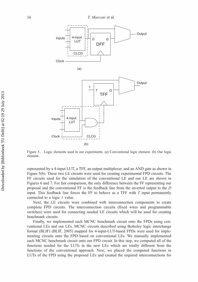
Figure 1. Logic elements. (a) Conventional logic element. (b) Our logic element.
International Journal of Electronics 9
Dow
nloa
ded
by [
Bib
lioth
eek
TU
Del
ft]
at 0
2:19
29
July
201
3

Since the clock input of DFF is connected to the clock signal, the DFF is always clocked.When the D input of DFF has a different value compared to its output Q (D � Q), theDFF needs to be clocked in order to update its state as presented in Figure 2(a).Otherwise, when D ¼ Q, the DFF does not need to be clocked. Such unnecessarytransitions (i.e. unproductive activities) will waste power in the conventional LEs.
To stop unnecessary clock transitions in conventional LEs, clock gating was introducedin previous works of Cadenas and Megson (2003), Sutter et al. (2004), Zhang et al. (2006),Khan (2006), Parlak and Hamzaoglu (2007), Achronix (2008), Huda et al. (2009), Wanget al. (2009), Klein (2009), Actel (2009), Rivoallon (2010), Saleem and Khan (2010),Sterpone et al. (2011), Hussein et al. (2012), Ravindra and Anuradha (2012) andSemiconductor (2009). In clock gating, the clock input of DFF is not anymore connecteddirectly to the clock signal, but it is controlled by the clock gating controller as shown inFigure 2(b). The clock gating controller blocks the clock signal for reaching DFFs clockinputs when the DFFs should not be clocked (D ¼ Q). As a consequence, the unnecessaryclock transitions can be avoided for power saving. The drawback of clock gating is the needof additional controllers that consume additional area and power. To reduce this overhead,the controller usually does not control an individual FF, but it controls a group of FFstogether. Hence, the clock gating cannot block all of the unnecessary clock transitions.
To solve the above issues of conventional LEs, we propose a novel low-power LEdepicted in Figure 1(b). The differences between our LE and the conventional LE are inthe type of FFs and the LE organisation. Instead of using DFFs, we use T flip-flops(TFFs) with the T input kept at logic 1. The output of the CLCG is connected to the FFclock input. No clock signal is directly connected to the TFF, the clock signal is connectedto the TFF through the CLCG when required. In FPGAs, CLCGs are implemented using
Clock
gating
controller
Clock
gating
controller
Clock
gating
controller
Clock
gating
controller
Figure 2. Basic operations of logic elements. (a) Conventional logic element without clock gating.(b) Conventional logic element with clock gating (no unnecessary clock). (c) Our logic element (nounnecessary clock).
10 T. Marconi et al.
Dow
nloa
ded
by [
Bib
lioth
eek
TU
Del
ft]
at 0
2:19
29
July
201
3

LUTs. In the case that one of the inputs of the LUT is used for feeding the clock signal,the LUT capacity is effectively decreased. In this case, our proposal needs either largerLUTs or more number of LUTs for implementing digital circuits. Since not all inputs ofLUTs are used in real FPGA designs as reported in Mondal and Memik (2005b), it ispossible that we can use these unused inputs for free to feed the clock signal. However, itis not a surprise that we need supported CAD tools to get the maximum benefits of unusedinputs. This modification of CAD tools is left as one of our future directions. In thisarticle, we only rely on the existing CAD tools, no modification of CAD tools, wasperformed.
The benefits of our LE are avoiding unnecessary clock transitions while omitting theadditional clock gating controller as shown in Figure 2(c). The CLCG avoids clocktransitions to be propagated to an individual FF when the state of the FF will not change.Thus, the unnecessary clock transitions are totally avoided at the level of individual FFsand hence dynamic power is reduced. Additional power and area are also saved incomparison to the clock gating approach, since the additional controller is not present.
Although not shown for simplicity in Figure 2, the present state and inputs are used togenerate the next state function in the conventional LE; while in our circuit, the presentstate, inputs and clock signal are used to generate the function to control TFFs clocks. Asa result, the way we design logic circuit will be different compared to the conventionalapproach. In conventional circuits, the data path, the control path and the clock areseparated. In our circuits, all these paths are combined together into a single unified path.
Allowing faster clock rates than the conventional LEs is one additional advantage of ourproposal. The FF can be clocked properly if its input is stable at least before its set-up time.In conventional LE, the input value of the DFF is not constant; it depends on the output ofthe connected CLCG. In our LE, since the T input of the TFF is constant (T ¼ 1), the TFFis always ready to be clocked. As a consequence, logic circuits implemented using our LEscan be clocked faster than logic circuits using conventional LEs.
The shortest possible clock timing diagrams for circuits using our LEs compared tothe conventional LEs are presented in Figure 3. Note that this experiment is used toinvestigate the differences in maximal clock rates. The CLCG (our) in Figure 3(b) has theclock as an additional input. This, however, does not impact the first-to-second stageshortest possible clock timing due to the tpcqðTFFÞ delay that has to be satisfied. Here,Also note that the clock signal of the first-level TFF (A) is produced by the previous-levelCLCG (our) not shown on the figure for simplicity. In the figure, tpcqðDFFÞ is the clock-to-Q propagation delay of DFF; tpdðCLCGðconvÞÞ is the propagation delay of conven-tional CLCG; tpdðCLCGðourÞÞ is the propagation delay of our CLCG; tset‐upðDFFÞ is theset-up time of DFF; tpcqðTFFÞ is the clock-to-Q propagation delay of TFF. From thisfigure, we can obtain the clock period of the circuit using conventional LEs as
TcðconvÞ � tpcqðDFFÞ þ tpdðCLCGðconvÞÞ þ tset‐upðDFFÞ (1)
and the clock period of the circuit using our LEs as
TcðOurÞ � tpcqðTFFÞ þ tpdðCLCGðOurÞÞ (2)
From Equations (1) and (2), we can obtain the speedup as
International Journal of Electronics 11
Dow
nloa
ded
by [
Bib
lioth
eek
TU
Del
ft]
at 0
2:19
29
July
201
3

SPEEDUP ¼ TcðconvÞTcðOurÞ ¼ tpcqðDFFÞ þ tpdðCLCGðconvÞÞ þ tset‐upðDFFÞ
tpcqðTFFÞ þ tpdðCLCGðourÞÞ (3)
If tpcqðDFFÞ ¼ tpcqðTFFÞ and tpdðCLCGðconvÞÞ ¼ tpdðCLCGðourÞÞ, the speedupbecomes
SPEEDUP ¼ 1þ tset‐upðDFFÞtpcqðTFFÞ þ tpdðCLCGÞ (4)
If the input of circuit changes during clock at logic 1, the possibility exists that thisinput will generate glitches that can alternate the next-stage TFF value. To address this
CLCG
(conv)
CLCG
(our)Clock
tpcq(TFF)
tset = up(DFF)
tpd(CLCG(conv))
tpcq(DFF)
tpd(CLCG(our))
D
T
Q
Q T Q
DB
B
C
A
A
A
B
B
C
C
1 1
ATc
A CTc
Q
(a)
(b)
Figure 3. Shortest clock timing of conventional (a) and our (b) logic elements.
12 T. Marconi et al.
Dow
nloa
ded
by [
Bib
lioth
eek
TU
Del
ft]
at 0
2:19
29
July
201
3

problem, we used pulsed clock signal. The width of the pulsed clock signal is set to be theminimum pulsed clock width of correctly operating TFF. In our experiments, the pulsewidth was 0.1 ns. Since the pulsed clock signal is narrow, the possibility that inputschange during clock at logic 1 is reduced. In case this very low possibility happens, thewidth of pulses caused by inputs during clock signal at logic 1 is always less than thewidth of the original pulsed clock signal and will not change the state of the TFFs. Hence,the circuit will keep working properly. It is possible to generate this narrow pulsed clocksignal as demonstrated in Kozu et al. (1996), Pontikakis and Nekili (2002), McCorkle,Huynh, and Ochoa (2006), Yuan, Zheng, Ang, and Li (2007), Paulino, Goes, and Steiger-Garcao (2008), Ardehali (2010). This option is also currently supported by state-of-the-artindustrial FPGAs (e.g. Xilinx Virtex 6) as reported in Xilinx (2012). Another way tohandle this clocking issue is to register/synchronise the input with clock signal before itgoes to the actual circuit. Since inputs are synchronised, the changing of input duringclock at logic 1 will be ignored by the circuit. However, this requires additional logic area,latency and power overhead. For that reason, we choose to use a narrow-sized pulsedclock approach in our proposal.
For exemplifying our proposal, we show here an instance of how conventional circuitsare converted into the circuits that implemented according to our proposal. Let us assumethat we have a conventional circuit as illustrated in Figure 4(a) and we want to convertthis circuit to our circuit as shown in Figure 4(b). In general, we use a simple formulawhen converting conventional circuits,
clockiðourÞ ¼ clockiðconvÞ if QiðconvÞ � DiðconvÞ0 if QiðconvÞ ¼ DiðconvÞ
�
where
clockiðourÞ is the clock input of FF i in our circuit;clockiðconvÞ is the clock input of FF i in conventional circuit;
In_0
n_n21
n_n22
In_1
In_0
n_n21
n_n22
Clock
Clock
Clock
Clock
CLCG1
(conv)
CLCG2
(conv) DFF2
DFF1
TFF1
TFF2
T Q
D Q
D QT‘1’
‘1’
Q
CLCG2
(our)
CLCG1
(our)
In_1
In_0
n_n21n_n22
In_1
In_0
n_n21
n_n11
n_n10n_n21
n_n21
Clock_n_n21
Clock_n_n22
n_n22
n_n22
n_n22
In_1
Figure 4. Simple circuit examples. (a) An example of conventional circuit. (b) An example of ourcircuit.
International Journal of Electronics 13
Dow
nloa
ded
by [
Bib
lioth
eek
TU
Del
ft]
at 0
2:19
29
July
201
3

QiðconvÞ is the Q output of FF i in conventional circuit; andDiðconvÞ is the D input of FF i in conventional circuit.
Let us assume that CLCG1ðconvÞ has the truth table as shown in Table 1. To convertCLCG1ðconvÞ to CLCG1ðourÞ, we can capture that clock1ðconvÞ ¼ clock,D1ðconvÞ ¼ n n10, Q1ðconvÞ ¼ n n21, and clock1ðourÞ ¼ clock n n21. By applying theabove formula for computing clockiðourÞ, we can obtain the truth table of CLCG1ðourÞfor the logic function of clock n n21 as shown in Table 2.
Table 1. The truth table of CLCG1ðconvÞ:In_0 In_1 n_n21 n_n22 n_n10
0 0 0 0 00 0 0 1 10 0 1 0 10 0 1 1 10 1 0 0 00 1 0 1 00 1 1 0 00 1 1 1 01 0 0 0 11 0 0 1 11 0 1 0 11 0 1 1 11 1 0 0 01 1 0 1 01 1 1 0 01 1 1 1 0
Table 2. The truth table of CLCG1ðOurÞ:In_0 In_1 n_n21 n_n22 clock_n_n21
0 0 0 0 00 0 0 1 Clock0 0 1 0 00 0 1 1 00 1 0 0 00 1 0 1 00 1 1 0 Clock0 1 1 1 Clock1 0 0 0 Clock1 0 0 1 Clock1 0 1 0 01 0 1 1 01 1 0 0 01 1 0 1 01 1 1 0 Clock1 1 1 1 Clock
14 T. Marconi et al.
Dow
nloa
ded
by [
Bib
lioth
eek
TU
Del
ft]
at 0
2:19
29
July
201
3
4. Evaluation
4.1. Transistor-level circuit evaluation
4.1.1. Experimental setup
To evaluate the proposed LE, transistor-level circuit simulations were performed usingLTSPICE tools (Technology, 2008) and 45 nm BSIM4 CMOS device models (Cao et al.,2010) with nominal VDD of 1.2 V. Because we use transistor-level simulation, all internalglitches are implicitly considered. The MCNC benchmark circuits (Yang 1991) were usedfor our study. Since our proposal is new, no CAD tools (high-level synthesis, technologymapping and place and route tools) are available for targeting FPDs using the proposedLE. For that reason, we performed all design transformations by hand. This is also whywe did not evaluate our proposal with all MCNC benchmark circuits; we only evaluatedthe proposal with the circuits that were not too complex for manual LUT design as shownin Table 3. Since our proposal saves power for circuits with storage elements, we selectedthe representative MCNC benchmark circuits.
Due to the fact that SRAM cell values remain constant after configuration (noadditional dynamic power) and there is no difference in the number of SRAM cells forFPDs using the conventional and our LEs (same static power), we do not model SRAM inour experiments. We connect the internal signals directly to VDD or ground depending onthe intended SRAM content. The simulated nMOS and pMOS transistor dimensions wereas follows: length (Ln ¼ 45 nm) / width (Wn ¼ 90 nm) and Lp ¼ 45 nm / Wp ¼ 270 nm;
respectively. The selected ratio between the nMOS and pMOS transistor widths Wp
Wn¼ 3
� �is to model the worst case scenario in respect to our proposal when leakage power isconsidered. To accurately model LUTs, multiplexers and routing circuits, we selectedtransmission-gate-based implementation as used by Xilinx commercial FPGAs patented inPi and Crotty (2003). In this experiment, we assume that unused resources can be turnedoff to model power gating both for the conventional FPDs and for our proposal. Both theconventional and our FPDs are assumed to have the same architecture parameters (e.g.segment length, connection topologies, logic block size, clock network, cluster size andLUT size). The only difference between the conventional FPDs and our FPDs is theinternal organisation of the LE.
First, we created experimental circuits representing both for the conventional and theproposed LEs. The experimental LEs are shown in Figure 5. In this experiment, anadditional AND gate for feeding clock signal was used to make manual implementationof the MCNC circuits easier. An experimental conventional LE consists of a 4-input LUT,a DFF, and an output multiplexer as illustrated in Figure 5(a); while our proposal is
Table 3. The MCNC benchmark circuits.
Names Inputs Outputs States State transitions (STs) STs to same state
bbtas 2 2 6 24 10dk27 1 2 7 14 0lion 2 1 4 11 5mc 3 5 4 10 5shiftreg 1 1 8 16 2tav 4 4 4 49 0train4 2 1 4 14 7
International Journal of Electronics 15
Dow
nloa
ded
by [
Bib
lioth
eek
TU
Del
ft]
at 0
2:19
29
July
201
3
represented by a 4-input LUT, a TFF, an output multiplexer, and an AND gate as shown inFigure 5(b). These two LE circuits were used for creating experimental FPD circuits. TheFF circuits used for the simulation of the conventional LE and our LE are shown inFigures 6 and 7. For fair comparison, the only difference between the FF representing ourproposal and the conventional FF is the feedback line from the inverted output to the Dinput. This feedback line forces the FF to behave as a TFF with T input permanentlyconnected to a logic 1 value.
Next, the LE circuits were combined with interconnection components to createcomplete FPD circuits. The interconnection circuits (fixed wires and programmableswitches) were used for connecting needed LE circuits which will be used for creatingbenchmark circuits.
Finally, we implemented each MCNC benchmark circuit onto the FPDs using con-ventional LEs and our LEs. MCNC circuits described using Berkeley logic interchangeformat (BLIF) (BLIF, 2005) mapped for 4-input-LUT-based FPDs were used for imple-menting circuits onto the FPD based on conventional LEs. We manually implementedeach MCNC benchmark circuit onto our FPD circuit. In this step, we computed all of thefunctions needed for the LUTs in the new LEs which are totally different from thefunctions of the conventional approach. Next, we placed the computed functions inLUTs of the FPD using the proposed LEs and created the required interconnections for
4-input
4-input
D Q
T Q
Figure 5. Logic elements used in our experiments. (a) Conventional logic element. (b) Our logicelement.
16 T. Marconi et al.
Dow
nloa
ded
by [
Bib
lioth
eek
TU
Del
ft]
at 0
2:19
29
July
201
3

each MCNC circuit. The reconfigurations were done by modifying the contents of the4-input LUTs, the output multiplexes, and the interconnect control signals.
We are aware that correct operation of circuits is much more important than powersavings. For that reason, before we measured the needed performance parameters, allcircuits have been verified to make sure that our circuits perform the same function as theconventional ones by using the same test vectors and the same simulation length. Figure 8shows one example of the captured waveforms during this verification. For each bench-mark circuit, we compared the simulation results of the two implementations (conven-tional and our proposal). After adopting the pulsed clock in our case, all circuits using ourLEs worked properly, functioning correctly as the conventional one. The test vectorsrepresenting all possible input values combinations were used.
Figure 7. A flip-flop circuit used in the proposed LE experiments.
Figure 6. A flip-flop circuit used in conventional LE experiments.
International Journal of Electronics 17
Dow
nloa
ded
by [
Bib
lioth
eek
TU
Del
ft]
at 0
2:19
29
July
201
3

The benchmark circuits were simulated to obtain the needed performance parameterssuch as power, speed, and area for each benchmark circuit. Area is in terms of number oftransistors required to implement the benchmark circuit using FPD circuits. The break-downs of total power which consists of logic power (total power inside LEs), clock powerand interconnect power were also obtained. To make our power study complete, we alsoanalysed the static and dynamic power. The evaluation was conducted using 500 MHzclock speed representative for the CMOS technology node assumed in our experiments.
4.1.2. Experimental results
The experimental results in terms of power consumption for FPDs using both conven-tional and proposed LEs are depicted in Tables 4 and 5. The power reduction results
(a)
(b)
1.3V
0.6V
–0.1V1.3V
–0.1V1.3V
–0.1V1.3V
–0.1V
–0.1V
0ns 40ns 80ns 120ns 160ns 200ns 240ns 280ns 320ns 360ns 400ns
0ns 40ns 80ns 120ns 160ns 200ns 240ns 280ns 320ns 360ns 400ns
1.3V
1.3V
0.6V
0.6V
0.6V
–0.1V
–0.1V
–0.1V
1.3V
1.3V
1.3V
0.7V
0.0V1.3V
0.6V
–0.1V
0.6V
0.6V
0.6V
0.6V
Figure 8. An example of correct operation experiments for shiftreg benchmark circuit usingLTSPICE tools. (a) Waveform of shifterg using conventional LEs. (b) Waveform of shifterg usingour LEs.
Table 4. Experimental results of logic, clock and interconnect power (μW).
Logic power Clock power Interconnect power
Benchmarks Conventional Our Conventional Our Conventional Our
bbtas 11357 9925 2320 811 2394 1002dk27 39105 37642 2320 891 4188 2649lion 5943 4460 1515 540 1507 627mc 28204 25913 1515 559 2282 1374shiftreg 3361 2975 2317 804 2171 777tav 40505 39480 1522 641 3886 2970train4 5576 4287 1514 538 1475 586
18 T. Marconi et al.
Dow
nloa
ded
by [
Bib
lioth
eek
TU
Del
ft]
at 0
2:19
29
July
201
3

presented in Figure 9 were computed based on the results from Tables 4 and 5. Besidespower evaluation, we also investigated the area overhead and the performance improve-ments of the FPD using the proposed LEs as shown in Figure 10.
Since the FPD using the proposed LEs avoids unnecessary clocks as discussed earlier,it consumes 63% on average less clock power compared to the FPD using conventionalLEs as shown in Figure 9. By avoiding unnecessary clocking clock inputs, the activityinside the proposed LE is also reduced. More specifically, in this case, the FPD using theproposed LEs reduces the energy denoted by Lang et al. (1997) as E0 � N0 and E1 � N1. Asa result, the FPD using proposed LEs has 12% on average less logic power compared tothe FPD using conventional LEs. This is related to the fact that even low-power FFsconsume power during logic transition from zero-to-zero and from one-to-one asdemonstrated in Lang et al. (1997), Nogawa and Ohtomo (1998), Markovic et al.(2001), Zhao et al. (2002, 2004), Sayed and Al-Asaad (2006), and Teh et al. (2006).In this work, we found that clocking a FF when its input at the condition of no making
Table 5. Experimental results of dynamic, static and total power (μW).
Dynamic power Static power Total power
Benchmarks Conventional Our Conventional Our Conventional Our
bbtas 14461 9650 1610 2088 16071 11738dk27 44166 39257 1447 1925 45613 41182lion 8047 4390 918 1237 8965 5627mc 30444 25970 1557 1876 32001 27846shiftreg 6720 2948 1129 1608 7849 4556tav 44034 40893 1879 2198 45913 43091train4 7647 4174 918 1237 8565 5411
–60
–40
–20
0
20
40
60
80
bbta
s
dk27
lion
mc
shiftr
eg
tav
train
4
Po
wer
red
uct
ion
(%
)
Logic_power Clock_power Interconnect_power
Dynamic_power Static_power Total_power
Figure 9. Power reduction (%).
International Journal of Electronics 19
Dow
nloa
ded
by [
Bib
lioth
eek
TU
Del
ft]
at 0
2:19
29
July
201
3

state changing (e.g. DFF when its input D at logic 0 while its Q is also at logic 0) willnot change the output Q of the FF (no logical transition); however, if we inspect furtherits output Q, we can see the voltage at output Q indeed changes (physical voltagechanging), consuming power. This behaviour is like the one observed by other research-ers (e.g. Lang et al., 1997; Markovic et al., 2001; Nogawa & Ohtomo, 1998; Sayed &Al-Asaad, 2006; Teh et al., 2006; Zhao et al., 2002, 2004). Since the FPD using ourproposal is clocked only if needed, this kind of activities is avoided. More precisely, inthis case, the FPD using the proposed LEs reduces the energy denoted by Lang et al.(1997) as Egb � Ngb and Ega � Nga. These glitches propagate through the interconnectresources of the FPDs, consuming power. By avoiding these glitches, the FPD using ourLEs consumes 49% on average lower interconnect power compared to the FPD usingconventional LEs.
The FPD using our proposal reduces 30% on average dynamic power compared to theFPD using conventional LEs by avoiding unnecessary activities such as clock, logic, andinterconnect as presented in Figure 9. Since the proposed experimental LE has anadditional AND gate, the FPD has 30% on average higher static power as shown inFigure 9 and 4% on average bigger area compared to the FPD using conventional LEs aspresented in Figure 10. In the future, not in this article, since not all inputs of LUTs areused in real designs as reported in Mondal and Memik (2005b), we can use these unusedinputs to feed the clock signal. In this case, we can avoid the additional logic level (theAND gate) for feeding the clock signal.
Although the FPD using our LEs consumes more static power than the FPD usingconventional elements, the overall power consumption of the FPD using our proposal islower than the conventional one as shown in Figure 9. Since the impact of increase instatic power is lower than the impact of reducing the clock, logic and interconnect powers,the FPD using our proposed LEs still can reduce 25% on average total power compared tothe FPD using conventional LEs as shown in Figure 9.
Circuits that do not change their internal state very often will avoid many clocktransitions and will be able to achieve more dynamic power reduction compared to
Figure 10. Area overhead and performance improvement (%).
20 T. Marconi et al.
Dow
nloa
ded
by [
Bib
lioth
eek
TU
Del
ft]
at 0
2:19
29
July
201
3

circuits that frequently change their states. As shown in Table 3, the state of the storageelements in the dk27 and tav benchmark circuits never remains the same. That is why thetotal power reduction achieved for these benchmark circuits is smaller compared to otherbenchmark circuits.
In the conventional LE, the DFF can be clocked by clock signal if only if the D inputis ready before the needed set-up time for the FF to work properly. In contrast, the TFF inour LE is always ready to receive clock signal because the T input of its TFF is alwaysready at logic 1. Thus, the FPD using proposed LEs runs 28% on average faster than theFPD using conventional LEs as shown in Figure 10.
4.2. Evaluation using a real CAD tool on a real FPGA
4.2.1. Experimental set-up
To evaluate our proposal further, in this experiment, we force a CAD tool to implementcircuits in the real FPGA behaving like our proposed LE using a new HDL coding style.This coding style is presented in our previous work: Marconi et al. (2010a, 2010b),Marconi (2011).
The experimental set-up is shown in Figure 11. Each MCNC benchmark circuit (Yang,1991) is converted into two Very High Speed Integrated Circuit (VHSIC) HardwareDescription Language (VHDL) files (conventional and our VHDL files) to represent thetwo VHDL coding styles (conventional and our coding styles). Each VHDL file iscompiled for Stratix EP1S10F484C5 (Altera Corporation, San Jose, CA) usingCompiler Tool from Quartus II. The area needed for implementing each circuit in termsof number of LEs is reported by the Altera Compiler Tool. The Waveform Editor from
BLIF input file (MCNC benchmark circuit)
Conventional BLIF to VHDL converter
Conventional VHDL file
Compiler Tool
Implemented conventional/our circuitConventional/our
area
Simulation ToolWaveform Editor
Timing Analyzer
Conventional/our
speed
Conventional/our
simulation result
Signal
activity file
PowerPlay Power
Analyzer Tool
Conventional/our
power consumption
Quartus II 6.0
from Altera
Verification
Our BLIF to VHDL converter
Our VHDL file
Figure 11. Experimental setup.
International Journal of Electronics 21
Dow
nloa
ded
by [
Bib
lioth
eek
TU
Del
ft]
at 0
2:19
29
July
201
3

Quartus II is used to generate test vectors for each benchmark circuit. Those vectors areapplied to the implemented circuit using Simulation Tool from Quartus II. Since thefunctional correctness is much more important than power savings, each circuit is verifiedby comparing the simulation results between the conventional and our circuits. This stepis needed to ensure that these circuits generate functionally correct identical circuits. Oneinstance of this verification is shown in Figure 12. Besides generating simulation results,the Simulation Tool also generates the signal activity file (SAF). To evaluate powerconsumption, the SAF file and the implemented circuit from the previous step are fedinto the Quartus II PowerPlay Power Analyzer Tool to obtain total, dynamic and staticpower results. To compare performance of the implemented circuits, the Timing Analyzerfrom Quartus II is used. Our study focused on the maximum clock frequency.
4.2.2. Experimental results
The experimental results of power consumption using a 50 MHz clock are presented inTable 6. Table 6 shows that our proposal can lead to reduction in dynamic power and totalpower, but will not reduce static power. Since our proposal can avoid unnecessarytransitions by clocking flip-flops only when needed, it can lead to reduction in dynamicpower consumption (75% on average) compared to conventional circuit. The degree ofpower reduction depends on the nature of the circuit, circuits with many unnecessarytransitions can take more advantages of our proposal in terms of power consumption. This75% dynamic power reduction results in only 15% on average total power consumptionreduction at 50 MHz since the static power is dominating. The static power reported bythe tools for all of the investigated circuits was 187.5 mW.
(a)
(b)
Figure 12. An example of correct operation experiments for bbara benchmark circuit usingthe simulation tool of Quartus II from Altera. (a) Waveform of bbara using conventional LEs.(b) Waveform of bbara using our LEs.
22 T. Marconi et al.
Dow
nloa
ded
by [
Bib
lioth
eek
TU
Del
ft]
at 0
2:19
29
July
201
3
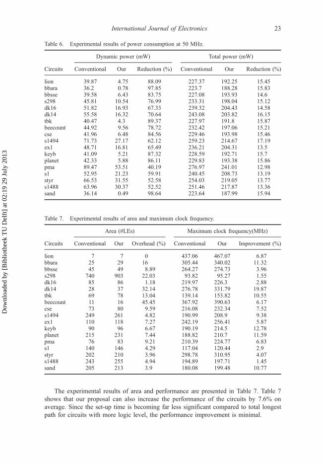
The experimental results of area and performance are presented in Table 7. Table 7shows that our proposal can also increase the performance of the circuits by 7.6% onaverage. Since the set-up time is becoming far less significant compared to total longestpath for circuits with more logic level, the performance improvement is minimal.
Table 6. Experimental results of power consumption at 50 MHz.
Dynamic power (mW) Total power (mW)
Circuits Conventional Our Reduction (%) Conventional Our Reduction (%)
lion 39.87 4.75 88.09 227.37 192.25 15.45bbara 36.2 0.78 97.85 223.7 188.28 15.83bbsse 39.58 6.43 83.75 227.08 193.93 14.6s298 45.81 10.54 76.99 233.31 198.04 15.12dk16 51.82 16.93 67.33 239.32 204.43 14.58dk14 55.58 16.32 70.64 243.08 203.82 16.15tbk 40.47 4.3 89.37 227.97 191.8 15.87beecount 44.92 9.56 78.72 232.42 197.06 15.21cse 41.96 6.48 84.56 229.46 193.98 15.46s1494 71.73 27.17 62.12 259.23 214.67 17.19ex1 48.71 16.81 65.49 236.21 204.31 13.5keyb 41.09 5.21 87.32 228.59 192.71 15.7planet 42.33 5.88 86.11 229.83 193.38 15.86pma 89.47 53.51 40.19 276.97 241.01 12.98s1 52.95 21.23 59.91 240.45 208.73 13.19styr 66.53 31.55 52.58 254.03 219.05 13.77s1488 63.96 30.37 52.52 251.46 217.87 13.36sand 36.14 0.49 98.64 223.64 187.99 15.94
Table 7. Experimental results of area and maximum clock frequency.
Area (#LEs) Maximum clock frequency(MHz)
Circuits Conventional Our Overhead (%) Conventional Our Improvement (%)
lion 7 7 0 437.06 467.07 6.87bbara 25 29 16 305.44 340.02 11.32bbsse 45 49 8.89 264.27 274.73 3.96s298 740 903 22.03 93.82 95.27 1.55dk16 85 86 1.18 219.97 226.3 2.88dk14 28 37 32.14 276.78 331.79 19.87tbk 69 78 13.04 139.14 153.82 10.55beecount 11 16 45.45 367.92 390.63 6.17cse 73 80 9.59 216.08 232.34 7.52s1494 249 261 4.82 190.99 208.9 9.38ex1 110 118 7.27 242.19 256.41 5.87keyb 90 96 6.67 190.19 214.5 12.78planet 215 231 7.44 188.82 210.7 11.59pma 76 83 9.21 210.39 224.77 6.83s1 140 146 4.29 117.04 120.44 2.9styr 202 210 3.96 298.78 310.95 4.07s1488 243 255 4.94 194.89 197.71 1.45sand 205 213 3.9 180.08 199.48 10.77
International Journal of Electronics 23
Dow
nloa
ded
by [
Bib
lioth
eek
TU
Del
ft]
at 0
2:19
29
July
201
3

The clock signal needs to be fed to LUTs before it reaches the flip-flops, ourproposal consumes 11% on average more area compared to the conventional one asshown in this table. If the clock signal can be fed to LUTs using unused inputs, our styledoes not need additional LUTs for this purpose (e.g. lion). However, if this is not thecase, our proposal will consume more LEs as shown in Table 7. In our experiment, wehad considered this area overhead when we evaluated power consumption andperformance.
To investigate all implemented circuits further, we run them using different clockfrequencies: 100, 150 and 200 MHz. The results of this experiment are presented inTable 8. Note that some of the benchmarks did not synthesised at this frequency for bothdesign styles (shown with a dash sign in the table). Since static power, area andperformance are not affected by changing the clock frequency, these tables only showdynamic power and total power consumption results. From these tables, we can observethat dynamic power consumption is linearly proportional to clock frequency. These tablesalso show that our proposal can reduce total power consumption by 25%, 32% and 36%on average compared to conventional one at 100, 150 and 200 MHz, respectively. Sincedynamic power is higher when the clock frequency is increased, the reduction of totalpower is also increased for higher clock frequencies.
Note that simple experimental circuits were used in earlier evaluation. To furtherevaluate the proposal, we experimented with bigger representative circuits by duplicatingmultiple simple circuits into the FPGA and investigated the effect on overall powerreduction as depicted in Figure 13. More working circuits means additional dynamicpower; the dynamic power becomes more dominant compared to static power. As a result,our proposal reduces more total power when the number of circuits simultaneouslyimplemented on the FPGA increases. This figure indicates that our proposal can reducetotal power by 47% on average at 50 MHz. Total power is significantly reduced at higherfrequency, at least 53% at 300 MHz for bigger circuits. Total power reduction saturates as
Table 8. Power reduction at 100, 150 and 200 MHz.
Dynamic power reduction (%) Total power reduction (%)
Circuits 100 150 200 100 150 200
lion 88.09 88.09 88.09 26.28 34.31 40.49bbara 97.85 97.85 97.85 27.26 35.89 42.64bbsse 83.75 83.75 83.75 24.86 32.47 38.34dk16 67.33 67.33 67.33 23.97 30.52 35.35dk14 70.64 70.64 70.64 26.29 33.25 38.32tbk 89.37 – – 26.95 – –beecount 78.72 78.72 78.72 25.5 32.92 38.52cse 84.56 84.56 84.56 26.14 33.97 39.94s1494 62.12 62.12 – 26.93 33.2 –ex1 65.49 65.49 65.49 22.39 28.68 33.37keyb 87.32 87.32 – 26.61 34.64 –planet 86.11 86.11 – 26.79 34.77 –pma 40.19 40.19 40.19 19.63 23.66 26.37s1 59.91 – – 21.62 – –styr 52.58 52.58 52.58 21.82 27.11 30.85s1488 52.52 52.52 – 21.3 26.56 –sand 98.64 98.64 – 27.45 36.14 –
24 T. Marconi et al.
Dow
nloa
ded
by [
Bib
lioth
eek
TU
Del
ft]
at 0
2:19
29
July
201
3

shown in Figure 13. This effect is caused by the constant static power contribution thatwill start dominating the total power number when the number of implemented circuitsincreases.
Since the closest related work is clock gating technique, we conclude this section withTable 9 that shows the comparison between our solution and clock gating solutions. Clockgating results are obtained from the original papers: Cadenas and Megson (2003), Sutteret al. (2004), Zhang et al. (2006), Parlak and Hamzaoglu (2007), Huda et al. (2009), Wanget al. (2009), Rivoallon (2010), Saleem and Khan (2010), Sterpone et al. (2011), Hussein
0
10
20
30
40
50
60
70
80
90
100
100 1 2 3 4 5 6 7 8 9 11
Number of circuits
To
tal p
ow
er r
edu
ctio
n (
%)
50 MHz
100 MHz
150 MHz
200 MHz
250 MHz
300 MHz
Figure 13. Overall power reduction (%) versus number of circuits.
Table 9. Comparison to clock gating solutions.
Proposals Power reduction Performance
Cadenas and Megson (2003) No power benefit Not availableSutter et al. (2004) 0–39% dynamic power 0–4.7 ns delay penaltyZhang et al. (2006) 5–33% total power Not availableParlak and Hamzaoglu (2007) up to 13% total power Not availableHuda et al. (2009) 6.2–7.7% total power 0–2% slowerWang et al. (2009) 1.8–27.9% total power 1.1% fasterRivoallon et al. (2010) up to 30% dynamic power Not availableSaleem and Khan (2010) 5–7.33% total power Not availableSterpone et al. (2011) 40–62% total power Not availableHussein et al. (2012) 10–80% dynamic power Not availableRavindra and Anuradha (2012) 20% total power Not availableOur 48% total power on average 17% faster on average
International Journal of Electronics 25
Dow
nloa
ded
by [
Bib
lioth
eek
TU
Del
ft]
at 0
2:19
29
July
201
3

et al. (2012), and Ravindra and Anuradha (2012). Unlike clock gating, our proposal doesnot need an additional controller to stop clock propagation. As a consequence, the FPDusing our proposed LEs not only consumes 48% less total power by avoiding unnecessaryactivities: clock, logic, and interconnect, but also it runs 17% faster than traditional FPDson average of all experimental results (i.e. SPICE simulations and real FPGA implemen-tations). Refering to the gap between FPGAs and ASICs presented in Kuon and Rose(2006), our proposal can reduce the power consumption gap from 12 times to 6 times. Wecould not directly compare the area overhead since this information is not reported in theclock gating papers considered. In our case the area overhead is 22.5% on average of theoverall experimental results.
5. Conclusions
In this article, we have proposed a novel low-power LE to replace the conventionalstructures in PLDs and FPGAs. Since unnecessary clock transitions are avoided, the clockpower is reduced. By avoiding unnecessary clock transitions, the activity inside theproposed LEs is also reduced. As a result, the FPD using the proposed LEs consumesless logic power compared to the FPD using conventional LEs. Because of activityreduction, the LEs interconnect power is also reduced compared to the FPD usingconventional LEs. Moreover, since we do not need an additional controller to holdclock activity, power and area are reduced in comparison to clock gating.
In our LE, since the T input of the FF is always in logic 1, the FF is always ready to beclocked. As a consequence, the FPD using our proposed LEs not only consumes less totalpower by avoiding unnecessary activities: clock, logic, and interconnect, but also runsfaster compared to conventional LEs because of its “always ready” flip-flops.
The proposed LE has been validated and evaluated via SPICE simulations for a 45-nmCMOS technology as well as via a real CAD tool (Altera Quartus II Compiler Tools) on areal FPGA (Altera Stratix EP1S10F484C5) using the standard MCNC benchmark circuits.The overall experimental results show that FPDs using our proposal not only have 48%lower total power but also run 17% faster than conventional FPDs on average.
Designing circuits targeting FPDs based on our proposed low-power LEs wasperformed by hand in this work. To make this design process automatically, CAD toolsdevelopment for FPDs targeting our proposed LEs is needed to be investigated further.Benefits of replacing FFs with latches are increased performace, area reduction andminimized power consumption as have been investigated in ASIC designs. Anotherinteresting research direction is to study of replacing FFs with latches in FPDs targetingour proposed LEs. Applying the proposed idea in this current work to ASICs could alsobe investigated further.
AcknowledgementsThis work is sponsored by the hArtes project (IST-035143) supported by the Sixth FrameworkProgramme of the European Community under the thematic area Embedded Systems. Besides, thefirst author has also been supported by MOE Singapore research grant No. MOE2009-T2-1-033.The authors would like to thank Prof. Jarmo Takala, Dr. Dimitris Theodoropoulos and the reviewersfor their valuable comments, suggestions and helps.
26 T. Marconi et al.
Dow
nloa
ded
by [
Bib
lioth
eek
TU
Del
ft]
at 0
2:19
29
July
201
3

ReferencesAbusaidi, P., Klein, M., & Philofsky, B. (2008). Virtex-5 FPGA system power design considera-
tions. Xilinx WP285 (v1.0).Achronix. (2008). Introduction to Achronix FPGAs. WP001 Rev.1.6.Actel. (2008). Total system power: Evaluating the power profile of FPGAs. Mountain View, CA:
Actel Corporation.Actel. (2009). Dynamic power reduction in flash FPGAs. Application Note AC323. Mountain View,
CA: Actel Corporation.Alexander, M. J. (1997). Power optimization for FPGA look-up tables. Proceedings of the 1997
international symposium on Physical design, Napa Valley, CA, ISPD ’97, pp. 156–162. NewYork, NY: ACM.
Altera. (2006a). FPGA Architecture. WP‐01003. San Jose, CA: Altera Corporation.Altera. (2006b). Power management in portable systems using MAX II CPLDs. Application Note,
422. San Jose, CA: Altera Corporation.Anderson, J., & Najm, F. (2002). Power-aware technology mapping for LUTbased FPGAs.
Proceedings of IEEE international conference on field-programmable technology, 16–18December (pp. 211–218). Washington, DC: IEEE.
Anderson, J., & Najm, F. (2004). A novel low-power FPGA routing switch. Proceedings of theIEEE custom integrated circuits conference, 3–6 October, pp. 719–722. Washington, DC: IEEE.
Anderson, J. H., Najm, F. N., & Tuan, T. (2004). Active leakage power optimization for FPGAs.Proceedings of the 2004 ACM/SIGDA 12th international symposium on Field programmablegate arrays, Monterey, CA, FPGA ’04, pp. 33–41. New York, NY: ACM.
Anderson, J. H., & Ravishankar, C. (2010). FPGA power reduction by guarded evaluation.Proceedings of the 18th annual ACM/SIGDA international symposium on Field programmablegate arrays, Monterey, CA, FPGA ’10, pp. 157–166. New York, NY: ACM.
Ardehali, M. (2010). Narrow pulse generator. US Patent No. 7782111 B2.Atmel. (2000). Saving power with Atmel PLDs. Atmel Application Note. San Jose, CA: Atmel
Corporation.Azizi, N., & Najm, F. (2005). Look-up table leakage reduction for FPGAs. Proceedings of the IEEE
custom integrated circuits conference, 21 September, pp. 187–190. Washington, DC: IEEE.Bard, S., & Rafla, N. I. (2008). Reducing power consumption in FPGAs by pipelining. Proceedings
of circuits and systems, pp. 173–176. Washington, DC: IEEE.Becker, J., Hübner, M., & Ullmann, M. (2006). Run-time FPGA reconfiguration for power-/cost-
optimized real-time systems. Proceedings of the international conference on very large scaleintegration of system-on-chip, 16–18 October. Washington, DC: IEEE.
Berkeley Logic Interchange Format (BLIF). (2005). Berkeley, CA: University of CaliforniaBerkeley.
Birkner, J. M., & Chua, H. T. (1978). Programmable Array Logic Circuit. US Patent No. 4124899.Boemo, E. I., Rivera, G. G. d., López-Buedo, S., & Meneses, J. M. (1995). Some notes on power
management on FPGA-based systems. in Proceedings of the 5th international workshop on field-programmable logic and applications, FPL ’95, London, pp. 149–157. Berlin: Springer-Verlag.
Brown, S., Brown, S., & Rose, J. (1996). Architecture of FPGAs and CPLDs: A tutorial. IEEEDesign and Test of Computers, 13, 42–57.
Cadenas, O., & Megson, G. (2003). Power performance with gated clocks of a pipelined Cordiccore. Proceedings of the 5th international conference on ASIC, 2003., October. (Vol. 2, pp.1226–1230).
Cao, Y., Balijepalli, A., Sinha, S., Wang, C. C., Wang, W., & Zhao, W. (2010). The predictivetechnology model in the late silicon era and beyond. Foundations and Trends in ElectronicDesign Automation, 3, 305–401.
Chen, C., Parsa, R., Patil, N., Chong, S., Akarvardar, K., Provine, J., …, , & Mitra, S. (2010).Efficient FPGAs using nanoelectromechanical relays. Proceedings of the 18th annual ACM/SIGDA international symposium on Field programmable gate arrays, Monterey, CA, FPGA ’10(pp. 273–282). New York, NY: ACM.
Chen, C. S., Hwang, T., & Liu, C. L. (1997). Low power FPGA design a reengineering approach.Proceedings of the 34th annual design automation conference, Anaheim, CA, DAC ’97 (pp.656–661). New York, NY: ACM.
International Journal of Electronics 27
Dow
nloa
ded
by [
Bib
lioth
eek
TU
Del
ft]
at 0
2:19
29
July
201
3

Chen, D., & Cong, J. (2004). Delay optimal low-power circuit clustering for FPGAs with dualsupply voltages. in Proceedings of the 2004 international symposium on Low power electronicsand design, Newport Beach, CA, ISLPED ’04 (pp. 70–73). New York, NY: ACM.
Chen, D., Cong, J., & Fan, Y. (2003). Low-power high-level synthesis for FPGA architectures.Proceedings of the 2003 international symposium on Low power electronics and design, Seoul,Korea, ISLPED ’03 (pp. 134–139). New York, NY: ACM.
Chen, D., Cong, J., Li, F., & He, L. (2004). Low-power technology mapping for FPGA architectureswith dual supply voltages. Proceedings of the 2004 ACM/SIGDA 12th international symposiumon Field programmable gate arrays, Monterey, CA, FPGA ’04, New York, NY, USA: ACM.
Cheng, L., Chen, D., & Wong, M. D. F. (2007). GlitchMap: an FPGA technology mapper for lowpower considering glitches. Proceedings of the 44th annual design automation conference, SanDiego, CA, DAC ’07 (pp. 318–323). New York, NY: ACM.
Chow, C. T., Tsui, L. S. M., Leong, P. H. W., Luk, W., & Wilton, S. J. E. (2005). Dynamic voltagescaling for commercial FPGAs. Proceedings of IEEE International conference on field-pro-grammable technology, pp. 173–180. Washington, DC: IEEE.
Constantinides, G. A. (2006). Word-length optimization for differentiable nonlinear systems. ACMTransactions on Design Automation of Electronic Systems, 11, 26–43.
Czajkowski, T. S., & Brown, S. D. (2007). Using negative edge triggered ffs to reduce glitchingpower in FPGA circuits. Proceedings of the 44th annual design automation conference, SanDiego, CA, DAC ’07 (pp. 324–329). New York, NY: ACM.
Dinh, Q., Chen, D., & Wong, M. D. (2009). A routing approach to reduce glitches in low powerFPGAs. Proceedings of the 2009 international symposium on physical design, San Diego, CA,ISPD ’09 (pp. 99–106). New York, NY: ACM.
Douglass, S. (2006). Introducing the Virtex-5 FPGA Family. Xilinx.Farrahi, A. H., & Sarrafzadeh, M. (1994). FPGA technology mapping for power minimization.
Proceedings of international workshop on field-programmable logic and applications: Field-programmable logic, architectures, synthesis and applications, 849, 66–77. Berlin: Springer.
Fischer, R., Buchenrieder, K., & Nageldinger, U. (2005). Reducing the power consumption ofFPGAs through retiming. Proceedings of the 12th IEEE international conference and work-shops on engineering of computer-based systems (pp. 89–94). Washington, DC: IEEE ComputerSociety.
Gaffar, A. A., Clarke, J. A., & Constantinides, G. A. (2006). PowerBit – power aware arithmeticbit-width optimization. Proceedings of IEEE international conference on field programmabletechnology, 13–15 December (pp. 289–292). Washington, DC: IEEE.
Gayasen, A., Lee, K., Vijaykrishnan, N., Kandemir, M. T., Irwin, M. J., & Tuan, T. (2004). A dual-VDD low power FPGA architecture. Proceedings of the international conference on field-programmable logic and its applications (FPL), 3203, 145–157. Berlin: Springer.
Gayasen, A., Srinivasan, S., Vijaykrishnan, N., & Kandemir, M. T. (2007). Design of power-awareFPGA fabrics. International Journal of Embedded Systems, 3(1/2). 52–64.
Gayasen, A., Tsai, Y., Vijaykrishnan, N., Kandemir, M., Irwin, M. J., & Tuan, T. (2004). Reducingleakage energy in FPGAs using region-constrained placement. Proceedings of the 2004 ACM/SIGDA 12th international symposium on field programmable gate arrays, Monterey, CA,FPGA ’04 (pp. 51–58). New York, NY: ACM.
George, V., Zhang, H., & Rabaey, J. (1999). The design of a low energy FPGA. Proceedings of the1999 international symposium on Low power electronics and design, San Diego, CA, ISLPED’99 (pp. 188–193). New York, NY: ACM.
Gupta, S., Anderson, J., Farragher, L., & Wang, Q. (2007). CAD techniques for power optimizationin virtex-5 FPGAs. Proceedings of IEEE custom integrated circuits conference, September (pp.85–88). Washington, DC: IEEE.
Hassan, H., Anis, M., Daher, A. E., & Elmasry, M. (2005). Activity packing in FPGAs for leakagepower reduction. Proceedings of the conference on design, automation and test in Europe –Volume 1, DATE ’05 (pp. 212–217). Washington, DC: IEEE Computer Society.
Hassan, H., Anis, M., & Elmasry, M. I. (2008). Input vector reordering for leakage power reductionin FPGAs. IEEE Transactions on Computer-Aided Design of Integrated Circuits and Systems,27(9). 1555–1564.
Howland, D., & Tessier, R. (2008). RTL dynamic power optimization for FPGAs. Proceedings ofIEEE midwest symposium on circuits and systems, August (pp. 714–717). Washington, DC:IEEE.
28 T. Marconi et al.
Dow
nloa
ded
by [
Bib
lioth
eek
TU
Del
ft]
at 0
2:19
29
July
201
3

Hu, Y., Lin, Y., He, L., & Tuan, T. (2008). Physical synthesis for FPGA interconnect powerreduction by dual-Vdd budgeting and retiming. ACM Transactions on Design Automation ofElectronic Systems, 13, 30: 1–30:29.
Huda, S., Mallick, M., & Anderson, J. H. (2009). Clock gating architectures for FPGA powerreduction. Proceedings of IEEE international conference on field-programmable logic andapplications (FPL) (pp. 112–118). Berlin: Springer.
Hussein, J., Klein, M., & Hart, M. (2012) Lowering power at 28 nm with Xilinx 7 series FPGAs.,Xilinx WP389.
Ishihara, S., Hariyama, M., & Kameyama, M. (2010). A low-power FPGA based on autonomousfine-grain power gating. IEEE Transactions on Very Large Scale Integration (VLSI) Systems,PP(99), 1–13.
Jenkins, C., & Ekas, P. (2006). Low-power Software-defined Radio Design using FPGAs, Altera.Kao, C. (2005). Benefits of Partial Reconfiguration, Xilinx.Khan, M. (2006). Power Optimization in FPGA Designs, Altera.Khan, M. (2007). Power Optimization Innovations in 65-nm FPGAs, Altera.Klein, M. (2009). Power Consumption at 40 and 45 nm, Xilinx WP298.Koga, M., Iida, M., Amagasaki, M., Ichida, Y., Saji, M., Iida, J., & Sueyoshi, T. (2010). First
prototype of a genuine power-gatable reconfigurable logic chip with FeRAM cells. FPL' 10 (pp.298–303).
Kozu, S., Daito, M., Sugiyama, Y., Suzuki, H., Morita, H., Nomura, M., … Yano, Y. (1996). A100 MHz, 0.4 W RISC processor with 200 MHz multiply adder, using pulse-register technique.Solid-state circuits conference, 1996. Digest of technical papers. 42nd ISSCC., 1996 IEEEInternational, February (pp. 140–141, 432).
Kumthekar, B., Benini, L., Macii, E., & Somenzi, F. (2000). Power optimization of FPGA-baseddesigns without rewiring. IEE Proceedings Computers and Digital Techniques, 147(3), 167–174.
Kuon, I., & Rose, J. (2006). Measuring the gap between FPGAs and ASICs. Proceedings of the2006 ACM/SIGDA 14th international symposium on Field programmable gate arrays,Monterey, CA, FPGA ’06 (pp. 21–30). New York, NY: ACM.
Lamoureux, J., Lemieux, G. G. F., & Wilton, S. J. E. (2008). GlitchLess: Dynamic powerminimization in FPGAs through edge alignment and glitch filtering. IEEE Transactions onVery Large Scale Integration Systems, 16, 1521–1534.
Lamoureux, J., & Wilton, S. J. E. (2003). On the interaction between power-aware FPGA CADalgorithms, Proceedings of the 2003 IEEE/ACM international conference on computer-aideddesign, ICCAD ’03 (pp. 701–708). Washington, DC: IEEE Computer Society.
Lamoureux, J., & Wilton, S. J. E. (2007). Clock-aware placement for FPGAs. Proceedings ofinternational conference on field programmable logic and applications (pp. 124–131). Berlin:Springer.
Lang, T., Musoll, E., & Cortadella, J. (1997). Individual flip-flops with gated clocks for low powerdatapaths. IEEE Transactions on Circuits and Systems II: Analog and Digital SignalProcessing, 44(6), 507–516.
Lattice Semiconductor Corporation (2009). Practical low power CPLD design. Hillsboro, OR:Lattice Semiconductor.
Li, C. F., Yuh, P. H., Yang, C. L., & Chang, Y. W. (2007). Post-placement leakage optimization forpartially dynamically reconfigurable FPGAs. Proceedings of the 2007 international symposiumon Low power electronics and design, Portland, OR, ISLPED ’07 (pp. 92–97). New York, NY:ACM.
Li, F., Chen, D., He, L., & Cong, J. (2003). Architecture evaluation for powerefficient FPGAs.Proceedings of the 2003 ACM/SIGDA eleventh international symposium on Field program-mable gate arrays, Monterey, CA, FPGA ’03 (pp. 175–184). New York, NY: ACM.
Li, F., Lin, Y., & He, L. (2004a). FPGA power reduction using configurable dual- Vdd. Proceedingsof the 41st annual design automation conference, San Diego, CA, DAC ’04 (pp. 735–740). NewYork, NY: ACM.
Li, F., Lin, Y., & He, L. (2004b). Vdd programmability to reduce FPGA interconnect power.Proceedings of the 2004 IEEE/ACM International conference on Computer-aided design,ICCAD ’04 (pp. 760–765). Washington, DC: IEEE Computer Society.
Li, F., Lin, Y., He, L., & Cong, J. (2004c). Low-power FPGA using pre-defined dual-Vdd/dual-Vtfabrics. Proceedings of the 2004 ACM/SIGDA 12th international symposium on field program-mable gate arrays, Monterey, CA, FPGA ’04 (pp. 42–50). New York, NY: ACM.
International Journal of Electronics 29
Dow
nloa
ded
by [
Bib
lioth
eek
TU
Del
ft]
at 0
2:19
29
July
201
3

Li, H., Mak, W. K., & Katkoori, S. (2003). Efficient LUT-based FPGA technology mapping forpower minimization. Proceedings of the 2003 Asia and South Pacific design automationconference, Kitakyushu, Japan, ASP-DAC ’03 (pp. 353–358). New York, NY: ACM.
Lin, Y., & He, L. (2006). Dual-Vdd interconnect with chip-level time slack allocation for FPGApower reduction. IEEE Transactions on Computer-Aided Design of Integrated Circuits andSystems, 25(10), 2023–2034.
Linear Technology (2008). SwitcherCAD III/LTspice getting started guide. Milpitas, CA: LinearTechnology.
Marconi, T., Theodoropoulos, D., Bertels, K., & Gaydadjiev, G. (2010a). A novel HDL coding styleto reduce power consumption for reconfigurable devices, Proceedings of the internationalconference on field-programmable technology (FPT) (pp. 295–299). Washington, DC: IEEE.
Marconi, T., Theodoropoulos, D., Bertels, K., & Gaydadjiev, G. (2010b). A novel HDL coding stylefor power reduction in FPGAs. Technical Report, Computer Engineering Lab CE-TR-2010-02,Delft University of Technology, Delft.
Marconi, T. (2011). Efficient runtime management of reconfigurable hardware resources, PhDThesis, Computer Engineering Lab, Delft University of Technology, Delft.
Markovic, D., Nikolic, B., & Brodersen, R. W. (2001). Analysis and design of lowenergy flip-flops.Proceedings of international symposium on low power electronics and design (pp. 52–55). NewYork, NY: ACM.
Matsumoto, Y., & Masaki, A. (2005). Low-power FPGA using partially low swing routing archi-tecture. Electronics and Communications in Japan (Part III: Fundamental Electronic Science),88(11), 11–19.
McCorkle, J. W., Huynh, P. T., & Ochoa, A., Method and apparatus for generating narrow pulsewidth monocycles. US Patent No. 7030663 B2 (2006).
Meng, Y., Sherwood, T., & Kastner, R. (2006). Leakage power reduction of embedded memories onFPGAs through location assignment. Proceedings of the 43rd annual design automation con-ference, San Francisco, CA, DAC ’06 (pp. 612–617). New York, NY: ACM.
Mengibar, L., Entrena, L., Lorenz, M. G., & S´anchez-Reillo, R. (2003). State encoding for low-power FSMs in FPGA. Proceeding of power and timing modeling, optimization and simulation(Vol. 2799, pp. 31–40). Berlin: Springer.
Mondal, S., & Memik, S. O. (2005a). A low power FPGA routing architecture, Proceedings ofinternational symposium on circuits and systems (pp. 1222–1225). Washington, DC: IEEE.
Mondal, S., & Memik, S. O. (2005b). Fine-grain leakage optimization in SRAM based FPGAs,Proceedings of the ACM great lakes symposium on VLSI (pp. 238–243). New York, NY: IEEE.
Mukherjee, R., & Memik, S. O. (2005). Evaluation of dual VDD fabrics for low power FPGAs,Proceedings of Asia and South Pacific design automation conference (pp. 1240–1243).Washington, DC: IEEE.
Nair, P., Koppa, S., & John, E. (2009, August). A comparative analysis of coarse-grain and fine-grain power gating for FPGA lookup tables, Proceedings of IEEE international midwestsymposium on circuits and systems (pp. 507–510).
Nogawa, M., & Ohtomo, Y. (1998). A data-transition look-ahead DFF circuit for statistical reductionin power consumption, IEEE Journal of Solid-State Circuits, 33(5), 702–706.
Noguera, J., & Kennedy, I. O. (2007). Power reduction in network equipment through adaptivepartial reconfiguration, Proceedings of field-programmable logic and applications (FPL) (pp.240–245). Washington, DC: IEEE.
Onkaraiah, S., Gaillardon, P. E., Reyboz, M., Clermidy, F., Portal, J. M., Bocquet, M., & Muller, C.(2011). Using OxRRAM memories for improving communications of reconfigurable FPGAarchitectures. Proceedings of the 2011 IEEE/ACM international symposium on nanoscalearchitectures, NANOARCH ’11. Washington, DC: IEEE Computer Society (pp. 65–69).
Park, S. R., & Burleson, W. (1998). Reconfiguration for power saving in real-time motion estima-tion. Proceedings of international conference on acoustics, speech, and signal processing (pp.3037–3040). Washington, DC: IEEE.
Parlak, M., & Hamzaoglu, I. (2007). A low power implementation of H.264 adaptive deblockingfilter algorithm. Proceedings of the second NASA/ESA conference on adaptive hardware andsystems, AHS ’07 (pp. 127–133). Washington, DC: IEEE Computer Society.
Patterson, C. (2000). A dynamic FPGA implementation of the Serpent Block Cipher, Proceedings ofthe second international workshop on cryptographic hardware and embedded systems, CHES’00 (pp. 141–155). London: Springer-Verlag.
30 T. Marconi et al.
Dow
nloa
ded
by [
Bib
lioth
eek
TU
Del
ft]
at 0
2:19
29
July
201
3

Paulino, N., Goes, J., & Steiger-Garcao, A. (2008, May). A CMOS variable width short-pulsegenerator circuit for UWB RADAR applications, IEEE international symposium on circuits andsystems, 2008. ISCAS 2008 (pp. 2713–2716). Washington, DC: IEEE.
Paulsson, K., Hübner, M., & Becker, J. (2008, September). Exploitation of dynamic and partialhardware reconfiguration for on-line power/performance optimization, Proceedings of reconfi-gurable communication-centric SoCs (pp. 699–700). Washington, DC: IEEE.
Pi, T., & Crotty, P. J. (2003). FPGA lookup table with transmission gate structure for reliable low-voltage operation. US Patent No. 6667635.
Pontikakis, B., & Nekili, M. (2002). A novel double edge-triggered pulse-clocked TSPC D flip-flopfor high-performance and low-power VLSI design applications, IEEE international symposiumon circuits and systems, 2002. ISCAS 2002 (Vol. 5, pp. V–101–V–104). Washington, DC: IEEE.
QuickLogic. (2008). Minimizing energy consumption with very low power mode in PolarProsolution platform CSSPs. Application Note, 88. Sunnyvale, CA: QuickLogic.
Rahman, A., Das, S.,Tuan, T., &Trimberger, S. (2006, September). Determination of powergating granularity for FPGA fabric, Proceedings of custom integrated circuits conference(pp. 9–12). Washington, DC: IEEE.
Ramo, E. P., Resano, J., Mozos, D., & Catthoor, F. (2006). A configuration memory hierarchy forfast reconfiguration with reduced energy consumption overhead. Proceedings of the 20thinternational conference on parallel and distributed processing, Rhodes Island, Greece,IPDPS’06 (pp. 189–189). Washington, DC: IEEE Computer Society.
Ravindra, J., & Anuradha, T. (2012). Article: Design of low power RISI processor by applying clockgating technique. International Journal of Applications, 43(20), 38–42, Published byFoundation of Computer Science, New York, USA.
Rivoallon, F. (2010). Reducing switching power with intelligent clock gating, Xilinx WP370 (v1.1).Rollins, N., & Wirthlin, M. J. (2005). Reducing energy in FPGA multipliers through Glitch
reduction. Proceedings of international conference on military applications of programmablelogic devices (pp. 1–10). Washington, DC: NASA.
Roy, K., Mukhopadhyay, S., & Mahmoodi-Meimand, H. (2003). Leakage current mechanisms andleakage reduction techniques in deep-submicrometer CMOS circuits, Proceedings of the IEEE,91(2), 305–327.
Saleem, A., & Khan, S. (2010, August). Low power state machine design on FPGAs. 2010 3rdinternational conference on advanced computer theory and engineering (ICACTE) (Vol. 4, pp.V4–442–V4–445). Washington, DC: IEEE.
Sayed, A., & Al-Asaad, H. (2006, August). A new low power high performance flip-flop. 49th IEEEinternational midwest symposium on circuits and systems, 2006. MWSCAS '06 (Vol. 1, pp.723–727). Washington, DC: IEEE.
Singh, A., & Marek-Sadowska, M. (2002). Efficient circuit clustering for area and power reductionin FPGAs. Proceedings of the 2002 ACM/SIGDA tenth international symposium on field-programmable gate arrays, Monterey, CA, FPGA ’02 (pp. 59–66). New York, NY: ACM.
Sterpone, L., Carro, L., Matos, D., Wong, S., & Fakhar, F. (2011). A new reconfigurable clock-gating technique for low power SRAM-based FPGAs, DATE '11 (pp. 752–757). Washington,DC: IEEE.
Sutter, G., Todorovich, E., & Boemo, E. (2004). Design of Power Aware FPGA based Systems,Proceedings of Jornadas de Computación Reconfigurable y Aplicaciones (JCRA) (pp. 1–10).
Sutter, G., Todorovich, E., Lpez-Buedo, S., & Boemo, E. I. (2002a). FSM decomposition for lowpower in FPGA, Proceedings of IEEE international conference on field-programmable logicand applications (FPL) (Vol. 2438, pp. 350–359). Washington, DC: IEEE.
Sutter, G., Todorovich, E., Lpez-Buedo, S., & Boemo, E. I. (2002b). Low-power FSMs in FPGA:Encoding alternatives. Proceeding of power and timing modeling (Vol. 2451, pp. 363–370).Berlin: Springer.
Teh, C. K., Hamada, M., Fujita, T., Hara, H., Ikumi, N., & Oowaki, Y. (2006). Conditional datamapping flip-flops for low-power and high-performance Systems. IEEE Transactions on VeryLarge Scale Integration (VLSI) Systems, 14(12), 1379–1383.
Tessier, R., Swaminathan, S., Ramaswamy, R., Goeckel, D., & Burleson, W. (2005). A reconfigur-able, power-efficient adaptive Viterbi decoder. IEEE Transactions on Very Large ScaleIntegration (VLSI) Systems, 13, 484–488.
Tinmaung, K. O., Howland, D., & Tessier, R. (2007). Power-aware FPGA logic synthesis usingbinary decision diagrams. Proceedings of the 2007 ACM/SIGDA 15th international symposium
International Journal of Electronics 31
Dow
nloa
ded
by [
Bib
lioth
eek
TU
Del
ft]
at 0
2:19
29
July
201
3

on field programmable gate arrays, Monterey, California, USA, FPGA ’07 (pp. 148–155). NewYork, NY: ACM.
Uuger, S. H. (1981). Double-edge-triggered flip-flops. IEEE Transaction on Computation, 30,447–451.
Vorwerk, K., Raman, M., Dunoyer, J., Hsu, Y., Kundu, A., & Kennings, A. A. (2008). A techniquefor minimizing power during FPGA placement. Proceedings of international conference on fieldprogrammable logic and applications (pp. 233–238). Washington, DC: IEEE.
Wang, H., Miranda, M., Papanikolaou, A., Catthoor, F., & Dehaene, W. (2005). Variable taperedpareto buffer design and implementation allowing run-time configuration for low-powerembedded SRAMs. IEEE Transactions on Very Large Scale Integration (VLSI) Systems, 13,1127–1135.
Wang, L., French, M., Davoodi, A., & Agarwal, D. (2006). FPGA dynamic power minimizationthrough placement and routing constraints, EURASIP Journal on Embedded Systems, 2006,7–7. Berlin: Springer.
Wang, Q., Gupta, S., & Anderson, J. H. (2009). Clock power reduction for virtex-5 FPGAs.Proceedings of ACM/SIGDA international conference on field programmable gate arrays(FPGA) (pp. 13–22). New York, NY: ACM.
Wang, Z. H., Liu, E. C., Lai, J., & Wang, T. C. (2001). Power minimization in LUT-based FPGAtechnology mapping. Proceedings of the Asia and South Pacific design automation conference(pp. 635–640). Washington, DC: IEEE.
Wilton, S. J. E., shin Ang, S., & Luk, W. (2004). The impact of pipelining on energy per operationin field-programmable gate arrays. Proceedings of field programmable logic and applications(pp. 719–728). Berlin: Springer-Verlag.
Wolff, F., Knieser, M., Weyer, D., & Papachristou, C. (2000). High-level low power FPGA designmethodology. Proceedings of the IEEE National aerospace and electronics conference(pp. 554–559). Washington, DC: IEEE.
Wu, X., & Pedram, M. (2001). Low-power sequential circuit design using T flip-flops. InternationalJournal of Electronics, 88, 635–643.
Xilinx. (2002). Low power design with coolrunner-II CPLDs. XAPP377.Xilinx. (2012). Virtex-6 FPGA clocking resources. UG362.Yang, S. (1991). Logic Synthesis and Optimization Benchmarks User Guide Version 3.0,
Proceedings of international workshop on logic and synthesis. Washington, DC: IEEE.Yuan, T., Zheng, Y., Ang, C. W., & Li, L. W. (2007, June). A fully integrated CMOS transmitter for
ultra-wideband applications. Radio frequency integrated circuits (RFIC) symposium, 2007 IEEE(pp. 39–42).
Zhang, Y., Roivainen, J., & Mämmelä, A. (2006). Clock-gating in FPGAs: A novel and comparativeevaluation. Proceedings of EUROMICRO conference on digital system design (pp. 584–590).Washington, DC: IEEE.
Zhao, P., Darwish, T., & Bayoumi, M. (2002, August). Low power and high speed explicit-pulsedflip-flops. The 2002 45th midwest symposium on circuits and systems, 2002. MWSCAS-2002(Vol. 2, pp. II–477–II–480).
Zhao, P., Darwish, T. K., & Bayoumi, M. A. (2004). High-performance and lowpower conditionaldischarge flip-flop. IEEE Transactions on Computer-Aided Design of Integrated Circuits andSystems, 12(5), 477–484.
Zhao, W., Belhaire, E., Chappert, C., & Mazoyer, P. (2009). Spin transfer torque (STT)-MRAM–based runtime reconfiguration FPGA circuit. ACM Transactions on Embedded ComputingSystems, 9(2), 14: 1–14:16.
32 T. Marconi et al.
Dow
nloa
ded
by [
Bib
lioth
eek
TU
Del
ft]
at 0
2:19
29
July
201
3