a novel power reduction design using approximate...
TRANSCRIPT

International Journal of Science, Engineering and Technology Research (IJSETR), Volume 3, Issue 10, October 2014
2565
ISSN: 2278 – 7798 All Rights Reserved © 2014 IJSETR
A Novel Power Reduction Design using
Approximate Adders for Inexact Computing Meera G, T.Jagannadha Swamy
Department of Electronics and Communication Engineering
Gokaraju Rangaraju Institute of Engineering & Technology, JNTUH
Abstract—Power consumption is a major issue for integrated
circuit design in nano scale CMOS technology. To reduce
power consumption, approximate implementations of a circuit
have been considered as a potential solution for applications
in which strict exactness is not required. In inexact
computing, power reduction is achieved through the
relaxation of the otherwise demanding requirement of
accuracy. Previous researches used error resiliency mainly
through voltage over scaling or using algorithmic and
architectural techniques to reduce the resulting errors. In this
paper, we propose logic complexity reduction at the transistor
level as the alternative approach to take advantage of the
relaxation of numerical accuracy. We examined this concept
by proposing several imprecise or approximate full adder cell
with reduced complexity at the transistor level, and used them
to design approximate full adders. The final approximation
consisting of nine transistors was found to consume the least
power of all. Power savings of up to 70% was achieved using
the proposed approximate adders, when compared to
previous implementations using accurate adders.
Keywords—approximate adders, mirror adder, low power
digital circuits
Introduction
Today there is an escalating number of portable
applications with limited power availability, requiring
small area, low-power and high throughput circuitry.
Therefore circuits which consume low power become the
major concern factor for design of microprocessors and system components. The research effort in low power
microelectronics has been intensified and low power VLSI
systems have emerged as exceedingly in demand.
In highly integrated nano-scale designs, reliability
issues resulting from PVT (process, voltage and
temperature) variations, aging effects and soft errors have
become major impediments for leveraging the benefits of a
lower device scaling; moreover, leakage and static power
are significant concerns for the high power consumption
encountered at such high density. A potential solution to
lower power dissipation is to employ approximate circuit designs [1]
Commonly used multimedia applications have
digital signal processing (DSP) blocks as core. Most of
these DSP blocks implement algorithms, in which the
ultimate output is either an image or a video for human
presentation and analysis. For example, the limited
perception of human vision allows the outputs of these
algorithms to be numerically approximate rather than
accurate [2]. The relaxation on numerical exactness
provides at least some freedom to perform imprecise or
approximate computation. The development of imprecise,
but simplified arithmetic units can provide an extra layer of
power saving over conventional low-power design
techniques such as using a lower supply voltage. As basic
building blocks in many digital circuits, adders have been
investigated for approximate implementations. This paper
proposes the new 9 transistor approximate adder circuit. A
reduction in logic complexity is accomplished at transistor
level by removing some of the transistors required in the accurate adder design. Additionally, the node capacitances
and thus dynamic power are reduced to lower the
power/energy consumption of the proposed circuits. In this
paper, delay, energy consumption, area and power-delay
product are measured for comparing the different designs
with an accurate adder.
A similar work appeared in [3]. We extend the paper
in [3] by giving one more simplified version of the MA.
We also introduced a methodology that can be used to
harness maximum power savings using approximate
adders, subject to a specific quality constraint. Our contributions in this paper are summarized as follows. To
simplify the logic complexity of a conventional MA cell by
reducing the number of transistors and switched
capacitances. Keeping this aim in mind, we propose five
various simplified versions of the MA, ensuring minimum
errors in the full adder (FA) truth table.
I. Conventional Full Adder
Adder is one of the most vital components of a
CPU (central processing unit), Arithmetic logic unit (ALU), and floating point unit and address generation units
like cache or memory access unit. On the other hand,
increasing demand for portable equipments such as cellular
phones, personal digital assistant (PDA), and Notebook
personal computer, arise the need of using area and Power
efficient VLSI circuits. Low-power and high-speed adder
cells are used in battery-operation based devices. Fig 1
shows the schematic of a Conventional Full Adder.

International Journal of Science, Engineering and Technology Research (IJSETR), Volume 3, Issue 10, October 2014
2566
ISSN: 2278 – 7798 All Rights Reserved © 2014 IJSETR
Fig 1: Schematic of Conventional Full Adders
Approximate Full Adders
In several approximate implementations, multiple-
bit adders are divided into two modules: the (accurate)
upper part of more significant bits and the (approximate)
lower part of less significant bits. For each lower bit, a
single-bit approximate adder implements a modified, thus
inexact function of the addition. This is often accomplished
by simplifying a full adder design at the circuit level, equivalent to a process that alters some entries in the truth
table of a full adder at the functional level.
Approximate Mirror Adders (AMAs)
A mirror adder (MA) is a common yet efficient
adder design. Five approximate Mirror Adders (AMAs)
have been obtained from a logic reduction at the transistor
level, i.e., by removing some transistors to attain a lower
power dissipation and circuit complexity. A faster
charging/discharging of the node capacitance in an AMA also incurs a shorter delay. Hence, the AMAs trade off
accuracy for energy, area and performance.
II. Strategies for the Mirror Adder
In the Strategies for Mirror Adders we describe
step-by-step procedures for coming up with various approximate MA cells with fewer transistors. Cancellation
of some series connected transistors will facilitate faster
charging and discharging of node capacitances. Moreover,
complexity reduction by removal of transistors also leads
in reducing the αC term (switched capacitance) in the
dynamic power expression Pdynamic = αCV2DDf , where
α is a switching activity or average number of switching
transitions per unit time and C is the load capacitance being
charged/discharged. This directly results in less power
dissipation. Area reduction is also accomplished by this
process. Now, let us focus on the conventional MA implementation followed by the proposed approximations.
Conventional Mirror Adders
Fig 2: Conventional Mirror Adders
Fig.2 shows the transistor-level schematic of a
conventional MA , which is a famous way of implementing
a FA. It contains a total of 24 transistors. Since this
implementation is based on complementary MOS logic, it
gives a good opportunity to design an approximate version
with removal of selected transistors.
Mirror Approximation Adder 1
Fig 3: Mirror Approximation adder 1
Fig 3 shows the approximation Mirror adder. In
order to get approximate MA1 with lesser transistors, we
start to remove transistors from the conventional schematic
one by one. However, we should not do this in an arbitrary
fashion. We have to make sure that any input combination
of A, B and Cin will not result in short circuits or open
circuits in the simplified schematic. Another main criterion
is that the resulting simplification should introduce
minimal errors in the FA truth table.
Table1:Truth Table for Conventional MA and MA1-MA4
International Journal of Science, Engineering and Technology Research (IJSETR), Volume 3, Issue 10, October 2014
2567
ISSN: 2278 – 7798 All Rights Reserved © 2014 IJSETR
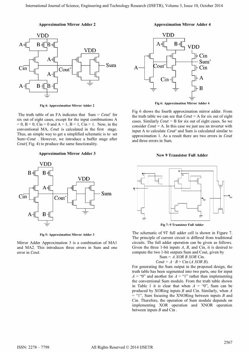
Approximation Mirror Adder 2
Fig 4: Approximation Mirror Adder 2
The truth table of an FA indicates that Sum = 𝐶𝑜𝑢𝑡' for
six out of eight cases, except for the input combinations A
= 0, B = 0, Cin = 0 and A = 1, B = 1, Cin = 1. Now, in the
conventional MA, 𝐶𝑜𝑢𝑡 is calculated in the first stage.
Thus, an simple way to get a simplified schematic is to set
Sum=𝐶𝑜𝑢𝑡 . However, we introduce a buffer stage after
𝐶𝑜𝑢𝑡( Fig. 4) to produce the same functionality.
Approximation Mirror Adder 3
Fig 5: Approximation Mirror Adder 3
Mirror Adder Approximation 3 is a combination of MA1
and MA2. This introduces three errors in Sum and one
error in 𝐶𝑜𝑢𝑡.
Approximation Mirror Adder 4
Fig 6: Approximation Mirror Adder 4
Fig 6 shows the fourth approximation mirror adder. From
the truth table we can see that 𝐶𝑜𝑢𝑡 = A for six out of eight
cases. Similarly 𝐶𝑜𝑢𝑡 = B for six out of eight cases. So we
consider 𝐶𝑜𝑢𝑡 = A. In this case we just use an inverter with
input A to calculate 𝐶𝑜𝑢𝑡' and Sum is calculated similar to
approximation 1. As a result there are two errors in 𝐶𝑜𝑢𝑡 and three errors in Sum.
New 9 Transistor Full Adder
Fig 7: 9 Transistor Full Adder
The schematic of 9T full adder cell is shown in Figure 7.
The principle of current circuit is differed from traditional
circuits. The full adder operation can be given as follows.
Given the three 1-bit inputs A, B, and Cin, it is desired to
compute the two 1-bit outputs Sum and Cout, given by Sum = A XOR B XOR Cin.
𝐶𝑜𝑢𝑡 = A · B + Cin (A XOR B).
For generating the Sum output in the proposed design, the
truth table has been segmented into two parts, one for input
A = ―0‖ and another for A = ―1‖ rather than implementing
the conventional Sum module. From the truth table shown
in Table 1 it is clear that when A = ―0‖, Sum can be
produced by XORing inputs B and Cin. Similarly, when A
= ―1‖, Sum focusing the XNORing between inputs B and
Cin. Therefore, the operation of Sum module depends on
implementing XOR operation and XNOR operation between inputs B and Cin .

International Journal of Science, Engineering and Technology Research (IJSETR), Volume 3, Issue 10, October 2014
2568
ISSN: 2278 – 7798 All Rights Reserved © 2014 IJSETR
III. Simulation Results
Tanner Tools was used for design, simulation and power
calculation. S-Edit was used for designing the mirror adder
circuits. W-Edit was used for waveform generation and T-
Spice was used for power computation. Finally these
results were compared to reach the conclusion.
Fig 8. Conventional MA Schematic
Fig 9. Conventional MA Waveform
Fig 10. Conventional MA Power
Fig 11: MA 4 Schematic
Fig 12: MA 4 Waveform
Fig 13: 9T Full adder
Fig 14: 9T Full Adder output waveform
Simulation Results (Power Comparison)
Design Average Power consumption
Conventional Mirror Adder 2.776267e-005 Watts
Approximation Adder-1 1.009787e-004 Watts
Approximation Adder-2 1.207350e-005 Watts
Approximation Adder-3 1.124363e-005 Watts
Approximation Adder-4 5.969556e-006 Watts
New 9T Full Adder design 3.301158e-008 Watts

International Journal of Science, Engineering and Technology Research (IJSETR), Volume 3, Issue 10, October 2014
2569
ISSN: 2278 – 7798 All Rights Reserved © 2014 IJSETR
IV. Conclusion
In this paper, we proposed several imprecise or
approximate adders that can be effectively utilized to trade
off power and quality for error-resilient DSP systems. Our
approach aimed to simplify the complexity of a
conventional MA cell by reducing the number of
transistors and also the load capacitances. When the errors
introduced by these approximations were reflected at a
high level in a typical DSP algorithm, the impact on output quality was very little. Note that our approach differed
from previous approaches. A decrease in the number of
series connected transistors helped in reducing the effective
switched capacitance and achieving voltage scaling. We
also derived simplified mathematical models for error and
power consumption of an approximate RCA using the
approximate FA cells. Using these models, we discussed
how to apply these approximations to achieve maximum
power savings subject to a given quality constraint.
FUTURE WORK
The future work aims at further reducing the transistor
count to six transistors to achieve even better power and
space efficiencies.
REFERENCES
[1] J. Han and M. Orshansky, ―Approximate computing: an emerging
paradigm for energy-efficient design,‖ in ETS’13, May 2013.
[2] R. Hegde and N.R. Shanbhag, ―Soft digital signal processing,‖ IEEE
Trans. VLSI Syst., vol. 9, no. 6, pp. 813–823, 2001.
[3] Vaibhav Gupta, Debabrata Mohapatra, Anand Raghunathan," Low-
Power Digital Signal Processing Using Approximate Adders" IEEE Trans.
on CAD Of IC and Systems, vol. 32, no. 1, Jan 2013.
[4] P. Kulkarni, P. Gupta, and M. Ercegovac, ―Trading accuracy for power
with an underdesigned multiplier architecture,‖ in Proc. 24th IEEE Int.
Conf. VLSI Design, Jan. 2011, pp. 346–351.
[5] V. Gupta, D. Mohapatra, S. P. Park, A. Raghunathan, and K. Roy,
―IMPACT: Imprecise adders for low-power approximate computing,‖ in
Proc. IEEE/ACM Int. Symp. Low-Power Electron. Design, Aug. 2011, pp.
409–414.
[6] D. Shin and S. K. Gupta, ―Approximate logic synthesis for error
tolerant applications,‖ in Proc. Design, Automat. Test Eur., 2010, pp.
957–960.
[7] H. R. Mahdiani, A. Ahmadi, S. M. Fakhraie, and C. Lucas, ―Bio-
inspired imprecise computational blocks for efficient VLSI
implementation of soft-computing applications,‖ IEEE Trans. Circuits
Syst. Part I, vol. 57, no. 4, pp. 850–862, Apr. 2010.
[8] Y. V. Ivanov and C. J. Bleakley, ―Real-time h.264 video encoding in
software with fast mode decision and dynamic complexity control,‖ ACM
Trans. Multimedia Comput. Commun. Applicat., vol. 6, pp. 5:1–5:21, Feb.
2010.
[9] M. Shafique, L. Bauer, and J. Henkel, ―enBudget: A run-time adaptive
predictive energy-budgeting scheme for energy-aware motion estimation
in H.264/MPEG-4 AVC video encoder,‖ in Proc. Design, Automat. Test
Eur., Mar. 2010, pp. 1725–1730.
[10] E. Lyons, V. Ganti, R. Goldman, V. Melikyan, and H. Mahmoodi,
―Full-custom design project for digital VLSI and IC design courses using
synopsys generic 90nm CMOS library,‖ in Proc. IEEE Int. Conf.
Microelectron. Syst. Edu., Jul. 2009, pp. 45–48.
[11] J. Choi, N. Banerjee, and K. Roy, ―Variation-aware low-power
synthesis methodology for fixed-point FIR filters,‖ IEEE Trans. Comput.-
Aided Des. Integr. Circuits Syst., vol. 28, no. 1, pp. 87– 97, Jan. 2009.
[12] G. Karakonstantis, D. Mohapatra, and K. Roy, ―System level DSP
synthesis using voltage overscaling, unequal error protection and adaptive
quality tuning,‖ in Proc. IEEE Workshop Signal Processing Systems,Oct.
2009, pp. 133–138.
[13] W. Dally, J. Balfour, D. Black-Shaffer, J. Chen, R. Harting, V.
Parikh,J. Park, and D. Sheffield, ―Efficient embedded computing,‖
Computer,vol. 41, no. 7, pp. 27–32, Jul. 2008