a novel application of zero-current-switching
TRANSCRIPT

Hindawi Publishing CorporationMathematical Problems in EngineeringVolume 2011, Article ID 481208, 16 pagesdoi:10.1155/2011/481208
Research ArticleA Novel Application ofZero-Current-Switching QuasiresonantBuck Converter for Battery Chargers
Kuo-Kuang Chen
Department of Electrical Engineering, Far East University, Tainan city 744, Taiwan
Correspondence should be addressed to Kuo-Kuang Chen, [email protected]
Received 24 April 2011; Accepted 27 May 2011
Academic Editor: Xing-Gang Yan
Copyright q 2011 Kuo-Kuang Chen. This is an open access article distributed under the CreativeCommons Attribution License, which permits unrestricted use, distribution, and reproduction inany medium, provided the original work is properly cited.
The main purpose of this paper is to develop a novel application of a resonant switch converter forbattery chargers. A zero-current-switching (ZCS) converter with a quasiresonant converter (QRC)was used as the main structure. The proposed ZCS dc–dc battery charger has a straightforwardstructure, low cost, easy control, and high efficiency. The operating principles and designprocedure of the proposed charger are thoroughly analyzed. The optimal values of the resonantcomponents are computed by applying the characteristic curve and electric functions derivedfrom the circuit configuration. Experiments were conducted using lead-acid batteries. The optimalparameters of the resonance components were determined using the load characteristic curvediagrams. These values enable the battery charger to turn on and off at zero current, resultingin a reduction of switching losses. The results of the experiments show that when comparedwith the traditional pulse-width-modulation (PWM) converter for a battery charger, the buckconverter with a zero- current-switching quasiresonant converter can lower the temperature ofthe activepower switch.
1. Introduction
Batteries are extensively utilized in many applications, including renewable energy genera-tion systems, electrical vehicles, uninterruptible power supplies, laptop computers, personaldigital assistants, cell phones, and digital cameras. Since these appliances continuouslyconsume electric energy, they need charging circuits for batteries. Efficient charging shortensthe charging time and extends the battery service life, while harmless charging prolongs thebattery cycle life and achieves a low battery operating cost. Moreover, the charging timeand lifetime of the battery depend strongly on the properties of the charger circuit. Thedevelopment of battery chargers is important for these devices. A good charging method canenhance battery efficiency, prolong battery life, and improve charge speed. Several chargingcircuits have been proposed to overcome the disadvantages of the traditional battery charger.

2 Mathematical Problems in Engineering
Have a crossing and produceswitching loss
turn on
OFF ON
t
VC(t), iC(t) VC(t) and iC(t)
VC(t)iC(t)
Figure 1: The switching loss of a traditional PWM power transistor.
The linear power supply is the simplest. A 60-Hz transformer is required to deliver the outputwithin the desired voltage range. However, the linear power supply is operated at the linefrequency, which makes it large both in size and weight. Besides, the system conversionefficiency is low because the transistor operates in the active region. Hence, when higherpower is required, the use of an overweighted and oversized line-frequency transformermakes this approach impractical. The high-frequency operation of the conventional convertertopologies depends on a considerable reduction in switching losses to minimize size andweight. Many soft-switching techniques have been proposed in recent years to solve theseproblems. Neti R. M. Rao developed the traditional pulse width modulation (PWM) powerconverter in 1970. PWM was used to control the turn-on-time of the power transistors toachieve the target of voltage step-up and step-down. The switching loss of traditional PWMconverters is shown in Figure 1, where VC(t) is the voltage across both the collector andemitter of the transistor, and iC(t) is the current across the collector of the transistor.
The advantages and drawbacks of this modulation style are addressed as follows.Advantages
(1) A high switching frequency can reduce the volume of magnetic elements andcapacitors.
(2) Power transistors are operated in the saturation region and cut-off region. Thismakes the power loss of the power transistors nearly zero.
Drawbacks
(1) The power is still restrained voltage and current during switching period, resultingin switching losses.
(2) Fast switching can result in serious spike current (di/dt), voltage (dv/dt), andelectromagnetic interference (EMI).
The control switches in all the PWM dc-dc converter topologies operate in a switchmode, in which they turn a whole load current on and off during each switching. Thisswitch-mode operation subjects the control switches to high switching stress and highswitching power losses. To maximize the performance of switch-mode power electronicconversion systems, the switching frequency of the power semiconductor devices needs tobe increased, but this results in increased switching losses and electromagnetic interference.To eradicate these problems, soft switching and various charger topologies more suitablefor battery energy storage systems have been presented and investigated. Zero-voltage-switching (ZVS) and zero-current-switching (ZCS) techniques are two conventionallyemployed soft-switching methods. These techniques lead to either zero voltage or zerocurrent during switching transition, significantly decreasing the switching losses and

Mathematical Problems in Engineering 3
Have a crossing and produceswitching loss
turn on
OFF ON
t
VC(t), iC(t)
VC(t) iC(t)
VC(t) and iC(t)
Figure 2: The switching loss of resonant power transistor.
increasing the reliability for the battery chargers. The ZVS technique eliminates capacitiveturn-on losses and decreases the turnoff switching losses by slowing down the voltage rise,thereby lowering the overlap between the switch voltage and the switch current. However,a large external resonant capacitor is needed to lower the turnoff switching loss effectivelyfor ZVS. Conversely, ZCS eliminates the voltage and current overlap by forcing the switchcurrent to zero before the switch voltage rises, making it more effective than ZVS in reducingswitching losses, particularly for slow switching power devices. For high-efficiency powerconversion, the ZCS topologies are most frequently adopted.
This paper adopts zero-current-switching (ZCS) converter with quasiresonant con-verter (QRC) as the main structure to charge a lead-acid battery. The resonant phenomena ofZCS converter with QRC is used to determine the switching loss of the switch. TraditionalPWM power converters have nonideal power loss during switching procedure. A capacitorin parallel with the switch is adopted in the proposed structure. Both the inductor andcapacitor resonate to make the current into sine waves. This can reduce the overlap areaof the voltage and current waves, decreasing switching loss. The switching loss of a resonantpower converter is shown in Figure 2.
In the attempt to overcome the tradition PWM converters, many efforts have beenmade to search a less expensive charger topology for batteries to offer a competitive price inthe consumer market. This paper presents a relatively simple topology for the battery chargerwith a ZCS quasiresonant buck converter, which is the most economical circuit topologycommonly used for driving low power energy storage systems. In the proposed approach,a resonant tank is interposed between the input dc source and the battery. With the addedresonant tank, the battery charger can achieve low switching loss with only one additionalactive power switch and easy control circuitry.
Power converters can be divided into the following types [1–8].
(1) Resonant Converter (RC): this converter uses both the half-bridge circuit and the full-bridge circuit as basic structures. It is implemented as a series resonant converter orparallel resonant converter.
(2) Quasiresonant Converter (QRC): this converter adopts both the half-wave stylecircuit and the full-wave style circuit as basic structures. It is implemented as aZCS converter or zero voltage switching (ZVS) converter.
(3) Multiresonant Converter (MRC): this converter adopts both a ZCS circuit and apartial resonant ZVS circuit in the half-bridge style DC-DC converter as basicstructures.
The advantages and drawbacks of resonant power converters are given below.Advantages: the power transistor has no voltage or current during the switching
process. It can reduce switching loss and restrain EMI effectively.
4 Mathematical Problems in Engineering
Vs
turn on
Is0
turn off
VC
iC
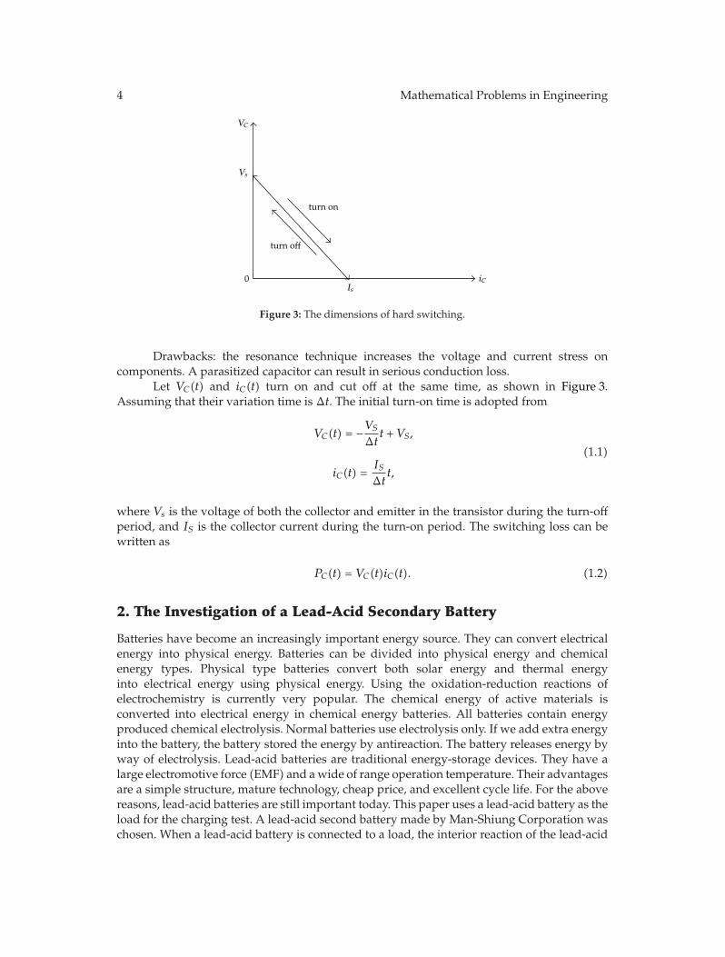
Figure 3: The dimensions of hard switching.
Drawbacks: the resonance technique increases the voltage and current stress oncomponents. A parasitized capacitor can result in serious conduction loss.
Let VC(t) and iC(t) turn on and cut off at the same time, as shown in Figure 3.Assuming that their variation time is Δt. The initial turn-on time is adopted from
VC(t) = −VS
Δtt + VS,
iC(t) =ISΔt
t,
(1.1)
where Vs is the voltage of both the collector and emitter in the transistor during the turn-offperiod, and IS is the collector current during the turn-on period. The switching loss can bewritten as
PC(t) = VC(t)iC(t). (1.2)
2. The Investigation of a Lead-Acid Secondary Battery
Batteries have become an increasingly important energy source. They can convert electricalenergy into physical energy. Batteries can be divided into physical energy and chemicalenergy types. Physical type batteries convert both solar energy and thermal energyinto electrical energy using physical energy. Using the oxidation-reduction reactions ofelectrochemistry is currently very popular. The chemical energy of active materials isconverted into electrical energy in chemical energy batteries. All batteries contain energyproduced chemical electrolysis. Normal batteries use electrolysis only. If we add extra energyinto the battery, the battery stored the energy by antireaction. The battery releases energy byway of electrolysis. Lead-acid batteries are traditional energy-storage devices. They have alarge electromotive force (EMF) and awide of range operation temperature. Their advantagesare a simple structure, mature technology, cheap price, and excellent cycle life. For the abovereasons, lead-acid batteries are still important today. This paper uses a lead-acid battery as theload for the charging test. A lead-acid second battery made by Man-Shiung Corporation waschosen. When a lead-acid battery is connected to a load, the interior reaction of the lead-acid

Mathematical Problems in Engineering 5
Negativeelectrode Electrolyte Positive
electrode
2H2O
4H2O
−−4H+
++
4OH −
Pb
Pb ++Pb
2e2e
PbO22H2SO4
Pb++++
PbSO4 PbSO4
SO4−−
SO4
Figure 4: Discharge reaction.
battery is the discharge reaction. The chemical reaction is described in [9]
PbO2 + Pb2+ + 2H2SO4 + 2e− =⇒ 2PbSO4 + 2H2O. (2.1)
As shown in Figure 4, lead-acid batteries produce both lead sulfate and water duringthe discharge period. At the positive electrode, lead dioxide reacts with sulfuric acid in theelectrolyte during the discharge period. Sulfuric acid is decomposed at the electrode. Sulfuricacid reacts with lead dioxide, which is the activated material at the positive electrode. Thisreaction produces lead sulfate, which sinks and piles up at the electrode. Lead, the activatedmaterial, reacts with sulfuric acid in the electrolyte at the negative electrode. Lead sulfateis produced from the above reaction. Then, lead sulfate sinks and piles up at the electrode.In the electrolyte, sulfuric acid is decomposed by reactions with the activated material atboth the positive and negative electrodes. The reaction reduces the electrolyte concentration.A lot of lead sulfate sinks and piles up at both the positive and negative electrodes. Thisreaction increases the interior resistance of the battery and decreases the voltage of the leadacid battery. As shown in Figure 5, the lead-acid battery recharges when it is discharged to acertain level. The interior reaction of the battery is the charging reaction, as shown in
2PbSO4 + 2H2O =⇒ PbO2 + 2H2SO4 + Pb. (2.2)
At both the positive and negative electrodes, the charge electrical energy of the exteriorsupply produces lead sulfate that is needed during the discharge period. After the abovereaction, the activated material, lead dioxide, is deposed at the positive electrode. Leadreacts with sulfuric acid in the electrolyte at the negative electrode at same time. Theirreactions increase the electrolyte concentration and raise voltage. In a lead-acid battery, theelectrochemistry reactions of both charging and discharging are reversible. This is the so-called “Double Sulfate Theory.” It can be expressed as
PbO2 + 2H2SO4 + Pb ⇐⇒ 2PbSO4 + 2H2O. (2.3)
The water production in lead-acid batteries during the discharge period is reelectrol-ysis by means of the charging reaction. From the above reactions, oxide is produced at the

6 Mathematical Problems in Engineering
Negativeelectrode Electrolyte Positive
electrode
2e
4H2O
4H2OPbO2
−−4
SO −−42H+ 2H+
Pb++++
PbSO4
++Pb4OH −
++
Pb
Pb
2e
H2SO4 H2SO4
PbSO4
SO
Figure 5: Charge reaction.
+
+
+
+
−
−
−
−
Cr iCr
iLr Lr Lf
Dmvx Cf
Lead-acidbattery
i0 ≈ I0
Q
Vin
VGS
VCr
VBA
Figure 6: The ZCS QRC charger.
positive electrode, and hydrogen is produced at the negative electrode at the same time.This prevents water loss from the electrolyte in a closed lead-acid battery. Oxide is producedfrom the positive electrode during the charging period; the activated material, that is, lead, isobtained from the negative electrode. The twomaterials above react to make leadmonooxide.Lead monooxide reacts with the sulfuric acid of lead sulfuric acid. Oxide produced from thepositive electrode during the charging period is absorbed by the negative electrode. The oxidedoes not leave from the battery, resulting in water loss in the electrolyte.
In order to charge a battery properly, four charge modes should be designed andimplemented in sequence, which are trickle charge, bulk charge, overcharge, and float charge.At the beginning of charge process, the trickle charge mode is adopted. And a very lowconstant current is applied to the battery to raise the voltage to the deep discharge threshold.Then the mode is switched into bulk charge. At the stage, a constant current is applied tothe battery with the purpose of quickly replenishing electricity to the battery. When thevoltage of battery exceeds overcharge limits, it enters into overcharge mode. In this modea constant voltage is applied to the battery, and its value is typically set between 2.45V/celland 2.65V/cell. Float charge is also a constant voltage charge mode after completing chargeprocess to maintain the capacity of the battery against self-discharge.
3. ZCS-QRC Buck Converter for a Battery Charger
A variety of driving circuits have been employed for the ZCS quasiresonant buck converter.Conventionally, the trigger signal is associated with a proper duty cycle to drive the

Mathematical Problems in Engineering 7
0
0
0
Ta Tb
Ts
Tc Td
t0 t1 t2 t3 t4
1 2 3 4
t
t
tiLr
I0 Z0
−
t1′′t1′
Vin
Vin
Vin
VGS
Crv
Figure 7: Timing and waveform diagram.
active power switch with the required charging current. The major elements of the ZCSquasiresonant buck converter for battery charger are available in a single integrated circuit.The integrated circuit contains an error amplifier, sawtooth waveform generator, andcomparator for PWM. The turn-on and turn-off of the ZCS-QRC switch is operated whenthe current is zero. The produced current that is resonated by Lr and Cr passes through theswitch. Because Lr is very large, io is assumed to be a constant Io. The circuit structure isshown in Figure 6. In addition, the steady-state waveform is shown in Figure 7.
The following assumptions are made
(1) All semiconductor elements are ideal. This means that switches have no time delayduring the switching period.
(2) There is no forward voltage drop in the diodeDm during the turn-on period. Thereis no leakage current during the turn-off period.
(3) The inductor and capacitor of the tank circuit have no equivalent series resistance(ESR).
(4) The filtering inductor Lf � Lr the filtering capacitor Cf � Cr . Because the cut-offfrequency of current that is composed of low pass filter circuit load and filteringcapacitor Cr is much less than the resonant phase angle frequency ωo = 1/
√LrCr
of resonant circuit that is composed by resonant inductor Lr and resonant capacitorCr . Compared to the resonant circuit, the filtering circuit composed of Lf and Cf
and the load can be regarded as a constant current source Io.
(5) Unregulated line voltage Vin does not significantly vary during the resonant circuitturn-on and turn-off period Ts.Vin is regarded as a constant.
The operation of the complete circuit is divided into four modes.

8 Mathematical Problems in Engineering
Cr
Cr
iLrLr
I0Dm
+ −
+−
v
Vin
Figure 8: The equivalent circuit of Mode 1.
Mode 1 [linear stage (t0 ≤ t ≤ t1)]
Before turning on the switch, the output current Io passes through diode Dm. Thus, thevoltage across Cr makes vCr = Vin. Thus, the initial conditions are iLr = 0 and vCr = Vin.The current that passes through the switch is zero at t = t0. The switch Q is turned on at thesame time t = t0 with ZCS. Diode Dm is also turned on simultaneously. The inductor currentiLr(t) is increased linearly. If iLr is less than Io, The freewheel diode Dm is still turned on, andvCr is maintained at Vin, as shown in Figure 8. The circuit equation is represented as
iLr(t) =Vin
Lrt. (3.1)
This mode is finished when iLr(t) is equal to Io at t = t1. The period of Mode 1 can becalculated by
Ta =IoLr
Vin. (3.2)
At t = t1, diode Dm is turned off. Then, the mode enters to Mode 2.
Mode 2 [resonant stage t1 ≤ t ≤ t2]
Lr and Cr resonate at this stage. The peak value of iLr is Vin/Zo + Io, and vCr is equal to zeroat t = t1. The negative peak value of vCr occurs when iLr is equal to Io at t = t1. iLr is decreasedto zero at t = t2. The switch Q is turned off automatically due to the forward direction, asshown in Figure 9. The equations of the circuit are shown as
vCr(t1) = Vin, (3.3)
iLr(t) = Io +Vin
Zosinωo(t − t1) (3.4)
Substituting formula (3.4) into formula (3.3) and yielding
vCr(t) = Vin cosωo(t − t1). (3.5)

Mathematical Problems in Engineering 9
vCr
Cr
iLrLr
I0
+ −
+−
Vin
Figure 9: The equivalent circuit of Mode 2.
As a result, both Lr and Cr form a resonant path. From (3.4), it is necessary to haveZoIo < Vin to confirm with ZCS at this moment. Mode 2 is finished at t = t2, when the peakvalue of the capacitor voltage vCr(pk) is equal to –Vin. The period of Mode 2 is calculated by
Tb =
[sin−1((ZoIo)/Vin) + π
]
ωo. (3.6)
The pulse trigger of switch Q is eliminated, and Mode 3 is entered at t = t2.
Mode 3 [recovery stage (t2 ≤ t ≤ t3)]
The equivalent circuit of Mode 3 is shown in Figure 10. Io passes through Cr . So vCr isincreased linearly at this stage. The circuit equation is presented as
vCr(t) =IoCr
(t − t2) + Vin cosωo(t2 − t1). (3.7)
vCr(t3) can be calculated by substituting t = t3 into formula (3.7); therefore
vCr(t3) =IoCr
(t3 − t2) + Vin cosωo(t2 − t1). (3.8)
Due to vCr(t3) = Vin, the following equation can be obtained from formula (3.8):
t3 − t2 =(VinCr
Io
)[1 − cosωo(t2 − t1)]. (3.9)
Thus, the period of Mode 3 can be represented as
Tc =(VinCr
Io
)[1 − cosωo(t2 − t1)]. (3.10)
Mode 3 is finished at t = t3. So Dm is turned on at this moment, and enter to Mode 4.

10 Mathematical Problems in Engineering
+−
vCr
Cr
Lr
I0
+ −
iCr
Vin
Figure 10: The equivalent circuit of Mode 3.
vCr
Cr
Lr
I0Dm
+ −
+−Vin
Figure 11: The equivalent circuit of Mode 4.
Mode 4 [freewheeling stage (t3 ≤ t ≤ t4)]
At this stage, the switchQ is still controlled under the turn-off condition. DiodeDm is turnedon and is formed of the Io loop, as shown in Figure 11. At t = t4, the switch Q is triggeredagain. Then, the next cycle begins. If we can control the period of the freewheeling stage, wecan regulate the output voltage. The circuit equation is described by
Td = Ts − (Ta + Tb + Tc). (3.11)
The capacitor and inductor do not consume power in the ideal condition. In the idealcondition, no energy is wasted in switch element, transistor, or diode. Neither the capacitornor inductor has a parasitic resistor in the ideal condition. The supply energy of the powersource is equal to the absorbing energy of the load in a cycle. The circuit equation is shown as
Vin
∫ t1
0
Vin
Lrtdt +
∫ t2
t1
[Io +
Vin
Zosinωo(t − t1)
]dt =
VoIofs
,
Vo = Vinfs
{Vin
IoLr
(t212
)
+ (t2 − t1) +Vin
IoZoωo[1 − cosωo(t2 − t1)]
}
.
(3.12)

Mathematical Problems in Engineering 11
After rearrangement, the average value of output voltage Vo can be derived by
Vo = Vinfs
[(t12
)+ (t2 − t1) + (t3 − t2)
]. (3.13)
According to above condition, formula (3.13) can be rewritten as
Vo = Vinfs
[(Ta2
)+ Tb + Tc
]. (3.14)
The voltage average value of the filtering inductor is equal to zero in steady state. Theaverage voltage of vCr is exactly equal to the output voltage Vo. We can modulate the valueof the output voltage Vo by controlling the period of Mode 4 (i.e., changing the switchingfrequency). From the waveforms of Figure 7, we can get the characteristics of the device.
(1) Both turn-on and turn-off of the switch are ZCS in order to reduce the switchingloss of the switch element.
(2) The load current Io must be less than Vin/Zo to confirm ZCS of the switch duringthe turn-off period.
(3) Increasing Io will result in a reduced Vo during the constant frequency operationperiod. We can regulate Vo by increasing ωo. We can reduce ωo to modulate Vo
during the Io decreasing period.
(4) If the switch is parallel to an antiparallel diode, the inductor current can reverse thecurrent direction. The energy stored in the resonant circuit will be sent back to Vo.
The converter can be operated in a very high frequency region due to reducedswitching loss and EMI.
4. The Element Design of the Charger in a ZCSQuasiresonant Buck Converter
Compared to a traditional PWM converter, the switching loss of a ZCS quasiresonant buckconverter is low. This paper adopts the charger of a ZCS quasiresonant buck converter. Asshown in Figure 6, a resonant capacitor Cr and a resonant inductor Lr were added to reducethe switching loss of switch Q in the traditional PWM Buck converter circuit. According tothe results of the operation stage analysis, we can design the resonant elements (i.e., resonantcapacitor Cr and resonant inductor Lr). According to the charger’s energy balance of the ZCSquasiresonant buck converter in Figure 6, neither capacitor nor inductor consumes averageenergy in the ideal condition. There is no energy consumption in the switch element, transis-tor, or diode during the ideal condition. Thus, the supply energy of the power source is equalto the absorbing energy of the load. The supply energy of power source can be written as
Ein =∫TS
0= Pin(t)dt = Vin
∫TS
0iLr(t)dt. (4.1)

12 Mathematical Problems in Engineering
1
0.9
0.8
0.7
0.6
0.5
0.4
0.3
0.2
0.1
010.90.80.70.60.50.40.30.20.10
I0Z0/V
fs/fr = 0.75
fs/fr = 0.5
fs/fr = 0.35
fs/fr = 0.25
fs/fr = 0.15
fs/fr = 0.05
V0/
Vi n
in
Figure 12: The load characteristics curve.
The absorbing energy of the load can be calculated by
Eo =∫TS
0Po(t)dt = VoIoTs. (4.2)
If we neglect the power consumption of the converter, we can assign the normalizationof load resistor r = Ro/Zo and the ratio of the output voltage X = Vo/Vin. We can obtainformula (4.3) after simplification at α = ωo(t2 − t1):
Vo
Vin=
fs2πfr
⎧⎨
⎩X
2r+ π + sin−1
[X
r
]+
r
X
⎡
⎣1 +
√
1 −(X
r
)2⎤
⎦
⎫⎬
⎭. (4.3)
After converting formula (4.3) appropriately, we can get the curve sketch of the loadcharacteristics as Figure 12 [10].
MATLAB simulation software was used to sketch the curve plot. Because the ZCSquasiresonant converter must be suitable for ZoIo < Vin, this paper adopts the curve forwhich the ratio of the output and input is the closest to 1. fs/fr is chosen to be 0.75. Theswitching frequency is equal to 22.72 kHz. The resonant frequency is 30 kHz. With ZoIo < Vin,Io is designed to equal 0.4A, and Vin is equal to 24V. After calculating, we get Cr > 88.49 nFand Lr < 318 uH. One adopts Cr = 0.1 uF and Lr = 300 uH.
5. Experiment Results and Discussion
This study includes circuit simulations using Pspice software and practically implementsthe developed novel charger. Finally, the simulated and practical results are compared.The battery charger characteristics of a resonant switching converter were investigated.

Mathematical Problems in Engineering 13
15
10
5
020 40 60 80 1000
VGS
V
(μs)
()
(a)
20 40 60 800
vCr
−40
−60
V 0
40
60
100(μs)
()
(b)
20 40 60 80 1000
0.4
0.2
0
A
−0.2
iLr
(μs)
()
(c)
VGS
vCr
iLr
Q Controlsignal
20V/div
50V/div
1A/div
Time (10μs/div)
(d)
Figure 13: Waveforms of VGS, vCr , and iLr (a) simulated waveform of VGS (b) simulated waveform of vCr
(c) simulated waveform of iLr (d) practical waveform of VGS, vCr , and iLr .
20 40 60 80 1000
vx0
−20
20
40
60
V
(μs)
()
(a)
20V/divvx
Time (10μs/div)
(b)
Figure 14: The voltage waveforms of diode Dm (a) simulated waveform (b) measured waveform.
The resonant waveforms of the chargers, the curve charts of the charging periods, and thetemperature curves were compared. For the experiment, the DC input voltage was 24V, theswitching frequency of the switch was 22.72 kHz, the resonant frequency was 30 kHz, thecharging current was 0.4A, the charging voltage was 16V, and the open circuit voltage was11.7V. Figure 13 shows the simulated and practical waveforms of the main switch triggered

14 Mathematical Problems in Engineering
20 40 60 8000
100(μs)
V()
15
10
5
VBA
(a)
20 40 60 80 1000
(μs)
0
1
0.5A() I0
(b)
5V/div
0.5V/div
I0
VBA
Time (10μs/div)
(c)
Figure 15: The waveforms of battery charging voltage and charging current (a) simulated waveform ofoutput voltage (b) simulated waveform of output current (c) measured waveforms of charging voltageand charging current.
0
16
14
12
1060 120 180 240 300
Battery
voltag
eV()
Charge time (min)
Figure 16: The elevated curves of battery voltage.
signal VGS, the resonant capacitor voltage vCr , and the resonant inductor current iLr duringthe charging period. Compared to Figure 6, the turn-on and turn-off operation of the mainswitch is at the zero-current condition. The switching loss of the switch is lower than those ofhard-switching ones.
Figures 14(a) and 14(b) plot the voltage waveforms of diodeDm. The battery chargingvoltage and charging current are shown in Figure 15. With a 0.5A constant current, it takes180 minutes for the voltage of the lead-acid battery to reach 14V, as shown in Figure 16.

Mathematical Problems in Engineering 15
Tempe
rture
The temperature curve plot of traditionalPWM switching converter charger
The temperture curve plot of ZCS charger
60
50
40
30
20
100 15 30 45 60 90 120 150 180 210 240
(◦C)
Charge time (min)
Figure 17: A comparison of power switch temperature curves.
A temperature curve comparison chart between the ZCS converter charger andtraditional PWM switching ones is shown in Figure 17. A temperature comparison of thepower switch is also shown in Figure 17 at the same test conditions (same output andinput voltages, lead-acid battery, filtering inductor, and filtering capacitor). The chargertemperature of the ZCS converter was kept at 32◦C after a certain period. This can verifythat ZVS can reduce the power loss of the power switch.
6. Conclusion
This paper has developed a novel application of zero-current-switching buck dc–dc converterfor a battery charger. The circuit structure is simpler and much cheaper than other controlmechanisms requiring large numbers of components. From the results of the experiments,charger switch is turned on and off at the zero-current stage. Resonant switching improvesthe traditional hard-switching power loss produced by turning the switch on and off ata nonzero current stage and lowers the switch temperature to reduce power loss of thepower switch. From the measurements, the power switch transistor temperature of the ZCSconverter charger was kept at 31◦C after a certain period. Compared to a traditional hard-switching charger, the temperature of the power switch transistor of the proposed chargerwas much lower.
References
[1] Y. C. Chuang and Y. L. Ke, “A novel high-efficiency battery charger with a buck zero-voltage-switching resonant converter,” IEEE Transactions on Energy Conversion, vol. 22, no. 4, pp. 848–854,2007.
[2] C. Cutrona and C. di Miceli, “A unified approach to series,parallel and series-parallel resonantconverters,” in Proceedings of the 14th International Telecommunications Energy Conference (INTELEC ’92),pp. 139–146, 1992.
[3] M. Castilla, L. G. de Vicuna, J. M. Guerrero, J. Matas, and J. Miret, “Sliding-mode control of quantumseries-parallel resonant converters via input-output linearization,” IEEE Transactions on IndustrialElectronics, vol. 52, no. 2, pp. 566–575, 2005.
[4] M. K. Kazimierczuk, “Class D current-driven rectifiers for resonant DC/DC converter applications,”IEEE Transactions on Industrial Electronics, vol. 38, no. 5, pp. 344–354, 1991.
[5] K.H. Liu and F. C. Y. Lee, “Zero-voltage switching technique in DC/DC converters,” IEEE Transactionson Power Electronics, vol. 5, no. 3, pp. 293–304, 1990.
[6] M. K. Kazimierczuk, D. Czarkowski, and N. Thirunarayan, “New phase-controlled parallel resonantconverter,” IEEE Transactions on Industrial Electronics, vol. 40, no. 6, pp. 542–552, 1993.
[7] O. Dranga, B. Buti, and I. Nagy, “Stability analysis of a feedback-controlled resonant DC-DCconverter,” IEEE Transactions on Industrial Electronics, vol. 50, no. 1, pp. 141–152, 2003.

16 Mathematical Problems in Engineering
[8] J. G. Cho, J. W. Baek, G. H. Rim, and I. Kang, “Novel zero voltage transition PWM multi-phaseconverters,” in Proceedings of the IEEE 11th Annual Applied Power Electronics Conference and Exposition,(APEC ’96), pp. 500–506, March 1996.
[9] N. H. Kutkut, H. L. N. Wiegman, D. M. Divan, and D. W. Novotny, “Design considerations for chargeequalization of an electric vehicle battery system,” IEEE Transactions on Industry Applications, vol. 35,no. 1, pp. 28–35, 1999.
[10] T. T. Chieng, The Beginning of Novel Soft-Switching Power Supply, Chuan Hwa Book CO., LTD, Taiwan,2000.

Submit your manuscripts athttp://www.hindawi.com
Hindawi Publishing Corporationhttp://www.hindawi.com Volume 2014
MathematicsJournal of
Hindawi Publishing Corporationhttp://www.hindawi.com Volume 2014
Mathematical Problems in Engineering
Hindawi Publishing Corporationhttp://www.hindawi.com
Differential EquationsInternational Journal of
Volume 2014
Applied MathematicsJournal of
Hindawi Publishing Corporationhttp://www.hindawi.com Volume 2014
Probability and StatisticsHindawi Publishing Corporationhttp://www.hindawi.com Volume 2014
Journal of
Hindawi Publishing Corporationhttp://www.hindawi.com Volume 2014
Mathematical PhysicsAdvances in
Complex AnalysisJournal of
Hindawi Publishing Corporationhttp://www.hindawi.com Volume 2014
OptimizationJournal of
Hindawi Publishing Corporationhttp://www.hindawi.com Volume 2014
CombinatoricsHindawi Publishing Corporationhttp://www.hindawi.com Volume 2014
International Journal of
Hindawi Publishing Corporationhttp://www.hindawi.com Volume 2014
Operations ResearchAdvances in
Journal of
Hindawi Publishing Corporationhttp://www.hindawi.com Volume 2014
Function Spaces
Abstract and Applied AnalysisHindawi Publishing Corporationhttp://www.hindawi.com Volume 2014
International Journal of Mathematics and Mathematical Sciences
Hindawi Publishing Corporationhttp://www.hindawi.com Volume 2014
The Scientific World JournalHindawi Publishing Corporation http://www.hindawi.com Volume 2014
Hindawi Publishing Corporationhttp://www.hindawi.com Volume 2014
Algebra
Discrete Dynamics in Nature and Society
Hindawi Publishing Corporationhttp://www.hindawi.com Volume 2014
Hindawi Publishing Corporationhttp://www.hindawi.com Volume 2014
Decision SciencesAdvances in
Discrete MathematicsJournal of
Hindawi Publishing Corporationhttp://www.hindawi.com
Volume 2014
Hindawi Publishing Corporationhttp://www.hindawi.com Volume 2014
Stochastic AnalysisInternational Journal of