a new device with pzt ultrasonic transducers in mems - iopscience
TRANSCRIPT

Journal of Physics Conference Series
OPEN ACCESS
A new device with PZT ultrasonic transducers inMEMS technologyTo cite this article Soeren Hirsch et al 2006 J Phys Conf Ser 34 475
View the article online for updates and enhancements
You may also likePiezoelectric micro energy harvestersbased on stainless-steel substratesShun-Chiu Lin and Wen-Jong Wu
-
Fabrication of PZT MEMS energyharvester based on silicon and stainless-steel substrates utilizing an aerosoldeposition methodShun-Chiu Lin and Wen-Jong Wu
-
Fabrication and characterization of MEMS-based PZTPZT bimorph thick filmvibration energy harvestersR Xu A Lei C Dahl-Petersen et al
-
This content was downloaded from IP address 141331610 on 12022022 at 0959
A new device with PZT ultrasonic transducers in
MEMS technology
Soeren Hirsch1 Steffen Doerner Stefan Schimpf Ralf LucklumPeter Hauptmann and Bertram SchmidtOtto-von-Guericke University of Magdeburg Institute of Micro and Sensor Systems (IMOS)Uniplatz 2 39106 Magdeburg Germany
E-mail soerenhirschetuni-magdeburgde
Abstract Thick-film piezoelectric transducers have been produced and tested for implemen-tation into a MEMS ultrasonic sensor array The arrays are intended to be used for beamforming in sensing applications for fluidics in channels at millimeter or micrometer scale (egflow rate measurement detection of beads bubbles) Stripe and matrix aligned elements havebeen fabricated for one-dimensional and two-dimensional beam steering respectively In thiscontribution we further concentrate on an improved Q-factor and PZT layer homogeneity as amajor requirement for the transducer elements
1 IntroductionCurrently ultrasonic technology for microfluidics that is based on the thickness mode is mainlyused for fluid manipulating applications eg particle sorting mixing cell disruption anddeagglomeration [1][2][3] To establishing ultrasonic in-situ analyzing methods for microfluidics(concentration and flow rate measurement particle size distribution sound attenuationmeasurement) new sensor devices have to become available Many efforts have already beenspent on micromachined ultrasonic transducers for in-air use such as ultrasonic imaging or objectdetection [4][5] Ultrasonic transducer arrays employing capacitive actuators are available andhave been intensively studied in the past [6] For liquid analytes piezoelectric actuation providesbetter performance due to higher energy density It is impossible to use traditional PZT ceramicsto fabricate high frequency ultrasonic transducers because such high frequencies require thethickness of the PZT ceramic plates to be as thin as 50 m which is difficult to machine dueto its brittleness and poor mechanical strength [7] Piezocomposite technology that has beenmainly used for medical imaging can be impedance-matched to the analyte and driven with highexcitation voltages However combination of piezocomposite and MEMS technology requires aseparate mechanical processing To our knowledge integration onto a MEMS substrate has notyet been developed Combination of PZT thick-film [8] and silicon technology provides bothpiezoelectric actuation with a piezoceramic layer and micro machining of coupling membranes
1 Corresponding author Tel +49 39167 12392 Fax +49 39167 12609
Institute of Physics Publishing Journal of Physics Conference Series 34 (2006) 475ndash480doi1010881742-6596341078 International MEMS Conference 2006
475copy 2006 IOP Publishing Ltd
2 Design and fabrication21 Sensor designWith this sensor design the PZT transducers are operating as resonators in thickness mode - notas actuators to excite the eigenfrequencies of the silicon membrane Therefore it was mandatoryto design the sensor and membrane geometry without having an overlap between PZT transducerand system resonance Membrane shape and thickness have been optimized using ANSYS toanalyze the system frequencies and to reduce the cross coupling between single elements whilemaintaining required stiffness for the fluid channel First test samples were made with TiPtbottom electrodes on the silicon test wafers and structured with a lift-off process A multi-stagescreen printing process allowed creating layers of PZT with variable thickness between 30 mand 100 m The top electrodes have been formed by additional sputtering Fluid chamber andchannel were developed with the help of anodic bonding For special applications a packageis produced with MID (molded interconnect device) technology The MID technology permitsthe production of not-planar chip assembly substrates In order to contact the ultrasonic arrayelectrically and mechanically flip-chip technology was used This allows an integration of driverand amplifier electronics very close to the PZT elements and does not require an electricalimpedance matching for a coaxial cable connection
22 Device fabricationThe detailed fabrication process of the ultrasonic array is shown in Figure 1 Before starting thefabrication process the 4 inch silicon wafer was cleaned in acetone isopropanol and Carotlsquos acid(H2O2 H2SO4) and kept on a hotplate at 150 C for 20 min The first fabrication steps are(a) thermal wet and dry oxidation on both sides until the thickness of silicon oxide layer reaches500 nm and (b) backside etching of silicon oxide to open the etching window for the silicon
(c) Sputtering bottom electrodes
(d) Lift-off process
(b) Opening backside
(e) Multi-step screen print and annealing
(f) Sputtering top electrodes
(g) KOH wet etching
SiO2 + SiN4
Ti Pt
Cr Au
PZT
SiO2
Substrate
Photo resist
(a) Cleaning and thermal oxidation
Figure 1 Schematic diagram of the device fabrication process
476
(a) (b)
(c)
top electrode
Si
bottomelectrode
PZT
(d)
Figure 2 SEM scans of screen-printed PZT elements from different processing
diagram Then the lift-off resist TI35ES (Micro Chemicals) was deposited with spin coatingstructured with UV light and developed The bottom electrodes were deposited with sputtertechnology (c) For the connective layer titanium (100 nm) was sputtered at typical power levelThe platinum layer (400 nm) was sputtered at a higher power level The higher power led to abetter adhesion of the platinum to the titanium layer Then the sputtered layers were patternedwith lift-off method (d) to form the bottom electrodes
The PZT layers (e) were fabricated by screen printing The printing paste was made bymixing 80 of PZT powder (APC Piezokeramica 856) with 20 of lead oxide (PbO) and addinga solution of 4 ethyl-cellulose as an organic binder and 96 terpineol as a solvent the organicvehicle determines the flow properties of the paste and the bonding agent provides adhesion ofthe particles between each other and to the substrate [9][10][11] A 325 meshinch steel screenwas used Multiple printdryfire cycles were performed on the piezo-layers to achieve differentdry thicknesses Peak firing temperatures of 950 C were adopted for the conductors and thePZT paste respectively During the firing process the organic binder is burned metallic particlesare reduced or oxidized and glass particles are sintered Figure 2 shows SEM scans of producedelements with different paste preparation and processing parameters In (a) the whole elementis spoiled by blow holes This results from wrong binder type and mixing ratio After changingthe binder configuration (b) shows less blow holes but still appears open porous With modifiedprocessing parameters (eg firing temperature) a solid PZT element could be obtained (c) Thefinal configuration is shown in (d) that offers good homogeneity
Chromium (30 nm) and gold (100 nm) thin films are deposited on the front side by sputteringand are patterned by lift-off method to form the top electrodes (f) For the first experiments a
477
Figure 3 Fabricated ultrasonic test arrays in(a) stripe and (b) matrix configuration
Figure 4 Backside containing mem-branes of different thickness
highly conductive bonding epoxy H20-E (Epoxy Technology) has been used to contact the topelectrodes to the contact pads Finally (g) bulk silicon anisotropic wet etching with potassiumhydroxide (KOH) is used to produce the thin membrane structure The etching process wasperformed at a concentration of 30-wt and a temperature of 80 C After these fabricationprocesses piezoelectric activity was induced in the layers by applying a poling field of about4 MVm for 30 min at 150 C and maintaining it during cooling back to room temperature [12]
3 ExperimentalIn Figure 3 different fabricated ultrasonic transducer forms (squares stripes) for evaluating layeralignment as well annealing and polarization behavior are presented With the help of a whitelight profilometer (Fries Research amp Technology) the height profile as well as the roughness ofindividual elements was examined It could be stated that the height distribution remainedin its tolerances over the entire wafer However the roughness increased with the elementsbecoming smaller There were larger problems with decreasing of the pitch With screen printsa pitch of 500 m was reproducibly possible In order to employ smaller pitches a laser machinedstencil proceeded very well Additionally experiments have been performed to test the usabilityof photo resist as stencil that is spin coated on the wafer filled with PZT paste and removedduring the baking process For researching the influence of the membrane stiffness a testbench of membranes was developed Figure 4 shows single membranes membrane arrays andmembranes with MESA structures
31 Impedance spectrum analysisAn Agilent 4295A networkimpedance spectrum analyzer was used to acquire the admittancespectra of resonator test elements The system has been calibrated with a three-term calibrationat the test tips The measurements were performed to analyze the resonant frequency at differentPZT layer thickness as well the matching between elements on the same wafer Furthermore thequality factor of the fabricated PZT elements has been characterized Figure 5 shows exemplarilythe admittance plot for a single element (solid line) It has been processed with a six-strokescreen print This results in a final layer thickness of 110 m offering a series resonant frequencyof fs = 49 MHz The fabricated resonator offers a remarkably increased quality factor comparedto a commercially available PZ35 piezoceramic (Ferroperm) Measurements between resonatorson same wafers resulted in a tolerance for the series resonant frequency of less than 5 Thisclose tolerance is required for beam steering applications
478
(a) (b)
Figure 5 (a) conductance spectrum and (b) susceptance spectrum of the fabricated transducer(solid line fs = 49 MHz) in comparison to a commercially available PZ35 piezoceramic (dottedline fs = 245 MHz)
(a) (b)
(c) (d)
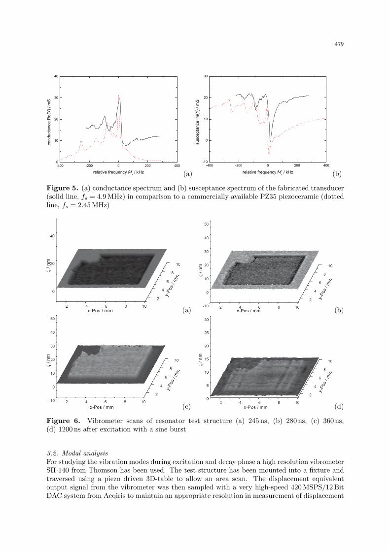
Figure 6 Vibrometer scans of resonator test structure (a) 245 ns (b) 280 ns (c) 360 ns(d) 1200 ns after excitation with a sine burst
32 Modal analysisFor studying the vibration modes during excitation and decay phase a high resolution vibrometerSH-140 from Thomson has been used The test structure has been mounted into a fixture andtraversed using a piezo driven 3D-table to allow an area scan The displacement equivalentoutput signal from the vibrometer was then sampled with a very high-speed 420 MSPS12 BitDAC system from Acqiris to maintain an appropriate resolution in measurement of displacement
479
and time Excitation voltage of the single sine burst was 40 V peak-to-peak with a frequencyof 5 MHz Figure 6 shows the vibrometer measurement results The first area scan (a) duringthe negative part of the excitation burst shows a consistent displacement ς across the elementrsquossurface This confirms the good homogeneity of the deposited PZT layer At the zero crossing (b)the displacement is still well consistent At the positive half wave (c) the edges already reveal thegeneration of the first radial wave After four periods within the decay phase (d) the dominatingradial wave with a wavelength of λ = 09 mm can be observed very well However the area scansdo not reveal a dominating bending wave that would degrade the emission behavior for the usein beam forming and beam steering applications The area of zero displacement in the upper leftcorner was caused by partial depolarization due to the applied soldering technique for contactingthe top electrode For subsequent test structures a low temperature bonding process is used
4 ConclusionPZT thick-film ultrasonic test arrays have been fabricated using a combined MEMS and multi-stage screen printing process Impedance and vibrometer measurements show the resonatorelements offering a high quality factor and a good homogeneity in the deposited PZT layersVarious shape types and pitch dimensions have been patterned with the multi-stage screenprinting process to test alignment and layer homogeneity capabilities of this method To avoida degrading influence of radial waves on beam steering accuracy and focusing resolution furthereffort will be put into damping of unwanted vibration modes Subsequent objectives will includea vibrometer setup for characterizing shear modes occurring in the resonator elements and aninter-element cross-coupling analysis between adjacent resonators
5 References
[1] Harris N Hill M Shen Y Townsend R J Beeby S and White N 2004 A dual frequency ultrasonicmicroengineered particle manipulator Ultrasonics 42 139ndash144
[2] Belgrader P Hansford D Kovacs G T A Venkateswaran K Mariella R Milanovich F Nasarabadi S OkuzumiM Pourahmadi F and Northrup M A 1999 A minisonicator to rapidly disrupt bacterial spores for DNAanalysis Analytical Chemistry 71 4232ndash36
[3] Nguyen N T and Wu Z 2005 Micromixersmdasha review J Micromech Microeng 15 R1ndashR16[4] Yamashita K Katata H Okuyama M Miyoshi H Kato G Aoyagi S and Suzuki Y 2002 Arrayed ultrasonic
microsensors with high directivity for in-air use using PZT thin film on silicon diaphragms Sensors andActuators A 97ndash98 302ndash307
[5] Baborowski J Muralt P Ledermann N Petitgrand S Bosseboeuf A Setter N and Gaucher P 2002 PZTcoated membrane structures for micromachined ultrasonic transducers Appl of Ferroelectrics ISAF 2002Proc of the 13th IEEE International Symposium on 483ndash486
[6] Jin X Oralkan O Degertekin F L and Khuri-Yakub B T 2001 Characterization of one-dimensional capacitivemicromachined ultrasonic immersion transducer arrays IEEE Trans Ultrason Ferroelect Freq Contr48 750ndash760
[7] Lukacs M Sayer M and Foster S 2000 Single element high frequency (lt50 MHz) PZT sol gel compositeultrasound transducers Ultrasonics Ferroelectrics and Frequency Control IEEE Transactions on 47 148ndash159
[8] Torah R Beeby S P and White N M 2005 An improved thick-film piezoelectric material by powder blendingand enhancement processing parameters IEEE Trans Ultrason Ferroelect Freq Contr 52 10ndash16
[9] De Cicco G Morten B and Prudenziati M 1994 Piezoelectric thick-film sensors Thick Film Sensors ed MPrudenziati (Amsterdam Elsevier) pp 209ndash28
[10] White N M and Ko V T K 1993 Thick-film acoustic wave sensor structure Electron Lett 29 (20) 1807ndash08[11] Moilanen H Leppavuori S and Usimaki A 1993 Sens Actuators A 37ndash38 106ndash11[12] Ferrari V Marioli D and Taroni A 1997 Thick-film resonant piezo-layers as new gravimetric sensors Meas
Sci Technol 8 42ndash48
480

A new device with PZT ultrasonic transducers in
MEMS technology
Soeren Hirsch1 Steffen Doerner Stefan Schimpf Ralf LucklumPeter Hauptmann and Bertram SchmidtOtto-von-Guericke University of Magdeburg Institute of Micro and Sensor Systems (IMOS)Uniplatz 2 39106 Magdeburg Germany
E-mail soerenhirschetuni-magdeburgde
Abstract Thick-film piezoelectric transducers have been produced and tested for implemen-tation into a MEMS ultrasonic sensor array The arrays are intended to be used for beamforming in sensing applications for fluidics in channels at millimeter or micrometer scale (egflow rate measurement detection of beads bubbles) Stripe and matrix aligned elements havebeen fabricated for one-dimensional and two-dimensional beam steering respectively In thiscontribution we further concentrate on an improved Q-factor and PZT layer homogeneity as amajor requirement for the transducer elements
1 IntroductionCurrently ultrasonic technology for microfluidics that is based on the thickness mode is mainlyused for fluid manipulating applications eg particle sorting mixing cell disruption anddeagglomeration [1][2][3] To establishing ultrasonic in-situ analyzing methods for microfluidics(concentration and flow rate measurement particle size distribution sound attenuationmeasurement) new sensor devices have to become available Many efforts have already beenspent on micromachined ultrasonic transducers for in-air use such as ultrasonic imaging or objectdetection [4][5] Ultrasonic transducer arrays employing capacitive actuators are available andhave been intensively studied in the past [6] For liquid analytes piezoelectric actuation providesbetter performance due to higher energy density It is impossible to use traditional PZT ceramicsto fabricate high frequency ultrasonic transducers because such high frequencies require thethickness of the PZT ceramic plates to be as thin as 50 m which is difficult to machine dueto its brittleness and poor mechanical strength [7] Piezocomposite technology that has beenmainly used for medical imaging can be impedance-matched to the analyte and driven with highexcitation voltages However combination of piezocomposite and MEMS technology requires aseparate mechanical processing To our knowledge integration onto a MEMS substrate has notyet been developed Combination of PZT thick-film [8] and silicon technology provides bothpiezoelectric actuation with a piezoceramic layer and micro machining of coupling membranes
1 Corresponding author Tel +49 39167 12392 Fax +49 39167 12609
Institute of Physics Publishing Journal of Physics Conference Series 34 (2006) 475ndash480doi1010881742-6596341078 International MEMS Conference 2006
475copy 2006 IOP Publishing Ltd
2 Design and fabrication21 Sensor designWith this sensor design the PZT transducers are operating as resonators in thickness mode - notas actuators to excite the eigenfrequencies of the silicon membrane Therefore it was mandatoryto design the sensor and membrane geometry without having an overlap between PZT transducerand system resonance Membrane shape and thickness have been optimized using ANSYS toanalyze the system frequencies and to reduce the cross coupling between single elements whilemaintaining required stiffness for the fluid channel First test samples were made with TiPtbottom electrodes on the silicon test wafers and structured with a lift-off process A multi-stagescreen printing process allowed creating layers of PZT with variable thickness between 30 mand 100 m The top electrodes have been formed by additional sputtering Fluid chamber andchannel were developed with the help of anodic bonding For special applications a packageis produced with MID (molded interconnect device) technology The MID technology permitsthe production of not-planar chip assembly substrates In order to contact the ultrasonic arrayelectrically and mechanically flip-chip technology was used This allows an integration of driverand amplifier electronics very close to the PZT elements and does not require an electricalimpedance matching for a coaxial cable connection
22 Device fabricationThe detailed fabrication process of the ultrasonic array is shown in Figure 1 Before starting thefabrication process the 4 inch silicon wafer was cleaned in acetone isopropanol and Carotlsquos acid(H2O2 H2SO4) and kept on a hotplate at 150 C for 20 min The first fabrication steps are(a) thermal wet and dry oxidation on both sides until the thickness of silicon oxide layer reaches500 nm and (b) backside etching of silicon oxide to open the etching window for the silicon
(c) Sputtering bottom electrodes
(d) Lift-off process
(b) Opening backside
(e) Multi-step screen print and annealing
(f) Sputtering top electrodes
(g) KOH wet etching
SiO2 + SiN4
Ti Pt
Cr Au
PZT
SiO2
Substrate
Photo resist
(a) Cleaning and thermal oxidation
Figure 1 Schematic diagram of the device fabrication process
476
(a) (b)
(c)
top electrode
Si
bottomelectrode
PZT
(d)
Figure 2 SEM scans of screen-printed PZT elements from different processing
diagram Then the lift-off resist TI35ES (Micro Chemicals) was deposited with spin coatingstructured with UV light and developed The bottom electrodes were deposited with sputtertechnology (c) For the connective layer titanium (100 nm) was sputtered at typical power levelThe platinum layer (400 nm) was sputtered at a higher power level The higher power led to abetter adhesion of the platinum to the titanium layer Then the sputtered layers were patternedwith lift-off method (d) to form the bottom electrodes
The PZT layers (e) were fabricated by screen printing The printing paste was made bymixing 80 of PZT powder (APC Piezokeramica 856) with 20 of lead oxide (PbO) and addinga solution of 4 ethyl-cellulose as an organic binder and 96 terpineol as a solvent the organicvehicle determines the flow properties of the paste and the bonding agent provides adhesion ofthe particles between each other and to the substrate [9][10][11] A 325 meshinch steel screenwas used Multiple printdryfire cycles were performed on the piezo-layers to achieve differentdry thicknesses Peak firing temperatures of 950 C were adopted for the conductors and thePZT paste respectively During the firing process the organic binder is burned metallic particlesare reduced or oxidized and glass particles are sintered Figure 2 shows SEM scans of producedelements with different paste preparation and processing parameters In (a) the whole elementis spoiled by blow holes This results from wrong binder type and mixing ratio After changingthe binder configuration (b) shows less blow holes but still appears open porous With modifiedprocessing parameters (eg firing temperature) a solid PZT element could be obtained (c) Thefinal configuration is shown in (d) that offers good homogeneity
Chromium (30 nm) and gold (100 nm) thin films are deposited on the front side by sputteringand are patterned by lift-off method to form the top electrodes (f) For the first experiments a
477
Figure 3 Fabricated ultrasonic test arrays in(a) stripe and (b) matrix configuration
Figure 4 Backside containing mem-branes of different thickness
highly conductive bonding epoxy H20-E (Epoxy Technology) has been used to contact the topelectrodes to the contact pads Finally (g) bulk silicon anisotropic wet etching with potassiumhydroxide (KOH) is used to produce the thin membrane structure The etching process wasperformed at a concentration of 30-wt and a temperature of 80 C After these fabricationprocesses piezoelectric activity was induced in the layers by applying a poling field of about4 MVm for 30 min at 150 C and maintaining it during cooling back to room temperature [12]
3 ExperimentalIn Figure 3 different fabricated ultrasonic transducer forms (squares stripes) for evaluating layeralignment as well annealing and polarization behavior are presented With the help of a whitelight profilometer (Fries Research amp Technology) the height profile as well as the roughness ofindividual elements was examined It could be stated that the height distribution remainedin its tolerances over the entire wafer However the roughness increased with the elementsbecoming smaller There were larger problems with decreasing of the pitch With screen printsa pitch of 500 m was reproducibly possible In order to employ smaller pitches a laser machinedstencil proceeded very well Additionally experiments have been performed to test the usabilityof photo resist as stencil that is spin coated on the wafer filled with PZT paste and removedduring the baking process For researching the influence of the membrane stiffness a testbench of membranes was developed Figure 4 shows single membranes membrane arrays andmembranes with MESA structures
31 Impedance spectrum analysisAn Agilent 4295A networkimpedance spectrum analyzer was used to acquire the admittancespectra of resonator test elements The system has been calibrated with a three-term calibrationat the test tips The measurements were performed to analyze the resonant frequency at differentPZT layer thickness as well the matching between elements on the same wafer Furthermore thequality factor of the fabricated PZT elements has been characterized Figure 5 shows exemplarilythe admittance plot for a single element (solid line) It has been processed with a six-strokescreen print This results in a final layer thickness of 110 m offering a series resonant frequencyof fs = 49 MHz The fabricated resonator offers a remarkably increased quality factor comparedto a commercially available PZ35 piezoceramic (Ferroperm) Measurements between resonatorson same wafers resulted in a tolerance for the series resonant frequency of less than 5 Thisclose tolerance is required for beam steering applications
478
(a) (b)
Figure 5 (a) conductance spectrum and (b) susceptance spectrum of the fabricated transducer(solid line fs = 49 MHz) in comparison to a commercially available PZ35 piezoceramic (dottedline fs = 245 MHz)
(a) (b)
(c) (d)
Figure 6 Vibrometer scans of resonator test structure (a) 245 ns (b) 280 ns (c) 360 ns(d) 1200 ns after excitation with a sine burst
32 Modal analysisFor studying the vibration modes during excitation and decay phase a high resolution vibrometerSH-140 from Thomson has been used The test structure has been mounted into a fixture andtraversed using a piezo driven 3D-table to allow an area scan The displacement equivalentoutput signal from the vibrometer was then sampled with a very high-speed 420 MSPS12 BitDAC system from Acqiris to maintain an appropriate resolution in measurement of displacement
479
and time Excitation voltage of the single sine burst was 40 V peak-to-peak with a frequencyof 5 MHz Figure 6 shows the vibrometer measurement results The first area scan (a) duringthe negative part of the excitation burst shows a consistent displacement ς across the elementrsquossurface This confirms the good homogeneity of the deposited PZT layer At the zero crossing (b)the displacement is still well consistent At the positive half wave (c) the edges already reveal thegeneration of the first radial wave After four periods within the decay phase (d) the dominatingradial wave with a wavelength of λ = 09 mm can be observed very well However the area scansdo not reveal a dominating bending wave that would degrade the emission behavior for the usein beam forming and beam steering applications The area of zero displacement in the upper leftcorner was caused by partial depolarization due to the applied soldering technique for contactingthe top electrode For subsequent test structures a low temperature bonding process is used
4 ConclusionPZT thick-film ultrasonic test arrays have been fabricated using a combined MEMS and multi-stage screen printing process Impedance and vibrometer measurements show the resonatorelements offering a high quality factor and a good homogeneity in the deposited PZT layersVarious shape types and pitch dimensions have been patterned with the multi-stage screenprinting process to test alignment and layer homogeneity capabilities of this method To avoida degrading influence of radial waves on beam steering accuracy and focusing resolution furthereffort will be put into damping of unwanted vibration modes Subsequent objectives will includea vibrometer setup for characterizing shear modes occurring in the resonator elements and aninter-element cross-coupling analysis between adjacent resonators
5 References
[1] Harris N Hill M Shen Y Townsend R J Beeby S and White N 2004 A dual frequency ultrasonicmicroengineered particle manipulator Ultrasonics 42 139ndash144
[2] Belgrader P Hansford D Kovacs G T A Venkateswaran K Mariella R Milanovich F Nasarabadi S OkuzumiM Pourahmadi F and Northrup M A 1999 A minisonicator to rapidly disrupt bacterial spores for DNAanalysis Analytical Chemistry 71 4232ndash36
[3] Nguyen N T and Wu Z 2005 Micromixersmdasha review J Micromech Microeng 15 R1ndashR16[4] Yamashita K Katata H Okuyama M Miyoshi H Kato G Aoyagi S and Suzuki Y 2002 Arrayed ultrasonic
microsensors with high directivity for in-air use using PZT thin film on silicon diaphragms Sensors andActuators A 97ndash98 302ndash307
[5] Baborowski J Muralt P Ledermann N Petitgrand S Bosseboeuf A Setter N and Gaucher P 2002 PZTcoated membrane structures for micromachined ultrasonic transducers Appl of Ferroelectrics ISAF 2002Proc of the 13th IEEE International Symposium on 483ndash486
[6] Jin X Oralkan O Degertekin F L and Khuri-Yakub B T 2001 Characterization of one-dimensional capacitivemicromachined ultrasonic immersion transducer arrays IEEE Trans Ultrason Ferroelect Freq Contr48 750ndash760
[7] Lukacs M Sayer M and Foster S 2000 Single element high frequency (lt50 MHz) PZT sol gel compositeultrasound transducers Ultrasonics Ferroelectrics and Frequency Control IEEE Transactions on 47 148ndash159
[8] Torah R Beeby S P and White N M 2005 An improved thick-film piezoelectric material by powder blendingand enhancement processing parameters IEEE Trans Ultrason Ferroelect Freq Contr 52 10ndash16
[9] De Cicco G Morten B and Prudenziati M 1994 Piezoelectric thick-film sensors Thick Film Sensors ed MPrudenziati (Amsterdam Elsevier) pp 209ndash28
[10] White N M and Ko V T K 1993 Thick-film acoustic wave sensor structure Electron Lett 29 (20) 1807ndash08[11] Moilanen H Leppavuori S and Usimaki A 1993 Sens Actuators A 37ndash38 106ndash11[12] Ferrari V Marioli D and Taroni A 1997 Thick-film resonant piezo-layers as new gravimetric sensors Meas
Sci Technol 8 42ndash48
480

(a) (b)
(c)
top electrode
Si
bottomelectrode
PZT
(d)
Figure 2 SEM scans of screen-printed PZT elements from different processing
diagram Then the lift-off resist TI35ES (Micro Chemicals) was deposited with spin coatingstructured with UV light and developed The bottom electrodes were deposited with sputtertechnology (c) For the connective layer titanium (100 nm) was sputtered at typical power levelThe platinum layer (400 nm) was sputtered at a higher power level The higher power led to abetter adhesion of the platinum to the titanium layer Then the sputtered layers were patternedwith lift-off method (d) to form the bottom electrodes
The PZT layers (e) were fabricated by screen printing The printing paste was made bymixing 80 of PZT powder (APC Piezokeramica 856) with 20 of lead oxide (PbO) and addinga solution of 4 ethyl-cellulose as an organic binder and 96 terpineol as a solvent the organicvehicle determines the flow properties of the paste and the bonding agent provides adhesion ofthe particles between each other and to the substrate [9][10][11] A 325 meshinch steel screenwas used Multiple printdryfire cycles were performed on the piezo-layers to achieve differentdry thicknesses Peak firing temperatures of 950 C were adopted for the conductors and thePZT paste respectively During the firing process the organic binder is burned metallic particlesare reduced or oxidized and glass particles are sintered Figure 2 shows SEM scans of producedelements with different paste preparation and processing parameters In (a) the whole elementis spoiled by blow holes This results from wrong binder type and mixing ratio After changingthe binder configuration (b) shows less blow holes but still appears open porous With modifiedprocessing parameters (eg firing temperature) a solid PZT element could be obtained (c) Thefinal configuration is shown in (d) that offers good homogeneity
Chromium (30 nm) and gold (100 nm) thin films are deposited on the front side by sputteringand are patterned by lift-off method to form the top electrodes (f) For the first experiments a
477
Figure 3 Fabricated ultrasonic test arrays in(a) stripe and (b) matrix configuration
Figure 4 Backside containing mem-branes of different thickness
highly conductive bonding epoxy H20-E (Epoxy Technology) has been used to contact the topelectrodes to the contact pads Finally (g) bulk silicon anisotropic wet etching with potassiumhydroxide (KOH) is used to produce the thin membrane structure The etching process wasperformed at a concentration of 30-wt and a temperature of 80 C After these fabricationprocesses piezoelectric activity was induced in the layers by applying a poling field of about4 MVm for 30 min at 150 C and maintaining it during cooling back to room temperature [12]
3 ExperimentalIn Figure 3 different fabricated ultrasonic transducer forms (squares stripes) for evaluating layeralignment as well annealing and polarization behavior are presented With the help of a whitelight profilometer (Fries Research amp Technology) the height profile as well as the roughness ofindividual elements was examined It could be stated that the height distribution remainedin its tolerances over the entire wafer However the roughness increased with the elementsbecoming smaller There were larger problems with decreasing of the pitch With screen printsa pitch of 500 m was reproducibly possible In order to employ smaller pitches a laser machinedstencil proceeded very well Additionally experiments have been performed to test the usabilityof photo resist as stencil that is spin coated on the wafer filled with PZT paste and removedduring the baking process For researching the influence of the membrane stiffness a testbench of membranes was developed Figure 4 shows single membranes membrane arrays andmembranes with MESA structures
31 Impedance spectrum analysisAn Agilent 4295A networkimpedance spectrum analyzer was used to acquire the admittancespectra of resonator test elements The system has been calibrated with a three-term calibrationat the test tips The measurements were performed to analyze the resonant frequency at differentPZT layer thickness as well the matching between elements on the same wafer Furthermore thequality factor of the fabricated PZT elements has been characterized Figure 5 shows exemplarilythe admittance plot for a single element (solid line) It has been processed with a six-strokescreen print This results in a final layer thickness of 110 m offering a series resonant frequencyof fs = 49 MHz The fabricated resonator offers a remarkably increased quality factor comparedto a commercially available PZ35 piezoceramic (Ferroperm) Measurements between resonatorson same wafers resulted in a tolerance for the series resonant frequency of less than 5 Thisclose tolerance is required for beam steering applications
478
(a) (b)
Figure 5 (a) conductance spectrum and (b) susceptance spectrum of the fabricated transducer(solid line fs = 49 MHz) in comparison to a commercially available PZ35 piezoceramic (dottedline fs = 245 MHz)
(a) (b)
(c) (d)
Figure 6 Vibrometer scans of resonator test structure (a) 245 ns (b) 280 ns (c) 360 ns(d) 1200 ns after excitation with a sine burst
32 Modal analysisFor studying the vibration modes during excitation and decay phase a high resolution vibrometerSH-140 from Thomson has been used The test structure has been mounted into a fixture andtraversed using a piezo driven 3D-table to allow an area scan The displacement equivalentoutput signal from the vibrometer was then sampled with a very high-speed 420 MSPS12 BitDAC system from Acqiris to maintain an appropriate resolution in measurement of displacement
479
and time Excitation voltage of the single sine burst was 40 V peak-to-peak with a frequencyof 5 MHz Figure 6 shows the vibrometer measurement results The first area scan (a) duringthe negative part of the excitation burst shows a consistent displacement ς across the elementrsquossurface This confirms the good homogeneity of the deposited PZT layer At the zero crossing (b)the displacement is still well consistent At the positive half wave (c) the edges already reveal thegeneration of the first radial wave After four periods within the decay phase (d) the dominatingradial wave with a wavelength of λ = 09 mm can be observed very well However the area scansdo not reveal a dominating bending wave that would degrade the emission behavior for the usein beam forming and beam steering applications The area of zero displacement in the upper leftcorner was caused by partial depolarization due to the applied soldering technique for contactingthe top electrode For subsequent test structures a low temperature bonding process is used
4 ConclusionPZT thick-film ultrasonic test arrays have been fabricated using a combined MEMS and multi-stage screen printing process Impedance and vibrometer measurements show the resonatorelements offering a high quality factor and a good homogeneity in the deposited PZT layersVarious shape types and pitch dimensions have been patterned with the multi-stage screenprinting process to test alignment and layer homogeneity capabilities of this method To avoida degrading influence of radial waves on beam steering accuracy and focusing resolution furthereffort will be put into damping of unwanted vibration modes Subsequent objectives will includea vibrometer setup for characterizing shear modes occurring in the resonator elements and aninter-element cross-coupling analysis between adjacent resonators
5 References
[1] Harris N Hill M Shen Y Townsend R J Beeby S and White N 2004 A dual frequency ultrasonicmicroengineered particle manipulator Ultrasonics 42 139ndash144
[2] Belgrader P Hansford D Kovacs G T A Venkateswaran K Mariella R Milanovich F Nasarabadi S OkuzumiM Pourahmadi F and Northrup M A 1999 A minisonicator to rapidly disrupt bacterial spores for DNAanalysis Analytical Chemistry 71 4232ndash36
[3] Nguyen N T and Wu Z 2005 Micromixersmdasha review J Micromech Microeng 15 R1ndashR16[4] Yamashita K Katata H Okuyama M Miyoshi H Kato G Aoyagi S and Suzuki Y 2002 Arrayed ultrasonic
microsensors with high directivity for in-air use using PZT thin film on silicon diaphragms Sensors andActuators A 97ndash98 302ndash307
[5] Baborowski J Muralt P Ledermann N Petitgrand S Bosseboeuf A Setter N and Gaucher P 2002 PZTcoated membrane structures for micromachined ultrasonic transducers Appl of Ferroelectrics ISAF 2002Proc of the 13th IEEE International Symposium on 483ndash486
[6] Jin X Oralkan O Degertekin F L and Khuri-Yakub B T 2001 Characterization of one-dimensional capacitivemicromachined ultrasonic immersion transducer arrays IEEE Trans Ultrason Ferroelect Freq Contr48 750ndash760
[7] Lukacs M Sayer M and Foster S 2000 Single element high frequency (lt50 MHz) PZT sol gel compositeultrasound transducers Ultrasonics Ferroelectrics and Frequency Control IEEE Transactions on 47 148ndash159
[8] Torah R Beeby S P and White N M 2005 An improved thick-film piezoelectric material by powder blendingand enhancement processing parameters IEEE Trans Ultrason Ferroelect Freq Contr 52 10ndash16
[9] De Cicco G Morten B and Prudenziati M 1994 Piezoelectric thick-film sensors Thick Film Sensors ed MPrudenziati (Amsterdam Elsevier) pp 209ndash28
[10] White N M and Ko V T K 1993 Thick-film acoustic wave sensor structure Electron Lett 29 (20) 1807ndash08[11] Moilanen H Leppavuori S and Usimaki A 1993 Sens Actuators A 37ndash38 106ndash11[12] Ferrari V Marioli D and Taroni A 1997 Thick-film resonant piezo-layers as new gravimetric sensors Meas
Sci Technol 8 42ndash48
480
(a) (b)
Figure 5 (a) conductance spectrum and (b) susceptance spectrum of the fabricated transducer(solid line fs = 49 MHz) in comparison to a commercially available PZ35 piezoceramic (dottedline fs = 245 MHz)
(a) (b)
(c) (d)
Figure 6 Vibrometer scans of resonator test structure (a) 245 ns (b) 280 ns (c) 360 ns(d) 1200 ns after excitation with a sine burst
32 Modal analysisFor studying the vibration modes during excitation and decay phase a high resolution vibrometerSH-140 from Thomson has been used The test structure has been mounted into a fixture andtraversed using a piezo driven 3D-table to allow an area scan The displacement equivalentoutput signal from the vibrometer was then sampled with a very high-speed 420 MSPS12 BitDAC system from Acqiris to maintain an appropriate resolution in measurement of displacement
479
and time Excitation voltage of the single sine burst was 40 V peak-to-peak with a frequencyof 5 MHz Figure 6 shows the vibrometer measurement results The first area scan (a) duringthe negative part of the excitation burst shows a consistent displacement ς across the elementrsquossurface This confirms the good homogeneity of the deposited PZT layer At the zero crossing (b)the displacement is still well consistent At the positive half wave (c) the edges already reveal thegeneration of the first radial wave After four periods within the decay phase (d) the dominatingradial wave with a wavelength of λ = 09 mm can be observed very well However the area scansdo not reveal a dominating bending wave that would degrade the emission behavior for the usein beam forming and beam steering applications The area of zero displacement in the upper leftcorner was caused by partial depolarization due to the applied soldering technique for contactingthe top electrode For subsequent test structures a low temperature bonding process is used
4 ConclusionPZT thick-film ultrasonic test arrays have been fabricated using a combined MEMS and multi-stage screen printing process Impedance and vibrometer measurements show the resonatorelements offering a high quality factor and a good homogeneity in the deposited PZT layersVarious shape types and pitch dimensions have been patterned with the multi-stage screenprinting process to test alignment and layer homogeneity capabilities of this method To avoida degrading influence of radial waves on beam steering accuracy and focusing resolution furthereffort will be put into damping of unwanted vibration modes Subsequent objectives will includea vibrometer setup for characterizing shear modes occurring in the resonator elements and aninter-element cross-coupling analysis between adjacent resonators
5 References
[1] Harris N Hill M Shen Y Townsend R J Beeby S and White N 2004 A dual frequency ultrasonicmicroengineered particle manipulator Ultrasonics 42 139ndash144
[2] Belgrader P Hansford D Kovacs G T A Venkateswaran K Mariella R Milanovich F Nasarabadi S OkuzumiM Pourahmadi F and Northrup M A 1999 A minisonicator to rapidly disrupt bacterial spores for DNAanalysis Analytical Chemistry 71 4232ndash36
[3] Nguyen N T and Wu Z 2005 Micromixersmdasha review J Micromech Microeng 15 R1ndashR16[4] Yamashita K Katata H Okuyama M Miyoshi H Kato G Aoyagi S and Suzuki Y 2002 Arrayed ultrasonic
microsensors with high directivity for in-air use using PZT thin film on silicon diaphragms Sensors andActuators A 97ndash98 302ndash307
[5] Baborowski J Muralt P Ledermann N Petitgrand S Bosseboeuf A Setter N and Gaucher P 2002 PZTcoated membrane structures for micromachined ultrasonic transducers Appl of Ferroelectrics ISAF 2002Proc of the 13th IEEE International Symposium on 483ndash486
[6] Jin X Oralkan O Degertekin F L and Khuri-Yakub B T 2001 Characterization of one-dimensional capacitivemicromachined ultrasonic immersion transducer arrays IEEE Trans Ultrason Ferroelect Freq Contr48 750ndash760
[7] Lukacs M Sayer M and Foster S 2000 Single element high frequency (lt50 MHz) PZT sol gel compositeultrasound transducers Ultrasonics Ferroelectrics and Frequency Control IEEE Transactions on 47 148ndash159
[8] Torah R Beeby S P and White N M 2005 An improved thick-film piezoelectric material by powder blendingand enhancement processing parameters IEEE Trans Ultrason Ferroelect Freq Contr 52 10ndash16
[9] De Cicco G Morten B and Prudenziati M 1994 Piezoelectric thick-film sensors Thick Film Sensors ed MPrudenziati (Amsterdam Elsevier) pp 209ndash28
[10] White N M and Ko V T K 1993 Thick-film acoustic wave sensor structure Electron Lett 29 (20) 1807ndash08[11] Moilanen H Leppavuori S and Usimaki A 1993 Sens Actuators A 37ndash38 106ndash11[12] Ferrari V Marioli D and Taroni A 1997 Thick-film resonant piezo-layers as new gravimetric sensors Meas
Sci Technol 8 42ndash48
480