a multifold coincidence-veto circuit using transistors*
TRANSCRIPT


Report CTSL-17
CALIFORNIA INSTITUTE OF TECHNOLOGY
Synchrotron LaboratoryPasadena, California
A MULTIFOLD COINCIDENCE-VETO CIRCUIT USING TRANSISTORS*
Arpad Barna, J. Howard Marshall, and Matthew Sands
February 7, 1961
* This work was supported in part by the U.S. Atomic Energy Commission.

1
Contents
Abstract
A versatile coincidence-anticoincidence circuit in the 50 nsec time range is described capable of being
used with large number of counters. Basic considerations
with detailed circuits, operation and performance are
given.
1 Introduction p. 22 Circuits p. 53 Construction p. 334 Performance p. 34

-2-
1. INTRODUCTION
This paper describes a coincidence anticoincidence circuit designed
primarily for use with counter telescopes at the Caltech 1.5 Gev electron
synchrotron. It has been used successfully to set amplitude windows on
pulses from counters in counter telescopes containing up to nine counters.
In such counter telescopes, this circuit allows the precise determination
of dE/dx, range, and particle type. The absolute stability of the circuit
being better than 2 per cent, narrow windows and stringent requirements
on pulse heights are possible. The resolving time of the fourfold coin
cidence circuit is 40 nsec, that of the four fold veto circuit is 75 nsec.
Secondary operations are possible in the 0.5 μsec time range.
Because of its high complexity, the circuit is constructed using
transistors. This reduces the size and power consumption and greatly
increases the reliability and freedom from maintenance encountered in
vacuum tube circuits.
The circuits are built on plug-in boards with a large degree of
versatility in the wiring between boards. This allows the system to be
programmed in many different ways.
The input can be driven from the output of a fast coincidence cir-
cuit or directly from a photomultiplier tube without the need for a pre-
amplifier.
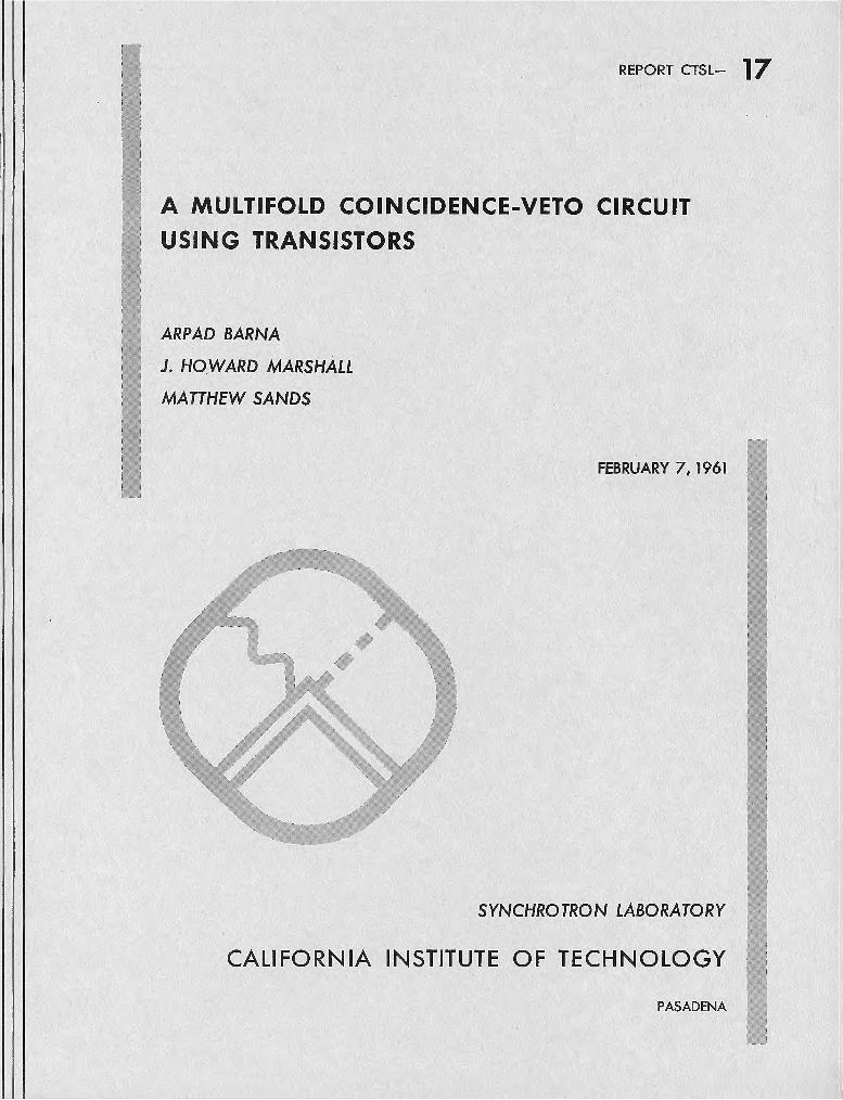
Fig. 1 shows the basic block diagram of the system.
The amplifier (Fig. 2) has a maximum gain of 250.
The triggering levels of the discriminators are adjustable from 1 to
10 volts. The outputs are 50 nsec wide negative pulses with 15 nsec rise-
time and 6 volt amplitude.
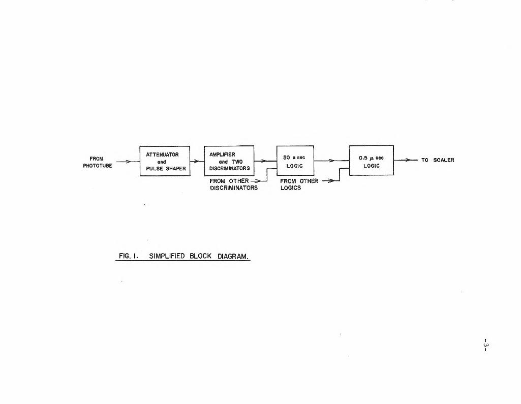
FIG. 1. SIMPLIFIED BLOCK DIAGRAM.
-3-
FIG. 2 . AMPLIFIER and DISCRIMINATOR.
-4-
-5-
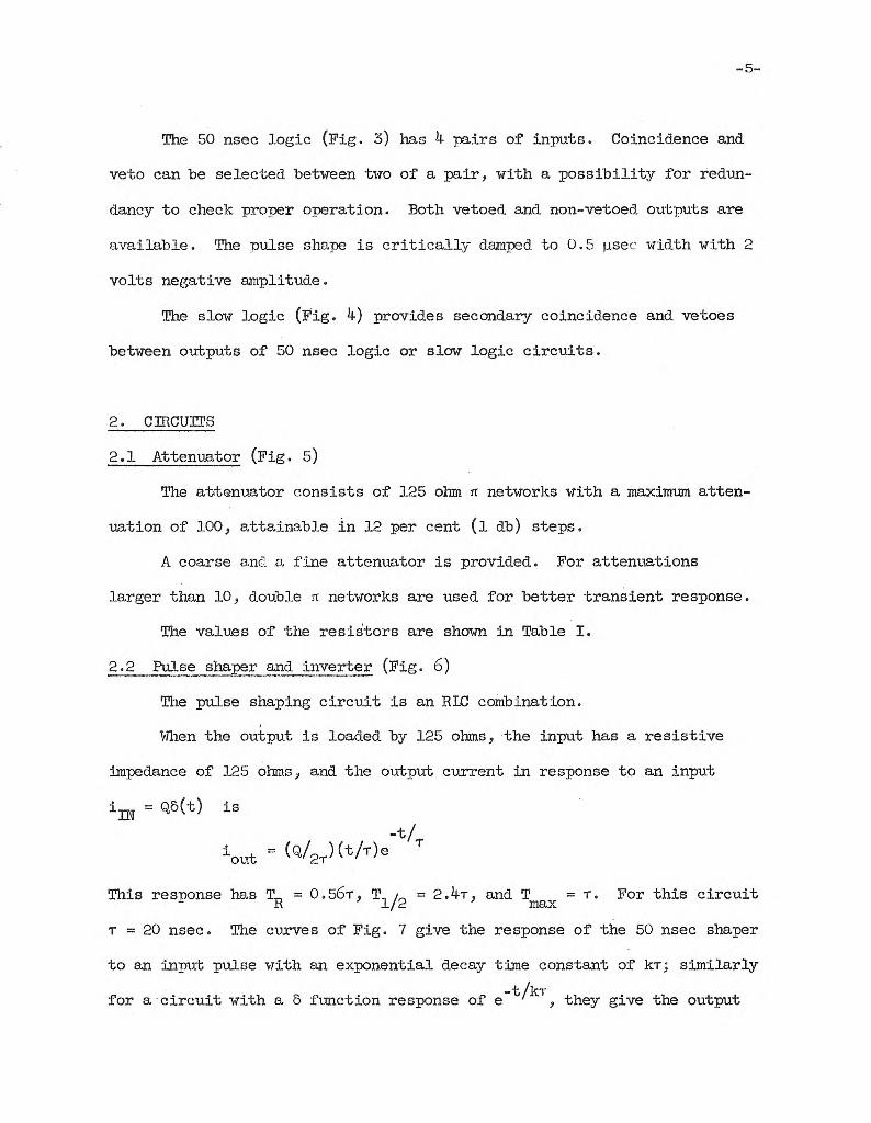
The 50 nsec logic (Fig. 3) has 4 pairs of inputs. Coincidence and
veto can he selected between two of a pair, with a possibility for redun
dancy to check proper operation. Both vetoed and non-vetoed outputs are
available. The pulse shape is critically damped to 0.5 μsec width with 2
volts negative amplitude.
The slow logic (Fig. 4) provides secondary coincidence and vetoes between outputs of 50 nsec logic or slow logic circuits.
2. CIRCUITS2.1 Attenuator (Fig. 5)
The attenuator consists of 125 ohm π networks with a maximum atten
uation of 100, attainable in 12 per cent (1 db) steps.
A coarse and a fine attenuator is provided. For attenuations
larger than 10, double π networks are used for better transient response.
The values of the resistors are shown in Table I.
2.2 Pulse shaper and inverter (Fig. 6)
The pulse shaping circuit is an RLC combination.
W hen the output is loaded by 125 ohms, the input has a resistive
impedance of 125 ohms, and the output current in response to an input
iIN = Qδ(t) is
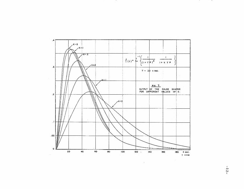
This response has Tr = 0.56τ, T1/2 = 2.4τ, and Tmax = τ. For this circuit
τ = 20 nsec. The curves of Fig. 7 give the response of the 50 nsec shaper
to an input pulse with an exponential decay time constant of kτ; similarly
for a circuit with a δ function response of e-t/kτ, they give the output

F IG. 3 . 50 n sec LOGIC
-6-

FIG. 4. 0.5 μ sec LOGIC.
-7 -

FIG. 5. ATTENUATOR.
-8-
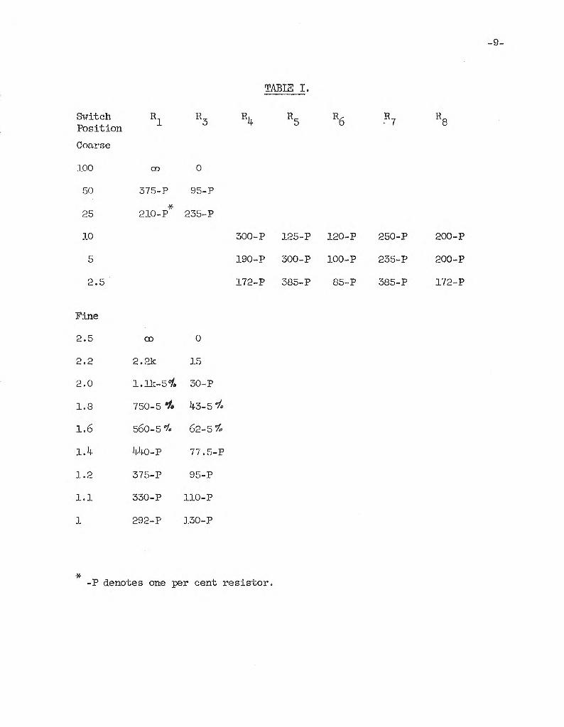
-9-
SwitchPosition R1 R3 R4 R5 R6 R7 R8
Coarse
100 ∞ 0
50 375-P 95-P
25 210-P* 235-P
10 300-P 125-P 120-P 250-P 200-P
5 190-P 300-P 100-P 235-P 200-P
2.5 172-P 385-Ρ 85-P 385-P 172-P
Fine
2.5 OD 0
2.2 2.2k 15
2.0 1.1k-5% 30-P
1.8 750-5 % 43-5 %
1.6 560-5 % 62-5%
1.4 440-P 77.5-P
1.2 375-P 95-P
1 . 1 330-P 110-P
1 292-P 130-P
*-P denotes one per cent resistor.
TABLE I.
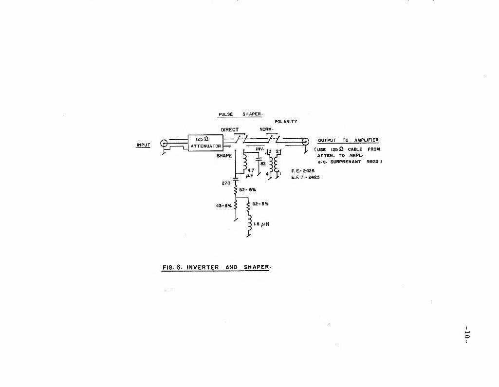
FIG. 6. IN V E R T E R AND SH A P ER .
-1
0-

-11-
for a 50 nsec shaper pulse.
The curves of Fig. 8 are derived from Fig. 7 and show the dependence
of the delay, rise time and amplitude loss on the exponential time con
stant.
Since the amplifier rise time is not stabilized by feedback, it is
not desirable for the output amplitude to be strongly dependent on the
amplifier rise time. The curves in Figs. 7 and 8 with k = 0.25
(kƬ = 5 nsec) approximately give the effect of the amplifier rise time
(10 per cent to 90 per cent ≈ 11 nsec) on the pulse shape. For this use
the amplitude loss at the peak is about 5 per cent, and thus ± 20 per cent
variations in amplifier rise time will produce a ± 1 per cent effect on
the peak amplitude.
The finite rise time also causes timing jitter for different input
pulse heights. For kr = 5 nsec (ΤR = 11 nsec) the peak of the pulse occurs
at 27 nsec, limiting the timing jitter to a maximum of 27 nsec. For the
same reason wide input pulses should not be used with the shaper. Photo
multiplier tube pulses with a half-width of about 10 nsec correspond to a
k of approximately 0.3, and thus produce an acceptable response. For 10
nsec wide input pulses, maximum timing jitter on the output of the dis
criminator was found to he 30 nsec. This limits the coincidence resolving
time to longer than 30 nsec.
The inverter consists of a 1:1 pulse transformer (PE-2425). The
transformer can be switched in or out of the signal path. For a 125 ohm
load, it has a 4 nsec rise time and 3 per cent droop at 50 nsec.
-12-
OUTPUT OF THE PULSE SHAPER FOR DIFFERENT VALUES OF K.
FIG. 7.

-13
-
FIG. 8.PULSE SHAPER DELAY, RISE TIME AND AMPLITUDE LOSS AS FUNCTION OF KƬ

- 14-
2.3 Amplifier (Fig. 9)
The amplifier consists of two stages, with a total gain of 250.
For large input signals the first stage can be bypassed and the output
stage, which has a gain of 5, can be used alone. The transient response
is adjusted so that, with an input pulse with a 12 nsec rise time, the
rise time of the output pulse is typically 17 nsec for a gain of 250, 15
nsec for a gain of 5; with overshoots and ringing less than 5 per cent.
The absolute value of the gain is within ± 5 per cent of the nominal
value, the linearity better than ± 1 per cent, for output pulse heights
< 10v . The input impedance is 125 ohms ± 5 per cent. The output impe-
dance < 15 ohms; the maximum duty cycle is 10 per cent. The temperature
drift of the amplification is less than ± 1 per cent for a temperature
change of ± 10°C. The operation is as follows:
First stage:
With the amplification switch in the 250 position, T1, T2, and T3
form a current feedback amplifier with a feedback current gain of 50.
T2 and T3 each give a current gain of β1). T1 isolates the output from
the input, preventing back interaction and, since it is a grounded base
stage, it has a current gain of α. The emitter of T2 is capacitively
grounded, making it a grounded emitter stage for signals. The coupling,
capacitor 0.01 µ from the collector of T2 to the base of T3 is chosen to
1) Symbols and equivalent circuits are discussed in: A. Barna, J. H.
Marshall, M. Sands: Nuclear Instruments and Methods 7 (1960) 124-134.
-15-
FIG. 9. AMPLIFIER.

-16-
give a closed loop decay time constant greater than 100 μsec. The signal
emitter current of T3 then divides between the 5 Ω to ground and the
264 Ω back to the emitter of T1. Thus, the open loop gain is
Mo ≅ α1β2β3 = 1200 and the feedback gain:
where RF = resistor from e1 to e3 = 264 Ω and RL is the resistor from e3
to ground (5 Ω). This gives a feedback factor F = Mo/Mf = 24 and an input
impedance to the emitter of T1 of re/F ≈ 0.2 Ω for times longer than
20 nsec. Thus, for the total input impedance one has RIN = 120 Ω, and
the long time response is determined by the 0.01 capacitor at the input.
Capacitor C1 is set for optimum transient response. The rise time can be
estimated:
where Ƭo = Ƭβ/β ≅ 0.5 nsec, Ƭβ is the β time constant, With the amplification switch in the 5 position, the signal is fed
into the emitter of T3 whose base has now been grounded to eliminate T1
and T2 from the loop. The 5 Ω resistor is disconnected from ground to
prevent its loading the input. T3 then has a current gain of α3 which is
nearly 1(~ 98 per cent) and an input impedance of the order of 1 Ω.
Second stage:
T4 acts as an isolation stage between the first stage and T5, and
it presents a low impedance to the collector of T3 and a high impedance
-17-
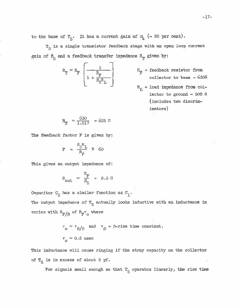
to the base of T5 . It has a current gain of α4 (~ 98 per cent).T5 is a single transistor feedback stage with an open loop current
gain of β5 and a feedback transfer impedance RT given by:
RF = feedback resistor from collector to base = 630 Ω
RL = load impedance from collector to ground ~ 500 Ω (includes two discriminators)
RT ≈ 630/1.017 = 625 Ω
The feedback factor F is given by:
F = β5RL/RF ≅ 60
This gives an output impedance of:
Rout ≈ RF/β5 = 8.5 Ω
Capacitor C2 has a similar function as C1.
The output impedance of T5 actually looks inductive with an inductance in
series with RF/β of RFƬ0 where
Ƭo ≈ Ƭβ/β and Ƭβ = β-rise time constant.
Ƭ0 ≈ 0.5 nsec
This inductance will cause ringing if the stray capacity on the collector
of T5 is in excess of about 5 pf.
For signals small enough so that T5 operates linearly, the rise time

-18-
of the second stage can be estimated as being:
where Cc = collector to base capacity of the transistor T5.
For Cc + C2 = 5 pf:
The DC currents through T1 and T2 are stabilized with emitter re
sistors; the emitter of T2 is by-passed to ground capacitively so as to
make it a grounded emitter stage for fast signals. The current through
T5 is stabilized by D.C. feedback from the collector to the base.
With the amplification switch in the 250 position, the current and
dissipation of T3 and T4 are stabilized by D.C. feedback from the collec
tor of T4 to the base of T3. The voltage of the base of T4 is determined
by a voltage dividing chain from the collector of T4 to the base of T3.
The emitter of T3 is essentially grounded through the 5 Ω resistor. In
the amplification = 5 position, the current is stabilized by the 2K and
2.5K resistors in the emitter of T3. The D.C. feedback is disconnected
by grounding the base of T3. The base voltage of T4 is derived from a
voltage divider chain as before.
All diodes (IN99) in the amplifier are protective.
2.4 Discriminator (Fig. 10)
The discriminator has a minimum useful input range of 1 to 10 volts
with a linearity better than 0.1 v . The change in triggering level for
constant amplitude pulses having widths of 20 ns and 200 ns is < 10mV;
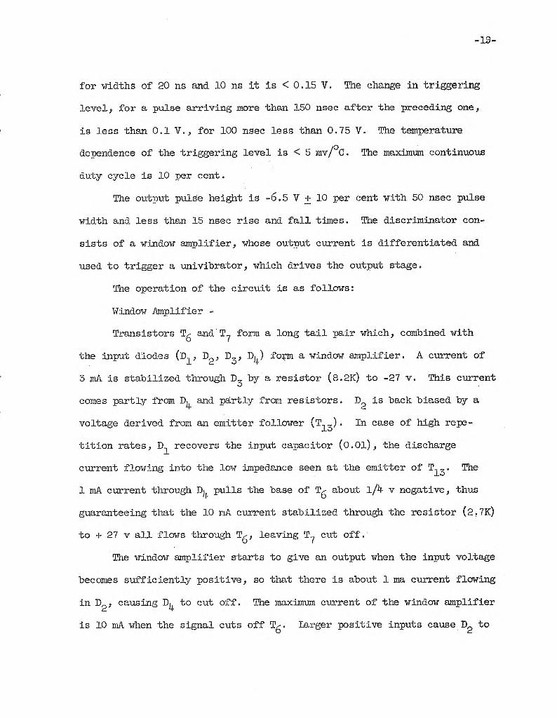
-19-
for widths of 20 ns and 10 ns it is < 0.15 V. The change in triggering
level, for a pulse arriving more than 150 nsec after the preceding one,
is less than 0.1 V., for 100 nsec less than 0.75 V. The temperature
dependence of the triggering level is < 5 mv/°C. The maximum continuous
duty cycle is 10 per cent.
The output pulse height is -6.5 V ± 10 per cent with 50 nsec pulse
width and less than 15 nsec rise and fall times. The discriminator con
sists of a window amplifier, whose output current is differentiated and
used to trigger a univibrator, which drives the output stage.
The operation of the circuit is as follows:
Window Amplifier -
Transistors T6 and T7 form a long tail pair which, combined with
the input diodes (D1, D2, D3, D4) form a window amplifier. A current of
3 mA is stabilized through D3 by a resistor (8.2K) to -27 v . This current
comes partly from D4 and partly from resistors. D2 is back biased by a
voltage derived from an emitter follower (T13). In case of high repe
tition rates, D1 recovers the input capacitor (0 .01), the discharge
current flowing into the low impedance seen at the emitter of T13. The
1 mA current through D4 pulls the base of T6 about 1/4 v negative, thus
guaranteeing that the 10 mA current stabilized through the resistor (2.7K)
to + 27 v all flows through T6, leaving T7 cut off.
The window amplifier starts to give an output when the input voltage
becomes sufficiently positive, so that there is about 1 ma current flowing
in D2, causing D4 to cut off. The maximum current of the window amplifier
is 10 mA when the signal cuts off T6 . larger positive inputs cause D2 to

-20-
F IG. 10. D ISC R IM IN A TOR.
-21-
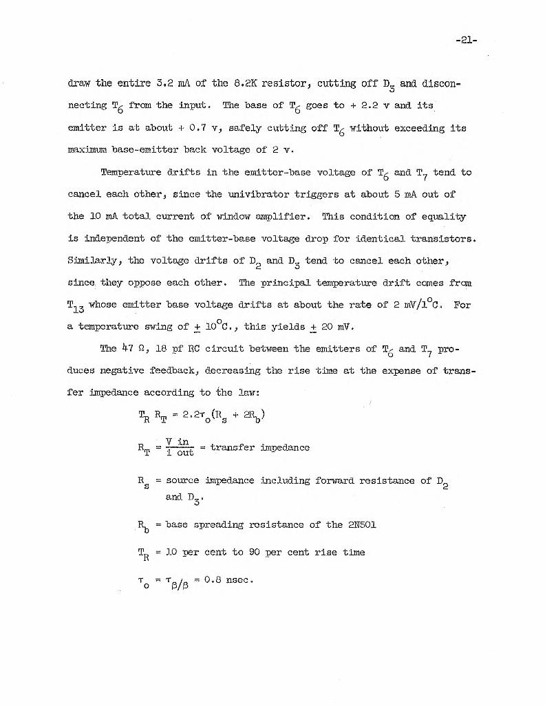
draw the entire 3,2 mA of the 8.2K resistor, cutting off D3 and disconnecting T6 from the input. The base of T6 goes to + 2.2 v and its
emitter is at about + 0.7 v , safely cutting off T6 without exceeding its
maximum base-emitter back voltage of 2 v .
Temperature drifts in the emitter-base voltage of T6 and T7 tend to
cancel each other, since the univibrator triggers at about 5 mA out of
the 10 mA total current of window amplifier. This condition of equality
is independent of the emitter-base voltage drop for identical transistors.
Similarly, the voltage drifts of D2 and D3 tend to cancel each other,
since they oppose each other. The principal temperature drift comes from
T1 3 whose emitter base voltage drifts at about the rate of 2 mV/l°C. For
a temperature swing of ± 10°C., this yields ± 20 mV.
The 47 Ω, 18 pf RC circuit between the emitters of T6 and T7 pro
duces negative feedback, decreasing the rise time at the expense of trans
fer impedance according to the law:
TR RT = 2.2Ƭo(Rs + 2Rb)
RT = V in / i out = transfer impedance
Rs = source impedance including forward resistance of D2 and D3.
Rb = base spreading resistance of the 2N501
Tr = 10 per cent to 90 per cent rise time
Ƭo = Ƭβ/β = 0.8 nsec.

-22-
The circuit used has a transfer impedance of about 70 Ω and TR ~ 10 nsec.
The fast rise time is necessary to reduce the pulse width dependence of
the triggering level.
Pulse Shaper -
The output of the window amplifier is shaped by the 10 μΗ choke and
the 39 pF capacitor. Diode D5 is normally slightly conducting and a low
impedance path exists through D5 and D6 to A.C. ground. Under these con
ditions the LC circuit is undamped and has a sinusoidal response with a
period of 70-80 nsec. When the signal current through the 39 pF condenser
reverses sign, it cuts off D5, leaving an impedance of 1.2K to ground,
which is large enough to overdamp the response of the LC circuit, causing
it to decay exponentially back to its D.C. level. Also, diode D5 dis
connects the trigger pulse from the univibrator after 35 nsec, allowing
the univibrator's pulse width to be independent of the input pulse width
even for long input pulses.
The damping of the pulse shaper response is critically dependent on
stray capacity across the 10 μΗ choke. In order to reduce this effect,
the choke is bypassed by 4.7K, providing additional damping.Univibrator -
Transistors T8 and T9 form a long tail pair with positive feedback
from the collector of T9 to the base of T8, making a univibrator. A
current of 4.6 mA is drawn through D6 causing T8 to conduct all of the 10.6 mA with T9 cut off. D8 is conducting a current of about 1 mA.
The circuit triggers when a trigger pulse greater than 4.6 mA unhooks D6 and causes current to flow in T9. For short times the 20 μΗ

-23-
presents a large impedance, and all of T9 's current flows back to the base of T8. This positive feedback continues to increase the current of
T9 until T8 cuts off. The base of T8 is clamped by D7 and a low impedance
path exists from the 500 Ω resistor to A.C. ground through D7 and D8.
The 20 μH choke, 500 Ω resistor, and 27 pF condenser form a critically
damped network causing the current through D7 to decrease with time.
After about 22 nsec, the current through D7 reaches zero, causing it to
unhook, leaving about 1.2K impedance to ground. The 20 μΗ choke con
tinues discharging through this impedance for another 5 nsec, at the end
of which time D6 starts conducting and T8 starts taking current from T9.
Thus, the circuit starts to trigger back in about 27 nsec. Since the
circuit has a rise and fall time of about 10 nsec, this gives a total
width at half maximum current (i.e., 5 mA) of:
Tl/2 = 1/2 (10 + 10) + 27 = 37 nsec
After the circuit triggers back, D8 unhooks the choke (20 μΗ),
recovers through a 2K resistance and disconnects all but about 1 mA of
its current from the biasing diode D7. The higher impedance causes the
choke to recover faster, and the fact that its current is no longer
flowing in D7 allows the circuit to be immediately retriggered. After
1 0 0 nsec, the choke is recovered and D8 starts conducting again and the
univibrator operates normally. For a trigger pulse less than 100 nsec
after the first triggering pulse, the circuit will retrigger, but its
pulse width is too short, due to residual current still flowing in the
choke.

- 24-
Output Stage -
Transistor T10 is normally cut off by the forward voltage drop of
D9 with its emitter clamped at 0.4 v by D10. When the univibrator is
triggered, the 10.6 mA from the collector of T8 is turned off, causing
the base of T10 to be pulled to -27 v through the 3.9k resistor. This
unhooks D10 and the emitter follows the base toward -27 v and stops at
-6.1 v when the transistor (T10) saturates. The fact that T10 saturates
causes its storage time to be added to the half width of the output pulse.
The storage time is specified as 13 nsec for the 2N501, resulting in:
T 1/2 = 37 + 13 = 50 nsecoutput
The rise time can be estimated as follows, for times short compared
to τβ = 40 nsec.
tR ≈ τo3 √(6CV/I oτo) = 11 nsec
where C = load capacity (370 pF for four logic circuits and connecting
cable).
V = output voltage (6.5 v)
Io = input current (7 mA)
τo = τβ/β = 0.8 nsecIf one includes a 10 nsec rise time for the input current:
Tr ≈ √((11)2 + (10)2) = 15 nsec

-25-
2.5 50 nsec logic (Fig. 11)
The logic is a fourfold coincidence circuit with four veto inputs.
There are two outputs, one for coincidence with veto and the other for
coincidence without veto. The coincidence resolving time is 37 ± 5 nsec,
the veto resolving time is 50 to 75 nsec, both defined as half width of
the delay curve at half height.
The output pulse is a critically damped -2.2 V ± 15 per cent pulse
with a width of 0.4 to 0.5 μsec at half height and the peak at 0.2 μsec.
The output for vetoed coincidence is typically ± 20 mv. The maximum con
tinuous counting rate is 1 mc. The output impedance is < 20 ohms, and
the output should not be loaded by more capacity than 300 pF.
The operation of the circuit is as follows:
Coincidence circuit -
The coincidence circuit is primarily an "And" circuit requiring the
presence of certain pre-selected inputs in order to get an output.
The transistor T1 is cut off by the forward voltage drop of
D1(Q 3-100). The D.C. current in D1 is determined by the coincidence
selector switch and the 4.2 mA drawn through resistors (7.5k-P, 51k-5
per cent) to -27 v . Whenever a coincidence selector switch is in either
a "U" or an "L" position (i.e., not off), it causes 5.2 mA to flow from
+ 27 v through the coincidence control diode (Dc-S570G). Of the total
current flowing through the eight Dc diodes, all but 4.2 mA normally
flows through D1. Thus, there can he from 1 mA (for only one coincidence
selector switch not off) to 16.6 mA (for no switches off) flowing in this
diode. In the case where all switches are off, the 4.2 mA pulls T1 into

-26-
FIG. 11. 50n SEC. LOGIC.

-27-
saturation.
When a Dc diode is connected to + 27 v through 5k by the coincidence
selector switch, thus conducting 5.2 mA, it can be cut off by a negative
signal which will absorb its 5.2 mA. The cathode of the Dc diodes
(i.e., base of T1) shifts only about 0.6 v from D1, conducting 17 mA to
T1 saturated. Thus, the required voltage at the input to cut off a Dc
diode is approximately 560 Ω x 5.2 mA = 3 v . When a Dc diode is not
connected to + 27 v through 5k by the coincidence selector switch, its
anode is pulled to -6 v by a resistor (57k) to -6.3 v . Thus, any nega
tive signals at its anode have little effect on the base of T1 . (It would
take a positive stray signal of + 6 v to turn the diode on.)
To turn on T1, D1 must cut off and the 4.2 mA current then pulls
T1 into saturation. This can happen only if all the Dc diode currents
are simultaneously zero. This means that one gets an output only if
there are simultaneous signals of at least -3 v on all inputs which are
connected to + 27 v through 5k by their coincidence selector switches.
Thus, one has provision for making one to four-fold coincidence, depending
on the setting of the coincidence selector switches.
When T1 saturates, it sends a current of 30 mA toward the base of
T2, cutting off D4 and saturating T2 . T1 also sends a 30 mA current
through the 50 nsec delay line toward the base of T5, unhooking D5 and
saturating T5 if there is no veto.
Veto Circuit (T4) -
The veto circuit is primarily an "Or" circuit which vetoes one of
the outputs of the coincidence circuit when any of certain preselected

-28-
inputs are present.
When no inputs are present, D2 and D3 are normally conducting,
holding the base of T4 at -5.2 v and thus cutting it off. If D2 should
become cut off, the 1.1 mA flowing through the resistor (20k) to -27 v
then pulls T4 into conduction, causing about 50 mA to flow through D5 and
its cathode to drop to about -6.9 v . If a coincidence current pulse of
30 mA arrives, it cannot unhook D5 and thus T5 does not turn on. The
(low) impedance of the voltage divider in the collector of T4 is chosen
so that the D.C. saturation current of T4 is greater than 30 mA, prevent
ing a loss of veto from pile-up on the collector of T4 .
When the veto selector switch connects the cathode of one of the
Dv2 diodes to -5.5 v, this pulls the cathode of the Dv1 diode connected
to it to -5.2 v and turns this diode slightly on. If a negative pulse is
applied to the cathode of such a conducting Dv1, then the diode conducts
harder, pulling the condenser (27 pF) on the anode of D2 down to nearly
the input voltage. This unhooks D2 and starts the veto procedure. When
the input signal returns to zero, the anode of Dv1 is held at about -11 v
for a -6 v input signal, while the cathode goes back to -5.2 v . Thus,
Dv1 cuts off and the 27 pF starts to decay exponentially to + 27 v with
a time constant given by 20k x 27 pF = 540 nsec. When the anode voltage
of D2 has reached -6.9 v, D2 starts conducting again, unclamping T1 and
ending the veto. The diode Dv2 presents a low impedance path for posi-
tive signals and thus recovers the input 1K condenser for pile-up at high
counting rates.
When the cathode of a Dv2 diode is left open by the veto selector

-29-
switch, then its anode is pulled to + 2 v , thus cutting off the Dv1 con
nected to this input. This blocks input pulses up to -7 v from operating
the veto circuit.
Output Circuit (T2T3T5T6) -
The purpose of the output circuit is to convert the short, fast
rise pulse from the output of the coincidence circuit (collector of T1)
into a longer, slow rise output pulse useful for driving scalers or the
Slow Logic.
The part of the circuit containing T2 and T3 is identical with the
part of the circuit containing T5 and T6 except for the veto transistor
T4 . If there is no veto, the outputs of the two parts are the same, and
if a veto is present, T3 gives the same output as if no veto were present,
but T6 gives no output.
Normally T2 and T5 are cut off by the forward voltages of D4 and
D5 respectively. These diodes draw 4 mA determined by resistors (5.1k)
to -27 v . In the collectors of T2 and T5 are pulse shaping networks
which convert a short voltage pulse into an output of the form
V(t) = Vo t/τe-t/τ where τ = 200 nsec. T3 and T6 are emitter followers
to prevent load impedances as low as 100 Ω from interfering with the pulse
shaping network. The narrow voltage pulse to drive this network is manu
factured by saturating T2 and T5 with the current coming from the satura
tion of T1 at coincidence. As the width of the pulse at the collector of
T1 changes from 10 nsec to 20 nsec, the output pulse amplitude changes
from 0.2 V to 2 V.
The pulse arriving at the vetoed coincidence output is delayed
-30-
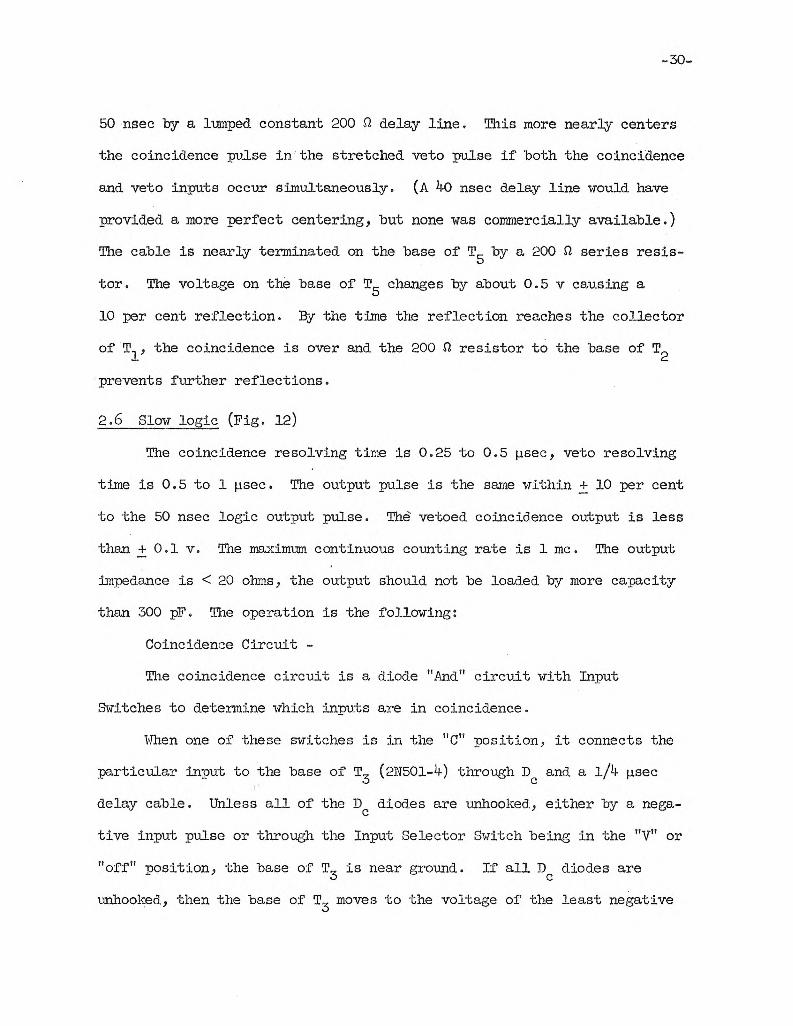
50 nsec by a lumped constant 200 Ω delay line. This more nearly centers
the coincidence pulse in the stretched veto pulse if both the coincidence
and veto inputs occur simultaneously. (A 40 nsec delay line would have
provided a more perfect centering, hut none was commercially available.)
The cable is nearly terminated on the base of T5 by a 200 Ω series resis
tor. The voltage on the base of T5 changes by about 0.5 v causing a
10 per cent reflection. By the time the reflection reaches the collector
of T1, the coincidence is over and the 200 Ω resistor to the base of T2
prevents further reflections.
2.6 Slow logic (Fig. 12)
The coincidence resolving time is 0.25 to 0.5 μsec, veto resolving
time is 0.5 to 1 μsec. The output pulse is the same within ± 10 per cent
to the 50 nsec logic output pulse. The vetoed coincidence output is less
than ± 0.1 v . The maximum continuous counting rate is 1 mc. The output
impedance is < 20 ohms, the output should not be loaded by more capacity
than 300 pF. The operation is the following:
Coincidence Circuit -
The coincidence circuit is a diode "And" circuit with Input
Switches to determine which inputs are in coincidence.
When one of these switches is in the "C" position, it connects the
particular input to the base of T3 (2N501-4) through Dc and a l/4 μsec
delay cable. Unless all of the Dc diodes are unhooked, either by a nega
tive input pulse or through the Input Selector Switch being in the "V" or
"off" position, the base of T3 is near ground. If all Dc diodes are
unhooked, then the base of T3 moves to the voltage of the least negative
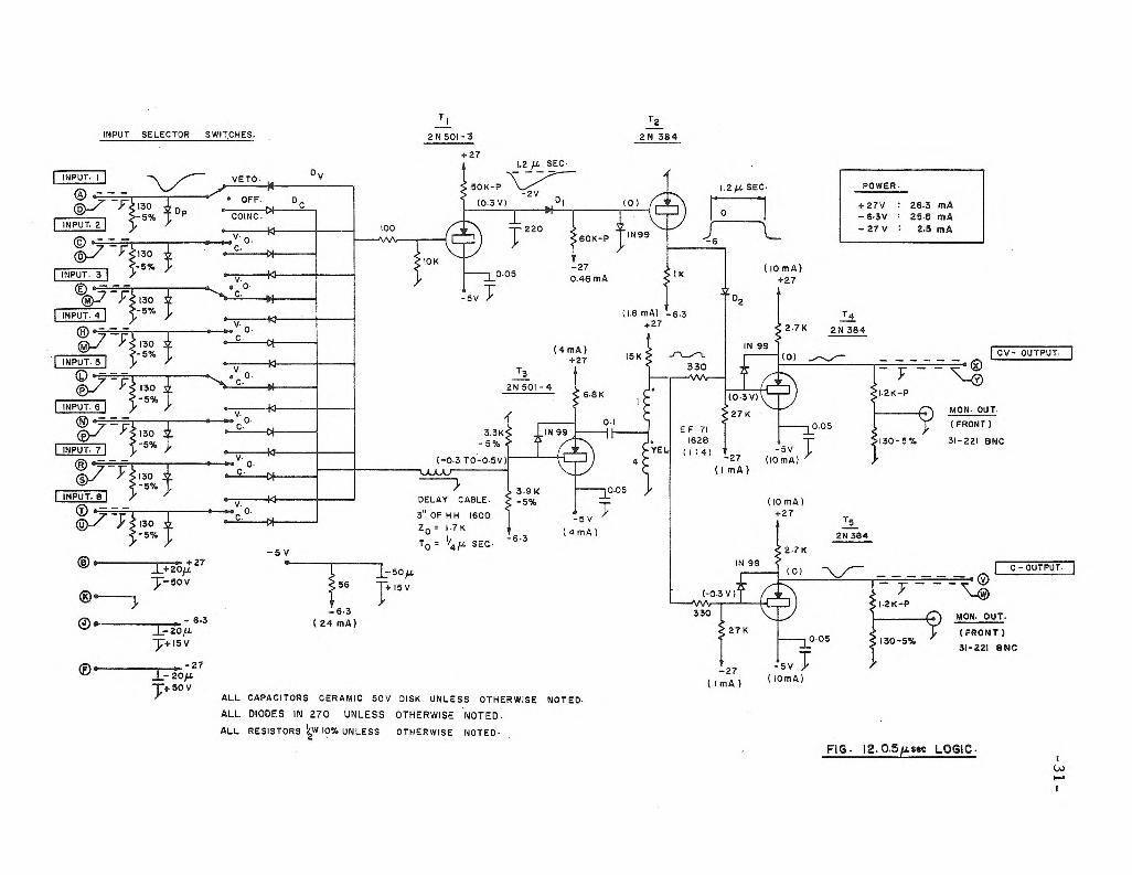
FIG. 12. 0.5μsec LOGIC. -31
-

-32-
input to -3 v, whichever is less negative.
Transistor T3 is an emitter follower and drives the 1:4 transformer
(EF71-1628) which is connected as an auto transformer giving a 25 per cent
voltage increase. The purpose of this transformer is to make up voltage
losses in the emitter followers and thus give nearly unit gain from the
input to the output at coincidence. This makes it possible to cascade
slow logic circuits.
The 1 / 4 μsec delay cable (HH l600) delays the coincidence inputs
with respect to the veto inputs so that the veto pulse will overlap the
coincidence pulse. The delay line is terminated in 1.7K at the base of
T3.The diodes Dp on the input are to recover the capacitors coupling
the outputs of the Logic Chassis. This prevents large D.C. drifts on the
input at high counting rates. The IN99 diodes from emitter to base of the
transistors are all protective.
Veto Circuit (T1, T2) -
The veto circuit is a diode "Or" circuit with the Input Switches
determining which inputs can veto.
When one of these switches is in the "V" position, negative pulses
on its input will pass through diode Dv (IN270) and reach the base of T1.
This charges the stretching capacitor (220 pF) which holds D1 (IN270)
unhooked for 1 μsec after charging. When D1 is unhooked, the 1/2 mA
flowing in the 60K resistor pulls T2 (2N384) into saturation, raising its
collector voltage from -6.3 v to zero. This makes D2 (IN270) ready to
conduct and prevent the passage of negative signals to the base of T4
-33-
(2N384). Thus, the output of T4 is vetoed by the low impedance of the
saturated transistor T2.
Output Stages (T4, T5) -
Both the coincidence output stage (T5) and the vetoed coincidence
output stage (T4) are emitter followers. They are both connected to the
transformer (EF71-1628) by 330 Ω resistors, and the bases are pulled
negative by 1/3 v so as to give nearly zero output D.C. voltage.
The vetoed coincidence output stage is coupled by 330 Ω to the
transformer so that the delay line termination will not be significantly
changed by the low impedance seen at the base of T4 when a veto is pre
sent. For the same reason, T3 was chosen to be a high beta transistor
(β > 100). The 300 Ω was used in the coincidence output stage so that
the two output impedances would be the same when no veto was present.
The collectors of all the emitter followers are decoupled from the
-6.3 v supply by 56 Ω and 20 μF to prevent pickup from pulse loading of
the supply.
3. CONSTRUCTION
The circuits are built on 16 cm x 20 cm copper plates, having
4 cm x 17.5 cm front panels. Ten of these units plug into a 17.8 cm
x 45 cm rack. Signals as well as power lines connect through the rear
connector, the monitor coax connectors and the controls are mounted on
the front panel. Components are mounted on ceramic terminal strips with
coaxial cables and D.C. wires underneath. Care has been taken to keep
grounds short. Interconnections between the discriminators and 50 μsec
-34-
logic circuits use 50 ohm cable with taper pins; other signal wires
125 ohm cable. It was found necessary to provide low inductance grounds
to each chassis in a sliding contact built into the mounting channel.
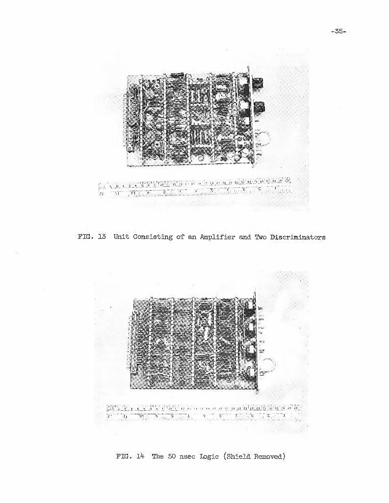
Fig. 13 shows the unit of an amplifier and two discriminators. The
first stage of the amplifier is located at the upper front part, the
second stage under it, the two discriminators in the rear part.
Fig. l4 shows the 50 nsec logic. The coincidence and veto diodes
are located in the rear and the 50 nsec lumped constant delay line at the
upper front part. Six attenuators, pulse shapers and inverters are
mounted on a 9 cm panel (Fig. 16).
4. PERFORMANCEThe circuit has been used successfully to identify protons and
pions in a six counter telescope at the Caltech synchrotron (Fig. 16).
At the present time, this telescope has been expanded to nine counters
with dE/dx windows set by this circuit aiding in the detection of 150 Mev
K+ mesons. Plans are being made to make a further expansion of the tele-
scope to 12 to 15 counters and detect higher energy K+. Experience in
the past has shown the circuit to have the high degree of stability and
reliability required for such multi-counter experiments demanding narrow
amplitude windows.
Extreme care has to be taken to provide reliable power lines
(+ 27 V, -27 V, -6.3 V), since the absence of any of them may cause
serious damage to the circuit. A safety interlock circuit has been used
to ensure simultaneous shorting of all lines, if one fails.
-35-
FIG. 13 Unit Consisting of an Amplifier and Two Discriminators
FIG. 14 The 50 nsec Logic (Shield Removed)

-36-
FIG. 15 The 0.5 μsec Logic and the Shield
FIG. 16 An Instrument as Incorporated Into an Experiment

