a mixed-signal demodulator for a low-complexity ir-uwb receiver: methodology, simulation and design
TRANSCRIPT

ARTICLE IN PRESS
INTEGRATION, the VLSI journal 42 (2009) 47–60
Contents lists available at ScienceDirect
INTEGRATION, the VLSI journal
0167-92
doi:10.1
� Corr
E-m
journal homepage: www.elsevier.com/locate/vlsi
A mixed-signal demodulator for a low-complexity IR-UWB receiver:Methodology, simulation and design
Marco Crepaldi �, Mario R. Casu, Mariagrazia Graziano, Maurizio Zamboni
Dipartimento di Elettronica, Politecnico di Torino, Corso Duca degli Abruzzi 24, 10129 Torino, Italy
a r t i c l e i n f o
Keywords:
UWB communications
Mixed-signal integrated circuits
Design methodology
Energy detection
2-PPM modulation
60/$ - see front matter & 2008 Elsevier B.V. A
016/j.vlsi.2008.07.005
esponding author. Tel.: +39 0115644004; fax:
ail address: [email protected] (M. Crep
a b s t r a c t
This works presents an integrated 0:18mm CMOS 2-PPM demodulator based on a switched capacitor
network for an energy detection impulse-radio UWB receiver. The circuit has been designed using a top-
down methodology that allows to discover the impact of low-level non-idealities on system-level
performance. Through the use of a mixed-signal simulation environment, performance figures have
been obtained which helped evaluate the influence at system level of the non-idealities of the most
critical block. Results show that the circuit allows the replacement of the ADC typically employed in
energy detection receivers and provides about infinite equivalent quantization resolution. The
demodulator achieves 190 pJ/bit at 1.8 V.
& 2008 Elsevier B.V. All rights reserved.
1. Introduction
The impulse-radio ultrawideband (IR-UWB) technology is apromising solution for short-range indoor applications. It isparticularly suited for applications aimed at connecting portabledevices in wireless private area networks (WPAN) and for low-powersensor networks with low-computational demands, reduced com-plexity transceivers and centralized control for multiple accesses.Generally, transceivers are designed to have high-bandwidth, low-peak powers at transmitters, low-complexity and the flexibility ofsupporting different data rates. The ‘‘carrier-less’’ transmission relieson short duration pulses which satisfy FCC spectral requirementsabout both ultra-wide bandwidth occupations and low-powerspectral densities (PSDs) [1]. Thanks to these features, IR-UWB isparticularly suited to low-power applications in which extendedbattery lives are a fundamental requirement [2].
For this kind of applications, low-complexity architecturesmust be employed in UWB receivers. Typically two approachesare used: the coherent and the non-coherent ones. The firstperform demodulation by correlating the incoming UWB pulseswith an internally generated waveform template. The second donot make any attempt to calculate the correlation of the incomingpulse, and perform demodulation without any a priori informa-tion regarding the channel. The non-coherent receivers permitlower-power consumption and lower-complexities than in coher-ent receivers with a slight penalty in the bit-error-rate (BER). Thisdrawback is overcome in short-range applications in whichthe possibility of saving energy at the receiver side dominates
ll rights reserved.
+39 0115644099.
aldi).
the performance loss and the power budget at the transmitter. Forlow-data rates coherent receivers generally have an energy perbit 10 times higher than for non-coherent receivers [3]. Amongthe various non-coherent alternatives, the energy detection (ED)approach is particularly interesting. Notwithstanding the 3 dB lossin the BER with respect to coherent receivers, the UWB modulatedinformation is simply recovered by evaluating the received pulsesenergy. Due to the nature of ED schemes, receivers are insensitiveto phase dependent modulations, thus data are transmittedaccording to time-based modulation schemes. Their low-powerconsumption is appealing in battery-powered short-range appli-cations, in which full CMOS integration plays a crucial role for theoverall device cost.
In typical implementations of ED receivers, energy is calcu-lated after signal rectification by using integrate-and-dump (I&D)units. Such units, realized as open loop Gm � C integrators forachieving large bandwidths [4], are typically followed by ananalog-to-digital converter (ADC) and by a digital back-end thatpermits demodulation. Performance is affected by the ADCresolution and the features of the integrator unit; in additionto this, the ADC represents one of the most power-hungry andsilicon area-consuming blocks [5]. Since IR-UWB communicationsystems operate by means of time-domain modulations, it ispossible to use ad hoc solutions by reorganizing the generalarchitectures thus eliminating the ADC and allowing low-powerconsumption. In the case of 2-PPM modulations, it is possible toreplace the analog-to-digital conversion stage with simpler blockswhich allow to compare the pulses energies in the analog domain[6,7], therefore avoiding any quantization effect. With the aim of alow-power receiver and using a single comparator as in [6], thiswork presents an integrated differential 2-PPM CMOS demodu-lator formed by an open-loop Gm � C structure, called bi-phase

ARTICLE IN PRESS
m(t)2
>
t
m(t)
t
IRP
’1’’0’
0/1
∫
∫
PIR
Fig. 2. 2-PPM modulation.
M. Crepaldi et al. / INTEGRATION, the VLSI journal 42 (2009) 47–6048
integrator. It inherently provides analog-to-digital conversionwithout the use of any ADC, features offset rejection and exhibitsnearly the same error-rate performance of an ideal ED receiver.The demodulator is composed of an operational transconductanceamplifier (OTA) and a differential switched capacitor network.The demodulator consumes 950mW and achieves 190 pJ/bit at5 Mbit/s.
The design and the simulation of the entire unit have beencarried out with a design methodology based on differentabstraction levels, the development of a proper VHDL-AMSsimulation environment and the use of a mixed-signal simulationtool, ADVanceMS (ADMS, Mentor Graphics). Description levelswith different degrees of accuracy allow to discover the impact ofthe abstraction refinement, thus help the designer trade betweenprecision and simulation time [8]. For the low-level descriptions,the circuit building blocks have been designed in a mixed-modeUMC CMOS 0:18mm technology and simulated with SPICE BSIM3transistor models. The design methodology combined withthe simulation tool allowed to discover design weaknesses thushelping us to accurately predict performance in presence of blocksnon-idealities.
The paper is organized in the following parts: Section 2introduces the principle of operation of the reduced complexityED receiver which employs the bi-phase demodulator, andhighlights its differences with respect to the ordinary EDreceivers. Section 3 introduces the successive refinement stepdesign methodology. Section 4 introduces the bi-phase demodu-lator unit and its main building blocks—the integrator and thecomparator—explains the typical design issues and clarifiesthe trade-off between performance and low-power consumption.In addition, the section justifies the abstraction level required forsimulating each of the two units. Section 5 reports both functionaland system-level performance simulations. Finally, conclusionsare drawn in Section 6.
2. Low-complexity ED receiver
IR-UWB transmission is based on the use of short durationbaseband pulses, on the order of 1 ns, without the need of anycarrier to provide bandwidth shifts. The PSD is very low withrespect to narrowband and wideband modulations but the totaltransmitted power can be considerably high because of the veryhigh-bandwidth. The baseband pulses are phase-modulated, likein bi-phase shift keying (BPSK), or time-modulated, like in pulseposition modulation (PPM).
Typical impulse-radio ED receivers front-ends include a low-noise-amplifier (LNA), a squaring unit (ðÞ2), an analog integratorand finally an A/D converter, as Fig. 1 shows. Sophisticatedoperations other than simple demodulation, like for instance thesynchronization, are typically done in the digital domain byelaborating the ADC output’s raw data.
A typical modulation scheme is the 2-PPM (bi-phase pulse-position-modulation) in which the transmitted pulse is modu-lated according to its relative position within a time frame, asshown in Fig. 2. Whether a ‘‘0’’ is sent, the pulse is placed in the
LNA ()2 I & DAntenna A/D
Fig. 1. Typical energy detection receiver.
first half of a pulse-repetition-interval (PRI), while in case of a ‘‘1’’,the pulse is placed in the second one. At the receiver, the UWBsignal, rectified by the squarer, is I&D in the two PRIs halves by theI&D unit. The two obtained analog values represent the signalenergies associated to the two PPM phases. After A/D conversion,data are demodulated by comparing the energies of the two PPMphases numerically.
With the intent of reducing complexity and power consumption,in this work we replace the ADC with a simple zero-thresholdcomparator by giving the analog integrator the capability to providea voltage whose sign determines the information bit. We call thisnew receiver as bi-phase demodulator and the reason of this namewill be clear momentarily. The circuit is based upon the chargeredistribution principle.
The bi-phase demodulator shown in Fig. 3 is composed of twoparts, the bi-phase integrator and the comparator. The bi-phaseintegrator recalls the typical Gm � C integrator structures: It iscomposed of an open loop transconductor loaded with a capacitorcontained in the integration network. After this first conditioningpart which generates a modulation-dependent analog voltage, theresult is processed by the zero-threshold comparator whichconverts the demodulation voltage into a binary digital quantity.
Differently from other works in which full receiver front-endsare presented, here the contribution is more focused on the designof a single unit of the demodulation chain and on how its non-idealities impact on system-level performance. With respect to[7], in which baseband processing relies on a single-endedinverter, here the demodulator is composed of a fully differentialOTA inclusive of common mode stabilization network. The circuitdescribed in detail in Section 4 is a mixed-signal device becausethe analog voltage processing in the integration network of Fig. 3is controlled by switching transistors. Therefore, to obtain theimpact at system level of a single block, a proper mixed-signaldesign methodology must be employed in the various designstages.
3. Design methodology
Hardware description languages like VHDL and Verilog aretypically employed in digital design. With the introduction ofVHDL-AMS, a superset of the VHDL language, it became possibleto employ both continuous-time and digital descriptions in thesame simulation, thus allowing true mixed-signal simulationsin which analog and digital parts are simulated concurrently.The design and the simulation of the bi-phase demodulator andof the receiver front-end need not only a proper language but alsoa design tool through which the description language can be‘‘brought to life’’. An example is ADVanceMS which can simulateboth VHDL-AMS and SPICE descriptions. Interesting examples ofthe use of VHDL-AMS and the ADMS tool are [9,10]. The languagecombined with the tool allows the designer to create an ad hocsimulation environment in which the system functionalities can

ARTICLE IN PRESS
Vota Vout
Iout
Ios+
Antenna ()2+
−
−
+OTA
Res
etPh
ase
0Ph
ase
1C
ompa
re
Inhi
bit
0/1Com
Vos+
Save
Cla
mpe
rLa
tch
IntegrationNetworkLNA
Bi−phase integrator
Bi−phase demodulator
comparator
Fig. 3. Energy detection receiver with bi-phase demodulator.
>LNA ( )2
( )2
( )2
Fully
beh
avio
ural
Subs
titut
e−an
d−pl
ayPh
ysic
al b
lock
sid
entif
icat
ion
LNA
P3−S P3−L
P1
P3−S
>LNA BP−I
BP−I
P2
Phas
e I
Phas
e II
Phas
e II
I
Fig. 4. Design flow phases using VHDL-AMS and ADMS.
M. Crepaldi et al. / INTEGRATION, the VLSI journal 42 (2009) 47–60 49
be tested. In addition, the possibility to use VHDL-AMS and SPICEdescription in the same environment allows to refine the blocksdescription from pure behavioral models down to circuitstructural descriptions (e.g. transistor-level). In other words, top-down methodologies typical of the digital design can be alsoapplied to the case of mixed-signal devices.
We adopted the design methodology outlined in [11] where weproposed a successive refinements-based approach. We tookadvantage of the inherent partitioning properties of the VHDL-AMS language, that is the possibility to assign each part of thedesign the description of its interface with the outer world, i.e. itsentity, and the description of the reaction of its inner parts tothe signals listed in the entity as well as to its internal states, i.e.its architecture. Our approach consists of three steps: Phase I—
Architectural description, Phase II—Partitioning and Phase III—
Substitute-and-play. In Fig. 4, the different block shapes in PhasesII and III identify the entity/architecture partitioning. The blocklabeled as BP-I indicates the bi-phase integrator.
During Phase I the general system architecture is conceived.This functional description does not necessarily assign each blockof the architecture a specific task but rather consider the systemas a whole. In addition it is also possible to prove the coherencewith other high-level languages such as Matlab [12].
During Phase II, the architecture is partitioned into singleblocks, each with a proper VHDL-AMS entity and architecture. It ispossible to partition the whole front-end in smaller units such asthe LNA, the squarer and the bi-phase demodulator. At this levelelectrical compatibility among the units must be provided. Eachunit has its own terminals which identify inputs, outputs andpower supply nets. The units are still behaviorally modeled butthe description is detailed enough to let the designer considerthe first macroscopic non-ideal parameters in the models, likesaturation, slew-rates, input and output impedances et cetera.Since the testbenches are inherited from Phase I, it is possible toevaluate the effect of these non-idealities on the systemperformance. It is then now possible to investigate on themacroscopic front-end requirements for a single block (e.g. gain,linearity, bandwidth) and to derive constraints for the successivecircuit-level design phases. In addition, it is possible to determinethe most critical blocks through simulated performance figures orelectrical-level considerations.
During Phase III, the description of one or more blocks isrefined. For example, the bi-phase integrator, that was describedin Phase II with VHDL-AMS equations, can be substituted with atransistor-level description. During this phase, the componentinstantiations are replaced without changing the upper levelVHDL-AMS source code. This ‘‘painless’’ substitution, we call itsubstitute-and-play, is allowed by the partitioning done in Phase IIsince electrical terminals do not change once defined (the blocksinterfaces, that is the ‘‘entities’’, are not modified). The substitu-tion operation can be applied also to a subset of the blocks the
designer considers relevant to understand its effect on the system.Typically, one or two blocks are replaced at time. Whetherthe layout-extracted SPICE netlist is available, or the effect ofparasitics is relevant for the system-level performance evaluation,the designer can import such low-level description of a blockin the simulation environment. Whether the results obtained inPhase III do not differ from those obtained during Phase II, it ispossible to simulate the system by using the simpler higher-levelmodel (and this will save simulation time) and to focus on therefinement of the front-end units which have not been consideredyet.
In the remainder of the paper we will use the followingnotation: P1—Conceptual Phase I, P2—Behavioral model—PhaseII, P3-S—SPICE level—Phase III, P3-L—Layout level—Phase III.
4. Integrated demodulator
4.1. Bi-phase integrator
This subsection introduces the bi-phase integrator unit. It isorganized in two parts: The first one deals with the principle ofoperation whereas the second one focuses on the transistor-leveldesign of the device.
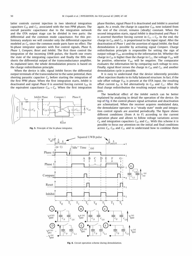
4.1.1. Principle of operation
Fig. 5 details the bi-phase integration network of Fig. 3. Theintegrator includes the transconductor, which consists of an OTA[13], and a switched capacitor network [14]. The former trans-forms the input voltage variations V in into current Iout, while the
ARTICLE IN PRESS
M. Crepaldi et al. / INTEGRATION, the VLSI journal 42 (2009) 47–6050
latter controls current injection in two identical integrationcapacitors CL0 and CL1 associated with the two PPM phases. Theoverall parasitic capacitance due to the integration networkand the OTA output stage can be divided in two parts: thedifferential and the common mode capacitance. For this pre-liminary analysis we will consider only the differential capacitormodeled as Cp since the common mode parts have no effect. Thebi-phase integrator operates with five control signals, Phase 0,Phase 1, Compare, Reset and Inhibit. The first three control theintegration of the incoming UWB pulses, the fourth one resetsthe state of the integrating capacitors and finally the fifth oneshorts the differential output of the transconductance amplifier.As explained later, the whole demodulation process is based onthe charge redistribution principle.
When the device is idle, signal Inhibit forces the differentialoutput terminals of the transconductor to the same potential, thenshorting parasitic capacitor Cp before starting the integration ofthe first PPM phase. When the first integration starts, Inhibit isdeactivated and signal Phase 0 is asserted forcing current Iout inthe equivalent capacitance CL0 þ Cp. When the first integration
Vota
Iout
OTA
+
−
VoutCp CL1CL0
Inhibit Phase
Reset
Phase 0Compare 1
Fig. 5. Principle of the bi-phase integrator.
B
i iT1T0 T0
Vfph0
A B C
(n−1) (n)
Squared UWB pV (t)in
‘‘Idle’’ Time
0Phase
Phase 1
Compare
C p C L0
C p C L1
Vp (n)fph1 C p
Vp (n)fph0 C p
+
+
Vp (n)iph0
TT
A
ED
Vp (n)iph1 =
= (n)
Reset
Inhibit
Fig. 6. Circuit operation schem
phase finishes, signal Phase 0 is deactivated and Inhibit is assertedagain. As a result, the charge in capacitor CL0, now isolated fromthe rest of the circuit, remains (ideally) constant. When thesecond integration starts, signal Inhibit is deactivated and Phase 1is asserted therefore forcing current in CL1 þ Cp. In the end, thecharge in CL0 and CL1 is proportional to the input signal: After thedeactivation of Phase 1 and the assertion of signal Inhibit, the finaldemodulation is possible by activating signal Compare. Chargeredistribution principle is responsible for setting the sign ofoutput voltage Vout according to the information bit. Whether thecharge in CL0 is higher than the charge in CL1, the voltage Vout willbe positive, otherwise Vout will be negative. The comparatorevaluates the information bit by comparing such voltage to zero.Finally, signal Reset zeroes the charge in CL0 and CL1 and anotherdemodulation cycle is possible.
It is easy to understand that the device inherently providesoffset rejection thanks to its fully balanced structure. In fact, if thesole offset voltage VOS is present at the OTA input, the resultingoffset current IOS is fed alternatively in CL0 and CL1: After thefinal charge redistribution the resulting output voltage is ideallyzero.
The beneficial effect of the Inhibit switch can be betterexplained by analyzing in detail the operation of the device. Ontop of Fig. 6 the control phases signal activation and deactivationare schematized. When the receiver acquires modulated data,the demodulator operates in a ‘‘steady state’’ mode and integra-tion control signals are asserted periodically. The figure showsdifferent conditions (from A to F) according to the currentoperation phase and allows to follow voltage variations acrossCp and integration capacitors CL0 and CL1. With this scheme it ispossible to focus our attention on the initial and final conditionsacross Cp, CL0 and CL1 and to understand how to combine them
i i1T
C
D E F G
ulse
t
t
t
t
G
t
+
+ C L1
C L0V (n)
out
Cp CV (n)
fph1L1CL1
Cp CL0CL0
++
++
Vfph0(n)
T T
F
t
t
e during demodulation.

ARTICLE IN PRESS
M. Crepaldi et al. / INTEGRATION, the VLSI journal 42 (2009) 47–60 51
together to obtain the mathematical expression representing theinfluence of parasitics on Vout. Condition G represents the finalcharge redistribution after having completed the two demodula-tion phases.
We define T i as the idle time between the deactivation of Phase
0 and the activation of Phase 1 and vice versa.In addition, we define the voltages Vp;ðnÞ
iph0, Vp;ðnÞ
fph0, Vp;ðnÞ
iph1, Vp;ðnÞ
fph0
across the capacitance Cp (superscript p), where n indicates thecurrent demodulation period. The equations state how the initialand final conditions on voltage across Cp impact on CL0 and CL1 atthe beginning and at the end of each demodulation phase.Subscripts i and f indicate the initial and final conditions across Cp
during the idle period, for Phase 0 (ph0) and Phase 1 (ph1)operation states, respectively.
To take into consideration the charge transfer it is alsonecessary to define the quantities V ðnÞiph0
, V ðnÞfph0, V ðnÞiph1
and V ðnÞfph1which
represent the voltages across both CL0 and CL1 during theactivation of the respective integration switches.
When signals Phases 0 and 1 are asserted, the OTA integratesthe UWB signal generating the information required for demodu-lation:
V ðnÞ0 ¼1
Cp þ CL0
ZT ðnÞ
0
GmV inðtÞ and V ðnÞ1 ¼1
Cp þ CL1
ZT ðnÞ
1
GmV inðtÞ
where T0 and T1 indicate the domains of integrations of equalduration for Phases 0 and 1, respectively.
With these hypotheses it is possible to obtain Eqs. (1)–(4)which model the operation of the device for the first of the twoPPM integrations at time n in case the Inhibit signal is not used:
Vp;ðnÞfph0¼
IOST i
Cpþ Vp;ðnÞ
iph0þ Np;ðnÞ
fph0(1)
V ðnÞiph0¼
Cp
Cp þ CL0Vp;ðnÞ
fph0(2)
V ðnÞfph0¼ V ðnÞiph0
þ V ðnÞ0 (3)
Vp;ðnÞiph1¼ V ðnÞfph0
(4)
For the second PPM phase, it is possible to obtain a similar set ofequations (not reported for sake of brevity). On activation of signalCompare, considering that the integration capacitors are equal(CL0 ¼ CL1 ¼ CL), the final output voltage after the final chargeredistribution is given by V ðnÞout ¼
12 fV
ðnÞfph1� V ðnÞfph0
g.If we combine the two sets we can express V ðnÞout as a function of
V ðn�1Þout :
V ðnÞout ¼1
2V ðnÞ1 �
CL
Cp þ CLV ðnÞ0
(þ
Cp
Cp þ CLfNp;ðnÞ
fph1� Np;ðnÞ
fph0� V ðn�1Þ
1 g
þC2
p
ðCp þ CLÞ2fV ðn�1Þ
out � Np;ðn�1Þfph1
þ Np;ðn�1Þfph0
g
)(5)
In the case in which no reset switches across Cp are employed, thedifferential output voltage for the n-th integration V ðnÞout dependson the stochastic processes Np
fph0and Np
fph1both for the n-th and
the ðn� 1Þ-th demodulation phase. If Cp is zero, it is easy todemonstrate that demodulation voltage is ideal, that is
V ðnÞout;ideal ¼12fVðnÞ1 � V ðnÞ0 g
To obtain a similar effect in presence of parasitics, it is sufficient toreset the charge accumulated in Cp before a new phase starts withsignal Inhibit. In this case, Vp;ðnÞ
iph0¼ Vp;ðnÞ
fph1¼ 0: That is, using the
reset switches across Cp, the obtained output voltage is ideal.In both cases, the equations presented show how the
symmetric structure of the circuit completely eliminates the
effect of offset contribution VOS. In fact, the final output voltagedoes not depend on current IOS. In summary, the possibilityof resetting charge in Cp before starting a new demodulation andthe offset rejection capabilities allows to obtain almost idealdemodulation performance.
4.1.2. Design
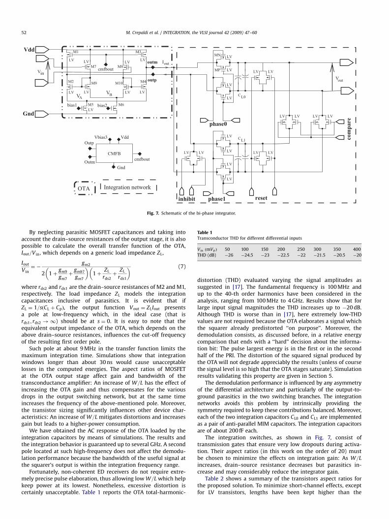
Fig. 7 presents the overall schematic of the bi-phase integrator.It shows the internal OTA structure and the integration network.The circuit is fully differential and the OTA input stage consistsof a source-follower differential configuration. Current variationsat the input are mirrored in the output stage through a MOSFETconfiguration similar to a current mirror. The technologyemployed here is a mixed-mode CMOS 0:18mm process. Forenhancing the over-drive of some of the transistors, the low-threshold voltage (LV) process option has been employed.
The amplifier includes auto-biasing circuits and a simplecommon mode feedback network (CMFB) made up of a differ-ential stage only. On the one hand, as clarified in [15], the use of acommon mode stabilization network is mandatory for integratorsemploying open-loop transconductors: Thus a slight increase ofthe overall device power consumption is unavoidable. On theother hand, no precise control of output voltages is necessary inthis case because demodulation is based on a relative voltagecomparison. For the same reason, temperature drifts, aging andvoltage supply variations are reflected in the two integratedvoltages V0 and V1 in the same way: As a result, the OTA does notrequire any transconductance tuning [16].
The supply voltage is 1.8 V and the common mode input bias is0.9 V. The dynamic input and output ranges were limited to0 V–260 mV and �600 mV, respectively, in order to limit powerconsumption as much as possible [15]. The integrator has beensimulated at different temperatures up to 90 �C and for differentcorner conditions: The equivalent Gm � C integrator gain, com-posed of the OTA and a load capacitor, decreases of approximately5 dB in the worst conditions with respect to the nominal value(20 dB circa at 30 �C, typical process) and greater self discharge inthe load capacitors. Notwithstanding this, demodulation perfor-mance is only marginally affected by this decrease: A gainfluctuation of circa 5 dB does not significantly corrupt the finaldemodulation voltage because the process relies on a relativecomparison.
An important point is the OTA differential transconductance.The transistors aspect ratios are such that M2 ¼M4, M3 ¼M1,M7 ¼M8 and M9 ¼M10. If we analyze the small-signal equiva-lent model, neglecting drain–source resistances, it is possibleto obtain a closed form of the equivalent OTA differentialtransconductance Gm,
Gm ¼gm2
2 1þgm9
gm7þ
gmb7
gm7
� � (6)
where gm2, gm7, gm9 are the equivalent transconductance of M2,M7 and M9, respectively. The quantity gmb7 is the body effecttransconductance of M7. The gain can be improved by increasingM2 aspect ratio and by reducing M9’s W=L with respect to M7. Asshown in the formula, gain is only affected by the M7 body-effecttransconductance. This is not surprising because the sourceterminals of the other transistors (i.e. M2, M4, M9 and M10) arenot connected in a differential stage fashion. Although the inputand output equivalent circuits cannot be formally considered asdifferential stages, voltages VA and VB shown in Fig. 7 do not varywith the differential input signal. This results in a ‘‘balanced’’simplification of such effect on both left and right branches of thecircuit. In this work Gm is 280mS at 30 �C, with a resistive load of10 KO at a frequency of 100 KHz.
ARTICLE IN PRESS
Table 1Transconductor THD for different differential inputs
V in ðmVpÞ 50 100 150 200 250 300 350 400
THD (dB) �26 �24.5 �23 �22.5 �22 �21.5 �20.5 �20
LVLVVin
VAVB
Iout
Vout
OTA
C
C
L0
L1
LV
LV
LV
LV
LV
LV
LV
LV
LVLV
MN
MP
LVLV
LV
LV
LV LV
bias1 bias2
LV
LV LV
LV
LV
M1
M2 M9 M10
M7 M8
M5 M6
outm
outp
phase0
reset
Vdd
Gnd
phase1inhibit
LV LV
compare
LV LV
CMFB
Gnd
cmfbout
Vbias3
Outm
VddOutp
Integration network
cmfbout
M4
M3
Fig. 7. Schematic of the bi-phase integrator.
M. Crepaldi et al. / INTEGRATION, the VLSI journal 42 (2009) 47–6052
By neglecting parasitic MOSFET capacitances and taking intoaccount the drain–source resistances of the output stage, it is alsopossible to calculate the overall transfer function of the OTA,Iout=V in, which depends on a generic load impedance ZL,
Iout
V in¼ �
gm2
2 1þgm9
gm7þ
gmb7
gm7
� �1þ
ZL
rds2þ
ZL
rds1
� � (7)
where rds2 and rds1 are the drain–source resistances of M2 and M1,respectively. The load impedance ZL models the integrationcapacitances inclusive of parasitics. It is evident that ifZL ¼ 1=sðCL þ CpÞ, the output function Vout ¼ ZLIout presentsa pole at low-frequency which, in the ideal case (that isrds1; rds2 !1) should be at s ¼ 0. It is easy to note that theequivalent output impedance of the OTA, which depends on theabove drain–source resistances, influences the cut-off frequencyof the resulting first order pole.
Such pole at about 9 MHz in the transfer function limits themaximum integration time. Simulations show that integrationwindows longer than about 30 ns would cause unacceptablelosses in the computed energies. The aspect ratios of MOSFETat the OTA output stage affect gain and bandwidth of thetransconductance amplifier: An increase of W=L has the effect ofincreasing the OTA gain and thus compensates for the variousdrops in the output switching network, but at the same timeincreases the frequency of the above-mentioned pole. Moreover,the transistor sizing significantly influences other device char-acteristics: An increase of W=L mitigates distortions and increasesgain but leads to a higher-power consumption.
We have obtained the AC response of the OTA loaded by theintegration capacitors by means of simulations. The results andthe integration behavior is guaranteed up to several GHz. A secondpole located at such high-frequency does not affect the demodu-lation performance because the bandwidth of the useful signal atthe squarer’s output is within the integration frequency range.
Fortunately, non-coherent ED receivers do not require extre-mely precise pulse elaboration, thus allowing low W=L which helpkeep power at its lowest. Nonetheless, excessive distortion iscertainly unacceptable. Table 1 reports the OTA total-harmonic-
distortion (THD) evaluated varying the signal amplitudes assuggested in [17]. The fundamental frequency is 100 MHz andup to the 40-th order harmonics have been considered in theanalysis, ranging from 100 MHz to 4 GHz. Results show that forlarge input signal magnitudes the THD increases up to �20 dB.Although THD is worse than in [17], here extremely low-THDvalues are not required because the OTA elaborates a signal whichthe squarer already predistorted ‘‘on purpose’’. Moreover, thedemodulation consists, as discussed before, in a relative energycomparison that ends with a ‘‘hard’’ decision about the informa-tion bit: The pulse largest energy is in the first or in the secondhalf of the PRI. The distortion of the squared signal produced bythe OTA will not degrade appreciably the results (unless of coursethe signal level is so high that the OTA stages saturate). Simulationresults validating this property are given in Section 5.
The demodulation performance is influenced by any asymmetryof the differential architecture and particularly of the output-to-ground parasitics in the two switching branches. The integrationnetworks avoids this problem by intrinsically providing thesymmetry required to keep these contributions balanced. Moreover,each of the two integration capacitors CL0 and CL1 are implementedas a pair of anti-parallel MIM capacitors. The integration capacitorsare of about 200 fF each.
The integration switches, as shown in Fig. 7, consist oftransmission gates that ensure very low dropouts during activa-tion. Their aspect ratios (in this work on the order of 20) mustbe chosen to minimize the effects on integration gain: As W=L
increases, drain–source resistance decreases but parasitics in-crease and may considerably reduce the integrator gain.
Table 2 shows a summary of the transistors aspect ratios forthe proposed solution. To minimize short-channel effects, exceptfor LV transistors, lengths have been kept higher than the

ARTICLE IN PRESS
Table 2Some of the aspect ratios of the MOSFET employed in the bi-phase integrator
MOSFET M1 M2 M3 M4 M5 M6
W=L ðmm=mmÞ 11:20:24
2:40:24
11:20:24
2:40:24
4010
455
MOSFET M7 M8 M9 M10 MP MN
W=L ðmm=mmÞ 7:20:24
7:20:24
2:40:24
2:40:24
4:80:24
4:80:24
M. Crepaldi et al. / INTEGRATION, the VLSI journal 42 (2009) 47–60 53
minimum values. MP and MN aspect ratios refer to p-MOS andn-MOS of the transmission gates.
One last remark is related to mismatch. Since switchingtransistors are susceptible to mismatch, and thus inject chargeasymmetrically in the load capacitors, the output voltage can beaffected by offsets.
4.2. Low-offset comparator
In order not to waste the robustness of the integrator againstoffset, the comparator which follows the bi-phase integratormust have excellent offset properties as well. Considering thewide literature about analog comparators and the importanceof this unit for this work, we will start this subsection by revisitingsome of the most important design issues from the bi-phasedemodulator point of view.
4.2.1. Preliminary analysis
Analog comparators are typically found in ADCs in which low-power requirements, high-sample rates and low-offsets representtheir major design challenges. Several circuit topologies canbe found in literature, but the majority of them are based on theuse of two main building blocks, the preamplifier and the latch[18]. The preamplifier, a transconductor [19], elevates the inputsignal and amplifies it for a successive regeneration. The latch(a negative resistance or regenerative network) generates a full-swing digital signal through a positive feedback. Finally, someswitches whose position and number depends on circuit topology,activate and deactivate the regenerative network and thepreamplifier according to the device operation phases.
The two main non-ideality sources in analog comparator areinput-referred offset and kickback noise. The former is due tomismatch properties of MOSFET transistor [20], and due to thenon-perfect routing in the interconnection lines of the layout [21].For this reason, in order not to neglect important geometricaleffects, in our case it is necessary to include post-layout-extractednetlists of the comparator in the simulation environment. Therelevance of the offset problem has been shown in [22]: For a0:6mm CMOS process, input-referred offset of a regenerative stagecan vary from about �10 to 10 mV. Instead, the kickback noise is aphenomenon which depends on the capacitive coupling betweenthe latch output and the preamplifier input [18]. This phenom-enon is relevant for large equivalent output resistances of thepreamplifier. The challenge in the present design is to keep offsetcontribution low rather than reducing kickback noise becausethe equivalent series resistance at the output of the bi-phaseintegrator is reasonably small.
Depending on the type of preamplifier and latch employed inthe design, different classes of comparators can be identified:the Static or Class-A, the Class-AB and the Dynamic Latch
comparators [18]. The Class-A comparators are composed of alinear preamplifier and regenerative latch in cascaded configura-tion. Their power consumption is high because the preamplifier isalways active during the whole comparison process. Typically, theregeneration process is slow due to the presence of two poles inthe transfer function. Class-AB latched comparators are faster
because the preamplifier differential stage output is directlyconnected to the latch output formed by two cross-coupledinverters. These circuits typically have a single pole in theirtransfer function and the lowest power consumption with respectto the other two classes.
Various circuit-level techniques are employed to eliminateoffset. The input-offset-storage (IOS) and output-offset-storage(OOS) techniques are the most used [23,24]. They consistof storing the offset voltage in a capacitor through the use ofdedicated switches. The capacitors emulate a voltage sourcecorresponding to the offset voltage at the input or at the output ofthe preamplifier. OOS technique is used to store the input-referredoffset of the latch while the IOS one is used to store both the latchand the preamplifier offsets. Other offset reduction techniquesconsist of digital controlled circuitry which make use of digital-to-analog converters and programmable capacitive loads [25].These approaches permit to compensate the regenerative networkoffset with an unbalanced capacitive trimming at the two latchoutput nodes.
In this work, the offset mitigation is achieved by employingthree techniques: The use of the analog preamplifier, the use of aclamping switch in the regenerative network and the use ofdecoupling switches to insulate the differential input from thepreamplifier. While the first technique is typically used in everylow-offset comparator, the second technique, extrapolated fromthe considerations in [21], helps decrease the switching voltage ofthe latch by forcing the regenerative inverters to saturation. Thethird technique, which works combined with the second one, letthe circuit account for the input-referred offset of the latch duringthe first operating phases. We did not employ any IOS and OOStechnique not to increase much the circuit complexity and thusnot to increase the number of control signals for circuit operation.Comparison time is not particularly relevant because the deviceoperates slowly, thus we have not considered specific techniqueslike the use of inductive loads in the regenerative network[19]: The time between the comparison phase of the bi-phaseintegrator and the successive demodulation phase is about 50 ns.Finally, since a single comparator is required in this design it ispossible to relax the power consumption constraints and use anhybrid circuit topology which helps easily apply the offsetreduction techniques.
4.2.2. Principle of operation
The adopted circuit topology is a hybrid between a Class-A anda Class-AB comparator (Fig. 8): The preamplifier, always active,and the latch are decoupled as in a Class-A comparator and theregenerative is composed of two cross-coupled inverters as in aClass-AB one. The preamplifier stage is composed of a differentialstage connected to the input terminals by two insulation switchesM1 and M2. The M3 switch forces the differential preamplifierinput to zero which is insulated from the latch through two seriesswitches, M14 and M15. The output voltage of the regenerativenetwork is frozen by the switch M20. Switches M16 and M17allow to activate and deactivate the latch according to the deviceoperation phase. The comparator operation is organized in threesteps: pre-comparison, pre-amplification and comparison. Thepre-comparison phase mitigates the offset of the preamplifierand of the regenerative network, the pre-amplification phaseamplifies the small input voltage for the latch and the comparisonphase allows the full-swing signal regeneration. Aiming at reusingthe same signals of the bi-phase integrator properly combinedtogether, the device uses three additional controls: save, latchand clamper. These can be generated from signals inhibit, andcompare as save ¼ inhibit, latch ¼ inhibitþ compare andclamper ¼ compare.

ARTICLE IN PRESS
M1
M2 M3
M4 M5
M6 M7
M8 M9
M10 M11
M12 M13
M14
M15
M16 M17
M18 M19
M20
M21 M22
Inn
Latch
Clamper
Save
Vdd
b_1
b_1 b_2
Preamplifier
CMFB
Regenerativenetwork
LV
out_rp
out_rm
Inp
Fig. 8. Schematic of the low-offset comparator.
M. Crepaldi et al. / INTEGRATION, the VLSI journal 42 (2009) 47–6054
During pre-comparison signal save is deactivated and thepreamplifier is frozen by M3. Signal clamper is activated to forcethe comparator output at the switching voltage through M20 andsignal latch is activated as well to turn on the latch and forceinverters transistors M18, M19, M21 and M22 to saturation.During this phase the latch and the preamplifier are shorted bytransistors M14 and M15. The clamper switch helps to lower theinput-referred offset of the latch due to unbalanced routinginterconnection and to mismatch. Ideally, the offset contributionis reduced if the initial voltage in the latch approximates theswitching voltage of the two inverters1 [26]. Since M14 and M15force the same voltage between the preamplifier and the latchoutput the transistors operating point is about the switchingvoltage, thus part of the offset contribution of both is lowered.During the pre-amplification phase signals latch and save aredeactivated and the differential input signal across Inp and Inn isapplied to the differential stage input. The preamplifier, whoseresponse depends on the time constant associated to the its pole,amplifies the signal. In the meantime, the output nodes are forcedto the same voltage through signal clamper and the latch isturned off not to corrupt the preamplifier output voltage onceenabled through M14 and M15. During the comparison phasesignal clamper is deactivated and signal latch is asserted at thesame time. The latch is thus activated and in the end, the fullswing regenerated output is provided across terminals out_rpand out_rm.
4.2.3. Design
The clamper switch in the regenerative network consists of LVtransistors to ensure a very low-equivalent resistance whenactivated. In this case we did not employ transmission gates inorder not to increase the output nodes capacitance that wouldsignificantly reduce the circuit speed. The other switches employtransistors with standard threshold voltage. The preamplifiertakes the bias voltages from the same biasing network of the
1 This quantity is defined as the voltage across which the p-MOS and the n-
MOS of the two inverters are perfectly saturated.
bi-phase integrator through terminals b_1 and b_2. Its gain mustbe kept high enough to counter the effects of process corners andtemperature variations. To guarantee sufficient amplification,it is necessary to track the differential input more than thetime constant of the preamplifier pole. In our case, simulationsshow that 10 ns are enough to ensure a gain of about 20. Sincepreamplifier gives the highest offset contribution, the dimensionsof matched transistors M6 and M7 have been kept high. Typically,offset voltage is due to threshold voltage variations and position oftransistors on the die. Since the first aspect is much more relevant,offset can be thus modeled with sVoff
’ AVT=ffiffiffiffiffiffiffiffiWLp
, where AVTis on
the order of 5 mVmm for a typical 0:18mm process [27]. Thesedata are also in accordance with the matching characterizationreports of our technology. In this design, aspect ratios of transistorM6 and M7 lead to an offset of sVoff
’ 2:5 mV. By estimating theother offset contributions we can derive a total value of about3 mV.
Since the operating point of the preamplifier can vary withtemperature and process corners, as for the bi-phase integrator,we realized a very simple CMFB circuit to keep the preamplifieroperating point under control. As shown in Fig. 8, it consistsof a differential stage which acquires differential voltage fromthe preamplifier output and derives a control voltage from thetransistor pairs sources. This analog voltage is used to bias theactive loads of the preamplifier and to adjust the common mode.Transistors M12 and M13 are biased in linear region, in order notto make the network sensitive to mismatches. This solutionis quite far from the typical common mode feedback circuitsbut represents a good compromise for transistor number androbustness.
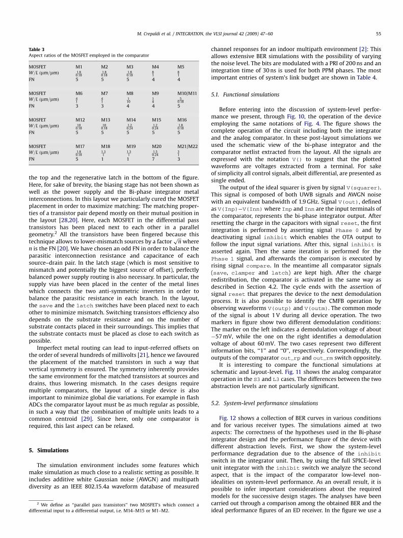
As said before it is of utmost importance that the design non-idealities do not affect the comparator performance. We have thusdetailed the design of this block down to the layout level andanalyzed the parasitic effects on system-level performance thanksto the substitute-and-play methodology previously discussed.Table 3 summarizes the transistors aspect ratios and, consideringthe layout realization, also the finger numbers (FN). Fig. 9 showsthe comparator layout. It is possible to identify the common-mode feedback unit on the right-bottom side, the preamplifier on
ARTICLE IN PRESS
Table 3Aspect ratios of the MOSFET employed in the comparator
MOSFET M1 M2 M3 M4 M5
W=L ðmm=mmÞ 1:80:18
1:80:18
1:80:18
81
81
FN 5 5 5 4 4
MOSFET M6 M7 M8 M9 M10/M11
W=L ðmm=mmÞ 41
41
110
14
50:18
FN 3 3 4 4 5
MOSFET M12 M13 M14 M15 M16
W=L ðmm=mmÞ 100:18
100:18
1:20:24
1:20:24
1:80:18
FN 5 5 5 5 5
MOSFET M17 M18 M19 M20 M21/M22
W=L ðmm=mmÞ 1:80:18
1:31
1:31
1:50:24
31
FN 5 1 1 7 3
M. Crepaldi et al. / INTEGRATION, the VLSI journal 42 (2009) 47–60 55
the top and the regenerative latch in the bottom of the figure.Here, for sake of brevity, the biasing stage has not been shown aswell as the power supply and the Bi-phase integrator metalinterconnections. In this layout we particularly cured the MOSFETplacement in order to maximize matching: The matching proper-ties of a transistor pair depend mostly on their mutual position inthe layout [28,20]. Here, each MOSFET in the differential passtransistors has been placed next to each other in a parallelgeometry.2 All the transistors have been fingered because thistechnique allows to lower-mismatch sources by a factor
ffiffiffinp
wheren is the FN [20]. We have chosen an odd FN in order to balance theparasitic interconnection resistance and capacitance of eachsource–drain pair. In the latch stage (which is most sensitive tomismatch and potentially the biggest source of offset), perfectlybalanced power supply routing is also necessary. In particular, thesupply vias have been placed in the center of the metal lineswhich connects the two anti-symmetric inverters in order tobalance the parasitic resistance in each branch. In the layout,the save and the latch switches have been placed next to eachother to minimize mismatch. Switching transistors efficiency alsodepends on the substrate resistance and on the number ofsubstrate contacts placed in their surroundings. This implies thatthe substrate contacts must be placed as close to each switch aspossible.
Imperfect metal routing can lead to input-referred offsets onthe order of several hundreds of millivolts [21], hence we favouredthe placement of the matched transistors in such a way thatvertical symmetry is ensured. The symmetry inherently providesthe same environment for the matched transistors at sources anddrains, thus lowering mismatch. In the cases designs requiremultiple comparators, the layout of a single device is alsoimportant to minimize global die variations. For example in flashADCs the comparator layout must be as much regular as possible,in such a way that the combination of multiple units leads to acommon centroid [29]. Since here, only one comparator isrequired, this last aspect can be relaxed.
5. Simulations
The simulation environment includes some features whichmake simulation as much close to a realistic setting as possible. Itincludes additive white Gaussian noise (AWGN) and multipathdiversity as an IEEE 802.15.4a waveform database of measured
2 We define as ‘‘parallel pass transistors’’ two MOSFET’s which connect a
differential input to a differential output, i.e. M14–M15 or M1–M2.
channel responses for an indoor multipath environment [2]: Thisallows extensive BER simulations with the possibility of varyingthe noise level. The bits are modulated with a PRI of 200 ns and anintegration time of 30 ns is used for both PPM phases. The mostimportant entries of system’s link budget are shown in Table 4.
5.1. Functional simulations
Before entering into the discussion of system-level perfor-mance we present, through Fig. 10, the operation of the deviceemploying the same notations of Fig. 4. The figure shows thecomplete operation of the circuit including both the integratorand the analog comparator. In these post-layout simulations weused the schematic view of the bi-phase integrator and thecomparator netlist extracted from the layout. All the signals areexpressed with the notation V() to suggest that the plottedwaveforms are voltages extracted from a terminal. For sakeof simplicity all control signals, albeit differential, are presented assingle ended.
The output of the ideal squarer is given by signal V(squarer).This signal is composed of both UWB signals and AWGN noisewith an equivalent bandwidth of 1.9 GHz. Signal V(out), definedas V(Inp)�V(Inn) where Inp and Inn are the input terminals ofthe comparator, represents the bi-phase integrator output. Afterresetting the charge in the capacitors with signal reset, the firstintegration is performed by asserting signal Phase 0 and bydeactivating signal inhibit which enables the OTA output tofollow the input signal variations. After this, signal inhibit isasserted again. Then the same iteration is performed for thePhase 1 signal, and afterwards the comparison is executed byrising signal compare. In the meantime all comparator signals(save, clamper and latch) are kept high. After the chargeredistribution, the comparator is activated in the same way asdescribed in Section 4.2. The cycle ends with the assertion ofsignal reset that prepares the device to the next demodulationprocess. It is also possible to identify the CMFB operation byobserving waveforms V(outp) and V(outm). The common modeof the signal is about 1 V during all device operation. The twomarkers in figure show two different demodulation conditions:The marker on the left indicates a demodulation voltage of about�57 mV, while the one on the right identifies a demodulationvoltage of about 60 mV. The two cases represent two differentinformation bits, ‘‘1’’ and ‘‘0’’, respectively. Correspondingly, theoutputs of the comparator out_rp and out_rm switch oppositely.
It is interesting to compare the functional simulations atschematic and layout-level. Fig. 11 shows the analog comparatoroperation in the S3 and L3 cases. The differences between the twoabstraction levels are not particularly significant.
5.2. System-level performance simulations
Fig. 12 shows a collection of BER curves in various conditionsand for various receiver types. The simulations aimed at twoaspects: The correctness of the hypotheses used in the Bi-phaseintegrator design and the performance figure of the device withdifferent abstraction levels. First, we show the system-levelperformance degradation due to the absence of the inhibit
switch in the integrator unit. Then, by using the full SPICE-levelunit integrator with the inhibit switch we analyze the secondaspect, that is the impact of the comparator low-level non-idealities on system-level performance. As an overall result, it ispossible to infer important considerations about the requiredmodels for the successive design stages. The analyses have beencarried out through a comparison among the obtained BER and theideal performance figures of an ED receiver. In the figure we use a

ARTICLE IN PRESS
Table 4Link budget
Parameter Value
Geometric center frequency (f 0c) 3.94 GHz
Average TX power (PT) �8.5 dBm
RX noise figure (NF) 7 dB
Minimum Eb=N0 for BER ¼ 10�3 (S) 17 dB
Implementation loss (I) 1 dB
Link margin ðat dmax ¼ 26 mÞ 1.22 dB
Minimum RX sensitivity level �87 dBm
Fig. 9. Comparator layout.
M. Crepaldi et al. / INTEGRATION, the VLSI journal 42 (2009) 47–6056
symbolic notation to denote the modeling levels for the receiverblocks. The front-end, the comparator and the Bi-phase integratorare represented by symbols F, C and B, while the values in bracketsfor these symbols, as defined in Section 3, represent the abstractionlevel: P1—Conceptual Phase I, P2—Behavioral Phase II, P3-S—
SPICE-level Phase III, P3-L—Post-layout level Phase III.The ‘‘Analytic’’ curve refers to a theoretical ED receiver with
infinite quantization resolution [30]. The F(P1) curve refers to aquantization resolution of 5 bits. The other cases refer to thereduced complexity receiver described by a B(P3-S) Bi-phaseintegrator for different abstraction levels of the comparator. In allthese cases, the demodulator input range is 160 mV. In case noreset switches across Cp are considered, performance degrades
significantly. As previously shown in (5), demodulation is affectedby the voltage across Cp stored in each operation phase and bythe output voltage of the previous demodulation cycle. If in theintegrator no inhibit signal is used, the terms Np;ðnÞ
fph0for the first
integration phase and the corresponding Np;ðnÞfph1
for the second onecorrupt the final demodulation voltage: Thus, demodulationperformance decreases even with an ideal P2 comparator. In fact,figure shows that the equivalent quantization resolution is worsethan an ideal receiver with a 5 bit resolution A/D. On the otherhand, thanks to the Inhibit switches, the bi-phase integrator canapproximately reach the performance of the theoretical EDreceiver (BER curves overlap). The offset rejection feature of thedevice is also proven because BER remains almost unvaried if aninput-referred offset VOS of 40 mV is included in the simulations.These important results permit to verify the correctness of thepreviously presented theory.
For completeness, Fig. 12 includes other impulse-radio receivertypes, transmitted reference (TR) and on–off keying (OOK) [31].The curves show better BER performance of ED compared to TR inwhich no threshold set is required for demodulation. In the case ofOOK receivers setting a threshold is mandatory and affectsperformance. In this case it has slightly worse performance thanED even though the optimal threshold was chosen.
It is possible to note that the curves B(P3-S)–C(P3-L) andB(P3-S)–C(P3-S) comparator models differ slightly especially

ARTICLE IN PRESS
Fig. 10. Transient simulation of the bi-phase demodulator.
M. Crepaldi et al. / INTEGRATION, the VLSI journal 42 (2009) 47–60 57
for low-SNR. Since the bi-phase integrator output voltage is lowand comparable to the input-referred offset of the comparatorstage, for low Eb=N0 the non-perfect routing in the comparatorinterconnections generate an input-referred offset which slightlyincreases the error-rate. For higher Eb=N0 this unbalanced routingdo not influence system-level performance because the finaldemodulation voltage after charge redistribution is higher.
Fig. 13 shows the BER of the demodulator at Eb=N0 ¼17 dB—which corresponds to an acceptably low-BER—as afunction of the OTA input signal amplitude. For input signalslower than input range of the OTA (on the order of 250 mV), theBER does not change. Whether the input signal becomes larger,the BER performance decreases. As anticipated in Section 4, thisdistortion does not degrade much the BER figure because OTAsaturates only for very short times, corresponding to the durationof the peaks of the UWB signal exceeding the input range. Thisleads only to a slight degradation of the BER. For example anincrease of input amplitude from 250 to 450 mV leads to a BERdegradation of 10�4. As input signal further increases, this effectbecomes more relevant, especially at very low-signal-to-noiseratios.
The most important non-ideal effect which degrades demo-dulator performance is related to the input-referred offset of thecomparator due to transistor mismatch. Especially at low-SNR,since noise power level is comparable to UWB signal strength, theoutput voltage of the integrator is comparable to the input-referred offset of the comparator. The simulation with input offsetvoltage up to 10 mV do not show BER degradation if the inputsignal level is sufficiently high. This requires having an overallgain of the front-end before the OTA of 40 dB, which is compatiblewith other works [7].
The curves of Figs. 12 and 13 identify the limits below whichthe receiver works almost ideally. If input signal’s amplitude isbelow 250 mV and input-referred offset is less than 40 mV, theresults are more or less the same regardless of the abstraction
level used for the various blocks, that is AMS, schematic or layoutlevel. Therefore, in order to save simulation time, it is possible todesign the remaining part and simulate the whole receiver’s frontend by using a P2 view of the already designed blocks. A summaryof the obtained results both at circuit and system level is shown inTable 5. As far as performance in concerned, there is no BERdegradation with respect to the ideal case using a P1 or P2description, as physical effects are abstracted away. On thecontrary, schematic and layout level P3 descriptions allow toinclude and evaluate such effects.
Table 5 also summarized power consumption figures that canbe evaluated in P3. When the device is idle and no signal ispresent at the input, the quiescent power consumption PQ ,inclusive of biasing circuit, is 400mW. During normal operation,the power consumption PD, averaged on 4 ms of demodulationactivity, is 1 mW in P3-S and 950mW in P3-L because theoptimized layout has smaller parasitics than the overestimatedones of the schematic level. With respect to [7], in which theoverall receiver consumes 2.5 nJ/bit at 16.7 Mbit/s Val ¼ 0:65 V,here the energy spent by the demodulator is 190 pJ/bit at 5 Mbit/sand Eb=N0 ¼ 15 dB, Val ¼ 1:8 V.
Typical UWB receiver implementations have power consump-tion ranging from 1 to 330 mW. This huge diversity is due to thetransmission technology used, multi-band-OFDM or impulse-radio and to the technology process. For the impulse-radio PPMreceivers power consumption is in the range 30–40 mW andenergy per bit varies between 1 and 3 nJ/bit. The highest powercontribution is due to the front-end units, which must provide again of about 40 dB [7]. Supposing the power gain of a single LNAcannot exceed 20 dB in the best case, the required front-end gaincan be obtained by cascading one LNA with other gain stages.Typically the LNAs for impulse-radio would consume 9 mW [32].Since our demodulator consumes only 1 mW and its area is waysmaller than the first RF front-end units, it contributes onlyfor a small portion of the power-area budget. Wrapping up the

ARTICLE IN PRESS
5 7 9 11 13 15 17
10−3
10−2
10−1
100
Eb/N0 (dB)
BE
R
B(P3−S), C(P3−S), No Inhibit, VOS = 0V
B(P3−S), C(P3−S), Inhibit, VOS = 0V
B(P3−S), C(P3−S), Inhibit, VOS = 40mV
B(P3−S), C(P3−L), Inhibit, VOS = 0V
F(P1), Energy Detection curve (5 bit res.)
Non−coherent OOK receiver
Non−coherent TR receiver
Energy Detection (∞ res.) − Analytic
Fig. 12. BER curves comparison at different abstraction levels.
Fig. 11. Comparison between the circuit and post-layout level of the comparator unit.
M. Crepaldi et al. / INTEGRATION, the VLSI journal 42 (2009) 47–6058

ARTICLE IN PRESS
200 250 300 350 400 450 500 550 600 650
0.00050.00060.00070.00080.0009
0.001
0.002
OTA Input amplitude (mVpp)
BE
R
Fig. 13. BER at Eb=N0 ¼ 17 dB for various input amplitudes.
Table 5Results obtained during the refinement phases P1, P2 and P3
P1 P2
Circuit-level None Block identification
System-level (BER) Ideal ED receiver Ideal ED receiver
P3-S P3-L (hybrid P3-S/P3-L)
Circuit-level PQ ¼ 400mW, PD ¼ 1 mW PQ ¼ 400mW,
PD ¼ 950mW
System-level (BER) Fig. 12, B(P3-S)-C(P3-S),
almost idealFig. 13, 10�4 loss at
450 mV swing
M. Crepaldi et al. / INTEGRATION, the VLSI journal 42 (2009) 47–60 59
obtained results with other data from the literature we can expecta peak power of 15–20 mW for the overall receiver. Moreover, it isunderstood that wireless applications in which IR-UWB is boundto be employed will work at extremely low-duty-cycles, thusallowing to switch off the front-end blocks during idle timestherefore reducing power to a few percent of the peak [33].
Another important consideration regarding the performance ofED UWB receivers is narrow-band interference. The BER perfor-mance depends on the strength, number and physical position ofthe transmitters [34]. Provided that the receiver front-end doesnot saturate, since the demodulator has about ideal performance,the effect of interference is about the same as for ideal EDreceivers. Hence, for decreasing interference sensitivity weaddress the reader to the specific literature. For instance, in TRreceivers attenuating in-band interference by using notch filtersor increasing signal-to-interference ratios (SIR) by using feedbackloop mechanisms are standard techniques [35].
It is also fundamental that receiver can recover synchroniza-tion in presence of such a simplified hardware. We demonstratedin [36] how to achieve synchronization with this simple Bi-phasedemodulator. The synchronization functionality is obtained usingonly the 1-bit output of the comparator and a searchbackalgorithm applied on an ordered collection of differentialenergies: These are obtained by delaying the Phase 0 andPhase 1 windows and by shifting the integrations linearly withinthe PRI.
6. Conclusions
This paper presented a new CMOS 0:18mm 2-PPM demodu-lator architecture based on a Gm � C open loop integrator, aswitched capacitor network and an analog comparator. The circuithas been designed and simulated using an ad hoc methodologybased on a ‘‘substitute-and-play’’ approach which allows tochange the abstraction level in the simulations. Thanks to an adhoc testbed and the simulation tool ADVanceMS, it is possible to
change the block descriptions and modify the simulationaccuracy. The environment employs a realistic channel modeland offers the possibility to include both BSIM3 MOSFET andlayout backannotated models with distributed RC parasitics. BERresults show that the device has about the same performance ofan ideal ED receiver employing infinite A/D resolution.
Once the circuit layout has been fully completed, mixed-signalinsulation techniques will be essential to prevent that the otherfront-end devices compromise the transconductor and thecomparator operations. Considering the results obtained in thiswork, final design steps such as layout of the bi-phase integratorand silicon fabrication are worthy of consideration, and we plan tofocus on that our forthcoming work.
References
[1] Revision of part 15 of the commissions rules regarding ultra-widebandtransmission systems, Report and Order, adopted February 14, 2002, releasedJuly 15, 2002, FCC.
[2] IEEE 802.15 WPAN low rate alternative PHY task group 4A (TG4A) [Online].Available: hhttp://www.ieee802.org/15/pub/TG4a.htmli.
[3] F.S.L. David, D. Wentzloffe, et al., Energy efficient pulsed-UWB CMOS circuitsand systems, in: Proceedings of the International Conference on UWB 2007,September 2007, pp. 282–287.
[4] L. Stoica, et al., An ultrawideband system architecture for tag-based wirelesssensor networks, IEEE Trans. Veh. Technol. 54 (5) (2005) 1632–1645.
[5] R.B. Fred S. Lee, et al., A 3.1 to 10.6 GHz 100 Mb/s pulse-based ultra-widebandradio receiver chipset, in: Proceedings of the International Conference onUWB 2006, January 2006, pp. 185–190.
[6] F.S. Lee, A.P. Chandrakasan, A 2.5 nJ/b 0.65 V 3-to-5 GHz subbanded UWBreceiver in 90 nm CMOS, in: Proceedings of the IEEE ISSCC, 2007, pp. 116–590.
[7] F.S. Lee, A.P. Chandrakasan, A 2.5 nJ/bit 0.65 V pulsed UWB receiver in 90 nmCMOS, IEEE J. Solid-State Circuits 42 (12) (2007) 2851–2859.
[8] E. Christen, K. Bakalar, VHDL-AMS—a hardware description language foranalog and mixed-signal applications, IEEE Trans. Circuits Syst. II 46 (10)(1999) 1263–1272.
[9] L. Barrandon, et al., Behavioral modeling and simulation of mixed signalfront-end for software defined radio terminals, in: Proceedings of the IEEEInternational Symposium on Industrial Electronics 2004, May 2004.
[10] V. Nguyen, et al., VHDL-AMS behavioral modelling and simulation of high-pass delta-sigma modulator, in: Proceedings of the IEEE InternationalBehavioral Modeling and Simulation Conference (BMAS’05), San Jose, CA,October 2005, pp. 106–111.
[11] M. Crepaldi, et al., An effective AMS top-down methodology applied to thedesign of a mixed-signal uwb system-on-chip, in: Proceedings of the DATE2007, Nice, France, April 2007.
[12] M. Crepaldi, et al., UWB receiver design and two-way-ranging simulationusing VHDL-AMS, in: Proceedings of the PRIME 2006, Otranto, Italy, June2006.
[13] E. Sanchez-Sinencio, et al., CMOS transconductance amplifiers, architecturesand active filters: a tutorial, in: IEE Proceedings—Circuits Devices Systems,February 2000.
[14] B. Razavi, Design of Analog CMOS Integrated Circuits, International Edition,McGraw-Hill, New York, 2001.
[15] J. Moreira, et al., Limits to the dynamic range of low-power continuous-timeintegrators, IEEE Trans. Circuits Syst. I 48 (7) (2001) 805–817.
[16] J. Galan, et al., A low-power low-voltage OTA-C sinusoidal oscillator with alarge tuning range, IEEE Trans. Circuits Syst. I 52 (2) (2005) 283–291.
[17] S.-H. Yang, et al., A novel CMOS operational transconductance amplifier basedon a mobility compensation technique, IEEE Trans. Circuits Syst. II 52 (1)(2005) 37–42.
[18] P.M. Figueiredo, J.C. Vital, Kickback noise reduction techniques for CMOSlatched comparators, IEEE Trans. Circuits Syst. I 53 (7) (2006) 541–545.
[19] S. Park, M.P. Flynn, A regenerative comparator structure with integratedinductors, IEEE Trans. Circuits Syst. I 53 (8) (2006) 1704–1711.
[20] P.G. Drennan, C.C. McAndrew, Understanding MOSFET mismatch for analogdesign, IEEE J. Solid-State Circuits 38 (3) (2003) 450–456.
[21] A. Nikoozadeh, B. Murmann, An analysis of latch comparator offset due toload capacitor mismatch, IEEE Trans. Circuits Syst. II 53 (12) (2006)1398–1402.
[22] K. Kotani, et al., CMOS charge-transfer preamplifier for offset-fluctuationcancellation in low-power A/D converters, IEEE J. Solid-State Circuits 33 (5)(1998) 762–769.
[23] B. Razavi, B.A. Wooley, Design techniques for high-speed, high-resolutioncomparators, IEEE J. Solid-State Circuits 27 (12) (1992) 1916–1926.
[24] B.P. Ginsburg, A.P. Chandrakasan, Dual time-interleaved successive approx-imation register ADCs for an ultra-wideband receiver, IEEE J. Solid-StateCircuits 42 (2) (2007) 247–257.
[25] J.H. Atherton, H.T. Simmonds, An offset reduction technique for use withCMOS integrated comparators and amplifiers, IEEE J. Solid-State Circuits 27(8) (1992) 1168–1175.

ARTICLE IN PRESS
M. Crepaldi et al. / INTEGRATION, the VLSI journal 42 (2009) 47–6060
[26] M.-J.E. Lee, et al., Low-power area-efficient high-speed i/o circuit techniques,IEEE J. Solid-State Circuits 35 (11) (2000) 1591–1599.
[27] S.R.S.N. Stefanou, An average low offset comparator for 1.25 Gsample/s ADC in0.18micron CMOS, in: Proceedings of the IEEE International Conference onElectronics Circuits and Systems, December 2004, pp. 246–249.
[28] M.J. Pelgrom, et al., Matching properties of MOS transistors, IEEE J. Solid-StateCircuits 24 (5) (1989) 1433–1440.
[29] S. Bhattacharya, et al., Multi-level symmetry constraint generation forretargeting large analog layouts, IEEE Trans. Comput. Aided Des. 25 (6)(2006) 945–960.
[30] C. Carbonelli, U. Mengali, M-PPM noncoherent receivers for UWB applica-tions, IEEE Trans. Wireless Commun. 5 (8) (2006) 2285–2294.
[31] S. Dubouloz, et al., Performance analysis of LDR UWB non-coherent receiversin multipath environments, in: Proceedings of the IEEE InternationalConference on UWB, September 2005, pp. 491–496.
[32] A. Bevilacqua, A.M. Niknejad, An ultra-wideband CMOS LNA for 3.1 to10.6 GHz wireless receiver, in: Proceedings of the IEEE ISSCC Digest ofTechnical Papers, 2004, pp. 382–383.
[33] R.W.B. Ian, D. O’Donnell, A flexible, low power, DC-1 GHz impulse-UWBtransceiver front-end, in: Proceedings of the International Conference onUWB 2006, January 2006, pp. 275–280.
[34] A. Rabbachin, et al., UWB energy detection in the presence of multiplenarrowband interferers, in: Proceedings of the IEEE International Conferenceon UWB, September 2007, pp. 857–862.
[35] F. Dowla, et al., Interference mitigation in transmitted-reference ultra-wideband (UWB) receivers, in: Proceedings of the IEEE Antennas andPropagation Society International Symposium, June 2004, pp. 1307–1310.
[36] M. Crepaldi, et al., A 1-bit synchronization algorithm for a reduced complex-ity energy detection UWB receiver, in: International Conference on UWB,September 2007.
Marco Crepaldi received the D.Eng. degree in electro-nics engineering (summa cum laude) from the Politec-nico di Torino, Turin, Italy, in 2005, where he iscurrently pursuing the Ph.D. degree. He is currently aVisiting Scholar at Columbia University in the City ofNew York. His research interests are VHDL-AMSbehavioral modeling of analog and mixed-signalcircuits and ultra-wide-band communications at sys-tem and circuit level.
Mario R. Casu (M’05) received the electronics engineerdegree (summa cum laude) and the Ph.D. degree fromthe Politecnico di Torino, Turin, Italy, in 1998 and 2002,respectively. He is an Assistant Professor in Depart-ment of Electronics, Politecnico di Torino. His interestsencompass CAD aspects of deep-submicrometer CMOStechnologies, architectural and register transfer leveldesign of multiprocessors systems-on-chip and mixed-signal design for ultra-wide-band applications.
Mariagrazia Graziano (M’07) received the D.Eng.degree in electronics engineering and the Ph.D. degreein electronic and communication engineering from thePolitecnico di Torino, Turin, Italy, in 1997 and 2001,respectively. From 1999 to 2000 she was a VisitingScholar at University of Illinois at Chicago. Since 2002she has been an Assistant Professor at the Politecnicodi Torino. Her research interests include the design ofultra-wide-band CMOS transceivers and the develop-ment of models and algorithms for the design of CMOSnoise-tolerant digital and mixed-signal circuits.
Maurizio Zamboni received the electronics engineerdegree and the Ph.D. degree, from the Politecnico deTorino, Torino, Italy, in 1983 and 1988, respectively. In1983, he joined the Electronics Department, Politecni-co di Torino, where he became a researcher in 1989,and an associate professor in 1992. Since 1992, he hasbeen teaching a course in applied electronics and since1993, he has been teaching a course in integratedcircuits architectures. His research activity began withthe study of multiprocessor architectures, followed bywork with digital IC design. His current researchinterests include the design of special ICs for artificial
intelligence, vision and telecommunication. He hasworked with several European projects in the field of ATM networks and digitaltelevision. He is coauthor of more than 60 scientific papers and has two patents.