a level-crossing flash asynchronous analog-to · pdf filea level-crossing flash asynchronous...
TRANSCRIPT
A Level-Crossing Flash Asynchronous Analog-to-Digital Converter
Filipp Akopyan, Rajit Manohar, Alyssa B. Apsel∗
Computer Systems LaboratoryElectrical and Computer Engineering
Cornell UniversityIthaca, NY 14853, U.S.A.
Abstract
Distributed sensor networks, human body implants, andhand-held electronics have tight energy budgets that ne-cessitate low power circuits. Most of these devices in-clude an analog-to-digital converter (ADC) to process ana-log signals from the physical world. We describe a newtopology for an asynchronous analog-to-digital converter,dubbed LCF-ADC, that has several major advantages overpreviously-designed ADCs, including reduced energy con-sumption and/or a simplification of the analog circuits re-quired for its implementation.
In this paper we describe the design of the LCF-ADCarchitecture, and present simulation results that show lowpower consumption. We discuss both theoretical considera-tions that determine the performance of our ADC as wellas a proposed implementation. Comparisons with previ-ously designed asynchronous analog-to-digital convertersshow the benefits of the LCF-ADC architecture. In 180 nmCMOS, our ADC is expected to consume 43 µW at 160 kHz,and 438 µW at 5 MHz.
1 Introduction
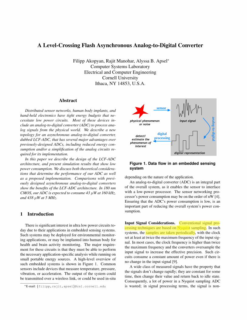
There is significant interest in ultra low power circuits to-day due to their applications in embedded sensing systems.Such systems may be deployed for environmental monitor-ing applications, or may be implanted into human body forhealth and brain activity monitoring. The major require-ment for these circuits is that they must be able to performthe necessary application-specific analysis while running onsmall portable energy sources. A high-level overview ofsuch embedded systems is shown in Figure 1. Commonsensors include devices that measure temperature, pressure,vibration, or acceleration. The output of the system couldbe transmitted over a wireless link, or could be used in-situ
∗E-mail: filipp,rajit,[email protected]
input signalphysical phenomenonor noise
digital representation
detect/estimate the
phenomenon of interest
sensor
analog-to-digital
digitalprocessing
Figure 1. Data flow in an embedded sensingsystem
depending on the nature of the application.An analog-to-digital converter (ADC) is an integral part
of the overall system, as it enables the sensor to interfacewith a low-power processor. The sensor networking pro-cessor’s power consumption may be on the order of nW [4].Ensuring that the ADC’s power consumption is low, is animportant part of reducing the overall system’s power con-sumption.
Input Signal Considerations. Conventional signal pro-cessing techniques are based on Nyquist sampling. In suchsystems, the samples are taken periodically, with the clockset at least at twice the maximum frequency of the input sig-nal. In most cases, the clock frequency is higher than twicethe maximum frequency and the converters oversample theinput signal to increase the effective precision. Such cir-cuits consume a constant amount of power even if there isno change in the input signal [9].
A wide class of measured signals have the property thatthe signals don’t change rapidly; they are constant for sometime, then change their value and return back to idle state.Consequently, a lot of power in a Nyquist sampling ADCis wasted; in signal processing terms, the signal is non-
stationary and therefore the optimal sampling rate shouldadapt based on the signal characteristics. For the purpose ofeliminating the circuit power consumption when the input isstable, we use two existing techniques to design the ADC:(i) we adopt an asynchronous event-driven circuit approach,these circuits idle when there is no change at the input;(ii) we adopt an implicit sampling approach, also knownas level-crossing sampling.
Sampling scheme. The level-crossing scheme is non-uniform in time domain; it is based on the concept of pre-determined reference levels, where a sample is taken onlyif a reference level is crossed. The samples are not takenat a constant rate, but are only obtained if there is a suffi-cient change in the input analog signal. A simple version ofthis approach that only detects the sign of the input signal(zero-crossing sampling) has been extensively studied bythe signal processing community beginning with the workof Rice [23]. Kedem provides an excellent overview of thework in this area [10]. The concept of level-crossing sam-pling has been previously studied as a method of samplingutilized in analog-to-digital conversion and in data com-pression [18, 25]. More recently, Renaudin et al. developedan ADC using the level-crossing approach [2].
Contributions. We present a new topology for an asyn-chronous level-crossing-based ADC (LCF-ADC). UnlikeRenaudin’s approach, the time in the LCF-ADC is nottracked explicitly. Each level-crossing event is representedby a one-bit data token produced at the output. The value“1” indicates that the input signal has crossed the givenlevel from below; the value “0” indicates that the inputsignal has crossed the level from above. Using the ob-tained bit sequence (differential encoding: only 1-s and0-s), downstream processing of the binary stream can beimplemented [11]. This type of encoding is known asasynchronous delta modulation; it was proposed by Watan-abe [8] and was previously used by Tsividis [14, 15]. Inaddition, the LCF-ADC can be configured in such a waythat it detects the situation when the input signal exceeds itsdesign parameters, and this detection can be used to activatea more sophisticated ADC if necessary. As stated in the ab-stract, in 180 nm CMOS, our ADC is expected to consume43 µW at 160 kHz, and 438 µW at 5 MHz.
Related Work. There is an enormous body of literatureon ADCs, including several books on the subject [9]. Acomparison of using synchronous and asynchronous meth-ods [13] for ADCs studied the effect of using asynchronouslogic in ADC implementations; previously, a flash-typeADC was implemented using micropipelines [12].
Recently, several schemes utilizing level-crossing weredeveloped [1, 2]. However, the goal of those designs is sig-
nal reconstruction. Those systems record sample time andreconstruct the original signal to perform signal processingoperations. Instead, our idea is to process the level cross-ings without reconstructing the original input. As shown byKedem [11], such processing is possible by directly formu-lating detection and estimation problems with the implicitsignal representation. Tsividis has demonstrated advantagesof continuous time signal processing utilizing only a quan-tizer [27].
In our architecture we do not record the times at whichthe samples are taken. This technique reduces the powerconsumption even further by eliminating the circuitry thatdeals with time-tracking. In case we need to reconstructthe original signal, the time information is still embeddedin the relative delays of the output samples. This infor-mation can be extracted at any time if necessary, by themeans of a simple digital counter (and calculating the timeelapsed since the previous sample has appeared at the out-put), which can be easily added to our circuit. Our approachadopts a completely different ADC topology: instead ofusing the feedback-based approach adopted by Renaudin(and, following Renaudin, by Shepard [14]), we use a par-allel architecture that resembles a flash-type ADC.
2 LCF-ADC Architecture
The LCF-ADC architecture is a mixed-signal circuit,containing analog parts and asynchronous digital parts.For the design of the asynchronous digital circuits weuse the quasi-delay-insensitive (QDI) style [20] due toits robustness to process, voltage, and temperature varia-tions. The circuits are implemented using Martin’s synthe-sis method [19] that translates a high-level design descrip-tion to circuits through handshaking expansions, and pro-duction rules.
When designing the LCF-ADC, our main goal was tominimize the ADC’s power consumption, while still main-taining a reasonable frequency of operation. Our LCF-ADCwas optimized for the input signal bandwidth of 5 MHz.We chose this requirement based upon a survey that exam-ines bandwidths of commercially available sensors includ-ing pressure sensors, temperature sensors, and accelerome-ters.
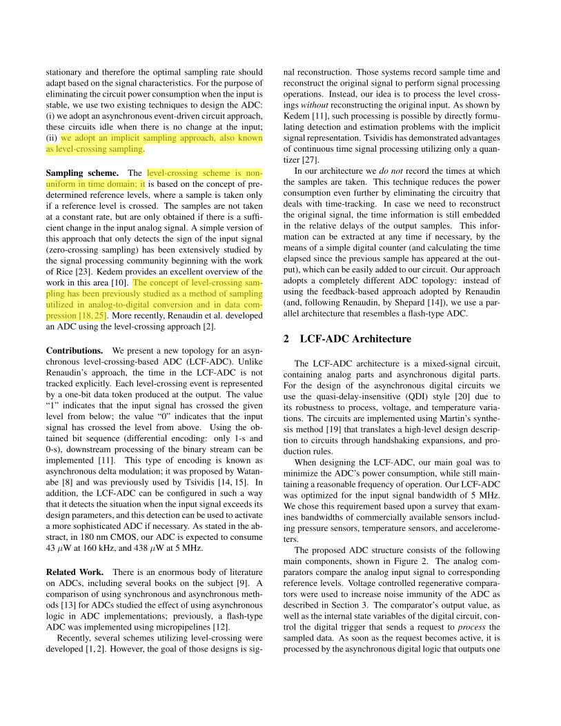
The proposed ADC structure consists of the followingmain components, shown in Figure 2. The analog com-parators compare the analog input signal to correspondingreference levels. Voltage controlled regenerative compara-tors were used to increase noise immunity of the ADC asdescribed in Section 3. The comparator’s output value, aswell as the internal state variables of the digital circuit, con-trol the digital trigger that sends a request to process thesampled data. As soon as the request becomes active, it isprocessed by the asynchronous digital logic that outputs one
AsynchronousCircuitry
MERGE
Element
Comparators
AsynchronousProcessing
token
CircuitryAnalog
Vref2
Vref2m
Vref1
Vin
Figure 2. Proposed ADC Structure
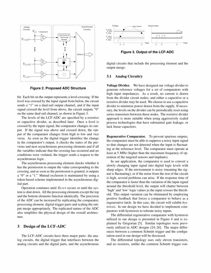
bit. Each bit on the output represents a level-crossing. If thelevel was crossed by the input signal from below, the circuitsends a “1” on a dual-rail output channel, and if the inputsignal crossed the level from above, the circuit outputs “0”on the same dual rail channel, as shown in Figure 3.
The levels of the LCF-ADC are specified by a resistiveor capacitive divider, as described later. Once a level iscrossed by the input signal, the comparator changes its out-put. If the signal was above and crossed down, the out-put of the comparator changes from high to low and viceversa. As soon as the digital trigger identifies the changein the comparator’s output, it checks the states of the pre-vious and next asynchronous processing elements and if allthe variables indicate that the crossing has occurred and noconditions were violated, the trigger sends a request to theasynchronous logic.
The asynchronous processing element checks whether ithas the permission to output the value corresponding to thecrossing, and as soon as the permission is granted, it outputsa “0” or a “1.” Mutual exclusion is maintained by using atoken-based scheme implemented in the asynchronous dig-ital part.
Operation continues until Reset occurs or until the sys-tem is shut down. All the processing elements except the topand the bottom elements function identically. The precisionof the ADC can be increased by replicating the comparator,processing element, digital trigger parts and scaling the out-put merge appropriately. The replicated nature of the ADCalso simplifies the physical design of the overall architec-ture.
3 Design of the LCF-ADC
The LCF-ADC circuits have three major parts: the ana-log circuits, the digital trigger that interfaces between theanalog circuits and the digital parts, and the asynchronous
t3
Voltage
V_ref2
V_trig+V_ref1
V_trig−
V_trig−
V_trig+
Time Time
"1"
"0"
Digital OutputInput Signal
t1 t2 t3t1 t2
Figure 3. Output of the LCF-ADC
digital circuits that include the processing element and theoutput merge.
3.1 Analog Circuitry
Voltage Divider. We have designed our voltage divider togenerate reference voltages for a set of comparators withhigh input impedances. As a result, no current is drawnfrom the divider circuit nodes; and either a capacitive or aresistive divider may be used. We choose to use a capacitivedivider to minimize power drawn from the supply. If neces-sary, the levels on the divider can be periodically reset usingseries transistors between those nodes. The resistive dividerapproach is more suitable when using aggressively scaledprocess technologies that have substantial gate leakage, orlack linear capacitors.
Regenerative Comparator. To prevent spurious outputs,the comparator must be able to suppress a noisy input signalso that changes are not detected when the input is fluctuat-ing at the reference level. The comparator must operate atleast at 5 MHz (higher than the maximum frequency of op-eration of the targeted sensors and implants).
In our application, the comparator is used to convert aslowly changing input signal into digital logic levels withsharp edges. If the environment is noisy (meaning the sig-nal is fluctuating), or if the noise from the rest of the circuitis high, several problems can arise. If the response time ofthe comparator is faster than the variation of the input signalaround the threshold level, the output will chatter between’high’ and ’low’ logic values as the input crosses the thresh-old. This output variation can be eliminated by employingpositive feedback that forces a comparator to behave as aregenerative latch. In this case, the circuit will exhibit hys-teresis. In our design we have decided to implement com-parators with hysteresis to tolerate noisy inputs.
The differential regenerative comparator with hysteresisutilized in our design is presented in Figure 4 and is ex-plained by Gregorian [5]. Similar topologies were previ-ously utilized in ADC designs [24, 26]. The major differ-ences between a common Schmitt trigger and the configu-ration used in our design will be discussed.
The differential topology uses only eleven transistors,and no resistors, unlike the common Schmitt trigger con-
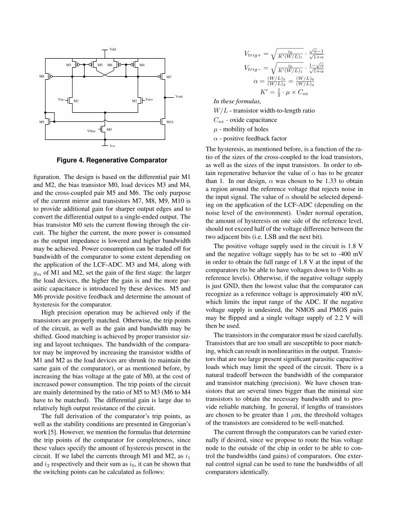
M9
Vdd
VoutVin− Vin+
Vbias
Vss
M3 M5 M6 M4
M7M8
M1 M2
M10
M0
Figure 4. Regenerative Comparator
figuration. The design is based on the differential pair M1and M2, the bias transistor M0, load devices M3 and M4,and the cross-coupled pair M5 and M6. The only purposeof the current mirror and transistors M7, M8, M9, M10 isto provide additional gain for sharper output edges and toconvert the differential output to a single-ended output. Thebias transistor M0 sets the current flowing through the cir-cuit. The higher the current, the more power is consumedas the output impedance is lowered and higher bandwidthmay be achieved. Power consumption can be traded off forbandwidth of the comparator to some extent depending onthe application of the LCF-ADC. M3 and M4, along withgm of M1 and M2, set the gain of the first stage: the largerthe load devices, the higher the gain is and the more par-asitic capacitance is introduced by these devices. M5 andM6 provide positive feedback and determine the amount ofhysteresis for the comparator.
High precision operation may be achieved only if thetransistors are properly matched. Otherwise, the trip pointsof the circuit, as well as the gain and bandwidth may beshifted. Good matching is achieved by proper transistor siz-ing and layout techniques. The bandwidth of the compara-tor may be improved by increasing the transistor widths ofM1 and M2 as the load devices are shrunk (to maintain thesame gain of the comparator), or as mentioned before, byincreasing the bias voltage at the gate of M0, at the cost ofincreased power consumption. The trip points of the circuitare mainly determined by the ratio of M5 to M3 (M6 to M4have to be matched). The differential gain is large due torelatively high output resistance of the circuit.
The full derivation of the comparator’s trip points, aswell as the stability conditions are presented in Gregorian’swork [5]. However, we mention the formulas that determinethe trip points of the comparator for completeness, sincethese values specify the amount of hysteresis present in thecircuit. If we label the currents through M1 and M2, as i1and i2 respectively and their sum as i0, it can be shown thatthe switching points can be calculated as follows:
Vtrig+ =√
i0K′(W/L)1
·√
α−1√1+α
Vtrig− =√
i0K′(W/L)1
· 1−√
α√1+α
α = (W/L)5(W/L)3
= (W/L)6(W/L)4
K ′ = 12 · µ× Cox
In these formulas,W/L - transistor width-to-length ratioCox - oxide capacitanceµ - mobility of holesα - positive feedback factor
The hysteresis, as mentioned before, is a function of the ra-tio of the sizes of the cross-coupled to the load transistors,as well as the sizes of the input transistors. In order to ob-tain regenerative behavior the value of α has to be greaterthan 1. In our design, α was chosen to be 1.33 to obtaina region around the reference voltage that rejects noise inthe input signal. The value of α should be selected depend-ing on the application of the LCF-ADC (depending on thenoise level of the environment). Under normal operation,the amount of hysteresis on one side of the reference level,should not exceed half of the voltage difference between thetwo adjacent bits (i.e. LSB and the next bit).
The positive voltage supply used in the circuit is 1.8 Vand the negative voltage supply has to be set to -400 mVin order to obtain the full range of 1.8 V at the input of thecomparators (to be able to have voltages down to 0 Volts asreference levels). Otherwise, if the negative voltage supplyis just GND, then the lowest value that the comparator canrecognize as a reference voltage is approximately 400 mV,which limits the input range of the ADC. If the negativevoltage supply is undesired, the NMOS and PMOS pairsmay be flipped and a single voltage supply of 2.2 V willthen be used.
The transistors in the comparator must be sized carefully.Transistors that are too small are susceptible to poor match-ing, which can result in nonlinearities in the output. Transis-tors that are too large present significant parasitic capacitiveloads which may limit the speed of the circuit. There is anatural tradeoff between the bandwidth of the comparatorand transistor matching (precision). We have chosen tran-sistors that are several times bigger than the minimal sizetransistors to obtain the necessary bandwidth and to pro-vide reliable matching. In general, if lengths of transistorsare chosen to be greater than 1 µm, the threshold voltagesof the transistors are considered to be well-matched.
The current through the comparators can be varied exter-nally if desired, since we propose to route the bias voltagenode to the outside of the chip in order to be able to con-trol the bandwidths (and gains) of comparators. One exter-nal control signal can be used to tune the bandwidths of allcomparators identically.
3.2 Digital Circuitry
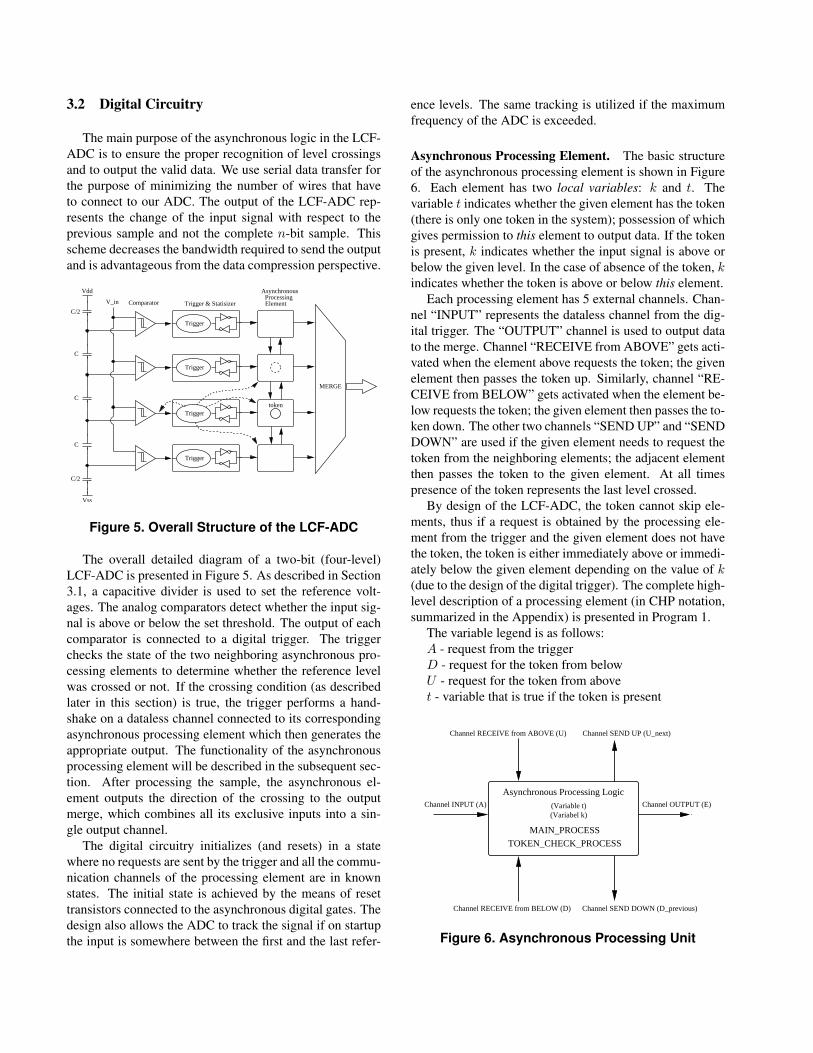
The main purpose of the asynchronous logic in the LCF-ADC is to ensure the proper recognition of level crossingsand to output the valid data. We use serial data transfer forthe purpose of minimizing the number of wires that haveto connect to our ADC. The output of the LCF-ADC rep-resents the change of the input signal with respect to theprevious sample and not the complete n-bit sample. Thisscheme decreases the bandwidth required to send the outputand is advantageous from the data compression perspective.
MERGE
Trigger & StatisizerComparator
Vdd
C/2
C
C
C
C/2
V_in
Trigger
Trigger
Trigger
Trigger
AsynchronousProcessingElement
Vss
token
Figure 5. Overall Structure of the LCF-ADC
The overall detailed diagram of a two-bit (four-level)LCF-ADC is presented in Figure 5. As described in Section3.1, a capacitive divider is used to set the reference volt-ages. The analog comparators detect whether the input sig-nal is above or below the set threshold. The output of eachcomparator is connected to a digital trigger. The triggerchecks the state of the two neighboring asynchronous pro-cessing elements to determine whether the reference levelwas crossed or not. If the crossing condition (as describedlater in this section) is true, the trigger performs a hand-shake on a dataless channel connected to its correspondingasynchronous processing element which then generates theappropriate output. The functionality of the asynchronousprocessing element will be described in the subsequent sec-tion. After processing the sample, the asynchronous el-ement outputs the direction of the crossing to the outputmerge, which combines all its exclusive inputs into a sin-gle output channel.
The digital circuitry initializes (and resets) in a statewhere no requests are sent by the trigger and all the commu-nication channels of the processing element are in knownstates. The initial state is achieved by the means of resettransistors connected to the asynchronous digital gates. Thedesign also allows the ADC to track the signal if on startupthe input is somewhere between the first and the last refer-
ence levels. The same tracking is utilized if the maximumfrequency of the ADC is exceeded.
Asynchronous Processing Element. The basic structureof the asynchronous processing element is shown in Figure6. Each element has two local variables: k and t. Thevariable t indicates whether the given element has the token(there is only one token in the system); possession of whichgives permission to this element to output data. If the tokenis present, k indicates whether the input signal is above orbelow the given level. In the case of absence of the token, kindicates whether the token is above or below this element.
Each processing element has 5 external channels. Chan-nel “INPUT” represents the dataless channel from the dig-ital trigger. The “OUTPUT” channel is used to output datato the merge. Channel “RECEIVE from ABOVE” gets acti-vated when the element above requests the token; the givenelement then passes the token up. Similarly, channel “RE-CEIVE from BELOW” gets activated when the element be-low requests the token; the given element then passes the to-ken down. The other two channels “SEND UP” and “SENDDOWN” are used if the given element needs to request thetoken from the neighboring elements; the adjacent elementthen passes the token to the given element. At all timespresence of the token represents the last level crossed.
By design of the LCF-ADC, the token cannot skip ele-ments, thus if a request is obtained by the processing ele-ment from the trigger and the given element does not havethe token, the token is either immediately above or immedi-ately below the given element depending on the value of k(due to the design of the digital trigger). The complete high-level description of a processing element (in CHP notation,summarized in the Appendix) is presented in Program 1.
The variable legend is as follows:A - request from the triggerD - request for the token from belowU - request for the token from abovet - variable that is true if the token is present
(Variabel k)
Asynchronous Processing Logic
MAIN_PROCESS
TOKEN_CHECK_PROCESS
Channel INPUT (A)
Channel RECEIVE from ABOVE (U)
Channel OUTPUT (E)
Channel SEND DOWN (D_previous)
Channel SEND UP (U_next)
Channel RECEIVE from BELOW (D)
(Variable t)
Figure 6. Asynchronous Processing Unit
Program 1 CHP: LCF-ADC, One Processing Element
MAIN PROCESS ≡*[[ A −→ Y ; t↑;E !(¬k); k := ¬k ;A[] D −→ D ; t↓; k↓[] U −→ U ; t↓; k↑]]
TOKEN CHECK PROCESS ≡*[[Y ∧ ¬t −→ [k −→ U next [] ¬k −→ D previous][]Y ∧ t −→ skip]; Y]
k - true if token is above, false if belowE - output channel that indicates direction of crossingY - internal channel used for a “process call”
Each level of the LCF-ADC starts out in an inactivemode with all variables initialized to predetermined values.Specifically, variable t is ’false’ in all processing elementsexcept the bottom one. In the bottom element, t is initializedto value ’true’, since there is only one token in the system.The variable k is initialized to a low value in all processingelements.
The two processes in the CHP that are executed infi-nite number of times are: TOKEN CHECK PROCESS andMAIN PROCESS. The MAIN PROCESS performs a de-terministic selection between the input probes, which canonly become true one at a time (probes have to be mutuallyexclusive). As soon as one of the request probes becomestrue, one of the following holds: either the trigger indicatesthat the level was crossed, or the element above requests forthe token, or the element below requests for the token.
If the trigger indicates that the level was crossed, therequest is generated and TOKEN CHECK PROCESS isstarted to verify the presence of the token on the given level.If the token is not present (t is false), the element sendsthe request to the neighboring element, immediately aboveor immediately below the given element depending on thevalue of k. If k is true the request is sent up; if k is false therequest is sent down. If the token is present (t is true), theexecution of the selection is terminated with a skip.
When the TOKEN CHECK PROCESS is finished, theelement “knows” that the token is present on its own level,thus, the value of t becomes true (if it was not true before).At this point (since there is only one token in the system),it is safe to produce an output. A value of ’1’ at the outputindicates that the level was crossed up and the value ’0’ in-dicates that the level was crossed down. This bit assignmentis identical to sending the value of ¬k .
After the output is sent, the value of k is inverted, in-
enable
Pull
Logic
DownInputs
request
_Reset
_Reset
Figure 7. Digital Trigger Implementation
dicating that the signal has crossed the threshold in eitherupward or downward direction (depending on the previousvalue of k). After that action is finished, the handshake onchannel A is completed indicating that the element is doneprocessing the input request. The processing element is nowready for the next request.
If the D probe becomes true, the element below the givenelement is requesting the token. The communication on Dis performed right away to speed up the token transfer. Thevalue of t on the element is lowered, indicating that it doesnot have the token any more. The value of k becomes falseindicating that the token is below this level.
If the U probe becomes true, the element above the givenelement is requesting the token. The communication on Uis performed and the value of t on the element is lowered,indicating that it does not have the token any more. Thevalue of k becomes true indicating that the token is abovethis level.
Digital Trigger. The circuit that wakes up the asyn-chronous digital processing element is the digital trigger.The trigger is constructed as shown in Figure 7.
The Reset signal is used for resetting (usually initiatedoff-chip by the user); this signal initializes the trigger in astate with no active requests. The two transistors that haveenable (the inverted sense of the acknowledge of the data-less channel connecting the trigger to the processing ele-ment) connected to their gates indicate that the previous re-quest was properly served. The request signal comes outof the trigger through the inverter. The trigger becomes ac-tive if one of the following conditions is satisfied, where thefollowing signals are the Inputs indicated on the diagram:
1. (i)-th comparator’s output is high, and (i)-th processingelement indicates that the input signal was below be-fore, and (i-1)-th level indicates that the input signal isabove, and (i-1)-th element has completed processingits request;
2. (i)-th comparator’s output is low, and (i)-th processingelement indicates that the input signal was above be-fore, and (i+1)-th level indicates that the input signal is
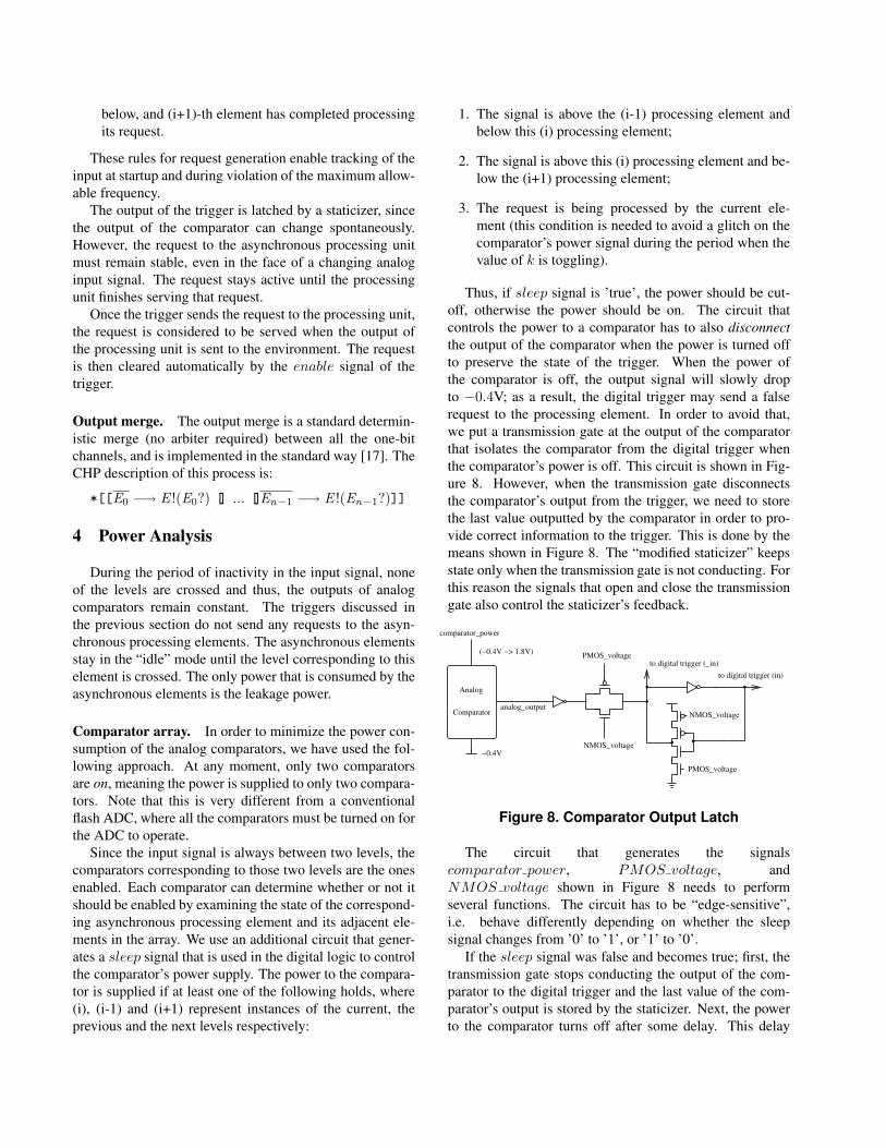
below, and (i+1)-th element has completed processingits request.
These rules for request generation enable tracking of theinput at startup and during violation of the maximum allow-able frequency.
The output of the trigger is latched by a staticizer, sincethe output of the comparator can change spontaneously.However, the request to the asynchronous processing unitmust remain stable, even in the face of a changing analoginput signal. The request stays active until the processingunit finishes serving that request.
Once the trigger sends the request to the processing unit,the request is considered to be served when the output ofthe processing unit is sent to the environment. The requestis then cleared automatically by the enable signal of thetrigger.
Output merge. The output merge is a standard determin-istic merge (no arbiter required) between all the one-bitchannels, and is implemented in the standard way [17]. TheCHP description of this process is:
*[[E0 −→ E !(E0?) [] ... []En−1 −→ E !(En−1?)]]
4 Power Analysis
During the period of inactivity in the input signal, noneof the levels are crossed and thus, the outputs of analogcomparators remain constant. The triggers discussed inthe previous section do not send any requests to the asyn-chronous processing elements. The asynchronous elementsstay in the “idle” mode until the level corresponding to thiselement is crossed. The only power that is consumed by theasynchronous elements is the leakage power.
Comparator array. In order to minimize the power con-sumption of the analog comparators, we have used the fol-lowing approach. At any moment, only two comparatorsare on, meaning the power is supplied to only two compara-tors. Note that this is very different from a conventionalflash ADC, where all the comparators must be turned on forthe ADC to operate.
Since the input signal is always between two levels, thecomparators corresponding to those two levels are the onesenabled. Each comparator can determine whether or not itshould be enabled by examining the state of the correspond-ing asynchronous processing element and its adjacent ele-ments in the array. We use an additional circuit that gener-ates a sleep signal that is used in the digital logic to controlthe comparator’s power supply. The power to the compara-tor is supplied if at least one of the following holds, where(i), (i-1) and (i+1) represent instances of the current, theprevious and the next levels respectively:
1. The signal is above the (i-1) processing element andbelow this (i) processing element;
2. The signal is above this (i) processing element and be-low the (i+1) processing element;
3. The request is being processed by the current ele-ment (this condition is needed to avoid a glitch on thecomparator’s power signal during the period when thevalue of k is toggling).
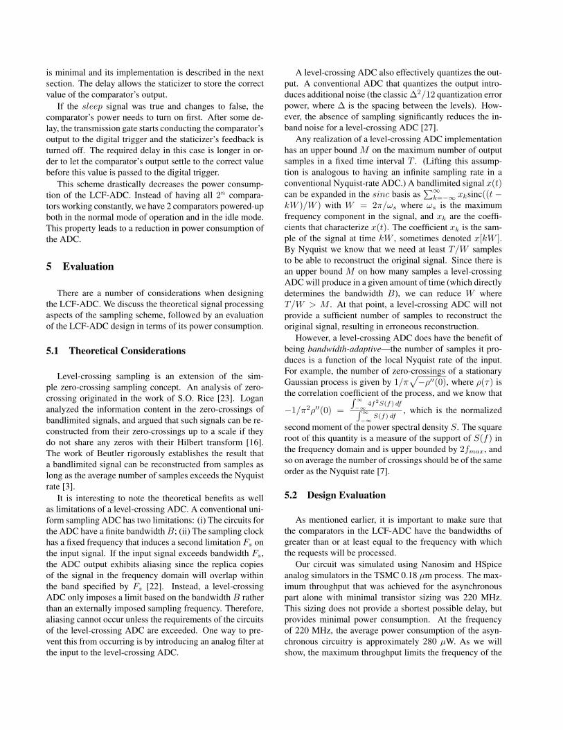
Thus, if sleep signal is ’true’, the power should be cut-off, otherwise the power should be on. The circuit thatcontrols the power to a comparator has to also disconnectthe output of the comparator when the power is turned offto preserve the state of the trigger. When the power ofthe comparator is off, the output signal will slowly dropto −0.4V; as a result, the digital trigger may send a falserequest to the processing element. In order to avoid that,we put a transmission gate at the output of the comparatorthat isolates the comparator from the digital trigger whenthe comparator’s power is off. This circuit is shown in Fig-ure 8. However, when the transmission gate disconnectsthe comparator’s output from the trigger, we need to storethe last value outputted by the comparator in order to pro-vide correct information to the trigger. This is done by themeans shown in Figure 8. The “modified staticizer” keepsstate only when the transmission gate is not conducting. Forthis reason the signals that open and close the transmissiongate also control the staticizer’s feedback.
comparator_power
analog_output
PMOS_voltage
NMOS_voltage
NMOS_voltage
PMOS_voltage
Analog
Comparator
−0.4V
(−0.4V −> 1.8V)
to digital trigger (in)
to digital trigger (_in)
Figure 8. Comparator Output Latch
The circuit that generates the signalscomparator power, PMOS voltage, andNMOS voltage shown in Figure 8 needs to performseveral functions. The circuit has to be “edge-sensitive”,i.e. behave differently depending on whether the sleepsignal changes from ’0’ to ’1’, or ’1’ to ’0’.
If the sleep signal was false and becomes true; first, thetransmission gate stops conducting the output of the com-parator to the digital trigger and the last value of the com-parator’s output is stored by the staticizer. Next, the powerto the comparator turns off after some delay. This delay
is minimal and its implementation is described in the nextsection. The delay allows the staticizer to store the correctvalue of the comparator’s output.
If the sleep signal was true and changes to false, thecomparator’s power needs to turn on first. After some de-lay, the transmission gate starts conducting the comparator’soutput to the digital trigger and the staticizer’s feedback isturned off. The required delay in this case is longer in or-der to let the comparator’s output settle to the correct valuebefore this value is passed to the digital trigger.
This scheme drastically decreases the power consump-tion of the LCF-ADC. Instead of having all 2n compara-tors working constantly, we have 2 comparators powered-upboth in the normal mode of operation and in the idle mode.This property leads to a reduction in power consumption ofthe ADC.
5 Evaluation
There are a number of considerations when designingthe LCF-ADC. We discuss the theoretical signal processingaspects of the sampling scheme, followed by an evaluationof the LCF-ADC design in terms of its power consumption.
5.1 Theoretical Considerations
Level-crossing sampling is an extension of the sim-ple zero-crossing sampling concept. An analysis of zero-crossing originated in the work of S.O. Rice [23]. Logananalyzed the information content in the zero-crossings ofbandlimited signals, and argued that such signals can be re-constructed from their zero-crossings up to a scale if theydo not share any zeros with their Hilbert transform [16].The work of Beutler rigorously establishes the result thata bandlimited signal can be reconstructed from samples aslong as the average number of samples exceeds the Nyquistrate [3].
It is interesting to note the theoretical benefits as wellas limitations of a level-crossing ADC. A conventional uni-form sampling ADC has two limitations: (i) The circuits forthe ADC have a finite bandwidth B; (ii) The sampling clockhas a fixed frequency that induces a second limitation Fs onthe input signal. If the input signal exceeds bandwidth Fs,the ADC output exhibits aliasing since the replica copiesof the signal in the frequency domain will overlap withinthe band specified by Fs [22]. Instead, a level-crossingADC only imposes a limit based on the bandwidth B ratherthan an externally imposed sampling frequency. Therefore,aliasing cannot occur unless the requirements of the circuitsof the level-crossing ADC are exceeded. One way to pre-vent this from occurring is by introducing an analog filter atthe input to the level-crossing ADC.
A level-crossing ADC also effectively quantizes the out-put. A conventional ADC that quantizes the output intro-duces additional noise (the classic ∆2/12 quantization errorpower, where ∆ is the spacing between the levels). How-ever, the absence of sampling significantly reduces the in-band noise for a level-crossing ADC [27].
Any realization of a level-crossing ADC implementationhas an upper bound M on the maximum number of outputsamples in a fixed time interval T . (Lifting this assump-tion is analogous to having an infinite sampling rate in aconventional Nyquist-rate ADC.) A bandlimited signal x(t)can be expanded in the sinc basis as
∑∞k=−∞ xksinc((t −
kW )/W ) with W = 2π/ωs where ωs is the maximumfrequency component in the signal, and xk are the coeffi-cients that characterize x(t). The coefficient xk is the sam-ple of the signal at time kW , sometimes denoted x[kW ].By Nyquist we know that we need at least T/W samplesto be able to reconstruct the original signal. Since there isan upper bound M on how many samples a level-crossingADC will produce in a given amount of time (which directlydetermines the bandwidth B), we can reduce W whereT/W > M . At that point, a level-crossing ADC will notprovide a sufficient number of samples to reconstruct theoriginal signal, resulting in erroneous reconstruction.
However, a level-crossing ADC does have the benefit ofbeing bandwidth-adaptive—the number of samples it pro-duces is a function of the local Nyquist rate of the input.For example, the number of zero-crossings of a stationaryGaussian process is given by 1/π
√−ρ′′(0), where ρ(τ) is
the correlation coefficient of the process, and we know that
−1/π2ρ′′(0) =
∫∞−∞
4f2S(f) df∫∞−∞
S(f) df, which is the normalized
second moment of the power spectral density S. The squareroot of this quantity is a measure of the support of S(f) inthe frequency domain and is upper bounded by 2fmax, andso on average the number of crossings should be of the sameorder as the Nyquist rate [7].
5.2 Design Evaluation
As mentioned earlier, it is important to make sure thatthe comparators in the LCF-ADC have the bandwidths ofgreater than or at least equal to the frequency with whichthe requests will be processed.
Our circuit was simulated using Nanosim and HSpiceanalog simulators in the TSMC 0.18 µm process. The max-imum throughput that was achieved for the asynchronouspart alone with minimal transistor sizing was 220 MHz.This sizing does not provide a shortest possible delay, butprovides minimal power consumption. At the frequencyof 220 MHz, the average power consumption of the asyn-chronous circuitry is approximately 280 µW. As we willshow, the maximum throughput limits the frequency of the
input signal. If desired, transistors can be resized for greaterperformance (higher throughput, smaller latency) at the ex-pense of higher power consumption. However, 220 MHz issufficient to meet our design requirements.
For a full swing signal, the maximum number of cross-ings that can be correctly interpreted by our LCF-ADC isdetermined by the signal bandwidth (BW ) and the maxi-mum throughput of the asynchronous circuitry (fmax):
BW · number of eventscycle
≤ fmax
Where the ’number of events’ represents the number ofcrossings, i.e. the number of requests issued to the asyn-chronous processing element by the digital trigger.
If we assume a full swing periodic input signal with 2ncrossings in one period (like a triangular wave or a sinu-soid), the equation becomes:
BW · 2n ≤ fmax
Thus, with fmax for minimal power consumption ataround 220MHz, the maximum number of levels that canbe correctly interpreted is:
n ≤ 110BW
with BW as the bandwidth of the input analog signal inMHz.
According to the above relationship, the maximum num-ber of reference levels that can still be properly interpretedby the converter with a full swing input signal of 1 MHz is110 levels, which corresponds to a 6 bit converter. If higherprecision in terms of the number of bits is desired, the speedof the asynchronous circuitry has to be increased.
In our simulations, the LCF-ADC was optimized for a 5MHz full swing input signal. In order to achieve this band-width and still have a short conversion time of the sample,the bias voltage of the comparators was set to the value of0.25 V. The delays in the logic that control the pass gateand the comparator power were implemented in the follow-ing way. The comparator power-off delay was implementedby two minimally sized inverters, because the required de-lay there is very short (just enough to disconnect the trans-mission gate and latch the correct value). However, the de-lay that controls the NMOS voltage and PMOS voltagesignals and allows the transmission gate to conduct, needsto be much longer. Once the power of the converter is on,sufficient time has to be given to the comparator in orderfor its output to settle to the correct value. This delay wasimplemented by an RC network. The delay at the chosenbias voltage is approximately 3 ns.
For all simulations a 4-bit converter (16 levels) was ex-amined (for comparison with the current topologies, how-ever this topology may be trivially extended to a higher-precision ADC). The layout area of the LCF-ADC increases
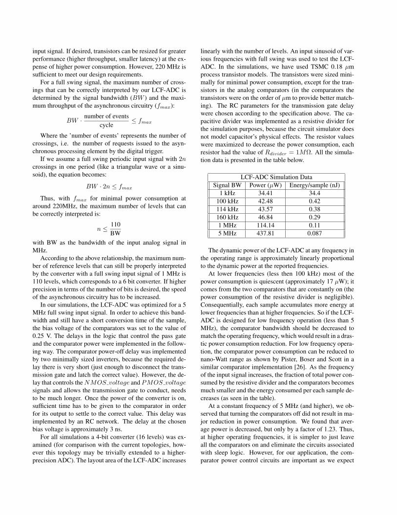
linearly with the number of levels. An input sinusoid of var-ious frequencies with full swing was used to test the LCF-ADC. In the simulations, we have used TSMC 0.18 µmprocess transistor models. The transistors were sized mini-mally for minimal power consumption, except for the tran-sistors in the analog comparators (in the comparators thetransistors were on the order of µm to provide better match-ing). The RC parameters for the transmission gate delaywere chosen according to the specification above. The ca-pacitive divider was implemented as a resistive divider forthe simulation purposes, because the circuit simulator doesnot model capacitor’s physical effects. The resistor valueswere maximized to decrease the power consumption, eachresistor had the value of Rdivider = 1MΩ. All the simula-tion data is presented in the table below.
LCF-ADC Simulation DataSignal BW Power (µW) Energy/sample (nJ)
1 kHz 34.41 34.4100 kHz 42.48 0.42114 kHz 43.57 0.38160 kHz 46.84 0.291 MHz 114.14 0.115 MHz 437.81 0.087
The dynamic power of the LCF-ADC at any frequency inthe operating range is approximately linearly proportionalto the dynamic power at the reported frequencies.
At lower frequencies (less then 100 kHz) most of thepower consumption is quiescent (approximately 17 µW); itcomes from the two comparators that are constantly on (thepower consumption of the resistive divider is negligible).Consequentially, each sample accumulates more energy atlower frequencies than at higher frequencies. So if the LCF-ADC is designed for low frequency operation (less than 5MHz), the comparator bandwidth should be decreased tomatch the operating frequency, which would result in a dras-tic power consumption reduction. For low frequency opera-tion, the comparator power consumption can be reduced tonano-Watt range as shown by Pister, Boser and Scott in asimilar comparator implementation [26]. As the frequencyof the input signal increases, the fraction of total power con-sumed by the resistive divider and the comparators becomesmuch smaller and the energy consumed per each sample de-creases (as seen in the table).
At a constant frequency of 5 MHz (and higher), we ob-served that turning the comparators off did not result in ma-jor reduction in power consumption. We found that aver-age power is decreased, but only by a factor of 1.23. Thus,at higher operating frequencies, it is simpler to just leaveall the comparators on and eliminate the circuits associatedwith sleep logic. However, for our application, the com-parator power control circuits are important as we expect
the ADC to be idle for significant periods of time.Renaudin came up with a different topology for an asyn-
chronous ADC. He has compared his A-ADC to the con-ventional synchronous ADCs [2]. The comparison (usinghis figure of merit) shows that his A-ADC is superior to allthe previous implementations. Here we present the com-parison of our ADC to Renaudin’s ADC, however the con-cept of SNR is not discussed since were are not reconstruct-ing the signal, and in our case the conventional SNR ex-pressions are not applicable. Since the signal is not re-constructed in our case we don’t make a direct compari-son between synchronous ADCs and LCF-ADC. The powerconsumption of an asynchronous level-crossing ADC de-signed using a successive-approximation topology by Re-naudin et al. (A-ADC) depends on the value of the up-down counter (from 0.898 mW to 1.603 mW in the idlemode) [2]. In our case the power consumption is alwaysthe same (at constant frequency input signal) and it is muchlower than the power of the A-ADC. Our average dynamicpower consumption is also significantly lower—the powerconsumed by the A-ADC is 1.716 mW. The maximum re-ported input signal bandwidth for the A-ADC is 114 kHz(hardware resolution is 4 bits). Our ADC simulations wereperformed with varying signal bandwidth (up to 5 MHz)with 4 bits of hardware resolution as well, and we use sig-nificantly less power than the A-ADC over the entire range.The A-ADC, however, was designed in a different fabri-cation technology (0.25 µm); however, a more recent ver-sion of the same architecture in 0.12 µm CMOS shows amaximum bandwidth of 160 kHz, and a power consump-tion of 180 µW, even though their results correspond to abetter fabrication technology [1]. An implementation sim-ilar to Renaudin’s A-ADC was presented by Shepard etal. [14, 15]; the power consumption was in the milli-Wattrange – higher then in Renaudin’s A-ADC. Lower powerconsumption in our ADC can be attributed to the architec-ture of the LCF-ADC, and the representation of the output.Note that associating a timestamp with the output wouldonly require an additional counter, which would not requiresignificant additional power [2] (approximately 15 µW).However, the data presented by Renaudin [1] is a result ofmeasurements, and all the data presented in this paper is aresult of simulations and will be confirmed after the LCF-ADC is fabricated.
6 Conclusions and Future Work
In this paper, we have described a new architecture forasynchronous analog-to-digital conversion. The configura-tion that was presented resembles a flash ADC, but usescompletely different digital processing circuits. In con-trast with a flash ADC that has all its comparators active,the LCF-ADC proposed here only has a fixed number (2)
of active comparators regardless of the hardware precisionof the ADC. Our design showed significant reduction inpower consumption compared to previously designed level-crossing asynchronous ADCs.
Our LCF-ADC can operate in the MHz regime (opti-mized for full swing input signals of 5 MHz frequency). Itcan also work at much higher frequencies with appropriatetransistor sizing at the cost of higher power consumption.The architecture also minimizes the transmission bandwidthby outputting only the increments or decrements of the in-put signal from the previous sample and not the completesample value (differential encoding). LCF-ADC enablesthe designers to perform further asynchronous signal pro-cessing (triggering, data collection and analysis) on an im-plicit representation of the input signal as a non-uniform intime sequence of bits. The applications of our LCF-ADCinclude embedded sensing systems, such as environmentalmonitoring applications and human body implants.
Future work could examine further reduction in powerconsumption of the comparators. We are also interested inthe design of circuits that operate directly on the implicitsignal representation to perform standard signal processingoperations.
Acknowledgments. We would like to thank Yannis Tsividisfor discussions on analog circuits and theoretical aspectsof continuous time analog-to-digital conversion, and AnnaScaglione for discussions on non-uniform sampling theory.This work was supported in part by the NSF under grantsITR 0428427 and NeTS 0435190.
A. Summary of CHP Notation
The CHP notation we use is based on Hoare’s CSP [6].A full description of CHP and its semantics can be foundin [21]. What follows is a short and informal description.
• Assignment: a := b. This statement means “assignthe value of b to a .” We also write a↑ for a := true,and a↓ for a := false .
• Selection: [G1 → S1 [] ... []Gn → Sn], where Gi’sare boolean expressions (guards) and Si’s are programparts. The execution of this command corresponds towaiting until one of the guards is true, and then exe-cuting one of the statements with a true guard. Thenotation [G] is short-hand for [G → skip], and de-notes waiting for the predicate G to become true. If theguards are not mutually exclusive, we use the verticalbar “|” instead of “[].”
• Repetition: *[G1 → S1 [] ... [] Gn → Sn]. Theexecution of this command corresponds to choosing
one of the true guards and executing the correspond-ing statement, repeating this until all guards evalu-ate to false . The notation *[S] is short-hand for*[true → S].
• Send: X !e means send the value of e over channel X .
• Receive: Y ?v means receive a value over channel Yand store it in variable v .
• Probe: The boolean expression X is true iff a com-munication over channel X can complete without sus-pending.
• Sequential Composition: S ;T
• Parallel Composition: S ‖ T or S ,T .
References
[1] E. Allier, J. Goulier, G. Sicard, A. Dezzani, E. Andre, andM. Renaudin. A 120nm low power asynchronous adc. InProceedings of ISLPED 2005, August 2005.
[2] E. Allier, G. Sicard, L. Fesquet, and M. Renaudin. A newclass of asynchronous A/D converters based on time quanti-zation. In Proceedings of the 9th Annual International Sym-posium on Asynchronous Circuits and Systems, pages 196–205, May 2003.
[3] F. Beutler. Error-free recovery of signals from irregularlyspaced samples. SIAM Review, 8(3), 1966.
[4] V. N. Ekanayake, C. Kelly IV, and R. Manohar. Bitsnap:Dynamic significance compression for a low-energy sensornetwork asynchronous processor. In Proceedings of the 11thIEEE International Symposium on Asynchronous Circuitsand Systems, pages 144–154, March 14-16 2005.
[5] R. Gregorian. Introduction to CMOS Op-Amps and Com-parators. John Wiley & Sons, 1999.
[6] C. A. R. Hoare. Communicating sequential processes. Com-munications of the ACM, 21(8):666–677, 1978.
[7] Yao-Win Hong, Anna Scaglione, and Rajit Manohar. Densesensor networks are also energy-efficient: When “more” is“less”. In Proceedings of MILCOM 2005, 2005.
[8] H. Inose, T. Aoki, and K. Watanabe. Asynchronous deltamodulation system. Electronics Letters, 2:95–96, 1966.
[9] P.G.A. Jespers. Integrated Converters, D to A and A to DArchitectures, Analysis and Simulation. Oxford UniversityPress, 2001.
[10] B. Kedem. Spectral analysis and discrimination by zero-crossings. Proceedings of the IEEE, 74(11):1477–1493,November 1986.
[11] B. Kedem. Time Series Analysis by Higher Order Crossings.IEEE Press, 1994.
[12] D. Kinnement and A. Yakovlev. Low power, low noise mi-cropipelined flash A-D converter. IEEE Proceedings on Cir-cuits Devices Systems, 146(5), 1999.
[13] D. Kinnement, A. Yakovlev, and B. Gao. Synchronous andasynchronous A/D conversion. IEEE Transactions on VLSISystems, 9(2), 2000.
[14] Y. W. Li, K. L. Shepard, and Y. P. Tsividis. Continuous-time digital signal processors. In Proceedings of the 11thAnnual International Symposium on Asynchronous Circuitsand Systems, New York City, USA, March 14-16 2005.
[15] Y. W. Li, K. L. Shepard, and Y. P. Tsividis. A continuous-time programmable digital fir filter. To be published in Jour-nal of Solid-State Circuits, 2005.
[16] B.F. Logan. Information in the zero crossings of bandpasssignals. Bell Systems Technical Journal, 56(4):487–510,April 1977.
[17] Rajit Manohar. Asynchronous VLSI systems. Class Notesfor ECE 574 at Cornell University, 1999.
[18] J. Mark and T. Todd. A nonuniform sampling approach todata compression. IEEE Transactions on Communications,COM-29(4), 1981.
[19] Alain J. Martin. Compiling communicating processes intodelay-insensitive VLSI circuits. Distributed Computing,1(4), 1986.
[20] Alain J. Martin. The limitations to delay-insensitivity inasynchronous circuits. In William J. Dally, editor, Proceed-ings of the 6th Conference on Advanced Research in VLSI,pages 263–278. MIT Press, 1990.
[21] Alain J. Martin. Programming in VLSI: From communicat-ing processes to delay-insensitive circuits. In C. A. R. Hoare,editor, Developments in Concurrency and Communication,UT Year of Programming Series, pages 1–64. Addison-Wesley, 1990.
[22] A. Oppenheim, A. Wilsky, and I. Young. Signals and Sys-tems. Prentice-Hall, 1995.
[23] S.O. Rice. Statistical properties of a sine wave plus randomnoise. Bell Systems Technical Journal, 27:109–157, January1948.
[24] J. Sauerbrey, D. Schmitt-Landsiedel, and R. Thewes. A0.5V, 1W successive approximation ADC. In ESSCIRC pro-ceedings, Firenze, Italy, September 24-26 2002.
[25] N. Sayiner, H. Sorensen, and T. Viswanathan. A level-crossing sampling scheme for A/D conversion. IEEE Trans-actions on Circuits and Systems II, 43(4), 1996.
[26] M. Scott, B. Boser, and K. Pister. An ultra low-power ADCfor distributed sensor networks. In ESSCIRC proceedings,Firenze, Italy, September 24-26 2002.
[27] Y. P. Tsividis. Digital signal processing in continuous time:a possibility for avoiding aliasing and reducing quantizationerror. In Proceedings of the International Conference onAcoustics, Speech, and Signal Processing, May 17-21 2004.

FURTHER READING
Click any one of the following links to be taken to a website which contains the following documents.
The following are some recent examples of Asynchronous ADC activity off the web.
6 bit Asynchronous December 2006Asynchronous ADC In CAD Mentor GraphicsAsynchronous Data Processing System ASYNCHRONOUS PARALLEL RESISTORLESS ADCFlash Asynchronous Analog-to-Digital ConverterNovel Asynchronous ADC ArchitectureLEVEL BASED SAMPLING FOR ENERGY CONSERVATION IN LARGE NETWORKSA Level-Crossing Flash Asynchronous Analog-to-Digital ConverterWeight functions for signal reconstruction based on level crossingsAdaptive Rate Filtering Technique Based on the Level Crossing SamplingAdaptive Level–Crossing Sampling Based DSP Systems A 0.8 V Asynchronous ADC for Energy Constrained Sensing Applications Spline-based signal reconstruction algorithm from multiple level crossing samplesA New Class of Asynchronous Analog-to-Digital ConvertersEffects of time quantization and noise in level crossing sampling stabilization
Here is some more background information on Analog to Digital converters.
A 1-GS/s 6-bit 6.7-mW ADCA Study of Folding and Interpolating ADCFolding_ADCs_Tutorialshigh speed ADC designInvestigation of a Parallel Resistorless ADC
Here are some patents on the subject.
4,291,299_Analog_to_digital_converter_using_timed4,352,999_Zero_crossing_comparators_with_threshold4,544,914_Asynchronously_controllable_successive_approximation4,558,348_Digital_video_signal_processing_system_using5,001,364_Threshold_crossing_detector5,315,284_Asynchronous_digital_threshold_detector_5,945,934_Tracking_analog_to_digital_converter6,020,840_Method_and_apparatus_for_representing_waveform6,492,929_Analogue_to_digital_converter_and_method6,501,412_Analog_to_digital_converter_including_a_quantizers6,667,707_Analog_to_digital_converter_with_asynchronous_ability6,720,901_Interpolation_circuit_having_a_conversio26,850,180_SelfTimed_ADC6,965,338_Cascade_A_D_converter7,133,791_Two_mean_level_crossing_time_interval
11.19.10_1.20PM [email protected] Sauer