a hybrid energy storage system using series-parallel recon ... - chia-hao... · doctor of...
TRANSCRIPT

A Hybrid Energy Storage System Using
Series-Parallel Reconfiguration Technique

A HYBRID ENERGY STORAGE SYSTEM USING
SERIES-PARALLEL RECONFIGURATION TECHNIQUE
BY
CHIA-HAO TU,
a thesis
submitted to the department of electrical & computer engineering
and the school of graduate studies
of mcmaster university
in partial fulfilment of the requirements
for the degree of
Doctor of Philosophy
c© Copyright by Chia-Hao Tu,
All Rights Reserved

Doctor of Philosophy (2015) McMaster University
(Electrical & Computer Engineering) Hamilton, Ontario, Canada
TITLE: A Hybrid Energy Storage System Using Series-Parallel
Reconfiguration Technique
AUTHOR: Chia-Hao Tu
B.Sc., (Electrical Engineering)
Illinois Institute of Technology, Chicago, U.S.A
SUPERVISOR: Dr. Ali Emadi
NUMBER OF PAGES: xvii, 185
ii
Abstract
Technology advancements enable and encourage higher system electrifications in var-
ious applications. More electrified applications need more capable and higher per-
forming sources of energy in terms of power delivery, power regeneration, and energy
capacity. For example, in electric, hybrid electric, and plug-in hybrid electric vehicle
applications (EVs, HEVs, and PHEVs), the power and energy ratings of the vehicle
energy storage system (ESS) have a direct impact on the vehicle performance. Many
researchers investigated and studied various aspects of hybrid energy storage systems
(HESS) wherein multiple ESSs are combined together to share system loads, increase
ESS capabilities, and cycle life. Various configurations and their application specific
topologies were also proposed by other researchers; the potential of HESS has been
proven to be very promising.
In this research, the goal is to present the theory of a HESS configuration that
has not been discovered thus far. This HESS configuration is called a series-parallel
reconfigurable HESS (SPR-HESS) since it is capable of recombining multiple storage
systems into different series, parallel, or series-parallel configurations, via power elec-
tronic converters, to accommodate different operation modes and load requirements.
Simulations, as well as experimental verifications, are presented in this thesis.
iii

Acknowledgments
I would like to thank Dr. Emadi, my advisor, for his support in many forms. I
would also like to thank Dr. Schofield, Dr. Reilly, and Dr. Perez-Pinal for providing
feedback and comments on my research throughout the past supervisory committee
meetings.
This research was undertaken, in part, thanks to funding from the Canada Excel-
lence Research Chairs Program.
iv

Notation and abbreviations
BMS: Battery Management System
VMS: Votlage Management System
PCB: Printed Circuit Board
PEC: Power Electronics Converter
UC: Ultracapcacitor
ESS: Energy Storage System
HESS: Hybrid Energy Storage System
SPR-HESS: Series-Parallel Reconfigurable Hybrid Energy Storage System
BFL: Battery facing the load
UCFL: Ultracapacitor facing the load
KVL: Kirchhoff’s Voltage Law
KCL: Kirchhoff’s Current Law
SoC: State of Charge
CC: Constant Current
CV: Constant Voltage
Vmin: Minimum voltage
Vmax: Maximum voltage
VBatt,min: Minimum battery voltage
v

VBatt,max: Maximum battery voltage
VUC,min: Minimum UC voltage
VUC,max: Maximum UC voltage
PBatt: Battery power
PUC : Ultracapacitor power
PLoad: Load power
PSource: Source power
ηBatt: Battery efficiency
ηUC : UC efficiency
ηComp: Component efficiency
ηPEC : PEC efficiency
ηPEC1: PEC1 efficiency
ηPEC2: PEC2 efficiency
vin: Input voltage
Vin: Large signal input voltage
vin: Small signal input voltage
vL: Inductor voltage
VL: Large signal inductor voltage
vL: Small signal inductor voltage
vC : Capacitor voltage
VC : Large signal capacitor voltage
vC : Small signal capacitor voltage
VC(s): Small signal capacitor voltage in s-domain
vUC : Ultracapacitor voltage
vi

VUC : Large signal ultracapacitor voltage
vUC : Small signal ultracapacitor voltage
VUC(s): Small signal ultracapacitor voltage in s-domain
vB: Battery voltage
VB: Large signal battery voltage
vB: Small signal battery voltage
iin: Input current
Iin: Large signal input current
iin: Small signal input current
iL: Inductor current
IL: Large signal inductor current
iL: Small signal inductor current
IL(s): Small signal inductor current in s-domain
iC : Capacitor current
IC : Large signal capacitor current
iC : Small signal capacitor current
iUC : Ultracapacitor current
IUC : Large signal ultracapacitor current
iUC : Small signal ultracapacitor current
iB: Battery current
IB: Large signal battery current
iB: Small signal battery current
iB(s): Small signal battery current in s-domain
iLoad: Load current
vii

ILoad: Large signal load current
RB: Battery internal resistance
RUC : Ultracapacitor internal resistance
RLoad: Load resistance
L: Inductance
C: Capacitance
d: Duty cycle
D: Large signal duty cycle
d: Small signal duty cycle
d(s): Small signal duty cycle in s-domain
T: Switching period
viii

Contents
Abstract iii
Acknowledgments iv
Notation and abbreviations v
1 Introduction 1
1.1 Introduction . . . . . . . . . . . . . . . . . . . . . . . . . . . . . . . . 1
1.2 Research Goals and Motivations . . . . . . . . . . . . . . . . . . . . . 3
1.3 Thesis Overview . . . . . . . . . . . . . . . . . . . . . . . . . . . . . . 5
2 Introduction to Cell Equalization Methods 6
2.1 Introduction . . . . . . . . . . . . . . . . . . . . . . . . . . . . . . . . 6
2.2 Battery Management Systems . . . . . . . . . . . . . . . . . . . . . . 7
2.3 Dissipative Cell Equalization Method and Examples . . . . . . . . . . 11
2.3.1 Dissipative Resistor Method . . . . . . . . . . . . . . . . . . . 11
2.3.2 Dissipative Power Switch Method . . . . . . . . . . . . . . . . 12
2.4 Non-dissipative Cell Equalization Method and Examples . . . . . . . 14
2.4.1 Shunting Method . . . . . . . . . . . . . . . . . . . . . . . . . 14
ix

2.4.2 Inductive Shuttling Method . . . . . . . . . . . . . . . . . . . 15
2.4.3 Capacitive Shuttling Method 1 . . . . . . . . . . . . . . . . . 17
2.4.4 Capacitive Shuttling Method 2 . . . . . . . . . . . . . . . . . 19
2.4.5 Pack-to-cell Method with Flyback Converter . . . . . . . . . . 20
2.4.6 Pack-to-cell Method with Ramp Converter . . . . . . . . . . . 22
2.5 Summary . . . . . . . . . . . . . . . . . . . . . . . . . . . . . . . . . 24
3 Fundamentals of Hybrid Energy Storage Systems 25
3.1 Introduction . . . . . . . . . . . . . . . . . . . . . . . . . . . . . . . . 25
3.2 Power Flow Efficiency and UC Energy Utilization of HESS Configurations 26
3.3 Direct Parallel Connected Configuration . . . . . . . . . . . . . . . . 27
3.4 Cascaded Configuration Using One Power Electronic Converter . . . . 31
3.5 Cascaded Configuration Using Two Power Electronics Converters . . 35
3.6 Parallel-Connected Output Configuration . . . . . . . . . . . . . . . . 38
3.7 Active Coupling Configuration Using a Multi-input Power Electronics
Converter . . . . . . . . . . . . . . . . . . . . . . . . . . . . . . . . . 40
3.8 Summary . . . . . . . . . . . . . . . . . . . . . . . . . . . . . . . . . 42
4 Series-Parallel Reconfigurable Hybrid Energy Storage Systems 43
4.1 Introduction . . . . . . . . . . . . . . . . . . . . . . . . . . . . . . . . 43
4.2 Series-Parallel Shifting of Energy Storage Systems . . . . . . . . . . . 44
4.3 Introduction to a Hybrid Energy Storage System Utilizing Series-Parallel
Reconfiguration Technique . . . . . . . . . . . . . . . . . . . . . . . . 46
4.4 Theoretical System Level Operation Modes . . . . . . . . . . . . . . . 49
4.4.1 Mode 1 . . . . . . . . . . . . . . . . . . . . . . . . . . . . . . 49
x

4.4.2 Mode 2 . . . . . . . . . . . . . . . . . . . . . . . . . . . . . . 49
4.4.3 Mode 3 . . . . . . . . . . . . . . . . . . . . . . . . . . . . . . 50
4.4.4 Mode 4 . . . . . . . . . . . . . . . . . . . . . . . . . . . . . . 50
4.4.5 Mode 5 . . . . . . . . . . . . . . . . . . . . . . . . . . . . . . 50
4.5 Power Flow Efficiency and UC Energy Utilization of HESS Configura-
tion Using Series-Parallel Reconfigurable Technique . . . . . . . . . . 51
4.6 Comparative Analysis . . . . . . . . . . . . . . . . . . . . . . . . . . 53
4.7 Design Considerations and Limitations of SPR-HESS . . . . . . . . . 56
4.8 Summary . . . . . . . . . . . . . . . . . . . . . . . . . . . . . . . . . 57
5 Simulation and Case Study of a Series-Parallel Reconfigurable Hy-
brid Energy Storage System Topology 58
5.1 Introduction . . . . . . . . . . . . . . . . . . . . . . . . . . . . . . . . 58
5.2 Description of Topology Operation Modes . . . . . . . . . . . . . . . 59
5.2.1 Mode 1 . . . . . . . . . . . . . . . . . . . . . . . . . . . . . . 61
5.2.2 Mode 2 . . . . . . . . . . . . . . . . . . . . . . . . . . . . . . 64
5.2.3 Mode 3 . . . . . . . . . . . . . . . . . . . . . . . . . . . . . . 65
5.2.4 Mode 4 . . . . . . . . . . . . . . . . . . . . . . . . . . . . . . 71
5.2.5 Mode 5 . . . . . . . . . . . . . . . . . . . . . . . . . . . . . . 74
5.3 Power Management and Control Strategy . . . . . . . . . . . . . . . . 77
5.3.1 Control Strategy 1 - UC Sustaining Mode . . . . . . . . . . . 77
5.3.2 Control Strategy 2 - UC Depletion Mode . . . . . . . . . . . . 79
5.3.3 Special Modes . . . . . . . . . . . . . . . . . . . . . . . . . . . 81
5.4 Description of System Analytical Model . . . . . . . . . . . . . . . . 82
5.4.1 Buck Mode . . . . . . . . . . . . . . . . . . . . . . . . . . . . 83
xi

5.4.2 Boost Mode . . . . . . . . . . . . . . . . . . . . . . . . . . . . 92
5.4.3 Buck-Boost Mode . . . . . . . . . . . . . . . . . . . . . . . . . 99
5.5 Simulation Setup . . . . . . . . . . . . . . . . . . . . . . . . . . . . . 121
5.5.1 Simulation Parameters and Specifications . . . . . . . . . . . . 121
5.5.2 Simulation Model and Control Strategy Logics . . . . . . . . . 123
5.6 Simulation Results and Discussion . . . . . . . . . . . . . . . . . . . . 129
5.6.1 Simulation Results of PEC Functionalities . . . . . . . . . . . 129
5.6.2 Simulation Results of SPR-HESS used for UDDS Drive Cycle
with Different Control Strategies . . . . . . . . . . . . . . . . 133
5.6.3 Comparative Analysis via Simulation . . . . . . . . . . . . . . 146
5.7 Summary . . . . . . . . . . . . . . . . . . . . . . . . . . . . . . . . . 152
6 Experimental Setup and Results 154
6.1 Introduction . . . . . . . . . . . . . . . . . . . . . . . . . . . . . . . . 154
6.2 Experimental Setup Design and Implementation . . . . . . . . . . . . 154
6.2.1 Power Electronics Converter . . . . . . . . . . . . . . . . . . . 154
6.2.2 Accumulator Selection and Design . . . . . . . . . . . . . . . . 157
6.3 Experimental Results and Discussion . . . . . . . . . . . . . . . . . . 159
6.4 Summary . . . . . . . . . . . . . . . . . . . . . . . . . . . . . . . . . 167
7 Conclusion 169
xii

List of Figures
1.1 Comparative ragone plot amongst selected lithium battery and UC cells. 3
2.1 Series connected battery cells with different SOC. . . . . . . . . . . . 8
2.2 An example of a battery management system setup. . . . . . . . . . . 10
2.3 An example of a cell equalizer setup using dissipative resistors. . . . . 11
2.4 An example of a cell equalizer setup using dissipative power switches. 13
2.5 An example of a cell equalizer setup using shunting method. . . . . . 15
2.6 An example of a cell equalizer setup using inductive shuttling method. 16
2.7 An example of a cell equalizer setup using capacitive shuttling method 1. 18
2.8 An example of a cell equalizer setup using capacitive shuttling method 2. 19
2.9 An example of a cell equalizer setup using a flyback converter. . . . . 21
2.10 An example of a cell equalizer setup using a ramp converter. . . . . . 23
3.1 Direct parallel connected HESS configuration. . . . . . . . . . . . . . 28
3.2 Battery and UC HESS with direct parallel connected configuration. . 28
3.3 Example HESS topology [39]. . . . . . . . . . . . . . . . . . . . . . . 29
3.4 Example HESS topology [46]. . . . . . . . . . . . . . . . . . . . . . . 30
3.5 Powertrain topology used in [46]. . . . . . . . . . . . . . . . . . . . . 30
3.6 Cascaded HESS configuration with one PEC. . . . . . . . . . . . . . . 31
xiii

3.7 Battery and UC HESS with cascaded connected configuration with one
PEC. . . . . . . . . . . . . . . . . . . . . . . . . . . . . . . . . . . . . 32
3.8 Example HESS topology [9]. . . . . . . . . . . . . . . . . . . . . . . . 33
3.9 Example HESS topology [38]. . . . . . . . . . . . . . . . . . . . . . . 34
3.10 Example HESS topology [22,23]. . . . . . . . . . . . . . . . . . . . . 35
3.11 Cascaded HESS configuration with two PECs. . . . . . . . . . . . . . 36
3.12 Battery and UC HESS with cascaded connected configuration using
two PECs. . . . . . . . . . . . . . . . . . . . . . . . . . . . . . . . . . 36
3.13 Example HESS topology [53]. . . . . . . . . . . . . . . . . . . . . . . 38
3.14 Parallel-connected output HESS configuration. . . . . . . . . . . . . . 38
3.15 Battery and UC HESS with parallel-connected output configuration. . 39
3.16 Example HESS topology [15]. . . . . . . . . . . . . . . . . . . . . . . 40
3.17 HESS configuration with a multi-input PEC. . . . . . . . . . . . . . . 41
3.18 Battery and UC HESS with active coupling configuration using a multi-
input PEC. . . . . . . . . . . . . . . . . . . . . . . . . . . . . . . . . 41
3.19 Example HESS topology [54]. . . . . . . . . . . . . . . . . . . . . . . 42
4.1 Capacitor changeover circuits . . . . . . . . . . . . . . . . . . . . . . 45
4.2 HESS topology with changeover circuit for UC. . . . . . . . . . . . . 46
4.3 SPR-HESS general forms. . . . . . . . . . . . . . . . . . . . . . . . . 48
4.4 System level operation modes (UCFL). . . . . . . . . . . . . . . . . . 51
4.5 Battery and UC HESS with series-parallel reconfigurable configuration. 52
5.1 Conceptual implementation 1. . . . . . . . . . . . . . . . . . . . . . . 59
5.2 Different types of bi-directional switches. . . . . . . . . . . . . . . . . 60
5.3 Conceptual implementation 2. . . . . . . . . . . . . . . . . . . . . . . 61
xiv

5.4 Mode 1. . . . . . . . . . . . . . . . . . . . . . . . . . . . . . . . . . . 63
5.5 Mode 2. . . . . . . . . . . . . . . . . . . . . . . . . . . . . . . . . . . 64
5.6 Mode 3 variation a - boost or buck modes. . . . . . . . . . . . . . . . 66
5.7 Mode 3 variation a - direct modes. . . . . . . . . . . . . . . . . . . . 67
5.8 Mode 3 variation b. . . . . . . . . . . . . . . . . . . . . . . . . . . . . 69
5.9 Mode 4. . . . . . . . . . . . . . . . . . . . . . . . . . . . . . . . . . . 72
5.10 Mode 5. . . . . . . . . . . . . . . . . . . . . . . . . . . . . . . . . . . 75
5.11 Example power management for control strategy - ultracapacitor sus-
taining mode. . . . . . . . . . . . . . . . . . . . . . . . . . . . . . . . 79
5.12 Example power management for control strategy - UC depletion mode. 80
5.13 Buck mode circuit. . . . . . . . . . . . . . . . . . . . . . . . . . . . . 84
5.14 Buck mode equivalent circuit for the switch closed. . . . . . . . . . . 84
5.15 Buck mode equivalent circuit for the switch open. . . . . . . . . . . . 85
5.16 Boost mode circuit. . . . . . . . . . . . . . . . . . . . . . . . . . . . . 93
5.17 Boost mode equivalent circuit for the switch closed. . . . . . . . . . . 93
5.18 Boost mode equivalent circuit for the switch open. . . . . . . . . . . . 94
5.19 Buck-boost mode circuit - variation 1. . . . . . . . . . . . . . . . . . 101
5.20 Buck-boost mode equivalent circuit for the switch closed - variation 1. 101
5.21 Buck-boost mode equivalent circuit for the switch open - variation 1. 102
5.22 Buck-boost mode circuit - variation 2. . . . . . . . . . . . . . . . . . 107
5.23 Buck-boost mode equivalent circuit for the switch closed - variation 2. 107
5.24 Buck-boost mode equivalent circuit for the switch open - variation 2. 109
5.25 Buck-boost mode circuit - variation 3. . . . . . . . . . . . . . . . . . 114
5.26 Buck-boost mode equivalent circuit for the switch closed - variation 3. 115
xv

5.27 Buck-boost mode equivalent circuit for the switch open - variation 3. 116
5.28 Autonomie Simulation Model. . . . . . . . . . . . . . . . . . . . . . . 123
5.29 Urban Dynamometer Driving Schedule (UDDS) Power and Speed Profile.124
5.30 Simulink Simulation Model for Drive Cycle Simulations. . . . . . . . 125
5.31 State-flow Control Logic for UC Sustaining Mode. . . . . . . . . . . . 125
5.32 State-flow Control Logic for UC Depletion Mode. . . . . . . . . . . . 126
5.33 Simulink Simulation Model for PEC in Buck Mode. . . . . . . . . . . 127
5.34 Simulink Simulation Mode for PEC in Boost Mode. . . . . . . . . . . 127
5.35 Simulink Simulation Model for PEC in Buck-boost Mode Variation 1. 128
5.36 Simulink Simulation Model for PEC in Buck-boost Mode Variation 2. 128
5.37 Simulink Simulation Model for PEC in Buck-boost Mode Variation 3. 129
5.38 PEC Simulation Result - Buck Mode. . . . . . . . . . . . . . . . . . . 130
5.39 PEC Simulation Result - Boost Mode. . . . . . . . . . . . . . . . . . 131
5.40 PEC Simulation Result - Buck-boost Mode v1. . . . . . . . . . . . . . 131
5.41 PEC Simulation Result - Buck-boost Mode v2. . . . . . . . . . . . . . 132
5.42 PEC Simulation Result - Buck-boost Mode v3. . . . . . . . . . . . . . 133
5.43 Drive Cycle Simulation Current Plots using UC Sustaining. . . . . . . 135
5.44 Drive Cycle Simulation Power Plots using UC Sustaining. . . . . . . . 136
5.45 Drive Cycle Simulation Voltage Plots using UC Sustaining. . . . . . . 137
5.46 Drive Cycle Simulation Current Plots using UC Depletion. . . . . . . 139
5.47 Drive Cycle Simulation Power Plots using UC Depletion. . . . . . . . 140
5.48 Drive Cycle Simulation Voltage Plots using UC Depletion. . . . . . . 141
5.49 Drive Cycle Simulation Current Plots using Mixed Mode. . . . . . . . 143
5.50 Drive Cycle Simulation Power Plots using Mixed Mode. . . . . . . . . 144
xvi

5.51 Drive Cycle Simulation Voltage Plots using Mixed Mode. . . . . . . . 145
5.52 Comparative Chart - Battery Charg-/Discharging Rates. . . . . . . . 146
5.53 Comparative Chart - Maximum Discharging Power. . . . . . . . . . . 148
5.54 Comparative Chart - Maximum Charging Power. . . . . . . . . . . . 149
5.55 Comparative Chart - Battery Remaining SOC After 1 Simulation Cycle.150
5.56 Voltage level comparison of SPR-HESS UCFL, BFL, and adjusted BFL
under mixed control strategy mode. . . . . . . . . . . . . . . . . . . . 152
6.1 PEC design and implementation. . . . . . . . . . . . . . . . . . . . . 156
6.2 UC pack design and implementation. . . . . . . . . . . . . . . . . . . 158
6.3 Experimental setup. . . . . . . . . . . . . . . . . . . . . . . . . . . . 159
6.4 Screen capture of operation mode M1a - No load, battery charging UC,
buck-boost mode. . . . . . . . . . . . . . . . . . . . . . . . . . . . . . 160
6.5 Screen captures of operation mode M3a-1 - Battery only, boost mode. 161
6.6 Screen capture of operation mode M3a-3 - Battery only, direct mode. 162
6.7 Screen captures of operation mode M3b-1 - Battery only, buck-boost
mode. . . . . . . . . . . . . . . . . . . . . . . . . . . . . . . . . . . . 163
6.8 Screen captures of operation mode M4-1 - Battery // UC, buck-boost
mode - Load sharing operation. . . . . . . . . . . . . . . . . . . . . . 165
6.9 Screen captures of operation mode M4-1 - Battery // UC, buck-boost
mode - UC charge sustaining operation. . . . . . . . . . . . . . . . . . 166
6.10 Screen capture of operation modes M3a-1 and M5 - Battery only, boost
mode and battery + UC, direct series mode. . . . . . . . . . . . . . . 167
xvii

Chapter 1
Introduction
1.1 Introduction
In advanced electrified applications such as EV, HEV, and PHEV, the energy storage
system (ESS) power and energy density and rating have a direct impact on the ve-
hicle performance: regenerative braking, acceleration, and cruising. In regenerative
braking mode, the ESS has to be able to withstand surge charges. In the accelera-
tion mode, the ESS has to supply a high amount of power. In cruising mode, ESS
must be able to maintain its charge long enough for the operation time [23]. Battery
has high energy density, but regenerative braking induces random charging to the
battery, and that causes a decrease in battery life. Although there are batteries that
have higher power density, they are expensive and introduce temperature manage-
ment issues that require using advanced water cooling or climate control [29]. Besides
the cost and temperature management issues, to have a battery cell performing up
to its limit within a pack, all the cells in the pack have to be balanced or have to
have similar performance parameters in terms of the capacity, internal resistance,
1

Ph.D. Thesis - Chia-Hao Tu McMaster - Electrical Engineering
and self-discharging rate. As a result, this involves having advanced battery manage-
ment system or selectively grouping cells that have similar performance parameters
from a batch of cells; in both cases, cost and complexity are increased [9]. Moreover,
because of the Peukerts effect, battery losses its capacity at a higher discharging
rate [11,23,25,59,69]. It is an ongoing challenge to have a single type of ESS that can
have high energy, high power, and long cycle life. Thus, researchers propose combin-
ing ultra-capacitor (UC) with battery, hence hybrid energy storage system (HESS),
to handle the surge power to increase battery life [9,20,23,59,69]. Figure 1.1 shows a
comparative Ragone plot with several selected lithium battery and UC cells that are
available in the market. Lithium battery cells, in general, have much higher specific
energy than UC cells, though some can produce higher discharging power that is
equivalent to those produced by UC cells. On the other hand, although UC cells have
much lower specific energy than battery cells, they have much higher specific power
than the normal battery cells. By combining energy types of ESS, such as internal
combustion engine-generator set (ICE-GEN) with fossil fuel tank, battery, and fuel
cell (FC) with hydrogen fuel tank, with power types, such as an UC, one can utilize
the inherent strengths of each individual system to optimize efficiency, cycle life, and
overall system simplicity.
2

Ph.D. Thesis - Chia-Hao Tu McMaster - Electrical Engineering
Figure 1.1: Comparative ragone plot amongst selected lithium battery and UC cells.
1.2 Research Goals and Motivations
Though UC has high power density and depth of discharge in return of having low
energy density, UCs voltage level fluctuates greatly during charging and discharging
due to the linear relationship between the change of capacitor current and the change
of voltage. Therefore, it gets more difficult to harvest a UC’s energy and power at
its lower operating voltage level. One can use power electronics converters (PECs) to
regulate the power and output voltage of the UC bank; this method is popular and
3
Ph.D. Thesis - Chia-Hao Tu McMaster - Electrical Engineering
is the foundation of all the previously proposed HESS configurations and topologies
by other researchers. However, PECs have their limits and 100% energy utilization
of the UC bank is not practical using solely the PEC method. Another way to do so
is to use parallel-series shifting circuits that can reconfigure UC cells in a whole bank
to further increase energy utilization and its efficiency [18,70].
Even though UC has higher charge/discharge efficiency, higher power density,
and higher cycle life than that of the battery, reference [22] shows that the increased
capital cost, PEC, and system complexity of introducing an additional UC bank to
an ESS might not be justified by the overall increase in battery life, efficiency, and
ESS power density. Life-cycle cost (dollar per kilometer) is also considered, and the
author concluded that HESS is not viable when life-cycle cost is taken into account.
The scope of this research does not cover the cost effectiveness of the HESS as such
challenge will be resolved gradually in the future due to technology advancement,
discoveries of new material composites, and high market demands.
No HESS configuration presented thus far has considered a HESS variant using
parallel-series reconfiguration (SPR) technique, which adapt new concepts and ap-
proaches to combine multiple ESSs by rearranging them into series, parallel, and
series-parallel configurations to satisfy the load requirements. This HESS can work
with any kind of ESS, such as a battery, a UC, a fuel cell, and an ICE-GEN. Although
the HESS can be used for different applications, this research focuses on the func-
tionalities of the new kind of HESS, SPR-HESS, that primarily consists of battery
and UC.
4

Ph.D. Thesis - Chia-Hao Tu McMaster - Electrical Engineering
1.3 Thesis Overview
In chapter 2, battery management systems and cell equalization methods are in-
troduced and discussed. These methods and systems are needed to address the
performance and safety issues that occur from power cycling series-connected cells
throughout the operating life-cycle.
In chapter 3, five fundamental HESS configurations are introduced followed by
several example topologies proposed by other researchers to implement them in vari-
ous applications.
In chapter 4, SPR-HESS configuration is introduced. Its theoretical operation
modes are described in details. Then, a comparative analysis based on power flow
efficiency and energy utilization from the system point-of-view amongst the afore-
mentioned five HESS configurations and SPR-HESS is discussed.
In chapter 5, a topology that is designed to implement the SPR-HESS configura-
tion is presented with its detailed operation modes, switching tables, example power
management and control strategies, circuit analysis of three distinct PEC modes, and
simulation studies. Then, the aforementioned comparative analysis in chapter 4 is
revisited and done via simulations to observe the differences and similarities amongst
the different HESS topologies.
In chapter 6, experimental setup of the presented SPR-HESS topology in chapter
5 is described. Then, experimental verifications of the functionalities of the topology
are presented.
Lastly, in chapter 7, the research summary, conclusion, and potential future work
are presented to sum up the dissertation.
5

Chapter 2
Introduction to Cell Equalization
Methods
2.1 Introduction
Ever-growing technological advancement enables higher electrifications to unlock higher
performance and capabilities in various applications; higher electrification requires
larger, more efficient, and more capable energy sources. In many applications, one of
the requirements for energy sources, aside from having high power and energy capac-
ity, is high source voltage level. Energy cells have to be stacked together in series in
order to provide higher voltage level. The trade-offs for connecting energy cells in se-
ries are that the individual cell voltage level varies over time due to even the slightest
variations and imbalances amongst the cells and the entire string of energy cells has
no fault tolerance itself and is subject to single point of failure. There are cases of
ESS failures in various industries. For instance, Cessna had to replace CJ4’s lithium-
ion batteries with other types of batteries because of a fire incident that broke out
6

Ph.D. Thesis - Chia-Hao Tu McMaster - Electrical Engineering
while charging its lithium-ion system [28]. Boeing 787 Dreamliner also had lithium-
ion battery failures in 2013 and was forced to make emergency landings [41, 58, 68].
On the other hand, automotive industry too had their share of incidents involving
lithium-ion battery technology. For example, there was a reported incident where
Chevrolet Volt’s lithium-ion battery system caught fire due to a leakage in its cooling
system from a crash test [66]. Therefore, extra precautions in ESS design, manage-
ment systems, and equalization circuits are needed, especially for advanced energy
cells such as lithium-ion batteries and UCs.
2.2 Battery Management Systems
In applications such as electrified vehicles, ESS cells are often connected in series and
parallel strings to make up the entire ESS banks for the systems. Because of the load
demands of higher voltage sources, battery cells need to be connected in series in
order to meet the requirements of the systems. However, due to having different cell
self-discharge rate and capacity of different battery cells, by connecting battery cells
in series and cycling power through them, the SoC differences amongst the battery
cells would gradually worsen and cause performance and safety issues. For example,
figure 2.1a shows three battery cells that are connected in series, and figure 2.1b
shows how these three battery cells, without having any balancing system, can have
different SoC after a period of time. As a result, during a charging operation, B1
is the limiting battery cell because it would be fully charged first. Because all the
cells are connected in series, the charger has to stop charging the battery string, as
a result, leaving B2 and B3 not fully charged, otherwise B1 has the risk of being
over-charged. On the other hand, during discharging operation, B3 is the limiting
7

Ph.D. Thesis - Chia-Hao Tu McMaster - Electrical Engineering
battery cell because it would reach the minimum SoC limit first before the other cells
do, resulting in lower overall system performance because B1 and B2 still have more
charges to provide to the system but unable to do so.
(a) Battery string. (b) Individual battery cell SOC.
Figure 2.1: Series connected battery cells with different SOC.
Moreover, by connecting battery cells in series, any single point failure within the
battery string can put the entire system out of service. Therefore, it is important to
implement battery management systems that can monitor and protect the battery
cells and the systems around them, thus, prolonging overall system life [8, 11,34].
A typical battery management system consists of various sensors like voltage,
temperature, and current, safety relay controllers that can engage and disengage
the battery bank from the system, and communication peripherals to communicate
with higher-level control systems; figure 2.2 shows an example of a BMS setup. A
BMS monitors the states of the battery cells such as the temperature, SoC, volt-
age, and current and uses the information to protect the battery cells as well as
systems around them from hazardous conditions such as under-charge, over-charge,
8

Ph.D. Thesis - Chia-Hao Tu McMaster - Electrical Engineering
over-current, under-temp, and over-temp. The main feature of a BMS is cell balanc-
ing/equalization that equalizes the battery cell charges using different cell equalization
methods which, in general, can be categorized into two major methods; one is dissipa-
tive, and another one is non-dissipative method. In the rest of this chapter, dissipative
and non-dissipative methods as well as several examples of cell equalization topologies
are discussed.
9

Ph.D. Thesis - Chia-Hao Tu McMaster - Electrical Engineering
Figure 2.2: An example of a battery management system setup.
10

Ph.D. Thesis - Chia-Hao Tu McMaster - Electrical Engineering
2.3 Dissipative Cell Equalization Method and Ex-
amples
For dissipative cell equalization method, energy is discharged from cells that have
higher charges so that their SoC match the weaker cells.
2.3.1 Dissipative Resistor Method
Figure 2.3 shows a cell equalizer using dissipative resistor method [5,6,34]. As shown
in the figure, each battery cell has its own discharging circuit with a power resistor
as the dissipative component. When more charged cells are detected, the controller
turns on their corresponding switches to discharge them through the power resistors.
Figure 2.3: An example of a cell equalizer setup using dissipative resistors.
11

Ph.D. Thesis - Chia-Hao Tu McMaster - Electrical Engineering
Dissipative resistor method operates during charging of the ESS; it is relatively
simple to implement and required simple cooling systems such as passive cooling; so
it is suitable for smaller applications such as laptops and cell phones that have size
limits. However, because of the inefficiency due to the cell energy being discharged
in the dissipative resistors and the heat being generated proportional to the size of
the ESS being balanced, it is not scalable for larger applications such as electrified
vehicles.
2.3.2 Dissipative Power Switch Method
Figure 2.4 shows a cell equalizer using dissipative power switch method [27]. Similar
to the previous example of using power resistors as dissipative elements, in this case,
power switches are used as the dissipative components. Also similar to the previous
example, each battery cell has its own discharging circuit with a power switch, and in
this case analog circuits are used to turn on and off the power switches for discharging
overcharged battery cells.
12

Ph.D. Thesis - Chia-Hao Tu McMaster - Electrical Engineering
Figure 2.4: An example of a cell equalizer setup using dissipative power switches.
Compared to the dissipative resistor method, dissipative power switch method
is more modular and simpler to implement; fewer sensors and control circuits are
required. However, this method has the same disadvantages as the dissipative resistor
method, therefore, it is suitable only for small applications because of low efficiency.
13

Ph.D. Thesis - Chia-Hao Tu McMaster - Electrical Engineering
2.4 Non-dissipative Cell Equalization Method and
Examples
For non-dissipative cell equalization, energy is transferred from cells that have the
higher charge to weaker cells for balancing. Comparing with a dissipative meth-
ods, a non-dissipative method is more efficient, however, it typically requires more
components and control than the dissipative method because it involves using more
intelligent controllers and power electronic converters in most non-dissipative cell
equalization topologies.
2.4.1 Shunting Method
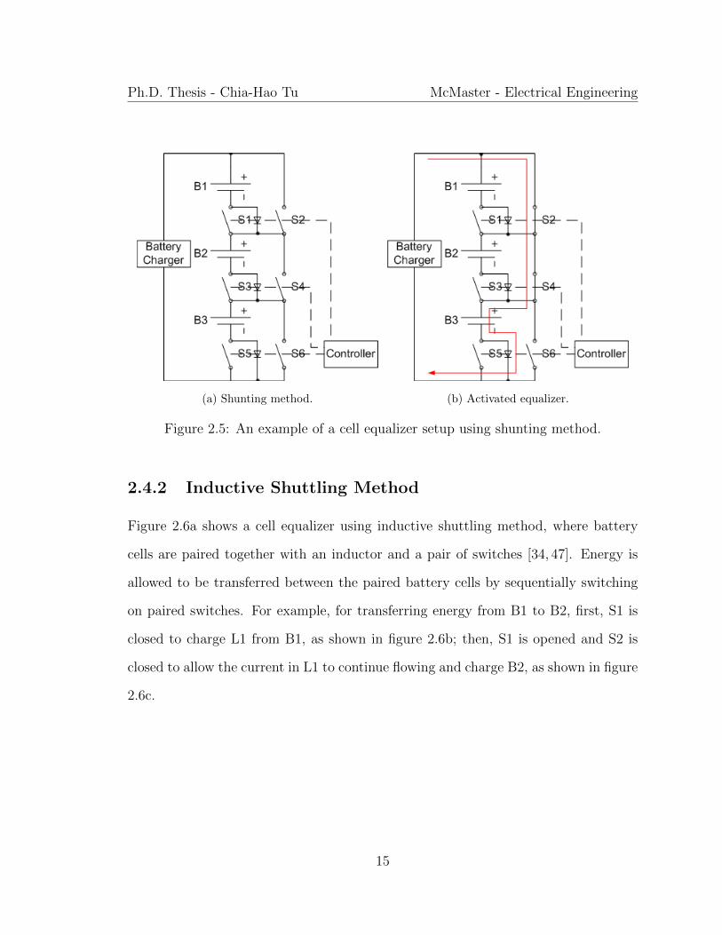
Figure 2.5a shows a cell equalizer using shunting method [61]. Switches and diodes
are used for re-routing the current; for example, figure 2.5b shows the switch con-
figuration, in which S2 and S4 are closed, allowing B3 to be charged by the battery
charger. By doing so, each battery cell can be fully charged one at a time. Shunting
method is very effective, however, the more battery cells there are, the slower the
balancing process is.
14
Ph.D. Thesis - Chia-Hao Tu McMaster - Electrical Engineering
(a) Shunting method. (b) Activated equalizer.
Figure 2.5: An example of a cell equalizer setup using shunting method.
2.4.2 Inductive Shuttling Method
Figure 2.6a shows a cell equalizer using inductive shuttling method, where battery
cells are paired together with an inductor and a pair of switches [34, 47]. Energy is
allowed to be transferred between the paired battery cells by sequentially switching
on paired switches. For example, for transferring energy from B1 to B2, first, S1 is
closed to charge L1 from B1, as shown in figure 2.6b; then, S1 is opened and S2 is
closed to allow the current in L1 to continue flowing and charge B2, as shown in figure
2.6c.
15

Ph.D. Thesis - Chia-Hao Tu McMaster - Electrical Engineering
(a) Inductive shuttling.
(b) Switching period 1. (c) Switching period 2.
Figure 2.6: An example of a cell equalizer setup using inductive shuttling method.
The balancing circuit of inductive shuttling method can operate in discontinuous
mode, which is a highly efficient soft-switching mode, and can operate during both
charging and discharging operations of the ESS. Because it is efficient and can be
designed with high switching frequency to reduce the size of inductors, it is suitable
for high power applications. However, the disadvantages are that it requires precision
16

Ph.D. Thesis - Chia-Hao Tu McMaster - Electrical Engineering
sensors and intelligent controllers to achieve soft-switching; these factors contribute
to the cost and complexities of the system which are not favorable for lower power
applications.
2.4.3 Capacitive Shuttling Method 1
Figure 2.7a shows a cell equalizer using capacitive shuttling method [27,31,57]. The
switches are controlled at the same time from one position to another allowing energy
to be transferred in between the neighboring cells. For example, if B2 is more charged
than B1, then during one switching period, B2 charges C1 as shown in figure 2.7b.
Then, during the next switching period, C1 gets connected to B1, so the current flows
from C1 to B1 as shown in figure 2.7c.
17

Ph.D. Thesis - Chia-Hao Tu McMaster - Electrical Engineering
(a) Capacitive shuttling v1.
(b) Switching period 1. (c) Switching period 2.
Figure 2.7: An example of a cell equalizer setup using capacitive shuttling method 1.
Comparing to the inductive shuttling method, the advantages of capacitive shut-
tling method 1 are that it is sensor-less, can operate during charging and discharging
operations of the ESS, and uses simple controllers to switch the capacitors. However,
the balancing power of the capacitive shuttling method 1 is relatively lower.
18

Ph.D. Thesis - Chia-Hao Tu McMaster - Electrical Engineering
2.4.4 Capacitive Shuttling Method 2
Figure 2.8a shows another variation of capacitive shuttling method [27, 31]. In this
case, a switch network is used to connect the battery cells to one capacitor instead of
having one capacitor per neighboring cells in the previous version. For example, for
transferring energy from B1 to B3, first, S1 and S2 are closed to connect B1 to C as
shown in figure 2.8b; then, S1 and S2 are opened, S5 and S6 are closed to connect C
to B3 for transferring the energy as shown in figure 2.8c.
(a) Capacitive shuttling v2.
(b) Switching period 1. (c) Switching period 2.
Figure 2.8: An example of a cell equalizer setup using capacitive shuttling method 2.
19

Ph.D. Thesis - Chia-Hao Tu McMaster - Electrical Engineering
Comparing to capacitive shuttling method 1, capacitive shuttling method 2 is
more efficient for a long string of ESS due to having the ability to select and tar-
get individual cells for balancing. However, because a single capacitor is used for
transferring energy, only two cells can be equalized at a time; thus, the capacitive
shuttling method 2 can be slower than capacitive shuttling method 1 in terms of
balancing speed. Furthermore, more sensors and intelligent controllers are required
in this method to target specific cells for balancing and control the switch network,
which would increase the design cost and complexities.
2.4.5 Pack-to-cell Method with Flyback Converter
Figure 2.9a shows a cell equalizer using a flyback converter for balancing the cells
[11,34]. In this setup, one flyback DC-DC converter is used with its output connected
to a switch network that can select a weaker battery cell to be charged, and input
connected to the entire battery string, hence, it is called a pack-to-cell method; if
the input and output connections are switched places, then the method becomes a
cell-to-pack one. The operation of this setup is as following. For example, when B2
is selected to be charged, first, S2, S3, S5, and S6 are switched so that the output of
the converter is connected to it, then S7 is switched on during the first part of the
switching period; S7, then, is switched off during the second part of the switching
period so that the converter transfer the energy into B2.
20

Ph.D. Thesis - Chia-Hao Tu McMaster - Electrical Engineering
(a) Method with flyback converter.
(b) Switching period 1. (c) Switching period 2.
Figure 2.9: An example of a cell equalizer setup using a flyback converter.
This pack-to-cell balancing method has the advantages of being able to operate
during both charging and discharging of the ESS, being applicable to both low and
high power applications, and having higher balancing efficiency. However, it requires
intelligent controllers to control the switch network and the power electronic converter
21

Ph.D. Thesis - Chia-Hao Tu McMaster - Electrical Engineering
that increase the design cost.
2.4.6 Pack-to-cell Method with Ramp Converter
Figure 2.10a shows a cell equalizer using pack-to-cell method with a ramp converter
[21,72]. For this setup, the even number and odd number of battery cells are charged
in different periods of time; a converter shown on the left side of figure 2.10a is
connected to an input that induces positive and negative current ramps. Thus, for
example, in the first part of switching period, a positive ramp current is induced, and
the energy is then transferred to B1 and B3 as shown in figure 2.10b. Then, in the
second part of switching period, a negative ramp current is induced, and then energy
is transferred to B2 as shown in figure 2.10c.
22

Ph.D. Thesis - Chia-Hao Tu McMaster - Electrical Engineering
(a) Method with ramp converter.
(b) Switching period 1. (c) Switching period 2.
Figure 2.10: An example of a cell equalizer setup using a ramp converter.
This pack-to-cell method using a ramp converter uses soft-switching technique
making the balancing very efficient compare to other methods that use traditional
power electronic converters such as flyback converters. However, the trade-offs are
that it requires a costly single-core multi-winding transformer with symmetrical wind-
ings and controllers to govern soft-switching of the converter.
23

Ph.D. Thesis - Chia-Hao Tu McMaster - Electrical Engineering
2.5 Summary
Advanced energy storage cells such as lithium-ion types of battery and UC require
advanced electronics to complement them for ensuring safe operations and quality
of performance. In this chapter, the fundamental of energy storage management
systems, cell equalization methods, and various examples of cell equalizers were pre-
sented and discussed. There are many variants of the management systems and cell
equalization methods. Some excel in high performance, and some excel in simplicity
and low cost that can be fitted into different suitable applications. This chapter fo-
cuses on battery management systems and equalizations because they are the most
popular choice as the main energy source amongst the others and are more intolerant
to fail states. However, such systems and methods can also be applied to UCs and any
other types of energy cells that are in need of complementary electronics. The next
chapter presents and discuss techniques and systems with emphasis on hybrid energy
storage system, which involve utilizing high performance power electronics, that have
the potential to improve performance and even reduce the number of series-connected
energy cells required for meeting load requirements and complementing the energy
management systems.
24
Chapter 3
Fundamentals of Hybrid Energy
Storage Systems
3.1 Introduction
In the previous chapter, the issues that come with more advanced ESS, their manage-
ment systems, and complementary electronics were presented and discussed. There
are ways, from a higher system level point-of-view, to assist and further improve the
performance and decrease the scale of ESSs capabilities and their management sys-
tems through the usage of PECs and combining multiple ESSs to form a HESS to
better regulate power flow and reduce the number of cells connected in series.
Reference [36] and [73] are two examples of utilizing a type of PEC, namely, a
current-fed double inductor push-pull dc-dc converter [1, 2, 13, 35, 48], to eliminate
the need of connecting battery cells in series to create high voltage to satisfy the
load requirement. In reference [36], the authors presented a design that couples
the aforementioned PEC with individual battery cell to form an individual energy
25

Ph.D. Thesis - Chia-Hao Tu McMaster - Electrical Engineering
module; then, the secondary winding of each energy module is connected in series
to form a final output for producing a much higher voltage level without having the
need to connect the battery cells in series. On the other hand, in reference [73],
the authors proposed a design that directly uses the aforementioned PEC to boost a
single battery cell voltage to a desirable output voltage level, hence eliminating the
need for a series-connected battery string that involves connecting large number of
battery cells in series and designing complicated battery management systems.
In this research study, there is interest in the option of using HESS techniques
to better an energy storage system. Many HESS configurations and their topologies
have been extensively studied. In the following sections, five fundamental HESS
configurations are presented and discussed.
3.2 Power Flow Efficiency and UC Energy Utiliza-
tion of HESS Configurations
The power flow efficiency and maximum UC energy utilization are the parameters
used here to compare the HESS configurations that are described later on in the
chapter. The maximum UC energy utilization is shown in equation (3.1) where Vmin
and Vmax are the minimum and maximum voltage allowed for the UC, respectively.
EUmax = 1 − Vmin2
Vmax2 (3.1)
Thus, using the aforementioned definition for UC energy utilization, Table 3.1
is created to illustrate five types of energy storage and their approximate voltage
ratio, Vmin
Vmax. Lithium polymer battery and UC have lower voltage ratio or, in other
26

Ph.D. Thesis - Chia-Hao Tu McMaster - Electrical Engineering
words, larger range of voltage operation level which can be desirable in terms of UC
energy utilization in some configurations and modes where they are coupled directly
together. In addition, lithium polymer battery has a higher operating voltage level in
comparison to other types of battery, so it requires fewer battery cells to stack up the
battery string voltage. From a design point of view, the fewer the series-connected
battery cells are, the fewer and less complicated the safety components and system are.
Therefore, for the purpose of comparison amongst the different HESS configurations,
lithium polymer battery and UC are used.
Table 3.1: Energy Storage Devices, Operating Voltage Range, and Voltage Ratio.
Energy Storage Device Operating Voltage Range Voltage Ratio
Lead Acid 1.7V - 2.1V 0.81
Nickel Metal Hydride 0.9V - 1.2V 0.75
Lithium Iron Phosphate 2.8V - 3.6V 0.78
Lithium Polymer 2.8V - 4.2V 0.67
UC 0V - 2.5V 0
3.3 Direct Parallel Connected Configuration
Figure 3.1 shows a HESS configuration wherein ESS1 and ESS2 are coupled together
either directly or through a simple passive component or switch, such as an inductor,
a resistor or diode. It appears to be a simple setup; however, one disadvantage is that
the system lacks control and regulation over the DC link voltage and ESS power flow.
27

Ph.D. Thesis - Chia-Hao Tu McMaster - Electrical Engineering
Because the two ESSs are coupled together directly, their voltage levels are locked
together; if a UC and a battery bank are used for this setup, then the UC energy
is not utilized as much as possible due to the fact that the battery voltage variation
range is much smaller than that of UC. Moreover, because of a lack of control and
regulation due to the simplicity of the system, extra efforts in design considerations
have to be made to ensure safe operations; for example, extra protection circuits
and/or over-sized ESSs might be needed to compensate the lack of voltage control
and power flow regulation.
Figure 3.1: Direct parallel connected HESS configuration.
Figure 3.2 shows the battery and UC HESS with a direct parallel connected con-
figuration that is present in figure 3.1.
Figure 3.2: Battery and UC HESS with direct parallel connected configuration.
There can be a component, either a passive component or a switch, that couples
the UC and the battery together; so the power loss in that component is considered,
and the efficiency is defined as ηComp. Therefore, the power flow efficiency of a battery
and UC HESS using this configuration is as shown in equation (3.2).
PLoad
PSource
=ηCompηBattPBatt + ηUCPUC
PBatt + PUC
(3.2)
28

Ph.D. Thesis - Chia-Hao Tu McMaster - Electrical Engineering
Since the battery and UC are directly coupled together, their voltage levels are
locked where in VBatt,min ≤ VUC ≤ VBatt,max. Thus, the amount of UC energy uti-
lization, using equation (3.3), is approximated to be 0.55 or 55%. UC’s voltage level
indicates the presence of a steady-state condition when it is equal to the battery volt-
age. Such configuration’s performance does reduce battery current to a degree due
to the UC’s capability to respond to transient current faster [23].
EUmax = 1 − VBatt,min2
VBatt,max2 = 1 − 0.672 = 0.55 (3.3)
In reference [39], a small bidirectional power electronic converter is integrated
with the electric machine’s internal inductors as shown in figure 3.3. However, the
trade-off is that the proposed topology requires a variable voltage input motor drive,
and also certain operations could only be done during low speed or standstill modes.
Figure 3.3: Example HESS topology [39].
Another example topology using direct parallel connected configuration can be
seen in figure 3.4 [46]. In this case, the authors propose coupling the battery and the
UC with a power diode. Because the application is a high-performance light-weight
29

Ph.D. Thesis - Chia-Hao Tu McMaster - Electrical Engineering
racing car (its powertrain is shown in figure 3.5), the power transients are highly
dynamic. The strategy is to use the UC for capturing all the regenerative energy and
use the diode for preventing any power to go into the battery; in other word, the
battery is only used for propulsion.
Figure 3.4: Example HESS topology [46].
Figure 3.5: Powertrain topology used in [46].
More example studies on passive, direct parallel connected configuration can be
found in references of [40, 84]. In the following sections, four active HESS configura-
tions are introduced; unlike the first configuration that uses passive components to
couple the ESSs together, they utilize power electronic converters.
30

Ph.D. Thesis - Chia-Hao Tu McMaster - Electrical Engineering
3.4 Cascaded Configuration Using One Power Elec-
tronic Converter
Active coupling methods using cascaded configuration with one PEC are more pop-
ular, and can be categorized as battery facing load (BFL) and UC facing load
(UCFL) [22, 23]. A topology that is BFL has an advantage of maintaining a more
stable DC link voltage than one that is UCFL. The reason is that a battery has a
lower voltage variation than UC. On the other hand, the purpose of having a UC is to
capture high transient power flow; topologies that are BFL have to use higher power
PECs that are designed to handle the UC’s power capability and the high transient
power required by the load. On the other hand, topologies that are UCFL require
smaller PECs to handle battery’s power capabilities [37].
Figure 3.6: Cascaded HESS configuration with one PEC.
Figure 3.6 shows a HESS configuration wherein ESS1 and ESS2 are coupled
through a PEC. Compared to the previous configuration where the ESSs are con-
nected directly, having a PEC in the configuration offers voltage control and power
flow regulation over the ESSs with a trade-off of lower power flow efficiency due to an
extra PEC stage. ESS1 in this configuration can be one of those more sensitive ESSs
such as a li-ion type of batteries that require protections and regulations. While,
on the other hand, ESS2 can be a UC that is capable of absorbing/delivering high
31

Ph.D. Thesis - Chia-Hao Tu McMaster - Electrical Engineering
transient power from/to the load. Moreover, in this HESS configuration, the UC is
allowed to discharge further; in other words, the UC’s energy is more utilized than
the previously mentioned directly connected HESS configuration.
Figure 3.7 shows two versions of the battery and UC HESS with a cascaded
configuration using one PEC; one version, figure 3.7a, shows the UC being connected
directly to the load (UCFL), and another version, figure 3.7b, shows the battery being
connected directly to the load (BFL).
(a) UC facing the load.
(b) Battery facing the load.
Figure 3.7: Battery and UC HESS with cascaded connected configuration with onePEC.
In this configuration, a PEC is used to couple the two ESSs, so the power flow
efficiency of each of the HESS version is shown in equation (3.4), for UCFL, and in
equation (3.5), for BFL.
PLoad
PSource
=ηPECηBattPBatt + ηUCPUC
PBatt + PUC
(3.4)
PLoad
PSource
=ηBattPBatt + ηPECηUCPUC
PBatt + PUC
(3.5)
Because the battery and the UC are coupled together using a PEC, the UC’s
voltage variation can be more flexible and not be confined by the battery operation
32

Ph.D. Thesis - Chia-Hao Tu McMaster - Electrical Engineering
voltage range. Typically the UC then is allowed to discharge up to half of its maximum
voltage level [9]. Thus, for both versions of the HESS using this cascaded connected
configuration, the UC energy utilization, using equation (3.6), is typically 0.75 or
75%.
EUmax = 1 − VUC,min2
VUC,max2 = 1 − 0.52 = 0.75 (3.6)
Figure 3.8, from reference [9], shows an example HESS topology of combined
cascaded configuration using one PEC and direct parallel connected configuration.
The UC is directly connected to the DC bus, and the battery and UC are connected
through a bi-directional buck-boost converter that is rated at the battery’s power
level. In addition, a power diode is added to form another power path in between
the battery and the UC; this provides an additional low-power and high efficient
operation mode where the battery can provide power directly through the diode to
the load and the UC.
Figure 3.8: Example HESS topology [9].
Reference [38] presents special topologies of HESS integrated with the motor in-
verter based on the idea of avoiding using DC-DC converter as much as possible to
reduce power losses. Different topologies are introduced in the reference; for example,
in one topology, the UC is used to accelerate the vehicle up to a certain speed, then
33

Ph.D. Thesis - Chia-Hao Tu McMaster - Electrical Engineering
the HESS switches to the battery for constant speed cruising. In another topology, a
small bidirectional PEC is used to link the battery bank to the UC bank as shown in
figure 3.9.
Figure 3.9: Example HESS topology [38].
Another example topology can be found in references [22,23], shown in figure 3.10.
The battery and UC are coupled at the cell level via individual buck-boost converters
to integrate together the multi-input/output PEC and the active balancing circuits
of both UC and battery cells.
34

Ph.D. Thesis - Chia-Hao Tu McMaster - Electrical Engineering
Figure 3.10: Example HESS topology [22,23].
3.5 Cascaded Configuration Using Two Power Elec-
tronics Converters
Figure 3.11 shows a HESS configuration wherein ESS1 and ESS2 are coupled through
a PEC, and, in addition to that, another PEC is used to couple the load with ESS2.
This configuration has full voltage and power flow controls over the DC link and
the two ESSs. However, since the ESSs and the PECs are connected in a cascaded
fashion, the total efficiency is the multiplication of the individual ESS’s and PEC’s
efficiency. Also, the subsequent PEC that is closer to the load is required to handle
35

Ph.D. Thesis - Chia-Hao Tu McMaster - Electrical Engineering
the power provided by both ESSs combined. As a result, the size and cost of the
whole system of this cascaded configuration are relatively larger than the previous
configuration wherein fewer PEC is used.
Figure 3.11: Cascaded HESS configuration with two PECs.
Similar to the cascaded connected configuration with one PEC, there can be two
versions of this configuration for a battery and UC HESS. Figure 3.12a shows one
version with the UC closer to the load (UCFL); on the other hand, figure 3.12b shows
another version with the battery closer to the load (BFL).
(a) UC closer to the load.
(b) Battery closer to the load.
Figure 3.12: Battery and UC HESS with cascaded connected configuration using twoPECs.
The power flow efficiency expressions of this battery and UC HESS are shown in
equation (3.7), for UCFL, and (3.8), for BFL. As can be seen in the expressions, in
comparison to the previous case of HESS configuration with one PEC, an additional
36

Ph.D. Thesis - Chia-Hao Tu McMaster - Electrical Engineering
power efficiency factor of PEC2 is present, hence, decreases the entire system effi-
ciency. Although the additional PEC brings more power losses to the overall HESS
system, it can be beneficial to have the ability to maintain a fixed and stable load
voltage. For example, if such HESS system is used with a traditional buck-mode
motor inverter, then the fixed output voltage from the HESS system can help the
motor inverter to operate within its optimal operating range and control strategy.
PLoad
PSource
=ηPEC2(ηPEC1ηBattPBatt + ηUCPUC)
PBatt + PUC
(3.7)
PLoad
PSource
=ηPEC2(ηBattPBatt + ηPEC1ηUCPUC)
PBatt + PUC
(3.8)
Similarly to the previous case where the HESS uses one PEC for coupling the
battery and the UC, in this case where the HESS utilizes two PECs, the UC is
allowed to discharge to at least half of its maximum voltage because its voltage level
is not restricted by the battery. Thus, the UC energy utilization, using equation (3.9),
is at least 0.75 or 75% for both versions.
EUmax = 1 − VUC,min2
VUC,max2 = 1 − 0.52 = 0.75 (3.9)
One example topology using the HESS configuration with two PECs (UCFL) can
be found in reference [53], wherein the battery is being connected to a boost converter,
then its output is connected to a UC which is then connected to a bi-directional buck-
boost converter, shown in figure 3.13.
37

Ph.D. Thesis - Chia-Hao Tu McMaster - Electrical Engineering
Figure 3.13: Example HESS topology [53].
3.6 Parallel-Connected Output Configuration
Figure 3.14 shows a HESS configuration wherein ESS1 and ESS2 are not coupled in
the cascaded fashion; instead, each ESS is connected to a dedicated PEC, and the
outputs of the PECs are then connected in parallel together with the load. By doing
so, the total efficiency, cost, and size of the PECs are better than the cascaded HESS
configuration with two PECs while maintaining the feature of having full control and
regulation over the ESSs and output voltage level.
Figure 3.14: Parallel-connected output HESS configuration.
Figure 3.15 shows the battery and UC HESS using parallel-connected output
configuration.
38

Ph.D. Thesis - Chia-Hao Tu McMaster - Electrical Engineering
Figure 3.15: Battery and UC HESS with parallel-connected output configuration.
The power flow efficiency for such setup is given by equation (3.10).
PLoad
PSource
=ηPEC1ηBattPBatt + ηPEC2ηUCPUC
PBatt + PUC
(3.10)
Because the battery and UC are not connected directly, the UC can be allowed to
discharge to up to half of its maximum voltage level, typically. Thus, the UC energy
utilization, using the equation (3.11), is 0.75 or 75%.
EUmax = 1 − VUC,min2
VUC,max2 = 1 − 0.52 = 0.75 (3.11)
One example topology using this parallel-connected output configuration can be
found in references [15, 67]; the topology that is presented couples battery, UC, and
fuel cell together using buck-boost converters, as shown in figure 3.16.
39

Ph.D. Thesis - Chia-Hao Tu McMaster - Electrical Engineering
Figure 3.16: Example HESS topology [15].
3.7 Active Coupling Configuration Using a Multi-
input Power Electronics Converter
Figure 3.17 shows an HESS configuration similar to the parallel-connected output
configuration. In this case, the two PECs are integrated together as one PEC to
reduce the component count. By doing so, the cost and size can be further reduced.
40

Ph.D. Thesis - Chia-Hao Tu McMaster - Electrical Engineering
Figure 3.17: HESS configuration with a multi-input PEC.
Figure 3.18 shows the battery and UC HESS with an active coupling configuration
using a multi-input PEC.
Figure 3.18: Battery and UC HESS with active coupling configuration using a multi-input PEC.
In this case, though the two PECs are integrated together, they can still be con-
sidered two separate PECs with two separate power flow efficiency from the general
system level point-of-view; the benefits of integration can only be quantified by ap-
plying it to specific topology and application. As a result, the power flow efficiency
and energy utilization are the same, and can potentially be better, as the HESS that
uses a parallel-connected output configuration, which are shown in equations (3.10)
and (3.11).
One example of a HESS topology using the said active coupling with multi-input
41

Ph.D. Thesis - Chia-Hao Tu McMaster - Electrical Engineering
PEC configuration can be found in reference [54], shown in figure 3.19, wherein the
authors propose a topology that couples the battery and the UC using an integrated
PEC that combines the inductors of the two buck-boost converters into one.
Figure 3.19: Example HESS topology [54].
3.8 Summary
HESS is a concept for combining different types of ESS together and utilizing the
specialized strengths of each individual ESS in order to improve the overall perfor-
mance of power supply systems in terms of power capability, energy capacity, and
energy management. Moreover, HESS not only improves the performance of the
overall storage system, but also help reduces the size of the ESSs resulting in simpli-
fying their management systems to create a more effective system. In this chapter,
five fundamental HESS configurations that have been extensively studied by other re-
searchers were introduced. Also, several battery and UC HESS topologies that have
been proposed by other researchers were presented. Coupled with what was discussed
in chapter 2, this chapter on the fundamentals of HESS served as the foundation and
inspiration to craft the concept and theory of the SPR-HESS configuration, which is
the research interest and is presented in the next chapter.
42

Chapter 4
Series-Parallel Reconfigurable
Hybrid Energy Storage Systems
4.1 Introduction
In the previous chapter, the fundamental HESS configurations were introduced and
discussed. A passive HESS configuration, that couples ESSs directly together through
at most a simple component, has an advantage of having higher system efficiency due
to having no power transfer loss. However, such passive configuration, although
appears to be simple, lacks any control over the voltage and power flow of the ESSs
and the output of the HESS system; therefore, the ESSs often need to be over-sized so
that their power capability match not only the load requirement but also one another’s
or be complemented with extra safety systems to avoid over-current discharging or
charging and ensure safe operation. On the other hand, an active HESS configuration,
that utilizes PECs to couple ESSs together, has the advantage of having control over
the voltage and power flow of the system and the ESSs with a trade-off of having
43

Ph.D. Thesis - Chia-Hao Tu McMaster - Electrical Engineering
lower power transfer efficiency than a passive HESS configuration.
In this chapter, the theory of a new kind of HESS configuration using series-
parallel reconfiguration (SPR) technique that inherits the advantages of both passive
and active HESS configurations will be presented and discussed.
4.2 Series-Parallel Shifting of Energy Storage Sys-
tems
Several concepts and topologies of series-parallel shifting of an ESS, mainly a capacitor
bank, have been proposed previously. For example, in [23], the authors proposed a
new HESS topology with a parallel-series shifting UC bank in which the battery
and UC bank are coupled directly through a switch. In reference [9], the authors
presented a concept and implementation of electronic gears with a series-parallel
shifting battery bank and a series-parallel shifting axial fluxed brushless DC motor
using electromechanical switches to improve power propulsion efficiency and extend
the constant power region of the motor.
References [18, 70, 75] presented a reconfigurable UC bank. Reference [70] pre-
sented the concept of series-parallel shifting of a capacitor bank using two different
types of changeover circuits shown in figures 4.1a and 4.1b; the switches used in
experimental setup are thyristors. They showed that using changeover circuits the
overall electrical path efficiency can be higher than when using traditional PECs.
References [18, 75] presented a similar topology as [70] with a different focus on the
effect of using different capacitances so that the overall capacitance of the UC bank
changes after shifting. The major advantage of unbalanced shift UC variant over the
44

Ph.D. Thesis - Chia-Hao Tu McMaster - Electrical Engineering
balanced one is having lower output voltage ripple. However, the challenge is to ini-
tially charge up the UC cells due to having different cell capacitance. Reference [81]
presented battery parallel-series shifting alongside with a parallel-series shifting axial
fluxed BLDC motor using electromechanical switches to improve power propulsion
efficiency and extend the constant power region of the machine. The experiment was
done on a scooter later on in [80]. In reference [80], parallel-series shifting of the
battery bank was eliminated; instead, a UC bank was introduced and it was directly
paralleled with a battery bank via a semiconductor device. In reference [71], the
author proposed a new HESS topology with a parallel-series shifting UC bank; the
battery and UC banks are coupled directly through a switch as shown in figure 4.2.
(a) Type 1 (b) Type 2
Figure 4.1: Capacitor changeover circuits
45

Ph.D. Thesis - Chia-Hao Tu McMaster - Electrical Engineering
Figure 4.2: HESS topology with changeover circuit for UC.
4.3 Introduction to a Hybrid Energy Storage Sys-
tem Utilizing Series-Parallel Reconfiguration
Technique
The theory and major design considerations have to be first developed before design-
ing and implementing a practical topology for the SPR-HESS configuration. Because
a battery bank is used, it is recommended to use a PEC to protect and regulate the
power flow of the battery bank. On the other hand, a UC bank has relatively much
higher peak power than that of a battery bank, so if another PEC is used for the
UC bank, the PEC has to be sized to handle the peak power capability from the UC
bank, which is expected to be much larger than that of a battery bank. Moreover,
cascading two power electronic converters results in lower overall system efficiency
for power and energy conversion aforementioned in the introduction section. Thus,
46

Ph.D. Thesis - Chia-Hao Tu McMaster - Electrical Engineering
it is recommended to have the UC bank directly connected to the DC link (UCFL)
so that the power can be directly transferred between the load and the UC bank
much like the parallel configuration shown in figure 3.1 and 3.6 with ESS2 as the UC
bank. However, the option of having battery directly connected to the load (BFL)
is also a viable option that provides a more stable output voltage for the load with
a trade-off of having a larger PEC to handle the UC’s higher power capability; the
choice between the two variants depends on the application and design constraints.
In this chapter, there is more interest in presenting the theory of the SPR-HESS and
its functionalities.
There are two general issues that come with all the other active HESS configu-
rations, SPR-HESS included. First, the UC bank’s voltage level changes greatly as
it charges or discharges, compared to that of a battery bank. Second, in electrified
vehicles, a traditional motor controller has a minimum voltage operation requirement;
this limits how much the UC bank can discharge its energy to the load for the UCFL
variant. The first issue can be overcome by properly sizing the UC bank so that its
operating voltage is within the motor controller’s and PEC’s operation range. To
overcome the second issue, one can design a special motor controller or implement
series-parallel shifting technique to further utilize the UC bank’s energy while boost-
ing the output voltage to a proper level for the motor controller to operate; in this
case, the latter option is used. To fully utilize the UC bank’s energy, the UC voltage
has to reach zero; such percent energy utilization is realized in equation (4.1), wherein
V1 and V2 are the initial and final UC voltage, respectively. This can be theoretically
done through connecting the UC in series with a battery bank allowing the UC to
be completely discharged while having the battery bank to maintain a proper voltage
47

Ph.D. Thesis - Chia-Hao Tu McMaster - Electrical Engineering
level for the motor controller to operate; for practical and safety reasons, the UC
bank should never be completely discharged. This proposed HESS has the ability to
electrically connect multiple ESSs in series, parallel, or series-parallel configuration;
hence it is called a series-parallel reconfigurable HESS or SPR-HESS.
∆E
E1
=12C(VUC,max
2 − VUC,min2)
12CVUC,max
2 =(VUC,max
2 − VUC,min2)
VUC,max2 = 1 − VUC,min
2
VUC,max2 (4.1)
Figure 4.3 shows two different general configurations of the proposed HESS. Figure
4.3a shows a simple SPR-HESS. Although the direct connection of the UC and battery
banks is a simple solution, there is no voltage and power regulation over the DC link
much like the passive HESS configuration shown in figure 3.1. On the other hand,
when a power electronic converter is incorporated into the HESS, as shown in figure
4.3b, the configuration that is much like the traditional HESS configuration shown
in figure 3.17, the power electronic converter allows the transfer of power and energy
from one ESS to another; this provides another layer of control over the DC link. The
PEC can regulate the transfer of power and energy from one ESS to another. There
is interest in the form shown in figure 4.3b.
(a) Form 1. (b) Form 2.
Figure 4.3: SPR-HESS general forms.
48

Ph.D. Thesis - Chia-Hao Tu McMaster - Electrical Engineering
4.4 Theoretical System Level Operation Modes
Figure 4.4 shows five distinct system level operation modes, M1 through M5, that are
defined for the SPR-HESS with UCFL. Depending on the applications, having BFL
is also an option just like other active HESS configurations. However, there is more
interest in the form with UCFL, and its system level operation modes are described
here; the concept can be directly applied to the form of BFL.
4.4.1 Mode 1
Figure 4.4a shows the system level operation mode one, M1, wherein the battery and
the UC are coupled through the power electronic converter (PEC). Notice that in
this mode, the figure does not show the DC link of the system; this mode may occur
when, for example, the electrified vehicle stops at a traffic light or is in a standstill.
During this mode, the power flow can be bi-directional; the battery can recharge the
UC or vice versa via the PEC.
4.4.2 Mode 2
Figure 4.4b shows the system level operation mode two, M2, wherein the UC connects
to the DC link directly. In this mode, the battery and PEC are decoupled from the
system, and the UC acts as the primary power source or sink for the system. This
mode may occur when the battery is overcharged or undercharged and needs to be
disconnected from the system; or this mode may also occur when the UC alone is
enough for providing/taking power to/from the load, for example, when the vehicle
has short pockets of duty cycle that it starts and stops frequently being driven in a
49

Ph.D. Thesis - Chia-Hao Tu McMaster - Electrical Engineering
city.
4.4.3 Mode 3
Figure 4.4c shows the system level operation mode three, M3, wherein the battery is
coupled to the DC link via the PEC, and the UC is disconnected from the system.
In this mode, the power flow can also be bi-directional, and may occur when lower
power is required from the load. Compared with the system in mode 2, the system
in mode 3 has a lower peak power capability in either direction of the power flow.
4.4.4 Mode 4
Figure 4.4d shows the system level operation mode four, M4, which is similar to M1
except that in this case the DC link is connected to the SPR-HESS. Compared with
M1, M2, and M3, mode four has a higher power capability in either direction of the
power flow.
4.4.5 Mode 5
The previously described four modes, M1 through M4, are all considered as paral-
lel modes. Figure 4.4e shows the system level operation mode five, M5, and it is
considered as a series and series-parallel mode. In this operation mode, the UC and
battery are coupled to form a series connection with the DC link; also, through the
PEC, power transfer may occur between the battery and the UC that has a form of
a parallel connection. Because in this mode SPR-HESS has both series and parallel
connections, M5 is considered as a series and series-parallel mode.
50

Ph.D. Thesis - Chia-Hao Tu McMaster - Electrical Engineering
(a) M1 (b) M2 (c) M3
(d) M4 (e) M5
Figure 4.4: System level operation modes (UCFL).
4.5 Power Flow Efficiency and UC Energy Uti-
lization of HESS Configuration Using Series-
Parallel Reconfigurable Technique
Figure 4.5 shows the two variations as well as their equivalent parallel and series mode
forms of a battery and UC HESS configuration using series-parallel reconfigurable
technique; in variation form 1 (UCFL), 4.5a, the PEC is able to have complete control
over the power flow, in and out of the battery during parallel mode as opposed to
variation form 2 (BFL), 4.5b. When the HESS is in parallel mode, the equivalent
HESS configuration of each variation is shown in figure 4.5c for form 1 and in figure
4.5d for form 2. When the HESS is in series mode, the equivalent HESS configuration
of each variation is the same and is shown in figure 4.5e.
51

Ph.D. Thesis - Chia-Hao Tu McMaster - Electrical Engineering
(a) Form 1. (b) Form 2.
(c) Form 1 - Parallel Mode. (d) Form 2 - Parallel Mode.
(e) Form 1 & 2 - Series Mode.
Figure 4.5: Battery and UC HESS with series-parallel reconfigurable configuration.
For this HESS configuration, during the parallel mode, the equivalent configura-
tions for the two forms resembles the cascaded HESS configuration that utilizes one
PEC. Thus, the power flow efficiency and the energy utilization are the same as the
cascaded HESS configuration that utilizes one PEC which are shown in equations
(3.4) for UCFL and (3.5) for BFL with UC energy utilization of 0.75 or 75%. For
convenience, those equations are repeated below:
PLoad
PSource
=ηBattPBatt + ηPECηUCPUC
PBatt + PUC
(4.2)
PLoad
PSource
=ηPECηBattPBatt + ηUCPUC
PBatt + PUC
(4.3)
52

Ph.D. Thesis - Chia-Hao Tu McMaster - Electrical Engineering
EUmax = 1 − VUC,min2
VUC,max2 = 1 − 0.52 = 0.75 (4.4)
On the other hand, during the series mode, the battery and UC are coupled in
series and connected to the load directly. Thus, the power flow efficiency can be
represented by
PLoad
PSource
=ηBattPBatt + ηUCPUC
PBatt + PUC
(4.5)
Because the UC and the battery are connected in series, the UC is allowed to
discharge, in theory, completely. Therefore, the UC energy utilization, using equation
4.6, is 1.0 or 100%.
EUmax = 1 − 0
VUC,max2 = 1.0 (4.6)
4.6 Comparative Analysis
The comparative analysis is based on power flow efficiency and the maximum potential
UC energy utilization within reasonable operations that are not application based.
Table 4.1 shows the rankings of the power flow efficiency and UC energy utilization
of the HESS configurations from system level point-of-view based on the discussions
in chapter 3 and the previous sub-section.
53

Ph.D. Thesis - Chia-Hao Tu McMaster - Electrical Engineering
Table 4.1: Power Flow Efficiency and UC Energy Utilization Rankings.
HESS Power Flow UC Energy
Configuration Efficiency Ranking Utilization
Direct Parallel Connected 1 6
Cascaded With One PEC 3 2
Cascaded With Two PECs 6 2
Parallel Connected Output 4 2
Active Coupling With Multi-input PEC 4 2
SPR-HESS 2 1
The direct parallel connected configuration is ranked first at power flow efficiency
and ranked sixth at UC energy utilization; the coupling method is through either a
direct connection or a fundamental device such as a passive component or a switch;
so the major power losses are from the ESSs themselves which results in having the
highest system efficiency out of the six configurations. On the other hand, the UC
energy utilization is the worst out of the six configurations due to having the battery
and UC voltage level tied together, wherein the UC’s minimum operating voltage
level is limited by that of the battery.
Cascaded with one PEC configuration has the rankings of power flow efficiency
and UC energy utilization at third and second, respectively, amongst the six config-
urations. The power flow efficiency is ranked below the direct parallel connected and
SPR-HESS configurations due of having power losses at one PEC. However, the UC
54

Ph.D. Thesis - Chia-Hao Tu McMaster - Electrical Engineering
utilization is much higher than the direct parallel connected configuration where the
UC’s minimum operating voltage level is not limited by the battery.
Cascaded with two PECs configurations is ranked sixth at power flow efficiency
and ranked second at UC energy utilization. Because there are two stages of PECs,
the efficiencies multiply; as a result, the power flow efficiency is the worst out of the
six configurations. On the other hand, the UC energy utilization is ranked second
similarly to the cascaded with one PEC configuration where the UC’s voltage level is
not limited to the battery’s.
Parallel connected output and active coupling with multi-input PEC configura-
tions share the same rankings of power flow efficiency and UC energy utilization at
fourth and second, respectively, out of the six configurations due to having fundamen-
tally the same concept, except that one is a more integrated solution. The reason that
their power flow efficiency is ranked below the cascaded with one PEC configuration
is that two PECs are used; however, because the PECs are connected in parallel, the
power transferring is more efficient than the cascaded with two PECs configuration.
Similarly, with the same reasoning, the UC energy utilization is ranked second just
like the aforementioned configurations that utilize PECs.
Lastly, SPR-HESS configuration is ranked second in power flow efficiency and first
in UC utilization amongst the six configurations. Its power flow efficiency is less than
the direct parallel connected configuration due to having a PEC, but higher than the
other configurations because of the series operation mode where the ESSs are directly
connected to the load. The UC utilization of SPR-HESS configuration is the highest
because not only it has the advantage of non-restricted UC minimum voltage level
like other configurations with PECs, but also the UC can be fully discharged for full
55

Ph.D. Thesis - Chia-Hao Tu McMaster - Electrical Engineering
energy utilization during series mode.
4.7 Design Considerations and Limitations of SPR-
HESS
When using UC in SPR-HESS series mode, UC’s voltage level, in practical applica-
tions, should have a positive minimum operation limit that is non-zero as a safety
margin even though some UCs are able to operate in negative voltage polarity for a
short period of time. Application-specific properly sized ESSs are crucial to account
for system operation limits. For example, when using UC and battery for the SPR-
HESS, in series mode, where the battery and the UC are connected directly to the
load, the ESSs should be sized properly to not only meet the load requirements but
also have the safety margin to provide and absorb the load power under exceptional
situations.
In the case of UCFL, similar to the other configurations with UCFL variants,
the output voltage of the SPR-HESS varies. The load has to be capable of handling
variable voltage input due to the voltage operation range of the UC. References [7,9]
also have discussed and addressed the nature of voltage variation and its applica-
tions due to their UCFL HESS configuration. HESS configurations with UCFL are
applicable to the variable voltage inverters for optimizing the overall electric power-
train efficiency depending on the power load and speed; such technique can be found
in patent [24]. Moreover, Toyota’s commercialized HEVs also incorporate variable
voltage inverters in their electrified powertrains, which for example can have input
operation voltage ranges from 200V to 650V for Prius and 250V to 650V for Camry
56

Ph.D. Thesis - Chia-Hao Tu McMaster - Electrical Engineering
depending on the speed and power load [51,52].
On the other hand, similar to the other configurations with at least one PEC,
SPR-HESS is a flexible configuration and can also be configured in BFL so that the
output voltage, in parallel mode, is much more stable and more suitable for traditional
applications and loads. However, as discussed in previous sections, the PEC has to
be sized up to match the UC power capability which results in a larger PEC design
and higher power loss than that in the case of having UCFL.
Therefore, like designing for any other HESS configurations having their unique
setups and applications, one must know the aforementioned limitations and trade-offs,
and then consider them carefully when designing an application specific SPR-HESS.
4.8 Summary
In this chapter, the theory of the SPR-HESS configuration, as well as its operation
modes, are introduced and presented. Then, comparative analysis is discussed to
compare the SPR-HESS and all the other HESS configurations in terms of power
flow efficiency and energy utilization in the case of battery and UC type of HESS.
Lastly, design limitations and considerations are discussed. In the next chapter, an
example SPR-HESS topology, that is based on the theory and design considerations
discussed, is designed and studied using simulation tools.
57

Chapter 5
Simulation and Case Study of a
Series-Parallel Reconfigurable
Hybrid Energy Storage System
Topology
5.1 Introduction
In this chapter, a working topology is crafted to realize the SPR-HESS operation
theory and configuration concept mentioned in the previous chapter. In section 5.2,
detailed descriptions of an SPR-HESS topology with five major operating modes
and their corresponding sub-operating modes with switching tables are presented.
In section 5.3, power management and two proposed control strategies that can be
implemented with the proposed SPR-HESS topology are described. In section 5.4,
58

Ph.D. Thesis - Chia-Hao Tu McMaster - Electrical Engineering
PEC analytical models and feedback control transfer functions for three major modes:
buck, boost, and buck-boost are presented. Simulation setup is presented in section
5.5. Lastly in section 5.6, simulation results are presented and discussed.
5.2 Description of Topology Operation Modes
Figure 5.1 shows one of the conceptual implementations in the context of electrified
vehicle application of SPR-HESS with an additional ICE-GEN and its motor drive as
an additional ESS. This conceptual implementation is aimed to use in an electrified
vehicle and was first presented in our first publication [74].
Figure 5.1: Conceptual implementation 1.
The conceptual HESS topology shown in figure 5.1 consists of several bidirectional
switches and a bidirectional power electronics converter that connects the battery
bank to the UC bank and ICE-GEN. S1 and S2 can switch the DC link ground to
either UC bank ground or battery bank ground while S3 can connect/disconnect ICE-
GEN and the power electronic converter to/from the rest of the components. S1, S2
and S3 are bidirectional switches for switching in and out the ESSs. Because they are
not being switched continuously at high frequency, any type of switch configuration
59

Ph.D. Thesis - Chia-Hao Tu McMaster - Electrical Engineering
such as those shown in figure 5.2 that allow bidirectional current flow can be used.
(a) (b) (c)
Figure 5.2: Different types of bi-directional switches.
One major disadvantage of this version of conceptual HESS topology presented
is that, from a practical point-of-view, the UC, being directly coupled to the ICE-
GEN sets motor drive in some operation modes, should not be completely discharged
without using a special motor controller. The reason for this is that when the UC is
discharged completely, its voltage reaches zero hence shorting the motor drive that is
coupled to it. Without using a special motor controller, the ICE-GEN set has to be
shut down or disconnected until the UC regenerates back a certain amount of energy
to reach an acceptable voltage level for the ICE-GEN set to operate. That limits the
number of the operation modes and the flexibilities that the SPR-HESS potentially
offers. Thus, a more practical way of implementing SPR-HESS for an HEV or a
PHEV is to parallel-couple the ICE-GEN set with the battery or DC-link where the
voltage level is more stable; when this is the case, ICE-GEN set does not need to
be included to show the functionalities and concepts of the SPR-HESS as the case is
more related to the topics of hybrid vehicle powertrain architectures. More detailed
operation mode descriptions and simulation study case can be found in reference [74].
Thus, a better conceptual implementation for SPR-HESS is developed and shown
in figure 5.3 wherein the ICE-GEN set is removed and S3 is moved to the negative
terminal of the UC bank. With this conceptual implementation, the five system level
60

Ph.D. Thesis - Chia-Hao Tu McMaster - Electrical Engineering
operation modes aforementioned are realized; the following sub-sections describe the
implemented modes in details.
Figure 5.3: Conceptual implementation 2.
5.2.1 Mode 1
Figure 5.4a shows the topology level implementation of mode one where system-level
form was shown in figure 4.4a and described in Chapter 4. As mentioned in Chapter
4, the power flow is bi-directional; in general, in this mode S1 and S2 are turned off to
disconnect the SPR-HESS from the DC Link while S3 is turned on to couple the UC
and battery in series; as a result, the battery and UC are coupled in parallel through
a buck-boost-like converter. Because the power flow is bi-directional, there are two
distinctive sub-modes, M1-1, and M1-2, with two different sets of switching patterns.
For each sub-mode, there are two switching periods, a and b, shown in table 5.1. In
the case of sub-mode M1-1, the power is transferred from the battery to the UC bank;
first, during M1-1a, S4 is turned on to charged the inductor with the battery while
S5, D4, and D5 are off as shown in table 5.1 M1-1a and in figure 5.4b; then during
M1-1b, S4 is turned off while S5 and D4 remain off, and D5 is conducting, as shown
61

Ph.D. Thesis - Chia-Hao Tu McMaster - Electrical Engineering
in table 5.1 M1-1b and in figure 5.4c, to provide a continuous current path for the
inductor current and transfer the power to the UC. On the other hand, in the case of
sub-mode M1-2, the power is transferred from the UC to the battery bank. Similar to
sub-mode M1-1, first, during M1-2a, S5 is turned on to charged the inductor with the
UC while S4, D4, and D5 are off as shown in table 5.1 M1-2a and in figure 5.4d; then
during M1-2b, S5 is turned off while S4 and D5 remain off, and D4 is conducting, as
shown in table 5.1 M1-2b and in figure 5.4e, to provide a continuous current path for
the inductor current and transfer the power to the battery.
62

Ph.D. Thesis - Chia-Hao Tu McMaster - Electrical Engineering
(a) Topology implementation of
M1
(b) M1-1a (c) M1-1b
(d) M1-2a (e) M1-2b
Figure 5.4: Mode 1.
63

Ph.D. Thesis - Chia-Hao Tu McMaster - Electrical Engineering
Table 5.1: M1 switching table
S1 S2 S3 S4 S5 D4 D5
M1-1a 0 0 1 1 0 0 0
M1-1b 0 0 1 0 0 0 1
M1-2a 0 0 1 0 1 0 0
M1-2b 0 0 1 0 0 1 0
5.2.2 Mode 2
Figure 5.5a shows the topology level implementation of mode two shown in figure
4.4b wherein only the UC is coupled to the DC link directly in parallel. Table 5.2 and
figure 5.5b show the switching pattern for mode two, wherein S1, S4, S5, D4, and D5
are off, and S2 and S3 are on allowing bi-directional power transfer between the DC
link and the UC.
(a) Topology implementation of
M2
(b) M2 Power Flow
Figure 5.5: Mode 2.
64

Ph.D. Thesis - Chia-Hao Tu McMaster - Electrical Engineering
Table 5.2: M2 switching table
S1 S2 S3 S4 S5 D4 D5
M2 0 1 1 0 0 0 0
5.2.3 Mode 3
With the recommended conceptual implementation 2, mode 3 has two variations,
a and b, shown in figures 5.6a, and 5.8a, respectively, wherein variation a has four
sub-modes while variation b has two. In general, for both variations, the UC is
disconnected from the system completely.
For mode 3 variation a, S1 is turned on, and S2 and S3 are turned off in general
as shown in figure 5.6a; as a result, the battery and DC link are connected via the
PEC in boost, buck, or direct mode. There are two sub-modes, M3a-1 and M3a-2
for the different direction of the power transfer, and each sub-mode has 2 switching
periods, a and b.
65

Ph.D. Thesis - Chia-Hao Tu McMaster - Electrical Engineering
(a) Topology implementation of
M3 variation a
(b) M3a-1a (c) M3a-1b
(d) M3a-2a (e) M3a-2b
Figure 5.6: Mode 3 variation a - boost or buck modes.
66

Ph.D. Thesis - Chia-Hao Tu McMaster - Electrical Engineering
(a) M3a-3 (b) M3a-4
Figure 5.7: Mode 3 variation a - direct modes.
Table 5.3: M3 switching table - variation a
S1 S2 S3 S4 S5 D4 D5
M3a-1a 1 0 0 1 0 0 0
M3a-1b 1 0 0 0 0 0 1
M3a-2a 1 0 0 0 1 0 0
M3a-2b 1 0 0 0 0 1 0
M3a-3 1 0 0 0 0 0 1
M3a-4 1 0 0 0 1 0 0
For the first sub-mode, M3a-1, the battery is providing power to the DC link via
the PEC in boost mode. During the first switching period, S4 is turned on allowing
the battery to charge the inductor while S5, D4, and D5 are off, as shown in table 5.3
M3a-1a and in figure 5.6b. Then, during the second switching period, S4 is turned
67

Ph.D. Thesis - Chia-Hao Tu McMaster - Electrical Engineering
off, S5 and D4 remain off, and D5 is conducting, as shown in 5.3 M3a-1b and in figure
5.6c, to provide a current path for the inductor to transfer the stored energy to the
DC link.
For the second sub-mode, M3a-2, the DC link is providing power to the battery
via the PEC in buck mode. During the first switching period, S5 is turned on allowing
the current to flow from the DC link to the battery through the inductor; during this
period, S4, D4, and D5 are off, as shown in table 5.3 M3a-2a and in figure 5.6d. Then,
during the second switching period, S5 is turned off, S4 and D5 remain off, and D4
is conducting acting as a freewheeling diode for the inductor current to flow through
the battery.
For the third sub-mode, M3a-3, the battery’s voltage is higher than that of the
DC link; so, D5 becomes conductive which allows the battery to directly provide
power to the DC link as shown in figure 5.7a and in table 5.3 M3a-3. Lastly, for the
fourth sub-mode, M3a-4, the DC link’s voltage is higher than the battery’s, thus, S5
is turned on to allow the DC link to charge the battery directly, as shown in figure
5.7b and in table 5.3 M3a-4.
For mode 3 variation b, S2 is turned on, and S1 and S3 are turned off in general
as shown in figure 5.8a; the battery and the DC link are connected through the PEC.
Similar to variation a, there are also two sub-modes, M3b-1, and M3b-2, for different
directions of power flow. In this variation, the PEC is always in the buck-boost mode
in either sub-modes similar to mode 1, except that in mode 3 variation b, the DC
link replaces the UC.
68

Ph.D. Thesis - Chia-Hao Tu McMaster - Electrical Engineering
(a) Topology implementation of
M3 variation b
(b) M3b-1a (c) M3b-1b
(d) M3b-2a (e) M3b-2b
Figure 5.8: Mode 3 variation b.
69

Ph.D. Thesis - Chia-Hao Tu McMaster - Electrical Engineering
Table 5.4: M3 switching table - variation b
S1 S2 S3 S4 S5 D4 D5
M3b-1a 0 1 0 1 0 0 0
M3b-1b 0 1 0 0 0 0 1
M3b-2a 0 1 0 0 1 0 0
M3b-2b 0 1 0 0 0 1 0
For the first sub-mode of variation b, M3b-1, the battery is providing power to
the DC link. During the first switching period, S4 is turned on so that the battery
charges the inductor; S5, D4, and D5 are off as shown in table 5.4 M3b-1a and in
figure 5.8b. Then, during the second switching period, S4 is turned off, S5 and D4
remain off, and D5 is conducting so that the energy stored in the inductor during
the first period gets transferred to the DC link as shown in table 5.4 M3b-1b and in
figure 5.8c.
For the second sub-mode, M3b-2, the DC link is providing power to the battery.
For the first switching period, the DC link charges the inductor through S5; S4, D4,
and D5 are off as shown in table 5.4 M3b-2a and in figure 5.8d. Then, for the second
switching period, S5 is turned off while S4 and D5 remain off, and D4 is conducting,
as shown in table 5.4 M3b-2b and in figure 5.8e; the energy stored in the inductor is
then transferred to the battery.
70

Ph.D. Thesis - Chia-Hao Tu McMaster - Electrical Engineering
5.2.4 Mode 4
Mode 4, shown in figure 5.9a is a combination of mode 1 and 2 wherein, S1 is turned off
while S2 and S3 are turned on in general; the DC link and UC are connected directly
in parallel like that of mode 2; similar to mode 1 that was described previously, the
battery is connected to the UC via the PEC in buck-boost mode. In mode 4, there
are two sub-modes, M4-1 and M4-2, for different directions of the power flow.
71

Ph.D. Thesis - Chia-Hao Tu McMaster - Electrical Engineering
(a) Topology implementation of
M4
(b) M4-1a (c) M4-1b
(d) M4-2a (e) M4-2b
Figure 5.9: Mode 4.
72

Ph.D. Thesis - Chia-Hao Tu McMaster - Electrical Engineering
Table 5.5: M4 switching table
S1 S2 S3 S4 S5 D4 D5
M4-1a 0 1 1 1 0 0 0
M4-1b 0 1 1 0 0 0 1
M4-2a 0 1 1 0 1 0 0
M4-2b 0 1 1 0 0 1 0
For the first sub-mode, M4-1, the battery is providing power to the DC link and
the UC; at the same time, bi-directional power flow can occur between the UC and
DC link as well. During the first switching period, S4 is turned on to charged the
inductor with the battery, and S5, D4, and D5 are off, as shown in figure 5.9b and
table 5.5 M4-1a. Then, during the second switching period, S4 is turned off, S5 and
D4 remain off, and D5 is conducting to transfer the energy stored in the inductor to
the UC and DC link, as shown in figure 5.9c and table 5.5 M4-1a.
For the second sub-mode, M4-2, the DC link and UC are providing power to the
battery. During the first switching period, S5 is turned on to charge the inductor
from the UC and DC link, and S4, D4, and D5 are off, as shown in figure 5.9d and
table 5.5 M4-2a. Then, for the second switching period, S5 is turned off and D4
becomes conductive which creates a path for the inductor energy to be transferred to
the battery; S4 and D5 remain off, as shown in figure 5.9e and table 5.5 M4-2b.
73

Ph.D. Thesis - Chia-Hao Tu McMaster - Electrical Engineering
5.2.5 Mode 5
Mode 5, shown in figure 5.10a, is the only operation mode that reconfigures the system
in a way that the UC and battery are combined in series to provide or receive power
to or from the DC link; in general, S1 and S3 are turned on, and S2 is turned off in
mode 5. Moreover, it is also possible to have power flow between the UC and battery
through the PEC in buck-boost mode. There are three sub-modes for mode 5: M5-1,
M5-2, and M5-3.
74

Ph.D. Thesis - Chia-Hao Tu McMaster - Electrical Engineering
(a) Topology implementation of
M5
(b) M5-1
(c) M5-2a (d) M5-2b
(e) M5-3a (f) M5-3b
Figure 5.10: Mode 5.
75
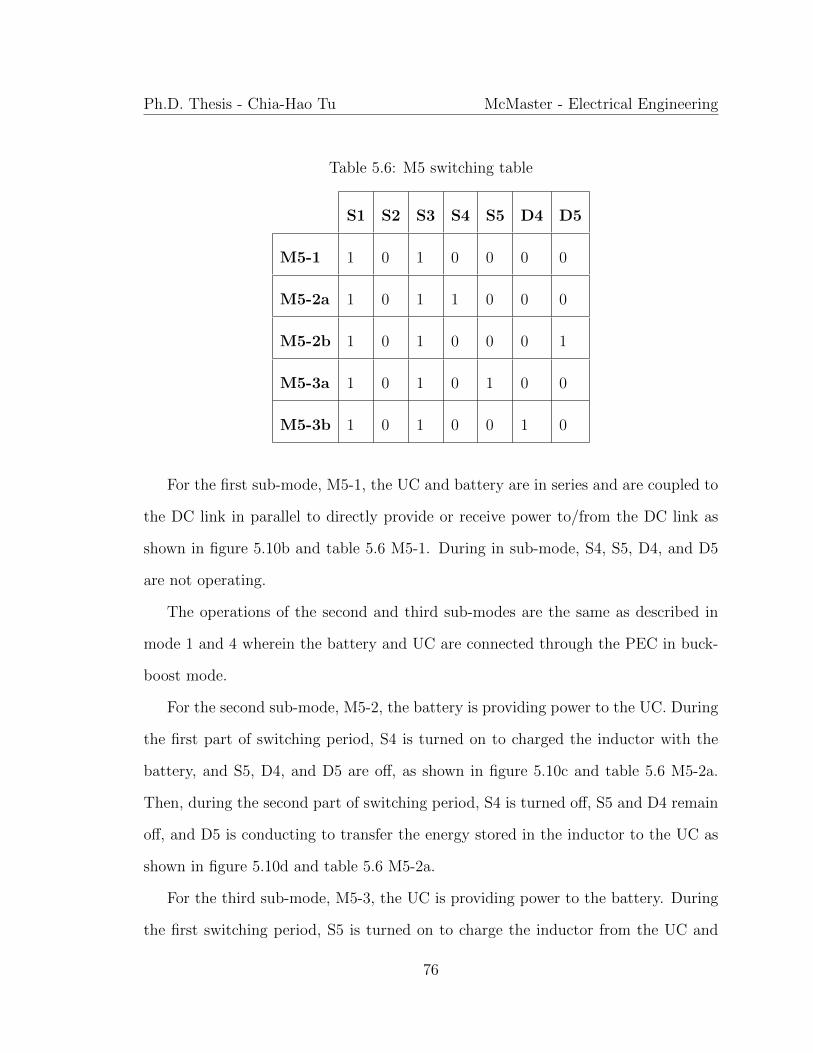
Ph.D. Thesis - Chia-Hao Tu McMaster - Electrical Engineering
Table 5.6: M5 switching table
S1 S2 S3 S4 S5 D4 D5
M5-1 1 0 1 0 0 0 0
M5-2a 1 0 1 1 0 0 0
M5-2b 1 0 1 0 0 0 1
M5-3a 1 0 1 0 1 0 0
M5-3b 1 0 1 0 0 1 0
For the first sub-mode, M5-1, the UC and battery are in series and are coupled to
the DC link in parallel to directly provide or receive power to/from the DC link as
shown in figure 5.10b and table 5.6 M5-1. During in sub-mode, S4, S5, D4, and D5
are not operating.
The operations of the second and third sub-modes are the same as described in
mode 1 and 4 wherein the battery and UC are connected through the PEC in buck-
boost mode.
For the second sub-mode, M5-2, the battery is providing power to the UC. During
the first part of switching period, S4 is turned on to charged the inductor with the
battery, and S5, D4, and D5 are off, as shown in figure 5.10c and table 5.6 M5-2a.
Then, during the second part of switching period, S4 is turned off, S5 and D4 remain
off, and D5 is conducting to transfer the energy stored in the inductor to the UC as
shown in figure 5.10d and table 5.6 M5-2a.
For the third sub-mode, M5-3, the UC is providing power to the battery. During
the first switching period, S5 is turned on to charge the inductor from the UC and
76
Ph.D. Thesis - Chia-Hao Tu McMaster - Electrical Engineering
DC link, and S4, D4, and D5 are off, as shown in figure 5.10e and table 5.6 M5-3a.
Then, for the second switching period, S5 is turned off and D4 conducts to transfer
the inductor energy to the battery; S4 and D5 remain off, as shown in figure 5.10f
and table 5.6 M5-3b.
5.3 Power Management and Control Strategy
Different operating modes are discussed in the previous subsections. Two distinctive
control strategies, UC sustaining and UC depletion modes can be realized. UC sus-
taining mode focuses on utilizing the parallel modes of the proposed SPR-HESS while
UC depletion mode focuses on utilizing the series modes of the proposed SPR-HESS.
In the next few subsections, example power management and control strategy that
are inspired by the distinctive operating modes of the proposed SPR-HESS will be
discussed. Lastly, special modes that are not categorized in the two example control
strategies will also be discussed.
5.3.1 Control Strategy 1 - UC Sustaining Mode
For control strategy 1 - UC sustaining mode, the controller of SPR-HESS tries to
”sustain” the UC voltage level that fits the load input voltage requirement. Parallel
modes, M2, M4-1, and M4-2, are utilized in this control strategy. A summarized table
for UC sustaining mode and its operation modes is shown in table 5.7.
77

Ph.D. Thesis - Chia-Hao Tu McMaster - Electrical Engineering
Table 5.7: Control strategy 1 - UC sustaining mode.
Idle Propulsion Regeneration
M2M2
M4-1 M4-2
Figure 5.11 shows an example power management that can be used for the control
strategy, wherein the controller looks at the voltage level of the UC and then adjusts
the system’s operation modes and PEC power using hysteresis loops. In this power
management example, the default operation mode for the system is M2 for propulsion,
regeneration, or idle operations of the load, where the UC is directly connected to the
load to provide power without battery’s support; in this case, the operating range for
M2 is in between 55% to 100% of the max UC voltage. During regeneration, if the
UC voltage level is at 90%, then the system operation mode becomes M4-2, wherein
the PEC charges the battery at a constant power until UC voltage level falls to its
80%; the operating range for M4-2 is in between 80% to 100% of the max UC voltage.
On the other hand, during propulsion, if the UC voltage level is at 55%, then the
system operation mode changes to M4-1, wherein the PEC discharges the battery at
a constant power to support the UC until its voltage level goes back up to its 70%;
the operating range for M4-1 is in between 70% of the max UC voltage and the load’s
minimal voltage requirement.
Such control strategy can be applied to, for example, electrified vehicle applica-
tions that have long-distance and unknown drive cycles.
78

Ph.D. Thesis - Chia-Hao Tu McMaster - Electrical Engineering
Figure 5.11: Example power management for control strategy - ultracapacitor sus-taining mode.
5.3.2 Control Strategy 2 - UC Depletion Mode
For control strategy 2 - UC depletion mode, the SPR-HESS is configured to be in
series mode as the default operating mode to ”deplete” the UC energy; modes M5-
1, M3a-1, M3a-2, M3a-3, and M3a-4 are utilized in this control strategy. The UC
depletion mode and its operation modes are summarized in table 5.8.
Table 5.8: Control strategy 2 - UC depletion mode.
Idle Propulsion Regeneration
M5-1
M5-1
M3a-1 M3a-2
M3a-3 M3a-4
79

Ph.D. Thesis - Chia-Hao Tu McMaster - Electrical Engineering
Figure 5.12 shows an example power management that can be used for the UC
depletion mode control strategy. Similar to the power management example provided
previously for UC sustaining mode, the controller monitors the voltage level of the
UC and then adjusts the system’s operation modes and PEC power. In this case, the
default operation mode of the SPR-HESS system is M5-1 for propulsion, regeneration,
or idle operations of the load. UC and battery are connected directly in series during
M5-1, as discussed in previous subsections; the operating range for M5-1 is in between
5% to 100% of the max UC voltage. When the UC voltage falls below 5%, the
controller disconnects the UC and then switches the system operation mode to M3a,
wherein the battery is the sole operating energy storage of the system; depending on
the load voltage requirement at the moment of mode changing, for propulsion, M3a-1
(PEC in boost mode) or M3a-3 (battery direct mode) are used; as for regeneration,
M3a-2 (PEC in buck mode) or M3a-4 (battery direct mode) are used.
Figure 5.12: Example power management for control strategy - UC depletion mode.
80

Ph.D. Thesis - Chia-Hao Tu McMaster - Electrical Engineering
Unlike control strategy 1, control strategy 2 can be better applied to other appli-
cations that have fixed drive cycles such as electrified public transportations, so that
the UC can be sized properly for the drive cycle, and the UC can be charged at each
end of each drive cycle.
5.3.3 Special Modes
Special modes are the operation modes that are not utilized in the two aforemen-
tioned control strategies, but can be utilized under certain circumstances and fault
conditions. A summary of these operation modes is given in table 5.9; those operation
modes are, namely, two sub-modes from mode 1 (M1-1 and M1-2), two sub-modes
from mode 3 variation b (M3b-1 and M3b-2), and two sub-mode from mode 5 (M5-2
and M5-3).
M1-1 and M1-2 from mode 1, in the application of electrified vehicle, can be used
when the load has no power demand or supply such as when the vehicle stops at a red
traffic light or when idling. Since mode 1 disconnects the load from the SPR-HESS
mentioned in previous subsections, the battery and the UC can transfer energy to
each other via the PEC in buck-boost mode depending on the decision made by the
controller and the state of charge of each energy storage component.
M3b-1 and M3b-2 from mode 3 variation b are battery only modes, wherein the
PEC is in buck-boost mode. They can be used when the UC is disconnected from the
SPR-HESS such as when the UC has a fault and cannot be used. For example, for
an electrified vehicle application that uses control strategy 1 - UC sustaining mode,
when the UC is out of service because of a fault, M3b-1 or M3b-2 modes are activated
so that the vehicle can continue to operate with battery as the sole energy source.
81
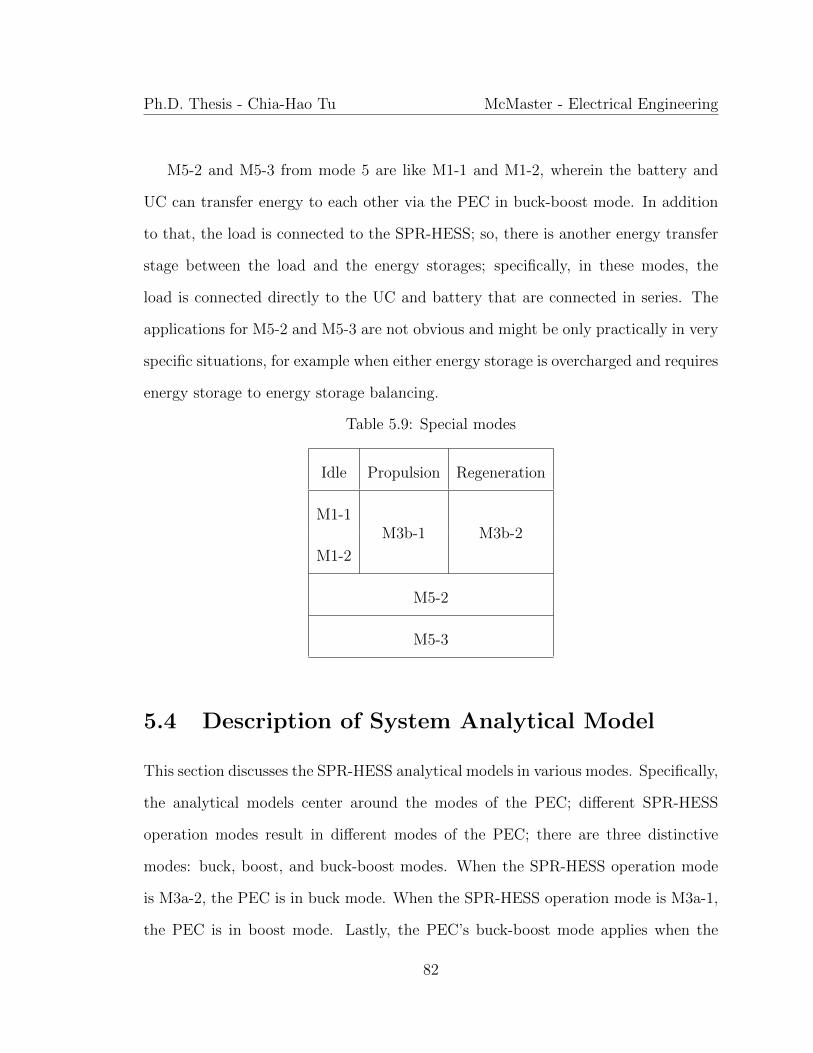
Ph.D. Thesis - Chia-Hao Tu McMaster - Electrical Engineering
M5-2 and M5-3 from mode 5 are like M1-1 and M1-2, wherein the battery and
UC can transfer energy to each other via the PEC in buck-boost mode. In addition
to that, the load is connected to the SPR-HESS; so, there is another energy transfer
stage between the load and the energy storages; specifically, in these modes, the
load is connected directly to the UC and battery that are connected in series. The
applications for M5-2 and M5-3 are not obvious and might be only practically in very
specific situations, for example when either energy storage is overcharged and requires
energy storage to energy storage balancing.
Table 5.9: Special modes
Idle Propulsion Regeneration
M1-1M3b-1 M3b-2
M1-2
M5-2
M5-3
5.4 Description of System Analytical Model
This section discusses the SPR-HESS analytical models in various modes. Specifically,
the analytical models center around the modes of the PEC; different SPR-HESS
operation modes result in different modes of the PEC; there are three distinctive
modes: buck, boost, and buck-boost modes. When the SPR-HESS operation mode
is M3a-2, the PEC is in buck mode. When the SPR-HESS operation mode is M3a-1,
the PEC is in boost mode. Lastly, the PEC’s buck-boost mode applies when the
82

Ph.D. Thesis - Chia-Hao Tu McMaster - Electrical Engineering
SPR-HESS operation mode is M1-1, M1-2, M3b-1, M3b-2, M4-1, M4-2, M5-2, or
M5-3. The small-signal models derived are the linearized models; transfer functions
then can be derived using linear control theory. The rest of the SPR-HESS operation
modes, that are not mentioned here, are direct modes wherein the ESSs are connected
with the load directly without utilizing the PEC.
5.4.1 Buck Mode
Figure 5.13 shows the circuit of SPR-HESS in buck mode during M3a-2 operation.
The analysis of this buck mode equivalent circuit for the SPR-HESS begins by making
the following assumptions:
1. This buck mode circuit is operating in steady-state.
2. The power inductor current is always positive (> 0).
3. There is an input capacitor of the circuit that is large enough to hold the input
voltage constant during steady-state operation.
4. The output capacitor of the circuit (at the battery terminals) is large enough
to hold the output voltage constant during steady-state operation.
5. The switching period is T; during time dT, switch S2 is closed; during time
(1-d)T, switch S2 is open.
6. The components are ideal.
83

Ph.D. Thesis - Chia-Hao Tu McMaster - Electrical Engineering
Figure 5.13: Buck mode circuit.
Figure 5.14 shows the equivalent circuit of the system in buck mode when the
switch S2 is closed. The DC link here is modeled as a constant DC voltage source
as the system is in regenerative mode, wherein the load-side of the system is acting
as the source; the capacitor as the DC-link is assumed to be able to hold the voltage
level during steady-state operation.
Figure 5.14: Buck mode equivalent circuit for the switch closed.
84

Ph.D. Thesis - Chia-Hao Tu McMaster - Electrical Engineering
Equations (5.1) and (5.3) show the KVL and KCL, respectively, of the equivalent
circuit during the time when S2 is closed; plugging the variable expressions (5.2) and
(5.4) into their coresponding KVL and KCL equations, the resulting circuit expres-
sions are shown in (5.5).
0 ≤ t ≤ dT
S2: closed
S1, D1, D2: open
vin = vL + vC (5.1) vC = iBRB + vB
vL = LdiLdt
(5.2)
iL = iC + iB (5.3)iin = iL
iB = vC−vBRB
iC = C dvCdt
(5.4)
(LdiLdt
)0≤t≤dT = vin − vC = vin − (iBRB + vB)
(C dvCdt
)0≤t≤dT = iL − vC−vBRB
(5.5)
Figure 5.15 shows the equivalent circuit of buck mode when the switch S2 is open.
Figure 5.15: Buck mode equivalent circuit for the switch open.
85

Ph.D. Thesis - Chia-Hao Tu McMaster - Electrical Engineering
For when S2 is open, new sets of KVL and KCL expressions are derived as shown
in equations (5.6) and (5.8), respectively. Then individual variable expressions are
derived, as shown in equations (5.7) and (5.9), and plugged back into their corre-
sponding KVL and KCL expressions to obtain the final circuit equations shown in
equation (5.10).
dT ≤ t ≤ T
D1: closed
S1, S2, D2: open
vL = −vC (5.6) vC = iBRB + vB
vL = LdiLdt
(5.7)
iL = iC + iB (5.8) iB = vC−vBRB
iC = C dvCdt
(5.9)
(LdiLdt
)dT≤t≤T = −vC = −(iBRB + vB)
(C dvCdt
)dT≤t≤T = iL − vC−vBRB
(5.10)
The final circuit expressions from the two switching times are then combined
together to make averaged circuit expressions to describe the SPR-HESS system in
buck mode.
First, the final circuit expressions obtained previously, equations (5.5) and (5.10),
are redefined by applying their corresponding switching time frame, dT and (1-d)T.
As a result, the individual sets of circuit final expressions are re-written as equations
(5.11) and (5.12).
86

Ph.D. Thesis - Chia-Hao Tu McMaster - Electrical Engineering
dTLdiLdt
= dTvin − dTvC = dTvin − dT (iBRB + vB)
dTC dvCdt
= dT iL − dT vC−vBRB
(5.11)
(1 − d)TLdiLdt
= −(1 − d)TvC = −(1 − d)T (iBRB + vB)
(1 − d)TC dvCdt
= (1 − d)TiL − (1 − d)T vC−vBRB
(5.12)
Then, the expressions can be further reduced, to equations (5.13) and (5.14).
dLdiLdt
= dvin − dvC = dvin − d(iBRB + vB)
dC dvCdt
= diL − dvC−vBRB
(5.13)
(1 − d)LdiLdt
= −(1 − d)vC = −(1 − d)(iBRB + vB)
(1 − d)C dvCdt
= (1 − d)iL − (1 − d)vC−vBRB
(5.14)
Finally, by adding expressions (5.13) and (5.14) together, we can obtain the aver-
aged expression, as shown in equation (5.15), of the buck mode circuit. With these
averaged expressions of the circuit, large signal and small signal expressions can then
be obtained by expanding the average expressions further using small and large sig-
nal variables shown in (5.16). General relationship between the input and output
of the converter can be observed by looking at the large signal expressions; on the
other hand, using small signal expressions, transfer functions of the system can be
obtained, compensator can be then designed to control the converter.
LdiLdt
= dvin − vC = dvin − (iBRB + vB)
C dvCdt
= iL − vC−vBRB
(5.15)
87

Ph.D. Thesis - Chia-Hao Tu McMaster - Electrical Engineering
iL = IL + iL
iB = IB + iB
vin = Vin + vin
vC = VC + vC
vB = VB + vB
d = D + d
(5.16)
Substituting above variable definitions in (5.15), expanded expressions are formed.
Ld(IL+iL)
dt= (D + d)(Vin + vin) − (VC + vC)
= (D + d)(Vin + vin) − [(IB + iB)RB + (VB + vB)]
C d(VC+vC)dt
= (IL + iL) − [ (VC+vC)−(VB+vB)RB
]
(5.17)
Then, (5.17) can be further reduced and reorganized into (5.18).
Ld(IL+iL)
dt= DVin +Dvin + dVin + dvin − VC − vC
= DVin +Dvin + dVin + dvin − IBRB − iBRB − VB − vB
C d(VC+vC)dt
= (IL + iL) − [ (VC−VB)+(vC−vB)RB
]
(5.18)
From (5.18), large and small signal expressions can be individually extracted.
Large signal expression:
Because the variables in large signal expressions are constant, the derivatives become
zeros due to no change. (5.19) shows the derivations for input and output voltage
relationship; on the other hand, (5.20) shows the derivations for the input and output
88

Ph.D. Thesis - Chia-Hao Tu McMaster - Electrical Engineering
current relationship.
LdIL
dt= DVin − VC = DVin − IBRB − VB = 0
∴ VC = DVin
∴ D = VC
Vin
(5.19)
C dIL
dt= IL − (VC−VB)
RB= 0
∴ IL = (VC−VB)RB
= IB
IL = DIin
(5.20)
Small signal expression:
Small signal expressions consist of variations about the steady-state operating point
(variables small hats). Therefore, the voltage and current small signal expressions
can be shown in 5.21 and 5.23. Because the varying variables are much smaller than
DC variables, the multiple of two small signal variables becomes very small and close
to zero. Thus, the multiples of any two small signal variables are approximately zero
for easier analysis. In addition, because of the assumptions made in the beginning of
the section that the input and output voltages are constant, their small signal parts
are set to zeros as shown in (5.22).
L diLdt
= Dvin + dVin + dvin − iBRB − vB
= Dvin + dVin + dvin − vC
(5.21)
89

Ph.D. Thesis - Chia-Hao Tu McMaster - Electrical Engineering
vB = 0
vin = 0
dvin = 0
L diLdt
= dVin − iBRB
= dVin − vC
vC = iBRB
(5.22)
CdvCdt
= iL − (vC − vB)
RB
= iL − vCRB
(5.23)
Equations (5.24) show the expressions (5.22) and (5.23) in s-domain, which will
then be used for obtaining transfer functions of the system and designing controllers.
sLIL(s) = d(s)Vin − VC(s)
sCVC(s) = IL(s) − VC(s)RB
(5.24)
Voltage control transfer function:
From the first line of (5.24), a new expression for IL(s) can be rearranged into (5.25).
IL(s) =d(s)Vin − VC(s)
sL(5.25)
Then, plugging the IL(s) back into the second line of (5.24), equation (5.26) is
derived.
sCVC(s) =d(s)Vin − VC(s)
sL− VC(s)
RB
(5.26)
Lastly, from equation (5.26), a transfer function for the output capacitor voltage
to duty ratio can be derived as shown step-by-step in (5.27); as a result, the final
90

Ph.D. Thesis - Chia-Hao Tu McMaster - Electrical Engineering
transfer function expression is shown as (5.28).
sCVC(s) = d(s)Vin
sL− VC(s)
sL− VC(s)
RB
sCVC(s) + VC(s)sL
+ VC(s)RB
= d(s)Vin
sL
VC(s)(sC + 1sL
+ 1RB
) = d(s)Vin
sL
VC(s)
d(s)= Vin
sL(sC+ 1sL
+ 1RB
)
(5.27)
VC(s)
d(s)=
Vin
s2LC + LRBs+ 1
(5.28)
Current control transfer function:
Because during buck mode the output of the converter is connected with the battery,
some current control is necessary. From (5.22), it is known that vC = iBRB; therefore,
(5.28) becomes (5.29) which then can be used to obtain a transfer function for the
relationship between the output capacitor voltage and battery current that is shown
as (5.30).
iB(s)RB
d(s)=
Vin
s2LC + LRBs+ 1
(5.29)
iB(s)
d(s)=
1
RB
Vin
s2LC + LRBs+ 1
(5.30)
Multiply (5.28) and (5.30) together, a transfer function that expresses the rela-
tionship between the battery current and duty cycle can then be obtained, as shown
in (5.31).
91

Ph.D. Thesis - Chia-Hao Tu McMaster - Electrical Engineering
IB(s)
VC(s)
VC(s)
d(s)= −(sC +
1
sL)
Vin
s2LC + LRBs+ 1
= − s2LCVin + Vin
s3L2C + L2
RBs2 + sL
(5.31)
5.4.2 Boost Mode
Figure 5.16 shows the circuit of SPR-HESS in boost mode during M3a-1 operation.
The analysis of this boost mode equivalent circuit for the SPR-HESS begins by making
the following assumptions:
1. This boost mode circuit is operating in steady-state.
2. The power inductor current is always positive (> 0).
3. The battery is able to hold its voltage constant during steady-state operation.
4. The output capacitor of the circuit is large enough to hold the output voltage
constant during steady-state operation.
5. The switching period is T; during time dT, switch S1 is closed; during time
(1-d)T, switch S1 is open.
6. The components are ideal.
92
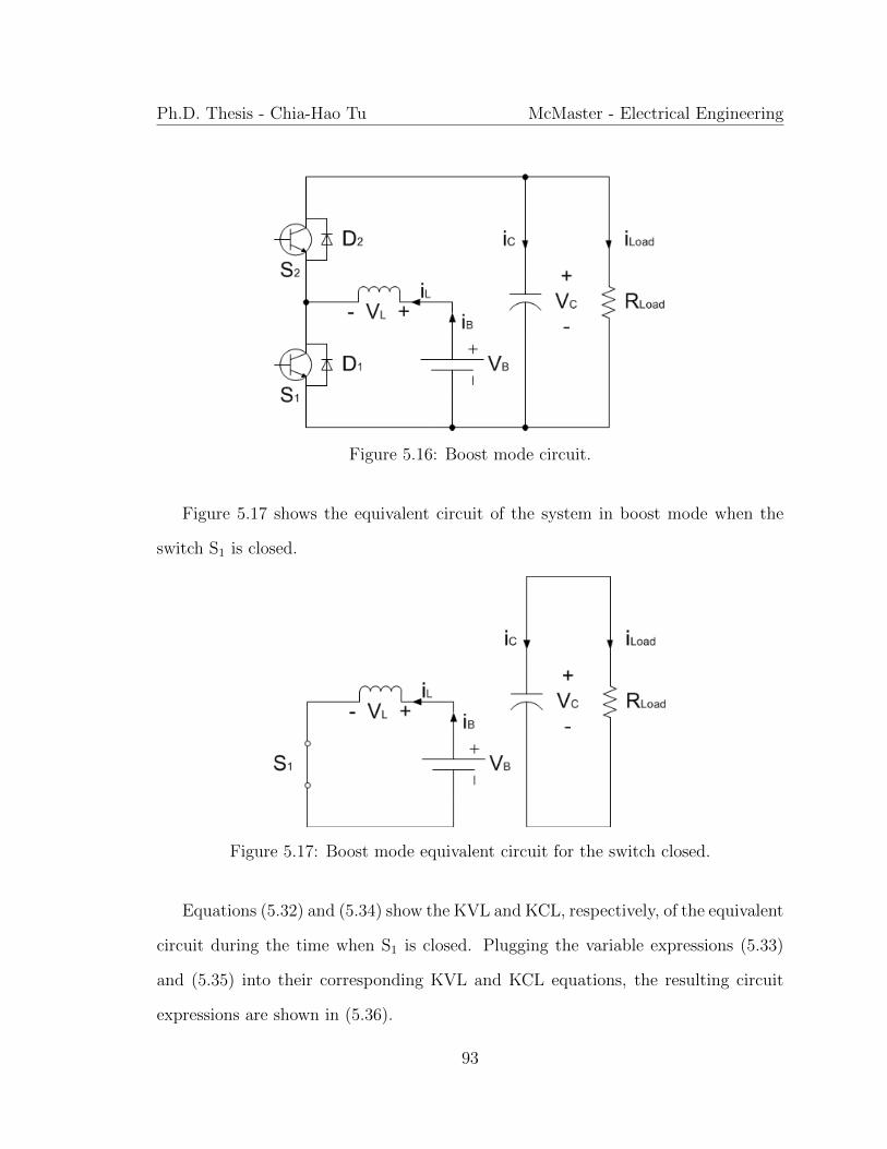
Ph.D. Thesis - Chia-Hao Tu McMaster - Electrical Engineering
Figure 5.16: Boost mode circuit.
Figure 5.17 shows the equivalent circuit of the system in boost mode when the
switch S1 is closed.
Figure 5.17: Boost mode equivalent circuit for the switch closed.
Equations (5.32) and (5.34) show the KVL and KCL, respectively, of the equivalent
circuit during the time when S1 is closed. Plugging the variable expressions (5.33)
and (5.35) into their corresponding KVL and KCL equations, the resulting circuit
expressions are shown in (5.36).
93

Ph.D. Thesis - Chia-Hao Tu McMaster - Electrical Engineering
0 ≤ t ≤ dT
S1: closed
S2, D1, D2: open
vB = vL (5.32)
vL = LdiLdt
(5.33) iL = iB
iC = −iLoad(5.34)
iLoad = vCRLoad
iC = C dvCdt
(5.35)
(LdiLdt
)0≤t≤dT = vB
(C dvCdt
)0≤t≤dT = − vCRLoad
(5.36)
Figure 5.18 shows the equivalent circuit of the system in boost mode when the
switch S1 is open.
Figure 5.18: Boost mode equivalent circuit for the switch open.
94

Ph.D. Thesis - Chia-Hao Tu McMaster - Electrical Engineering
When S1 is open, new sets of KVL and KCL expressions are derived as shown
in equations (5.37) and (5.39), respectively. Plugging the variable expressions (5.38)
and (5.40) back into their corresponding KVL and KCL expressions, the resulting
circuit expressions are shown in (5.41).
dT ≤ t ≤ T
D2: closed
S1, S2, D1: open
vB = vC + vL (5.37)
vL = LdiLdt
(5.38)
iL = iC + iLoad (5.39) iLoad = vCRLoad
iC = C dvCdt
(5.40)
(LdiLdt
)dT≤t≤T = vB − vC
(C dvCdt
)dT≤t≤T = iL − vCRLoad
(5.41)
The final circuit expressions from the two switching times are then combined to-
gether to make averaged circuit expressions to describe the system in boost mode.
The same procedure as described in the previous subsection for buck mode is used;
first the circuit expressions for the two switching times are multiplied by their corre-
sponding switching time frame ((5.42) and (5.43)), dT and (1-d)T. Then, the resulting
expressions are added together to form the averaged circuit expressions, (5.46). Such
procedure to obtain the averaged circuit expressions can be found in the following
sets of equations.
95

Ph.D. Thesis - Chia-Hao Tu McMaster - Electrical Engineering
dTLdiLdt
= dTvB
dTC dvCdt
= −dT vCRLoad
(5.42)
(1 − d)TLdiLdt
= (1 − d)T (vB − vC)
(1 − d)TC dvCdt
= (1 − d)T (iL − vCRLoad
)(5.43)
dLdiLdt
= dvB
dC dvCdt
= −d vCRLoad
(5.44)
(1 − d)LdiLdt
= (1 − d)(vB − vC)
(1 − d)C dvCdt
= (1 − d)(iL − vCRLoad
)(5.45)
LdiLdt
= vB − (1 − d)vC
C dvCdt
= (1 − d)iL − vCRLoad
(5.46)
Then, using variable definitions shown in (5.47) with the averaged circuit expres-
sions described in (5.46), the averaged circuit expressions can be expanded into (5.48),
and the large and small signal expressions can be extracted for further analysis which
is shown as (5.48).
iL = IL + iL
vB = VB + vB
vC = VC + vC
d = D + d
(5.47)
96

Ph.D. Thesis - Chia-Hao Tu McMaster - Electrical Engineering
Ld(IL+iL)dt
= (VB + vB) − (1 −D − d)(VC + vC)
= VB + vB − VC − vC +DVC +DvC + dVC + dvC
C d(VC+vC)dt
= (1 −D − d)(IL + iL) − (VC+vC)RLoad
= IL + iL −DIL −DiL − dIL − diL − (VC+vC)RLoad
(5.48)
Large signal expression:
The variables in large signal expressions are constant, resulting in zero derivatives.
From (5.48), large signal derivations for the input and output voltage and current
relationships can be obtained and shown in (5.49) and (5.50), respectively.
LdIL
dt= VB − VC +DVC = 0
∴ VC = VB
1−D
∴ D = VC−VB
VC
(5.49)
C dVC
dt= IL −DIL − VC
RLoad= 0
∴ VC
RLoad= (1 −D)IL = ILoad
∴ D = IL−ILoad
IL
(5.50)
Small signal expression:
Small signal expressions shown in (5.51) consist of small variations about the steady-
state operation which can be obtained from (5.48).
L diLdt
= vB − vC +DvC + dVC + dvC
C dvCdt
= iL −DiL − dIL − diL − vCRLoad
(5.51)
Because the small signal variables are relatively much smaller than large signal
variables, multiple of two small signal variables is approximated to zero for easier
analysis; also, the input (battery) voltage is assumed to be constant; so, its small
97

Ph.D. Thesis - Chia-Hao Tu McMaster - Electrical Engineering
signal variable is set to zero. Applying the aforementioned assumptions to (5.51),
small signal derivations can be obtained and are shown in (5.52) and (5.53).
vB = 0
dvC = 0
∴ L diLdt
= −vC +DvC + dVC = −(1 −D)vC + dVC
(5.52)
diL = 0
∴ C dvCdt
= iL −DiL − dIL − vCRLoad
= (1 −D)iL − dIL − vCRLoad
(5.53)
s-Domain of the small signal expressions, (5.54), can then be derived for obtaining
the system transfer function for controller design.
sLIL(s) = −(1 −D)VC(s) + d(s)VC
sCVC(s) = (1 −D)IL(s) − d(s)IL − VC(s)RLoad
(5.54)
Voltage control transfer function:
From the first line of (5.54), IL(s) can be re-written as (5.55).
IL(s) =−(1 −D)VC(s) + d(s)VC
sL(5.55)
Then, plugging (5.55) into the second line of (5.54), output capacitor voltage
transfer function can be derived step-by-step, as shown in (5.56). As a result, the
finalized output voltage transfer function is obtained, (5.57).
98

Ph.D. Thesis - Chia-Hao Tu McMaster - Electrical Engineering
sCVC(s) = (1 −D) [−(1−D)VC(s)+d(s)VC ]sL
− d(s)IL − VC(s)RLoad
sCVC(s) = [−(1−D)2VC(s)+(1−D)d(s)VC ]sL
− d(s)IL − VC(s)RLoad
sCVC(s) + (1−D)2VC(s)sL
+ VC(s)RLoad
= (1−D)d(s)VC
sL− d(s)IL
(sC + (1−D)2
sL+ 1
RLoad)VC(s) = ( (1−D)VC
sL− IL)d(s)
VC(s)
d(s)=
(1−D)VCsL
−IL
sC+(1−D)2
sL+ 1
RLoad
VC(s)
d(s)= (1−D)VC−sLIL
s2LC+(1−D)2+ LRLoad
s
(5.56)
VC(s)
d(s)=
−sLIL + (1 −D)VC
s2LC + LRLoad
s+ (1 −D)2(5.57)
Unlike the previous case where the battery is being charged by a source, there is
no need for battery current control; output voltage control is suffice. Therefore, the
current transfer function in this case is not derived.
5.4.3 Buck-Boost Mode
When SPR-HESS is in M1-1, M1-2, M3b-1, M3b-2, M4-1, M4-2, M5-2, or M5-3, the
PEC is in buck-boost mode. There are three variations of buck-boost mode as shown
in table 5.10.
Table 5.10: PEC Buck-boost Mode Variations Table
PEC Buck-boost Variations SPR-HESS Operation Modes
Variation 1 M3b-1, M4-1, or M5-2
Variation 2 M1-1
Variation 3 M1-2, M3b-2, M4-2, or M5-3
99

Ph.D. Thesis - Chia-Hao Tu McMaster - Electrical Engineering
The analysis of the three buck-boost equivalent circuits shown in figures 5.19,
5.22, and 5.25 begins by making the following assumptions:
1. The buck-boost mode circuits are operating in steady-state.
2. The power inductor current is always positive (> 0) in any variation.
3. The battery is able to hold its voltage constant during steady-state operation
in any variation.
4. The battery internal series resistance is not considered when it is acting as a
constant voltage source.
5. The output capacitor of the circuit is large enough to hold the output voltage
constant during steady-state operation in any variation.
6. The switching period is T. For variation 1 and 2, during time dT, switch S1 is
closed; during time (1-d)T, switch S1 is open. As for variation 3, during time
dT, switch S2 is closed; during time (1-d)T, switch S2 is open.
7. The components are ideal in any variation.
Figure 5.19 shows the PEC in buck-boost mode variation 1 when the SPR-HESS
is in M3b-1, M4-1, or M5-2 mode.
100

Ph.D. Thesis - Chia-Hao Tu McMaster - Electrical Engineering
Figure 5.19: Buck-boost mode circuit - variation 1.
Figure 5.20 shows the equivalent circuit when switch S1 is closed.
Figure 5.20: Buck-boost mode equivalent circuit for the switch closed - variation 1.
Equations (5.58) and (5.60) show the KVL and KCL of the equivalent circuit
during the time when S1 is closed. Plugging the variable expressions (5.59) and (5.61)
into their corresponding KVL and KCL equations, the resulting circuit expressions
are shown in (5.62).
0 ≤ t ≤ dT
101

Ph.D. Thesis - Chia-Hao Tu McMaster - Electrical Engineering
S1: closed
S2, D1, D2: open
vB = vL (5.58)
vL = LdiLdt
(5.59)
iL = iB
iC = −iLoad(5.60)
iC = C dvCdt
iLoad = vCRLoad
(5.61)
(LdiLdt
)0≤t≤dT = vB
(C dvCdt
)0≤t≤dT = − vCRLoad
(5.62)
Figure 5.21 shows the equivalent circuit when switch S1 is open.
Figure 5.21: Buck-boost mode equivalent circuit for the switch open - variation 1.
New sets of KVL and KCL expressions, (5.63) and (5.65), are derived when S1
is open. Plugging the variable expressions (5.64) and (5.66) into their corresponding
102

Ph.D. Thesis - Chia-Hao Tu McMaster - Electrical Engineering
KVL and KCL expressions, the resulting expressions for the circuit when the switch
S1 is open are shown in (5.67).
dT ≤ t ≤ T
D2: closed
S1, S2, D1: open
vL = −vC (5.63)
vL = LdiLdt
(5.64)
iL = iC + iLoad (5.65)
iC = C dvCdt
iLoad = vCRLoad
(5.66)
(LdiLdt
)dT≤t≤T = −vC
(C dvCdt
)dT≤t≤T = iL − vCRLoad
(5.67)
Then the resulting expressions from the two time frames, dT and (1-d)T, can be
combined to obtain average expressions of the circuit to describe the system in buck-
boost mode variation 1. First, the resulting expressions that are previously found,
(5.62) and (5.67), are multiplied by their own switching time frames, dT and (1-d)T
respectively; as a result, (5.68) and (5.69) are formed. Then, they are added together
103

Ph.D. Thesis - Chia-Hao Tu McMaster - Electrical Engineering
to obtain the averaged expressions shown in (5.70).
dTLdiLdt
= dTvB
dLdiLdt
= dvB
dTC dvCdt
= −dT vCRLoad
dC dvCdt
= −d vCRLoad
(5.68)
(1 − d)TLdiLdt
= −(1 − d)TvC
(1 − d)LdiLdt
= −(1 − d)vC
(1 − d)TC dvCdt
= (1 − d)T (iL − vCRLoad
)
(1 − d)C dvCdt
= (1 − d)(iL − vCRLoad
)
(5.69)
LdiLdt
= dvB − (1 − d)vC
C dvCdt
= − vCRLoad
+ (1 − d)iL
(5.70)
Using variable definitions in (5.71), the averaged circuit expressions can be ex-
panded into (5.72), which consists of large and small signal expressions that can be
used for further analysis.
iL = IL + iL
vB = VB + vB
vC = VC + vC
d = D + d
(5.71)
104

Ph.D. Thesis - Chia-Hao Tu McMaster - Electrical Engineering
Ld(IL+iL)dt
= (D + d)(VB + vB) − (1 −D − d)(VC + vC)
= DVB +DvB + dVB + dvB − VC − vC +DVC +DvC + dVC + dvC
C d(VC+vC)dt
= − (VC+vC)RLoad
+ (1 −D − d)(IL + iL)
= − VC
RLoad− vC
RLoad+ IL + iL −DIL −DiL − dIL − diL
(5.72)
Large signal expression:
Because the variables in large signal expressions are constant, their derivatives become
zeros. From (5.72), large signal expressions can be extracted to obtain the input and
output current and voltage relationships which are shown in (5.73) and (5.74).
LdIL
dt= DVB − VC +DVC = 0
∴ VC = D1−D
VB
∴ D = VC
VC+VB
(5.73)
C dVC
dt= − VC
RLoad+ IL −DIL = 0
∴ VC
RLoad= ILoad = (1 −D)IL
∴ D = IL−ILoad
IL
(5.74)
Small signal expression:
From (5.72), small signal expressions can also be obtained, which are shown in (5.75).
L diLdt
= DvB + dVB + dvB − vC +DvC + dVC + dvC
C dvCdt
= − vCRLoad
+ iL −DiL − dIL − diL
(5.75)
The input voltage of the converter, battery voltage, is assumed to be constant;
so, its small signal variable is zero. In addition, because the small signal variables are
105

Ph.D. Thesis - Chia-Hao Tu McMaster - Electrical Engineering
small, multiple of two small signal variables becomes very close to zero thus negligible.
Therefore, (5.75) becomes (5.76) and (5.77).
dvB = 0
vB = 0
∴ L diLdt
= dVB − vC +DvC + dVC = d(VB + VC) − (1 −D)vC
(5.76)
diL = 0
∴ C dvCdt
= − vCRLoad
+ iL −DiL − dIL = (1 −D)iL − vCRLoad
− dIL
(5.77)
Small signal expressions, (5.78), in s-domain can then be obtained.
sLIL(s) = d(s)(VB + VC) − (1 −D)VC(s)
sCVC(s) = (1 −D)IL(s) − VC(s)RLoad
− d(s)IL
(5.78)
Voltage control transfer function:
From the first line of (5.78), IL(s) can be re-written as (5.79).
IL(s) =d(s)(VB + VC) − (1 −D)VC(s)
sL(5.79)
Then, (5.79) can be plugged into the second line of (5.78) which can then be
used to derive the output capacitor voltage transfer function for controller design.
The following equations shown in (5.80) illustrate the step-by-step derivation of the
transfer function, and (5.81) is the resulting transfer function.
106

Ph.D. Thesis - Chia-Hao Tu McMaster - Electrical Engineering
sCVC(s) = (1−D)[d(s)(VB+VC)−(1−D)VC(s)]sL
− VC(s)RLoad
− d(s)IL
sCVC(s) = (1−D)d(s)(VB+VC)sL
− (1−D)2VC(s)sL
− VC(s)RLoad
− d(s)IL
sCVC(s) + (1−D)2VC(s)sL
+ VC(s)RLoad
= (1−D)d(s)(VB+VC)sL
− d(s)IL
VC(s) =(1−D)d(s)(VB+VC )
sL−d(s)IL
sC+(1−D)2
sL+ 1
RLoad
= (1−D)d(s)(VB+VC)−d(s)ILsL
s2LC+(1−D)2+ LRLoad
s
(5.80)
VC(s)
d(s)=
−ILLs+ (1 −D)(VB + VC)
s2LC + LRLoad
s+ (1 −D)2(5.81)
Figure 5.22 shows the system circuit with PEC in buck-boost mode variation 2,
and figure 5.23 shows the equivalent circuit of the system when switch S1 is closed.
Figure 5.22: Buck-boost mode circuit - variation 2.
Figure 5.23: Buck-boost mode equivalent circuit for the switch closed - variation 2.
107
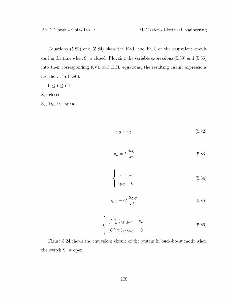
Ph.D. Thesis - Chia-Hao Tu McMaster - Electrical Engineering
Equations (5.82) and (5.84) show the KVL and KCL or the equivalent circuit
during the time when S1 is closed. Plugging the variable expressions (5.83) and (5.85)
into their corresponding KVL and KCL equations, the resulting circuit expressions
are shown in (5.86).
0 ≤ t ≤ dT
S1: closed
S2, D1, D2: open
vB = vL (5.82)
vL = LdiLdt
(5.83)
iL = iB
iUC = 0(5.84)
iUC = CdvUC
dt(5.85)
(LdiLdt
)0≤t≤dT = vB
(C dvucdt
)0≤t≤dT = 0(5.86)
Figure 5.24 shows the equivalent circuit of the system in buck-boost mode when
the switch S1 is open.
108

Ph.D. Thesis - Chia-Hao Tu McMaster - Electrical Engineering
Figure 5.24: Buck-boost mode equivalent circuit for the switch open - variation 2.
During the time when S1 is open, new sets of KVL and KCL expressions are
derived as shown in equations (5.87) and (5.89). Plugging the variable expressions
(5.88) and (5.90) into their corresponding KVL and KCL expressions, the resulting
circuit expressions are shown in (5.91).
dT ≤ t ≤ T
D2: closed
S1, S2, D1: open
vL = −vUC − iUCRUC (5.87)
vL = LdiLdt
(5.88)
iL = iUC (5.89)
iUC = CdvUC
dt(5.90)
109

Ph.D. Thesis - Chia-Hao Tu McMaster - Electrical Engineering
(LdiLdt
)dT≤t≤T = −vUC − iLRUC
(C dvucdt
)dT≤t≤T = iL
(5.91)
The circuit expressions for different switching time frames can then be combined
together to generate averaged circuit expressions to describe the system in buck-
boost mode variation 2. First, the resulting expressions from (5.86) and (5.91) are
multiplied by their corresponding switching time frames, dT and (1-d)T, respectively.
As a result, (5.92) and (5.93) are obtained and then added together to get the averaged
expressions shown in (5.94).
dTLdiLdt
= dTvB
dLdiLdt
= dvB
dTC dvUC
dt= 0
dC dvUC
dt= 0
(5.92)
(1 − d)TLdiLdt
= −(1 − d)TvUC − (1 − d)TiLRUC
(1 − d)LdiLdt
= −(1 − d)vUC − (1 − d)iLRUC
(1 − d)TC dvUC
dt= (1 − d)TiL
(1 − d)C dvUC
dt= (1 − d)iL
(5.93)
LdiLdt
= dvB − (1 − d)vUC − (1 − d)iLRUC
C dvUC
dt= (1 − d)iL
(5.94)
Using the variable definitions in (5.95), the averaged circuit expressions can be
expanded into (5.96), which consists of large and small signal variables that can be
used for further analysis and control design.
110

Ph.D. Thesis - Chia-Hao Tu McMaster - Electrical Engineering
iL = IL + iL
vB = VB + vB
vUC = VUC + vUC
d = D + d
(5.95)
Ld(IL+iL)dt
= (D + d)(VB + vB) − (1 −D − d)(VUC + vUC) − (1 −D − d)(IL + iL)RUC
= DVB +DvB + dVB + dvB − VUC − vUC +DVUC +DvUC + dVUC
+dvUC − ILRUC − iLRUC +DILRUC +DiLRUC + dILRUC + diLRUC
C d(VUC+vUC)dt
= (1 −D − d)(IL + iL) = IL + iL −DIL −DiL − dIL − diL
(5.96)
Large signal expression:
From (5.96), large signal expressions can be formed to obtain the relationship between
the input and output current and voltage. Because the large signal variables are
constant, their derivatives are zeros. Expressions shown in (5.97) and (5.98) are the
results.
LdILdt
= DVB − VUC +DVUC − ILRUC +DILRUC = 0
DVB − (1 −D)VUC − (1 −D)ILRUC = 0
−(1 −D)VUC = −DVB + (1 −D)ILRUC
∴ VUC = DVB−(1−D)ILRUC
(1−D)
∴ D = VUC+ILRUC
VB+ILRUC+VUC
(5.97)
C dVUC
dt= IL −DIL = 0
IL = DIL = 0(5.98)
111

Ph.D. Thesis - Chia-Hao Tu McMaster - Electrical Engineering
Small signal expression:
From (5.96), small signal expressions, shown in (5.99), can also be formed to obtain
the transfer function of the output voltage of the system later on.
L diL
dt= DvB + dVB + dvB − vUC +DvUC + dVUC + dvUC − iLRUC +DiLRUC
+dILRUC + diLRUC
C dvUC
dt= iL −DiL − dIL − diL
(5.99)
The source voltage, battery voltage, in this mode is assumed to constant; so, its
small signal variable is set to zero. In addition, because the small signal variables are
small, multiple of two small signal variables becomes insignificant; therefore, it is set
to zero. Thus, (5.99) becomes (5.100) and (5.101), and their expressions in s-domain
are shown in (5.102).
vB = 0
dvUC = 0
diL = 0
∴ L diLdt
= dVB − vUC +DvUC + dVUC − iLRUC +DiLRUC + dILRUC
= −(1 −D)vUC − (1 −D)iLRUC + d(VB + VUC + ILRUC)
(5.100)
diL = 0
∴ C dvUC
dt= iL −DiL − dIL = (1 −D)iL − dIL
(5.101)
112

Ph.D. Thesis - Chia-Hao Tu McMaster - Electrical Engineering
sLIL(s) = −(1 −D)VUC(s) − (1 −D)IL(s)RUC + d(s)(VB + VUC + ILRUC)
sCVUC(s) = (1 −D)IL(s) − d(s)IL
(5.102)
Voltage transfer function:
From (5.102) first line, IL can be derived into (5.103).
IL(s) = −(1−D)VUC(s)−(1−D)IL(s)RUC+d(s)(VB+VUC+ILRUC)
sL
IL(s) + (1−D)IL(s)RUC
sL= −(1−D)VUC(s)+d(s)(VB+VUC+ILRUC)
sL
IL(s) = −(1−D)VUC(s)+d(s)(VB+VUC+ILRUC)
sL[1+(1−D)RUC
sL]
(5.103)
Then, plugging (5.103) into the second line of (5.102), output capacitor voltage
transfer function can be derived step-by-step as shown in (5.104), and the finalized
output transfer function is obtained and shown in (5.105). A right-half-plane (RHP)
zero, which can cause stability issues, is observed; thus, discontinuous mode of op-
eration should be used to apply discontinuous inductor current during operation to
remedy the stability problem.
113

Ph.D. Thesis - Chia-Hao Tu McMaster - Electrical Engineering
sCVUC(s) = (1 −D)(−(1−D)VUC(s)+d(s)(VB+VUC+ILRUC)
sL[1+(1−D)RUC
sL]
) − d(s)IL
sCVUC(s) + (1−D)2VUC(s)
sL[1+(1−D)RUC
sL]
= d(s)( (VB+VUC+ILRUC)(1−D)
sL[1+(1−D)RUC
sL]
− IL)
VUC(s)(sC + (1−D)2
sL[1+(1−D)RUC
sL]) = d(s)( (VB+VUC+ILRUC)(1−D)
sL[1+(1−D)RUC
sL]
− IL)
VUC(s)
d(s)=
(VB+VUC+ILRUC )(1−D)
sL[1+(1−D)RUC
sL]
−IL
sC+(1−D)2
sL[1+(1−D)RUC
sL]
VUC(s)
d(s)=
(VB+VUC+ILRUC)(1−D)−sILL[1+(1−D)RUC
sL]
s2CL[1+(1−D)RUC
sL]+(1−D)2
VUC(s)
d(s)= (VB+VUC+ILRUC)(1−D)−sILL−(1−D)RUCIL
s2CL+(1−D)RUCsC+(1−D)2
(5.104)
VUC(s)
d(s)=
−sILL+ (VB + VUC)(1 −D)
s2CL+ sC(1 −D)RUC + (1 −D)2(5.105)
Figure 5.25 shows the PEC in buck-boost mode variation 3 when the SPR-HESS
is in M1-2, M3b-2, M4-2, or M5-3 mode. Figure 5.26, shows the equivalent circuit
when switch S2 is closed.
Figure 5.25: Buck-boost mode circuit - variation 3.
114

Ph.D. Thesis - Chia-Hao Tu McMaster - Electrical Engineering
Figure 5.26: Buck-boost mode equivalent circuit for the switch closed - variation 3.
Equations (5.106) and (5.108) show the KVL and KCL of the equivalent circuit
during the time when S2 is closed. Plugging the variable expressions (5.107) and
(5.109) into their corresponding KVL and KCL equations, the resulting circuit ex-
pressions are shown in (5.110).
0 ≤ t ≤ dT
S2: closed
S1, D1, D2: open
vin = vL
vC = iBRB + vB
(5.106)
vL = LdiLdt
(5.107)
115

Ph.D. Thesis - Chia-Hao Tu McMaster - Electrical Engineering
iL = iin
iC = −iB(5.108)
iC = C dvCdt
iB = vC−vBRB
(5.109)
(LdiLdt
)0≤t≤dT = vin
(C dvCdt
)0≤t≤dT = − (vC−vB)RB
(5.110)
Figure 5.27 shows the equivalent circuit when switch S2 is open.
Figure 5.27: Buck-boost mode equivalent circuit for the switch open - variation 3.
New sets of KVL and KCL equations, (5.111) and (5.113), are derived when S2 is
open. Plugging the variable expressions (5.112) and (5.114) into their corresponding
KVL and KCL equations, the resulting expressions for the circuit are shown in (5.115).
dT ≤ t ≤ T
D1: closed
S1, S2, D2: open
vL = −vC (5.111)
116

Ph.D. Thesis - Chia-Hao Tu McMaster - Electrical Engineering
vL = LdiLdt
(5.112)
iL = iC + iB (5.113)
iC = C dvCdt
iB = vC−vBRB
(5.114)
(LdiLdt
)dT≤t≤T = −vC
(C dvCdt
)dT≤t≤T = iL − (vC−vB)RB
(5.115)
Then the resulting expressions from the two time frames, dT and (1-d)T, can
be combined to obtain average expressions of the circuit to describe the system.
First, the resulting expressions that are previously found, (5.110) and (5.115), are
multiplied by their own switching time frames, dT and (1-d)T, respectively; thus,
equations (5.116) and (5.117) are derived. Lastly, they are added together to obtain
the averaged expressions shown in (5.118).
dTLdiLdt
= dTvin
dLdiLdt
= dvin
dTC dvCdt
= −dT (vC−vB)RB
dC dvCdt
= −d (vC−vB)RB
(5.116)
117

Ph.D. Thesis - Chia-Hao Tu McMaster - Electrical Engineering
(1 − d)TLdiLdt
= −(1 − d)TvC
(1 − d)LdiLdt
= −(1 − d)vC
(1 − d)TC dvCdt
= (1 − d)TvL − (1 − d)T (vC−vB)RB
(1 − d)C dvCdt
= (1 − d)iL − (1 − d) (vC−vB)RB
(5.117)
LdiLdt
= dvin − (1 − d)vC
C dvCdt
= (1 − d)iL − (vC−vB)RB
(5.118)
Using the variable definitions shown in (5.119), the averaged circuit expressions
can be expanded into (5.120), which consists of large and small signal expressions.
vin = Vin + vin
vC = VC + vC
vB = VB + vB
iL = IL + iL
d = D + d
(5.119)
Ld(IL+iL)dt
= (D + d)(Vin + vin) − (1 −D − d)(VC + vC)
= DVin +Dvin + dVin + dvin − VC − vC +DVC +DvC + dVC + dvC
C d(VC+vC)dt
= (1 −D − d)(IL + iL) − [(VC+vC)−(VB+vB)]RB
= IL + iL −DIL −DiL − dIL − diL − VC−VB
RB− vC−vB
RB
(5.120)
Large signal expression:
From (5.120), large signal expressions can be found to extract the relationships of
the input and output voltage and current of the circuit in terms of the switching
118

Ph.D. Thesis - Chia-Hao Tu McMaster - Electrical Engineering
duty cycle, which are shown in (5.121) and (5.122). Because large signal variables are
constant, their derivatives become zeros.
L ILdt
= DVin − VC +DVC = 0
DVin − (1 −D)VC = 0
∴ VC = DVin
1−D
∴ D = VC
Vin+VC
(5.121)
C dIL
dt= IL −DIL − (VC−VB)
RB= 0; (VC−VB)
RB= IB
∴ IB = (1 −D)IL
∴ D = IL−IBIL
(5.122)
Small signal expression:
Similarly, from (5.120), small signal expressions can also be obtained, as is shown in
(5.123).
L diLdt
= Dvin + dVin + dvin − vC +DvC + dVC + dvC
C dvCdt
= iL −DiL − dIL − diL − vC−vBRB
(5.123)
The input voltage of the converter and the battery voltage are assumed to be
constant, so their small signal voltage variables become zeros. In addition, because
the small signal variables are small, multiple of two small signal variables becomes
negligible. As a result, the small signal expressions can be re-written as (5.124) and
(5.125).
119
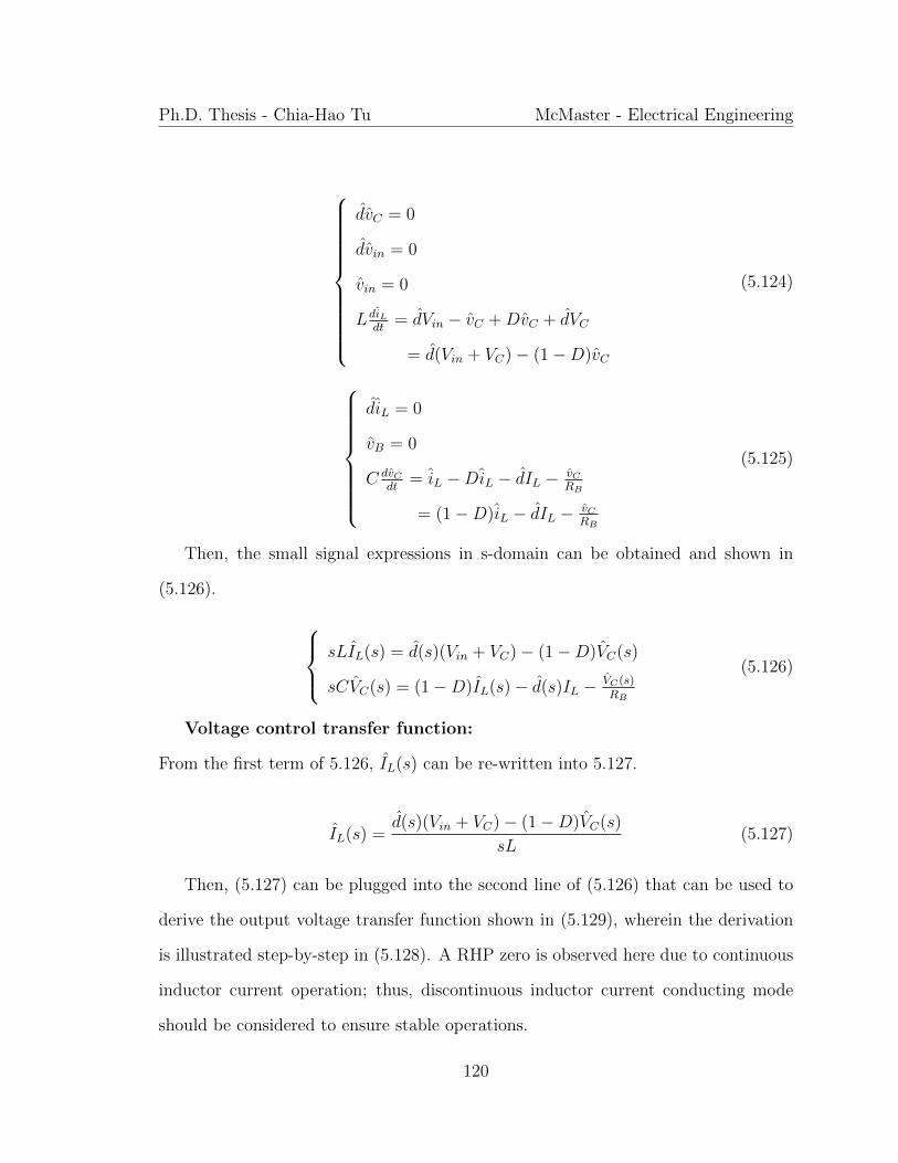
Ph.D. Thesis - Chia-Hao Tu McMaster - Electrical Engineering
dvC = 0
dvin = 0
vin = 0
L diLdt
= dVin − vC +DvC + dVC
= d(Vin + VC) − (1 −D)vC
(5.124)
diL = 0
vB = 0
C dvCdt
= iL −DiL − dIL − vCRB
= (1 −D)iL − dIL − vCRB
(5.125)
Then, the small signal expressions in s-domain can be obtained and shown in
(5.126).
sLIL(s) = d(s)(Vin + VC) − (1 −D)VC(s)
sCVC(s) = (1 −D)IL(s) − d(s)IL − VC(s)RB
(5.126)
Voltage control transfer function:
From the first term of 5.126, IL(s) can be re-written into 5.127.
IL(s) =d(s)(Vin + VC) − (1 −D)VC(s)
sL(5.127)
Then, (5.127) can be plugged into the second line of (5.126) that can be used to
derive the output voltage transfer function shown in (5.129), wherein the derivation
is illustrated step-by-step in (5.128). A RHP zero is observed here due to continuous
inductor current operation; thus, discontinuous inductor current conducting mode
should be considered to ensure stable operations.
120

Ph.D. Thesis - Chia-Hao Tu McMaster - Electrical Engineering
sCVC(s) = (1 −D) d(s)(Vin+VC)−(1−D)VC(s)sL
− d(s)IL − VC(s)RB
sCVC(s) + (1−D)2VC(s)sL
+ VC(s)RB
= (1−D)d(s)(Vin+VC)sL
− d(s)IL
VC(s)[sC + (1−D)2
sL+ 1
RB] = d(s)( (1−D)(Vin+VC)
sL− IL)
VC(s)
d(s)=
(1−D)(Vin+VC )
sL−IL
sC+(1−D)2
sL+ 1
RB
(5.128)
VC(s)
d(s)=
(1 −D)(Vin + VC) − sLIL
s2LC + LRBs+ (1 −D)2
(5.129)
Current control transfer function:
Because in this mode variation the battery is the output of the PEC, current control
is desirable. From (5.22), it is known that vC = iBRB; hence, current control transfer
function, (5.130), can be derived from (5.129).
iB(s)
d(s)=
1
RB
(1 −D)(Vin + VC) − sLIL
s2LC + LRBs+ (1 −D)2
(5.130)
5.5 Simulation Setup
5.5.1 Simulation Parameters and Specifications
Simulation studies are conducted using Autonomie and Matlab/Simulink. Table 5.11
shows the simulation parameters used. An arbitrary pure electric lightweight vehicle
model is used for the drive cycle simulation studies. The vehicle’s powertrain structure
is a pure electric and single speed reduction one with one 35kW electric motor with an
arbitrary motor inverter that can work with various input voltage levels. The hybrid
energy storage parameters for all the simulations with different HESS configuration
is a combination of a 255.3V, 10.8Ah li-ion polymer battery bank and a 288V, 13.35F
121

Ph.D. Thesis - Chia-Hao Tu McMaster - Electrical Engineering
UC bank. The overall vehicle weight is 200kg including the driver. As for PEC
simulations, the power inductor has an inductance of 1mH. The overall power of
the power electronic converter is rated at 13kW, which is the controlled battery
discharging power. The switching frequency of 1kHz is selected for convenience of
calculation and component selection for the simulation study. The efficiency of the
PEC is set to be a constant of 80% for drive cycle simulations for all the HESS
configurations.
The accuracy of the simulation models is limited. Although generic parameters
in Autonomie and Matlab/Simulink are used, real parameters from the selected com-
ponent datasheet are entered into the simulation models. However, the simulation
studies focus on validating the functionalities of the PEC and conducting compar-
ative analysis of HESS configurations; high accuracy of the simulation models in
comparison to the real-world environment is not necessary.
122

Ph.D. Thesis - Chia-Hao Tu McMaster - Electrical Engineering
Table 5.11: Simulation parameters
Specifications for Major Components
Powertrain Structure Pure electric, single speed reduction
Electric Motor Power 35kW continuous; 60kW peak @ 3,000rpm
Energy Storage 1 Li-ion Polymer 255.3V nominal, 10.8Ah
Energy Storage 2 Ultracapacitor 288V maximum, 13.35F
Motorbike Weight 200kg
PEC Simulation Parameters
Power inductor, L 1mH
Switching frequency, fs 1kHz
Maximum power 13kW
Efficiency 80%
5.5.2 Simulation Model and Control Strategy Logics
Figure 5.28: Autonomie Simulation Model.
123

Ph.D. Thesis - Chia-Hao Tu McMaster - Electrical Engineering
For top-level simulation studies, Autonomie is first used to obtain the drive cycle and
load data; the model used in the program is shown in figure 5.28. Then the data are
used for further simulation studies in the Matlab/Simulink. The Urban Dynamometer
Driving Schedule (UDDS) is used for drive cycle simulations; for these simulation
studies, the speed demand of a UDDS drive cycle is applied to the simulation model,
and the resulting power profile for this specific vehicle is shown in figure 5.29.
Figure 5.29: Urban Dynamometer Driving Schedule (UDDS) Power and Speed Profile.
The simulation model shown in figure 5.30 consists of two major functional blocks;
one is a state flow control block that implements control strategies and another one
is energy storage block that implements the HESS. Two different control strategies,
UC sustaining (shown in figure 5.31) and UC depletion (shown in figure 5.32), as well
as a mixed control strategy that combines the aforementioned two are studied using
the Matlab/Simulink simulation model.
124

Ph.D. Thesis - Chia-Hao Tu McMaster - Electrical Engineering
Figure 5.30: Simulink Simulation Model for Drive Cycle Simulations.
Figure 5.31: State-flow Control Logic for UC Sustaining Mode.
125

Ph.D. Thesis - Chia-Hao Tu McMaster - Electrical Engineering
Figure 5.32: State-flow Control Logic for UC Depletion Mode.
For more detailed PEC simulations that have higher sampling rate and shorter
simulation time to accommodate the high switching speed, five simulation models are
created to verify the functionalities of the PEC in five different modes: buck, boost,
and three variations of buck-boost modes, which are shown in figures 5.33, 5.34, 5.35,
5.36, and 5.37, respectively. PID feedback loops are used for current and voltage
controls; their parameters are derived using sisotool in Matlab. The mathematical
analysis and derivations of the PEC transfer functions in five different modes can be
found in the previous sub-sections.
Stability issues caused by RHP zero are observed in boost and buck-boost voltage
to duty ratio transfer functions in the previous analysis sub-sections. Therefore, extra
inductor current limiting logics are implemented to force the operation of inductor
discontinuous conduction mode (DCM); the results of such DCM implementation can
be observed in figures 5.39 and 5.40.
126

Ph.D. Thesis - Chia-Hao Tu McMaster - Electrical Engineering
Figure 5.33: Simulink Simulation Model for PEC in Buck Mode.
Figure 5.34: Simulink Simulation Mode for PEC in Boost Mode.
127

Ph.D. Thesis - Chia-Hao Tu McMaster - Electrical Engineering
Figure 5.35: Simulink Simulation Model for PEC in Buck-boost Mode Variation 1.
Figure 5.36: Simulink Simulation Model for PEC in Buck-boost Mode Variation 2.
128

Ph.D. Thesis - Chia-Hao Tu McMaster - Electrical Engineering
Figure 5.37: Simulink Simulation Model for PEC in Buck-boost Mode Variation 3.
5.6 Simulation Results and Discussion
5.6.1 Simulation Results of PEC Functionalities
Figure 5.38 shows the simulation results for the PEC in buck mode. When the PEC
is in buck mode, the direction of the power flow is from the load and/or from the
UC bank to the battery, hence the simulation results are showing the three major
parameters: battery SOC, current, and voltage. As shown in the plots, the simulation
lasts for 30 seconds; the battery SOC first starts at 98% and ends at around 98.27%.
The maximum charging current is limited at 10A during constant current mode (CC);
the battery voltage is strictly controlled below 289V during constant voltage mode
129

Ph.D. Thesis - Chia-Hao Tu McMaster - Electrical Engineering
(CV) and throughout the duration of the simulation.
Figure 5.38: PEC Simulation Result - Buck Mode.
Figure 5.39 shows the simulation results for the PEC in boost mode. During this
operation mode, the direction of the power flow is from the battery to the load; so,
the figure is showing the inductor current in DCM, load current, and load voltage
plots. The output of the system is loaded with a 19Ohm resistor to simulate a 10kW
load, and the target load voltage is set to be 444V, which conditions are met by
the simulation results that the settling current is around 23A with controlled output
voltage of around 444V.
130

Ph.D. Thesis - Chia-Hao Tu McMaster - Electrical Engineering
Figure 5.39: PEC Simulation Result - Boost Mode.
Figure 5.40 shows the simulation results for the PEC in buck-boost mode 1. Dur-
ing this operation mode, the direction of the power flow is from the battery to the
load which is directly connected with the UC. The figure shows the load current and
voltage that settle at around 36A and targeted 288V output voltage, respectively.
The output of the system is loaded with an 8Ohm resistor to simulate a 10kW load.
Figure 5.40: PEC Simulation Result - Buck-boost Mode v1.
131

Ph.D. Thesis - Chia-Hao Tu McMaster - Electrical Engineering
Figure 5.41 shows the simulation results for the PEC in buck-boost mode 2. Dur-
ing this operation mode, the load is disconnected from the SPR-HESS system; the
direction of the power flow is from the battery to the UC. The figure shows the UC
voltage, battery current, and inductor current plots. At the start of the simulation,
the UC is at 260V, and then it is being charged by the PEC and battery to a fi-
nal voltage of 288V. The UC charging current is limited to the battery’s discharging
capability of 200A.
Figure 5.41: PEC Simulation Result - Buck-boost Mode v2.
Figure 5.42 shows the simulation results for the PEC in buck-boost mode 3. Dur-
ing this operation mode, the battery is being charged by either or both the load and
the UC through the PEC. The figure shows the battery SOC, current, and voltage
plots. The battery SOC is set to be at 98% at the beginning of the simulation and
then charged to around 98.27%. The current and voltage plots show the controller
limiting the average battery charging current of around 10A maximum (1C) during
CC mode and voltage of 289V maximum during CV mode and the entire operation.
132

Ph.D. Thesis - Chia-Hao Tu McMaster - Electrical Engineering
Figure 5.42: PEC Simulation Result - Buck-boost Mode v3.
5.6.2 Simulation Results of SPR-HESS used for UDDS Drive
Cycle with Different Control Strategies
Figures 5.43 to 5.51 show the current, SOC, power, and voltage of the battery and
the UC under three different control strategies (UC sustaining, UC depletion, and
mixed) and two different configurations (UCFL and BFL).
In UC sustaining mode, simulated results shown in figures 5.43 and 5.44, the sys-
tem has more control over the power flow in and out of the battery due to having the
PEC active throughout the entire drive cycle. The resulting maximum battery dis-
charging current and power are successfully limited to 3.48C and 10kW, respectively;
on the other hand, the maximum UC discharging current and power are 8.96C and
16.2kW, respectively. Moreover, the battery charging current and power are equal to
zero; the maximum UC charging current and power are 3.52C and 6kW. The bat-
tery SoC starts at 90% and ends at 81.74%. The maximum UC energy utilization is
133

Ph.D. Thesis - Chia-Hao Tu McMaster - Electrical Engineering
70.66% and the maximum UC voltage variation is 45% in this control strategy.
In the case of control strategy 1 - UC sustaining mode, the SPR-HESS UCFL
configuration generates the output voltage that matches the UC’s; thus, as can be
seen in the simulation result shown in figure 5.45a, the output voltage varies from
288V to 156V. On the other hand, the SPR-HESS BFL configuration generates the
output voltage that matches the battery’s; thus, the output voltage does not vary as
much, from 276.47V to 266.24V.
134
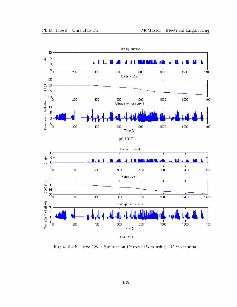
Ph.D. Thesis - Chia-Hao Tu McMaster - Electrical Engineering
(a) UCFL
(b) BFL
Figure 5.43: Drive Cycle Simulation Current Plots using UC Sustaining.
135

Ph.D. Thesis - Chia-Hao Tu McMaster - Electrical Engineering
(a) UCFL
(b) BFL
Figure 5.44: Drive Cycle Simulation Power Plots using UC Sustaining.
136

Ph.D. Thesis - Chia-Hao Tu McMaster - Electrical Engineering
(a) UCFL
(b) BFL
Figure 5.45: Drive Cycle Simulation Voltage Plots using UC Sustaining.
137

Ph.D. Thesis - Chia-Hao Tu McMaster - Electrical Engineering
In UC depletion mode, simulated results shown in figures 5.46 to 5.47, the sys-
tem first connect the battery and UC together in series connection to provide power
directly to the load to fully utilize the energy from the UC, and when the UC is de-
pleted, the system turns on the PEC and disconnects the UC so that the battery acts
as a sole energy source to the load. The trade-off of UC depletion mode is that the
PEC has no direct control over the battery during depletion mode, so the components
have to be properly sized so that the battery can handle the load power. After the
UC is depleted, the battery is the sole energy source to provide power to the load,
which is limited by the power capabilities of the PEC and the battery itself that could
influence the performance of the system if the components are not sized properly or
the control strategy is not designed properly with respect to the load requirements.
However, because the system utilizes the UC energy fully and the system provides
power to the load directly without going through the PEC for the most part of the
drive cycle, battery energy is utilized more efficiently than that in the UC sustaining
mode. As a result, the end battery SoC is 82.52%, 0.8% higher than that of the UC
sustaining mode. The resulting maximum battery discharging current and power are
3.58C and 10.3kW, respectively; on the other hand, the maximum UC discharging
current and power are 3.58C and 8kW, respectively. Moreover, the battery charging
current and power are 1.24C and 3.7kW; the maximum UC charging current and
power are 1.24C and 2.5kW. The maximum UC energy utilization is 94.16% and the
maximum UC voltage variation is 95% in this control strategy.
In the case of control strategy 2 - UC depletion mode, the output voltage of both
SPR-HESS UCFL and BFL configurations are the same, which varies from 564.47V
to 339.97V, as can be seen in figure 5.48. The reason being that in both cases, UC
138

Ph.D. Thesis - Chia-Hao Tu McMaster - Electrical Engineering
depletion control strategy is used that couples both the battery and the UC together
in series directly; thus, the resulting output voltage is the same.
(a) UCFL
(b) BFL
Figure 5.46: Drive Cycle Simulation Current Plots using UC Depletion.
139

Ph.D. Thesis - Chia-Hao Tu McMaster - Electrical Engineering
(a) UCFL
(b) BFL
Figure 5.47: Drive Cycle Simulation Power Plots using UC Depletion.
140

Ph.D. Thesis - Chia-Hao Tu McMaster - Electrical Engineering
(a) UCFL
(b) BFL
Figure 5.48: Drive Cycle Simulation Voltage Plots using UC Depletion.
In addition to the two discussed control strategies, it is possible to combine both
UC sustaining and UC depletion control strategies into one to take advantage of
141

Ph.D. Thesis - Chia-Hao Tu McMaster - Electrical Engineering
both strategies. Such mixed control strategy requires a more intelligent controller
for conducting decision makings, but it is more practical to be implemented as it is
flexible. Figures 5.49 and 5.50 are the simulation results of the SPR-HESS topology
using mixed control mode; the controller first uses the UC sustaining mode for the
first 750 seconds of the drive cycle, then UC depletion mode is used to further utilize
the UC to complete the rest of the drive cycle. As a result, the end battery SoC is
82.15%, which is 0.4% higher than that of the UC sustaining mode and 0.4% lower
than that of the UC depletion mode due to the usage of the PEC. The maximum
battery discharging current and power are 4.1C and 11.7kW, respectively; on the
other hand, the maximum UC discharging current and power are 7.55C and 16.2kW,
respectively. Moreover, the battery charging current and power are 1.37C and 4.1kW;
the maximum UC charging current and power are 3.19C and 5.5kW. The maximum
UC energy utilization is 99.12%.
In the case of mixed mode, the output voltage of SPR-HESS UCFL configuration
varies from 156.32V to 436.87V. On the other hand, the output voltage of SPR-HESS
BFL configuration varies from 266.57V to 436.97V, which has lower voltage difference
than that of SPR-HESS UCFL. In the case of BFL configuration having lower output
voltage difference is because the battery provides a more stable voltage level to the
load during the parallel mode, which can be seen in figure 5.51.
142

Ph.D. Thesis - Chia-Hao Tu McMaster - Electrical Engineering
(a) UCFL
(b) BFL
Figure 5.49: Drive Cycle Simulation Current Plots using Mixed Mode.
143

Ph.D. Thesis - Chia-Hao Tu McMaster - Electrical Engineering
(a) UCFL
(b) BFL
Figure 5.50: Drive Cycle Simulation Power Plots using Mixed Mode.
144

Ph.D. Thesis - Chia-Hao Tu McMaster - Electrical Engineering
(a) UCFL
(b) BFL
Figure 5.51: Drive Cycle Simulation Voltage Plots using Mixed Mode.
145

Ph.D. Thesis - Chia-Hao Tu McMaster - Electrical Engineering
5.6.3 Comparative Analysis via Simulation
The simulation model, conditions, and charge sustaining control strategy are then
applied to the other HESS configurations for comparing the different HESS configu-
rations.
Figure 5.52: Comparative Chart - Battery Charg-/Discharging Rates.
Figure 5.52 shows the battery maximum charging and discharging rates during the
simulation cycle. In battery-only case, the battery is the sole ESS that provides and
absorbs power to and from the load; so, its discharging rate is the highest amongst all
the configurations; its charging rate is limited by the motor drive to 2 C-rate, which is
programmed to do so based on the battery charging limitation. HESS configurations
that utilize at least one PEC, effectively limit the battery discharging rate to around
146

Ph.D. Thesis - Chia-Hao Tu McMaster - Electrical Engineering
3.47C and the charging rate to below 0.84C, which is desirable because the lithium-
ion polymer battery charges more efficiently under 1 C-rate. In the case of the direct
parallel configuration, the battery discharging rate is the lowest, at around 1.76C, but
the charging rate is the highest at 6.21C due to unregulated power flow in between
the UC and the battery, which is very undesirable. Thus, for practical design, a
larger battery bank that is triple the original one or a higher performance battery
bank has to be used with the direct parallel configuration. As for SPR-HESS, under
parallel mode, the charging and discharging rates are well within the operation limits
of the battery; on the other hand, under series and mixed mode, the charging and
discharging rates are a bit higher but maintained within the limits.
Figure 5.53 shows the maximum discharging power for battery and UC within
different configurations. HESS configurations that utilize at least one PEC and SPR-
HESS parallel and series modes are capable of limiting the battery power below the
set PEC power of 10kW; in the case of SPR-HESS under mixed mode, the maximum
discharging power is a bit higher of 11.7kW due to battery-only operation wherein
only the battery is supplying and taking power to and from the load, however, this is
still within the discharging limit of the battery and 28% lower than that of battery
only configuration. Comparing the battery discharging power to the UC’s, the UC
responds to the load peak power in most of the cases except in the case of SPR-HESS
under series mode wherein both ESSs provide the power directly to the load.
147

Ph.D. Thesis - Chia-Hao Tu McMaster - Electrical Engineering
Figure 5.53: Comparative Chart - Maximum Discharging Power.
Amongst the configurations, SPR-HESS (series mode) shows the lowest total peak
discharging power of 17.9 kW because of its higher power flow efficiency than the oth-
ers such as the cascaded HESS with two PECs which display much higher discharging
power leading to poorer efficiency.
Figures 5.54 shows the maximum charging power for battery and UC within dif-
ferent configurations. The HESS configurations that utilize at least one PEC are
able to redirect the charging power to the UC. However, in the case of direct parallel
configuration wherein there is no power flow regulation in between the battery and
the UC, the battery and UC can charge each other uncontrollably on top of uncon-
trolled charging power from the load. Again, this results in having to use a higher
148

Ph.D. Thesis - Chia-Hao Tu McMaster - Electrical Engineering
performance or a larger battery bank to compensate the unregulated power flow in
between the battery and the UC for the direct parallel configuration.
Figure 5.54: Comparative Chart - Maximum Charging Power.
Utilizing the UC’s and PEC power capability and control, by limiting the dis-
charging and charging power of the battery, the battery life cycle and efficiency can
potentially be prolonged. This effect can be observed in the HESS configurations by
looking at the remaining SOC of the battery after one cycle of UDDS, shown in fig-
ure 5.55. The simulation study cases show that cascaded HESS with one PEC, direct
parallel, and SPR-HESS configuration are more promising configurations amongst
them all. Although the direct parallel HESS configuration seems to have great po-
tential, one major disadvantage is that it lacks control and regulation of power flow,
149

Ph.D. Thesis - Chia-Hao Tu McMaster - Electrical Engineering
which translate to the need of using higher power battery and extra safety designs
for compensations. Cascaded HESS with one PEC shows the capability of having
power flow regulations while maintaining reasonable efficiency in comparison to that
of the cascaded HESS with two PECs configuration, but there is no option of direct
connection of the ESS for high-efficiency operations and full energy utilization of the
UC.
Figure 5.55: Comparative Chart - Battery Remaining SOC After 1 Simulation Cycle.
The output voltage levels of the battery/UC HESSs using different configurations,
UCFL or BFL, behave differently as seen from the load point-of-view. In the case
of UCFL configuration, the output voltage of the system is the same as the UC’s
and varies with it. It can be observed in the simulation results, shown in figures
150

Ph.D. Thesis - Chia-Hao Tu McMaster - Electrical Engineering
5.45, 5.48, and 5.51, that in one case the output voltage can vary from 288V to
156V (SPR-HESS UCFL parallel mode). In another more extreme case, SPR-HESS
UCFL series mode, the output voltage can vary from 564.47V to 339.97V. There is
a flexibility of using BFL instead of UCFL configuration with a trade-off of having
lower power flow efficiency within the system to provide a more stable output voltage
level. For example, in the case of SPR-HESS BFL parallel mode, the output voltage
varies from 276.47V to 266.24V. There is also a choice of using a complete active
HESS configuration to achieve full power flow and voltage regulations; however, as
can be seen in the simulation results, such HESS configurations have the lowest
efficiency amongst the other configurations. SPR-HESS UCFL also has the flexibility
of disengaging the UC from the system and using the PEC with the battery to
regulate the output voltage during some operation modes. Moreover, the connections
of energy cells within their own ESS system can be rearranged so that the output
voltage variation is minimized to fit the requirements of the load. For example, for
SPR-HESS with mixed-mode control strategy, the voltage variations can be observed
to range from 156.32V to 436.87V and 266.57V to 436.97V for the case of UCFL and
BFL, respectively. The arrangement of both the battery cells and UC cells can be
adjusted during the design phase in order to obtain the desired output voltage. Figure
5.56 shows the original output voltage levels of both SPR-HESS UCFL and BFL as
well as the adjusted SPR-HESS BFL all under the mixed control strategy mode; in
the adjusted case, the UC cells are rearranged so its maximum voltage is 48V with
capacity of 80F. As a result, the output voltage of the adjusted version of the system
ranges in between 304.5V to 266.2V which is much more stable and smaller than the
previous cases.
151
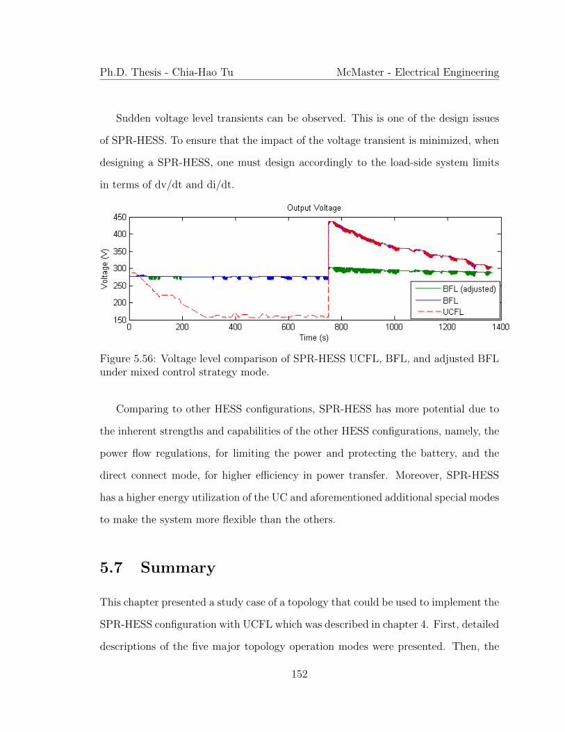
Ph.D. Thesis - Chia-Hao Tu McMaster - Electrical Engineering
Sudden voltage level transients can be observed. This is one of the design issues
of SPR-HESS. To ensure that the impact of the voltage transient is minimized, when
designing a SPR-HESS, one must design accordingly to the load-side system limits
in terms of dv/dt and di/dt.
Figure 5.56: Voltage level comparison of SPR-HESS UCFL, BFL, and adjusted BFLunder mixed control strategy mode.
Comparing to other HESS configurations, SPR-HESS has more potential due to
the inherent strengths and capabilities of the other HESS configurations, namely, the
power flow regulations, for limiting the power and protecting the battery, and the
direct connect mode, for higher efficiency in power transfer. Moreover, SPR-HESS
has a higher energy utilization of the UC and aforementioned additional special modes
to make the system more flexible than the others.
5.7 Summary
This chapter presented a study case of a topology that could be used to implement the
SPR-HESS configuration with UCFL which was described in chapter 4. First, detailed
descriptions of the five major topology operation modes were presented. Then, the
152

Ph.D. Thesis - Chia-Hao Tu McMaster - Electrical Engineering
proposed power management and two control strategies, UC charge sustaining and UC
charge depletion modes, were presented. Detailed analytical models with derivations
of feedback controller transfer functions for of each five different PEC operation modes
then were presented. The simulation parameters, models, and techniques used to
verify the topology operation modes were described. Then, the simulation results of
the PEC functionalities and the SPR-HESS topology used in UDDS drive cycle were
presented and discussed. Lastly, comparative analysis amongst the different HESS
configurations via simulation was discussed in the last section of the chapter.
153

Chapter 6
Experimental Setup and Results
6.1 Introduction
In this chapter, first, the design specifications of the PEC, battery, and UC packs
are presented. Then, the implementation of the experimental setup and results are
discussed. The experiment focuses on verifying the functionalities of the SPR-HESS.
6.2 Experimental Setup Design and Implementa-
tion
6.2.1 Power Electronics Converter
Table 6.1 shows the PEC design parameters in which the PEC is rated at 48V and
500W maximum with switching frequency capability of up to 100kHz. The power in-
ductor has an inductance of 10uH with an internal DC resistance (DCR) of 2.6mOhm
with a maximum of 40% current ripple. The output capacitance of the PEC is selected
154

Ph.D. Thesis - Chia-Hao Tu McMaster - Electrical Engineering
to be 100uF.
Table 6.1: Design parameters of the 500W 48V PEC
Maximum load power 500W
Switching frequency, fs 100kHz
High speed switching devices Infineon IPB036N12N3 G
Power inductor, L 10 uH, DCR=2.6mOhm
Max. inductor current ripple 40%
Co (at the DC link) 100 uF
Figure 6.1a shows the printed circuit board (PCB) design; figure 6.1b is the actual
populated PEC PCB.
155

Ph.D. Thesis - Chia-Hao Tu McMaster - Electrical Engineering
(a) PCB design of PEC
(b) Populated PEC PCB
Figure 6.1: PEC design and implementation.
156

Ph.D. Thesis - Chia-Hao Tu McMaster - Electrical Engineering
6.2.2 Accumulator Selection and Design
For this experimental setup, a lithium polymer battery pack, with 6 series cell in 1
parallel branch (6s1p), is used. As for the UC pack, Maxwell BCAP0100T07 cells
are used; the UC pack is configured to be 12s1p. Table 6.2 and Table 6.3 provide the
battery and UC pack parameters.
Table 6.2: Battery Pack Information
Configuration 6s1p
Voltage Range 16.8V to 25.2V
Nominal Voltage 22.2V
Maximum Power 2.3kW
Capacity 5.2Ah
Table 6.3: UC Pack Information
Configuration 12s1p
Voltage Range @ 65◦C 0V to 32.4V
Voltage Range @ 85◦C 0V to 27.6V
Maximum Power @ 65◦C @ 2700W/kg 0.3564kW
Maximum Power @ 85◦C @ 1900W/kg 0.2508kW
Weight 0.132kg
Volume 0.205L
157
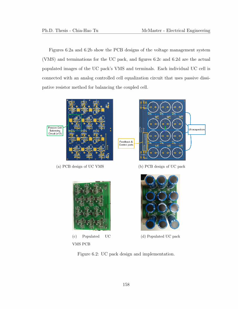
Ph.D. Thesis - Chia-Hao Tu McMaster - Electrical Engineering
Figures 6.2a and 6.2b show the PCB designs of the voltage management system
(VMS) and terminations for the UC pack, and figures 6.2c and 6.2d are the actual
populated images of the UC pack’s VMS and terminals. Each individual UC cell is
connected with an analog controlled cell equalization circuit that uses passive dissi-
pative resistor method for balancing the coupled cell.
(a) PCB design of UC VMS (b) PCB design of UC pack
(c) Populated UC
VMS PCB
(d) Populated UC pack
Figure 6.2: UC pack design and implementation.
158

Ph.D. Thesis - Chia-Hao Tu McMaster - Electrical Engineering
6.3 Experimental Results and Discussion
Figure 6.3: Experimental setup.
Figure 6.3 shows the experimental setup which includes a combined load resistors of
20 Ohm, a SPR-HESS PEC, a micro-controller board, an auxiliary power supply, the
UC pack, and a power supply that emulates the battery pack. The reason of using
a power supply in place of the battery pack is the current-limiting functionality of
the power supply; otherwise, the supplying voltage remains in the same range as the
aforementioned battery pack. For all the experiments conducted, the battery, which
is emulated by the power supply, provides a stable voltage of around 25V. Battery
regenerative operations are not conducted.
159
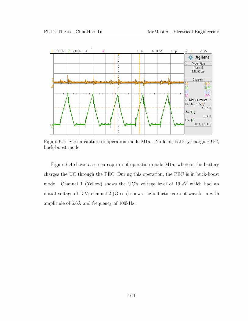
Ph.D. Thesis - Chia-Hao Tu McMaster - Electrical Engineering
Figure 6.4: Screen capture of operation mode M1a - No load, battery charging UC,buck-boost mode.
Figure 6.4 shows a screen capture of operation mode M1a, wherein the battery
charges the UC through the PEC. During this operation, the PEC is in buck-boost
mode. Channel 1 (Yellow) shows the UC’s voltage level of 19.2V which had an
initial voltage of 15V; channel 2 (Green) shows the inductor current waveform with
amplitude of 6.6A and frequency of 100kHz.
160

Ph.D. Thesis - Chia-Hao Tu McMaster - Electrical Engineering
(a) Target voltage of 30V
(b) Target voltage of 35V
Figure 6.5: Screen captures of operation mode M3a-1 - Battery only, boost mode.
Figure 6.5 shows screen captures of operation mode M3a-1, wherein the battery
is the only power supplier to the load and its voltage is boosted. The results of two
161

Ph.D. Thesis - Chia-Hao Tu McMaster - Electrical Engineering
different targeted output voltages of 30V and 35V are shown in figures 6.5a and figure
6.5b, respectively. Channel 1 (Yellow) shows the output voltage waveform of the PEC;
channel 2 (Green) shows the inductor current waveform and its frequency; channel 3
(Blue) shows the battery current with an average of 2.36A for voltage output of 30V
and 3.82A for voltage output of 35V.
Figure 6.6: Screen capture of operation mode M3a-3 - Battery only, direct mode.
Figure 6.6 shows a screen capture of operation mode M3a-3, wherein the battery
is directly connected to the load. As a result, the output voltage is at 23V. The
reason for the output voltage to be slightly lower than the actual battery voltage is
around 2V voltage drop occur on a combination of the current sensing resistor and
the MOSFET’s internal diode.
162

Ph.D. Thesis - Chia-Hao Tu McMaster - Electrical Engineering
(a) Target voltage of 20V
(b) Target voltage of 15V
Figure 6.7: Screen captures of operation mode M3b-1 - Battery only, buck-boostmode.
Figure 6.7 shows screen captures of operation mode M3b-1. Similar to M3a-1
aforementioned, the battery is the only power source to the load, however, the PEC
163

Ph.D. Thesis - Chia-Hao Tu McMaster - Electrical Engineering
is in buck-boost mode. The results of two different targeted output voltages of 20V
and 15V are shown in figures 6.7a and 6.7b, respectively. Channel 1 (Yellow) shows
the output voltage waveform of the PEC; channel 2 (Green) shows the inductor
current waveform and its frequency; channel 3 (Blue) shows the battery current with
an average of 1.7A for voltage output of 20V and 1A for voltage output of 15V.
Figure 6.8 shows screen captures of operation mode M4-1. In this operation mode,
the UC and the battery share the load; the PEC is in buck-boost mode. Figure 6.8a
shows a brief M2 operation when only the UC is connected to the load; channel 1
(Yellow) shows the UC voltage of 16.7V, which is also the output voltage; channel 4
(Red) shows the UC current of 1.21A. Then, the PEC turns on so that the battery
can assist the UC in providing the power to the load as shown in figure 6.8b. As can
be seen in the figure, channel 3 (Blue) shows the battery current with an average of
1.64A; as a result of current sharing, the UC current is reduced from 1.21A to 0.31A.
Similarly, figure 6.9 also shows screen captures of operation mode M4-1. However,
in this case, the UC’s charge is being maintained by the battery; hence, it is in
UC sustaining mode. Figure 6.9a shows a brief M2 operation when only the UC is
connected to the load; channel 1 (Yellow) shows the UC voltage of 16.2V, which is
also the output voltage; channel 4 (Red) shows the UC current of 1.2A. Then, figure
6.9b shows the results of when the battery is connected and provides higher power
than that in the previous case. As a result, UC’s current is greatly reduced and is
able to maintain the initial starting voltage.
164

Ph.D. Thesis - Chia-Hao Tu McMaster - Electrical Engineering
(a)
(b)
Figure 6.8: Screen captures of operation mode M4-1 - Battery // UC, buck-boostmode - Load sharing operation.
165

Ph.D. Thesis - Chia-Hao Tu McMaster - Electrical Engineering
(a)
(b)
Figure 6.9: Screen captures of operation mode M4-1 - Battery // UC, buck-boostmode - UC charge sustaining operation.
166

Ph.D. Thesis - Chia-Hao Tu McMaster - Electrical Engineering
Figure 6.10: Screen capture of operation modes M3a-1 and M5 - Battery only, boostmode and battery + UC, direct series mode.
Figure 6.10 shows the screen capture of about 4.5 seconds of operation; channel
1 (Yellow) shows the final output voltage of the system; channel 3 (Blue) shows the
battery current. The system’s initial operation mode of M3a-3, which is battery only
direct mode, resulting in an output voltage of 23V. Then, it transitions to M3a-1,
battery boost mode, resulting in an output voltage of 30V. Then, the system switches
to the M5 mode where the battery and the UC are connected in series and directly
connected to the load, resulting in an output voltage of 40V.
6.4 Summary
This chapter presented a small-scale experimental setup and experimental results of
the SPR-HESS topology presented. The designs of the power electronic converter,
accumulators, and their parameters were presented in the first section. Then, in the
167

Ph.D. Thesis - Chia-Hao Tu McMaster - Electrical Engineering
second section, several functionalities tests and results were presented to verify the
proposed SPR-HESS topology’s operating theories.
168

Chapter 7
Conclusion
In this dissertation, the safety and performance issues of advanced energy cells, such
as lithium-ion batteries and UC, are introduced first in chapter 2. Management
methods and systems that are used to complement and protect fault-intolerant energy
cells are presented and discussed. There are ways on the higher level of the system to
further complement and improve the management systems aforementioned to boost
the safety and performance of the ESS. Utilizing HESS is one of the methods; the
five fundamental HESS configurations as well as their example topologies studied
by other researchers are presented and discussed in chapter 3. Then, in chapter 4,
the theory of the SPR-HESS configuration is crafted and presented. Its potential
and capabilities are analyzed and compared with other HESS configurations at the
system level point-of-view. Example energy and power management schemes that
can be used to control the SPR-HESS are also presented and later incorporated
in the simulations. Then in chapter 5, a topology that is used to implement the
concepts of SPR-HESS is validated through detailed analysis and simulations; an
extensive comparative analysis amongst all the HESS configurations via simulations
169

Ph.D. Thesis - Chia-Hao Tu McMaster - Electrical Engineering
is conducted. Lastly, in chapter 6, an experimental setup of an SPR-HESS topology
is presented to validate the functionalities.
The results of the simulation comparative analysis show that the cascaded with one
PEC, direct parallel connected, and SPR-HESS configurations are the more promising
configurations amongst the others. In comparison to the SPR-HESS configuration,
the direct parallel connected configuration lacks control and regulation of power flow,
so it needs extra safety design or larger battery pack to protect the battery from
over-discharging/over-charging. The cascaded with one PEC configuration, on the
other hand, has no option of direct connecting the ESSs for high-efficiency operations
or full UC energy utilization.
It is shown that the SPR-HESS adapts and combines the advantages and charac-
teristics of previously proposed HESS configurations proposed by other researchers;
in addition, it introduces flexibilities and new approaches to combining and man-
age ESSs. It is also shown that the SPR-HESS’s UC energy utilization and power
flow efficiency can match that of other configurations and can better utilize the UC
to its fullest to increase the overall energy efficiency of the system in the case of a
battery/UC HESS.
More attention is paid to the ESS side of the system, in this dissertation. There-
fore, future work that is related to this dissertation can be more focused on optimizing
the SPR-HESS and control strategies on the lower level of the system with more con-
siderations of the sizing and scale of the PEC, ESS, cost, and load side electronics,
such as motor inverters, in specific applications of interest. Also, there is an interest
in a comparative study of different topologies that can be used to implement the
SPR-HESS; such potential future work will mostly involve using different isolated
170

Ph.D. Thesis - Chia-Hao Tu McMaster - Electrical Engineering
converter topologies to realize the PEC part of the system.
171

Ph.D. Thesis - Chia-Hao Tu McMaster - Electrical Engineering
172

References
[1] A. Andreiciks, I. Steiks, and O. Krievs, “Current-fed step-up dc/dc converter
for fuel cell applications with active overvoltage clamping,” Scientific Journal of
Riga Technical University, Power and Electrical Engineering, vol. 27, pp. 116–
121, 2010.
[2] A. Andreiciks, I. Steiks, K. Vitols, and L. Ribickis, “Current-fed double inductor
push-pull dc/dc converter with closed loop control system,” in 10th International
Symposium, ”Topical Problems in the Field of Electrical and Power Engineer-
ing”, Jan 2011, pp. 156–160.
[3] F. Azrai, M. Yates, and D. Nelms, “Trench capacitor power supply system
and method,” Sep. 8 2006, wO Patent App. PCT/US2006/002,682. [Online].
Available: https://www.google.ca/patents/WO2006093600A2?cl=en
[4] F. Azrai, M. Yates, and D. Nelms, “Switched-capacitor power supply
system and method,” Mar. 13 2007, uS Patent 7,190,210. [Online]. Available:
https://www.google.ca/patents/US7190210
[5] S. Bergvik and L. Bjorkstrom, “Prolonged useful life and reduced maintenance of
173

Ph.D. Thesis - Chia-Hao Tu McMaster - Electrical Engineering
lead-acid batteries, by means of individual cell voltage regulation,” in Telecom-
munications Energy Conference, 1984. INTELEC ’84. International, Nov 1984,
pp. 63–66.
[6] D. Bjork, “Maintenance of batteries; new trends in batteries and automatic
battery charging,” in Telecommunications Energy Conference, 1986. INTELEC
’86. International, Oct 1986, pp. 355–360.
[7] J. Cao, “Battery/ultra-capacitor hybrid energy storage system for electric, hybrid
electric and plug-in hybrid electric vehicles,” Ph.D. dissertation, Illinois Institute
of Technology, 2010.
[8] J. Cao and A. Emadi, “Batteries need electronics,” IEEE Industrial Electronics
Magazine, vol. 5, no. 1, pp. 27–35, March 2011.
[9] J. Cao and A. Emadi, “A new battery/ultracapacitor hybrid energy storage sys-
tem for electric, hybrid, and plug-in hybrid electric vehicles,” IEEE Transactions
on Power Electronics, vol. 27, no. 1, pp. 122–132, Jan 2012.
[10] J. Cao and A. Emadi, “Hybrid energy storage system,” Oct. 14 2014, uS Patent
8,860,359. [Online]. Available: https://www.google.ca/patents/US8860359
[11] J. Cao, N. Schofield, and A. Emadi, “Battery balancing methods: A comprehen-
sive review,” in IEEE Vehicle Power and Propulsion Conference, 2008. VPPC
’08., Sept 2008, pp. 1–6.
[12] H. Collins, “High power switched capacitor voltage conversion and regu-
lation apparatus,” Dec. 3 1996, uS Patent 5,581,454. [Online]. Available:
https://www.google.ca/patents/US5581454
174

Ph.D. Thesis - Chia-Hao Tu McMaster - Electrical Engineering
[13] W. de Aragao Filho and I. Barbi, “A comparison between two current-fed push-
pull dc-dc converters-analysis, design and experimentation,” in Telecommunica-
tions Energy Conference, 1996. INTELEC ’96., 18th International, Oct 1996,
pp. 313–320.
[14] L. De Sousa, J. Roux, and L. Bendani, “Voltage step-up cir-
cuit,” Dec. 16 2010, uS Patent App. 12/743,266. [Online]. Available:
https://www.google.ca/patents/US20100315048
[15] A. Di Napoli, F. Crescimbini, and L. Solero, “Control strategy for multiple input
dc-dc power converters devoted to hybrid vehicle propulsion systems,” in Pro-
ceedings of the 2002 IEEE International Symposium on Industrial Electronics,
2002. ISIE 2002., vol. 3, 2002, pp. 1036–1041 vol.3.
[16] A. Di Napoli, F. Crescimbini, L. Solero, F. Caricchi, and F. Capponi, “Multiple-
input dc-dc power converter for power-flow management in hybrid vehicles,”
in Industry Applications Conference, 2002. Conference Record of the 37th IAS
Annual Meeting, vol. 3, Oct 2002, pp. 1578–1585 vol.3.
[17] J. Dixon and M. Ortuzar, “Ultracapacitors + dc-dc converters in regenerative
braking system,” Aerospace and Electronic Systems Magazine, IEEE, vol. 17,
no. 8, pp. 16–21, Aug 2002.
[18] X. Fang, N. Kutkut, J. Shen, and I. Batarseh, “Ultracapacitor shift topologies
with high energy utilization and low voltage ripple,” in Telecommunications En-
ergy Conference (INTELEC), 32nd International, June 2010, pp. 1–7.
175

Ph.D. Thesis - Chia-Hao Tu McMaster - Electrical Engineering
[19] H. Fujiwara, “Booster circuit,” Feb. 16 2010, uS Patent 7,663,427. [Online].
Available: https://www.google.ca/patents/US7663427
[20] F. Gagliardi and M. Pagano, “Experimental results of on-board battery-
ultracapacitor system for electric vehicle applications,” in Proceedings of the
2002 IEEE International Symposium on Industrial Electronics, 2002. ISIE 2002.,
vol. 1, 2002, pp. 93–98 vol.1.
[21] T. Gottwald, Z. Ye, and T. Stuart, “Equalization of ev and hev batteries with
a ramp converter,” IEEE Transactions on Aerospace and Electronic Systems,
vol. 33, no. 1, pp. 307–312, Jan 1997.
[22] A. Govindaraj, “Design and characterization of various circuit topologies for
battery/ultracapacitor hybrid energy storage systems,” 2010.
[23] A. Govindaraj, M. King, and S. Lukic, “Performance characterization and opti-
mization of various circuit topologies to combine batteries and ultra-capacitors,”
in IECON 2010 - 36th Annual Conference on IEEE Industrial Electronics Soci-
ety, Nov 2010, pp. 1850–1857.
[24] T. Hanyu, K. Takeda, Y. Kosaka, H. Ooba, and H. Iwano, “Hybrid vehicle
equipped with a variable voltage battery,” Dec. 1 2009, uS Patent 7,626,354.
[Online]. Available: https://www.google.ca/patents/US7626354
[25] S. Hung, D. Hopkins, and C. Mosling, “Extension of battery life via charge
equalization control,” IEEE Transactions on Industrial Electronics, vol. 40, no. 1,
pp. 96–104, Feb 1993.
176
Ph.D. Thesis - Chia-Hao Tu McMaster - Electrical Engineering
[26] K. Iida, T. Hatano, T. Sakuma, and W. Shionoya, “Switching circuit for
generating pulsed power,” Mar. 19 2002, uS Patent 6,359,424. [Online].
Available: https://www.google.ca/patents/US6359424
[27] M. Isaacson, R. Hollandsworth, P. Giampaoli, F. Linkowsky, A. Salim, and V. Te-
ofilo, “Advanced lithium ion battery charger,” in The Fifteenth Annual Battery
Conference on Applications and Advances, 2000., Jan 2000, pp. 193–198.
[28] J. Jackson, “Airworthiness directives; cessna aircraft company airplanes,”
Nov. 1 2011. [Online]. Available: http://www.gpo.gov/fdsys/pkg/FR-2011-11-
01/pdf/2011-27596.pdf
[29] A. Khaligh and Z. Li, “Battery, ultracapacitor, fuel cell, and hybrid energy
storage systems for electric, hybrid electric, fuel cell, and plug-in hybrid electric
vehicles: State of the art,” IEEE Transactions on Vehicular Technology, vol. 59,
no. 6, pp. 2806–2814, July 2010.
[30] H. Kim, “Direct current power apparatus using capaci-
tor,” Apr. 17 2001, uS Patent 6,218,818. [Online]. Available:
https://www.google.ca/patents/US6218818
[31] J. Kimball and P. Krein, “Analysis and design of switched capacitor converters,”
in Twentieth Annual IEEE Applied Power Electronics Conference and Exposi-
tion, 2005. APEC 2005., vol. 3, March 2005, pp. 1473–1477 Vol. 3.
[32] R. King, T. Richter, and L. Salasoo, “Energy storage system for electric
or hybrid vehicle,” Feb. 10 2009, uS Patent 7,489,048. [Online]. Available:
https://www.google.ca/patents/US7489048
177

Ph.D. Thesis - Chia-Hao Tu McMaster - Electrical Engineering
[33] J. Kotowski and W. McIntyre, “Buck and boost switched capacitor gain stage
with optional shared rest state,” Mar. 6 2001, uS Patent 6,198,645. [Online].
Available: https://www.google.ca/patents/US6198645
[34] N. Kutkut and D. Divan, “Dynamic equalization techniques for series battery
stacks,” in 18th International Telecommunications Energy Conference, 1996. IN-
TELEC ’96., Oct 1996, pp. 514–521.
[35] H. Larico and I. Barbi, “Double-coupled current-fed push-pull dc/dc converter:
Analysis and experimentation,” in Power Electronics Conference, 2009. COBEP
’09. Brazilian, Sept 2009, pp. 305–312.
[36] A. Lateef, A. Emadi, and H. Kojori, “Analysis and design of a high voltage
active electric accumulator,” in Transportation Electrification Conference and
Expo (ITEC), 2013 IEEE, June 2013, pp. 1–6.
[37] S. Liu and R. Dougal, “Design and analysis of a current-mode controlled bat-
tery/ultracapacitor hybrid,” in Industry Applications Conference, 2004. Confer-
ence Record of the 2004 IEEE 39th IAS Annual Meeting., vol. 2, Oct 2004, pp.
1140–1145 vol.2.
[38] S. Lu, K. Corzine, and M. Ferdowsi, “High efficiency energy storage system
design for hybrid electric vehicle with motor drive integration,” in Industry Ap-
plications Conference, 2006. 41st IAS Annual Meeting. Conference Record of the
2006 IEEE, vol. 5, Oct 2006, pp. 2560–2567.
[39] S. Lu, K. Corzine, and M. Ferdowsi, “A new method of utilizing ultra-capacitor
energy sources in hybrid electric vehicles over a wide speed range,” in Applied
178

Ph.D. Thesis - Chia-Hao Tu McMaster - Electrical Engineering
Power Electronics Conference, APEC 2007 - Twenty Second Annual IEEE, Feb
2007, pp. 222–228.
[40] S. Lukic, S. Wirasingha, F. Rodriguez, J. Cao, and A. Emadi, “Power manage-
ment of an ultracapacitor/battery hybrid energy storage system in an hev,” in
IEEE Vehicle Power and Propulsion Conference, 2006. VPPC ’06., Sept 2006,
pp. 1–6.
[41] R. Mark, “Ntsb identifies short circuit on 787 battery,” Feb. 11 2013.
[Online]. Available: http://www.ainonline.com/aviation-news/ainsafety/2013-
02-11/ntsb-identifies-short-circuit-787-battery
[42] W. McIntyre and J. Kotowski, “Switched capacitor circuit having voltage
management and method,” Jan. 2 2001, uS Patent 6,169,673. [Online].
Available: https://www.google.ca/patents/US6169673
[43] W. McIntyre and J. Kotowski, “Switched capacitor array circuit for use in dc-dc
converter and method,” May 13 2003, uS Patent 6,563,235. [Online]. Available:
https://www.google.ca/patents/US6563235
[44] A. Melse, “Multi-mode switched capacitor dc-dc voltage con-
verter,” Apr. 12 2011, uS Patent 7,923,865. [Online]. Available:
https://www.google.ca/patents/US7923865
[45] D. Nebrigic, M. Jevtitch, V. Gartstein, W. Milam, J. Sherrill, N. Busko,
and P. Hansen, “Ultra-capacitor based dynamically regulated charge pump
power converter,” Apr. 9 2002, uS Patent 6,370,046. [Online]. Available:
https://www.google.ca/patents/US6370046
179

Ph.D. Thesis - Chia-Hao Tu McMaster - Electrical Engineering
[46] G. Nielson and A. Emadi, “Hybrid energy storage systems for high-performance
hybrid electric vehicles,” in Vehicle Power and Propulsion Conference (VPPC),
2011 IEEE, Sept 2011, pp. 1–6.
[47] K. Nishijima, H. Sakamoto, and K. Harada, “A pwm controlled simple and high
performance battery balancing system,” in IEEE 31st Annual Power Electronics
Specialists Conference, 2000. PESC 00., vol. 1, 2000, pp. 517–520 vol.1.
[48] F. Nome and I. Barbi, “A zvs clamping mode-current-fed push-pull dc-dc con-
verter,” in Industrial Electronics, 1998. Proceedings. ISIE ’98. IEEE Interna-
tional Symposium on, vol. 2, Jul 1998, pp. 617–621 vol.2.
[49] S. Nork, “Inductorless step-up and step-down converter with inrush
current limiting,” Oct. 26 1999, uS Patent 5,973,944. [Online]. Available:
https://www.google.ca/patents/US5973944
[50] T. Ogata and T. Suzuki, “Dc-dc converter with switchable ca-
pacitors,” Dec. 23 2008, uS Patent 7,468,898. [Online]. Available:
https://www.google.ca/patents/US7468898
[51] M. Olszewski, “Evaluation of the 2004 toyota prius hybrid synergy drive system,”
May 2005.
[52] M. Olszewski, “Evaluation of the 2010 toyota prius hybrid synergy drive system,”
Mar 2011.
[53] O. Onar and A. Khaligh, “Dynamic modeling and control of a cascaded active
battery/ultra-capacitor based vehicular power system,” in Vehicle Power and
Propulsion Conference, 2008. VPPC ’08. IEEE, Sept 2008, pp. 1–4.
180

Ph.D. Thesis - Chia-Hao Tu McMaster - Electrical Engineering
[54] O. Onar and A. Khaligh, “A novel integrated magnetic structure based dc/dc
converter for hybrid battery/ultracapacitor energy storage systems,” IEEE
Transactions on Smart Grid, vol. 3, no. 1, pp. 296–307, March 2012.
[55] M. Ortuzar, J. Dixon, and J. Moreno, “Design, construction and performance
of a buck-boost converter for an ultracapacitor-based auxiliary energy system
for electric vehicles,” in The 29th Annual Conference of the IEEE Industrial
Electronics Society, 2003. IECON ’03., vol. 3, Nov 2003, pp. 2889–2894 Vol.3.
[56] U. Oshio, “Dc-dc converter and storage apparatus,” Mar. 11 2003, uS Patent
6,531,792. [Online]. Available: https://www.google.ca/patents/US6531792
[57] C. Pascual and P. Krein, “Switched capacitor system for automatic series battery
equalization,” in Twelfth Annual Applied Power Electronics Conference and Ex-
position, 1997. APEC ’97 Conference Proceedings., vol. 2, Feb 1997, pp. 848–854
vol.2.
[58] T. A. Press, “Boeing 787 dreamliner battery was miswired, japan says,”
Feb. 20 2013. [Online]. Available: http://www.ctvnews.ca/sci-tech/boeing-787-
dreamliner-battery-was-miswired-japan-says-1.1163867
[59] I. Roasto, T. Lehtla, T. Moller, and A. Rosin, “Control of ultracapacitors energy
exchange,” in Power Electronics and Motion Control Conference, 2006. EPE-
PEMC 2006. 12th International, Aug 2006, pp. 1401–1406.
[60] I. Rusan, D. Lazarovich, S. Keshri, S. Dangeti, H. Kojori, and I. Vuk,
“Method of charging and discharging of supercapacitors without the use of
181

Ph.D. Thesis - Chia-Hao Tu McMaster - Electrical Engineering
converters or chargers,” Jul. 6 2010, uS Patent 7,750,606. [Online]. Available:
https://www.google.ca/patents/US7750606
[61] H. Shibata, S. Taniguchi, K. Adachi, K. Yamasaki, G. Ariyoshi, K. Kawata,
K. Nishijima, and K. Harada, “Management of serially-connected battery sys-
tem using multiple switches,” in 4th IEEE International Conference on Power
Electronics and Drive Systems, 2001., vol. 2, Oct 2001, pp. 508–511 vol.2.
[62] L. Shiue, M. Chen, H. Nishikawa, and W. Chen, “Configurable power tank for
power delivery and storage,” Nov. 8 2007, uS Patent App. 11/415,231. [Online].
Available: https://www.google.ca/patents/US20070258188
[63] L. Shiue, M. Chen, H. Nishikawa, and W. Chen, “Configurable
power tank,” Apr. 13 2010, uS Patent 7,696,729. [Online]. Available:
https://www.google.ca/patents/US7696729
[64] L. Shiue and H. Chung, “Power supply apparatus and power sup-
ply method,” Aug. 1 2006, uS Patent 7,085,123. [Online]. Available:
https://www.google.ca/patents/US7085123
[65] L. Shiue, A. Sun, and H. Chung, “High current pulse gen-
erator,” Nov. 18 2003, uS Patent 6,650,091. [Online]. Available:
https://www.google.ca/patents/US6650091
[66] B. Smith, “Chevrolet volt battery incident summary report,” NHTSA, Wash-
ington, DC, Tech. Rep. DOT HS 811 573, Jan 2012.
182
Ph.D. Thesis - Chia-Hao Tu McMaster - Electrical Engineering
[67] L. Solero, A. Lidozzi, and J. Pomilio, “Design of multiple-input power converter
for hybrid vehicles,” in Nineteenth Annual IEEE Applied Power Electronics Con-
ference and Exposition, 2004. APEC ’04., vol. 2, 2004, pp. 1145–1151 vol.2.
[68] A. Staff, “Faa grounds boeing 787 dreamliner for battery problems,” Jan. 17
2013. [Online]. Available: http://www.ainonline.com/aviation-news/2013-01-
16/faa-grounds-boeing-787-dreamliner-battery-problems
[69] A. Stepanov, I. Galkin, and L. Bisenieks, “Implementation of supercapacitors
in uninterruptible power supplies,” in Power Electronics and Applications, 2007
European Conference on, Sept 2007, pp. 1–7.
[70] S. Sugimoto, S. Ogawa, H. Katsukawa, H. Mizutani, and M. Okamura, “A study
of series-parallel changeover circuit of a capacitor bank for an energy storage sys-
tem utilizing electric double-layer capacitors,” Electrical Engineering in Japan,
vol. 145, no. 3, pp. 33–42, Nov 2003.
[71] E. Takahara, H. Sato, and J. Yamada, “Series and parallel connections change
over system for electric double layer capacitors (edlcs) to electric vehicle energy
saving,” in Power Conversion Conference, 2002. PCC-Osaka 2002. Proceedings
of the, vol. 2, 2002, pp. 577–581 vol.2.
[72] M. Tang and T. Stuart, “Selective buck-boost equalizer for series battery packs,”
IEEE Transactions on Aerospace and Electronic Systems, vol. 36, no. 1, pp. 201–
211, Jan 2000.
183

Ph.D. Thesis - Chia-Hao Tu McMaster - Electrical Engineering
[73] P. Toor, A. Emadi, and H. Kojori, “Analysis and design of a low voltage ac-
tive electric accumulator,” in Transportation Electrification Conference and Expo
(ITEC), 2013 IEEE, June 2013, pp. 1–6.
[74] C.-H. Tu and A. Emadi, “A novel series-parallel reconfigurable hybrid energy
storage system for electrified vehicles,” in Transportation Electrification Confer-
ence and Expo (ITEC), 2012 IEEE, June 2012, pp. 1–4.
[75] M. Uno, “Series-parallel reconfiguration technique for supercapacitor energy stor-
age systems,” in TENCON 2009 - 2009 IEEE Region 10 Conference, Jan 2009,
pp. 1–5.
[76] D. Weidenheimer, K. Donegan, and D. Morton, “Electronically reconfig-
urable battery,” Jul. 11 2006, uS Patent 7,075,194. [Online]. Available:
https://www.google.ca/patents/US7075194
[77] D. Weidenheimer, K. Donegan, and D. Morton, “Modular electronically
reconfigurable battery system,” Dec. 27 2011, uS Patent 8,084,887. [Online].
Available: https://www.google.ca/patents/US8084887
[78] J. Weimer, B. Nguyen, M. Kazimierczuk, and B. Jordan, “Super
capacitor charging,” Jun. 22 1999, uS Patent 5,914,542. [Online]. Available:
https://www.google.ca/patents/US5914542
[79] M. Wilk and D. Mazaika, “Dynamically reconfigurable high power energy
storage for hybrid vehicles,” Dec. 2 2010, uS Patent App. 12/475,290. [Online].
Available: https://www.google.ca/patents/US20100305792
184

Ph.D. Thesis - Chia-Hao Tu McMaster - Electrical Engineering
[80] Y.-P. Yang and T.-H. Hu, “A new energy management system of directly-driven
electric vehicle with electronic gearshift and regenerative braking,” in American
Control Conference, 2007. ACC ’07, July 2007, pp. 4419–4424.
[81] Y.-P. Yang and Y.-J. Wang, “Electronic gears for electric vehicles with wheel
motor,” in Industrial Electronics Society, 2005. IECON 2005. 31st Annual Con-
ference of IEEE, Nov 2005, pp. 5 pp.–.
[82] H. Yu, “Switcher for switching capacitors,” Oct. 16 2001, uS Patent 6,304,007.
[Online]. Available: https://www.google.ca/patents/US6304007
[83] J. Zeng, L. Burgyan, and R. Holloway, “Highly efficient step-down/step-up and
step-up/step-down charge pump,” Dec. 2 2003, uS Patent 6,657,875. [Online].
Available: https://www.google.ca/patents/US6657875
[84] J. Zheng, T. Jow, and M. Ding, “Hybrid power sources for pulsed current ap-
plications,” IEEE Transactions on Aerospace and Electronic Systems, vol. 37,
no. 1, pp. 288–292, Jan 2001.
185