a hybrid cascaded multilevel inverter with · pdf fileinternational research journal in...
TRANSCRIPT

INTERNATIONAL RESEARCH JOURNAL IN ADVANCED ENGINEERING AND TECHNOLOGY (IRJAET) E - ISSN: 2454-4752 P - ISSN : 2454-4744 VOL 3 ISSUE 2 (2017) PAGES 1888 - 1900
RECEIVED: 09-03-17 PUBLISHED: 24-03-17. March 24, 2017
1888 ©2017 M.Shobana .al.| http://www.irjaet.com
A HYBRID CASCADED MULTILEVEL INVERTER WITH
PREDICTIVE CAPACITOR VOLTAGE OF REDUCED COMMON
MODE VOLTAGE OPERATION AND INCREASED LINEAR
MODULATION M.Shobana1, D.Ramya2, K.Vijayakumar3, M.Sudhakaran 4
1,2UG Student, Dept. of EEE, Ganadipathy Tulsi’s Jain Engineering College, Vellore, India,
3Assistant Professor, Dept. of EEE, Ganadipathy Tulsi’s Jain Engineering College, Vellore, India, 4Associate Professor, Dept. of EEE, Ganadipathy Tulsi’s Jain Engineering College, Vellore, India.
ABSTRACT
For cascaded multilevel inverter topologies with a single DC supply, closed loop capacitor voltage
control is necessary for proper operation. This paper presents zero and reduced common mode voltage
(CMV) operation of a hybrid cascaded multilevel inverter with predictive capacitor voltage control. Each
phase of the inverter is realized by cascading two 3-level flying capacitor inverters with a half bridge module
in between. For the presented inverter topology, there are redundant switching states for each inverter
voltage levels. By using these switching state redundancies, for every sampling instant, a cost function is
evaluated based on the predicted capacitor voltages for each phase. The switching state which minimizes
cost function is treated as the best and is switched for that sampling instant. The inverter operates with zero
CMV for a modulation index up to 96%. For modulation indices from 96% to 98% the inverter can operate
with reduced CMV magnitude (Vdc/20) and reduced CMV switching frequency using the new space-vector
PWM (SVPWM) presented herein. As a result, the linear modulation range is increased to 98% as compared
to 96% for zero CMV operation. Simulation and experimental results are presented for the inverter topology
for various steady state and transient operating conditions by running an induction motor drive with open
loop V/f control scheme.
Index Terms: Predictive Control, Induction motor drive, PWM, Multilevel inverter, Common mode
voltage, Floating capacitor
1. INTRODUCTION
Multilevel inverters result in reduced voltage harmonic distortion and are ideal for low switching frequency
high performance medium voltage application, commonly used multilevel inverter topologies are Neutral
Point Clamped inverter (NPC), Flying Capacitor inverter (FC). Cascaded H-Bride inverter (CHB) and
hybrid topologies .Hybrid cascaded inverter topologies result in more voltage levels with reduced number of
DC supplies and semiconductor devices compared to NPC, FC and CHB. In recent years, model predictive
control (MPC) has proved to be a good choice for the control of power converter and motor drive
applications. MPC predicts system behavior using a system model and current system state. For multilevel
inverters, which have a finite number of switching states, a predictive controller can select the best state
from a number of possible states.
A cost function is evaluated for each of the finite states and the state which minimizes the cost function is
used for operation. When number of finite states of the system increases, the computation process also

INTERNATIONAL RESEARCH JOURNAL IN ADVANCED ENGINEERING AND TECHNOLOGY (IRJAET) E - ISSN: 2454-4752 P - ISSN : 2454-4744 VOL 3 ISSUE 2 (2017) PAGES 1888 - 1900
RECEIVED: 09-03-17 PUBLISHED: 24-03-17. March 24, 2017
1889 ©2017 M.Shobana .al.| http://www.irjaet.com
increases for predictive control. In high dynamic performance predictive control algorithm with reduced
computations is presented for an asymmetric cascaded H-bridge inverter. a predictive current controller for
cascaded H-bridge inverter with reduced computations is presented. FPGA based implementations of MPC
algorithms for NPC and CHB inverter topologies are presented in and respectively.
Rectifier Inverter
Fig 1. Voltage Source Inverter
Predictive control algorithm is used to minimize the circulating current and balance the DC bus voltage of a
modular multilevel inverter topology. Reduced or zero CMV operation is desirable for voltage source
inverter fed motor drives to avoid motor bearing failure By using a modified PWM switching technique , for
a two level inverter, the effect of CMV and common mode current (motor bearing current) can be reduced.
In multilevel inverter fed motor drive applications, it is possible to make the CMV zero. This is done by
selecting voltage space vectors with zero CMV for synthesizing the reference voltage. The disadvantage of
zero CMV operation is the reduction in linear modulation range compared to that of normal inverter
operation. In a SVPWM technique is presented to extend the linear modulation range of multilevel inverters
with reduced CMV switching. In this paper, a cascaded multilevel inverter with a single DC supply is
operated with zero and reduced common-mode voltage with a predictive capacitor voltage controller.
Floating capacitors are used for generating the multiple voltage levels.
2. INVERTER TOPOLOGY
Fig.2 Hybrid Seven Level Inverter Topology

INTERNATIONAL RESEARCH JOURNAL IN ADVANCED ENGINEERING AND TECHNOLOGY (IRJAET) E - ISSN: 2454-4752 P - ISSN : 2454-4744 VOL 3 ISSUE 2 (2017) PAGES 1888 - 1900
RECEIVED: 09-03-17 PUBLISHED: 24-03-17. March 24, 2017
1890 ©2017 M.Shobana .al.| http://www.irjaet.com
A cost function is evaluated separately for each phase of the inverter to reduce computation time. Also
zero and reduced CMV operation of the inverter with SVPWM technique is analyzed. A new space vector
PWM technique is proposed for the first time with a reduced CMV magnitude (Vdc/20) and reduced CMV
switching frequency (three times the fundamental frequency).Using this technique, 10%increaseinthe linear
modulation range is achieved compared to zero CMV operation, resulting in improved DC bus utilization.
VaOis defined as inverter pole voltage (voltage between inverter pole ‘a’ and DC bus mid point ‘O’), Vanis
defined as motor phase voltage (voltage between inverter pole ‘a’ and DC motor neutral ‘n’ ) and VnOis
defined as common mode voltage (voltage between motor neutral ‘n’ and DC bus mid point ‘O’).Fig. 2
shows the power circuit of a hybrid cascaded multilevel inverter with a single DC supply. The topology
consists of five pairs of complementary switches with 32 (25) switching states for each phase. The switches
Sx1, Sx2, Sx3, Sx4, Sx5 and Sx10, Sx20, Sx30, Sx40, Sx50 respectively (x = a, b, c phases) are operated in
a complementary manner (Sx1 = 1 implies Sx1 is ON and Sx10 is OFF). The three capacitors (Cx1, Cx2 and
Cx3) per phase are maintained at voltages Vdc/2, Vdc/3, and Vdc/6 respectively. Each phase of the topology
can be analysed as a cascaded combination of three-level flying capacitor inverter with a modified fivelevel
flying capacitor inverter. This combination of three level and five level inverters can generate eleven voltage
levels at ‘a’, ‘b’ and ‘c’ with respect to DC bus mid point ‘O’. Seven out of these 11 levels can control
capacitor voltages over a switching cycle irrespective of the load power factor and modulation index. This
feature can be used for reducing the capacitor size for a given power level. For each of these seven levels.
The redundant switching states and effect of these switching states on capacitor charge for a given current
direction for phase ‘a’. It can be noted that for pole voltage levels −Vdc/2 and Vdc/2, all capacitors of that
phase are bypassed and hence the voltages are unaffected. For pole voltage levels −Vdc/3, 0, and Vdc/3,
there are four redundant switching states, and for pole voltage levels−Vdc/6 and Vdc/6, there are five
redundant switching states. For the remaining four pole voltages (−5Vdc/6,−4Vdc/6, 4Vdc/6 and 5Vdc/6),
the capacitor charging depends on both modulation index and load power factor. This imposes operating
limit for the stable operation of inverter and requires special control algorithms to maintain the capacitor
voltage. So these pole voltages are not used for the inverter operation presented in this work. In SVPWM
with hysteresis band based capacitor voltage control schemes, the capacitor voltages are compared to
reference voltages in a hysteresis comparator. At each sampling instant, the controller selects the switching
state from a look-up table based on the hysteresis outputs and desired pole voltage .The controller does not
consider the present value of capacitor voltage and phase current, and capacitor voltages may cross the
hysteresis bands for some load conditions, resulting in higher capacitor voltage ripple. Further, the capacitor
voltage dynamics are sensitive to the static look-up table entries.
3. BLOCK DIAGRAM
It is the first stage of this project. It gives the DC supply to Inverter. It is obtained from an existing power
supply network or from a rotating alternator through a rectifier or a battery, fuel cell, photovoltaic array or
magneto hydrodynamic generator.

INTERNATIONAL RESEARCH JOURNAL IN ADVANCED ENGINEERING AND TECHNOLOGY (IRJAET) E - ISSN: 2454-4752 P - ISSN : 2454-4744 VOL 3 ISSUE 2 (2017) PAGES 1888 - 1900
RECEIVED: 09-03-17 PUBLISHED: 24-03-17. March 24, 2017
1891 ©2017 M.Shobana .al.| http://www.irjaet.com
Fig.3 Block Diagram of Inverter
DC Source Multilevel Inverter
In order to overcome the world excess energy demands,the world trend is replacing the traditional energy
sources(TES) which bassed on non sustainability sources such as fossil fuels and nuclesr fission by utilizing
new efficient and clean energy resources,that are based on natural sources,such as sunlight power ,wind
power and geothermal poweer in addition to ocean energy and bioenergy.All these energy sources decrease
carbon emission,and it classified as renewable energy sources(RES).
Fig.4 Block Diagram for DC Source Multilevel Inverter
4. PREDICTIVE CAPACITOR VOLTAGE CONTROL
In predictive control, capacitor voltages for the next sampling instant are predicted using the
present capacitor voltages, phase currents and inverter switching functions. To control the
dynamics of capacitor voltage, a cost function is evaluated using the predicted capacitor voltages
for every redundant switching state. The switching state which minimizes the cost function is
switched to generate the inverter pole voltage level. A phase shifting transformer with multiple
secondary windings is often utilized mainly for the line current distortions. The rectifier converts

INTERNATIONAL RESEARCH JOURNAL IN ADVANCED ENGINEERING AND TECHNOLOGY (IRJAET) E - ISSN: 2454-4752 P - ISSN : 2454-4744 VOL 3 ISSUE 2 (2017) PAGES 1888 - 1900
RECEIVED: 09-03-17 PUBLISHED: 24-03-17. March 24, 2017
1892 ©2017 M.Shobana .al.| http://www.irjaet.com
the power supply voltage to a dc voltage with a fixed or variable magnitude. The generally used
rectifier topologies include multi-pulse diode or thyristor rectifiers and pulse width modulation
(PWM) rectifiers. The dc link can simply be a capacitor that supplies a stiff dc voltage in voltage-
source inverters or an inductor that smoothes the dc current in current-source inverters.
Fig.5 Typical Block Diagram of Medium Voltage Variable Speed Drives
For current-source drives, two topologies have found industrial applications in high power ranges:
the load-commutated inverter (LCI) and the PWM-CSI. The LCI has been utilized for many years presenting
simple converter topology, low manufacturing cost, and reliable operation. Its main problems include low
input power factor and distorted input current waveforms, which these problems are overcame by the newer
technology of PWM-CSI .
The information about the pole voltage levels to be switched and the time duration of each pole voltage
levels to be applied can be obtained from the SVPWM algorithm. The‘a’,‘b’and‘c’phase timing signals and
the pole voltage transitions over a switching cycle ‘Ts’. In general, with SVPWM, the inverter pole voltage
of xth phase remains at level ‘lx+1’ for a duration of ‘Tx’ and at ‘lx’ for a duration of ‘Ts-Tx’. Using
capacitor voltages Vcxk(n) and phase current ix measured at nth sampling instant along with the pole
voltage level data and timing information, the capacitor voltage for the duration ‘Tx’ can be predicted as,
Vcxk = Vcxk(n+1) − Vcxkref (1)
where V cxkref is the reference voltage of kth capacitor of xth phase. The predictive capacitor voltage
control uses a cost function. For zero CMV and reduced CMV operation, the cost function for each phase is
evaluated separately. For each phase, by using a separate cost function, phase capacitors are controlled
independently and ensures best switching state is selected for each phase. With individual cost function for
each phase, the number of computation required also reduces. The number of computation required with
single cost function will be (redundancy of ‘a’ × redundancy of ‘a’ × redundancy of ‘c’) compared to
(redundancy of ‘a’ + redundancy of ‘b’ + redundancy of ‘c’) with individual cost function. The cost function
for each switching state, the optimal switching state for the pole voltage level ‘lx+1’ can be obtained and all
the capacitor voltages can be predicted for the duration ‘Tx’. Using this information, optimal switching state
for the pole voltage level ‘lx’ for the duration ‘Ts-Tx’ also can be obtained.
For nth sampling instant, using level shifted carrier based SVPWM, get the xth phase pole voltage
level and timing information for inverter operation. 2) Predict (n+1)th instant capacitor voltage using
SVPWM data, previous capacitor voltages and load current. 3) Evaluate the cost function gx for all the

INTERNATIONAL RESEARCH JOURNAL IN ADVANCED ENGINEERING AND TECHNOLOGY (IRJAET) E - ISSN: 2454-4752 P - ISSN : 2454-4744 VOL 3 ISSUE 2 (2017) PAGES 1888 - 1900
RECEIVED: 09-03-17 PUBLISHED: 24-03-17. March 24, 2017
1893 ©2017 M.Shobana .al.| http://www.irjaet.com
possible switching states for the level data ‘lx+1’ and ‘lx’. Find the switching state which minimizes the cost
function gx for each phase. 4) Apply the switching state for each phase and repeat the process from step 1
for next sampling instant. Fig. 3 shows the convergence of cost function over time, during motor start-up
with all capacitors for phase ‘a’ initially at 0V. The voltage build-up of capacitors from a relaxed state of 0V
for predictive control and hysteresis control it can be seen that the steady state condition (i.e all capacitors
are charged to reference) is reached faster with predictive controller than with a hysteresis controller.
5. NINE LEVEL INVERTER SPACE VECTOR STRUCTURE AND ZERO CMV LOCATIONS
A seven level inverter has 343 (73) pole voltage combinations which are mapped to 127 space vector
locations in the α−β plane. Out of these pole voltage combinations, 37 pole voltage combinations have zero
common mode voltage with respect to motor neutral ‘n’ and DC bus midpoint ‘O’ (VnO = (VaO + VbO +
VcO)/3). Combining these zero CMV space vector locations, a four level inverter space vector structure
rotated 300 anticlockwise is obtained as shown in the Fig. 5. The reference vector (−−→ Vref) is synthesized
by averaging three adjacent vectors using (7 and 8). Analysing the zero CMV space vector structure,
maximum peak of fundamental voltage possible is 0.499Vdc compared to 0.577Vdc with normal seven level
inverter operation (for 0.577Vdc, m = 1 and 0.499Vdc, m = 0.86).
6. REDUCED CMV OPERATION TO EXTEND LINEAR MODULATION RANGE
As mentioned in the previous section, with zero CMV operation, DC bus utilization of the inverter gets
reduced. In order to get the same torque capability for the induction motor operated with a normal seven
level inverter, the DC link voltage needs to be increased for zero CMV operation. Instead of this, by
allowing reduced common mode switching, DC bus utilization of inverter is improved compared to zero
CMV operation. For the seven level inverter the next CMV near to zero is ±Vdc/20. For reduced CMV
operation presented in this paper, space vector triangles overlap in some regions. This conflict is solved by
using the following method.
Fig.6 Space vector structure showing reduced CMV

INTERNATIONAL RESEARCH JOURNAL IN ADVANCED ENGINEERING AND TECHNOLOGY (IRJAET) E - ISSN: 2454-4752 P - ISSN : 2454-4744 VOL 3 ISSUE 2 (2017) PAGES 1888 - 1900
RECEIVED: 09-03-17 PUBLISHED: 24-03-17. March 24, 2017
1894 ©2017 M.Shobana .al.| http://www.irjaet.com
7. SIMULATION AND EXPERIMENTAL AND RESULTS
The inverter topology with predictive control is simulated in MATLAB-SIMULINK by modelling the
inverter using switching functions. Induction motor is modelled with respect to stator axis reference frame.
Various modulation techniques for multilevel power converters are presented. For zero CMV operation (m
≤ 0.866) presented here, a level shifted carrier based PWM algorithm is used to get the space vector
locations and PWM timings. For reduced CMV operation, PWM timings and space vector locations to be
switched are obtained using a triangle search algorithm. This algorithm searches one by one all the triangles
formed by nearest space vector locations in a sector for positive values of dwell times T0, T1 and T2.
The operation of inverter with predictive capacitor voltage control is tested on a 3 phase induction motor
drive with open loop V/f control scheme. Synchronous PWM technique is used for testing the inverter
topology. Number of samples per sector is taken as 12 for fundamental frequency ranging from 15 Hz to 25
Hz, 9 for 25 Hz to 37.5 Hz, and 6 for 37.5 Hz to 45 Hz. For fundamental frequency below 15 Hz inverter is
operated with a constant switching frequency of 900 Hz. Simulation results under various operating
conditions are presented. The zero CMV steady state operation of inverter for fundamental frequencies 10
Hz and 40 Hz the performance of predictive capacitor voltage controller over a hysteresis band based
capacitor voltage controller in terms of voltage ripple during no load and full load for fundamental
frequencies 10 Hz and 40 Hz with same SVPWM technique.
The frequency spectrum of inverter pole voltage VaO for reduced CMV operation and normal seven level
inverter operation. A 3 phase, 400V, 3.7kW, 50 Hz, 4 pole induction motor drive with open loop V/f control
scheme is implemented in hardware for testing the proposed topology. TMS320F28335 DSP is used as the
main controller and Xilinx SPARTAN-3 XC3S200 FPGA as the PWM signal generator with a dead time of
2.5 µs
Fig 7. Multilevel inverter for Each Phase

INTERNATIONAL RESEARCH JOURNAL IN ADVANCED ENGINEERING AND TECHNOLOGY (IRJAET) E - ISSN: 2454-4752 P - ISSN : 2454-4744 VOL 3 ISSUE 2 (2017) PAGES 1888 - 1900
RECEIVED: 09-03-17 PUBLISHED: 24-03-17. March 24, 2017
1895 ©2017 M.Shobana .al.| http://www.irjaet.com
Fig.8 Circuit Design of Pulse with Modulation
The maximum voltage that appears across the load resistor is nearly-but never exceeds-500 v0lts, as
result of the small voltage drop across the diode. In the bridge rectifier shown in view B, the maximum
voltage that can be rectified is the full secondary voltage, which is 1000 volts. Therefore, the peak output
voltage across the load resistor is nearly 1000 volts. With both circuits using the same transformer, the
bridge rectifier circuit produces a higher output voltage than the conventional full-wave rectifier circuit.
Fig.9 Voltage waveform
INTERNATIONAL RESEARCH JOURNAL IN ADVANCED ENGINEERING AND TECHNOLOGY (IRJAET) E - ISSN: 2454-4752 P - ISSN : 2454-4744 VOL 3 ISSUE 2 (2017) PAGES 1888 - 1900
RECEIVED: 09-03-17 PUBLISHED: 24-03-17. March 24, 2017
1896 ©2017 M.Shobana .al.| http://www.irjaet.com
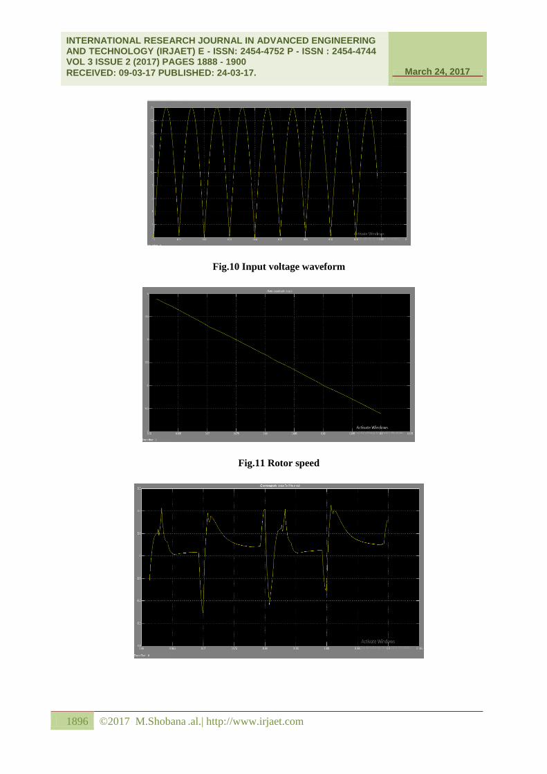
Fig.10 Input voltage waveform
Fig.11 Rotor speed
INTERNATIONAL RESEARCH JOURNAL IN ADVANCED ENGINEERING AND TECHNOLOGY (IRJAET) E - ISSN: 2454-4752 P - ISSN : 2454-4744 VOL 3 ISSUE 2 (2017) PAGES 1888 - 1900
RECEIVED: 09-03-17 PUBLISHED: 24-03-17. March 24, 2017
1897 ©2017 M.Shobana .al.| http://www.irjaet.com
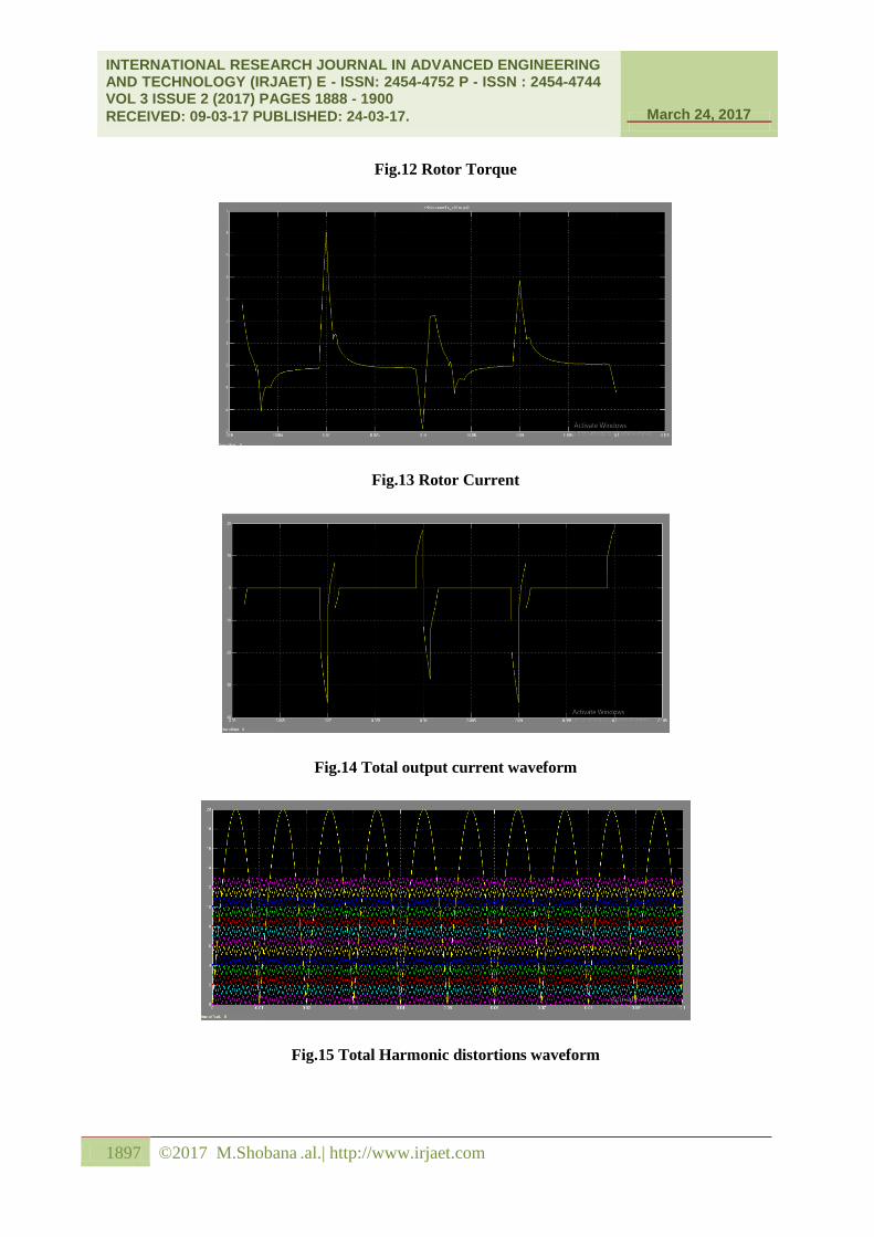
Fig.12 Rotor Torque
Fig.13 Rotor Current
Fig.14 Total output current waveform
Fig.15 Total Harmonic distortions waveform

INTERNATIONAL RESEARCH JOURNAL IN ADVANCED ENGINEERING AND TECHNOLOGY (IRJAET) E - ISSN: 2454-4752 P - ISSN : 2454-4744 VOL 3 ISSUE 2 (2017) PAGES 1888 - 1900
RECEIVED: 09-03-17 PUBLISHED: 24-03-17. March 24, 2017
1898 ©2017 M.Shobana .al.| http://www.irjaet.com
Fig.16 SPWM filtered line voltage
Fig.17 Cascaded Multilevel Inverter
CONCLUSION
The hybrid PWM techniques for one level inverter are proposed in this project. The proposed space vector
hybrid PWM leads to lowest distortion in its class of PWM at any given modulation index for a given
average switching frequency. The hybrid PWM is compared to the sinusoidal PWM technique. The results
of SPWM are compared with SVPWM. The proposed techniques lead to about reduction in line current
distortion over SPWM at the rated voltage and rated frequency of the drive. The superior performance of the
proposed techniques over SPWM and existing PWM techniques has been demonstrated using simulation.
Hybrid PWM will be further carried out in aim of reducing THD and hardware of the system will be done to
verify the simulation results in real time.
REFERENCES
[1] S. Kouro, M. Malinowski, K. Gopakumar, J. Pou, L. G. Franquelo, B. Wu, J. Rodriguez, M. A. Perez,
and J. I. Leon, “Recent advances and industrial applications of multilevel converters,” IEEE Trans. Ind.
Electron, vol. 57, no. 8, pp. 2553–2580, Aug 2010.

INTERNATIONAL RESEARCH JOURNAL IN ADVANCED ENGINEERING AND TECHNOLOGY (IRJAET) E - ISSN: 2454-4752 P - ISSN : 2454-4744 VOL 3 ISSUE 2 (2017) PAGES 1888 - 1900
RECEIVED: 09-03-17 PUBLISHED: 24-03-17. March 24, 2017
1899 ©2017 M.Shobana .al.| http://www.irjaet.com
[2] H. Abu-Rub, J. Holtz, J. Rodriguez, and G. Baoming, “Medium-voltage multilevel converters-state of
the art, challenges, and requirements in industrial applications,” IEEE Trans. Ind. Electron, vol. 57, no. 8,
pp. 2581–2596, Aug 2010.
[3] J. D. Barros, J. F. A. Silva, and . G. A. Jesus, “Fast-predictive optimal control of npc multilevel
converters,” IEEE Trans. Ind. Electron, vol. 60, no. 2, pp. 619–627, Feb 2013.
[4] J. Amini, “An effortless space-vector-based modulation for n -level flying capacitor multilevel inverter
with capacitor voltage balancing capability,” IEEE Trans. Power Electron, vol. 29, no. 11, pp. 6188–6195,
Nov 2014.
[5] S. Thielemans, T. J. Vyncke, and J. Melkebeek, “Weight factor selection for model-based predictive
control of a four-level flying-capacitor inverter,” IET Power Electronics, vol. 5, no. 3, pp. 323–333, March
2012.
[6] S. Choi and M. Saeedifard, “Capacitor voltage balancing of flying capacitor multilevel converters by
space vector pwm,” IEEE Trans. Power Delivery, vol. 27, no. 3, pp. 1154–1161, July 2012.
[7] M. A. Perez, P. Cortes, and J. Rodriguez, “Predictive control algorithm technique for multilevel
asymmetric cascaded h-bridge inverters,” IEEE Trans. Ind. Electron, vol. 55, no. 12, pp. 4354–4361, Dec
2008.
[8] P. Cortes, A. Wilson, S. Kouro, J. Rodriguez, and H. Abu-Rub, “Model predictive control of multilevel
cascaded h-bridge inverters,” IEEE Trans. Ind. Electron, vol. 57, no. 8, pp. 2691–2699, Aug 2010.
[9] T. Geyer and S. Mastellone, “Model predictive direct torque control of a five-level anpc converter drive
system,” IEEE Trans. Ind. Appl, vol. 48, no. 5, pp. 1565–1575, Sept 2012.
[10] P. R. Kumar, P. P. Rajeevan, K. Mathew, K. Gopakumar, J. I. Leon, and L. G. Franquelo, “A three-
level common-mode voltage eliminated inverter with single dc supply using flying capacitor inverter and
cascaded h-bridge,” IEEE Trans. Power Electron, vol. 29, no. 3, pp. 1402–1409, March 2014.
[11] A. K. Gupta and A. M. Khambadkone, “A space vector modulation scheme to reduce common mode
voltage for cascaded multilevel inverters,” IEEE Trans. Power Electron, vol. 22, no. 5, pp. 1672–1681, Sept
2007.
[12] M. Malinowski, K. Gopakumar, J. Rodriguez, and M. A. Perez, “A survey on cascaded multilevel
inverters,” IEEE Trans. Ind. Electron, vol. 57, no. 7, pp. 2197–2206, July 2010.
[13] M. Saeedifard, P. M. Barbosa, and P. K. Steimer, “Operation and control of a hybrid seven-level
converter,” IEEE Trans. Power Electron, vol. 27, no. 2, pp. 652–660, Feb 2012.
[14] P. Cortes, M. P. Kazmierkowski, R. M. Kennel, D. E. Quevedo, and J. Rodriguez, “Predictive control in
power electronics and drives,” IEEE Trans. Ind. Electron, vol. 55, no. 12, pp. 4312–4324, Dec 2008. [15] P.
M. Sanchez, O. Machado, E. J. B. Pea, F. J. Rodrguez, and F. J. Meca, “Fpga-based implementation of a
predictive current controller for power converters,” IEEE Trans. Ind. Info, vol. 9, no. 3, pp. 1312–1321, Aug
2013.
[16] R. O. Ramirez, J. R. Espinoza, P. E. Melin, M. E. Reyes, E. E. Espinosa, C. Silva, and E. Maurelia,
“Predictive controller for a three-phase/singlephase voltage source converter cell,” IEEE Trans. Ind. Info,
vol. 10, no. 3, pp. 1878–1889, Aug 2014
[17] M. A. Perez, J. Rodriguez, E. J. Fuentes, and F. Kammerer, “Predictive control of ac-ac modular
multilevel converters,” IEEE Trans. Ind. Electron, vol. 59, no. 7, pp. 2832–2839, July 2012.
[18] S. Chen, T. A. Lipo, and D. Fitzgerald, “Source of induction motor
bearingcurrentscausedbypwminverters,”IEEETrans.EnergyConvers, vol. 11, no. 1, pp. 25–32, Mar 1996.

INTERNATIONAL RESEARCH JOURNAL IN ADVANCED ENGINEERING AND TECHNOLOGY (IRJAET) E - ISSN: 2454-4752 P - ISSN : 2454-4744 VOL 3 ISSUE 2 (2017) PAGES 1888 - 1900
RECEIVED: 09-03-17 PUBLISHED: 24-03-17. March 24, 2017
1900 ©2017 M.Shobana .al.| http://www.irjaet.com
[19] D. Busse, J. Erdman, R. J. Kerkman, D. Schlegel, and G. Skibinski, “Bearing currents and their
relationship to pwm drives,” IEEE Trans. Power Electron, vol. 12, no. 2, pp. 243–252, Mar 1997.
[20] M. Cacciato, S. Caro, G. Scarcella, G. Scelba, and A. Testa, “Improved space-vector modulation
technique for common mode currents reduction,” IET Power Electronics, vol. 6, no. 7, pp. 1248–1256,
August 2013.