a high voltage ratio and low stress dc-dc converter with...
TRANSCRIPT

lable at ScienceDirect
Renewable Energy xxx (2014) 1e9
Contents lists avai
Renewable Energy
journal homepage: www.elsevier .com/locate/renene
A high voltage ratio and low stress DCeDC converter with reducedinput current ripple for fuel cell source
Mustafa A. Al-Saffar*, Esam H. IsmailElectrical Engineering Department, College of Technological Studies, P.O. Box 35007, Al-Shaab, 36051, Kuwait
a r t i c l e i n f o
Article history:Received 21 May 2014Accepted 7 August 2014Available online xxx
Keywords:Single-switch DCeDC convertersHigh step-up convertersSelf-left SEPIC convertersBoost convertersNon-isolated converters
* Corresponding author. Tel.: þ965 99762279; fax:E-mail addresses: [email protected], alsaffar.musta
[email protected] (E.H. Ismail).
http://dx.doi.org/10.1016/j.renene.2014.08.0200960-1481/© 2014 Elsevier Ltd. All rights reserved.
Please cite this article in press as: Al-Saffarripple for fuel cell source, Renewable Energ
a b s t r a c t
A new single-switch non-isolated dcedc converter with high-voltage gain and reduced semiconductorvoltage stress is proposed in this paper. The proposed topology is derived from the conventional boostconverter integrated with self-lift Sepic converter for providing high voltage gain without extremeswitch duty-cycle. The reduced voltage stress across the power switch enables the use of a lower voltageand RDS-ON MOSFET switch, which will further reduce the conduction losses. Moreover, the low voltagestress across the diodes allows the use of Schottky rectifiers for alleviating the reverse-recovery currentproblem, leading to a further reduction in the switching and conduction losses. Furthermore, the “near-zero” ripple current can be achieved at the input side of the converter which will help improve the fuelcell stack life cycle. The principle of operation, and theoretical are performed. Experimental results of a100 W/240 Vdc output with 24 Vdc input voltage are provided to evaluate the performance of the pro-posed scheme.
© 2014 Elsevier Ltd. All rights reserved.
1. Introduction
Energy shortage and environmental pollution issues haveaccelerated the use of clean energy resources such as wind [1], fuelcell stacks and photovoltaic (PV) [2] power systems. However, theserenewable energy sources or systems have relatively low voltageoutput characteristics and demand high step-up voltage gain andhigh efficiency DCeDC converters, for any potential practicalapplication.
In addition, in grid-connected fuel-cell systems the currentdrawn by the fuel-cell stack has a low-frequency (LF) ripple com-ponents (e.g., 100 Hz or 120 Hz for single-phase systems) and ahigh-frequency (HF) switching ripple components. The LF ripplecomponents is the main factor responsible for low performanceregarding FC energy efficiency and lifetime [3]. It also decreases FCcapacity and increases fuel consumption [4,5]. Adding more inputcapacitors or adding an external active filter is a typical method todepress LF ripple currents at the expense of size and cost penalty.Low frequency ripple cancellation techniques based on feed for-ward and active ripple compensation techniques can be considered
þ965 [email protected] (M.A. Al-Saffar),
MA, Ismail EH, A high voltagy (2014), http://dx.doi.org/10
as an alternative solution [4,6]. In [7], active ripple mitigation basedon nonlinear control has been presented. On the other hand, the HFcurrent ripples componentmay not directly affect the fuel cell stackperformance; however it may affects the characteristics of the fuelcell resulting in lower durability of the fuel cell [8]. Also, the HFcurrent ripples forces the total current to exceed the maximumcurrent rating and this could affect the cycle life of the fuel-cellstack and other components in the system such as the storagebattery. Lessening of the HF current ripple components by utilizingextra filters increases cost and system size. A topological mecha-nism that mitigates both LF and HF current ripples of the FC stackcurrent was proposed in [9]. In general, the overall energy effi-ciency of the fuel-cell power system can be maximized by miti-gating both LF and HF ripples of the stack current.
Practically, the conventional boost converter cannot provide avoltage gain greater than six times its applied voltage due toparasitic components [10]. Moreover, operating the conventionalboost converter with extreme duty-cycle degrades the overallconversion efficiency due to the output diode reverse-recoveryproblems, which will increase the electromagnetic interference(EMI) levels. Also, the conventional boost converter requires a highcurrent and voltage rated MOSFET; hence, it will require a MOSFETwith a higher RDS-ON, which leads to high conduction and switchinglosses [11]. Furthermore, the conventional boost converter requiresa bulky input filter to reduce the large input current ripple. The
e ratio and low stress DCeDC converter with reduced input current.1016/j.renene.2014.08.020

M.A. Al-Saffar, E.H. Ismail / Renewable Energy xxx (2014) 1e92
large input current ripple component may shorten the lifetime ofthe sources as well as decrease the performance of the overallsystem [12].
In an effort to maximize the efficiency and the voltage gain ofDCeDC converter, considerable research efforts have been directedtowards the development of efficient high step-up converters.Interleaving two boost converters can significantly minimize boththe input current ripple and switching losses and double thetransferable power. Interleaving technique has been applied in avariety of applications such as PFC rectification [13] and dcedcconverters [14]. However; besides the complex control, the voltagestress across the semiconductor devices is similar to the conven-tional boost converter. Therefore, the conversion efficiency islimited in high-output voltage applications. Cascading two boostconverters can increase the voltage gain at the expense ofincreasing cost and complex control circuitry [15]. Also, cascadingboost converters is not suitable for high-output-voltage applica-tions due to the high reverse recovery energy losses in the outputdiode.
The problem of the complex control in the cascade boost con-verter can be alleviated by integrating the two switches into oneswitch known as quadratic converter [16]. The characteristics ofquadratic converters and their potential industrial applications arepresented in [17]. A complete efficiency analysis of the quadraticboost converter operating with a sliding-mode-based control sys-tem is presented in detail in [18]. A quadratic converter with zero-current and zero voltage switching (ZC-ZVS) performance isintroduced in [19]. However, the switch voltage stress in thequadratic converter is equal to the output voltage. Thus, noadvantage over the conventional boost converter is achieved. Also,the switch is subjected to high current stress which increases theconduction losses and degrades the overall conversion efficiency.
Converters utilizing coupled inductors can provide high step-upvoltage gain at the expense of degrading system efficiency due tothe losses associated with the leakage inductance [20]. Utilizingactive clamp circuit can recycle the leakage energy [21], but in-creases the cost and complexity of the converter. However, besidestheir pulsating input current, they require high voltage rated powerswitch due to the presence of a resonant circuit between theleakage inductance of the coupled inductor and the parasiticcapacitor of the output diode. In addition, as the turn ratio of thecoupled inductor is increased to extend the voltage gain, the inputcurrent ripple becomes larger and the requirement of insertinginput filter becomes necessary [22]. Besides, the design of the high-frequency components such as the coupled inductors and theresonant elements for these converters is rather complex comparedto the classical boost converter.
Other topologies based on integrated boost converter by aflyback converter can achieve a high-voltage conversion ratio andreduced switch voltage stress. In [23], the boost inductor and thetransformer of the flyback converter are integrated into a singlecoupled inductor. As a result, a high voltage gain can be obtaineddue to the series connection of the outputs of the boost and theflyback converters. Schemes base on integrating a switched-capacitor circuit with a coupled inductor can recycle the energystored in the leakage inductor energy of the coupled-inductor,hence reducing the voltage stress on the power [24]. The voltagegain can be further extended by increasing number of capacitor-diode voltage multiplier cells [25] which increases the overallsystem cost. The proposed topology in [26] further improves thevoltage gain and reduces switch voltage stress over other single-switch high gain converters. However, besides the floatingoutput, it requires additional semiconductor devices which re-duces the overall efficiency and increases the size as well as cost ofthe converter. In addition, the proposed topologies in [23e26]
Please cite this article in press as: Al-Saffar MA, Ismail EH, A high voltagripple for fuel cell source, Renewable Energy (2014), http://dx.doi.org/10
suffer from EMI noise problems due to pulsating input currentripple, thereby requiring a large input filter to be used. The highinput current ripple can be reduced by combining the coupledinductor and voltage doubler cell structure at the expense of uti-lizing two switches which complicate the control of the converter[27].
In this paper, a single-switch non-isolated dcedc converter isproposed to fulfill high step-up requirements [28]. The proposedconverter structure utilizes two inductors which are oftendescribed as a disadvantage. However, the two inductors can bemagnetically coupled into a single magnetic core and near ‘zero-ripple-current’ can be reached at the input port of the converterwithout compromising the performance. In addition, the voltagestress across the active power switch is reduced which enables theuse of MOSFETs with a lower voltage rating and low RDS-ON. Thus,the conversion efficiency can be improved due to the reducedconduction and switching losses. Similarly, the reduced voltagestress across all the diodes in the circuit allows the use of Schottkyrectifiers for alleviating the reverse-recovery current problem,leading to a further reduction in the switching and conductionlosses.
This paper is organized as follows: Sec. 2 presents the proposedcircuit configuration and operating principle in continuous con-duction mode (CCM) and discontinuous inductor conductionmode (DICM). Circuit analysis with coupled inductors is intro-duced in Sec. 3. Sec. 4 gives a design guideline and presents anillustrative example along with simulation verification. Theexperimental results of a 100 W, 24 V-input/240 V-output proto-type with 50 kHz switching frequency are given in Sec. 5 to verifythe analysis. Finally, the conclusions drawn from this study ispresented in Sec. 6.
2. The proposed high step-up converter: principle ofoperation and analysis
Fig. 1 shows three dcedc converters suitable for high step-upapplications [29e31]. The voltage conversion ratio for the con-verters of Fig. 1 is quite high and is twice as large as the step-upratio of the conventional boost converter. This is a very desirablefeature for low-voltage energy sources such as fuel cells (FC) orphotovoltaic cells. However, for FC-based power systems, it ex-pected from the dcedc converter to have a low input current rippleas a high current ripple may reduce the lifetime of the FC. There-fore, the converters of Fig. 1 require a large input inductor (L1) valuein order to reduce the input current ripple within a certain range.Consequently, this increases the total converter size, cost, andreduces the overall power efficiency. Note that the high inputinductance requirement can be reduced by increasing the switch-ing frequency, but this will increase the semiconductor switchinglosses. Furthermore, the voltage stress across the power switchesQ1 and Q2 for the converter of Fig. 1(c) is equal to the output voltageVo. As a result, the conversion efficiency is not high for high outputvoltage applications.
On the contrary, Fig. 2 shows the proposed high step-up con-verter with an extended step-up voltage capability and with “nearzero” input current features. The proposed topology is derivedfrom the conventional boost converter integrated with self-liftSepic converter [32] for providing high voltage gain withoutextreme switch duty-cycle. The proposed converter utilize a singlenon-floating power switch (Q); hence enabling easy driver circuit.However, it should be mentioned here that the proposed topologydoes not have the capability of limiting large current flowingthrough inductor L1 and the diodes in case of overloaded opera-tion. In other words, the proposed topology has the same majorpractical drawbacks as the conventional boost converter, such that
e ratio and low stress DCeDC converter with reduced input current.1016/j.renene.2014.08.020

Fig. 3. Topological stages in CCM for the converter of Fig. 2 a) Switch ON topology, b)switch OFF topology.
Fig. 1. High step-up dcedc converters: (a) Boost converter with one multiplier cell[29], (b) Hybrid switched-capacitor converter [Fig. 2(c) [30]], (c) Charge pump withboost converter [31].
M.A. Al-Saffar, E.H. Ismail / Renewable Energy xxx (2014) 1e9 3
inputeoutput isolation cannot be easily implemented, highstartup inrush current, as well as a lack of current limiting duringoverload conditions.
2.1. Continuous conduction mode (CCM)
Referring to Fig. 2, when the converter operates in CCM, thecurrent ripples through the input inductor L1 can be assumednegligible. In order to simplify the converter analysis, thefollowing assumptions are made during one switching cycle (Ts):1) The input voltage is pure dc, 2) All components are ideal, thusthe efficiency is 100%, and 3) All capacitors are sized to have arelatively small voltage ripple at the switching frequency. Underthese assumptions, the circuit operation in one switching cycle canbe divided into two stages as shown in Figs. 3(a) and (b), whereas
Fig. 2. The proposed high step-up non-isolated dcedc converters.
Please cite this article in press as: Al-Saffar MA, Ismail EH, A high voltagripple for fuel cell source, Renewable Energy (2014), http://dx.doi.org/10
Fig. 4 shows its ideal key waveforms. The operational mode isdescribed briefly next.
Stage 1 [t0, t1], Fig. 3(a): When the power switch Q is turned on,diode D2 is turned on simultaneously. Diodes D1 and D3 are turnedoff by the negative voltage e VC1 and (VC1 e Vo) across them,respectively. In this stage, the currents through the two inductorsincrease linearly at a rate proportional to the input voltage Vg.Capacitor C1 charges capacitor C2 while capacitor C3 is beingcharged by diode D2 current (iC2 e iL2). Referring to Fig. 3(a), notethat the voltage across the capacitor C1 is equal to the sum of thevoltages across both C2 and C3, i.e.,
VC1 ¼ VC2 þ VC3 (1)
At the end of this interval, the switch is turned-off initiating thenext subinterval.
Stage 2 [t1, Ts], Fig. 3(b): At the instant t1, switch Q is turned off,both diodes D1 and D3 are turned on simultaneously providing apath for the input and output inductor currents. Diode D2 is reversebiased by the voltage (VC1e Vo). In this stage, the inductors currentsiL1 and iL2 decreases linearly at a rate proportional to the voltage (Vge VC1). Capacitor C1 is being charged by the current (iC2 þ iL1 e iL2)
Fig. 4. Key waveforms for the proposed converter of Fig. 2 in CCM.
e ratio and low stress DCeDC converter with reduced input current.1016/j.renene.2014.08.020
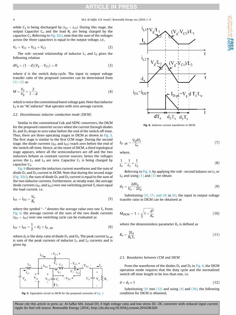
Fig. 6. Inductor current waveforms in DICM.
M.A. Al-Saffar, E.H. Ismail / Renewable Energy xxx (2014) 1e94
while C2 is being discharged by (iL2 þ iC3). During this stage, theoutput Capacitor Co and the load RL are being charged by thecapacitor C3. Referring to Fig. 3(b), note that the sum of the voltagesacross the three capacitors is equal to the output voltage, i.e.,
Vo ¼ VC1 þ VC2 þ VC3 (2)
The voltesecond relationship of inductor L1 and L2 gives thefollowing relation
dVg þ�1� d
��Vg � VC1
� ¼ 0 (3)
where d is the switch duty-cycle. The input to output voltagetransfer ratio of the proposed converter can be determined from(1)e(3) as
M ¼ Vo
Vg¼ 2
1� d(4)
which is twice the conventional boost voltagegain.Note that inductorL2 is an “AC inductor” that operates with zero average current.
2.2. Discontinuous inductor conduction mode (DICM)
Similar to the conventional Cuk and SEPIC converters, the DICMfor the proposed converter occurs when the current through diodesD1 and D3 drops to zero value before the end of the switch off-time.Thus, there are three operating stages in DICM as shown in Fig. 5.The first stage is similar to the first CCM stage. During the secondstage, the diode currents (iD1 and iD3) reach zero before the end ofthe switch off-time. Hence, at the onset of DICM, a third topologicalstage appears, where all the semiconductors are off and the twoinductors behave as constant current sources; hence the voltagesacross the L1 and L2 are zero. Capacitor C1 is being charged bycapacitor C2.
Fig. 6 illustrates the inductors current waveforms and the sum ofdiode D1 and D3 current in DCIM. Note that during the second stage(Fig. 3(b)), the sum of diode D1 and D3 current is equal to the sum ofthe two inductor currents. Furthermore, at steady state, the averagediode currents (iD1 and iD3) over one switching period Ts must equalthe load current, i.e.
iD1 ¼ iD3 ¼ Vo
RL(5)
where the symbol “�” denotes the average value over one Ts. FromFig. 6, the average current of the sum of the two diode currents(iD1 þ iD3) over one switching cycle can be evaluated as
iD1 þ iD3 ¼ 12� d2 � ID�pk (6)
where d2 is the duty-ratio of diode D1 and D3. The peak current ID-pkis sum of the peak currents of inductor L1 and L2 currents and isgiven by,
Fig. 5. Equivalent circuit in DICM for the proposed converter of Fig. 2.
Please cite this article in press as: Al-Saffar MA, Ismail EH, A high voltagripple for fuel cell source, Renewable Energy (2014), http://dx.doi.org/10
ID�pk ¼ VgdTsLe
(7)
where,
1Le
¼ 1L1
þ 1L2
(8)
Referring to Fig. 6, by applying the voltesecond balance on L1 orL2 and using (1) and (3) we obtain
d2 ¼ 2dVg
Vo � 2Vg(9)
Substituting (5), (7), and (9) in (6), the input to output voltagetransfer ratio in DICM can be obtained as
MDICM ¼ 1þffiffiffiffiffiffiffiffiffiffiffiffiffiffi1þ d2
Ke
s(10)
where the dimensionless parameter Ke is defined as
Ke ¼ 2LeRLTs
(11)
2.3. Boundaries between CCM and DICM
From the waveforms of the diodes D1 and D3 in Fig. 6, the DICMoperation mode requires that the duty cycle and the normalizedswitch off-time length to be less than one, i.e.
dþ d2 <1 (12)
Substituting (9) into (12) and using (4) and (10), the followingcondition for DICM is obtained,
e ratio and low stress DCeDC converter with reduced input current.1016/j.renene.2014.08.020

Table 1Component stresses for the converter of Fig. 2.
Circuit parameter Normalized peak voltage Normalized rms current
Switch Q 12
MffiffiffiffiffiffiffiffiffiffiffiffiffiffiffiMðM�2Þ
pDiode D1 and D3
12
1ffiffiffiffiffiffi2M
p
Diode D212
1ffiffiffiffiffiffiffiffiffiffiffiffiffiffiffiMðM�2Þ
pInductor L1 e
ffiffiffiffiffiffiffiffiffiffiffiffiffiffiffiffiffiffiffiffiffiffiffiffiffiffiffiffiffiffiffiffiffiffiffiffiffiffi1þ 1
12
�ðM�2ÞRL
M3L1 fs
�2s
Inductor L2 e ðM�2ÞRL
2ffiffiffi3
pM3L2 fs
Capacitor C1, C2,and C3
MC1 ¼ 12
MC2 ¼ M � 22M
MC3 ¼ 1M
1ffiffiffiffiffiffiffiffiffiffiffiffiffi2ðM�2Þ
p
Capacitor Co 1 1M �
ffiffiffiffiffiffiffiffiffiM�22
q
Fig. 7. The proposed converter with coupled inductors.
M.A. Al-Saffar, E.H. Ismail / Renewable Energy xxx (2014) 1e9 5
Ke <Ke�crit ¼dð1� dÞ2
4¼ M � 2
M3 (13)
Thus, for values of Ke > Ke-crit, the converter operates in CCM;otherwise, the converter operates in DICM. The maximum value ofKe-crit is 1/27 at d ¼ 1/3 where the voltage gain MDICM is equal to 3.
2.4. Component stresses
Table 1 shows the component normalized peak voltage and rmscurrent stresses for the proposed converter of Fig. 2 in CCM. Volt-ages and currents are normalizedwith respect to the output voltageVo and the average input current IL1, respectively. These equationsare given for design purposes.
Referring to Table 1, it is clear that the voltage stress across thesemiconductor devices is equal to half of the output voltage Vo. Onthe other hand, the switch is subjected to a relatively higher rmscurrent stress since it must supply current to two inductors and acapacitor. This is the main disadvantage of the proposed converter.However, the low switch voltage stress enables the use of a lowervoltage rated with low RDS�ON which greatly reduces switch con-duction losses.
3. The proposed converter with coupled inductors
Referring to Fig. 4, the voltage waveforms across the two in-ductors L1 and L2 are identical. Thus, the two inductors can bemagnetically coupled into a single magnetic core as shown in Fig. 7.Accordingly, the converter size, weight, and cost are reduced.Moreover, by proper selection of the coupling coefficients (k12),‘near-zero current ripples’ at the input inductor L1 can be achievedwithout compromising performance. This condition is very desir-able, because the generated EMI noise is minimized and welldramatically reduces input filtering requirements. For FC poweredsystems, the reduced converter input high frequency current ripplecan prevent high frequency interaction inside the FC stack and mayextend the fuel cell lifetime cycle. Also, the circuit of Fig. 7 can drawfree ripple current in the input port not only in CCM as well inDICM, where the high switching ripple is of concern. This is a veryattractive feature for power factor correction applications since itwill minimize the EMI effect and the input filtering stage. In reality,the ripple current is not exactly reduced to zero but is highlyreduced. The reason for this is due to integer number of turns, andthe voltages across the inductors are not exactly identical due to
Please cite this article in press as: Al-Saffar MA, Ismail EH, A high voltagripple for fuel cell source, Renewable Energy (2014), http://dx.doi.org/10
inductor equivalent series resistance (ESR) and the ripple voltageacross the individual capacitors.
Referring to Fig. 7, the rate of change of the inductor currents iL1and iL2 during switch on-time is given by,
2664diL1dtdiL2dt
3775 ¼ 1
L1L2 �M212
�L2 �M12
�M12 L1
��VgVC3
�(14)
where
M12 ¼ k12ffiffiffiffiffiffiffiffiffiffiL1L2
p(15)
is the mutual inductance of the windings. At a steady-state,VC3 ¼ Vg, then from (14) the following conditions must be satis-fied for zero ripple in the input inductor L1
diL1dt
¼ VgðL2 �M12ÞL1L2 �M2
12
¼ 0 (16)
Eq. (16) implies that the ripple at the input inductor can besteered toward L2 if the following condition is satisfied:
M12 ¼ L20k12 ¼ffiffiffiffiffiL2L1
s<1 (17)
During switch Q off-time, the conditions for zero ripple in theinput inductor is similar to that of (17). It is important to mentionhere that the voltage gain for the proposed converter is indepen-dent of the magnetic coupling coefficient k12. In other words, theDC voltage gain in (4) is valid whether using two separate inductors(2 cores) or two coupled inductors (single core). It should be alsomentioned here that the ‘near-zero ripples’ in input current featurecan also be obtained in the conventional Cuk and Sepic converterusing coupled inductors [33,34]. However, the proposed converterhas an advantage of a higher voltage gain, reduced switch anddiode voltage stresses. It should be mentioned here that a coupledSepic converter with reduce switch voltage stress has been pro-posed in [35]. However, the proposed converter in this study hashigher voltage gain and lower voltage stress compared to the one in[35].
The steady-state analysis presented in Sec. 2 for the uncoupledinductors is also valid for the coupled-inductor extension, exceptfor the definition of the effective inductance Le (8). This is becauseonly inductor L2 determines the switching current ripple. Thus, forthe coupled-inductor case, the definition of Le becomes Le ¼ L2.
Thus, the minimum required value for L2 which ensure CCMoperation can be found from (11) and (13) and it is given by
e ratio and low stress DCeDC converter with reduced input current.1016/j.renene.2014.08.020

M.A. Al-Saffar, E.H. Ismail / Renewable Energy xxx (2014) 1e96
L2 >ðM � 2ÞRLTs
2M3 (18)
Once the value of L2 is selected, the value of L1 can be calculatedfrom (17).
Selection of the capacitors is generally selected to limit voltageripple to the level required by the specification. Referring to Fig. 4,the peak-to-peak voltage ripple across the various capacitors in theproposed converter can be determined as
DvCn ¼ Vo
RLCnfs; n ¼ 1; 2; 3 (19)
whereas the peak-to-peak voltage ripple across the output filtercapacitor Co is given by
DvCo ¼ VodRLCofs
(20)
Also, selection of capacitors C1, C2 and C3 must ensure that theconverter does not operate discontinuous-capacitor-voltage-mode(DCVM). Therefore, the resonant frequencies of (L1, C1), (L2, C2)and (L2, C3) should be lower than the switching frequency fs toassure the capacitor voltages VC1, VC2, and VC3 to be constant in aswitching period.
4. Design procedure and simulation
A step-by-step design procedure is presented in this section, andan example of how to determine the component values of theproposed converter of Fig. 2 is given.
4.1. Design guidelines
To illustrate the design procedure, the converter of Fig. 2 isdesigned with the following specifications:
� Input voltage Vg ¼ 24 V;� Output voltage Vo ¼ 240 V;� Output power Pout ¼ 100 W;� Switching frequency fs ¼ 50 kHz;� Maximum peak input current ripple DiL1 ¼ 30% of IL1;� Output voltage ripple Dvo < ± 0.05% of Vo.
From the specifications above, the voltage conversion ratio gainis M ¼ 10. Assuming the efficiency is 100%, the values of the circuitcomponents are calculated as follows:
a) Switch duty cycle d: from (4), the required switch duty cycle d isfound as
d ¼ M � 2M
¼ 0:8 (21)
b) To achieve the input current ripple requirement, the inputinductance value L1 must be
L1 � V2g d
2� 15%� fs � Pin¼ 307:2 mH (22)
c) The value of the critical conduction parameter Ke-crit can beevaluated from (10), and it is given by
Please cite this article in press as: Al-Saffar MA, Ismail EH, A high voltagripple for fuel cell source, Renewable Energy (2014), http://dx.doi.org/10
Ke�crit ¼M � 2M3 ¼ 0:008 (23)
From (11) and (23), the minimum value of the equivalentinductance Le required for CCM operation is
Le�crit ¼Ke�critRL
2fs¼ 46:1 mH (24)
For CCM operation, the value of Le must be greater than Le-crit. Inthis example, we set L1 ¼ L2 ¼ 180 mH. In this case, evaluating (8)gives Le ¼ 90 mH which is five times greater than Le-crit. Note that,according to the selected value of L1, the percentage of the peakcurrent ripple in L1 is
%DiL1 ¼ Vgd2L1fsIL1
� 100 ¼ 25:6% (25)
d) The required output capacitance Co to maintain peakepeakoutput voltage ripple of 0.1% of Vo can be calculated from (20)as
Co >Vod
RLDvCofs¼ 27:8 mF (26)
4.2. Simulation verification
The proposed converter of Fig. 2 has been simulated by PSpicecircuit simulator to verify the above design parameters as well as tomeasure its performance in terms of efficiency. For the simulation,Pspice actual semiconductor models have been used to simulatethe switches; STPS10150CT Schottky rectifier (150 V, 5 A,VF ¼ 0.75 V) for the diodes, and IRF6641PBF (200 V, 4.6 A, RDS-ON¼ 51mU) for the power MOSFET switch Q. The capacitors' valuesare set to 47 mF. Furthermore, an ESR of 20mU is connected in serieswith each capacitor and inductor to model its losses.
Fig. 8 shows the simulated waveforms for the converter of Fig. 2in CCM. Diode D3 voltage waveform is not shown since it is similarto diode D1 voltagewaveform. Fig. 8(a) shows that the input currentripple is about 25% as predicted by (25). Fig. 8(b), (c), and (d) showsthat the voltage stresses of the power switch Q and diodes D1 andD2 are half of the output voltage Vo. Fig. 8(b) also shows that theswitch turn-on current spike is reduced mainly due to the smallpeak reverse-recovery currents of D1 and D3. The voltage wave-forms of capacitors C1, C2, and C3 are shown in Fig. 8(e) with goodagreement with theoretical predictions shown in Table 1. Thesimulated results correctly demonstrate the CCM operating modewith a simulated conversion efficiency of 97.5%.
In order to demonstrate the effect of coupling the inductors onthe input line current, the circuit of Fig. 7 has been simulated withcoupled inductors. The circuit parameters were all the same asthose for the uncoupled case except for the value of L2. The value ofthe coupling coefficients k12 is set to 0.83. Hence, according to (17),the value of L2 is 125 mH. The simulated inductors current wave-forms are shown in Fig. 9, where the high-frequency switchingripples' magnitude in the input current iL1 is greatly reduced due tothe coupling of the two inductors. Consequently, the generated EMInoise level is greatly minimized as well as the requirement for theinput filtering.
4.3. Averaged circuit model
The averaged model for the proposed converter of Fig. 2 isderived here based on averaging switches waveforms during one
e ratio and low stress DCeDC converter with reduced input current.1016/j.renene.2014.08.020
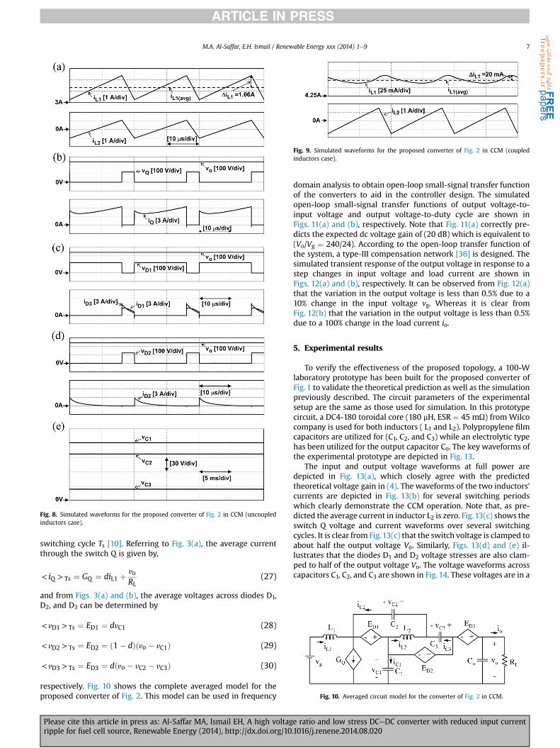
Fig. 9. Simulated waveforms for the proposed converter of Fig. 2 in CCM (coupledinductors case).
Fig. 10. Averaged circuit model for the converter of Fig. 2 in CCM.
Fig. 8. Simulated waveforms for the proposed converter of Fig. 2 in CCM (uncoupledinductors case).
M.A. Al-Saffar, E.H. Ismail / Renewable Energy xxx (2014) 1e9 7
switching cycle Ts [10]. Referring to Fig. 3(a), the average currentthrough the switch Q is given by,
< iQ > Ts ¼ GQ ¼ diL1 þvoRL
(27)
and from Figs. 3(a) and (b), the average voltages across diodes D1,D2, and D3 can be determined by
< vD1 > Ts ¼ ED1 ¼ dvC1 (28)
< vD2 > Ts ¼ ED2 ¼ ð1� dÞðvo � vC1Þ (29)
< vD3 > Ts ¼ ED3 ¼ dðvo � vC2 � vC3Þ (30)
respectively. Fig. 10 shows the complete averaged model for theproposed converter of Fig. 2. This model can be used in frequency
Please cite this article in press as: Al-Saffar MA, Ismail EH, A high voltagripple for fuel cell source, Renewable Energy (2014), http://dx.doi.org/10
domain analysis to obtain open-loop small-signal transfer functionof the converters to aid in the controller design. The simulatedopen-loop small-signal transfer functions of output voltage-to-input voltage and output voltage-to-duty cycle are shown inFigs. 11(a) and (b), respectively. Note that Fig. 11(a) correctly pre-dicts the expected dc voltage gain of (20 dB) which is equivalent to(Vo/Vg ¼ 240/24). According to the open-loop transfer function ofthe system, a type-III compensation network [36] is designed. Thesimulated transient response of the output voltage in response to astep changes in input voltage and load current are shown inFigs. 12(a) and (b), respectively. It can be observed from Fig. 12(a)that the variation in the output voltage is less than 0.5% due to a10% change in the input voltage vg. Whereas it is clear fromFig. 12(b) that the variation in the output voltage is less than 0.5%due to a 100% change in the load current io.
5. Experimental results
To verify the effectiveness of the proposed topology, a 100-Wlaboratory prototype has been built for the proposed converter ofFig. 1 to validate the theoretical prediction as well as the simulationpreviously described. The circuit parameters of the experimentalsetup are the same as those used for simulation. In this prototypecircuit, a DC4-180 toroidal core (180 mH, ESR ¼ 45 mU) from Wilcocompany is used for both inductors ( L1 and L2). Polypropylene filmcapacitors are utilized for (C1, C2, and C3) while an electrolytic typehas been utilized for the output capacitor Co. The key waveforms ofthe experimental prototype are depicted in Fig. 13.
The input and output voltage waveforms at full power aredepicted in Fig. 13(a), which closely agree with the predictedtheoretical voltage gain in (4). The waveforms of the two inductors'currents are depicted in Fig. 13(b) for several switching periodswhich clearly demonstrate the CCM operation. Note that, as pre-dicted the average current in inductor L2 is zero. Fig.13(c) shows theswitch Q voltage and current waveforms over several switchingcycles. It is clear from Fig.13(c) that the switch voltage is clamped toabout half the output voltage Vo. Similarly, Figs. 13(d) and (e) il-lustrates that the diodes D1 and D2 voltage stresses are also clam-ped to half of the output voltage Vo. The voltage waveforms acrosscapacitors C1, C2, and C3 are shown in Fig. 14. These voltages are in a
e ratio and low stress DCeDC converter with reduced input current.1016/j.renene.2014.08.020

Fig. 11. Simulated open-loop small-signal frequency responses. (a) Output voltage-to-input voltage. (b) Output voltage-to-duty cycle control signal.
M.A. Al-Saffar, E.H. Ismail / Renewable Energy xxx (2014) 1e98
good agreement with theoretical predictions shown in Table 1 andwith the simulated voltages in Fig. 8(e). The measured powerconversion efficiency is about 95.8%. It should be mentioned thatthe experimental results are obtained in the absence of any snubbercircuits and without any special circuit layout. Therefore, it is ex-pected that higher efficiency can be achieved by improving thelayout and utilizing better components.
6. Conclusion
In this paper, a new high voltage gain single-switch DCeDCconverter is proposed. The proposed topology is suitable for several
Fig. 12. Closed-loop step responses for the converter in Fig. 2 with a type-IIIcompensation network. (a) Due to a step change in input voltage vg. (b) Due to astep change in load current io.
Fig. 13. Measured waveforms for the proposed converter of Fig. 2.
Please cite this article in press as: Al-Saffar MA, Ismail EH, A high voltage ratio and low stress DCeDC converter with reduced input currentripple for fuel cell source, Renewable Energy (2014), http://dx.doi.org/10.1016/j.renene.2014.08.020

Fig. 14. Measured capacitors voltage waveforms for the proposed converter of Fig. 2.
M.A. Al-Saffar, E.H. Ismail / Renewable Energy xxx (2014) 1e9 9
applications such as fuel cell, photovoltaic, and UPS systems, wherehigh voltage gain between the input and output voltages aredemanded. The proposed converter is regulated by the conven-tional PWM technique at constant frequency. The proposed con-verters can achieve a high step-up conversion ratio withoututilizing a line- or high-frequency step-up transformer and alsomaintain low voltage stress across all semiconductors. The reducedvoltage stress across the controlled switch allows utilization ofMOSFET with reduced on-resistance. Features of the proposedconverters and their operating principles have been discussed inthis paper. The steady-state behavior has been studied andanalyzed with performance characteristics, and a large-signal-averaged model is presented. The input current ripple can besignificantly reduced to near-zero level by coupling the inductorswhich also increases the power density of the converter and im-proves the durability for the fuel cell.
The performance of the proposed converter is further investi-gated under conditions of load current and input voltage changesbased on the average model. The simulation and experimental re-sults proved the validity of theoretical analysis and the feasibility ofthe proposed converter. Finally, the proposed converter can beconsidered a competitive alternative for practical applicationswhere a high-voltage transfer gain is demanded, such as renewableenergy systems, with simple structure and high efficiency.
References
[1] Kesraoui M, Korichi N, Belkadi A. Maximum power point tracker of windenergy conversion system. Renew Energy 2011;36:2655e62.
[2] Shuhui L, Timothy AH, Dawen L, Fei H. Integrating photovoltaic and powerconverter characteristics for energy extraction study of solar PV systems.Renew Energy 2011;36:3238e45.
[3] Thounthong P, Davat B, Ra€el S, Sethakul P. Fuel cell high-power applications.IEEE Ind Electron Mag 2009;3(1):32e46.
[4] Liu C, Lai JS. Low frequency current ripple reduction technique with activecontrol in a fuel cell power system with inverter load. IEEE Trans PowerElectron 2007;22(4):1429e36.
[5] Fontes G, Turpin C, Saisset R, Meynard T, Astier S. Interactions between fuelcells and power converters influence of current harmonics on a fuel cell stack.In: Proc. IEEE Power Electronics Specialists Conf. Aachen, Germany; 2004.p. 4729e35.
[6] WaiRJ, LinCY.Dual active low-frequency ripple control for clean-energypower-conditioning mechanism. IEEE Trans Ind Electron 2011;58(11):5172e85.
[7] Bizon N. A new topology of fuel cell hybrid power source for efficient oper-ation and high reliability. J Power Sources 2011;196(6):3260e70.
Please cite this article in press as: Al-Saffar MA, Ismail EH, A high voltagripple for fuel cell source, Renewable Energy (2014), http://dx.doi.org/10
[8] Wang H, Ren Z, Park JD. Power electronic converters for microbial fuel cellenergy extraction: effects of inductance, duty ratio, and switching frequency.J Power Sources 2012;220(15):89e94.
[9] Mazumder SK, Burra RK, Acharya KA. Ripple-mitigating and Energy-Efficientfuel cell power-conditioning system. IEEE Trans Power Electron 2007;22(4):1437e52.
[10] Erickson RW, Maksimovic D. Fundamentals of power electronics. 2nd ed. NewYork: Kluwer; 2001.
[11] Li W, He X. Review of nonisolated high-step-up DC/DC converters in photo-voltaic grid-connected applications. IEEE Trans Power Electron 2011;58(4):1239e50.
[12] Gerard M, Poirot-Crouvezier J, Hissel D, P�era M. Ripple current effects onPEMFC aging test by experimental and modeling. J Fuel Cell Sci Technol2010;8(2):021004e5.
[13] Miwa BA, Otten DM, Schlecht MF. High efficiency power factor correctionusing interleaving technique. In: IEEE Pro. APEC'921; 1992. p. 557e68.
[14] Huang X, Wang Xi, Nergaard T, Lai J-S, Xu X, Zhu L. parasitic ringing anddesign issues of digitally controlled high power interleaved boost converters.IEEE Trans Power Electron 2004;19(5):1341e52.
[15] Haroun R, Cid-Pastor A, El Aroudi A, Martınez-Salamero L. Synthesis of ca-nonical elements for power processing in DC distribution systems usingcascaded converters and sliding-mode control. IEEE Trans Power Electron2014;29(3):1366e81.
[16] Maksimovic D, Cuk S. Switching converters with wide DC conversion range.IEEE Trans Power Electron 1991;6(1):151e7.
[17] Wijeratne DS, Moschopoulos G. Quadratic power conversion for power elec-tronics: principles and circuits. IEEE Trans Circuits Syst-I 2012;59(2):426e38.
[18] Lopez-Santos O, Martinez-Salamero L, Garcia G, Valderrama-Blavi H,Mercuri DO. Efficiency analysis of a sliding-mode controlled quadratic boostconverter. IET Power Electron 2013;6(2):364e73.
[19] Al-Saffar MA, Ismail EH, Sabzali AJ. Family of ZC-ZVS converters with widevoltage range for renewable energy systems. Renew Energy 2013;56:32e43.
[20] Ma KW, Lee YS. An integrated flyback converter for dc uninterruptible powersupply. IEEE Trans Power Electron 1996;11(2):318e27.
[21] Zhao Q, Lee FC. High-efficiency, high step-up DC-DC converters. IEEE TransPower Electron 2003;18(1):65e73.
[22] Wu TF, Lai YS, Hung JC, Chen YM. Boost converter with coupled inductors andbuckeboost type of active clamp. IEEE Trans Ind Electron 2008;55(1):154e62.
[23] Tseng KC, Liang TJ. Novel high-efficiency step-up converter. IEE Proc ElectrPower Appl 2004;151(2):182e90.
[24] Wai RJ, Duan RY. High-efficiency dc/dc converter with high voltage gain. IEEProc Electr Power Appl 2005;152(4):793e802.
[25] Liang TJ, Chen SM, Yang LS, Chen JF, Ioinovici A. Ultra-large gain step-upswitched-capacitor DC-DC converter with coupled inductor for alternativesources of Energy. IEEE Trans Circuit Syst-I: Reg Paper 2012;59(4):864e74.
[26] Fardoun AA, Ismail EH. Ultra step-up DC-DC converter with reduced switchstress. IEEE Trans Ind Appl 2010;46(5):2025e34.
[27] Zhao Y, Li W, He X. Single-phase improved active clamp coupled-inductor-based converter with extended voltage doubler cell. IEEE Trans Power Elec-tron 2012;27(6):2869e78.
[28] Al-Saffar MA. High voltage gain DCeDC converter with low input currentripple for fuel cell source. In: ICREGA'14-Renewable Energy: Generation andApplications Conf. Springer Proceedings in Energy; 2014. p. 179e92. http://dx.doi.org/10.1007/978-3-319-05708-8_14.
[29] Prudente M, Pfitscher LL, Emmendoerfer G, Romaneli EF, Gules R. Voltagemultiplier cells applied to non-isolated DC-DC converters. IEEE Trans PowerElectron 2008;23(2):871e87.
[30] Ismail EH, Al-Saffar MA, Sabzali AJ. High conversion ratio DC-DC converterswith reduced switch stress. IEEE Trans Circuit Syst-I: Reg Paper 2008;55(7):2139e51.
[31] Hwu KI, Yau YT. High step-up converter based on charge pump and boostconverter. IEEE Trans Power Electron 2012;27(5):2484e94.
[32] Zhu M, Luo FL. Series SEPIC implementing voltage-lift technique for DCeDCpower conversion. IET Power Electron 2008;1(1):109e21.
[33] Cuk S, Middlebrook RD. Advances in switched-mode power conversion Part II.IEEE Trans Ind Electron 1983;30(1):19e29.
[34] Ismail EH, Fardoun AA, Zerai AA. Step-up/step-down DC-DC converter withnear zero input/output current ripples. Int J Circ Theor Appl 2014;42(4):358e75.
[35] Fardoun AA, Ismail EH, Sabzali AJ, Al-Saffar MA. Bidirectional converter forhigh-efficiency fuel cell powertrain. J Power Sources 2014;249:470e82.
[36] Venable HD. The K factor: a new mathematical tool for stability analysis andsynthesis. Proc Powercon 1983:1e12. H-1.
e ratio and low stress DCeDC converter with reduced input current.1016/j.renene.2014.08.020