a heuristic method for statistical digital circuit sizingboyd/papers/pdf/stat_design_ml06_talk.pdfa...
TRANSCRIPT

A Heuristic Method for Statistical Digital
Circuit Sizing
Stephen Boyd Seung-Jean Kim Dinesh PatilMark Horowitz
Microlithography’06 2/23/06

Statistical variation in digital circuits
• growing in importance as devices shrink
• modeling still open
– many sources: environmental, process parameter variation,lithography
– intrachip, interchip variation– distributions, correlations not well known, change as process matures
Microlithography’06 2/23/06 1

Statistical digital circuit sizing
• standard design approaches: margining, guardbanding, design overcorners
• statistical design explicitly takes statistical variation into account(combines circuit design with design for manufacturing, yieldoptimization, design centering, . . . )
• statistical design is very hard problem (even for small circuits)
• this talk: a (relatively) simple heuristic method for statistical designthat appears to work well
Microlithography’06 2/23/06 2

Outline
• A quick example
• Digital circuit sizing: models and optimization
• New method for statistical digital circuit sizing
• Digital circuit sizing example
• Conclusions and future work
Microlithography’06 2/23/06 3

A Quick Example

Example: Ladner-Fisher 32-bit adder
• 64 inputs, 33 outputs, 451 gates, 3214 paths, max depth 8
• simplified RC delay model
• design variables: 451 scale factors for gates
• cycle time Tcycle is max path delay
• minimize cycle time subject to limits on area, min/max scale factor
Microlithography’06 2/23/06 4
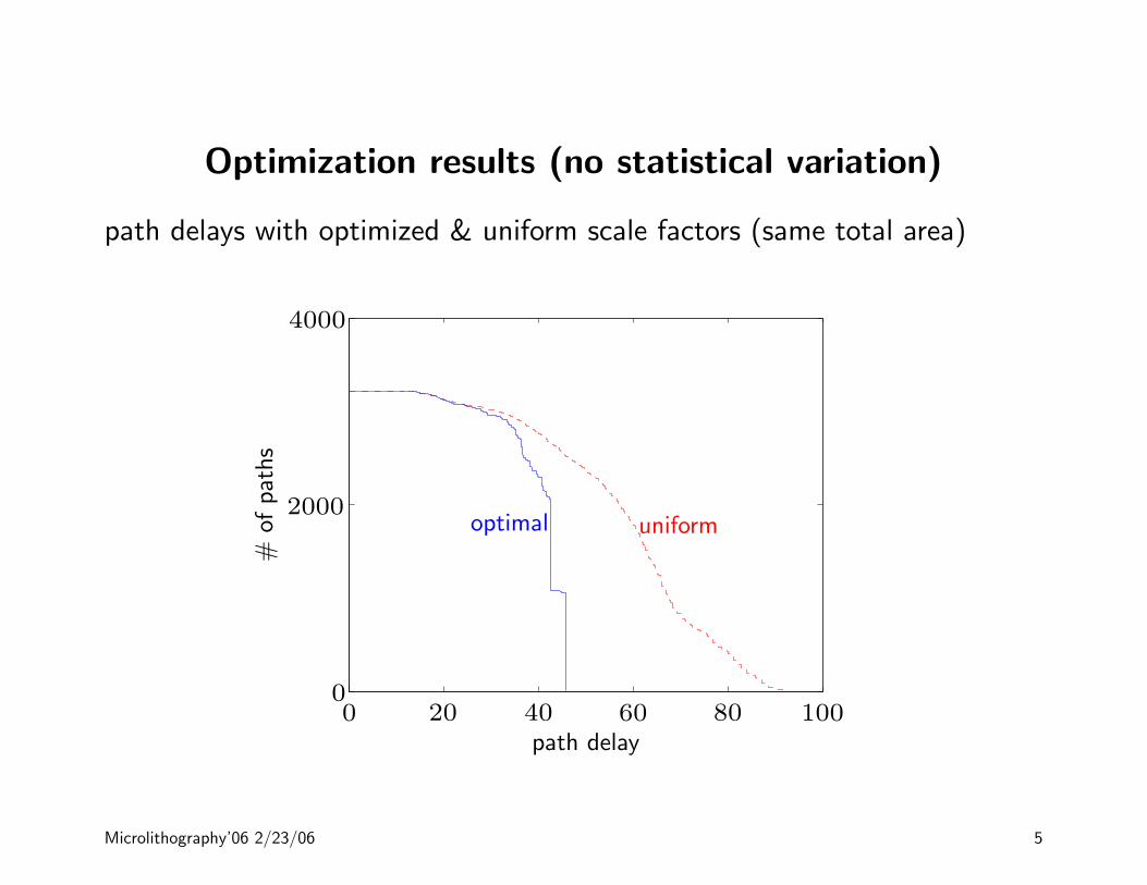
Optimization results (no statistical variation)
path delays with optimized & uniform scale factors (same total area)PSfrag replacements
path delay
#of
pat
hs
0 20 40 60 80 1000
2000
4000
uniformoptimal
Microlithography’06 2/23/06 5

Statistical variation in gate delay
• simple Pelgrom model; larger gates have less (relative) variation in delay
• min sized gate has 10% variation
PSfrag replacements
delay
prob
abili
ty
1 2 3 4 5 6 7
x = 1
x = 2
x = 5
Microlithography’06 2/23/06 6
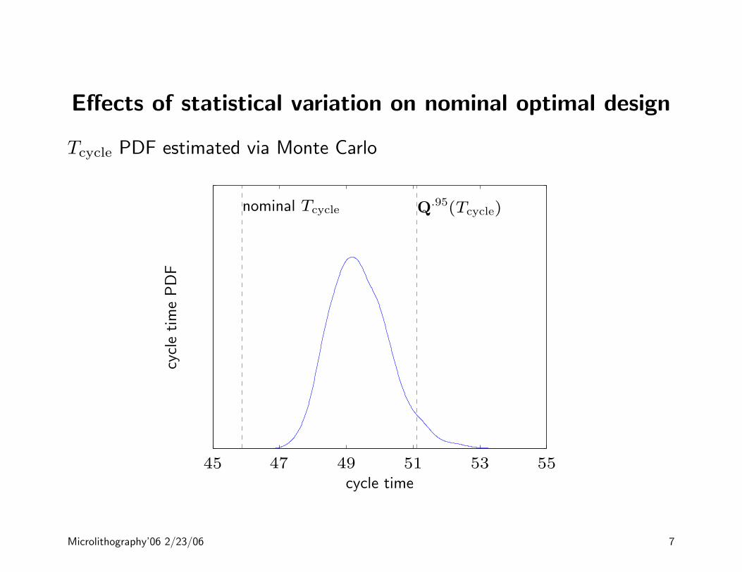
Effects of statistical variation on nominal optimal design
Tcycle PDF estimated via Monte Carlo
PSfrag replacements
cycle time
cycl
etim
ePD
F
45 47 49 51 53 55
nominal Tcycle Q.95(Tcycle)
Microlithography’06 2/23/06 7

Why isn’t Tcycle PDF centered around nominal value?
• Tcycle is max of 3214 random path delays
• max of RVs behaves differently from sum of RVs
– in sum, negative and positive deviations tend to cancel out;PDF is centered, has smaller relative variation
– in max, large deviation of any leads to large value;PDF is shifted, skewed to right, has large relative deviation
Microlithography’06 2/23/06 8
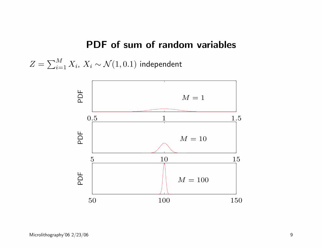
PDF of sum of random variables
Z =∑M
i=1 Xi, Xi ∼ N (1, 0.1) independent
PSfrag replacements
PD
FPD
FPD
F
0.5 1 1.5
5 10 15
50 100 150
M = 1
M = 10
M = 100
Microlithography’06 2/23/06 9

PDF of max of random variables
Z = max{X1, . . . , XM}, Xi ∼ N (1, 0.1) independent
PSfrag replacements
PD
FPD
FPD
F
0.5 1 1.5
M = 1
M = 10
M = 100
Microlithography’06 2/23/06 10

Simple worst-case design
• use slow model for all gates, e.g., 1.2Di
• gives same design
• can we do better?
Microlithography’06 2/23/06 11

Statistically robust design via new method
same circuit, uncertainty model, and constraintsPSfrag replacements
cycle time
distr
ibution
ofcy
cle
tim
e
46 47 48 49 50 51 52 53
nominal optimal design
robust design
Microlithography’06 2/23/06 12

Statistically robust design via new method
nominal delay ED σD Q.95(D)nominal optimal 45.9 49.4 0.91 51.1
robust 46.5 47.6 0.29 48.1
• same circuit, uncertainty model, and constraints
• compared to nominal optimal design, some gates are upsized, others aredownsized
Microlithography’06 2/23/06 13
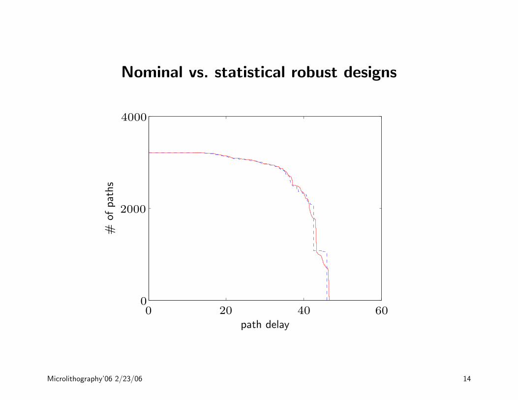
Nominal vs. statistical robust designs
PSfrag replacements
path delay
#of
pat
hs
0 20 40 600
2000
4000
Microlithography’06 2/23/06 14
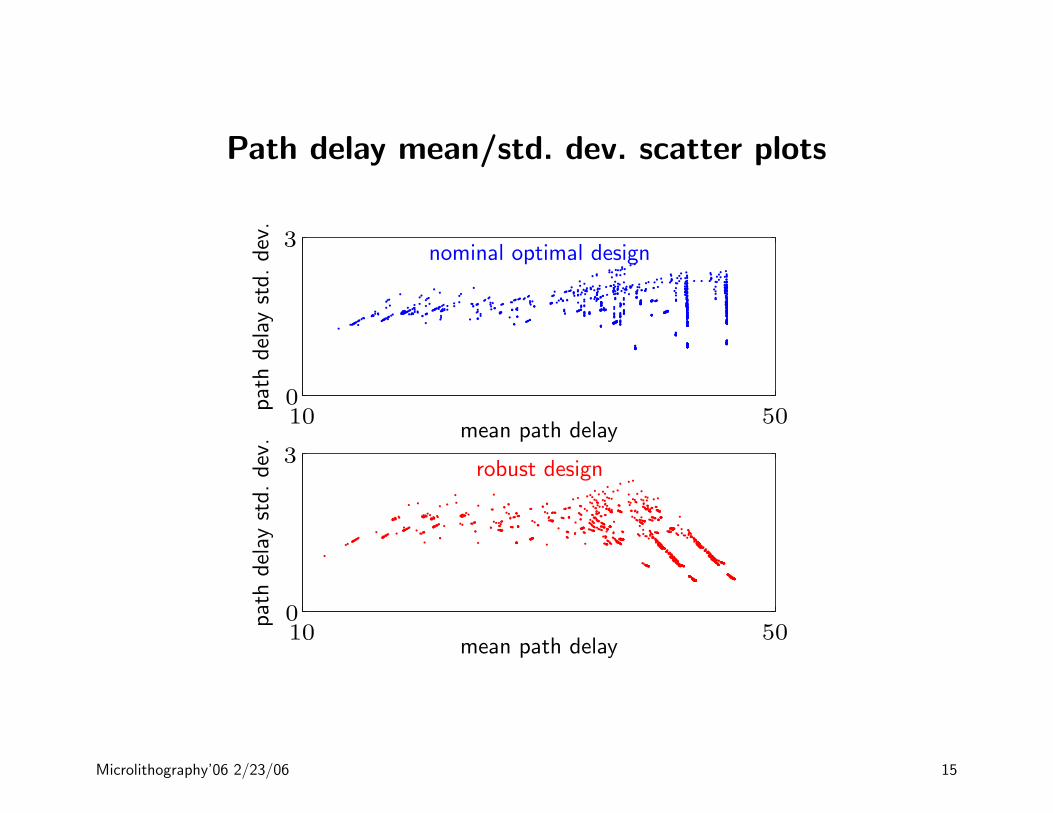
Path delay mean/std. dev. scatter plots
PSfrag replacements
mean path delay
mean path delay
pat
hdel
ayst
d.dev
.pat
hdel
ayst
d.dev
.
10
10
50
50
0
0
3
3nominal optimal design
robust design
Microlithography’06 2/23/06 15

Area/delay trade-off analysis
PSfrag replacements
nominal cycle time
Am
ax
45 55 653000
7000
11000
15000
robust design
nominal optimal design
Microlithography’06 2/23/06 16

Area/delay trade-off analysis
PSfrag replacements
95% cycle time
Am
ax
45 55 653000
7000
11000
15000
robust design nominal optimal design
Microlithography’06 2/23/06 17

Digital Circuit Sizing: Models

Gate scaling
PSfrag replacements
1
2
3
4
5
6
7
input flip flops output flip flops
in out
clock
combinational logic block
RA
RB
RC
CX
CY
• combinational logic; circuit topology & gate types given
• gate sizes (scale factors xi ≥ 1) to be determined
• scale factors affect total circuit area, power and delay
Microlithography’06 2/23/06 18

RC gate delay model
PSfrag replacements
Ri
Ri
Vdd
C ini
C ini
C inti CL
i
• input & intrinsic capacitances, driving resistance, load capacitance
C ini = C in
i xi, C inti = C int
i xi, Ri = Ri/xi, CLi =
∑
j∈FO(i)
C inj
• RC gate delay:Di = 0.69Ri(C
Li + C int
i )
Microlithography’06 2/23/06 19

Path and circuit delay
PSfrag replacements
1
2
3
4
5
6
7
• delay of a path: sum of delays of gates on path
• circuit delay (cycle time): maximum delay over all paths
Microlithography’06 2/23/06 20

Area & power
• total circuit area: A = x1A1 + · · · + xnAn
• total power is P = Pdyn + Pstat
– dynamic power Pdyn =
n∑
i=1
fi(CLi + C int
i )V 2dd
fi is gate switching frequency
– static (leakage) power Pstat =
n∑
i=1
I leaki Vdd
I leaki is leakage current (average over input states)
Microlithography’06 2/23/06 21

Parameters used in example
• model parameters:
gate type C in C int R AINV 3 3 0.48 3
NAND2 4 6 0.48 8NOR2 5 6 0.48 10AOI21 6 7 0.48 17OAI21 6 7 0.48 16
• time unit is τ , delay of min-size inverter (0.69 · 0.48 · 3 = 1)
• area (total width) unit is width of NMOS in min-size inverter
Microlithography’06 2/23/06 22
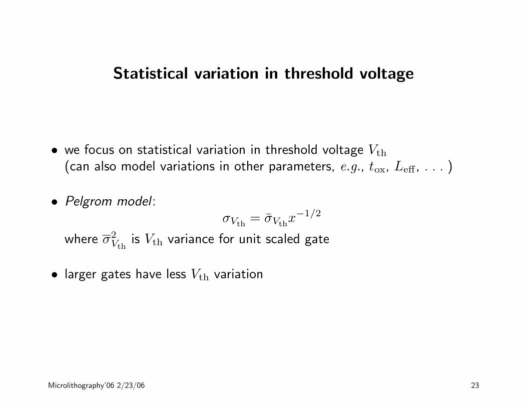
Statistical variation in threshold voltage
• we focus on statistical variation in threshold voltage Vth
(can also model variations in other parameters, e.g., tox, Leff, . . . )
• Pelgrom model :σVth
= σVthx−1/2
where σ2Vth
is Vth variance for unit scaled gate
• larger gates have less Vth variation
Microlithography’06 2/23/06 23
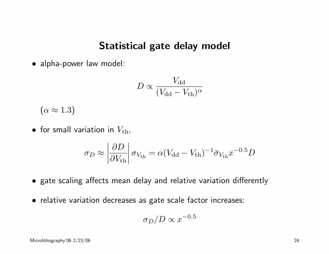
Statistical gate delay model
• alpha-power law model:
D ∝ Vdd
(Vdd − Vth)α
(α ≈ 1.3)
• for small variation in Vth,
σD ≈∣
∣
∣
∣
∂D
∂Vth
∣
∣
∣
∣
σVth= α(Vdd − Vth)
−1σVthx−0.5D
• gate scaling affects mean delay and relative variation differently
• relative variation decreases as gate scale factor increases:
σD/D ∝ x−0.5
Microlithography’06 2/23/06 24

Statistical variation in gate delay
10% relative variation for min sized gate (σD/D = 0.1)inverter driving CL = 4
PSfrag replacements
delay
prob
abili
ty
1 2 3 4 5 6 7
x = 1
x = 2
x = 5
Microlithography’06 2/23/06 25

Statistical variation in gate delay
inverter driving CL = 4PSfrag replacements
scale factor
del
ay
1 2 3 4 50
5τ
10τ
µ − 3σ
µ + 3σ
µ
Microlithography’06 2/23/06 26

Statistical leakage power model
• leakage currentI leak ∝ xe−Vth/V0
(V0 ≈ 0.04)
• linearization does not give accurate prediction of E I leak, σIleak
• exact values for Vth Gaussian:
E I leak = I leak,nomeσ2
Vth/(2V 2
0 x), σIleak =
(
eσ2
Vth/(V 2
0 x) − 1)1/2
E I leak
I leak,nom is leakage current when statistical variation is ignored
Microlithography’06 2/23/06 27
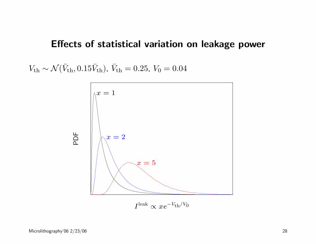
Effects of statistical variation on leakage power
Vth ∼ N (Vth, 0.15Vth), Vth = 0.25, V0 = 0.04
PSfrag replacements
I leak∝ xe−Vth/V0
PD
F
x = 1
x = 2
x = 5
Microlithography’06 2/23/06 28

Statistical variation in leakage power
PSfrag replacements
scale factor
EI
leak/I
leak,n
om
1 2 3 4 51
1.7
Microlithography’06 2/23/06 29

Digital Circuit Sizing: Optimization
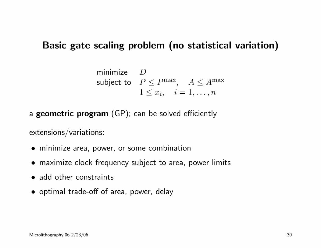
Basic gate scaling problem (no statistical variation)
minimize Dsubject to P ≤ Pmax, A ≤ Amax
1 ≤ xi, i = 1, . . . , n
a geometric program (GP); can be solved efficiently
extensions/variations:
• minimize area, power, or some combination
• maximize clock frequency subject to area, power limits
• add other constraints
• optimal trade-off of area, power, delay
Microlithography’06 2/23/06 30
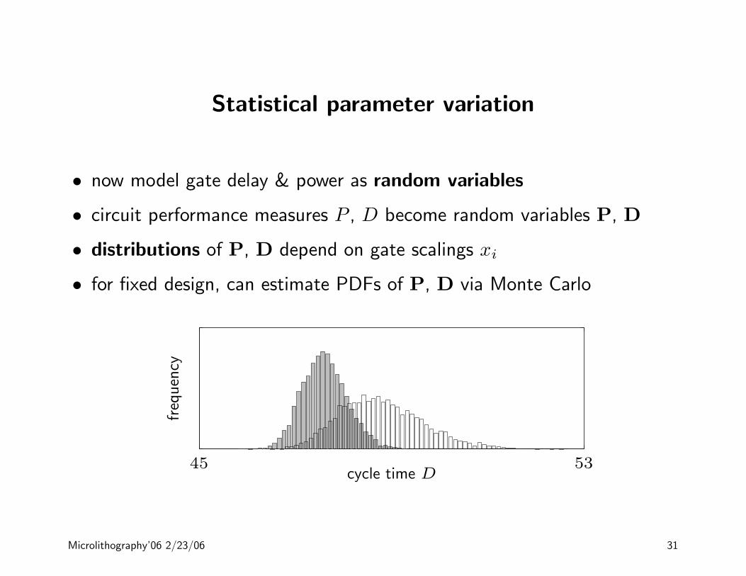
Statistical parameter variation
• now model gate delay & power as random variables
• circuit performance measures P , D become random variables P, D
• distributions of P, D depend on gate scalings xi
• for fixed design, can estimate PDFs of P, D via Monte CarloPSfrag replacements
45 53cycle time D
freq
uen
cy
Microlithography’06 2/23/06 31

Statistical design
• measure random performance measures by 95% quantile (say)
minimize Q.95(D)subject to Q.95(P) ≤ Pmax, A ≤ Amax
1 ≤ xi, i = 1, . . . , n
• extremely difficult stochastic optimization problem; almost noanalytic/exact results
• but, simple heuristic method works well
Microlithography’06 2/23/06 32

The New Method

Statistical power constraint
• total power is sum of gate powers
EP =
n∑
i=1
EPi
• if n is large and P1, . . . ,Pm are independent (enough),
P ≈n
∑
i=1
EPi
• can use EP ≤ Pmax as reasonable approximation of Q.95(P) ≤ Pmax
Microlithography’06 2/23/06 33

Surrogate gate delay
• define surrogate gate delays
Di(x) = Di(x) + κiσi(x)
κiσi(x) is margin on gate delay (κi is typically 2)
PSfrag replacements
scale factor
gate
del
ay µ
µ + κσ
• gives more margin to smaller gates
Microlithography’06 2/23/06 34

Interpretation of gate delay margins
• margins κiσi(x) take statistical gate delay variation into account
• κi related to Prob (Di ≤ µi + κiσi)
– Chebyshev inequality:
Prob (Di ≤ µi + κiσi) ≥κ2
i
1 + κ2i
– if Di is Gaussian
Prob (Di ≤ µi + κiσi) =1√2π
∫
∞
κi
e−t2/2 dt
Microlithography’06 2/23/06 35

Heuristic for statistical design
• use modified (leakage) power model taking into account statisticalvariation
• use surrogate gate delays Di(x) = Di(x) + κiσi(x)
• now solve resulting (deterministic) gate scaling problem
• verify statistical performance via Monte Carlo analysis
(can update κi’s and repeat)
Microlithography’06 2/23/06 36

Digital Circuit Sizing Example
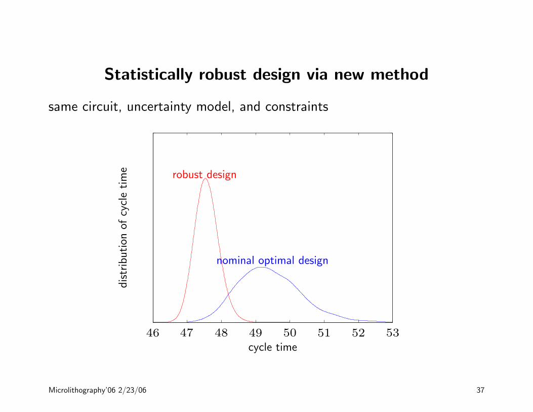
Statistically robust design via new method
same circuit, uncertainty model, and constraintsPSfrag replacements
cycle time
distr
ibution
ofcy
cle
tim
e
46 47 48 49 50 51 52 53
nominal optimal design
robust design
Microlithography’06 2/23/06 37

Path delay mean/std. dev. scatter plots
PSfrag replacements
mean path delay
mean path delay
pat
hdel
ayst
d.dev
.pat
hdel
ayst
d.dev
.
10
10
50
50
0
0
3
3nominal optimal design
robust design
Microlithography’06 2/23/06 38
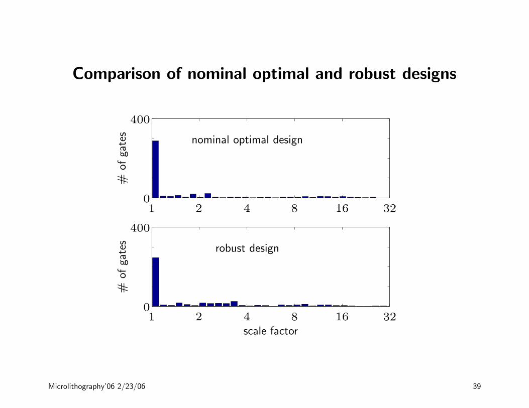
Comparison of nominal optimal and robust designs
PSfrag replacements
#of
gate
s
scale factor
#of
gate
s
1
1
2
2
4
4
8
8
16
16
32
32
0
0
400
400
nominal optimal design
robust design
Microlithography’06 2/23/06 39
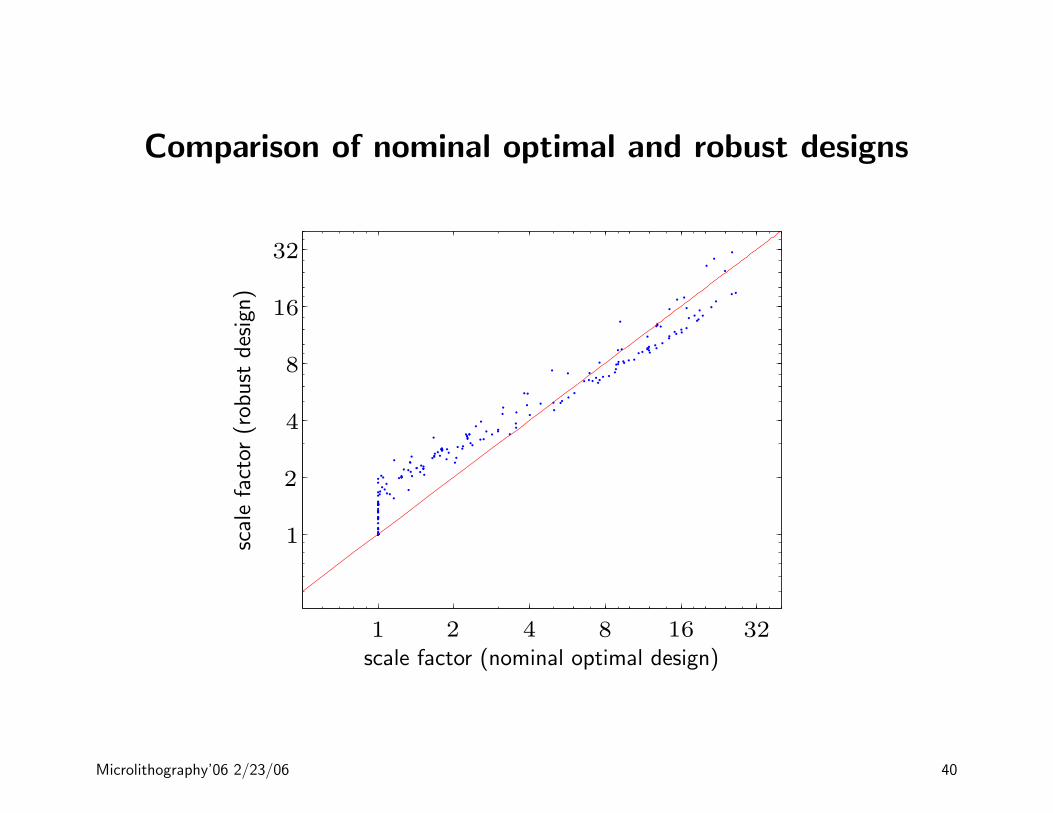
Comparison of nominal optimal and robust designsPSfrag replacements
scale factor (nominal optimal design)
scal
efa
ctor
(rob
ust
des
ign)
1 2 4 8 16 32
1
2
4
8
16
32
Microlithography’06 2/23/06 40
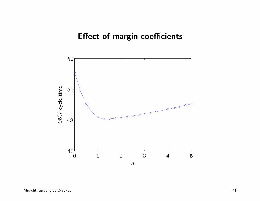
Effect of margin coefficients
PSfrag replacements
κ
95%
cycl
etim
e
0 1 2 3 4 546
48
50
52
Microlithography’06 2/23/06 41

Sensitivity to model assumptions
question: how sensitive is robust design to our model of process variation?
• distribution shape
• correlation between gates
• Pelgrom model of variance vs. scale factor
answer: not very
Microlithography’06 2/23/06 42

Simulation with uniform gate delay distributions
PSfrag replacements
cycle time
distr
ibution
ofcy
cle
tim
e
46 47 48 49 50 51 52 53
nominal optimal design
robust design
compared with Gaussian gate delays:nominal optimal design not quite as bad; robust design still quite good
Microlithography’06 2/23/06 43
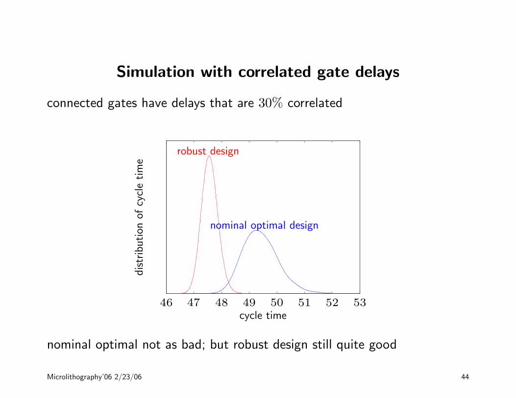
Simulation with correlated gate delays
connected gates have delays that are 30% correlated
PSfrag replacements
cycle time
distr
ibution
ofcy
cle
tim
e
46 47 48 49 50 51 52 53
nominal optimal design
robust design
nominal optimal not as bad; but robust design still quite good
Microlithography’06 2/23/06 44

Conclusions and Future Work

Conclusions
• statistically robust design is subtle; cannot be done by hand
• exact or direct methods will not work well
– computationally intractable– depend on details of statistical models
• heuristic method is relatively simple, scales well, gives good designs
– reduces problem to a deterministic one
Microlithography’06 2/23/06 45
References
• Boyd, Kim, and Mohan, DATE Tutorial 2005
Geometric programming and its applications to EDA problems
• Boyd, Kim, Patil, and Horowitz, SPIE ML 2006
A heuristic method for statistical digital circuit sizing
• Kim, Boyd, Patil, and Horowitz, Optimization and Engineering, 2006A heuristic for optimizing stochastic activity networks with applicationsto statistical digital circuit sizing
• Boyd, Kim, Patil, and Horowitz, Operations Research, 2005Digital circuit optimization via geometric programming
• Patil, Yun, Kim, Cheung, Horowitz, and Boyd, ISQED 2005
A new method for design of robust digital circuits
all available from www.stanford.edu/∼boyd/research.html
Microlithography’06 2/23/06 46
References (continued)
• Mani, Devgan, Orshansky, DAC 2005
An efficient algorithm for statistical minimization of total power undertiming yield constraints
• Satish, Ravindran, Moskewicz, Chinnery, and Keutzer, UCB tech.
report, 2005
Evaluating the effectiveness of statistical gate sizing for poweroptimization
• Bhardwaj and Vrudhula, DAC 2005
Leakage minimization of nano-scale circuits in the presence ofsystematic and random variations
Microlithography’06 2/23/06 47