a frequency synthesizer for a radio-over-fiber...
TRANSCRIPT

A Frequency Synthesizer for a
Radio-Over-Fiber Receiver
By Mark Houlgate
Supervisor: Professor Len MacEachern
A report submitted in partial fulfillment of the requirements
of the 4th Year Engineering Project
Department Electronics Faculty of Engineering
Carleton University
April, 2003

ABSTRACT
As cellular telephone networks continue to grow to meet increasing demand, new solu-
tions are being suggested to simplify base-stations and to facilitate upgrades. Radio-
over-fiber architectures can be used to simplify base-stations by modulating radio-signals
directly onto an optical fiber link to a central office responsible for all signal processing.
One of the key elements in the radio-over-fiber receiver is the frequency synthesizer,
which generates the local oscillator signal used by the mixer to down-convert the radio
signal to an appropriate frequency for transmission.
The frequency synthesizer was implemented using a charge-pump based phase-
locked loop with a tri-state phase/frequency detector and a programmable pulse-swallow
frequency divider. Since the required frequency of operation can be as high as 1.4GHz,
the speed of the digital logic used in the frequency divider is a critical design factor. A
custom library of digital logic gates was designed using MOS current-mode logic
(MCML). These gates were designed to operate at frequencies up to 1.4GHz.
This report outlines the design of the phase/frequency detector and the programmable
pulse-swallow frequency divider. The design, layout, and simulation of the MCML logic
family are also presented.

ACKNOWLEDGEMENTS
I would like to thank the many people who helped me with this project in the last 8
months. First, many thanks are owed to the rest of the radio-over fiber project group:
Fiona, James, Mike, Dan, Nigel, Jackson, and Aaron. During the course of the project, I
could always count on each and every one of these individuals for support and advice. I
am grateful that they were willing to act as “sounding boards” for my ideas, some of
which actually made it into the final project. In addition, I would like to thank Wilson
Kwan who successfully demonstrated that optimized versions of my MCML logic gates
could operate at speeds up to about 10GHz, and Professor Knight, who provided help
with the reset capability of my D-latch. Next, a great debt of gratitude is owed to Nagui
Mikhail for his tireless hours of technical support, and for his work in setting up a com-
fortable and useful lab.
Finally, I would like to thank Professor Len MacEachern who provided me with support,
advice, and an excellent working environment. His undying sense of humour and his
constant faith in my work made the long hours “fun.”

TABLE OF CONTENTS
1 Introduction................................................................................................................. 1
1.1 Radio-Over-Fiber Architecture............................................................................... 1
1.2 Frequency Synthesizer ............................................................................................ 2
1.3 Structure of the Report............................................................................................ 4
2 Phase/Frequency Detector .......................................................................................... 5
2.1 Theory..................................................................................................................... 5
2.2 Implementation ....................................................................................................... 7
2.3 Simulation Results .................................................................................................. 9
3 Programmable Frequency Divider............................................................................ 11
3.1 Overview............................................................................................................... 11
3.2 Dual-Modulus Prescaler ....................................................................................... 13
3.2.1 Theory........................................................................................................... 13
3.2.2 Implementation ............................................................................................. 14
3.3 Program Counter................................................................................................... 16
3.3.1 Theory........................................................................................................... 16
3.3.2 Implementation ............................................................................................. 17
3.3.3 Simulation Results ........................................................................................ 19
3.4 Swallow Counter................................................................................................... 20
3.4.1 Theory........................................................................................................... 20
3.4.2 Implementation ............................................................................................. 21
3.4.3 Simulation Results ........................................................................................ 22
3.5 Simulation of Frequency Divider.......................................................................... 23

4 MOS Current Mode Logic (MCML) ........................................................................ 25
4.1 Introduction........................................................................................................... 25
4.2 Theory................................................................................................................... 26
4.3 Inverter/Buffer ...................................................................................................... 28
4.4 OR/NOR ............................................................................................................... 34
4.5 AND/NAND ......................................................................................................... 37
4.6 XOR/XNOR.......................................................................................................... 40
4.7 D-Latch ................................................................................................................. 43
4.8 D-Flip-flop ............................................................................................................ 45
5 Recommendations..................................................................................................... 49
6 Conclusions............................................................................................................... 50
7 References................................................................................................................. 51
LIST OF FIGURES
Figure 1 Radio-Over-Fiber Receiver Architecture ............................................................. 2
Figure 2 Frequency Synthesizer Architecture .................................................................... 3
Figure 3 State Diagram of the Phase/Frequency Detector.................................................. 6
Figure 4 Implementation of the Phase/Frequency Detector ............................................... 8
Figure 5 Cadence Schematic of the Phase/Frequency Detector ......................................... 9
Figure 6 PFD Simulation Results (Equal Frequencies) .................................................... 10
Figure 7 PFD Simulation Results (Different Frequencies)............................................... 10
Figure 8 Pulse-Swallow Frequency Divider ..................................................................... 12
Figure 9 Implementation of a 15/16 Dual-Modulus Prescaler.......................................... 14
Figure 10 Cadence Schematic of the 15/16 Dual-Modulus Prescaler .............................. 15
Figure 11 Simulation Results for the Dual Modulus Prescaler (Modulus Control =0) .... 15
Figure 12 Block Diagram of a 7-bit Program Counter ..................................................... 16
Figure 13 Cadence Schematic showing the overall structure of the 7-Bit Program Counter
.................................................................................................................................. 19
Figure 14 Program Counter Simulation Results ............................................................... 20
Figure 15 Block Diagram of a 6-Bit Swallow Counter .................................................... 21
Figure 16 Cadence Schematic showing the overall structure of the 6-Bit Swallow Counter
.................................................................................................................................. 22
Figure 17 Swallow Counter Simulation Results (S=20)................................................... 23
Figure 18 Frequency Divider Simulation Results (Fin=800MHz, DIV=800).................. 24
Figure 19 Ideal MCML Logic Gate [2] ............................................................................ 27
Figure 20 Schematic of an MCML Inverter/Buffer.......................................................... 29
Figure 21 Layout of MCML Inverter/Buffer .................................................................... 32
Figure 22 Post-Layout Simulation of the MCML Inverter/Buffer ................................... 33
Figure 23 Schematic of an MCML OR/NOR Gate .......................................................... 35
Figure 24 Layout of the MCML OR/NOR Gate............................................................... 36
Figure 25 Post-layout Simulation Results for the MCML OR/NOR................................ 36
Figure 26 Schematic of an MCML AND/NAND Gate .................................................... 38
Figure 27 Layout of an MCML AND/NAND Gate ......................................................... 39
Figure 28 Post-layout Simulation Results of the AND/NAND Gate ............................... 39
Figure 29 Schematic of an MCML XOR/XNOR Gate..................................................... 41
Figure 30 Layout of an MCML XOR/XNOR Gate.......................................................... 42
Figure 31 Post-layout Simulation Results for the XOR/XNOR ....................................... 42
Figure 32 Schematic of an MCML D-Latch (with Reset) ................................................ 43
Figure 33 Layout of an MCML D-Latch (with Reset) ..................................................... 44
Figure 34 Post-layout Simulation Results of the MCML D-Latch................................... 45
Figure 35 Schematic of the Phase/Frequency Detector D-Flip-flop................................. 46
Figure 36 Schematic of a General D-Flip-flop ................................................................. 47
Figure 37 Post-layout Simulation Results of the MCML D-Flip-flop.............................. 48

LIST OF TABLES
Table 1 Inverter/Buffer Performance Measurements ....................................................... 34
Table 2 OR/NOR Performance Measurements................................................................. 37
Table 3 AND/NAND Performance Results...................................................................... 40
Table 4 XOR/XNOR Performance Measurements........................................................... 41
Table 5 D-Flip-flop Performance Measurements ............................................................. 48

1
1 INTRODUCTION
1.1 Radio-Over-Fiber Architecture
As consumer demand for cellular telephones continues to increase, service provid-
ers are constantly expanding coverage areas and offering new features. This period of
growth has seen a rapid increase in the number of base-stations and frequent changes to
transmission protocols. Since current base-stations are often responsible for the demodu-
lation and processing of cellular signals, protocol changes require updates to software
and/or hardware in the multitude of existing base-stations. In addition, the increasing
complexity of the base-stations has resulted in the need for large, power-hungry equip-
ment.
Utilizing a radio-over-fiber architecture is one solution that has been suggested to
simplify base-stations and to facilitate upgrades. In a radio-over-fiber system, each base-
station is responsible for receiving an analog RF signal, converting it into the optical do-
main, and transmitting the information over an optical fiber to a centralized control sta-
tion. The control station, which is connected by fiber to many other base-stations, is then
responsible for the demodulation and processing of the signal. Using this architecture, all
protocol information is centralized and the simplified base-stations do not need to be up-
dated when changes are made. On the transmit path, the control station sends an optical
signal to the base-station, which in turn converts it back into the electrical domain for
transmission from its antenna.
The basic receiver architecture of this system is shown in Figure 1. The Low-
Noise-Amplifier (LNA) is responsible for amplifying the received signal and passing it to

2
the mixer. The mixer then down-converts the signal to a frequency suitable for transmis-
sion over the optical fiber. Next, the down-converted signal is passed to the pre-distorter,
which compensates for the non-linear distortion that occurs when the laser is modulated.
Finally, the frequency synthesizer provides the local-oscillator signal used by the mixer.
As a result, it can also be used to choose the frequency to be received.
Figure 1 Radio-Over-Fiber Receiver Architecture
The receiver used in this project was designed to receive signals from 3 bands at
1.8 GHz, 1.9 GHz, and 2.4 GHz, with an intermediate frequency (IF) of 1 GHz, chosen to
minimize dispersion in the optical link. As a result, the frequency synthesizer was de-
signed to provide local oscillator signals at 800 MHz, 900 MHz, and 1.4 GHz.
Aaron Wrightly designed the LNA, Mike Gordon designed the mixer, Nigel An-
toine, Fiona Shearer, and James McGale designed the pre-distorter, and Jackson Hamil-
ton designed the band-gap voltage reference used by the entire receiver. Finally, Daniel
Olszewski and I designed the frequency synthesizer.
1.2 Frequency Synthesizer
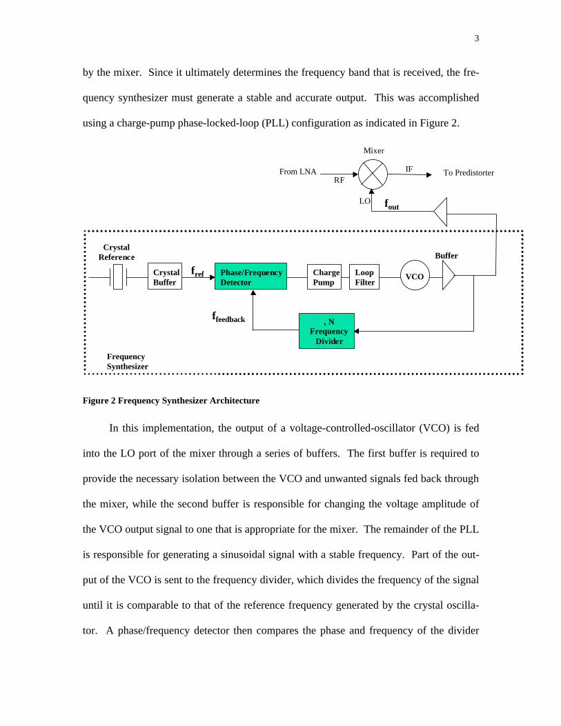
The frequency synthesizer is responsible for creating the local oscillator signal used
3
by the mixer. Since it ultimately determines the frequency band that is received, the fre-
quency synthesizer must generate a stable and accurate output. This was accomplished
using a charge-pump phase-locked-loop (PLL) configuration as indicated in Figure 2.
CrystalReference
CrystalBuffer
Phase/FrequencyDetector
ChargePump
LoopFilter
VCO
Buffer
÷NFrequency
Divider
Mixer
RF
LO
IF To PredistorterFrom LNA
FrequencySynthesizer
fref
fout
ffeedback
Figure 2 Frequency Synthesizer Architecture
In this implementation, the output of a voltage-controlled-oscillator (VCO) is fed
into the LO port of the mixer through a series of buffers. The first buffer is required to
provide the necessary isolation between the VCO and unwanted signals fed back through
the mixer, while the second buffer is responsible for changing the voltage amplitude of
the VCO output signal to one that is appropriate for the mixer. The remainder of the PLL
is responsible for generating a sinusoidal signal with a stable frequency. Part of the out-
put of the VCO is sent to the frequency divider, which divides the frequency of the signal
until it is comparable to that of the reference frequency generated by the crystal oscilla-
tor. A phase/frequency detector then compares the phase and frequency of the divider

4
output and the reference signal, and provides an output that is proportional to their differ-
ence. This “error signal” is conditioned by the charge-pump and a low-pass loop-filter
after which it is used to change the output frequency of the VCO. The feedback loop as-
sures that the VCO will eventually lock on a multiple of the reference signal, where the
exact multiple is determined by the divisor used in the frequency divider. Therefore, the
output frequency is determined by [3]:
fout = Nfref (1)
As a result, the choice of reference frequency determines the minimum channel
separation. If the resolution provided by the crystal reference is insufficient, an
additional frequency divider could be added between the crystal buffer and the
phase/frequency detector. For the remainder of this report, a 1 MHz reference frequency
is assumed. However, if this were increased to 10 MHz to match available crystals, the
design would remain the same, provided the division ratios are adjusted accordingly, or
that an extra frequency divider is used at the input.
Dan designed the charge pump, loop filter, VCO, and VCO buffer. I was
responsible for the design of the phase/frequency detector, the programmable frequency
divider, and the digital logic library used to implement these components.
1.3 Structure of the Report
Section 2. Phase/Frequency Detector. This section discusses the theory, design, and
implementation of the phase/frequency detector. Theory, schematics, and simulation re-
sults are presented.
Section 3. Programmable Frequency Divider. The design and implementation of the
programmable frequency divider are discussed. The design is sub-divided into smaller

5
components whose schematics and simulation results are presented. Finally, the results
of a complete simulation are provided.
Section 4. MOS Current Mode Logic (MCML). This section provides an overview of
the design and implementation of an MCML digital logic family. These MCML compo-
nents are used as the building blocks for the rest of the design.
Section 5. Recommendations. Improvements to the design are suggested, and alternate
implementations are briefly explored.
Section 6. Conclusions. The work accomplished in the project is summarized.
2 PHASE/FREQUENCY DETECTOR
2.1 Theory
As introduced in the previous section, the phase/frequency detector (PFD) provides
the comparison mechanism for the phase-locked loop. Its purpose is to simultaneously
compare the phase and frequency of the crystal reference signal to that of the signal at the
output of the programmable frequency divider. It generates an output signal that is pro-
portional to their difference. Although many PLLs can accomplish this task with a sim-
ple phase detector, a detector capable of simultaneously measuring both phase and fre-
quency decreases the acquisition time of the loop.
In the case of a charge-pump PLL, the phase/frequency detector actually outputs
two signals: UP and DOWN. The UP signal indicates that the VCO frequency should be
increased, while the DOWN signal indicates that the frequency should be decreased.
These signals are used by switches in the charge pump to charge, or discharge a capaci-
tor, thereby increasing, or decreasing its output control voltage. As a result, the duration

6
of the UP and DOWN signals determines how much charge is transferred, and the mag-
nitude of change in the control voltage. For large differences in the phase or frequency of
the input signals, the duration of the corresponding PFD output signal is large. This con-
cept is best illustrated by examining the PFD used in this receiver.
Figure 3 shows the state diagram of the tri-state PFD used in this project.
Figure 3 State Diagram of the Phase/Frequency Detector
As indicated in Figure 3, the PFD maintains 3 states: a ‘reset’ state in which nei-
ther of the two signals is asserted, an UP state, and a DOWN state. State transitions oc-
cur on the rising edges of the reference and feedback signals. As a result, this implemen-
tation measures phase and frequency by the relative occurrences of edges in the signals
and is duty-cycle independent. This duty-cycle independence is crucial for the proper
operation of the frequency synthesizer since the programmable frequency divider used in
this project does not output a fifty-percent duty cycle.
To understand how phase-detection occurs, it is useful to investigate the state tran-
sitions when the loop is locked and the two frequencies are equal. Initially, the PFD is in
its ‘reset’ state and UP and DOWN are both low. On the rising edge of one of the input
signals (say the reference signal), the PFD moves to the UP state and asserts the signal.
Since both signals have the same frequency, the next edge to occur is that of the feedback
7
signal. When this edge is detected, the PFD returns to the reset state until the next refer-
ence edge causes the UP signal to be asserted once again. If the first edge to occur were
on the feedback signal instead of the reference, the equivalent loop would occur into and
out of the DOWN state. As a result, the UP or DOWN signal is high for a duration equal
to the phase difference between the two signals with the particular output indicating
which signal is leading the other. This behaviour is indicated in Figure 6. However,
since the finite width of the pulses causes the control voltage from the charge-pump to
change, the VCO will modify its frequency and the loop will eventually acquire a zero
phase difference.
Similarly, this implementation of a PFD achieves frequency detection by counting
the relative number of edges in the signal. If the frequency of the reference signal is
higher than that of the feedback signal, the UP signal remains high for numerous cycles
of the reference, indicating that the VCO should increase its frequency. When an edge is
finally detected on the feedback signal, the PFD briefly returns to the ‘reset’ state until
the next edge of the reference signal returns the PFD to the UP state. The larger the fre-
quency difference, the greater the proportion of time that the UP signal is high. Similar
logic can be applied to the case where the frequency of the feedback signal is higher, and
the DOWN signal is asserted. This behaviour is demonstrated in Figure 7.
2.2 Implementation
The state diagram in Figure 3 can be closely approximated using the circuit shown in
Figure 4. The circuit is comprised of two D-type flip-flops whose inputs are tied to logic
‘1’, and whose outputs correspond to the UP and DOWN signals. Their clock inputs are
tied to the input signals, and their asynchronous reset ports are tied to the logical AND of

8
the two output signals.
Figure 4 Implementation of the Phase/Frequency Detector
When an edge is detected on either of the two signals, the corresponding flip-flop
drives its output high, where it remains until it is reset. This reset occurs when an edge
on the complementary signal is detected, driving its flip-flop high. At this point, the out-
put of the AND gate becomes high, resetting the two flip-flops. Since this implementa-
tion allows both inputs to be high simultaneously for the brief duration of the reset, it is
not exactly equal to the state diagram proposed in Figure 3. However, the remainder of
the operation remains the same as discussed in the previous section.
An interesting problem occurs when the phase of the two signals approaches zero.
This condition, known as the “dead zone” could lead to erroneous operation if the reset
occurs before both signals have stabilized [3]. In this case, one of the flip-flops may reset
faster than the other, and the initial rising edge, which was not completed, could end up
driving one of the flip-flops high. This problem can be alleviated by adding extra delay
to the reset path in the form of a chain of delay buffers. However, care must be taken to
not increase the delay too much, as both signals would then be high simultaneously for a

9
longer period of time.
To reject common-mode noise, and to ease integration with the frequency divider,
the PFD was built using differential logic components. The design and implementation
of these components is discussed in Section 4 on MCML logic. The final schematic of
the PFD, as entered into Cadence, is shown in Figure 5. This schematic shows the use of
differential logic and custom flip-flops whose inputs are internally tied high.
Figure 5 Cadence Schematic of the Phase/Frequency Detector
2.3 Simulation Results

10
The schematic indicated in Figure 5 was simulated in Cadence using the Spectre
simulation tool. Figure 6 shows the resulting waveforms for the case when the frequen-
cies are equal, and Figure 7 shows the results for different frequencies.
Figure 6 PFD Simulation Results (Equal Frequencies)
Figure 7 PFD Simulation Results (Different Frequencies)
Figure 6 successfully demonstrates the theory discussed in section 2.1. In this case,

11
the Reference signal leads Feedback, and pulses appear on the UP line with a width
equal to the phase difference between the two signals. In addition, the brief resetting
pulses can be seen on the DOWN line, corresponding to the rising edges of the Feedback
signal. In addition, Figure 7 successfully demonstrates the behaviour of the PFD when
the frequencies are different. In this case, Feedback is at a higher frequency, and wide
pulses are generated on the DOWN line, interrupted only by the brief resetting pulses on
the UP line corresponding to the rising edges of the Reference signal. These waveforms
confirm the successful design and implementation of the phase/frequency detector.
3 PROGRAMMABLE FREQUENCY DIVIDER
3.1 Overview
The programmable frequency divider is used in the frequency synthesizer to control
the output frequency by means of the relation fout = N*fref, where N is the division ratio
and fref is the reference frequency provided by the crystal. As indicated in Figure 2, the
frequency divider closes the feedback path between the output of the VCO buffer and the
phase/frequency detector discussed in the previous section. Since the output frequency of
the VCO must operate at frequencies up to 1.4GHz, the frequency detector must also be
capable of operating at this speed. Since the digital logic required to implement the pro-
grammable divisor adds a significant number of gate delays, the frequency divider was
implemented in a standard pulse-swallow configuration, as illustrated in Figure 8.

12
Figure 8 Pulse-Swallow Frequency Divider
The pulse-swallow configuration solves this problem by using a dual-modulus
prescaler (DMP) to generate a slower signal (SlowCLK) which is passed to the pro-
grammable portion of the frequency divider, implemented using a program counter and a
swallow counter. Unlike the program counter or the swallow counter, which must
change their division ratios based on user-provided control signals, the DMP always di-
vides the signal by either 15 or 16, depending on the value of modulus control. As a re-
sult, the required logic is much simpler, and the DMP can easily be designed to function
at 1.4 GHz using the custom-designed MCML logic gates discussed later in this report.
Assuming a worst-case scenario in which the VCO frequency is 1.4GHz and the modulus
of the DMP is 15, the highest frequency seen by the program counter and swallow coun-
ter is only about 93 MHz. At this lower frequency, the programmable counters can ade-
quately function.
To understand how the architecture in Figure 8 can function as a programmable
divider, it is useful to examine the complete operation of the circuit in the time required

13
to generate one cycle of the output signal. Initially, the DMP divides the frequency of the
VCO signal by N+1. After S pulses of SlowCLK, the swallow counter (SC) asserts
modulus control, changing the modulus of the DMP to N. At this point in the cycle, the
program counter (PC) has also counted S pulses of SlowCLK, or S(N+1) cycles of the
VCO signal. The PC counter then counts the remaining (P-S) pulses of SlowCLK, corre-
sponding to N(P-S) pulses of the VCO signal, and outputs a pulse to the PFD. This pulse
is also used to reset the counts of the program counter and swallow counter, while return-
ing modulus control to its initial state. Using the above analysis, it is evident that an
output pulse is generated every S(N+1) + N(P-S) cycles of the VCO signal. As a result,
the overall division ratio of the circuit can be expressed as:
DIV = S(N+1)+N(P-S) = NP+S, (2)
where P is specified by a 7-bit control signal, and S is specified by a 6-bit control signal
[3]. It is important to note that for the pulse-swallow frequency divider to operate, S must
be less than P. If this were not the case, the DMP would divide by N+1 for the entire cy-
cle and the division ratio would reduce to (N+1)P.
The remainder of this section discusses the design and simulation of the three
blocks of Figure 8. In addition, overall simulation results are presented in section 3.5.
3.2 Dual-Modulus Prescaler
3.2.1 Theory
As discussed in section 3.1, the dual-modulus prescaler (DMP) divides the VCO
frequency by either N, or N+1, depending on the value of modulus control. In this pro-
ject, N was chosen to be 15 and the circuit was designed to divide by 16 when modulus
14
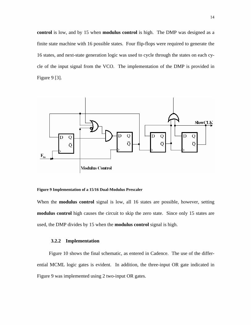
control is low, and by 15 when modulus control is high. The DMP was designed as a
finite state machine with 16 possible states. Four flip-flops were required to generate the
16 states, and next-state generation logic was used to cycle through the states on each cy-
cle of the input signal from the VCO. The implementation of the DMP is provided in
Figure 9 [3].
Figure 9 Implementation of a 15/16 Dual-Modulus Prescaler
When the modulus control signal is low, all 16 states are possible, however, setting
modulus control high causes the circuit to skip the zero state. Since only 15 states are
used, the DMP divides by 15 when the modulus control signal is high.
3.2.2 Implementation
Figure 10 shows the final schematic, as entered in Cadence. The use of the differ-
ential MCML logic gates is evident. In addition, the three-input OR gate indicated in
Figure 9 was implemented using 2 two-input OR gates.

15
Figure 10 Cadence Schematic of the 15/16 Dual-Modulus Prescaler
Figure 11 provides the simulation results for the DMP with modulus control set to logic
‘0’. As expected, the frequency of SlowCLK is equal to the input frequency divided by
16. These results suggest that the dual-modulus prescaler operates as designed and in-
tended.
Figure 11 Simulation Results for the Dual Modulus Prescaler (Modulus Control =0)

16
3.3 Program Counter
3.3.1 Theory
As described in section 3.1, the program counter is responsible for counting P
pulses of SlowCLK before outputting a pulse to the phase/frequency detector and reset-
ting itself and the swallow counter. The implementation used in this project, using a 7-bit
ripple counter, a 7-bit comparator, and a zero-detector is shown in Figure 12. The ripple
counter is clocked by SlowCLK, and increments its count by one each clock cycle. At
each stage, the 7-bit comparator compares each count bit to the corresponding bit in the
control signal, and outputs a 0 for each equal bit. When the zero-detector detects equiva-
lence in all of the 7 bits, indicating that the desired count has been reached, Fout is driven
high. On the next clock cycle, the program counter is reset to zero and the count is re-
started. In addition, the output pulse on Fout is used to reset the count of the swallow
counter, indicating the end of one complete cycle of the frequency divider.
Figure 12 Block Diagram of a 7-bit Program Counter

17
The ripple counter is implemented using 7 cascaded D-type flip-flops, each ar-
ranged in a toggle configuration. The output of each flip-flop is used to clock the next
flip-flop. Since the output of each flip-flop inverts on every clock cycle, each flip-flop
essentially divides its clock by two, causing the next stage of the ripple counter to be
clocked at half the rate of the previous flip flop. Each flip-flop was designed to respond
to the falling edge of its clock, when the output of the previous stage changes from a 1 to
a 0. In this way, an incrementing binary count is achieved with the outputs of each flip-
flop forming the bits of the count. Since the program counter contains 7-bits, any count
between 0 and 127 can be set by the control signal. It is important to realize however that
in order to achieve a division ratio as specified in the equation DIV=NP+S, the control
signal must be set to P-1, since the zero-state is included in the count.
3.3.2 Implementation
The final schematic of the program counter is provided in Figure 13. Looking at
Figure 13, it is possible to see the three major components of the program counter im-
plemented using MCML logic gates. At the input of the counter, an array of 7 flip-flops
is used as the ripple counter. The outputs of the ripple counter, taken from the outputs of
each of the flip-flops, are fed into an array of 7 XNOR gates. The XNOR gates compare
each bit with the corresponding bit in the control signal, outputting a logical ‘1’ when the
bits are equal. Although this logic is inverted compared to the description of the com-
parator in the previous section, the zero-detector is implemented as a one-detector using a
tree of cascaded AND gates. In this way, the overall logic of the circuit is unchanged,
and the output pulse can be generated without any additional logic.
Another difference seen in Figure 13 is a separate output, SwallowRST, and some
18
simple circuitry used to generate it. SwallowRST is used internally to reset the flip-flops
of the program counter, and externally to reset the flip-flops of the swallow counter.
Since the fan-out of the reset signal is high (7 flip-flops in the PC, and 6 in the SC), the
reset signal is broken into two paths and driven using separate MCML buffers. In early
simulations, these buffers were absent and the reset signal could not provide enough cur-
rent to drive the input capacitance associated with the flip-flops. SwallowRST was gen-
erated using an approach that guarantees predictable timing of the reset signal. Fout is
“tapped” and fed to the input of a flip-flop clocked by Fin. On the clock cycle immedi-
ately following Fout going high, the pulse is sampled by the flip-flop, generating Swal-
lowRST and resetting both the program counter and the swallow counter. To ensure that
the reset signal is removed before the next clock cycle, the reset signal is fed back to its
generating flip-flop through a delay chain comprised of three buffers. This delay chain
must be longer than the time required to reset all flip-flops to guarantee that all flip-flops
are reset before revoking the signal.
One final element of the reset generator is the OR gate placed between the output
of the reset flip-flop and the output buffers. This OR gate allows SwallowRST to be
generated normally as part of the operation of the circuit, or when a “hard” reset is pro-
vided from an external source, such as on power-up.

19
Figure 13 Cadence Schematic showing the overall structure of the 7-Bit Program Counter
3.3.3 Simulation Results
Figure 14 shows some simulation results for the program counter. The waveforms
show the 7-bit count values, P0-P6, implementing a binary count which increments on
each falling edge of SlowCLK. As expected, each count bit is represented by a periodic
waveform with half the frequency of the previous bit. Although P6 is shown, it is never
fully high since the program counter reaches its count and resets before it is driven to a
logic ‘1’. When the count indicated on the control signals is reached, a brief “spike” ap-
pears on SwallowRST, and each bit is reset to zero. At this point, the cycle continues
counting from zero until it is eventually reset again. This simulation demonstrates the
successful operation of the program counter.

20
Figure 14 Program Counter Simulation Results
3.4 Swallow Counter
3.4.1 Theory
The swallow counter, as indicated in Figure 8, is used to count S pulses of
SlowCLK before asserting the modulus control signal and changing the modulus of the
DMP to N. A block diagram of the swallow counter is provided in Figure 15.
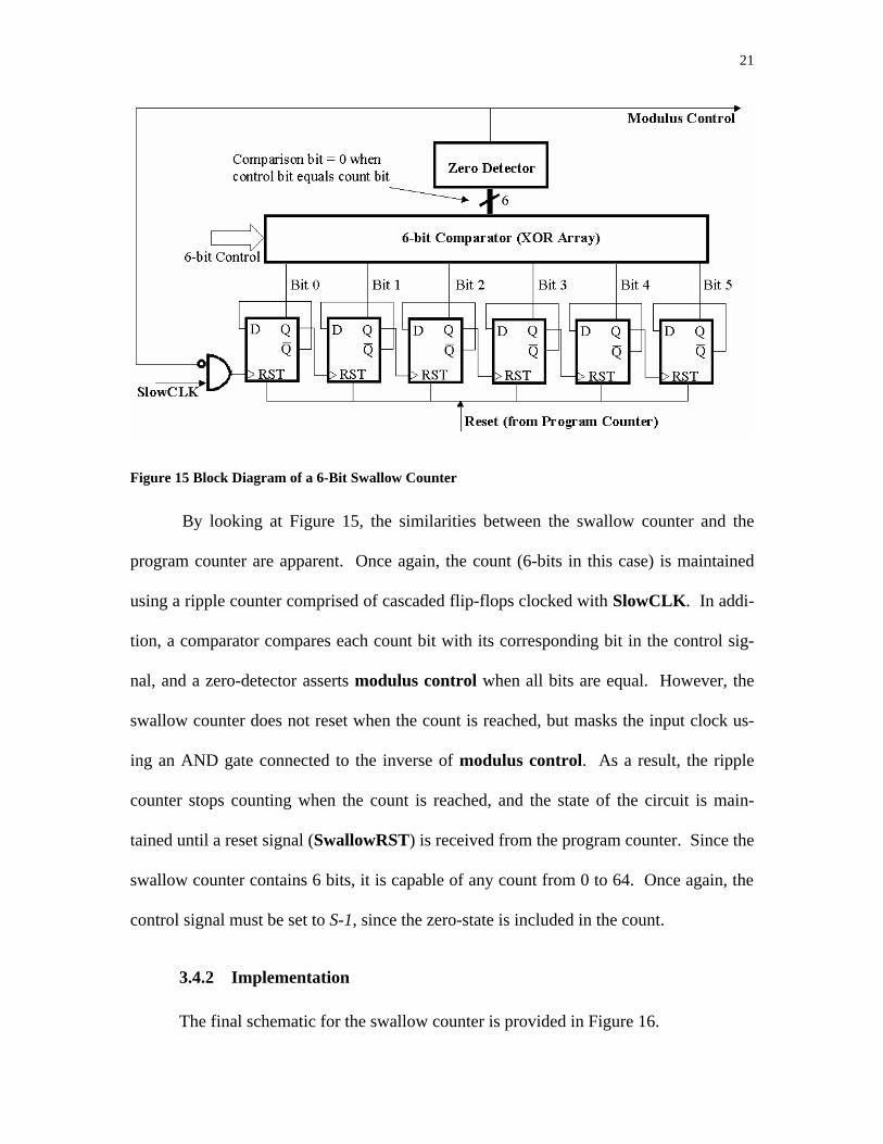
21
Figure 15 Block Diagram of a 6-Bit Swallow Counter
By looking at Figure 15, the similarities between the swallow counter and the
program counter are apparent. Once again, the count (6-bits in this case) is maintained
using a ripple counter comprised of cascaded flip-flops clocked with SlowCLK. In addi-
tion, a comparator compares each count bit with its corresponding bit in the control sig-
nal, and a zero-detector asserts modulus control when all bits are equal. However, the
swallow counter does not reset when the count is reached, but masks the input clock us-
ing an AND gate connected to the inverse of modulus control. As a result, the ripple
counter stops counting when the count is reached, and the state of the circuit is main-
tained until a reset signal (SwallowRST) is received from the program counter. Since the
swallow counter contains 6 bits, it is capable of any count from 0 to 64. Once again, the
control signal must be set to S-1, since the zero-state is included in the count.
3.4.2 Implementation
The final schematic for the swallow counter is provided in Figure 16.

22
Figure 16 Cadence Schematic showing the overall structure of the 6-Bit Swallow Counter
The schematic in Figure 16 shows the 6-bit ripple counter implemented as an ar-
ray of flip-flops, and clocked with the gated clock provided by the AND of SlowCLK
and modulus control. In addition, the comparator is implemented as an array of MCML
XNOR gates, while the zero-detector is actually implemented as a one-detector using a
tree of cascaded AND gates. Unlike the program counter however, no additional cir-
cuitry is necessary to generate the reset as the reset is received from the program counter
by means of the SwallowRST signal.
3.4.3 Simulation Results
Simulation results for the swallow counter, with S set to 20, are provided in Figure
17. The count bits S0-S5 are shown counting upwards in binary on the falling edges of

23
SlowCLK. As expected, modulus control is asserted when the count is reached, and all
signals are held at their current state until the RST signal is received. After RST, the cy-
cle begins again from the beginning. The waveforms in Figure 17 illustrate the success-
ful operation of the swallow counter.
Figure 17 Swallow Counter Simulation Results (S=20)
3.5 Simulation of Frequency Divider
Figure 18 displays the simulation results of the overall frequency divider for an input
frequency of 800 MHz and a division ratio of 800. The input signal is not displayed since
800 MHz appears as a solid bar on this scale. This represents the case when the radio-
over-fiber receiver is receiving signals in the 1.8 GHz band and an 800 MHz local oscil-
lator frequency is required to down-convert the signal to an intermediate frequency of
1GHz. The crystal reference frequency is assumed to be 1 MHz, resulting in a required

24
division ratio of 800. This division ratio was achieved by setting S=20 and P=52, re-
membering that the actual binary control signals are programmed with S-1 and P-1.
Figure 18 Frequency Divider Simulation Results (Fin=800MHz, DIV=800)
The output pulses on Fout are separated by a period of 1µs, corresponding to an
output frequency of 1MHz. In addition, the output duty cycle is much less than 50 per-
cent, as the pulses are high for only slightly more than 1 cycle of SlowCLK. This fact
necessitates the use of the duty-cycle independent phase/frequency detector previously
discussed. Figure 18 also indicates the operation of other key signals in the complete cy-
cle of the frequency divider. At the beginning of each cycle, modulus control is low,
and SlowCLK has a frequency that is equal to Fin/16. After some period of time (20
cycles of SlowCLK in this case), the swallow counter asserts modulus control, changing
the modulus of the prescaler to 15. While this frequency difference is difficult to observe
in the waveform, the frequencies of SlowCLK with modulus control low and high were

25
measured and found to be correct. At the end of the cycle (P pulses of SlowCLK), an
output pulse is generated. On the next clock cycle, a spike can be observed on the Swal-
lowRST line, resetting all counts to zero and restarting the division cycle.
The frequency divider was also successfully simulated with an input frequency of
900 MHz and a division ratio of 900. However, the simulation was unsuccessful when
the input frequency was increased to 1.4 GHz with a division ratio of 1400. An investi-
gation into the cause of the failure indicated that although the swallow counter and pro-
gram counter functioned correctly, the dual modulus prescaler did not change its modulus
when modulus control was asserted. This resulted in excessive delays in the next-state
generation circuit that failed to skip the 16th state and divide by 15. Measurements of the
output frequency confirmed that the results were consistent with the case in which the
DMP always divided by 16. With more time, this problem could be fixed by optimizing
the MCML logic gates used in the circuit to operate at a higher frequency.
4 MOS CURRENT MODE LOGIC (MCML)
4.1 Introduction
At the heart of both the phase/frequency detector and the programmable frequency
divider is the digital logic used to implement the designs presented in the last few sec-
tions. The choice of digital logic family has dramatic effects on the maximum frequency
of operation of the devices, as well as on the power consumption of the circuit. Although
most of the circuit operates at speeds of less than 100 MHz, the dual-modulus prescaler is
required to operate at the required local oscillator frequency of up to 1.4GHz. Since this
frequency is generally too high for standard CMOS logic, it was decided to use MOS

26
Current Mode Logic (MCML) for all digital logic components. In addition to its faster
speed, MCML is also differential, which allows for easy interfacing to the differential
voltage-controlled-oscillator (VCO), and which suppresses common-mode noise from
sources such as the power supply. As will be demonstrated later in this section, its im-
plementation also prevents substrate coupling, which can have drastic effects on the per-
formance and reliability of the circuit. This section discusses the basic theory behind
MCML, and outlines the design of the cell library used in the implementation of the fre-
quency synthesizer. For each gate, an overview of the design is presented along with its
schematic and layout, and simulation results are provided together with measurements of
its characteristics.
4.2 Theory
A diagram of an ideal MCML logic gate is presented in Figure 19. As indicated in
the diagram, an MCML logic gate can be sub-divided into three main elements: a current
sink, a pull-down network, and a resistive load. Digital logic is realized by designing the
pull-down network to switch the current completely from one branch of the load to an-
other, based on the combination of the differential input signals. In the branch where cur-
rent is flowing, a resistive voltage drop equal to IR is developed at the output while at the
complementary output, no current flows through the resistor and the output is tied to
VDD. Therefore, the output signal swing is completely determined by the tail current
and the value of the resistive load, where the output high level is VDD, and the low level
is VDD-IR. The increased speed of MCML logic gates compared to standard CMOS re-
sults from the fact that the load capacitance only needs to be charged or discharged by an
amount equal to the signal swing, rather than the full rail-to-rail difference required by

27
CMOS logic. In addition, the absence of full rail-to-rail swings prevents substrate cou-
pling.
Figure 19 Ideal MCML Logic Gate [2]
In general, the propagation delay of the ideal MCML gate is proportional to the
output signal swing by means of the relation:
τp=(C*∆V)/I, (3)
where C is the load capacitance seen by the logic gate [2]. This relationship indicates
that the propagation delay can be reduced by lowering the signal swing, or by increasing
the tail current which is used to charge and discharge the capacitance. It should be noted
however that the current and the signal swing are closely related. If the current is in-
creased, the resistance should be decreased in order to keep the swing constant.
MCML logic also differs from standard CMOS logic in its power consumption.
While standard CMOS logic dissipates power only when switching, MCML logic gates
dissipate a constant power equal to VDD*I [2]. Since the power consumed in standard
CMOS logic is proportional to its frequency of operation, there is a frequency above

28
which MCML gates actually dissipate less power than their CMOS equivalents. How-
ever, for low frequency applications, the static power consumed by MCML can be drasti-
cally worse than standard CMOS. Generally, MCML gates are used for high frequency
applications, or where differential logic is desired, and standard CMOS logic is used for
lower frequency applications. In this project, this boundary frequency occurs around
100MHz. Although most of the circuit operates at frequencies less than 100MHz (with
the exception of the DMP), MCML logic gates were used for the entire circuit to elimi-
nate the need to convert logic from one form to the other, and because of the differential
nature of MCML.
In this project, all logic gates were designed to operate with a VDD of 1.8V, a
signal swing of 300mV, and a tail current of 25µA. This results in a power consumption
of 7.5µW per gate.
4.3 Inverter/Buffer
The schematic for the MCML inverter is presented in Figure 20. The pull-down
network of the inverter was implemented as a standard NMOS differential pair supplied
with a tail current through an NMOS current-sink. The gate of the current sink NMOS is
connected to the control signal RFN, which is generated by connecting RFN to an exter-
nal diode-connected NMOS in a current-mirror configuration. Finally, the resistive load
of the MCML inverter (as introduced in Figure 19), is implemented using two PMOS
transistors, biased in the triode region using the bias voltage RFP. By changing RFP, the
equivalent resistance of the PMOS load can be varied, effectively changing the voltage
swing of the inverter. Except for the PMOS load, all transistors are intended to remain in
saturation.

29
Figure 20 Schematic of an MCML Inverter/Buffer
All transistors in the inverter were sized with the minimum gate length of 180nm.
The width of the NMOS current sink was set to 600nm, the width of the differential pair
transistors were set to 1.08µm, and the width of the PMOS load transistors were chosen
to be 900nm. It was decided to keep all transistors as small as possible to conserve space
in the frequency synthesizer. Since there are many gates used in the overall design, lar-
ger transistors could quickly consume all available space for little performance gain. In
addition, the differential pair transistors were kept small to reduce the input capacitance,
which would be seen by other gates connected to its input. Increasing the size of these
transistors would have the effect of increasing the gain of the device, but could also in-
crease the delay of the logic circuits. Since the primary motivation for using MCML is

30
its speed, the gain of the inverter was sacrificed to reduce the propagation delay. By ex-
perimentation, it was determined that an RFP bias voltage of 900mV and a tail current of
25µA resulted in a signal swing that was close to 300mV. Although a larger current
could be used to reduce delay, the total power consumption in the circuit would grow to
unacceptable levels.
For simplicity, and to ensure that the same bias circuit could be used for all gates
in the frequency synthesizer, the same transistor sizes, bias voltage, and bias current were
used for all MCML logic gates. This also ensures that the signal swing is the same for all
gates in the circuit.
It is interesting to note that since MCML is fully differential, each and every gate
naturally contains the complement of all its signals. As a result, the MCML inverter is
never used to perform a logical inversion, but to buffer and regenerate signals.
The layout of the MCML inverter/buffer is provided in Figure 21. All gates were
designed using the 0.18µm CMOS technology provided by CMC. This process is a sin-
gle poly salicide process with 6 metal layers. The supply voltage used for the process is
1.8V. A standard-cell configuration was used in the layout of all logic gates to facilitate
interconnections in a top-level circuit. Power supply rails such as VDD and ground were
run externally in metal3, and RFN and RFP were run externally in metal4. Locally, sig-
nals were run in metal1 or metal2. This configuration allows the power and bias rails of
logic gates to be connected together, forming one common rail and simplifying the bias
arrangement. The active PMOS load can be seen at the top of the layout in a shared n-
well with a common bulk contact connected to VDD. In addition, one bulk contact was
shared for all NMOS devices in the layout, and can be seen at the bottom of the layout

31
connected to ground. All metal interconnects were kept as wide as possible to reduce re-
sistance, and at least two contacts were used when connecting different metal layers.
Based on the small size of the transistors, it was decided not to finger the devices. Due to
the digital nature of the device, and since all transistors share the same small region of the
chip, process variations are not a major concern. All of the layout principles applied to
the inverter were also used in the layout of the other MCML gates. In fact, all gates used
identical layouts with the exception of the pull-down networks.
The layout was extracted and successfully passed an LVS (layout-vs.-schematic)
scan. Post-layout simulation results are presented in Figure 22. Ideal input signals with a
voltage swing of 300mV were provided to the inputs of the inverter, and the resulting
Out and OutBar signals are displayed. As expected, the logical inverse of the input sig-
nal is seen on OutBar, while Out displays the buffered input signal. These waveforms
confirm the successful post-layout operation of the MCML inverter buffer.

32
Figure 21 Layout of MCML Inverter/Buffer

33
Figure 22 Post-Layout Simulation of the MCML Inverter/Buffer
The propagation delay defined at the 50% signal points, and the rise and fall-times
defined at the 10% and 90% points are provided in Table 1. For the purpose of rise and
fall-times, the inverter was connected to an output load of two inverters to represent the
approximate load capacitance that would be seen by the gate. The results in Table 1 indi-
cate a signal swing of 350mV and rise and fall times that are slightly better for the case of
the post-layout simulation. This was unexpected since parasitics in the extracted layout
usually increase capacitance in the circuit and decrease the speed of the gate.

34
Pre-layout Post-Layout
Output High 1.8 V 1.8 V
Output Low 1.45 V 1.45 V
Prop. Delay 160 ps 146 ps
Rise Time 121 ps 113 ps
Fall Time 185 ps 164 ps
Table 1 Inverter/Buffer Performance Measurements
4.4 OR/NOR
The schematic for the OR/NOR gate is indicated in Figure 23. As previously dis-
cussed, all transistors use the same sizing scheme as the inverter, and the PMOS load and
current-sink circuitry are identical. However, the pull-down network now contains two
levels to allow for the two differential inputs, A and B. Since each level of logic must
drop a certain proportion of the overall voltage to remain in saturation, only two-input
logic gates were implemented. Further inputs would require additional layers in the pull-
down network, making it difficult to keep all transistors in saturation and limiting the
output voltage swing.

35
Figure 23 Schematic of an MCML OR/NOR Gate
Using the same layout principles discussed for the inverter, a layout was created
for the OR/NOR gate. The final layout is displayed in Figure 24. The standard cell con-
figuration is clearly evident in Figure 24, as is the NMOS current-sink and the active
PMOS load. As expected, only the pull-down network was re-designed. The layout was
extracted and successfully passed an LVS scan. Post-layout simulation results can be
seen in Figure 25.
As desired, Out is high when either of the two signals is high, successfully im-
plementing the OR function. The inverse, OutBar, successfully demonstrates the result
of a NOR operation. Interestingly, parasitics in the extracted OR gate result in “glitches”
in the OutBar signal on the falling edges of A.

36
Figure 24 Layout of the MCML OR/NOR Gate
Figure 25 Post-layout Simulation Results for the MCML OR/NOR

37
The propagation delay defined at the 50% signal points, and the rise and fall-times
defined at the 10% and 90% points are provided in Table 2. For the purpose of rise and
fall-times, the OR gate was connected to an output load of two inverters to represent the
approximate load capacitance that would be seen by the gate. The results in Table 2 indi-
cate a signal swing of 300mV and rise and fall times that are slightly better for the case of
the post-layout simulation. This was unexpected since parasitics in the extracted layout
usually increase capacitance in the circuit and decrease the speed of the gate.
Pre-layout Post-Layout
Output High 1.8 V 1.8 V
Output Low 1.5 V 1.5 V
Prop. Delay 58 ps 53 ps
Rise Time 134 ps 123 ps
Fall Time 229 ps 218 ps
Table 2 OR/NOR Performance Measurements
4.5 AND/NAND
The schematic for the MCML AND/NAND gate is provided in Figure 26. Interest-
ingly, the topology of the AND/NAND gate is identical to that of the OR/NOR. As a re-
sult, the gates are distinguished only by the labels provided to the inputs and outputs.

38
Figure 26 Schematic of an MCML AND/NAND Gate
The layout for the AND/NAND gate is provided in Figure 27. As in the case of
the schematic, it is identical to the OR/NOR except for the labeling of the inputs and out-
puts. The layout successfully passed an LVS scan. Post-layout simulation results for the
AND gate are provided in Figure 28. Since Out is high only when both A and B are
high, Figure 28 confirms the successful operation of the AND function. Once again, the
NAND function is realized using the OutBar signal.
Since the layout of the AND/NAND gate is identical to that of the OR/NOR gate,
its performance metrics are also identical. They are presented in Table 3 for the sake of
completeness.

39
Figure 27 Layout of an MCML AND/NAND Gate
Figure 28 Post-layout Simulation Results of the AND/NAND Gate

40
Pre-layout Post-Layout
Output High 1.8 V 1.8 V
Output Low 1.5 V 1.5 V
Prop. Delay 58 ps 53 ps
Rise Time 134 ps 123 ps
Fall Time 229 ps 218 ps
Table 3 AND/NAND Performance Results
4.6 XOR/XNOR
Figure 29 shows the schematic of an MCML XOR/XNOR gate. Although it is
much more complicated than the gates already presented, symmetry is still evident in the
circuit. This is desirable since asymmetry can result in an output voltage swing that is
different for the Out and OutBar signals. Once again, the common PMOS load and
NMOS current-sink is used.
The layout of the XOR/XNOR gate is provided in Figure 30. The standard-cell
configuration is clearly evident, as is the PMOS load and the current-sink. Only the pull-
down network was redesigned to implement the XOR function. The layout successfully
passed an LVS scan. Post-layout simulation results are displayed in Figure 31. From
Figure 31, it is clearly evident that Out is high only when the values of the two input sig-
nals are the same. When the signals match, Out is low, successfully implementing the
XOR function, and forming the basis for its use in the comparators of the program and
swallow counters.
The propagation delay defined at the 50% signal points, and the rise and fall-times
defined at the 10% and 90% points are provided in Table 4. For the purpose of rise and

41
fall-times, the XOR gate was connected to an output load of two inverters to represent the
approximate load capacitance that would be seen by the gate. The results in Table 4 indi-
cate a signal swing of 300mV and rise and fall times that are slightly better for the case of
the post-layout simulation. This was unexpected since parasitics in the extracted layout
usually increase capacitance in the circuit and decrease the speed of the gate.
Figure 29 Schematic of an MCML XOR/XNOR Gate
Pre-layout Post-Layout
Output High 1.8 V 1.8 V
Output Low 1.5 V 1.5 V
Prop. Delay 72 ps 63 ps
Rise Time 153 ps 139 ps
Fall Time 278 ps 253 ps
Table 4 XOR/XNOR Performance Measurements

42
Figure 30 Layout of an MCML XOR/XNOR Gate
Figure 31 Post-layout Simulation Results for the XOR/XNOR

43
4.7 D-Latch
The schematic of the MCML D-Latch is provided in Figure 32. Once again, the
key elements of all MCML gates are present including the PMOS load, NMOS current
sink, and pull-down network. All transistor sizes and bias voltages are consistent with all
other gates in the library. However, in order to implement the asynchronous reset func-
tion, a third level in the pull-down network was required. Unfortunately, the required
topology is asymmetric, resulting in an output voltage swing that is larger for Out
(350mV) than for OutBar (300mV). This asymmetry can pose difficulties when inter-
facing the output of the latch to other gates. This problem can be alleviated by passing
the signal through a regenerating buffer to regain the required symmetry.
Figure 32 Schematic of an MCML D-Latch (with Reset)

44
The layout of the MCML D-Latch is shown in Figure 33. In addition to the stan-
dard elements of the layout, extra metal1 lines allow for a greater number of NMOS bulk
contacts for the transistors near the top of the pull-down network. All other layout prin-
ciples are the same as discussed for previous gates. The layout successfully passed an
LVS scan. Post-layout simulation results are displayed in Figure 34. As desired, the D-
input is passed to the output when CLK is high, and Out is latched on the previous value
of D when CLK is low. In addition, the successful operation of RST is demonstrated.
This simulation confirms the successful operation of the D-Latch. Timing values are not
given in this section since the D-Latch is used only within the structure of the D-Flip-
flop. As a result, timing values are presented in the next section for the flip-flop as a
whole.
Figure 33 Layout of an MCML D-Latch (with Reset)

45
Figure 34 Post-layout Simulation Results of the MCML D-Latch
4.8 D-Flip-flop
The MCML D-Flip-flop is arguably the most important logic element in the fre-
quency synthesizer since its operation forms the basis for the edge-detection of the
phase/frequency detector, and for the frequency division and pulse counting in the fre-
quency divider. This section presents two separate implementations of D-Flip-flops. The
first implementation is designed specifically for use in the phase/frequency detector,
while the second implementation is the “work-horse” of the programmable frequency di-
vider.
As shown in Figure 4 (section 2.2), the phase/frequency detector detects edges in
the two input signals by connecting them to the clock inputs of two flip-flops. These flip-
flops have their D inputs permanently connected high, and require an asynchronous reset

46
signal for the proper operation of the circuit. Figure 35 shows the rising-edge sensitive,
resettable D-flip-flop used in the phase/frequency detector. Since the D-input is logically
connected high, it was possible to remove the input and incorporate the logic into the cir-
cuit. The resulting flip-flop, initially suggested by Razavi in [3], is comprised of a series
of cross-coupled OR gates. Simulation results are not presented in this section since the
implementation of phase/frequency detector directly demonstrates its successful opera-
tion.
Figure 35 Schematic of the Phase/Frequency Detector D-Flip-flop
A more general D-flip-flop, used in the frequency divider, is presented in Figure

47
36. It was constructed using two MCML latches in a master-slave configuration. Since
the clock to the second latch is inverted, the flip-flop is falling-edge sensitive, as required
for the successful operation of the ripple counter. In addition, an MCML buffer is used to
regenerate the asymmetric output signal from the latches.
Figure 36 Schematic of a General D-Flip-flop
Simulation results for the flip-flop, using the post-layout implementation of all
MCML logic gates, is provided in Figure 37. As desired, the D input is sampled on the
falling-edge of CLK and is output on Out and OutBar. In addition, Figure 37 demon-
strates the successful reset of the flip-flop during the RST pulse. These results confirm
the successful design and simulation of the flip-flop.
The propagation delay defined at the 50% signal points, and the rise and fall-times
defined at the 10% and 90% points are provided in Table 5. For the purpose of rise and
fall-times, the flip-flop was connected to an output load of two inverters to represent the
approximate load capacitance that would be seen by the gate. The results in Table 5 indi-

48
cate a signal swing of 350mV and rise and fall times that are slightly better for the case of
the post-layout simulation. This was unexpected since parasitics in the extracted layout
usually increase capacitance in the circuit and decrease the speed of the gate.
Figure 37 Post-layout Simulation Results of the MCML D-Flip-flop
Pre-layout Post-Layout
Output High 1.8 V 1.8 V
Output Low 1.45 V 1.45 V
Prop. Delay 210 ps 196 ps
Rise Time 204 ps 190 ps
Fall Time 344 ps 318 ps
Table 5 D-Flip-flop Performance Measurements

49
5 RECOMMENDATIONS
Although the majority of the design met all required specifications, there are many
improvements that could be made if time were available. Firstly, since the frequency
synthesizer was unable to operate at 1.4 GHz, work should be done to optimize the
MCML logic gates presented in the previous section. Early indications suggest that op-
timization could increase the effective speed of the MCML gates to approximately 10
GHz.
Power consumption could also be improved in future implementations of the fre-
quency synthesizer. In the current implementation, MCML logic gates were used for the
entire circuit, regardless of the local frequency of operation. However, as discussed in
section 4.2, MCML consumes much more power than standard CMOS logic at low fre-
quencies. Therefore, future designs could use MCML only where needed and convert to
other logic families for the low frequency components of the circuit.
In addition, ripple counters are often unreliable since transitional states exist as the
count is changing. Although no problems were observed in simulation, some scenarios
could potentially exist where one of these transitional count values in the program
counter or the swallow counter match the control word. Under these circumstances, a
false pulse could be generated by the frequency divider, and the circuit could be reset
prematurely. Further investigation is needed to determine another architecture for the
counter.
Finally, more work should be done to characterize the phase/frequency detector. In
particular, the dead zone described earlier in this report should be measured, and an ap-
propriate delay should be added to the reset path to compensate.

50
6 CONCLUSIONS
Overall, the design of the frequency detector was successful. The phase/frequency
detector and programmable frequency divider were successfully implemented using a
custom-designed library of MCML logic gates. Schematics and layouts were designed
for each MCML gate, and simulation results showed the successful operation of the re-
quired logic functions.
With the exception of operation at 1.4 GHz, all required specifications were met.
This problem can be easily remedied using the optimization of the MCML logic gates
and does not pose a major problem to the future development of the frequency synthe-
sizer.
51
7 REFERENCES
[1] “Telecommunications Circuits”, class notes for 97.455A, Department of
Electronics, Carleton University at Ottawa, Fall 2002
[2] Musicer, Jason, “An Analysis of MOS Current Mode Logic for Low Power and
High Performance Digital Logic”, Department of Electrical Engineering and Computer
Sciences, University of California at Berkeley.
[3] B. Razavi, RF Microelectronics, Upper Saddle River: Prentice Hall, Inc., 1998.
[4] A.S. Sedra and K.C. Smith, Microelectronic Circuits, Oxford: Oxford University
Press, 1998.