a fault-tolerant control strategy for three-level neutral
TRANSCRIPT

University of Wisconsin Milwaukee University of Wisconsin Milwaukee
UWM Digital Commons UWM Digital Commons
Theses and Dissertations
August 2019
A Fault-Tolerant Control Strategy for Three-level Neutral-Point A Fault-Tolerant Control Strategy for Three-level Neutral-Point
Clamped (NPC) Inverter Clamped (NPC) Inverter
Weijun Zhu University of Wisconsin-Milwaukee
Follow this and additional works at: https://dc.uwm.edu/etd
Part of the Electrical and Electronics Commons
Recommended Citation Recommended Citation Zhu, Weijun, "A Fault-Tolerant Control Strategy for Three-level Neutral-Point Clamped (NPC) Inverter" (2019). Theses and Dissertations. 2277. https://dc.uwm.edu/etd/2277
This Thesis is brought to you for free and open access by UWM Digital Commons. It has been accepted for inclusion in Theses and Dissertations by an authorized administrator of UWM Digital Commons. For more information, please contact [email protected].
A FAULT-TOLERANT CONTROL STRATEGY FOR THREE-LEVEL NEUTRAL-POINT
CLAMPED (NPC) INVERTER
by
Weijun Zhu
A Thesis Submitted in
Partial Fulfillment of the
Requirements for the Degree of
Master of Science
in Engineering
at
The University of Wisconsin-Milwaukee
August 2019
ii
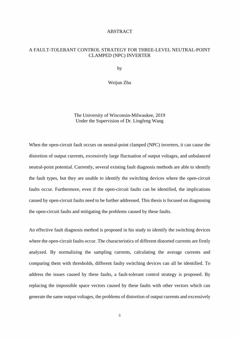
ABSTRACT
A FAULT-TOLERANT CONTROL STRATEGY FOR THREE-LEVEL NEUTRAL-POINT
CLAMPED (NPC) INVERTER
by
Weijun Zhu
The University of Wisconsin-Milwaukee, 2019
Under the Supervision of Dr. Lingfeng Wang
When the open-circuit fault occurs on neutral-point clamped (NPC) inverters, it can cause the
distortion of output currents, excessively large fluctuation of output voltages, and unbalanced
neutral-point potential. Currently, several existing fault diagnosis methods are able to identify
the fault types, but they are unable to identify the switching devices where the open-circuit
faults occur. Furthermore, even if the open-circuit faults can be identified, the implications
caused by open-circuit faults need to be further addressed. This thesis is focused on diagnosing
the open-circuit faults and mitigating the problems caused by these faults.
An effective fault diagnosis method is proposed in his study to identify the switching devices
where the open-circuit faults occur. The characteristics of different distorted currents are firstly
analyzed. By normalizing the sampling currents, calculating the average currents and
comparing them with thresholds, different faulty switching devices can all be identified. To
address the issues caused by these faults, a fault-tolerant control strategy is proposed. By
replacing the impossible space vectors caused by these faults with other vectors which can
generate the same output voltages, the problems of distortion of output currents and excessively

iii
large fluctuation of output voltages can be solved. But the excessively large difference of
neutral-point potential still exists.
To address the above issue, a model predictive control strategy is proposed to solve the problem
of excessively large difference of neutral-point potential. A cost function is built to track the
reference vector and suppress the difference of neutral-point potential. The Lagrange function
is used to solve the action times of different space vectors. Furthermore, it is shown that when
the neutral-point potential is initially unbalanced, the developed strategy is still able to make
the potential balanced and greatly reduce its fluctuation.

iv
© Copyright by Weijun Zhu, 2019
All Rights Reserved

v
TABLE OF CONTENTS
LIST OF FIGURES .............................................................................................................................. vii
LIST OF TABLES ............................................................................................................................... viii
ACKONWLEDGEMENTS ................................................................................................................... ix
Chapter 1 Introduction ............................................................................................................................ 1
1.1Research Background .................................................................................................................... 1
1.2 Multi-Level Topologies ................................................................................................................ 3
1.2.1 NPC Inverter and FC Inverter ................................................................................................ 3
1.2.2 Cascade Multilevel Inverter ................................................................................................... 5
1.2.3 Hybrid Inverter ....................................................................................................................... 6
1.3 Control Strategy ............................................................................................................................ 7
1.3.1 Space Vector Pulse Width Modulation (SVPWM) ................................................................ 7
1.3.2 Fault Diagnosis ...................................................................................................................... 8
1.3.3 Fault Tolerance ...................................................................................................................... 9
1.4 Research Objective and Thesis Layout ......................................................................................... 9
Chapter 2 Principle of Three-Level Inverter ......................................................................................... 11
2.1 Basic Principle ............................................................................................................................ 11
2.2 Switching Sequence .................................................................................................................... 13
2.3 Simulation ................................................................................................................................... 14
2.4 Conclusion .................................................................................................................................. 16
Chapter 3 Fault Diagnosis ..................................................................................................................... 17
3.1 Introduction ................................................................................................................................. 17
3.2 Diagnosis Principle ..................................................................................................................... 17
3.2.1 Type 1 Fault ......................................................................................................................... 17
3.2.2 Type 2 Fault ......................................................................................................................... 20
3.3 Open-circuit Fault Detection Method ......................................................................................... 22
3.3.1 Identification of Faulty Leg ................................................................................................. 22
3.3.2 Classification of the Fault Type ........................................................................................... 22

vi
3.4 Simulation ................................................................................................................................... 25
3.5 Conclusion .................................................................................................................................. 27
Chapter 4 Fault-Tolerant Control Strategy ........................................................................................... 28
4.1 Introduction ................................................................................................................................. 28
4.2 Analysis of Open-Circuit Fault ................................................................................................... 28
4.3 Control Strategy .......................................................................................................................... 28
4.3.1 Fault Occurs to switching tubes ........................................................................................... 28
4.3.2 Fault Occurs to Clamping Diodes ........................................................................................ 31
4.4 Simulation ................................................................................................................................... 34
4.5 Conclusion .................................................................................................................................. 38
Chapter 5 Model Prediction Control Strategy....................................................................................... 39
5.1 Introduction ................................................................................................................................. 39
5.2 Principle ...................................................................................................................................... 39
5.3 Optimization of Cost Function .................................................................................................... 41
5.4 Simulation ................................................................................................................................... 42
5.5 Conclusion .................................................................................................................................. 47
Chapter 6 Conclusion ............................................................................................................................ 48
References ............................................................................................................................................. 50

vii
LIST OF FIGURES
Fig. 1- 1 Infrastructure of smart grid....................................................................................................... 1
Fig. 1- 2 Phase voltage ............................................................................................................................ 2
Fig. 1- 3 line-line voltage ........................................................................................................................ 3
Fig. 1- 4 Inverter topologies: (a) diode clamped inverter; (b) active neutral-point clamped inverter; (c)
T-type inverter; (d) flying-capacitor inverter .......................................................................................... 4
Fig. 1- 5 Phase leg of five-level active neutral-point clamped inverter .................................................. 5
Fig. 1- 6 Cascaded multilevel inverter: (a) cascaded H-Bridge inverter; (b) asymmetric cascaded
inverter; (c) Modular multilevel inverter ................................................................................................ 6
Fig. 1- 7 Hybrid inverter: (a) NPC+CHB; (b) cascaded NPC; (c) ANPC+FC ....................................... 7
Fig. 1- 8 Space vector hexagon for multilevel: (a) three-level; (b) five-level; (c) eleven-level ............. 8
Fig. 2- 1 topology of three-level neutral-point clamped inverter .......................................................... 11
Fig. 2- 2 Distribution of space vectors .................................................................................................. 13
Fig. 2- 3 Simulation for three-level NPC inverter: (a) phase currents; (b) phase voltages; (c) total
harmonic distortion ............................................................................................................................... 16
Table 3- 1 Fault numbers ...................................................................................................................... 26
Table 4- 1 Simulation specifications ..................................................................................................... 34
Table 5- 1 Simulation specifications ..................................................................................................... 42
Table 5- 2 Simulation specifications ..................................................................................................... 45

viii
LIST OF TABLES
Table 2- 1 Working models ....................................................................................................................................11
Table 2- 2 Switching states .....................................................................................................................................12
Table 2- 3 Switching sequence of sector 1..........................................................................................................14
Table 2- 4 Simulation specifications ....................................................................................................................14
Table 3- 1 Fault numbers ........................................................................................................................................26
Table 4- 1 Simulation specifications ....................................................................................................................34
Table 5- 1 Simulation specifications ....................................................................................................................42
Table 5- 2 Simulation specifications ....................................................................................................................45

ix
ACKONWLEDGEMENTS
Firstly, I appreciate my advisor Prof. Lingfeng Wang for offering me much help throughout
the period of my pursing the MS degree. Without his mentorship and support, I could not have
completed this research and obtained my degree. I also want to appreciate David Yu’s help.
Dr. Yu recommended me to apply for Chancellor’s Graduate Student Award, which meant a
lot to me.
I’m grateful to Dr. Zhaoxi Liu. When I had questions about my research, Dr. Liu always could
give me very useful suggestions. Especially, the idea of chapter 4 came from his help. I also
appreciate Dr. Li Ma for recommending some useful websites to me so that I could search
much information on these websites.
I appreciate Dr. Lingfeng Wang, Dr. David Yu and Dr. Wei Wei for spending time in serving
on my defense committee.
I also appreciate all my friends I met here. They invited me to their party and gave me some
advice on my lives. It really helped me a lot.
Finally, I appreciate my parents and my advisor, Shiying Hou in Chongqing University because
of their support such that I could have the chance to study at UWM.
This work was supported in part by China Scholarship Council award CSC201806050241 and
in part by the National Science Foundation Industry/University Cooperative Research Center
on Grid-connected Advanced Power Electronic Systems (GRAPES) under Award GR-18-06.

1
Chapter 1 Introduction
1.1Research Background
Nowadays, because of energy shortages and environmental crises, human’s demanding for
sustainable and clean energy has promoted the development of renewable energy [1]. Solar
cells, wind power as major renewable energy are widely used in power generation systems [2-
3]. These renewable energy systems have brought about tremendous changes to the
infrastructure of the power grid shown in Fig. 1-1.
On the generation side, power converters can work as the interaction between power generation
and grid; for power transmission and distribution, converters work as the key part of HVDC
power transmission and Flexible AC Transmission Systems; for power consumption, power
converters can work as driving device of conveyer belts, compressors, motors, and so on. Thus,
there is a high need to study converters.
Smart grid
Fig. 1- 1 Infrastructure of smart grid
2
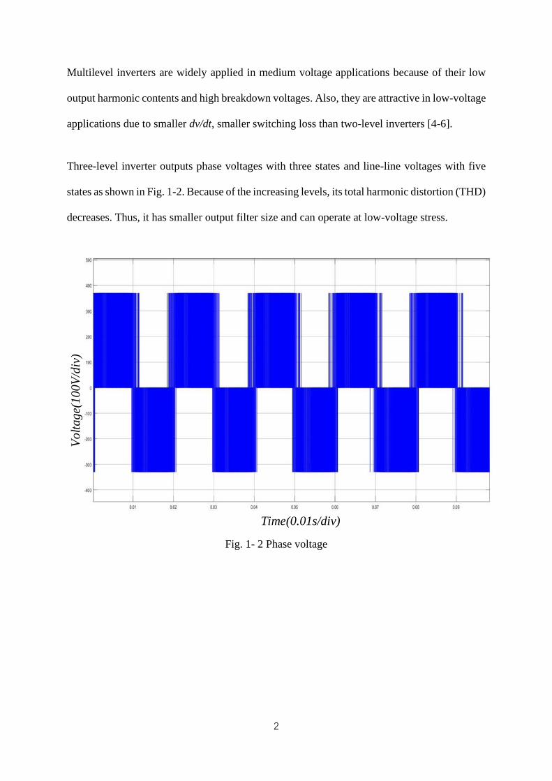
Multilevel inverters are widely applied in medium voltage applications because of their low
output harmonic contents and high breakdown voltages. Also, they are attractive in low-voltage
applications due to smaller dv/dt, smaller switching loss than two-level inverters [4-6].
Three-level inverter outputs phase voltages with three states and line-line voltages with five
states as shown in Fig. 1-2. Because of the increasing levels, its total harmonic distortion (THD)
decreases. Thus, it has smaller output filter size and can operate at low-voltage stress.
Time(0.01s/div)
Volt
age(
100
V/d
iv)
Fig. 1- 2 Phase voltage

3
Time(0.02s/div)
Vo
lta
ge(
200
V/d
iv)
Fig. 1- 3 line-line voltage
1.2 Multi-Level Topologies
In general, multi-level inverter has four kinds of topologies, including Flying-Capacitor (FC)
inverter, Neutral-Point Clamped (NPC) inverter, cascaded multilevel inverter and hybrid
inverter.
1.2.1 NPC Inverter and FC Inverter
NPC inverter and FC inverter have similar characteristics. For NPC inverter, it has three kinds
of topologies, including active inverter, diode clamped inverter and T-type inverter, shown in
Fig. 1-4. A.Nabae proposed three-level diode clamped inverter in 1980 [7]. The two diodes can
be replaced by two active switching tubes and then called active inverter shown in Fig. 1-4(b).
The neutral point and output also can be connected by two switching tubes shown in Fig. 1-
4(c) and named T-type inverter [8-10]. This topology has fewer switching devices and is easily
controlled.
FC inverter has some similar characteristics with diode clamped inverter, such as: topology,

4
control strategy and so on. And it can output voltages with three level through the parallel
capacitor, shown in Fig. 1-4(d).
Even though T-type inverter reduces its switching devices, it increases its voltage stress twice
as much as that of active inverter. When T-type inverter and diode clamped inverter work, the
unbalanced capacitor voltages can increase harmonic distortion of the output currents. Even
though FC inverter doesn’t have such problem, it also needs additional strategies to make the
voltage of the flying capacitor half of that on the DC side.
Fig. 1-5 shows that two-level active inverter is developed into five-level active inverter. The
law of this kind of inverter is generally that 2(𝑘 − 1) switching tubes and (𝑘 − 1)(𝑘 − 2)
diodes are needed to generate 𝑘 levels. It is obvious that the more the levels, the more switching
devices needed and the more complicated the system. Thus, the problem of unbalanced loss is
more serious.
O A O A O A A
(a) (b) (c) (d)
Fig. 1- 4 Inverter topologies: (a) diode clamped inverter; (b) active neutral-point clamped
inverter; (c) T-type inverter; (d) flying-capacitor inverter

5
Fig. 1- 5 Phase leg of five-level active neutral-point clamped inverter
1.2.2 Cascade Multilevel Inverter
Cascade Multilevel Inverter is also widely used. The basic unit of single-phase cascaded
multilevel inverter is a two-level inverter. And with number of basic units increasing, the
number of output levels also increases. So cascaded multilevel inverter is very suitable for high
voltage and high power applications [11].
Fig. 1-6 shows the Cascaded H-Bridge (CHB) multi-level inverter. Each phase has N units and
can generate 2N+1 levels [12]. Fig. 1-6(b) shows asymmetric cascaded inverter whose legs
have different DC voltages. If it has N units, it can generate 2N+1-1 levels. But because of these
different parallel voltages, different switching devices have different voltage stress. Fig. 1-6(c)
shows the modular multilevel with two legs on each phase and it can generate 2𝑁 − 1 levels.

6
Vdc
Vdc
Vdc
4Vdc
2Vdc
Vdc
A
(a) (b) (c)
Fig. 1- 6 Cascaded multilevel inverter: (a) cascaded H-Bridge inverter; (b) asymmetric
cascaded inverter; (c) Modular multilevel inverter
1.2.3 Hybrid Inverter
Hybrid inverter is designed by combining inverter topologies mentioned above. Fig. 1-7(a)
shows the topology combined by NPC topology and CHB topology. The power for NPC part
is supplied by DC source and the power for CHB part is supplied by the capacitor. The more
CHB units, the more levels generated. Because of the NPC units, the problem of unbalanced
neutral-point potential also exists.
Fig. 1-7(b) shows cascaded NPC-H bridge inverter. Each NPC unit in the topology can generate
five levels. The inverter can generate much more levels with very small amounts of basic units
[13-14]. But it also has the problem of unbalanced neutral-point potential because it has NPC
units.
Fig. 1-7(c) shows the hybrid topology combined by ANPC topology and FC topology [15].
This inverter has the advantages of less complicated topology structure and amounts of
switching devices. It can generate 5 levels with 12 switching tubes and 3 capacitors needed.

7
However, for this topology, the loss and voltage stress are extremely unbalanced.
O A
O A
A
(a) (b) (c)
Fig. 1- 7 Hybrid inverter: (a) NPC+CHB; (b) cascaded NPC; (c) ANPC+FC
1.3 Control Strategy
The control strategies play an important role in determining the performance of inverters. Here
show the main control strategies, including space vector pulse width modulation, fault tolerant
control strategy and model prediction control strategy.
1.3.1 Space Vector Pulse Width Modulation (SVPWM)
SVPWM is widely used among multilevel inverters as it can decrease its total harmonic
distortion [16-27]. For three-level inverter, it has 27 voltage space vectors shown in Fig. 1-8(a).
Fig. (c) and (b) show the voltage space vector distribution of five-level inverter and eleven-
level inverter respectively. The switching states are three times of the voltage levels. The higher
levels cause the difficulty in calculating the action times of those voltage space vectors. But
the space vector control strategy is very suitable to three-level inverter because of its simple

8
topology structure and small amounts of vectors.
POO
ONN
PPO
OON
OPO
NON
OPP
NOO
OOP
NNO
POP
ONO
PON
PNN
PPNOPNNPN
NPO
NPP
NOP
NNPONP PNP
PNO
V
I
II
III
IV VI
(a) (b) (c)
Fig. 1- 8 Space vector hexagon for multilevel: (a) three-level; (b) five-level; (c) eleven-level
1.3.2 Fault Diagnosis
The open-circuit fault can cause serious damage to inverters as it can not only reduce
performance of inverters, but also lead to distortion of the output currents and unbalanced
neutral-point potential. So, it is important to study the fault diagnosis strategy.
A lot of scholars have proposed some fault diagnosis method, some of which detect whether
fault occurs by analyzing the output currents [28-32]. Because of the output current with
distortion when open-circuit fault occurs. These current methods include Park’s
transformation, average current and so on.
[33] applies current vector to do the fault detection and fault diagnosis. But for NPC inverter
which has two switching tubes and one diode on upper and lower leg respectively, it can just
identify faulty part, but can’t identify to which device the fault occurs.
[34] uses slope method to identify the faulty switch because different faulty switches have
different characteristics. But this method is only suitable to inverters in the power generation
side and cannot detect faults in the grid side.

9
In [35], current sensors are needed to detect the faulty switch, which is achieved by measuring
the currents and comparing them with normal currents.
1.3.3 Fault Tolerance
In [36], replacing switching states with others is applied to solve faulty states. When open-
circuit fault occurs, one switching state and some voltage space vectors can’t be generated. But
when modulation ratio is small enough, some impossible small voltage space vectors can be
replaced by the others which can generate the same output voltages. But when modulation ratio
become larger and medium vectors are involved into vector composition, this method can’t
work because each sector has only one medium vector which generates certain voltage and
can’t be replaced by others.
In [37] [38] [39] [40], more switching devices are needed to replace the faulty device. If open-
circuit fault occurs, the system can detect the faulty leg and make it isolated and replaced by
other leg. But all these methods need more switching devices.
1.4 Research Objective and Thesis Layout
This thesis clarifies research on three-level neutral-point clamped (NPC) inverter because of
its widely application and high cost-effective. Some methods are proposed to solve the
problems of three-level NPC inverter, which includes unbalanced neutral point potential, fault
diagnosis and fault tolerance control strategy. The chapters in this thesis are organized as
follows:
Chapter 1: Research background and objective are introduced. It is necessary to do research on
inverters because more and more renewable energy needs inverters to convert power. Some
multilevel inverter topologies and control strategies are also introduced.

10
Chapter 2: The basic principle of NPC inverter is introduced, which can be the fundamental of
following chapters.
Chapter 3: The characteristics of output currents are detailedly analyzed, when each fault
occurs to the switch on phase A leg. Based on these characteristics, a method for detecting
faulty leg and diagnosing to which switching device the fault occurs is proposed. And it is
simulated for verification.
Chapter 4: A fault-tolerant control strategy is proposed and simulation is carried out to prove
the proposed method.
Chapter 5: A Model Prediction Control strategy is proposed to reduce the difference of neutral-
point potential. One more simulation proves that this method has better capability even though
the NPC inverter is in worse case.

11
Chapter 2 Principle of Three-Level Inverter
2.1 Basic Principle
This chapter introduces the common control strategy, SVPWM which is widely used among
multilevel inverters. The topology of three-level inverter is shown in Fig. 2-1.
1aS
2aS
4aS
3aS
1bS
2bS
4bS
3bS
1cS
2cS
4cS
3cS
dci
ai
bi
ci
1cV
2cV
1C
2C
+
−
+
−
O
N
LA
LB
LC
RA
RB
RC
Vdc
Dca1
Dca2
Dcb1
Dcb2
Dcc1
Dcc1
Da1
Da2
Da3
Da4
Db1
Db2
Db3
Db4
Dc1
Dc2
Dc3
Dc4
Fig. 2- 1 topology of three-level neutral-point clamped inverter
Table 2-1 shows the three working models of three-level NPC inverter.
Table 2- 1 Working models
Model Sk1 Sk2 Sk3 Sk4 Output
voltage
Switching
state
1 1 1 0 0 Vdc/2 P
2 0 1 1 0 0 O
3 0 0 1 1 -Vdc/2 N
Where, k can replace a, b and c; Sk1, Sk2, Sk3 and Sk4 mean switching states of each switching
tubes; 1 means turn-on, 0 means turn-off.
Each phase voltage can be expressed by 𝑆𝑎, 𝑆𝑏 and 𝑆𝑐, shown as follows

12
{
𝑉𝑎 =
𝑉𝑑𝑐
2𝑆𝑎
𝑉𝑏 =𝑉𝑑𝑐
2𝑆𝑏
𝑉𝑐 =𝑉𝑑𝑐
2𝑆𝑐
(2-1)
Where 𝑆𝑘 = { 1 0−1
, k=a, b or c.
Voltage space vector can be defined as:
V =2
3(𝑉𝑎 + 𝑤𝑉𝑏 + 𝑤
2𝑉𝑐) (2-2)
Where w = 𝑒𝑗2𝜋
3 = −1
2+ 𝑗√
3
2, which means that the phase is delayed by 180°.
Because Sa has three states, there are 27 states totally for Sa, Sb and Sc. The distribution of space
vectors is shown in Fig. 2-2. Table2-2 only shows 6 switching states.
Table 2- 2 Switching states
Sa Sb Sc V
-1 -1 -1 0
-1 -1 0 1
3𝑉𝑑𝑐𝑒
−𝑗120°
-1 -1 1 2
3𝑉𝑑𝑐𝑒
−𝑗120°
-1 0 -1 1
3𝑉𝑑𝑐𝑒
−𝑗120°
-1 0 0 1
3𝑉𝑑𝑐𝑒
−𝑗180°
-1 0 1 √3
3𝑉𝑑𝑐𝑒
−𝑗150°

13
POO
ONN
PPO
OON
OPO
NON
OPP
NOO
OOP
NNO
POP
ONO
PON
PNN
PPNOPNNPN
NPO
NPP
NOP
NNPONP PNP
PNO
V
I
II
III
IV VI
1 2 3
4
Fig. 2- 2 Distribution of space vectors
2.2 Switching Sequence
Switching order of the three-level NPC inverter often maintains two steps:
1) In order to avoid the straight-through (four switches connected in series are turned on or off
at the same time), the switching state of the same bridge arm does not allow the P state to
directly switch to the N state.
2) In order to reduce the switching frequency and switching losses of the NPC inverter, the
three-phase bridge arm only allows the state of one phase bridge arm to be converted when the
switching state is switched. For example, the state [PON] cannot be directly converted to the
state [PPO], but can be switched to the state [POP].
Table 2-3 shows the switching sequence in sector 1.

14
Table 2- 3 Switching sequence of sector 1
Interval Switching sequence
1 POO, OOO, OON, ONN, OON, OOO, POO
2 POO, PON, OON, ONN, OON, PON, POO
3 POO, PON, PNN, ONN, PNN, PON, POO
4 PPO, PPN, PON, OON, PON, PPN, PPO
2.3 Simulation
In order to verify the correctness and effectiveness of SVPWM, the simulation model of the
NPC three-level inverter with a RL load is carried out on Matlab/Simulink. The simulation
specifications are shown in Table 2-4.
Table 2- 4 Simulation specifications
Vdc 80V
Capacitor C1, C2 2000𝜇𝐹
Inductors LA, LB, LC 4mH
Resistor RA, RB, RC 10𝛺
Sampling frequency 10kHz
Fig. 2-2(a) and (b) shows the simulation results of phase voltages and currents. There are three
levels in the phase voltage waveforms and no distortion in currents waveforms.
Fig (c) shows the total harmonic distortion is 0.84%.

15
ia ib ic
Time(0.01s/div)
Cu
rren
t(1A
/div
)
(a)
Time(0.01s/div)
Vo
lta
ge(
10
V/d
iv)
Va Vb Vc
(b)

16
(c)
Fig. 2- 3 Simulation for three-level NPC inverter: (a) phase currents; (b) phase voltages; (c)
total harmonic distortion
2.4 Conclusion
In this chapter, the basic principle of three-level NPC inverter is introduced. The following
chapter will clarify some algorithms which are based on the principle.

17
Chapter 3 Fault Diagnosis
3.1 Introduction
When open-circuit faults occur to three-level NPC inverter, the output current waveform
becomes distorted and the performance of inverter is considerably reduced. Thus, it needs to
detect and identify these faults for further process. This chapter introduces a method to
diagnose these faults.
3.2 Diagnosis Principle
In this section, the characteristics of two different kinds of open-circuit faults in phase A are
analyzed. One is that fault occurs to one of the switching tubes (type 1) and another is that fault
occurs to one of clamping diodes (type 2).
3.2.1 Type 1 Fault
1) Open-Circuit Fault in Sa1: To generate switching state [P], Sa1 and Sa2 should be turned on.
And positive currents will pass through these switching devices. While, when Sa1 fault occurs,
another current path is formed, from Dca1 and Sa2. As the output current decreases to 0, these
switches are reversed-biased, shown in Fig. 3-1(a). When the current decreases to 0, When Sal
fault occurs, the switching state [P] can’t work as normal.
2) Open-Circuit Fault in Sa2: To generate switching state [O], Sa2 and Dca2 should be turned on.
And positive currents will pass through these switching devices. In case of switching state [P],
Sa1 and Sa2 should be turned on. And positive currents will pass through these switching
devices. While, when Sa2 fault occurs, another current path is formed, from Da3 and Da4. As the
output current decreases to 0, these switches are reversed-biased due to the positive voltage,
shown in Fig. 3-1(b).

18
3) Open-Circuit Fault in Sa3: To generate switching state [O], Sa3 and Dca2 will be turned on.
And the current path is formed. To generate switching state [N], Sa3 and Sa4 will be turned on.
And the current path is formed. While, when Sa3 fault occurs, another current path is formed,
from Da1 to Da2. As the output current decreases to zero, the two switches are reverse-biased,
shown in Fig. 3-1(c).
4) Open-Circuit Fault in Sa4: To generate switching state [N], Sa3 and Sa4 should be turned on.
And the current path is formed. While, when Sa4 fault occurs, another current path is formed,
from Dca2 to Sa3. As the output current decreases to zero, Dca2 is reverse-biased, shown in Fig.
3-1(d).
ia
ib ic
Time(0.05s/div)
Volt
ag
e(1
0V
/div
)C
urr
ent(
1A
/div
)
Va
(a)

19
ia
ib ic
Time(0.05s/div)
Vo
lta
ge(
10
V/d
iv)
Cu
rren
t(1
A/d
iv)
Va
(b)
ia ib ic
Time(0.05s/div)
Vo
lta
ge(
10
V/d
iv)
Va
Cu
rren
t(1
A/d
iv)
(c)

20
ia ib ic
Time(0.05s/div)
Va
Volt
age(
10V
/div
)C
urr
ent(
1A
/div
)
(d)
Fig. 3- 1 Output phase currents and voltage for faults (a) Sa1 fault; (b) Sa2 fault; (c) Sa3 fault;
(4) Sa4 fault
3.2.2 Type 2 Fault
1) Open-Circuit Fault in Dca1: When the inverter is in normal case, to generate the switching
state [O], the current path is formed, from Dca1 to Sa2. When the fault occurs, another current is
formed, from Da3 to Da4. The overall analysis is almost the same with type-A fault. The output
currents and voltage waveforms are shown in Fig. 3-2(a).
2) Open-Circuit Fault in Dca2: When the inverter is in normal case, to generate the switching
state [O], the current path is formed, from Dca2 to Sa3. When the fault occurs, another path is
formed, from Da1 to Da2. The output currents and voltage waveforms are shown in Fig. 3-2(b).

21
ia ib ic
Time(0.05s/div)
Va
Volt
ag
e(1
0V
/div
)C
urr
ent(
1A
/div
)
(a)
ia ibic
Cu
rren
t(1
A/d
iv)
Volt
ag
e(1
0V
/div
)
Va
(b)
Fig. 3- 2 Output phase currents and voltage for faults: (a) Dca1 fault; (b) Dca2 fault

22
3.3 Open-circuit Fault Detection Method
3.3.1 Identification of Faulty Leg
Iax
Iax_ave(-) Iax_ave(+)
Iax_(all)
Fig. 3- 3 Definition of variables for the fault detection
The average value of positive current of each phase is defined by Ix_ave(+). Similarly, the
average value of negative current is defined by Ix_ave(-). Thus, each phase has two current
values. In this thesis, the two variables are used to judge the faulty leg.
Phase A is taken as an example. In normal case, because no faults occur and the current
waveforms are not distorted, Iax_ave(+)=Iax_ave(-) or Iax_ave(+)-Iax_ave(-)=0. When fault
occurs to Sa1, Iax_ave(all)=Iax_ave(+)+Iax_ave(-) has a negative value, shown in Fig. 3-1(a).
And 𝐼𝑎𝑥𝑎𝑣𝑒(𝑎𝑙𝑙) = −(𝐼𝑏𝑥𝑎𝑣𝑒(𝑎𝑙𝑙) + 𝐼𝑐𝑥𝑎𝑣𝑒(𝑎𝑙𝑙)) < 0. Thus, it can be used to judge the faulty
leg by calculating average values of these currents. When open-circuit fault occurs in other
phases, it can be judged by the similar way.
3.3.2 Classification of the Fault Type
Phase A is taken as an example. A method to identify faulty switch is proposed according to

23
the characteristics of currents in the thesis.
As the magnitude of currents change when the load changes. It is necessary to normalize the
current for classification. The phase currents can be normalized as follows:
Imax=max{Ia[1], Ia[2], …Ia[n], Ib[1],…Ib[n],…Ic[1], Ic[2],…Ic[n]} (3-1)
Where, Ia[n] is the sampling current of phase A in the Nth sampling cycle, Ib[n] is the sampling
current of phase B in Nth sampling cycle, Ic[n] is the sampling current of phase C in Nth
sampling cycle; Imax is the maximum sample value.
Once Imax is identified, Ia’[1]=Ia[1]/Imax, Ia’[2]=Ia[2]/Imax,….
In normal case, no faults occur, Ia’[1]+…+Ia’[n]=0, Ib’[1]+…+Ib’[n]=0,
Ic’[1]+…+Ic’[n]=0. But, when faults occurs in phase A, Ia’[1]+…+Ia’[n]≠0 because of the
distorted waveforms. Especially, when fault occurs to Sa1, Ia’[1]+Ia’[2]+…+Ia’[k]<│
Ia’[k+1]+…+Ia’[n] │.
Where, 1…k, mean sample value of upper part of current; k+1,…,n, mean sample value of
lower part of current.
Iax_ave(+)=(Ia’[1]+…Ia’[k])/k (3-2)
Iax_ave(-)=(Ia’[k+1]+…+Ia’[n])/k (3-3)
As is shown in Fig. 3-1 and 3-2, when the fault occurs to Sa1, Sa2 or Dca1, the magnitude of
Iax_ave(+) is smaller than that of Iax_ave(-). When the fault occurs to Sa3, Sa4 or Dca2, the
magnitude of Iax_ave(-) is smaller. Therefore, comparing the magnitude of Iax_ave(+) and
Iax_ave(-) can identify if the fault is in the upper part(Sa1, Sa2 or Dca1) or lower part(Sa3, Sa4 or

24
Dca2).
Because the fault occurring in upper part has similar characteristics with that in lower part.
Faults in upper part are mainly analyzed. According to the characteristic of distortion,
Iax_ave3(+)>Iax_ave1(+)>Iax_ave2(+) (3-4)
Where Iax_ave1(+), Iax_ave2(+) and Iax_ave3(+) represent average value of upper distorted
current for Sa1 fault, Sa2 fault and Dca1 fault respectively.
To judge these three faults, two thresholds are applied as follows:
Iax_ave3(+)>Ithreshold1>Iax_ave1(+)>Ithreshold2>Iax_ave2(+) (3-5)
If the fault is in lower part, it can be identified by similar way. To better illustrate the algorithm,
the flow chart is shown in Fig. 3-4.

25
Start
Calculation of average
values of phase currents,
Ix_ave(all),Ix_ave(-),
Ix_ave(+)
find the maximum
Ix_ave(all) to identify the
faulty leg
Ix_ave(+)<Ix_ave(-)
Ix_ave(+)>Ithr1&&
Ix_ave(-)<-Ithr1
Ix_ave(+)>Ithr1&&
Ix_ave(-)<-Ithr1
Dca1 fault Dca2 fault
Ix_ave(+)>Ithr2 Ix_ave(-)>-Ithr2
Sa1 fault Sa2 fault Sa3 fault Sa4 fault
Fault
tolerant
control
Fault
tolerant
control
Y N
Y
Y
Y
NN
Y
NN
Fig. 3- 4 Flow chart of proposed fault detection
3.4 Simulation
Since there are four switching tubes and two clamping diodes on each phase leg, it has 18 faults
totally. This thesis uses numbers from 1 to 18 to represent these faults and #0 to represent
normal case as shown in table 3-1.

26
Table 3- 1 Fault numbers
Fault # Switch # Fault # Switch #
1 Sa1 10 Dcb2
2 Sa2 11 Sb3
3 Dca1 12 Sb4
4 Dca2 13 Sc1
5 Sa3 14 Sc2
6 Sa4 15 Dcc1
7 Sb1 16 Dcc2
8 Sb2 17 Sc3
9 Dcb1 18 Sa4
Time(0.05s/div)
Nu
mber
(a)

27
Time(0.05s/div)
Nu
mber
(b)
Fig. 3- 5 Simulation for fault diagno: (a) Sa2 fault; (b) Dcc1fault
Fig 3-5(a) shows simulation when the fault occurs to Sa2 and its value is 2. Fig. 3-5(b) shows
simulation when the fault occurs to Dcc1. The two simulations can show that the algorithm
proposed in this thesis is capable of detecting the open-circuit faults and identifying to which
switching device the open-circuit fault occurs.
3.5 Conclusion
A fault diagnosis algorithm is proposed in this chapter. And simulation can verify the
effectiveness of this method. Even if this method can accurately identify the faulty switching
device, it may need more methods to handle this open-circuit fault and output normal currents.

28
Chapter 4 Fault-Tolerant Control Strategy
4.1 Introduction
In engineering cases, even though the faulty switches can be identified, it still needs some time
to handle these cases. Thus, it is necessary for fault tolerant control strategy to work before
faulty switches are replaced.
4.2 Analysis of Open-Circuit Fault
1)Open-circuit fault Sa1: If the open-circuit fault occurs to switch Sa1, space vectors containing
switching state [P] can’t be generated, such as: [PPO], [PON] and so on. But other switching
states [O] and [N] in leg A can be generated normally.
2) Open-circuit fault Sa2: If the open-circuit fault occurs to switch Sa2, space vectors containing
switching state [P] and [O] can’t be generated, such as: [PPO], [OPN] and so on.While other
switching state [N] in leg A can work normally.
3) Open-circuit fault Dca1: If the open-circuit fault occurs to switch Dca1, space vectors
containing switching state [O] can’t be generated, such as: [ONN], [OPN] and so on. While
other switching state [P] and [N] in leg A can be generated normally.
when the fault occurs to other switching devices, the impossible space vectors can be analyzed
by the same way.
4.3 Control Strategy
4.3.1 Fault Occurs to switching tubes
If the open-circuit fault occurs to switching tubes (Sa1, Sa2, Sa3 or Sa4), the output phase currents
are distorted and neutral-point potential is unbalanced as mentioned in Chapter 3. This is
because the switching states [P] or [N] is impossibly generated. Thus, it is necessary to reduce
modulation ratio to generate currents without distortion.
29
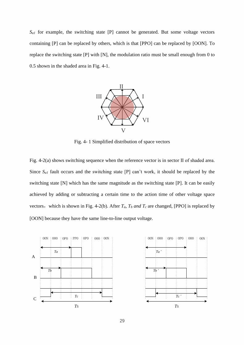
Sa1 for example, the switching state [P] cannot be generated. But some voltage vectors
containing [P] can be replaced by others, which is that [PPO] can be replaced by [OON]. To
replace the switching state [P] with [N], the modulation ratio must be small enough from 0 to
0.5 shown in the shaded area in Fig. 4-1.
Ⅰ
Ⅱ
ⅠⅡ
Ⅳ ⅤⅠ
Ⅴ
Fig. 4- 1 Simplified distribution of space vectors
Fig. 4-2(a) shows switching sequence when the reference vector is in sector Ⅱ of shaded area.
Since Sa1 fault occurs and the switching state [P] can’t work, it should be replaced by the
switching state [N] which has the same magnitude as the switching state [P]. It can be easily
achieved by adding or subtracting a certain time to the action time of other voltage space
vectors,which is shown in Fig. 4-2(b). After Ta, Tb and Tc are changed, [PPO] is replaced by
[OON] because they have the same line-to-line output voltage.
OON OOO OPO PPO OPO OOO OON
Ta
Tb
Tc
OON OOO OPO OPO OOO OON
Ta
Tb
Tc
TSTS
A
B
C
30
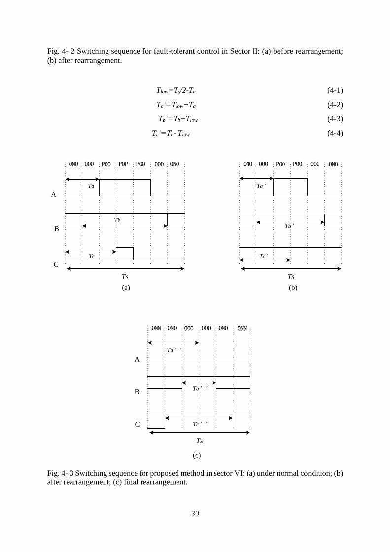
Fig. 4- 2 Switching sequence for fault-tolerant control in Sector Ⅱ: (a) before rearrangement;
(b) after rearrangement.
Tlow=Ts/2-Ta (4-1)
Ta’=Tlow+Ta (4-2)
Tb’=Tb+Tlow (4-3)
Tc’=Tc- Tlow (4-4)
ONO OOO POO POP POO OOO ONO
Ta
Tb
ONO OOO POO POO OOO ONO
Ta
Tb
Tc
TSTS
A
B
C
ONN ONO OOO OOO ONO ONN
Ta
Tb
Tc
TS
A
B
C
(a) (b)
(c)
Tc
Fig. 4- 3 Switching sequence for proposed method in sector Ⅵ: (a) under normal condition; (b)
after rearrangement; (c) final rearrangement.
31
When the reference voltage vector is in sector Ⅵ of shaded area, [PPO] should be replaced by
[OON] because of Sa1 fault, after Tlow is taken to the action time of these voltage vectors as
shown in Fig. 4-3(b). Besides, [POO] also needs to be replaced by [ONN]. The final rearranged
switching sequence is shown in Fig. 4-3(c).
Tlow=Ts/2-Tc (4-5)
Ta’=Ta+Tlow (4-6)
Tb’=Tb-2Tlow (4-7)
Tc’=Tc+Tlow (4-8)
Tlow’=Ts/2-Ta’ (4-9)
Ta’’=Ta’+Tlow (4-10)
Tb’’=Tb’-2Tlow (4-11)
Tc’’=Tc’+Tlow (4-12)
The switching state [P] is replaced by [N], which can cause unbalanced neutral-point potential.
To avoid unbalanced neutral-point potential, the switching state [N] should be replaced by [P]
when the refence vector is in the opposite sector. In case of Sa1 fault, the switching state [P] in
the sectors 1, 2 and 6, is replaced by [N]. Therefore, the switching state [N] in the opposite
sector 3, 4 and 5 should be replaced by [P].
The final rearranged switching sequence is [OPP]-[OOP]-[OOO]-[OOP]-[OPP] in the sectors
4.
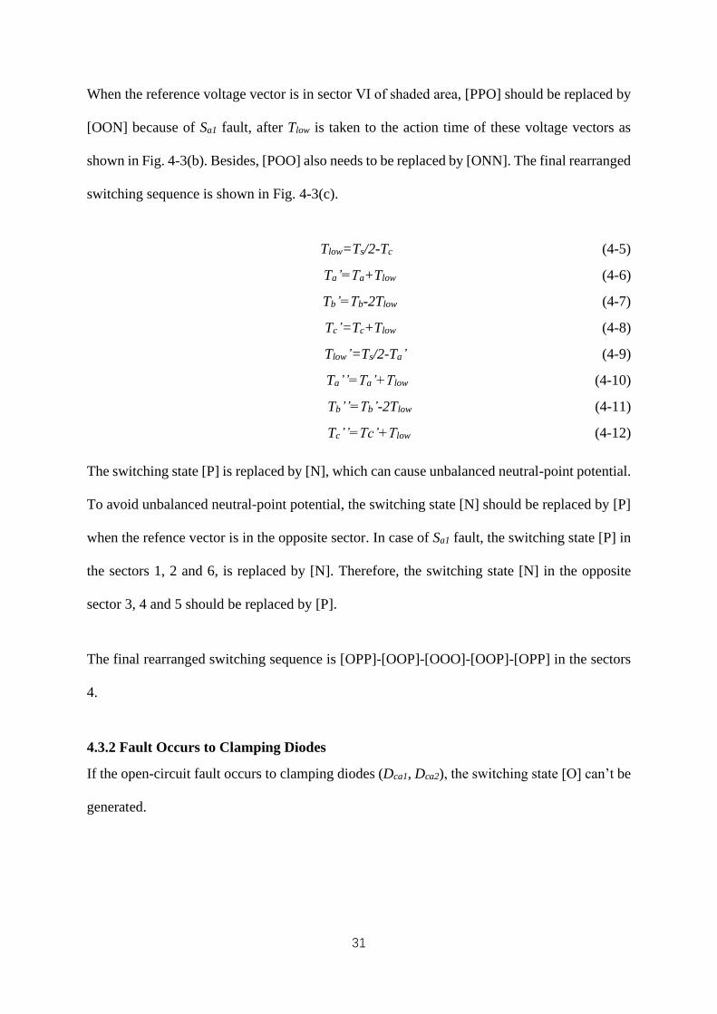
4.3.2 Fault Occurs to Clamping Diodes
If the open-circuit fault occurs to clamping diodes (Dca1, Dca2), the switching state [O] can’t be
generated.
32
PPO PON POO POO PON PPO
TS
A
B
C
PON POO PPO PPO POO PON
TS
A
B
C
Ta =0
Tb
Tc
(a) (b)
Ta=0
Tc
Tb
Fig. 4- 4 Switching sequence for proposed method in sector Ⅰ (shaded area): (a)rearrangement;
(b) final rearrangement.
Ⅰ
Ⅱ
ⅠⅡ
Ⅳ
Ⅴ
ⅤⅠ
Fig. 4- 5 Simplified distribution of space vectors
1)High modulation ratio:If the reference voltage vector is in the shaded area shown in Fig.
4-5, it is impossible to generate the switching state [O] because of Dca1 fault. For example, the
switching sequence should be rearranged as shown in Fig. 4-4(b), after [OON] and [ONN] are
replaced by [PPO] and [POO] respectively as shown in Fig. 4-4(a).
Ta’=0 (4-13)
Tb’= Tb/2 (4-14)
Tc’=TS-Tb+Tc (4-15)
b) Low modulation ratio: Dca1 fault for example, it is impossible to generate voltage vectors

33
containing the switching state [O]. To avoid distortion of output voltage and current, when
[OOO] is replaced by [PPP]. In the opposite area, [OOO] should be replaced by [NNN].
Fig. 4-6(a) shows the switching sequence under normal case. When Dca1 fault occurs, [OOO],
[ONN]and [OON] should be replaced by [PPP], [POO] and [PPO] separately. The rearranged
switching sequence is shown in Fig. 4-6(b). The turn-on times are redefined as follows
Ta’’=TS/2 (4-16)
Tb’= (TS -Tb)/2 (4-17)
Tc’’=(TS -Tc)/2 (4-18)
ONN OON OOO POO OOO OON ONN
Ta
Tb
Tc
OON OOO POO POO OOO OON
Ta
Tb
Tc
TSTS
A
B
C
POO PPO PPP PPP PPO POO
Ta
Tb
Tc
TS
A
B
C
(a) (b)
(c)
Fig. 4- 6 Switching sequence for proposed method (low modulation ratio) in sector Ⅰ: (a) under
normal condition; (b) after rearrangement; (c) final rearrangement.

34
4.4 Simulation
Simulation has been carried out to verify the effectiveness of the proposed fault tolerance
control strategy. The specifications used for the simulation are shown in Table 4-1:
Table 4- 1 Simulation specifications
Vdc 60V
Capacitor C1, C2 470𝜇𝐹
Inductors LA, LB, LC 6mH
Resistor RA, RB, RC 10𝛺
Sampling frequency 10kHz
Vc1
Vc2
Time(0.01s/div)
Vo
lta
ge(
2V
/div
)
(a)

35
Time(0.01s/div)
Volt
age(
10
V/d
iv)
VbVc
(b)
ia ibic
Time(0.01s/div)
Cu
rren
t(0
.5A
/div
)
(c)
Fig. 4- 7 Simulation for proposed fault tolerant control: (a) neutral-point potential; (b) phase
voltages; (c) phase currents.

36
Vc1
Vc2
Time(0.01s/div)
Vo
lta
ge(
10V
/div
)
(a)
ia
ib ic
Time(0.01s/div)
Cu
rren
t(1
A/d
iv)
(b)

37
Time(0.01s/div)
Volt
ag
e(1
0V
/div
)
Vb Vc
Va
(c)
Fig. 4- 8 Simulation for no fault tolerant control strategy: (a) neutral-point potential; (b) phase
currents; (c) phase voltages
It can be seen from the Fig. 4-7(c) and 4-8(b) that the output currents of tolerance control
strategy have better performance and less distortion, compared with that of no control strategy.
From Fig. 4-8(a), it can be seen that the differences between two capacitor voltages become
larger even though they keep balanced state at the beginning. The neutral-point potential in Fig.
4-7(a) has better performance and its fluctuation keeps between 24V and 36 V. And it also can
be seen that the output phase voltages are smoother compared with that of no fault tolerance
strategy shown in Fig. 4-7(b) and 4-8(c). It is caused by the large difference of the neutral-point
potential. In other words, if the neutral-point potential keeps balanced state, the output phase
voltages are smooth and output currents are less distorted.
It can be concluded that with the fault tolerance control strategy, the three-level NPC inverter
has better performance when open-circuit fault occurs.

38
4.5 Conclusion
This chapter introduces the principle of the proposed fault tolerance control strategy and
simulation is used to verify the effectiveness of this strategy. However, the simulation also
shows that though this strategy can improve the performance when the open-circuit fault occurs,
the differences between the two capacitor voltages still exists. In other words, this strategy just
reduces the effect of the open-circuit fault. Thus, it is necessary to propose more effective
method to greatly reduce the difference of two capacitor voltages and further improve the
performance of the inverter.

39
Chapter 5 Model Prediction Control Strategy
5.1 Introduction
Though the difference of the two DC capacitor voltages in chapter 4 is very small, it still affects
the output currents and phase voltages. Thus, this chapter introduce Model Prediction Control
(MPC) strategy to solve this problem.
5.2 Principle
The topology of three-level inverter is shown in Fig. 2-1. To better express the unbalanced
voltage between the two capacitors, two variables are defined as:
{𝑆𝑘ℎ =
𝑆𝑘(𝑆𝑘+1)
2
𝑆𝑘𝑙 =𝑆𝑘(1−𝑆𝑘)
2
(5-1)
Where, 𝑆𝑘 = { 1 0−1
, k=a, b, or c.
According to Kirchhoff's current law,
{𝐶1
𝑑𝑉𝑐1
𝑑𝑡= 𝑖𝑑𝑐 − (𝑆𝑎ℎ𝑖𝑎 + 𝑆𝑏ℎ𝑖𝑏 + 𝑆𝑐ℎ𝑖𝑐)
𝐶2𝑑𝑉𝑐2
𝑑𝑡= 𝑖𝑑𝑐 − (𝑆𝑎𝑙𝑖𝑎 + 𝑆𝑏𝑙𝑖𝑏 + 𝑆𝑐𝑙𝑖𝑐)
(5-2)
Where, 𝐶1 = 𝐶2 = 𝐶; idc, ia, ib, ic are shown in Fig. 2-1.
In discrete system, dx/dt can be expressed by:
𝑑𝑥
𝑑𝑡≈
𝑥(𝑘+1)−𝑥(𝑘)
𝑇𝑠 (5-3)

40
Where x(k+1) is the k+1th sampling value, x(k) is kth sampling value.
Then, equation 5-2 can be expressed by:
{𝑉𝑐1(𝑘 + 1) − 𝑉𝑐1(𝑘) =
𝑇𝑠
𝐶(𝑖𝑑𝑐 − 𝑗ℎ)
𝑉𝑐2(𝑘 + 1) − 𝑉𝑐2(𝑘) =𝑇𝑠
𝐶(𝑖𝑑𝑐 − 𝑗𝑙)
(5-3)
{𝑗ℎ = 𝑆𝑎ℎ𝑖𝑎 + 𝑆𝑏ℎ𝑖𝑏 + 𝑆𝑐ℎ𝑖𝑐𝑗ℎ = 𝑆𝑎ℎ𝑖𝑎 + 𝑆𝑏ℎ𝑖𝑏 + 𝑆𝑐ℎ𝑖𝑐
(5-4)
Equation 5-3 can be simplified by
∆V(k + 1) = ∆V(k) −𝑇𝑆
𝐶(𝑗ℎ − 𝑗𝑙) (5-5)
Where ∆V = 𝑉𝐶1 − 𝑉𝐶2.
When faults occur, only three space vectors work in one cycle. Thus, the difference of capacitor
voltages can be expressed by:
∆V(k + 1) = ∆V(k) − ∑𝑡𝑖
𝐶(𝑗ℎ_𝑖 − 𝑗𝑙_𝑖)
3𝑖=1 (5-6)
Where 𝑗ℎ_𝑖 and 𝑗𝑙_𝑖 are the ith switching states of 𝑗ℎ and 𝑗𝑙 separately.
In this thesis, a cost function is proposed to track the reference voltage and keep neutral-point
potential balanced. The cost function is expressed by:
g = 𝜆1 {[𝑉𝛼𝑟𝑒𝑓(𝑘 + 1)𝑇𝑆 − (𝑉1𝛼𝑡1 + 𝑉2𝛼𝑡2 + 𝑉3𝛼𝑡3)]2
+ [𝑉𝛽𝑟𝑒𝑓(𝑘 + 1)𝑇𝑆 − (𝑉1𝛽𝑡1 + 𝑉2𝛽𝑡2 +
𝑉3𝛽𝑡3)]2
} + 𝜆2(Δ𝑉(𝑘 + 1))2 (5-7)
41
Where, 𝑉𝛼𝑟𝑒𝑓 and 𝑉𝛽𝑟𝑒𝑓 are the horizontal axis components and the vertical axis components of
𝑉𝛼 and 𝑉𝛽 separately in the two-phase stationary coordinate system; λ1and λ2 are the weigh
factor; 𝑉1𝛼, 𝑉1𝛽, 𝑉2𝛼, 𝑉2𝛽, 𝑉3𝛼 and 𝑉3𝛽 are the horizontal axis components and the vertical axis
components of 𝑉1, 𝑉2and 𝑉3 separately which are selected according to nearest three vector
principle. For example, when Sa1 fault occurs, and modulation is small, and the reference
vector is in sector 1, 𝑉1, 𝑉2and 𝑉3 are [OON], [OOO] and [ONN] respectively, based on the
analysis of chapter 4,
5.3 Optimization of Cost Function
To solve the action times of space vectors, Lagrange equation is applied.
Because the cost function is related to t1, t2 and t3, equation 5-7 can be simplified by
{min𝑔(𝑡1, 𝑡2, 𝑡3)
𝑠. 𝑡. 2𝑡1 + 2𝑡2 + 𝑡3 = 𝑇𝑆 (5-8)
Equation 5-8 can be further simplified by
L(𝑡1, 𝑡2, 𝑡3, 𝑡3) = 𝑔(𝑡1, 𝑡2, 𝑡3) + 𝜆(2𝑡1 + 2𝑡2 + 𝑡3 − 𝑇𝑆) (5-9)
Where, 𝜆 is weigh factor, 0 < 𝜆 < 1.
To solve t1, t2 and t3, derivation can be applied to equation 5-9 and expressed by
{
𝑑𝐿
𝑑𝑡1= 0
𝑑𝐿
𝑑𝑡2= 0
𝑑𝐿
𝑑𝑡3= 0
(5-10)
Besides, t1, t2, t3 and t4 all should meet the requirement that
42
{
0 ≤ 𝑡1 ≤ 𝑇𝑆0 ≤ 𝑡2 ≤ 𝑇𝑆0 ≤ 𝑡3 ≤ 𝑇𝑆
(5-11)
Cases where 𝑡1 < 0 may happen according to equation 5-10. Thus, it is necessary to optimize
these action times. If 𝑡1 < 0 occurs, action times can be optimized by
{
t1∗ = 0
t2∗ =
t2
t2+t3+t1
t3∗ =
t3
t2+t3+t1
(5-12)
5.4 Simulation
To verify the effectiveness of the proposed method, simulation on Matlab/Simulink is carried
out. The specifications and parameters used for simulation are shown in table 5-1.
Table 5- 1 Simulation specifications
Vdc 80V
Capacitor C1, C2 470𝜇𝐹
Inductors LA, LB, LC 4mH
Resistor RA, RB, RC 12𝛺
Sampling frequency 10kHz

43
Vc2
Time(0.5s/div)
Volt
age(
1V
/div
)
Vc1
Vc2
(a)
ia ib ic
Time(0.01s/div)
Curr
ent(
0.0
05A
/div
)
(b)

44
Time(0.05s/div)
Volt
ag
e(10
V/d
iv)
Vb Vc
(c)
Fig. 5- 1 Simulation for MPC strategy with balanced neutral-point potential and Sa1 fault: (a)
neutral-point potential; (b) phase currents; (c) phase voltages
It can be seen that the neutral-point potential has smaller fluctuation between 30.1V and 29.9V,
when Sa1 fault occurs. Compared with the result shown in Fig. 4-5 in chapter 4, the proposed
MPC strategy has better performance. The current waveforms in Fig. 5-1(b) show no distortion,
and phase voltages in Fig. 5-1(c) is smooth and has three levels, 0V, 30V and -30V.
In actual engineering environment, the unbalanced load or the different parameters of the
switching devices can cause the unbalanced state of the neutral-point potential. When these
cases occur, they will also considerably reduce the performance of the inverter. To further
verify the effectiveness of the proposed method, another simulation that both unbalanced
neutral-point potential and Sa1 fault occur is carried out. Table 5-2 shows the specifications
and parameters.

45
Table 5- 2 Simulation specifications
Vdc 80V
Vc1 33V
Vc2 27V
Capacitor C1, C2 470𝜇𝐹
Inductors LA, LB, LC 4mH
Resistor RA, RB, RC 10𝛺
Sampling frequency 10kHz
Time(0.5s/div)
Volt
age(
1V
/div
)
Vc1
Vc2
(a)
46
ia ib ic
Time(0.01s/div)
Cu
rren
t(0
.00
5A
/div
)
(b)
Time(0.05s/div)
Volt
ag
e(10
V/d
iv)
Vb Vc
(c)
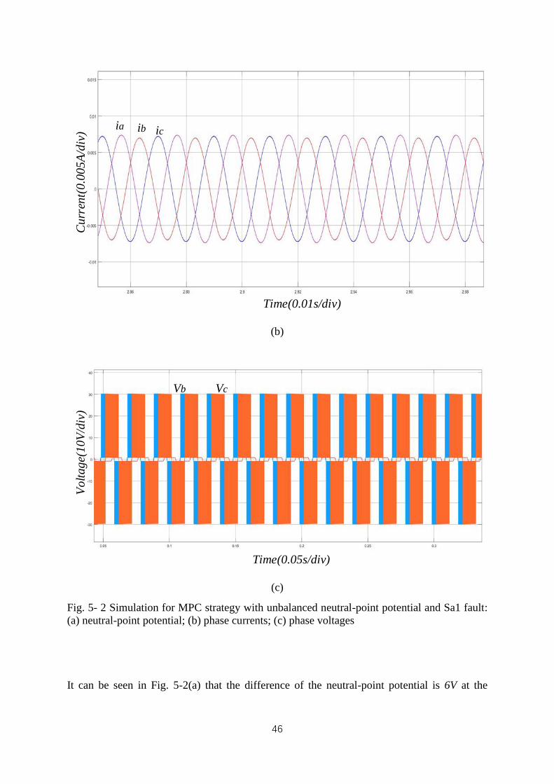
Fig. 5- 2 Simulation for MPC strategy with unbalanced neutral-point potential and Sa1 fault:
(a) neutral-point potential; (b) phase currents; (c) phase voltages
It can be seen in Fig. 5-2(a) that the difference of the neutral-point potential is 6V at the

47
beginning. When the proposed method is added to the system, it takes about 1.2s to make the
neutral-point potential balanced and fluctuate between 30.1V and 29.9V. The current
waveforms and phase voltages also show no distortion even though both Sa1 fault and
unbalanced neutral-point potential occur at the same time.
5.5 Conclusion
This chapter introduces the basic principle of MPC strategy. Simulation for Sa1 fault and
unbalanced neutral-point potential are carried out to verify that the proposed method can
improve the performance of NPC three-level inverter even though inverter is in worse case.
And the simulation also proves that the proposed method can reduce the fluctuation of neutral-
point potential.

48
Chapter 6 Conclusion
This thesis is mainly to introduce the control strategy for NPC three-level inverter to improve
its performance. The main work of this thesis can be concluded as follows:
Firstly, the common principle for NPC three-level inverter is introduced and simulation for the
inverter is carried out to show its performance under normal situation. However, in actual
engineering environment, there are more cases, like open-circuit fault and unbalanced neutral-
point potential.
Secondly, this thesis proposes one method to detect whether faults occurs and identify to which
switching device faults occur. The first step of the proposed method is to detect the faulty leg
based on the characteristic that when one fault occurs, the magnitude of the average value for
the upper part of the output currents is unequal to that of the lower part. According to this, the
faulty leg can be identified. Then, fault occurring to different switching devices will cause
distortion of the output currents and the average value of the distortion is smaller compared
with other parts of the currents. According to this fact, the faulty switching device can be
identified. The simulation verifies that the proposed method can diagnose faults. However, it
is far from enough because in actual engineering environment, before faulty device is replaced,
more measurements should be taken do reduce the loss.
Thirdly, this thesis proposed a fault tolerance control strategy for faulty cases. The faulty
switching device can cause that some voltage space vectors can’t work as usual. While, small
voltage space vectors can be replaced by other small vectors with the same effectiveness. The
replacement of the certain vectors is applied to suppress the negative effect of the faulty
switching device. The simulation also carried out to verify this method.

49
Finally, though the proposed fault tolerance control strategy can suppress the distortion of
output currents, the fluctuation of neutral-point potential is too large. Thus, a Model Prediction
Control strategy is introduced to overcome this drawback. This proposed algorithm is to take
the difference of the neutral-point potential into calculation and accurate action times of space
vectors are used to suppress the too large fluctuation. Besides that, unbalanced neutral-point
potential is added to the faulty case to verify the capacity of this method.

50
References
[1] Oyedepo, S.O. Energ Sustain Soc (2012) 2: 15. https://doi.org/10.1186/2192-0567-2-15
[2] Political power and renewable energy futures: A critical review, Matthew J.Burke, in
Energy Research & Social Science, Vol. 35, pp. 78-93, Jan. 2018.
[3] RENEWABLE ENERGY: A VIABLE CHOICE, By Antonia V. Herzog, Timothy E.
Lipman, Jennifer L. Edwards, and Daniel M. Kammen, Published in Environment, Vol. 43,
no. 10, Dec. 2001.
[4] M. R. J. Oskuee, M. Karimi, S. N. Ravadanegh and G. B. Gharehpetian, “An Innovative
Scheme of Symmetric Multilevel Voltage Source Inverter With Lower Number of Circuit
Devices,” in IEEE Transactions on Industrial Electronics, vol. 62, no. 11, pp. 6965 -6973,
Nov. 2015.
[5] J. I. Leon, S. Kouro, L. G. Franquelo, J. Rodriguez and B. Wu, “The Essential Role and the
Continuous Evolution of Modulation Techniques for Voltage-Source Inverters in the Past,
Present, and Future Power Electronics,” in IEEE Transactions on Industrial Electronics,
vol. 63, no. 5, pp. 2688-2701, May 2016.
[6] J. Rodriguez, Jih-Sheng Lai and Fang Zheng Peng, “Multilevel inverters: a survey of
topologies, controls, and applications,” in IEEE Transactions on Industrial Electronics, vol.
49, no. 4, pp. 724-738, Aug 2002.
[7] A. Nabae, I. Takahashi and H. Akagi, “A New Neutral-Point-Clamped PWM Inverter,”
in IEEE Transactions on Industry Applications, vol. IA-17, no. 5, pp. 518-523, Sept. 1981.
[8] M. Schweizer and J. W. Kolar, "Design and Implementation of a Highly Efficient Three-
Level T-Type Converter for Low-Voltage Applications," in IEEE Transactions on Power
Electronics, vol. 28, no. 2, pp. 899-907, Feb. 2013.
[9] H. Kim, Y. Kwon, S. Chee and S. Sul, "Analysis and Compensation of Inverter
Nonlinearity for Three-Level T-Type Inverters," in IEEE Transactions on Power
Electronics, vol. 32, no. 6, pp. 4970-4980, June 2017.
[10] G. E. Valderrama, G. V. Guzman, E. I. Pool-Mazún, P. R. Martinez-Rodriguez, M. J.
Lopez-Sanchez and J. M. S. Zuñiga, "A Single-Phase Asymmetrical T-Type Five-Level
Transformerless PV Inverter," in IEEE Journal of Emerging and Selected Topics in Power
Electronics, vol. 6, no. 1, pp. 140-150, March 2018.
[11] N. Sujitha, B. Karthika, R. H. Kumar and M. Sasikumar, "Analysis of hybrid PWM
control schemes for cascaded multilevel inverter fed industrial drives," 2014 International
Conference on Circuits, Power and Computing Technologies [ICCPCT-2014], Nagercoil,
2014, pp. 745-750.
[12] C. Kiruthika, T. Ambika and R. Seyezhai, "Implementation of digital control strategy
for asymmetric cascaded multilevel inverter," 2012 International Conference on
Computing, Electronics and Electrical Technologies (ICCEET), Kumaracoil, 2012, pp.
295-300.

51
[13] E. Gurpinar and A. Castellazzi, "Novel multilevel hybrid inverter topology with power
scalability," IECON 2016 - 42nd Annual Conference of the IEEE Industrial Electronics
Society, Florence, 2016, pp. 6516-6521.
[14] C. M. Wu, W. H. Lau and H. Chung, "A five-level neutral-point-clamped H-bridge
PWM inverter with superior harmonics suppression: a theoretical analysis," ISCAS'99.
Proceedings of the 1999 IEEE International Symposium on Circuits and Systems VLSI
(Cat. No.99CH36349), Orlando, FL, 1999, pp. 198-201 vol.5.
[15] P. Barbosa, P. Steimer, J. Steinke, M. Winkelnkemper and N. Celanovic, "Active-
neutral-point-clamped (ANPC) multilevel converter technology," 2005 European
Conference on Power Electronics and Applications, Dresden, 2005, pp.-P.10.
[16] L. Zhang, Y. Fan, R. Cui, R. D. Lorenz and M. Cheng, "Fault-Tolerant Direct Torque
Control of Five-Phase FTFSCW-IPM Motor Based on Analogous Three-Phase SVPWM
for Electric Vehicle Applications," in IEEE Transactions on Vehicular Technology, vol.
67, no. 2, pp. 910-919, Feb. 2018.
[17] S. Pan, J. Pan and Z. Tian, "A Shifted SVPWM Method to Control DC-Link Resonant
Inverters and Its FPGA Realization," in IEEE Transactions on Industrial Electronics, vol.
59, no. 9, pp. 3383-3391, Sept. 2012.
[18] Bor-Ren Lin and Ta-Chang Wei, "Space vector modulation strategy for an eight-switch
three-phase NPC converter," in IEEE Transactions on Aerospace and Electronic Systems,
vol. 40, no. 2, pp. 553-566, April 2004.
[19] Jae Hyeong Seo, Chang Ho Choi and Dong Seok Hyun, "A new simplified space-
vector PWM method for three-level inverters," in IEEE Transactions on Power Electronics,
vol. 16, no. 4, pp. 545-550, July 2001.
[20] Shijie Yan, Qun Zhang and Heng Du, "A simplified SVPWM control strategy for PV
inverter," 2012 24th Chinese Control and Decision Conference (CCDC), Taiyuan, 2012,
pp. 225-229.
[21] D. Zhang, B. Xu, H. Yang and P. Zhu, "Simulation analysis of SVPWM based on
seven-phase permanent magnet synchronous motor," 2017 International Conference on
Control, Automation and Information Sciences (ICCAIS), Chiang Mai, 2017, pp. 251-256.
[22] Z. H. Ali, J. Zhao, E. Manla, J. Ma and W. Song, "Novel direct power control of single-
phase three-level SVPWM inverter for photovoltaic generation," 2017 IEEE Power &
Energy Society Innovative Smart Grid Technologies Conference (ISGT), Washington, DC,
2017, pp. 1-5.
[23] L. Zhai and H. Li, "Modeling and simulating of SVPWM control system of induction
motor in electric vehicle," 2008 IEEE International Conference on Automation and
Logistics, Qingdao, 2008, pp. 2026-2030
[24] Jia YingYing, Wang XuDong, Mao LiangLiang, Yang ShuCai and Zhang HaiXing,
"Application and Simulation of SVPWM in three phase inverter," Proceedings of 2011 6th
International Forum on Strategic Technology, Harbin, Heilongjiang, 2011, pp. 541-544.
[25] R. V. Thomas, Rakesh E, J. Jacob and Chitra A, "Identification of optimal SVPWM

52
technique for diode clamped multilevel inverter based induction motor drive," 2015 IEEE
International Conference on Electrical, Computer and Communication Technologies
(ICECCT), Coimbatore, 2015, pp. 1-6.
[26] Z. Liu, Y. Wang, G. Tan, H. Li and Y. Zhang, "A Novel SVPWM Algorithm for Five-
Level Active Neutral-Point-Clamped Converter," in IEEE Transactions on Power
Electronics, vol. 31, no. 5, pp. 3859-3866, May 2016.
[27] B. Sakthisudhursun, J. K. Pandit and M. V. Aware, "Simplified Three-Level Five-
Phase SVPWM," in IEEE Transactions on Power Electronics, vol. 31, no. 3, pp. 2429-2436,
March 2016.
[28] U. Choi, F. Blaabjerg and K. Lee, "Study and Handling Methods of Power IGBT
Module Failures in Power Electronic Converter Systems," in IEEE Transactions on Power
Electronics, vol. 30, no. 5, pp. 2517-2533, May 2015.
[29] B. Lu and S. K. Sharma, "A Literature Review of IGBT Fault Diagnostic and
Protection Methods for Power Inverters," in IEEE Transactions on Industry Applications,
vol. 45, no. 5, pp. 1770-1777, Sept.-oct. 2009.
[30] J. O. Estima and A. J. Marques Cardoso, "A New Approach for Real-Time Multiple
Open-Circuit Fault Diagnosis in Voltage-Source Inverters," in IEEE Transactions on
Industry Applications, vol. 47, no. 6, pp. 2487-2494, Nov.-Dec. 2011.
[31] J. O. Estima and A. J. Marques Cardoso, "A New Algorithm for Real-Time Multiple
Open-Circuit Fault Diagnosis in Voltage-Fed PWM Motor Drives by the Reference Current
Errors," in IEEE Transactions on Industrial Electronics, vol. 60, no. 8, pp. 3496-3505, Aug.
2013.
[32] U. Choi, J. Lee, F. Blaabjerg and K. Lee, "Open-Circuit Fault Diagnosis and Fault-
Tolerant Control for a Grid-Connected NPC Inverter," in IEEE Transactions on Power
Electronics, vol. 31, no. 10, pp. 7234-7247, Oct. 2016.
[33] M. B. Abadi, A. M. S. Mendes and S. M. A. Cruz, "Three-level NPC inverter fault
diagnosis by the Average Current Park's Vector approach," 2012 XXth International
Conference on Electrical Machines, Marseille, 2012, pp. 1893-1898.
[34] J. Lee, K. Lee and F. Blaabjerg, "Open-Switch Fault Detection Method of a Back-to-
Back Converter Using NPC Topology for Wind Turbine Systems," in IEEE Transactions
on Industry Applications, vol. 51, no. 1, pp. 325-335, Jan.-Feb. 2015.
[35] P. Fazio, G. Maragliano, M. Marchesoni and G. Parodi, "A new fault detection method
for NPC converters," Proceedings of the 2011 14th European Conference on Power
Electronics and Applications, Birmingham, 2011, pp. 1-10.
[36] U. Choi, F. Blaabjerg and K. Lee, "Reliability Improvement of a T-Type Three-Level
Inverter With Fault-Tolerant Control Strategy," in IEEE Transactions on Power
Electronics, vol. 30, no. 5, pp. 2660-2673, May 2015.
[37] S. Yang, D. Xiang, A. Bryant, P. Mawby, L. Ran and P. Tavner, "Condition Monitoring
for Device Reliability in Power Electronic Converters: A Review," in IEEE Transactions
on Power Electronics, vol. 25, no. 11, pp. 2734-2752, Nov. 2010.

53
[38] M. Naidu, S. Gopalakrishnan and T. W. Nehl, "Fault-Tolerant Permanent Magnet
Motor Drive Topologies for Automotive X-By-Wire Systems," in IEEE Transactions on
Industry Applications, vol. 46, no. 2, pp. 841-848, March-April 2010.
[39] W. Wang, M. Cheng, B. Zhang, Y. Zhu and S. Ding, "A Fault-Tolerant Permanent-
Magnet Traction Module for Subway Applications," in IEEE Transactions on Power
Electronics, vol. 29, no. 4, pp. 1646-1658, April 2014.
[40] Y. Song and B. Wang, "Analysis and Experimental Verification of a Fault -Tolerant
HEV Powertrain," in IEEE Transactions on Power Electronics, vol. 28, no. 12, pp. 5854-
5864, Dec. 2013.