a configurable platform for sensor and image …
TRANSCRIPT
The Pennsylvania State University
The Graduate School
The Department of Computer Science and Engineering
A CONFIGURABLE PLATFORM FOR
SENSOR AND IMAGE PROCESSING
A Dissertation in
Computer Science and Engineering
by
Kevin Maurice Irick
2009 Kevin Maurice Irick
Submitted in Partial Fulfillment
of the Requirements
for the Degree of
Doctor of Philosophy
August 2009

The dissertation of Kevin Maurice Irick was reviewed and approved* by the following:
Vijaykrishnan Narayanan
Professor of Computer Science and Engineering
Dissertation Advisor
Chair of Committee
Mary Jane Irwin
Professor of Computer Science and Engineering
Robert E. Noll Professor
Yuan Xie
Associate Professor of Computer Science and Engineering
Vittaldas Prabhu
Professor of Industrial Engineering
Mahmut Kandemir
Professor of Computer Science and Engineering
Graduate Officer for the Department of Computer Science and Engineering
*Signatures are on file in the Graduate School

iii
ABSTRACT
Smart Environments are environments that exhibit ambient intelligence to those that
interact with them. Smart Environments represent the next generation of pervasive computing
enabled by the proliferation of low cost, high performance, embedded devices. The enabling
technology behind this new paradigm of pervasive computing is the Smart Sensor. A Smart
Sensor is a device that combines physical sensing apparatus with a computational entity that
allows localized interpretation of sensor data. In time critical applications the interpretation of
the data can result in an immediate process decision such as alerting mine occupants of the
rapidly decreasing quantity of oxygen in a corridor. In less time sensitive applications, such as
shopper behavior analysis, a Smart Camera can analyze the behavior of retail store patrons
captured by an onboard CMOS camera and send statistics to the store manager periodically or by
request.
Advances in semiconductor manufacturing technologies have resulted in extremely small
transistor feature sizes, low operating voltages, and increased operating frequencies. Overall,
embedded semiconductor devices have experienced increasing computational power in
decreasing package sizes. In addition, sensor technology has seen advancements that yield more
reliable, accurate, and smaller sensors that are easier to interface. Advanced research in polymer
nanowires has resulted in the development of gas sensors, consisting of nanowire arrays
assembled on CMOS wafers that can detect the presence of volatile compounds at extremely low
concentrations. Moreover, CCD imaging sensors are rapidly being replaced by cheaper, lower
power consuming, faster, and higher resolution CMOS alternatives.
Consequently, the case for Smart Sensor utility has been proven by numerous and diverse
application scenarios. What‟s left is the development of novel computational architectures that
implement the intelligence for a wide range of Smart Sensing applications while adhering to tight

iv
footprint constraints, strict performance requirements, and green power profiles. Issues in
hardware acceleration, algorithm mapping, low power design, networking, and hardware/software
co-design are all prevalent in this new embedded system paradigm. Of particular interest, and
consequently the focus of this dissertation, are reconfigurable architectures that can be tuned to
leverage the appropriate amount of computational resources to meet the performance
requirements and power budget of a particular application. Specifically, this dissertation
contributes novel hardware architectures for gas sensing, face detection, and gender recognition
algorithms that are suitable for deployment on FPGAs. Further, this dissertation contributes an
FPGA programming framework that reduces the complexities associated with the design of
reconfigurable hardware systems.

v
TABLE OF CONTENTS
LIST OF FIGURES ................................................................................................................. vii
LIST OF TABLES ................................................................................................................... ix
ACKNOWLEDGEMENTS ..................................................................................................... x
Chapter 1 Introduction ............................................................................................................ 1
FPGA Application Domains ............................................................................................ 1 Medical Imaging ...................................................................................................... 2 Smart Camera Systems............................................................................................. 3 Aerial Radar Processing ........................................................................................... 4
FPGA Design Challenges ................................................................................................ 5
Chapter 2 Support Vector Machine Accelerator ..................................................................... 7
Support Vector Machine Background .............................................................................. 7 Input Representation ................................................................................................ 10 Kernel Optimization ................................................................................................. 10
Initial Hardware Architecture .......................................................................................... 14 Efficient Hardware Architecture ...................................................................................... 18 Experimental Results ....................................................................................................... 20 Conclusion ....................................................................................................................... 21
Chapter 3 Streaming Artificial Neural Network ..................................................................... 22
Frame Processing ............................................................................................................. 23 Hardware Architecture ..................................................................................................... 28
Functional Components and Operation .................................................................... 30 Experimental Results ....................................................................................................... 35 Conclusion ....................................................................................................................... 36
Chapter 4 Nearest Neighbor Classifier for Gas Sensing Applications.................................... 37
Nanoscale Sensor Arrays ................................................................................................. 37 Sensor and Processor Integration ............................................................................. 38 Interface Electronics ................................................................................................. 39
Classifier Architecture ..................................................................................................... 40 Training Phase .......................................................................................................... 41 Detection Phase ........................................................................................................ 44
Processing Element Architecture ..................................................................................... 45 Operation .................................................................................................................. 46
Conclusion ....................................................................................................................... 47

vi
Chapter 5 Framework for Hardware Accelerator Integration ................................................. 48
System Infrastructure Interfaces ............................................................................... 48 Micro and Macro Operations ................................................................................... 49
FPGA Performance Benefits and Design Challenges ...................................................... 51 Hardware Infrastructure ........................................................................................... 53 Improved DMAM Architecture ............................................................................... 63
User Interface ................................................................................................................... 68 Experimental Results ....................................................................................................... 69 Conclusion ....................................................................................................................... 70
Chapter 6 Conclusions ............................................................................................................ 71
Works Cited ............................................................................................................................. 74

vii
LIST OF FIGURES
Figure 1-1: Embedded Smart Camera. ..................................................................................... 4
Figure 1-2: Aerial capturing results in non-uniformly sampled image. ................................... 5
Figure 2-1: Classification by Separating Hyperplanes. ........................................................... 8
Figure 2-2: SVM architecture using multiplier tree. ................................................................ 13
Figure 2-3: Improved SVM architecture. ................................................................................. 18
Figure 3-1: Neural Network proposed by Rowley, Baluja, and Kanade. ................................ 23
Figure 3-2: Subwindow overlapping due to offsetting. ........................................................... 25
Figure 3-3: Neural Network hardware architecture. ................................................................ 29
Figure 3-4: Frame Rate vs. Overlap Factor. ............................................................................. 33
Figure 3-5: Frame Rate vs. Scaling Factor. ............................................................................. 34
Figure 4-1: Nanosensor physical interface and geometries. .................................................... 39
Figure 4-2: Processing Element and Array. ............................................................................. 40
Figure 4-3: Diamond shaped clustering after Expansion. ........................................................ 41
Figure 4-4: Detection phase operation. .................................................................................... 43
Figure 4-5: Gas Labeling Unit. ................................................................................................ 46
Figure 5-1: AlgoFLEX Hardware Infrastructure. .................................................................... 55
Figure 5-2: Direct Memory Access and Manipulate pipeline architecture. ............................. 56
Figure 5-3: DMAM Read Interface. ........................................................................................ 58
Figure 5-4: DMAM Write Interface......................................................................................... 59
Figure 5-5: DMAM Stream Processors. .................................................................................. 60
Figure 5-6: Streaming Skintone Detector. ............................................................................... 62
Figure 5-7: DMAM Switch Architecture. ................................................................................ 64

viii
Figure 5-8: UCAM Architecture. ............................................................................................. 66
Figure 5-9: An exemplary illustration of a UCAM module. .................................................... 67
Figure 5-10: FFT algorithm specified using a command sequence. ........................................ 68
Figure 5-11: AlogFLEX Graphical User Interface. ................................................................. 69
ix
LIST OF TABLES
Table 2-1: SVM Classification Accuracy. ............................................................................... 20
Table 2-2: SVM FPGA Device Utilization. ............................................................................. 20
Table 3-1: ANN FPGA Device Utilization. ............................................................................. 34
Table 3-2: ANN Classification Accuracy. ............................................................................... 34
Table 4-1: Sensor Array FPGA Device Utilization. ................................................................ 47
Table 5-1: Gaussian Interpolation Performance. ..................................................................... 70
Table 5-2: B-Spline Interpolation Performance. ...................................................................... 70

x
ACKNOWLEDGEMENTS
I would like to give special acknowledgment to all of the family, friends, and colleagues
that gave their support, inspiration, and encouragement not only over the past six years but
throughout the last twenty-eight years of my life.
To Mrs. Earline Irick: “Thank you and I love you Mom”. Thank you for being a
wonderful mother, provider, source of inspiration, and hallmark of wisdom. To my oldest brother
Darryl: I appreciate all of the support, guidance, recipes, and Words of Wisdom Whilst on the
Bronx Porch. To my brother Terry: thanks for extending your ears and advice and being a true
symbol of strength, love you bro. To my sister Caroline “Deb” Irick: thank you for the many
hours of advice, the trips to Woodbury, and the delicious meals upon arrival in New York. I am
forever grateful. To my sister Audrey, thanks for all your advice, support, and loving words of
encouragement. To Grandma Fannie: thank you for being a wonderful grandmother and for your
timeless reminders to “dress warm.” Thanks Joe for never showing a frown and for offering
words of cheer before my departures to Pennsylvania. To all my nieces and nephews: Kiara
“KiKi”, Aaron “Brillo”, Jimil “J-Millz or Millie”, Christian “Chris”, Madison “Mattie”, and
Jocelyn “Ja-Ja” you are all my daily inspiration. I expect great things from each one of you. To
Aunt Mamie and Uncle Tommy: thank you for being the best Aunt and Uncle and Godparents
one could have. To Denise “Niecey”: thanks for being a big sister for as long as I can remember.
To Mark: nothing but love. Thanks for being my third brother since the days of 28K/33K modem
driver problems. To the little ones Mia, Jalani, and Amon-Ra: I love each one of you and I‟ll see
you on Thanksgiving. To Cousins Ann, Keith, Sheila, Tasha, Darnell, Mike, Barney, Lynn,
June, and Jordan: thanks for the sideline cheers. In loving memory of Aunt Precious: thank you
for inspiration and a smile to remember.

xi
Thank you Dr. Vijay Narayanan for being an excellent Advisor, Mentor, and Friend. To
my Committee Members: Dr. Mary Jane Irwin, Dr. Yuan Xie, and Dr. Vittal Prabhu, your
guidance and support will never be forgotten. To the CSE secretaries Vicki Keller and Karen
Corl: besides being wonderful people, thank you for your guidance in making sure all paperwork
was properly signed and filed. To Dr. Cathy Lyons: thank you for your unwavering support,
encouragement, and wisdom.
To my childhood partner in crime Kevin “Pause” Jones, thanks for making my trips back
to the neighborhood feel like home. To my adolescent partners in crime Biko, Eric, Hubert,
Julian, and Nate: nothing like brotherhood. Thanks for the home team inspiration and for always
showing me a great time in the A-Town when I touch down. To Charles Addoquay: thanks for
being the first familiar face and a welcoming spirit upon my arrival. To my graduate school
partner in crime Chris “Chriso” Allen: we had a good run. Till the next time. To Evens “Evo”
Jean: thanks for extending your voice of reason and for insisting we leave the lab on Thursday
Nights. To the Fish Fry Crew: Robert, Vince, Ashleigh May, Harriet, Meghan, Triana: thanks for
the support and calories. To Keturah “Little Lu” Figueira: thanks for the scribbles of
encouragement on the marker board. To Harmony and Jordan, the “Jig Jag” team, thanks for
being great friends. See you at Indigo. To, “the Guys in the Lab”, Jungsub, Theo, Greg, Mike,
Sungho, Ahmed, Srinidhi, Prasanth: thanks for long hours of work, play, and pizza.
To Dr. Stephanie Danette “Pudzz” “Lu” Preston: thanks for keeping me sane for the last
four years. Despite the yelling and the screaming (on your part) I can say that I could not have
endured the daily challenges of graduate school without you in my corner. I know the future
holds great things for you. Listen for my cheers as you walk across the stage on August 15, 2009.

xii
Finally, I would like to dedicate this dissertation to the Loving Memory of Mr. Henry
Clay Irick, my father, who departed this earth on June 16, 1997. I love you and I am honored to
call you Dad. I hope I make you proud.
Chapter 1
Introduction
FPGAs are reconfigurable hardware devices that allow the functionality of a logic circuit
to be defined and redefined using configurable logic resources. In recent years FPGAs have
emerged as the preferred platform for implementing real-time signal processing algorithms. At
the sub-45nm semiconductor technology nodes, FPGAs offer significant cost and design-time
advantages over Application Specific Integrated Circuits, ASICs, and consume significantly less
power than general-purpose processors while maintaining, or improving performance. Moreover,
FPGAs are more advantageous than Graphics Processing Units, GPUs, in their support for
control-intensive applications, custom bit-precision operations, and diverse system interface
protocols. Nonetheless, a significant inhibitor to the widespread adoption of FPGAs has been the
expertise required to effectively realize functional designs that maximize application
performance. While there have been several academic and commercial efforts to improve the
usability of FPGAs, they have primarily focused on easing the tasks of an expert FPGA designer
rather than increasing the usability offered to an application developer.
FPGA Application Domains
Many applications, both traditional and emerging, can benefit from FPGA technology,
as hardware implementations almost always provide performance advantages over software.
FPGA technology has been employed in applications including security, networking, medical
imaging, media processing, sensor processing, and control systems.

2
Medical Imaging
Application Specific Integrated Circuits (ASICs) are the traditional choice for custom
acceleration for compute intensive applications such as Magnetic Resonance Imaging, MRI, and
Computed Tomography, CT. However, the burgeoning non-recurring engineering costs
associated with designing ASICs using newer process technologies makes them an unattractive
choice for the medical imaging market that sell only in modest volumes. Consequently, alternate
approaches to accelerating imaging algorithms using multicore processors, Graphics Processing
Units (GPUs)[ (Schiwietz, Chang, Speier, & Westermann, 2006), (Xu & Mueller, 2005),
(Sumanaweera & Liu, 2005), (Moreland & Angel, 2003), (Stone, Haldar, Tsao, Hwu, Liang, &
Sutton, 2008) ], multi-DSP platforms, and Field Programmable Gate Arrays [ (Li, Papachristou,
& Shekhar, 2005), (Xue, Cheryauka, & Tubbs, 2006)] have become an active area of research.
Among these choices, FPGAs have the best ability for customizing the underlying hardware
architecture to the application requirements. This positions FPGAs very competitively with
regard to price and performance metrics. Consequently, FPGAs have begun to either completely
replace DSP in this application domain or are emerging as accelerator co-processors in addition to
DSPs (Frost, 2007).
The first key factor influencing the choice of platform in a medical imaging environment
is the ability to support regular and rapid in-field upgrades. High-end imaging equipment is
expensive: MRI magnetics range from 1 to 4 Million US Dollars while CT Scanners range from
300K to one million US dollars. Upgrades that enable the expensive core system components to
be efficiently used for an extended lifetime are critical. Furthermore, medical imaging
applications are typically driven by requirements for higher throughput and resolutions, and are
rarely driven by standards. The capacity to upgrade the computational hardware provides vendors
3
a means of differentiating their products through ongoing development of proprietary algorithms
that achieve better resolution, image quality, and throughput (Roy, 2006).
A second key factor influencing platform selection is the support for high performance
interfacing to data acquisition modules and display rendering systems. Due to the massive amount
of data acquired and processed by imaging components, support for efficient Input/Output (I/O)
interfacing with the data acquisition system is vital. Furthermore, I/O interfaces need to be
extendable to support new improved I/O standards as well as diverse interfaces across different
vendors. Through hardware reconfiguration, FPGAs have an advantage over competing
platforms, such as CPUs, GPUs and DSPs, in their ability to support different I/O protocols.
Smart Camera Systems
An integral part of interactive computing environments are systems that have the ability
to process information about their users in real-time. In many cases it is desirable to not only
recognize a human user but also to extract as much information about the user as possible, such as
gender, ethnicity, age, etc (Wang, 2009). Intelligent Cameras that perform real-time analysis of
video are of high utility in many application domains, including security, interactive computing,
and media measurement (Sweeney & Gross, 2005). For example, in a retail store environment it
is useful to obtain human occupancy counts for different zones of the store at varying times of
store operation. Such real-time systems require performance of 25 to 30 frames per second (fps),
however implementing these systems on current general purpose processors lead to sub-optimal
performance and frame rates not exceeding 15 fps (Irick, Theocharides, N., & Irwin, 2006).
Furthermore, due to their large footprints and aggressive power requirements these systems are
infeasible for deployment in embedded environments. FPGAs, on the other hand, have become an
ideal platform for these types of embedded systems because of their ability to implement
4
complete Systems-on-Chip, SoC, that exhibit small footprints, low-power requirements, and logic
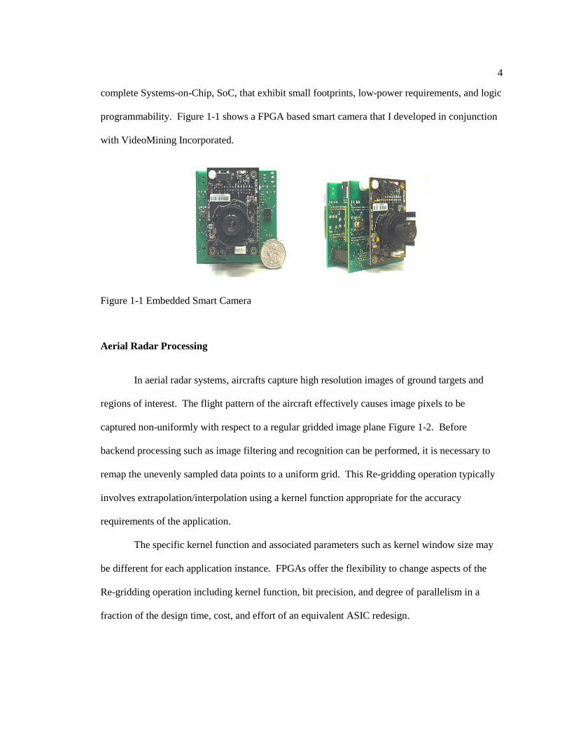
programmability. Figure 1-1 shows a FPGA based smart camera that I developed in conjunction
with VideoMining Incorporated.
Figure 1-1 Embedded Smart Camera
Aerial Radar Processing
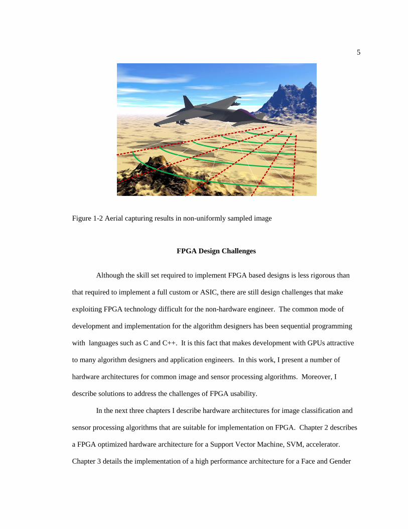
In aerial radar systems, aircrafts capture high resolution images of ground targets and
regions of interest. The flight pattern of the aircraft effectively causes image pixels to be
captured non-uniformly with respect to a regular gridded image plane Figure 1-2. Before
backend processing such as image filtering and recognition can be performed, it is necessary to
remap the unevenly sampled data points to a uniform grid. This Re-gridding operation typically
involves extrapolation/interpolation using a kernel function appropriate for the accuracy
requirements of the application.
The specific kernel function and associated parameters such as kernel window size may
be different for each application instance. FPGAs offer the flexibility to change aspects of the
Re-gridding operation including kernel function, bit precision, and degree of parallelism in a
fraction of the design time, cost, and effort of an equivalent ASIC redesign.
5
Figure 1-2 Aerial capturing results in non-uniformly sampled image
FPGA Design Challenges
Although the skill set required to implement FPGA based designs is less rigorous than
that required to implement a full custom or ASIC, there are still design challenges that make
exploiting FPGA technology difficult for the non-hardware engineer. The common mode of
development and implementation for the algorithm designers has been sequential programming
with languages such as C and C++. It is this fact that makes development with GPUs attractive
to many algorithm designers and application engineers. In this work, I present a number of
hardware architectures for common image and sensor processing algorithms. Moreover, I
describe solutions to address the challenges of FPGA usability.
In the next three chapters I describe hardware architectures for image classification and
sensor processing algorithms that are suitable for implementation on FPGA. Chapter 2 describes
a FPGA optimized hardware architecture for a Support Vector Machine, SVM, accelerator.
Chapter 3 details the implementation of a high performance architecture for a Face and Gender

6
Detecting neural network on FPGA. Chapter 4 illustrates an efficient Nearest Neighbor classifier
specifically designed for classifying gases that interact with chemiresistive nanowires. Chapter 5
introduces AlgoFLEX, an FPGA design framework for easing the task of integrating custom
accelerator cores into a high performance FPGA platform. Finally, Chapter 6 presents
conclusions and directions for future work.
Chapter 2
Support Vector Machine Accelerator
Many algorithms have been developed in the Machine Learning, Statistical Data Mining,
and Pattern Classification communities that perform image classification, detection, and
recognition tasks with remarkable accuracy. Many of these algorithms, however, when
implemented in software, suffer poor frame rates due to the amount and complexity of the
computation involved. This is particularly true for those applications which utilize Support
Vector Machines, SVM. This chapter presents an FPGA friendly implementation of a Gaussian
Radial Basis SVM well suited to human face classification tasks involving grayscale images.
Specifically, the implementation of a hardware efficient Support Vector Machine tailored for an
embedded gender classification system is described. A novel optimization of the SVM
formulation is identified that dramatically reduces the complexity of hardware implementations
of the algorithm. The benefits of this optimization are detailed in the implementation of a support
vector machine on modest sized FPGA. The implementation achieves 88.6% detection accuracy
which is to the same degree of accuracy of similar software implementations using the identical
classification mechanism.
Support Vector Machine Background
Support Vector Machines (SVM‟s) are becoming a common supervised-learning
technique used in pattern classification and recognition problems of high dimensionality and non-
linearity (Burges, 1998). Contrary to Artificial Neural Networks, ANN, in which a classification
task is defined by the weighted connections between neurons, SVM classification is defined
8
completely by a fixed set of operations on a set of so called Support Vectors. This fact lends
SVMs especially suitable in applications for which dynamically changing the particular
classification task is of high utility: the classification task can be easily modified by
reprogramming the Support Vectors. Moreover, SVMs prove to be as accurate –and in many
cases more accurate– than a corresponding ANN constructed from identical training data. The
primary limitation of SVM is the large number of non-trivial kernel function evaluations that
must be computed for each support vector. This work introduces a novel SVM architecture that
is feasible for FPGA implementation. The architecture is particularly efficient when input data is
represented with relatively small bit precision as it is in many image classification applications.
Support Vector
Support Vector
Support Vector
Margin
Margin/2
Class 1
Class 2
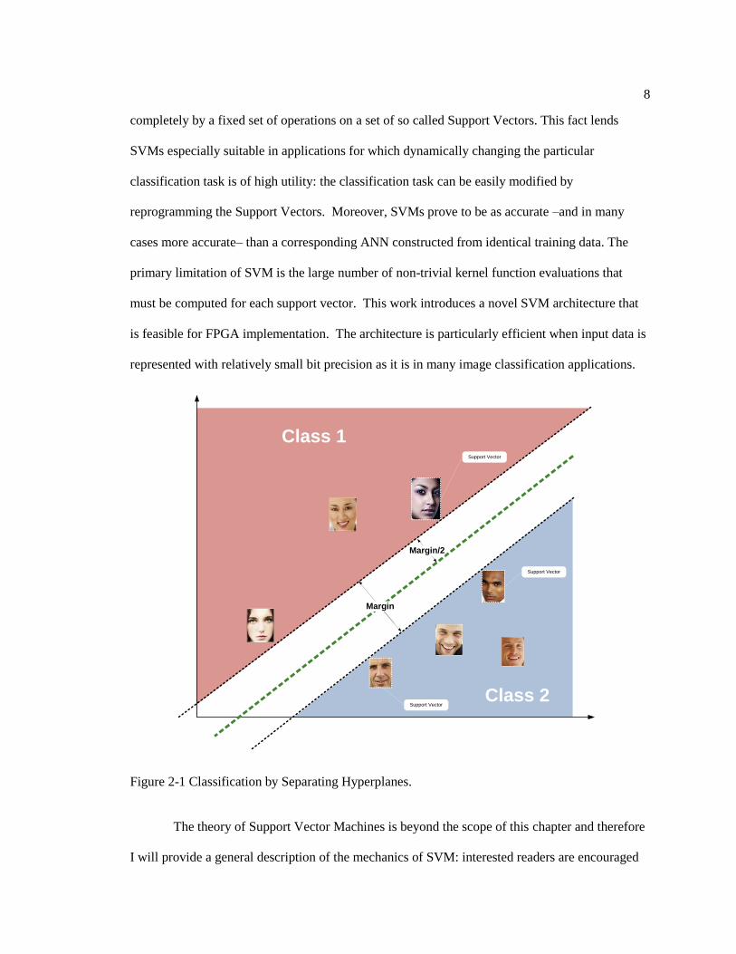
Figure 2-1 Classification by Separating Hyperplanes.
The theory of Support Vector Machines is beyond the scope of this chapter and therefore
I will provide a general description of the mechanics of SVM: interested readers are encouraged
9
to consult (Burges, 1998) for a rigorous introduction and tutorial on the subject. In a two class
problem, sample data may belong either to the positive class, 1, or the negative class, -1. During a
training phase, two parallel maximally separating hyperplanes are sought that separate points of
opposing class and have maximum distance between one another. The training points that lie on
these hyperplanes are of particular importance and are termed Support Vectors. During the
classification phase, the distance between an observed point and all support vectors are computed
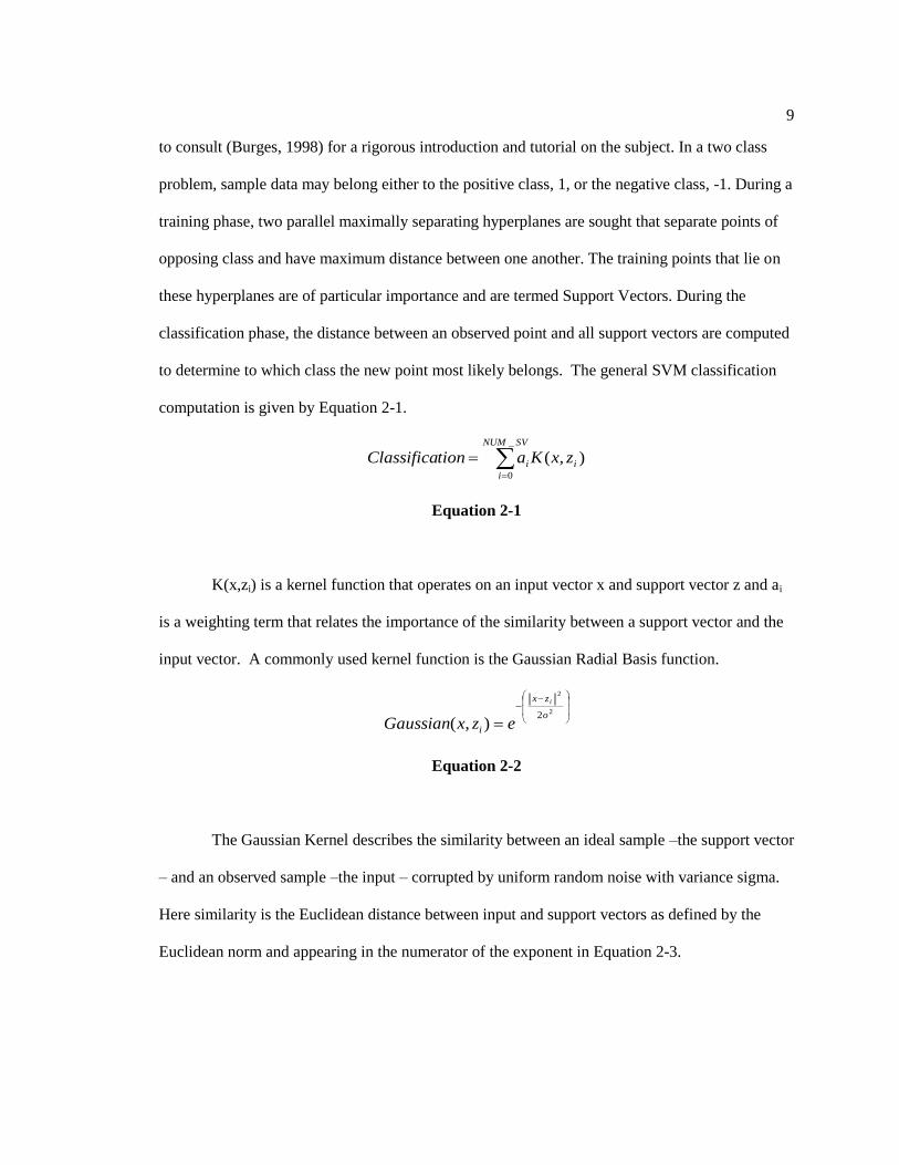
to determine to which class the new point most likely belongs. The general SVM classification
computation is given by Equation 2-1.
Equation 2-1
K(x,zi) is a kernel function that operates on an input vector x and support vector z and ai
is a weighting term that relates the importance of the similarity between a support vector and the
input vector. A commonly used kernel function is the Gaussian Radial Basis function.
Equation 2-2
The Gaussian Kernel describes the similarity between an ideal sample –the support vector
– and an observed sample –the input – corrupted by uniform random noise with variance sigma.
Here similarity is the Euclidean distance between input and support vectors as defined by the
Euclidean norm and appearing in the numerator of the exponent in Equation 2-3.
),(_
0
SVNUM
i
ii zxKationClassifica
2
2
2),(
o
zx
i
i
ezxGaussian

10
Equation 2-3
Input Representation
In the case of gender detection the SVM is applied to a fixed 30x30 image window
represented as a 900 element pixel vector. Each element in the vector is an 8-bit unsigned
grayscale pixel value with magnitude ranging from 0 to 255. Support vectors are defined
equivalently.
Kernel Optimization
The first step in optimizing the kernel function is to analyze the range of values that result
from the element-wise difference of the input image vector and a support vector when calculating
the Euclidean Norm. Since the elements in the input and support vectors are 8-bit values, there
difference is in the range of 255 to -255 and can be encoded as a 9-bit signed integer. Since
Equation 2-3 is interested in the squared differences, negative differences can be neglected and
the absolute differences can be encoded as 8-bit magnitudes.
Rewriting Equation 2-2 and substituting the Euclidean-Norm expansion allows the square
and square-root to cancel giving Equation 2-4.
Equation 2-4
211
2
00 ... nn zxzxzx
2
21,1
20,0
2
...
),(o
zxzx
i
nini
ezxGaussian

11
Before considering further manipulations of the kernel the following discussion will
highlight the implications of implementing the exponential function in hardware. Function
approximation can be accomplished using iterative methods or lookup tables. An iterative
technique most appropriate for hardware implementation is the CORDIC algorithm (Volder,
1959). CORDIC, like other iterative methods, exhibits low-performance and high device
utilization when implemented on FPGA. Lookup table approximation, when feasible, solves the
resource utilization shortcomings of iterative methods by packing function values into RAM
structures of current-day memory abundant FPGAs such as the Xilinx Virtex-4 family. In most
cases function approximation can be accomplished in a single cycle with single cycle read
latencies. The prohibitive limitation of the lookup table approach is that the table size grows
exponentially with the bit width of the indexing variable. For example, encoding exponents of
the Exponential function in 16-bits and encoding the Exponential function evaluation in 24-bits
results in a table size of roughly 1.5 Mb. This would consume 59% of BlockRAM resources of a
modest sized Xilinx Virtex-4 FX12 FPGA.
Referring to Equation 2-4, it is not immediately apparent how to utilize a lookup table.
Rewriting Equation 2-4 yields the following:
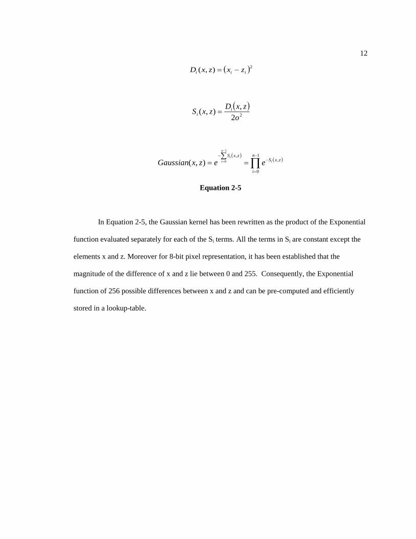
12
Equation 2-5
In Equation 2-5, the Gaussian kernel has been rewritten as the product of the Exponential
function evaluated separately for each of the Si terms. All the terms in Si are constant except the
elements x and z. Moreover for 8-bit pixel representation, it has been established that the
magnitude of the difference of x and z lie between 0 and 255. Consequently, the Exponential
function of 256 possible differences between x and z and can be pre-computed and efficiently
stored in a lookup-table.
2),( iii zxzxD
22
,),(
o
zxDzxS i
i
1
0
,,
1
0),(n
i
zxSzxS
i
n
i
i
eezxGaussian

13
DSP48DSP48-
MIN MAX
Support
Vector Fifo
Image
Vector Fifo
-
MIN MAX
-
MIN MAX
-
MIN MAX
-
MIN MAX
-
MIN MAX
-
MIN MAX
-
MIN MAX
Kernel
EXP(x)
DP BRAM
Kernel
EXP(x)
DP BRAM
Kernel
EXP(x)
DP BRAM
Kernel
EXP(x)
DP BRAM
MULT MULT MULT MULT
MULT MULT
MULT
MULT
Product Register
MULT
Outer Loop Weights
Weights
ADDER
Accumulator
=0
Classification
Figure 2-2 Initial architecture consisting of Exponential Function lookup tables followed by a
multiplier tree.

14
Initial Hardware Architecture
Figure 2-2 is a block diagram of a hardware embodiment of Equation 2-5 utilizing a
lookup-table for the Gaussian Kernel evaluation. Eight input vector and support vector elements
are accessed simultaneously from the input and support vector Fifos respectively. To ensure a
positive difference, a min/max unit routes the larger and smaller of the two unsigned operands to
the minuend and subtrahend ports of each subtractor respectively. Each Exponential Function
lookup-table is indexed by its associated subtractor output. The lookup-table output is delivered
into the Multiplier Tree which subsequently performs the series multiplication of the individual
Exponential terms. Following the last series multiplication, the product register holds the final
value of the current evaluation of the Gaussian Kernel. The kernel result is subsequently
multiplied by the appropriate weight (αi in Equation 2-1) and accumulated with previous
weighted kernel results. The process continues until the kernel has been evaluated for each
Support Vector.
The primary drawback of the architecture in Figure 2-2 is the multiplier tree. In addition
to consuming 21% of the DSP48 resources in the target Virtex-4 fx12 FPGA, the multiplier
would be responsible for the largest percentage of power consumption. More important, is the
loss of accuracy due to the frequent truncation necessary to keep intermediate products within the
range of the multipliers.
Fixed point notation is preferred over floating point notation because the precision gains
of floating point arithmetic are often outweighed by the latency and complexity of floating point
hardware realizations. For many applications the precision offered by a fixed point number
representation is sufficient and the hardware complexity of fixed point functional units is minimal
15
as the arithmetic operations are performed on integer functional units. One limitation of fixed-
point representation is its low dynamic range with respect to floating-point. This limitation is
most apparent when performing a series of fixed-point multiplications of n-bit and m-bit
numbers. The product of each multiplication is an n+m bit number with the number of fractional
bits equal to the sum of the fractional bits of the multiplier and the multiplicand. For example,
performing series multiplications of four 32-bit fixed-point numbers with 31 fractional bits would
result in a product with 124 fractional bits. This is infeasible for FPGA implementation. One
solution is to periodically truncate the product when the bit representation exceeds that of the
storage element or the multiplier input width. Since DSP48 resources on Virtex-4 FPGAs limit
multiplier operands to 18-bits, the multiplier outputs must be truncated appropriately before being
delivered into a proceeding stage of multiplication. It is this frequent truncation that leads to a
substantial loss of accuracy in the kernel evaluation.
Signed Log Computation
Performing the series multiplication in the logarithm domain can greatly reduce the
complexity of the architecture in Figure 2-2 and mitigate the loss of accuracy due to truncation.
In the Log Number System, LNS, the series multiplication of the Exp(-Si) terms translate to series
addition. Truncation is rarely, if ever, performed because the number of bits needed to encode the
accumulator grows at a substantially slower rate than in multiplication. However, the efficiency
gained from operating in the Log Number System can be outweighed by the cost in converting to
and from the logarithm domain: evaluating Logb x and AntiLog(x,b) respectively. The SVM
architecture outlined in the next section circumvents the need to evaluate Logb x online by taking
the logarithm of the kernel function when it is pre-computed offline and storing

16
Log(Kernel_Function) in the lookup table. In fact, it is not necessary to convert back to the
normal domain to make the final classification.
Adopting the LNS representation requires consideration of a minor subtlety:
intermediate SVM computations can involve negative numbers. Since logarithm is not defined
for negative numbers the architecture adopts the Signed Logarithm Number System, SLNS
(Swartzlander & Alexopoulos, 1975). SLNS represents a log number as a magnitude with an
appended sign bit. To ensure that Log(x) does not result in a negative number, SLNS represents
the log of a number x as Log(|kx|) where k is a positive scaling factor that guarantees Log(|kx|) is
greater than zero. Equation 2-6 gives the conversion. The definitions for the other arithmetic
operations of interest are given in Equations 2-7 through 2-9.
Equation 2-6
Equation 2-7
Equation 2-8
kAifL
kAifkAL
A
A
1,0
1),log(
)log(* kLLBA BA
ABB
BAA
LLifB
ALogLBALog
LLifA
BLogLBALog
,,1)(
,,1)(

17
Equation 2-9
As Equation 2-7 defines, multiplication becomes addition of the multiplier and
multiplicand minus the logarithm of the scale factor k. Note that addition and subtraction in
SLNS require an evaluation of Log(1+B/A) and Log(B/A–1) respectively. Since Log(B/A) =
Log(B) – Log(A), a lookup table can be employed to evaluate the original function with Log(B) –
Log(A) as the index. Referring to Equation 2-1 note that the evaluation of the SLNS addition is
only performed after the complete evaluation of the Gaussian Kernel for the input vector and a
given support vector. As such the addition only needs to be performed once every D cycles,
where D is the number of cycles needed to complete the differences between the input vector and
the support vector. As a consequence, in most cases, the function evaluation is not in the critical
path of the SVM computation and more sophisticated –and time consuming- techniques for
approximating Log(1+B/A) and Log(B/A–1) can be employed if accuracy requirements justify
its necessity.
ABB
BAA
LLifB
ALogLBALog
LLifA
BLogLBALog
,,1)(
,,1)(

18
DSP48DSP48-
MIN MAX
Support
Vector Fifo
Image
Vector Fifo
-
MIN MAX
-
MIN MAX
-
MIN MAX
-
MIN MAX
-
MIN MAX
-
MIN MAX
-
MIN MAX
Correction Value
Log(NumSV*k)
Outer Loop Weights
SgnLNS(weights) Kernel
Log(EXP(x))
DP BRAM
Kernel
Log(EXP(x))
DP BRAM
Kernel
Log(EXP(x))
DP BRAM
Kernel
Log(EXP(x))
DP BRAM
ADDER ADDER
DSP48 Tile
ADDER ADDER
DSP48 Tile
ADDER ADDER
DSP48 Tile
ADDER ADDER
DSP48 Tile
-
MIN MAX
Truncation
Log-Add
Lookup
SP BRAM
Log-Sub
Lookup
SP BRAM
ADDER
Sign
=
Sign(Weights[i])
1 0
Magnitude Accumulator
Classification
Figure 2-3 Improved SVM architecture replacing multiplier tree with adder tree and utilizing
LogAdd/LogSub lookup tables.
Efficient Hardware Architecture
Figure 2-3 is a block diagram of the hardware embodiment of Equation 2-5 utilizing
lookup-tables for the Gaussian Kernel evaluation and SLNS for backend computation. The
improved architecture is equivalent to that in Figure 2-2 up to the output of the lookup tables

19
which in this version is in SLNS fixed-point representation. Each lookup-table output is presented
into an input of a dedicated adder that computes the sum of the lookup-table output and the partial
sum of a neighboring adder in a cascaded adder chain. Effectively there are eight partial sums that
propagate through the adder chain that must ultimately be accumulated before the Gaussian
evaluation is complete. The primary adder, denoted with a P in Figure 2-3, is responsible for the
final accumulation of the partial sums, addition of Log(k*weighti), and subtraction of
Log(scale_factor) for the total number of additions.
Once the kernel evaluation completes, the current positive weighted result has to be
added to the accumulation of previous weighted kernel evaluations (the summation in Equation 2-
1). Because the new result is signed -as determined solely by the sign of the weight associated
with the current iteration- and the current accumulation is signed -as determined by its sign bit -
it will be necessary to perform either sign-magnitude addition or subtraction in the SNLS domain.
As Equations 2-8 and 2-9 show, log addition and subtraction requires evaluation of a function of
the ratio of the two operands in normal domain or their difference in logarithm domain. By
guaranteeing that Log(B) >= Log(A) it is ensured that their difference is positive. Therefore the
size of each lookup-table is reduced by half of that necessary for arbitrary magnitude
relationships between the operands (Melnikoff & Quigley, 2003). This convenience comes at the
expense of an additional max/min selection unit. The choice of which table to index is
determined by the similarity of the signs of the two operands: like signs invoke addition and
subtraction otherwise. The tables are indexed by the truncated difference of the two operands.
Finally, the lookup table output is summed with the minimum of the two operands while the sign
of the result is computed as the sign of the largest magnitude operand.
20
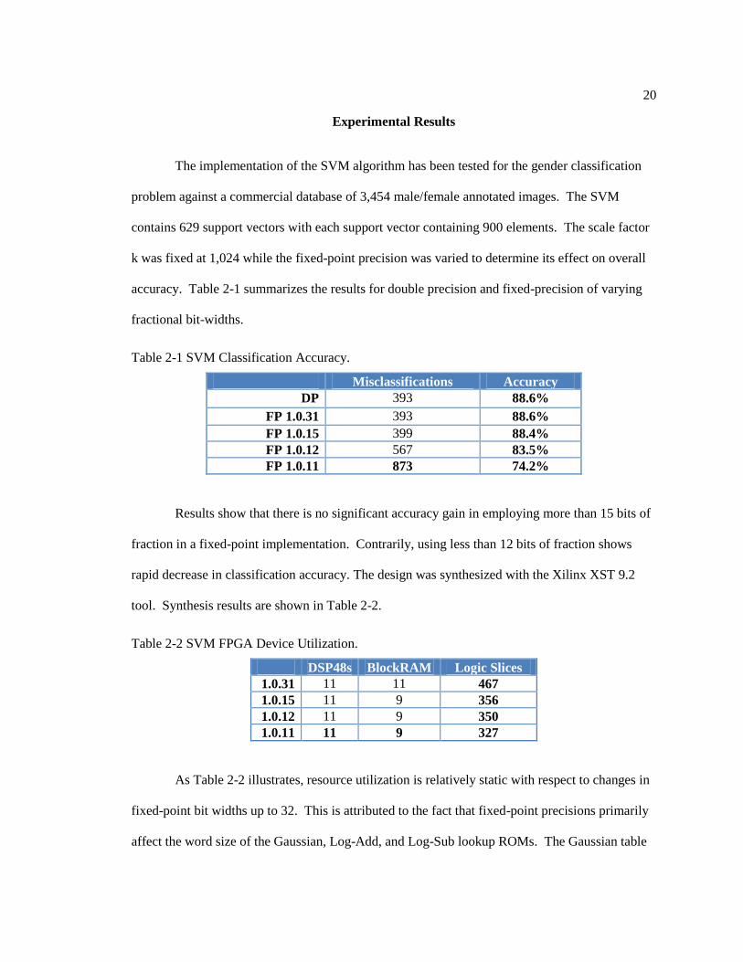
Experimental Results
The implementation of the SVM algorithm has been tested for the gender classification
problem against a commercial database of 3,454 male/female annotated images. The SVM
contains 629 support vectors with each support vector containing 900 elements. The scale factor
k was fixed at 1,024 while the fixed-point precision was varied to determine its effect on overall
accuracy. Table 2-1 summarizes the results for double precision and fixed-precision of varying
fractional bit-widths.
Table 2-1 SVM Classification Accuracy.
Misclassifications Accuracy
DP 393 88.6%
FP 1.0.31 393 88.6%
FP 1.0.15 399 88.4%
FP 1.0.12 567 83.5%
FP 1.0.11 873 74.2%
Results show that there is no significant accuracy gain in employing more than 15 bits of
fraction in a fixed-point implementation. Contrarily, using less than 12 bits of fraction shows
rapid decrease in classification accuracy. The design was synthesized with the Xilinx XST 9.2
tool. Synthesis results are shown in Table 2-2.
Table 2-2 SVM FPGA Device Utilization.
DSP48s BlockRAM Logic Slices
1.0.31 11 11 467
1.0.15 11 9 356
1.0.12 11 9 350
1.0.11 11 9 327
As Table 2-2 illustrates, resource utilization is relatively static with respect to changes in
fixed-point bit widths up to 32. This is attributed to the fact that fixed-point precisions primarily
affect the word size of the Gaussian, Log-Add, and Log-Sub lookup ROMs. The Gaussian table

21
depth is fixed at 256 entries and the depth of the Log-Add and Log-Sub tables were fixed at 2048
in our experiments. Control logic remains constant across various bit-widths with minor changes
mostly caused by variations in data path width.
The SVM architecture can gender classify a single 30x30 image window with 629
support vectors in 843 microseconds when running at 100 MHz operating frequency. The
implementation can process 38 such image windows in a 33 millisecond frame period and
maintain real-time frame rates of 30 fps.
Conclusion
The Support Vector Machine architecture was implemented in the Verilog HDL and
synthesized using the Xilinx ISE 9.2™ design tools. Simulation was performed using Mentor
Graphics ModelSim® simulation suite. Software simulation, used for accuracy comparison
purposes, was implemented in the C# programming language. The gender classification hardware
implementation, achieves 88.6% detection accuracy which is extremely competitive with existing
software implementations.

Chapter 3
Streaming Artificial Neural Network
In this chapter, I, describe an FPGA implementation of a streaming artificial neural
network architecture that has been configured to perform face detection and gender classification
on real-time video streams. The system was implemented on a Virtex-4 FX12 FPGA from Xilinx.
The results show 94.6% and 83.0% accuracy for real-time face detection and gender recognition,
respectively.
Artificial Neural Networks, or ANNs, are biologically inspired connection-oriented
computation models capable of discerning non-linear relationships from noisy data. This work
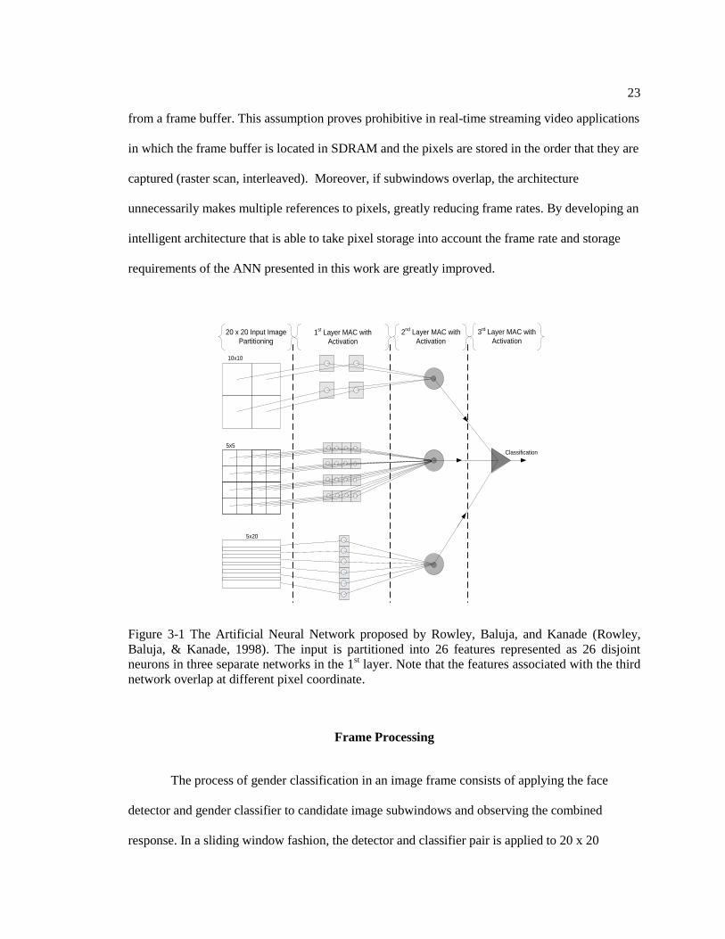
employs the ANN illustrated in Figure 3-1, first proposed by Rowley, Baluja, and Kanade
(Rowley, Baluja, & Kanade, 1998), where an image is first partitioned into three sub-images.
This partitioning divides the image into 4, 16, and 6 input neurons to isolate different features
within the image known to correspond to human faces.
An architecture that performs face detection in hardware has been presented in (Irick,
Theocharides, N., & Irwin, 2006). The work presented was done on a single Virtex-II Pro (V2Pro
30, speedgrade 7) FPGA where both benefits and tradeoffs of implementing an ANN in hardware
were discussed. In the work presented an ANN hardware implementation was proposed that was
based on (Rowley, Baluja, & Kanade, 1998). The system operated on a 20 x 20 image patch and
utilized a fixed point number representation to circumvent complicated floating point hardware.
Interestingly, by exploiting properties of the ANN‟s computation this architecture was able to
achieve 94% detection accuracy for a 20 x 20 image and was able to run at 40 fps for a 320 x 240
image over 8 scales. However, the architecture suffered from several limitations. First, it was
limited to applications in which the pixels that constitute a subwindow are randomly accessible
23
from a frame buffer. This assumption proves prohibitive in real-time streaming video applications
in which the frame buffer is located in SDRAM and the pixels are stored in the order that they are
captured (raster scan, interleaved). Moreover, if subwindows overlap, the architecture
unnecessarily makes multiple references to pixels, greatly reducing frame rates. By developing an
intelligent architecture that is able to take pixel storage into account the frame rate and storage
requirements of the ANN presented in this work are greatly improved.
10x10
Classification
20 x 20 Input Image
Partitioning1
st Layer MAC with
Activation
2nd
Layer MAC with
Activation
3rd
Layer MAC with
Activation
5x5
5x20
Figure 3-1 The Artificial Neural Network proposed by Rowley, Baluja, and Kanade (Rowley,
Baluja, & Kanade, 1998). The input is partitioned into 26 features represented as 26 disjoint
neurons in three separate networks in the 1st layer. Note that the features associated with the third
network overlap at different pixel coordinate.
Frame Processing
The process of gender classification in an image frame consists of applying the face
detector and gender classifier to candidate image subwindows and observing the combined
response. In a sliding window fashion, the detector and classifier pair is applied to 20 x 20

24
subwindows at each row and column offset defined by vert_step and horz_step, respectively
(Figure 3-2). The number of subwindows processed is a function of the image dimensions and
the degree of horizontal and vertical overlap defined respectively by the horizontal and vertical
step size (Equations 3-1, 3-2, and 3-3).
Equation 3-10
Equation 3-2
Equation 3-3
Thus, for a 320 x 240 image, with single pixel offsets in both vertical and horizontal directions,
there is a maximum of 66,521 subwindows that may be generated.
There is also the issue of processing faces that are at varying distances from the capture
device while using a fixed window size. A classification system that does not incorporate a size
invariance mechanism will not properly detect and classify faces that are too large to fit within a
20 x 20 window. A standard scheme for making a recognition task size invariant is to normalize
the image at multiple scales of decreasing image resolution (Wiskott, 2004). By successively
decreasing the image size, large faces will eventually be fully contained within a single 20 x 20
subwindow. Furthermore, since the image size reduces as the image is sub-sampled the number
image_width 20_ 1
h_offsetnum hsubwindows
image_height 20_ 1
v_offsetnum vsubwindows
_ _ * _num subwindows num hsubwindows num vsubwindows

25
of subwindows generated for a particular scale will also decrease, subsequently reducing the
amount of computation needed. However, to formulate a representative upper bound on
performance the worst-case scenario is assumed: each scale requires the evaluation of the
maximum number of subwindows corresponding to the largest image resolution and the
maximum degree of overlap. Sequential processing of each subwindow results in low frame rates
due to poor data reuse and irregular memory access patterns.
Figure 3-2 Subwindow overlapping due to offsetting. The numbers indicate the number of
overlapping subwindows at that intersection. As the image is scaled the number of subwindows
necessary to cover the entire image reduces.
Data Reuse
Pixel_use is defined as the number of times a given pixel, pij, is used in classifying an
image with horizontal and vertical offsets h_offset and v_offset. This quantity is equivalent to the
number of subwindows that contain pixel pij. Further, Max_Pixel_Use is defined as the maximum
number of occurrences of a pixel for all subwindows in the image. Max_Pixel_Use is equal to the
maximum number of overlapping subwindows and is defined as:

26
20 20_ _
_ _Max Pixel Use
h offset v offset
Equation 3-4
In an ideal implementation, the number of parallel resources, m, necessary to compute all
current and future values dependent on the current pixel is proportional to Max_Pixel_Use. The
primary limitation of the sequential architecture, in which m = 1, is that it does not consider future
computations involving the current pixel. A streaming approach with scalable resources will be
able to match m closely to Max_Pixel_Use making it suitable to meet application requirements.
Memory Access
High performance memory-to-peripheral interfaces are critical for sustaining high data
rates to an accelerator. Memory-to-peripheral transaction times are dominated by three factors:
bus arbitration time, read setup time, and transfer time. In high performance peripheral
interconnects, memory-to-peripheral transactions are optimized for data bursting of sequential
address locations so as to amortize arbitration and setup times with efficient data transfers. If
addresses are known to be sequential the memory controller‟s state machine can provide data on
every cycle following the read setup time.
Consider the 64-bit IBM CoreConnect bus provided by Xilinx for use within their
FPGAs. The specification allows for a maximum of sixteen 8-byte burst transfers. The sequential
ANN, described in Section 2, is only able to process twenty pixels (1-byte) in a row before
proceeding to the next row. Assume 20 x 20 subwindows are extracted directly from the full
image (i.e. 320 x 240); intra-row pixels are stored sequentially; and inter-row pixels are stored at
a distance equal to the stride of the image. The percentage of the theoretical peak bursting

27
bandwidth that the sequential ANN uses is then defined by the ratio of bursts that should take
place and those that must actually take place. More formally, Equations 3-5 and 3-6 describe the
utilization.
_#_ _ Stride
Max Burstof Bursts
Equation 3-5
#_ _
#_ _* 100
of Bursts
of Burstsutilization
Equation 3-6
As an example, consider the 20 x 20 pixel case :
20#_ _ ( ) .15625
128
.15625 100% 15.6%
1
of Bursts sequential
Utilization
This comes from the fact that bursts have to be multiples of the bus width (specified in bytes) and
it is not possible to have a burst that is a fraction of the maximum burst length. As I will show in
the next section, by minimizing successive accesses to a single pixel and constraining pixel
accesses to the order in which they are stored, dramatic performance improvements are achieved.
By operating on the data in a streaming fashion, bus utilization is increased.
320#_ _ 2.5
128
2.5 100% 83.3%
3
of Bursts
Utilization

28
Hardware Architecture
Figure 3-3 illustrates the streaming architecture that was implemented. Pixels of the
image frame are presented to the system in the order in which they are stored. For most non-
compressed real-time video applications this order is typically raster scan. In this architecture,
multiple subwindows are “live”, or in progress, for a given pixel in the input stream. In effect the
architecture gains higher performance by optimizing dataflow at the expense of control state
complexity and intermediate data storage requirements.
In a single pixel cycle the Pixel Processing Unit processes all of the active neurons in the
1st layer, where an active neuron is one whose bounding box includes the current pixel pij. Since
there are three disjoint networks in layer 1, there are a minimum of three active neurons for a
given pixel. However, due to the overlapped structure of the six neurons in network three, some
pixels will activate 4 neurons. For simplicity of discussion, network 3 is divided into 2 neuron
sets. The first set, Set 1, includes neurons 1, 3, and 5 while the second set, Set 2, includes
neurons 2, 4, and 6. As pixels stream into the Pixel Processing Units, neuron accumulations
subsequently complete and their final values are forwarded to one of three neurons in the 2nd
layer. Similarly, the layer 2 neurons forward their final results to a single neuron in the output
layer. The neuron completion times for a particular subwindow are interleaved with those of
other subwindows assigned to the Pixel Processing Unit.

29
Port A
(Write)
Port B
(Read)
Control
Context
raddr
DSP48
BlockRAM
waddr
+
DSP48
Th
resh
old
s
+
{pixel,
row,
column,
valid}
X
X
Port A
(Read)
BlockRAM
Accumulator
Tanh Table
Face
GenderABS(x)
Control
Out
SM
to
TwosTanh(Gender) to PPU[1..4]
Tanh(Face Detection) to PPU[1..4]
Destination Control to PPU[1..4]
PPU[1]
PPU[2]
PPU[3]
PPU[4]
FD
Weight
ROM
GC
Weight
ROM
ARB
Threshold Index Weight IndexAccum Addr Accum Done?
Output Format
Pixel Cycle
PPU Cycle
{pixel, row, column, valid}
add(1)mult(1)
fetch(1)
out format
update(1)
add(2)mult(2)
fetch(2)
out format
update(2)
add(3)mult(3)
fetch(3)
out format
update(3)
add(4)mult(4)
fetch(4)
out format
update(4)
FD Data GC Data Context
Subwindow Target NeuronPPU #
C)
A)
B)
Result QueueResult QueueSystem
Output
Pixel[1]
(Decode)
Pixel[2]
(Decode)
t = 0 t = 1 t = 2 t = 3 t = 4 t = 5 t = 6
FB Queue
1
2
1
3
3
1
0
0
02
1
2
Phase 1
Phase 2
Phase 3
Phase 4
Port B
(Read)
Figure 3-3 (A) PPU and SAU block diagram. Dual-Pipe PPUs are instantiated as necessary for a
given image size. (B) Control and data format (C) Pipeline chart. The PPU pipeline consists of 4
stages: decode, fetch/multiply, add, and update/output format.
30
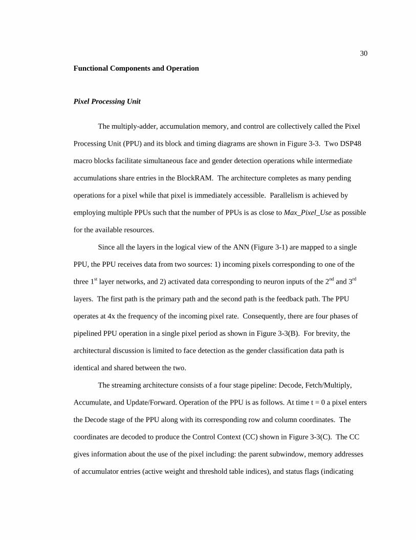
Functional Components and Operation
Pixel Processing Unit
The multiply-adder, accumulation memory, and control are collectively called the Pixel
Processing Unit (PPU) and its block and timing diagrams are shown in Figure 3-3. Two DSP48
macro blocks facilitate simultaneous face and gender detection operations while intermediate
accumulations share entries in the BlockRAM. The architecture completes as many pending
operations for a pixel while that pixel is immediately accessible. Parallelism is achieved by
employing multiple PPUs such that the number of PPUs is as close to Max_Pixel_Use as possible
for the available resources.
Since all the layers in the logical view of the ANN (Figure 3-1) are mapped to a single
PPU, the PPU receives data from two sources: 1) incoming pixels corresponding to one of the
three 1st layer networks, and 2) activated data corresponding to neuron inputs of the 2
nd and 3
rd
layers. The first path is the primary path and the second path is the feedback path. The PPU
operates at 4x the frequency of the incoming pixel rate. Consequently, there are four phases of
pipelined PPU operation in a single pixel period as shown in Figure 3-3(B). For brevity, the
architectural discussion is limited to face detection as the gender classification data path is
identical and shared between the two.
The streaming architecture consists of a four stage pipeline: Decode, Fetch/Multiply,
Accumulate, and Update/Forward. Operation of the PPU is as follows. At time t = 0 a pixel enters
the Decode stage of the PPU along with its corresponding row and column coordinates. The
coordinates are decoded to produce the Control Context (CC) shown in Figure 3-3(C). The CC
gives information about the use of the pixel including: the parent subwindow, memory addresses
of accumulator entries (active weight and threshold table indices), and status flags (indicating

31
accumulation completion following processing of the current pixel). The pixel and context are
registered in global registers at the rising edge of the clock and remain constant for four PPU
clock cycles.
The Fetch/Multiply stage begins at time t = 1. At this time the pixel and the current
weight are presented to the input of the DSP48 multiplier and the accumulator address is
presented to the read address port of the BlockRAM. The Fetch operation consists of reading the
accumulator memory for the referenced entry, while the multiplier computes the product of the
pixel and the weight. The outputs generated from the memory and multiplier are registered into
pipeline registers at the rising edge of the PPU clock edge. Finally, the accumulator read address
is registered into the first entry of a two entry Address Delay Pipe.
The Accumulate stage begins at time t = 2. The weighted-pixel is presented to the
primary input of the DSP48 adder and the retrieved accumulator value is presented to the
secondary input of the adder. At the end of the Accumulate stage the adder output register
contains the sum of the weighted-pixel and the current accumulator value. The delayed read
address progresses to the last entry in the Address Delay Pipe.
The Update/Forward stage begins at time t = 3. The registered adder output is presented
to the input of the write data port of the memory while the delayed read address is presented to
the write address port of the memory and the read address port of the threshold array. If the
current pixel is not the last pixel in the neuron, memory is updated with the new accumulator
value. Contrarily, if the pixel is the last pixel in the neuron, a sign-magnitude representation of
the accumulator result is forwarded to the output queue and the memory is initialized with the
biasing constant. In addition, control information is generated to accompany the data through the
Shared Activation Unit.
One pixel cycle consists of four phases of time shared MAC operations. Phase 1 and 2
are associated with processing pixels in networks 1 and 2, respectively. Neurons 1, 3, and 5, of

32
network 3, are processed in Phase 3; while neurons 2, 4, and 6, of network 3, are processed in
Phase 4. Dead phases are PPU cycles in which there is a valid pixel available, however there is
no processing to be performed for the current phase. Dead phases can only occur in phases 3 and
4 where only six of the neurons are active. Instead of allowing the PPU to remain idle during
these times, the PPU is reused to process data from the feedback queue (activated values from
layers 2 and 3). The size of the feedback queue is bounded because the generation of layer 2‟s
and layer 3‟s data occur as a result of input stream progression. Feedback data proceeds through
the four pipeline stages in the same fashion as primary data.
Shared Activation Unit
Once all the pixels in a neuron have been weighted and accumulated the final
accumulated value is activated by a nonlinear function: hyperbolic tangent (tanh). It is worth
mentioning that although there are many numerical methods for approximating nonlinear
functions, lookup tables achieve the highest performance where relatively low-precision is
required. The tanh function is mapped to a dual-ported BlockRAM where each port is shared by
four PPUs. The activation table and support logic are collectively named the Shared Activation
Unit (SAU).
Accumulated values enter the SAU in sign-magnitude representation along with control
information for routing the activated result back to the originating PPU. An input multiplexer and
arbiter combination selects from multiple requesting PPUs. Data-Control packets traverse the
SAU in two separate pipelines, the data and control pipes. The data pipeline consists of the
BlockRAM based activation table and a sign-magnitude to two‟s-complement converter. The
control pipeline consists of delay stages necessary to keep data and control synchronized and an
output selector for determining the proper output queue of the result.

33
The penalty for highly virtualizing the functional units is an increase in storage
requirements for both data and control state. To minimize the storage requirements the following
scheme is used: First, a slice is defined as the set of non-overlapping subwindows beginning at
horizontal offset 0 and vertical offset v, and ending at horizontal offset w and vertical offset v +
20, where w is the image width. Next, slices are assigned to PPUs such that a PPU does not
operate on overlapping slices. All resources allocated for subwindows in a slice are released when
the input stream proceeds beyond the slice boundaries. Since storage can be reused across
disjoint slices, storage complexity reduces from Θ(m2) to Θ(m).
Figure 3-4 Frame Rate vs. Overlap vs. #PPU(s)
0
50
100
150
200
250
1 2 4 8
Fra
me
Ra
te
# of PPUs
16-pixel Overlap 15-pixel Overlap
13-pixel Overlap 10-pixel Overlap

34
Figure 3-5 Frame Rate vs. Number of Scales
Table 3-1 NN FPGA Device Utilization
Resource PPU SAU Total (4 PPUs) Total Device %
Slices 552 399 1,407 26 %
Registers 228 519 1,431 13 %
LUT 435 638 2,378 22 %
DSP48 4 0 16 50 %
BRAMs 2 2 10 28 %
Table 3-2 NN Classification Accuracy
Face No-Face Female Male
Totals 13,195 21,805 2,050 1,812
Classified 12,197 20,905 1,795 1,423
Mis-Classified 998 900 255 389
Accuracy 94.6 % 83.3%
Worst and Typical Frame Rate vs. Number of Scales
51.6
4
47.6
2
43.2
9
39.6
8
174.8
2
172.5
3
170.7
4
169.2
7
169.2
7
169.2
7
169.2
7
169.2
7
169.2
7
31.7
5
29.7
6
28.0
1
34.0
1
36.6
3
0
50
100
150
200
250
18 20 22 24 26 28 30 32 34
Number of Scales
Fra
me R
ate
Worst (100% Scale) Typical (90% Scale)
35
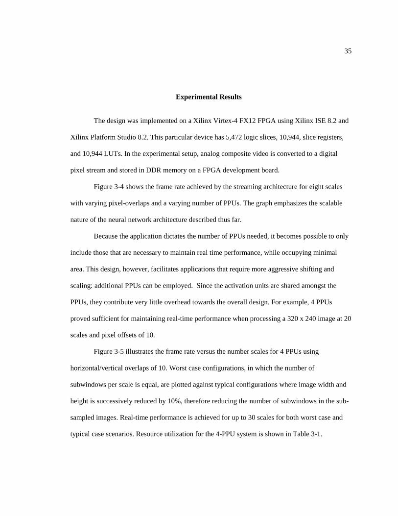
Experimental Results
The design was implemented on a Xilinx Virtex-4 FX12 FPGA using Xilinx ISE 8.2 and
Xilinx Platform Studio 8.2. This particular device has 5,472 logic slices, 10,944, slice registers,
and 10,944 LUTs. In the experimental setup, analog composite video is converted to a digital
pixel stream and stored in DDR memory on a FPGA development board.
Figure 3-4 shows the frame rate achieved by the streaming architecture for eight scales
with varying pixel-overlaps and a varying number of PPUs. The graph emphasizes the scalable
nature of the neural network architecture described thus far.
Because the application dictates the number of PPUs needed, it becomes possible to only
include those that are necessary to maintain real time performance, while occupying minimal
area. This design, however, facilitates applications that require more aggressive shifting and
scaling: additional PPUs can be employed. Since the activation units are shared amongst the
PPUs, they contribute very little overhead towards the overall design. For example, 4 PPUs
proved sufficient for maintaining real-time performance when processing a 320 x 240 image at 20
scales and pixel offsets of 10.
Figure 3-5 illustrates the frame rate versus the number scales for 4 PPUs using
horizontal/vertical overlaps of 10. Worst case configurations, in which the number of
subwindows per scale is equal, are plotted against typical configurations where image width and
height is successively reduced by 10%, therefore reducing the number of subwindows in the sub-
sampled images. Real-time performance is achieved for up to 30 scales for both worst case and
typical case scenarios. Resource utilization for the 4-PPU system is shown in Table 3-1.

36
The architecture makes judicious use of the embedded DSP48 and BlockRAM resources
of the Xilinx Virtex-4 FPGA in order to minimize the use of logic resources. Accuracy results
are shown in Table 3-2. The face detector was trained using 20,000 images and was tested on a
separate database of 35,000 images, achieving 94.6% accuracy. The remaining inaccuracies
where due to 2.9% of the images being classified as false positives (detected face when no face
existed) and 2.6% being classified as false negatives (detected no face when face existed). The
gender detector was trained with 200,000 images and was tested on a separate database of 3,862
images, achieving 83% accuracy overall.
Conclusion
This chapter presented the implementation of a novel architecture for performing face
detection and gender recognition using a popular Artificial Neural Network architecture. The
intelligently designed FPGA architecture maximizes the utilization of the computation pipeline
by taking advantage of the spatial locality of pixels that exists within memory and the neural
network structure. The design was implemented and tested on a Xilinx Virtex-4 FPGA where
each PPU only required 252 slices. The entire system required a total of 1,407 logic slices
including 4-PPUs, one activation unit and a moderate amount of glue logic. With an FPGA
geared towards embedded systems, such as the FX12, this implementation utilized less than 30%
of the total chip resources leaving ample room for other components. Further, the implementation
achieved real-time performance while detecting and classifying human faces with accuracy
comparable to leading commercial software.

Chapter 4
Nearest Neighbor Classifier for Gas Sensing Applications
This chapter explores the design issues in the implementation of a pattern classifier for a
gas sensor system. The objective of this research is to design sensor platforms based on an array
of chemi-resistive sensors integrated with a configurable pattern classifier for identifying gas
mixtures. Since there are no current FPGA systems that currently integrate with sensor systems,
the scope of implementation is limited to a simulation-based study.
Nanoscale Sensor Arrays
The integration of hundreds of nanoscale sensors on a single chip to mimic olfactory
systems of mammals has several application domains including homeland security and the food
and drug industry. Electronic “noses” employing macro scale sensors have been successfully
used in a variety of applications such as determining breath alcohol levels (Mitsubayashi,
Matsunaga, Nishio, Ogawa, & Saito, 2004), inspecting automotive exhaust emissions for safety
(Valleron, Pijolat, Viricelle, Breuil, Marchand, & Ott, 2009), and determining food quality
(Sinesio, et al., 2000). The primary disadvantage of macro scale sensors, however, is their
inability to detect miniscule traces of a variety of gases in a power and area-efficient manner.
Nanosensor arrays are especially suited to address these drawbacks and are ideal for building
low-power single-chip “nano-noses” This chapter focuses on the design of a nanosensor array-
based gas discrimination system.
There are several issues that need to be addressed in designing a complete nanosensor
based gas classifier: namely, nanosensor fabrication, accurate alignment of the nanosensors with

38
interface circuitry, design of appropriate interface and conversion circuitry, and design of a robust
pattern classifier to properly interpret sensor response. This work focuses on the design of the
pattern classifier system and provides brief overview of the other system components. Most
closely related to this work is that by (Xu, N., Xie, & Irwin, 2004) which proposed a gas
detection system based on chemiresistive nanosensors. Contrary to simply detecting the presence
or absence of a particular gas, the system implemented in this study is capable of classifying a
variety of compound mixtures of gases. This work utilizes a distributed pattern classifier, in
contrast to the off-chip software based solution presented in (Xu, N., Xie, & Irwin, 2004). The
organization of the chapter is as follows. A background of nanowire sensors is presented in
Section 2. The procedure for integrating the nanowires with the pattern classifier circuitry is
explained in section 3. Section 4 provides an overview of the interface electronics between the
sensors and the pattern classifier. Sections 5 and 6 provide details of the system operation and
pattern classifier architecture. Section 7 is the conclusion.
Cross-Reactive nanosensors are practical in applications in which the primary objective is
to recognize the presence or fidelity of compound mixtures of gases. The measure of response of
a nanowire to gaseous substances is a deviation of resistance (or conductance) across the chain of
polymer grains with respect to the ambient resistance (Williams & Pratt, 1996).
Sensor and Processor Integration
Nanosensors are positioned above the processing circuitry on the external layer of the
CMOS die using a Post-IC placement technique based on electro fluidic alignment (Smith,
Nordquist, Jackson, Mayer, Martin, & Mbindyo, 2000). In this process, an electric field is applied
to buried electrodes implemented in metal 4 layer (see Figure 4-1), which couples capacitively
with the contacting electrodes implemented in metal 5 layer. The nanowires are aligned to the

39
contacting electrodes by the induced electric field and are secured via deposition of metal at the
junction of the electrodes and the sensor tips using a standard metal liftoff process. Sensor
placement is considered successful if after final alignment a nanowire provides a resistive bridge
–no short or open circuit– across matting electrodes. Yields of 60% have been reported in recent
tests conducted by our collaborators.
Figure 4-1 Nanosensor physical interface and geometries. Nanosensors (yellow and black wires)
are bridged across contacting electrodes (green), and secured with metal deposits (silver ovals) at
the junctions.
Interface Electronics
The interface electronics subsystem measures the deviation in resistances of the
nanosensors and conditions and converts the small analog signals to digital quantities for input
into the pattern classifier. Among the most common circuits used to measure resistive sensors are
the Wheatstone Bridge (Miner & Comer, 1992), Voltage Divider (Miner & Comer, 1992), and
Anderson Loop (Anderson, 1998). The output of the measurement circuitry is translated into a
digital value by a low resolution ADC that divides the sensor response into three regions
summarizes as follows: in the absence of a reacting compound, the output of the ADC is “00”. If
the resistance of the nanowire increases above Rthreshold1, but not exceeding Rthreshold2 the
output of the ADC is “01”. Similarly, if the resistance of the nanowire increases above

40
Rthreshold2, the output is “10”. Since several target gases fall into the same category using a
single chemiresistive sensor, it is beneficial to further classify the gases using two or more sensor
types. In particular, this design combines the responses from three sensor types to distinguish
target gases into twenty seven distinct categories. Note that in this design it is possible to share
the interface electronics with multiple sensors that can be polled sequentially. This time
multiplexing feature is afforded by the relatively slow response times of the sensors to gases.
PE PE PE PE
PE PE PE
PE PE PE PE
PE PE PE PE
IE
(ADC)
Router
Virtual Label
Registers
Control
Accumulator
PE
Figure 4-2 Processing Element, PE, array architecture and internals of a single PE.
Classifier Architecture
An effective cross-reactive sensing system requires a robust pattern classifier that reliably
and reproducibly detects gas compounds of interest while operating in environments that differ
considerably from the initial training environment. This section details the theory of operation of
a 3D pattern classifier based on the 2D cell automaton architecture proposed in (P. G. Tzionas,
1994). Figure 4-2 illustrates the pattern classifier architecture consisting of an array of m x n PEs.
Each PE consists of the interface electronics unit, an accumulator, routing unit, control unit and a
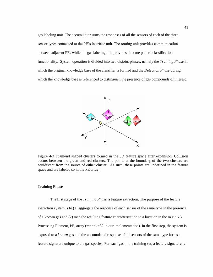
41
gas labeling unit. The accumulator sums the responses of all the sensors of each of the three
sensor types connected to the PE‟s interface unit. The routing unit provides communication
between adjacent PEs while the gas labeling unit provides the core pattern classification
functionality. System operation is divided into two disjoint phases, namely the Training Phase in
which the original knowledge base of the classifier is formed and the Detection Phase during
which the knowledge base is referenced to distinguish the presence of gas compounds of interest.
Figure 4-3 Diamond shaped clusters formed in the 3D feature space after expansion. Collision
occurs between the green and red clusters. The points at the boundary of the two clusters are
equidistant from the source of either cluster. As such, these points are undefined in the feature
space and are labeled so in the PE array.
Training Phase
The first stage of the Training Phase is feature extraction. The purpose of the feature
extraction system is to (1) aggregate the response of each sensor of the same type in the presence
of a known gas and (2) map the resulting feature characterization to a location in the m x n x k
Processing Element, PE, array (m=n=k=32 in our implementation). In the first step, the system is
exposed to a known gas and the accumulated response of all sensors of the same type forms a
feature signature unique to the gas species. For each gas in the training set, a feature signature is

42
obtained from each of the three sensor types employed in the system and combined to form a
“Feature Signature Set”, FSS, unique to the gas. For example, a sensor array employing sensor
types S1, S2, and S3, exposed to a sample gas „A‟ will form: FSSGAS_A = <S1SUM_ A,
S2SUM_A, S3SUM_A>. Mapping the FSS to a location in the array involves scaling the
accumulated sensor responses to within the coordinate ranges of the array. In this study the
digitized output of a sensor is in the range [0 . . . 2]. Accumulating 32 x 32 sensors of a single
type produces results in the range [0 . . . 2048]. To achieve the correct [0...31] mapping in each
dimension the accumulated sensor responses are each divided by 64 (using bit shift) and
decremented by 1.
The resulting {X, Y, Z} PE location is annotated with a unique gas identifier and labeled
as a source PE for the gas currently exposed to the system. The feature extraction step is repeated
for each gas in the training set.
Gas Labeling
The purpose of training is to build an initial knowledge base by exposing the system to
gas compounds of interest and recording the system response as a reference for future detection
of identical or similar compounds. In the field, however, the presence of a known compound will
generate a response with characteristics similar but not necessarily equivalent to the reference
response. Expansion is a mechanism for defining the associability range with respect to a known
gas reference point.
The Expansion phase follows feature extraction and consists of propagating the unique
gas labels of each source PE to its k nearest neighbors. During the training phase, at time t,
expansion is initiated from the source PEs previously determined in the extraction phase. At time
t + 1 a source PE Sx, y, z propagates its label to its neighboring PEs with each neighboring PE
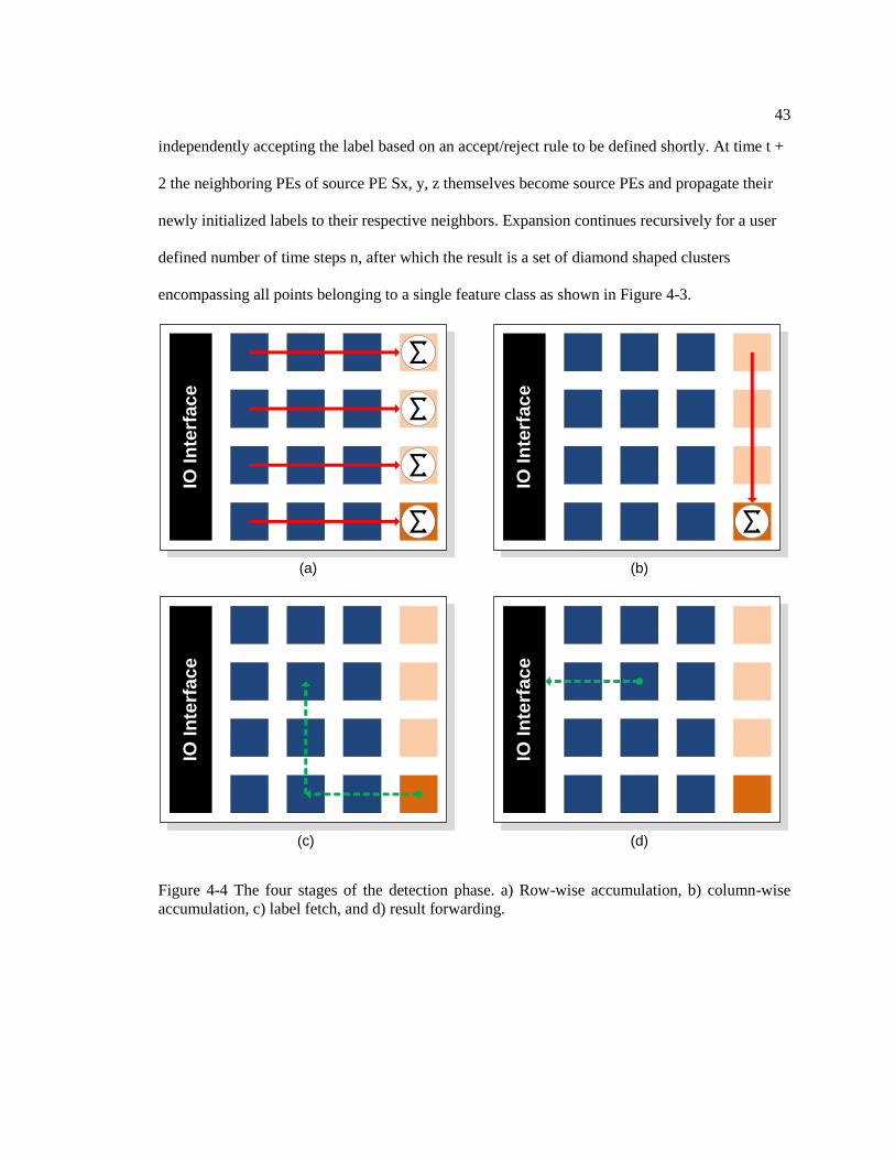
43
independently accepting the label based on an accept/reject rule to be defined shortly. At time t +
2 the neighboring PEs of source PE Sx, y, z themselves become source PEs and propagate their
newly initialized labels to their respective neighbors. Expansion continues recursively for a user
defined number of time steps n, after which the result is a set of diamond shaped clusters
encompassing all points belonging to a single feature class as shown in Figure 4-3.
IO In
terf
ac
e
(a)
IO In
terf
ac
e
(b)
IO In
terf
ac
e
(c)
IO In
terf
ac
e
(d)
Figure 4-4 The four stages of the detection phase. a) Row-wise accumulation, b) column-wise
accumulation, c) label fetch, and d) result forwarding.

44
Detection Phase
The detection phase is similar to the training phase except that sensors are periodically
interrogated and their accumulated responses transformed into indices into the classification array
previously trained. Figure 4-4 illustrates the detection process.
The online detection process is initiated periodically in the m x n array. The accumulation
of discretized sensor data is performed independently in each row by the m Row Aggregators,
RAs, in the right-most array column. Each PE propagates its local data towards the aggregators
at predefined intervals. Row-wise accumulation is performed for each of the three sensor types.
Following row-wise accumulation is column-wise accumulation performed by the bottommost
RA on behalf of the other m-1 RAs. The final accumulated values are mapped to equivalent x, y,
and z locations in the array by division efficiently implemented as right bit shifting. In addition a
Fetch Packet is generated for routing on the following cycle. Figure 4-4 (c) illustrates the routing
of a Fetch Packet towards a PE location addressed by the mapped aggregation results. As there
are m=n PEs in both x and y directions, the label fetch phase can take at most m+n cycles. Upon
arrival at the (x , y) destination, the Fetch packet is decoded by the PE and the z-location field
indexes into the Gas Label Register File, GLRF, to retrieve the correct label to be wrapped in the
RESULT PACKET. Retrieving the label and generating the fetch packet is performed in a single
cycle after which the RESULT PACKET is routed westward towards the IO interface. Because a
result is only forwarded westward the final result forwarding phase takes at most
n=number_of_columns cycles.
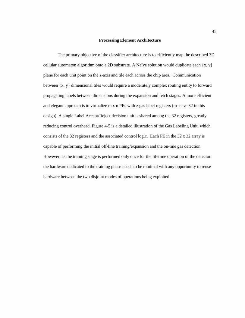
45
Processing Element Architecture
The primary objective of the classifier architecture is to efficiently map the described 3D
cellular automaton algorithm onto a 2D substrate. A Naïve solution would duplicate each {x, y}
plane for each unit point on the z-axis and tile each across the chip area. Communication
between {x, y} dimensional tiles would require a moderately complex routing entity to forward
propagating labels between dimensions during the expansion and fetch stages. A more efficient
and elegant approach is to virtualize m x n PEs with z gas label registers (m=n=z=32 in this
design). A single Label Accept/Reject decision unit is shared among the 32 registers, greatly
reducing control overhead. Figure 4-5 is a detailed illustration of the Gas Labeling Unit, which
consists of the 32 registers and the associated control logic. Each PE in the 32 x 32 array is
capable of performing the initial off-line training/expansion and the on-line gas detection.
However, as the training stage is performed only once for the lifetime operation of the detector,
the hardware dedicated to the training phase needs to be minimal with any opportunity to reuse
hardware between the two disjoint modes of operations being exploited.

46
Current Label
Distance Count
z-Location
Distance
Counter
Location
Counter
Up/Down
Load
Down
Load
Preset Count
Preset Count
Count
Count
Label Register
Label Register
Label Register
Label Register
Label Register
Label Register
Label Register
Label Register
Label Register
Label Register
Label Register
Label Register
Label Register
Label Register
Label Register
Label Register
Ad
dre
ss
De
co
de
r
Control
Unit
ENB
La
be
l S
ele
ct
DataIn[label]
DataIn[distance]
DataIn[z-location]
Clock
DataOut = Label
Propagate
Figure 4-5 Gas Labeling Unit
Operation
During the expansion stage a PE receives a packet from a neighboring PE and the
decision to accept the classification label at the specified z-location is made by the Control Unit
as follows: Location Counter, LC, is preloaded with the value of z-location and Distance Counter,
DC, is preloaded with the value of the distance attribute. The output of LC indexes into the Gas
Label Register File, GLRF, which causes a read of the existing contents of GLRF [LC]
(effectively GLRF [z-location]). At this point the Control Unit decides if the label will be written
into the register file based on the incoming label and incoming distance attribute and the existing

47
label and existing distance attribute. If the label will be accepted the Control Unit asserts the
propagate signal to allow propagation of the label to the nearest neighbors of the current PE on
the next clock cycle and asserts the ENB signal of the Address Decoder to allow the current label
to be written into the register file. After writing a label into the GLRF, LC is incremented and DC
decremented allowing the process to repeat for increasing register locations until either the
distance attribute reaches zero or the controller decides not to propagate further. The controller
begins expansion for decreasing GLRF locations starting from the original z-location by
reinitializing LC and DC with the original values of z-location and distance attribute. The
expansion process continues for all decreasing register locations starting from GLRF [LC]
(effectively GLRF [z-location]) until the distance attribute reaches zero or the controller decides
not to propagate a label further (i.e. the label is not accepted at the register in question).
Conclusion
The complete 8x8, fully parallel, PE array has been implemented in Verilog and
functional verified using cycle-accurate simulation. Table 4-1 shows device utilization of a
Xilinx Virtex-4 FX60 FPGA.
Table 4-1 Device Utilization
Resource Single PE Total ( 8x8 PEs) Total Device %
Slices 251 16,064 63 %
Registers 150 9,600 18 %
LUT 472 30,208 59 %
BlockRAM 1 64 27 %

Chapter 5
Framework for Hardware Accelerator Integration
While developing the architectures described in the previous three chapters it became
evident that in addition to implementing the functionality of a particular accelerator core, much of
the design effort was contributed to a number of reoccurring tasks: (1) designing interfaces to
system infrastructure components, and (2) developing custom state machines for controlling both
the micro operations and macro operations of the core.
System Infrastructure Interfaces
The first reoccurring aspect of accelerator design is the interface to system level
infrastructure and components such as memory and memory mapped devices. Tasks such as
creating interfaces to DDR2 memory controllers can take up to two weeks of design and
verification time. If an accelerator requires direct access to memory and memory mapped
devices, then a bus mastering controller must be implemented. Creating a bus master controller
for complex bus standards such as AMBA and PLB can take up to a week in design and
verification time. In addition, if the accelerator must be mapped into the memory space of the
system, then address bus decoding circuitry must be implemented. When software interaction is a
requirement, then a processor interface must be implemented which includes the design of
software register access logic, interrupt generation and clearing logic, and software debug
facilities. Each of these aspects requires intimate knowledge of the system bus employed for the
target platform, which increases verification effort dramatically (Goel & Lee, 2000). Though

49
industry standard busses such as IBM Processor Local Bus1, AMBA
2, and Wishbone
3 are widely
used, it is common for target platforms to adopt proprietary system communication protocols
which require non-standard interface design .
"Everyone has wanted a common on-chip bus to connect IP
[intellectual property]," said Ed McGettigan, senior systems engineering
manager at Xilinx. "Because [VSIA] has stalled, you see companies
coming out with their own bus standards."
The burden of creating these interfaces lie with the designer of the core: the interfaces
cannot, with any existing tool, be generated automatically by high-level synthesis tools. The
designer must be knowledgeable of all system infrastructure details and protocols, prohibiting
him/her from focusing, in isolation, on the design of the accelerator pipeline. Moreover, while
high-level synthesis tools may have been used to implement the accelerator pipeline, the skill of
the designer must be sufficient to manually implement many non-trivial system level interfaces.
In this chapter, I describe a framework that defines a contract between an accelerator core and the
target platform that abstracts the details of the system infrastructure into a concise set of standard
protocols and handshake interfaces.
Micro and Macro Operations
Micro Operations are the control sequences that dictate the cycle-by-cycle operation of
the internal pipeline of an accelerator core. This is similar to microcode, which is prevalent in
many moderate performance microcontroller and microprocessor implementations. Micro
1 Processor Local Bus (PLB) from International Business Machines (IBM)
2 Advanced Microcontroller Bus Architecture (AMBA) from ARM Holdings Ltd.
3 Open source bus highly in the OpenCores project.
50
Operations are typically static sequences that are tightly coupled with the control signals of the
pipeline and implemented as Finite State Machines. Contrarily, the high-level functionality of
many accelerators can be distinguished into one or more Macro Operations. For example, an FFT
accelerator may provide modes to perform 1-Dimensional FFT, Bit Reversal, and Image
Transpose. By appropriately scheduling these Macro Operations, FFT of any dimensionality can
be performed.
In a traditional design flow, Macro Operation sequences are implemented as state
sequencers within the accelerator hardware. Consequently, complex and/or variable operation
sequences involve designing large and highly complex control logic and state machines. One
solution to reduce the logic complexity of Macro Operations sequencers would be to provide an
interface for invoking the Macro Operations by software that executes on an embedded
microcontroller. Hardware complexity can be reduced by leveraging the ability of a
microcontroller to execute complex control flows that, in many cases, may exhibit dynamic
branching behavior. The penalty, of course, is suboptimal performance due to delays involved in
computing control branches between the completion of one Macro Operation and the invocation
of the next.
In this chapter, the design of a scalable algorithmic-level design framework for FPGAs,
AlgoFLEX, is described. AlgoFLEX offers rapid algorithmic level composition and exploration
while maintaining the performance realizable from a fully custom, albeit difficult and laborious,
design effort. The framework masks aspects of accelerator implementation, mapping, and
communication while exposing appropriate algorithm tuning facilities to developers and system
integrators. The effectiveness of the AlgoFLEX framework is demonstrated by rapidly mapping
a class of image and signal processing applications to a multi-FPGA platform.

51
FPGA Performance Benefits and Design Challenges
As FPGAs have migrated to lower technology nodes, their regular fabrics have allowed
them to improve their power-efficiency and computational capabilities at a rate exceeding general
purpose microprocessors or even custom ASICs [ (Underwood, 2004), (Cope, Cheung, Luk, &
Witt, 2005)]. While many of these benefits can be attributed to advances in CMOS process
technology, the ability for FPGAs to meet the performance requirements of complex signal
processing tasks has also been due to the inclusion of specialized components within the FPGA
fabric. These specialized components include multiply accumulate units, high speed transceivers,
internal memory, and embedded processors. Together these architectural enhancements allow
FPGAs to offer higher performance than a traditional “logic slice-only” fabric. For example, the
newly announced Virtex-6 devices from Xilinx include more than 1,000 embedded multiply
accumulate units supporting more than 1 Tera Multiply Accumulates (TMACs) per second. Such
performance profiles provide unique computational capabilities for compute intensive signal
processing algorithms. However, FPGAs face stiff competition from Graphical Processing Units
(GPUs) as the hardware platform of choice in signal processing applications due to the ease at
which GPUs can be programmed: an aspect in which FPGAs typically suffer (Cope, Cheung,
Luk, & Witt, 2005). Despite the lack of programmability, FPGAs hold several advantages over
GPUs in that FPGAs can be customized for specific numerical precisions, have the flexibility to
communicate with diverse I/O interfaces, and support customized control-intensive data
pipelines. Furthermore, FPGAs can provide better power-efficiency over GPUs due to the
customizable nature of the hardware. Unfortunately, if the usability and programmability issues
are not addressed, many of the performance benefits offered by FPGAs will remain unobtainable
for the general user.
52
A primary reason leading to the difficulty of FPGA design is the necessity to create (or
obtain) and integrate custom HDL IP cores in a fashion that results in a functionally correct
design that meets performance requirements. The first challenge lies with IP core creation itself,
where the design and validation difficulties are comparable to a custom ASIC implementation
and have high non-recurring engineering costs (NRE). Improving the NREs with core
development has been the focus of several commercial and academic efforts that attempt to
increase the abstraction of hardware design to high-level languages. For example, tools such as
ImplusC4, CatapultC
5, and Cameron
6 attempt to map high level algorithmic specifications in C
and C++ to HDL. Other tools, Calypto7 and the “Sequential Equivalence Checking Tool”
(Vasudevan, Viswanath, & Tu, 2006), attempt to map specifications provided in SystemC by
checking sequential equivalence of a system level model with an RTL version. Another effort is
Bluespec System Verilog which attempts to improve overall design time by reducing verification
times through strict type checking and a rule based language. Finally, there is AccelDSP8 from
Xilinx which uses MATLAB as input to generate HDL designs. While these tools ease the
generation of specific accelerator cores, they do not deal with the additional challenges associated
with system integration of several IP cores to make a complete system. To achieve this effect a
designer could use a combination of Simulink and Xilinx System Generator9, which provides a
graphical interface to permit system building through “plug n play” of different pre-defined
libraries. However handling dataflow is still a burden placed on the system designer. More
4 ImpulseC. The ImpulseC Web Page. [Online] 2007. http://www.impulsec.com
5 CatapultC. The Mentor Graphics Web Page. [Online] 2007.
http://www.mentor.com/products/esl/high level synthesis/catapult synthesis 6 Cameron: Compiling high-level programs to FPGA configurations. [Online] 2002.
http://www.cs.colostate.edu/cameron/ 7 Calypto‟s sequential analysis technology. [Online] 2008. http:// www.calypto.com/
8 AccelDSP. Xilinx AccelDSP Synthesis Tool. [Online] http://www.xilinx.com
9 Sysgen. The Xilinx Web Page. [Online] 2007.
http://www.xilinx.com/ise/optional prod/system generator.htm
53
recently, AccelDSP/System generator attempts to bring language based design flow into
consideration to improve the designer‟s experience.
This chapter introduces a comprehensive platform called AlgoFLEX, an FPGA based
development framework intended for application developers who want to use FPGAs for their
performance benefits, but do not possess the expertise of a seasoned hardware engineer. In order
to achieve this high-level of abstraction the AlgoFLEX platform adopts a methodology of
standardized interfaces and modular design across both hardware and software components. From
a hardware perspective, the platform provides standard interfaces to plug-n-play accelerator
modules, on-the-fly processing elements, and per accelerator programming primitives in order to
allow for run-time modification of and communication between, accelerators. With respect to
software, AlgoFLEX incorporates a graphical user interface for algorithmic specification and
Matlab style functional specification which support the generation of computational pipelines and
look-up table based kernel functions. Moreover, the framework allows for expandability by
providing additional facilities to expert users, allowing various components to be inserted at
multiple layers of abstraction. AlgoFLEX has been used in conjunction with two generations of
the BEE (2 and 3) multi-FPGA platforms to accelerate different image processing applications. In
particular, AlgoFLEX was used to map two types of re-gridding algorithms to the BEE platforms
and achieved performance comparable to a manual design flow while requiring a significantly
shorter design time.
Hardware Infrastructure
The AlgoFLEX hardware infrastructure, Figure 5-1, provides a system designer with the
capability to plug-n-play a collection of custom accelerator blocks without requiring intimate
knowledge of how those blocks will be composed. As shown, the platform consists of a hybrid

54
communication network comprised of a System Local Bus (SLB) and a packet-based on-chip
router along with memory controllers, accelerators, and other system components. While the SLB
serves as the communication backbone within a single FPGA, the router is used to coordinate a
secondary channel for both intra- and inter-FPGA communication. This communication is
primarily accomplished through the use of mailbox modules which provide messaging
capabilities between various tasks executing on different FPGAs. Moreover, mailboxes are the
principal mechanisms for ensuring proper dataflow between the tasks that are carried out on
different FPGAs. In particular, messaging and synchronization is accomplished by uniquely
binding a message to a task through the use of application-defined message identifiers. Upon
receiving an incoming message the mailbox module sends an interrupt signal to a microcontroller
which handles message interpretation for data synchronization. Once the appropriate handler has
been initiated, the message is decoded and one or more operations are triggered appropriately in
the hardware platform.
55
DDR2 MemoryDDR2 Memory
DDR2 Memory
Embedded
Microcontroller
SDRAM
Memory Controller
Custom Accelerator
Application Specific
Instruction Processor
Standard Bus Master Interface Standard Bus Slave Interface
Datapath
Control and
SynchronizationMemory
Bank 3
Memory
Bank 2
Memory
Bank 1
Memory
Bank 0
System Local Bus
Direct Memory
Access
and
Manipulate
(DMAM)
Mailbox
Router
Ethernet
Interface
Local
On-Chip
Memory
Interf-FPGA Interface
Figure 5-1 AlgoFLEX Hardware Infrastructure
In addition to custom accelerator modules, the AlgoFLEX infrastructure also allows for
the extension of the underlying base platform with negligible impact to the data flow and control
flow abstractions. For example, when migrating from the BEE2 to BEE3 platform, modifications
to the base platform were limited to the memory controllers and the inter-FPGA physical
interfaces: the remaining accelerator and mailbox components were not modified. The
adaptability of the platform is contributed to the modular design of two key computational
modules; the Direct Memory Access and Manipulate (DMAM) unit and the Universal Custom
Accelerator Module (UCAM).
56
Direct Memory Access and Manipulate
Write
Fifo
Write
Memory
Controller
Depacketizer
SLB Master
Interface 1
Read
Fifo
Packetizer
SLB Master
Interface 0
RX Stream
Operator n-1
RX Stream
Operator 1
RX Stream
Operator 0
TX Stream
Operator 0
TX Stream
Operator 1
TX Stream
Operator n-1
Read
Memory
Controller
TX XpressLink
Interface
RX XpressLink
Interface
SLB Slave
Interface
Command
Interface
TX
Xp
res
sL
ink
0
TX
Xp
res
sL
ink
1
TX
Xp
res
sL
ink
3
RX
Xp
res
sL
ink
0
RX
Xp
res
sL
ink
1
RX
Xp
res
sL
ink
3
Figure 5-2 Direct Memory Access and Manipulate pipeline architecture

57
The DMAM unit, shown in Figure 5-2, supports burst memory transactions, DMA
request initiation and packetizing/de-packetizing for on-chip and off-chip communications. In
addition to being the primary facility for transporting data throughout the system, the DMAM can
perform manipulations on data as it moves that data from source to destination. This is made
possible through the inclusion of application specific Stream Operators. Stream Operators are the
ideal implementation modality for common streaming operations including numerical conversion,
color space conversion, coordinate system conversion, data scaling, histogram computation,
vector differencing, and data binning. The DMAM also supports data specific manipulation,
where in the DMAM packetization phase appends qualifiers to data packets to signal the
appropriate Stream Operators to manipulate specific fields of a packet. Moreover, the DMAM
supports user defined coalescing and splitting of individual packets to minimize memory access
overhead and increase network transaction efficiency.
Figure 5-3 illustrates the DMAM Read Interface. Data transfer requests are enqueued at
the Command Interface via the System Local Bus, SLB, Slave Interface. The Read Memory
Controller parses commands and orchestrates data read transfers utilizing the SLB Master
Interface. Simultaneously, the Read Memory Controller configures the Packetize to packetize
and annotate the incoming data stream consistent with the specifications of the current command.
The asynchronous Read Fifo serves dual role as a data buffer as well as a clock domain
synchronizer, allowing the SLB Master Interface and the DMAM pipeline to operate in
independent clock domains. As data exits the Read Fifo, the Packetizer, as dictated by the
command, splits and/or replicates the incoming data stream into packets. Header information is
added to each packet to allow proper transport and manipulation through the following stages of
the DMAM pipeline.
58
Read
Fifo
Packetizer
SLB Master
Interface 0
Read
Memory
Controller
SLB Slave
Interface
Command
Interface
Word 6
Word 7
Header
Word 4
Word 5
Header
Word 2
Word 3
Header
Word 0
Word 1
Header
Memory
Word 0
Word 1
Word 2
Word 3
Word 4
Word 5
Word 6
Word 7
Figure 5-3 DMAM Read Interface
Figure 5-4 illustrates the DMAM Write Interface. As a packet enters the Depacketizer,
data write attributes such as store address and data length are extracted from the packet header.
The Depacketizer removes the header and forwards the remaining packet into the Write Fifo. The
asynchronous Write Fifo serves dual role as a Coalescing Data Buffer as well as a clock domain
synchronizer, allowing the SLB Master Interface and the DMAM pipeline to operate in
independent clock domains. The Coalescing facility allows separate yet related data packets to be

59
buffered and combined into larger data chunks that are more efficient to transfer across the SLB
Master Interface. Moreover, Watchdog timers ensure that coalesced data does not reside
indefinitely in the Write Fifo.
Write
Fifo
Write
Memory
Controller
Depacketizer
SLB Master
Interface 1
Memory
Coalesced Group 1 Word 2
Coalesced Group 1 Word 1
Coalesced Group 1 Word 0
Coalesced Group 0 Word 4
Coalesced Group 0 Word 3
Coalesced Group 0 Word 2
Coalesced Group 0 Word 1
Coalesced Group 0 Word 0
Word 0
Header
Word 1
Word 2
Header
Word 3
Word 4
Header
Word 5
Word 6
Header
Word 7
Figure 5-4 DMAM Write Interface
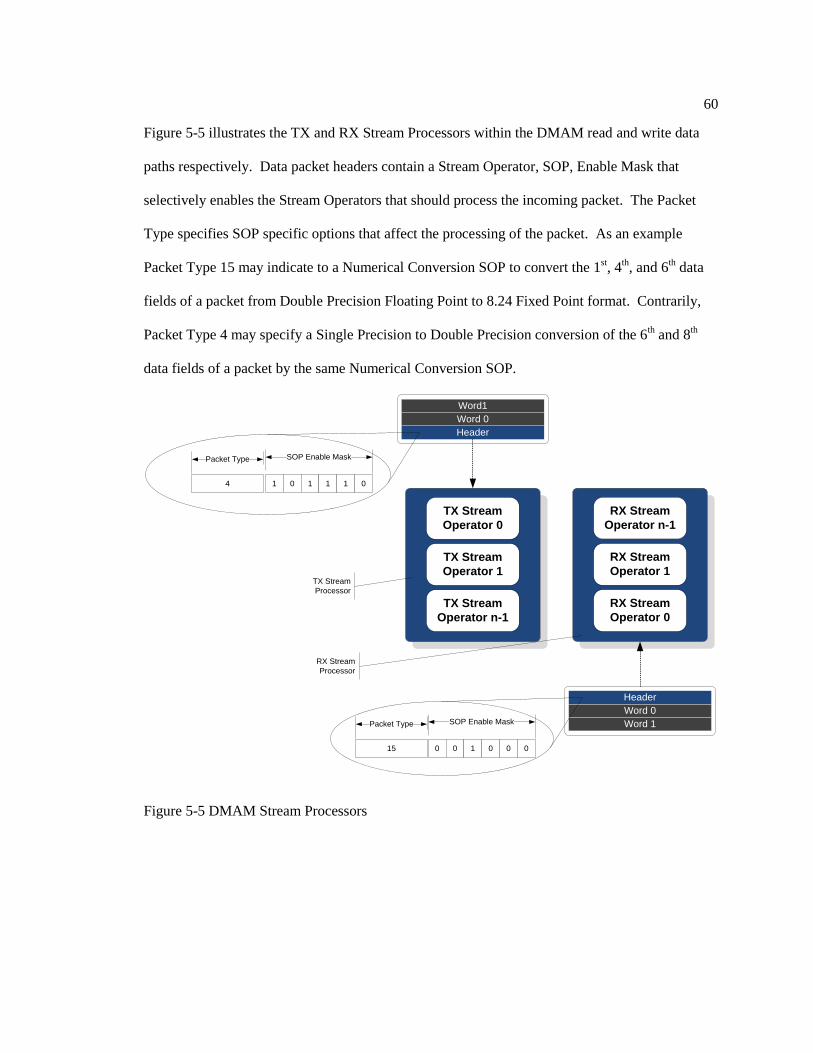
60
Figure 5-5 illustrates the TX and RX Stream Processors within the DMAM read and write data
paths respectively. Data packet headers contain a Stream Operator, SOP, Enable Mask that
selectively enables the Stream Operators that should process the incoming packet. The Packet
Type specifies SOP specific options that affect the processing of the packet. As an example
Packet Type 15 may indicate to a Numerical Conversion SOP to convert the 1st, 4
th, and 6
th data
fields of a packet from Double Precision Floating Point to 8.24 Fixed Point format. Contrarily,
Packet Type 4 may specify a Single Precision to Double Precision conversion of the 6th and 8
th
data fields of a packet by the same Numerical Conversion SOP.
RX Stream
Operator n-1
RX Stream
Operator 1
RX Stream
Operator 0
TX Stream
Operator 0
TX Stream
Operator 1
TX Stream
Operator n-1
Word 0
Word1
Header
Word 0
Header
Word 1
1 0 1 1 1 0
SOP Enable Mask
0 0 1 0 0 0
SOP Enable Mask
TX Stream
Processor
RX Stream
Processor
4
Packet Type
15
Packet Type
Figure 5-5 DMAM Stream Processors

61
Case Study: Streaming Skintone Detection in DMAM
Face localization refers to the machine vision process of locating human faces in an
image. To locate faces in an image a detection mechanism is applied at locations that have high
probability of containing a face. In general, detection mechanism only processes an image patch
that is substantially smaller than the entire input image. For example a particular detection
mechanism may be applied to 20 x 20 pixel subsets of the original 320pixel x 240pixel image. In
order to search the image for all possible locations of faces, assuming no prior knowledge about
the probability of existence of a face at a particular (x,y) location, the detector would be applied
starting at every (x,y) offset in the image.
Faces in an image can be found at a wide range of sizes. Normally the detection
algorithm is trained with faces of a fixed size: 20pixel x 20pixel for example. Consequently,
faces that exceed the dimensions of the Detection Window will not be detected. A solution to this
problem is to iteratively scale the image and perform detection at each distinct scale. Eventually
larger faces will be scaled to fit within the detection window. Even for a conservative number of
scales, exhaustively searching the image for faces can be prohibitive for real-time systems ( > 20
frames per second). Skintone detection solves this problem by filtering locations that would not
classify as faces because the tone of the pixels that comprise the detection window are not
representative of human skin.

62
Color Space
Conversion
RGB to YUV
Skintone
Detector
Streaming
Connected
Component
Processor
Performs conversion
between color
spaces utilizing a
streaming pipeline.
Scores pixels based
on a nonlinear
function of the YUV
channels. The score
measures closeness
to skintone.
Locates closed
regions of pixels
labeled as skintone.
Figure 5-6 Streaming Skintone Detection application mapped to Stream Operators in the Read
Stream Processor of a DMAM unit.
Figure 5-6 illustrates a pipeline of Stream Operators suitable for locating regions in an image that
have high likelihood of containing a human face. Each stream operator is fully pipelined with an
input and output rate of 1 datum/cycle.

63
Improved DMAM Architecture
One limitation of the DMAM engine discussed in the previous sections is that each data
packet flowing through the Stream Processor must traverse each Stream Operator in the pipeline.
Although each packet is annotated to selectively control whether a Stream Operator affects data
within the packet, every packet will experience the latency of every Stream Operator.
Second, although packets may require processing by mutually exclusive stream
operations, the rigidness of the DMAM pipeline illustrated in Figure 5-2 imposes dependencies
amongst otherwise independent packets. This is an artifact of the head-of-line blocking caused
by the single channel data path.
Third, the unidirectional dataflow of packets within a Stream Processor, Figure 5-5,
restricts the order and number of times a packet may visit a Stream Operator. In some cases it
there is utility in forwarding a packet through an arbitrary sequence of Stream Operators.
Figure 5-7 illustrates an improved DMAM architecture that addresses the aforementioned
limitations. The key feature of this architecture is that the data path between Stream Operators is
implemented as a high performance non-blocking switch. The switch allows packets to be routed
directly to appropriate Stream Operators bypassing others. Consequently, the best case latency
experienced by any packet is the sum of the latencies of each Stream Operator that the packet
must traverse. Though head-of-line blocking will occur, it will be minimal as the queues leading
into each Stream Operator will not enqueue all packets passing through the DMAM but rather
only those packets requiring manipulation by the particular Stream Operator.
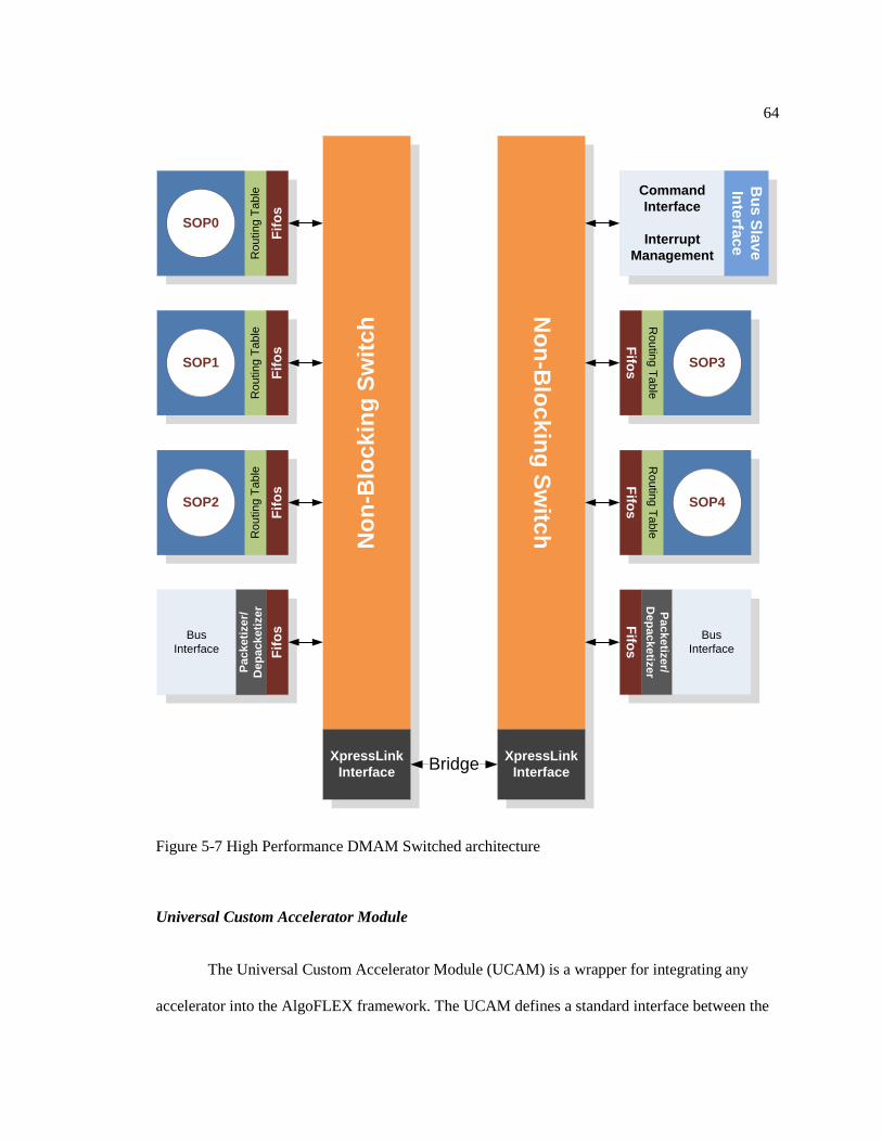
64
No
n-B
loc
kin
g S
wit
ch
No
n-B
loc
kin
g S
witc
h
Ro
utin
g T
ab
le
Fif
os
SOP0
Ro
utin
g T
ab
le
Fif
os
SOP1
Ro
utin
g T
ab
le
Fif
os
SOP2
Command
Interface
Interrupt
Management
Ro
utin
g T
ab
le
Fifo
s SOP3
Ro
utin
g T
ab
le
Fifo
s SOP4
Pa
ck
etiz
er/
De
pa
ck
etiz
er
Bus
Interface
Fifo
s
XpressLink
Interface
XpressLink
Interface
Bu
s S
lav
e
Inte
rfac
e
Pa
ck
eti
ze
r/
De
pa
ck
eti
ze
r
Bus
Interface Fif
os
Bridge
Figure 5-7 High Performance DMAM Switched architecture
Universal Custom Accelerator Module
The Universal Custom Accelerator Module (UCAM) is a wrapper for integrating any
accelerator into the AlgoFLEX framework. The UCAM defines a standard interface between the

65
built-in facilities and an instance of a specific accelerator hardware module. The functional
capabilities of the accelerator are exposed through the UCAM to any other UCAM compliant
accelerator in the system. AlgoFLEX allows the system to be composed of a number of
interconnected UCAM entities, with each UCAM offering custom acceleration to various parts of
an algorithm. Each of these UCAM accelerators can then be composed at a system level to
achieve the full functionality of the desired algorithm.
The UCAM design takes advantage of the fact that many signal processing applications
can be characterized by the following: 1) at the application level a sequence of subtasks are
repeatedly performed on incoming data and 2) the execution of subtasks consists of performing a
static set of compute intensive operations in a sequence that varies across any particular
invocation of the subtask. For example, an optimized Fast Fourier Transform (FFT)
implementation may selectively perform decomposition of data based on the dimensionality of
the data where 1-Dimensional FFT operations will be performed in all cases, but the sequence of
these operations may be radically different across different problem specifications. In the
AlgoFLEX framework both the application and subtask control can be implemented in software
on an embedded microprocessor, albeit with reduced system performance. To mitigate the
overhead of software orchestration of the accelerator‟s operations, the UCAM provides an
alternative hardware Command Fetch Unit that facilitates fetching, decoding, and preprocessing
of accelerator specific instruction sequences. These instruction sequences can be created and
modified as necessary for a particular invocation. Consequently, applications benefit from the low
overhead of direct hardware instruction fetching and decoding without the rigidness of a
hardcoded state machine.
In order to integrate a usable core into the AlgoFLEX framework, the designer of each
accelerator provides an HDL implementation that is compliant with the handshaking protocol and
signaling needed by the UCAM interface. Further, the designer of the module specifies the set of

66
primitive commands supported by the accelerator module. At a more abstract level, the algorithm
designer utilizes the module in different fashions by composing instruction sequences of primitive
commands.
Command
Fetch Unit
Window
Fetch
Handler
DMA
Handler
Custom
Handler 0
Custom
Handler
n-1
Command Ack
Bus Interface Module
Processor Command Valid
Processor Command
Processor Command Acknowledge
Processor Command Response
Application Specific Instruction
Processor (Internal View)
Cu
sto
m A
cce
lera
tor
Figure 5-8 Interface between UCAM and Custom Accelerator
Figure 5-8 illustrates the interface between the Application Specific Instruction Processor
(ASIP) and an accelerator core. The consumption of instructions is throttled through the UCAMs
handshaking protocol, allowing the accelerator to have fine grained control of the instructions
presented to it by the Command Fetch Unit. In a typical scenario, the Command Fetch Unit
fetches a command and dispatches it to an appropriate Command Handler module. The
Command Handler performs any instruction specific preprocessing before presenting the
command to the accelerator via the Processor Command bus along with the asserted Processor
Command Valid signal. If the accelerator core is available to process the command it will assert
the Processor Command Acknowledge signal along with any instruction specific response
information via the Processor Command Response bus.
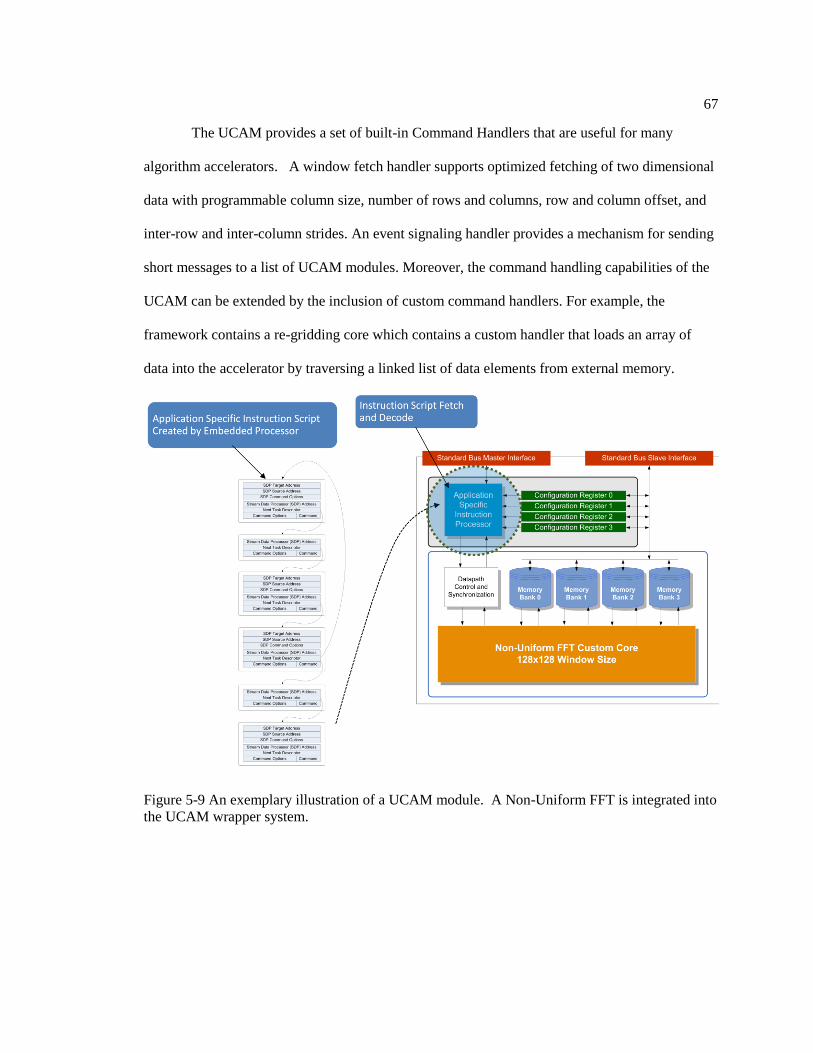
67
The UCAM provides a set of built-in Command Handlers that are useful for many
algorithm accelerators. A window fetch handler supports optimized fetching of two dimensional
data with programmable column size, number of rows and columns, row and column offset, and
inter-row and inter-column strides. An event signaling handler provides a mechanism for sending
short messages to a list of UCAM modules. Moreover, the command handling capabilities of the
UCAM can be extended by the inclusion of custom command handlers. For example, the
framework contains a re-gridding core which contains a custom handler that loads an array of
data into the accelerator by traversing a linked list of data elements from external memory.
Figure 5-9 An exemplary illustration of a UCAM module. A Non-Uniform FFT is integrated into
the UCAM wrapper system.
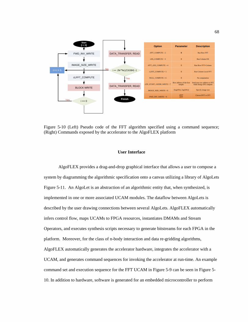
68
Start
[i = 0]
FWD_INV_WRITE
i == 0
i == (Nr*Nc)/(16384) -1
Finish
IMAGE_SIZE_WRITE
cLFFT_COMPUTE
BLOCK WRITE
DATA_TRANSFER, READ
DATA_TRANSFER, READ
i = i + 1
Yes
No
Yes
Option
rFFT_COMPUTE = 2
cDX_COMPUTE = 3
rFFT_cDX_COMPUTE = 4
cLFFT_COMPUTE = 5
NULL_COMPUTE = 6
cDX_START_rADDR_WRITE = 7
IMAGE_SIZE_WRITE = 8
FWD_INV_WRITE = 9
Parameter
0
0
0
0
0
Row address of the first sample.
{log2(Nc), log2(Nr)}
IFFTFFT
Description
Run Row FFT
Run Column DX
Run Row FFT+Column
Run Column Local FFT
No computation
Send start row address to FFT while doing cDX compute
Specify image size
Choose IFFT or FFT
Figure 5-10 (Left) Pseudo code of the FFT algorithm specified using a command sequence;
(Right) Commands exposed by the accelerator to the AlgoFLEX platform
User Interface
AlgoFLEX provides a drag-and-drop graphical interface that allows a user to compose a
system by diagramming the algorithmic specification onto a canvas utilizing a library of AlgoLets
Figure 5-11. An AlgoLet is an abstraction of an algorithmic entity that, when synthesized, is
implemented in one or more associated UCAM modules. The dataflow between AlgoLets is
described by the user drawing connections between several AlgoLets. AlgoFLEX automatically
infers control flow, maps UCAMs to FPGA resources, instantiates DMAMs and Stream
Operators, and executes synthesis scripts necessary to generate bitstreams for each FPGA in the
platform. Moreover, for the class of n-body interaction and data re-gridding algorithms,
AlgoFLEX automatically generates the accelerator hardware, integrates the accelerator with a
UCAM, and generates command sequences for invoking the accelerator at run-time. An example
command set and execution sequence for the FFT UCAM in Figure 5-9 can be seen in Figure 5-
10. In addition to hardware, software is generated for an embedded microcontroller to perform

69
initialization tasks such as configuring routing tables, performing memory allocation, and
memory mapping each UCAM. The executables for each microcontroller are loaded using a
JTAG debug interface while the system initialization data is loaded through an Ethernet interface.
AlgoLets: An AlgoLet is an
abstraction of an algorithmic entity
that, when synthesized, is implemented
in one or more associated UCAM
modules
AlgoLet
Library
System
Specification
Canvas
Figure 5-11 AlgoFLEX Graphical User Interface
Experimental Results
To demonstrate the flexibility of the AlgoFLEX framework, two different Re-gridding
algorithms were specified and synthesized by the system. The first re-gridding algorithm takes a
non-gridded 2D data set and maps it to a gridded 2D array using a Gaussian interaction kernel.
The second variant utilizes a B-Spline function as the interaction kernel. The designs were
targeted and executed on the BEE multi-FPGA platforms. Table 5-1 and Table 5-2 show the
performance of the resulting designs for different configurations of the re-gridding algorithms.

70
The subtle performance difference between the two architectures is due to the difference in
pipeline depth of the Gaussian and B-Spline kernels.
Table 5-1 Gaussian Kernel Interpolation
# of Source Points Target Grid Size Kernel Size Throughput frames/sec)
33600 512 x 512 4x4 55
33600 512 x 512 8x8 50
33600 512 x 512 12x12 35
Table 5-2 B-Spline Kernel Interpolation
# of Source Points Target Grid Size Window Size Throughput frames/sec)
33600 512 x 512 4x4 55
33600 512 x 512 8x8 49
33600 512 x 512 12x12 35
Conclusion
This chapter has presented a multi-FPGA acceleration platform developed as part of the
AlgoFLEX framework. While the results reported are for high-performance image processing
applications, the platform is also currently being used in low-cost embedded FPGA platforms.
Though the current version of the AlgoFLEX base platform libraries are targeted at the Xilinx
Virtex series of FPGAs, the architecture and platform can be easily ported to support other FPGA
targets.

Chapter 6
Conclusions
This dissertation discussed the benefits of using FPGA technology in classic and
emerging performance demanding application domains. Smart Sensing, Medical Imaging, and
Advanced Radar Processing were just a few applications that were shown to be dominated by
high computational complexity, diverse interface requirements, and low-power constraints. In the
context of these applications, the cost, size, and power advantages that FPGAs exhibit over
competing technologies such as Graphics Processing Units, GPUs, Application Specific
Integrated Circuits, ASICs, and standalone Digital Signal Processors, DSPs, were highlighted.
Moreover, shown were the challenges related to FPGA design and usability that prohibit
algorithm implementers that are neither hardware engineers nor experts in digital design from
utilizing and benefitting from FPGA technology. Issues pertaining to algorithmic level
programmability of FPGAs and their implications for the future adoption of FPGAs as viable
computing platforms were presented.
Towards resolving the challenges of implementing common image and sensor
processing algorithms on FPGA, this dissertation contributes high performance hardware
architectures and implementations for three commonly used classification algorithms.
Specifically, Chapter 2 illustrated an efficient Support Vector Machine implementation that
utilized novel Gaussian Kernel evaluation optimizations in tandem with embedded DSP resources
available in all current-day FPGA fabrics.
Chapter 3 presented a streaming artificial neural network design, which performs both
face detection and gender recognition simultaneously on a real-time video stream. Again, the

72
architecture makes judicious use of embedded FPGA resources including DSP48 Multiply and
Accumulate tiles and True Dual Port BlockRAMs found in Xilinx Virtex-4 series of FPGAs.
Chapter 4 contributed a novel implementation for a nanosensor based gas detection
system. In particular, hardware virtualization techniques were employed to map a 3-Dimensional
Nearest Neighbor Classifier onto a 2-Dimensional FPGA fabric. Other key aspects of the
architecture included hardware reuse across the training and detection modes of operation and a
completely distributed processing array.
Finally, Chapter 5 introduced AlgoFLEX, a unified framework for rapid integration of
accelerator cores into a system that may span many FPGA devices. By removing many of the
redundant and time consuming tasks of integrating an accelerator such as creating memory and
bus interfaces, AlgoFLEX reduces the design skills necessary for an algorithm implementer to
effectively utilize FPGA technology. Moreover, AlgoFLEX removes many of the hurdles related
to system level infrastructure that prohibit the total automation of system design and
implementation. Consequently, AlgoFLEX makes the abstraction of FPGA design more familiar
to algorithm implementers who generally program in high level languages such as C and C++.
Future directions of this work include leveraging Dynamic Partial Reconfiguration, DPR,
technology that will be prevalent in future FPGA devices. Through virtualization of hardware
resources and functionality over time and device space, DPR affords applications the benefits of
platforms that have virtually limitless capacity for hosting accelerators. Moreover, DPR makes
possible the intriguing notion of moving computation to data. In this computation model,
relatively small bitstreams that represent complex hardware accelerators can be migrated to the
data that needs to be manipulated by those accelerators. A direct consequence is a reduction in
I/O bandwidth requirements necessary for transporting large datasets across memory hierarchies
and bus interfaces to the location of computation accelerators. Both the DMAM and UCAM

73
components discussed in Chapter 5 can easily be adapted to support this novel model of
computation.
Works Cited
Anderson, K. F. (1998). Your Successor to the Wheatstone Bridge? NASA's Anderson
Loop. IEEE Instrumentation and Measurement Magazine .
Burges, C. J. (1998). A Tutorial on Support Vector Machines for Pattern Recognition.
Data Mining and Knowledge Discovery , 121-167.
Cope, B., Cheung, P. K., Luk, W., & Witt, S. (2005). Have GPUs made FPGAs
redundant in the field of video processing? Proceedings of the IEEE International Conference on
Field Programmable Technology, (pp. 111-118).
Frost. (2007, October 31). FPGA, DSP, ASIC Growth Driven by Demand for Flexibility
in Medical Imaging Equipment. Retrieved 2 20, 2009, from Frost & Sullivan:
http://www.frost.com/prod/servlet/report-analyst.pag?repid=N1CF-01-00-00-00
Goel, A., & Lee, W. R. (2000). Formal Verification of an IBM CoreConnect processor
local bus arbiter core. Proceedings of the 37th Annual Design Automation Conference (pp. 196-
200). Los Angeles: 2000.
IBM. (2007). 128-Bit Processor Local Bus Architecture Specifications. IBM.
Irick, K. M., Theocharides, T., N., V., & Irwin, M. J. (2006). A Real Time Embedded
Face Detector on FPGA. Asilomar Conference on Signals, Systems, and Computers. Pacific
Grove.
Li, J., Papachristou, C., & Shekhar, R. (2005). An FPGA-based computing platform for
real-time 3D medical imaging and its application to cone-beam CT reconstruction. Journal of
Imaging Science and Technology , 237-245.
Melnikoff, S. J., & Quigley, S. F. (2003). Implementing log-add algorithm in hardware.
IEE Electronics Letters , 939-940.

75
Miner, G. F., & Comer, D. J. (1992). Physical Data Acquisition for Digital Processing.
Englewood Cliffs: Prentice Hall.
Mitsubayashi, K., Matsunaga, H., Nishio, G., Ogawa, M., & Saito, H. (2004).
Biochemical gas-sensor (bio-sniffer) for breath analysis after drinking. SICE 2004 (pp. 97-100).
IEEE.
Moreland, K., & Angel, E. (2003). The FFT on a GPU. SIGGRAPH/Eurographics
Workshop Graphics Hardware, (pp. 112-119).
P. G. Tzionas, P. G. (1994). A New, Cellular Automaton-based, Nearest Neighbor Pattern
Classifier and its VLSI Implementation. IEEE Transactions on Very Large Scale Integration ,
343-353.
Potts, D., Steidl, G., & Tasche, M. (2001). Fast Fourier transforms for nonequispaced
data: A tutorial. In Modern Sampling Theory: Mathematics and Applications (pp. 247-269).
Birkhauser Boston.
Rowley, H. A., Baluja, S., & Kanade, T. (1998). Neural Network-Based Face Detection.
IEEE Transactions On Pattern Analysis and Machine Intelligence , 39-51.
Roy, N. (2006, July 1). Picture this: FPGAs in medical imaging. Retrieved 12 14, 2008,
from DSP-FPGA.com: http://www.dsp-fpga.com/articles/id/?1865
Schiwietz, T., Chang, T., Speier, P., & Westermann, R. (2006). MR Image
Reconstruction Using the GPU. SPIE, (pp. 1279-1290).
Sinesio, F., Natale, C. D., Quaglia, G. B., Bucarelli, F. M., Moneta, E., Macagnano, A., et
al. (2000). Use of electronic nose and trained sensory panel in the evaluation of tomato quality.
Journal of the Science of Food and Agriculture , 63-71.
Smith, P. A., Nordquist, C. D., Jackson, T. N., Mayer, T. S., Martin, B. R., & Mbindyo, J.
(2000). Electric-field assisted assembly and alignment of metallic nanowires. Applied Physics
Letters , 1399.
76
Stone, S., Haldar, J., Tsao, S. C., Hwu, W.-m., Liang, Z.-P., & Sutton, B. P. (2008).
Accelerating Advanced MRI Reconstructions on GPUs. Proceedings of 5th International
Conference on Computing Frontiers.
Sumanaweera, T., & Liu, D. (2005). Medical image reconstruction with the FFT. In GPU
Gems II (pp. 765-784). Addison Wesley.
Swartzlander, E. E., & Alexopoulos, A. G. (1975). The Sign/Logarithm Number System.
IEEE Transactions On Computers , 1238-1242.
Sweeney, L., & Gross, R. (2005). Mining Images in Publicly-Available Cameras for
Homeland Security. AI Technologies for Homeland Security.
Underwood, K. (2004). FPGAs vs. CPUs: Trends in Peak Floating Point Performance.
Proceedings of the International Symposium on Field Programmable Gate Arrays.
Valleron, A., Pijolat, C., Viricelle, J.-P., Breuil, P., Marchand, J.-C., & Ott, S. (2009).
Exhaust Gas Sensor Based on Tin Dioxide for Automotive Application. International Symposium
on Olfaction and Electronic Nose, (pp. 450-451).
Vasudevan, S., Viswanath, V., & Tu, J. (2006). Automatic decomposition for sequential
equivalence checking of system level and RTL descriptions. Proceedings of International
Conference on Formal Methods and Models for Co-Design, (pp. 71-80).
Volder, J. E. (1959). The CORDIC Trigonometric Computing Technique. IRE
Transactions On Electronic Computers .
Wang, J. (2009, May 19). What Are Your Customers Thinking? Retrieved May 20, 2009,
from Entrepreneur: http://www.entrepreneur.com/technology/newsandtrends/article201702.html
Williams, D. E., & Pratt, K. F. (1996). Resolving combustible gas mixtures using gas
sensitive resistors with arrays of electrodes. Journal of the Chemical Society, Faraday
Transactions , 4497-4504.

77
Wiskott, L. (2004). How Does Our Visual System Achieve Shift and Size Invariance? In
J. L. van Hemmen, & T. J. Sejnowski, Problems in Systems Neuroscience. Oxford University
Press.
Xu, F., & Mueller, K. (2005). Accelerating Popular tomographic reconstruction
algorithms on commodity PC graphics hardware. IEEE Transactions on Nuclear Science , 654-
663.
Xu, W., N., V., Xie, Y., & Irwin, M. J. (2004). Design of a Nanosensor Array
Architecture. ACM Great Lake Symposium on VLSI.
Xue, X., Cheryauka, A., & Tubbs, D. (2006). Acceleration of fluoro-CT reconstruction
for a mobile C-Arm on GPU and FPGA hardware: a simulation study. SPIE, (pp. 1494-1501).

VITA
Kevin Maurice Irick
Ph.D. in Computer Science and Engineering, Department of Computer Science and Engineering, The Pennsylvania
State University, University Park, PA. Major field: Application Specific Hardware. Research interests: machine vision,
FPGA acceleration, computer aided design, application specific embedded systems. Dissertation: A Configurable
Platform for Sensor and Image Processing. Chair: Professor Vijaykrishnan Narayanan. August, 2009
Master of Science, Computer Science and Engineering, The Pennsylvania State University, University Park, PA.
Professional specialization: Pattern Recognition Accelerators on FPGA. Master‟s Thesis: Embedded Face Detection.
May, 2006
Bachelor of Science, Electronics Engineering Technology, DeVry University, Decatur, Ga. June 2002
Irick, K. M., DeBole, M., Narayanan, V., & Gayasen, A. (2008). A Hardware Efficient Support Vector Machine
Architecture for FPGA. Proceedings of the 2008 16th International Symposium on Field-Programmable Custom Computing Machines
(pp. 304-305). IEEE Computer Society.
Irick, K. M., DeBole, M., Narayanan, V., Sharma, R., Moon, H., & Mummareddy, S. (2007). A Unified Streaming
Architecture for Real Time Face Detection and Gender Classification. Proceedings of the 2007 International Conference on Field
Programmable Logic and Applications, (pp. 267-272). Amsterdam.
Irick, K. M., Xu, W., Narayanan, V., & Irwin, M. J. (2005). A Nanosensor Array-Based VLSI Gas Discriminator.
Proceedings of the 18th International Conference on VLSI Design (pp. 241-246). IEEE Computer Society.
Irick, K., DeBole, M., Park, S., Maashri, A., Kestur, S., Yu, C.-L., et al. (2009). A Scalable Multi-FPGA Framework for
Real-Time Digital Signal Processing. SPIE: Photonics, Optics, & Imaging.
Irick, K., Theocharides, T., Narayanan, V., & Irwin, M. J. (2006). A Real Time Embedded Face Detector on FPGA.
Proceedings of the Fortieth Asilomar Conference on Signals, Systems and Computers, (pp. 917-920).
Kim, J. S., Deng, L., Mangalagiri, P., Irick, K., Sobti, K., Kandemir, M., et al. (2009). An Automated Framework for
Accelerating Numerical Algorithms on Reconfigurable Platforms Using Algorithmic/Architectural Optimization. IEEE Transactions
on Computers .
Kim, J., Mangalagiri, P., Irick, K. M., Kandemir, M., Narayanan, V., Sobti, K., et al. (2007). TANOR: A Tool for
Accelerating N-Body Simulations on Reconfigurable Platform. Proceedings of the 2007 International Conference on Field
Programmable Logic and Applications, (pp. 68-73). Amsterdam.
Ricketts, A. J., Irick, K. M., Narayanan, V., & Irwin, M. J. (2006). Priority Scheduling in Digital Microfluidics-Based
Biochips. Proceedings of the 2006 Design, Automation and Test in Europe, (pp. 1-6). Munich.
Theocharides, T., Nicopoulos, C., Irick, K. M., Narayanan, V., & Irwin, M. J. (2008). An Exploration of Hardware Architectures for
Face Detection. In The VLSI Handbook of Signal Processing.