a code warrior’s guide to microcontrollers
DESCRIPTION
Microcontrollers guideTRANSCRIPT

A Code Warrior’s Guide to Microcontrollers
Programming the Freescale HCS12
Warren A. Rosen, Ph.D. Engineering Technology Program Drexel University

2
Preface
Dear Reader,
This is a book about microcontrollers. Microcontrollers rule the world when we aren’t looking. They run our cars, trains and planes, medical devices, our kitchen appliances, our telephones, printers, robots, and about a zillion other things that we’re not aware of. There’s even a microcontroller inside the battery in the laptop I’m typing this on, and probably yours, too. There are billions of them in use today and they do their job ceaselessly and without complaint for years at a time (at least for the most part).
Applications such as those just mentioned are examples of what are known as “embedded systems.” These are systems designed to turn on when you push the power button, do their job without intervention from you, and then turn off when you push the button again. The microcontroller is buried deep inside these systems and you never see it. Microcontrollers are also used around the world by artists and hobbyists to make animated art, toys, robots, or just flashing lights for the fun of it.
A microcontroller is similar in some ways to a microprocessor (in fact, it has a microprocessor contained inside it) and dissimilar in others. The biggest difference is that they are “systems-on-a-chip,” that is, they usually have everything on a single integrated circuit needed to sense and control the outside world. Also, they usually run a lot slower than the microprocessor in your laptop or desktop. This keeps the power and cost down, and many of them cost less than a dollar. Power is important because they are often used in battery-powered autonomous operations.
In this course you will learn what’s inside a microcontroller and how they do their job. You will also learn how to program them to do all sorts of useful and fun things.
A note about the text—this is the first edition, and it may have many errors, both small and big. If you spot any, don’t hesitate to let me know; you may make it into the Acknowledgements if there is ever a second edition.
3
Table of Contents
Table of Contents ............................................................................................................................................... 3
Chapter 1. Introduction .................................................................................................................................. 5 Number Systems ........................................................................................................................................................... 5 Introduction to Microcontrollers ........................................................................................................................ 13 What Goes on Inside a Microcontroller ........................................................................................................... 15 What You Need to Know to Program a Microcontroller ........................................................................... 19 Instant Quiz Answers ............................................................................................................................................... 22 Homework .................................................................................................................................................................... 22 References .................................................................................................................................................................... 23
Chapter 2. Programming the Microcontroller ................................................................................... 24 Programming languages ......................................................................................................................................... 24 The CodeWarrior IDE .............................................................................................................................................. 25 Some Useful Instructions ....................................................................................................................................... 25 Some Useful Assembler Directives .................................................................................................................... 34 Instant Quiz Answers ............................................................................................................................................... 36 Homework .................................................................................................................................................................... 38
Chapter 3. I/O Ports ...................................................................................................................................... 39 Parallel I/O Ports ....................................................................................................................................................... 41 An Example: Process Control Automation ..................................................................................................... 44 Instant Quiz Answers ............................................................................................................................................... 50 Homework .................................................................................................................................................................... 51
Chapter 4. Indexed Addressing ................................................................................................................ 52 Instant Quiz Answers ............................................................................................................................................... 59 Homework .................................................................................................................................................................... 59
Chapter 5. Assembly Directives ................................................................................................................ 61 Shift Operations .......................................................................................................................................................... 67 Some Useful Assembly Directives ...................................................................................................................... 71 Assembly Expressions ............................................................................................................................................. 77 Instant Quiz Answers ............................................................................................................................................... 79 Homework .................................................................................................................................................................... 80
Chapter 6. Timing and Pulse Width Modulation ............................................................................... 82 The HCS12 Timing Module .................................................................................................................................... 87 The HCS12 Pulse-‐Width Modulation Module ................................................................................................ 92 Instant Quiz Answers ............................................................................................................................................... 97 Homework .................................................................................................................................................................... 98
Chapter 7. Interrupts .................................................................................................................................... 99 What are Interrupts and how do They Work? .............................................................................................. 99 What happens when an interrupt occurs? ................................................................................................... 101 The WAI Instruction ............................................................................................................................................... 107 Instant Quiz Answers ............................................................................................................................................. 109

4
Homework .................................................................................................................................................................. 109 References .................................................................................................................................................................. 110

Chapter 1. Introduction
In this chapter we’ll discuss three topics. The first is that of number systems used by microcontrollers and the development software used to program them. Next, we’ll describe what a microcontroller is, what they’re used for, and the differences between a microcontroller and a microprocessor. We’ll conclude with what is called the microcontroller “organization.” This is a description of how the internal components (central processing units, memory, etc.) are organized (what is connected to what), a description of special registers inside the microcontroller used for things such as doing arithmetic, the instruction set (a description of what instructions the microcontroller can perform, such as “add two numbers together), and the memory map, which is a graphical description of the memory in terms of which addresses in the memory are used to perform what special functions (for example, where is the program or the data stored).
Number Systems Microcontrollers, like microprocessors, operate at the physical level using binary numbers
represented by physical voltage levels, so we have to understand binary numbers in detail. We can understand how binary numbers work by remembering how ordinary decimal numbers work. For example, in Figure 1-1, the number 124.375 (base 10), the 4 to the left of the decimal point represents the number of ones (100), 2 represents the number of tens (101), and the leftmost 1 the number of hundreds (102). Note that 10 is the base, which means the digits run from 0 to the base minus 1 (9).
Figure 1-1. How a number is represented in the decimal number system.
Binary numbers form a natural system for representing data in modern computers. In the binary number system the base is 2 and the digits go from 0 to 2 minus 1, that is, they’re just 0 and 1, so you can represent them with just two voltage levels, 0 V for logical 0 and something like 1.8, 3.3, or 5 V for logical 1.
For example, in the number 1111100.0112 the first number to the left of the decimal point (actually the “binary point” or, in general, the “radix point”) is the number that multiplies 20, the next multiplies 21, and so on, as shown in Figure 1-2. The first number to the right of the binary point multiplies 2-1 = 1/2, the next 2-2 = 1/4, and so on.

6
This number, then, is equal to 1x26+1x25+…+0x21+0x20+0x2-1+1x2-2+1x2-3, which is equal to 124.37510, which is the same number in Figure 1-1.
Figure 1-2. Representation of a number in the binary system.
Most microcontrollers (and microprocessors, too) operate in multiples of 8-bit symbols called “bytes.” Sometimes it’s useful to use 4-bit symbols, or half a byte. Naturally, half a byte is called a “nibble.”
Arithmetic Addition is done the same way as with decimal numbers. For example, suppose you want to
add 5810 + 1710 = 7510. In binary this would be 0011 00111010 (=5810) +00010001 (=1710) 01001011 (=7510) The numbers in red are the “carry” bits. For example, in the fourth column from the left, the
sum is 1 + 1 = 0, “carry the two (the first red bit on the right). The most significant carry bit (the zero on the extreme left) is important. The reason is that,
while on a piece of paper you can add numbers of as many bits as you like, the processor only has storage space for a finite number of bits. For example, suppose you wanted to add the two 8-bit numbers below using a processor that stores results as 8-bit bytes.
1011 10111010 +10010001 101001011 On paper you can just write down the leftmost carry bit next to the zero in the answer, as
shown, but in the processor the answer would be truncated to 8 bits. To deal with this problem the processor keeps track of special bits like the carry (or C) bit in
a special register called the Condition Code Register, or CCR. We’ll talk about some of the other bits in the CCR in a while.

7
Subtraction Doing subtraction in a processor is an interesting problem. On paper when you want to do
subtraction, you just put a little minus sign in front of the number you want to subtract. This converts it to a negative number. In a processor there’s no place to put a minus sign, just ones and zeros. To deal with this problem, most processors represent negative numbers using what is known as Two’s Complement Arithmetic.
To get the two’s complement of a number, you first complement it (change all the 1s into 0s and all the 0s into 1s) and add 1 to the result. (The complement, before adding 1, is called the one’s complement.)
As an example, let’s find the two’s complement of the number 0510. In binary
0510 = 00000101, so the one’s complement is
05 = 11111010. To get the two’s complement, add 1 to this in the normal way you do addition
11111010 +00000001
-05 = 11111011. If you don’t believe this is -5, just add +5 to it to see what you get:
1 -05 = 11111011 +05 = 00000101 00000000.
So we get all zeros, plus a carry out. The carry bit isn’t part of the answer; it’s just stored in the CCR in case we need to pay attention to it.
By the way, this is how a computer does subtraction using two’s complement—it just converts the second number to its two’s complement and adds the result to the first number.
Note that in the two’s complement representation for -5 the most significant bit is a 1. This is a common feature of two’s complement negative numbers—all negative numbers begin with one. This means that the magnitude of the number is represented by the remaining 7 bits. This, in turn, means that an 8-bit two’s complement number can represent the numbers -128 (10000000) through +127 (01111111).
Instant Quiz (the answers are at the end of the chapter, but try doing them yourself first, before looking)
1. Convert the following decimal numbers to 8-bit binary: a) 33 b) -33
2. Add the following two binary numbers: 00010011 + 11101101.

8
3. Perform the following binary subtraction: 00111111 – 01001100. (Just convert the second number to it’s two’s complement and add.) Is the result positive or negative?
The Overflow Problem So far, so good—we can do addition and subtraction just like a computer, but there’s a
problem. It’s called the “overflow” problem and it’s associated with the problem of truncation that we just talked about.
Here’s an example of how it works: Suppose you want to add the numbers 64 + 65. In binary it’s just
01 64 = 01000000 +65 = +01000001 10000001 ,
but the binary answer is -127, not 129!!! Here’s another example—add -64 to -65:
10 -64 = 11000000 - 65 = +10111111 01111111 ,
and the binary answer is +127 instead of -129!!! The problem in the top example is that there has been a carry into the 7th (most significant)
bit but no carry out, making the answer incorrectly look negative (note that we number the bits starting with 0, from 20). In the bottom example there has been a carry out of the 7th bit but no carry in, making the answer incorrectly look positive. This is the overflow problem.
Microcontrollers (and microprocessors, too) handle this problem by flagging it in a “V” bit. If the two carry bits in each of the examples above are the same, V=0; if they’re different, V=1. The V bit is stored in the CCR, along with the C bit. Notice that making V = 0 if the two carries are the same and 1 otherwise is equivalent to saying that the V bit is the Exclusive-OR of the two carry bits.
Instant Quiz
4. Find the value of the V bit for Quiz Question 3, above. In addition to the C and V bits, microcontrollers and microprocessors keep track of a number
of other useful “status” bits. The microcontroller you will be using, the Freescale HCS12, tracks eight of these in the CCR. These are the following
C (carry/borrow) = 1 if carry occurs during addition or minuend < subtrahend during subtraction

9
V (overflow) = 1 if a 2’s complement overflow occurred (two most significant bits of the carry word are different)
Z (zero) = 1 if result is zero N (negative) = 1 if MSB of result is set (=1)
I = interrupt mask H = half carry
X = X interrupt mask S = stop disable
The Carry bit actually plays a double role. In addition it acts the way you would think, but in subtraction it acts as a “Borrow” bit. Here’s how it works: in addition you just look at the most significant carry bit; if it’s 1 the C bit equals 1. If it’s 0 the C bit equals 0. However, if you’re dong subtraction, if the bottom number is bigger than the top number, C = 1, if it’s less, C = 0.
Let’s do an example, 15 – 5: 11111 111 0000 1111 (15) + 1111 1011 (-5) 0000 1010 (10)
Notice that we’re subtracting 5 by adding -5 (i.e., the two’s complement of +5 that we found before). So, what is the value of the C bit? Well, you might think it’s 1 because the most significant carry bit (in red) is 1, but you’d be wrong. Remember, this is subtraction, so you don’t look at the carry bits. Instead, you just ask if the bottom number is bigger that the top number. 5 is less than 15, so C = 0.
The V bit for the example above is 0, because the two most significant carry bits are the same (both 1).
Next are Z and N. The Z bit answers the question, did the last thing (instruction) the processor do result in a zero. If yes, the Z bit is 1 (true). If not, it’s 0 (false). This turns out to be a handy thing to know. Suppose you’re counting some events (e.g., pulses from some external sensor) and you want to know when you’ve counted to 100. The obvious way to do this in the microcontroller is to start with zero, then at the first event add 1, at the next event add one to that, and so on, each time comparing your sum to see if you got to 100. The comparing function takes some time because you have to do the addition, then fetch the number you’re comparing the result to (100) and then compare the two. A faster way would be to start at 100 and count down. When you get to zero the Z bit goes high (=1) automatically, and you know right away that you’ve counted 100 events, without doing any additional fetching or comparing. This is such a useful tool that there are a lot of instructions that do something if Z = 0, and a lot more that do something if Z = 1.
The N bit is equal to one if the last thing you did resulted in a negative number (i.e., the most significant bit of the result is 1).
The I and X bits are used in interrupts. An interrupt is an unscheduled event that causes the microcontroller to stop its normal operation and do something else for a while. As an example,

10
suppose your microcontroller is taking and analyzing data from some sensors but you also have a smoke detector attached to an interrupt pin. You can set the microcontroller up so that it runs the normal data acquisition program but if it gets an interrupt signal it stops and turns on a sprinkler system and alarm bell. We’ll talk more about the I and X bits in a later chapter.
The half carry bit, H, does the same thing as the C bit but just for addition and subtraction of nibbles (4-bit symbols).
Finally, the S bit enables or disables the Stop instruction. This instruction, as the name implies, stops the processor from running.
Before moving on, when we talked about the Z and N bits, we said that they indicate whether the last operation resulted in a zero or negative number. This isn’t completely true; some operations don’t affect these bits. What we really meant was that they are determined by the last relevant operation. If, for example, we add numbers together, or load or store them somewhere, the bits can change, but there are some operations that don’t affect them. We have to be a little careful. In a few chapters we’ll see how to find out if a particular operation affects the Z and N bits. In the meanwhile, it’s time for a quick quiz. Instant Quiz
5. What are the values of the Z and N bits for the example above (15 – 5)?
Hexadecimal Numbers As you can see, it’s difficult for us to read and calculate with long strings binary numbers. As
a result, instructions and data are often represented in hexadecimal (base 16). Of course, the processor still uses binary 1s and 0s; hexadecimal is just an easy way for us to deal with them.
Just as in decimal the digits run from 0 to 9 and in binary they run from 0 to 1, in base 16 they run from 0 to 15. The first 9 digits are just 0 to 9, but then 1010 is represented by A16, 1110 by B16, 1210 by C16, and so on, up to 15, represented by F16.
For example, for the hexadecimal number 7C.616:
7C.616 = 7 x 161 + 12 x 160 + 6 x 16-1, which adds up to 124.37510, the same number as in Figure 1-1 and Figure 1-2.
We should note that what happens to the right of the decimal point doesn’t always convert so easily. For example, if we wanted to convert 124.110 to binary we would get
124.110 = 01111100.00011001100110011001100110011001…, and in hex
124.110 = 7C.19999999999999999…, so we would need an infinite series to represent the 0.1.
It’s easy to convert back and forth between binary and hexadecimal. To go from binary to hex, just divide the binary number into groups of 4-bit nibbles, starting on the right and working left, and then just convert each nibble into its corresponding hexadecimal digit. For example,

11
11100011 = 1110 0011 = E3. E 3
To go from hex to binary just reverse the process and convert each hexadecimal digit to its 4-
bit binary equivalent. So, for example 2F = 00010 1111 = 00101111. 2 F Here’s another example. Suppose you have a processor with a 16-bit address bus. The largest
memory address you could address is the one in which the bits are all 1s: M = 11111111111111112 = 1111 1111 1111 11112 = FFFF. F F F F
In decimal, this is
FFFF = 15 x 163 + 15 x 162 + 15 x 161 + 15 x 160 = 65,53510. This is nominally called a “64K address space.”
Instant Quiz
6. Convert FF16 to binary, and 011111002 to hexadecimal.
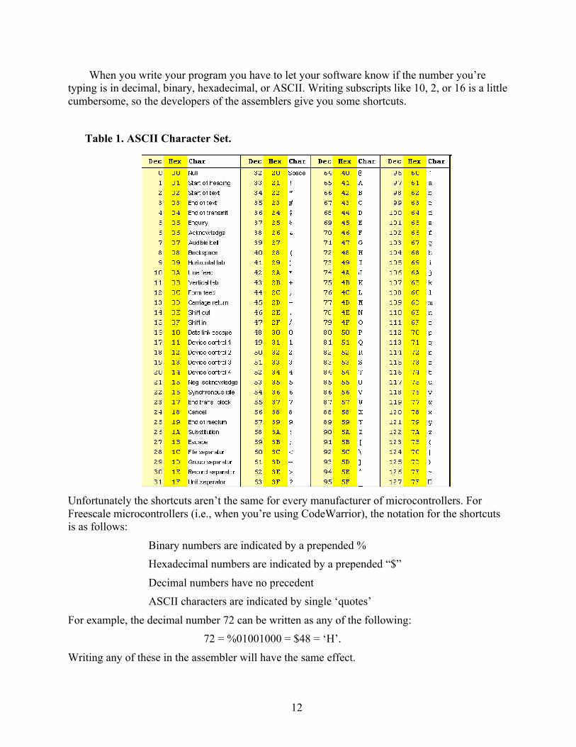
ASCII Characters The characters on your keyboard are represented by the American Standard Code for
Information Interchange, or ASCII, character set. This is a way of representing the letters, spaces, carriage returns, and numbers that you type or send across the Internet, or whatever. These have to be represented in the wires from your keyboard to your computer or in the fiber optic cables that carry your email across the country as strings of binary numbers. The way this is done is by using the ASCII character set.
Table 1 on the next page shows the characters and their corresponding decimal and hexadecimal representation. For example, when you hit the backspace key on your keyboard, it transmits the string 00001000 to your computer. In the table you will see this as decimal “8” and also as hexadecimal “8” (since 8 is the same in both decimal and hexadecimal). To transmit a capital “H,” your keyboard would send the string 00101000, which is 48 in hexadecimal.
A Word about Notation When you program your microcontroller you will be using an assembler, which is a software
package that converts the text you type into the binary strings that represent the instructions you want the microcontroller to execute. The assembler you will be using is called, CodeWarrior.
12
When you write your program you have to let your software know if the number you’re typing is in decimal, binary, hexadecimal, or ASCII. Writing subscripts like 10, 2, or 16 is a little cumbersome, so the developers of the assemblers give you some shortcuts.
Table 1. ASCII Character Set.
Unfortunately the shortcuts aren’t the same for every manufacturer of microcontrollers. For Freescale microcontrollers (i.e., when you’re using CodeWarrior), the notation for the shortcuts is as follows:
Binary numbers are indicated by a prepended % Hexadecimal numbers are indicated by a prepended “$”
Decimal numbers have no precedent ASCII characters are indicated by single ‘quotes’
For example, the decimal number 72 can be written as any of the following: 72 = %01001000 = $48 = ‘H’.
Writing any of these in the assembler will have the same effect.

13
So, why do we need so many different representations? Mostly convenience. As we mentioned, it’s hard to think in terms of long strings of 1s and 0s, so a lot of what you’ll be doing will be in hexadecimal. However, sometimes it’s useful to think in terms of binary or decimal. For example, suppose you have 8 signals from 8 fire sensors each coming from a floor of an 8-story building. Suppose, also, that the signal from each is a 1 if there’s a fire and 0 if not. Here’s the binary symbol representing the signal from the sensors when there is a fire on floor 7:
01000000. You can see that it’s a lot easier to spot which floor the fire is on when it’s written in binary; in decimal what you would see is the number 64, and in hex you would see $40. Similarly, suppose you wanted to set a counter to count from 0 to 100. It’s a lot easier to just write “100” in your code that to first figure out that it’s $64 or %1100100.
We should note that this notation is far from universal. For Intel assemblers you would indicate a hexadecimal number with postpended “H”, as in
65,535 = 0FFFFH.
You have to start the symbol with a number, otherwise Intel assemblers might think you’re just sending the ASCII character string FFFFH. In the example above, you indicate that this is not what you’re doing by adding the “0” in front.
In the same way, if you’re programming in C or C++ you indicate a hexadecimal number by prepending a “0x”, as in
0xFFFF.
A Note About Boolean Algebra
There are many instructions that perform Boolean algebra (AND, OR, XOR, NOT, etc.). Since the microcontroller mostly operates on byte-sized symbols, these instructions operate on bytes by performing the function on a bit-by-bit basis. For example, if two bytes are “ANDed” together, the first bit of the first byte and the first bit of the second byte are ANDed to give the first bit of the result. The second bit of the first byte and the second bit of the second byte are ANDed, and so on. Here’s an example: for the bytes B1 = 11001001 and B2 = 01101100,
B1•B2 = 01001000.
Instant Quiz 7. Find the Exclusive-OR of the two bytes in the example above.
Introduction to Microcontrollers Now we’re ready to start looking at actual microcontrollers, starting with what they are. A
microcontroller is a “system-on-a-chip” typically intended for embedded applications such as telephones, automobile engine control systems, remote controls, office machines, appliances, toys, etc. By “system-on-a-chip” we mean a single integrated circuit that has everything we need

14
to sense and control the outside world. Some of the things we need are on-board memory, provision for on-board clocking, lots of I/O, on-board ROM for storing programs, and so on.
In contrast, in a desktop or laptop computer many of these functions would be provided by
external integrated circuits, boards, or modules. This provides a lot of flexibility (for example, if your desktop computer doesn’t have the latest version of USB, you can add a small board to provide it) but usually at much higher cost.
Some of the characteristics of microcontrollers include
• low cost (less than a dollar to $10s) • low power (often mW)
• usually low speed (tens of MHz) • high degree of integration, and specialized functions
– lots of general-purpose onboard memory
– Analog-to-digital and digital-to-analog converters (usually more than one)
– Pulse width modulation (PWM)
– clock(s) and timer(s) – chip-to-chip communications protocols
• lots of I/O and many different types of I/O
• often emphasize interrupt latency over instruction throughput • typically programmed at a fairly low level (assembly or C/C++)
Most of these are related to the application space. Microcontrollers are intended to be used in embedded applications where quantities of thousands to millions are typical, so low cost is important. They are also often used in battery-powered applications, so low power operation is essential. Most control applications require response times in the range of a few hundred microseconds to milliseconds, so high-speed processing is usually not required. Moreover, there is a tradeoff between speed and power consumption, which is another reason you don’t often need or want high-speed devices.
Microcontrollers usually offer a high degree of integration of on-board functions. These can include, for example, a relatively large amount of general-purpose onboard memory. Microprocessors also have on-board memory, but this tends to be high-power, high speed memory that is used to store the next bunch of instructions the processor expects to execute; so it’s used to speed up the processing. The memory in a microcontroller is used to store the entire program to be run plus any needed constants or data. Also, microcontrollers typically have on-board analog-to-digital conversion circuitry, pulse width modulation (PWM) modules, clock(s) and timer(s), and support for chip-to-chip communications protocols. A high degree of integration reduces the cost but also makes the microcontroller more reliable, since there are fewer individual parts that can fail.

15
Microcontrollers typically have lots of I/O to sense, control, and communicate with the outside world. These can include simple, digital I/O pins, inputs for the analog-to-digital converters, serial pins for communications protocols, pins used for external interrupts, and many others.
We talked about interrupts a little earlier. One of the things that distinguishes microcontrollers from microprocessors is that the former emphasizes low interrupt latency, which is a measure of how quickly the microcontroller can service an interrupt.
Finally, microcontrollers are typically programmed at a fairly low level, usually using assembly or C/C++.
A typical home in the US is likely to have between one and two-dozen microcontrollers, compared to jut a few microprocessors (desktop, laptop computers, etc.). A typical mid-range car can have over 50 microcontrollers, and, as we mentioned in the Preface, the battery in your laptop has a microcontroller in it for power management.
What Goes on Inside a Microcontroller Figure 1-3 shows the typical internal structure of a generic microcontroller. Nowadays this is
called the microcontroller organization, which is a fancy word for a description of what is inside and how it’s connected. In the old days it used to be called the architecture. This term is a lot more descriptive, but it’s been appropriated by the computer scientists for something else.
Figure 1-3. The internal organization of a generic microcontroller.
The main functional elements are the Central Processing Unit (CPU), the memory, which is divided up into Read Only Memory (ROM) and Random Access Memory (RAM), and the various I/O interfaces used to connect to the outside world. These components are connected via (almost always) three data buses. The buses are sets of parallel wires, and they carry, respectively, the data to be transferred, the address that the data should come from or go to, and control lines that tell the memory or I/O interface when to transmit or receive the data.
The central processing unit fetches instructions and data, performs arithmetic or logical operations on the data, and stores the results in a special local register or general memory.

16
There are two ways in which the memory can be organized to store the instructions and data in memory—either they can be stored separately in separate parts of the memory, each with its own set of buses, or they can all be lumped together in a common memory. The latter scheme is called a “Von Neumann” architecture, named after John Von Neumann, who was a very famous scientist, mathematician, and a whole lot of other things. The former is known as a “Harvard” architecture because it was developed at Harvard. Some people like to call the Von Neumann architecture the “Princeton architecture” because Von Neumann was at Princeton and that way they could both be named after universities. Either way, as you can see, they were both named before the computer scientists lifted the name, “architecture.” Both schemes have advantages and disadvantages, but, as a practical matter, you don’t pick a microcontroller for how its memory is organized.
Figure 1-4 shows the internal components of the CPU. There are three main parts. The Arithmetic and Logic Unit (ALU) contains adders, subtractors, multipliers, dividers, and logic functions such as AND, OR, etc. Next is a set of special registers. These include one or more Accumulators, which are used to temporarily store numbers for subsequent arithmetic or logic functions, one or more Index Registers, used for something called indexed addressing (more about that later), a Program Counter (PC), which keeps track of what part of the program the CPU is going to execute next, and a memory register, which stores the number to be placed on the address bus. Finally, there is a Control Unit, comprising an Instruction Decoder and a Sequence Controller. The Instruction Decoder looks at each instruction that arrives on the data bus and figures out what to do with it (e.g., add a number to the number in an accumulator, store a number in an accumulator, or whatever). The Sequence Controller makes sure that everything runs in the proper order at the proper time (addresses put their data on the data bus, or read the data on the data bus, etc.).
Figure 1-4. The internal organization of the CPU.
Here’s how it all works together to execute a program:

17
1. The program counter places the address containing the next instruction to be executed on the address bus
2. The instruction is read from memory and decoded by the Instruction Decoder (some examples are ADD, logical AND, shift contents of a register or memory right or left, etc.—there are lots of them)
3. If data is required (for example, to be added to the number in the accumulator) the address of the data is read and the data fetched
4. The instruction is executed
5. Any results are placed in the appropriate register or memory 6. The Program Counter is advanced to the location of the next instruction
The great physicist Richard Feynman named this the “file clerk” model of computing.1 The file clerk fetches numbers on pieces of paper, does something with them, and then files the results somewhere.
As we mentioned, this is a simplified, generic model of a microcontroller. An actual device is a lot more complicated (although it does the same things). Figure 1-5 shows a real microcontroller, in fact it’s the one you’ll be using for this class, the Freescale MC9S12DG256. It’s part of the HCS12 family, so you may see it referred to in both ways. It doesn’t look very much like the generic version. Most of what you’re looking at is I/O. Starting near the middle of the left side you’ll see a box marked “PTE,” and a little below that you’ll see two boxes marked PTA and PTB. These are parallel I/O ports E, A, and B, respectively. They’re just memory addresses brought out to physical pins on the integrated circuit and they just represent digital voltage levels (5 V. for logical 1 and 0 V. for logical 0 for this device). The boxes marked DDRE, DDRA, and DDRB are control registers that you use to tell the processor whether the pins should be inputs or outputs. There are actually more of these parallel ports, such as Ports H and J. Port J has two pins reserved for external interrupts.
Now look at the upper right. There are two Analog-to-digital converters, ATD0 and ATD1. Into each there are 8 analog inputs that can be multiplexed into the converter, so you can actually have 16 analog inputs that you can digitize.
Below the ATD section you see a box marked “PPAGE.” This is the section of ROM that can be brought out externally at parallel I/O Port K.
Below this is the Timer module, attached to Port T. This module provides all kinds of useful functions related to timing and counting.
Below that are (except for a block in the middle labeled “PWM”) a bunch of modules that implement various communications protocols that can be used to connect the chip to sensors, other microcontrollers, or even computers. SCI stands for “Serial Communications Interface,” BDLC stands for “Byte Data Link Controller,” CAN (CAN bus) stands for “Controller Area Network,” IIC (aka I2C) for “Inter-Integrated Circuit,” and SPI for “Serial Peripheral Interface. They’re all just different communications protocols that people have come up with over time. The point of having so many different kinds is that it allows you to talk to a wide variety of different devices that may only have one of them.

18
The PWM (Pulse Width Modulation) module in the middle of all this provides up to 8 pulse-width modulated outputs. If you haven’t heard of this term before, it refers to the generation of square waves with an on time that you can vary, i.e., the pulse width. This is really useful for a number of applications ranging from light dimmers to controlling robot servomotors.
Figure 1-5. The HCS12 microcontroller block diagram (MC9S12DG256).2

19
What You Need to Know to Program a Microcontroller In order to program a microcontroller you need to know three things. The first is the
programming model. This is a graphical description of the special-purpose registers that we talked about earlier. The second is the memory map. This is a graphical representation of the entire memory together with a description of which addresses are RAM, which are ROM, and which addresses are set aside for special functions, such as controlling the I/O ports. The special registers in the programming model are not part of the address space. The third thing you need to know is the instruction set. This is a description of what instructions the microcontroller is designed to perform. Some examples are, “Add two numbers together,” “store a number somewhere in memory,” and “fetch a number from memory.”
In this chapter we’ll talk about the first two. The last, the instruction set, is a subject we’ll be talking about in the next chapter, and for most of the rest of this book.
The Programming Model
Figure 1-6 shows the programming model for the Freescale HCS12 microcontroller. There are two accumulators, A and B. They are each 8 bits wide. These are where the arithmetic, Boolean algebra, testing of bits to see if they’re 1 or 0, and a lot of other useful things takes place.
Next is the double accumulator, D. This isn’t an actual physical register; it’s the logical concatenation of Accumulators A and B, so it’s 16 bits long. It’s used when you’re dealing with numbers bigger than 8 bits. For example, if you’re multiplying two 8-bit numbers, the answer can be as big as 16 bits. (If you don’t believe this, try multiplying 255 x 255 and write the result as a binary number). It can also be used just to store or count big numbers.
Following Accumulator D are two 16-bit Index Registers. These are used for something called indexed addressing. (More about that in a later chapter.) They can also be used for just storing or counting big numbers.
Figure 1-6. Programming model for the HCS12.
The next register down is the Stack Pointer. This can be set to point to a region of memory that you set aside for some special purpose. For example, when you get an interrupt, you might want to save the contents of the special registers so you can use them as you service the interrupt.
20
Next is the Program Counter. This points to the address containing the next instruction to be executed. As each instruction is executed, the Program Counter figures out where the next instruction after that will be.
Finally, there is the Condition Code Register, which stores the condition code bits, V, C, N, Z, etc. that we talked about earlier.
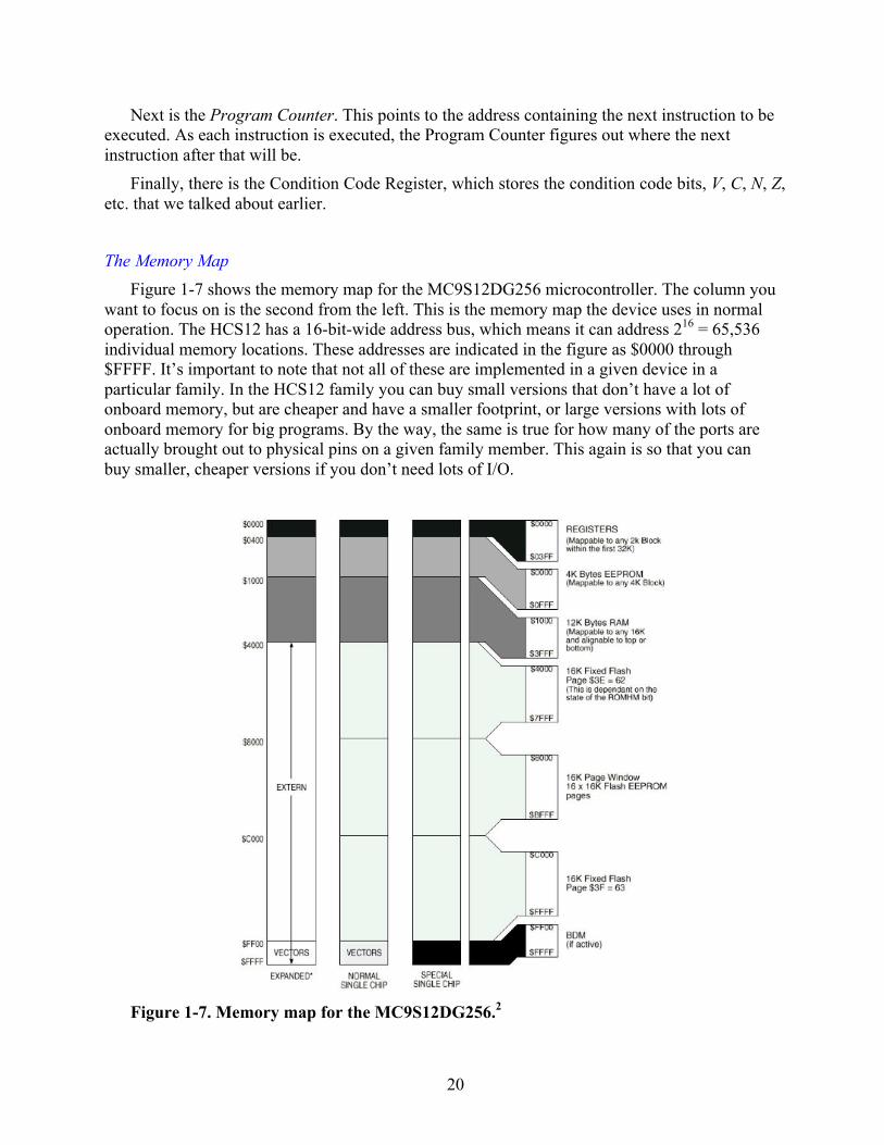
The Memory Map Figure 1-7 shows the memory map for the MC9S12DG256 microcontroller. The column you
want to focus on is the second from the left. This is the memory map the device uses in normal operation. The HCS12 has a 16-bit-wide address bus, which means it can address 216 = 65,536 individual memory locations. These addresses are indicated in the figure as $0000 through $FFFF. It’s important to note that not all of these are implemented in a given device in a particular family. In the HCS12 family you can buy small versions that don’t have a lot of onboard memory, but are cheaper and have a smaller footprint, or large versions with lots of onboard memory for big programs. By the way, the same is true for how many of the ports are actually brought out to physical pins on a given family member. This again is so that you can buy smaller, cheaper versions if you don’t need lots of I/O.
Figure 1-7. Memory map for the MC9S12DG256.2
21
There are three types of memory present in the HCS12. The first is RAM (Random Access
Memory). This type of memory can be written to or read from as the program runs, however the information in it is lost when the microcontroller is powered down. You would use this memory to store variables, such as data obtained from external sensors or results of calculations that you can afford to lose when you shut off the device. In the MC9S12DG256 version of the HCS12, the RAM is located at addresses $0000 through $03FF and $1000 through $3FFF. There are about 12,000 bytes of RAM on the chip.
The second type of memory is Flash PROM (Programmable Read Only Memory). This type of memory retains its contents when the chip is shut off. It can be erased and reprogrammed in large blocks but only when the program is downloaded; once the program is running it can’t be written to by the microcontroller. Typically the program code and any data constants are stored in ROM, so it’s available when you restart your microcontroller. The reason that you can’t write to ROM when the program is running is that you don’t want to inadvertently write some data over part of your stored program. The memory in your thumb drive is flash, which is why they’re often called “flash drives.”
The third kind of memory is EEPROM, which stands for “Electrically Erasable Programmable Read Only Memory. It’s another kind of ROM that you can use. (There’s also Flash EEPROM on the chip that you can use in the same way as the other kinds of PROM.)
You might take a minute to locate the various types of ROM in your device. Again, you just need to look at the second column from the left.
Some Popular Microcontrollers To finish up this chapter let’s look at some popular microcontrollers and microcontroller
families that you may come across. Atmel: Atmel makes a variety of different microcontrollers using several different architectures, including the AT89 (their version of the Intel 8051 described below) and the ATmega series used in the increasingly popular Arduino microcontroller boards.
Intel 8051: this is the second generation of Intel’s microcontrollers. It’s been around a long time and it dominates the microcontroller market. It’s powerful, easy to program, and uses a Modified Harvard architecture. MicroChip Technology, Inc. PIC: these are very popular among hobbyists, with over 5 billion sold. They were the first RISC (Reduced Instruction Set) microcontrollers. 8-, 16-, and 32-bit versions are available. PICs use a Harvard architecture. Motorola/Freescale: these are very popular for industrial applications. They use a Von Neumann architecture.
22
Instant Quiz Answers 1. a) 00100001
b) 11011111 2. 0 (note that the second number is just the two’s complement of the first). 3. 11110011, negative. 4. V = 0. 5. Z = N = 0. 6. FF16 = 111111112; 011111002 = 7C16. (By the way, in decimal, these numbers are 255
and 124, respectively.) 7. 𝐵1⊕ 𝐵1 = 10100101.
Homework 0. Read the article http://www.nytimes.com/2010/02/05/technology/05electronics.html 1. Convert the hexadecimal numbers on the left side of the memory map (Figure 1-7) to
decimal and binary 2. For the following two operations give the result and indicate the status of the C, V, N,
and Z bits in the Condition Code register. a) $2A
+$52
b) $AC +$8A
3. Do the following subtractions and indicate the value of the C, V, N, and Z bits
a) $7A -$5C
b) $8A
-$5C
c) $5C -$8A

23
d) $2C -$72
4. Write the sequence of hexadecimal numbers that represents the character string “HELLO
WORLD!” followed by a carriage return. 5. How many individual memory locations could you access with a 32-bit address bus?
How may with a 64-bit address bus? 6. Search the web for an MC9S08QG8 microcontroller (this is a member of the HCS08
family). Compare the programming model to that of the HCS12 you will be using in class with respect to number, sizes, and types of registers (accumulators, index registers, etc.)
7. Compare the memory map of the MC9S08QG8 with that of your HCS12.
References 1. Feynmann, Richard P., Anthony Hey, and Robin W. Allen. 2000. Feynman Lectures on
Computation. Boulder, Colorado: Westview Press. pp. 5–8. 2. “Dragon12-Plus-USB Trainer For Freescale HCS12 microcontroller family, User’s
Manual for Rev. G board Revision 1.10.” http://www.evbplus.com/download_hcs12/dragon12_plus_usb_9s12_manual.pdf. Accessed 4 April 2013.

Chapter 2. Programming the Microcontroller
In this chapter we’ll look at how you program a microcontroller. We’ll start by looking at the lowest level at which you can program, know as machine code. Machine code refers to the binary symbols that the machine interprets as instructions to be executed. Then we’ll move up to something called assembly language, which is a mnemonic representation of the machine code. This is the language we’ll be using in the rest of this book. Last, we’ll briefly look at programming in higher-level languages, such as C or C++.
Following our look at programming languages we’ll look at the programming tool that we will be using, which goes by the imposing title of the CodeWarrior Integrated Design Environment (IDE).
Programming languages At the most fundamental level, all processors are programmed in machine code, using
instructions and data represented by voltage levels corresponding to binary 1s and 0s. As an example, the machine code sequence to load Accumulator A with the number 2210 is
10000110 00010110
These two 8-bit numbers would be stored sequentially in the processor’s memory. The first number (in hexadecimal, $86) is the machine code instructing the processor to fetch the next number in memory (in this case, 000101102 = 2210) and load it into Accumulator A. To write a complete program you have to look up the machine code for each instruction you want to execute and load it into the appropriate place in memory.
This is obviously a cumbersome process. To speed the process assembly languages were developed. In assembly, mnemonics are used to represent the machine code. For example, the assembly code for the two lines above is
LDAA #22
LDAA stands for “Load Accumulator A” and the “#” sign means “the next number in memory (i.e., right after the address containing the load instruction). The “#” is used to distinguish between loading the next number and loading the number into address 22.
A piece of software known as an “Assembler” takes what you have written and converts it into the machine code above, and then loads it into the microcontroller’s memory. The CodeWarrior IDE that we mentioned above is the tool we will be using in this course.
The trend is toward programming using higher-level languages such as C or C++. This makes programming a lot easier since you’re writing straightforward programming instructions, such as
x = y + z;
25
which are pretty easy to understand. In this case, CodeWarrior will take your C or C++ code and compile it to machine code for you.
The downside is that you have very little control over how the compiler converts your program to machine code, and there is no guarantee that the resulting machine code will be the most efficient or run the fastest. This isn’t a problem unless you’re doing something that is time critical, such as developing video games. In that case, programmers often end up writing the time-critical part of the code in assembly and incorporating it into the C code as a function call.
The CodeWarrior IDE The CodeWarrior IDE was originally developed by Apple Computers for programming
Macintosh computers. It was the last in a series of earlier versions labeled, rather whimsically following a series of movie hits, Hexorcist, Lord of the Files, and Gorillas in the Disc. As you can see, this was back in the days when Apple had a sense of humor. Later it was further developed by Metrowerks and is now marketed by Freescale, a spinoff of Motorola. Special versions are available for PlayStation, Nintendo, and others.
CodeWarrior assembly code comprises four kinds of statements: 1. Instructions—these are the things the microcontroller will perform while
executing your program (e.g., LDAA). 2. Assembly Directives—these are directions to CodeWarrior that tell it how to
compile your program for subsequent download to your microcontroller. As an example, you might want to tell CodeWarrior to load your code into the microcontroller starting at address $4000.
3. Labels—these are symbols representing locations or variable names in your program.
4. Comments—these are statements that you include in your program to document what you are doing.
In writing your program, only labels may start in the first column on the page. You don’t have to start them there but if you don’t you have to write a colon after them. The columns are called a “whitespaces” and designated <ws>.
Instructions and directives must start at least one whitespace in from the margin. If you start an instruction in the first <ws> CodeWarrior will think you’re writing a label. Forgetting this is one of the most common mistakes people make when starting out.
Comments can appear anywhere but must be preceded by a semicolon. (You can actually start your comment in the first <ws> if you like, but the first character must be “;”.)
Some Useful Instructions There are a large number of instructions that you can use with the HCS12 in fact, there are
about 1,000—too many to remember unless you use them a lot. Fortunately they break down into

26
a few simple categories that are easy to remember. Here are a few that are useful for us when starting out:
• instructions that move data around • instructions that do arithmetic • instructions that perform Boolean algebra • instructions that test or manipulate data • instructions that control the flow of the program
Let’s look at some examples of each.
Instructions that Move Data Here are three instructions that move data from one place to another:
LDAA – you’ve already seen this one STAA – Store contents of Accumulator A somewhere in memory
MOVB – moves a byte from one location to another (but doesn’t change the contents of the source)
For the load and store instructions there are also versions for many of the special registers. For example, LDAB loads Accumulator B, LDD loads the double Accumulator D, LDX and LDY load Index Registers X, and Y, and there are more. Similarly, for the Store instruction, there are STAB, STX, STY, etc.
You can see how you quickly get to 1,000 instructions, but you can also see how they group together so you can more or less remember them. For example, if you were to guess that there would be an STS instruction to store the value in the Stack Pointer, you’d be correct. Another reason that there are so many instructions is that there are a lot of ways to specify what address the instruction is referring to. Remember that LDAA #22 loads the accumulator with the number 22, while LDAA 22 loads it with the number in address 22; they’re actually two different instructions.
The LDAA and STAA instructions move one byte; the equivalent loads and stores for the 16-bit index registers, Accumulator D, and the Stack Pointer move two contiguous bytes at a time. In the same way, there is a MOVW instruction that moves two contiguous bytes (a “word”) from one place to another and a MOVL that moves four contiguous bytes (a “long word”) from one place to another.
Here’s some sample code:
; remember, everything to the right of the semicolon is a comment LDAA $00 ; load A with the number in address $00 STAA $2000 ; store the contents of A in address $2000
This code moves the number in address $00 to address $2000 by first loading it into Accumulator A and then storing the contents of A in address $2000. Notice how the comments after the “;” help you to see what’s going on and, more importantly, remind you of what the code does if you come back to look at it weeks or months later.

27
You also could have done it this way MOVB $00, $2000 ; move the byte in address $00 to $2000
You might be wondering, “why do it one way rather that the other?” Well, the second way is quicker to write, but the first, it turns out, will run faster. It depends on which is more important to you at the time. Also, there are limits to how you can use an instruction. For example, you might think that there would be an instruction
MOVB A, $2000 ; move the byte in Accumulator A to $2000,
but there isn’t. What instructions are included in the instruction set is a decision made by the system architect, based on what he or she thinks is useful or can fit on the chip.
One more point, instructions are not case sensitive, so you could have written, e.g., ldaa $00. The cool kids do it this way since it’s faster to type, and I’ll start doing it most of the time from now on.
Instructions that do Arithmetic
Here are some instructions that do arithmetic. There are many more.
ADDA – Add a number to the contents of A (there’s also an ADDB, ADDD, etc.)
ABA – add contents of B to A and store the results in A
SUBA – Subtract a number from the contents of A
MUL – multiplies contents of A and B and stores the result in D (“also several divides”)
Here’s an example of something you might do with them: ldaa $00 ; load A with the number in address $00 adda $01 ; add the contents of address $01 to A staa $2000 ; store the contents of A in address $2000
What it does is to load Accumulator A with the number in address $00, then add the number in address $01 to the contents of A, then store the resulting sum in address $2000.
As we said above, there are a lot more. Some examples are Add with Carry to A (ADCA), which adds a number to the contents of Accumulator A and then adds the value of the Carry bit. You would use this to add two 16-bit (or more) numbers together. You add the two first bytes, resulting in a 1 or 0 in the Carry bit, then you “add with carry” the second two bytes, so the Carry bit from the first two bytes gets added in. There are also Add Accumulator A to Accumulator B and store the sum in A (ABA), and ABX and ABY instructions, which adds the contents of Accumulator B to the X and Y Index Registers, respectively.
Now, let’s see what you’ve learned.

28
Instant Quiz 1. How would you modify the code above so that it added the number 1 to the number in the
accumulator, rather than the number in address 1? (Hint: use a “#” sign in the adda instruction in the same way we used it in the ldaa instruction, i.e., to indicate the number rather than the address.)
2. Try to guess the mnemonic for an Add with Carry to B instruction.
Instructions that do Boolean Algebra
There are a number of instructions that perform Boolean algebra. Some examples are ANDA (AND with Accumulator A), ORAA (OR with Accumulator A), EORA (Exclusive-OR A). Naturally there are equivalent instructions for Accumulator B. These all operate only on the accumulators, so you can’t, for example, AND the contents of a memory location with a number. You can, however, complement the contents of a memory with a COM instruction. You can complement the contents of Accumulators A or B with a COMA or COMB instruction. You can also AND the contents of the Condition Code Register with an ANDCC instruction.
All of these instructions operate on a bit-by-bit basis. That is, suppose you have two bytes, ByteA and ByteB. If you AND these two bytes together, the resulting byte is calculated in this way—to get the rightmost (least significant) bit of the answer, AND the rightmost bit of ByteA with the rightmost bit of ByteB. To get the next bit to the left, AND the next bit over in Byte A with the corresponding bit of ByteB, and so on, until you’ve done all eight bytes.
There are a lot of these kinds of instructions, too. The important thing to remember is that if you want to do something that a lot of people would want to do, there’s probably an instruction for it. We’ll use them a lot in the next chapter.
Instructions that Test or Manipulate Data There are a lot of instructions that just test or manipulate data. Here are a few:
Bit test A (BITA) – this checks to see if one or more of the bits in Accumulator A are equal to 1 (you get to pick which ones to test). There’s also a BITB (of course).
Compare A (CMPA) – this compares the number in Accumulator A to any number you want. (Also, CMPB, and a lot of others.)
Bit Set (BSET) – this makes one or more bits in memory equal to 1. (Again, you get to choose which bits to make 1.)
Bit Clear (BCLR) – this makes one or more bits in memory equal to 0 (you get to pick).
Increment (INC) – this adds 1 to the contents of an address (also INCA, INCB, and INX, etc.)
Decrement (DEC) – this subtracts 1 from the content of memory (also DECA, DECB, DEX, etc.)
Logical Shift Right (LSR) – this shifts the contents of a memory address 1 bit to the right in the same way a shift register would. (There are also arithmetic shifts, which preserve the 2s complement sign of a number, and

29
rotates, which rotate the bits around, as well as all these for shifts to the left.)
A note about nomenclature: forcing a bit to be 1 is called “setting the bit,” and forcing it to be
0 is called “clearing the bit.” We’ll start using this notation from now on.
Note that BSET and BCLR only operate on memory. That is, you can’t use them to set or clear a bit in an accumulator. If you want to do this, you still can, simply by ORing the number in the accumulator with a byte that has 1s where you want to set bits, or ANDing the number with a byte that has 0s where you want to clear bits.
Instant Quiz 3. Consider the byte, 00001111. Suppose you want to set the first two bits and clear the last
two, and leave the other bits alone. Try doing this by, first, ORing the byte with 11000000 and then ANDing the result with 11111100. What do you get? Does it accomplish what you want? What happens to the bits that you don’t want to change?
Instructions that Control the Flow of the Program
Sometimes you want to alter the flow of a program, by not fetching the next instruction but instead by jumping to another part of the code. Here’s a typical example. You might be taking a series of readings from a sensor and calculating the sum. Every 10th reading you want to stop and divide by 10 to get an average. You might do this by setting a countdown counter to count down from 10 to 0 and when you hit 0, instead of taking and adding another reading you jump to another part of the code to divide by 10 and store the result. Then you want to jump back and start taking more readings.
There are two types of instructions that can do this, the branch and the jump. The branch instruction can jump ahead 127 memory locations or back -128 (it uses a 2s complement 8-bit number). A jump instruction can jump anywhere in memory. The advantage of a branch is that it only needs to fetch one byte to figure out where to branch to, so it runs a little faster. Most of the programs we’ll be writing are fairly small, so we can get away with using branch instructions.
Here are a few:
Unconditional Branch (BRA) – this branches to a label or memory location in the program
Branch if not Equal (BNE) – this branches to a label or memory location if the last instruction executed did not result in a zero (Z bit = 0).
Branch if Equal (BEQ) – branch to a label or memory location if the last instruction did result in a zero
There are a really lot of these because there are a lot of different circumstances in which it would be useful to branch somewhere if some condition is met. Some examples are Branch if Less Than, Branch if Greater Than, Branch if the C Bit is Set. The list is almost endless.

30
One more note: when we say, “the last instruction executed” we mean the last one that affected the condition codes. Not all instructions can change the CCR bits.
Addressing
Almost all HCS12 instructions operate on one or more memory locations. The address in which the data an instruction operates on is found is called the “effective address” (EA), and the way in which the effective address is specified is called the “addressing mode.” Each instruction has information in it that tells the HCS12 its addressing mode, and therefore how to figure out the effective address of the data it operates on.
To make this clearer, remember the ldaa instruction to load Accumulator A with a number. Also remember that there were two ways to say where the number to be loaded was located: the instruction ldaa #22 meant load Accumulator A with the number 22, but the instruction ldaa 22 (without the ”#” sign) meant load the accumulator with the number in address 22. These are two different addressing modes. The effective address of the first addressing mode is just the memory location right after the one in which the ldaa instruction was stored. For the second mode, the effective address is just memory location 22.
The ldaa instruction has four different addressing modes, and each has a different machine code, so essentially each is a different instruction. When you write down the 188 different types of instructions such as ldaa and add up all the addressing modes for each, you get about 1,000 possible distinct instructions; this is the scary number that we mentioned earlier.
For now, we just need to look at four fairly basic addressing modes, and they happen to be the simplest. They are
Immediate (IMM) – the number in the address immediately following the instruction is the number to be used by the instruction. Immediate addressing is indicated by a “#” sign before the number. This is the first kind of addressing you’ve seen.
Extended (EXT) – (indicated by no “#” sign) the number following the instruction is the address of the location in memory that contains the number to be used
Inherent (INH) – the affected address or register is implicit in the instruction, so no EA (example: INCA)
Extended addressing requires two bytes to specify the 16-bit address in memory so it takes
two fetches to get the full address. There is a special case of extended addressing that refers to the first 256 locations in memory. It’s called Direct Addressing (DIR). The nice thing about Direct Addressing is that it only needs 1 byte to specify the effective address, so instructions using Direct Addressing can be performed faster. Because it’s faster many of the addresses in the first 256 locations are used for possibly time-critical I/O operations.
When you begin writing your codes you don’t have to worry about the difference between extended and direct addressing because CodeWarrior automatically figures out which one you are doing. For example, if you write

31
ldaa $00FF
CodeWarrior will figure out that the effective address is in the first 255 memory locations ($FF) and it will know that it should use the Direct Addressing form of the instruction to run more efficiently. It’s as if you had written
ldaa $FF
For practice, here are some typical instructions with the addressing mode and effective address as comments:
ldab $1000 ; EXT, EA = $1000
ldaa $01 ; DIR, EA = $01
ldaa #255 ; IMM, EA = the address after the ldaa
aba ; INH, no EA
staa $2000 ; EXT, EA = $2000
movb #$20, $2000 ; IMM/EXT, EA = next address/$$2000
The movb instruction has two addressing modes and two Effective Addresses, one of each for the source and one for the target of the move.
Now you try a few.
Instant Quiz 4. Give the addressing mode and effective address for the following instructions. Also,
explain what the instruction does: a. inc $2000 b. inca c. anda $00 d. orab #%00000011
To see how you figure out the effective address in a more systematic way, consider the following code fragment:
org $4000 ; load the program starting $4000 ldaa #$22 adda $01 staa $2002 ldaa #$23 inca
The org $4000 statement is an example of an assembly directive, which we described on page 25, and will talk more about in a few pages. What it does is to tell CodeWarrior to start loading this code beginning at address $4000. Figure 2-8 shows how this program is loaded into

32
memory. The top shows a few addresses in RAM in which some data is stored ($2000, etc.). Then, beginning at address $4000 is the program above. Remember that each address only stores one byte. The first address ($4000) contains the first instruction, ldda (IMM). Of course, what actually appears there is the machine code, 10000110 ($86 in hexadecimal). Next is the number to be loaded, $22. Since the number to be loaded is I address $4001, this is the Effective Address for the load instruction.
The next instruction, in $4002, is adda (DIR). The address containing the number to be added is address $01, so $01 is the Effective address of the add instruction (not $4003). Because this is direct addressing, only one byte is needed to tell the microcontroller where the number is.
The next instruction, in $4004, is staa (EXT). The address where the contents of A will be stored is $2000, so that is the Effective Address. Note that $2000 is 16-bits long; so two bytes are needed to store the Effective Address, $4005 and $4006. Also notice that the high byte of the address, $20, is stored first, then the low byte. This scheme of high byte first goes by the charming appellation, “big-endian.” Intel processors use a “little-endian” scheme, in which the low byte goes first.
Next is an ldaa (IMM) instruction. The EA for this is $4008. Finally, there is an inca instruction, which has the same effect as adda #$01, but takes less time to run because it doesn’t have to fetch the number to add. The addressing mode of the inca instruction is Inherent (INH), so there is no Effective Address.
Figure 2-8. Memory map for the sample code shown above. The numbers in $2000–$2001 are random data.

33
Now let’s look at a piece of code that actually does something: movb #10, $1000 ; load address $1000 with 10 (decimal) ldaa #0 ; initialize A by loading it with zero loop: ; “loop” is a label adda $1000 ; add the contents of $1000 to A dec $1000 ; decrement contents of $1000 bne loop ; branch to “loop” if the dec instruction hasn’t
; decremented $1000 down to zero
The first instruction moves the decimal number 10 to address $1000. We’re going to use this as a counter to do something ten times. Next, we load A with the number 0. We have to do this because when the microcontroller first turns on there’s liable to be anything in the accumulator, and, for this example, we want to make sure we start with 0. The next statement, loop:, is a label. We know this because it’s followed by a semicolon. We could have just started it in the first <ws> to indicate that it’s a label, but since you can’t see where the first <ws> is on the page we’ll guarantee that it’s interpreted as a label using the semicolon.
Let’s skip the next two instructions for now and look at the bne instruction. This says, “branch to where the label ‘loop’ is if the previous instruction didn’t result in a 0. That previous instruction is the dec $1000 instruction; it subtracts 1 from the contents of address $1000, which was originally loaded with the number 10. After it executes the dec instruction, the number in $1000 is 9. Since this isn’t 0, the program branches to the loop label. It then runs through the instructions again and decrements $1000 again, resulting in the number 8 being in $1000. Since this isn’t 0 it branches again, and again, … until it decrements $1000 from 1 down to 0. Now the bne instruction sees that the last operation did result in a 0, so it doesn’t branch to loop. Instead, it just goes on to the next instruction in memory, whatever that is.
What the program is doing is just looping around ten times, but each time it goes through a loop it adds the number in $1000 to the number in the accumulator. For the first loop it adds 10, the next time around it adds 9, then 8, 7,…1. It just adds the numbers from 1 to 10 to get 55, but it does this by adding in the reverse order. This may seem like a rather mundane thing to do, but it’s the heart of a lot of useful activities. For example, you might want to take 10 readings from a sensor and add them all together. Now you see why we had to initialize the accumulator by loading it with 0. This is such an important task that it gets its own instruction, Clear A (CLRA). (Of course there’s a Clear B, Clear Interrupt Mask, Clear V Bit, and lots more.)
A few notes about the program:
1. Nothing has to be justified, the rules are that labels must either start in the first column or be followed by a colon and instructions must have at least one space (<ws>) preceding them.
2. You can have blank spaces between lines to make it more readable. 3. The instructions and comments are not case sensitive, although the labels are. 4. It’s usually better to count down to zero that to count up to a number, because the CCR
keeps track of zeros for you and there are lots of branch instructions that use the Z bit.
34
Before moving on, there’s a handy convention for describing the instructions in your programs. Here are the rules:
A register name (e.g., “A” for Accumulator A) indicates both the register itself and its contents
An arrow (→) indicates a transfer (…) indicates the contents of a memory location
((…)) indicates and address whose contents are the actual address of the data (this is used in something called Indirect Addressing, which you don’t need to think about this for now)
Here are some examples:
$100 → A (load A with the number $100)
($1000) → A (load A with the number in address $1000)
B → ($2000) (store contents of Accumulator B in address $2000)
A + ($2000) → A (add the number in $2000 to contents of A)
A + B → A (adds contents of Accumulators A and B and stores the result in A)
($2000) → ($2010) (move contents of address $2000 to address $2010, but don’t delete contents of $2000)
Instant Quiz
5. For the example code above, replace the comments using this convention. Note that you can’t represent the loop label with the convention since it’s not an operation. Also, don’t worry about the bne instruction.
We should note that Intel uses the revers convention. For example, adding the contents of address $01 to Accumulator A would look like this
A ← A + (01).
Because of the popularity of Intel devices some microcontroller texts based on Freescale or other vendors may use this notation, so you may come across it sometime.
Some Useful Assembler Directives There are a large number of useful assembly directives. You’ve already seen one—org,
which tells CodeWarrior where in the microcontroller’s memory to place the next bit of code.
Here’s another useful one, Equate (EQU or equ, directives are not case sensitive). Equate associates a symbol with a value. The label can only be defined once in the program, so you can’t change it later. Here’s an example of how you might use it:

35
ROMStart: equ $4000 org ROMStart ldaa #$22 staa $200
This tells CodeWarrior that every time you write ROMStart, it should replace it with the number $4000 when converting your program to machine code.
Here’s another example: roomTemp: equ 20 ; roomTemp = 20 C ldaa #roomTemp ldab roomTemp
The equ directive says to CodeWarrior, “every time I write roomTemp, you use the number 20 (typical room temperature in Celcius). The second line loads Accumulator A with the number 20, and the third line loads Accumulator B with the number in address 20.
The big advantage in using this is that it makes the program self-documenting. What we mean by this is that if you’re looking at some long code and there are a bunch of “20’s” in it, you don’t know their significance. If you write the code as above, wherever you write roomTemp you will know at some later time that you were talking about normal room temperature, and every time you write “20” you’re not, you’re just writing the number “20.”
Putting all this together, your code might look like this:
ROMStart: equ $4000 counter: equ $1000 ; “counter” = $1000 org ROMStart movb #10, counter ; load address $1000 with 10 ldaa #0 loop: ; “loop” is a label adda counter ; adds contents of $1000 to A dec counter ; decrement $1000 bne loop
Notice that we used the label counter in three places, the movb, adda, and dec instructions.
In each it will be replaced with the number $1000 by CodeWarrior.
We should note two more points. The first is that when you open up CodeWarrior for the first time you will notice that it already adds the first and third lines to the code for you, as a convenience. If, for some reason, you wanted to start your code at, e.g., $5000, you would need to add a separate org directive.

36
The second point is about the bne instruction. Branches use something called Relative Addressing (REL). You don’t need to do anything about this since CodeWarrior does it for you. You do have to think about the Effective Address, though. Actually there are two EAs, one for when it takes the branch and one for when it doesn’t. If the microcontroller takes the branch in the example above it jumps to the adda counter instruction (the label doesn’t appear anywhere in the memory; it’s just used by CodeWarrior to figure out where to jump to (i.e., the Effective Address). For this example, the EA is the address containing the adda instruction. If it doesn’t take the branch the EA is just the next address after the one containing the bne instruction.
Now it’s your turn:
Instant Quiz 6. Rewrite the code above to use Accumulator B as the counter. (Hint: you will need an aba
instruction.) 7. For the code you write in question 5, show how it is loaded into memory (like the one in
Figure 2-8). Indicate the addressing type and Effective Address (if any) for each instruction.
Instant Quiz Answers 1. ldaa $00 ; load A with the number in address $00
adda #$01 ; note the “#” sign staa $2000 ; store the contents of A in address $2000
2. ADCB 3. After the OR you get 11001111; after the AND you get 11001100. Yep. Nothing. 4. a) EXT, EA = $2000, adds 1 to the number in $2000
b) INH, no EA, adds 1 to the number in Accumulator A c) DIR, EA = $00, ANDs the number in Accumulator A with the number in address $00 d) IMM, EA = address right after the instruction, ORs the number in Accumulator B with
the number %00000011
5. movb #10, $1000 ; 10 → ($1000)
ldaa #0 ; 0 → A loop: ; “loop” is a label
adda $1000 ; ($1000) + A → A
dec $1000 ; A – 1 → A bne loop ; branch to “loop” if the dec instruction hasn’t
; decremented $1000 down to zero

37
6. Changes are shown in blue:
ROMStart: equ $4000 ; you don’t need this line counter: equ $1000 ; “counter” = $1000 org ROMStart ldab #10 ; load Accumulator B with 10 ldaa #0 loop: ; “loop” is a label aba ; adds contents of B to A decb ; decrement B bne loop
7. Here’s the solution for the version above:
Address
Instruction EA
$4000 ldab
(IMM) $4,001
$4001 10 ($0A)
$4002 ldaa
(IMM) $4,003
$4003 0
$4004 aba
(INH) N/A
$4005 decb
(INH) N/A
$4006 bne (rel) $400
4 or
$4007 … $4007

38
Homework 0. Read Understanding the Microprocessor Part 1 at
http://arstechnica.com/paedia/c/cpu/part-1/cpu1-1.html (follow the links at the bottom of each page for the entire article).
1. The HCS12 microcontroller instruction set evolved from the original Motorola 6800 microprocessor. This device reputedly had a number of undocumented instructions, the most important of which was the HCF instruction. Search the web and briefly report what this instruction does.
2. Write a code fragment that adds the even numbers from 0 to 10 and stores the result in
memory address $2000. 3. Modify your code from problem 1 to increment Index Register X each time a number is
added. (You have to take some care to do everything in the right order or the branch instruction won’t work.)
4. Write a code fragment to load the numbers in addresses $2001 through $2004
successively into Accumulator A. Each time you load a number, increment the contents of Index Register X if the number was zero. (Note that when you do a load, the Z-bit is set or cleared depending on whether the number loaded is 0 or not.)
5. For the following code, explain which statements are instructions, which are assembly
directives, which are labels, and which are comments:
; this program adds 3 to address $2000 and increments Accumulator B org $4000 ldaa $2000 adda #3 ; add 3 to (A) staa $2000 incb ; increment B 6. For each instruction in problem 5, indicate the addressing mode and effective address, if
any.

Chapter 3. I/O Ports
In this chapter we’ll focus on the parallel I/O ports available in the HCS12. These ports support digital connections at the individually programmable bit level. We’ll see how to read from or write to those bits, but first, we’ll begin by looking at a few more instructions, in particular, those that test or manipulate data. These are particularly useful in detecting and controlling the bits of the parallel I/O ports.
Instructions that Test Data Suppose you want to test if one particular bit in an accumulator is a “1” (e.g., bit 2 in
Accumulator A). For example, suppose the bits in the accumulator represents the state of eight different fire alarms on eight floors of a building. You would like to know which floor the fire is on so you don’t have to turn on all the sprinklers on all the floors, just the one with the fire.
How would you test, for example, if there were a fire on the second floor (we’re going to number our floors starting with 0 so that the bit numbers line up)? It’s simple, Just AND the number in the accumulator with the number %00000100:
ANDA #%00000100
The result in the accumulator will be %00000100 if there was a 1 in bit 2 of the number originally in A, but it will be %00000000 if the number originally in bit 2 was a 0. In the first case the Z bit will be 0 (cleared); in the second the Z bit will be 1 (set). You just have to look at the Z bit to see if the fire is on the second floor.
The only problem with this is that now if you want to test to see if the fire is on, e.g., the third floor, you’ve destroyed the information in A. You would have had to store it somewhere and then reload the accumulator to do this next test.
As an aside, if you wanted to test if the fire is on either the second or the fourth floor (or both), you can test both floors at the same time with the instruction
ANDA #%00010100
Now the Z bit will be 1 only if both bits 2 and 4 are 0, if either one or both are 1 the Z bit will be cleared. If the Z bit is 0 you have a fire on one or the other of these floors, or both, but you still have the problem that the information in A has been destroyed, so you can’t easily test other floors.
Instant Quiz 3. How would you test if there is a fire on any of the floors?
The solution to the destruction of the data is to use a Bit Test instruction, BITA (or BITB for Accumulator B). Here’s the syntax

40
BITA #%00010100
Now, the Z bit will be set or cleared as if you had done an ANDA, but the data is left unchanged.
The number used for the test is called a “mask.” You can also use a mask stored somewhere in memory if you like, as in
BITA $2000
which uses the number in address $2000 as the mask (you’re using Extended addressing if you do).
One thing to keep in mind is that you can’t do bit tests on numbers in memory, just the accumulators.
Instructions that Manipulate Data Now, suppose you want to change one (or a few) bits in a memory location. For example,
suppose you want to force bit 2 of address $0000 to be “1”. Just load the contents of the address into an accumulator and OR it with the right mask:
LDAA $00 ORA #%00000100 STAA $00
Take a second and convince yourself that this forces the digit in bit 2 to be a 1, no matter what it was to begin with.
The problem now is that this takes three instructions and a bunch of memory to do. To shorten this process, use the “BSET” instruction:
BSET $00, %00000100
This has the same effect as ORing the bit with 1, but with just one instruction, and you don’t have to use the accumulator, so it’s much more efficient.
Note the syntax, BSET address, mask. You list the target address first, then the mask with the bits to be set, separated by a comma. A few remaining points:
1. You can set any number of bits you want with a single instruction, for example
BSET $1000, %01010101
2. You can only use BSET with a memory address; you can’t use it with an accumulator, so it’s the opposite of a BITA instruction
3. You can’t use a number in memory as a mask, as you do with a BSET instruction; you can only an Immediate mask. That is, the instruction above is equivalent to
BSET $1000, #%01010101
In fact, you can write it either way and CodeWarrior will understand it.

41
To clear a bit in memory, just use a BCLR instruction, for example
BLCR $2000, %00100011
This forces bits 0, 1, and 5in address $2000 to be 0, and leaves the other bits as they were. It’s important to remember that with either a BSET or BCLR, anywhere there is a 0 in the
mask the corresponding bit in the address is left alone!
Instant Quiz 2. In address $1000, how would you force bits 0, 1, and 3 to be 1 and bit 6 and 7 to be 0,
leaving the other bits as they were? 3. What do the following instructions do?
a) bset $20FA, %00010010
b) bclr 2, $03
c) BLCR $2000, %00000000
Parallel I/O Ports You may recall from Chapter 1 the large number of parallel I/O ports available in the HCS12.
As a reminder, since this is an ebook and we don’t have to worry about wasting paper, on the next page is Figure 1-5 from that chapter, again. For now, we’re concerned with the parallel ports. In the figure, these are Ports A, B, and E (labeled PTA, PTB, and PTE), but there are actually a lot more of these, such as Ports J and H. Also, many of the other ports can be configured to act as parallel I/O ports if you need more. As we mentioned in Chapter 1, not all of these are brought out in every member of the HCS12 family for reasons of size and cost.
To see how these ports work, let’s look at Port A, shown functionally in Figure 3-2. The figure shows a corner of the microcontroller integrated circuit and we’re pretending that that’s where Port A resides (physically it could be anywhere the chip designer wants). Port A is connected to memory address $0000, and the bits in this address are brought out physically to pins external to the chip, so they are accessible to the outside world. A logical 1 in any bit position in this address appears on the outside as a voltage level, for this chip as a 5 V signal. A logical 0 appears as a 0 V signal (i.e., ground).
So far, we haven’t said yet whether a given pin is an input or an output. Actually, you control which one it is by writing a control byte to the box marked “DDR,” which stands for Data Direction Register. In this case we have DDRA, which is the Data Direction Register for Port A. Any place you write a 1 in the DDR, the corresponding bit in Port A is an output. The value of the output bit (0 or 1, corresponding to 0V or 5V), is determined by the value of the corresponding bit in address $0000. Now you can use this bit to, for example, turn on a sprinkler system on the floor where the fire is.
Similarly, a 0 in a bit position in DDRA means that the corresponding bit in Port A is an input. The value of the bit (0 or 1) will be determined by whatever is connected to the physical pin—a fire sensor, for example. In the figure on the next page, bits 7, 2, and 0 are outputs and the rest are inputs. For the bits that are outputs, the corresponding external voltages are 0, 5, and 5V.

42
Figure 3-1. The HCS12 functional blocks.
Figure 3-2. Functional representation of Port A. (DDR stands for "Data Direction
Register.”)
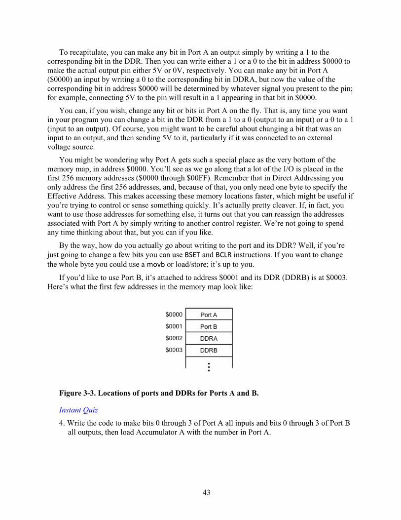
43
To recapitulate, you can make any bit in Port A an output simply by writing a 1 to the corresponding bit in the DDR. Then you can write either a 1 or a 0 to the bit in address $0000 to make the actual output pin either 5V or 0V, respectively. You can make any bit in Port A ($0000) an input by writing a 0 to the corresponding bit in DDRA, but now the value of the corresponding bit in address $0000 will be determined by whatever signal you present to the pin; for example, connecting 5V to the pin will result in a 1 appearing in that bit in $0000.
You can, if you wish, change any bit or bits in Port A on the fly. That is, any time you want in your program you can change a bit in the DDR from a 1 to a 0 (output to an input) or a 0 to a 1 (input to an output). Of course, you might want to be careful about changing a bit that was an input to an output, and then sending 5V to it, particularly if it was connected to an external voltage source.
You might be wondering why Port A gets such a special place as the very bottom of the memory map, in address $0000. You’ll see as we go along that a lot of the I/O is placed in the first 256 memory addresses ($0000 through $00FF). Remember that in Direct Addressing you only address the first 256 addresses, and, because of that, you only need one byte to specify the Effective Address. This makes accessing these memory locations faster, which might be useful if you’re trying to control or sense something quickly. It’s actually pretty cleaver. If, in fact, you want to use those addresses for something else, it turns out that you can reassign the addresses associated with Port A by simply writing to another control register. We’re not going to spend any time thinking about that, but you can if you like.
By the way, how do you actually go about writing to the port and its DDR? Well, if you’re just going to change a few bits you can use BSET and BCLR instructions. If you want to change the whole byte you could use a movb or load/store; it’s up to you.
If you’d like to use Port B, it’s attached to address $0001 and its DDR (DDRB) is at $0003. Here’s what the first few addresses in the memory map look like:
Figure 3-3. Locations of ports and DDRs for Ports A and B.
Instant Quiz
4. Write the code to make bits 0 through 3 of Port A all inputs and bits 0 through 3 of Port B all outputs, then load Accumulator A with the number in Port A.

44
An Example: Process Control Automation Let’s look at a simple example of how you might use all of this to automate a process control
sstem. Suppose you have an assembly line with four inputs, I0, I1, I2, and I3, and four outputs, O0, O1, O2, and O3. The inputs can be anything—switches, sensors, or whatever. Similarly, the outputs can be motors, warning lights, solenoid-controlled valves, or whatever. Now suppose that the outputs are controlled by the inputs as follows:
• Output 0 turns on whenever input 2 is on AND either input 1 OR input 3 is on • Output 1 turns on whenever input 1 is on AND input 2 is off • Output 2 turns on whenever input 1 is on OR inputs 2 AND 3 are both on • Output 3 turns on whenever input 0 is on
The Boolean expressions for these conditions are as follows:
𝑂0 = 𝐼1+ 𝐼3 ∙ 𝐼2, (1)
𝑂1 = 𝐼1 ∙ 𝐼2, (2)
𝑂2 = 𝐼1+ 𝐼2 ∙ 𝐼3 , (2)
𝑂3 = 𝐼0. (4)
If you are familiar with Programmable Logic Controllers (PLCs), which are devices used for industrial automation, the program to do this (called ladder logic) is shown in Figure 3-4. If you’re not familiar with these devices, no matter—the important thing to know is that they’re expensive.
Figure 3-4. PLC ladder logic for the industrial control problem.
The question we would like to address is, how do we do this with a 50¢ microcontroller? You start by connecting the inputs and outputs to pins on the parallel ports. Suppose you make Port A all input bits and Port B all outputs. Then connect the inputs from your industrial system (i.e., I0

45
through I3) to bits 0 through 3 of Port A, and the outputs (O0 through O3) to bits 0 through 3 of Port B. Now we have to write a program to sense the bits at Port A, figure out what the bits of Port B should be, and then write those bits to the port.
Let’s start with one of the outputs, O1 (bit 1 of Port B, which we’ll start calling B1). Equation (2) tells us that B1 will be 0 if either A1 is 0 OR A2 is 1. (Take a second and convince yourself that this is correct.) Here’s the prescription for figuring out B1:
1. Set up your DDRs (forgetting to do this is a major failure mode for beginners) 2. Initialize B1, usually by making it 0 (you usually don’t want it turned on when you first
start up your program since it might turn whatever it controls on, possibly with unpleasant consequences)
3. Load Accumulator A from Port A 4. Test bit A1; if it’s 0 then B1 should be 0, so clear the bit and go back to step 3; if it’s 1,
go on to test A2 I Step 5 5. Test bit A2; if it’s 1, make B1 0 and go back to step; if it’s 0, make B1 =1 (since you
know that A1 is already 1 or you wouldn’t have gotten to this step) 6. Go to step 3 and stat the whole process again so that you are continually sampling the
inputs and updating the outputs If you like flowcharts, here’s the one for this process:
Figure 3-5. Flow chart for bit B1.

46
Instant Quiz
5. Develop a flowchart for the problem 𝐵1 = 𝐴1 ∙ 𝐴2. If you prefer, just write out the prescription, as we did above.
Now, just take each piece of the flow chart and convert it to assembly code. Here’s what you get:
bclr $02, %00001111 ; set up DDRs for Ports A, B bset $03, %00001111 bclr 1, %00000010 ; Initialize Bit 1 loop: ldaa $0 ; load Port A into Accumulator A bita #%00000010 ; Test if A1=1, if it isn’t, branch
beq clearB1 ; to clearB1. If it’s 1, continue to next test bita #%00000100 ; Test if A2= 0, if it isn’t, bne clearB1 ; branch to clearB1. If it is 0, proceed to set B1. bset 1, %00000010 ; then go back to “loop” to bra loop ; start again clearB1: bclr 1, %00000010 ; Clear Bit 1, then bra loop ; branch to "loop" to start again
Let’s go through it a step at a time. The first three lines set up the DDRs for Ports A and B and clear bit B1. Next, the loop label is where we want to branch to each time after we figure out what B1 should be, so that we are constantly looking to see if the inputs change, and updating the outputs when they do.
Inside the loop is where we do all the testing. First, we load the accumulator with the number in Port A (address $0000). Then, we bit test bit A1. If it’s equal to 0 we branch to the label clearB1, which clears the bit and then branches to loop to continue testing. If A1 equals 1, then we have the possibility that B1 should be 1, but only if bit A2 is equal to 0. So, we test A2 and branch to clearB1 if it is not equal to 0. If it is equal to 0 then we have arrived at a point where both A1 is 1 AND A2 is 0. This means that B1 should be 1. We set B1 and then branch to loop, skipping the last lines that clear the bit.
There are lots of different ways to do this, and this is a source of confusion for beginners. You may be thinking to yourself, “how did he know to start by testing if A1 is equal to 1 rather than testing if A1 was equal to 0? Well, you can do that if you like, but you just have to switch the positions of the “No” and “Yes” answers, and then you have to switch the beq and the bne. It’s a little like doing a double negative. This is one of the reasons why there are so many possibilities. The thing to do as a beginner is to just dive in, write some code, then test your code

47
with some possible combinations of A1 and A2. If it works with all possible variations of A1 and A2, you’re good. If not, just back out a little to see where it went wrong. If you practice enough you will get some confidence that you can get to the right answer.
Once you get good at it the trick is to find the way that is efficient enough to satisfy your application requirements (fast enough, smallest memory usage, or whatever) while not taking forever to figure it out.
Some (possibly) Helpful Hints Before leaving this topic, here are some helpful hints that can speed up your programming by
helping you test several bits at a time in some circumstances. Feel free to ignore them if they seem overly complicated. You can always do things in a “brute force” way by testing each bit one at a time.
The first is to use ORs or NORs as much as possible. Here’s an example of why this is so:
Suppose you want to do B1 = A1 + A2 + A3 (essentially this is a 3-input OR gate). You could do this by the following prescription
1. Read Port A by loading the result into Accumulator A 2. Test A1. If it’s 1, make B1 = 1 and go to step 1 to see if the number at Port A has changed
3. If A1 ≠ 1, test A2. If A2 = 1, make B1 = 1 and go to step 1 again 4. If A2 ≠ 1, test A3. If A3 = 1, make B1 = 1. If A3 ≠ 1, the number at Port A has failed all
three tests, so Make B1 = 0. Then go back to step 1 to continue the process. You can see that testing the number (A3, A2, A1) one bit at a time can be a long process,
both in coding time and in execution time when the program in running in the microcontroller. Here’s an easier way:
loop: ldaa 0 bita #%00001110 beq clearB1 bset $1, %00000010 bra loop clearB1: blcr $1, %00000010 bra loop
What is happening is that the bit test at line 2 tests all three bits at once. If the result is zero, it means that none of the three bits was a 1, so branch to clearB1 to clear the bit. If one or more of the bits were 1, the result of the bit test would be 1, so the beq test fails and the next instruction executed is the bset, followed by the branch to loop.
Notice that we put the label clearB1 on the same line as the bclr instruction. You can do it either way, but doing it this way cleans up your code a bit. It doesn’t affect how CodeWarrior converts the assembly code into machine code. We did the same thing with the loop label and the ldaa instruction.
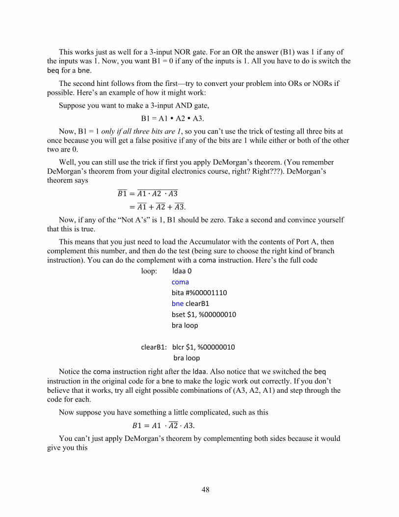
48
This works just as well for a 3-input NOR gate. For an OR the answer (B1) was 1 if any of the inputs was 1. Now, you want B1 = 0 if any of the inputs is 1. All you have to do is switch the beq for a bne.
The second hint follows from the first—try to convert your problem into ORs or NORs if possible. Here’s an example of how it might work:
Suppose you want to make a 3-input AND gate,
B1 = A1 A2 A3. Now, B1 = 1 only if all three bits are 1, so you can’t use the trick of testing all three bits at
once because you will get a false positive if any of the bits are 1 while either or both of the other two are 0.
Well, you can still use the trick if first you apply DeMorgan’s theorem. (You remember DeMorgan’s theorem from your digital electronics course, right? Right???). DeMorgan’s theorem says
𝐵1 = 𝐴1 ∙ 𝐴2 ∙ 𝐴3
= 𝐴1+ 𝐴2+ 𝐴3. Now, if any of the “Not A’s” is 1, B1 should be zero. Take a second and convince yourself
that this is true. This means that you just need to load the Accumulator with the contents of Port A, then
complement this number, and then do the test (being sure to choose the right kind of branch instruction). You can do the complement with a coma instruction. Here’s the full code
loop: ldaa 0 coma bita #%00001110 bne clearB1 bset $1, %00000010 bra loop clearB1: blcr $1, %00000010
bra loop
Notice the coma instruction right after the ldaa. Also notice that we switched the beq instruction in the original code for a bne to make the logic work out correctly. If you don’t believe that it works, try all eight possible combinations of (A3, A2, A1) and step through the code for each.
Now suppose you have something a little complicated, such as this
𝐵1 = 𝐴1 ⋅ 𝐴2 ⋅ 𝐴3. You can’t just apply DeMorgan’s theorem by complementing both sides because it would
give you this
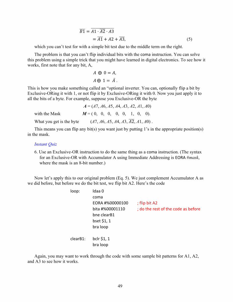
49
𝐵1 = 𝐴1 ⋅ 𝐴2 ⋅ 𝐴3
= 𝐴1+ 𝐴2+ 𝐴3, (5) which you can’t test for with a simple bit test due to the middle term on the right.
The problem is that you can’t flip individual bits with the coma instruction. You can solve this problem using a simple trick that you might have learned in digital electronics. To see how it works, first note that for any bit, A,
𝐴 0 = 𝐴,
𝐴 1 = 𝐴 .
This is how you make something called an “optional inverter. You can, optionally flip a bit by Exclusive-ORing it with 1, or not flip it by Exclusive-ORing it with 0. Now you just apply it to all the bits of a byte. For example, suppose you Exclusive-OR the byte
A = (A7, A6, A5, A4, A3, A2, A1, A0) with the Mask M = ( 0, 0, 0, 0, 0, 1, 0, 0).
What you get is the byte (A7, A6, A5, A4, A3, 𝐴2, A1, A0) . This means you can flip any bit(s) you want just by putting 1’s in the appropriate position(s)
in the mask.
Instant Quiz
6. Use an Exclusive-OR instruction to do the same thing as a coma instruction. (The syntax for an Exclusive-OR with Accumulator A using Immediate Addressing is EORA #mask, where the mask is an 8-bit number.)
Now let’s apply this to our original problem (Eq. 5). We just complement Accumulator A as we did before, but before we do the bit test, we flip bit A2. Here’s the code
loop: ldaa 0 coma EORA #%00000100 ; flip bit A2 bita #%00001110 ; do the rest of the code as before bne clearB1
bset $1, 1 bra loop clearB1: bclr $1, 1 bra loop
Again, you may want to work through the code with some sample bit patterns for A1, A2, and A3 to see how it works.

50
Instant Quiz Answers 1. ANDA #%11111111 ;(the Z bit will be set if all the floors are fire-‐free.) 2. BSET $1000, %00001011 BCLR $1000, %1100000 3. a) Sets bits 1 and 4 of the contents of address $20FA, leaves remaining bits unchanged
b) Clears bits 0 and 1 of address 2. (Remember that $03 = %00000011.) c) Nothing! The instruction clears bits where there is a 1, but the mask is all 0s.
4. bclr $02, #00001111 bset $03, #00001111 ldaa $00 5.
6. eora #%11111111 ; (or you could just use eora #$FF or eora #255).
51
Homework 0. Go to http://www.freescale.com/webapp/sps/site/prod_summary.jsp?code=CW-
HCS12X&fpsp=1&tab=Design_Tools_Tab and download the “Special” version of CodeWarrior HCS12(X). It’s free. Load it onto an available PC and try running some of the code from the first laboratory exercise on it.
Also, go to http://www.freescale.com/files/microcontrollers/doc/ref_manual/CPU12RM.pdf and download the HCS12 Reference Manual. It’s 414 pages long. Do not be afraid.
1. Write a code fragment to make the even-numbered bits of Port A all inputs and the odd-
numbered bits all outputs. 2. Make a three-input AND gate: Write the code to make PORT A bits 0–2 all inputs and
PORT B bit 1 an output, then add the code to set PORT B bit 1 if bits 0 AND 1 AND 2 of PORT A are all set, and clear the bit otherwise. Don’t forget to include the appropriate ORG statement, and loop your code so that it repeatedly tests the inputs.
3. Repeat problem 2 for a 3-input NOR gate. 4. Write the code to realize an Exclusive-OR gate (recall that 𝐴⊕ 𝐵 = 𝐴𝐵 + 𝐴𝐵). (Hint:
start by writing the flow chart.) N.B. If you would like to test your codes with your newly installed CodeWarrior, Use some
memory location (e.g., $1000) as your input instead of Port A. Then start by moving 0 to $1000 and put your code in a continuous loop that increments $1000 starting from 0.

Chapter 4. Indexed Addressing
So far everything we’ve done has used one of four modes of addressing—Inherent (INH), Immediate (IMM), Extended (EXT), or Direct (DIR). There are several other types of addressing modes, the most important of which is Indexed Addressing (designated IDX). In this chapter we’ll see how to use Indexed Addressing and what it’s good for.
Indexed Addressing Indexed Addressing uses the contents of the X or Y Index Registers as a base, to which an
offset is added to get the effective address. (Indexed Addressing can also use the Stack Pointer or Program Counter, but for now we just need X and Y.)
There are three types of Indexed Addressing that we need to know about: – Constant offset indexed addressing
– Auto pre/post decrement/increment indexed addressing – Accumulator offset indexed addressing
Constant Offset Indexed Addressing
In Constant Offset Indexed Addressing a constant is added to the number in the base (the X or Y registers) to get the EA. The number in the base is not changed; it’s just used for the calculation of the EA.
The syntax is
instruction offset, base register
Here’s an example of how you would use it
ldaa 3, X
Suppose the current number in the X Register is $2000. The effect of this instruction is to load Accumulator A with the contents of address $2003 (the offset, 3, plus the contents of the X Register). After the instruction is executed, the number in X is still $2000. (You’ll see in a bit that with some indexed addressing modes the content of the base changes.)
Actually there are three different kinds of Constant Offset Indexed Addressing, characterized by how many bits are needed to specify the value of the offset, which can be 5, 9, or 16 bits. One of the reasons for having three different kinds is efficiency. If you just need a 5-bit offset you don’t need to fetch two bytes to execute the instruction. You do need two bytes for a 16-bit offset. The offset is a 2’s complement signed number. For example, with a 5-bit signed number you can represent an offset ranging from -16 to +15.
The size of the offset only affects the size and execution time of the code, so you don’t have to worry about it for now. We’ll revisit the issue of execution time later.

53
So (you are probably asking), what good is it? Well, suppose you’ve just taken some data from a sensor and the data resides in addresses $2001 through $2100. Now you would like to add all these numbers (for example, to take an average). The only way to do this with the tools you have so far, is to just do brute force addition:
clra ; clear A so you don’t add whatever is there to the sum adda $2001 adda $2002 adda $2003 ⋅ ⋅ ⋅ adda $2100
This can make for a lot of typing and it uses up a lot of memory. With Constant Offset Indexed Addressing you can do it this way
clra ; clear A ldx #$100 ; $F -‐> X continue: adda $2000, X dex ; decrement X bne continue ; continue adding until (X) = 0
The first two lines initialize A and loads the X Register with $100. The rest is a loop, between the label continue and the bne instruction. This loop does three things: first, it adds the contents of the address $2000 + X to whatever is in A. Next, it decrements X. Finally, it tests to see if the decrement resulted in a 0, and branches to continue if it didn’t.
Let’s go through a few cycles of this loop:
The first time around the number in X is $100, so the adda instruction adds the contents of address $2000 + $100 = $2100 to A, then it decrements X, so that now the number in X is $00FF (remember, we’re subtracting in hexadecimal). Then it tests to see if $00FF is zero, which it isn’t, so the program branches to continue, and does the next loop.
The second time around the number in X is $0FF, so the adda instruction adds the contents of address $2000 + $0FF = $20FF to A, then it decrements X, so that now the number in X is $0FE. Then it tests to see if $0FE is zero, which it isn’t, so the program branches to continue, and does the next loop.
The third time around the number in X is $00FE, so the adda instruction adds the contents of address $2000 + $00FE = $20FE to A, then it decrements X, so that now the number in X is $0FD. Then it tests to see if $00FF is zero, which it isn’t, so the program branches to continue, and does the next loop.
54
The program will continue until the X register contains the number $001, and the number in $2001 has just been added. Now when it does the dex, the number in X is 0, so the program doesn’t take the branch to continue; instead it continues on with the next instruction.
Instant Quiz 4. Suppose Port A is connected to a sensor that produces a constant stream of 8-bit numbers
that represent the analog signal it is sensing. Write a program that takes $100 readings from Port A and stores them in addresses $2001 through $2100. You can store the numbers in any order you like, that is, you don’t have to put the first one in $2001, the second in $2002, etc. That is, you could, if you wish, put the first number in $2100, the second in $20FF, and so on.
Auto Pre/Post Decrement/Increment Indexed Addressing
In the example above, it would be useful and faster if the dex instruction were done automatically. This is the motivation behind the next addressing mode, which goes by the odd-sounding title, “Auto Pre/Post Decrement/Increment Indexed Addressing.”
The reason it sounds odd is that it’s really four versions of the same idea. The four are
Auto Pre-decrement Indexed Addressing Auto Pre-increment Indexed Addressing
Auto Post-increment Indexed Addressing Auto Post-decrement Indexed Addressing
The way it works is that the offset is added (increment) or subtracted (decrement) to or from the contents of the base register (e.g., X) but now the contents of the base register are changed. You indicate an increment by putting a “+” sign next to the base register and a decrement by putting a “-” sign next to the base register.
The pre- or post- refers to whether the Effective Address is calculated before or after the instruction is executed. If you want to increment or decrement the base register before the instruction is executed you put the + or – sign to the left side of the base register (e.g., +X). If you want to do it after the instruction is executed you put the +/- sign on the right side (e.g., X+).
Here are some examples (suppose before each instruction is executed, the contents of X and Y are $2000 and $2100, respectively):
ldaa $1E, +X ; $2000+$1E = $201E → X; ($201E) → A
staa $1, -‐Y ; $2100-‐1 → Y; A → ($20FF)
dec 3, X+ ; ($2000) -‐1 → ($2000); $2000+3 = $2003 → X
adda 1, Y-‐ ; ($2100) + A → A; $20FF → Y
The first is an example of auto pre-increment. The number $1E is added to the number in X and the sum ($201E) stored in X. This number is the Effective Address for the load instruction.

55
In the second, the number 1 is subtracted from the number in Y and the result is both the new number in Y and the address where the contents of A are stored.
In the next two instructions, the offset is added to or subtracted from the base register after the instruction is executed. In the first of these the effective address is $2000, since the increment isn’t performed until after the dec instruction is executed. That means the number in address $2000 is decremented by 1, then the offset, 3, is added to X. In the last instruction, the number in $2100 is added to A and then 1 is subtracted from the number in Y.
Instant Quiz 2. For each of the examples below, find the addressing mode, the Effective Address, and the
content of the X Register when the instruction is completed. Assume the number in the X Register is $3000 before the instruction is executed.
a) ldaa 3, X+
b) staa 3, -‐X
c) adda 5, X+
d) inc 5, X-‐
Now we’re going to do an example of how you might use this kind of addressing. It uses a
new instruction that you haven’t seen, cpx. What this does is to compare the number in the X Register with a mask by calculating the difference. If they’re the same it sets the Z bit because the difference is zero. If not, it clears it. Note that it doesn’t change the number in X. We’re using it here to count up to a number rather than counting down to zero.
Here’s the code:
ldx #$2001 ldy #$2101 continue: ldaa 1, X+ suba #20 staa 1,Y+ cpx #$2101 ; this instruction compares (X) with
; the mask $2100 and adjusts the Z-‐bit ; accordingly
bne continue
What does it do? The first two instructions load $2001 and $2101 into X and Y, respectively. They will be our counters. Here’s what happens in the first few cycles of the loop:

56
1st time around
The numbers in X and Y are still $2001 and $2101, respectively. The ldaa instruction loads A with the number in address $2001, and then adds 1 to the number in X, giving $2002. The next instruction subtracts 20 from the number in A. The next stores the result in $2101 and adds 1 to the number in Y. Next, the compare instruction compares (Immediate) the number in X ($2102) with the mask, $2101. Since the difference is not zero, it branches to the label, continue.
2nd time around
The ldaa instruction loads A with the number in address $2002, and then adds 1 to the number in X, giving $2003. The next instruction subtracts 20 from the number in A. The next stores the result in $2102 and adds 1 to the number in Y (now $2103). Next, the compare instruction compares (Immediate) the number in X ($2103) with the mask, $2101. Since the difference is not zero, it branches to the label, continue.
This continues until the number in X is $2101. Now the cpx instruction returns a difference of zero, so the program doesn’t take the branch. What has happened is that all the numbers in addresses $2001 through $2100 have had the number 20 subtracted from them and the results stored in $2101through $2200.
Why do something like this? Well, suppose you’re taking readings of temperature in a room and normal room temperature is 20C. What this code does is to calculate and store the difference between each reading and room temperature. Suppose you want to take an average of 100 readings. If you start adding 100 numbers each of which is typically within a few degrees of 20, you’ll get a result around 2000. This is too big to manipulate in an 8-bit accumulator so you end up doing a lot of extra coding to get 16-bit accuracy. If, on the other hand, you take an average of the differences from room temperature you’ll probably get a number pretty close to zero, so you can do the arithmetic in an 8-bit accumulator, and your life is a lot easier. If you need the actual average, just add 20 to the result.
Accumulator Offset Indexed Addressing
The last kind of indexed addressing that we are going to look at is called Accumulator Offset Indexed Addressing because it uses the contents of one of the accumulators as the offset. Either Accumulators A or B can be used, and also the double accumulator, D, can be used for large offsets. The offset is treated as an unsigned number, i.e., as a positive number between 0 and 255 for Accumulators A or B, and 0 to 65,535 for Accumulator D.
The syntax is simple:
ldaa B, X This loads Accumulator A with the contents of the address pointed to by the sum of the
numbers in B and X. The contents of B and X are unchanged. You can use this to do some very elegant things. An example is something called a “lookup
table.” Suppose you need to sample the data from a sensor attached to Port A and take the square root. We’re going to take the integer square root, which means that we are going to represent the square root as an integer rather than a decimal number. For example, suppose we want the square

57
root of 2. We can’t save it as 1.4 because we can’t store decimal fractions, only integers. To get around this we’ll store it as the integer 14.
Calculating square roots is a pretty complicated thing to do in a microcontroller, or even a microprocessor with floating point arithmetic for that matter. A much easier way to do it is to use a lookup table, which stores the answer for the range of numbers we’re interested in.
For simplicity, suppose the sensor just sends 4 bits, so that we need a table with 16 possible entries. Here’s the table we need to store
What you see are the 16 possible 4-bit numbers we can get from the sensor. The middle
column is the decimal square root of each, and the right column is the integer representation of each.
Now let’s set up the lookup table in memory with a bunch of movb instructions. (We’ll see in the next chapter a much easier way to do this.)
movb #00, $2000 movb #10, $2001 movb #14, $2002 movb #17, $2003 : movb #39, $200f
and now add the code to use Accumulator Offset Indexed Addressing to pick the number in memory ($2000, etc.) that corresponds to the square root of the number at Port A:
ldx #$2000 ldab $00 ; load B from Port A ldaa B, X ; load A from address (B+A)

58
The ldx instruction makes the base equal to $2000. The next instruction loads Accumulator B with the number at Port A (address $00). Finally, the last instruction loads A with the number in the address pointed to by the sum of the numbers in B and X.
Here’s how it works. Suppose the number at Port A is 3. This is loaded into B in the second instruction. The third instruction loads A with the number in address 3 + $2000 = $2003. This is the number 17, the integer square root of 3.
Instant Quiz
3. Find the effective address of the ldaa instruction in the following code:
ldab #$A ldy # $5000 ldaa B, Y
A Last Note
Finally, you can do some pretty sophisticated stuff, like this
movb 3, X-‐, 5, Y
CodeWarrior will figure out from the locations of the commas and the minus sign the unique addresses of the source and target for the move instruction. In this example, ‘3, X-‐‘ can only indicate Auto Post-decrement Indexed Addressing for the source. The Effective Address for the source is the number in X, and 3 will be subtracted from the number in X as the instruction is completed. For the target of the move, ‘5, Y’ can only indicate Constant Offset Indexed Addressing; the address of the target of the move is 5 plus the number in Y, and Y doesn’t change. You would characterize the addressing mode of this instruction as Auto Post-decrement IDX/Constant Offset IDX.
This can clean up your code a bit. Suppose you want to take a succession of readings from Port A and store each result sequentially, starting at $2100. Here’s how you might do it:
movb #0, $2000 ; set up lookup table movb #10, $2001 movb #14, $2002 movb #17, $2003 : movb #39, $200f ldx #$2000 ldy $2100
loop: ldab $00 movb B, X, 1, Y+ bra loop

59
The addressing mode of the movb instruction is Accumulator Offset/Auto Post-increment. It takes the number in the memory location whose address is the number in B plus the number in X (the number in this address is the integer square root of the number at Port A that was loaded into B, and moves it to the memory location whose address is the number in Y. Then it increments Y by 1 to get ready for the next square root value.
The unconditional branch at the end means that the process will just loop until all your memory is full, so you might want to set up a counter with a bne instruction to limit the number of times it does this.
Instant Quiz Answers 1. movb $0, $2 ; you remembered to set up DDRA, of course
ldx #$100 ; $F -‐> X
continue: ldaa $00 ; load A from Port A staa $2000, X ; store the number that was in Port A in ($2000+X) dex ; decrement X bne continue ; continue load/store until (X) = 0 2. a) Auto post-increment, $3000, $2003
b) Auto pre-decrement, $2FFD, $2FFD c) Auto post-increment, $3000, $3005
d) Auto post-decrement, $3000, $3005 3. $5000A
Homework 0. Read Chapter 3, Sections 3.1-3.7 and 3.9-3.10 of the CPU12 Reference Manual that you
downloaded previously. 1. For the following code, indicate the addressing mode, the effective address for each
instruction, and the value in the Index Register, X, after the instruction is completed: org $4000 ldab #3 ldx #$2015 ; load X immediate with $2015 staa 2, X staa 6, -‐X staa 2, X+ staa B, X

60
2. Using whatever form of indexed addressing you like, write the code to load the numbers
1 through $F into the addresses $2001 through $200F, respectively. 3. Write a code fragment to do the following: suppose the number at Port A is N. Load the
number in Port A into Accumulator A, then increment the number in address N + $1000. For example, if the number is 4, increment the number in address $1004. Repeat 100 times.

Chapter 5. Assembly Directives
In this chapter we are going to look at some very useful assembly directives. Remember that assembly directives are instructions you give to CodeWarrior to tell it how to implement your program; they are not instructions that the microcontroller executes during runtime. In fact, they’re not executed at all. Instead, they are evaluated by CodeWarrior during compilation. You’ve already seen a few of these, such as the org statement, which tells CodeWarrior where in the microcontroller’s memory to put the code that follows it.
Before we start investigating assembly directives, we’re going to take a little time out to look in some detail at the HCS12 Reference Manual that you’ve downloaded previously. In the last chapter you used this to better understand the various addressing modes. The manual also tells us a lot of other interesting things, including everything you want to know about every instruction the microcontroller can execute, how long it takes, what addressing modes are supported by the instruction, how the instruction affects the Condition Code bits, and lots more.
The HCS12 Reference Manual The HCS12 Reference Manual contains all the logical information you need for basic
programming of the device. It doesn’t contain physical information, such as how the ports are mapped or how you control the various I/O modules. That’s in a different reference manual that we’ll see later.
Figure 5-1 shows the first page of the Table of Contents. A lot of this should seem familiar to you. In Chapter 2 of the reference manual you’ll find the programming model and its special registers. In Chapter 3 you’ll find the description of the addressing modes that you were assigned to read in the last chapter. Chapter 4 describes how instruction queues are used to speed up operation (not that interesting for us at this point).
Chapter 5 is the beginning of the heart of the manual for our purposes. It describes the instructions in the instruction set grouped according to functionality, much as we did when we first began talking about the instruction set. Here you will see topics such as, “Load and Store Instructions” or “Addition and Subtraction Instructions.” In this chapter these are described at a fairly high level, usually with a table showing all the members of the group. For example, Figure 5-2 shows the table for the Addition and Subtraction instructions just mentioned. You’ll also see some odd-looking groups such as “Fuzzy Logic Instructions.” “Fuzzy Logic” refers to a kind of logic in which the variables can have values not just of 1s or 0s, but several or many values in between. It’s more representative of how our brains work and is useful in fields such as artificial intelligence. (And you were beginning to think that the HCS12 was just good for turning on light bulbs.) Actually there’s a whole chapter on fuzzy logic (Chapter 9). It covers such interesting topics as “Defuzzification,” covered in Section 9.2.3.
Chapter 6 is the “Instruction Glossary.” This contains every single instruction that the microcontroller can execute, together with the machine code for each, the exact steps the microcontroller must go through to execute the instruction, and how the instruction can affect the CCR bits.

62
Figure 5-1. Table of Contents (page 1) of the HCS12 Reference Manual.

63
Figure 5-2. Table of Addition and Subtraction instructions.
In Chapter 6 each instruction gets its own page, so this section is quite long. In fact, the entire reference manual is 414 pages long, and Chapter 6 takes up more than half of them. This is ok since you don’t actually read it. Mostly you just look through it to find the instruction you want.
Figure 5-3 shows the page for the LDAA instruction. At the top, in large bold letters, you see the mnemonic, LDAA, twice (in case you missed the first one). In between is the title of the instruction, “Load Accumulator A.” Next is a description of what it does,
Loads the content of memory location M into accumulator A. The condition codes are set according to the data.
Next, you’ll see, “CCR Details.” This shows how the 8 bits in the Condition Code Register are affected by the instruction. The meaning of the symbols is given in Section 6.3, at the beginning of Chapter 6, reproduced in Figure 5-4. For example, the “Δ” symbols under the N and Z bits means that those bits can change, depending on the number that is loaded into A. The V bit is cleared, and the other bits are unaffected by the instruction. If you are as lazy as I am you don’t actually need to flip over to Section 6.3 since the descriptions of how the bits are affected are listed right below the box.
In the box below the CCR Details you get a large amount of useful (and perhaps some not so useful) information. In the first column, marked ‘Fource Form,’ you are looking at the syntax for each addressing mode of the instruction. For example, the first form, LDAA #oper8i, represents Immediate addressing (note the “#” sign). You find out what oper8i means in Section 6.5 Source Forms. A partial list of the various forms is reproduced in Figure 5-5. To see how this works, look at the third entry from the bottom
LDAA oprx16, xysp

64
From Figure 5-5 we see that oprx16 is “Any label or expression that evaluates to a 16-bit value.” Also, xysp means any of the 16-bit registers, X, Y, S (Stack Pointer), or the Program Counter.
Figure 5-3. The LDAA page from the HCS12 Reference Manual.
Figure 5-4. Section 6.3 of the Reference Manual showing the symbols indicating effects
of instructions on the CCR bits.
The addressing mode of this instruction is just Constant Offset, using oprx16 as a 16-bit offset and the number in the X, Y, SP, or PC register as the base. Since the offset is 16 bits, the addressing mode is IDX2. If you couldn’t figure this out, the next column, “Address Mode,” tells you what the addressing mode is. You may sometimes need to look at this a little carefully to see what addressing modes are available. Fore example, a movb instruction does not have a Direct (DIR) addressing mode. It does have an Extended mode, but it’s a little less efficient due to the extra address byte fetch.
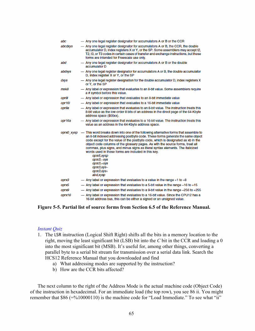
65
Figure 5-5. Partial list of source forms from Section 6.5 of the Reference Manual.
Instant Quiz 1. The LSR instruction (Logical Shift Right) shifts all the bits in a memory location to the
right, moving the least significant bit (LSB) bit into the C bit in the CCR and loading a 0 into the most significant bit (MSB). It’s useful for, among other things, converting a parallel byte to a serial bit stream for transmission over a serial data link. Search the HCS12 Reference Manual that you downloaded and find
a) What addressing modes are supported by the instruction? b) How are the CCR bits affected?
The next column to the right of the Address Mode is the actual machine code (Object Code) of the instruction in hexadecimal. For an immediate load (the top row), you see 86 ii. You might remember that $86 (=%10000110) is the machine code for “Load Immediate.” To see what “ii”

66
means, you look in another section in Section 6. In Section 6.4 Object Code Notation, you will find a listing (reproduced in Figure 5-6) of all the possible symbols you can have for the argument of the instruction. In the figure you will see that “ii” means “8-bit immediate data value.” This is just the 8-bit number to be loaded into A. If, instead of Immediate Addressing, you were doing extended, you would have
B6 hh ll
in which B6 is the machine code for “Load Extended,” hh is the high byte of the 16-bit address containing the number to be loaded into A, and ll is the low byte. (The last symbol is two lower case “els”, not two upper case i’s.)
Figure 5-6. Object code notation.
The last column in Figure 5-3 is the “Access Detail.” This is a listing of all the steps the microcontroller has to take to execute the instruction. There are two columns, one for our HCS12 and one for the older version, the MC68HC12. Obviously you want the HCS12. The access details are represented by a bunch of letters, given in another listing in Section 6.6 Cycle-by-Cycle Execution. It’s a long list so we’ve only shown a few of them in Figure 5-7. For a “Load Immediate” Figure 5-3 shows a single “P,” which, from Figure 5-7, means “Program word fetch. For a “Load Extended” we see “rPf,” which means three steps in the execution.
You can look up what these mean in the figure, but for us it turns out that the important thing is not the actual steps the microcontroller takes; it’s how many steps it takes. Each step (each letter in the table) takes exactly one bus clock cycle, so you can use this to figure out how long the instruction takes to execute. By adding up the total number of letters in your entire code (including any branches), you can figure out how long your code takes to run. For example,

67
ldaa #$3 takes one bus cycle (P), whereas ldaa $3000 takes three (rPf). If you bus is running at 1 MHz the first will take 1 µs; the second will take 3 µs.
Figure 5-7. Partial listing of access detail symbols.
This is a very useful thing to know, but even more useful is that you can also figure out how you can change your code to make it run faster. This is really useful if your code isn’t running fast enough and you really don’t want to pay for a faster device.
To see a simple example of how this works, take the Instant Quiz.
Instant Quiz 2. The two code fragments below do the same thing. For each, find how many clock
cycles it takes and how long each takes if the bus clock is running at 2 MHz. Which fragment runs faster?
; Fragment 1 ldaa #$FF staa $03
;Fragment 2 movb #$FF, $03
Shift Operations In Instant Quiz Question 1 we saw an example of a shift operation. There are actually 21
different kinds of shift operations, summarized in Figure 5-8, which is taken from Table 5-12 of the Reference Manual. These 21 operations break down into three categories—Logical Shifts, Arithmetic Shifts, and Rotations. Each of these breaks down into two types—shifts to the left and shifts to the right. Finally, each type can be applied to a number in a memory location or one
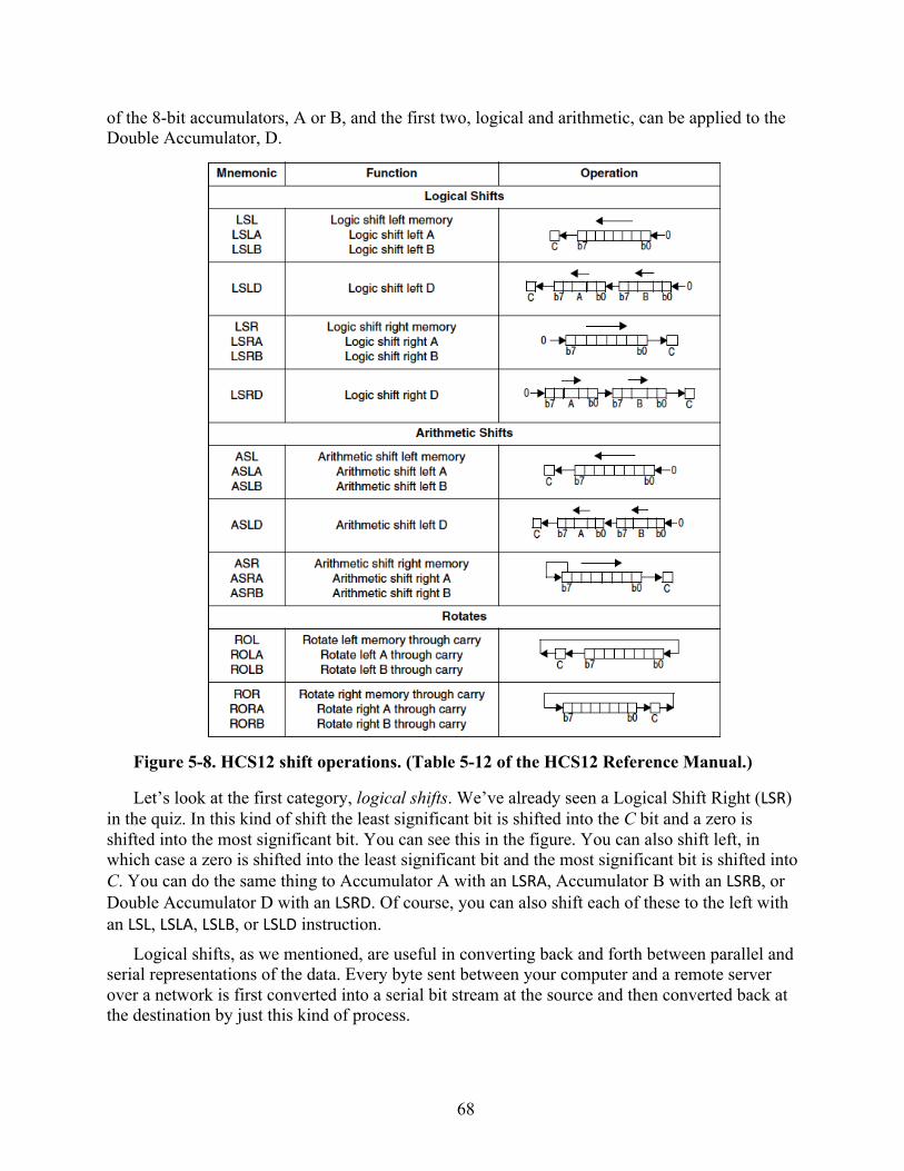
68
of the 8-bit accumulators, A or B, and the first two, logical and arithmetic, can be applied to the Double Accumulator, D.
Figure 5-8. HCS12 shift operations. (Table 5-12 of the HCS12 Reference Manual.)
Let’s look at the first category, logical shifts. We’ve already seen a Logical Shift Right (LSR) in the quiz. In this kind of shift the least significant bit is shifted into the C bit and a zero is shifted into the most significant bit. You can see this in the figure. You can also shift left, in which case a zero is shifted into the least significant bit and the most significant bit is shifted into C. You can do the same thing to Accumulator A with an LSRA, Accumulator B with an LSRB, or Double Accumulator D with an LSRD. Of course, you can also shift each of these to the left with an LSL, LSLA, LSLB, or LSLD instruction.
Logical shifts, as we mentioned, are useful in converting back and forth between parallel and serial representations of the data. Every byte sent between your computer and a remote server over a network is first converted into a serial bit stream at the source and then converted back at the destination by just this kind of process.
69
The next category is that of the arithmetic shifts. These, too, can shift left or right, and can shift the contents of a memory or an accumulator. Arithmetic shifts to the left look exactly like logical shifts left. This might strike you as an odd thing to do, but what is odder is what happens in arithmetic shifts to the right. For these shifts, the least significant bit is again shifted into the C bit, but the most significant bit is shifted back into itself.
To see why they do such a strange thing, let’s apply a logical shift right to the number %00000110 (= 610). The result is %0000011 (= 310). Shifting to the right is equivalent to dividing by 2. Shifting to the right twice is equivalent to dividing by 4, and so on. Similarly, shifting to the left is equivalent to multiplying by 2.
Here’s where the problem occurs: suppose the number to be shifted is %10001100 (= -11610). When you do a logical shift right, you get %01000110 (= +70!!!). What has happened is that the 1 in the most significant bit has been shifted to the right, turning a 2’s complement negative number into a positive number.
To get around this problem, the Arithmetic Shift Right instruction shifts the low 7 bits to the right, shifting the lowest bit into the C bit, but then it shifts what was the most significant bit back into itself, preserving the original sign of the number, as shown in the figure. For the example above (%10001100 = -11610), after the shift we get
%11000110 = -5810,
which is correct. We should note three things about arithmetic shifts. First, when using shifts to the right as
division by 2, you get a rounding error whenever the least significant bit is a 1. For example, shifting %00000011 (= 310) to the right once gives %00000001 (= 1, not 1.5). Second, arithmetic shifts to the left do not preserve the sign of the answer, so you can’t use it to multiply negative numbers by 2, 4, etc. Third, you can arithmetically shift the Double register D left, but not right.
Instant Quiz 3. a) For the binary number %11001000, find the result of two successive arithmetic shifts
to the right. Is the answer equal to the original number divided by 4? b) For the same number, find the result of two arithmetic shifts to the left.
The final kind of shift in this group is the rotate. From Figure 5-8 you can see that you can
rotate the number in a memory location or Accumulators A and B, and you can rotate right or left. If you are rotating the number right, the least significant bit (b0 in the figure) is shifted into the C bit, bits b7 through b1 are shifted right one position, and the number that was in the C bit before the shift is shifted into the b7 position. If you executed, for example, a rora nine times, the number in Accumulator A would just be the one you started with.
Rotate left works the same way, except the most significant bit is shifted into the C bit and the value that was in the C bit is shifted into the least significant bit of the memory or accumulator.

70
You can do some pretty neat things with the rotation instructions. One of them is shown in Figure 5-9. This device is known as a “Linear Feedback Shift Register” (LFSR). It’s also known as a pseudo-random pattern generator, for reasons that will soon be obvious.
Figure 5-9. A Linear Feedback Shift Register (LFSR).
To implement this in a microcontroller, you would use a rotate right instruction (A, B, or a memory address, whatever works for you), but before you executed the instruction, you would first figure out the Exclusive-OR or bits B3 and B0 and put the result in the C bit (remember that you did an Exclusive-OR for homework in Chapter 3). Then execute the rotate.
What this device does is to generate a pseudo-random stream of bits. “Pseudo-random” means that it looks random but will eventually start to repeat itself. The number of bits generated before the pattern repeats is determined by how large the shift register is and which bits you use for the inputs of the Exclusive-OR. The device in Figure 5-9 will generate 255 bits before repeating.
To get it started you have to initialize it by loading it with a “seed” number. Any number that isn’t zero will do. Then you start it running and watch the pseudo-random sequence come out.
Instant Quiz 4. Suppose the seed number in the LFSR is %11001011. What will be the numbers in the
shift register after the first shift? After the second and third? After each shift, what will be the value of the C bit in the CCR?
It turns out that this is a very useful thing to do. In fact, you do it all the time without
knowing it. Every time you get a web page from a server that isn’t very close to you (like on the same campus) your request and the information returned from the server is scrambled using this technique. The reason for scrambling the data is that the clocks in your computer and the computer at the other end don’t run at exactly the same rate. At the receiving end of any transmission the receiver circuitry is trying to sample each incoming bit at just the right time to tell if it’s a 1 or a 0. If it’s clock is running at a slightly different rate eventually it will eventually miss a bit or sample the same bit twice. The way the receiver gets around this is to use the transitions in the incoming data (i.e., from 1 to 0 or 0 to 1) to re-sync its own clock to that of the sending circuit.
The problem is, what happens when you send a very large number of 1s in a row (or 0s in a row)? The receiver has no transitions to sync up to and you will start getting errors eventually. The solution is to run your data through a LFSR. This will start generating transitions quickly as the Exclusive-OR sees a string of 1s (or 0s) in a row. This technique is used in a communications

71
protocol named SONET (for Synchronous Optical Network) and almost all of your long-distance communications use this protocol.
Some Useful Assembly Directives We learned in Chapter 2 that assembly (or assembler) directives are instructions to the
assembler to do specific actions. You’ve already used an important example of an assembly directive, the org statement; which told CodeWarrior where to start putting your compiled code. Remember that assembly expressions are evaluated during compilation, not at runtime, and the resulting machine code is what is loaded onto the microcontroller. In this section we’re going to look at some really useful assembly directives. In the next section we’ll look at a related topic, assembly expressions.
We’ll start with a few of the simplest directives:
EQU: The Equate (EQU) directive assigns a value to a label. Whenever that label appears in your code, CodeWarrior replaces it with the value. Here’s an example of the syntax
roomTemp: EQU 20 : ldaa #roomTemp ; this instruction loads A with the value 20
Wherever you write roomTemp CodeWarrior replaces it with the value 20. The EQU directive can appear anywhere but the value cannot be changed later in the program with another EQU statement (i.e., it’s global). The equ directive isn’t case sensitive, but, as always, the label you use is.
SET: SET also assigns a value to a label in the same way as an equ, but the value can be changed anywhere in your code.
INCLUDE: The Include directive includes text from another file. An example is
INCLUDE mc9s12dg256.inc
This directive adds the contents of file mc9s12dg256.inc to your code as if you had typed it in yourself. You will find some version of this in your CodeWarrior stationery. It does some useful things such as equating easily remembered mnemonics with numbers. An example is equating the label DDRA with the number $02. We’ll see how this works in a while.
SECTION: This directive establishes a relocatable section of code. This is useful if you have several people working on separate parts of a big project that you want to integrate into a single program.

72
Equate directives are particularly useful for self-documenting your program so that you can remember what you did when you look at it months or years later. For example, in the equ example above, you can see that you are loading the normal room temperature, 20 C, into A. If you just wrote ldaa #20 you might miss the significance of the instruction.
To see how this can really help, let’s recall the code that we wrote in Chapter 3 to implement 𝐵1 = 𝐴1 ∙ 𝐴2:
org $4000 movb #$ff, 3 ; set up DDRs for Ports A, B
movb #0, 2 loop: ldaa 0 ; load Port A into Accum A bita #%00000010 ; Test if A1=0, if it is, beq clearB1 ; branch to clearB1. If ; it’s 1, continue to next test bita #%00000100 ; Test if A2=1, if it is, bne clearB1 ; branch to to clearB1. If it’s ; it’s 0, proceed to set B1. bset 1, %00000010 ; then go back to “loop” to bra loop ; to start again clearB1: bclr 1, %00000010 ; Clear Bit 1, then bra loop ; branch to "loop" to start again
Remember that this code looks at A1 and clears B1 if it’s 0, but if it’s not, it goes on to look
at A2. If A2 = 0, then it sets B1, otherwise B1 is cleared. You don’t really see what it’s doing unless you read it carefully and recognize a bunch of things such as that address 0 is Port A and address 0 is DDRA, and so on.
Now, let’s add a few equate directives at the beginning of the code:
A1: equ %00000010 A2: equ %00000100 BIT1: equ %00000010 PORTA: equ $00 PORTB: equ $01 DDRA: equ $02 DDRB: equ $03 ROMStart: equ $4000
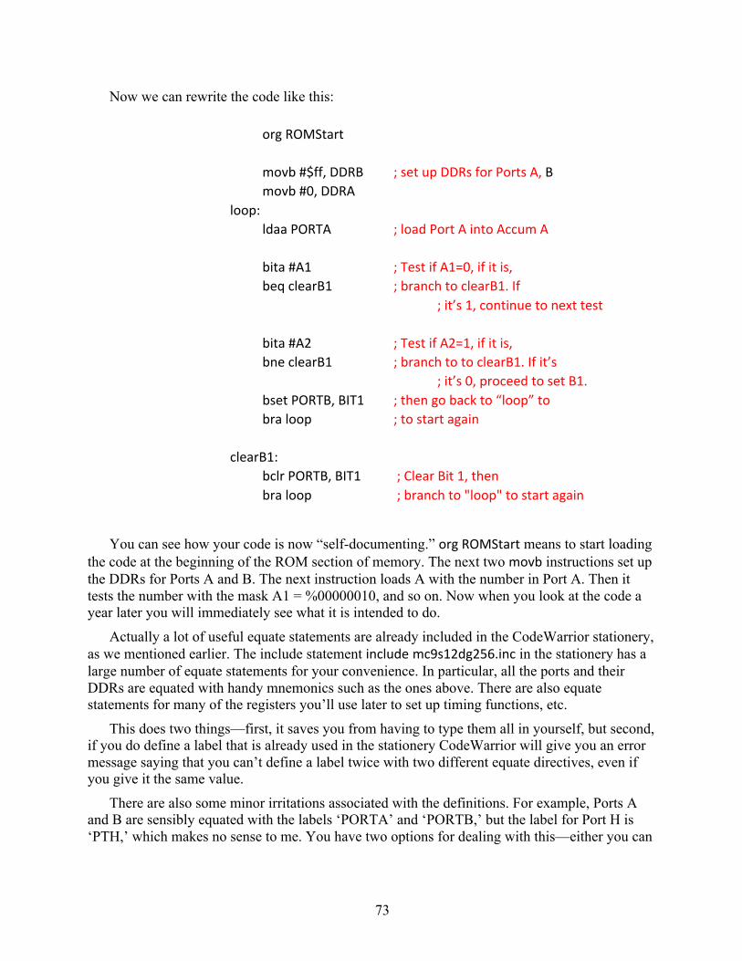
73
Now we can rewrite the code like this: org ROMStart movb #$ff, DDRB ; set up DDRs for Ports A, B
movb #0, DDRA loop: ldaa PORTA ; load Port A into Accum A bita #A1 ; Test if A1=0, if it is, beq clearB1 ; branch to clearB1. If ; it’s 1, continue to next test bita #A2 ; Test if A2=1, if it is, bne clearB1 ; branch to to clearB1. If it’s ; it’s 0, proceed to set B1. bset PORTB, BIT1 ; then go back to “loop” to bra loop ; to start again clearB1: bclr PORTB, BIT1 ; Clear Bit 1, then bra loop ; branch to "loop" to start again
You can see how your code is now “self-documenting.” org ROMStart means to start loading the code at the beginning of the ROM section of memory. The next two movb instructions set up the DDRs for Ports A and B. The next instruction loads A with the number in Port A. Then it tests the number with the mask A1 = %00000010, and so on. Now when you look at the code a year later you will immediately see what it is intended to do.
Actually a lot of useful equate statements are already included in the CodeWarrior stationery, as we mentioned earlier. The include statement include mc9s12dg256.inc in the stationery has a large number of equate statements for your convenience. In particular, all the ports and their DDRs are equated with handy mnemonics such as the ones above. There are also equate statements for many of the registers you’ll use later to set up timing functions, etc.
This does two things—first, it saves you from having to type them all in yourself, but second, if you do define a label that is already used in the stationery CodeWarrior will give you an error message saying that you can’t define a label twice with two different equate directives, even if you give it the same value.
There are also some minor irritations associated with the definitions. For example, Ports A and B are sensibly equated with the labels ‘PORTA’ and ‘PORTB,’ but the label for Port H is ‘PTH,’ which makes no sense to me. You have two options for dealing with this—either you can
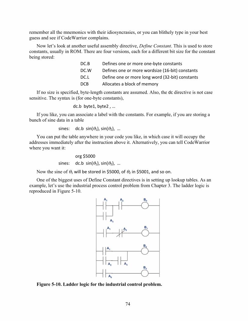
74
remember all the mnemonics with their idiosyncrasies, or you can blithely type in your best guess and see if CodeWarrior complains.
Now let’s look at another useful assembly directive, Define Constant. This is used to store constants, usually in ROM. There are four versions, each for a different bit size for the constant being stored:
DC.B Defines one or more one-‐byte constants DC.W Defines one or more wordsize (16-‐bit) constants DC.L Define one or more long word (32-‐bit) constants DCB Allocates a block of memory
If no size is specified, byte-length constants are assumed. Also, the dc directive is not case sensitive. The syntax is (for one-byte constants),
dc.b byte1, byte2 , …
If you like, you can associate a label with the constants. For example, if you are storing a bunch of sine data in a table
sines: dc.b sin(θ1), sin(θ2), …
You can put the table anywhere in your code you like, in which case it will occupy the addresses immediately after the instruction above it. Alternatively, you can tell CodeWarrior where you want it:
org $5000 sines: dc.b sin(θ1), sin(θ2), …
Now the sine of θ1 will be stored in $5000, of θ2 in $5001, and so on.
One of the biggest uses of Define Constant directives is in setting up lookup tables. As an example, let’s use the industrial process control problem from Chapter 3. The ladder logic is reproduced in Figure 5-10.
Figure 5-10. Ladder logic for the industrial control problem.
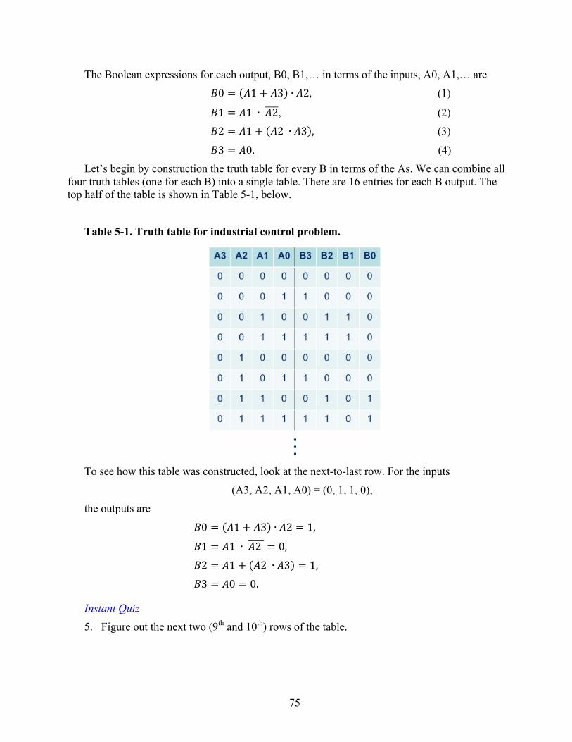
75
The Boolean expressions for each output, B0, B1,… in terms of the inputs, A0, A1,… are
𝐵0 = 𝐴1+ 𝐴3 ∙ 𝐴2, (1)
𝐵1 = 𝐴1 ∙ 𝐴2, (2)
𝐵2 = 𝐴1+ 𝐴2 ∙ 𝐴3 , (3)
𝐵3 = 𝐴0. (4) Let’s begin by construction the truth table for every B in terms of the As. We can combine all
four truth tables (one for each B) into a single table. There are 16 entries for each B output. The top half of the table is shown in Table 5-1, below.
Table 5-1. Truth table for industrial control problem.
To see how this table was constructed, look at the next-to-last row. For the inputs
(A3, A2, A1, A0) = (0, 1, 1, 0), the outputs are
𝐵0 = 𝐴1+ 𝐴3 ∙ 𝐴2 = 1,
𝐵1 = 𝐴1 ∙ 𝐴2 = 0,
𝐵2 = 𝐴1+ 𝐴2 ∙ 𝐴3 = 1, 𝐵3 = 𝐴0 = 0.
Instant Quiz 5. Figure out the next two (9th and 10th) rows of the table.

76
Next, take each 4-tuple, (B3, B2, B1, B0), and convert it into it’s equivalent hexadecimal number. For example, for the next-to-last row in Table 5-1, this gives 0101 = $5. The full list for all 16 entries in the table looks like this
$0, $8, $6, $E, $0, $8, $5, $D, $0, $8, $6, $E, $5, $D, $5, $D.
Now create your lookup table (suppose we start it at address $5000, etc.).
org $5000 dc.b $0, $8, $6, $E, $0, $8, $5, $D, $0, $8, $6, $E, $5, $D, $5, $D
Finally add the code org $4000 ; or wherever you want to put it ldx #$5000
forever: ldaa PORTA anda #%00001111 ; this zeros out the high nibble movb A, X, PORTB bra forever
So, what does this code do? First it loads the number $5000 into X. This is followed by a loop beginning with the label, forever. The first instruction in the loop loads Accumulator A with the number at Port A. The next line (anda) zeros out the high nibble. This is optional but it's a good idea in case somehow one of the high bits is set (for example, if you do not ground the bits of the high nibble, they might float high, or a piece of wire falls on your board and shorts a pin to Vcc). The next line is the key to what’s going on. The addressing mode is Accumulator Offset/Extended. The number that will be moved to Port B is the number in the address determined by the sum of the number in Accumulator A (the number that was loaded from Port A) plus the number in X, which is $5000 (from the ldx #$5000 instruction on line 2).
To see how this works, let’s look again at the next-to-last line in Table 5-1. The input bits at Port A are A3, A2, A1, A0 = 0, 1, 1, 0, respectively. %0000 0110 = $6. The number that will be moved to Port B is the number in address $5006. This number, from the lookup table, is $5; in binary the number is %0000 0101, and the low four bits are the correct values for B3 through B0.
The code above is 9 lines long. Compare this with the original code to do just one of the output bits, B1. This code was 14 lines long.
One note—you can type in the lookup table (starting with the org $5000 directive) anywhere you want and, in particular, you can put it before the instructions starting at $4000. However, if you decide to list it first, CodeWarrior might complain. It will still run but you might not see your code in the resulting Debug window.
If you like, you can let CodeWarrior figure out where to put the lookup table. You can do this using a label with the dc.b directive. Here’s how:
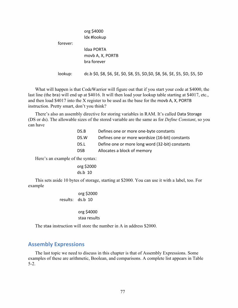
77
org $4000 ldx #lookup
forever: ldaa PORTA movb A, X, PORTB bra forever lookup: dc.b $0, $8, $6, $E, $0, $8, $5, $D,$0, $8, $6, $E, $5, $D, $5, $D
What will happen is that CodeWarrior will figure out that if you start your code at $4000, the last line (the bra) will end up at $4016. It will then load your lookup table starting at $4017, etc., and then load $4017 into the X register to be used as the base for the movb A, X, PORTB instruction. Pretty smart, don’t you think?
There’s also an assembly directive for storing variables in RAM. It’s called Data Storage (DS or ds). The allowable sizes of the stored variable are the same as for Define Constant, so you can have
DS.B Defines one or more one-‐byte constants DS.W Defines one or more wordsize (16-‐bit) constants DS.L Define one or more long word (32-‐bit) constants DSB Allocates a block of memory
Here’s an example of the syntax:
org $2000 ds.b 10
This sets aside 10 bytes of storage, starting at $2000. You can use it with a label, too. For example
org $2000 results: ds.b 10
org $4000 staa results
The staa instruction will store the number in A in address $2000.
Assembly Expressions The last topic we need to discuss in this chapter is that of Assembly Expressions. Some
examples of these are arithmetic, Boolean, and comparisons. A complete list appears in Table 5-2.

78
Table 5-2. Assembly expressions.
You can use Assembly expressions to help self-document your program. Also, you can use them to make it more easily modifiable. As an example, suppose you want to control the temperature of a room to within ±2C of normal room temperature (20C). Suppose, also, that your temperature sensor produces an 8-bit temperature value and is attached to Port A. You might start with the following equ directives
roomTemp: equ 20 highTemp: equ roomTemp + 2 lowTemp: equ roomTemp -‐ 2
roomTemp + 2 and roomTemp -‐ 2 are assembler expressions that define the temperatures at
which you might want to turn on the air conditioner or heater. Now follow this at some point by the code
continue ldaa PORTA cmpa #highTemp ; compare temperature to highTemp bgt turnOnAC ; if result of comparison is > 0 branch ; branch to routine that turns on AC
cmpa #lowTemp ; next, compare temperature to lowTemp blt turnOnHeater ; if result is < 0 branch to code that ; turns on heater
The ability to use assembler expressions in this way has two nice advantages. First, it makes clear what we are doing. Second, we can make global changes quickly. Suppose we decide that to save power we are willing to allow a ±3C degree temperature swing before turning on heating or air conditioning. We just have to make the change in the assembly expressions and it changes the values everywhere the labels appear.
We can also use expressions in instructions. For example, in this code, which we looked at a bit earlier
79
org $2000 results: ds.b 10
org $4000 staa results
we could have written staa results+3
in which case the contents of A would be stored in address $2003. It’s important to note that assembly expressions are evaluated by CodeWarrior during compilation, and not executed by the microcontroller during runtime. What this means is that the instruction staa results+3 is equivalent to staa $2003; there is no actual addition of $2000 plus 3 that goes on while the microcontroller is running.
Instant Quiz 6. Given the code below var1: equ %00110110
var2: equ $0f
comp1: equ !var1 prod: equ var1 * var2 var1ANDvar1: equ var1&var2 var1ORvar2: equ var1/\var2
find the values of a) comp1 b) prod c) var1_AND_var1 d) var1_OR_var2
Instant Quiz Answers 1. a) Extended, Indexed (all types) b) The N bit is cleared, the Z bit is set if the resulting byte is all zeros, the V bit is the
Exclusive-OR of N and the C bit, and the C bit is the value of the LSB of the byte before the shift. The other bits are unaffected.
2. ; Fragment 1 ldaa #$FF ; Load IMM takes 1 clock cycle (P) staa $03 ; Store DIR takes 2 clock cycles (Pw) ; total time for 3 clock cycles @ 2 MHz = 1.5 µs
80
; Fragment 2
movb #$FF, $03 ; movb IMM/EXT takes 4 clock cycles (OPwP) ; total time for 4 clock cycles = 2.0 µs
; Fragment 1 is half a microsecond faster. Not much, but if you’re running it ; several thousand times in a loop it starts to add up.
3. a) %11110010 (= -1410). The original number was -5610, and -56/4 = -14, so the answer makes sense.
b) %00100000 = 3210 ≠ -56 x 4.
4. After first shift: %01100101; C = 1 After second shift: %10110010; C = 1
After third shift: %01011001; C = 0. 5.
6. a) comp1 = 00110110 = %11001001
b) prod = %00110110 x $f = 810 = %0000001100101010 = $032A
c) var1_AND_var2 = %00000110
d) var1_OR_var2 = %00111111
Homework 1. For the following instructions, find which addressing modes are supported (note that you
can find all these instructions at the end of the CPU12 Reference Manual): INCA, BITB, DEC, BCLR, MOVB, STAA. Also find how the condition code bits are affected.
2. Write a code fragment that directs the assembler to set aside four bytes in RAM for the
variable named “output” and stores the numbers 1 through 4 in byte form in ROM as data constants “input” (don’t forget to use the appropriate ORG statements).
3. Write a code fragment that stores the sines of the angles 0 through 10 degrees in one-
degree increments in addresses $5000 through $500A. The sines should be stored as 3-

81
digit integers since the microcontroller can’t do floating point arithmetic (i.e., the sine of 5o = 0.087; this should be stored as 087).
4. Modify your code to do the following:
a) Read a byte from Port H b) Clear bits 4-7 of the byte read from Port H c) Use the resulting 4-bit number to pick the corresponding number from the list
above and move it to Port B (e.g., if the number at Port H is $5, copy the number in address $5005 to Port B).
d) Repeat steps (a) through (c) forever.
Remember to set up the DDRs for Ports H and B. 5. Give the result for Q1 through Q4 in hexadecimal for each of the following assembler
expressions: MS_MASK: EQU %11110000 LS_MASK: EQU %00001111 MOST: EQU 255 NEG: EQU -‐128 SIX: EQU 6 TEN: EQU 10
a) Q1: DC.B SIX+TEN b) Q2: DC.B SIX | TEN c) Q3: DC.B MOST ^ LS_MASK d) Q4: DC.B ~MS_MASK
6. For your code in problem 4, use the Reference Manual to determine how many bus clock
cycles the code takes to run one time around (including the branch).

82
Chapter 6. Timing and Pulse Width Modulation
The only reason for time is so that everything doesn’t happen at once.
- A. Einstein
So far, everything we’ve done has not had any time-dependent behavior. That is, we’ve implemented software versions of simple combinatorial logic gates or truth tables whose outputs change when their inputs change. The outputs change as fast as the microcontroller can run the code. We can’t yet, for example, do things like having the outputs wait a fixed time interval after the inputs change. A practical example might be having a light turn off a minute after you turn off the switch to allow you time to get out of a room.
In fact, many applications require specialized timing behavior. Some examples are
− time delays—this is the kind of thing we just talked about with the light switch.
− frequency measurements—to measure the frequency of an incoming signal you have to measure how many times the signal changes in a fixed time interval.
− periodic events—you might want to perform some task at regular time intervals, such as checking an external sensor every 100 ms.
− complex waveform generation—this involves generating a signal that can vary in frequency or shape in an irregular way over time. Some applications are sending bit patterns over a network, controlling a servomotor in a robot, or making a simple light dimmer.
There are lots more. In this chapter we will address the question of how you introduce complicated time behavior
into your microcontroller code. The simplest way to do this is with something called a “delay loop,” which we’ll talk about next. We’ll then describe the HCS12 timing module and then look in some detail at the module that generates a pulse-width modulated signal. Along the way we’ll describe how to use “subroutines” to generate variable delays at multiple points in your code.
Delay Loops For some of the applications above you can use simple “delay loops.” To see how these work,
look at the following code:
83
ldy #6000 ; 2 loop: dey ; 1 this decrements the Y Register bne loop ; 3 if loop is taken, 1 if not
What does it do? Well, basically nothing. The important thing is that it takes some time to do
it, generating a delay. The code loads the Y Register with the number 600010 and then just loops 6000 times as it
decrements the Y Register using the dey instruction. The numbers in the comments are the number of bus clock cycles each instruction takes (from the reference manual). So, how long is the delay?
The code takes 2 + (1+3) x 6000 +1 = 24,003 clock cycles to run,
The bus runs at 24 MHz, so each bus clock cycle takes 1/24 x 10-6 seconds, So the code takes ~1 ms to run.
This is an example of a 1 ms delay loop. To get longer delays, just embed this in an outer timing loop:
ldx #1000 outer_loop:
ldy #6000 ; 2 loop: dey ; 1 this decrements the Y Register bne loop ; 3 if loop is taken, 1 if not
dex ; this decrements the X register bne outer_loop
The instructions in blue are the original 1 ms code. What we’ve done is just to embed the
1 ms code in an outer loop that runs 1000 times, resulting in a 1 second delay. In this way you can get a delay of any size you want.
Instant Quiz
1. Write the code to get a 10-second delay.
The delay loop written this way won’t give you exactly a 1 ms delay because of the time needed to do the additional branching. If precision is important, you will need to connect your microcontroller to an oscilloscope and tweak your code to give you the precision you want. You do this by adding or subtracting to the number of loops you do. If you still don’t get the precision

84
you want you can strategically add a number of no op instructions (NOP). NOP stands for “no operation.” These don’t do anything but they take one clock cycle to execute.
It’s often the case that you are using the X or Y Registers for something else in your program. When this happens you can just use an ordinary memory address as your counter. The only problem is that in a memory location you only have 8 bits so you can only count down from 28-1 = 255. In the example above you need to count down from 1000. The workaround is to use two nested loops with two different memory locations as counters. Here’s one way to do it
movb #4, $2001 outer_loop:
movb #250, $2000 inner_loop:
ldy #6000 ; 2 loop: dey ; 1 this decrements the Y Register bne loop ; 3 if loop is taken, 1 if not
dec $2000 ; this decrements address $2000 bne inner_loop dec $2001 bne outer_loop
What is going on here is that you are running the millisecond delay 250 times using the inner loop, producing a 250-ms delay, and then running the 250-ms delay 4 times to give a one second delay. You might take a minute and trace how the logic flows.
If you need to generate delays at several different points in your code, it’s easier to write the code for the delay once and then call it at each point in your code that it’s needed using a “subroutine.” A subroutine (in C/C++ it’s called a “function) is a piece of code that could function independently to do some specific task but you stash it somewhere in the memory and then “call” it where you need it. You call the subroutine with a Jump to Subroutine (jsr) instruction (you could also use a Branch to Subroutine, or bsr instruction), which tells the microcontroller to jump to the location containing the first instruction of the subroutine and start running the code there. At the end of your subroutine code you have to add a Return from Subroutine (rts) instruction. This tells the microcontroller to return to where it was before the call and continue executing the main code. You can indicate the place where you’ve put the subroutine either with the actual address or using a label.
As a simple example, suppose you want to turn on an output (say B0), wait for one millisecond, then turn it off for one millisecond, and then repeat the process forever. If you connected your output to a light emitting diode you would have a 500 Hz flasher. Here’s the code to do it, using an address:

85
org $4000 ; this is the start of your main program bset DDRB, %00000001 ; don’t forget to set up your DDR forever: bset PORTB, %00000001 ; this turns on the output jsr $5000 ; this jumps to the 1 ms delay routine bclr PORTB, %00000001 ; this turns off the output
jsr $5000 ; this delays 1 ms again bra forever ; this loops the code forever
org $5000 ; here’s the start of your subroutine
ldy #6000 ; loop: dey ; bne loop ; rts ; this returns you to the main
program
Notice that our main code starts at $4000 and we’ve put the subroutine at $5000. The jsr
instruction tells the microcontroller to jump to address $5000. Inside the “forever” loop you’re just turning on the output, then jumping to your millisecond delay, then turning off the output and delaying for a millisecond again. Then you loop back to forever to repeat the process. Also note the rts instruction at the end of the subroutine. If you forget to include this the microcontroller will just continue trying to execute whatever is in the memory following the subroutine, which could be anything. It will never get back to your main program.
Using a subroutine saves you writing the delay loop twice. This might not seem like a big deal since you could just cut and paste it the second time but you would have to change the loop label to something else to avoid duplicate labels. This is an inconvenience that grows in size with the number of times you call the subroutine in your code. It also uses up more memory—a lot of memory if your subroutine is big.
Here’s how you can call a subroutine using a label
org $4000 ; this is the start of your main program bset DDRB, %00000001 ; don’t forget to set up your DDR forever:
bset PORTB, %00000001 ; this turns on the output jsr delay_1_ms ; this delays 1 ms bclr PORTB, %00000001 ; this turns off the output
jsr delay_1_ms ; this delays 1 ms again bra forever ; this loops the code forever

86
delay_1_ms: ; here’s the start of your millisecond
ldy #6000 ; delay subroutine loop: dey bne loop rts ; this returns you to the main program
What we’ve done is to identify the subroutine with the label delay_1_ms. Then we just replace jsr $5000 in the original code with jsr delay_1_ms. CodeWarrior will put the subroutine right after your main code and just use the address where the first instruction of the subroutine winds up to replace the label delay_1_ms everywhere it appears with an instruction. Of course, you can use an org directive followed by the label to force CodeWarrior to put the subroutine anywhere you like if you want to.
Suppose you now want to do something a little more complicated, such as turning on the output for one millisecond but then turning it off for five milliseconds to produce a signal with a 20% duty cycle (the duty cycle is the ratio of the on time to the period). You could write a second delay loop of five-milliseconds, or you could just call the one-millisecond delay loop five times in a row; either with 5 successive jsr instructions or by putting a single jump instruction in a loop of five iterations.
This is what the loop part of the code would look like (the rest is the same as above):
forever: bset $1, %00000001 ; this turns on the output jsr delay_1_ms ; this delays 1 ms bclr $1, %00000001 ; this turns off the output
ldaa #5 ; *this loop delays 1 ms 5 times
loop5times: jsr delay_1_ms ; * deca ; * bne loop5times ; *
bra forever ; this loops the code forever
We’ve used Accumulator A as our counter but you could just as easily used an index register or a memory address.
As an aside, most programmers accumulate a collection of subroutines that they use regularly and can just paste into any code they’re writing. To get a range of possible timing combinations they might have a millisecond delay and also separate microsecond, 10-microsecond, and hundred-microsecond delays so they can plug in whatever is easiest and most efficient to use.

87
The HCS12 Timing Module Implementing delays and other timing functions using delay loops has three problems. First,
as we mentioned, it’s not really accurate unless you fine-tune it. Second, the processor is always busy executing the delay instructions, so it can’t do anything else, such as processing incoming data. You could embed some of these functions into the delay loop but then you have to take into account the time they take when figuring out how to get the correct delay timing. Third, it’s difficult to generate complex wave functions this way. In the example we just did in which we constructed an on/off flasher, imagine how difficult it would be if we needed to change the duty cycle frequently.
To avoid these problems, most microcontrollers have a dedicated on-board timing module. These modules support many functions in addition to simple time delays, such as event counting or timing, frequency measurements, periodic event generation (such as interrupts), or complex waveform generation. Best of all, they are designed to run in the background. What this means is that you set the module up by writing information to its control registers and then it continues to do its job without intervention from the CPU. This frees the CPU to run the rest of your program.
Figure 6-1 shows a block diagram of the HCS12 Standard Timer Module (TIM). The timing module runs off the system bus clock, which you can see at the upper left. A 7-stage prescaler can be used to divide the bus clock by any power of two up to 27 = 128, including 20 = 1. You get to pick what power of 2 to divide by.
Figure 6-1. The HCS12 Standard Timer Module (TIM).
88
The divided-down clock is sent to a 16-bit free running counter (TCNT) that counts pulses from the prescaler. It starts at $0000 and runs up to $FFFF, then resets and starts again on the nest pulse. Each time it resets it sets a flag, the Timer Overflow Flag (TOF), to let you know that this has happened. You can check if the overflow has occurred in two ways. First, you can periodically monitor the TOF bit manually. Second, you can enable an interrupt that will be generated when it happens.
These functions, and many others, are set up by writing to control registers, in the same way you write to the DDRs to set up parallel I/O ports. The difference is that it’s a bit more complicated and there are more registers to write to. The power of 2 used in the prescalar is defined by the lowest three bits of register TSCR2 (for Timer System Control Register 2), located at address $004D. For example, the lines
bset TSCR2, %00000101 bclr TSCR2, %00000010
makes the three bits of the prescaler value 101 = 5, so the bus clock will be divided by 25 =
32. If your bus clock is running at 24 MHz, the TCNT counter will be incrementing at 24 MHz ÷ 32 = 750 KHz. By the way, you can’t easily use a movb #%00000101, TSCR2 instruction because some of the other bits in the register are used for something else and you may be altering them.
The TCNT register itself is located at addresses $0044:$0045 (remember, it’s a 16-bit register). You can read TCNT anytime you want, for example with an ldd (Load D) instruction. You can’t use two ldaa instructions to read the high byte and then the low byte because the value in the low byte will have changed in the time it takes to read the high byte.
An example of a simple thing you can do with this is to time the time interval between two events. You set up the prescaler value to give you the time accuracy you want and then just read the number in TCNT when each event happens. The difference times the prescaled clock period is the time interval between events.
Instant Quiz
2. The speed of a car is measured by the time it takes for the car to break two laser beams 1 m apart. You’re using an HCS12 microcontroller to determine the time. The bus clock is running at 8 MHz and the last three bits of the prescaler (at $004D) are 011. The two values read from TCNT as the car breaks each beam successively are %0000000100101110 and %0001010010110110, respectively. Assuming the counter hasn’t overflowed, what is the time interval between the breaks in the two beams, and how fast is the car going?
Another useful register is the Modulus Down-Counter. It doesn’t appear in Figure 6-1 because it’s isn’t available in all members of the HCS12 family. When it is available, it’s part of something called the Enhanced Capture Timer (ECT) Module.
The way the Modulus Down-Counter works is that you load a number into the Modulus Down-Counter Count Register (MCCNT) at address $0076:$0077 (it’s a 16-bit register) and it begins to count down using the bus clock divided by a 4-bit prescalar. This prescalar can be set

89
to divide the bus clock by 1, 4, 8, or 16. When the counter counts down to zero you have the option to either have it stop or continuously reload itself and count down again. Either way, once it hits zero a flag is raised in the MCFLG register. The flag is in bit 7 and the other bits aren’t used (they’re all zero by default), so you could, for example load an accumulator from MCFLG and test the Z bit to see if the counter has reached zero.
You also have the option of having the counter generate an interrupt each time it reaches zero. This allows you to do some task periodically, such as monitor an external sensor without the CPU doing any of the timing.
Setting up the counter is a little more complicated than setting up the DDRs for a parallel port. You set the counter up by writing to its control register, MCCTL, at address $0066. Figure 6-2 shows the function of each bit in this register. To use the Modulus Down Counter you have to do the following (refer to the figure):
1. Enable the interrupt (assuming you want to generate an interrupt) by setting Bit 7 (Modulus Counter Underflow Interrupt Enable). If you don’t want to use interrupts just clear this bit.
2. Enable Modulus Mode by setting Bit 6 (Modulus Mode Enable). This tells the counter to reload itself and begin counting down again each time it reaches 0. If you clear this bit the counter will count down once and stop.
Figure 6-2. Description of the bits in the MCCTL register.
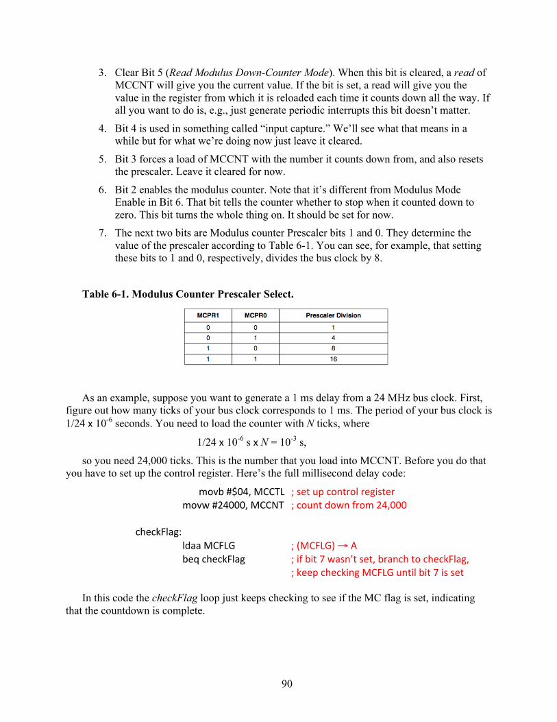
90
3. Clear Bit 5 (Read Modulus Down-Counter Mode). When this bit is cleared, a read of MCCNT will give you the current value. If the bit is set, a read will give you the value in the register from which it is reloaded each time it counts down all the way. If all you want to do is, e.g., just generate periodic interrupts this bit doesn’t matter.
4. Bit 4 is used in something called “input capture.” We’ll see what that means in a while but for what we’re doing now just leave it cleared.
5. Bit 3 forces a load of MCCNT with the number it counts down from, and also resets the prescaler. Leave it cleared for now.
6. Bit 2 enables the modulus counter. Note that it’s different from Modulus Mode Enable in Bit 6. That bit tells the counter whether to stop when it counted down to zero. This bit turns the whole thing on. It should be set for now.
7. The next two bits are Modulus counter Prescaler bits 1 and 0. They determine the value of the prescaler according to Table 6-1. You can see, for example, that setting these bits to 1 and 0, respectively, divides the bus clock by 8.
Table 6-1. Modulus Counter Prescaler Select.
As an example, suppose you want to generate a 1 ms delay from a 24 MHz bus clock. First, figure out how many ticks of your bus clock corresponds to 1 ms. The period of your bus clock is 1/24 x 10-6 seconds. You need to load the counter with N ticks, where
1/24 x 10-6 s x N = 10-3 s,
so you need 24,000 ticks. This is the number that you load into MCCNT. Before you do that you have to set up the control register. Here’s the full millisecond delay code:
movb #$04, MCCTL ; set up control register movw #24000, MCCNT ; count down from 24,000 checkFlag: ldaa MCFLG ; (MCFLG) → A beq checkFlag ; if bit 7 wasn’t set, branch to checkFlag,
; keep checking MCFLG until bit 7 is set In this code the checkFlag loop just keeps checking to see if the MC flag is set, indicating
that the countdown is complete.

91
Instant Quiz 3. Explain the effect of each bit loaded into the MCCTL register in the example above.
The biggest delay we can get this way is by loading MCCNT with 65,535. This corresponds
to a delay of about 2.7 ms. To get longer delays we just divide the bus clock by the prescaler value determined by bits 1 and 0 in MCCTL. For example, in the code above if we again loaded MCCNT with 24,000 but changed the first line to movb #$06, MCCTL, the prescalar would be set to 8, and we would get an 8 ms delay.
Instant Quiz 4. Write the code to generate a 20 ms delay.
Now you can do all sorts of complicated things. For example, suppose you want to generate a 100 Hz square wave at bit 0 of Port B. You just change the code above to generate a 5 ms delay and then put it in a loop that runs forever, but each time you loop, complement bit B1. This turns the bit on for 5 ms, then off for 5 ms, resulting in a 10 ms period (100 Hz). Here’s the code:
movb #1, DDRB ; make Port B bit 1 output movb #1, PORTB ; initialize bit 1 movb #$45, MCCTL ; enable down counter, set prescalar to divide by 4 movw #30000, MCCNT checkFlag: ldaa MCFLG beq checkFlag ; loop until flag is set com 1 ; flip bit 0 bset MCFLG, $80 ; you have to clear the flag to begin again bra checkFlag
There are three things you should notice about this code: 1. By moving $45 (%01000101) to MCCTL in the third line we’ve set bit 6; this enables
the Modulus mode, which means MCCNT is automatically reloaded and starts counting down each time the count reaches zero
2. You have to clear the flag for the counter to start counting down again; we do this by writing 1 to bit 7 of MCFLG in the next to last line
3. We flip bit 0 of Port B using a Complement instruction (com 1). This flips all the bits in address $1, but since we’ve only made bit 0 an output and the rest inputs, the other bits won’t be affected. If you want to use any of the other bits as outputs for other purposes you can’t do it this way because the other bits will be flipped, too. You need

92
to do the exclusive-OR trick that you learned before. Just replace the com 1 instruction with the following code:
ldaa 1 ; load A with the current number in Port B eora #%00000001 ; flip bit 0, leave the others unchanged staa 1 ; store the new number back in Port B
The problem with doing delays in this way is that the processor is still occupied full time with running the code, so the only advantage it has over a simple delay loop is convenience (and a little better accuracy). To free the processor for other work while the counter is counting, you need to employ the interrupt function. We’ll see how to do this in the next chapter. For now, we’ll just briefly cover some of the other functionality of the timing module. Then we’ll finish up with a detailed description of the pulse width generation module.
Looking again at Figure 6-1, we see eight channels of multiplexed input capture and output compare functions. Input-capture latches the contents of TCNT when a specified event occurs. This could, for example, be used to time the period between two events. We described a way to do this earlier by reading the contents of TCNT at each event, but the Input capture function does this in background without having to use the CPU. The 16-bit Pulse Accumulator counts events arriving in a defined time interval. This can be used to find the frequency of an incoming signal. Each Input Capture register can generate an independent interrupt. Output-compare compares the value in the timer counter with that of the output-compare register. Each channel can also generate an interrupt when they are equal. Each of the 8 channels can be connected to an external bidirectional pin via Port T.
All functions are controller via timer registers in the same way as we saw for the modulus down counter. The devil, of course, is in the details. You can see how involved the process of setting up a register to do what you want can be. You basically have two choices when confronted with the need to do this for a timer function you haven’t used before. You can pour over the extremely dry description of the control registers in the reference manual or some textbook to see how the individual bits should be programmed, or you can search the web to see how other people have solved a similar problem. Most people take the more sensible of the two approaches. If you ever have to do this you will quickly learn the benefits of using a popular and strongly supported microcontroller family.
The HCS12 Pulse-‐Width Modulation Module Now we are going to look at the Pulse-Width Modulation (PWM) module in some detail, but
first, what exactly is “pulse-width modulation? Consider the periodic signal in Figure 6-3. The period is how long it takes for the signal to repeat itself, i.e., turn on and off once. The inverse of the period is the frequency.
The ratio of the on-time to the total period, expressed as a percentage, is the duty cycle, tD:
tD = ton/tperiod x 100%.

93
Figure 6-3. Time signal for measuring duty cycle.
If the duty cycle changes over time the signal is said to be pulse width modulated. If you also change the period (frequency) over time you can generate some really complex waveforms. Some applications are telecommunications, robot motor controllers, or even simple light dimmers. As an example, most standard servomotors, often used in robotic applications, are controlled using a 20 ms (50 Hz) square wave signal. The angle through which the motor will turn is directly proportional to the duty cycle. The HCS12 PWM module allows you to change both the duty cycle and the frequency (period) on the fly.
Figure 6-4 shows a functional diagram of the module. The HCS12 has an 8-channel PWM module. Each channel has a period register, a duty cycle register, a control register, and a dedicated counter. The basic operation requires only two inputs—period and duty cycle— plus Enable to generate the PWM waveform automatically. There are a lot of other control features that you can use but for now we’ll just focus on the minimum you need to get up and running.
Figure 6-4. The HCS12 Pulse-Width Modulation module.

94
There are four possible clock sources for the PWM module: Clock A, Clock SA, Clock B,
and Clock SB. Clock A and Clock B are derived by dividing the bus clock by 2n, where n can range from 0 to 7. You can set the divisor independently for each clock. Clock SA is derived by dividing clock A by an even number ranging from 2 to 512. Similarly, Clock SB is derived by dividing the clock B by an even number ranging from 2 to 512. Clocks SA and SB also can be set independently by writing to an 8-bit register. The number that you write is multiplied by 2 to get the range 2 to 512 for the divisor.
To set up the PWM module you do the following by writing to the appropriate registers: 1. Select Clock A, B, SA, or SB (PWMCLK)
2. Select prescale value (PWMPRCLK) 3. Set period (PWMPER)
4. Select duty cycle (PWMDTY) 5. Enable output for selected channel (PWME)
Optionally, you can enable active high polarity of the output signal by writing to register PWMPOL, and/or align the edge of the PWM signal with the left edge or center of the bus clock by writing to register PWMCAE.
Clock A is determined by dividing the bus clock by the prescale value. The prescale value is 2n, where n is a 3-bit number written to register PWMPRCLK (PWM Prescale Clock Register) at memory location $A3. Figure 6-5 shows the bit definitions in this register.
Figure 6-5. Register PWMPRCLK bit definitions.
Three bits each are allocated for the prescalers for Clocks A and B; the two most significant bits are not used. To see how it works, suppose you execute the instruction
movb #%00000110, PWMPRCLK
This makes (B2, B1, B0) = (0, 0, 0) → 0; and (A2, A1, A0) = (1, 1, 0) → 6, so Clock B is the bus clock divided by 20 = 1 and Clock A is the bus clock divided by 26 = 64. If the bus clock is 8 MHz, clock A is 8/64 MHz = 125 KHz (corresponding to an 8 µs period).
You can also get finer control using Clock SA (or Clock SB), which divides the Clock A (Clock B) signal by 2 times the number in register PWMSCLA, at address $A8:
Clock SA = Clock A / (2 * PWMSCLA), i.e., 0 to 512, even numbers only.
If the number in PWMSCLA is 0, Clock A is used directly (that is, you don’t divide by 0). You select between using just Clock A (or B) or using Clock A (B) and Clock SA (SB) by
writing to register PWMCLK. This register is shown in Figure 6-6. To see how this works, if you want to select just Clock A for output 0, you write a 0 to bit 0. To select Clock SA you write a 1.
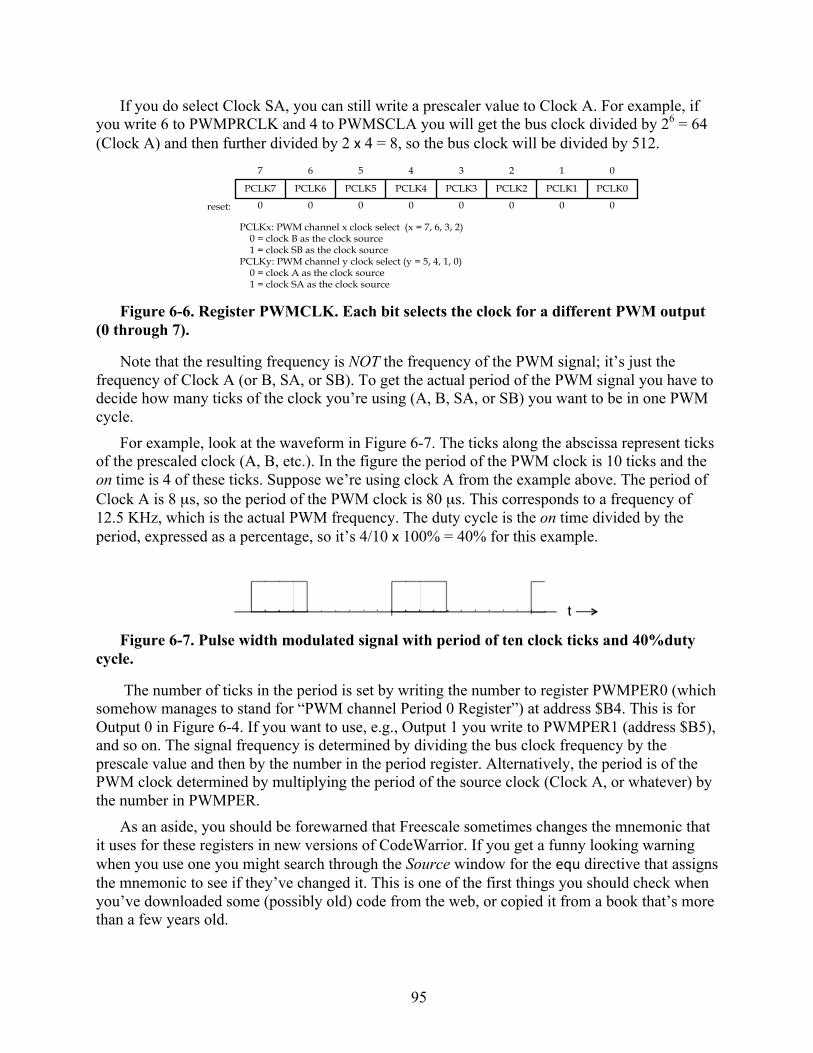
95
If you do select Clock SA, you can still write a prescaler value to Clock A. For example, if you write 6 to PWMPRCLK and 4 to PWMSCLA you will get the bus clock divided by 26 = 64 (Clock A) and then further divided by 2 x 4 = 8, so the bus clock will be divided by 512.
Figure 6-6. Register PWMCLK. Each bit selects the clock for a different PWM output
(0 through 7).
Note that the resulting frequency is NOT the frequency of the PWM signal; it’s just the frequency of Clock A (or B, SA, or SB). To get the actual period of the PWM signal you have to decide how many ticks of the clock you’re using (A, B, SA, or SB) you want to be in one PWM cycle.
For example, look at the waveform in Figure 6-7. The ticks along the abscissa represent ticks of the prescaled clock (A, B, etc.). In the figure the period of the PWM clock is 10 ticks and the on time is 4 of these ticks. Suppose we’re using clock A from the example above. The period of Clock A is 8 µs, so the period of the PWM clock is 80 µs. This corresponds to a frequency of 12.5 KHz, which is the actual PWM frequency. The duty cycle is the on time divided by the period, expressed as a percentage, so it’s 4/10 x 100% = 40% for this example.
Figure 6-7. Pulse width modulated signal with period of ten clock ticks and 40%duty
cycle.
The number of ticks in the period is set by writing the number to register PWMPER0 (which somehow manages to stand for “PWM channel Period 0 Register”) at address $B4. This is for Output 0 in Figure 6-4. If you want to use, e.g., Output 1 you write to PWMPER1 (address $B5), and so on. The signal frequency is determined by dividing the bus clock frequency by the prescale value and then by the number in the period register. Alternatively, the period is of the PWM clock determined by multiplying the period of the source clock (Clock A, or whatever) by the number in PWMPER.
As an aside, you should be forewarned that Freescale sometimes changes the mnemonic that it uses for these registers in new versions of CodeWarrior. If you get a funny looking warning when you use one you might search through the Source window for the equ directive that assigns the mnemonic to see if they’ve changed it. This is one of the first things you should check when you’ve downloaded some (possibly old) code from the web, or copied it from a book that’s more than a few years old.
7 6 5 4 3 2 1 0
PCLK7 PCLK6 PCLK5 PCLK4 PCLK3 PCLK2 PCLK1 PCLK0
reset: 0 00 0 0 0 0 0
Figure 8.42 PWM clock select register (PWMCLK)
PCLKx: PWM channel x clock select (x = 7, 6, 3, 2) 0 = clock B as the clock source 1 = clock SB as the clock sourcePCLKy: PWM channel y clock select (y = 5, 4, 1, 0) 0 = clock A as the clock source 1 = clock SA as the clock source
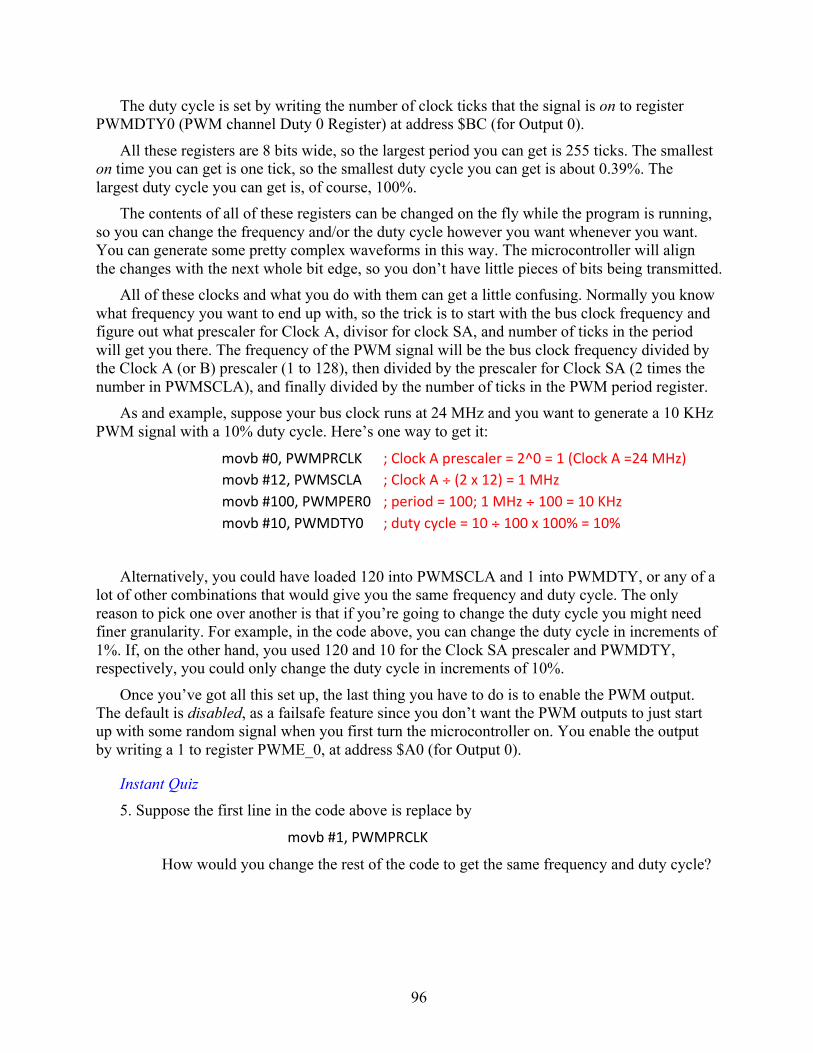
96
The duty cycle is set by writing the number of clock ticks that the signal is on to register PWMDTY0 (PWM channel Duty 0 Register) at address $BC (for Output 0).
All these registers are 8 bits wide, so the largest period you can get is 255 ticks. The smallest on time you can get is one tick, so the smallest duty cycle you can get is about 0.39%. The largest duty cycle you can get is, of course, 100%.
The contents of all of these registers can be changed on the fly while the program is running, so you can change the frequency and/or the duty cycle however you want whenever you want. You can generate some pretty complex waveforms in this way. The microcontroller will align the changes with the next whole bit edge, so you don’t have little pieces of bits being transmitted.
All of these clocks and what you do with them can get a little confusing. Normally you know what frequency you want to end up with, so the trick is to start with the bus clock frequency and figure out what prescaler for Clock A, divisor for clock SA, and number of ticks in the period will get you there. The frequency of the PWM signal will be the bus clock frequency divided by the Clock A (or B) prescaler (1 to 128), then divided by the prescaler for Clock SA (2 times the number in PWMSCLA), and finally divided by the number of ticks in the PWM period register.
As and example, suppose your bus clock runs at 24 MHz and you want to generate a 10 KHz PWM signal with a 10% duty cycle. Here’s one way to get it:
movb #0, PWMPRCLK ; Clock A prescaler = 2^0 = 1 (Clock A =24 MHz) movb #12, PWMSCLA ; Clock A ÷ (2 x 12) = 1 MHz movb #100, PWMPER0 ; period = 100; 1 MHz ÷ 100 = 10 KHz movb #10, PWMDTY0 ; duty cycle = 10 ÷ 100 x 100% = 10%
Alternatively, you could have loaded 120 into PWMSCLA and 1 into PWMDTY, or any of a lot of other combinations that would give you the same frequency and duty cycle. The only reason to pick one over another is that if you’re going to change the duty cycle you might need finer granularity. For example, in the code above, you can change the duty cycle in increments of 1%. If, on the other hand, you used 120 and 10 for the Clock SA prescaler and PWMDTY, respectively, you could only change the duty cycle in increments of 10%.
Once you’ve got all this set up, the last thing you have to do is to enable the PWM output. The default is disabled, as a failsafe feature since you don’t want the PWM outputs to just start up with some random signal when you first turn the microcontroller on. You enable the output by writing a 1 to register PWME_0, at address $A0 (for Output 0).
Instant Quiz
5. Suppose the first line in the code above is replace by
movb #1, PWMPRCLK
How would you change the rest of the code to get the same frequency and duty cycle?
97
Finally, if this is all you want to do, you should write some code to stop the microcontroller from running through the rest of the memory and trying to execute whatever instructions it thinks it finds there. You could, for example, end your code with
forever: bra forever
There are a lot more registers in the PWM module that you can do some really complicated things with, but you now have everything you need to solve some fairly sophisticated control problems.
Instant Quiz Answers 1. ldx #10000
outer_loop:
ldy #6000 ; 2 loop: dey ; 1 bne loop ; 3 if loop is taken, 1 if not
dex bne outer_loop
2. The bus clock is divided by 23 = 8, so TCNT is incrementing 1 MHz. 1 MHz corresponds
to a 1 µs period. The difference in numbers read from TCNT is %0001010010110110 - %0000000100101110 = 500010.
So the time interval is 5000 µs, or 50 ms. The speed of the car is 20 m/s.
3. Bit 7 = 0; disables the interrupt Bit 6 = 0; the down counter will count down to 0 and stop, raising the flag
Bit 5 = 0; if you do a read from MCCNT you will get its contents rather than the number with which it is reloaded
Bit 4 = 0; no effect Bit 3 = 0; no effect
Bit 2 = 1; enables (turns on) the counter Bits 1 and 0 = 0; prescaler divides by 1

98
4. movb #$06, MCCTL ; prescalar is now set to divide by 8 movw #60000, MCCNT ; count down from 60,000 checkFlag: ldaa MCFLG ; (MCFLG) → A beq checkFlag ; if bit 7 wasn’t set, branch to checkFlag,
; keep checking MCFLG until bit 7 is set ; you could also load MCCNT with 30,000 and set the prescalar to 26
5. Moving 1 to the Clock A prescaler register means “divide the bus clock by 21 = 2. There are a lot of combinations that will give the correct result. Here’s one:
movb #1, PWMPRCLK ; Clock A prescaler = 2^1 = 2 (Clock A = 12 MHz) movb #12, PWMSCLA ; Clock A ÷ 2 x 12 = 0.5 MHz movb #50, PWMPER0 ; period = 50, 0.5 MHz ÷ 50 = 10 KHz movb #5, PWMDTY0 ; duty cycle = 5 ÷ 50 x 100% = 10%
Note that it’s not easy to just change PWMSCLA to get the right answer since the number you load gets multiplied by 2.
Homework 0. Search the web for the MC9S12GC Family Reference Manual. Download it and skim
through Chapter 12 on PWM. Don’t get too crazy about it, though. 1. Write a short code fragment to implement a delay of one minute based on your
millisecond delay loop, then turn on an LED at Port B, bit 0. 2. Write the code necessary to generate a delay of 256 counts (0 to 255) and turn on an LED
at Port B for the first 115 counts, then turn it off for the remaining 140 counts. The cycle should repeat forever.
3. What values would you have to write to memory locations $b4 and $bc to generate a pulse with a duty cycle of 45%?
4. Suppose you have an 8 MHz bus clock. Write the code to generate a 1 KHz PWM signal with a 20% duty cycle. Note that if you want to use clock SA, the frequency is divided by Clock A/(2*PWMSCLA), where PWMSCLA is at address $08. Note also that you can do this just using Clock A.)

99
Chapter 7. Interrupts
In previous chapters we often alluded to the term interrupt as something that caused the microcontroller to stop what it was currently doing and instead begin to do something else, presumably something more important at the moment. In particular, in the last chapter we mentioned that many of the timer functions could be set up to generate an interrupt when some specified timing or counting sequence had completed. Other modules in the microcontroller can generate interrupts to notify the processor that they’ve completed a task or require attention. Some examples are the analog-to-digital converter module and the various communications modules. Interrupts can be triggered by some external event, as well, such as some sensor detecting a condition that required special attention (e.g., a fire alarm). Another external interrupt source is the Reset pin on the microcontroller chip. When this pin is toggled the microcontroller goes into a reset routine that might, for example, flush some part of its memory and start running your code from the beginning. There are also software-generated interrupts. The HCS12 has an swi instruction (Software Interrupt) that stops the current program and runs a special program that you write. You might use this to debug your program if you think it’s going off to some part of the code it shouldn’t be. To see if it’s actually going there you might drop in an swi instruction that tells the controller to run some special diagnostic.
In this chapter we’ll see how interrupts work in the HCS12 and how you use them. In particular, we’ll look at how you use two external interrupt pins, IRQ and XIRQ, and then we’ll examine how you use the interrupt connected to the MCCNT register that we talked about in the last chapter to generate periodic events. By the way, this is a good place to warn you that the term “IRQ” is used interchangeably to represent both the IRQ pin and an “Interrupt Request” generated by any of the other possible sources.
What are Interrupts and how do They Work? The industrial control example that we saw in Chapter 3 and then again in Chapter 5 (Figure
3-4) is an example of a “polling loop.” What this means is that you are constantly “polling” the inputs to see what the outputs should be. This wastes processor resources since the CPU is fully engaged in doing the sampling all the time. We saw the same problem with the delay loop of the last chapter. This is ok as long as that’s all you want to do, but suppose you want to do something like reading the output of a sensor every hundred milliseconds and using the CPU to process the data in between samples? The solution is to use an “interrupt.”
An interrupt is an unscheduled event that requires the processor to stop its normal operation and perform some special service related to the event. “Unscheduled” in this context means “not scheduled as part of the program the microcontroller is currently running.” It could be regularly scheduled in time, such as in the case of the sensor that is read every hundred milliseconds. In this sense the interrupt is said to be asynchronous with respect to the program that is running before the request is encountered.
An interrupt is initiated via an “Interrupt Request” (IRQ) that can be generated by one of the sources mentioned above (IRQ or XIRQ pins, various modules such as the timing module, or
100
software). The request is serviced via an “Interrupt Service Routine” (ISR). This is a program that you write and store somewhere in memory. When the ISR is finished responding to the request, the microcontroller returns to what it was doing before.
Some common uses of interrupts include:
− switching from one task to another
− asynchronous communications
− time-critical applications (e.g., alarms, emergency shutoffs, etc.)
− health checks
Health checks are particularly important. Because microcontrollers are often embedded in a system and expected to run autonomously for months and years, it is important to have a way to test the health of the system periodically. You could do this by setting up your own timer if you like, but the HCS12 provides a dedicated timer for this purpose. It’s called the Computer Operating Properly (COP) timer in the HCS12, but a more common name is Watchdog Timer. You can see it in Figure 1-5 on the left a little below the CPU12 block. You can set it up to generate an interrupt periodically and then design the ISR to check various registers or addresses to ensure that the program is stepping along properly.
Interrupt Types
Interrupts are handled by special circuitry in the microcontroller. They are classified by the method in which they are handled. There are two basic systems—polled and vectored. A polled interrupt system notifies the interrupt controller that a device is ready to be read or otherwise handled but does not indicate which device is making the request. The interrupt controller must poll (send a signal out to) each possible source of the IRQ in turn until it finds which one made the request. In a vectored interrupt system the IRQ includes the identity of the device sending the interrupt signal. The HCS12 uses vectored interrupts.
Each method has advantages and disadvantages. A polled interrupt system is simpler and uses fewer resources (circuitry, memory, power) on the chip. However, it’s slower due to the poling procedure. Vectored interrupt systems are much faster but use more resources.
Individual sources of interrupts (the IRQ pin, modulus down-counter, etc.) are also classified by whether they are “maskable” or “non-maskable.” A maskable interrupt is one that you can tell the processor to ignore, usually by setting or clearing a bit somewhere. You might want to do this when the processing you’re doing at the moment is more important than servicing an interrupt. Suppose you’re flying along in your F-35 a hundred feet off the ground and your processor is helping with the terrain-following radar processing when you get an interrupt saying that smoke is coming out of the engine. The system designer might decide that, at that moment, it’s more important to not hit a mountain you’re approaching than to deal with the smoke problem.
In the HCS12 you clear the I bit in the CCR to enable maskable interrupts. You can do this with a cli instruction. The default value (i.e., when you turn the device on) is 1 (masked). The reason for this is that you don’t want the microcontroller to inadvertently go directly into an interrupt service routine when you first turn it on. For example, suppose a small bit of wire lying

101
on you workbench managed to land on your board at a spot where it shorts out the IRQ pin, generating a continuous interrupt service request. If interrupts were enabled on startup your program might just keep running the ISR over and over. You would probably have a lot of trouble debugging this situation. Many sources of interrupts also require a local enable (usually a bit set or cleared) in order for the interrupt to be unmasked. The Modulus Down Counter is one of these.
Non-maskable interrupts (NMIs) are hardware interrupts that do not have a bit-mask associated with them, and therefore these interrupts can never be ignored. An example is the Reset pin. The swi instruction mentioned above is also non-maskable. Another is something called an “Unimplemented Opcode Trap.” This is a bit of a long-winded term that means that the CPU has tried to fetch the next instruction from memory but can’t decode the machine code it finds there as a valid instruction. When this happens you might want to halt execution and do something else (like reset the controller).
On many microcontrollers you have the option to select between having the interrupt edge- or level-triggered, and you also have the option to prioritize your interrupts in case servicing some is more important than servicing others. The interrupt systems in most microcontrollers are pretty flexible.
What happens when an interrupt occurs? So, what exactly happens when an interrupt flag is triggered? If the interrupt is maskable and
the I bit is set, then nothing happens because you haven’t enabled maskable interrupts. If, on the other hand, the interrupt is either non-maskable or maskable AND the I bit is cleared (and any local masks enabled), then the processor does the following:
1. Finishes the current instruction—you don’t want to stop in the middle of an instruction with, e.g., some arithmetic function performed but the result not stored.
2. Pushes all registers onto the stack (A, B, X, Y, CCR, return address)—remember the Stack Pointer in the CCR? This is one important use for it. The stack is like a reverse Pez dispenser; you push a piece of data into it, pushing all the previous data down one, then the next piece of data pushes that piece down, and so on. Pushing the contents of all the important register onto the stack essentially takes a snapshot of the system at the instant that the processor completes the instruction it was executing. This way you can go back to normal operation when the ISR is completed.
3. Sets the I bit in the CCR to disable further interrupts—you usually don’t want another interrupt interrupting your current interrupt because it can be tricky getting back to where you started. If you do want to allow this to happen, just clear the I bit in the first instruction in the ISR.
4. Services the interrupt by running the Interrupt Service Routine (ISR)—the ISR is a program you write yourself to deal with the issue for which you enabled the interrupt. You store this program in memory somewhere. We’ll explain in a bit how the processor figures out where you put it. The ISR that you write must have an rti (Return from Interrupt) instruction as the last instruction executed. This tells the processor that

102
it should return to wherever it was before the interrupt occurred. It’s like the rts instruction for subroutines.
5. Returns the system to the state it was in before servicing the interrupt—once the rti instruction is encountered, the processor pops the stack, restoring the system to the state it was in right before it started to execute the ISR, and begins to execute the next instruction after the one it completed when the interrupt happened.
How fast all this happens is an important question, since the generation of an interrupt usually means you want something to happen pretty soon. The figure-of-merit here is called the “interrupt latency.” The interrupt latency is the time between when the interrupt request occurs and the first instruction in the interrupt service routine starts to be executed. Note that it’s not the time needed to complete the ISR since you could write an ISR of just about any length and a really long one would artificially make the performance of the microcontroller seem poorer than it really is.
The Interrupt Vector As we mentioned above, the HCS12 uses a vectored interrupt system. The way it works is
that every source of an interrupt (IRQ pin, timers, etc.) has associated with it a memory location in the memory space between $FF00 and $FFFF. This space is known as the interrupt vector table (see Figure 7-1). These memory locations contain the address of the first instruction of the ISR for each interrupt source, so in a sense, it points to the ISR the way vectors that you learned about in high school physics point somewhere. Because they can point anywhere in the 16-bit address space, the vectors are stored as 16-bit words.
Remember that you write the code that services the request, then store the code somewhere, and then write the address of the first instruction to the appropriate vector table location. You also need to remember to write a cli instruction in the main program and an rti instruction at the end of the ISR. Also, if you want to allow interrupts during the ISR, you need to clear the I bit again in the ISR.
Figure 7-1. Memory map for the HCS12 (DG256). The vector table is at the bottom.
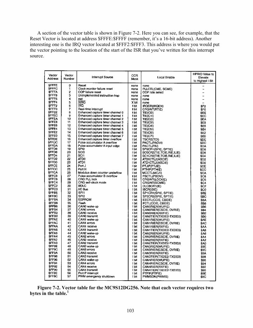
103
A section of the vector table is shown in Figure 7-2. Here you can see, for example, that the Reset Vector is located at address $FFFE:$FFFF (remember, it’s a 16-bit address). Another interesting one is the IRQ vector located at $FFF2:$FFF3. This address is where you would put the vector pointing to the location of the start of the ISR that you’ve written for this interrupt source.
Figure 7-2. Vector table for the MC9S12DG256. Note that each vector requires two
bytes in the table.1

104
What happens when the IRQ pin on the chip is brought low (assuming that the interrupt is not being masked) is that the CPU finishes its current instruction then goes to address $FFF2:$FFF3 to find the vector for that interrupt source. Suppose you’ve put the ISR starting in address $5000. Then the number in address $FFFE:$FFFF should be $5000. The processor loads this number into the Program Counter register, so that the next instruction executed is the first one of your ISR.
By the way, the reason that you bring the IRQ pin low (i.e., to zero) is that it’s actually 𝐼𝑅𝑄. Also note that the “vector” is the number in the address ($5000 in this case), not the table address itself ($FFFE). Finally, as long as we’re talking about the IRQ pin, we should mention that the physical pin itself is connected to Port E, bit 1.
The table also contains some other interesting information, such as whether the interrupt can be masked by a bit in the CCR and whether (and where) an interrupt has a mask in a local register. For example, you can see that the Reset interrupt can’t be masked by the I bit and doesn’t have a local mask. This means it’s a non-maskable interrupt.
In contrast, to unmask the IRQ interrupt you have to clear the I bit and also set a bit in the (local) IRQ Control Register (INTCR) at address $1E. (In the figure it’s labeled IRQCR, but that’s been changed in subsequent versions of CodeWarrior.) The bit that you have to set is bit 6, labeled “IRQEN” for “IRQ Enable.” The default value of the IRQEN bit on startup is 0 (disabled ) for the same reason that the I bit is initially set.
Instant Quiz 1. Find the address of the interrupt vector for the MCCNT Modulus Down Counter. Is it
maskable by the I bit, and does it have a local mask?
2. Repeat question 1 for the swi (software interrupt) instruction.
As an example of how you might use this, suppose that you have a program running that controls an automated drill press, and you would like to add an emergency shutdown switch attached to the IRQ pin. Suppose also that your main code is located in addresses $4000 through $4500 and you want to put your ISR starting at address $5000. Here’s what your code might look like:
org $4000 cli ; this clears the I bit bset INTCR, %01000000 ; set IRQ Enable in the Interrupt Control
; Register forever: ; this is your original program that controls the drill press ; * ; * ; * bra forever
105
org $5000 ; here’s your emergency shutdown ISR ; * ; * ; * rti ; here’s the rti instruction that returns control to ; the main program org $FFF2 dc.w $5000 ; this is the interrupt vector at address $FFF2:$FFF3
Let’s walk through it. The first thing you have to do is to enable the interrupt. You do this in the first two instructions by adding the cli instruction and setting the IRQEN bit (bit 6) in the INTCR register. You can’t put this at the end of your original code because the bra forever instruction will prevent the program from ever getting to it.
Next, the org $5000 directive tells CodeWarrior to put your ISR in address $5000, etc. You end your ISR with an rti instruction.
Finally, you have to load the IRQ vector ($5000) into address $FFF2:$FFF3. You can’t do this with, e.g., a movw instruction because you can’t write to $5000, which is in ROM, during runtime. The org $5000 and the dc.w directives tell CodeWarrior to do this for you when the program is loaded into the microcontroller.
As we’ve seen before, we can just let CodeWarrior figure out where to put the ISR. We can also let CodeWarrior load the correct vector into the table. Here’s the code
org $4000 cli ; this clears the I bit bset INTCR, %01000000 ; set IRQ Enable in the IRQ Control Register
forever: ; this is your original program that controls the drill press ; * ; * ; * bra forever isr: ; here’s your emergency shutdown ISR ; * ; * ; * rti ; here’s the rti instruction that returns control to ; the main program org $FFF2 dc.w isr ; this is the interrupt vector at address $FFF2:$FFF3
106
What we’ve done is to use the label isr to demark the beginning of the interrupt service routine. CodeWarrior will figure out the address of the next line of code (i.e., the first line of the ISR). Then, the line after the org $FFF2 directive will put that address into the correct spot in the vector table. Note that we have to use dc.w because isr represents a 16-bit address.
The XIRQ Interrupt You can clear or set the I bit to enable or disable the IRQ interrupt anywhere and as many
times as you want in your program. The XIRQ works a bit differently. On startup, the X bit in the CCR is set, masking the interrupt. You can clear the X bit in software any time you want but after you do clear it you can’t reset it. That is, the XIRQ interrupt becomes non-maskable until you turn off the microcontroller or hit the Reset button. It is, however, temporarily set when running any other ISR, so that ISR won’t be interrupted by it.
You can clear the X bit using an andcc #%10111111 instruction (AND Condition Code Register).
Periodic Interrupts It’s often useful to be able to generate period interrupts, for example to read a sensor output
or periodically turn on some actuator. An easy way to do this is to use the Modulus down Counter we met in the last chapter. To see how this might work, suppose that every 20 ms we want to produce a 1 ms pulse at Port B bit 0 to trigger a sensor, but we can’t use a simple delay loop because the processor has other tasks to perform. Here’s the code that will do this, assuming a 24 MHz bus clock:
movb #1, DDRB ; Port B bit 0 is output
movb #$c6, MCCTL ; set up MCCNT control register movw #60000, MCCNT ; Down Counter will count down from 60,000 bset MCFLG, $80 cli ; enable interrupts forever: ; put whatever code you want to run normally here
bra forever interruptRoutine: ; this is the interrupt service routine ldy #6000
bset PORTB, 1 ; turn output on
msDelay: ; start ms delay dey bne msDelay bclr PORTB, 1 ; turn off output after ms delay bset MCFLG, $80 ; you have to re-‐clear the MCFLG to repeat

107
rti ; this returns to the main program org $ffca ; this is the location in the vector table for dc.w interruptRoutine ; the Modulus down-‐counter vector
The first two lines set up DDRB and the MCCNT control register; the third loads the number
60,000 into MCCNT; the fourth sets bit 7 of the MCFLG register to clear the flag and start the counting; the fifth enables interrupts by clearing the I bit.
The next lines do whatever you want the microcontroller to be doing when it’s not servicing the interrupt.
The interrupt routine itself is just a simple 1ms delay loop. The thing to note is that you need to re-set the MC Flag each time the ISR runs, otherwise it won’t start counting down again the next time around. Also we used the trick of letting CodeWarrior figure out the value of the interrupt vector.
Instant Quiz
3. In the code above, the number $C6 is loaded into the MCCTL register. Using Figure 6-2 and Table 6-1, figure out the effect of each bit in this number, and, in particular, which bit enables the interrupt, and what is the prescalar value that divides the bus clock.
4. How would you change the code to trigger a sensor every 40 ms?
The WAI Instruction To finish up this chapter on interrupts, we’ll look at one last and very useful instruction, Wait
for Interrupt (wai). When the processor executes this instruction it goes into a wait state in which the CPU stops executing instructions and goes into a power-down mode. This is particularly useful for battery-powered applications. Although the CPU clock is stopped other clocks may still be running so, for example, the timing section is still operating if you’ve enabled any of its timers or counters.
Basically the microcontroller is waiting for any interrupt to occur. When one does, the ISR is executed (including pushing the stack), and then control returns to the main program, popping the stack to restore the system to its original state. It then fetches the instruction immediately after the wai and returns to normal operation.
As a typical application, suppose you want to set up an autonomous, battery-powered intrusion detection system that broadcasts a 1-ms pulse from bit 0 of Port B whenever a motion sensor detects motion. To save power, connect your motion detector to the IRQ pin of you microcontroller (you have to arrange you sensor so that it sends a zero when motion is detected), and then use the following code

108
bset DDRB, 1 ; Port B bit 0 is output movb #%01000000, $1E ; enable IRQ interrupt cli ; enable interrupts forever: ; main program wai ; bra forever ; isr: ; this is the ISR bset 1,1 ; turn bit on
ldy #6000 ; this is the 1 ms delay delay_1ms: ; dey ; bne delay_1ms ; bclr 1,1 ; turn bit off rti ; return to main program, resume waiting org $FFF2 ; IRQ vector = values of isr label dc.w isr
The first lines makes Port B bit 0 an output. The next two lines enable the IRQ interrupt (the
second of the two enables all maskable interrupts). The main program just contains the wai instruction in a continuous loop, so the processor immediately goes into the wait state. It remains in this state until the IRQ interrupt occurs.
When the IRQ interrupt does occur, the processor switches to the ISR, which turns on the bit, waits 1 ms, then turns off the bit. When the ISR is finished, control returns to the instruction in the main program immediately after the wai instruction. This is just the unconditional branch instruction to the forever label, and the instruction after that is wai, so the processor goes right back into the wait state, waiting for the next interrupt. In between intrusion detections the processor clock is disabled, and, since we haven’t turned on any other clocks (TCNT, PWM, etc.) the processor is in a very low power state, drawing just a few microamps from the battery.
Instant Quiz
5. Look up the wai instruction and find its addressing mode(s), the number of clock cycles it takes to execute when the interrupt occurs, and how it affects the CCR bits.

109
Instant Quiz Answers 1. Interrupt vector at $FFCA, maskable by the I bit and a bit in the MCCTL register. (The
actual bit number is bit 7 in Figure 6-2.) 2. Interrupt vector at $FFF6, not maskable by either the I bit or a local bit (it’s a non-
maskable interrupt). 3. $C6 = %11000110, so
Bit 7 = 1; enables the interrupt Bit 6 = 1; the down counter will count down to 0 and repeat
Bit 5 = 0; if you do a read from MCCNT you will get its contents rather than the number with which it is reloaded
Bit 4 = 0; no effect Bit 3 = 0; no effect
Bit 2 = 1; enables (turns on) the counter Bit 1 =1 and bit 0 = 0; from Table 6-1, the prescaler divides by 8
4. Change line 2 to: movb #$c7, MCCTL
5. Addressing mode: INH Access detail: fVfPPP, so 6 bus clock cycles
CCR bits are unaffected
Homework 1. Write a short code fragment to continually read bits 0 and 1 of Port A and turn on bit 0 of
Port B if they are different (feel free to reuse any old code you have, or just write a short lookup table to do this). At the same time, the microcontroller should monitor a sensor attached to the IRQ pin and immediately stop processing and light a warning light at bit 0 of Port J if the bit goes low. You should initially clear the bit in the main program.
2. Write a code fragment to do the following
a) The main program should continuously read the number at PORT A and take an average after each 8 readings. Any time the average is greater than 10, an external alarm attached to Port B bit 0 should be turned on by writing a 1 to the bit. If the average is less than 10 the alarm should be off.
b) At the same time, every 10 ms the processor should momentarily stop what it is doing and read the input from a sensor attached to Port H, bit 0. If this bit is set a warning light attached to bit 1 of Port B should turn on. If the bit is cleared the light should turn off.

110
References 1. Huang, H-W (2010) HCS12/9S12 An Introduction to Software and Hardware Interfacing
(2nd Edition). Clifton Park, NY: Delmar, Cengage Learning.