a clock-tuned digital memristor emulator
TRANSCRIPT

A Clock-Tuned Digital Memristor EmulatorThomas P. Weldon⇤, Patrick J. Kehoe†, and Killian K. Steer†
⇤Department of Electrical and Computer Engineering†Formerly with Dept. of Electrical and Computer Eng.
University of North Carolina at CharlotteCharlotte, NC, USA
Abstract—Memristors are inherently frequency-dependent de-
vices that may be limited by a variety of practical constraints
such as operating frequency ranges of commercially available
devices, or complexity of analog circuit implementations that
emulate memristor behavior. Therefore, a novel clock-tuned
digital memristor emulator is presented, where the frequency-
dependent behavior of the memristor can be tuned over a range
of two decades. An external clock provides simple adjustment of
the operating frequency range and frequency-dependent behavior
of the memristor, without requiring any modification of firmware
or hardware. The digital memristor is implemented in embedded
software on a microcontroller with an integrated analog-to-
digital and digital-to-analog converter, providing a reconfigurable
platform that can support other non-ideal memristor charac-
teristics. Measurements of a prototype demonstrate a clock-
tuned memristor with pinched hysteresis loop v–i curves that
are unchanged over an operating frequency range of 100:1.
I. INTRODUCTION
Memristors have been the subject of intense investigationduring the past few years, due to their potential to transformdiverse applications such as computer memory, data storage,antennas, and neuromorphic computing [1]–[7]. Typically,memristors have a frequency-dependent response with resis-tance determined by a flux or charge, and are characterized bythe presence of a pinched hysteresis loop in the v–i plot and[8]–[11]. Although many investigators have recently focusedon inventing elementary devices such as in [2], others havedeveloped circuits that emulate memristor behavior [12]–[17].Because of limited availability and capability of commercialmemristors, circuits that emulate memristors continue to playan important role in developing new memristor applicationsand in exploring novel types of theoretical memristors.
Since the behavior of memristors is frequency depen-dent [18], it is advantageous to be able to tune a memristorsuch that desired characteristics (such as a particular desiredv–i curve) may occur at some specific frequency for anapplication. Therefore, a novel clock-tuned digital memristoris presented, where the frequency-dependent behavior of thememristor can be tuned over a range of two decades usingan external clock. The proposed memristor is digitally imple-mented using embedded software on an MCU (microcontrollerunit) with an integrated ADC (analog-to-digial converter) andDAC (digital-to-analog converter). Compared to prior digitalmemristor emulators in [14]–[16], the proposed approach pro-vides simple clock tuning without requiring any modificationof firmware or hardware, and does not require a switched-resistor network nor the use of a digital potentiometer. In ad-
dition, clock-tuning may enable adaptively-tuned applications.Lastly, the embedded software should be modifiable to emulateother non-ideal memristors noted in [9].
Section II presents theory for the clock-tuned digital mem-ristor. Section III describes simulations and measured resultsfor a prototype, demonstrating a tuning range of two decades.
II. THEORY
A memristor is a two-terminal device with voltage andcurrent described by a state-dependent Ohm’s law [9]. Thememristance is typically defined by some combination ofvoltage v, current i, electric charge q =
Ri(t) dt, and flux
' =
Rv(t) dt [3]. In this paper, we consider an ideal voltage-
controlled memristor (also referred to as flux-controlled mem-ristor) defined by [11]
i(t) = v(t)G(') = KG
v(t)
'(t)(1)
'(t) = '(0) +
Zt
0v(⌧) d⌧ , (2)
where the memconductance is G(') = KG
/'(t), '(t) is theflux, v(t) is the voltage across the memristor, i(t) is the currentthrough the memristor, and K
G
is a constant scale factor.The block diagram of the proposed clock-tuned memristor
is shown in Fig. 1, where the input digital clock signal “clk”at frequency f
c
= 1/Tc
is used for tuning. The input voltagev(t) is converted to discrete-time signal v[n] = v(nT
c
) bythe ADC, before being digitally processed by the MCU toform v
dac
[n] and DAC output voltage vdac
(t). The memristorcurrent is then i(nT
c
) = i[n] = (v[n]� vdac
[n]) /Rdac
.The flux '(t) from (2) can be approximated for the dig-
ital memristor as '(nTc
) = '[n] ⇡ '[n � 1] + Tc
v[n],where '[0] = '� is the initial flux. Then, G[n] =
Fig. 1. Block diagram of proposed clock-tuned digital memristor, where v(t)is the memristor voltage, i(t) is memristor current, “clk” is the digital clockinput, and where the clock-controlled architecture is similar to [19].

(a) (b) (c)
(d) (e) (f)Fig. 2. Simulated and measured pinched hysteresis loops with 5 kHz clock. Upper three pinched hysteresis loop v–i plots are simulations for 1 V peak inputsine wave at: (a) 10 Hz, (b) 30 Hz, and (c) 90 Hz. Lower three v–i plots are measured data for 1 V peak input sine at: (d) 10 Hz, (e) 30 Hz, and (f) 90 Hz,with 1.5 V dc offset due to unipolar ADC and DAC.
G('[n]) = KG
/'[n], and the input current becomes i[n] =(v[n]� v
dac
[n]) /Rdac
= v[n]KG
/'[n]. Rearranging, thediscrete-time formulation of the proposed memristor in (1)and (2) for Fig. 1 becomes
i[n] = v[n]G(') = KG
v[n]
'[n](3)
'[n] = '� + Tc
nX
↵=1
v[↵] 8 n > 1 (4)
vdac
[n] = v[n]
✓1� R
dac
KG
'[n]
◆(5)
where n � 0, '[0] = '�, and at each step R[n] = 1/G[n] ='[n]/K
G
= v[n]/i[n] is the large-signal chord memristance,as defined in [3].
To provide insight and evaluate results, it is useful tocompute the theoretical current, i
vp
, when the sinusoidalinput voltage is at its peak. A second useful parameter isthe overall peak current, i
p
, during a full cycle of v(t). Toderive these parameters, first let R
min
= R[0] = '�/KG
be the minimum large-signal chord memristance. From theintegral in (2), the peak-to-peak flux for a zero-mean sinusoidalinput v(t) with peak voltage V
p
and signal frequency fs
is'pp
= Vp
/(⇡fs
). The maximum flux is then '� + Vp
/(⇡fs
),leading to a maximum large-signal chord memristance ofR
max
= 1/Gmin
= {'�+Vp
/(⇡fs
)}/KG
. At the time instantof peak voltage for sinusoidal v(t), the integral of half of thepositive cycle of v(t) yields half of the maximum flux change,and thus the theoretical current at the peak input voltage is
ivp
= Vp
/ (Rmin
+ 0.5R�) , (6)
where Rmax
= Rmin
+ R�, and R� = Vp
/(⇡fs
KG
) isthe maximum change in resistance over one cycle. Simi-larly, overall peak current i
p
can by computed by assuming
v(t) = sin(2⇡fs
t) and noting that at t = 0 the flux andlarge-signal chord memristance R(t) are minimum. Then,R(t) must equal R
min
at t = 0, so R(t) = Rmin
+
{1 � cos(2⇡fs
t)}R�/2, and the current must be i(t) =
v(t)/R(t) = 2 sin(2⇡fs
t)/ [2Rmin
+ {1� cos(2⇡fs
t)}R�].Taking the derivative and setting it equal to zero to find themaximum current during a full cycle of v(t) yields
ip
= 2 sin(✓)/[2Rmin
+ {1� cos(✓)}R�] , (7)
where ✓ = cos
�1(R�/{2Rmin
+R�}).Lastly, changes in clock frequency can be best understood
by recalling that (4) is a discrete-time approximation to theintegral in (2) for clock frequency f
c
= 1/Tc
. If the initialexternal clock frequency is f
ca
, and is then changed to adifferent clock frequency f
cb
= 1/Tcb
, the flux becomesimproperly computed as '
b
[n] = '� + Tca
Psin(n2⇡f
sb
Tcb
)
instead of 'b
[n] = '�+Tcb
Psin(n2⇡f
sb
Tcb
). In addition, ifthe initial signal frequency of v(t) is f
sa
, and it is changed toa different signal frequency f
sb
, then the overall peak-to-peakresistance changes from R�a
to R�b
as
R�a
= Vp
/(⇡fsa
KG
) (8)R�b
= fcb
Vp
/(fca
⇡fsb
KG
) , (9)
where it can be observed that R�b
= R�a
if fsa
= fsb
fca
/fcb
or if fsb
= fsa
fcb
/fca
. Therefore, setting a clock frequencyof f
cb
= fsb
fca
/fsa
produces the same memristor behaviorat input frequency f
sb
as was originally obtained for inputfrequency f
sa
with clock fca
. This forms the basis for theproposed clock tuning.
III. SIMULATIONS AND PROTOTYPE MEASUREMENTS
The simulation results in Figs. 2(a)–(c) were generated usingthe relations in (1) and (2) with Mathcad software, for compar-ison to the measured prototype data shown in Figs. 2(d)–(f).

(a) (b) (c)
(d) (e) (f)
Fig. 3. Measured pinched hysteresis loops with clock frequency varied by factor of 100:1. Upper three plots are for a 500 Hz clock and show measuredpinched hysteresis loop v–i plots for 1 V peak input sine wave at: (a) 1 Hz, (b) 3 Hz, and (c) 9 Hz, with 1.5 V dc offset due to unipolar ADC and DAC.Lower three plots are for a 50 kHz clock and show measured v–i plots for 1 V peak input sine wave at: (d) 100 Hz, (e) 300 Hz, and (f) 900 Hz, with 1.5 Vdc offset due to unipolar ADC and DAC. Thus, the operating frequency band shifts by a factor of 100:1.
An NXP FRDM-K64F development board was used to im-plement the prototype of the system of Fig. 1, with embeddedsoftware to compute (3), (4), and (5). Based on the capabilitiesof the FRDM-K64F board with R
dac
= 1000 ohms, the base-line clock frequency of the MCU signal processing softwarewas f
ca
= 1/Tca
= 10 kHz, with KG
= 4 ⇥ 10
�6, and'� = 2⇥ 10
�3, resulting in Rmin
= '�/KG
= 500 ohms.Figs. 2(a)–(c) show simulation results for clock frequency
fc
= 5 kHz, and input sinusoids v(t) of 1 V peak at signalfrequencies f
s
of 10 Hz, 30 Hz, and 90 Hz respectively. Allthree figures show the pinched hysteresis loop v–i character-istic of a memristor [8]. In Fig. 2(a) with f
s
= 10 Hz, R� =
Vp
/(KG
⇡fs
fca
/fc
) = 1/(4 ⇥ 10
�6⇡ · 10 · 10, 000/5, 000) =3979 ohms, resulting in a current when the voltage is peak ofivp
= Vp
/(Rmin
+0.5R�) = 1/(500+0.5·3979) = 0.40 mA,nearly equal to the 0.41 mA from simulation. The predictedoverall maximum current during a full cycle of v(t) yields✓ = cos
�1(R�/{2Rmin
+ R�}) = cos
�1(3979/{2 · 500 +
3979}) = 37
�, and ip
= 2 sin(✓)/[2Rmin
+{1�cos(✓)}R�] =
1.20/1801 = 0.67 mA, equal to the 0.67 mA simulated.Similarly for Fig. 2(b), theoretical R� = 1326 ohms, i
vp
=
0.86 mA compares well with the 0.85 mA simulated, and ✓ =
55
� gives ip
= 1.04 mA nearly equals the 1.05 mA simulated.For Fig. 2(c), theoretical R� = 442 ohms, i
vp
= 1.39 mAcompares well with the 1.38 mA simulated, and ✓ = 72
�
gives ip
= 1.46 mA which equals the 1.46 mA simulated.Figs. 2(d)–(f) show prototype measurement results for clock
frequency fc
= 5 kHz, and input sinusoids v(t) of 1 V peakat signal frequencies f
s
of 10 Hz, 30 Hz, and 90 Hz respec-tively. All three figures closely resemble the correspondingsimulations directly above in Figs. 2(a)–(c), except for a slightasymmetry and left-shifted “pinch point” in Fig. 2(d). As noted
in [9], experimentally-measured pinched hysteresis loops ofsome “real memristors” may not pass through the origin. Inaddition, the voltage axes of the measured data are centeredat 1.5 V instead of 0 V, because the 16-bit ADC and 12-bit DAC of the development board operate between 0 V and3.3 V, requiring the ground reference voltage of the MCUsignal processing to be set at 1.5 V. Nevertheless, bipolarcurrent is possible, since negative current can be producedwhen v(t) < v
dac
(t) in Fig. 1.Next, the frequency tuning of the memristor prototype was
tested for a 100:1 ratio of clock frequencies. Figs. 3(a)–(c) show prototype measurement results for clock frequencyfc
= 500 Hz, and input sinusoids v(t) of 1 V peak at signalfrequencies f
s
of 1 Hz, 3 Hz, and 9 Hz respectively. Figs. 3(d)–(f) show prototype measurement results for clock frequencyfc
= 50 kHz, and input sinusoids v(t) of 1 V peak at signalfrequencies f
s
of 100 Hz, 300 Hz, and 900 Hz respectively.Clearly, the three plots of Figs. 3(a)–(c) at f
c
= 500 Hzclosely resemble the corresponding three plots directly belowin Figs. 3(d)–(f). Thus, the results of Fig. 3 experimentallyconfirm effective tuning of the memristor operating frequencyband over a range of at least two decades, from a memristorsignal frequency band f
s
= 1–9 Hz to fs
= 100–900 Hz. Also,note that Figs. 2(a)–(c) demonstrate the same performanceat an intermediate frequency band of f
s
= 10–90 Hz, forfc
= 5 kHz.Note that for a given clock frequency, the v–i curve is
frequency dependent. For example, when the signal frequencyis changed from 1 Hz in Fig. 3(a) to 9 Hz in Fig. 3(c), thev–i curve changes significantly. Similarly, when the signalfrequency is changed from 100 Hz in Fig. 3(a) to 900 Hz inFig. 3(c), the v–i curve changes significantly. However, note
(a) (b) (c)
(d) (e) (f)
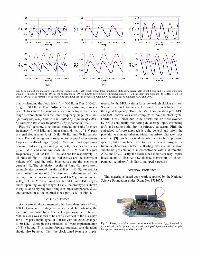
Fig. 4. Simulated and measured time-domain signals with 5 kHz clock. Upper three simulation plots show current i(t) in solid blue and 1 V peak input sinewave v(t) in dotted red at: (a) 10 Hz, (b) 30 Hz, and (c) 90 Hz. Lower three plots are measured data for 1 V peak input sine wave at: (d) 10 Hz, (e) 30 Hz,and (f) 90 Hz, with current i(t) in solid blue and input v(t) in dotted red, with 1.5 V dc offset due to unipolar ADC and DAC.
that by changing the clock from fc
= 500 Hz in Figs. 3(a)–(c),to f
c
= 50 kHz in Figs. 3(d)–(f), the clock-tuning makes itpossible to achieve the same v–i curves in the higher frequencyrange as were obtained in the lower frequency range. Thus, theoperating frequency band can be shifted by a factor of 100:1,by changing the clock frequency f
c
by a factor of 100.Figs. 4(a)–(c) show time-domain simulation results for clock
frequency fc
= 5 kHz, and input sinusoids v(t) of 1 V peakat signal frequencies f
s
of 10 Hz, 30 Hz, and 90 Hz respec-tively. These three figures correspond to the pinched hysteresisloop v–i results of Figs. 2(a)–(c). Measured prototype time-domain results are given in Figs. 4(d)–(f) for clock frequencyfc
= 5 kHz, and input sinusoids v(t) of 1 V peak at signalfrequencies f
s
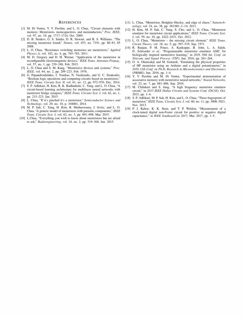
of 10 Hz, 30 Hz, and 90 Hz respectively. Inall plots of Fig. 4, the dotted red curves are the memristorvoltage v(t), and the solid blue curves are the memristorcurrent i(t). The simulation results of Figs. 4(a)–(c) closelyresemble the measured results of Figs. 4(d)–(f), except forthe dc offset voltage of 1.5 V observed in the measured dataarising from the previously mentioned 1.5 V ground referencevoltage of the MCU required for the ADC and DAC single-ended operating voltage ranges. Lastly, the prototype is shownin Fig. 5, and only requires a single external component, R
dac
,and connection to the external clock port “clk” of Fig. 1.
IV. CONCLUSION
A clock-tuned digital memristor has been demonstrated with100:1 change in operating frequency band. In particular, themeasured v–i curve for a 1 V peak input signal at 3 Hz with500 Hz clock was shown to be nearly identical to the v–i curvefor a 1 V peak input signal at 300 Hz with the clock changedto 50 kHz. Although the embedded software implementationof (3), (4), and (5) is straightforward, practical considerationsshould also be noted. First, the clock-tuned feature is imple-
mented by the MCU waiting for a low-to-high clock transition.Second, the clock frequency f
c
should be much higher thanthe signal frequency. Third, the MCU computation plus ADCand DAC conversions must complete within one clock cycle.Fourth, flux ' error due to dc offsets and drift are avoidedby MCU continually monitoring dc average input, correctingdrift, and setting initial flux (in software) at startup. Fifth, theembedded software approach is quite general and offers thepotential to emulate other non-ideal memristor characteristicsnoted in [9]. Such practical details tend to be applicationspecific, but are included here to provide general insights forfuture applications. Further, a floating two-terminal versionshould be possible on a microcontroller with a differentialADC and DAC. Lastly, the clock-tuned memristor may inspireinvestigators to discover new clocked memristors or “clock-pumped memristors” similar to pumped varactors.
ACKNOWLEDGMENT
This material is based upon work supported by the NationalScience Foundation under Grant No. 1731675.
Fig. 5. Prototype of clock-tuned memristor with resistor Rdac installed onterminal strip in foreground, and red wire at top of figure on terminal strip inbackground connecting to clock signal.
REFERENCES
[1] M. Di Ventra, Y. V. Pershin, and L. O. Chua, “Circuit elements withmemory: Memristors, memcapacitors, and meminductors,” Proc. IEEE,vol. 97, no. 10, pp. 1717–1724, Oct. 2009.
[2] D. B. Strukov, G. S. Snider, D. R. Stewart, and R. S. Williams, “Themissing memristor found,” Nature, vol. 453, no. 7191, pp. 80–83, 052008.
[3] L. O. Chua, “Resistance switching memories are memristors,” AppliedPhysics A, vol. 102, no. 4, pp. 765–783, 2011.
[4] M. D. Gregory and D. H. Werner, “Application of the memristor inreconfigurable electromagnetic devices,” IEEE Trans. Antennas Propag.,vol. 57, no. 1, pp. 239–248, Feb. 2015.
[5] L. O. Chua and S. M. Kang, “Memristive devices and systems,” Proc.IEEE, vol. 64, no. 2, pp. 209–223, Feb. 1976.
[6] G. Papandroulidakis, I. Vourkas, N. Vasileiadis, and G. C. Sirakoulis,“Boolean logic operations and computing circuits based on memristors,”IEEE Trans. Circuits Syst. II, vol. 61, no. 12, pp. 972–976, Dec. 2014.
[7] S. P. Adhikari, H. Kim, R. K. Budhathoki, C. Yang, and L. O. Chua, “Acircuit-based learning architecture for multilayer neural networks withmemristor bridge synapses,” IEEE Trans. Circuits Syst. I, vol. 62, no. 1,pp. 215–223, Jan. 2015.
[8] L. Chua, “If it’s pinched it’s a memristor,” Semiconductor Science andTechnology, vol. 29, no. 10, p. 104001, 2014.
[9] M. P. Sah, C. Yang, H. Kim, B. Muthuswamy, J. Jevtic, and L. O.Chua, “A generic model of memristors with parasitic components,” IEEETrans. Circuits Syst. I, vol. 62, no. 3, pp. 891–898, Mar. 2015.
[10] L.Chua, “Everything you wish to know about memristors but are afraidto ask,” Radioengineering, vol. 24, no. 2, pp. 319–368, Jun. 2015.
[11] L. Chua, “Memristor, Hodgkin–Huxley, and edge of chaos,” Nanotech-nology, vol. 24, no. 38, pp. 383 001–1–14, 2013.
[12] H. Kim, M. P. Sah, C. Yang, S. Cho, and L. O. Chua, “Memristoremulator for memristor circuit applications,” IEEE Trans. Circuits Syst.I, vol. 59, no. 10, pp. 2422–2431, Oct. 2012.
[13] L. O. Chua, “Memristor – the missing circuit element,” IEEE Trans.Circuit Theory, vol. 18, no. 5, pp. 507–519, Sep. 1971.
[14] R. Ranjan, P. M. Ponce, A. Kankuppe, B. John, L. A. Saleh,D. Schroeder et al., “Programmable memristor emulator ASIC forbiologically inspired memristive learning,” in 2016 39th Int. Conf. onTelecom. and Signal Process. (TSP), Jun. 2016, pp. 261–264.
[15] O. A. Olumodeji and M. Gottardi, “Emulating the physical propertiesof HP memristor using an Arduino and a digital potentiometer,” in2016 12th Conf. on Ph.D. Research in Microelectronics and Electronics(PRIME), Jun. 2016, pp. 1–4.
[16] Y. V. Pershin and M. Di Ventra, “Experimental demonstration ofassociative memory with memristive neural networks,” Neural Networks,vol. 23, no. 7, pp. 881–886, Sep. 2010.
[17] M. Chilukuri and S. Jung, “A high frequency memristor emulatorcircuit,” in 2015 IEEE Dallas Circuits and Systems Conf. (DCAS), Oct.2015, pp. 1–4.
[18] S. P. Adhikari, M. P. Sah, H. Kim, and L. O. Chua, “Three fingerprints ofmemristor,” IEEE Trans. Circuits Syst. I, vol. 60, no. 11, pp. 3008–3021,Nov. 2013.
[19] P. J. Kehoe, K. K. Steer, and T. P. Weldon, “Measurement of aclock-tuned digital non-Foster circuit for positive or negative digitalcapacitance,” in IEEE SoutheastCon 2017, Mar. 2017, pp. 1–5.