a c om p act xy z s cann er for f ast a tom ic f orce mi ...yy582/papers/yong 2010 - compact...
TRANSCRIPT

A Compact XYZ Scanner for Fast Atomic Force Microscopy in
Constant Force Contact Mode
Yuen Kuan Yong and S. O. Reza Moheimani
Abstract— The design and characterization of a fast flexure-based, parallel-kinematics XYZ scanner for atomic force mi-croscopy is presented in this article. The objective of the projectis to design a AFM scanner with the ability to scan an imageat high-speed and high resolution. Finite-element analysis wasused to optimize the scanner’s design in order to achievehigh resonance frequencies. Experimental results show that thescanner has resonance frequencies of 10kHz at the X, Y and Zaxes. To evaluate the performance of the scanner, it was installedinto a NT-MDT microscope to obtain images. A 3.5µm×3.5µmimage of a calibration grating was successfully recorded upto a scan speed of 625Hz in open-loop. Simulations show thatthe scanner can be operated up to 1025Hz with no oscillationsobserved in the fast axis. The scan rate can be further increasedby means of feedback or feedforward control. The device out-performs commercial AFM scanners that typically work at scanfrequencies below 20-30Hz.
Index Terms— XYZ scanner, fast atomic force microscopy,flexure, finite-element-analysis
I. INTRODUCTION
The Atomic Force Microscope (AFM) is one of the most
versatile tools for imaging at extremely high magnification.
It has resulted in breakthroughs in areas ranging from bio-
nanotechnology [1] to high-density data storage systems [2].
A typical AFM consists of a cantilever with a sharp probe
at one end, a XYZ scanner, a laser and a position sensitive
photodiode (PSD). The laser source in the scanning unit is
focused at the free end of the cantilever and the PSD captures
the laser beam reflected by the cantilever. When operated in
constant force contact mode, the cantilever is slowly brought
into contact with a sample. The probe-sample interaction
causes the cantilever to deflect. This deflection is measured
and compared with the preset deflection value. The scanner,
on which the sample is placed, is then moved in the Z-
direction to reduce the difference between the measured and
preset value by means of vertical feedback controls. After
the cantilever “lands” on the sample, the scanner is actuated
in a zig-zag raster pattern. The vertical feedback controller
is used to maintain the cantilever deflection, therefore main-
taining the probe-sample interaction force during rastering.
A topological image of the sample is constructed from the
electrical signal used to drive the Z-axis of the scanner (see
Fig. 1).
Constant force contact mode AFM has been widely used
to obtain high-resolution images of protein and blood cells
This work was supported by the Australian ResearchCouncils Center of Excellence for Complex Dynamic Systemsand Control. The authors are with the School of ElectricalEngineering and Computer Science, The University of Newcastle,Callaghan 2308, NSW, Australia. [Yuenkuan.Yong,Reza.Moheimani]@newcastle.edu.au
PSD Laser
Cantilever
Probe
XYZ scanner
x
y
z
Sample
Controller
VxVy
Vz
r
Sample profile
Preset
Fig. 1: Schematic of an AFM system in constant force
contact mode. Vx, Vy and Vz are the driven signals. r is
the preset deflection value of the cantilever.
(a)
Z scanner
Z piezo stack
XY
scanner
Sensor
target
Capacitive
sensorBase
Capacitive
sensor
Piezo
stack
Sensor
mounting
hole
(b)
Fig. 2: CAD drawings of the XYZ scanner. (a) Assembly
view. (b) Exploded view.
[1]. The main disadvantage of this mode is its low scan
speed. Conventional AFMs typically take a minute or more
to record a high resolution image [3]. This clearly inadequate
for imaging biological cells that move in milliseconds.
There are many factors limiting the scan speed of an
AFM. These factors include: (i) the resonance frequency of
the cantilever probe [1], (ii) the resonance frequency of the
scanner [4], (iii) the bandwidth of the vertical feedback loop
that controls the probe-sample interaction force [1], [5], and
(iv) the data acquisition system [4].
2010 IEEE/ASME International Conference onAdvanced Intelligent MechatronicsMontréal, Canada, July 6-9, 2010
978-1-4244-8030-2/10/$26.00 ©2010 IEEE 225

Piezoelectric tube scanners are the most widely used
nanopositioning mechanism in commercial AFMs. They
have the lowest resonance frequencies compared to other
AFM components such as cantilever probes. A typical
piezoelectric tube scanner has a first mechanical resonance
frequency of no more than 1kHz. During a raster scan,
a triangular waveform is applied to the fast axis and a
ramp, or staircase, signal is applied to the slow axis. The
triangular waveform contains high-frequency harmonics of
the scan frequency. These high-harmonic components tend
to excite the resonance frequency of the piezoelectric tube
scanner. The low resonant mode of the tube scanner becomes
the bottleneck limitation to the AFM speed. Recently, a
number of commercial AFMs has appeared in the market that
are equipped with flexure-based nanopositioning platforms.
Although, overall these platforms have mechanical properties
superior to tubes, their scan speeds are similarly limited due
to their low first resonance frequencies.
This paper reports the design of a fast parallel-kinematic
AFM scanner for high resolution imaging. The main design
objectives are to increase the scanner resonance frequencies
in X, Y and Z axes and to minimize the cross-coupling effect
among the three scan axes. High-speed serial-kinematic
scanners have been developed for AFM imaging [1], [6].
While these scanners are suitable for raster scans, they
cannot be used for emerging non-raster scan methods, e.g.
[7]. A high-speed parallel-kinematic scanner was presented
in Ref. [4]. The scanner has high resonant modes, but it
contains 9 piezoelectric stack actuators. Each actuator needs
to be driven by a dedicated high voltage amplifier. The
design reported in [4], is thus more expensive and bulkier.
The parallel XYZ scanner presented in this article is much
more compact, consisting of only three piezoelectric stack
actuators.
This article is organized as follows. In Sec. II, the AFM
system and the proposed XYZ scanner are described. A dis-
cussion of design considerations and finite-element-analysis
of the XYZ scanner are presented in Sec. III. Sec. IV presents
the characterization of the scanner by presenting its fre-
quency responses, hysteresis effect and the cross-couplings
associated with its three axes. The imaging capability of the
scanner is presented in Sec. V.
II. THE FAST AFM SCANNER
The proposed AFM scanner consists of a XY nanoposi-
tioner, a Z nanopositioner, a base, three piezoelectric stack
actuators, two capacitive sensors and a sensor target. The
assembly and exploded views of the scanner are shown
in Fig. 2. The scanner is designed to fit into a NT-MDT
NTEGRA scanning probe microscope (SPM) shown in Fig.
3. The XYZ scanner is driven by three external voltage
amplifiers PiezoDrive PDL200. This amplifier has a gain of
20 and selectable maximum output voltages of 60V, 150V
and 200V.
The SPM is configured to operate as an AFM. The AFM’s
software limits the image resolution relative to scanning
speed. At the highest resolution (256×256 scan lines) the
Calibration
grating
Fig. 3: A NT-MDT NTERGA scanning probe microscope
with the original scanner replaced by the flexure-based XYZ
scanner.
fastest achievable scanning frequency is limited to 31Hz.
This limits the performance of the XYZ scanner proposed
in this work. Therefore, a dSPACE-1103 rapid prototyping
system (which has a maximum sampling rate of 80kHz) is
used to generate the X and Y signals and to record the
deflection of the cantilever. The Z signal was controlled
using the AFM’s software and circuitry. With this setup, the
modified AFM can be operated at a scan rate of 625Hz.
III. DESIGN CONSIDERATIONS AND FINITE-ELEMENT
MODELING
A. Flexure-based design
The XYZ scanner has a flexible mechanical structure
where nanoscale motions are generated through elastic de-
formation of flexures [8]. With the absence of moving and
sliding joints, the scanner provides repeatable and smooth
motions without problems such as wear, backlash and fric-
tion. This characteristic is highly desirable for nanoposition-
ing devices.
Each motion axis of the XYZ scanner is driven by a
piezoelectric stack actuator that is capable of providing high
acceleration and large force. For the XY scanner, the central
platform (where the Z scanner is attached) is held by leaf-
spring flexures (see Fig. 4a). The flexures are arranged in
such a way so that they are rigid along the direction of
motion and are flexible in the axis perpendicular to the
motion [9]. As a result, these leaf-spring flexures are used to
guide the motion of each axis, and to simultaneously reduce
the cross-coupling effect from X-to-Y and vice verse. Other
decoupling techniques can be found in Refs. [10], [11].
The Z scanner consists of two identical sets of leaf-
spring flexures located at both sides of the Z scanner. A
piezoelectric stack actuator is located at the middle of the
scanner as shown in Fig. 4b. The leaf-spring flexures are used
to only provide vertical motions along the Z axis. Motions
along other axes are restraint by the flexures.
B. Parallel-kinematic structure
To achieve high-speed scanning, it is required to design
a scanner with high resonance frequencies. The XY and
226
Mounting holes
X and Y
axes piezo
stacksLeaf-spring flexure
(a)
Z-axis
piezo
0
1.5
3
4.5
6 mm
Leaf-spring flexure
(b)
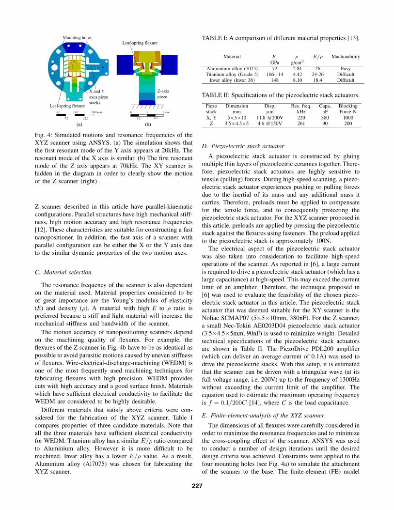
Fig. 4: Simulated motions and resonance frequencies of the
XYZ scanner using ANSYS. (a) The simulation shows that
the first resonant mode of the Y axis appears at 20kHz. The
resonant mode of the X axis is similar. (b) The first resonant
mode of the Z axis appears at 70kHz. The XY scanner is
hidden in the diagram in order to clearly show the motion
of the Z scanner (right) .
Z scanner described in this article have parallel-kinematic
configurations. Parallel structures have high mechanical stiff-
ness, high motion accuracy and high resonance frequencies
[12]. These characteristics are suitable for constructing a fast
nanopositioner. In addition, the fast axis of a scanner with
parallel configuration can be either the X or the Y axis due
to the similar dynamic properties of the two motion axes.
C. Material selection
The resonance frequency of the scanner is also dependent
on the material used. Material properties considered to be
of great importance are the Young’s modulus of elasticity
(E) and density (ρ). A material with high E to ρ ratio is
preferred because a stiff and light material will increase the
mechanical stiffness and bandwidth of the scanner.
The motion accuracy of nanopositioning scanners depend
on the machining quality of flexures. For example, the
flexures of the Z scanner in Fig. 4b have to be as identical as
possible to avoid parasitic motions caused by uneven stiffness
of flexures. Wire-electrical-discharge-machining (WEDM) is
one of the most frequently used machining techniques for
fabricating flexures with high precision. WEDM provides
cuts with high accuracy and a good surface finish. Materials
which have sufficient electrical conductivity to facilitate the
WEDM are considered to be highly desirable.
Different materials that satisfy above criteria were con-
sidered for the fabrication of the XYZ scanner. Table I
compares properties of three candidate materials. Note that
all the three materials have sufficient electrical conductivity
for WEDM. Titanium alloy has a similar E/ρ ratio compared
to Aluminium alloy. However it is more difficult to be
machined. Invar alloy has a lower E/ρ value. As a result,
Aluminium alloy (Al7075) was chosen for fabricating the
XYZ scanner.
TABLE I: A comparison of different material properties [13].
Material E ρ E/ρ Machinability
GPa g/cm3
Aluminium alloy (7075) 72 2.81 26 EasyTitanium alloy (Grade 5) 106-114 4.42 24-26 Difficult
Invar alloy (Invar 36) 148 8.10 18.4 Difficult
TABLE II: Specifications of the piezoelectric stack actuators.
Piezo Dimension Disp. Res. freq. Capa. Blockingstack mm µm kHz nF Force N
X, Y 5×5×10 11.8 @200V 220 380 1000Z 3.5×4.5×5 4.6 @150V 261 90 200
D. Piezoelectric stack actuator
A piezoelectric stack actuator is constructed by gluing
multiple thin layers of piezoelectric ceramics together. There-
fore, piezoelectric stack actuators are highly sensitive to
tensile (pulling) forces. During high-speed scanning, a piezo-
electric stack actuator experiences pushing or pulling forces
due to the inertial of its mass and any additional mass it
carries. Therefore, preloads must be applied to compensate
for the tensile force, and to consequently protecting the
piezoelectric stack actuator. For the XYZ scanner proposed in
this article, preloads are applied by pressing the piezoelectric
stack against the flexures using fasteners. The preload applied
to the piezoelectric stack is approximately 100N.
The electrical aspect of the piezoelectric stack actuator
was also taken into consideration to facilitate high-speed
operations of the scanner. As reported in [6], a large current
is required to drive a piezoelectric stack actuator (which has a
large capacitance) at high-speed. This may exceed the current
limit of an amplifier. Therefore, the technique proposed in
[6] was used to evaluate the feasibility of the chosen piezo-
electric stack actuator in this article. The piezoelectric stack
actuator that was deemed suitable for the XY scanner is the
Noliac SCMAP07 (5×5×10mm, 380nF). For the Z scanner,
a small Nec-Tokin AE0203D04 piezoelectric stack actuator
(3.5×4.5×5mm, 90nF) is used to minimize weight. Detailed
technical specifications of the piezoelectric stack actuators
are shown in Table II. The PiezoDrive PDL200 amplifier
(which can deliver an average current of 0.1A) was used to
drive the piezoelectric stacks. With this setup, it is estimated
that the scanner can be driven with a triangular wave (at its
full voltage range, i.e. 200V) up to the frequency of 1300Hz
without exceeding the current limit of the amplifier. The
equation used to estimate the maximum operating frequency
is f = 0.1/200C [14], where C is the load capacitance.
E. Finite-element-analysis of the XYZ scanner
The dimensions of all flexures were carefully considered in
order to maximize the resonance frequencies and to minimize
the cross-coupling effect of the scanner. ANSYS was used
to conduct a number of design iterations until the desired
design criteria was achieved. Constraints were applied to the
four mounting holes (see Fig. 4a) to simulate the attachment
of the scanner to the base. The finite-element (FE) model
227

102
103
104
−60
−40
−20
0
To
sen
sor
X (
dB
) From input X
102
103
104
−100
−50
0T
o s
enso
r Y
(d
B)
102
103
104
−100
−50
0
To
sen
sor
Z (
dB
)
Frequency (Hz)
102
103
104
−100
−50
0
To
sen
sor
X (
dB
) From input Y
102
103
104
−60
−40
−20
0
To
sen
sor
Y (
dB
)
102
103
104
−100
−50
0
To
sen
sor
Z (
dB
)
Frequency (Hz)
102
103
104
−100
−50
0
To
sen
sor
X (
dB
) From input Z
102
103
104
−100
−50
0
To
sen
sor
Y (
dB
)
102
103
104
−60
−40
−20
0
Frequency (Hz)
To
sen
sor
Z (
dB
)
Fig. 5: Frequency responses of the XYZ scanner.
of the scanner are shown in Fig. 4. The first resonant mode
of both the X and Y axes appears at 20kHz, while the first
resonant mode of the Z axis appears at 70kHz.
IV. CHARACTERIZATION OF THE XYZ SCANNER
A. Measured frequency responses
The frequency responses of the scanner were obtained
using a HP 35670A dual channel spectrum analyzer. A
swept sine input of 100mVpk, with the frequency range
of 100Hz to 20kHz, was applied to the piezoelectric stack
amplifier. The scanner output displacements were measured
using capacitive sensors (in volts). The frequency responses
of the scanner are plotted in Fig. 5. The first resonance
frequency appears at 10kHz in the X, Y and Z axes, which
is different from the FE modeling results. An investigation
was carried out to study the differences. It was revealed that
the 10kHz resonant mode is attributed to the base of the
scanner which was not simulated in the FE model. A new
FE model taking into account the effect of the base was
constructed. Simulations show that the two sensor mounting
holes at the side of the base (see Fig. 2b) soften the structure,
which in turn reduces the resonance frequency of the base
significantly. The base design needs further considerations.
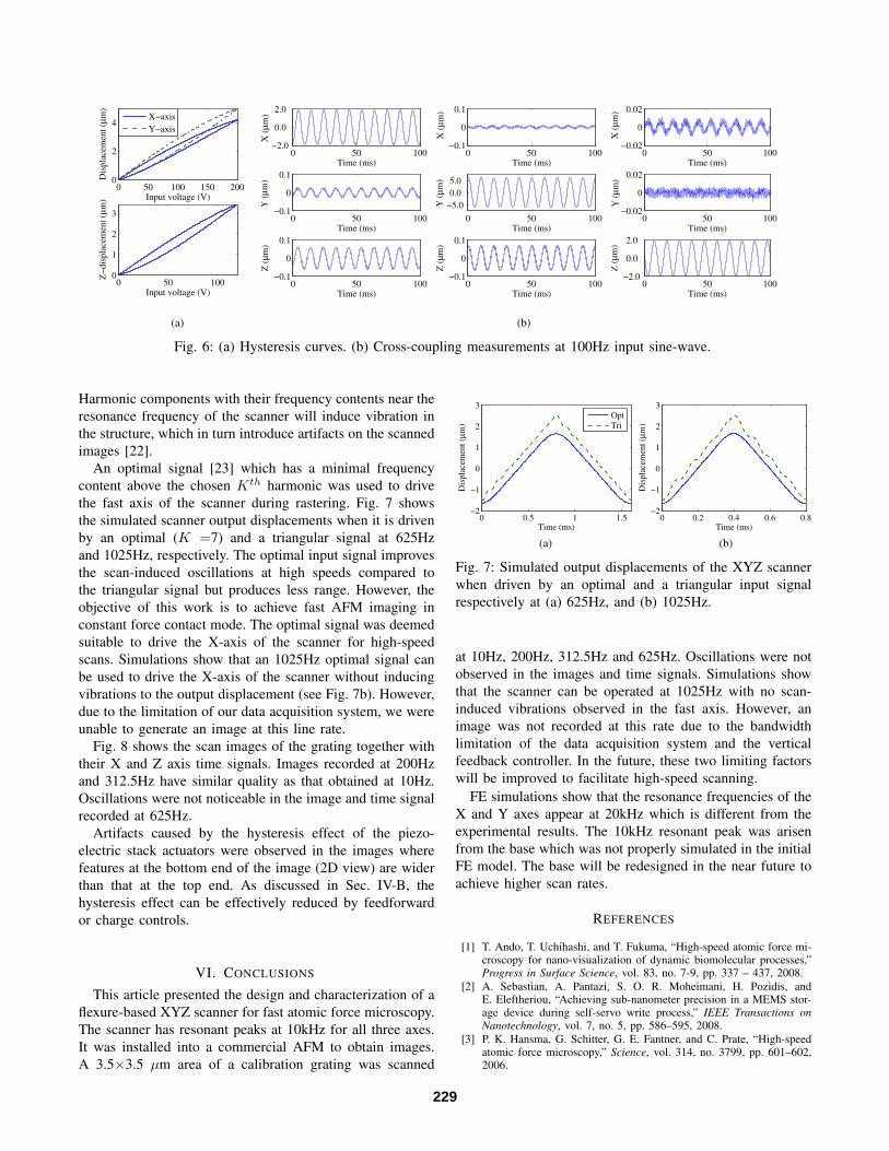
B. Hysteresis and cross-coupling measurements
The hysteretic behavior of piezoelectric stack actuators
will often cause artifacts in an open-loop AFM scan. This
artifact can be found in the AFM images reported in Sec.
V. It is important to characterize the hysteresis effect asso-
ciated with a scanner, so that a method may be applied to
compensate for the hysteresis.
To identify the hysteresis loop, a 100Hz triangular wave-
form was applied to the X, Y and Z axes respectively.
A voltage range of 0-200V was applied to the X and Y
axes, while 0-120V was applied to the Z axis. Table III
documents the maximum width of the hysteresis loop and
its percentage over the displacement range of each axis. The
hysteresis effect can be compensated using techniques such
as feedforward control [15], [16]. Accurate hysteresis models
such as Preisach model [17] and Prandtl-Ishlinskii operator
TABLE III: Measured hysteresis curves.
Max. width (µm) Disp. range (µm) %
X 0.6 4.2 14Y 0.8 5.0 16Z 0.5 3.4 15
[18] can be used in conjunction with feedforward techniques
to minimize the hysteresis effect. Besides, charge amplifiers
can also be used to linearize piezoelectric stack actuators [8],
[19].
The cross-coupling effect among the three axes has been
one of the complications that affects the quality of AFM im-
ages [20]. Fig. 6 plots the measured cross-coupling motions
of the scanner. When a 200V peak-to-peak sine-wave was
applied to the X axis, the induced Y and Z displacements
were 1.58% and 3.4% of the X displacement respectively.
By applying the sine-wave to the Y axis, it induces 0.5%
and 2.9% in the X and Z displacements respectively. When
the Z axis is being driven, it induces 0.61% in the X
displacement and 0.45% in the Y displacement. The effect of
these cross-coupling motions on AFM images can be reduced
by implementing feedback control techniques [11], [20] or
by post-processing image data offline [21].
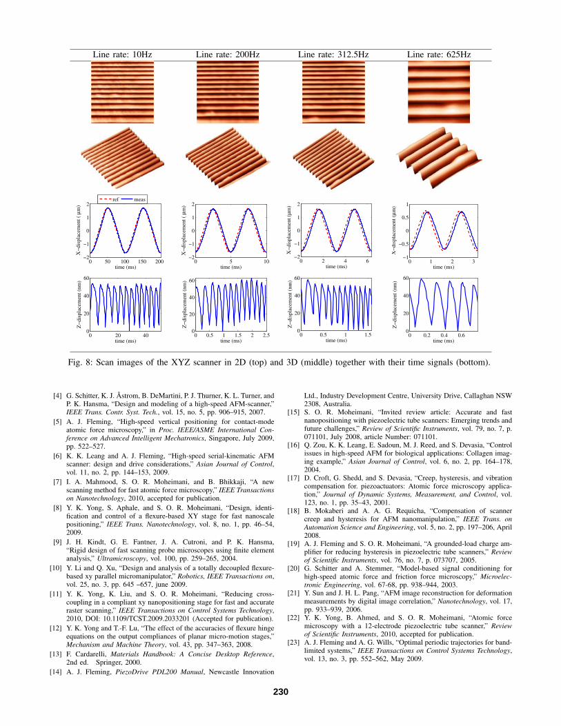
V. ATOMIC FORCE MICROSCOPY IMAGING
The scanner was installed in the AFM to obtain images of
a MikroMasch TDG01 calibration grating. The grating has
parallel ridges with 278nm period and approximately 55nm
height. 3.5µm×3.5µm images of the grating were recorded
in constant force contact mode at 10Hz (256×256 lines),
200Hz (200×200 lines) and 312.5Hz (128×128 lines). Due
to the bandwidth limitation of the data acquisition system,
the scan lines had to be reduced as the scan rate increases.
To obtain an image with an acceptable resolution at 625Hz
(64×64 lines), the size of the image had to be reduced to
1.5µm×1.5µm.
During a typical raster scan, a triangular waveform is
applied to the fast axis and a staircase, or ramp, signal is
applied to the slow axis. However, the triangular waveform
contains all odd harmonics of the fundamental frequency.
228
0 50 100 150 2000
2
4
Input voltage (V)
Dis
pla
cem
ent
(µm
)
0 50 1000
1
2
3
Input voltage (V)
Z−
dis
pla
cem
ent
(µm
)
X−axis
Y−axis
(a)
0 50 100−2.0
0.0
2.0
Time (ms)
X (
µm
)
0 50 100−0.1
0
0.1
Time (ms)
Y (
µm
)
0 50 100−0.1
0
0.1
Time (ms)
Z (
µm
)
0 50 100−0.1
0
0.1
Time (ms)
X (
µm
)
0 50 100
−5.0
0.0
5.0
Time (ms)
Y (
µm
)
0 50 100−0.1
0
0.1
Time (ms)
Z (
µm
)
0 50 100−0.02
0
0.02
Time (ms)
X (
µm
)
0 50 100−0.02
0
0.02
Time (ms)
Y (
µm
)
0 50 100−2.0
0.0
2.0
Time (ms)
Z (
µm
)
(b)
Fig. 6: (a) Hysteresis curves. (b) Cross-coupling measurements at 100Hz input sine-wave.
Harmonic components with their frequency contents near the
resonance frequency of the scanner will induce vibration in
the structure, which in turn introduce artifacts on the scanned
images [22].
An optimal signal [23] which has a minimal frequency
content above the chosen Kth harmonic was used to drive
the fast axis of the scanner during rastering. Fig. 7 shows
the simulated scanner output displacements when it is driven
by an optimal (K =7) and a triangular signal at 625Hz
and 1025Hz, respectively. The optimal input signal improves
the scan-induced oscillations at high speeds compared to
the triangular signal but produces less range. However, the
objective of this work is to achieve fast AFM imaging in
constant force contact mode. The optimal signal was deemed
suitable to drive the X-axis of the scanner for high-speed
scans. Simulations show that an 1025Hz optimal signal can
be used to drive the X-axis of the scanner without inducing
vibrations to the output displacement (see Fig. 7b). However,
due to the limitation of our data acquisition system, we were
unable to generate an image at this line rate.
Fig. 8 shows the scan images of the grating together with
their X and Z axis time signals. Images recorded at 200Hz
and 312.5Hz have similar quality as that obtained at 10Hz.
Oscillations were not noticeable in the image and time signal
recorded at 625Hz.
Artifacts caused by the hysteresis effect of the piezo-
electric stack actuators were observed in the images where
features at the bottom end of the image (2D view) are wider
than that at the top end. As discussed in Sec. IV-B, the
hysteresis effect can be effectively reduced by feedforward
or charge controls.
VI. CONCLUSIONS
This article presented the design and characterization of a
flexure-based XYZ scanner for fast atomic force microscopy.
The scanner has resonant peaks at 10kHz for all three axes.
It was installed into a commercial AFM to obtain images.
A 3.5×3.5 µm area of a calibration grating was scanned
0 0.5 1 1.5−2
−1
0
1
2
3
Dis
pla
cem
ent
(µm
)
Time (ms)
Opt
Tri
(a)
0 0.2 0.4 0.6 0.8−2
−1
0
1
2
3
Dis
pla
cem
ent
(µm
)
Time (ms)
(b)
Fig. 7: Simulated output displacements of the XYZ scanner
when driven by an optimal and a triangular input signal
respectively at (a) 625Hz, and (b) 1025Hz.
at 10Hz, 200Hz, 312.5Hz and 625Hz. Oscillations were not
observed in the images and time signals. Simulations show
that the scanner can be operated at 1025Hz with no scan-
induced vibrations observed in the fast axis. However, an
image was not recorded at this rate due to the bandwidth
limitation of the data acquisition system and the vertical
feedback controller. In the future, these two limiting factors
will be improved to facilitate high-speed scanning.
FE simulations show that the resonance frequencies of the
X and Y axes appear at 20kHz which is different from the
experimental results. The 10kHz resonant peak was arisen
from the base which was not properly simulated in the initial
FE model. The base will be redesigned in the near future to
achieve higher scan rates.
REFERENCES
[1] T. Ando, T. Uchihashi, and T. Fukuma, “High-speed atomic force mi-croscopy for nano-visualization of dynamic biomolecular processes,”Progress in Surface Science, vol. 83, no. 7-9, pp. 337 – 437, 2008.
[2] A. Sebastian, A. Pantazi, S. O. R. Moheimani, H. Pozidis, andE. Eleftheriou, “Achieving sub-nanometer precision in a MEMS stor-age device during self-servo write process,” IEEE Transactions on
Nanotechnology, vol. 7, no. 5, pp. 586–595, 2008.
[3] P. K. Hansma, G. Schitter, G. E. Fantner, and C. Prate, “High-speedatomic force microscopy,” Science, vol. 314, no. 3799, pp. 601–602,2006.
229
Line rate: 10Hz Line rate: 200Hz Line rate: 312.5Hz Line rate: 625Hz
0 50 100 150 200−2
−1
0
1
2
time (ms)
X−
dis
pla
cem
ent
( µ
m)
ref meas
0 20 400
20
40
60
time (ms)
Z−
dis
pla
cem
ent
(nm
)
0 5 10−2
−1
0
1
2
time (ms)
X−
dis
pla
cem
ent
( µ
m)
0 0.5 1 1.5 2 2.50
20
40
60
time (ms)
Z−
dis
pla
cem
ent
(nm
)
0 2 4 6−2
−1
0
1
2
time (ms)
X−
dis
pla
cem
ent
(µm
)
0 0.5 1 1.50
20
40
60
time (ms)
Z−
dis
pla
cem
ent
(nm
)
0 1 2 3−1
−0.5
0
0.5
1
time (ms)
X−
dis
pla
cem
ent
(µm
)
0 0.2 0.4 0.60
20
40
60
time (ms)
Z−
dis
pla
cem
ent
(nm
)
Fig. 8: Scan images of the XYZ scanner in 2D (top) and 3D (middle) together with their time signals (bottom).
[4] G. Schitter, K. J. Astrom, B. DeMartini, P. J. Thurner, K. L. Turner, andP. K. Hansma, “Design and modeling of a high-speed AFM-scanner,”IEEE Trans. Contr. Syst. Tech., vol. 15, no. 5, pp. 906–915, 2007.
[5] A. J. Fleming, “High-speed vertical positioning for contact-modeatomic force microscopy,” in Proc. IEEE/ASME International Con-
ference on Advanced Intelligent Mechatronics, Singapore, July 2009,pp. 522–527.
[6] K. K. Leang and A. J. Fleming, “High-speed serial-kinematic AFMscanner: design and drive considerations,” Asian Journal of Control,vol. 11, no. 2, pp. 144–153, 2009.
[7] I. A. Mahmood, S. O. R. Moheimani, and B. Bhikkaji, “A newscanning method for fast atomic force microscopy,” IEEE Transactions
on Nanotechnology, 2010, accepted for publication.
[8] Y. K. Yong, S. Aphale, and S. O. R. Moheimani, “Design, identi-fication and control of a flexure-based XY stage for fast nanoscalepositioning,” IEEE Trans. Nanotechnology, vol. 8, no. 1, pp. 46–54,2009.
[9] J. H. Kindt, G. E. Fantner, J. A. Cutroni, and P. K. Hansma,“Rigid design of fast scanning probe microscopes using finite elementanalysis,” Ultramicroscopy, vol. 100, pp. 259–265, 2004.
[10] Y. Li and Q. Xu, “Design and analysis of a totally decoupled flexure-based xy parallel micromanipulator,” Robotics, IEEE Transactions on,vol. 25, no. 3, pp. 645 –657, june 2009.
[11] Y. K. Yong, K. Liu, and S. O. R. Moheimani, “Reducing cross-coupling in a compliant xy nanopositioning stage for fast and accurateraster scanning,” IEEE Transactions on Control Systems Technology,2010, DOI: 10.1109/TCST.2009.2033201 (Accepted for publication).
[12] Y. K. Yong and T.-F. Lu, “The effect of the accuracies of flexure hingeequations on the output compliances of planar micro-motion stages,”Mechanism and Machine Theory, vol. 43, pp. 347–363, 2008.
[13] F. Cardarelli, Materials Handbook: A Concise Desktop Reference,2nd ed. Springer, 2000.
[14] A. J. Fleming, PiezoDrive PDL200 Manual, Newcastle Innovation
Ltd., Industry Development Centre, University Drive, Callaghan NSW2308, Australia.
[15] S. O. R. Moheimani, “Invited review article: Accurate and fastnanopositioning with piezoelectric tube scanners: Emerging trends andfuture challenges,” Review of Scientific Instruments, vol. 79, no. 7, p.071101, July 2008, article Number: 071101.
[16] Q. Zou, K. K. Leang, E. Sadoun, M. J. Reed, and S. Devasia, “Controlissues in high-speed AFM for biological applications: Collagen imag-ing example,” Asian Journal of Control, vol. 6, no. 2, pp. 164–178,2004.
[17] D. Croft, G. Shedd, and S. Devasia, “Creep, hysteresis, and vibrationcompensation for. piezoactuators: Atomic force microscopy applica-tion,” Journal of Dynamic Systems, Measurement, and Control, vol.123, no. 1, pp. 35–43, 2001.
[18] B. Mokaberi and A. A. G. Requicha, “Compensation of scannercreep and hysteresis for AFM nanomanipulation,” IEEE Trans. on
Automation Science and Engineering, vol. 5, no. 2, pp. 197–206, April2008.
[19] A. J. Fleming and S. O. R. Moheimani, “A grounded-load charge am-plifier for reducing hysteresis in piezoelectric tube scanners,” Review
of Scientific Instruments, vol. 76, no. 7, p. 073707, 2005.[20] G. Schitter and A. Stemmer, “Model-based signal conditioning for
high-speed atomic force and friction force microscopy,” Microelec-
tronic Engineering, vol. 67-68, pp. 938–944, 2003.[21] Y. Sun and J. H. L. Pang, “AFM image reconstruction for deformation
measurements by digital image correlation,” Nanotechnology, vol. 17,pp. 933–939, 2006.
[22] Y. K. Yong, B. Ahmed, and S. O. R. Moheimani, “Atomic forcemicroscopy with a 12-electrode piezoelectric tube scanner,” Review
of Scientific Instruments, 2010, accepted for publication.[23] A. J. Fleming and A. G. Wills, “Optimal periodic trajectories for band-
limited systems,” IEEE Transactions on Control Systems Technology,vol. 13, no. 3, pp. 552–562, May 2009.
230