a better approach to dc power filtering - jastech … better approach to dc... · a better approach...
TRANSCRIPT

A Better Approach to DC Power Filtering Dale L. Sanders James P. Muccioli Anthony A. Anthony
X2Y Attenuators, LLC 37554 Hills Tech Dr.
Farmington Hills, MI 48331 [email protected]
X2Y Attenuators, LLC 37554 Hills Tech Dr.
Farmington Hills, MI 48331 [email protected]
X2Y Attenuators, LLC 2730 West 21st Street Erie, PA 16506-2972
Abstract—The goal of DC power filtering is to provide stable DC power and reduce electromagnetic interference (EMI) and transients. As integrated circuits (IC) on printed circuit boards (PCB) increase in power demands, have faster switching frequencies and larger population densities, power filtering gains in cost, complexity, and frequency range. The purpose of this paper is to highlight the radiated emissions results of a microprocessor development board using different combinations and configurations of power filters and evaluating it against the X2Y® Technology.
Keywords-X2Y®; X2Y® Technology; filtering; Radiated Emissions; cancellation; passive component;
I. INTRODUCTION X2Y® Technology is the newest approach in passive
component technology for filtering. Traditional passive components use brute force (shunting and/or blocking) to remove unwanted common mode or differential mode noise. The X2Y® Technology differs from this in that the unique structure is utilized for broadband E- and H-field cancellation of noise. The structure promotes the cancellation of mutual inductance internally which in turn provides a low-impedance for noise. The structure is similar to a traditional bypass capacitor structure with separately terminated ‘A’ and ‘B’ electrode layers. The difference is additional terminated reference (ground) electrode layers (the terminations are ‘G1’ and ‘G2’) are inserted between the ‘A’ and ‘B’ electrodes in parallel forming a quasi Faraday Cage (Fig. 1) [1]. The result is a 4-terminal device that comes in standard MLCC package sizes, 0603, 0805, 1206, 1210, 1410, 1812, and 2220.
Figure 1. Depiction of X2Y® structure.
The connection configuration of the X2Y® component to a circuit can have several different orientations, thus modes of operation, with respect to the source and load. Changing the orientation utilizes structure in different ways. Thus, X2Y®
components are viewed as symmetrically balanced capacitive circuits not simply as a discrete passive device [2]. It should be noted that the X2Y® chip components are applied to circuits in bypass and therefore should not be confused as a chip feedthrough capacitor.
For the purposes of this paper, the connection configuration utilized will be Circuit 1. (The Circuit 1 configuration has been defined by the inventor and manufacturers of X2Y® Technology [2].) Circuit 1 is a differential circuit application that utilizes three independent conductor connections to the structure. For the purposes of this paper the conductors are: (+) power, (-) power, and ground (Fig. 2).
Figure 2. Circuit 1 schematic.
The capacitive rating of X2Y® components is a Line-to-ground measurement which divides the structure into two capacitive halves. For example, an X2Y® component with a 100nF capacitive rating has 100nF of capacitance between the ‘A’ terminal and the ‘G1’/‘G2’ terminals and 100nF of capacitance between the ‘B’ terminal and the ‘G1’/‘G2’ terminals (Cy in Fig. 3). Therefore, the total capacitance supplied between the ‘A’ and ‘B’ terminal as seen in a series-thru measurement (Circuit 1) with respect to the load is 50nF or ½ the capacitive rating (Cx in Fig. 3). Unsorted X2Y® components have a variance of 2.5% or less in X7R dielectric between the capacitive halves due to the shared electrodes and dielectric; which additionally allows capacitive tolerance to be maintained over temperature and time (aging).
Figure 3. Illistration of X2Y® capacitive rating.
0-7803-8444-X/04/$20.00 (C) IEEE

II. TEST PROTOCOL The experiment will consist of placing a programmed
single board computer (CMD-11E1 manufactured by Axiom Manufacturing, INC.) into a 3.25 inch radius metal enclosure. The (+) and (-) power leads are extended through the side of the enclosure (Fig. 4).
Figure 4. Single computer board and metal enclosure.
The metal enclosure and DC power supply will then be placed into a GTEM (ETS-Lindgren IC-GTEM 250) with a 3 meter power harness between the metal enclosure and power supply (Fig. 5). Radiated emissions will be recorded with a spectrum analyzer (IFR AN920). When necessary, an external 30dB preamp (AR LN1000) will be used (Fig. 6).
Figure 5. GTEM (ETS-Lindgren IC-GTEM 250).
Figure 6. Spectrum Analyzer (IFR AN920) & preamp (ARLN1000).
The experiment will evaluate the following four types of filters:
Ferrite Bead
Pi filter
(1) MLCC connected Line-to-Ground on both the (+) and (-) power leads - (2) Y-caps
(1) MLCC connected Line-to-Ground on both (+) and (-) power leads and (1) MLCC connected between (+) and (-) power leads – X & (2) Y-caps
and compare their performance against the X2Y® Chip Technology.
The analysis of each filter and the comparison to the X2Y® Technology on an individual basis were done at the same time,
with the same equipment, and same test methodology. However, individual analysis included in this paper spans several months. Efforts were made to repeat protocol exactly between individual analyses, but two factors prevented better cross-correlation results:
1) Equipment was recalibrated in-between individual filter analyses and comparison.
2) The length of the (+) and (-) power leads coming out of the metal enclosure varied (maximum of 3 inches).
The spectrum analyzer was used to sweep two frequency ranges, 100kHz – 200MHz (which was used in conjunction with the 30dB pre-amp) and 200MHz – 1GHz. For each frequency range three sweeps were used recording the largest peak values. TABLE 1 lists the analyzer’s set-up configuration.
TABLE I. SPECTRUM ANALYZER SET-UP.
Frequency Range: 100kHz - 200MHz 200MHz - 1GHz Sweep: 8 x 5 ms 8 x10 ms Bandwidth: 120 Khz 120 Khz Video: none none Atten: 20 dB 0 dB Internal Gain: 0 dB 0 dB Measurement: dBuV dBuV External Preamp: 30 dB none
The location and mounting of the X2Y® Technology for all measurements unless otherwise noted is on a small PCB mounted on the exterior of the metal enclosure.
Figure 7. Picture of X2Y® set-up on metal enclosure.
III. ANALYSIS – FERRITE BEAD VS. X2Y® The ferrite beads are placed around both the (+) and (-)
power leads exiting the metal enclosure (Fig. 8). Two different beads were tested. TABLE II shows the bead’s impedances at 25MHz and 100MHz. The X2Y® Technology used for comparison is an X2Y® 1206 (0.1uF). Fig. 9 and Fig. 10 show the measured radiated results of the ferrite beads and the X2Y® Technology.
TABLE II. FERRITE BEAD IMPEDANCES.
Z @ 25MHz (ohms) Z @ 100MHz (ohms) Bead A 160 258 Bead B 66 110
0-7803-8444-X/04/$20.00 (C) IEEE
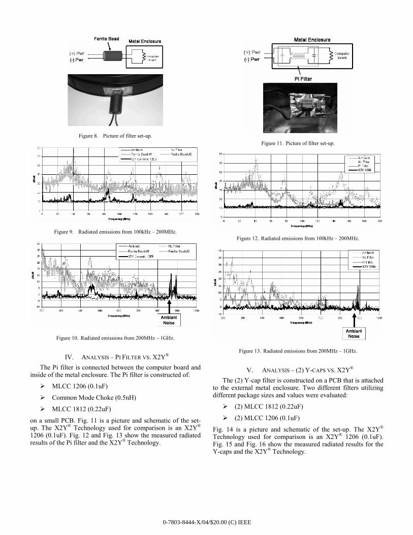
Figure 8. Picture of filter set-up.
Figure 9. Radiated emissions from 100kHz – 200MHz.
Figure 10. Radiated emissions from 200MHz – 1GHz.
IV. ANALYSIS – PI FILTER VS. X2Y® The Pi filter is connected between the computer board and
inside of the metal enclosure. The Pi filter is constructed of:
MLCC 1206 (0.1uF)
Common Mode Choke (0.5nH)
MLCC 1812 (0.22uF)
on a small PCB. Fig. 11 is a picture and schematic of the set-up. The X2Y® Technology used for comparison is an X2Y® 1206 (0.1uF). Fig. 12 and Fig. 13 show the measured radiated results of the Pi filter and the X2Y® Technology.
Figure 11. Picture of filter set-up.
Figure 12. Radiated emissions from 100kHz – 200MHz.
Figure 13. Radiated emissions from 200MHz – 1GHz.
V. ANALYSIS – (2) Y-CAPS VS. X2Y® The (2) Y-cap filter is constructed on a PCB that is attached
to the external metal enclosure. Two different filters utilizing different package sizes and values were evaluated:
(2) MLCC 1812 (0.22uF)
(2) MLCC 1206 (0.1uF)
Fig. 14 is a picture and schematic of the set-up. The X2Y® Technology used for comparison is an X2Y® 1206 (0.1uF). Fig. 15 and Fig. 16 show the measured radiated results for the Y-caps and the X2Y® Technology.
0-7803-8444-X/04/$20.00 (C) IEEE

Figure 14. Picture of filter set-up.
Figure 15. Radiated emissions from 100kHz – 200MHz.
Figure 16. Radiated emissions from 200MHz – 1GHz.
VI. ANALYSIS – X & (2) Y-CAPS VS. X2Y® The X- and (2) Y-cap filter is constructed on a PCB that is
attached to the external metal enclosure. Two different filters utilizing different package sizes and values were evaluated:
Y-caps = 1812 (0.22uF); X-cap = 1812 (0.12uF)
Y-caps = 1206 (0.1uF); X-cap = 1206 (0.47uF)
Fig. 17 is a picture and schematic of the set-up. The X2Y® Technology used for comparison is an X2Y® 1206 (0.1uF). Fig. 18 and Fig. 19 show the measured radiated results of the X & (2) Y-caps and the X2Y® Technology.
Figure 17. Picture of filter set-up.
Figure 18. Radiated emissions from 100kHz – 200MHz.
Figure 19. Radiated emissions from 200MHz – 1GHz.
VII. ANALYSIS – FURTHER EVALUATION OF X2Y® TECHNOLOGY
This section investigates the performance of the X2Y® Technology with alternative locations (inside vs. outside metal enclosure) and the effect if (-) power and chassis ground are the same.
A. X2Y® located inside vs. outside metal enclosure. Small PCBs were attached to the inside and outside of the
metal enclosure where the power leads go through. A 1206 (0.1uF) X2Y® was tested at each position. Fig.20 is a picture of each location and Fig. 21 and Fig. 22 are the measured radiated results.
0-7803-8444-X/04/$20.00 (C) IEEE

Figure 20. Picture of filter set-up.
Figure 21. Radiated emissions from 100kHz – 200MHz.
Figure 22. Radiated emissions from 200MHz – 1GHz.
B. (-) power (Return) is also attached to Chassis Ground. Using the internal PCB, a 1206 (0.1uF) X2Y® is attached
and the (-) power lead is soldered to the inside metal enclosure. Fig.23 is a schematic and picture of the set-up. Fig. 24 and Fig. 25 are the measured radiated results comparing (-) power attached to the metal enclosure and when it is independent of the enclosure.
Figure 23. Picture of filter set-up.
Figure 24. Radiated emissions from 100kHz – 200MHz.
Figure 25. Radiated emissions from 200MHz – 1GHz.
VIII. CONCLUSIONS The X2Y® Technology showed significant improvement in
reducing the radiated emissions when compared to four typical filter configurations. In addition, three variations of the Circuit 1 configuration give circuit designers flexibility in implementation while still providing broadband performance. When considering placement cost and component reduction, the X2Y® Technology has been shown to provide cost savings as well as a performance improvement.
ACKNOWLEDGMENTS We would like to thank Dave Anthony, Ken Musil, Mary Haldi, and William Anthony for their comments and time.
REFERENCES [1] “Internal Model of X2Y,” Application Note # 1004,
http://www.x2y.com/cube/x2y.nsf/(files)/InternalModel090203.pdf/$FILE/InternalModel090203.pdf.
[2] “X2Y® Circuit 1 & Circuit 2 Configuration,” Application Note # 1006, http://www.x2y.com/cube/x2y.nsf/(files)/CircuitConfig112703.pdf/$FILE/CircuitConfig112703.pdf
0-7803-8444-X/04/$20.00 (C) IEEE