a 500 ksps, differential adc 16-bit, 1 lsb inl, ad7676
TRANSCRIPT
REV. B
Information furnished by Analog Devices is believed to be accurate andreliable. However, no responsibility is assumed by Analog Devices for itsuse, nor for any infringements of patents or other rights of third parties thatmay result from its use. No license is granted by implication or otherwiseunder any patent or patent rights of Analog Devices.
aAD7676
One Technology Way, P.O. Box 9106, Norwood, MA 02062-9106, U.S.A.
Tel: 781/329-4700 www.analog.com
Fax: 781/326-8703 © Analog Devices, Inc., 2002
16-Bit, 1 LSB INL,500 kSPS, Differential ADC
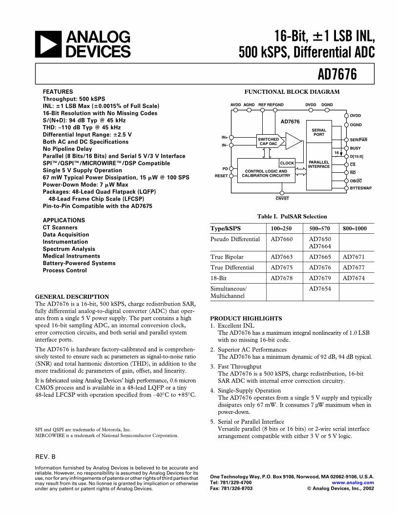
FUNCTIONAL BLOCK DIAGRAM
CONTROL LOGIC ANDCALIBRATION CIRCUITRY
CLOCK
OB/2C
16D[15:0]
BUSY
CS
SER/PAR
OGND
OVDD
DGNDDVDD
SERIALPORT
PARALLELINTERFACE
BYTESWAP
RD
AVDD AGND REF REFGND
PD
RESET
CNVST
IN–SWITCHEDCAP DAC
AD7676
IN+
Table I. PulSAR Selection
Type/kSPS 100–250 500–570 800–1000
Pseudo Differential AD7660 AD7650AD7664
True Bipolar AD7663 AD7665 AD7671
True Differential AD7675 AD7676 AD7677
18-Bit AD7678 AD7679 AD7674
Simultaneous/ AD7654Multichannel
FEATURES
Throughput: 500 kSPS
INL: 1 LSB Max (0.0015% of Full Scale)
16-Bit Resolution with No Missing Codes
S/(N+D): 94 dB Typ @ 45 kHz
THD: –110 dB Typ @ 45 kHz
Differential Input Range: 2.5 V
Both AC and DC Specifications
No Pipeline Delay
Parallel (8 Bits/16 Bits) and Serial 5 V/3 V Interface
SPI™/QSPI™/MICROWIRE™/DSP Compatible
Single 5 V Supply Operation
67 mW Typical Power Dissipation, 15 W @ 100 SPS
Power-Down Mode: 7 W Max
Packages: 48-Lead Quad Flatpack (LQFP)
48-Lead Frame Chip Scale (LFCSP)
Pin-to-Pin Compatible with the AD7675
APPLICATIONS
CT Scanners
Data Acquisition
Instrumentation
Spectrum Analysis
Medical Instruments
Battery-Powered Systems
Process Control
GENERAL DESCRIPTIONThe AD7676 is a 16-bit, 500 kSPS, charge redistribution SAR,fully differential analog-to-digital converter (ADC) that oper-ates from a single 5 V power supply. The part contains a highspeed 16-bit sampling ADC, an internal conversion clock,error correction circuits, and both serial and parallel systeminterface ports.
The AD7676 is hardware factory-calibrated and is comprehen-sively tested to ensure such ac parameters as signal-to-noise ratio(SNR) and total harmonic distortion (THD), in addition to themore traditional dc parameters of gain, offset, and linearity.
It is fabricated using Analog Devices’ high performance, 0.6 micronCMOS process and is available in a 48-lead LQFP or a tiny48-lead LFCSP with operation specified from –40°C to +85°C.
PRODUCT HIGHLIGHTS1. Excellent INL
The AD7676 has a maximum integral nonlinearity of 1.0 LSBwith no missing 16-bit code.
2. Superior AC PerformancesThe AD7676 has a minimum dynamic of 92 dB, 94 dB typical.
3. Fast ThroughputThe AD7676 is a 500 kSPS, charge redistribution, 16-bitSAR ADC with internal error correction circuitry.
4. Single-Supply OperationThe AD7676 operates from a single 5 V supply and typicallydissipates only 67 mW. It consumes 7 µW maximum when inpower-down.
5. Serial or Parallel InterfaceVersatile parallel (8 bits or 16 bits) or 2-wire serial interfacearrangement compatible with either 3 V or 5 V logic.
SPI and QSPI are trademarks of Motorola, Inc.MIRCOWIRE is a trademark of National Semiconductor Corporation.

REV. B–2–
AD7676–SPECIFICATIONS (–40C to +85C, AVDD = DVDD = 5 V, OVDD = 2.7 V to 5.25 V, unless otherwise noted.)
Parameter Conditions Min Typ Max Unit
RESOLUTION 16 Bits
ANALOG INPUTVoltage Range VIN+ – VIN– –VREF +VREF VOperating Input Voltage VIN+, VIN– to AGND –0.1 +3 VAnalog Input CMRR fIN = 10 kHz 79 dBInput Current 500 kSPS Throughput 5 µAInput Impedance See Analog Inputs Section
THROUGHPUT SPEEDComplete Cycle 2 µsThroughput Rate 0 500 kSPS
DC ACCURACYIntegral Linearity Error –1 +1 LSB1
No Missing Codes 16 BitsTransition Noise 0.35 LSB+Full-Scale Error2 –22 +22 LSB–Full-Scale Error2 –22 +22 LSBZero Error2 –8 +8 LSBPower Supply Sensitivity AVDD = 5 V ± 5% ±0.7 LSB
AC ACCURACYSignal-to-Noise fIN = 20 kHz 92 94 dB3
fIN = 45 kHz 94 dB3
Spurious-Free Dynamic Range fIN = 20 kHz 104.5 110 dB3
fIN = 45 kHz 110 dB3
Total Harmonic Distortion fIN = 20 kHz –110 –103.5 dB3
fIN = 45 kHz –110 dB3
Signal-to-(Noise + Distortion) fIN = 20 kHz 92 94 dB3
fIN = 45 kHz 94 dB3
fIN = 45 kHz, –60 dB Input 34 dB3
–3 dB Input Bandwidth 3.9 MHz
SAMPLING DYNAMICSAperture Delay 2 nsAperture Jitter 5 ps rmsTransient Response Full-Scale Step 750 ns
REFERENCEExternal Reference Voltage Range 2.3 2.5 AVDD – 1.85 VExternal Reference Current Drain 500 kSPS Throughput 170 µA
DIGITAL INPUTSLogic Levels
VIL –0.3 +0.8 VVIH +2.0 OVDD + 0.3 VIIL –1 +1 µAIIH –1 +1 µA
DIGITAL OUTPUTSData Format Parallel or Serial 16-Bit Conversion Results AvailablePipeline Delay Immediately after Completed Conversion
VOL ISINK = 1.6 mA 0.4 VVOH ISOURCE = –100 µA OVDD – 0.6 V
POWER SUPPLIESSpecified Performance
AVDD 4.75 5 5.25 VDVDD 4.75 5 5.25 VOVDD 2.7 5.254 V
Operating Current 500 kSPS ThroughputAVDD 9.5 mADVDD5 3.9 mAOVDD5 37 µA
Power Dissipation5 500 kSPS Throughput 67 74 mW100 SPS Throughput 15 µW
In Power-Down Mode6 7 µW
TEMPERATURE RANGE7
Specified Performance TMIN to TMAX –40 +85 °C
NOTES1LSB means Least Significant Bit. Within the ± 2.5 V input range, one LSB is 76.3 µV.2See Definition of Specifications section. These specifications do not include the error contribution from the external reference.3All specifications in dB are referred to a full-scale input FS. Tested with an input signal at 0.5 dB below full-scale unless otherwise specified.4The maximum should be the minimum of 5.25 V and DVDD + 0.3 V.5Tested in Parallel Reading Mode.6With OVDD below DVDD + 0.3 V and all digital inputs forced to DVDD or DGND, respectively.7Contact factory for extended temperature range.Specifications subject to change without notice.

REV. B –3–
AD7676
TIMING SPECIFICATIONSParameter Symbol Min Typ Max Unit
Refer to Figures 11 and 12Convert Pulsewidth t1 5 nsTime between Conversions t2 2 µsCNVST LOW to BUSY HIGH Delay t3 30 nsBUSY HIGH All Modes except in Master Serial Read t4 1.25 µs
Convert ModeAperture Delay t5 2 nsEnd of Conversion to BUSY LOW Delay t6 10 nsConversion Time t7 1.25 µsAcquisition Time t8 750 nsRESET Pulsewidth t9 10 ns
Refer to Figures 13, 14, and 15 (Parallel Interface Modes)CNVST LOW to DATA Valid Delay t10 1.25 nsDATA Valid to BUSY LOW Delay t11 45 nsBus Access Request to DATA Valid t12 40 nsBus Relinquish Time t13 5 15 ns
Refer to Figures 16 and 17 (Master Serial Interface Modes)1
CS LOW to SYNC Valid Delay t14 10 nsCS LOW to Internal SCLK Valid Delay t15 10 nsCS LOW to SDOUT Delay t16 10 nsCNVST LOW to SYNC Delay t17 525 nsSYNC Asserted to SCLK First Edge Delay2 t18 3 nsInternal SCLK Period2 t19 25 40 nsInternal SCLK HIGH2 t20 12 nsInternal SCLK LOW2 t21 7 nsSDOUT Valid Setup Time2 t22 4 nsSDOUT Valid Hold Time2 t23 2 nsSCLK Last Edge to SYNC Delay2 t24 3 nsCS HIGH to SYNC HI-Z t25 10 nsCS HIGH to Internal SCLK HI-Z t26 10 nsCS HIGH to SDOUT HI-Z t27 10 nsBUSY HIGH in Master Serial Read after Convert2 t28 See Table ICNVST LOW to SYNC Asserted Delay t29 1.25 µsSYNC Deasserted to BUSY LOW Delay t30 25 ns
Refer to Figures 18 and 19 (Slave Serial Interface Modes)External SCLK Setup Time t31 5 nsExternal SCLK Active Edge to SDOUT Delay t32 3 18 nsSDIN Setup Time t33 5 nsSDIN Hold Time t34 5 nsExternal SCLK Period t35 25 nsExternal SCLK HIGH t36 10 nsExternal SCLK LOW t37 10 ns
NOTES1In serial interface modes, the SYNC, SCLK, and SDOUT timings are defined with a maximum load CL of 10 pF; otherwise, the load is 60 pF maximum.2In Serial Master Read during Convert Mode, see Table II.
Specifications subject to change without notice.
(–40C to +85C, AVDD = DVDD = 5 V, OVDD = 2.7 V to 5.25 V, unless otherwise noted.)

REV. B
AD7676
–4–
Table II. Serial Clock Timings in Master Read after Convert
DIVSCLK[1] 0 0 1 1DIVSCLK[0] 0 1 0 1 Unit
SYNC to SCLK First Edge Delay Minimum t18 3 17 17 17 nsInternal SCLK Period Minimum t19 25 50 100 200 nsInternal SCLK Period Maximum t19 40 70 140 280 nsInternal SCLK HIGH Minimum t20 12 22 50 100 nsInternal SCLK LOW Minimum t21 7 21 49 99 nsSDOUT Valid Setup Time Minimum t22 4 18 18 18 nsSDOUT Valid Hold Time Minimum t23 2 4 30 89 nsSCLK Last Edge to SYNC Delay Minimum t24 3 60 140 300 nsBusy High Width Maximum t28 2 2.5 3.5 5.75 µs
ABSOLUTE MAXIMUM RATINGS1
Analog InputsIN+2, IN–2, REF, REFGND . . . . . . . . . . . . . . . . . . . . AVDD + 0.3 V to AGND – 0.3 V
Ground Voltage DifferencesAGND, DGND, OGND . . . . . . . . . . . . . . . . . . . . . ±0.3 V
Supply VoltagesAVDD, DVDD, OVDD . . . . . . . . . . . . . . . . –0.3 V to +7 VAVDD to DVDD, AVDD to OVDD . . . . . . . . . . . . . . ±7 VDVDD to OVDD . . . . . . . . . . . . . . . . . . . . . –0.3 V to +7 V
Digital Inputs . . . . . . . . . . . . . . . . . –0.3 V to DVDD + 0.3 VInternal Power Dissipation3 . . . . . . . . . . . . . . . . . . . . 700 mWInternal Power Dissipation4 . . . . . . . . . . . . . . . . . . . . . . 2.5 WJunction Temperature . . . . . . . . . . . . . . . . . . . . . . . . . . 150°CStorage Temperature Range . . . . . . . . . . . . –65°C to +150°CLead Temperature Range
(Soldering 10 sec) . . . . . . . . . . . . . . . . . . . . . . . . . . . 300°CNOTES1 Stresses above those listed under Absolute Maximum Ratings may cause perma-
nent damage to the device. This is a stress rating only; functional operation of thedevice at these or any other conditions above those indicated in the operationalsection of this specification is not implied. Exposure to absolute maximum ratingconditions for extended periods may affect device reliability.
2 See Analog Inputs section.3 Specification is for device in free air: 48-Lead LQFP: JA = 91°C/W, JC = 30°C/W.4 Specification is for device in free air: 48-Lead LFCSP: JA = 26°C/W.
TO OUTPUTPIN CL
60pF*
500A IOH
1.6mA IOL
1.4V
IN SERIAL INTERFACE MODES, THE SYNC, SCLK, ANDSDOUT TIMINGS ARE DEFINED WITH A MAXIMUM LOADCL OF 10pF; OTHERWISE, THE LOAD IS 60pF MAXIMUM.
*
Figure 1. Load Circuit for Digital Interface Timing
0.8V
2V
2V0.8V
tDELAY
2V0.8V
tDELAY
Figure 2. Voltage Reference Levels for Timings
CAUTIONESD (electrostatic discharge) sensitive device. Electrostatic charges as high as 4000 V readilyaccumulate on the human body and test equipment and can discharge without detection. Althoughthe AD7676 features proprietary ESD protection circuitry, permanent damage may occur ondevices subjected to high energy electrostatic discharges. Therefore, proper ESD precautions arerecommended to avoid performance degradation or loss of functionality.
WARNING!
ESD SENSITIVE DEVICE
ORDERING GUIDE
PackageModel Temperature Range Package Description Option
AD7676AST –40°C to +85°C Quad Flatpack (LQFP) ST-48AD7676ASTRL –40°C to +85°C Quad Flatpack (LQFP) ST-48AD7676ACP –40°C to +85°C Chip Scale (LFCSP) CP-48AD7676ACPRL –40°C to +85°C Chip Scale (LFCSP) CP-48EVAL-AD7676CB1 Evaluation BoardEVAL-CONTROL BRD22 Controller Board
NOTES1This board can be used as a standalone evaluation board or in conjunction with the EVAL-CONTROL BRD2 forevaluation/demonstration purposes.
2This board allows a PC to control and communicate with all Analog Devices evaluation boards ending in the CB designators.

REV. B
AD7676
–5–
PIN FUNCTION DESCRIPTIONS
Pin No. Mnemonic Type Description
1 AGND P Analog Power Ground Pin
2 AVDD P Input Analog Power Pins. Nominally 5 V.
3, 6, 7, NC No Connect40–42,44–48
4 BYTESWAP DI Parallel Mode Selection (8-Bit/16-Bit). When LOW, the LSB is output on D[7:0] and the MSB isoutput on D[15:8]. When HIGH, the LSB is output on D[15:8] and the MSB is output on D[7:0].
5 OB/2C DI Straight Binary/Binary Twos Complement. When OB/2C is HIGH, the digital output is straightbinary. When LOW, the MSB is inverted resulting in a twos complement output from its internalshift register.
8 SER/PAR DI Serial/Parallel Selection Input. When LOW, the Parallel Port is selected. When HIGH, theSerial Interface Mode is selected and some bits of the DATA bus are used as a Serial Port.
9, 10 D[0:1] DO Bit 0 and Bit 1 of the Parallel Port Data Output Bus. When SER/PAR is HIGH, these outputs are inhigh impedance.
11, 12 D[2:3] or DI/O When SER/PAR is LOW, these outputs are used as Bit 2 and Bit 3 of the Parallel Port DataOutput Bus.
DIVSCLK[0:1] When SER/PAR is HIGH, EXT/INT is LOW and RDC/SDIN is LOW, which is the Serial MasterRead after Convert Mode. These inputs, part of the Serial Port, are used to slow down, if desired,the internal serial clock that clocks the data output. In the other serial modes, these pins are highimpedance outputs.
13 D[4] DI/O When SER/PAR is LOW, this output is used as the Bit 4 of the Parallel Port Data Output Bus.or EXT/INT When SER/PAR is HIGH, this input, part of the serial port, is used as a digital select input for
choosing the internal or an external data clock. With EXT/INT tied LOW, the internal clock isselected on the SCLK output. With EXT/INT set to a logic HIGH, output data is synchronized toan external clock signal connected to the SCLK input.
14 D[5] DI/O When SER/PAR is LOW, this output is used as Bit 5 of the Parallel Port Data Output Bus.or INVSYNC When SER/PAR is HIGH, this input, part of the Serial Port, is used to select the active state of
the SYNC signal. When LOW, SYNC is active HIGH. When HIGH, SYNC is active LOW.
15 D[6] DI/O When SER/PAR is LOW, this output is used as Bit 6 of the Parallel Port Data Output Bus.or INVSCLK When SER/PAR is HIGH, this input, part of the Serial Port, is used to invert the SCLK signal.
It is active in both Master and Slave Modes.
16 D[7] DI/O When SER/PAR is LOW, this output is used as Bit 7 of the Parallel Port Data Output Bus.or RDC/SDIN When SER/PAR is HIGH, this input, part of the Serial Port, is used as either an external data
input or a Read Mode selection input depending on the state of EXT/INT.
When EXT/INT is HIGH, RDC/SDIN could be used as a data input to daisy-chain the conversionresults from two or more ADCs onto a single SDOUT line. The digital data level on SDIN isoutput on DATA with a delay of 16 SCLK periods after the initiation of the read sequence. WhenEXT/INT is LOW, RDC/SDIN is used to select the Read Mode. When RDC/SDIN is HIGH,the data is output on SDOUT during conversion. When RDC/SDIN is LOW, the data is outputon SDOUT only when the conversion is complete.
17 OGND P Input/Output Interface, Digital Power Ground
18 OVDD P Input/Output Interface, Digital Power. Nominally at the same supply as the supply of the hostinterface (5 V or 3 V).
19 DVDD P Digital Power. Nominally at 5 V.
20 DGND P Digital Power Ground

REV. B
AD7676
–6–
PIN FUNCTION DESCRIPTIONS (continued)
Pin No. Mnemonic Type Description
21 D[8] DO When SER/PAR is LOW, this output is used as Bit 8 of the Parallel Port Data Output Bus. Whenor SDOUT SER/PAR is HIGH, this output, part of the Serial Port, is used as a serial data output synchronized
to SCLK. Conversion results are stored in an on-chip register. The AD7676 provides the conversionresult, MSB first, from its internal shift register. The DATA format is determined by the logic levelof OB/2C. In Serial Mode, when EXT/INT is LOW, SDOUT is valid on both edges of SCLK.In Serial Mode, when EXT/INT is HIGH:If INVSCLK is LOW, SDOUT is updated on the SCLK rising edge and valid on the next falling edge.If INVSCLK is HIGH, SDOUT is updated on the SCLK falling edge and valid on the next rising edge.
22 D[9] DI/O When SER/PAR is LOW, this output is used as Bit 9 of the Parallel Port Data Output Bus.or SCLK When SER/PAR is HIGH, this pin, part of the Serial Port, is used as a serial data clock input or
output, depending on the logic state of the EXT/INT pin. The active edge where the data SDOUTis updated depends on the logic state of the INVSCLK pin.
23 D[10] DO When SER/PAR is LOW, this output is used as Bit 10 of the Parallel Port Data Output Bus.or SYNC When SER/PAR is HIGH, this output, part of the Serial Port, is used as a digital output frame
synchronization for use with the internal data clock (EXT/INT = Logic LOW). When a readsequence is initiated and INVSYNC is LOW, SYNC is driven HIGH and remains HIGH whileSDOUT output is valid. When a read sequence is initiated and INVSYNC is HIGH, SYNC isdriven LOW and remains LOW while SDOUT output is valid.
24 D[11] DO When SER/PAR is LOW, this output is used as Bit 11 of the Parallel Port Data Output Bus.or RDERROR When SER/PAR is HIGH and EXT/INT is HIGH, this output, part of the Serial Port, is used as
an incomplete read error flag. In Slave Mode, when a data read is started and not complete whenthe following conversion is complete, the current data is lost and RDERROR is pulsed HIGH.
25–28 D[12:15] DO Bit 12 to Bit 15 of the Parallel Port Data Output Bus. These pins are always outputs regardlessof the state of SER/PAR.
29 BUSY DO Busy Output. Transitions HIGH when a conversion is started and remains HIGH until the conversionis complete and the data is latched into the on-chip shift register. The falling edge of BUSY couldbe used as a data-ready clock signal.
30 DGND P Must Be Tied to Digital Ground
31 RD DI Read Data. When CS and RD are both LOW, the interface parallel or serial output bus is enabled.
32 CS DI Chip Select. When CS and RD are both LOW, the interface parallel or serial output bus is enabled.CS is also used to gate the external serial clock.
33 RESET DI Reset Input. When set to a logic HIGH, resets the AD7676. Current conversion if any is aborted.
34 PD DI Power-Down Input. When set to a logic HIGH, power consumption is reduced and conversionsare inhibited after the current one is completed.
35 CNVST DI Start Conversion. If CNVST is HIGH when the acquisition phase (t8) is complete, the next fallingedge on CNVST puts the internal sample-and-hold into the hold state and initiates a conversion.This mode is the most appropriate if low sampling jitter is desired. If CNVST is LOW when theacquisition phase (t8) is complete, the internal sample-and-hold is put into the hold state and aconversion is started immediately.
36 AGND P Must Be Tied to Analog Ground
37 REF AI Reference Input Voltage
38 REFGND AI Reference Input Analog Ground
39 IN– AI Differential Negative Analog Input
43 IN+ AI Differential Positive Analog Input
NOTESAI = Analog InputDI = Digital InputDI/O = Bidirectional DigitalDO = Digital OutputP = Power
REV. B
AD7676
–7–
DEFINITION OF SPECIFICATIONSIntegral Nonlinearity Error (INL)Integral nonlinearity is the maximum deviation of a straight linedrawn through the transfer function of the actual ADC. Thedeviation is measured from the middle of each code.
Differential Nonlinearity Error (DNL)In an ideal ADC, code transitions are 1 LSB apart. Differentialnonlinearity is the maximum deviation from this ideal value. It isoften specified in terms of resolution for which no missing codesare guaranteed.
+Full-Scale ErrorThe last transition (from 011 . . . 10 to 011 . . . 11 in twos comple-ment coding) should occur for an analog voltage 1 1/2 LSB belowthe nominal +full scale (+2.499886 V for the ±2.5 V range). The+full-scale error is the deviation of the actual level of the lasttransition from the ideal level.
–Full-Scale ErrorThe first transition (from 100 . . . 00 to 100 . . . 01 in twos comple-ment coding) should occur for an analog voltage 1/2 LSB abovethe nominal –full scale (–2.499962 V for the ±2.5 V range). The–full-scale error is the deviation of the actual level of the lasttransition from the ideal level.
Bipolar Zero ErrorThe bipolar zero error is the difference between the ideal midscaleinput voltage (0 V) and the actual voltage producing the midscaleoutput code.
Spurious-Free Dynamic Range (SFDR)The difference, in decibels (dB), between the rms amplitude ofthe input signal and the peak spurious signal.
Effective Number of Bits (ENOB)ENOB is a measurement of the resolution with a sine waveinput. It is related to S/(N+D) by the following formula:
ENOB S N D dB= +[ ]( )/ – . / .1 76 6 02
and is expressed in bits.
Total Harmonic Distortion (THD)THD is the ratio of the rms sum of the first five harmoniccomponents to the rms value of a full-scale input signal and isexpressed in decibels.
Signal-to-Noise Ratio (SNR)SNR is the ratio of the rms value of the actual input signal to therms sum of all other spectral components below the Nyquistfrequency, excluding harmonics and dc. The value for SNR isexpressed in decibels (dB).
Signal-to-(Noise + Distortion) Ratio (S/[N+D])S/(N+D) is the ratio of the rms value of the actual input signalto the rms sum of all other spectral components below theNyquist frequency, including harmonics but excluding dc. Thevalue for S/(N+D) is expressed in decibels (dB).
Aperture DelayAperture delay is a measure of the acquisition performance andis measured from the falling edge of the CNVST input to whenthe input signal is held for a conversion.
Transient ResponseThe time required for the AD7676 to achieve its rated accuracyafter a full-scale step function is applied to its input.
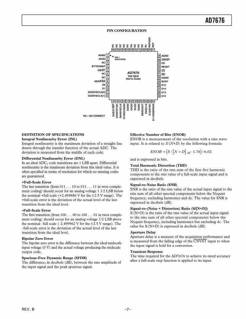
PIN CONFIGURATION
36
35
34
33
32
31
30
29
28
27
26
25
13 14 15 16 17 18 19 20 21 22 23 24
1
2
3
4
5
6
7
8
9
10
11
12
48 47 46 45 44 39 38 3743 42 41 40
PIN 1IDENTIFIER
TOP VIEW(Not to Scale)
AGND
CNVSTPD
RESET
CS
RDDGND
AGND
AVDD
NC
BYTESWAP
OB/2CNC
NC
NC = NO CONNECT
SER/PARD0
D1
D2/DIVSCLK[0]
BUSY
D15
D14
D13
AD7676
D3/DIVSCLK[1] D12
NC
NC
NC
NC
NC
IN+
NC
NC
NC
IN–
RE
FG
ND
RE
F
D4/
EX
T/IN
TD
5/IN
VS
YN
C
D6/
INV
SC
LK
D7/
RD
C/S
DIN
OG
ND
OV
DD
DV
DD
DG
ND
D8/
SD
OU
T
D9/
SC
LK
D10
/SY
NC
D11
/RD
ER
RO
R

REV. B
AD7676
–8–
–Typical Performance Characteristics
CODE
1.00
0 16384 32768 49152 65536
INL
– L
SB
0.75
0.25
0
–0.50
–1.00
0.50
–0.25
–0.75
TPC 1. Integral Nonlinearity vs. Code
CODE IN HEXA
9000
7FFB
0
CO
UN
TS
8000
6000
4000
2000
0000
7000
3000
1000
5000
7FFC
0
7FFD
0
7FFE
8
7FFF
8271
8000
8094
8001
11
8002
0
8003
0
8004
0
TPC 2. Histogram of 16,384 Conversions of a DC Input atthe Code Transition
POSITIVE INL – LSB
20
0.1
NU
MB
ER
OF
UN
ITS
16
8
0
12
4
0.2 0.3 0.4 0.5 0.6 0.7 0.8 0.90 1.0
TPC 3. Typical Positive INL Distribution (199 Units)
CODE IN HEXA
16000
7FFB
0
CO
UN
TS
12000
8000
4000
0000
14000
6000
2000
10000
7FFC
0
7FFD
0
7FFE
880
7FFF 8000
863
8001
0
8002
0
8003
0
8004
0
7FFA
0
14640
TPC 4. Histogram of 16,384 Conversions of a DC Input atthe Code Center
NEGATIVE INL – LSB
20
–0.9
NU
MB
ER
OF
UN
ITS
16
8
0
12
4
–0.8 –0.7 –0.6 –0.5 –0.4 –0.3 –0.2 –0.1–1.0 0.0
TPC 5. Typical Negative INL Distribution (199 Units)
FREQUENCY – kHz
0
0 50 100 150 250
AM
PL
ITU
DE
– d
B o
f F
ull
Sca
le –40
–80
–100
–140
–180
–60
–120
–160
200
–20fS = 500kSPSfIN = 45.01kHzSNR = 94dBTHD = –110dBSFDR = 110dBSINAD = 93.9dB
TPC 6. FFT Plot

REV. B –9–
AD7676
FREQUENCY – kHz
100S
NR
AN
D S
/(N
D
) –
dB
90
70
80
10 10001 100
95
85
75
16.0
EN
OB
– B
its
15.0
13.0
14.0
15.5
14.5
13.5
SNR
S/(ND)
ENOB
TPC 7. SNR, S/(N+D), and ENOB vs. Frequency
INPUT LEVEL – dB
96
SN
R (
RE
FE
RE
NC
ED
TO
FU
LL
SC
AL
E)
– d
B
83
90
–40 0–60 –20
93
87
SNR
–50 –30 –10
S/(ND)
TPC 8. SNR and S/(N+D) vs. Input Level
TEMPERATURE – C
96
SN
R –
dB
84
90
0 125–55 85
93
87
SNR
THD
–35 45 10525–15 65
–104
TH
D –
dB
–112
–108
–106
–110
TPC 9. SNR, THD vs. Temperature
CL – pF
50
t 12
DE
LAY
– n
s
0
20
2000
40
10
10050 150
30
OVDD = 5.0V @ 25C
OVDD = 5.0V @ 85C
OVDD = 2.7V @ 25C
OVDD = 2.7V @ 85C
TPC 10. Typical Delay vs. Load Capacitance CL
SAMPLING RATE – SPS
OP
ER
ATIN
G C
UR
RE
NT
S –
A
0.001
0.1
1M10
100
0.01
1k100 10k
1
100k
10
1k
10k
100k
AVDDDVDD
OVDD
TPC 11. Operating Currents vs. Sample Rate
TEMPERATURE – C
250
PO
WE
R-D
OW
N O
PE
RAT
ING
CU
RR
EN
TS
– n
A
0
100
–15 105–55 45
150
50
DVDD
–35 5 8525 65
200
OVDDAVDD
TPC 12. Power-Down Operating Currents vs. Temperature

REV. B
AD7676
–10–
IN+
REF
REFGND
IN–
32,768C 16,384CMSB
4C 2C C CLSB SW+
SWITCHESCONTROL
32,768C 16,384C
MSB
4C 2C C CLSB SW–
BUSY
OUTPUTCODE
CNVST
CONTROLLOGICCOMP
Figure 3. ADC Simplified Schematic
CIRCUIT INFORMATIONThe AD7676 is a fast, low power, single-supply, precise 16-bitanalog-to-digital converter (ADC). The AD7676 is capable ofconverting 500,000 samples per second (500 kSPS) and allowspower saving between conversions. When operating at 100 SPS,for example, it typically consumes only 15 µW. This featuremakes the AD7676 ideal for battery-powered applications.
The AD7676 provides the user with an on-chip track-and-hold,successive-approximation ADC that does not exhibit any pipelineor latency, making it ideal for multiple multiplexed channelapplications.
The AD7676 can be operated from a single 5 V supply and beinterfaced to either 5 V or 3 V digital logic. It is housed in a48-lead LQFP package or a 48-lead LFCSP package that combinesspace savings and allows flexible configurations as either serialor parallel interface. The AD7676 is pin-to-pin compatible withthe AD7675.
CONVERTER OPERATIONThe AD7676 is a successive-approximation analog-to-digitalconverter based on a charge redistribution DAC. Figure 3 showsthe simplified schematic of the ADC. The capacitive DAC consistsof two identical arrays of 16 binary weighted capacitors.
During the acquisition phase, terminals of the array tied to thecomparator’s input are connected to AGND via SW+ and SW–.All independent switches are connected to the analog inputs.Thus, the capacitor arrays are used as sampling capacitors andacquire both analog signals.
When the acquisition phase is complete and the CNVST inputgoes or is low, a conversion phase is initiated. When the conversionphase begins, SW+ and SW– are opened first. The two capacitorarrays are then disconnected from the inputs and connected tothe REFGND input. Therefore, the differential voltage betweenthe output of IN+ and IN– captured at the end of the acquisitionphase is applied to the comparator inputs, causing the comparatorto become unbalanced.
By switching each element of the capacitor array betweenREFGND or REF, the comparator input varies by binaryweighted voltage steps (VREF/2, VREF/4 . . . VREF/65536). Thecontrol logic toggles these switches, starting with the MSB first,in order to bring the comparator back into a balanced condition.After the completion of this process, the control logic generatesthe ADC output code and brings BUSY output LOW.
Transfer FunctionsUsing the OB/2C digital input, the AD7676 offers two outputcodings: straight binary and twos complement. The ideal transfercharacteristic for the AD7676 is shown in Figure 4.
000...000
000...001
000...010
111...101111...110111...111
ANALOG INPUT
+FS – 1.5 LSB
+FS – 1 LSB–FS + 1 LSB–FS
–FS + 0.5 LSB
AD
C C
OD
E –
Str
aig
ht
Bin
ary
Figure 4. ADC Ideal Transfer Function
TEMPERATURE – C
5
3
–5–55 135–35
LS
B
–15 –5 15 35 55 75 95
1
–1
–3
115
4
2
0
–2
–4
–FS
OFFSET
+FS
TPC 13. Drift vs. Temperature

REV. B
AD7676
–11–
TYPICAL CONNECTION DIAGRAMFigure 5 shows a typical connection diagram for the AD7676.Different circuitry shown on this diagram is optional and isdiscussed below.
Analog InputsThe AD7676 is specified to operate with a differential ±2.5 Vrange. The typical input impedance for each analog input rangeis also shown. Figure 6 shows a simplified analog input sectionof the AD7676.
IN+
IN–
AGND
AVDD
R+ = 684
CS
CS
R– = 684
Figure 6. Simplified Analog Input
The diodes shown in Figure 6 provide ESD protection for theinputs. Care must be taken to ensure that the analog input signalnever exceeds the absolute ratings on these inputs. This willcause these diodes to become forward-biased and start conducting
current. These diodes can handle a forward-biased current of120 mA maximum. This condition could eventually occur whenthe input buffer’s (U1) or (U2) supplies are different fromAVDD. In such a case, an input buffer with a short-circuitcurrent limitation can be used to protect the part.
This analog input structure is a true differential structure. Byusing these differential inputs, signals common to both inputsare rejected as shown in Figure 7, which represents the typicalCMRR over frequency.
FREQUENCY – Hz
CM
RR
– d
B
45
75
10k 10M1k 1M
80
65
100k
55
85
70
60
50
40
Figure 7. Analog Input CMRR vs. Frequency
AVDD AGND DGND DVDD OVDD OGND
SER/PAR
CNVST
BUSY
SDOUT
SCLK
RD
CS
RESET
PD
REFGND
CREF2.5V REF
NOTE 1
REF
100
D
CLOCK
AD7676
C/P/DSP
SERIAL PORT
DIGITAL SUPPLY(3.3V OR 5V)
ANALOGSUPPLY
(5V)
DVDDOB/2C
NOTE 7
BYTESWAP
DVDD
50k
100nF
1M
IN+ANALOG INPUT+
CC 2.7nF
U1NOTE 4
NOTE 5
50
AD8021
–
+
15
NOTE 2
NOTE 3
NOTE 6
ADR421
10F 100nF+10F 100nF
+100nF
+10F
IN–ANALOG INPUT–
CC 2.7nF
U2NOTE 4
NOTE 5
50
AD8021
–
+
15
50
+1F
NOTES1. SEE VOLTAGE REFERENCE INPUT SECTION.2. WITH THE RECOMMENDED VOLTAGE REFERENCES, CREF IS 47F. SEE VOLTAGE REFERENCE INPUT SECTION.3. OPTIONAL CIRCUITRY FOR HARDWARE GAIN CALIBRATION.4. THE AD8021 IS RECOMMENDED. SEE DRIVER AMPLIFIER CHOICE SECTION.5. SEE ANALOG INPUTS SECTION.6. OPTION, SEE POWER SUPPLY SECTION.7. OPTIONAL LOW JITTER CNVST, SEE CONVERSION CONTROL SECTION.
Figure 5. Typical Connection Diagram (±2.5 V Range Shown)

REV. B
AD7676
–12–
During the acquisition phase for ac signals, the AD7676 behaveslike a one-pole RC filter consisting of the equivalent resistanceR+, R–, and CS. The resistors R+ and R– are typically 684 Ω andare lumped components made up of some serial resistors and theon resistance of the switches. The capacitor CS is typically 60 pFand is mainly the ADC sampling capacitor. This one-pole filterwith a typical –3 dB cutoff frequency of 3.88 MHz reduces unde-sirable aliasing effects and limits the noise coming from the inputs.
Because the input impedance of the AD7676 is very high, theAD7676 can be driven directly by a low impedance source withoutgain error. That allows users to put, as shown in Figure 5, anexternal one-pole RC filter between the output of the amplifieroutput and the ADC analog inputs to even further improve thenoise filtering done by the AD7676 analog input circuit. However,the source impedance has to be kept low because it affects theac performances, especially the total harmonic distortion (THD).The maximum source impedance depends on the amount ofTHD that can be tolerated. The THD degrades proportionallyto the source impedance.
Single-to-Differential DriverFor applications using unipolar analog signals, a single-ended-to-differential driver will allow for a differential input into the part.The schematic is shown in Figure 8.
U2
590
5902.5V REF
CC
AD8021
590AD7676
IN+
IN– REF
2.5V REF
U1ANALOG INPUT
(UNIPOLAR)CC
AD8021
590
Figure 8. Single-Ended-to-Differential Driver Circuit
This configuration, when provided an input signal of 0 to VREF,will produce a differential ±2.5 V with a common mode at 1.25 V.If the application can tolerate more noise, the AD8138 can be used.
Driver Amplifier ChoiceAlthough the AD7676 is easy to drive, the driver amplifier needsto meet the following requirements:
• The driver amplifier and the AD7676 analog input circuit haveto be able, together, to settle for a full-scale step of the capaci-tor array at a 16-bit level (0.0015%). In the amplifier’s datasheet, the settling at 0.1% or 0.01% is more commonlyspecified. It could significantly differ from the settling timeat the 16-bit level and, therefore, it should be verified prior tothe driver selection. The tiny op amp AD8021, which com-bines ultralow noise and a high gain bandwidth, meets thissettling time requirement even when used with a high gainup to 13.
• The driver needs to have a THD performance suitable tothat of the AD7676.
• The noise generated by the driver amplifier needs to be keptas low as possible to preserve the SNR and transition noise
performance of the AD7676. The noise coming from the driver isfiltered by the AD7676 analog input circuit one-pole, low-passfilter made by R+, R–, and CS. The SNR degradation due tothe amplifier is:
SNR LOGf N eLOSS
dB N
=+
−
2028
784 32π ( )
where:
f–3 dB is the –3 dB input bandwidth of the AD7676 (3.9 MHz)or the cutoff frequency of the input filter if any is used.
N is the noise factor of the amplifier (1 if in bufferconfiguration).
eN is the equivalent input noise voltage of the op amp in nV/√Hz.
For instance, a driver with an equivalent input noise of2 nV/√Hz like the AD8021 and configured as a buffer, thuswith a noise gain of +1, will degrade the SNR by only 0.26 dB.
The AD8021 meets these requirements and is usually appropriatefor almost all applications. The AD8021 needs an externalcompensation capacitor of 10 pF. This capacitor should havegood linearity as an NPO ceramic or mica type.
The AD8022 could also be used where a dual version is neededand a gain of 1 is used.
The AD8132 or the AD8138 could also be used to generatea differential signal from a single-ended signal.
The AD829 is another alternative where high frequency (above500 kHz) performance is not required. In a gain of 1, it requiresan 82 pF compensation capacitor.
The AD8610 is also another option where low bias current isneeded in low frequency applications.
Voltage Reference InputThe AD7676 uses an external 2.5 V voltage reference.
The voltage reference input REF of the AD7676 has a dynamicinput impedance. Therefore, it should be driven by a low imped-ance source with an efficient decoupling between the REF andREFGND inputs. This decoupling depends on the choice of thevoltage reference but usually consists of a low ESR tantalumcapacitor connected to the REF and REFGND inputs withminimum parasitic inductance. 47 µF is an appropriate value forthe tantalum capacitor when used with one of the recommendedreference voltages:
• The low noise, low temperature drift ADR421 and AD780voltage references
• The low power ADR291 voltage reference
• The low cost AD1582 voltage reference
For applications using multiple AD7676s, it is more effective tobuffer the reference voltage with a low noise, very stable op amplike the AD8031.
Care should also be taken with the reference temperature coeffi-cient of the voltage reference, which directly affects the full-scaleaccuracy if this parameter matters. For instance, a ±15 ppm/°Ctempco of the reference changes the full scale by ±1 LSB/°C.

REV. B
AD7676
–13–
VREF , as mentioned in the specification table, could be increasedto AVDD – 1.85 V. The benefit here is the increased SNR obtainedas a result of this increase. Since the input range is defined interms of VREF, this would essentially increase the range to makeit a ±3 V input range with an AVDD above 4.85 V. The theo-retical improvement as a result of this increase in reference is1.58 dB (20 log [3/2.5]). Due to the theoretical quantization noise,however, the observed improvement is approximately 1 dB. TheAD780 can be selected with a 3 V reference voltage.
Power SupplyThe AD7676 uses three sets of power supply pins: an analog 5 Vsupply AVDD, a digital 5 V core supply DVDD, and a digitalinput/output interface supply OVDD. The OVDD supply allowsdirect interface with any logic working between 2.7 V andDVDD + 0.3 V. To reduce the number of supplies needed, thedigital core (DVDD) can be supplied through a simple RC filterfrom the analog supply as shown in Figure 5. The AD7676 isindependent of power supply sequencing once OVDD does notexceed DVDD by more than 0.3 V and thus free from supplyvoltage-induced latch-up. Additionally, it is very insensitive topower supply variations over a wide frequency range, as shown inFigure 9.
FREQUENCY – Hz
75
PS
RR
– d
B
35
65
10k 10M1k 1M
55
100k
45
70
60
50
40
Figure 9. PSRR vs. Frequency
POWER DISSIPATIONThe AD7676 automatically reduces its power consumption atthe end of each conversion phase. During the acquisition phase,the operating currents are very low, which allows a significantpower savings when the conversion rate is reduced, as shown inFigure 10. This feature makes the AD7676 ideal for very lowpower battery-operated applications.
It should be noted that the digital interface remains active evenduring the acquisition phase. To reduce the operating digitalsupply currents even further, the digital inputs need to be drivenclose to the power rails (i.e., DVDD and DGND) and OVDDshould not exceed DVDD by more than 0.3 V.
SAMPLING RATE – SPS
1M
PO
WE
R D
ISS
IPAT
ION
–
W
0.1
10k
100 100k10 10k
100
1k
1
100k
1k
10
1M
Figure 10. Power Dissipation vs. Sample Rate
CONVERSION CONTROLFigure 11 shows the detailed timing diagrams of the conversionprocess. The AD7676 is controlled by the signal CNVST, whichinitiates conversion. Once initiated, it cannot be restarted oraborted, even by the power-down input PD, until the conversionis complete. The CNVST signal operates independently of CSand RD signals.
CNVST
t1
t2
MODE ACQUIRE CONVERT ACQUIRE CONVERT
t7 t8
BUSYt4
t3
t5
t6
Figure 11. Basic Conversion Timing
For true sampling applications, the recommended operation ofthe CNVST signal is the following:
CNVST must be held HIGH from the previous falling edge ofBUSY, and during a minimum delay corresponding to the acqui-sition time t8; then, when CNVST is brought LOW, a conversionis initiated and the BUSY signal goes HIGH until the comple-tion of the conversion. Although CNVST is a digital signal, itshould be designed with this special care with fast, clean edges,and levels, with minimum overshoot and undershoot or ringing.
For applications where the SNR is critical, the CNVST signalshould have a very low jitter. To achieve this, some use a dedicatedoscillator for CNVST generation or, at least, to clock it with ahigh frequency low jitter clock as shown in Figure 5.

REV. B
AD7676
–14–
t9
RESET
DATABUS
BUSY
CNVST
t8
Figure 12. RESET Timing
For other applications, conversions can be automatically initiated.If CNVST is held LOW when BUSY is LOW, the AD7676controls the acquisition phase and then automatically initiates anew conversion. By keeping CNVST LOW, the AD7676 keepsthe conversion process running by itself. It should be noted thatthe analog input has to be settled when BUSY goes LOW. Also,at power-up, CNVST should be brought LOW once to initiate theconversion process. In this mode, the AD7676 could sometimesrun slightly faster than the guaranteed limit of 500 kSPS.
DIGITAL INTERFACEThe AD7676 has a versatile digital interface; it can be interfacedwith the host system by using either a serial or parallel interface.The serial interface is multiplexed on the parallel databus. TheAD7676 digital interface also accommodates both 3 V or 5 Vlogic by simply connecting the OVDD supply pin of the AD7676to the host system interface digital supply. Finally, by using theOB/2C input pin, either twos complement or straight binarycoding can be used.
The two signals CS and RD control the interface. When at leastone of these signals is HIGH, the interface outputs are in highimpedance. Usually, CS allows the selection of each AD7676 inmulticircuit applications and is held LOW in a single AD7676design. RD is generally used to enable the conversion result onthe databus.
CNVST
BUSY
DATABUS
CS = RD = 0
PREVIOUS CONVERSION DATA NEW DATA
t1
t10
t4
t3t11
Figure 13. Master Parallel Data Timing for Reading(Continuous Read)
PARALLEL INTERFACEThe AD7676 is configured to use the parallel interface (Figure 13)when the SER/PAR is held LOW. The data can be read eitherafter each conversion, which is during the next acquisition phase,or during the following conversion as shown, respectively, inFigures 14 and 15. When the data is read during the conversion,however, it is recommended that it be read-only during the firsthalf of the conversion phase. That avoids any potential feedthroughbetween voltage transients on the digital interface and the mostcritical analog conversion circuitry.
DATABUS
t12 t13
BUSY
CS
RD
CURRENTCONVERSION
Figure 14. Slave Parallel Data Timing for Reading(Read after Conversion)
CS = 0
CNVST,RD
t1
PREVIOUSCONVERSIONDATABUS
t12 t13
BUSY t4
t3
Figure 15. Slave Parallel Data Timing for Reading (Readduring Conversion)
The BYTESWAP pin allows a glueless interface to an 8-bit bus.As shown in Figure 16, the LSB byte is output on D[7:0] and theMSB is output on D[15:8] when BYTESWAP is LOW. WhenBYTESWAP is HIGH, the LSB and MSB bytes are swapped andthe LSB is output on D[15:8] and the MSB is output on D[7:0].By connecting BYTESWAP to an address line, the 16-bit datacan be read in two bytes on either D[15:8] or D[7:0].
CS
RD
BYTE
PINS D[15:8]
PINS D[7:0]HI-Z
HI-ZHIGH BYTE LOW BYTE
LOW BYTE HIGH BYTEHI-Z
HI-Z
t12 t12 t13
Figure 16. 8-Bit Parallel Interface
REV. B
AD7676
–15–
t3
BUSY
CS, RD
CNVST
SYNC
SCLK
SDOUT
1 2 3 14 15 16
D15 D14 D2 D1 D0X
EXT/INT = 0 RDC/SDIN = 0 INVSCLK = INVSYNC = 0
t14
t20
t15
t16t22
t23
t29
t28
t18t19
t21
t30
t25
t24
t26
t27
Figure 17. Master Serial Data Timing for Reading (Read after Conversion)
EXT/INT = 0 RDC/SDIN = 1 INVSCLK = INVSYNC = 0
D15 D14 D2 D1 D0X
1 2 3 14 15 16
BUSY
SYNC
SCLK
SDOUT
CS, RD
CNVST
t3
t1
t17
t14
t15
t19
t20 t21
t16 t22
t23
t24
t27
t26
t25
t18
Figure 18. Master Serial Data Timing for Reading (Read Previous Conversion during Conversion)
SERIAL INTERFACEThe AD7676 is configured to use the serial interface when theSER/PAR is held HIGH. The AD7676 outputs 16 bits of dataMSB first, on the SDOUT pin. This data is synchronized withthe 16 clock pulses provided on the SCLK pin.
MASTER SERIAL INTERFACEInternal ClockThe AD7676 is configured to generate and provide the serial dataclock SCLK when the EXT/INT pin is held LOW. The AD7676 alsogenerates a SYNC signal to indicate to the host when the serial
data is valid. The serial clock SCLK and the SYNC signal can beinverted if desired. The output data is valid on both the risingand falling edges of the data clock. Depending on RDC/SDINinput, the data can be read after each conversion or during thefollowing conversion. Figures 17 and 18 show the detailed timingdiagrams of these two modes.
Usually, because the AD7676 has a longer acquisition phasethan the conversion phase, the data is read immediately afterconversion. That makes the mode master, read after conversion,the most recommended serial mode when it can be used.
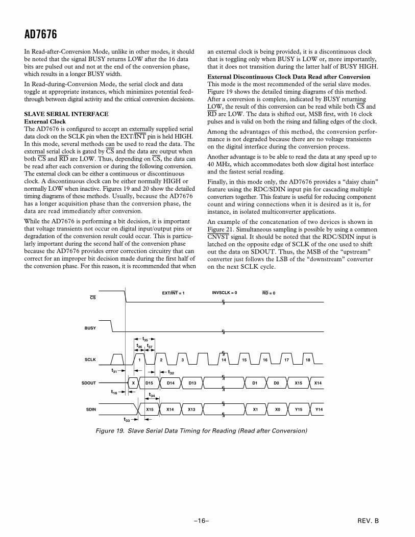
REV. B
AD7676
–16–
In Read-after-Conversion Mode, unlike in other modes, it shouldbe noted that the signal BUSY returns LOW after the 16 databits are pulsed out and not at the end of the conversion phase,which results in a longer BUSY width.
In Read-during-Conversion Mode, the serial clock and datatoggle at appropriate instances, which minimizes potential feed-through between digital activity and the critical conversion decisions.
SLAVE SERIAL INTERFACEExternal ClockThe AD7676 is configured to accept an externally supplied serialdata clock on the SCLK pin when the EXT/INT pin is held HIGH.In this mode, several methods can be used to read the data. Theexternal serial clock is gated by CS and the data are output whenboth CS and RD are LOW. Thus, depending on CS, the data canbe read after each conversion or during the following conversion.The external clock can be either a continuous or discontinuousclock. A discontinuous clock can be either normally HIGH ornormally LOW when inactive. Figures 19 and 20 show the detailedtiming diagrams of these methods. Usually, because the AD7676has a longer acquisition phase than the conversion phase, thedata are read immediately after conversion.
While the AD7676 is performing a bit decision, it is importantthat voltage transients not occur on digital input/output pins ordegradation of the conversion result could occur. This is particu-larly important during the second half of the conversion phasebecause the AD7676 provides error correction circuitry that cancorrect for an improper bit decision made during the first half ofthe conversion phase. For this reason, it is recommended that when
an external clock is being provided, it is a discontinuous clockthat is toggling only when BUSY is LOW or, more importantly,that it does not transition during the latter half of BUSY HIGH.
External Discontinuous Clock Data Read after ConversionThis mode is the most recommended of the serial slave modes.Figure 19 shows the detailed timing diagrams of this method.After a conversion is complete, indicated by BUSY returningLOW, the result of this conversion can be read while both CS andRD are LOW. The data is shifted out, MSB first, with 16 clockpulses and is valid on both the rising and falling edges of the clock.
Among the advantages of this method, the conversion perfor-mance is not degraded because there are no voltage transientson the digital interface during the conversion process.
Another advantage is to be able to read the data at any speed up to40 MHz, which accommodates both slow digital host interfaceand the fastest serial reading.
Finally, in this mode only, the AD7676 provides a “daisy chain”feature using the RDC/SDIN input pin for cascading multipleconverters together. This feature is useful for reducing componentcount and wiring connections when it is desired as it is, forinstance, in isolated multiconverter applications.
An example of the concatenation of two devices is shown inFigure 21. Simultaneous sampling is possible by using a commonCNVST signal. It should be noted that the RDC/SDIN input islatched on the opposite edge of SCLK of the one used to shiftout the data on SDOUT. Thus, the MSB of the “upstream”converter just follows the LSB of the “downstream” converteron the next SCLK cycle.
CS
SCLK
SDOUT D15 D14 D1 D0D13
X15 X14 X13 X1 X0 Y15 Y14
BUSY
SDIN
INVSCLK = 0
X15 X14X
1 2 3 14 15 16 17 18
EXT/INT = 1 RD = 0
t35
t36 t37
t31 t32
t34t16
t33
Figure 19. Slave Serial Data Timing for Reading (Read after Conversion)

REV. B
AD7676
–17–
External Clock Data Read During ConversionFigure 20 shows the detailed timing diagrams of this method.During a conversion, while both CS and RD are LOW, the resultof the previous conversion can be read. The data is shifted out,MSB first, with 16 clock pulses, and is valid on both rising andfalling edges of the clock. The 16 bits have to be read before thecurrent conversion is complete. If that is not done, RDERROR ispulsed HIGH and can be used to interrupt the host interface toprevent incomplete data reading. There is no daisy chain featurein this mode, and RDC/SDIN input should always be tied eitherHIGH or LOW.
To reduce performance degradation due to digital activity, a fastdiscontinuous clock of at least 18 MHz is recommended to ensurethat all the bits are read during the first half of the conversionphase. For this reason, this mode is more difficult to use.
MICROPROCESSOR INTERFACINGThe AD7676 is ideally suited for traditional dc measurementapplications supporting a microprocessor and ac signal processingapplications interfacing to a digital signal processor. The AD7676is designed to interface either with a parallel 8-bit or 16-bit wide
interface or with a general-purpose Serial Port or I/O Ports on amicrocontroller. A variety of external buffers can be used withthe AD7676 to prevent digital noise from coupling into the ADC.The following sections illustrate the use of the AD7676 withan SPI-equipped microcontroller, and the ADSP-21065L andADSP-218x signal processors.
SPI Interface (MC68HC11)Figure 22 shows an interface diagram between the AD7676 and anSPI-equipped microcontroller, such as the MC68HC11. To accom-modate the slower speed of the microcontroller, the AD7676 actsas a slave device and data must be read after conversion. This modealso allows the daisy chain feature. The convert command couldbe initiated in response to an internal timer interrupt. The readingof output data, one byte at a time if necessary, could be initiatedin response to the end-of-conversion signal (BUSY going LOW)using an interrupt line of the microcontroller. The serial periph-eral interface (SPI) on the MC68HC11 is configured for MasterMode (MSTR) = 1, Clock Polarity Bit (CPOL) = 0, Clock PhaseBit (CPHA) = 1, and SPI interrupt enable (SPIE) = 1 by writingto the SPI Control Register (SPCR). The IRQ is configured foredge-sensitive-only operation (IRQE = 1 in OPTION register).
CNVST
SDOUT
SCLK
D1 D0X D15 D14 D13
1 2 3 14 15 16
BUSY
INVSCLK = 0
CS
EXT/INT = 1 RD = 0
t35
t36 t37
t31 t32
t16
t3
Figure 20. Slave Serial Data Timing for Reading (Read Previous Conversion during Conversion)
BUSY BUSY
AD7676 NO. 2(UPSTREAM)
AD7676 NO. 1(DOWNSTREAM)
RDC/SDIN SDOUT
CNVST
CS
SCLK
RDC/SDIN SDOUT
CNVST
CS
SCLK
DATAOUT
SCLK INCS IN
CNVST IN
BUSYOUT
Figure 21. Two AD7676s in a Daisy Chain Configuration

REV. B
AD7676
–18–
AD7676* MC68HC11*
SER/PAR
IRQ
MISO/SDI
SCK
I/O PORT
BUSY
SDOUT
SCLK
CNVST
EXT/INT
CS
RD
INVSCLK
DVDD
*ADDITIONAL PINS OMITTED FOR CLARITY
Figure 22. Interfacing the AD7676 to SPI Interface
ADSP-21065L in Master Serial InterfaceAs shown in Figure 23, the AD7676 can be interfaced to theADSP-21065L using the serial interface in Master Mode withoutany glue logic required. This mode combines the advantages ofreducing the wire connections and the ability to read the data duringor after conversion maximum speed transfer (DIVSCLK[0:1]both LOW).
The AD7676 is configured for the Internal Clock Mode (EXT/INTLOW) and acts, therefore, as the master device. The convertcommand can be generated by either an external low jitter oscil-lator or, as shown, by a FLAG output of the ADSP-21065L or bya frame output TFS of one serial port of the ADSP-21065L thatcan be used like a timer. The Serial Port on the ADSP-21065Lis configured for external clock (IRFS = 0), rising edge active(CKRE = 1), external late framed sync signals (IRFS = 0,LAFS = 1, RFSR = 1), and active HIGH (LRFS = 0). The SerialPort of the ADSP-21065L is configured by writing to its receivecontrol register (SRCTL)—see the ADSP-2106x SHARC User’sManual. Because the Serial Port within the ADSP-21065L willbe seeing a discontinuous clock, an initial word reading has tobe done after the ADSP-21065L has been reset to ensure thatthe Serial Port is properly synchronized to this clock during eachfollowing data read operation.
AD7676* ADSP-21065L*SHARC
SER/PAR
RFS
DR
RCLK
FLAG OR TFS
SYNC
SDOUT
SCLK
CNVST
RDC/SDIN
RD
EXT/INT
CS
DVDD
*ADDITIONAL PINS OMITTED FOR CLARITY
INVSYNC
INVSCLK
Figure 23. Interfacing to the ADSP-21065L Usingthe Serial Master Mode
APPLICATION HINTSLayoutThe AD7676 has very good immunity to noise on the powersupplies as can be seen in Figure 21. However, care should stillbe taken with regard to grounding layout.
The printed circuit board that houses the AD7676 should bedesigned so the analog and digital sections are separated andconfined to certain areas of the board. This facilitates the use of
ground planes that can be easily separated. Digital and analogground planes should be joined in only one place, preferablyunderneath the AD7676, or, at least, as close as possible to theAD7676. If the AD7676 is in a system where multiple devicesrequire analog to digital ground connections, the connectionshould still be made at one point only, a star ground pointthat should be established as close as possible to the AD7676.
It is recommended to avoid running digital lines under the deviceas these will couple noise onto the die. The analog ground planeshould be allowed to run under the AD7676 to avoid noisecoupling. Fast switching signals like CNVST or clocks should beshielded with digital ground to avoid radiating noise to other sec-tions of the board and should never run near analog signal paths.Crossover of digital and analog signals should be avoided. Traceson different but close layers of the board should run at rightangles to each other. This will reduce the effect of feedthroughthrough the board.
The power supply lines to the AD7676 should use as large atrace as possible to provide low impedance paths and reduce theeffect of glitches on the power supply lines. Good decoupling isalso important to lower the supply’s impedance presented tothe AD7676 and reduce the magnitude of the supply spikes.Decoupling ceramic capacitors, typically 100 nF, should beplaced on each power supply’s pins, AVDD, DVDD, and OVDD,close to and ideally right up against these pins and their corre-sponding ground pins. Additionally, low ESR 10 µF capacitorsshould be located in the vicinity of the ADC to further reducelow frequency ripple.
The DVDD supply of the AD7676 can be either a separatesupply or come from the analog supply, AVDD, or from thedigital interface supply, OVDD. When the system digital supplyis noisy, or fast switching digital signals are present, it is recom-mended if no separate supply is available, to connect the DVDDdigital supply to the analog supply AVDD through an RC filter asshown in Figure 5 and to connect the system supply to the inter-face digital supply OVDD and the remaining digital circuitry.When DVDD is powered from the system supply, it is useful toinsert a bead to further reduce high frequency spikes.
The AD7676 has four different ground pins: REFGND, AGND,DGND, and OGND. REFGND senses the reference voltage andshould be a low impedance return to the reference because itcarries pulsed currents. AGND is the ground to which most inter-nal ADC analog signals are referenced. This ground must beconnected with the least resistance to the analog ground plane.DGND must be tied to the analog or digital ground plane,depending on the configuration. OGND is connected to thedigital system ground.
The layout of the decoupling of the reference voltage is important.The decoupling capacitor should be close to the ADC andconnected with short and large traces to minimize parasiticinductances.
Evaluating the AD7676 PerformanceA recommended layout for the AD7676 is outlined in theevaluation board for the AD7676. The evaluation board packageincludes a fully assembled and tested evaluation board,documentation, and software for controlling the board from aPC via the Eval-Control BRD2.

REV. B
AD7676
–19–
OUTLINE DIMENSIONS
48-Lead Plastic Quad Flatpack [LQFP]1.4 mm Thick
(ST-48)Dimensions shown in millimeters
TOP VIEW(PINS DOWN)
1
1213
2524
363748
0.27 0.22 0.17
0.50BSC
7.00BSC
SEATINGPLANE
1.60 MAX
0.750.600.45
VIEW A73.50
0.20 0.09
1.45 1.40 1.35
0.150.05 0.08 MAX
COPLANARITY
VIEW AROTATED 90 CCW
PIN 1INDICATOR
9.00 BSC
COMPLIANT TO JEDEC STANDARDS MS-026BBC
SEATINGPLANE
48-Lead Frame Chip Scale Package [LFCSP](CP-48)
Dimensions shown in millimeters
PIN 1INDICATOR
TOPVIEW
6.75BSC SQ
7.00BSC SQ
148
12
13
3736
2425
BOTTOMVIEW
5.254.702.25
0.500.400.30
0.300.230.18
0.50 BSC
12 MAX
0.25REF
0.70 MAX0.65 NOM1.00
0.900.80
5.50REF
SEATINGPLANE
0.05 MAX0.02 NOM
0.60 MAX0.60 MAX PIN 1
INDICATOR
COMPLIANT TO JEDEC STANDARDS MO-220-VKKD-2
COPLANARITY0.08

REV. B–20–
C02
690–
0–10
/02(
B)
PR
INT
ED
IN U
.S.A
.
Revision HistoryLocation Page
10/02—Data Sheet changed from REV. A to REV. B.
Added 48-Lead LFCSP to FEATURES and GENERAL DESCRIPTION . . . . . . . . . . . . . . . . . . . . . . . . . . . . . . . . . . . . . . . . . . . 1
Added PulSAR Selection table . . . . . . . . . . . . . . . . . . . . . . . . . . . . . . . . . . . . . . . . . . . . . . . . . . . . . . . . . . . . . . . . . . . . . . . . . . . . .1
Edit to SPECIFICATIONS . . . . . . . . . . . . . . . . . . . . . . . . . . . . . . . . . . . . . . . . . . . . . . . . . . . . . . . . . . . . . . . . . . . . . . . . . . . . . . .2
Changes to ABSOLUTE MAXIMUM RATINGS . . . . . . . . . . . . . . . . . . . . . . . . . . . . . . . . . . . . . . . . . . . . . . . . . . . . . . . . . . . . . .4
Additions to ORDERING GUIDE . . . . . . . . . . . . . . . . . . . . . . . . . . . . . . . . . . . . . . . . . . . . . . . . . . . . . . . . . . . . . . . . . . . . . . . . . .4
Edits to PIN FUNCTION DESCRIPTIONS . . . . . . . . . . . . . . . . . . . . . . . . . . . . . . . . . . . . . . . . . . . . . . . . . . . . . . . . . . . . . . . . . .5
Edit to Transfer Functions section . . . . . . . . . . . . . . . . . . . . . . . . . . . . . . . . . . . . . . . . . . . . . . . . . . . . . . . . . . . . . . . . . . . . . . . . .10
Changes to Power Supply section . . . . . . . . . . . . . . . . . . . . . . . . . . . . . . . . . . . . . . . . . . . . . . . . . . . . . . . . . . . . . . . . . . . . . . . . . .13
Added 48-Lead Frame Chip Scale Package (LFCSP) . . . . . . . . . . . . . . . . . . . . . . . . . . . . . . . . . . . . . . . . . . . . . . . . . . . . . . . . . . . 19

Mouser Electronics
Authorized Distributor
Click to View Pricing, Inventory, Delivery & Lifecycle Information: Analog Devices Inc.:
AD7676ASTZ