a 3u cubesat platform for plant growth experiments
TRANSCRIPT

Rochester Institute of Technology Rochester Institute of Technology
RIT Scholar Works RIT Scholar Works
Theses
12-13-2019
A 3U Cubesat Platform for Plant Growth Experiments A 3U Cubesat Platform for Plant Growth Experiments
Jared A. Loewenthal [email protected]
Follow this and additional works at: https://scholarworks.rit.edu/theses
Recommended Citation Recommended Citation Loewenthal, Jared A., "A 3U Cubesat Platform for Plant Growth Experiments" (2019). Thesis. Rochester Institute of Technology. Accessed from
This Thesis is brought to you for free and open access by RIT Scholar Works. It has been accepted for inclusion in Theses by an authorized administrator of RIT Scholar Works. For more information, please contact [email protected].

RIT
A 3U Cubesat Platform for Plant Growth Experiments
by
Jared A. Loewenthal
A Thesis Submitted in Partial Fulfillment of the Requirements for
the
Degree of Master of Science in Electrical Engineering
Department of Electrical and Microelectronic Engineering in
Kate Gleason College of Engineering
Rochester Institute of Technology
Rochester, NY
December 13, 2019

ii
A 3U Cubesat Platform for Plant Growth Experiments Jared A. Loewenthal
Committee Approval:
We the undersigned committee members, certify that Jared A. Loewenthal has completed the
requirements for the Master of Science degree in Electrical Engineering.
Dr. Dorin Patru, Graduate Research Advisor Date
Associate Professor, Department of Electrical and Microelectronic Engineering
Professor Mark Indovina Date
Senior Lecturer, Department of Electrical and Microelectronic Engineering
Professor Carlos Barrios Date
Visiting Lecturer, Department of Electrical and Microelectronic Engineering
Dr. Michael Zemcov Date
Assistant Professor, School of Physics and Astronomy
Dr. Jeffrey Mills Date
Senior Lecturer, School of Chemistry and Materials Science
Dr. Sohail Dianat, Department Head Date
Professor, Department of Electrical and Microelectronic Engineering

iii
Table of Contents 1. Abstract ..................................................................................................................... 1
2. Introduction ............................................................................................................... 2
2.1. The Importance of the Cubesat ................................................................................. 2
2.2. The Scientific Goal ................................................................................................... 2
2.3. The Engineering Goal ............................................................................................... 3
2.4. How the Collected Information will be Used ........................................................... 3
3. Background ............................................................................................................... 4
3.1. Past Student Cubesat Designs ................................................................................... 4
3.2. Design Process .......................................................................................................... 4
3.3. Major 3U Cubesat Requirements .............................................................................. 5
3.4. Scientific Payload Requirements .............................................................................. 6
3.5. Additional Engineering Requirements ...................................................................... 7
4. Cubesat Overview ..................................................................................................... 8
4.1. Full 3D Model from Several Angles ......................................................................... 9
5. Mechanical Structure Supporting the Scientific Payload ....................................... 11
5.1. Mechanical Structure Block Diagram ..................................................................... 12
5.2. Mechanical Structure Overview ............................................................................. 13
5.3. Stock Material Needed ............................................................................................ 13
5.4. Manufacturing Process............................................................................................ 13
5.5. Rail .......................................................................................................................... 14
5.6. End Chamber Plate ................................................................................................. 14
5.7. Top and Bottom Chamber Tube Sections with O-Rings ........................................ 15
5.8. Corner Mount .......................................................................................................... 15
5.9. Thermal Management and Profile .......................................................................... 16

iv
6. Top Electronics Board ............................................................................................ 17
6.1. Top Electronics Sensors .......................................................................................... 18
6.2. I2C Sensor Schematics ............................................................................................ 19
6.3. CO2 Sensor .............................................................................................................. 20
6.4. Grow Lights ............................................................................................................ 20
6.5. Camera .................................................................................................................... 21
6.6. Camera Lights ......................................................................................................... 22
6.7. Top Electrical PCB Layout for One Chamber ........................................................ 23
6.8. Mounting the Top Electronics Board ...................................................................... 24
7. Bottom Electronics Board ....................................................................................... 25
7.1. Soil Temperature Sensor ......................................................................................... 26
7.2. Soil Moisture Sensing ............................................................................................. 27
7.3. pH Sensing .............................................................................................................. 28
7.4. Bottom Electrical PCB Layout for One Chamber .................................................. 30
7.5. Mounting the Bottom Electronics Board ................................................................ 30
8. Computer Interface Board....................................................................................... 32
8.1. Board Overview ...................................................................................................... 32
8.2. I2C and UART Communications ............................................................................ 33
8.3. Camera to Pi Interface ............................................................................................ 34
8.4. Connections............................................................................................................. 35
8.5. Computer Radiation Resistance .............................................................................. 36
9. Raspberry Pi Software ............................................................................................ 37
9.1. Pi Startup and Logging Steps .................................................................................. 37
9.2. Pi Computer Execution Flow Chart ........................................................................ 38
9.3. Pi Communication Screenshots .............................................................................. 39

v
10. Side Electronics Power Board ................................................................................ 43
10.1. Buck Boost DC-DC Converters .............................................................................. 44
10.2. Solar Panels ............................................................................................................. 45
10.3. Maximum Power Point Controller .......................................................................... 46
10.4. Lithium Ion Batteries .............................................................................................. 47
10.5. Power Distribution .................................................................................................. 48
10.6. I2C Connections ...................................................................................................... 48
11. pH Sensor Research ................................................................................................ 49
11.1. General pH Information and Existing Sensors ....................................................... 49
11.2. pH Measurement Goal ............................................................................................ 51
12. Tests, Results, and Discussions .............................................................................. 52
12.1. Equipment Used ...................................................................................................... 52
12.2. Mechanical Sealing Check ...................................................................................... 52
12.3. Top Electronics Board Test .................................................................................... 54
12.4. Interface Board........................................................................................................ 54
12.5. Ground Based Plant Testing with Top Chamber Board ......................................... 54
12.6. Side Electronics Board Testing ............................................................................... 57
12.7. Power Used and Budget .......................................................................................... 59
13. Future Work ............................................................................................................ 60
13.1. Radio Communications ........................................................................................... 60
13.2. Attitude Determination and Control System........................................................... 61
13.3. Sensor Additions ..................................................................................................... 62
13.4. Future Tests ............................................................................................................. 62
14. Conclusions ............................................................................................................. 64
15. References ............................................................................................................... 65

vi
Acknowledgements I would like to thank the following people for supporting me throughout my thesis work:
My thesis advisor, Dr. Dorin Patru for providing me guidance and support as I explored
various engineering designs and discovered many problems along the way.
Dr. Sandra Connelly for initially indicating a need for more plant-based space experiments
and providing Cubesat payload goals and requirements.
Dr. Jeffrey Mills for diving right into research and prototyping a pH sensor that could be
useful in the small plant growth chamber.
Students, Spencer Bradshaw and Laura Branch for supporting the testing of a few plant-
growth experiments within the initial Cubesat design.
The RIT KGCOE machine shop for creating the mechanical assembly parts from stock
metal and providing advice on how to seal the chambers from pressure differences. Advice
provided by: Jan Maneti, Craig Arnold, and Ricky Wurzertz
The RIT CEMA surface mount technology lab and the supporting lab manager, Jeffrey
Lonneville.
Electrical Engineering faculty, Ken Snyder for ordering parts to the design such as printed
circuit boards, electronic components, and the stock metal.
Dr. Michael Zemcov and Mark Indovina for serving on the thesis review committee.
My parents and sister for supporting me not only throughout my thesis but the entirety of
my academics at RIT.

1
1. Abstract
This thesis work presents the design, manufacturing, and ground testing of a 3U Cubesat
platform intended for plant growth experiments. The structure is comprised of four identical,
but independent plant growth chambers. Each of these accommodates about two cubic inches
of soil, and the necessary air volume and moisture regulation to grow a fast-growing plant from
seed to seed in 3-4 weeks. The plant growth is artificially stimulated by an array of light
emitting diodes (LEDs) at grow light wavelengths that match the properties of chlorophyll,
and is monitored by a suite of sensors: temperature, pressure, relative humidity, CO2, custom
designed soil pH, soil moisture, and imaging. The latter takes periodic still pictures in the
visible and infrared spectrum using LED based illumination at different wavelengths. These
images are used to analyze the overall health of the plant and record the developmental stages
of the plant growth. The platform is complemented with a raspberry Pi on board computer and
a solar panel-based power generation system. The current scientific goal of this 3U Cubesat
platform is to study the interactions of soil microbes (bacteria and fungus) and plants. The
former can be a source of nutrients for plants and decrease induced stress on these in space
conditions. The availability of four test chambers allow scientists to quantify changes and
investigate emergent properties of the soil bacterial and fungal populations. The Cubesat
design affords the opportunity to investigate the impact of physical factors such as pressure,
temperature, microgravity, and space radiation on the soil bacteria and fungi, in addition to the
overall plant health. While small scale biology experiments have been performed on Cubesats
before, to our knowledge none of those involved plant growth stimulation and monitoring. This
platform can be adapted and expanded to meet the requirements of similar scientific research.

2
2. Introduction
2.1. The Importance of the Cubesat
The Cubesat is one type of mini-satellite that plays an important role in testing a wide
variety of scientific experiments that orbit around the Earth. Originally designed to test
communication electronics in space at an academic level, it has fully expanded to be a solution
for several academic and commercial groups to take advantage of when they want to conduct
experiments in space. Today, Cubesats provide a common method for a small satellite to be
launched into space with relatively little cost and possibly at higher quantities. Researching
physical, biological, and electrical unknowns in space can expand knowledge in unexplored
fields and applications.
2.2. The Scientific Goal
The scientific goal of the Cubesat payload is to study the interactions of soil microbes and
plants to understand what the optimal concentration of beneficial microbes is when in space
conditions, that maximizes nutrient uptake in plant roots and increases overall plant fitness.
Changes in the environment and microbiome community health stem from the interplay
between soil and plant properties such as growth, death, mutation rates, and metabolism of
each microbe species. The Cubesat design gives the opportunity to investigate the impact of
sealed plant growth chambers trying to perform their duty in a space environment
(microgravity and radiation effects). The core question from a scientific point of view is: what
is the optimal concentration of beneficial microbes in space conditions, to maximize nutrient
uptake in plant roots, concomitantly increasing plant fitness (survival and reproduction)?
Plant health can be monitored by various sensor readings; temperature, relative humidity,
carbon dioxide, soil temperature, moisture and pH. The monitored values can correlate to rates
of photosynthesis, pathogen multiplication, and transpiration, which are all indicators of how
a plant and it’s supporting microbiome are doing. For instance, the pH values might vary
between the levels of 8 to 12 based upon the plants preferred bacteria within a specific soil
constitution and change as the plant grows while consuming nutrients provided by the
microbiome. Different plant types prefer growing in different climates and the temperature
plus relative humidity readings can monitor that the environment stays unchanged. The carbon

3
dioxide readings should indicate that the plant is slowly absorbing the molecule resource from
the air as it grows and at what rate. It could be necessary to add an oxygen sensor to monitor
the O2 levels as the plants grow and emit the molecule as a by-product.
Plants can be photographed in order to correlate Camera images looking at the intensity of
various light wavelengths reflecting off of the leaves as the plant grows can provide
information about the plant health across its different regions like the stem, leaves, and flowers.
This characterization can be done for white light (visible light; 400 nm to 750 nm) and near
infrared light (~750 nm to 2.5 um) each representing a different correlation to plant health.
2.3. The Engineering Goal
The major engineering goal of the project is to design, construct, and test a 3U Cubesat
structure that can accommodate a plant growth experiment and can be modified to be tested on
a high-altitude balloon platform. The Cubesat structure will be custom made to integrate a
plant chamber-based payload while incorporating other Cubesat related electronics. The design
should be student / university friendly with thorough documentation alongside a
straightforward material acquisition, manufacturing, and assembly process. The overall costs
of all materials should be low when compared to commercial Cubesat components.
Keeping the design simple will allow for slight modifications and improvements that may
be necessary when adjusting to a specific payload or different data collection. The Cubesat
must be created based on the following requirements and for all general purposes, must fit
within the Cubesat orbital deployer (P-POD) even though other launch solutions exist.
2.4. How the Collected Information will be Used
Anyone who thinks about space exploration realizes that one critical aspect of going further
than ever before requires having a renewable food source. By conducting more plant
experiments in space, it is possible to make breakthroughs in understanding what is the most
practical way to grow healthy, fulfilling food in space. Organism responses to low gravity and
high radiation are poorly studied and highly variable. In general, understanding how space
conditions may stress plants, and learning methods to overcome them will influence space
exploration travel, colony setup, and maintenance, since plants can be protected. Any attempt
to start a farming operation in space will require understanding how plants and soil
communities interact in this low gravity environment and how it influences their growth.

4
3. Background
3.1. Past Student Cubesat Designs
Rochester Institute of Technology has had several student-led projects before in relation to
Cubesats. These projects tested a variety of different elements of a Cubesat and their
applications. RIT Multidisciplinary Engineering (EDGE) project P13271 involved designing
appropriate maximum power point tracking with solar panels on different Cubesat surfaces [1].
EDGE projects P16102 and P16103 worked on a baseline mechanical construction to 1U
Cubesats [2] and a vibration testing rig [3]. EDGE projects P18101 and P19101 worked on
Solar Sails of Cubesats [4] [5]. There were also a few past RIT EDGE projects involving high-
altitude balloon experiments which can be considered a good first step in student-led projects
that work towards designing practical Cubesats. One such project was P19104 which involved
designing a high-altitude balloon instrumentation platform for bio-experiments [6]. This
specific project has similar biology goals and intentions as the one defined in this thesis.
There are other United States university student projects involving the design and creation
of Cubesats. These universities usually have some form of aerospace program that leads to
classes and clubs where Cubesat design is flourishing. Some of these programs and projects
include open source Cubesat designs and software from Capitol Technology and small
satellites made with student run groups at University of Buffalo.
3.2. Design Process
The design mentioned in this paper does not cover all of the design process steps taken to
reach the implementation. Key past design elements are mentioned but not all of the problems,
troubleshooting, and iterations are covered in order to maintain some brevity. Some
requirements changed overtime to better fit the scope of the project and things discovered. The
main design software used in the design process to create the mechanical and electrical
elements was Autodesk Fusion 360 (initially Autodesk Inventor) and Autodesk Eagle PCB
with student, non-commercial licenses.
The manufacturing of the mechanical components was overseen by the student and while
the manufacturing of the printed circuit boards (PCBs) was done through a 3rd party company,
assembly of the components onto the PCBs were completed by the student.

5
3.3. Major 3U Cubesat Requirements
The 3U Cubesat needs to meet the official CubeSat Design Specifications [7] along with
the payload requirements and additional engineering technical constraints. These requirements
are categorized and listed below:
1. Total Chemical Energy Must Not Exceed 100 Watt-Hours
2. CubeSat Materials must satisfy low-outgassing
3. General guidelines for materials used in a vacuum [8]
4. All parts shall remain attached to the CubeSats during launch, ejection and operation
5. No pyrotechnics shall be permitted
6. Propulsion systems shall have at least 3 inhibits to activation
7. Rails shall have a minimum width of 8.5mm
8. Rails will have a surface roughness less than 1.6 µm
9. The edges of the rails will be rounded to a radius of at least 1 mm
10. The maximum mass of a 3U CubeSat shall be 4.00 kg
11. Mass can be exceeded with approval for certain missions
12. Deployables (such as antennas) shall be constrained by the CubeSat, not the P-POD
13. Aluminum 7075, 6061, 5005, and/or 5052 will be used for both the main CubeSat structure
and the rails
14. The CubeSat rails and standoff, which contact the P-POD rails and adjacent CubeSat
standoffs, shall be hard anodized aluminum to prevent any cold welding within the P-POD
15. Separation springs are not required for 3U CubeSats
16. The CubeSat shall have, at a minimum, one deployment switch on a rail standoff
17. If the CubeSat deployment switch toggles from the actuated state and back, the
transmission and deployable timers shall reset to t=0
18. The CubeSat shall include a remove before flight (RBF) pin
19. The CubeSat will have one RF inhibit and RF power output of no greater than 1.5W at the
transmitting antenna’s RF input
20. CubeSats shall incorporate battery circuit protection for charging/discharging to avoid
unbalanced cell conditions
21. All deployables such as booms, antennas, and solar panels shall wait to deploy a minimum
of 30 minutes after the CubeSat's deployment switch(es) are activated from PPOD ejection

6
22. No CubeSats shall generate or transmit any signal from the time of integration into the
PPOD through 45 minutes after on-orbit deployment from the P-POD. However, the
CubeSat can be powered on following deployment form the P-POD
23. General dimensions from the 3U Cubesat assembly specification should be followed
3.4. Scientific Payload Requirements
The scientific experimental platform consists of four plant growth chambers.
Each chamber will:
24. be sealed, maintaining around one atmosphere internal pressure compared to the external
vacuum of space
25. be divided into two sections to make it easy to plant and constrain the soil into one volume
in the chamber
26. be individually monitored with sensors
27. have multiple air temperature sensors
28. have a relative humidity sensor, a pressure sensor, and a carbon dioxide (CO2) sensor to
monitor the chamber air
29. have controllable RGB LEDs to emit a plant growth light at a usual cycle of 18 hours on
and 6 hours off
30. have a camera that is sensitive to both visible and infrared lights
31. have at least one white light source, and one infrared light source to be used by the camera
when taking pictures
32. be internally reflective to increase transfer of light from emitting source to plant
33. have sensors capable of monitoring soil temperature, soil moisture, and soil pH levels
34. be contained so that the plant creates its own habitat / environment to grow in
35. be resistant to drastic internal temperature changes and stay within 15 – 30 degrees Celsius
(could change in future depending on the plant type used)
36. have all the initial water, soil, air composition that the plant will require throughout its
entire life cycle (from seed to flower)

7
3.5. Additional Engineering Requirements
37. Power should be generated from solar panels and stored in lithium ion batteries
38. No unnecessary wiring between boards or items should be used in design
39. The 3U Cubesat should communicate on the 2 meter and 70 cm amateur radio bands
40. The Cubesat must support having an attitude determination, and control system (ADCS)
The thesis goes on to describe the design, implementation, and testing of the 3U Cubesat
in the following sections.

8
4. Cubesat Overview
The block diagram below shows the stack up of key components in the designed Cubesat:
Figure 1: Cubesat System contained with Mechanical Structure
The two reserved sections, the ADCS and radio communications, were not fully designed
but various options were considered as described in the
Future Work section.

9
4.1. Full 3D Model from Several Angles
Figure 2: Cubesat Side Angle 1
Pi 3B+ Computer
Solar Pannels
Chambers
Rails

10
Figure 3: Cubesat Side Angle 2
Top Electronics
Bottom Electronics

11
5. Mechanical Structure Supporting the Scientific Payload
The scientific payload consists of four plant growth chambers that are each about 8.5” tall,
with a diameter of 1.25” which is enough volume for petite fast plants to grow within. Each
sealed chamber is designed to meet the requirements listed above. Each has a bottom soil
section (the lower part of the chamber) while the rest of the free space gives room for the plant
to grow. The four-chamber structure has been designed to attach to the Cubesat rails for full
integration. The CAD screenshot below shows the main payload structure attached to the
Cubesat rails.
Figure 4: Cubesat Mechanical Structure
Top Chambers
Bottom Chambers
Rails

12
5.1. Mechanical Structure Block Diagram
The block diagram below shows the structure general layout with a side view. The end
chamber mount plates compress the chamber tube sections when screwed to the corner mounts,
which are fixed to the rail with other hardware. Arrows represent main screw forces.
Figure 5: Mechanical Side View Diagram (not to scale)

13
5.2. Mechanical Structure Overview
The mechanical structure of the Cubesat is defined by the Cubesat standard, with the focus
being on using aluminum 6061, meeting the dimensional tolerances of a 3U Cubesat, and
creating four sealable chambers. The main focus of the design is the payload so creating an
easy way to fill, assemble, and seal the four chambers was critical in the design integration.
Accessible stock materials were used and only basic machinery (mills and lathes) were needed
to create the structure.
5.3. Stock Material Needed
The following list describes the materials used when creating the structure
41. 6061 Aluminum ¾” 90-degree Rails
42. ¼” Thick 6061 Aluminum Plate
43. 1.5” OD, 1.25” ID 6061 Aluminum Hollow Tube
44. 1.125” O-rings
45. ¼” -20 Screws
46. 6 -32 Screws
5.4. Manufacturing Process
Each part item in CAD was turned into a drawing which a machine shop was able to use
in order to cut, drill, and turn a part to the required dimensions. The main parts include the
rails, the bottom and top chamber plates, the top chamber sections, the bottom chamber
sections, the chamber mating plate, and the chamber to rail mounts. All parts could be made
from the acquired materials following subtractive manufacturing using basic machines and
standard cutting implements. The O-rings were used to seal between the cylinder chambers
and each aluminum plate. All four chambers were kept aligned with each other through the use
of each plate connecting to all four chambers. The rails could be annealed separately after
manufacturing or annealed versions of the stock rail could be pre-bought. The rails need to be
annealed to meet the Cubesat standard. The following CAD screenshots show key parts before
assembly.

14
5.5. Rail
Figure 6: Cubesat Rail
5.6. End Chamber Plate
Figure 7: Cubesat End Chamber Plate
12.9” Long
Each Chamber Tube
Section is Inserted Here
3.8” Per Side

15
5.7. Top and Bottom Chamber Tube Sections with O-Rings
Figure 8: Chamber Tube Sections
It is worth noting that the Top Chamber Section (on right) has inner material removed
initially for significant mass savings, but also to allow other electronic components to fit into
certain spaces.
5.8. Corner Mount
Figure 9: Cubesat Corner Mount
6.25” Long
1.5” Long
1.25” Inner Diameter
O-Ring
0.75” Per Side

16
5.9. Thermal Management and Profile
The aluminum Cubesat body has not yet been thermally profiled and characterized in order
to determine the most effective thermal management for the Cubesat at a high altitude or in
orbit. The solar panels, batteries, future communication system, and powered electronics will
also impact thermal management. Classifying the mechanical structure is the first step. These
thermal profiles are typically conducted on the entire system before it’s flown in space.
It is important that the internal components of the sealed chambers (the soil, air, and plant
itself) stay within the temperature range that the plants can tolerate, usually in the range of 15
to 30 degrees Celsius. The atmosphere within each chamber acts as a thermal mass that can
resist fast changes for a typical 90-minute orbit cycle but since the outside of each chamber is
aluminum, it needs to be profiled carefully. So far nothing has been done to test space-like
temperature conditions on the Cubesat in software or in a real-life test and if there is an issue,
design changes need to be made to alleviate drastic temperature changes of the chamber. Due
to the relatively low power draw of the Cubesat chamber electronics, as mentioned in the Power
Used and Budget section, the mechanical structure, computer-generated heat, and surface solar
panels are currently the biggest concerns during a characterization of the Cubesat.
A computational fluid dynamics (CFD) profile should be created for the structure to
determine if an active thermal management is necessary. The model needs to consider all active
and passive heat sources, all heat conduction paths through the structure, and all available heat
dissipation through radiation surfaces. Peltier elements could be used to for active heat transfer.

17
6. Top Electronics Board
The top electronics printed circuit board (PCB) mounts on top of the top chamber plate in
order to provide sensors into the chambers and a camera imaging solution. The board also
mounts RGB LED grow lights, so the plants can absorb energy through photosynthesis and
grow. The board seals the top of the structure by using a laser cut rubber gasket, made out of
the same material as the O-rings. The block diagram below shows the key components and
connections of the board.
Figure 10: Top Electronics Board Block Diagram

18
Figure 11: Top Chamber Board View of Inside Chamber Electronics
6.1. Top Electronics Sensors
The sensors used to monitor the air are as follows:
1. An ADT7420 Temperature Sensor [9]
2. A MS5607-02BA Pressure Sensor [10]
3. A SHT31 Relative Humidity Sensor [11]
4. A CO2IR-LP Carbon Dioxide Sensor [12]
Each chamber has its own set of sensors. The dedicated temperature sensor measures
temperature very accurately, but the other three sensors can also measure and return
temperature information. The pressure sensor monitors the chamber absolute pressure level to
ensure that there is no vacuum leak once the chamber is sealed, while all the other sensors
monitor the air quality over time, to provide information on the environment that the plant is
growing in. The CO2 sensor communicates via a serial UART connection, while all other
sensors connect to a computer via I2C protocol.
CO2 Sensor
Camera
RGB Grow LEDs
Rubber Gasket

19
There are many sensors that have the same features as those that were chosen. Some of the
sensor integrated circuits (ICs) that are picked were used during tests in previous graduate
work, while others like the CO2 sensor were picked after finding an off the shelf part that has
a small form factor, easy communications, and consumed relatively little power.
6.2. I2C Sensor Schematics
The I2C sensor schematics below show typical connections via the I2C protocol. There are
one microfarad decoupling capacitors on each of the power inputs as specified by the
datasheets. The relative humidity sensor has a shunt resistor to limit the reset current. All three
I2C sensors have an operating temperature range of at least -40 to +85 degrees Celsius (C). The
temperature sensor can measure between -20 to +105 C, while the relative humidity sensor can
measure from 0-100% RH within that the temperature range. The pressure sensor can
determine pressure values between 10 and 1200 mbar which covers the 1 atmosphere chamber
pressure designed for. The I2C channel can communicate at 1 MHz between all of the sensors.
Figure 12: I2C Sensor Schematics

20
6.3. CO2 Sensor
The CO2 sensor operates from at least 0 to +50 C (which is good enough for the expected
range of the sealed chambers) and measures the carbon dioxide levels from about 0 to 5000
parts per million (ppm). Monitoring CO2 levels at low power with infrared technology can
show that the growing plants are slowly using the CO2 up in the sealed chamber. The schematic
is shown below.
Figure 13: CO2 Sensor Schematic
6.4. Grow Lights
After some initial testing, through hole RGB LED lights were chosen to be the main source
of energy for the plants to grow, grow lights. The WP154A4SUREQBFZGC were picked since
their wavelength produced the red and blue colors that mostly match the standard chlorophyll
absorption spectrum [13]. LP55231s were chosen to drive the LEDs at various power / current
levels using I2C communication by the on-board computer. Multiple of these drivers (up to
four) can be put in parallel to support more than 3 RGB LEDs, since each one’s address is
different. Therefore, six RGB LEDs and two associated drivers are used in each grow chamber.
A schematic for one driver set is shown below.
Figure 14: RGB LED Driver Configuration

21
6.5. Camera
In order to find a student accessible, mostly non-proprietary camera, that was small enough
to fit on the top electronic board form factor. The camera had to be sensitive to both visible
and infrared light, so a raspberry Pi camera version 2 was deemed most appropriate. Off-the-
shelf no infrared filter (NoIR) Pi camera boards are sensitive to both wavelength bands, visible
and infrared, and can be bought from several different sources [14]. The camera module itself
is removed from the commercial board and placed onto the custom top electronics board since
the circuitry was designed to functionally match the posted schematic [15]. The top electronics
camera schematic section is shown below. It has dual-inductor common-mode chokes for the
differential pair signals and a 24 MHz oscillating clock.
Figure 15: Camera Connections Schematic
Using the Pi camera has the drawback of forcing the design to use a recent raspberry Pi
computer board with the official Raspbian operating system (OS) software in order to take
pictures and video. The ATSHA204A IC chip has to be moved from the commercial board
onto the equivalent circuitry in order to allow the raspberry Pi computer to properly id the
camera and not lock up when attempting to connect to it. The custom memory chip is pre-
programmed with the required information to communicate with the raspberry Pi and cannot
be bought separately, since it would arrive blank. It could be possible to replicate the
information with a programmable computer, if it becomes a requirement in the future, but it is
not necessary for this design.

22
6.6. Camera Lights
In order to capture images of the plants in the chambers with the camera, light emitting
sources needed to be added to the top electronics board. Both white LEDs and infrared surface
mount LEDs are added. The chosen L130 white LEDs come in different temperatures [16].
One 5000K and one 6500K are used on the electronics board, driven by another LP55231 LED
driver. The two plain surface mount infrared LEDs are also driven by the constant current
driver, as shown in the schematic.
Figure 16: Camera LED Driver Schematic
The infrared light is captured in a still picture and can help determine general plant health
based on reflections of the light off the stem, leaves, and flowers.

23
6.7. Top Electrical PCB Layout for One Chamber
The layout for the circuitry of each chamber is almost identical, except for the connections
to the connecting headers, such as JP1 on the left. A screenshot of the PCB is provided below.
It should be noted that the three camera signal pairs were routed as differential pairs because
of the camera standard used in the Pi to camera communication protocol. Red colors indicate
components located outside of the chambers, while blue indicates components on the inside.
The large dashed yellow outline represents the border of the 3.3V plane while the dashed
orange border (which goes around the whole board) represents the common ground plane. The
power rails to the camera also use the power layer with shorter sections. These can be seen
extending out from the bottom left where the camera power connector is.
Figure 17: Top Electronics Board PCB Layout

24
6.8. Mounting the Top Electronics Board
The PCB is snuggly screwed down to the end chamber top plate where a laser cut gasket
is put in between. Epoxy is used to cover over the vias and through holes to create and complete
the chamber seal.
Figure 18: Mounted Top Electronics Board

25
7. Bottom Electronics Board
The bottom electronics PCB mounts on the bottom chamber plate and contains three
sensors that are embedded in the soil. Temperature, soil moisture, and pH sensors provide
useful information when growing the plants in each chamber. Each sensor type communicates
with the computer via I2C communications. This board is also fully sealed by applying a cover
coat of epoxy on the outside after it is mounted. The block diagram below shows the key
components and connections of the board.
Figure 19: Bottom Electronics Block Diagram

26
Figure 20: 3D Model of Bottom Electronics Board
7.1. Soil Temperature Sensor
A TC74 chip is used to monitor temperature in the soil [17]. It should fluctuate slowly due
to the wide metal contact area of the TO-220 package type that will be embedded in the soil.
It also works better with its I2C communication interface, than a 1-wire interface.
Figure 21: Soil Temperature IC
Soil Tempearature Sensor
pH Probes
Soil Moisture Probes

27
7.2. Soil Moisture Sensing
The soil moisture sensor circuitry is based on a capacitive measuring approach instead of
a resistive one. It consumes less power to take a measurement and the probes have even less
of a chance of becoming corroded over time, since they are already stainless steel. The moist
soil acts as a variable dielectric material and the measurement process cannot affect the soil
microorganisms as much as the resistive approach. The following schematic shows the use of
a 555-timer chip to generate a frequency pulse to the probes (represented by the S1 capacitor
symbol), which can be monitored by the I2C analog-to-digital converter (ADC). This is based
on the Capacitive Soil Moisture Sensor from DF Robot company [18]. The first circuit design
originally measured rise and fall times of the anticipated microfarad capacitances, however it
became impractical to properly obtain multiple ADC values at specific intervals. Switches
were used to charge and discharge the stainless-steel probes acting as the capacitor plates.
Figure 22: Soil Moisture Schematic

28
7.3. pH Sensing
The development of a miniature pH sensor that could be embedded in the soil of each
chamber required a lot of research. This is expanded on in pH Sensor Research, while the
circuitry that measures the pH on the bottom electrical board is discussed here. A pH sensor is
comprised of the working / active electrode and the reference electrode. Measuring the voltage
across these two electrodes when they are both in the same solution corresponds to a pH value.
The values are determined by pre-calibration in known pH solution buffers. To simplify the
readings and to account for the potentially negative values, the reference voltage is set to an
accurate 1.25 voltage value with respect to the common ground. The voltage on the active
electrode with respect to the common ground is measured and extracted via the ADC. The
subtraction is performed by the on-board computer and the values are correlated via an initial
2-point calibration before the experiment is started.
The graph below shows how the total expected voltage potential range of pH measurement
sensor range in voltage potential based on an expected value of around 420 mV (covering
seven pH steps of 3-10) might be calibrated to the 1.25 V for neutral seven.
0
2
4
6
8
10
12
14
1 1.1 1.2 1.3 1.4 1.5 1.6 1.7
Co
rrel
ated
pH
Val
ue
Measured Potential Voltage (V)
Possible pH Calibration Curve

29
In the schematic, S2 represents the two pH electrodes. The reference electrode is tied to the
reference voltage level. Test points are used for testing the electronics. There is an op-amp to
prevent degradation of the active signal potential before reading it and also low-pass filtering
resistors and capacitors. The MCP3221 allows for the computer to digitally read the converted
value via I2C while having a different unique address to the other ADC used for the moisture
sensor. The CMOS input impedance is high enough to measure from non-glass electrode pH
sensors.
Figure 23: pH Sensor Schematic

30
7.4. Bottom Electrical PCB Layout for One Chamber
One quarter of the bottom electronic board layout is shown below. This covers the needs
for the bottom sensors of one chamber. The board uses four layers to ensure proper decoupling
between the 3.3V power rail and common ground and very simple signal routing.
Figure 24: Bottom Electronics PCB Layout
7.5. Mounting the Bottom Electronics Board
The bottom electronics board was mounted to the bottom end chamber plate similarly as
the top electronics board mounting process. The figure below shows this.

31
Figure 25: Bottom Electronics Board Mounting

32
8. Computer Interface Board
8.1. Board Overview
The computer interface board connects directly to the top chamber board and interfaces
between a raspberry Pi and the chamber sensors, cameras, and LEDs. It contains circuitry for
multiplexing between the limited Pi communications connections for both I2C and UART
among the four chambers. The Pi computer plugs into the top of the board and a short-length
standard Pi camera cable gets plugged in between the Pi and the communications board. The
camera signals are multiplexed using high frequency multiplexers that work with differential
pairs. The Pi provides the 3.3 V supply to the multiplexors and which is derived from the 5V
input. The 3.3V from the power board does not supply anything to this board, but it is passed
through.
Figure 26: Interface Board Connections

33
Figure 27: Interface Board Mounted on Top of Cubesat
8.2. I2C and UART Communications
The following schematic shows the multiplexing of the I2C and UART channels divvied
up amongst the four chambers. The selection and enable pins used for configuring the
multiplexers are shared among three free general-purpose input-output (GPIO) pins of the pi.
The payload acquisition and control program can switch between the sensors and actuators
(LEDs) of any of the four chambers. It is necessary to include more pull up resistors for both
of the multiplexed communications so they are not left as floating pins when the multiplexors
isolate them during non-selection. This will prevent the devices communicating on the lines
from being put in undesired states.
Figure 28: Multiplexer Schematic
Pi 3B+ Computer
Top/Side Connection Headers
Camera Power Headers

34
8.3. Camera to Pi Interface
There are three power rails that need to be fed to the cameras. These rails are the 1.2V,
1.8V, and 2.8V power supplies, and have to be properly sequenced. The schematic for the three
supplies is shown below. Certain GPIO pins of the Pi computer have been dedicated to enabling
these supplies which allows for the proper sequencing to occur. Power is reduced by disabling
the supplies when the cameras do not need to be used. When enabled, the power is routed to
all four cameras and all three dc-dc supplies use a different feedback ratio configuration to set
the correct voltage level.
The differential pairs needed to connect between the Pi and the specific camera. This is
multiplexed through the high frequency multiplexer part; TMUX154EDGSR. This part can
pass through signals up to 1.2 GHz which is faster than the expected camera signal frequency
of 800 MHz max. The computer first enables one of the following camera sets: 1 & 2 or 3 &
4. The secondary selection specifies which camera in that set to communicate with. A total of
three GPIO pins are needed from the Pi computer to completely control these selections.
One I2C memory is always connected to the camera I2C channel in order for the Pi to
communicate with any camera. There does not need to be duplicate chips since having and
switching between four would yield the same results.
Figure 29: Pi Camera Memory Chip

35
Figure 30: Pi Camera Power Converters for the Three Rails
8.4. Connections
The communication board provides a direct pass through for the 3.3V power to the sensors
and the I2C channel so that it can be tied to the side power panel boards which connect the top
and bottom sections of the chambers. This board is described more in the Side Electronics
Power Board section.

36
8.5. Computer Radiation Resistance
A lack of atmosphere surrounding the Cubesat when it is flying as a high-altitude balloon
payload or in low earth orbit means that the electronics is susceptible to higher levels of
radiation found naturally on the surface of Earth. Radiation bursts can create temporary upsets
in digital logic, storage elements, and memory. Long time exposure to radiation can cause
permanent damage to the same devices. The total ionizing dose (TID) pertains to build up of
ionizing radiation on a component over time which can cause permanent semiconductor
damage of a computer.
The raspberry Pi computer is made up of several components, however the main CPU is a
Broadcom integrated circuit chip. Third parties performed TID radiation tests on the Pi and
concluded that the computer remains operational up to 60 kilo-rad range [19] [20]. In LEO,
approximately three rads will impact the device per 24 hours, indicating that the device is fit
for a long time in space. Therefore, the Pi’s expected lifetime in LEO exceeds the necessary
period for the mission by several factors. The only non-sufficient radiation tolerant component
on the Pi computer board is the USB / Ethernet controller, which is only used during ground
testing (ie it is not necessary during flight). This thesis does not farther analyze the potential
impact of single event radiation effects (SEE) which have the potential to limit the lifetime of
the pi computer.

37
9. Raspberry Pi Software
Only one raspberry Pi computer is needed because it is multiplexing across each plant
growth chamber to log the sensor information and take pictures. It boots up using the slimmed
down / lite version of the official Raspbian OS (a Linux Debian distribution) which provides
no graphical interface, but a console. This allows the Pi to boot up faster, consume less power,
and run few programs in the background. Unnecessary programs such as Wi-Fi and Bluetooth
were disabled during the system startup procedure in order for the computer to take less time
to finish the boot up. All GPIO and I2C libraries are using low-level C libraries, which make
the programs more time responsive (faster), and should consume less power per run (due to
less time needed to execute the program instructions). The raspberry Pi uses timed bash scripts,
based on time since startup, to log information from each sensor and camera into text and
picture files. The bash scripts simply call upon the pre-compiled C programs.
9.1. Pi Startup and Logging Steps
The startup sequence and data logging steps are enumerated below:
1. Pi Computer receives power and turns on automatically.
2. Pi boots up Raspbian OS and auto logs-in.
3. Pi keeps track of milliseconds since it started up.
4. Pi uses the built in crontab service to run a sensor logging bash script every 15 minutes.
5. Pi uses crontab to call a picture taking program every hour.
6. Each bash script calls the compiled C program for switching between each chamber and
running the logging programs. Sensor information is logged to a running text file for each
chamber and pictures are saved to a new file in a chamber specific folder.
7. A Pi connected to the internet will accurately timestamp every reading to a real time and
date.
8. A Pi connected to the internet supports connection via SSH and SFTP protocol interfaces.
SSH is a remote way of controlling the computer while SFTP allows a different computer to
send and receive files from the pi.
9. A Pi connected to the internet supports hosting a webpage (HTML with CSS and JavaScript)
for a more convenient way to observe logged information.

38
9.2. Pi Computer Execution Flow Chart
Figure 31: More Detailed Pi Execution Flow Chart

39
9.3. Pi Communication Screenshots
Figure 32: Pi Remote Control via SSH

40
Figure 33: Pi Remote File Transfer via SFTP (Filezilla)

41
Figure 34: Sensor Plot Data per Chamber; Viewable on Pi Hosted Webpage
It is worth noting that the plot above does represent actual data collected in a system test.
The larger fluctuations seen on the temperature curve (and correlated relative humidity) when
the Blue / all grow LEDs switch between off and on stem from the power and heat generated
by the grow LEDs. The grow LEDs are being switched at an 18 hour on per day cycle. The
pressure fluctuation is within a few millibar.

42
Figure 35: Images per Chamber; Viewable on Pi Hosted Webpage

43
10. Side Electronics Power Board
The side electronics power PCB is designed to capture energy from the sun using
monocrystalline solar panels to power the various Cubesat electronics and charge the lithium
ion batteries. When a side power board is not under illumination, the batteries slowly discharge
to provide the necessary power to the electronics. Under full illumination, the solar panels
should generate around 3.3 watts of power. The side power boards simply plug into the Pi
communications board and bottom chamber board to complete the whole circuit. The diagram
below outlines the key components and connections of the side power board.
Figure 36: Side Electronics Power Board Block Diagram

44
10.1. Buck Boost DC-DC Converters
Each power board provides a 5V and 3.3V power rail using the input from either the solar
panels or the lithium ion 18650 3.7V batteries. The dc-dc buck boost converters are the same
TPS63060 chip part in both cases but have different feedback resistor ratios to change the
target voltage power rail level. Additional circuitry shown in the schematic below tries to
implement fair load sharing between multiple power rails in parallel from the different boards
based on a document from Texas Instruments [21].
Figure 37: DC-DC Power Converter Schematic
45
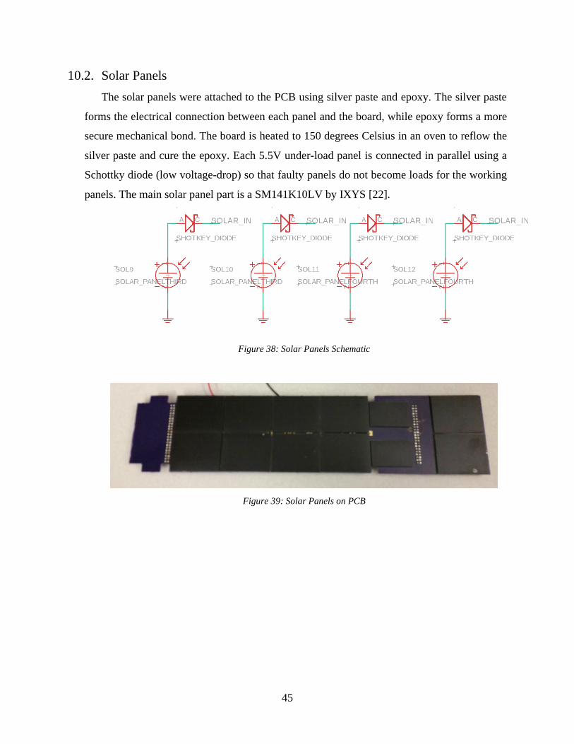
10.2. Solar Panels
The solar panels were attached to the PCB using silver paste and epoxy. The silver paste
forms the electrical connection between each panel and the board, while epoxy forms a more
secure mechanical bond. The board is heated to 150 degrees Celsius in an oven to reflow the
silver paste and cure the epoxy. Each 5.5V under-load panel is connected in parallel using a
Schottky diode (low voltage-drop) so that faulty panels do not become loads for the working
panels. The main solar panel part is a SM141K10LV by IXYS [22].
Figure 38: Solar Panels Schematic
Figure 39: Solar Panels on PCB

46
10.3. Maximum Power Point Controller
In order to maximize the power obtained from the panels irrespective of the level of
illumination a maximum power point tracking (MPPT) algorithm is being used. The LTC4162-
L chip can manage most of it automatically along with providing features to charge lithium ion
batteries when the panels are generating plenty of power as well as isolating them from the
power path when they are not generating power [23]. The part can be adjusted through I2C
communication and provide additional feedback information, but it is intended to be useful in
the default configuration. The IC provides the appropriate power source to the DC-DC
converters, based on how much power the solar panels are generating, the approximate battery
charge level, and instantaneous load. This power source is used to generate the main power
rails. The schematic below shows the main circuitry that connects the MPPT IC to the solar
panel input, battery out / dc-dc in, and 3.7 V battery pack input/output.
Figure 40: Power Controller Schematic

47
10.4. Lithium Ion Batteries
The rechargeable 3.7 lithium ion 18650 batteries are common off-the-shelf parts used in
the system to provide power when there is no sunlight illuminating that side of the Cubesat.
Each battery has a resettable positive temperature coefficient (PTC) fuse in series with its
positive terminal to protect itself from drawing too much current (shorting) and isolate it from
the rest of the system should the battery fail. Each power board is designed to have two batteries
attach to it. With some modifications, in future designs the batteries can be placed on the inside
section of the power board to be tightly integrated into the Cubesat platform as shown in the
image below.
Figure 41: A Cutaway View of The Side Power Board Being Mounted
Batteries

48
10.5. Power Distribution
The 5V and 3.3V power rails are shared amongst all four side power boards. Currently, the
5V powers only the Pi board dc-dc converter, while the 3.3V supply powers all sensors. The
5V rail is only connected to the computer interface board though it also passes through unused
to the top electronics board. The 3.3V supply connects to the sensors at the bottom and top
boards.
10.6. I2C Connections
The computer interface board multiplexed I2C lines connect to the bottom electronic board
sensors via the power board. This reduces the need for additional wiring and takes advantage
of the already connected power board.

49
11. pH Sensor Research
11.1. General pH Information and Existing Sensors
pH stands for the power of hydrogen and is the measurement of the concentration of
hydrogen ions, H+ / protons, in a solution. The solution is typically water-based and is
classified as acidic or basic relative to a neutral value. The usual range is between 0-14 pH
with 7 being the neutral value. There are several different types of pH sensors that are used to
measure the solution’s pH, the most common being a glass electrode. This working electrode
has a special glass membrane that is sensitive to the H+ ions and a potential voltage value is
taken usually with respect to a silver silver-chloride reference electrode. The voltage
measurements are taken with very high impedance due to the high impedance of the specialized
glass membrane itself. In general, the glass electrodes are all-in-one units, where the reference
electrode is included, and they are inexpensive to buy and acquire. They are typically very
large (to be used in beakers), need to be calibrated daily when used, and can degrade over time.
The glass makes the probe fairly fragile and hard to integrate into the small plant chambers.
Another type of pH sensor that is more robust and is typically smaller than the glass
electrode is the ion-sensitive field-effect transistor (ISFET). This transistor is gate sensitive to
H+ ions and will generate a measurable voltage potential. ISFETs have a similar structure to
MOSFET transistor types, and one type of gate material used is silicon dioxide. It is typical to
use an ISFET pH sensor when measuring food products since there is a high risk of
contamination than when using other sensors. Unfortunately, they still need a standard
reference electrode and are relatively hard to acquire at the time of writing. One portable ISFET
pH meter was tested with pH buffers to prove that they could be potentially used in the future.
An iridium oxide layer on a metal surface can also be used as the active pH electrode. The
oxide layer, typically IO2, is sensitive to the protons and can be made via electrodeposition of
an iridium oxide solution onto various metals and by thermally oxidizing iridium wire [24]
[25]. Both of these methods were applied and tested.
The electrodeposition iridium oxide solution did get appropriately applied to stainless steel
wire substrate using a potentiostat and could measure pH between various buffers, but had a
significant 180+ mV drift over a period of several days. Applying a nafion coating to try and
prevent the probe from degrading did not help.

50
The thermally oxidized iridium wire pH sensor could also sense pH but had a similar drift
error. It was created by cooking the thin iridium wire in a lithium salt at 825 degrees Celsius
for several hours and then cleaning it.
The official way of measuring the pH of soil involves taking a soil sample, making a slurry
out of it, and using a glass electrode to measure the pH in the solution. For the Cubesat project
and the payload goals, this method is impossible to perform so the other methods were
researched and experimented with. More work would have to be performed in order to get a
working miniature pH sensor solution for within the soil. Future design solutions could impact
problems beyond its original intent. A compact soil pH sensor developed for the plant
chambers can have positive effects when used in other scenarios, like smarter farming or
collecting data in an aquatic environment.
Figure 42: A Silver/Silver-Chloride Reference Electrode
Figure 43: Sealed Reference Electrode (top) and Electrodeposited Active Electrode (bottom)

51
Figure 44: A Thermally Oxidized Iridium Wire
Figure 45: pH Buffers
11.2. pH Measurement Goal
The goal of the crafted pH sensors was to measure the pH value via a calibratable voltage
potential between both the working and reference electrodes. The potential should have a slope
of about -59 mV per pH. The electrodes needed to be small to fit within the compacted soil
and the potential should not drift over time when measuring the same value (which can be
tested using collecting readings over an extended period of time). The refence electrode should
hold up to the long-intended measuring period of eight weeks.

52
12. Tests, Results, and Discussions
Tests were conducted on the sealing effectiveness of the mechanical Cubesat plus chamber
structure, individually on the electronics boards, and a few tests with the whole design
assembled as one unit.
12.1. Equipment Used
Some of the major equipment used in the testing includes a benchtop four channel
oscilloscope, multiple digital multimeters, and DC power supplies. The multimeters were used
to check for proper continuity and no shorts across all circuits after assembly (soldering),
voltage levels of the converters, and current draw of the major power elements. The
oscilloscope was used to verify the proper UART, I2C, and camera digital communications
between the computer and the corresponding sensors after programming logic based on the
various data sheets. The power supplies were used to provide the main DC rails and some
intermediary rails (such as the camera power rails) depending on the test. Other equipment
used includes pressure gauge, lights, and pH buffers and meters as described in other sections.
12.2. Mechanical Sealing Check
The scientific Cubesat payload chambers have to be all sealed air tight so that they retain
their initial atmosphere, which gives them an individual closed ecological system with the
exception of adding energy from the grow lights. The mechanical design was built around how
to create a seal and as described in the previous Mechanical Structure Supporting the Scientific
Payload section, it involves using O-rings, gaskets, and epoxy
During the mechanical design process a test was conducted using aluminum plate
substitutes for the top and bottom PCBs in order to ensure sealing was occurring for an
extended period of time. In order to simulate retaining atmospheric pressure in each of the
chambers with respect to a vacuum on the outside, the pressure in each chamber was held at
two atmospheric pressure (atm) for several weeks with about a one pound-per-square-inch (psi)
loss. The top electronics board was epoxied and tested by applying the pressure gauge plate to
the bottom and it had the same results of only losing about one psi.

53
Figure 46: Pressure Gauge and Aluminum Mounting Plate Used
Figure 47: Sealing the Top Circuit Board with Epoxy

54
12.3. Top Electronics Board Test
The top electronics board was tested to ensure that all of the sensors, cameras, and LEDs
could be monitored and controlled for each chamber. A Pi computer board was connected to
each chamber connections section with jumpers and wires. The I2C communications protocol
was used to retrieve room temperature values from each IC, and the RGB LEDs were turned
on with various brightness intensities for several colors. The camera picture capture code was
run and it turns on the white LED to capture a picture, and then it turns off the white LED and
turns on the IR LED to save a new picture. Within a dark environment, it was shown that the
camera was sensitive to visible and infrared light spectrums. The UART CO2 sensor was
interfaced with to sense usual levels of around 350 ppm. Each chamber electronics was
individually tested by changing which chamber the Pi was connected to.
12.4. Interface Board
The interface board was tested to ensure that one raspberry Pi computer could communicate
with all sensors, LEDs, and cameras in each of the four chambers. After an initial hardware
setup and modified software that included adding multiplexor configuration and camera power
converter enable switches, one computer was able to switch between each chamber to log
sensor data and control the LEDs and camera.
12.5. Ground Based Plant Testing with Top Chamber Board
Fast plants and bean plants were the first ground based Cubesat payload testing. Soil and
two seeds of one of the plants were placed inside each of the chambers, and each soil was given
a water level based upon past research presented in the RIT college of science paper
Development of CubeSat Controls for Future Low-Gravity Rhizospheric. The main goal was
to determine if the Pi computer could log the different sensor information from the top
electronic board and collect images while the plants effectively grew over the course of weeks
while in the sealed chambers. The red and blue grow lights were put on an 18-hour on, 6-hour
off daily cycle and pictures were saved every hour. After several initial failed attempts while
the water levels and grow light intensity levels were adjusted, plants did end up growing in the
sealed chambers. The plants were eventually extracted out of the Cubesat to weigh their
biomass.

55
The Pi computer was connected via ethernet to the network in order to take advantage of
the remote software capabilities
Figure 48: Cubesat with Top Electronics Initial Ground Based Testing
Figure 49: Inside Chamber White Light Plant Picture Time

56
Figure 50: Top Down Look of Plants in Chambers
Figure 51: Plant Extraction at End of Experiment
Bean Plant Fast Plant
Fast Plants
Bean Plant

57
The bean plant was really able to grow and fill up the chamber space when compared to
the fast plants which shows that only certain plant types can grow in the limited chamber space
choosing the right type for future scientific experiments is critical to the success. Many more
ground-based experiments need to be conducted in the future and it would be important to
determine what conditions can be modified to ensure healthier plants, unlike the fast plant that
fell over when not supported by the chamber walls.
12.6. Side Electronics Board Testing
The side electronics board was tested to ensure that sunlight, incandescent light, and
halogen light would create power on the solar panels and the two main voltage rails, 3.3V and
5V would be generated. When batteries were added in to the circuit, the solar panels could
either be illuminated or be in the dark and the power rails would still exist. Unfortunately, the
tolerance for the batteries to be placed in their designed positions was too tight and they could
not be mounted as the figure below shows. The mounting solution was varied (and even spot
welded to the batteries) to determine if it could be fixed with an easy change with no success.
Potentially, multiple 14500 size lithium ion rechargeable batteries can be used to fit in the
future design if it is determined that the lower capacity trade off makes sense.
The I2C communications between the computer interface board and the bottom electronics
board did provide a good connection between the Pi computer and the bottom ADCs and
temperature sensor. This allows for the computer to record bottom chamber sensor information
when the side electronic boards are mounted. In general, the four-layer side panel boards
provide plenty of ways to electrically connect the electronics in different regions of the Cubesat
without using wiring harnesses.
The mounting solution of the side panel boards went through several designs and when the
next iteration of all the electronics boards occurs, the boards should be mounted in a way that
they push onto each side (and potentially screwed into the side rails).

58
Figure 52: Battery in Mounts on Side PCB
Figure 53: Side Solar Panel Power Boards Mounted on Cubesat
The DC-DC buck-boost converters used for the main power rails after the MPPT chip
power output should be changed so that they can supply more current for the computer and
sensors and be more easily setup in parallel. After several tests, the resistive load sharing
circuitry added to the power rails caused more problems than it solved.

59
12.7. Power Used and Budget
A general power usage breakdown and total usage within the Cubesat system is shown in
the table below. The listed power values consumed by each item is a calculated maximum.
Since either the grow lights or one camera (cycled) is running at a time, they are listed as one
item with the grow lights dictating the maximum power. There is no current budget allocated
for charging the batteries unless the grow lights are shut off and possibly the Pi computer from
a future master microcontroller as mentioned in a subsection of the Future Work section. The
grow lights can remain in their current state regardless of the Pi being powered. The total power
budget stems from one active power side power electronics board being illuminated which is
a current limitation.
In general, this is not the ideal power budget to be working from since there is no remaining
power and no accountable tolerance. More work on a detailed power plan is necessary as a
more complete system design is described. Design choices kept fluctuating during the
engineering process which added complications in determining what active components could
be used until the solar panel / side electronics power board was designed so an effort was made
to use lower-power sensors and fewer computers when multiple options were considered.
The Pi computer power value stems from a Pi 3B+ running at a useable idle, or a Pi Zero
running one core at typical levels. The grow light LED power calculations assume the
previously used 18 mA per diode.
Table 1: Power Budget Calculations
Item Max Power (Watts) Quantity Running Budget (Watts)
Big Solar Panel +0.3 10 +3.0
Small Solar Panel +0.05 2 +3.1
Pi Computer -1.0 1 +2.1
All Grow Lights or Cameras -1.5 16 LEDs or
1 Camera
+0.6
Chamber Sensors -0.5 4 +0.1
Other Active ICs -0.1 N/A 0.0

60
13. Future Work
Other design elements were analyzed into but not fully implemented.
13.1. Radio Communications
Master Microcontroller Board
A low-powered, radiation resistant (rad-hard) TI MSP430 based microcontroller was
considered for a master computer and the raspberry Pi computer would be a slave device. This
microcontroller would be useful for controlling the two required amateur radio bands, 2m and
70cm (which can be used for non-commercial purposes). The master microcontroller would
manage communications with a base station (potentially switching bands / sub-frequencies for
higher bandwidth or other conflict) and potentially transfer information from and to the Pi
computer using a serial UART-like connection.
Potential Radio Chip
A binary FSK communication at the required bands could be useful and possibly could be
done using one Silicon Labs Si446x chip [26]. Input / output antenna switches could be added
to enable half-duplex communications on either band based on chip register configurations and
appropriate external passive filtering.
A Radio Antenna for Both Bands
A collapsible monopole radio antenna that met the 2m quarter wavelength and was a
reasonable fraction of the 70cm band was created in CAD using off the shelf component metals
and springs to demonstrate how it might be added to the Cubesat design. A picture of the
collapsed version, attached to a bottom plate, is shown below. This is a simple antenna that
would need impedance matching and testing to prove its usefulness.

61
Figure 54: Monopole antenna CAD Mock-up
13.2. Attitude Determination and Control System
An ADCS is only necessary for the space version of the Cubesat, since it would not provide
much control for the high-altitude balloon version. Space has been allotted at the top of the
Cubesat to make room for a current off-the shelf commercial ADCS, though there are many
designs of ADCSs, some are published by other student / academic groups. When an ADCS is
not necessary to be on the Cubesat platform, a different system could occupy the space to
provide a connection to the balloon, hold a parachute, and capture and relay GPS signals. This
can be done using an automatic packet reporting systems (ARPS) and off-the shelf modules
that can work independently with minimal setup before connecting to the wide-coverage
network.

62
13.3. Sensor Additions
Adding more sensors to the chambers and Cubesat in general can possibly provide more
relevant information. It would be useful to have an in-chamber radiation sensor that can detect
various background radiation built up over time such as TID. This could be useful to record
instead of simply speculating how much radiation was impacting the plant growth and could
be useful in comparison to tests run on the ground or when conducting tests on the high-altitude
balloon. Potentially, DNA dosimeters and/or chemical actinometers might be used in the
chambers directly after many design and requirement considerations. Device form-factor and
power consumption concerns might limit their inclusion.
Having multiple external temperature sensors could be useful in determining an effective
thermal profile of the Cubesat at key sections of the mostly aluminum body as it orbits the
earth. The data could then be used in developing a future, more temperature managed friendly
Cubesat, which might allow the plants to grow within a better controlled temperature range.
13.4. Future Tests
Another full system ground test should be conducted using all of the sensors including the
soil moisture and a finalized soil pH sensor. The test would include running the Cubesat off of
artificial light that illuminates the solar panels to create the necessary power to run the
electronic boards, sensors, and charge the batteries.
During the full system tests, more thorough thermal analysis needs to be run on the system.
Ideally this would be conducted in a vacuum chamber to ensure that the sealed plant chambers
maintain pressure, and stay within acceptable temperature values as stated by the requirements.
Thermal transfers would be restricted to radiation and conduction outside of the chambers
which matches real-flight cases. Applying a thermal radiation input that is similar to the power
generated by the sun for the given surface area of the Cubesat would be ideal. There is expected
to be about 55 watts of power radiated by the sun towards one side of the 3U Cubesat based
on the approximate 1.3 kW/m2 of power from the sun around LEO. Using an accurate orbit
sun equivalent profile, thermals can be tested before a flight test ever occurs.
The grow light LEDs can be used to possibly help manage the air temperature within the
atmosphere of the chamber since they draw a lot of power. Determining appropriate energy /
light intensities vs power consumption.

63
Vibration testing of the Cubesat should be conducted to determine what parts of the
mechanical structure should be joined differently, such as using a different form of screws and
using Loctite on the threads. The Cubesat should ideally be tested to EM radiation, and possibly
shielded from incoming radiation but no plan has currently been created to test for it.
While all of the above described tests are important to run, more individualized tests can
be conducted for each electronics board. This testing can qualify the electronic boards from
one version to the other to determine what has improved versus degraded and what has met
stricter, more detailed engineering requirements. Quality testing performed at various steps
along the engineering process comes from a solid workflow that normally leads to success.

64
14. Conclusions
The goal of the project was to design and build a Cubesat that will enable the scientific
goal of creating optimal microbiomes to support plant growth in space. Once the scope of the
project was reduced to manageable parameters, an initial design was constructed and tested
which should be expanded upon in the future.
Four electronics board designs were created of the likely seven to eight board designs
needed in the future to finish a flyable Cubesat. The four boards created and tested can all be
improved in future iterations while the other minimum three boards would include necessary
features. These features include a radiation tolerant master microcontroller, radio
communications, and an ADCS management system.
The mechanical structure is easily changeable due to the simplicity of the construction of
each individual part. It would be straightforward to add more mounting holes to the rails in
order to provide more structure of the side PCBs provide lots of potential ways to mount both
the communications antenna system and the future, potentially off-the-shelf ADCS. Sealing
the chambers with the O-rings, gaskets, and epoxy combination has been proven to be
effective.
Individual testing of the electronics fairs well, but when testing the Cubesat as a whole it
begins to fail when under heavy power draw. The power supplied from the solar panels,
batteries, and simulated power supply batteries, cannot keep up when the multiple dc-dc 5V
converters are in parallel, however when the converters were circumvented, the computer,
other electronics, and the sensors acted as intended.
Most of the major Cubesat requirements have been designed and met. Currently the
Cubesat weighs less than 4kg, leaving enough margin for the addition of deployment switches,
ADCS, RF transceiver and associated antenna, and the master controller board. The scientific
payload requirements have been also followed and designed too.
In general, this project and design provide a good start for future RIT student missions
pertaining to Cubesats. It is worth mentioning that the Cubesat has several single points of
failure that could be reduced in future versions. These future Cubesat platforms may reuse the
bio-experimental chambers and engineering principles applied here.
65
15. References
[1] "P13271: AMSAT," [Online]. Available: http://edge.rit.edu/edge/P13271/public/Home.
[2] "P16102: RIT-SPEX Structure," [Online]. Available: http://edge.rit.edu/edge/P16102/public/Home.
[3] "P16103: RIT-SPEX Vibration Test Rig," [Online]. Available:
http://edge.rit.edu/edge/P16103/public/Home.
[4] "P18101: CubeSat Solar Sail," [Online]. Available: http://edge.rit.edu/edge/P18101/public/Home.
[5] "P19101: CubeSat Solar Sail," [Online]. Available: http://edge.rit.edu/edge/P19101/public/Home.
[6] "P19104: HABIP-BioX," [Online]. Available: http://edge.rit.edu/edge/P19104/public/Home.
[7] Cubesat.org, "Cubesat Design Specification," [Online]. Available:
https://static1.squarespace.com/static/5418c831e4b0fa4ecac1bacd/t/
56e9b62337013b6c063a655a/1458157095454/cds_rev13_final2.pdf.
[8] "Materials for use in vacuum," [Online]. Available:
https://en.wikipedia.org/wiki/Materials_for_use_in_vacuum.
[9] Analog Devices, "ADT7420 Datasheet," [Online]. Available:
https://www.analog.com/media/en/technical-documentation/data-sheets/ADT7420.pdf.
[10] "MS5607-02BA03," [Online]. Available:
https://www.te.com/commerce/DocumentDelivery/DDEController?
Action=showdoc&DocId=Data+Sheet%7FMS5607-02BA03%7FB2%7Fpdf%7FEnglish%
7FENG_DS_MS5607-02BA03_B2.pdf%7FCAT-BLPS0035.
[11] Sensirion, "SHT3x-DIS Datasheet," [Online]. Available:
https://www.sensirion.com/fileadmin/user_upload/customers/sensirion/
Dokumente/0_Datasheets/Humidity/ Sensirion_Humidity_Sensors_SHT3x_Datasheet_digital.pdf.
[12] Gas Sensing Solutions, "COZIR™ LP Datasheet," [Online]. Available:
http://www.gassensor.ru/data/files/carbon_dioxide/gss-cozir-lp-co2-sensor-datasheet.pdf.
[13] Kingbright, "WP154A4SUREQBFZGC Datasheet," [Online]. Available:
http://www.kingbrightusa.com/images/catalog/SPEC/WP154A4SUREQBFZGC.pdf.
[14] Raspberry Pi, "Buy Pi NoIR Camera V2 Official," [Online]. Available:
https://www.raspberrypi.org/products/pi-noir-camera-v2/.

66
[15] "Pi Camera v2 Schematic," [Online]. Available:
https://www.raspberrypi.org/documentation/hardware/camera/
schematics/rpi_SCH_Camera2_2p1.pdf.
[16] "LUXEON 3014," [Online]. Available: https://www.lumileds.com/uploads/459/DS208-pdf.
[17] Microchip, "Tiny Serial Digital Thermal Sensor," [Online]. Available:
http://ww1.microchip.com/downloads/en/devicedoc/21462d.pdf.
[18] DF Robot, "Capacitive Soil Moisture Sensor," [Online]. Available:
https://wiki.dfrobot.com/Capacitive_Soil_Moisture_Sensor_SKU_SEN0193.
[19] D. P. Violette, "Arduino/Raspberry Pi: Hobbyist Hardware and Radiation Total Dose Degradation,"
NASA, September 2014. [Online]. Available:
https://nepp.nasa.gov/workshops/eeesmallmissions/talks/11%20-%20THUR/
1430%20-%202014-561-%20Violette-Final-Pres-EEE-TN17486%20v2.pdf.
[20] O. Gutiérrez, M. Prieto, A. Sánchez-Reyes and A. Gómez, "TID characterization of COTS parts
using Radiotherapy Linear Accelerators," The Institute of Electronics, Information and
Communication Engineers, March 2019. [Online]. Available:
https://www.jstage.jst.go.jp/article/elex/advpub/0/advpub_16.20190077/_pdf/-char/en.
[21] "Load Sharing Concepts: Implementation for Large-Signal," [Online]. Available:
http://www.ti.com/lit/an/sboa127/sboa127.pdf.
[22] Ixys, "SM141K10LV Datasheet," [Online]. Available:
http://ixapps.ixys.com/DataSheet/SM141K10LV.pdf.
[23] "LTC4162-L Datasheet," [Online]. Available: https://www.analog.com/media/en/technical-
documentation/data-sheets/LTC4162-L.pdf.
[24] C. C. Mayorga Martinez, R. E. Madrid and C. J. Felice, "A pH Sensor Based on a Stainless Steel
Electrode Electrodeposited With Iridium Oxide," IEEE Transactions on Education, vol. 52, no. 1,
pp. 133-136, 2009.
[25] C. Ratanaporncharoen, M. Tabata, N. Watanagool, T. Goda, A. Matsumoto, M. Sriyudthsak and Y.
Miyahara, "Characterization and Optimization of Thermally Grown Iridium Oxide and Its
Application to pH Sensors," Sensors and Materials, vol. 30, no. 5, pp. 1175-1185, 2018.
[26] Silicon Labs, "Si446x Datasheet," [Online]. Available:
https://www.silabs.com/documents/public/data-sheets/Si4464-63-61-60.pdf.