a 28ghz, 4-channel phase adjustable power amplifier ic … · a 28ghz, 4-channel phase adjustable...
TRANSCRIPT
A 28GHz, 4-channel Phase Adjustable Power Amplifier IC for
5G front-ends
Stuart Glynn and Liam Devlin
Plextek RF Integration, London Road, Great Chesterford, Essex, CB10 1NY, UK;
Abstract
5G communications promises to offer the user the perception of near infinite capacity. This will
require a step change in data rates, which will be facilitated by a move to higher transmission
frequencies where wider bandwidths are more readily available. New innovative components will be
required to allow the design of suitable hardware, such as the 4-channel 28GHz (27 to 29.5GHz)
phase adjustable Power Amplifier (PA) IC described here. Each channel of the IC includes a PA with
an integral 4-bit, digitally controlled phase shifter offering a compact means of providing beam
steering as an integral part of the PA. The output power capability of each channel is +30dBm (at
1dB compression) with an IP3 of +38dBm. The phase shifters include TTL compatible control and
have an rms phase error of 2.3°.
Introduction
An enormous amount of research effort is currently being devoted to developing 5G technology with
the aim of roll out by the year 2020. The details of the 5G standard are yet to be defined but a
common vision for this new standard is that as well as providing much higher data rates it must also
allow for extremely low latency (less than one millisecond) and uniform coverage over a wide area.
As well as providing improved performance for existing applications, for example allowing the
download of several HD movies in a second, the technology will enable and encourage the
development of new markets, technologies and applications.
Although there is still much debate about the precise form that 5G will take, there is a degree of
consensus that the standard will frequently require large chunks of contiguous spectrum. This can
only be found by utilizing frequencies much higher than the current cellular frequencies of around
3GHz and below. Therefore, as well as the use of current cellular frequencies, a key component of
the new 5G radio interface will be the use of mm-wave frequencies where there is greater spectral
availability.
Until recently mm-waves have been viewed as a rather inappropriate choice for mobile applications
due to their unfavourable propagation characteristics. However, recent research, involving extensive
propagation measurements at several mm-wave frequencies around metropolitan areas in both the
United States [1] and South Korea, has shown that the issues can be addressed and overcome. Such
research included the investigation of more sophisticated antenna schemes employing phased
arrays of antennas to optimise the transmitted and received beams at both the base-station and the
mobile device. The fact that wavelengths are small at mm-wave frequencies allows such arrays to be
incorporated into a small mobile form factor. It also allows the implementation of compact base-
stations which will facilitate regular deployment around metropolitan areas.

Bands within 27 to 29.5GHz are strong candidates for the new 5G radio interface and much of the
research undertaken to date has been conducted at around 28GHz [2]. This paper describes the
design of a 4-channel transmitter IC with each channel containing a PA with integral 4-bit phase
shifter. The IC is designed using a commercially available 0.15µm GaAs pHEMT process and is
intended to be housed in a low cost SMT package suitable for volume production.
28GHz 5G Transmit RF Front End Architecture
The architecture of an RF Front-End (RFFE) using the 28GHz transmit IC is depicted in Figure 1 below.
It shows a 4 element antenna array, where each element is driven by one of four parallel phase
adjustable power amplifiers. It is likely that some degree of filtering would be implemented
immediately after each power amplifier for harmonic rejection and suppression of receive band
noise and unwanted spurious outputs. The 4 channels are each driven in-phase from a common RF
input via a 4-way splitter.
Figure 1: Architecture of the 4-channel transmitter IC
4 Parallel, Phase Adjustable, PAs in a
Single SMT Package
ɸ
ɸ
ɸ
ɸ
4 Parallel
Transmit
Filters
4 Element
Antenna
Array
Phase Adjust
Phase Adjust
Phase Adjust
Phase Adjust
5G
Transceiver
CH1
CH2
CH3
CH4
RF IP 1 to 4 In-
Phase Power
Splitter
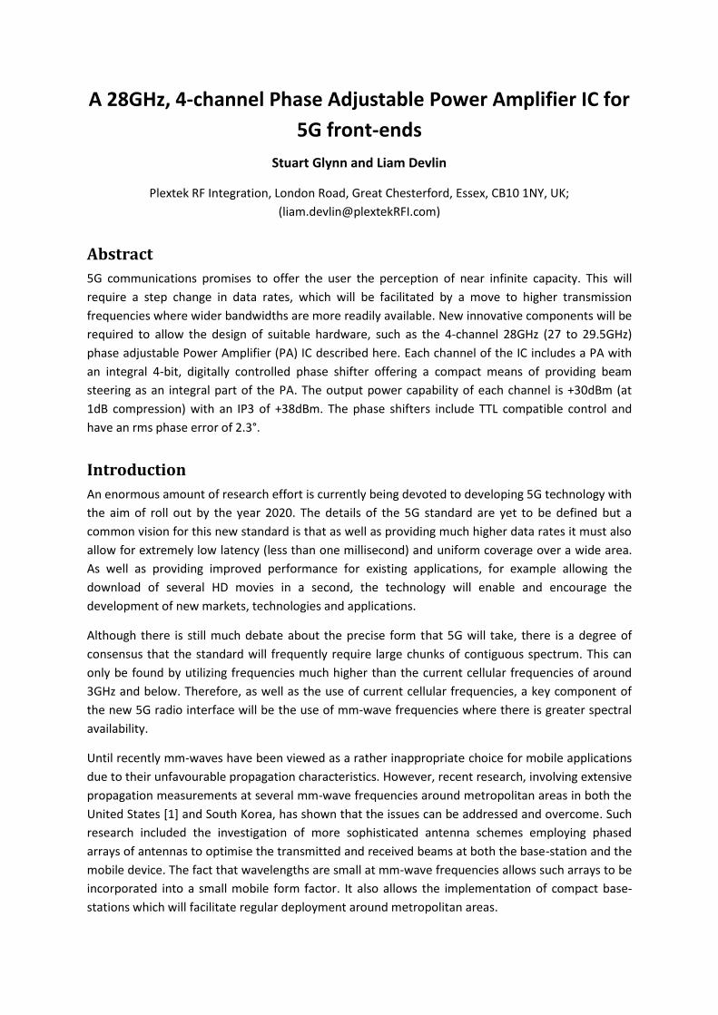
The IC itself is a 4-channel part but if a particular architecture required a higher number of elements
in the antenna array, say 16, then multiple ICs could simply be used in parallel.
A layout plot of one channel of the transmitter IC is shown in Figure 2; this is a stand-alone test-chip
– the transmitter IC itself comprises 4 separate channels with an in-phase splitter at the input. The
test chip measures 3.8mm x 1.84mm.
The PA output (to the right of the layout image) comprises 4 power combined transistors, driven
from 2 transistors of the same size. The 4-bit phase shifter is positioned before this with an input
stage of amplification that is a modified version of the 2 transistor driver stage. The drain supplies
for the power amplifier are Vd1, Vd2 and Vd3 and they are nominally set to +6V. Vg1 sets the
quiescent bias current in the first stage and Vg23 sets the quiescent bias current in the second and
third stages.
Figure 2: Layout plot of one channel of the transmitter IC
The phase state of each bit of the integrated phase shifter is controlled by a single-ended TTL
compatible control line. All of the control logic required to shift the levels to those needed for the
phase shifter bits is included on-chip. The truth table for the integrated phase shifter is shown in
Table 1 below.
RF input RF output
Vg1 Vd1 Bit0 Bit1 +5V Bit2 Bit3
Vg23 Vd2 Vd3

Bit0 Bit1 Bit2 Bit3 Relative Phase Shift (nominal)
0V 0V 0V 0V 0°
+5V 0V 0V 0V 22.5°
0V +5V 0V 0V 45°
+5V +5V 0V 0V 67.5°
0V 0V +5V 0V 90°
+5V 0V +5V 0V 112.5°
0V +5V +5V 0V 135°
+5V +5V +5V 0V 157.5°
0V 0V 0V +5V 180°
+5V 0V 0V +5V 202.5°
0V +5V 0V +5V 225°
+5V +5V 0V +5V 247.5°
0V 0V +5V +5V 270°
+5V 0V +5V +5V 292.5°
0V +5V +5V +5V 315°
+5V +5V +5V +5V 337.5°
Table 1: Truth table for phase setting of each channel
Single Channel Performance
The performance plots presented below are at room temperature, nominal bias across the
frequency range 26 to 30GHz.
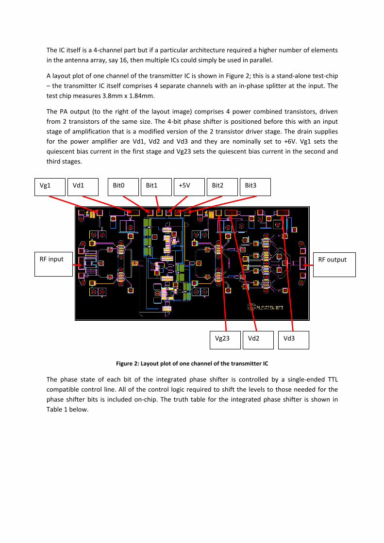
The 4-bit phase shifter is based on a switched high-pass/low-pass filter topology [3]; it allows the
insertion phase of each channel to be independently set with 22.5° resolution. The most significant
bit (180°) uses two Single Pole Double Throw (SPDT) switches to route the RF signal through either a
low pass or a high pass filter, as depicted in Figure 3. The high pass filter exhibits a phase advance
compared to the low pass filter with the phase difference being relatively constant over a reasonable
bandwidth. Optimisation of the component values is required to obtain the desired phase difference
with an acceptable amplitude difference. The lower order bits make use of re-configurable phase
shifter bits, such as that depicted in Figure 4, which offers the benefit of lower insertion loss.
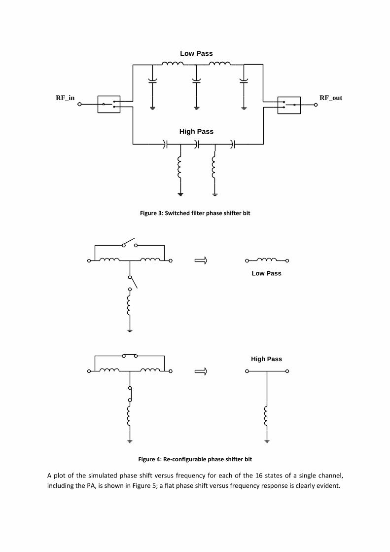
Figure 3: Switched filter phase shifter bit
Figure 4: Re-configurable phase shifter bit
A plot of the simulated phase shift versus frequency for each of the 16 states of a single channel,
including the PA, is shown in Figure 5; a flat phase shift versus frequency response is clearly evident.
RF_out
Low Pass
High Pass
RF_in
Low Pass
High Pass
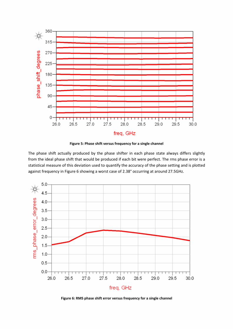
Figure 5: Phase shift versus frequency for a single channel
The phase shift actually produced by the phase shifter in each phase state always differs slightly
from the ideal phase shift that would be produced if each bit were perfect. The rms phase error is a
statistical measure of this deviation used to quantify the accuracy of the phase setting and is plotted
against frequency in Figure 6 showing a worst case of 2.38° occurring at around 27.5GHz.
Figure 6: RMS phase shift error versus frequency for a single channel
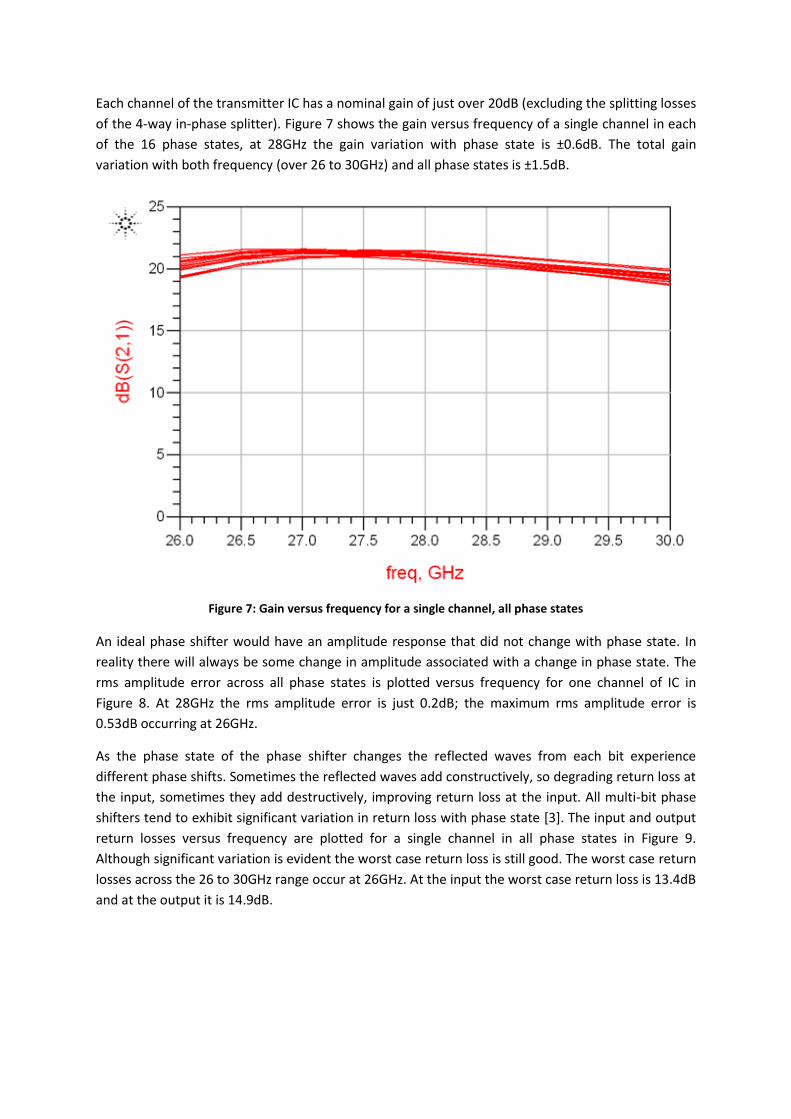
Each channel of the transmitter IC has a nominal gain of just over 20dB (excluding the splitting losses
of the 4-way in-phase splitter). Figure 7 shows the gain versus frequency of a single channel in each
of the 16 phase states, at 28GHz the gain variation with phase state is ±0.6dB. The total gain
variation with both frequency (over 26 to 30GHz) and all phase states is ±1.5dB.
Figure 7: Gain versus frequency for a single channel, all phase states
An ideal phase shifter would have an amplitude response that did not change with phase state. In
reality there will always be some change in amplitude associated with a change in phase state. The
rms amplitude error across all phase states is plotted versus frequency for one channel of IC in
Figure 8. At 28GHz the rms amplitude error is just 0.2dB; the maximum rms amplitude error is
0.53dB occurring at 26GHz.
As the phase state of the phase shifter changes the reflected waves from each bit experience
different phase shifts. Sometimes the reflected waves add constructively, so degrading return loss at
the input, sometimes they add destructively, improving return loss at the input. All multi-bit phase
shifters tend to exhibit significant variation in return loss with phase state [3]. The input and output
return losses versus frequency are plotted for a single channel in all phase states in Figure 9.
Although significant variation is evident the worst case return loss is still good. The worst case return
losses across the 26 to 30GHz range occur at 26GHz. At the input the worst case return loss is 13.4dB
and at the output it is 14.9dB.
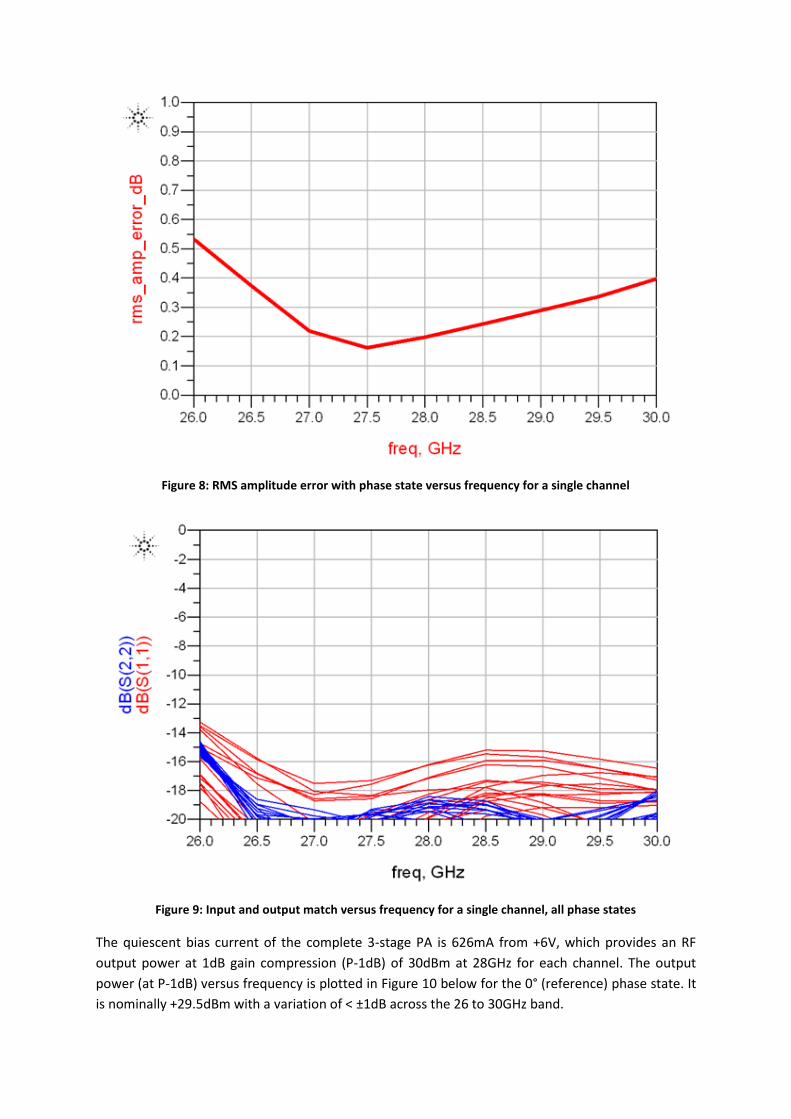
Figure 8: RMS amplitude error with phase state versus frequency for a single channel
Figure 9: Input and output match versus frequency for a single channel, all phase states
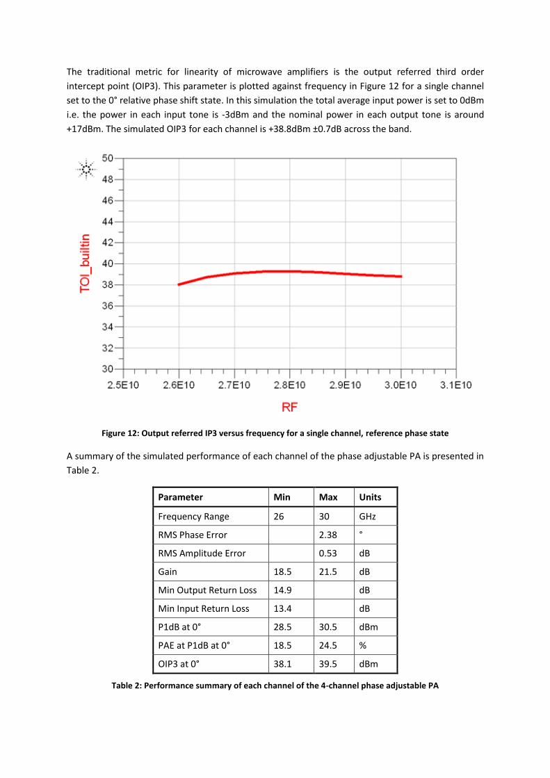
The quiescent bias current of the complete 3-stage PA is 626mA from +6V, which provides an RF
output power at 1dB gain compression (P-1dB) of 30dBm at 28GHz for each channel. The output
power (at P-1dB) versus frequency is plotted in Figure 10 below for the 0° (reference) phase state. It
is nominally +29.5dBm with a variation of < ±1dB across the 26 to 30GHz band.
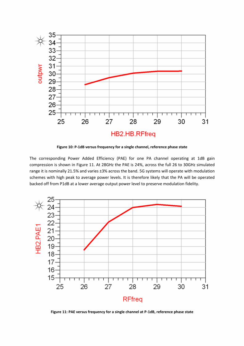
Figure 10: P-1dB versus frequency for a single channel, reference phase state
The corresponding Power Added Efficiency (PAE) for one PA channel operating at 1dB gain
compression is shown in Figure 11. At 28GHz the PAE is 24%, across the full 26 to 30GHz simulated
range it is nominally 21.5% and varies ±3% across the band. 5G systems will operate with modulation
schemes with high peak to average power levels. It is therefore likely that the PA will be operated
backed off from P1dB at a lower average output power level to preserve modulation fidelity.
Figure 11: PAE versus frequency for a single channel at P-1dB, reference phase state
The traditional metric for linearity of microwave amplifiers is the output referred third order
intercept point (OIP3). This parameter is plotted against frequency in Figure 12 for a single channel
set to the 0° relative phase shift state. In this simulation the total average input power is set to 0dBm
i.e. the power in each input tone is -3dBm and the nominal power in each output tone is around
+17dBm. The simulated OIP3 for each channel is +38.8dBm ±0.7dB across the band.
Figure 12: Output referred IP3 versus frequency for a single channel, reference phase state
A summary of the simulated performance of each channel of the phase adjustable PA is presented in
Table 2.
Parameter Min Max Units
Frequency Range 26 30 GHz
RMS Phase Error 2.38 °
RMS Amplitude Error 0.53 dB
Gain 18.5 21.5 dB
Min Output Return Loss 14.9 dB
Min Input Return Loss 13.4 dB
P1dB at 0° 28.5 30.5 dBm
PAE at P1dB at 0° 18.5 24.5 %
OIP3 at 0° 38.1 39.5 dBm
Table 2: Performance summary of each channel of the 4-channel phase adjustable PA
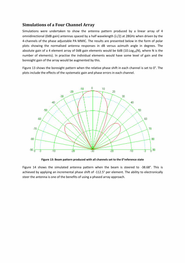
Simulations of a Four Channel Array
Simulations were undertaken to show the antenna pattern produced by a linear array of 4
omnidirectional (0dB gain) antennas spaced by a half wavelength (/2) at 28GHz when driven by the
4-channels of the phase adjustable PA MMIC. The results are presented below in the form of polar
plots showing the normalised antenna responses in dB versus azimuth angle in degrees. The
absolute gain of a 4 element array of 0dB gain elements would be 6dB (10.Log10(N), where N is the
number of elements). In practise the individual elements would have some level of gain and the
boresight gain of the array would be augmented by this.
Figure 13 shows the boresight pattern when the relative phase shift in each channel is set to 0°. The
plots include the effects of the systematic gain and phase errors in each channel.
Figure 13: Beam pattern produced with all channels set to the 0°reference state
Figure 14 shows the simulated antenna pattern when the beam is steered to -38.68°. This is
achieved by applying an incremental phase shift of -112.5° per element. The ability to electronically
steer the antenna is one of the benefits of using a phased array approach.

Figure 14: Beam pattern produced with phase states of the 4 channels set to steer the beam to -38°
Concluding Remarks
This paper describes the design of a 4-channel 28GHz (27 to 29.5GHz), transmitter IC. Each channel
of the IC includes a power amplifier with an integral, independently controllable 4-bit digital phase
shifter. The IC is intended for use in the transmit chain of a 5G RF Front-End (RFFE) module in either
a mobile device or a base-station. It has been designed using a commercially available 0.15µm GaAs
pHEMT process and is suitable for assembly in to a single SMT package.
Details of the layout of a test chip for evaluating the performance of a single channel were
presented along with simulation results of key performance parameters including rms phase error,
rms amplitude error and OIP3. Antenna pattern simulations for four channels driving four elements
in a linear array were also given showing the potential for beam steering using the 4-channel MMIC.
It was noted that although this paper has focused on a four element array, the solution can be
extended to larger antenna arrays. For example if the number of elements in the antenna array was
16 then this would require four of the 4-channel phase adjustable power amplifiers in parallel.
References
[1] Theodore S. Rappaport, NYU Wireless, “Millimeter Wave Mobile Communications for 5G
Cellular: It Will Work!”, IEEE Access 30th May 2013
[2] Wonbin Hong, Samsung Electronics, “Design and Analysis of a Low-Profile 28GHz Beam
Steering Antenna Solution for Future 5G Cellular Applications”, IEEE MTT-S International,
June 2014
[3] Liam Devlin, “The Design of Integrated Switches and Phase Shifters”, Proceedings of the IEE
Tutorial Colloquium on “Design of RFICs and MMICs”, Wednesday 24th November 1999, pp
2/1-14