951-0 microproc fmbooks.mhprofessional.com/engineering/pdfs/mcfarland.pdf · the evolution of the...
TRANSCRIPT

Microprocessor Design
6x9 Technical / Microprocessor Design / McFarland /45951-0/ Front Matter
951-0 Microproc_FM 9/3/06 6:51 PM Page i

6x9 Technical / Microprocessor Design / McFarland /45951-0/ Front MatterBlind folio ii
951-0 Microproc_FM 9/3/06 6:51 PM Page ii

6x9 Technical / Microprocessor Design / McFarland /45951-0 / Front Matter
Microprocessor DesignA Practical Guide from Design Planning
to Manufacturing
Grant McFarland
McGraw-HillNew York Chicago San Francisco Lisbon London Madrid
Mexico City Milan New Delhi San Juan Seoul Singapore Sydney Toronto
951-0 Microproc_FM 9/3/06 6:51 PM Page iii
6x9 Technical / Microprocessor Design / McFarland /45951-0/ Front Matter
CIP Data is on file with the library of Congress
Copyright © 2006 by The McGraw-Hill Publishing Companies, Inc. Allrights reserved. Printed in the United States of America. Except as per-mitted under the United States Copyright Act of 1976, no part of this pub-lication may be reproduced or distributed in any form or by any means,or stored in a data base or retrieval system, without the prior written per-mission of the publisher.
1 2 3 4 5 6 7 8 9 0 DOC/DOC 0 1 9 8 7 6
ISBN 0-07-145951-0
The sponsoring editor for this book was Wendy Rinaldi and theproduction supervisor was David Zielonka. It was set in CenturySchoolbook by International Typesetting and Composition. The artdirector for the cover was Anthony Landi.
Printed and bound by RR Donnelley.
McGraw-Hill books are available at special quantity discounts to use aspremiums and sales promotions, or for use in corporate training pro-grams. For more information, please write to the Director of SpecialSales, McGraw-Hill Professional, Two Penn Plaza, New York, NY 10121-2298. Or contact your local bookstore.
Information contained in this work has been obtained by TheMcGraw-Hill Companies, Inc. (“McGraw-Hill”) from sourcesbelieved to be reliable. However, neither McGraw-Hill nor itsauthors guarantee the accuracy or completeness of any informa-tion published herein and neither McGraw-Hill nor its authorsshall be responsible for any errors, omissions, or damages aris-ing out of use of this information. This work is published with theunderstanding that McGraw-Hill and its authors are supplyinginformation but are not attempting to render engineering or otherprofessional services. If such services are required, the assistanceof an appropriate professional should be sought.
951-0 Microproc_FM 9/3/06 6:51 PM Page iv

6x9 Technical / Verilog Digital System Design / Navabi /44564-1 / Front Matter
To Elaine
951-0 Microproc_FM 9/3/06 6:51 PM Page v

6x9 Technical / Microprocessor Design / McFarland /45951-0/ Front MatterBlind folio vi
951-0 Microproc_FM 9/3/06 6:51 PM Page vi

vii
6x9 Technical / Verilog Digital System Design / Navabi /44564-1 / Front Matter
Brief Contents
Chapter 1. The Evolution of the Microprocessor 1
Chapter 2. Computer Components 37
Chapter 3. Design Planning 71
Chapter 4. Computer Architecture 95
Chapter 5. Microarchitecture 127
Chapter 6. Logic Design 171
Chapter 7. Circuit Design 199
Chapter 8. Layout 239
Chapter 9. Semiconductor Manufacturing 263
Chapter 10. Microprocessor Packaging 303
Chapter 11. Silicon Debug and Test 331
Glossary 357
Index 385
951-0 Microproc_FM 9/3/06 6:51 PM Page vii

6x9 Technical / Microprocessor Design / McFarland /45951-0/ Front MatterBlind folio viii
951-0 Microproc_FM 9/3/06 6:51 PM Page viii

ix
6x9 Technical / Verilog Digital System Design / Navabi /44564-1 / Front Matter
Contents
Preface xvAcknowledgments xix
Chapter 1. The Evolution of the Microprocessor 1
Overview 1Objectives 1Introduction 1The Transistor 3The Integrated Circuit 10The Microprocessor 14Moore’s Law 17
Transistor scaling 19Interconnect scaling 24Microprocessor scaling 27The future of Moore’s law 30
Conclusion 33Key Concepts and Terms 34Review Questions 34Bibliography 34
Chapter 2. Computer Components 37
Overview 37Objectives 37Introduction 37Bus Standards 38Chipsets 41Processor Bus 44Main Memory 47Video Adapters (Graphics Cards) 51Storage Devices 53
951-0 Microproc_FM 9/3/06 6:51 PM Page ix

Expansion Cards 55Peripheral Bus 57Motherboards 58Basic Input Output System 62Memory Hierarchy 63Conclusion 69Key Concepts and Terms 69Review Questions 69Bibliography 70
Chapter 3. Design Planning 71
Overview 71Objectives 71Introduction 71Processor Roadmaps 74Design Types and Design Time 79Product Cost 85Conclusion 91Key Concepts and Terms 92Review Questions 92Bibliography 93
Chapter 4. Computer Architecture 95
Overview 95Objectives 95Introduction 95Instructions 98
Computation instructions 99Data transfer instructions 103Control flow instructions 111
Instruction Encoding 115CISC versus RISC 118RISC versus EPIC 120Recent x86 extensions 122
Conclusion 124Key Concepts and Terms 125Review Questions 125Bibliography 126
Chapter 5. Microarchitecture 127
Overview 127Objectives 127Introduction 128Pipelining 128Designing for Performance 134Measuring Performance 137Microarchitectural Concepts 142
x Contents
6x9 Technical / Microprocessor Design / McFarland /45951-0/ Front Matter
951-0 Microproc_FM 9/3/06 6:51 PM Page x

Cache memory 143Cache coherency 147Branch prediction 149Register renaming 152Microinstructions and microcode 154Reorder, retire, and replay 157
Life of an Instruction 160Instruction prefetch 161L2 cache read 162Instruction decode 162Branch prediction 162Trace cache write 163Microbranch prediction 163Uop fetch and drive 163Allocation 164Register rename 165Load instruction queue 165Schedule and dispatch 165Register file read 166Execute and calculate flags 166Retirement and drive 167
Conclusion 168Key Concepts and Terms 168Review Questions 168Bibliography 169
Chapter 6. Logic Design 171
Overview 171Objectives 171Introduction 171Hardware Description Language 173
Design automation 175Pre-silicon validation 178
Logic Minimization 182Combinational logic 182Sequential logic 191
Conclusion 196Key Concepts and Terms 197Review Questions 197Bibliography 197
Chapter 7. Circuit Design 199
Overview 199Objectives 199Introduction 199MOSFET Behavior 200CMOS Logic Gates 207
Transistor sizing 212
Contents xi
6x9 Technical / Microprocessor Design / McFarland /45951-0/ Front Matter
951-0 Microproc_FM 9/3/06 6:51 PM Page xi
Sequentials 216Circuit Checks 220
Timing 221Noise 226Power 231
Conclusion 235Key Concepts and Terms 236Review Questions 236Bibliography 237
Chapter 8. Layout 239
Overview 239Objectives 239Introduction 239Creating Layout 240Layout Density 245Layout Quality 253Conclusion 259Key Concepts and Terms 260Review Questions 260Bibliography 261
Chapter 9. Semiconductor Manufacturing 263
Overview 263Objectives 263Introduction 263Wafer Fabrication 265Layering 268
Doping 268Deposition 272Thermal oxidation 276Planarization 278
Photolithography 279Masks 280Wavelength and lithography 282
Etch 286Example CMOS Process Flow 289Conclusion 300Key Concepts and Terms 301Review Questions 301Bibliography 302
Chapter 10. Microprocessor Packaging 303
Overview 303Objectives 303Introduction 303
xii Contents
6x9 Technical / Microprocessor Design / McFarland /45951-0/ Front Matter
951-0 Microproc_FM 9/3/06 6:51 PM Page xii
Package Hierarchy 304Package Design Choices 308
Number and configuration of leads 309Lead types 311Substrate type 313Die attach 318Decoupling capacitors 319Thermal resistance 320Multichip modules 323
Example Assembly Flow 325Conclusion 328Key Concepts and Terms 329Review Questions 329Bibliography 330
Chapter 11. Silicon Debug and Test 331
Overview 331Objectives 331Introduction 331Design for Test Circuits 333Post-Silicon Validation 338
Validation platforms and tests 339A bug’s life 341
Silicon Debug 344Silicon Test 350Conclusion 353Key Concepts and Terms 354Review Questions 355Bibliography 355
Glossary 357Index 385
Contents xiii
6x9 Technical / Microprocessor Design / McFarland /45951-0/ Front Matter
951-0 Microproc_FM 9/3/06 6:51 PM Page xiii

6x9 Technical / Microprocessor Design / McFarland /45951-0/ Front MatterBlind folio xiv
951-0 Microproc_FM 9/3/06 6:51 PM Page xiv

Preface
Reading This Book
Microprocessor design isn’t hard, but sometimes it seems that way. Asprocessors have grown in complexity and processor design teams havegrown in size, individual design engineers have become more special-ized, focusing on only one part of the design process. Each step in thedesign flow has its own jargon; today it is not at all hard to be workingon a processor design team and still not have a clear understanding ofaspects of design that don’t involve you personally. Likewise, most text-books focus on one particular aspect of processor design, often leavingout information about what steps came before or what will happen after-ward. The intent of this book is to provide an overall picture of themicroprocessor design flow, from the initial planning of a processorthrough all the steps required to ship to customers.
Covering the entire design flow in a single book means that only themost important aspects of each step are covered. This book provides thekey concepts of processor design and the vocabulary to enable the readerto learn more about each step. Students may use this book to gain a broadknowledge of design and to decide which area they are most interestedin pursuing further. Engineers already working in design will find out howtheir specialty fits into the overall flow. Nonengineers who interact withdesign teams, such as managers, marketers, or customers, will learn thejargon and concepts being used by the engineers with whom they work.
The flow of the book follows the life of a microprocessor design. Thefirst two chapters cover the concepts required before a design reallybegins. Chapter 1 discusses transistors and how their evolution drivesprocessor design. Chapter 2 describes some of the other componentswith which the processor will communicate. Chapter 3 begins the proces-sor design flow with planning, and the following chapters take thedesign through each of the needed steps to go all the way from an ideato shipping a finished product.
xv
6x9 Technical / Verilog Digital System Design / Navabi /44564-1 / Front Matter
951-0 Microproc_FM 9/3/06 6:51 PM Page xv
Chapter list
Chapter 1—The Evolution of the Microprocessor: Describes the devel-opment of the microprocessor and how transistor scaling has drivenits evolution.
Chapter 2—Computer Components: Discusses computer componentsbesides the microprocessor and the buses through which they inter-act with the processor.
Chapter 3—Design Planning: Explains the overall steps required todesign a processor and some of the planning required to get started.
Chapter 4—Computer Architecture: Examines trade-offs in choosingan instruction set and how both instructions and data are encoded.
Chapter 5—Microarchitecture: Explains the operation of the differentfunctional areas of a processor and how they determine performance.
Chapter 6—Logic Design: Discusses converting a microarchitecturaldesign into the logic equations required to simulate processor behavior.
Chapter 7—Circuit Design: Shows logic design equations being con-verted into a transistor implementation.
Chapter 8—Layout: Demonstrates circuit designs being convertedto layout drawings of the different layers of material required forfabrication.
Chapter 9—Semiconductor Manufacturing: Shows how integratedcircuits are manufactured from layout.
Chapter 10—Microprocessor Packaging: Discusses how completed dieare packaged for use and the trade-offs of different types of packages.
Chapter 11—Silicon Debug and Test: Explains how designs are checkedfor flaws and completed die are tested before shipping to customers.
The many specialized terms and acronyms of processor design areexplained as they are introduced in the text, but for reference there isalso a glossary at the end of the book. After reading this, microprocessordesign won’t seem that hard after all.
The Future of Processor Design
The rapid changes in the semiconductor industry make predicting thefuture of processor design difficult at best, but there are two critical ques-tions designers must address in the coming years.
� How can design make best use of ever-increasing numbers of transistors?� How can processors be designed to be more power efficient?
xvi Preface
6x9 Technical / Microprocessor Design / McFarland /45951-0/ Front Matter
951-0 Microproc_FM 9/3/06 6:51 PM Page xvi
The first of these questions has remained the biggest question facingprocessor designers since the beginning of the industry. By the end of2006, that is, when this book gets published, the highest transistorcount processors on the market should include more than 1 billiondevices. If the current rate of increase continues, a 10-billion deviceprocessor is likely before 2015 and a 100-billion device processor by2025. What will these processors be like? The most recent answer forhow to make use of more transistors is to put multiple processor coresonto a single die. Does this mean that a 10-billion transistor processorwill merely be a combination of ten 1-billion transistor processors? Thisis certainly possible, but a 100-billion transistor processor will almostcertainly not be a hundred core processor. At least today, most softwareproblems cannot be divided into this many separate pieces. Perhapsnew methods will be found, but it is likely that the number of cores infuture processors will be limited more by software than by hardware.
If most software applications will only be able to make use of a verysmall number of cores, will each single core contain tens of billions of tran-sistors? Design tools and methods of today are not up to creating thedesign for such a processor. We may be moving from a time when proces-sors designs are no longer determined by the limits of fabrication, butinstead by the limits of the design process itself. Perhaps the processorwill absorb the functionality of other computer components, as has hap-pened in the past. A microprocessor with several general-purpose coresas well as a graphics processor, memory controller, and even mainmemory itself, all built into a single die, could make use of a very largenumber of transistors indeed. Maybe this type of true “system-on-a-chip”will be the future. In the past, it has always been feared that the end offabrication improvements was just a few years away. It is physicallyimpossible for the shrinking of transistors to continue at its current paceforever, but every prediction so far of the end of scaling has been wrong.Today, the problems of new hardware and software design methodologiesthreaten to slow processor improvements before manufacturing limits.
The second critical question of power efficiency has received seriousattention from the industry only recently. Early “low-power” processorswere simply desktop designs operated at lower voltages and frequenciesin order to save power. Only recently has the rapidly growing popular-ity of portable computing products led to the creation of a number ofprocessor designs intended from conception as low power. Power effi-ciency has become even more important as high-performance desktopsand server processors have reached the limits of cost-effective powerdelivery and cooling. Suddenly, 100-W server processors and 1-W embed-ded processors have started to be designed for low power.
The industry has used a number of circuit designs and some fabricationtechniques to reduce power, but we have barely scratched the surface of
Preface xvii
6x9 Technical / Microprocessor Design / McFarland /45951-0/ Front Matter
951-0 Microproc_FM 9/3/06 6:51 PM Page xvii

designing power-efficient architectures or microarchitectures. Howshould things like design validation, test, and packaging change to sup-port power reduction? How should the design of the transistors them-selves be altered? These questions are made more complex by a growingneed to focus not just on maximum power, but also on average poweracross a variety of applications. Performance per watt is rapidly becom-ing more important than simple performance, and our design methodshave only just begun to take this into account.
It is not for this book to say what the answers to these questions willbe. Instead, time will tell, but a future edition of this book will likely havesome of the answers as well as a whole list of new questions. In themeantime, the methods described in this book are the foundation ofthese future designs. With an understanding of the overall design flow,the reader is ready to ask questions about today’s methods, and askingquestions is the first step toward finding answers.
Grant McFarlandFebruary, 2006
xviii Preface
6x9 Technical / Microprocessor Design / McFarland /45951-0/ Front Matter
951-0 Microproc_FM 9/3/06 6:51 PM Page xviii

Acknowledgments
I would like to thank George Alfs, Elaine La Joie, and Robert McFarlandfor their time and effort in reviewing the drafts of this book. I would alsolike to thank Mark Louis for getting me started teaching at Intel, anda special thanks to everyone who has ever asked a question in one of myclasses. I have learned as much from my students as I have from anyteacher.
xix
6x9 Technical / Verilog Digital System Design / Navabi /44564-1 / Front Matter
951-0 Microproc_FM 9/3/06 6:51 PM Page xix

6x9 Technical / Microprocessor Design / McFarland /45951-0/ Front MatterBlind folio xx
951-0 Microproc_FM 9/3/06 6:51 PM Page xx

Microprocessor Design
6x9 Technical / Verilog Digital System Design / Navabi /44564-1 / Front Matter
951-0 Microproc_FM 9/3/06 6:51 PM Page xxi

6x9 Technical / Microprocessor Design / McFarland /45951-0/ Front MatterBlind folio xxii
951-0 Microproc_FM 9/3/06 6:51 PM Page xxii
Chapter
1The Evolution of the
Microprocessor
Overview
This chapter describes the development of the transistor, how transistorsevolved into integrated circuits and microprocessors, and how scalinghas driven the evolution of microprocessors.
Objectives
Upon completion of this chapter, the reader will be able to:
1. Describe N-type and P-type semiconductors.
2. Understand the operation of diodes and transistors.
3. Understand the difference between different types of transistors.
4. Describe Moore’s law and some of its implications.
5. Be aware of limits to scaling transistors and wires in integrated circuits.
6. Describe different schemes for scaling interconnects.
7. Explain the difference between “lead microprocessors” and “compactions.”
8. List possibilities for future transistor scaling.
Introduction
Processors are the brains of computers. Other components allow a com-puter to store or retrieve data and to input or output data, but theprocessor performs computations and does something useful with the data.
1
6x9 Technical / Microprocessor Design / McFarland /45951-0 / Chapter 1
951-0 Microproc_CH01.qxd 9/3/06 6:32 PM Page 1
It is the processor that determines what action will happen next withinthe computer and directs the overall operation. Processors in earlycomputers were created out of many separate components, but as tech-nology improved it became possible to integrate all of the componentsof a processor onto a single piece, or chip, of silicon. These integratedcircuits are called microprocessors.
Today microprocessors are everywhere. Supercomputers are designedto perform calculations using hundreds or thousands of microprocessors.Even personal computers that have a single central processor use otherprocessors to control the display, network communication, disk drives, andother functions. In addition, thousands of products we don’t think of ascomputers make use of microprocessors. Cars, stereos, cell phones,microwaves, and washing machines all contain microprocessors. Thisbook focuses on the design of largest and most complex microprocessors,which are used as the central processing units of computers, but whatmakes processors so ubiquitous is their ability to provide many differentfunctions.
Some computer chips are designed to perform a single very specificfunction, but microprocessors are built to run programs. By designingthe processor to be able to execute many different instructions in anyorder, the processor can be programmed to perform whatever functionis needed at the moment. The possible uses of the processor are limitedonly by the imagination of the programmer. This flexibility is one of thekeys to the microprocessor’s success. Another is the steady improve-ment of performance.
Over the last 30 years, as manufacturing technologies have improved,the performance of microprocessors has doubled roughly every 2 years.1
For most products, built to perform a particular function, this amountof improvement would be unnecessary. Microwave ovens are an improve-ment on conventional ovens mainly because they cook food more quickly,but what if instead of heating food in a few minutes, they could beimproved even more to only take a few seconds? There would probablybe a demand for this, but what about further improvements so that ittook only tenths of a second, or even just hundredths of a second.
At some point, further improvements in performance of a single taskbecome meaningless because the task being performed is fast enough.However, the flexibility of processors allows them to constantly makeuse of more performance by being programmed to perform new tasks.All a processor can do is run software, but improved performance makesnew software practical. Tasks that would have taken an unreasonableamount of time suddenly become possible.
2 Chapter One
6x9 Technical / Microprocessor Design / McFarland /45951-0 / Chapter 1
1Moore, “No Exponential is Forever,” 20.
951-0 Microproc_CH01.qxd 9/3/06 6:32 PM Page 2

If I never changed the software on my computer, it is likely that atsome point it would become fast enough. Spell checking an entire largedocument in a few seconds is a useful feature, but the capability to doit a 100 times in a few seconds is overkill. What drives the need for per-formance is new functionality. People will sometimes say they need tobuy a new computer because their old one has become too slow. This isof course only a matter of perception. Their computer has the exactsame speed as the day they bought it. What has changed to make itappear slower is the software. As the performance of computersimproves, new software is written to perform new tasks that requirehigher performance, so that installing the latest software on a com-puter that is a few years old makes it appear very slow indeed.
Being designed to run programs allows microprocessors to performmany different functions, and rapid improvements in performance areconstantly allowing for new functions to be found. Continuing demandfor new applications funds manufacturing improvements, which makepossible these performance gains.
Despite all the different functions a microprocessor performs, in theend it is only a collection of transistors and wires. The job of micro-processor design is ultimately deciding how to connect transistors to beable to quickly execute the commands that run programs. As the numberof transistors on a processor has grown from thousands to millions thatjob has become steadily more complicated, but a microprocessor is stilljust a collection of transistors connected to operate as the brain of a com-puter. The story of the first microprocessor is therefore also the story ofthe invention of the transistor and the integrated circuit.
The Transistor
In 1940, many experiments were performed with semiconductor crystalsto try and create better diodes. Diodes allow electricity to flow in onedirection but not the other and are required for radio and radar receivers.Vacuum tube diodes could be used but did not work well at the high fre-quencies required by accurate radar. Instead, crystals of semiconductorswere used. How these crystals worked was very poorly understood at thetime, but it was known that a metal needle touching the surface of somecrystals could form a diode. These cat whisker diodes could operate athigh frequencies but were extremely temperamental. The crystals hadmany defects and impurities and so the user was required to try differ-ent points on the crystal at random until finding one that worked well.Any vibration could throw the whole apparatus off. This was an appli-cation in need of a sturdy and reliable electrical switch.
At AT&T® Bell Laboratories, Russell Ohl was working with a siliconcrystal when he noticed a very curious phenomenon. The crystal produced
The Evolution of the Microprocessor 3
6x9 Technical / Microprocessor Design / McFarland /45951-0 / Chapter 1
951-0 Microproc_CH01.qxd 9/3/06 6:32 PM Page 3
an electric current when exposed to light. This type of effect had beenobserved in other crystals but never to this degree, and it had never beenwell understood. Upon examining the crystal more closely Ohl discov-ered a crack that had formed in the crystal as it was made. This crackhad caused the impurities in the crystal to be distributed unevenlybetween the two sides.
One side had impurities with electrons that were free to movethrough the crystal. He called this side the N-type silicon because it hadnegative charge carriers. The other side had impurities that producedspaces that electrons could occupy but were empty. The spaces or holescould move through the crystal as one electron after another moved tofill the hole, like moving one car after another into an empty parkingspace and causing the empty space to move. The holes acted as positivecharge carriers and so Ohl called this P-type silicon. The junctionformed by these two types of silicon allowed electricity to flow in onlyone direction, which meant that the energy added by light could producea current in only one direction. The single-piece, solid-state diode hadbeen discovered.
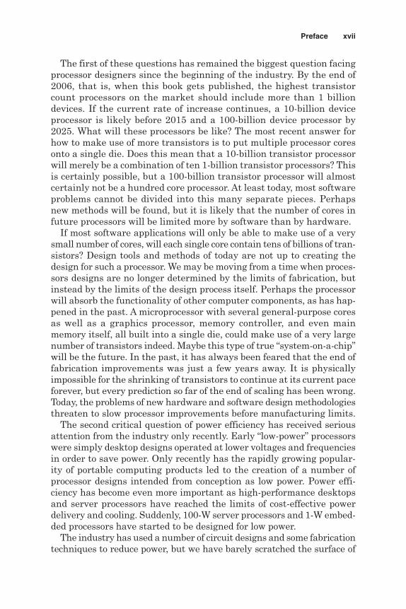
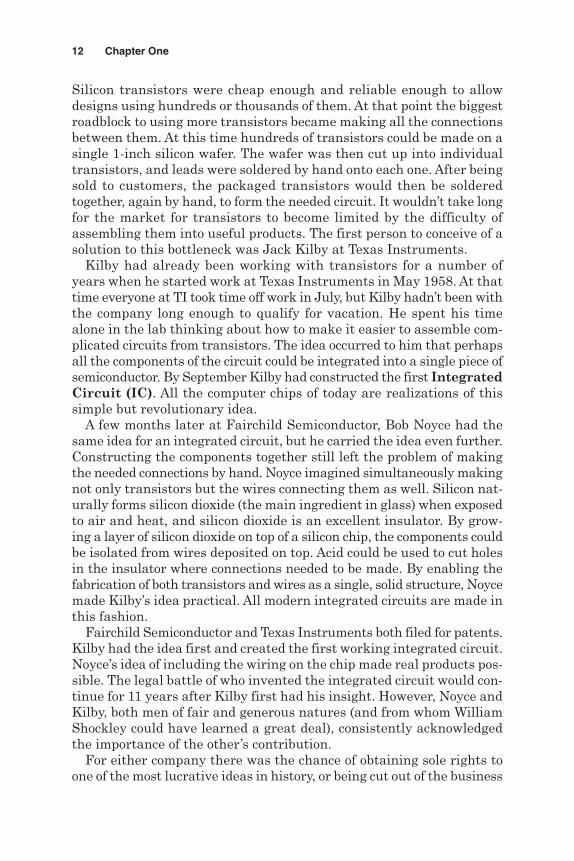
Today we have a much better understanding of why some impurities pro-duce N-type and others P-type semiconductors, and the operation of ajunction diode. Everything is made of atoms and since all atoms containelectrons, anything can conduct electricity. Anyone who has seen a light-ning storm has seen proof that with a sufficiently large electric field, evenair can conduct large amounts of electricity. Materials are classified by howeasily they carry electricity. Materials like copper that conduct easily arecalled conductors, and materials like glass that do not conduct easily arecalled insulators. Some materials, such as silicon, normally do not conducteasily, but very small amounts of impurities cause them to become goodconductors. These materials are called semiconductors. The reason forthis behavior is electron energy bands and band gaps (Fig. 1-1).
Quantum mechanics tells us that electrons can occupy only a finitenumber of discrete energy levels. In any noncrystalline material the
4 Chapter One
6x9 Technical / Microprocessor Design / McFarland /45951-0 / Chapter 1
Energy
Allowed energystates
Conductor InsulatorPure
semiconductor
Bandgap
Band gap
N-typesemiconductor
P-typesemiconductor
Figure 1-1 Energy bands.
951-0 Microproc_CH01.qxd 9/3/06 6:32 PM Page 4
spacing of atoms is nonuniform so the available quantum states varythrough the material, but in a crystal the spacing of atoms is uniformso that continuous bands of allowed energy states are created. In a con-ductor the electrons do not completely fill these bands so that any energyat all will allow them to move through the crystal.
In an insulator the lowest energy band, the valence band, is com-pletely filled with electrons and there is a large energy gap to the nextband, the conduction band, which is completely empty. No currentflows, because there are no open spaces for electrons in the valenceband to move to, and they do not have enough energy to reach the con-duction band. The conduction band has open spaces but has no electronsto carry current.
Semiconductors have a very small band gap between the valence andconduction band. This means that at room temperature a small numberof electrons from the valence band will have enough energy to reach theconduction band. These electrons in the conduction band and the holesthey leave behind in the valence band are now free to move under theinfluence of an electric field and carry current.
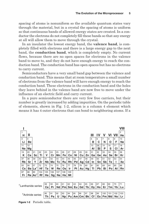
In a pure semiconductor there are very few free carriers, but theirnumber is greatly increased by adding impurities. On the periodic tableof elements, shown in Fig. 1-2, silicon is a column 4 element whichmeans it has 4 outer electrons that can bond to neighboring atoms. If a
The Evolution of the Microprocessor 5
6x9 Technical / Microprocessor Design / McFarland /45951-0 / Chapter 1
1
H3
Li11
Na19
K37
Rb55
Cs87
Fr
4
Be12
Mg20
Ca38
Sr56
Ba88
Ra
21
Sc39
Y57
La∗89
Ac†
22
Ti40
Zr72
Hf104
Rf
23
V41
Nb73
Ta105
Ha
24
Cr42
Mo74
W106
Sg
25
Mn43
Tc75
Re107
Ns
26
Fe44
Ru76
Os108
Hs
27
Co45
Rh77
Ir109
Mt
28
Ni46
Pd78
Pt
29
Cu47
Ag79
Au
30
Zn48
Cd80
Hg
5
B13
Al31
Ga49
In81
Tl
6
C14
Si32
Ge50
Sn82
Pb
7
N15
P33
As51
Sb83
Bi
8
O16
S34
Se52
Te84
Po
9
F17
Cl35
Br53
I85
At
2
He10
Ne18
Ar36
Kr54
Xe86
Rn
58
Ce59
Pr60
Nd61
Pm62
Sm63
Eu64
Gd65
Tb66
Dy67
Ho68
Er69
Tm70
Yb71
Lu
90
Th91
Pa92
U93
Np94
Pu95
Am96
Cm97
Bk98
Cf99
Es100
Fm101
Md102
No103
Lr
∗Lanthanide series
†Actinide series
I
II III IV V VI VII
VIII
Figure 1-2 Periodic table.
951-0 Microproc_CH01.qxd 9/3/06 6:32 PM Page 5
column 5 element such as arsenic or phosphorous is added to a siliconcrystal, these atoms will bond with the 4 neighboring silicon atoms leav-ing one electron left over. This electron is free to move in the conduc-tion band and acts as a negative carrier. Therefore, adding column 5elements creates N-type silicon. Column 3 elements, such as boron,have 3 outer electrons so they naturally create holes in the valenceband, which act as positive charge carriers. Therefore, adding column3 elements creates P-type silicon. Understanding N-type and P-typesilicon allows us to understand Ohl’s P-N junction diode.
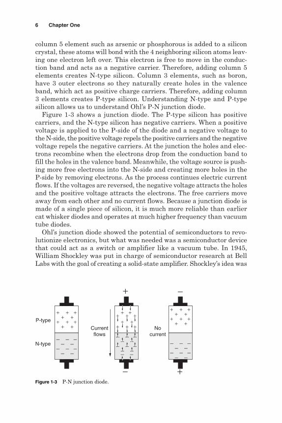
Figure 1-3 shows a junction diode. The P-type silicon has positivecarriers, and the N-type silicon has negative carriers. When a positivevoltage is applied to the P-side of the diode and a negative voltage tothe N-side, the positive voltage repels the positive carriers and the negativevoltage repels the negative carriers. At the junction the holes and elec-trons recombine when the electrons drop from the conduction band tofill the holes in the valence band. Meanwhile, the voltage source is push-ing more free electrons into the N-side and creating more holes in theP-side by removing electrons. As the process continues electric currentflows. If the voltages are reversed, the negative voltage attracts the holesand the positive voltage attracts the electrons. The free carriers moveaway from each other and no current flows. Because a junction diode ismade of a single piece of silicon, it is much more reliable than earliercat whisker diodes and operates at much higher frequency than vacuumtube diodes.
Ohl’s junction diode showed the potential of semiconductors to revo-lutionize electronics, but what was needed was a semiconductor devicethat could act as a switch or amplifier like a vacuum tube. In 1945,William Shockley was put in charge of semiconductor research at BellLabs with the goal of creating a solid-state amplifier. Shockley’s idea was
6 Chapter One
6x9 Technical / Microprocessor Design / McFarland /45951-0 / Chapter 1
++
++
++
++
+
+
−−
−−
−−
−−
−−
++
++
+ ++
+
−−
−−
−−
−−
−−
++
++
++
++
+
+
−−
−−
−−
−−
−−− −
+ +P-type
N-type
Currentflows
Nocurrent
−
−
+
+Figure 1-3 P-N junction diode.
951-0 Microproc_CH01.qxd 9/3/06 6:32 PM Page 6
to use a metal plate placed near the surface of a semiconductor, but nottouching, to control the flow current within the semiconductor. Hebelieved the electric field from the plate could create a channel of chargecarriers within the semiconductor, allowing it to conduct dramaticallymore current than possible when the field was not present. The ideaseemed sound, but when Shockley built an apparatus to test his theory,it didn’t work. Even with 1000 V on the metal plate, he could not measureany amplification at all.
Shockley gave this puzzle to two of the researchers on his team. JohnBardeen was one of very few men in the world at the time with a thor-ough grasp of the physics of semiconductors, and Walter Brattain wasan experienced experimentalist with a reputation as a man who couldbuild anything. Together these two began experiments to determinewhy Shockley’s “field-effect” device did not work. They came to believethat the problem was charges trapped at the surface of the semicon-ductor. If the semiconductor naturally formed a slight excess of electronsat its surface and these charges were unable to move under the influ-ence of an electric field, they would prevent an electric field from pen-etrating the surface and creating amplification. Bardeen and Brattainbegan looking for a way to neutralize these surface charges. They triedplacing the semiconductor in various liquids and got some improve-ment but never with enough amplification at a high enough frequencyto be useful.
Bardeen and Brattain had a piece of germanium (another column 4semiconductor) prepared with a thin oxide layer on top. They hoped theoxide would somehow neutralize the surface charges. Brattain care-fully cleaned the crystal and began testing. At first his results made nosense at all. The device responded as if the oxide layer wasn’t eventhere. Then to his horror, Brattain realized that in cleaning the crystalhe had accidentally removed the oxide layer. Germanium oxide is solu-ble in water. Without the oxide layer what he had created was a numberof cat whisker diodes on the same piece of semiconductor. Frustrated,he continued experimenting with the device anyway and was surprisedto find some amplification between the diodes. Perhaps neutralizingthe surface charges wasn’t necessary at all.
They decided to try two cat whisker diodes touching the same semi-conductor crystal at almost the same point. In December 1947, theywrapped a piece of gold foil around a triangular piece of plastic andthen used a razor blade to make a cut in the gold at the point of the tri-angle. By touching the point of the triangle to a piece of germanium crys-tal, they created two cat whisker diodes. They discovered that electronsemitted into the semiconductor by one diode were collected by the other.The voltage on the crystal base could increase or suppress this effectallowing their device to amplify the signal at the base. Because a control
The Evolution of the Microprocessor 7
6x9 Technical / Microprocessor Design / McFarland /45951-0 / Chapter 1
951-0 Microproc_CH01.qxd 9/3/06 6:32 PM Page 7

could vary the resistance between emitter and collector, it was laterdecided to call the device a transfer-resistor or transistor.
It was immediately apparent that the transistor would be anextremely important innovation and Bell Labs began the process ofapplying for a patent immediately. Shockley felt that Bardeen andBrattain’s success had come as a result of his field-effect concept and thatBell Labs should file a broad patent to include his field-effect ideas andthe newly created transistor. Furthermore, as leader of the team,Shockley felt that his name alone should appear on the patent.Shockley’s harmonious research team quickly became polarized overthe question of who should receive credit for the new invention. Bell Labattorneys might have given Shockley what he wanted, but in reviewingthe patents already on record they found something disturbing.
An obscure physics professor named Julius Lilienfeld had beengranted two patents in 1930 and 1933 for the idea of controlling the cur-rent in a semiconductor by means of an electric field. Although there wasno record of Lilienfeld ever trying to build his device and surface chargeswould almost certainly have prevented it from working if he did, the ideawas clearly the same as Shockley’s. A patent on a field-effect transistorwould almost certainly be overturned. The attorneys at Bell Labsdecided to write a more narrow patent application focusing just onBardeen and Brattian’s point-contact transistor, which worked on dif-ferent principles. Ultimately patent 2524035, “Three-Electrode CircuitElement Utilizing Semiconductive Materials” lists only Bardeen andBrattain as inventors.
Shockley felt he had been robbed of proper credit and began workingon his own to devise a new and better transistor. The point-contact tran-sistor shared all the same problems as cat whisker diodes. Because itrequired two metal lines to just touch the surface of the semiconductorit was extremely temperamental and hard to consistently reproduce.Shockley reasoned that if a transistor could be formed out of two catwhisker diodes sharing one terminal, perhaps he could make a transistorout of two junction diodes sharing one terminal.
He began working out the theory of a junction transistor but told no oneat Bell Labs until February 1948, when experiments with the point-contacttransistor suggested that charge carriers could travel through the bulkof semiconductors and not just at the surface as Bardeen and Brattainhad been assuming. Knowing this was proof that his concept for atransistor could work, Shockley now described his ideas to the group.It was obvious to Bardeen and Brattain that Shockley had been thinkingabout this for some time and intentionally kept them in the dark. In June1948, despite not yet having a working prototype, Bell Labs applied fora patent of the junction transistor listing only Shockley’s name. Bardeenand Brattain would never work effectively with Shockley again.
8 Chapter One
6x9 Technical / Microprocessor Design / McFarland /45951-0 / Chapter 1
951-0 Microproc_CH01.qxd 9/3/06 6:32 PM Page 8

Under Shockley’s direction, Morgan Sparks built the first workingjunction transistor in 1949; by 1950, Sparks and Gordon Teal had vastlyimproved their techniques. For the previous 2 years, Teal had been advo-cating making semiconductor devices out of single crystals. The “crystals”used at the time were really just amalgams of many crystals all with dif-ferent orientations and many noncrystalline defects in between. Tealbuilt an apparatus to grow single crystals semiconductors without thesedefects using the ideas of the Polish scientist J. Czochralski.
Using Czochralski’s method, a very small seed crystal is dipped into acontainer of molten semiconductor and very slowly pulled out. As thecrystal is pulled out, atoms from the melt freeze onto its surface, grad-ually growing the crystal. Each atom tends to freeze into proper place inthe crystal lattice producing a large defect-free crystal. Also importantis that impurities in the melt tend to stay in the melt. The crystal drawnout is purer than the starting material. By repeatedly drawing crystalsand then melting them down to be drawn again, Teal achieved puritylevels vastly better than anything Shockley had worked with thus far.In later years, the cylindrical ingots pulled from the melt would be slicedinto the round silicon wafers used today. Using these new techniques,Sparks and Teal created the junction transistor Shockley had imagined.
Rather than two diodes side by side, Shockley imagined a sandwichof three semiconductor layers alternating N-type, P-type, and N-type asshown in Fig. 1-4. The emitter at the bottom injects electrons into thebase in the center. These electrons diffuse across the base to be capturedby the collector at the top. The voltage on the base controls the injec-tion of electrons by the emitter. Because this device contains two P-N
The Evolution of the Microprocessor 9
6x9 Technical / Microprocessor Design / McFarland /45951-0 / Chapter 1
Currentflows
P-typebase
N-typeemitter
N-typecollector
Nocurrent
+ +
+ +
−−
−−
−−
−−
−− −
−−
−−
−−
−
−−− −
−−
−−
−−
−−
−−
−−
−−
−−
−−
−−
+ +
+ +
−−
−−
−−
−−
−−
−−
−−
−−
−−
−−
−− − −
+ +
+ +
− − −
−
+
+
+
−Figure 1-4 Junction transistor.
951-0 Microproc_CH01.qxd 9/3/06 6:32 PM Page 9
junctions, this device is known as the Bipolar Junction Transistor(BJT). Sparks and Teal were able to create this structure by addingdopants to the melt as they pulled the crystal. Pulling the crystal moreslowly created thinner layers and improved performance.
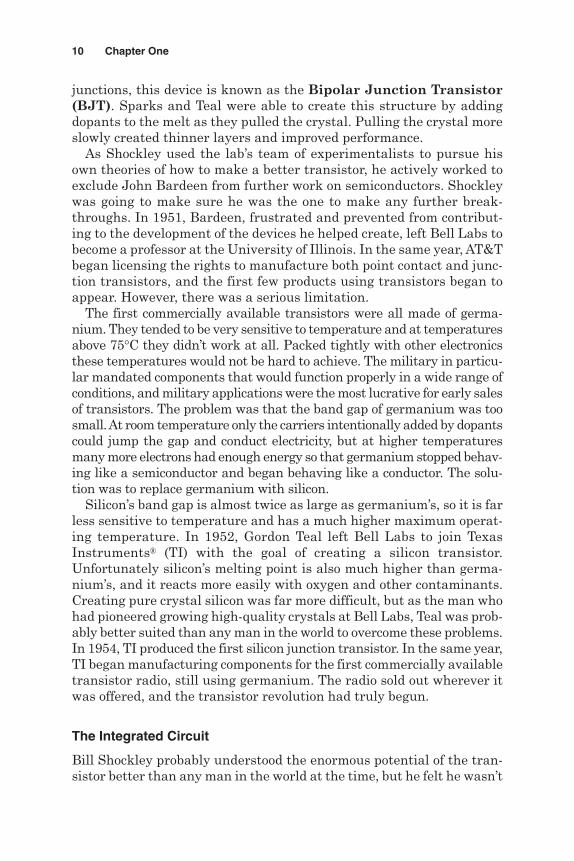
As Shockley used the lab’s team of experimentalists to pursue hisown theories of how to make a better transistor, he actively worked toexclude John Bardeen from further work on semiconductors. Shockleywas going to make sure he was the one to make any further break-throughs. In 1951, Bardeen, frustrated and prevented from contribut-ing to the development of the devices he helped create, left Bell Labs tobecome a professor at the University of Illinois. In the same year, AT&Tbegan licensing the rights to manufacture both point contact and junc-tion transistors, and the first few products using transistors began toappear. However, there was a serious limitation.
The first commercially available transistors were all made of germa-nium. They tended to be very sensitive to temperature and at temperaturesabove 75°C they didn’t work at all. Packed tightly with other electronicsthese temperatures would not be hard to achieve. The military in particu-lar mandated components that would function properly in a wide range ofconditions, and military applications were the most lucrative for early salesof transistors. The problem was that the band gap of germanium was toosmall. At room temperature only the carriers intentionally added by dopantscould jump the gap and conduct electricity, but at higher temperaturesmany more electrons had enough energy so that germanium stopped behav-ing like a semiconductor and began behaving like a conductor. The solu-tion was to replace germanium with silicon.
Silicon’s band gap is almost twice as large as germanium’s, so it is farless sensitive to temperature and has a much higher maximum operat-ing temperature. In 1952, Gordon Teal left Bell Labs to join TexasInstruments® (TI) with the goal of creating a silicon transistor.Unfortunately silicon’s melting point is also much higher than germa-nium’s, and it reacts more easily with oxygen and other contaminants.Creating pure crystal silicon was far more difficult, but as the man whohad pioneered growing high-quality crystals at Bell Labs, Teal was prob-ably better suited than any man in the world to overcome these problems.In 1954, TI produced the first silicon junction transistor. In the same year,TI began manufacturing components for the first commercially availabletransistor radio, still using germanium. The radio sold out wherever itwas offered, and the transistor revolution had truly begun.
The Integrated Circuit
Bill Shockley probably understood the enormous potential of the tran-sistor better than any man in the world at the time, but he felt he wasn’t
10 Chapter One
6x9 Technical / Microprocessor Design / McFarland /45951-0 / Chapter 1
951-0 Microproc_CH01.qxd 9/3/06 6:32 PM Page 10

being given sufficient authority at Bell Labs. More than once he hadwatched other men promoted over him. Also, Shockley personally wouldnot receive any money from the transistor patents he had helped AT&Tsecure. He decided to leave and found his own company to make semi-conductor products.
In the fall of 1955, Shockley secured financially backing fromCalifornia businessman Arnold Beckman and chose Palo Alto, California,as the location for his new company. At the time Palo Alto was notableonly as the home of Stanford University. Shockley had received strongencouragement from Frederick Terman, the Stanford Dean ofEngineering, to locate nearby. The university’s engineering school wouldbe an ideal place to recruit new employees, but perhaps Shockley wasultimately persuaded by more personal reasons. He had grown up inPalo Alto, and his mother still lived there. Over the next 20 years,Shockley’s decision would cause this sleepy valley of orchards to betransformed into the famous “Silicon Valley.”
Perhaps not surprisingly, Shockley had little luck hiring any of hisformer colleagues from Bell Labs, and so he turned to a younger gen-eration. He recruited some of the brightest engineers, physicists, andchemists from around the country, and in February 1956, ShockleySemiconductor was founded. That same year, Shockley, Bardeen, andBrattain were together awarded the Nobel Prize in physics for theirinvention of the transistor. Shockley’s brilliance as a scientist hadreceived the highest recognition, and yet it was his management stylethat would doom his company.
Feeling that his subordinates at Bell Labs had tried to steal the creditfor his ideas, Shockley was determined that it would not happen at hisown company. All ideas and all development direction were to comefrom him. The talented men he hired grew restless under his heavy-handed management. In 1957, eight of Shockley’s recruits, led by RobertNoyce and Gordon Moore, approached Beckman to ask that Shockley beremoved from management and allowed to act only as a technical con-sultant. Beckman considered this seriously for a month before decidingto leave Shockley in charge. On September 18, 1957, the group thatwould become known in Silicon Valley as the “traitorous eight” resigned.Shockley Semiconductor continued operating another 11 years but neverturned a profit. Bill Shockley never again had a significant influence onthe semiconductor industry he had helped to start.
The day after the “eight” resigned they founded a new company,Fairchild Semiconductor, in which Fairchild Camera and Instrumentsprovided the financial backing. The company was becoming involved incomponents for missiles and satellites, and it was clear that transistorswould play an important part. Fairchild Semiconductor made rapidprogress and by 1959 was profitably selling silicon junction transistors.
The Evolution of the Microprocessor 11
6x9 Technical / Microprocessor Design / McFarland /45951-0 / Chapter 1
951-0 Microproc_CH01.qxd 9/3/06 6:32 PM Page 11
Silicon transistors were cheap enough and reliable enough to allowdesigns using hundreds or thousands of them. At that point the biggestroadblock to using more transistors became making all the connectionsbetween them. At this time hundreds of transistors could be made on asingle 1-inch silicon wafer. The wafer was then cut up into individualtransistors, and leads were soldered by hand onto each one. After beingsold to customers, the packaged transistors would then be solderedtogether, again by hand, to form the needed circuit. It wouldn’t take longfor the market for transistors to become limited by the difficulty ofassembling them into useful products. The first person to conceive of asolution to this bottleneck was Jack Kilby at Texas Instruments.
Kilby had already been working with transistors for a number ofyears when he started work at Texas Instruments in May 1958. At thattime everyone at TI took time off work in July, but Kilby hadn’t been withthe company long enough to qualify for vacation. He spent his timealone in the lab thinking about how to make it easier to assemble com-plicated circuits from transistors. The idea occurred to him that perhapsall the components of the circuit could be integrated into a single piece ofsemiconductor. By September Kilby had constructed the first IntegratedCircuit (IC). All the computer chips of today are realizations of thissimple but revolutionary idea.
A few months later at Fairchild Semiconductor, Bob Noyce had thesame idea for an integrated circuit, but he carried the idea even further.Constructing the components together still left the problem of makingthe needed connections by hand. Noyce imagined simultaneously makingnot only transistors but the wires connecting them as well. Silicon nat-urally forms silicon dioxide (the main ingredient in glass) when exposedto air and heat, and silicon dioxide is an excellent insulator. By grow-ing a layer of silicon dioxide on top of a silicon chip, the components couldbe isolated from wires deposited on top. Acid could be used to cut holesin the insulator where connections needed to be made. By enabling thefabrication of both transistors and wires as a single, solid structure, Noycemade Kilby’s idea practical. All modern integrated circuits are made inthis fashion.
Fairchild Semiconductor and Texas Instruments both filed for patents.Kilby had the idea first and created the first working integrated circuit.Noyce’s idea of including the wiring on the chip made real products pos-sible. The legal battle of who invented the integrated circuit would con-tinue for 11 years after Kilby first had his insight. However, Noyce andKilby, both men of fair and generous natures (and from whom WilliamShockley could have learned a great deal), consistently acknowledgedthe importance of the other’s contribution.
For either company there was the chance of obtaining sole rights toone of the most lucrative ideas in history, or being cut out of the business
12 Chapter One
6x9 Technical / Microprocessor Design / McFarland /45951-0 / Chapter 1
951-0 Microproc_CH01.qxd 9/3/06 6:32 PM Page 12

altogether. The courts could easily decide for either side. Rather thanpursue total victory at the risk of total destruction, in 1966, both compa-nies agreed to cross license their patents to each other. They also agreedto sell licenses for both patents for a small percentage of the profits, toanyone else who wanted to make integrated circuits. When later courtcases found first in favor of Kilby and then in favor of Noyce, it no longermattered, and today they are considered coinventors of the integratedcircuit.
In 1960, Bell Labs made another key advance, creating the first suc-cessful field-effect transistor. This was the same transistor that Shockleyhad originally set out to build 15 years earlier and Lilienfeld had firstproposed 15 years before that, but no one had been able to make itwork. The key turned out to be the same silicon dioxide layer that Noycehad proposed using. A group headed by John Atalla showed that bycarefully cleaning the silicon surface and then growing an oxide layerthe surface states could be eliminated. The electric field from a metalwire deposited on top of the oxide could penetrate the silicon and turnon and off a flow of current. Because it was a vertical stack of metal,oxide, and semiconductor, this device was named the Metal OxideSemiconductor Field-Effect Transistor (MOSFET).
Figure 1-5 shows a MOSFET that is off and one that is on. Each con-sists of metal input and output wires that touch the silicon. Where theytouch the silicon, impurities have been added to allow the silicon to con-duct. These regions of dopants added to the silicon are the transistor’ssource and drain. The source will provide the electrical charges that willbe removed by the drain. In between the source and drain, a third con-ducting wire passes very close to but does not touch the silicon. This wireis the gate of the transistor, and we can imagine it swinging open or
The Evolution of the Microprocessor 13
6x9 Technical / Microprocessor Design / McFarland /45951-0 / Chapter 1
P-type
N-typesource
N-typedrain
Gate
P-type
OxideOxideN-typesource
N-typedrain
Gate
Gate voltage lowTransistor OFFNo current flow
Gate voltage highTransistor ONCurrent flows
+− − − + +
Figure 1-5 MOSFET transistor cross sections.
951-0 Microproc_CH01.qxd 9/3/06 6:32 PM Page 13
closed to turn the transistor on or off. The voltage of the gate wire pro-duces an electric field which determines whether current can flow fromthe source to the drain or not. In the left figure, a low voltage at the gaterepels the negative charges in the source and drain and keeps them sep-arated. In the right figure, a high voltage at the gate attracts the neg-ative charges and pulls them together into a channel connecting thesource and drain. Where bipolar junction transistors require a constantcurrent into the base to remain switched on, MOSFETs require only avoltage to be held at the gate. This allows MOSFETs to use less powerthan equivalent BJT circuits. Almost all transistors made today areMOSFETs connected together in integrated circuits.
The Microprocessor
The integrated circuit was not an immediate commercial success. By1960 the computer had gone from a laboratory device to big businesswith thousands in operation worldwide and more than half a billion dol-lars in sales in 1960 alone.2 International Business Machines (IBM®) hadbecome the leading computer manufacturer and had just begun shippingits first all-transistorized computer. These machines still bore little resem-blance to the computers of today. Costing millions these “mainframe”computers filled rooms and required teams of operators to man them.Integrated circuits would reduce the cost of assembling these computersbut not nearly enough to offset their high prices compared to discrete tran-sistors. Without a large market the volume production that would bringintegrated circuit costs down couldn’t happen. Then, in 1961, PresidentKennedy challenged the United States to put a man on the moon beforethe end of the decade. To do this would require extremely compact andlight computers, and cost was not a limitation. For the next 3 years, thenewly created space agency, NASA, and the U.S. Defense Departmentpurchased every integrated circuit made and demand soared.
The key to making integrated circuits cost effective enough for the gen-eral market place was incorporating more transistors into each chip.The size of early MOSFETs was limited by the problem of making thegate cross exactly between the source and drain. Adding dopants to formthe source and drain regions requires very high temperatures that wouldmelt a metal gate wire. This forced the metal gates to be formed afterthe source and drain, and ensuring the gates were properly aligned wasa difficult problem. In 1967, Fedrico Faggin at Fairchild Semiconductorexperimented with making the gate wires out of silicon. Because the sil-icon was deposited on top of an oxide layer, it was not a single crystal
14 Chapter One
6x9 Technical / Microprocessor Design / McFarland /45951-0 / Chapter 1
2Einstein and Franklin, “Computer Manufacturing,” 10.
951-0 Microproc_CH01.qxd 9/3/06 6:32 PM Page 14
but a jumble of many small crystals called polycrystalline silicon,polysilicon, or just poly. By forming polysilicon gates before adding dopants,the gate itself would determine where the dopants would enter thesilicon crystal. The result was a self-aligned MOSFET. The resistanceof polysilicon is much higher than a metal conductor, but with heavydoping it is low enough to be useful. MOSFETs are still made with polygates today.
The computers of the 1960s stored their data and instructions in“core” memory. These memories were constructed of grids of wires withmetal donuts threaded onto each intersection point. By applying currentto one vertical and one horizontal wire a specific donut or “core” couldbe magnetized in one direction or the other to store a single bit of infor-mation. Core memory was reliable but difficult to assemble and oper-ated slowly compared to the transistors performing computations. Amemory made out of transistors was possible but would require thou-sands of transistors to provide enough storage to be useful. Assemblingthis by hand wasn’t practical, but the transistors and connections neededwould be a simple pattern repeated many times, making semiconductormemory a perfect market for the early integrated circuit business.
In 1968, Bob Noyce and Gordon Moore left Fairchild Semiconductorto start their own company focused on building products from inte-grated circuits. They named their company Intel® (from INTegratedELectronics). In 1969, Intel began shipping the first commercial inte-grated circuit using MOSFETs, a 256-bit memory chip called the 1101.The 1101 memory chip did not sell well, but Intel was able to rapidlyshrink the size of the new silicon gate MOSFETs and add more tran-sistors to their designs. One year later Intel offered the 1103 with 1024bits of memory, and this rapidly became a standard component in thecomputers of the day.
Although focused on memory chips, Intel received a contract to designa set of chips for a desktop calculator to be built by the Japanese com-pany Busicom. At that time, calculators were either mechanical or usedhard-wired logic circuits to do the required calculations. Ted Hoff wasasked to design the chips for the calculator and came to the conclusionthat creating a general purpose processing chip that would read instruc-tions from a memory chip could reduce the number of logic chipsrequired. Stan Mazor detailed how the chips would work together andafter much convincing Busicom agreed to accept Intel’s design. Therewould be four chips altogether: one chip controlling input and outputfunctions, a memory chip to hold data, another to hold instructions,and a central processing unit that would eventually become the world’sfirst microprocessor.
The computer processors that powered the mainframe computers of theday were assembled from thousands of discrete transistors and logic chips.
The Evolution of the Microprocessor 15
6x9 Technical / Microprocessor Design / McFarland /45951-0 / Chapter 1
951-0 Microproc_CH01.qxd 9/3/06 6:32 PM Page 15
This was the first serious proposal to put all the logic of a computerprocessor onto a single chip. However, Hoff had no experience withMOSFETs and did not know how to make his design a reality. Thememory chips Intel was making at the time were logically very simplewith the same basic memory cell circuit repeated over and over. Hoff ’sdesign would require much more complicated logic and circuit designthan any integrated circuit yet attempted. For months no progress wasmade as Intel struggled to find someone who could implement Hoff ’s idea.
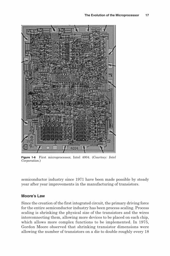
In April 1970, Intel hired Faggin, the inventor of the silicon gateMOSFET, away from Fairchild. On Faggin’s second day at Intel, MasatoshiShima, the engineering representative from Busicom, arrived from Japanto review the design. Faggin had nothing to show him but the same plansShima had already reviewed half a year earlier. Shima was furious, andFaggin finished his second day at a new job already 6 months behindschedule. Faggin began working at a furious pace with Shima helpingto validate the design, and amazingly by February 1971 they had all fourchips working. The chips processed data 4 bits at a time and so werenamed the 4000 series. The fourth chip of the series was the first micro-processor, the Intel 4004 (Fig. 1-6).
The 4004 contained 2300 transistors and ran at a clock speed of 740 kHz,executing on average about 60,000 instructions per second.3 This gave itthe same processing power as early computers that had filled entirerooms, but on a chip that was only 24 mm2. It was an incredible engi-neering achievement, but at the time it was not at all clear that it had acommercial future. The 4004 might match the performance of the fastestcomputer in the world in the late 1940s, but the mainframe computersof 1971 were hundreds of times faster. Intel began shipping the 4000series to Busicom in March 1971, but the calculator market had becomeintensely competitive and Busicom was unenthusiastic about the high costof the 4000 series. To make matters worse, Intel’s contract with Busicomspecified Intel could not sell the chips to anyone else. Hoff, Faggin, andMazor pleaded with Intel’s management to secure the right to sell toother customers. Bob Noyce offered Busicom a reduced price for the 4000series if they would change the contract, and desperate to cut costs in orderto stay in business Busicom agreed. By the end of 1971, Intel was mar-keting the 4004 as a general purpose microprocessor. Busicom ultimatelysold about 100,000 of the series 4000 calculators before going out of busi-ness in 1974. Intel would go on to become the leading manufacturer inwhat was for 2003—a $27 billion a year market for microprocessors. Theincredible improvements in microprocessor performance and growth of the
16 Chapter One
6x9 Technical / Microprocessor Design / McFarland /45951-0 / Chapter 1
3Real, “Revolution in Progress,” 12.
951-0 Microproc_CH01.qxd 9/3/06 6:32 PM Page 16
semiconductor industry since 1971 have been made possible by steadyyear after year improvements in the manufacturing of transistors.
Moore’s Law
Since the creation of the first integrated circuit, the primary driving forcefor the entire semiconductor industry has been process scaling. Processscaling is shrinking the physical size of the transistors and the wiresinterconnecting them, allowing more devices to be placed on each chip,which allows more complex functions to be implemented. In 1975,Gordon Moore observed that shrinking transistor dimensions wereallowing the number of transistors on a die to double roughly every 18
The Evolution of the Microprocessor 17
6x9 Technical / Microprocessor Design / McFarland /45951-0 / Chapter 1
Figure 1-6 First microprocessor, Intel 4004. (Courtesy: IntelCorporation.)
951-0 Microproc_CH01.qxd 9/3/06 6:32 PM Page 17
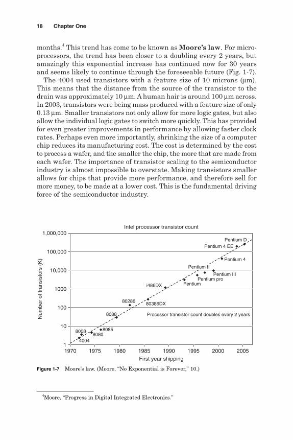
months.4 This trend has come to be known as Moore’s law. For micro-processors, the trend has been closer to a doubling every 2 years, butamazingly this exponential increase has continued now for 30 yearsand seems likely to continue through the foreseeable future (Fig. 1-7).
The 4004 used transistors with a feature size of 10 microns (µm).This means that the distance from the source of the transistor to thedrain was approximately 10 µm. A human hair is around 100 µm across.In 2003, transistors were being mass produced with a feature size of only0.13 µm. Smaller transistors not only allow for more logic gates, but alsoallow the individual logic gates to switch more quickly. This has providedfor even greater improvements in performance by allowing faster clockrates. Perhaps even more importantly, shrinking the size of a computerchip reduces its manufacturing cost. The cost is determined by the costto process a wafer, and the smaller the chip, the more that are made fromeach wafer. The importance of transistor scaling to the semiconductorindustry is almost impossible to overstate. Making transistors smallerallows for chips that provide more performance, and therefore sell formore money, to be made at a lower cost. This is the fundamental drivingforce of the semiconductor industry.
18 Chapter One
6x9 Technical / Microprocessor Design / McFarland /45951-0 / Chapter 1
1,000,000
100,000
10,000
1000
100
Num
ber
of tr
ansi
stor
s (K
)
10
11970 1975 1980
40048080
80858008
8088
80286 80386DX
i486DX PentiumPentium pro
Pentium III
Pentium 4
Pentium 4 EEPentium D
1985 1990
First year shipping
Processor transistor count doubles every 2 years
Intel processor transistor count
1995 2000 2005
Pentium II
Figure 1-7 Moore’s law. (Moore, “No Exponential is Forever,” 10.)
4Moore, “Progress in Digital Integrated Electronics.”
951-0 Microproc_CH01.qxd 9/3/06 6:32 PM Page 18
Transistor scaling
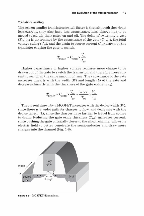
The reason smaller transistors switch faster is that although they drawless current, they also have less capacitance. Less charge has to bemoved to switch their gates on and off. The delay of switching a gate(TDELAY) is determined by the capacitance of the gate (CGATE), the totalvoltage swing (Vdd), and the drain to source current (IDS) drawn by thetransistor causing the gate to switch.
Higher capacitance or higher voltage requires more charge to bedrawn out of the gate to switch the transistor, and therefore more cur-rent to switch in the same amount of time. The capacitance of the gateincreases linearly with the width (W) and length (L) of the gate anddecreases linearly with the thickness of the gate oxide (TOX).
The current drawn by a MOSFET increases with the device width (W ),since there is a wider path for charges to flow, and decreases with thedevice length (L), since the charges have farther to travel from sourceto drain. Reducing the gate oxide thickness (TOX) increases current,since pushing the gate physically closer to the silicon channel allows itselectric field to better penetrate the semiconductor and draw morecharges into the channel (Fig. 1-8).
T CV
IW L
T
V
IDELAY GATEdd
DS OX
dd
DS
∝ × ∝ × ×
T CV
IDELAY GATEdd
DS
∝ ×
The Evolution of the Microprocessor 19
6x9 Technical / Microprocessor Design / McFarland /45951-0 / Chapter 1
Length
TOX
Source Drain
Width
Polygate
Figure 1-8 MOSFET dimensions.
951-0 Microproc_CH01.qxd 9/3/06 6:32 PM Page 19

To draw any current at all, the gate voltage must be greater than acertain minimum voltage called the threshold voltage (VT). This volt-age is determined by both the gate oxide thickness and the concentra-tion of dopant atoms added to the channel. Current from the drain tosource increases quadratically after the threshold voltage is crossed. Thecurrent of MOSFETs is discussed in more detail in Chap. 7.
Putting together these equations for delay and current we find:
Decreasing device lengths, increasing voltage, or decreasing thresholdvoltage reduces the delay of a MOSFET. Of these methods decreasing thedevice length is the most effective, and this is what the semiconductorindustry has focused on the most. There are different ways to measurechannel length, and so when comparing one process to another, it isimportant to be clear on which measurement is being compared. Channellength is measured by three different values as shown in Fig. 1-9.
The drawn gate length (LDRAWN) is the width of the gate wire as drawnon the mask used to create the transistors. This is how wide the wire willbe when it begins processing. The etching process reduces the width of theactual wire to less than what was drawn on the mask. The manufacturingof MOSFETs is discussed in detail in Chap. 9. The width of the gate wire
T LV
V VDELAY∝ ×
−2 dd
dd T2( )
IW
L TV V
TDS
OX
dd2( )∝
×× −
20 Chapter One
6x9 Technical / Microprocessor Design / McFarland /45951-0 / Chapter 1
Figure 1-9 Channel length.
LEFF
Gate
DrainSource
Mask
Poly
SiO2
Si
LDRAWN
LGATE
951-0 Microproc_CH01.qxd 9/3/06 6:32 PM Page 20
at the end of processing is the actual gate length (LGATE). Also, the sourceand drain regions within the silicon typically reach some distance under-neath the gate. This makes the effective separation between source anddrain in the silicon less than the final gate length. This distance is calledthe effective channel length (LEFF). It is this effective distance that is themost important to transistor performance, but because it is under thegate and inside the silicon, it can not be measured directly. LEFF is onlyestimated by electrical measurements. Therefore, LGATE is the value mostcommonly used to compare difference processes.
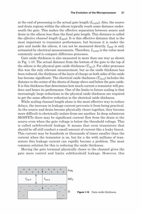
Gate oxide thickness is also measured in more than one way as shownin Fig. 1-10. The actual distance from the bottom of the gate to the top ofthe silicon is the physical gate oxide thickness (TOX-P). For older processesthis was the only relevant measurement, but as the oxide thickness hasbeen reduced, the thickness of the layer of charge on both sides of the oxidehas become significant. The electrical oxide thickness (TOX-E) includes thedistance to the center of the sheets of charge above and below the gate oxide.It is this thickness that determines how much current a transistor will pro-duce and hence its performance. One of the limits to future scaling is thatincreasingly large reductions in the physical oxide thickness are requiredto get the same effective reduction in the electrical oxide thickness.
While scaling channel length alone is the most effective way to reducedelays, the increase in leakage current prevents it from being practical.As the source and drain become physically closer together, they becomemore difficult to electrically isolate from one another. In deep submicronMOSFETs there may be significant current flow from the drain to thesource even when the gate voltage is below the threshold voltage. Thisis called subthreshold leakage. It means that even transistors thatshould be off still conduct a small amount of current like a leaky faucet.This current may be hundreds or thousands of times smaller than thecurrent when the transistor is on, but for a die with millions of tran-sistors this leakage current can rapidly become a problem. The mostcommon solution for this is reducing the oxide thickness.
Moving the gate terminal physically closer to the channel gives thegate more control and limits subthreshold leakage. However, this
The Evolution of the Microprocessor 21
6x9 Technical / Microprocessor Design / McFarland /45951-0 / Chapter 1
−−
−−
− −
Poly
SiO2
Si
++
++
++
+++
++
++
++
−−
−−
−−
−−
−−−
TOX-P TOX-E
Figure 1-10 Gate oxide thickness.
951-0 Microproc_CH01.qxd 9/3/06 6:32 PM Page 21
reduces the long-term reliability of the transistors. Any material will con-duct electricity if a sufficient electrical field is applied. In the case of insu-lators this is called dielectric breakdown and physically melts thematerial. At extremely high electric fields the electrons, which bindthe molecules of the material together, are torn free and suddenly largeamounts of current begin to flow. The gate oxides of working MOSFETsaccumulate defects over time that gradually lower the field at which thetransistor will fail. These defects can also reduce the switching speedof the transistors.5 These phenomena are particularly worrisome tosemiconductor manufacturers because they can cause a new product tobegin failing after it has already been shipping for months or years.
The accumulation of defects in the gate oxide is in part due to “hot”electron effects. Normally the electrons in the channel do not have enoughenergy to enter the gate oxide. Its band gap is far too large for any sig-nificant number of electrons to have enough energy to surmount atnormal operating temperatures. Electrons in the channel drift fromsource to drain due to the lateral electric field in the channel. Their aver-age drift velocity is determined by how strong the electric field is and howoften the electrons collide with the atoms of the semiconductor crystal.Typically the drift velocity is only a tiny fraction of the random thermalvelocity of the electrons, but at very high lateral fields some electrons mayget accelerated to velocities much higher than they would usually haveat the operating temperature. It is as if these electrons are at a muchhigher temperature than the rest, and they may have enough energy toenter the gate oxide. They may travel through and create a current atthe gate, or they may become trapped in the oxide creating a defect. If aseries of defects happens to line up on a path from the gate to the chan-nel, gate oxide breakdown occurs. Thus the reliability of the transistorsis a limit to how much their dimensions can be scaled. In addition, as gateoxides are scaled below 5 nm, gate tunneling current becomes significant.
One implication of quantum mechanics is that the position of an elec-tron is not precisely defined. This means that with a sufficiently thinoxide layer, electrons will occasionally appear on the opposite side of theinsulator. If there is an electric field, the electron will then be pulledaway and unable to get back. The current this phenomenon createsthrough the insulator is called a tunneling current. It does not damage thelayer as occurs with hot electrons because the electron does not travelthrough the oxide in the classical sense, but this does cause unwantedleakage current through the gate of any ON device. The typical solutionfor both dielectric breakdown and gate tunneling current is to reducethe supply voltage.
22 Chapter One
6x9 Technical / Microprocessor Design / McFarland /45951-0 / Chapter 1
5Chen, “Dynamic NBTI of p-MOS Transistors.”
951-0 Microproc_CH01.qxd 9/3/06 6:32 PM Page 22

Scaling the supply voltage by the same amount as the channel lengthand oxide thickness keeps all the electrical fields in the device constant.This concept is called constant field scaling and was proposed by RobertDennard in 1974.6 Constant field scaling is an easy way to address prob-lems such as subthreshold leakage and dielectric breakdown, but ahigher supply voltage provides for better performance. As a result, theindustry has scaled voltages as slowly as possible, allowing fields inthe channel and the oxide to increase significantly with each devicegeneration. This has required many process adjustments to tolerate thehigher fields. The concentration of dopants in the source, drain, andchannel is precisely controlled to create a three-dimensional profile thatminimizes subthreshold leakage and hot electron effects. Still, even thevery gradual scaling of supply voltages increases delay and hurts per-formance. This penalty increases dramatically when the supply voltagebecomes less than about three times the threshold voltage.
It is possible to design integrated circuits that operate with supplyvoltages less than the threshold voltages of the devices. These designsoperate using only subthreshold leakage currents and as a result areincredibly power efficient. However, because the currents being used areorders of magnitude smaller than full ON currents, the delays involvedare orders of magnitude larger. This is a good trade-off for a chip to gointo a digital watch but not acceptable for a desktop computer. To main-tain reasonable performance a processor must use a supply voltage sev-eral times larger than the threshold voltage. To gain performance atlower supply voltages the channel doping can be reduced to lower thethreshold voltage.
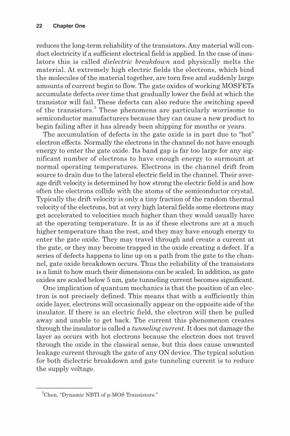
Lowering the threshold voltage immediately provides for more oncurrent but increases subthreshold current much more rapidly. Therate at which subthreshold currents increase with reduced thresholdvoltage is called the subthreshold slope and a typical value is 100mV/decade. This means a 100-mV drop in threshold will increase sub-threshold leakage by a factor of 10. The need to maintain several ordersof magnitude difference between the on and off current of a device there-fore limits how much the threshold voltage can be reduced. Because theincrease in subthreshold current was the first problem encounteredwhen scaling the channel length, we have come full circle to the origi-nal problem. In the end there is no easy solution and process engineersare continuing to look for new materials and structures that will allowthem to reduce delay while controlling leakage currents and reliability(Fig. 1-11).
The Evolution of the Microprocessor 23
6x9 Technical / Microprocessor Design / McFarland /45951-0 / Chapter 1
6Dennard, “MOSFETs with Small Dimensions.”
951-0 Microproc_CH01.qxd 9/3/06 6:32 PM Page 23
Interconnect scaling
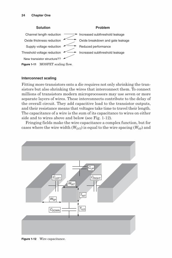
Fitting more transistors onto a die requires not only shrinking the tran-sistors but also shrinking the wires that interconnect them. To connectmillions of transistors modern microprocessors may use seven or moreseparate layers of wires. These interconnects contribute to the delay ofthe overall circuit. They add capacitive load to the transistor outputs,and their resistance means that voltages take time to travel their length.The capacitance of a wire is the sum of its capacitance to wires on eitherside and to wires above and below (see Fig. 1-12).
Fringing fields make the wire capacitance a complex function, but forcases where the wire width (WINT) is equal to the wire spacing (WSP) and
24 Chapter One
6x9 Technical / Microprocessor Design / McFarland /45951-0 / Chapter 1
Increased subthreshold leakage
Oxide breakdown and gate leakage
Reduced performance
Increased subthreshold leakage
Channel length reduction
Oxide thickness reduction
Supply voltage reduction
Threshold voltage reduction
New transistor structure??
Solution Problem
Figure 1-11 MOSFET scaling flow.
TINT
WINT
TILD
WSP
CLEFT
CUP
CDOWN
CRIGHT
Figure 1-12 Wire capacitance.
951-0 Microproc_CH01.qxd 9/3/06 6:32 PM Page 24
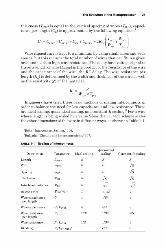
thickness (TINT) is equal to the vertical spacing of wires (TILD), capaci-tance per length (CL) is approximated by the following equation.7
Wire capacitance is kept to a minimum by using small wires and widespaces, but this reduces the total number of wires that can fit in a givenarea and leads to high wire resistance. The delay for a voltage signal totravel a length of wire (LWIRE) is the product of the resistance of the wireand the capacitance of the wire, the RC delay. The wire resistance perlength (RL) is determined by the width and thickness of the wire as wellas the resistivity (r) of the material.
Engineers have tried three basic methods of scaling interconnects inorder to balance the need for low capacitance and low resistance. Theseare ideal scaling, quasi-ideal scaling, and constant-R scaling.8 For a wirewhose length is being scaled by a value S less than 1, each scheme scalesthe other dimensions of the wire in different ways, as shown in Table 1-1.
RW TL
=×ρ
INT INT
C C C C C KT
W
W
TL= + + + ≈ +
LEFT RIGHT UP DOWNINT
SP
INT20
εIILD
The Evolution of the Microprocessor 25
6x9 Technical / Microprocessor Design / McFarland /45951-0 / Chapter 1
7Bohr, “Interconnect Scaling,” 106.8Bakoglu, “Circuits and Interconnections,” 197.
TABLE 1-1 Scaling of Interconnects
Quasi-idealDescription Parameter Ideal scaling scaling Constant-R scaling
Length LWIRE S S S
Width WINT S S
Spacing WSP S S
Thickness TINT S
Interlevel dielectric TILD S
Aspect ratio TINT/WINT 1 1
Wire capacitance CL 1 1/S0.1 1per length
Wire capacitance CL LWIRE S S0.9 S
Wire resistance RL 1/S2 1/S1.5 1/Sper length
Wire resistance RL LWIRE 1/S 1/S0.5 1
RC delay RL CL LWIRE2 1 S0.4 S
1 / S
SS
SS
S
S
951-0 Microproc_CH01.qxd 9/3/06 6:32 PM Page 25
Ideal scaling reduces all the vertical and horizontal dimensions by thesame amount. This keeps the capacitance per length constant butgreatly increases the resistance per length. In the end the reduction inwire capacitance is offset by the increase in wire resistance, and the wiredelay remains constant. Scaling interconnects this way would meanthat as transistors grew faster, processor frequency would quicklybecome limited by the interconnect delay.
To make interconnect delay scale with the transistor delay, constant-Rscaling can be used. By scaling the vertical and horizontal dimensionsof the wire less than its length, the total resistance of the wire is keptconstant. Because the capacitance is reduced at the same rate as idealscaling, the overall RC delay scales with the wire length. The downsideof constant-R scaling is that if S is also scaling the device dimensions,then the area required for wires is not decreasing as quickly as thedevice area. The size of a chip will be rapidly determined not by thenumber of transistors but by the number of wires.
To allow for maximum scaling of die area while mitigating the increasein wire resistance, most manufactures use quasi-ideal scaling. In thisscheme horizontal dimensions are scaled with wire length, but verticaldimensions are scaled more slowly. The capacitance per length increasesonly slightly and the increase in resistance is not as much as ideal scal-ing. Overall the RC delay will decrease although not as much constant-Rscaling. The biggest disadvantage of quasi-ideal scaling is that itincreases the aspect ratio of the wires, the ratio of thickness to width.This scaling has rapidly led to wires in modern processors that are twiceas tall as they are wide, but manufacturing wires with ever-greateraspect ratios is difficult. To help in continuing to reduce interconnectdelays, manufactures have turned to new materials.
In 2000, some semiconductor manufacturers switched from usingaluminum wires, which had been used since the very first integrated cir-cuits, to copper wires. The resistivity of copper is less than aluminumproviding lower resistance wires. Copper had not been used previouslybecause it diffuses very easily through silicon and silicon dioxide. Copperatoms from the wires could quickly spread throughout a chip acting asdefects in the silicon and ruining the transistor behavior. To prevent this,manufacturers coat all sides of the copper wires with materials that actas diffusion barriers. This reduces the cross section of the wire that isactually copper but prevents contamination.
Wire capacitances have been reduced through the use of low-Kdielectrics. Not only the dimensions of the wires determine wire capac-itance but also by the permittivity or K value of the insulator sur-rounding the wires. The best capacitance would be achieved if there weresimply air or vacuum between wires giving a K equal to 1, but of coursethis would provide no physical support. Silicon dioxide is traditionally
26 Chapter One
6x9 Technical / Microprocessor Design / McFarland /45951-0 / Chapter 1
951-0 Microproc_CH01.qxd 9/3/06 6:32 PM Page 26

used, but this has a K value of 4. New materials are being tried toreduce K to 3 or even 2, but these materials tend to be very soft andporous. When heated by high electrical currents the metal wires tendto flex and stretch and soft dielectrics do little to prevent this. Futureinterlevel dielectrics must provide reduced capacitance without sacri-ficing reliability.
One of the common sources of interconnect failures is called electro-migration. In wires with very high current densities, atoms tend to bepushed along the length of the wire in the direction of the flow of elec-trons, like rocks being pushed along a fast moving stream. This phe-nomenon happens more quickly at narrow spots in the wire where thecurrent density is highest. This leads these spots to become more andmore narrow, accelerating the process. Eventually a break in the wire iscreated. Rigid interlevel dielectrics slow this process by preventing thewires from growing in size elsewhere, but the circuit design must makesure not to exceed the current carrying capacity of any one wire.
Despite using new conductor materials and new insulator materials,improvements in the delay of interconnects have continued to trailbehind improvements in transistor delay. One of the ways in whichmicroprocessors designs try to compensate for this is by adding morewiring layers. The lowest levels are produced with the smallest dimen-sions. This allows for a very large number of interconnections. The high-est levels are produced with large widths, spaces, and thickness. Thisallows them to have much less delay at the cost of allowing fewer wiresin the same area.
The different wiring layers connect transistors on a chip the wayroads connect houses in a city. The only interconnect layer that actuallyconnects to a transistor is the first layer deposited, usually called themetal 1 or M1 layer. These are the suburban streets of a city. Becausethey are narrow, traveling on them is slow, but typically they are veryshort. To travel longer distances, wider high speed levels must be used.The top layer wires would be the freeways of the chip. They are used totravel long distances quickly, but they must connect through all thelower slower levels before reaching a specific destination.
There is no real limit to the number of wiring levels that can be added,but each level adds to the cost of processing the wafer. In the end thedesign of the microprocessor itself will have to continue to evolve toallow for the greater importance of interconnect delays.
Microprocessor scaling
Because of the importance of process scaling to processor design, allmicroprocessor designs can be broken down into two basic categories:lead designs and compactions. Lead designs are fundamentally new
The Evolution of the Microprocessor 27
6x9 Technical / Microprocessor Design / McFarland /45951-0 / Chapter 1
951-0 Microproc_CH01.qxd 9/3/06 6:32 PM Page 27
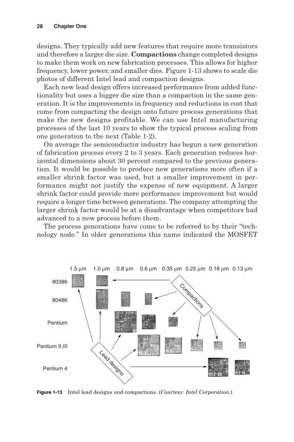
designs. They typically add new features that require more transistorsand therefore a larger die size. Compactions change completed designsto make them work on new fabrication processes. This allows for higherfrequency, lower power, and smaller dies. Figure 1-13 shows to scale diephotos of different Intel lead and compaction designs.
Each new lead design offers increased performance from added func-tionality but uses a bigger die size than a compaction in the same gen-eration. It is the improvements in frequency and reductions in cost thatcome from compacting the design onto future process generations thatmake the new designs profitable. We can use Intel manufacturingprocesses of the last 10 years to show the typical process scaling fromone generation to the next (Table 1-2).
On average the semiconductor industry has begun a new generationof fabrication process every 2 to 3 years. Each generation reduces hor-izontal dimensions about 30 percent compared to the previous genera-tion. It would be possible to produce new generations more often if asmaller shrink factor was used, but a smaller improvement in per-formance might not justify the expense of new equipment. A largershrink factor could provide more performance improvement but wouldrequire a longer time between generations. The company attempting thelarger shrink factor would be at a disadvantage when competitors hadadvanced to a new process before them.
The process generations have come to be referred to by their “tech-nology node.” In older generations this name indicated the MOSFET
28 Chapter One
6x9 Technical / Microprocessor Design / McFarland /45951-0 / Chapter 1
1.5 µm 1.0 µm 0.8 µm 0.6 µm 0.35 µm 0.25 µm 0.18 µm 0.13 µm
Lead designs
Compactions
80386
Pentium
Pentium 4
Pentium II,III
80486
Figure 1-13 Intel lead designs and compactions. (Courtesy: Intel Corporation.)
951-0 Microproc_CH01.qxd 9/3/06 6:32 PM Page 28
gate length of the process (LGATE), but more recently some manufac-tures have scaled their gate lengths more aggressively than others. Thismeans that today two different 90-nm processes may not have the samedevice or interconnect dimensions, and it may be that neither has anyimportant dimension that is actually 90-nm. The technology node hasbecome merely a name describing the order of manufacturing genera-tions and the typical 30 percent scaling of dimensions. The importanthistorical trends in microprocessor fabrication demonstrated by Table 1-2and quasi-ideal interconnect scaling are shown in Table 1-3.
Although it is going from one process generation to the next thatgradually moves the semiconductor industry forward, manufacturers donot stand still for the 2 years between process generations. Small incre-mental improvements are constantly being made to the process thatallow for part of the steady improvement in processor frequency. As aresult, a compaction microprocessor design may first ship at about the
The Evolution of the Microprocessor 29
6x9 Technical / Microprocessor Design / McFarland /45951-0 / Chapter 1
TABLE 1-2 Intel Manufacturing Processes9,10,11,12
Year Technology node (nm) LGATE (nm) TOX-P (nm) Vdd (V) Metal layers
1993 500 500 8.0 3.3 41995 350 350 5.2 2.5 41997 250 200 3.1 1.8 51999 180 130 2.0 1.6 62001 130 70 1.4 1.4 62003 90 50 1.2 1.2 7
9Walden, “90nm and Beyond”10Chau, “Silicon Nano-Transistors.”11Bohr, “Silicon Trends and Limits.”12Bhandarkar, “Billion Transistor Processor Chips.”
TABLE 1-3 Microprocessor Fabrication Historical Trends
New generation every 2 years35% reduction in gate length30% reduction in gate oxide thickness15% reduction in voltage30% reduction in interconnect horizontal dimensions15% reduction in interconnect vertical dimensionsAdd 1 metal layer every other generation
951-0 Microproc_CH01.qxd 9/3/06 6:32 PM Page 29
same frequency as the previous generation, which has been graduallyimproving since its launch.
The motivation for the new compaction is not only the immediatereduction in cost due to a smaller die size, but the potential that it willbe able to eventually scale to frequencies beyond what the previous gen-eration could reach. As an example the 180-nm generation Intel Pentium®
4 began at a maximum frequency of 1.5 GHz and scaled to 2.0 GHz.The 130-nm Pentium 4 started at 2.0 GHz and scaled to 3.4 GHz. The90-nm Pentium 4 started at 3.2 GHz. Each new technology generationis planned to start when the previous generation can no longer be easilyimproved.
The future of Moore’s law
In recent years, the exponential increase with time of almost anyaspect of the semiconductor industry has been referred to as Moore’slaw. Indeed, things like microprocessor frequency, computer perform-ance, the cost of a semiconductor fabrication plant, or the size of amicroprocessor design team have all increased exponentially. No expo-nential trend can continue forever, and this simple fact has led to pre-dictions of the end of Moore’s law for decades. All these predictions haveturned out to be wrong. For 30 years, there have always been seem-ingly insurmountable problems about 10 years in the future. Perhapsone of the most important lessons of Moore’s law is that when billionsof dollars in profits are on the line, incredibly difficult problems canbe overcome.
Moore’s law is of course not a “law” but merely a trend that has beentrue in the past. If it is to remain true in the future, it will be becausethe industry finds it profitable to continue to solve “insurmountable”problems and force Moore’s law to come true. There have already beena number of new fabrication technologies proposed or put into use thatwill help continue Moore’s law through 2015.
Multiple threshold voltages. Increasing the threshold voltage dramati-cally reduces subthreshold leakage. Unfortunately this also reduces theon current of the device and slows switching. By applying differentamounts of dopant to the channels of different transistors, devices withdifferent threshold voltages are made on the same die. When speed isrequired, low VT devices, which are fast but high power, are used. In cir-cuits that do not limit the frequency of the processor, slower, more power-efficient, high VT devices are used to reduce overall leakage power. Thistechnique is already in use in the Intel 90-nm fabrication generation.13
30 Chapter One
6x9 Technical / Microprocessor Design / McFarland /45951-0 / Chapter 1
13Ghani et al., “90nm Logic Technology.”
951-0 Microproc_CH01.qxd 9/3/06 6:32 PM Page 30
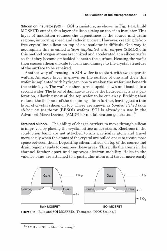
Silicon on insulator (SOI). SOI transistors, as shown in Fig. 1-14, buildMOSFETs out of a thin layer of silicon sitting on top of an insulator. Thislayer of insulation reduces the capacitance of the source and drainregions, improving speed and reducing power. However, creating defect-free crystalline silicon on top of an insulator is difficult. One way toaccomplish this is called silicon implanted with oxygen (SIMOX). Inthis method oxygen atoms are ionized and accelerated at a silicon waferso that they become embedded beneath the surface. Heating the waferthen causes silicon dioxide to form and damage to the crystal structureof the surface to be repaired.
Another way of creating an SOI wafer is to start with two separatewafers. An oxide layer is grown on the surface of one and then thiswafer is implanted with hydrogen ions to weaken the wafer just beneaththe oxide layer. The wafer is then turned upside down and bonded to asecond wafer. The layer of damage caused by the hydrogen acts as a per-foration, allowing most of the top wafer to be cut away. Etching thenreduces the thickness of the remaining silicon further, leaving just a thinlayer of crystal silicon on top. These are known as bonded etched backsilicon on insulator (BESOI) wafers. SOI is already in use in theAdvanced Micro Devices (AMD®) 90-nm fabrication generation.14
Strained silicon. The ability of charge carriers to move through siliconis improved by placing the crystal lattice under strain. Electrons in theconduction band are not attached to any particular atom and travelmore easily when the atoms of the crystal are pulled apart to create morespace between them. Depositing silicon nitride on top of the source anddrain regions tends to compress these areas. This pulls the atoms in thechannel farther apart and improves electron mobility. Holes in thevalence band are attached to a particular atom and travel more easily
The Evolution of the Microprocessor 31
6x9 Technical / Microprocessor Design / McFarland /45951-0 / Chapter 1
14“AMD and 90nm Manufacturing.”
Source Drain
Si
Gate
Bulk MOSFET SOI MOSFET
Gate
Source Drain
SiO2
SiO2
Si
SiO2
Figure 1-14 Bulk and SOI MOSFETs. (Thompson, “MOS Scaling.”)
951-0 Microproc_CH01.qxd 9/3/06 6:32 PM Page 31
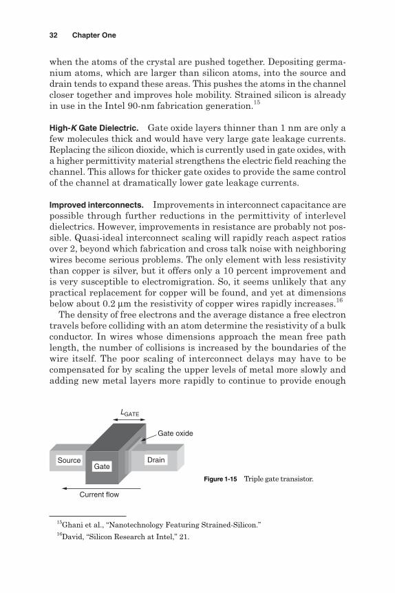
when the atoms of the crystal are pushed together. Depositing germa-nium atoms, which are larger than silicon atoms, into the source anddrain tends to expand these areas. This pushes the atoms in the channelcloser together and improves hole mobility. Strained silicon is alreadyin use in the Intel 90-nm fabrication generation.15
High-K Gate Dielectric. Gate oxide layers thinner than 1 nm are only afew molecules thick and would have very large gate leakage currents.Replacing the silicon dioxide, which is currently used in gate oxides, witha higher permittivity material strengthens the electric field reaching thechannel. This allows for thicker gate oxides to provide the same controlof the channel at dramatically lower gate leakage currents.
Improved interconnects. Improvements in interconnect capacitance arepossible through further reductions in the permittivity of interleveldielectrics. However, improvements in resistance are probably not pos-sible. Quasi-ideal interconnect scaling will rapidly reach aspect ratiosover 2, beyond which fabrication and cross talk noise with neighboringwires become serious problems. The only element with less resistivitythan copper is silver, but it offers only a 10 percent improvement andis very susceptible to electromigration. So, it seems unlikely that anypractical replacement for copper will be found, and yet at dimensionsbelow about 0.2 µm the resistivity of copper wires rapidly increases.16
The density of free electrons and the average distance a free electrontravels before colliding with an atom determine the resistivity of a bulkconductor. In wires whose dimensions approach the mean free pathlength, the number of collisions is increased by the boundaries of thewire itself. The poor scaling of interconnect delays may have to becompensated for by scaling the upper levels of metal more slowly andadding new metal layers more rapidly to continue to provide enough
32 Chapter One
6x9 Technical / Microprocessor Design / McFarland /45951-0 / Chapter 1
Gate oxide
GateSource Drain
LGATE
Current flow
Figure 1-15 Triple gate transistor.
15Ghani et al., “Nanotechnology Featuring Strained-Silicon.”16David, “Silicon Research at Intel,” 21.
951-0 Microproc_CH01.qxd 9/3/06 6:32 PM Page 32
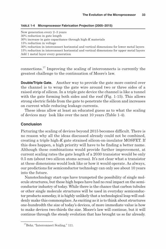
connections.17 Improving the scaling of interconnects is currently thegreatest challenge to the continuation of Moore’s law.
Double/Triple Gate. Another way to provide the gate more control overthe channel is to wrap the gate wire around two or three sides of araised strip of silicon. In a triple gate device the channel is like a tunnelwith the gate forming both sides and the roof (Fig. 1-15). This allowsstrong electric fields from the gate to penetrate the silicon and increaseson current while reducing leakage currents.
These ideas allow at least an educated guess as to what the scalingof devices may look like over the next 10 years (Table 1-4).
Conclusion
Picturing the scaling of devices beyond 2015 becomes difficult. There isno reason why all the ideas discussed already could not be combined,creating a triple high-K gate strained silicon-on-insulator MOSFET. Ifthis does happen, a high priority will have to be finding a better name.Although these combinations would provide further improvement, atcurrent scaling rates the gate length of a 2030 transistor would be only0.5 nm (about two silicon atoms across). It’s not clear what a transistorat these dimensions would look like or how it would operate. As always,our predictions for semiconductor technology can only see about 10 yearsinto the future.
Nanotechnology start-ups have trumpeted the possibility of single mol-ecule structures, but these high hopes have had no real impact on the semi-conductor industry of today. While there is the chance that carbon tubulesor other single molecule structures will be used in everyday semiconduc-tor products someday, it is highly unlikely that a technological leap will sud-denly make this commonplace. As exciting as it is to think about structuresone-hundredth the size of today’s devices, of more immediate value is howto make devices two-thirds the size. Moore’s law will continue, but it willcontinue through the steady evolution that has brought us so far already.
The Evolution of the Microprocessor 33
6x9 Technical / Microprocessor Design / McFarland /45951-0 / Chapter 1
TABLE 1-4 Microprocessor Fabrication Projection (2005–2015)
New generation every 2–3 years30% reduction in gate length30% increase in gate capacitance through high-K materials15% reduction in voltage30% reduction in interconnect horizontal and vertical dimensions for lower metal layers15% reduction in interconnect horizontal and vertical dimensions for upper metal layersAdd 1 metal layer every generation
17Bohr, “Interconnect Scaling,” 111.
951-0 Microproc_CH01.qxd 9/3/06 6:32 PM Page 33

Key Concepts and Terms
Bipolar junction transistor (BJT)
Channel length
Conduction and valence bands
Electrons and holes
Gate oxide
Integrated circuit (IC)
Junction diode
Lead design and compaction
Review Questions
1. What column elements are used as P-type or N-type dopants and why?
2. Describe the valence and conduction bands of a conductor, an insu-lator, and a semiconductor.
3. How is a BJT different than a MOSFET?
4. Why is poly commonly used for MOSFET gates?
5. What are some of the trade-offs in choosing channel length, gateoxide thickness, and threshold voltage?
6. How do microprocessor fabrication processes typically scale over time?
7. In addition to simple scaling what are other fabrication technologiesto improve transistor performance?
8. Why is Moore’s law so important to the semiconductor industry?
9. [Lab] Measure the current versus voltage of a junction diode. Is thecurrent in reverse bias always zero?
10. [Discussion] What are some of the limits to Moore’s law and waysof addressing these limits? How long will Moore’s law continue?How might electronics continue to evolve after Moore’s law?
Bibliography
“AMD and 90nm Manufacturing: Paving the Way for Tomorrow, Today.”http://www.amd.com/us-en/Processors/ComputingSolutions.
Bakoglu, H., Circuits, Interconnections, and Packaging for VLSI, Reading, MA: Addison-Wesley, 1990.
Bhandarkar, Dileep. “Billion Transistor Processor Chips in the Mainstream EnterprisePlatforms of the Future.” Ninth International Symposium on High PerformanceComputer Architecture, Anaheim, CA: 2003.
Bohr, Mark et al. “A High Performance 0.25 µm Logic Technology Optimized for 1.8 VOperation.” International Electronic Devices Meeting, San Francisco, CA: 1996, pp. 847–850.[Describes Intel’s 250-nm process generation.]
Bohr, Mark. “Interconnect Scaling—The Real Limiter to High Performance ULSI.” SolidState Technology, September 1996, pp. 105–111.
34 Chapter One
6x9 Technical / Microprocessor Design / McFarland /45951-0 / Chapter 1
Metal oxide semiconductor field-effecttransistor (MOSFET)
Moore’s law
N-type, P-type
Polycrystalline silicon (Poly)
Silicon on insulator (SOI)
Threshold voltage
951-0 Microproc_CH01.qxd 9/3/06 6:32 PM Page 34
Bohr, Mark. “Silicon Trends and Limits for Advanced Microprocessors.” Communicationsof the ACM, March 1998, pp. 80–87.
Ceruzzi, Paul. A History of Modern Computing. 2d ed., Cambridge, MA: The MIT Press, 2003.Chau, Robert. “Silicon Nano-Transistors and Breaking the 10nm Physical Gate Length
Barrier.” 61st Device Research Conference, Salt Lake City, UT: June 2003.Chen, Gang et al. “Dynamic NBTI of p-MOS Transistors and Its Impact on MOSFET
Scaling.” IEEE Electron Device Letters, San Francisco, CA: 2002.David, Ken. “Silicon Research at Intel.” Global Strategic Forum, Washington DC: March 2004.Dennard, Robert et al. “Design of Ion-Implanted MOSFETs with Very Small Dimensions.”
IEEE Journal of Solid Static Circuits, 1974, pp. 256–268.Einstein, Marcus and James Franklin, “Computer Manufacturing Enters a New Era of
Growth.” Monthly Labor Review, September 1986, pp. 9–16.Flatow, Ira et al. “Transistorized.” ScienCentral Inc. and Twin Cities Public Television, 1998,
http://www.pbs.org/transistor/index.html. [A fun and extremely accessible public televisionspecial on the invention of the transistor. Based mainly on the book Crystal Fire.]
Flynn, Michael and Patrick Hung, “Microprocessor Design Issues: Thoughts on the RoadAhead,” IEEE Computer Society, Los Alamitos, CA: 2005. [A great discussion of theimpact of Moore’s law on design.]
Ghani, Tahir. et al. “A 90nm High Volume Manufacturing Logic Technology FeaturingNovel 45nm Gate Length Strained Silicon CMOS Transistors.” International ElectronicDevices Meeting, Washington DC: 2003. [Describes Intel’s 90-nm process generation.]
Ghani, Tahir. et al. “100nm Gate Length High Performance/Low Power CMOS TransistorStructure.” International Electronic Devices Meeting, Washington DC: 1999, pp. 415–418.[Describes Intel’s 180nm process generation.]
McFarland, Grant. “CMOS Technology Scaling and Its Impact on Cache Delay.” StanfordUniversity PhD Dissertation, 1995. [My own PhD dissertation did a fair job ofpredicting the characteristics of the 90-nm process generation, which was reached 10years later.]
Moore, Gordon. “Cramming More Components onto Integrated Circuits.” Electronics,April 1965, pp. 114–117. [The original paper showing Moore’s law. Predicts a doublingof the number of transistors on a die every year from 1959 to 1975. Moore’s 1975 paperrevised this to a doubling every 18 months.]
Moore, Gordon. “Progress in Digital Integrated Electronics.” International ElectronicDevices Meeting, December 1975, pp. 11–13. [The second and most often quotedformulation of Moore’s law.]
Moore, Gordon. “No Exponential is Forever... But We Can Delay Forever.” InternationalSolid State Circuits Conference, San Francisco, CA: February 2003. [A great update onMoore’s law by the creator himself.]
Muller, Richard and Theodore Kamins. Device Electronics for Integrated Circuits. 2d ed.,New York: John Wiley & Sons, 1986. Real, Mimi. A Revolution in Progress: A History ofIntel to Date. Santa Clara, CA: Intel Corporation, 1984.
Reid, T. R. The Chip, Random House Trade Paperbacks, 2001. [Tells the story of theinvention of the integrated circuit by Jack Kilby and Bob Noyce.]
Riordan, Michael and Lillian Hoddeson. Crystal Fire, New York: W. W. Norton & Company,1997. [Tells the story of the invention of the transistor.]
Roberts, Bruce, Alain Harrus, and Robert Jackson. “Interconnect Metallization for FutureDevice Generations.” Solid State Technology, February 1995, pp. 69–78.
Thompson, Scott et al. “A Logic Nanotechnology Featuring Strained-Silicon.” IEEEElectron Device Letters, April 2004, pp. 191–193. [A description of the strained silicontechnique used in Intel’s 90-nm process generation.]
Thompson, Scott et al. “MOS Scaling: Transistor Challenges for the 21st Century.” IntelTechnology Journal, Q3 1998, pp. 1–19.
Walden, Josh. “90nm and Beyond: Moore’s Law and More.” Intel Developer Forum, SanJose, CA: April 2003.
Walker, Robert et al. “Silicon Genesis: An Oral History of Semiconductor Technology.”http://silicongenesis.stanford.edu. [An incredible collection of interviews with many ofthe founders of silicon valley including Gordon Moore, Ted Hoff, Fedrico Faggin, JerrySanders, and many others.]
The Evolution of the Microprocessor 35
6x9 Technical / Microprocessor Design / McFarland /45951-0 / Chapter 1
951-0 Microproc_CH01.qxd 9/3/06 6:32 PM Page 35

6x9 Technical / Microprocessor Design / McFarland /45951-0 / Chapter 1Blind folio 36
951-0 Microproc_CH01.qxd 9/3/06 6:32 PM Page 36