9 mv*.*- · through factor (i.e., lower doping in the p-layer) is generally desirable for efficient...
TRANSCRIPT

UNCLASSIFIED
AD NUMBER
LIMITATION CHANGESTO:
FROM:
AUTHORITY
THIS PAGE IS UNCLASSIFIED
ADB020021
Approved for public release; distribution isunlimited.
Distribution authorized to U.S. Gov't. agenciesonly; Test and Evaluation; 09 JUN 1977. Otherrequests shall be referred to ElectronicSystems Division, ATTN: EDS/TML, Hanscom AFB,MA 01731.
AFGL ltr dtd 2 May 1985

^T5^"*^ _ ■
. . ,. ,
AD /
9 V*.*- '
■A>m
•k* * .-i^;: .^L.....i
»
AUT • —
L'
r. •

lPWjjiJi!,ws,*ia'v ■'■■■■■ ■ ■ ■-■'j^'wwiwfl'j^j.f^i'iwj'i
\
ESD-TR-77-30
♦
o o o CQ
■EC
CO
■ —It
^ csa
riMü.
Technical Report
Theory and Operating Characteristics
of TRAPATT Amplifiers
524 /
;R. W. Laton
G. I. Haddad
M. I. Grace
26 January 1977
Prepared for the Ballistic Missile Defense Program Office, Department of the Army, ?
under Electronic Systems Division Contract F19628-76-C-0002 by
Lincoln Laboratory MASSACHUSETTS INSTITUTE OF TECHNOLOGY
LEXINGTON, MASSACHUSETTS
Distribution limited to U.S. Government agencies only; test and evaluation; 9 June 1977, Other requests for this document must be referred to ESD/TML (Lincoln Laboratory), Hanscom AFB, MA 01731.

The work reported in this document was performed at Lincoln Laboratory, a center for research operated by Massachusetts Institute of Technology. This program is sponsored by the Ballistic Missile Defense Program Office, Department of the Army; it is supported by the Ballistic Missile Defense Advanced Technology Center under Air Force Contract F19628-76-C-0002.
This report may be reproduced to satisfy needs of U.S. Government agencies.
The views and conclusions contained in this document are those of the contractor and should not be interpreted as necessarily representing the official policies, either expressed or implied, of the United States Government.
This technical report has been reviewed and is approved for publication.
FOR THE COMMANDER
Ray<toond L. Loiselle, Lt. Col., USAF Chief, E3D Lincoln Laboratory Project Office
Non-Lincoln Recipients
PLEASE DO NOT RETURN
Permission is given to destroy this document when it is no longer needed.

liilllBIIPIWMMMfPPPiWWBffff"' ' ^^^-MU■|^^^^ll|■BW^I■■l^■l■ll^^
MASSACHUSETTS INSTITUTE OF TECHNOLOGY
LINCOLN LABORATORY
THEORY AND OPERATING CHARACTERISTICS OF TRAPATT AMPLIFIERS
R. W. LATON
Group 33
G. I. HADDAD, Consultant
Univeraity of Michigan
M. I. GRACE, Consultant
Teledyne M.E.C.
TECHNICAL REPORT 524
26 JANUARY 1977
Distribution limited to U.S. Government agencies only; test and evaluation; 9 June 1977. Other requests for this document must be referred to ESD/TML (Lincoln Laboratory), Hanscom AFB, MA 01731.
LEXINGTON / MASSACHUSETTS
,.■■;-.,„.,i^^;».^,,:.r.w:,:.^,:,.^^^

JkmfMWWMWIWIIJBM^^ "^ ^
I
ABSTRACT
This report describes the current state of understanding of the theory and operating characteristics of microwave avalanche diodes operating
in the TRAPATT mode as both oscillators and amplifiers. Device op-
erating principles, and their dependence upon material, impurity pro-
file, structure, biasing, ana circuit loading are described. Methods of device fabrication are discussed, and present state of the art is
tabulated for oscillators and amplifiers on a power-frequency basis.
Techniques developed for the design of TRAPATT amplifiers as a re- sult of several programs sponsored by the U.S. Army Ballistic Missile
Defense Advanced Technology Center are discussed, and experimental
results (primarily at S-band) are presented.
yf i
■■n<miH«w^-*"tr-i>!rxi!»[
csDim Pioi^iwc-i^ jriiMtp,
iii
HL ■jjaaAasaaiite^^^

Imt W! h'' «V.l'. ■ ' '"" ' ' ." . "i .i
CONTENT S
II.
III.
IV.
Abstract
HISTORICAL BACKGROUND
A. Introduction
B. Discovery and Description of the IMPATT Mode
C. Discovery of the High-Efficiency Mode
THEORY OF DEVICE OPERATION
A. Basic Operating Principles
B. Approximate Analysis
C. Harmonic Effects
D. Initiation of the TRAPATT Mode
DEVICE DESIGN AND PRODUCTION
A. Introduction
B. Fabrication of Etched-Mesa Devices
C. Distributed Area Cross-Section Devices
D. Junction Formation
E. Planar-Type Devices
STATE OF THE ART
A. TRAPATT Oscillators
B. TRAPATT Amplifiers
AMPLIFIER DESIGN PRINCIPLES
A. Introduction
B. TRAPATT Oscillators and Amplifiers
C. Carroll Theory for TRAPATT Amplifiers
1. Introduction 2. Admittance Characteristics for TRAPATT Amplifiers
D. Wideband Amplifier Circuits
1. General Circuit Conditions 2. Coupled-Line Amplifier Circuit 3. Lumped-Element Circuits
E. Harmonic Effects
iii
1
1
i
2
5
5
8
11
12
15
15
15
16
17
19
21
21
21
25
25
25
27
27 29
31
31 32 37
40
iv
Nkii6faiAitia^M*JJ.J^.v-.:.,.^^..fc-.

i
VI. EXPERIMENTAL RESULTS
A. Introduction
B. Coupled-Line Amplifiers C. Experimental Large Area Diode Amplifiers
Using Lumped-Element Circuits
D. Dependence on Output Load
E. Lincoln Measurements 1. Lincoln Measurements on the Sperry 50-W
Lumped-Element Amplifier
2. A Fixed-Tuned TRAPATT Amplifier Synthesis Procedure
VE. SUMMARY AND CONCLUSIONS
APPENDIX - Government Contract Reports
References
43
43
43
49 51
56
61
63
65
]
! V
1 1 ■HHHHttiMIJttttlMttWiUM ^-.■-..-..-. ^.-■ .^ ..•■,..-...,,t^^^^äüStiiiäiiäti^M .;l^
;,l^..*.'.[^^-., ^.

THEORY AND OPERATING CHARACTERISTICS OF TRAPATT AMPLIFIERS
CHAPTER I HISTORICAL BACKGROUND
1
i |
■
1
A. INTRODUCTION
The purpose of this report is to document the present state of understanding of the theory and operating characteristics of TRAPATT diodes. The discovery of this mode of oscillation in solid-state devices in the late 1960's generated interest and support on the part of the Bal- listic Missile Defense (BMD) technology development community, since peak power levels, ef- ficiencies, and operating frequencies of these devices are compatible with requirements for S-band phased-array-radar power amplifiers.
This chapter discusses the discovery of the TRAPATT phenomena in a historical sense,
and relates it to transit-time negative resistance and the IMPATT diode of Shockley1 and Read, respectively.
Chapters II through IV then develop the theoretical concepts responsible for the operation of the device, describe various methods available for its fabrication, and tabulate the present
oscillator and amplifier state of the art. Chapters V and VI discuss techniques for the design of TRAPATT amplifiers and provide
experimental results which are characteristic of the best of those which have been constructed.
Chapter VII summarizes this report and provides conclusions and further recommendations,
and the Appendix presents a bibliography of Government Contract Reports available from the
National Technical Information Service (NTIS) concerning TRAPATT generation and amplifica-
tion of microwave power.
B. DISCOVERY AND DESCRIPTION OF THE IMPATT MODE
The negative resistance arising from the transit time of charge carriers in semiconductor 1
devices was first considered by Shockley in 1954. The device proposed by Shockley was a pnp
structure in which charge carriers are injected at one of the p-n junctions and drift through the
n-region to the opposite junction. Because a finite time is required for the particles to traverse
the structure, the terminal current induced by the moving charge carriers lags the terminal volt- age by the transit time of the injected particles. For appropriate frequencies, the phase dif- ference between the terminal current and voltage remains between 90° and 270°. Therefore,
the device exhibits a negative resistance and is capable of generating RF power. Shockley pro- posed that these devices be used as amplifiers.
A diode structure in which the phase lag between the terminal current and voltage is achieved by both: (1) generation of charge carriers through impact ionization, and (2) the transit time of
2 -t + these carriers, was proposed by Read in 1958. The structure proposed by Read was an n'pip
diode in which the electric field at the n p junction would be large enough to allow charge mul- tiplication by impact ionization. (Throughout this report, the 4 superscript refers to a highly doped, or low-resistivity region of semiconductor material.) The p-region is made narrow so
that most of the chai ge multiplication occurs at the n p interface. The electric field in the
|p^ .1 it-MWBuiiMUjm,,. M^ j.
4 v''""
Wim PAOi^fciMK-NOT flÜBD. 'Sfan "liifiM ' -• -;',J'r^?-J'^?*'^'lllt!l!!i^!)llllll«tl,]■.r, ^

wmmm^misf^.j^^'iwwmm'mmmma
i:-.
Fig. 1-1. IMPATT mode waveforms.
0 180 360
PHASE ANGLE (dig)
intrinsic region is not large enough to sustain avalanche multiplication but is high enough so that
the injected charge carriers travel at field-independent, saturated velocities. The avalanche
multiplication process contributes a 90° inductive phase lag to the terminal current-voltage
waveforms (e.g., see Fig. 1-1) and the transit time of the charge carriers contributes an addi-
tional phase delay so that the current induced in the external circuit lags the voltage by a phase
angle between 90'' and 270*. The device, therefore, produces a negative resistance. Read
showed theoretically that the device was capable of producing high-power microwave oscilla-
tions with efficiencies of 30 percent. This mode of oscillation was given the acronym IMPATT
mode (impact ionization avalanche transit time) and has been discussed extensively in the litera- ture. Experimentally, IMPATT oscillations have been observed in both p-n junction diodes and
Read-type structures. Diodes operating in the IMPATT mode usually have a cutoff frequency,
below which the phase delay of the current relative to the voltage is less than 90" and, therefore,
the diode does not possess negative resistance. Typical power levels and efficiencies for this mode of operation are generally less than 3 or 4 W at X-band, and 10- to 15- percent efficiency
3 for the simpler p-n junction diodes, and up to 37-percent efficiency for structures similar to
that proposed by Read.
C. DISCOVERY OF THE HIGH-EFFICIENCY MODE 4
In 1967, Prager et aL, while using Si avalanche diode oscillators, observed a new high-
efficiency mode of operation that differed considerably from the usual IMPATT operation. The new mode was characterized by efficient DC-to-RF conversions (up to 60 percent), operation
at frequencies well below the IMPATT transit-time cutoff frequency, and a significant change
MiiMÜM iäiÄai^___ HMi --■" ' -■*'

■•—-
in the DC voltage when the diode switched into the mode. Since this new mode did not obey the
IMPATT explanations they called their discovery the "anomalous mode." In 1968, Scharfetter et al. proposed a mechanism for this new mode which they called the
TRAPATT mode (an acronym for trapped plasma avalanche triggered transit). Their explana-
tion was based on a detailed computer simulation of an avalanche diode and showed the forma-
tion of a moving avalanche zone and trapped plasma. Based on the computer results, DeLoach
and Scharfetter proposed a simplified analysis of the device physics of the TRAPATT mode
mechanism. A similar explanation was offered at approximately the same time by Clorfeine
et al. The simplified analyses usually proceed by assuming a particular current waveform
across the diode (e.g., a square wave) and then calculating the corresponding voltage waveform from the device physics. A Fourier analysis of the waveforms is then performed so that impe-
dances, efficiencies, and other important operating parameters of the device can be calculated.
'■fl
j'J ■
;v! ■■'■■ i
K i
;,,' 1
r
1
I 1 | 1 1
1 3 ■|
Ifeii m .,,-,...,.... _,_.___ ..

CHAPTER II
THEORY OF DEVICE OPERATION
A. BASIC OPERATING PRINCIPLES
The diodes used for TRAPATT mode applications can have a variety of doping profiles including the n+pp+, n+npp+, or p+nn+ structures. When reverse biased into avalanche break-
down, these have doping and electric field profiles similar to that shown in Fig. II-1 for the
n+pp+ diode. In contrast to most IMPATT devices, the diodes used for TRAPATT mode applica- tions are "punched through" under reverse bias and, thus, the whole lightly doped region is
depleted of carriers. Any undepleted region is undesirable because it acts as a series resistance
to the diode and although it has a stabilizing effect on oscillator performance, it has a strong degrading effect on the oscillator RF power and efficiency. As will be seen later, a high punch-
through factor (i.e., lower doping in the p-layer) is generally desirable for efficient TRAPATT
operation. For an understanding of the operating principles of the TRAPATT mode, it is useful to as-
sume a square-wave terminal current through the diode so that a constant amplitude current
with a relatively high magnitude flows for one-half the RF cycle and a constant amplitude cur-
rent with a low magnitude flows for the second half of the RF cycle. The current flowing through
|1I-M»345|
Fig. II-l. TRAPATT diode impurity density and electric field profiles.
* o >■
£ E S
I
n* p P*
1 i p-TYPE
n-TYPE
1
E,
DISTANCE
L ^pafllPR^^ "'4-~
,,,.
„ . . . ..- : i_^_ -:-:..:..:.,.;_:,_ „_ ,,.~r;,:;_ui^ia^ititjal..ji.^!iö_.ii;i^ ^.„.^^w,.:;:^.:,:.:. .:„:.;. i,,.':*

< z i a ui
160 iU-MI3U| 1
120 SILICON P-Z-8-0 OIODE
" f\ JTO •'lOO.OA/em2 j / 1 JT • 20.0 M/cm2 | / 1 FREQUENCY ■ 4,630GHi j
BO i |
40 1 J 0 x—i i i 1
90 180 270
PHASE ANGLE (<)•«)
Fig. II-2. TRAPATT diode terminal waveforms.
360
0.9 10 1.9 20
DISTANCE (/im) 0 0 5 10 1.9 20
DISTANCE (Mm)
PHASE=165°
■ ELECTRIC FIELD
HOLE DENSITY
ELECTRON DENSITY
0 0,5 10 19 20
DISTANCE Ipm)
(f) (d) (•)
Fig. II-3. TRAPATT profiles during oscillation cycle.
■■ -'-- ^^~-~~-^.. ^^- ~^^*.

*»pw,*i[ww^^ f!^^y-V7-^F *F®W*'?FWS!ffi^'sWWS
J.
I
the diode during the second half of the cycle or "off" period can be considered to be the reverse
saturation current in this situation. The terminal voltage and current waveforms under these
conditions are illustrated in Fig. II-2. The internal dynamics of the TRAPATT mode are illustrated in Figs.II-3(a-f) for selected
times during the first half of the RF cycle.
Initially, the diode voltage is assumed to be just below the breakdown value so that only a
small reverse saturation conduction current Jc flows. The constant magnitude terminal current J_ is suddenly applied, causing a displacement current to charge the diode as a linear capacitor
(Fig. II-3(a)]. Under these conditions the terminal current is primarily composed of that dis-
placement current. As the diode charges, the voltage rises in proportion to the integral of the
terminal current and when the voltage becomes larger than the breakdown value, an electron- hole plasma is generated in the diode (Fig. II-3(b)]. This process continues until enough charge
has been generated so that the terminal current is entirely composed of conduction current.
The space charge from the generated carriers is sufficient to force the electric field on the
right of the avalanche zone to a high enough value so that additional charge carriers are gener-
ated. As this occurs, a "shock front" or traveling avalanche zone is created in which the elec-
tric field to the right of the zone is increased above the breakdown field and a dense electron-
hole plasma is left in the "wake" of the traveling zone [Fig. II-3(c)]. The electron-hole plasma
reduces the electric field behind the avalanche zone to a small value. The avalanche zone prop- agates rapidly so that the electron-hole plasma, which now drifts at low, electric-field-dependent
velocities, is not able to catch up. As a result, the diode is filled with the trapped plasma and
the terminal voltage is reduced to a minimum value [Fig. II-3(d)l. Since the terminal current is maintained at a constant value, the plasma 's drained from the
diode at low, field-dependent velocities. The holes drift to the right toward the p -contact and
the electrons to the left toward the n -contact. As the charge carriers are drained from the re- gions adjacent to the highly doped contacts, the electric field in these regions begins to recover
and increase in magnitude [Fig. II-3(e)]. This process continues until the diode is completely
drained of mobile charge carriers [Fig. II-3(f)]. The diode again acts as a linear capacitor and
the voltage increases in proportion to the integral of the terminal current. This process con- tinues until the diode terminal voltage reaches a value just below the breakdown condition and the half-cycle is complete. A Fourier analysis now can be made on the terminal current and
voltage waveforms to determine RF power, efficiency, impedances, etc.
High efficiencies are possible with the TRAPATT mode because the RF cycle consists of a high-current low-voltage condition for the first half of the RF period and a high-voltage low-
current condition for the second half of the RF period. The diode, simply stated, acts as a
microwave switch. It should be clear from the current and voltage waveforms that the operating voltage in the
TRAPATT mode is much lower than the breakdown voltage of the device. It has been observed
that, in general, the lower the operating voltage relative to the breakdown voltage, the more
efficient the device will be. The waveforms shown in Figs.II-2 and -3 represent the final steady-state oscillations in
9 10 the device. They were obtained from a computer analysis developed by Lee £t alj ' and re- H suits on various types of structures based on this analysis are given elsewhere.
12 This analysis assumes a square current waveform, which Bryant and Welch have shown
is not accurate since it requires power to be supplied to the diode at higher harmonics of the
mm «^ MliliSiiMMilftliaifiilliMi ^_,_ ^^.-.■^.,^...^.-,
—-.•-■. ..■-■-:. ■ ..

■IMMWmillWIIIMTlWilWWWWWIIWllllllll^ IP I ll l|iiHii|ll|iii|l
- ^-, .*<-. ^ »-X, «...rfr- . ■-—
13 14 oscillator waveform. Other analyses ' reveal that high-efficiency waveforms do exist which
satisfy requirements for trapped plasma formation and field-dependent extraction without a re-
quirement for active harmonic terminations. The analysis does contain the appropriate semi-
conductor physics constraints, and is believed to provide an accurate basis for comparing dif- ferent device structures and materials.
Finally, transient starting mechanisms for the TRAPATT mode are discussed in Sec. D.
—» -*
B. APPROXIMATE ANALYSIS
Several simple approximate analyses exist, which provide basic information concerning
the device principles and properties. One of these has been presented by Haddad et aL,15 based
on previous work done by Schroeder and Haddad (avalanche-region width). Evans17 (approxi- mate expression for the delay time and overvoltage), and DeLoach and Scharfetter7 (recovery
time after the initiation of the dense plasma). Most of the important features of the TRAPATT mode can be readily seen from this model.
|lB-3-19346|
« ' TIME
(a) Fig. II-4(a-b). Approximate current and voltage waveforms.
o <
TIME
(b)
In this analysis the terminal current of the diode is assumed to have the waveform shown in
Fig. II-4(a), and the corresponding terminal voltage is approximated by the waveform shown in Fig. II-4(b) where
t j = delay time
t = recovery time
t = diode charging time
aaiaat^^eiiBMM^jg.,;^^.

mmaixmB^mmvfmfinmmEymmmmmmi&Fvai!.'- ... . ^—— i i i ————T
'X. on "dn^^ime fc #-*
toff = "off" time.
..
The diode terminal voltage at the beginning of the cycle is chosen to be the diode DC breakdown
voltage V-r,. The "on" time t is chosen to be t = t, + t + t. and the "off" time t „ is 6 B on on a p c off chosen to be equal to t^. The waveform shown in Fig. II-4 is idealized but gives reasonable re-
Since t is assumed on 7.8,12
suits at the fundamental frequency and has been employed by others
to equal t .-, the fundamental frequency is given by f = l/2t .
For the analysis, the breakdown voltage VT, and the avalanche region width w for a partic-
ular diode structure are obtained as described by Schroeder and Haddad. Then the delay time 17
t, and the peak voltage V are calculated by solving Evans equations which are given by
V^l'^i'a^^)] (II-1)
and
wJ V_ VB + (II-2)
where X = the constant in a = A exp[XE]. For silicon, the value of X has been chosen to be
0.333 X 10"5 cm/V,
J = total current density during the first half-cycle,
J = reverse saturation current density (a value of 1 A/cm is taken
for J in this study), s
w = avalanche region width, defined as the width where the majority
particle current density reaches 85 percent of the total current
density when the diode is reverse biased into breakdown.
w
v_
diode width, and
saturated drift velocities of carriers (v is assumed to be
1 x 10 cm/sec in this study).
The recovery time t is obtained by using DeLoach and Scharfetter's equation
t = =^ P Zvn 2v. (II-3)
where
"s J (11-4)
and J is obtained by solving
J rJ i
^=expra • (II-5)
._^_^ . : ^ - ,■■ .-.-

a^TOw^gaiiH^nKr--::-. .L :j^izmsmBmammmBEmmmssst
-ä tZ-y. *f <- *- ••■
-**,— ♦ • - - •• r-^— - ^ «•- ••.-<!» ^ •'^^
10 nio
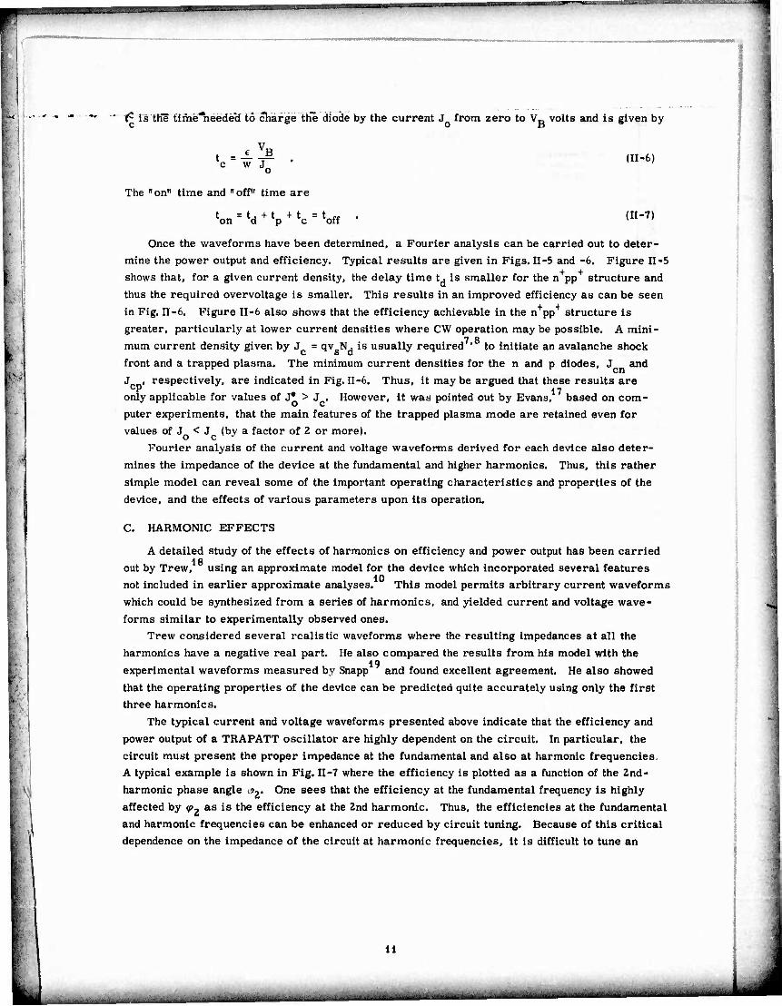
Fig. II-5. Dependence of power, frequency, and delay time on current density for n- and p-type diodes.
Fig. II-6. Dependence of efficiency and overvoltage on current density for n- and p-type diodes.
10
^ ki
^\ :.aE3BEJHi~Bm'Tiiiiiiii I. iiiwiim "i ■■" IIIIIIIHIIII—TI -r-r
'"*• ' £*- is tKe fifhe^ieedeH to charge the diode by the current J from zero to VR volts and is given by B
w J„ (II-6)
The "on" time and "off" time are
t =t, +t +t =t„ on d p c off (II-7)
Once the waveforms have been determined, a Fourier analysis can be carried out to deter- mine the power output and efficiency. Typical results are given in Figs. II-5 and -6. Figure II-5
shows that, for a given current density, the delay time t, is smaller for the n pp structure and
thus the required overvoltage is smaller. This results in an improved efficiency as can be seen
in Fig. II-6. Figure II-6 also shows that the efficiency achievable in the n pp structure is
greater, particularly at lower current densities where CW operation maybe possible. A mini- 7 8 mum current density giver by J = qv N , is usually required ' to initiate an avalanche shock
front and a trapped plasma. The minimum current densities for the n and p diodes, J and
J , respectively, are indicated in Fig. II-6. Thus, it may be argued that these results are CP 17 only applicable for values of J* > J . However, it was pointed out by Evans, based on com-
puter experiments, that the main features of the trapped plasma mode are retained even for values of J < J (by a factor of 2 or more).
Fourier analysis of the current and voltage waveforms derived for each device also deter-
mines the impedance of the device at the fundamental and higher harmonics. Thus, this rather
simple model can reveal some of the important operating characteristics and properties of the
device, and the effects of various parameters upon its operation.
C. HARMONIC EFFECTS
A detailed study of the effects of harmonics on efficiency and power output has been carried 18 out by Trew, using an approximate model for the device which incorporated several features
not included in earlier approximate analyses. This model permits arbitrary current waveforms
which could be synthesized from a series of harmonics, and yielded current and voltage wave-
forms similar to experimentally observed ones. Trew considered several realistic waveforms where the resulting impedances at all the
harmonics have a negative real part. He also compared the results from his model with the 19 experimental waveforms measured by Snapp and found excellent agreement. He also showed
that the operating properties of the device can be predicted quite accurately using only the first three harmonics.
The typical current and voltage waveforms presented above indicate that the efficiency and
power output of a TRAPATT oscillator are highly dependent on the circuit. In particular, the circuit must present the proper impedance at the fundamental and also at harmonic frequencies. A typical example is shown in Fig. II-7 where the efficiency is plotted as a function of the 2nd-
harmonic phase angle <»,• One sees that the efficiency at the fundamental frequency is highly
affected by </», as is the efficiency at the 2nd harmonic. Thus, the efficiencies at the fundamental
and harmonic frequencies can be enhanced or reduced by circuit tuning. Because of this critical
dependence on the impedance of the circuit at harmonic frequencies, it is difficult to tune an
11
MMm.i-il.Mi.ifiiiin *■■-■■ ■ ^^.^Ma^^,,,^^^^. Uidt^a^Ma •-' - ""'"—^

f "■■■'l^M^F^WWWIWWWTF^WIff^Pl'™»Wff»rTfrTf^^"t"ffJ»''»'-^T!'-" 'J -
At 1 ... 1 |U-J-19J49|
40 FUNDAMENTAL \ 2tid HARMONIC y 1 3rd HARMONIC /
M y/ 1 l /^ >- 24
i u b. Si «
' \y •
1 0 ^Z.
Fig. II-7. Relationship between efficiency and phase of 2nd-harmonic voltage.
240 iSO
PHASE ANGLE ^2 (d«g)
oscillator continuously over a broad frequency range and maintain a constant power output and
efficiency. This creates many problems in the broadbanding of TRAPATT amplifiers as will be
discussed in Chaps. V and VI.
D. INITIATION OF THE TRAPATT MODE
The initiation of the TRAPATT mode is complex and not completely understood at this time.
Several mechanisms are generally believed to be involved in the initiation of this mode of oper- ation, and are discussed briefly here.
Many oscillators exhibit a small-signal negative conductance at the operating frequency.
Thus, when such devices are placed in a proper circuit, oscillations will build up to a steady-
state value which is determined by the circuit and the nonlinear behavior of the device. For stable oscillators, the negative conductance decreases with the amplitude of the oscillation and reaches a steady-state value equal to the circuit conductance.
TRAPATT oscillations are different in that the device does not always exhibit a small-signal
negative conductance at the TRAPATT frequency, although in some instances one may exist. The initiation of the TRAPATT mode is believed to come about from a combination of the follow- ing interdependent factors;
(1) Oscillations at the IMPATT frequency which start because of the inherent negative conductance of the device in the IMPATT frequency range;
(2) The static DC I-V characteristic of the device which is highly dependent
on the doping profile and the magnitude of the DC current. In many in-
stances, the DC I-V characteristic exhibits a negative resistance which in turn can lead to bias-circuit oscillations or relaxation-type oscillators;
(3) The dynamic DC I-V characteristic of a device, which is affected by the
magnitude of RF oscillation at the IMPATT frequency;
12
^ ■a'»B»^>ifla"*a*«''kB«fi mmmmmääummä 't^Mi^S^SMimii^Siääm^m^äimäaaläl^iimi ^.. ' .
liMlimWWlMIIIIIIMW^^^WMimMmiiiMi^^ 'v-^'' - , .F~~^r2zz-
(4) Parametric-type interactions in the device which can result in a negative
resistance at lower frequencies;
(5) The rise time of the applied current pulse.
One or all these mechanisms in combination can lead to the overvoltage necessary to initiate
the TRAPATT mode. Depending on the type of mechanism involved, the initiation time required
will vary significantly. Finally, bias circuit design is important in TRAPATT circuits since some of these mechanisms can also contribute to diode burnout and spurious oscillations, or
20 noise. All these mechanisms have been observed experimentally.
The following discussion is limited to p+nn+ and n+pp+ devices with uniform doping in the
n and p layers, respectively, but can be extended to other structures.
(1) The DC I-V characteristic in the absence of RF oscillation will exhibit
a negative resistance at a certain critical current density, which de-
pends on the doping in the n and p layer in a direct relationship. For example, the critical current density for a p -i-n structure is essen-
(2)
tially zero.
For comparable doping levels, the critical current density for p nn
devices is smaller than for n pp ones.
For both devices, the DC negative resistance increases with current
density, beyond the critical value.
For both devices, the critical current density decreases as the ampli-
tude of the RF oscillation at the IMPATT frequency increases.
Fig. II-8 demonstrates some of these effects.
(3)
(4)
i
3 -
I 2
|U-}-H580|
100 190
Fig. II-8. Dynamic current-volt age characteristics of p- and n-type diodes.
13
i..,aa«^MM,.iittaaa^^ ■^^jM^UiMM* ■ ■INI III I**» ■^"-^--

lÄTlHsSSÜBE
As a result, some of the ways the TRAPATT mode can be initiated are:
(1) If the device I-V characteristic does not exhibit a DC negative resistance even in the presence of RP IMPATT oscillations, then the initiation mech-
anism will depend on IMPATT oscillations alone. In this case, the proper
circuit impedance at the IMPATT frequency can cause the RF oscillations
to build up to a large-enough amplitude to initiate the TRAPATT mode. Since p-type devices have a larger small-signal negative conductance than
n-type ones, the starting current and the time for initiation of the TRAPATT
mode will be lower for the former device.
(2) Some devices do not exhibit a DC negative resistance in the absence of RF
IMPATT oscillations. As the IMPATT oscillations build up, however,
many devices will start exhibiting a DC negative resistance and will have a negative resistance over a wide range of low frequencies. This can then
result in bias-circuit oscillations, or in relaxation-type oscillations which
lead to the overvoltage required to initiate the TRAPATT mode. In this case, n- and p-type devices may be comparable. However, if the bias circuit is not properly designed, the n-type devices may be more sus-
ceptible to burnout and the power output and efficiency which may be 18 achieved can be higher for p-type devices.
(3) If the device exhibits a DC negative resistance in the absence of RF oscil-
lations, then the TRAPATT mode can be initiated from bias-circuit
relaxation-type oscillations without requiring any IMPATT oscillations. In
this case, the starting current and the time for initiation will be lower for
the n-type device. Again, careful bias-circuit design is necessary to
prevent burnout.
(4) Another phenomenon which has been observed is related to the rise time
of the bias-current pulse. If this rise time is very short, reflections in
the circuit can lead to a high-enough voltage to initiate the TRAPATT mode.
All these effects also appear in TRAPATT amplifiers. However, since a large RF input
signal is applied, this input signal itself can lead to initiation of the mode.
Some of the effects discussed above have been observed in a device-circuit interaction 20 simulation program. That work is continuing and may provide further insight into the oper-
ation of TRAPATT devices.
14
--'—"-■i"a-»*- L_. , 2M^'mMikMsi^mBsMmtii ^....a^amüafa, - -.■.--■■- -^...w.^..-

s^^TZ?^r^^rTT-'v^T'i^^T^j^ j, __ . ^_
■'■■■ ■ ,:>:-
CHAPTER III
DEVICE DESIGN AND PRODUCTION
INTRODUCTION
There are a number of structures and methods currently in use for the fabrication of
TRAPATT diodes, and this chapter is intended to review and compare the properties of the most
important of these. It is not intended as a description of all the technological details which per-
tain to the production of devices.
TRAPATT oscillations have never been observed in GaAs, for reasons which are not pres-
ently understood. Thus, fabrication of these devices makes use of silicon technology, which
is a relatively mature art. Differences between devices are largely those of: polarity (p- or
n-type doping in the depletion region); type and depth of junction (deep or shallow diffused, shal- low implanted, or surface Schottky barrier); direction of current flow [planar or vertical (mesa)
orientation]; and cross-sectional classifications such as lumped or distributed area devices. Choices among these are driven by considerations of expected RF properties, available tech-
nology, passivation against surface effects, and thermal impedances. These will be discussed
in detail in the following sections.
B. FABRICATION OF ETCHED-MESA DEVICES
The early history of the TRAPATT mode's discovery and investigation may be considered
as an evolutionary perturbation on the broader development of solid-state microwave diodes.
Thus, early fabrication techniques were very similar for both TRAPATT and IMPATT diodes,
while the latter, in turn, closely resembled varactors and pin switching diodes. The etched-
mesa structure has been commonly used for all of these. It is, therefore, important in a his- torical sense and is, as well, currently in use in a great number of these devices. It is also
quite suitable for the tutorial purpose of illustrating the fabrication procedure.
The process begins with a wafer of low-resistivity semiconductor substrate upon which a
thin layer has been grown (usually by either vapor or liquid-phase epitaxial growth techniques)
with the proper doping concentration for the desired device. The substrate is then thinned by mechanical abrasion and/or chemical etching, in order to reduce series resistance in the com-
pleted device. After appropriate cleaning, surface resistivity measurements, and epitaxial
thickness verification, a semiconductor junction is formed near the surface of the epitaxial
layer. Diffusion or ion implantation of appropriate dopants might be used or, alternatively,
Schottky barrier metallizations might be applied. After contact metallizations are in place on
both sides of the wafer, photolithographic techniques are utilized to define the individual diodes,
and the unwanted metal and semiconductor materials are removed from between the mesas by
chemical etching.
Early attempts to increase the permissible current density in both TRAPATT and IMPATT diodes led to the so-called flip-chip structure, in which the completed mesa was bonded upside
down in the package in an attempt to place the junction in close contact with the heat sink. While
this resulted in improved power-handling capability, it was very difficult to obtain a good uni-
form thermal compression bond under the entire mesa because of surface nonuniformity, etc.,
and devices sometimes failed due to localized heating, and technology currently favors a mesa
device with a heat sink plated integrally on the junction side of the device. This technique has
^jB^^^^^Wj^g^^M
15
, ^

m * ■*■-
CONTACT METALLIZATION «
LAYERS
SILICON PHOTORESIST
smmnL. >ww/w\ (c)
Fig. III-l. Fabrication of plated heat-sink mesa diodes: (a) wafer cross section after metallization etch, (b) mesa after etch, and (c) single device after separation etch.
the additional advantage th&t the heat sink is massive enough to permit easy handling of the sep- arate diodes.
Figure III-l illustrates several of these processing steps for the case of a diffused p+nn+
silicon diode.
For pulsed TRAPATT devices, a so-called heat capacitor consisting of a mass of copper
soldered to the substrate side of the device has proven useful in extending the maximum pulse
length before a given temperature rise occurs. The heat absorbed by the heat capacitor then flows out through the device during the "off" time between pulses.
There have been efforts to mount both IMPATT and TR ^PATT devices on diamond heat 22 23
sinks, ' since type Il-a diamond has a thermal conductivity about 3 to 5 times that of copper.
This technique is unquestionably very effective in reducing the spreading component of the
thermal resistance; but, to date, has not found widespread application most likely because of cost and added fabrication complexity.
C. DISTRIBUTED AREA CROSS-SECTION DEVICES
The thermal resistance of large area diodes is dominated by the spreading resistance in the
heat sink, so that attempts to increase the diodes' power-handling capability have led to cross-
sectional shapes with large ratios of periphery to enclosed area. Stripes, annulus shapes, and
arrays of separated smaller diodes are some of these. At RCA, a variation of the multiple-
stripe diode called a cruciform structure combines several desirable properties such as a high
ratio of periphery to enclosed area, a good geometry for uniformity of current distribution, and
16

t^i.aii^vf.ia mmmBBmmBmmmmmm
^» . .*..»..,.. „^ 4,^.. ^. e-^
Fig. III-2. Cruciform diode structure.
relative ease of bond-wire attachment. The long pulse, high power, high duty-cycle results ob-
tained from these devices are reported in Chap, VI. Figure III-2 shows this cruciform structure. 24 Researchers at Sperry have favored the annular, or ring-shaped structure mounted on a
diamond heat spreader. Bond wires must be attached to this annulus at several spaces along
the circumference to promote uniform current distribution, and the overall diameter must be
limited to a value which will not permit moding, i.e., integer multiples of a half-wavelength at
important operating harmonics of the output frequency. This includes at least the 2nd and 3rd,
and possibly as high as the 5th harmonic. Multiple parallel-connected, small circular diodes have been investigated at RCA, and
dropped in favor of the cruciform structure, since it proved difficult to achieve reproducible,
low-parasitic-capacitance interconnections without seriously compounding the difficulties as- sociated with the fabrication technology.
Both the annular and cruciform structures have been made practical primarily by plated
heat-sink technology. This provides a great deal of strength to support these high aspect de-
vices in handling and packaging operations, and allows bonding or soldering to the package heat
sink without voids or chip damage, which were frequently experienced with large devices prior
to the advent of the integral plated heat sink.
D. JUNCTION FORMATION
The high electric fields necessary for the generation of carriers by impact ionization in the
TRAPATT devices is provided by reverse biasing a semiconductor junction. This junction is usually formed between adjacent layers of semiconductor with respective doping concentrations
of opposite polarity. In theory, tue application of an appropriate metallization on either polar-
ity of semiconductor, forming a Schottky barrier, would provide a junction in close contact with the heat sink. In practice, such devices have not worked well, perhaps because of the soft breakdown characteristic of such a junction. The p-n junctions which have been used for
TRAPATT diodes have been of the diffused, ion-implanted, or epitaxially grown types.
Diffused junctions are made by holding the wafer at an elevated temperature for a con- trolled length of time in the presence of an appropriate impurity diffusant. The impurity source
may be gaseous mixture introduced into the diffusion furnance or a liquid coating on the wafer.
Implanted junctions are produced by accelerating a beam of ionized particles to high kinetic
energy levels and allowing them to impinge upon the wafer surface. Close control of the quan- tity of implanted charge is maintained by monitoring the ion current, while depth of the implant
is controlled by the beam potential. Following the implantation, the ions are electrically acti-
vated and lattice damage is repaired by annealing the wafer. High annealing temperatures may
17
1
.

'. _. .ismamm WSETflSSr, 'SSSSBSS S - ■• - ..-■■:-,■■ ■ .■t;«^-^;
-•* •» «-« .»•.^ «^ --* <
be used to drive the implanted ions to greater depths by diffusion, if desired. Focusing and scanning of the ion beam are utilized to achieve uniformity in the implanted cross section, while masking may be provided to define cross-sectional areas to be implanted.
Junctions may be grown by either liquid or vapor phase epitaxy, with very precise control
of doping profile achieved by varying the composition, flow rates, and temperatures of the reactants.
Finally, junctions are characterized as abrupt or graded depending upon the nature of the
spatial change in impurity concentration across the junction. When the concentration is con-
stant on each side, changing abruptly from donor to acceptor at the junction, one has the so-
called "abrupt junction." If the impurity concentration is much higher on one side than the other,
it is a "one-sided abrupt junction," and the electric field under reverse bias will be contained
almost entirely in the lightly doped side. If, instead, the impurity concentration varies smoothly with distance across the junction, one has the so-called graded junction, with the linear-graded
junction as a special case. Figure III-3 shows the doping concentration and built-in electric field profiles for abrupt and linearly graded junctions.
|H-M9i53|
N
+■ n
\ / /
\
i/ p
(a)
Fig, III-3. Profiles of (a) one-sided abrupt and (b) linearly graded junctions.
* J^ 1 fc
\ X / p
(b)
Shallow diffused junctions are approximated by abrupt junctions, while deep diffused junc-
tions tend to be graded. Implanted and epitaxially grown junctions may be controlled to approx- imate either type.
The RF performance obtained from TRAPATT diodes tends to favor the graded junction,
since they appear to be less susceptible to burnout at low current levels. RCA claims a wider 26
optimum depletion region for a fixed frequency, although they have not shown this conclusively by either theory or experiment, A wider depletion region is desirable since it raises the
18
1.A,!,;-.„:.^;. ,;., BsaäüBa Bagatfc.^,.^.,^ , ..^Ma.»^»^^^ Mdtt

SSSEHSSSSSSSESSSL. SSÜi: '-". rFTiTCTF^KS' _i^. :.-_: ffli IMIIIIIIIillillllill
.«>- -#t... rf -^ -
impedance level of a fixed area device, thereby permitting higher power and broader bai.Jwidth
operation. Finally, graded junctions located near the surface of the wafer (that is, adjacent to the heat
sink) are desirable for their improved thermal properties. These can be achieved by ion im-
plantation or epitaxial growth techniques.
E. PLANAR-TYPE DEVICES 27-29 Surface instabilities have been suspected by several researchers as a cause of per-
formance degradation in TRAPATT oscillators and amplifiers. Various techniques for passiva-
tion of the exposed junction edge around the circumference of a mesa device have been tried,
are usually considered proprietary, and have produced varying degrees of success. One of the
more interesting approaches to junction passivation is the use of planar technology, in which
the junction is formed by diffusion through a window in a masking passivant, such as silicon
dioxide. Since the diffusant tends to spread both sideways and downward through the window,
the actual junction edge position will be located under the diffusion mask. Figure lll-4(a) shows
an example of a planar TRAPATT diode cross section. 30 A variation of the planar technique developed at Sperry is shown in Fig. III-4(b). Here
the active portion of the junction is contained within the bulk of the semiconductor material.
|ie-3-H»4|
SUBSTRATE'
. CONTACT
APPROXIMATE AREA OF ACTIVE JUNCTION
EPITAXIAL LAYER
SiOo DIFFUSED
p+ REGION
- MESA SURFACE
Fig. III-4. Cross-section views of planar-type devices: (a) planar diode and (b) inactive surface mesa diode.
19
; : : : . »^»iMWi^^^ha^^

RF performance of as high as 500 W of oscillator power at 1.4 GHz with 30-percent effi-
ciency has been claimsd from an array of seven planar diodes at RCA, for 0.5- to LO-jisec
pulse lengths at 2-percent duty. The only performance data given for the Sperry diodes indi-
cate an efficiency improvement but reduced power-handling capability, when compared to con-
ventional mesa diodes.
:
20
. . . ■>■ ...,..,:.J..:i<t-.^..^.,J., ^.u..^..».^^^:..,■—....,..^.^ .....,■ ....■■ ; .■. - . .. J1i.t^.»t^aa.JJifc,»M«^.«n^«ai J

gJgliWgr^fiaPBa^ü-'ii-^H^—J--—.:.%:...,■■. .:■■.. '■.«,.:,;•
CHAPTER IV STATE OF THE ART
A. TRAPATT OSCILLATORS
Table IV-1 indicates the current state of the art for power generation and efficiency for
TRAPATT oscillators. The information is arranged by date of the reporting reference, and
is provided for both CW and pulsed operation. For convenience, references are listed in
Tables IV-1 and -2 using an alphabetic citation scheme to avoid confusion with the complete
list of references from the remainder of this report. Figure IV-1 illustrates these results on a power-frequency basis.
- -
r i iITTT r1 i
xßdiodM
* xlSdiod«)
1 1 1 III 1
-1
1000 lU-3-19J55|
-
X
X PULSED RESULTS
OCW RESULTS A
100
-
X
J
- \
x 12 diodes) x |
10
-
o 0
o
% ^ X
\ n
- A
1
~
i i i i i il i 1 1
0 o
1 1 1 1 II 1
H
O.S 0.5 0.7 1.0 30 90 7.0 10 20 30
FREQUENCY (GHz)
Fig. IV-1. TRAPATT oscillator power-frequency state of the art.
B. TRAPATT AMPLIFIERS
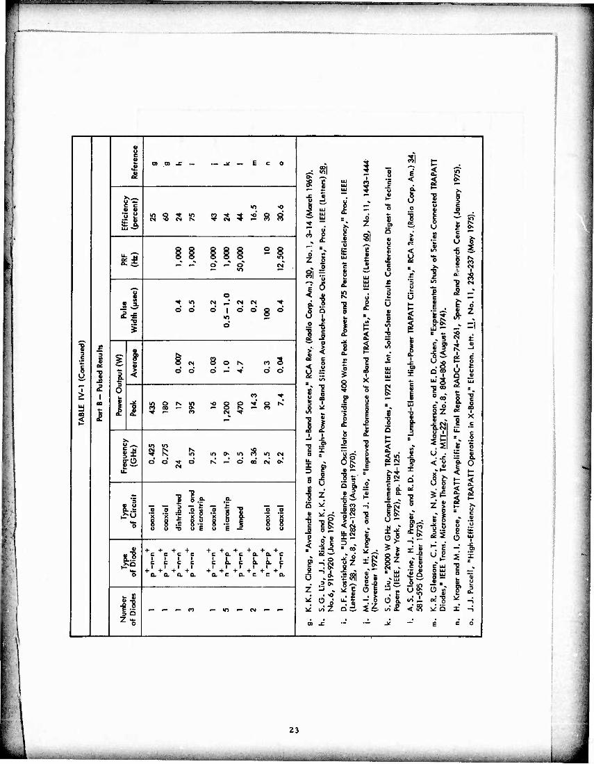
Table IV-2 indicates the output power, gain, bandwidth, efficiency, pulse width, and duty
cycle of representative state-of-the-art TRAPATT amplifiers. As above, the data are presented in chronological order, and the alphabetic reference scheme is preserved. All the
tabulated results are for pulsed operation. The bandwidth is given for a 1-dB-output power
variation.
. ■ ■ ■■ __^_. ^s^:,*.^ ± ;v.. v^.' ,f -t,^^ >.^%.;.

0 J3 u -D TJ <u u- «4- M. 14- <4\ S8 o 1 1
If? ^ u ml CN •o < K [
0£
\ 6 I
i
s CN
CN
0* z
SI
4- _c
UJ UJ UJ
z
s X
1 o
§ Q
1 c o
c
i'i C m J
<£ a ! n o 00
lO • O
o CN a ■* -o
•«*■ CM ro CN CN — u UJ
lO|
1 1 0
o 5 ü
"O i J3 u- l Ul
3 u 5 UJ w n
8 6 UJ UJ , > V»
1— a: < UJ X
.1 11 CO
•** CO 00 o
d ro d
lO CO ■*
rs -6 §
UJ m
o 0
0)
"8 5
c
1 x ,2 1-
u. o 0 s 1
1— (- 2 . 8
$ 6. | 0- v, q
UJ 1-
3 0 1-
0
1 oa
S5 P CN _o QS"
> UJ
< 1-
in CN CN o — CO
1- < a.
XO
£ i 1 Q- 1— .
Q S
-J 00
5 i <
1 3: d
IT)
d 00
d o
co"
00 (N •o 00
«^ CN s 1- «
| 5 | u O t- t-
u. u c
.2 "Ö
it UJ
i-
c 0
E o
. o .a 2 6-S
a^ 1"
T z
x > X QJ
c
t o
fl m a
. a. 1 ^_
< a. < a:
0
0
'x o 0 u
g 'x 8 u
o "x 8
g *x
8 o
'x o o u
o *x 8 o
.g "x 8 o
g 'x o 0 u
.2 .2 'x 'x 8 8 u u
I
00
_g VI 4)
|2
Qi.2
1-2
52 1
X o = z O) J
'5) ■*-
1 leg
" E
<
V + + + + + + + + + + ->' s _0) oi o-1 1.2 U 4-
«i c 1
c a. I
c 1
c a Q. 1
o. 1
Q. a i i *-i UJ CO <u d S • O
- S ^s c +
c 1
+ Q- 1
+ c 1
+ c 1
+ a i
+ a
+ a.
+ a a i i
+ + ■o 1 c a.
Q i\ S1"
«? 8 0 a a. c a a c c c c c if ||
> & u S • 'S
o
.? 1 O | 1 w rtj
_ _ _ _ ,_ ,_ ,_ ..... -_ p.. ^ o Q Z Z v>
. u.
t— 1/0
d "Z \ Ü s
Z •* ^ . , , „ 1 0 D JQ u ■o 0)
22
»aiiMa^faiaii*^^ ..,;.,.
SMHnoHpnnnnnDpHNnBHK
* I
c c «I «I
M *
II
8.§ £'0
0)
**- o
h Hi
I Q
o> at J: K - E
8 o •* m «O CM K 5 S 5 2 S R
2 8 — ^ o — o
in
^ Ml
d d
o CN „• <S CN ■* d | d d o d
d
Ö CM
d d n o o s
d d
IQ S CO CO rv in
CO £ 8
CM g 2 CO
in in
d m
o ■* —' d rt m CN
oo M o«
| l.o- .o. .2 .2 I .2 I .2 « "8 xxCxSxSo. 8 8 I 8-^ 8 -a §
ü E E -2
P .2 "x 'x 8 8 u u
+ + + + c c c c Mil +' + + +' a. a. a a
+ + + + + + c a. c a a c i i i i i i c a. c a Q. c
+ +' +' ♦' + +' a. c a c c a.
^^^C0 ^in — CN'- —
ooi -I ml
-g 3 I w < UJ
I u rt P
» «c
d j»" Z I
» J2 col •-
it 'S I
d J "8 o I
u
J
1 ? 11 » JS
"8 a u
-5 c
o
u I & c .S 'Ö £ c 8 £ IQ 1 o
S a.
I
il o g
= .2 -^
. .= Os Z ^ .
0 d u>Z
o z
SI 12
I
i i I-
"8
8 Z ? > I ö
.a
•51 "8^ a o> ^< o _ C CO 0 00
F ?d
III I
•Ü
> o &. E
c o U
3
Ö <l
s in
I
"3
■« o =• < in E <
U
1 > ai
Ci
<
iß "8 5
i I; c • « a
01
I a. i
o> I
c 4)
I I a. E 3
73 C o
Ü g -• §
Z
ez
o I
3 X
S ^ S ~ "8
T 01
- E 41 0) c u 11
in J. 2 6- in <E < S?
i g I o 0) c c o
U
o
c i E .
if LU ** B *.
* S £ ?
■§< U.S Q 00
■o 00
00 ^ • c o §z
o 3 C
I I J | ■5 ^ | ft
i s ^ CN
I ] «O CM
C O
CD
.2 u • -c < B
»i— x ^ o &•
U 5 . 01
£. >
V o II U S C UJ O UJ
8 £
— X
1 0
I I • i s i o 7
• -C — O)
■D C _- o —
\ \ 11 ._ _y —
I i
23

js-snigr?!,. - j ""■Mwr'TnrrTif-r'm'iiTr
i-.v
I >
CO <
Of <
<
I
HI
o ^ c c «I «I u Ji
lg «)
It
If
8.si
'S
0)
»I -g 8 I 5 2*8
«O O 8c<IO^ — ^ in ö o ■* iri o o o
S «o
CM CM O
o o —'
c s > "rö I
«N —
(N O
CN 8 Es
o I I O O O 0 6 Q io o m t t s — no n ö ■* 5 in
r>. io m co oö rs >o' co in o»
o o N io o IO
CM —
o o CO IT) S8 Ul o o
CM o^ in '— CM
K CN 2 8
CO CO O CO
^- ^ CO
CO CO CO
mic
rost
rip
mic
rost
rip
mic
rost
rip
o
1 mic
rost
rip
mic
rost
rip
mic
rost
rip
mic
rost
rip
mic
rost
rip
lum
ped
el<
+
+
p
-n-n
+
+
p -n
-n
+
+
n -n
-p-p
u-u
- d
+ + d
-d-
u + + d
-d-
u + + d
-d-
u + + d
-d-
u + + d
-d-
u + +
1= -
I \ S J I
CJ 0
• .E u c
_2 o > < u c V
> «I
0£
< u 0£
iß 3 •*- u 3 t
s o 5
s > "O CM 0) P. 1
.e Q. £ IS o- o.
tl X
<:l ■g i o S
< "5 A gü
Q.
a. E <
S ic ^
C o
CO
= a. J>
|S "i CO
o'l* o E s» 9 M
«I -i«" ü O>0£
,•1 z-t ^ 8
• u c
_o
<
o CO
I • t/1 ^^
. o«
1 0> «
I a> 5;
• u
If ° 2
| Si
, c X 3
X R 3 co
1 ^ co
O 0 7 ^ lOI i col
-—V
| i n f
V H- 0
X (J
o -c
« I a
l r c 5 S i
v3 i
8
c tl U
10
u o c s
^ i t < m tl
1 1
s - -8 i
3 •- -S •o CM
I Of t-
1
Bf Of
I U
I R CO
8 z o' Z
.v
O) tl
I r
E J
111 III ■ «T
•• —• ^ 0 ^ oo u k E o o Ü o -
-. |z S 6 .
^ CO . CN
3 00
o
I
s U * "5
c o u
o 8-
Of
2 3
o
I
r o «12
n * •-•
a Q. <
U o u
Ü
a> > o O
a. I
<s
J • II cZ
1-2 R u-
i >
13 o
11
24

T ■w^.n'iik^fii.^——...^..-'-^-..»«»-..—..■... :..-»:^,i..„^.^ -J""^^
CHAPTER V
AMPLIFIER DESIGN PRINCIPLES
; !
'!'
A. INTRODUCTION
The wideband TRAPATT amplifier is a two-terminal, large-signal, negative-resistance,
circulator-coupled amplifier. The negative resistance is induced by the application of an
external sinusoidal signal whose amplitude exceeds a critical value. The magnitude of the
negative resistance depends upon the TRAPATT semiconductor parameters, bias conditions,
and the external circuit. The amplifier behaves as a saturated amplifier, having a small
dynamic range, low gain and high DC-to-RF conversion efficiency. The microwave character-
istics of the TRAPATT amplifier have stimulated interest in its use as a final-stage amplifier
for a phased-array radar.
The operation of the basic TRAPATT oscillator, which depends upon the phenomenon of 17 "time-delayed-triggering," as described by Evans is reviewed in Sec. B. The reasons for
such circuits1 lack of suitability for broadband amplifiers are described and their design prin-
ciples are contrasted with the requirements for a true broadband amplifier. Section C presents 31 a theoretical procedure, based on Carroll's description of TRAPATT oscillators which
permits the design and synthesis of microwave circuits which will permit broadband TRAPATT
amplification. The circuit realization techniques developed for broadbanding TRAPATT ampli-
fiers are described in Sec.D. The unsolved problems associated with the operation of amplifiers,
including those which operate at harmonics of the fundamental frequency are discussed in Sec.E.
B. TRAPATT OSCILLATORS AND AMPLIFIERS
Time-Delayed-Trlggered Mode (Evans Circuit):- Realization of broadband TRAPATT
amplifiers requires special device and circuit characteristics which differ from those of con-
ventional TRAPATT oscillators and amplifiers. The majority of results reported for such
oscillators and amplifiers have been obtained with circuits which utilize time-delayed trig-
gering (TDT) as the oscillation-sustaining mechanism. A description has been published by 17 32 Evans et aL ' A fundamental characteristic of all TDT circuits is the requirement for a
low-pass or bandpass filter at an appropriate location between the semiconductor device and
the output load. A schematic diagram of the equivalent microwave circuit for a TDT TRAPATT amplifier is shown in Fig. V-l. The semiconductor device is connected to an output load resis-
tor through a network comprising the parasitic elements of the diode package, a low-pass filter,
and an impedance-matching network. The low-pass filter is located at an electrical distance 9 = (\ /2 - Ö), where 6 is small compared to A /2, from the TRAPATT device. The wave-
length \ corresponds to a frequency w defined as the normal-mode frequency for the TDT
circuit. An impedance-matching network, located between the low-pass filter and the output load, is used to adjust the circuit for optimum performance (either as an amplifier or oscillator).
The operation of a TDT circuit may be described with the help of Fig. V-l. If a sufficiently
large transient overvoltage is applied across the TRAPATT diode, a traveling avalanche shock
front (ASF) is initiated. During the time this zone travels across the depletion region, the
diode voltage drops and the diode current increases. When the ASF has completely traversed
the depletion width, the instantaneous diode voltage drops to nearly zero. Thus, a voltage step, whose magnitude is on the order of the diode breakdown voltage, is generated. This step then
25
iÜUttüttittiii ^^.^^M^M^m nnniiiiiii

jL't "•■''TTTiiimiiMBiiiiiiiiHiiiniiniriffii mi iiiiiiiuiiiiiiiiirTTrTT~r~~,,~',-n*'»TTTTTTtwrrim-¥riiiiiiiiiiiiiiiw^^^^^ mm
S = Xo/Z-8-
2V,
\
i—o—'mnp—f—o-'^fip—f—o
^cc
H -o-
=^Cr
(a)
hH-l«5«
LOW-PASS FILTER
IMPEDANCE- MATCHING NETWORK
si, < w, < 2iu.
- 1 is Z (T
u o
o > a o
TIME (b)
o TIME (C)
Fig. V-l. TDT TRAPATT oscillators: (a) simplified circuit model, (b) diode conduction current vs time, and (c) diode voltage vs time.
propagates through the parasitic reactances and along the section of uniform transmission line to the filter, whose high-frequency impedance is nearly a short circuit. The amplitude of the
reflected pulse is only slightly less than the amplitude of the incident pulse, but is, however, of opposite sign. The reflected pulse arrives back at the diode with a total time delay corre-
sponding to one period of the normal-mode frequency w . The diode voltage at that instant is
thus driven to approximately twice the diode breakdown voltage, a new ASF is triggered, and
the entire process repeats itself. Hence, the mechanism is self-sustaining. The strong de- pendence of the triggering mechanism on the circuit serves to emphasize the overall interde-
pendence of TRAPATT circuits and devices.
A TRAPATT oscillator is operated as an amplifier using an externally applied AC signal to initiate the ASF (Ref. 33). In the externally excited mode, each RF cycle must be triggered
only by the input signal. As might be expected, external excitation of the TRAPATT mode is
most easily observed when the frequency of the applied signal is close to w , the normal-mode
frequency of the TDT circuit. When the applied-signal frequency w is equal to the normal-
mode frequency w , the TDT enhances the triggering of an ASF. When w is different from u ,
multiple signal frequencies are observed at the output. In general, the two most important
frequencies are the applied-signal frequency w and the normal-mode frequency w , but differ-
ence frequencies can be observed as well. Observation of the normal-mode frequency as well
as the applied signal at the output port can be explained by the normal TDT mechanism. That
is, when the applied-signal voltage triggers an ASF, the diode voltage drops toward zero and
reverses rapidly. Thus, a narrow voltage pulse, whose magnitude is on the order of the breakdown voltage, is generated and propagates down the transmission line (as illustrated in
Fig. V-l). At distance 9 ~ ^r,/^. the pulse is reflected from the filter, as before, with near unity magnitude, but changed in sign. The reflected pulse then arrives back at the diode with
a total time delay of ZTT/CU = \0/c and instantly drives the voltage at the diode to about twice the diode breakdown voltage, triggering an ASF within the diode. This sequence is just the usual
TDT mode as described above, and the frequency of this overvoltage corresponds to the normal mode of TDT frequency a; . In general, TDT circuit amplifiers have relatively narrow useful
26
**^MiiftiMaitfi^^ n.„MM...... ^ .-..—.■■..■■ -;..i ...^— .__;

IWIWimillMIIMimil^1W^^^^Milll^ll«1M— ipillllll» 11 -mnmmmrn^^pnm^, ^:.^?,!m^. . ,.: . . ^_
34 bandwidths (on the order of 2 percent) due to this spurious signal generation, but may be oper-
ated in a Class C mode where large bias current flows only when an RF input signal is applied.'
Not all TRAPATT amplifier circuits mubt necessarily function in this TDT manner. The
diode terminal voltage generated in response to the impulsive diode conduction current incident
at terminal reference plane T can be adjusted to be self-consistent with TRAPATT theory
through the proper choice of the terminal load impedance Z(w). The TDT network described
by Evans is only one of many such circuits that is self-consistent with a theoretical TRAPATT
current and voltage waveform. The broadband operation of TRAPATT circuits will necessitate
the synthesis of such circuits which neither depend upon nor permit a narrowband triggering
mechanism.
C. CARROLL THEORY FOR TRAPATT AMPLIFIERS
1. Introduction
A simplified theory for the device-circuit interaction for Evans-type TRAPATT oscillators 31 35 was developed by Carroll and later extended by Carroll and Crede to include the effects of
the microwave circuit parameters on TRAPATT performance.
The Carroll theory is based upon the important insight that the interaction between a
TRAPATT diode and the associated microwave circuit in which the diode is embedded can be
approximated by a simple model. When the voltage across the depletion layer of a TRAPATT
diode and its time derivative exceed certain critical values, the device acts as an impulsive
particle current generator in shunt with the electronic reactance and the depletion layer
capacitance.
This basic model for the TRAPATT circuit and diode is shown in Fig. V-2. The diode is
represented by a particle current generator in shunt with the depletion layer capacitance C .
The quantities L , L , C , L , and C represent the electronic reactance, parasitic lead in- M a s* c r r r r
ductance, case capacitance, and a radial line transformation from the diode package to the TEM
mode in the circuit. An ideal low-pass filter is located a distance I from the diode package.
It is assumed that the low-pass filter passes the fundamental operating frequency unattenuated
and is a short circuit to all harmonics of the fundamental frequency.
The current generator H injects an impulsive current density that is induced by the charge
carriers generated by the avalanche multiplication. This is a particularly useful model because
the device physics of the ASF indicate that the induced current has a large impulsive compo-
nent which controls the voltage response of the circuit. The shape of the particle current H is
assumed to be that of a short pulse, as shown in Fig. V-2; whereas the total current through
the diode J is assumed to have a rectangular form that is consistent with Clorfeine's device Q
theory. These assumptions regarding J and H also determine the time-varying part of the
voltage V, since
H + C dV o dt k. J
Vdt (V-l)
It can be seen from Fig. V-2 that the voltage across the diode is self-consistent with the
TRAPATT mode theory (e.g., there is a large overvoltage that can trigger an ASF, causing
the diode voltage to drop to zero and then recover).
27
_= _:._ _..-. MSusämmm ----— immmmäitmimi^.... ,- lü

^^SB^^^^^SS^^SS!S^^^S!^tms:B!mmmmmmmmmmmmmmmmmmmmmmaKmmmmmKmmmmmmammmmmmu
fki^-ä HUhb
(b) n
(c)
tdl
t
hi-i-msil
■H(l) PARTICLE CURRENT
TOTAL CURRENT °
t/v
■■J
— T-J-^
tc S '-.■ *C, ^:C. Z,
(e)
LOW-PASS FILTER
Fig. V-2(a-e). TRAPATT diode voltage-current components.
The circuit used for the TRAPATT amplifier is different from that of the TRAPATT oscil-
lator in that the steady-state response of the amplifier circuit should exhibit a voltage waveform that does not have a sufficient "overvoltage" to trigger an ASF unless an external voltage at the
operating frequency is applied.
If we assume that the diode particle current H can be represented by a recurrent delta function with repetition period T, then
H(t) a Q RepT6(t) 0 < t « °o (V-2)
where I = Q/T is the average value of the particle current. The steady-state voltage across 8 the diode determined by Carroll making use of pseudotransients is given by
vo=vDC+voiHa^-v1cos,e-.) (V-3)
where V(e + ZTT) = V(e), e = wot u = 2ir/T, <p represents the phase of the power extraction
portion of the waveform voltage, and p («l/o) CZ 6) is a parameter which describes the time rate of change of voltage.
_^ ^_^ : ._ _;^_^
28
-^ ^___ ,:. ._..._.. „:

SSETöSSSS .r^ETBasBsurrH- rsa ^SMS ._ .r:i:;:--:5gs!F»M^
Fig. V-3. TRAPATT circuit voltage waveforms.
The elements of TRAPATT operation can be seen by examining this voltage waveform, as shown in Fig. V-3. As the diode fires (ASF excited), an impulse of particle current collapses
the reactive component of voltage from V to nearly zero, and it then grows exponentially as a
sinh function. The power extraction is modeled by adding an additional resistive voltage com-
ponent which is in antiphase with the current pulse, as shown schematically in Fig. V-3. The
maximum fundamental voltage swing is determined by the condition that premature avalanche
should not occur, i.e., the total voltage must not exceed V, prior to the reactive triggering of
the ASF. The reactive termination at the harmonic serves the function of pretriggering the
TRAPATT mode, while the resistive impedance that is added across the diode at the fundamental
extracts the power through the low-pass filter with a minimum alteration of the triggering pro-
cess. In order to trigger the ASF, the voltage must rise fast enough so that C 9V/8t exceeds
critical current at breakdown. This current, I rit. is given by I it = 'iNj-.v A, where q is the electronic charge, v is the high-field-saturated drift velocity, N^. is the ionized donor density,
and A is the cross-sectional area of the device. On this basis, if p is too small, the rate of
rise of voltage will fail to initiate an ASF. It should be noted that the charge Q must be suffi-
cient to make the circuit voltage fall to zero if the low-impedance plasma state of the diode is to be matched.
2. Admittance Characteristics for TRAPATT Amplifiers 35 From the Carroll analysis of Sec. C-l, we have shown that a self-consistent TRAPATT
voltage and current waveform can be represented by the sum of a DC voltage component, a
29
aaam.i,^^i«hai^=i,.i^,..feJ:&a

fr MMiMgp^a?^^
ÜN'
n \M-i-\iiii\
u ^«c ic' LOAD
Fig. V-4. Large-signal equivalent circuit for wideband TRAPATT amplifier.
reactive voltage component, and a power-extraction voltage component. Assuming that the
reactive voltage-triggering waveform can be generalized for all TRAPATTs, then an equivalent
harmonic driving point admittance, whose properties are such that the terminal voltage re-
sponse due to a periodic impulse current is self-consistent with the TRAPATT theory, can be
postulated. The circuit model used for determining the harmonic driving point admittance is
shown in Fig. V-4. The terminal current and voltage as a function of time were given by
Eqs.(V-l) and (V-3), respectively. The reactive voltage-triggering waveform, generalized
for all TRAPATT devices, is given by Eq. (V-4).
_ v sinhpQ - T) trig ~ o sinhpir (V-4)
where 0 < p < 1, 9 = w t, 0 < 9 < 2ir. The triggering waveform is reactive in that the power
dissipated per cycle is
Power ■H: trig H(t) dt = 0 (V-5)
The Fourier expansion of the reactive voltage is
CO
-4V. " V(t) 2 , 2 p + n
Re{exp[j(nwot-ir/2)l} (V-6)
The Fourier expansion for impulse current H(t) is given by
H(t) =i(t) =-2 ^- X Ree 0 .
The harmonic driving point admittance [ratio of I(nw ) to V(nw )] is
2 2 ^i \ v p + n
(V-7)
(V-8)
where Y = I /V , and I ■ Q/T. The Y(na! ) at the harmonic frequencies is thus specified for O O O O 0
the self-consistent TRAPATT triggering. 31 Carroll has shown that the low-pass filter circuit described by Evans will present an
admittance Y(na) ) which satisfies these harmonic admittance requirements over at least a
decade in frequency. However, the time-delay triggering associated with the Evans-type cir-
cuit has limited such amplifiers to narrow bandwidths.
30
- - L_ L •_ „.-•._ _ . ... ._.__

■T.... ..„. „^.m u Wpl|.pW^w..yfp^!wWa!|pTiWwW.il)P t ...y.i.iiu.mm9mmwmmm^^mm^mmsmmmm^^!mrw^^-i ■--'■. ->
D. WIDEBAND AMPLIFIER CIRCUITS
1. General Circuit Conditions
Investigations of TDT amplifiers and oscillators have defined certain circuit and device
parameters necessary for achieving broadband TRAPATT amplification. The circuit model de-
veloped for broadband amplification is shown in Fig. V-4. The TRAPATT device is represented
by a parallel circuit comprising a conductance G^j, an electronic susceptance BD (which repre-
sents the active portion of the diode), and a capacitance C representing the depletion layer
capacitance at breakdown. The inductance L and capacitance C represent parasitic lead in-
ductance and standoff or package capacitance. The inductance L and capacitance C represent
discontinuity reactances due to the connection of the diode mount to the microwave circuit.
The filter network defined at reference terminal planes T?-T, forms the microwave
impedance-matching network that performs the necessary fundamental and harmonic imped-
ance matching for the TRAPATT device.
The terminal voltage-current characteristics and bandpass performance of the TRAPATT
amplifiers can be predicted from the input admittance Y(u) at terminal reference plane T. and
the transfer characteristics H(w) of the impedance-matching network formed by the network
elements between terminal reference planes T. and T-.
The power gain of the amplifier is given by the square of the magnitude of the reflection
coefficient |r| at reference plane T., i.e.,
Power Gain Y(w) +GD(w)l (V-9)
where GD is the large signal conductance of the TRAPATT device and is negative at the funda-
mental and harmonic frequencies. Broadband efficient amplification is obtained when the microwave impedance-matching
filter fulfills the following conditions: 33 (a) Grace has identified five device-circuit interaction conditions:
(1) Im Y(w0) » 0
(2) Re Y(a)o) = -KG
(3) Re Y(nwo)
(4) Re Y(nw0) > 0
(5) H(na) ) = f1' n = *
D
n > 1
L0, n > l)
Network is resonant at the output frequency.
The factor K is chosen for the desired gain.
To minimize real power dissipa- tion at harmonics of « . o
To allow for the fact that some harmonic power is both generated and dissipated.
A single frequency output is de- sired, where H(nw0) is the power transfer function of the network between the terminal reference planes Ti and T3.
(b) Carroll's theory, supported by experimental measurements on trigger-
ing waveforms shows that for good TRAPATT operation Im Y(na) ) must
be positive and increase monotonically. A plot of Im Y(nw ), calculated
as described above, vs harmonic frequency is shown in Fig. V-5.
31
MMiaiifa mjäMii äü^ÜMu ^^Lc^^^^äMlMiMMt^

mwinmmnw^-mwvv.. ^'^^'"I'^yy^^'-^igj^yiiajgjlg! .•■....,,«.,,.,-,. ... . .aasaKÜfel
33 (c) Good TRAP ATT performance is obtained experimentally and in
computer simulations when a small circuit susceptance is presented
in the vicinity of the 2nd harmonic, 2f . This small susceptance demands that a high 2nd-harmonic voltage be developed if current
flows at 2f . Such a current will be present, since the active diode is a nonlinear element and will develop a 2nd-harmonic current
from the input (signal) frequency. High voltages at the 2nd har-
monic aid the development of the large voltage swings which are
required to trigger the ASF, especially if the TDT mechanism is
not present.
(d) The slope reactances (dX/dw) at all frequencies should be minimized,
i.e., the tuning elements should be located as close as possible to the
diode terminals.
o x
e 3 e Fig. V-5. Harmonic reactance
behavior of wideband TRAPATT amplifier.
Two types of TRAPATT amplifier circuits have been developed at various industrial labo- ratories that exhibit wideband TRAPATT amplification. The first wideband circuit, originally
developed at RCA and used by both Sperry and Hughes, utilizes a distributed coupled-line
microwave circuit as the filter network. A recent wideband circuit developed by Sperry uses
a circuit comprised essentially of lumped circuit elements. Both typical amplifier circuits
are capable of 5 percent or better bandwidth performance with a variety of different types of
TRAPATT devices.
To be useful, amplifiers must simultaneously exhibit high power, high efficiency, and
broad bandwidth. Like many other microwave solid-state devices, TRAPATT diodes develop high power at low impedance levels, where the circuit impedance matching is difficult. Fur-
thermore, the TRAPATT device is a multiple-frequency device and must be properly ter-
minated at its harmonic frequencies for stable, efficient operation. Finally, the requirement
for broadband amplification makes the TRAPATT amplifier circuit design task even more diffi-
cult, since proper termination must be provided not only at a set of frequencies, but over a set of frequency bands.
2. Coupled-Line Amplifier Circuit
A coupled-line microwave circuit is useful for wideband TRAPATT amplifiers, for such
a line can provide an extremely wideband impedance transformation, even harmonic filtering.
32
,..„,:.., ^.^,,„.. _-„ „ ., . äMääii^ß.^**^^.^,^.^^

1 '•" ''^': ' :: ''• •v "niPwiiiiwiiiiiiiiMiiiwniiwiiMwwwMwwiwwiiiiniwi
|U-i-H5>l|
PORT 1
'1 z... z.
Fig.V-6. Coupled-microstrip trans- former: (a) four-port coupled-line circuit and (b) side view of coupled- microstrip circuit.
PORT 2
M (a)
i. W H. S,|, W .i -MICROSTRIP
_i IfVVWl BBSB -DIELECTRIC SUBSTRATE
^ GROUND METALLIZATION
(b)
and an additional advantage of DC isolation due to the air gap between the lines. The basic
structure of a coupled-line transformer is shown in Fig. V-6.
The theory of the coupled-line circuit has been shown by Collard, and the equations are
repeated here for completeness.
Zll Z12 Z13 Z14
Z21 Z22 Z23 Z24
Z31 Z32 Z33 Z34
Z4t Z42 Z43 Z44
111 h\
i x h\
>'
(V-10)
where
Zll = Z22 = Z33 = Z44
Z + Z . oe oo 1
Z12 = Z21 = Z34 * Z43
Z -Z , oe oo 1
z -z oe oo Jl-S* 2 s
Z + Z oe oo 7i-s2
Z13 " Z31 = Z24 " Z42
Z14 = Z41 = Z23 ': Z32
Z = even-mode impedance of the coupled line
Z ■ odd-mode impedance of the coupled line
S = j tan e
9 = electrical length of the line.
33
Mjaiaa^g^.^..,^.,.^..^^^

' r mmm?,^.^*—^
ZL < PORT I
|ll-i-1936Zl
A11-A12 A22-A12
A12 1 T2 4 PORT 2 ■¥ DIODE Fig. V-7. Two-port equivalent
of coupled-microstrip circuit.
tl-3-19JtJ
4 3
C i
ZM
WHERE Z >
Y =
2Z„, N= 1 +
Fig. V-8. Coupled-line circuit and transformation.
34
.. ^^^ haaMiaMMiiliaa^MBa^^^
1-. - _'-_ "'j - - .' . . ■ "• , ... iTMCTISB
When ports 3 and 4 are terminated with impedances Z, and Z., it is possible to represent
the circuit of Fig. V-6 in terms of a two-port network as shown in Fig. V-7. The elements of
the equivalent circuit are defined as follows:
2 2 AH = Zll " (Z4 X Z13 + Z3 * Z14 + Z14 ^/^^S2 A')/A
\Z
21
Z,, -(2. xz,- XZ„ + Z, XZ,. XZ., +Z,, «/I -S" AM/A "12 13 J32 "14 "42 J13 <Ji -;
Z21 " (Z4 X Z31 >< Z23 + Z3 >< Z4i x Z24 + Z24 Ji - S2 A' )/A
A22 = Z22 " (Z4 X Z23 X Z32 + Zi x Z24 X Z42 + Z23 7l -S2 AM/A
*,.•<
A'=Z33XZ44-Z34XZ43
A = (ZJJ + Z3) (Z44 + Z4) Z34 >< Z43 (V-ll)
In terms of these parameters, the impedance of the network at the device terminals can be
calculated as:
Zin = A22 A 12
11+ZL (V-12)
r' 1 ?
A useful coupled-line circuit configuration having an open-circuited termination at port 4,
a short circuit at port 3, and the input and output at ports 1 and 2, respectively, and its equiv-
alent circuit is shown in Fig.V-8. The equivalent circuit of the coupled-line network can be represented as the series connec-
tion of a shunt stub, ideal transformer, and series stub. If the length of the stub is chosen to
be X/4 at the output frequency, then the coupled-line network behaves as a wideband transformer
at the output frequency f . The transformer may be either "step up" or "step down," depending on which ports are chosen as input or output. The coupled-line network exhibits stopbands at
the even harmonics and passbands at the odd harmonics. For the TRAPATT amplifier applica- tion, the TRAPATT device is connected to port 2 and the transformer is operated in the "step
down" mode.
There are multiple choices of even and odd mode impedances for any specified impedance
transformation ratio. A typical 10 to 1 impedance transformation with two sets of even and odd
mode impedances is calculated and plotted in Fig. V-9. It is obvious that the wide-line coupled-
line circuit provides a flatter frequency response for the reactive loading than the narrow-line
circuit of the same transformation ratio. Broadband TRAPATT amplifiers require relatively
flat frequency response at the output frequency.
Computer calculations of the depletion-layer voltage for an F-band coupled-line amplifier
shown in Fig. V-10 were made at Sperry Research Center, and the waveform is shown in
Fig. V-ll. The calculations show that the depletion-layer voltage response to periodic impulses
of current is self-consistent with the TRAPATT theory. That is, there is only one avalanche
event per cycle and the product of C and dV/dt preceding the voltage maximum exceeds the
critical current density.
; m
_^ _^
35
ÜÄÜÜfc^ I ■^^■^-- ..-.^aw^^

_ _ JT ■ ■ '°MMI1lllWWWiffMWlWWTWWyP,™™™s™l™™"™i^^ '
«0
-
i i i 1 1 T" T | II
60
Lit I-W3M w
40
20
- I* •50 ohm« ' /
/ s
-20
-
/ /
-40
-60
- /
/ /
/ CIRCUIT 1: Z, = 42 S/H=0.1 .
/ Z,= 22 W/H» «T
CIRCUIT 2: Zt= 89.5 S/H = 0.2 Z,,» 46.9 W/H» 1.8
-■0 I I 1 1 1 1 J .J 1 1 1
•i
0 1.2 1.6 2.0 2.4 2.8 3.2 3.« 4.0 4.4 4.» S.2 3.6 6.0
FREQUENCY (GHi)
Fig. V-9. Impedance behavior of coupled-line transformers.
BIAS INPUT 11-3-H385|
RF BYPASS CAPACITOR AT TOP AND BOTTOM PLATES
INPUT-OUTPUT CONNECTOR
TO CIRCULATOR t(rod)
Fig. V-10. Coupled-line amplifier. Fig. V-ll. Calculated terminal voltage for coupled-line TRAPATT amplifier from Carroll model.
36
.,.f,....^a.^aa.aa^^^^ . ...... ., i^tiBiirtiiiiitoMiiii^ ..^....i....,,..^.^..^.^..^,^^

" ■■■.■..■^'■■;■ '■'■■_ _'' "ll ■"mi""'" ^fiiffifiiii|m fpf|1ffflru^(BIM|»»irTnill iiiir^TfBirinBiM""fflmfflii .Bnnwi»««"«"
!
I
3. Lumped-Element Circuits
Broader bandwidths and higher peak power should be attainable if a less frequency-
sensitive impedance-matching network were used in place of the coupled-line filter and, in
fact, a lumped-element network is capable of satisfying these requirements at F-band with
reduced frequency sensitivity. A lumped-element impedance-matching network was developed
from the amplifier design principles described in Sec. C. The generic form of this circuit was
synthesized using a computer simulation program at Sperry Research Center which calculated
the gain and terminal I-V characteristic.
A simulation of the diode I-V terminal characteristic is shown in Figs. V-12 and -13. The
periodic impulsive current was assumed to have a wave shape H(t), as shown in Fig. V-12,
which was modeled after current wave shapes observed from a UHF TRAPATT amplifier using sampling techniques. This driving current formed the input to the computer simula-
tion, and the resulting voltage waveform was found to be self-consistent with the TRAPATT theory.
i
i
Fig. V-12. Assumed impulse current waveform.
Fig. V-13. Simulation of terminal voltage waveform for 50-W wide- band lumped-element amplifier.
The final circuit components were optimized with the aid of the design principles described above. Under the constraints that the device is resistively terminated at the fundamental fre-
quency to achieve the desired gain and reactively terminated at the harmonics, the circuit parameters were systematically varied in computer experiments. That combination of circuit
components which yielded the maximum overvoltage with only one avalanche even per cycle was chosen for circuit fabrication.
The amplifier circuit was optimized for maximum gain bandwidth for large area devices
which were capable of peak power performance at either 50- or 12 5-W levels per device. The
large area diodes present most difficulty in obtaining broadband amplification, since their
large-signal negative resistance is quite low (—R & l/area), and requires a greater imped-
ance transformation, while their large junction capacitance presents higher reactance slopes.
A schematic diagram of the resulting optimized lumped-element amplifier is shown in
37
- ^j tori&Mtfsa»aiMiMa^^ mm^mM^f^uiäji^M^^jt^iii^üi^iä i :.. ^^i::^..J

m~, '*^,l^^^^^w,w^^^W^wiwWp™-^w-™^--w-- ■PPPÜP
PARASITIC MOUNTmG REACTANCES j U-i:19lin
^T0 ACTIVE PORTION
OF TRAPATT DEVICE
PARAMETERS FOR 125-W AMPLIFIER
C, =4.0pF C, s 2.2 pF VB= 80 V
L|=0.58iiH L4=0.30nH I0C-6A
C, = 0.249 pF C, = 0.30 pF
L2 s 0.084 nH Z, ■ 50 ohms
C2 =0.045 pF 9, = 0.86 in,
L= 0.254 nH C =1.4pF
Fig. V-14. Schematic diagram of lumped-element 125-W TRAPATT amplifier.
Fig. V-i5. Photograph of 50-W amplifier.
Fig. V-14, with appropriate parameters for the 125-W case. The active portion of the
TRAPATT diode is represented by a periodic impulse generator H(t), an electronic suscept-
ance BF, and the depletion-layer capacitance C The parasitic reactances associated with the
semiconductor chip mounting and connection to the external circuit are represented by the
inductances L., L,, and L^ and capacitances C. and C?. Capacitors C. and C- and the shunt resonator {L. — C.,) form the impedance-matching network for the amplifier. Capacitors C,,
C., and C, are variable capacitors used to tune the amplifier for optimum performance. The
values of the parasitic mounting reactance were dictated by the type of diode mounting and the microwave transmission line used for the amplifier.
38
^..-.-.C-- .-r. ■:-.:■■'.■. ■■■.■:■■ .. .V.- ,.■.■:...V.-....,- ^t^m&itä&^.^X***^^

lEIESSS IIIIMWIimilimWUHWMHIIlllllMllllll ■■■m p»)j-iTTfTTTT|wm.T1||||w|||1|||)|||||||||||||||||][ zsS.:l^Uia
The 50-W amplifier was designed for microstrip using l/16-in.-thick Tellite substrates.
The devices were mounted in a varactor package and threaded into substrates, as shown in the
photograph of Fig. V-15. Table V-l shows values computed for the 50-W amplifier parameters.
Note that for this case, capacitor C' was not required. Single-tuning capacitor C^ (Johansen
Model 72 83) is mounted adjacent to the diode and connected via a high inductance to the 50-ohm
lines. The capacitor C, is tuned from the back of the circuit by a screwdriver adjustment. The 50-ohm line extended over the diode to provide some capacitive (this is represented by
variable capacitor (.' ) tuning for the amplifier.
TABLE V-l
i 50-W TRAPATT AMPLIFIER PARAMETERS |
C. =2.5pF 1
L3 = 0.298 nH Z = 50 ohms
L^O.SSnH C3 = 2.31pF V0
<:, = 0.249 pF L4 = 0,30nH VB=87V
L2 = 0.138nH C4 = 0.3pF 'DC-^
C2 = 0.045pF c5 = o
The computer simulation for the TRAPATT terminal J-V characteristic made use of the
calculated harmonic admittance measured at terminal reference plant T . A plot of the ad
mittance for the first seven harmonics is shown in Fig. V-l 6; also shown is a plot of the
0.4
0.3 -
Fig. V-l 6. Driving point impedance for first nine harmonics for lumped- JT element amplifier.
I 0-2
o.i -
T |ll-3-)»T0]
O -
O SIMULATION
• THEORETICAL
J I L 12 3 4 5 6 7
HARMONIC NUMBER
39
- ---- ^ feiiMMii^^ ^ |ir ^^aa^aa^

^^^SriL " -iSC"—ZZ-LTZIT- _ „ - •::%"" ■■:--.V'-:;;;v"':;^/:•: r^;:~-v:-r>-i :^-.^
theoretical harmonic admittance calculated using Eq. (V-8). The value of Y = 0.0355 and the
value of p, defined following Eq. (V-3), was assumed to be 0.75, which is consistent with the 35 theoretical calculations of Carroll. Good agreement between experimental and theoretical
calculations helps to increase the confidence in the use of the Carroll model for the design of
TRAPATT circuits.
E. HARMONIC EFFECTS
Most TRAPATT amplifiers and oscillators operate using the fundamental extraction mode; i.e., the output frequency is at the same frequency as the ASF frequency. However, it is
possible to obtain energy at harmonics of the ASF frequency due to the large-signal-harmonic 37 negative resistance of the TRAPATT. The harmonic content of the voltage and current wave-
form is sufficient to extract relatively high harmonic powers. However, the efficiency of
power generation will be lower for harmonic extraction than for fundamental extraction.
Fig. V-17. Computer simulation of the terminal voltage and current for a 2nd-harmonic extrac- tion amplifier.
The reduced efficiency for harmonic extraction may be seen conceptually from voltage
and current components necessary for maintaining waveforms which are self-consistent with
TRAPATT theory. This is illustrated in Fig. V-17, which shows the computer-simulated ter-
minal voltage and current for a 2nd-harmonic extraction F-band amplifier. The ASF frequency
is 1.6 GHz and the 2nd-harmonic output frequency is 3.2 GHz. The amplitude of the 2nd-
harmonic voltage is 27.9 V and the fundamental voltage amplitude is 28.6 V. The shaded area of Fig. V-17 represents power dissipation because the RF voltage is positive and the terminal current is high. The efficiency for harmonic extraction can be shown to be lower analytically
than for fundamental extraction in the following manner.
40
- ■ ■ - ■ ..■ - ^- ..■..'-.....;.-' l. : : ^ ...,;.. '..-..,....■■.■:^.^1^.^.., _..._ :... _._. _....._... __ _ _._.__ J____ .,JJM,,aa»a
'iimmTiM^^ww?M!ls^F!^'tsmmr^m«is^m^'m , .. ■., ,, "'.., i. . .'- _j^^
The peak-to-peak amplitude of the voltage of the extracted signal is limited to the break-
down voltage to prevent multiple impact-ionization processes per cycle. The power generated
by the TRAP ATT is therefore limited to
VBl(nw ) P(nwo) < 2 [cos(p(nwo) + TT]
where I(nw ) is the harmonic amplitude and (p(nu ) is the harmonic phase. P(nw ) is negative
for -7r/2 < (p < v/Z indicating power generation. The Fourier coefficent I(na) ) of the 2nd
harmonic of the impulse current will always be less than that of the fundamental* Knw ) < I(« ).
Therefore, for a given breakdown voltage, the 2nd-harmonic power generated will always be
less than the maximum available at the fundamental. In the computer simulation shown in
Fig.V-17, the fundamental extraction efficiency was 27 percent, whereas the 2nd-harmonic
extraction efficiency was 12 percent.
<'For an impulsive type waveform with nonzero width, the Fourier coefficient, amplitudes decrease as n"a, where 0< a< 2.
:.^.^„. :■■■■■■ ■ _^ ^.-....v,:;. ^ ._, ^ . ■ . ^ ,,, ... ..

^fWT--***?*. !!«WRiliP«P»P!*!.WJ
CHAPTER VI
EXPERIMENTAL RESULTS
A. INTRODUCTION
TRAPATT amplifiers have been constructed in several distributed circuit media forms, in
some cases including lumped elements as well. The degree of design sophistication has varied
from pure cut-and-try techniques, using either coaxial slugs or plated ceramic chips as movable
tuning elements, to exploitation of the theoretical concepts discussed in Chap. V. Some of the
more significant results which have been reported are discussed in this chapter, and results of
measurements made at Lincoln Laboratory also are described. These provide representative properties which are characteristic of the best amplifiers
achieved to date, and may be taken as benchmarks of the current state of the art.
B. COUPLED-LINE AMPLIFIERS
Coupled-line pulsed TRAPATT amplifiers have been investigated at RCA, Sperry, and Hughes. These circuits have been developed using both microstrip and slab-line geometry.
The best results at RCA were obtained from a coupled-line microstrip circuit including an
external idler resonator circuit as illustrated by the photograph shown in Fig. VI-1. This net-
work, when provided with a tunable external idler, yielded some capability for broadband 2nd-
harmonic amplification in F-band.
DC INPUT
LUMPED C iPACITOR
COUPLED-LINE CIRCUIT
IDLER CIRCUIT
Fig. VI-1. TRAPATT amplifier with hybrid idler circuit.
The basic amplifier consists of a microstrip coupled line and hybrid idler circuit connected
in series with a lumped-variable capacitor to ground. The resonant frequency of the idler cir-
cuit was tunable from 1.3 to 3.8 GHz, by means of capacitance adjustment. The coupled-line
impedance-matching transformer matched the diode impedance to the 50-ohm load at the output
frequency. A photograph of a broadbanded version of this circuit is shown in Fig. VI-2. In order
to reduce the parasitic effects associated with a packaged device, an unpackaged TRAPATT di-
ode was mounted in chip form. The diode was mounted at the end of a gold-plated brass stud
by means of a conductive silicon heat sink compound, and the stud was then inserted into the
circuit from the back of the supporting block to insure good electrical contact with the back of
the microstrip line.
*— ■ --■-- ir
43
mS^^!Ui^,m^umt,MUm..u^^.^.i. >.t-,^,JJ.^mJ^^a^..taM^J|B
|aape^~'rjtpp**«£ä^*,f-..':
liflSCEDIIG PA3Ä4'|UNK-N0T FILMED,
•^^•^•^ ^^a^jU^.^^.a...

PjWJIBWi'' " ' ' '■" " y ■ " "■ - "—»2w«^2^'T?^r'""'"','",',:_fcÄ««»'
DC INPUT
COUPLEO-LINE CIRCUIT
IDLER CIRCUIT
Fig. VI-2. Broadband coupled-line amplifier.
v<
TABLE V -1
SUMMARY OF I RESULTS38
Power Output (W)
Single Diode
KR9D No. 5
Single Diode
KR9D No. 2
Two-Diode Stack KR9D
82 83 166
Bandwidth (percent) 9 (IdB)
narrow 3.09 to 3.14 (3 dB)
Gain (dB) 4.9 6.3 7.55
Pulse Width (Hsec) 10 50 10 i
Efficiency (percent) 15 10.5 10.15 |
,
100 1 1 1 1 1 1 1
^^- >r^^N^J
a. t-
O
80
60
•^ 1 a bj 40
CRUCIFORM DIODE I
20 _ KR9D No.5 DOUBLE DIFFUSED
PULSE WIDTH: IO/IMC j
0 I I I II II
5
4 a
« f o
1
o Fig.VI-3. RCA S-band TRAP ATT amplifier properties.
3.0 3.1 3.2 3.3 3.4
FREQUENCY (8Hj)
3.S
44
:.. ^ ..i..^...: :.....;■,-.../■.::..» ,.^^,.»ji!>...^.J,!,„..;:.:,,'a...J.;.. j...^..^ ......,J...a.....i, iaaaHfe^^^&^^.iiiiMi^^

'' I 'I I [UM^^^^^^^^™^^^^^^nmMwmmMmmmm^mmm*~mm**m*mm.*.^mmn..lr™*m^-rnmlymr rm—n J-—-»
Ized in Table VI-1. The best results reported for the coupled-line idler circuit are summarized in Table VI-l.
Wideband amplification was obtained over the 3.25- to 3.55-GHz frequency band (as illustrated
by the passband shown in Fig. VI-3). A maximum pulsed output power of 82 W, with a peak mid-
band gain of 4.9 dB was obtained using a pulse width of 10 |isec. The best power-added amplifier efficiency of 14.7 percent was obtained using a current pro-
filed across the frequency of operation. At 3.25 GHz, the current was 4.5 A and was increased
to 6.5 A at 3.55 GHz. In addition, RCA has achieved a maximum output of 166 W using a two- diode series stack with a maximum gain of 7.55 dB. Power-added efficiency was 10.15 percent
with a 10-(isec pulse width (see Fig. VI-4).
a
180
3 izo o
* 100
80
60
-JJ-T-n- I ' I
7 y r\ \y
s s
', I ' .I |ll-3-H3IO|
J L_L
MAXIMUM GAIN 7.S5dB
MAXIMUM EFFICIENCY 10.16 PERCENT
PULSE WIDTH lO^istc
I I I I I I I I I I I I -Jf- 0 3.10 3.12 3.14 3.16 3.18 3.20 3.22 3.24
FREQUENCY (8Hl)
Fig. VI-4. RCA two-diode power frequency characteristics.
80
- 60
O 40
20 -
460 MHJ
3.0 3.1 3.2 3.3 3.4 3.5 3.6
FREQUENCY (GHz)
Fig. VI-5. Performance of double-diffused- mesa TRAPATT amplifiers.
RCA also has observed up to 195 W from a single diode at a power-added efficiency of
20 percent and maximum gain of 6,27 dB across a narrow bandwidth.
Double-diffused-mesa diodes were reported to provide amplification with 300-MHz 1-dB bandwidth centered at 3.3 GHz. The peak output power was 70 W at 18-percent efficiency, and
midband gain was 4.1 dB, as shown in Fig. VI-5. Similar power levels, bandwidths, and effi-
ciencies have been achieved using variations of the coupled-line circuit at both Sperry Research
Center and Hughes' Torrance Research Center. The Sperry Research Center also has investigated a slab-line geometry coupled-line am-
plifier circuit. In this circuit, the TRAPATT device is mounted in a varactor package located at the output port of the coupled-line network, as shown in Fig. VI-6, The parasitic lead induc-
tance of the TRAPATT package was chosen to optimize the amplifier performance.
Under low-power pulsed operation, a — 1-dB bandwidth of 300 MHz was obtained with a nom-
inal gain of 6 dB, as illustrated in Fig. VI-7 (Ref. 24). The power-added efficiency of the am-
plifier was reported to be 20 percent at midband. Computer calculations showed good agreement with the measured passband. The broad bandwidth was attributed to the diode being resonated
at the output frequency by the parasitic diode mounting reactance. This eliminates the long-
lines effect of tuning on the output of the coupled-line network.
^^ _.__._ üüHIü -
45
imäMimbimiamämäiämaälitMiätäliS&t^ a;^:^.i..i...:.,-J.,..,V..V,:i..,./^^-.t.J

;:>^-:;:'^^^"—^'^-T^V' v^T^^
1B-M8365|
RF BYPASS CAPACITOR ,, ,,., , „, AT TOP AND O' TRAPATI OtViCE
BOTTOM PLATES
INPUT-OUTPUT CONNECTOR
TO CIRCULATOR
Fig. VI-6. Coupled-line amplifier.
7,6 1 1 - 1 II I 1 [J| 5 li'iftl
6.0 - r^\~ >v —
»4.6 _ / 1 _
g o '■o
OUTPUT. rs \ .
\ AV / INPUT / \
1.6 ^S X \
S p^ —C— ^^-^
0 1 1 1 1 1 1 1 2,6 2.9 3.0 3.1 3,2 3.3 3.4
FREQUENCY (GHz)
Fig. VI-7. Measured passband for coupled-line TRAPATT amplifiers.
Fig. VI-8. Typical input-output power characteristics of TRAPATT amplifiers.
RF INPUT POWER (*)
Li ^ ^^^m^i^maäiM^M^
46
. . :■ ■ ■ ■.. , L^ _^ ■ .A-:.: ,-

JJ(!I3™'^I5»'J!K$S'WW[JFF"5 ■■■■■" ■ ■; ■ ■ ■.'.'■
TRAPATT amplifiers are large-signal amplifiers and do not exhibit net gain until the input
signal amplitude exceeds a critical threshold value. For signal levels below the critical thresh-
old value, the TRAPATT diode presents a relatively good impedance match to the circulator,
and the amplifier exhibits a loss. When the input signal level exceeds a critical threshold, net
gain is observed. There is a small dynamic range where the amplifier is linear (3 to 5 dB).
At higher input power levels, the amplifier saturates, and the output power remains constant and then decreases. This is illustrated in Fig. VI~8 which shows the input-output power char-
acteristics measured for a typical low-power S-band coupled-line amplifier.
C. EXPERIMENTAL LARGE AREA DIODE AMPLIFIERS USING LUMPED-ELEMENT CIRCUITS
Wideband amplification has been obtained at both the 50- and 100-W power levels using a lumped-element microstrip circuit developed at the Sperry Research Center from the amplifier
design principles described in Chap. V. A photograph of the lumped-element amplifier is shown
inFig. VI-9.
Fig. VI-9. Lumped-element 50-W TRAPATT amplifier.
The 50-W amplifier was a microstrip circuit design on Tellite substrate including lumped
elements as described in Sec. D. Diode capacitance at breakdown was approximately 2.5 pF, and
a -1-dB bandwidth of about 300 MHz was obtained for a nominal midband gain of 6 dB. Sperry's
reported results are illustrated in Fig. VI-10. The peak output power was 50 to 60 W for a
l-nsec pulse width at a 0.001-percent duty factor. The measured passband agreed well with the calculated passband, assuming that the diodes
may be represented as a frequency-independent negative resistor over the frequency range of
interest. The broad bandwidth is attributed to the fact that all tuning is accomplished with lumped
elements in the vicinity of the device, thus reducing the long-line effect of distributed circuits.
Long pulse operation with the lumped-element amplifier has been obtained using 2.5-pF ca-
pacitance diodes of a ring geometry mounted on diamond heat spreaders. Peak pulsed powers
47
^iz^..,,uÄ^AL^^x*^i^i±^^ ii^^^i^Av^fe.Vrttf,fe^^^ . ■,.. | ■ .|i|.

p*r ww» w"1-■-«»■<•■*«] 'u,»I ii.^imi™,! u.ai«a<«< ■!■ ui.."-^- ™. ii . i i muiiin »nn I..I«I^ ■n^:v,:-..^v^-.£j~'.y-;-'vr™ 5.'w^Ej3Eläi^:.,:
70
60 _ 1 I 1 1 1
|ll-3-l93t4|
^ to -
, S \^ Pio • 9 TO 10*" 40 _ S ^"^K
ÜJ
8 JO -
f C^S.ApF VB = 62V
20 - I =2.8 A EFFICIENCY « 21 PERCENT
10
0
— 1 1 1 1 1
2.9 3.0 3.1 3.2 3.3
FREQUENCY (GHi)
3.4 3.9 WO-U37
Fig. VI-10. Passband of Sperry 50-W amplifier.
Fig. VI-11. Lumped-element 125-W amplifier.
§ 80
B u i £ 60
ia-3-it3as
Cj = 3.85pF AT VB
■t- f23- 117-
PERCENT MAXIMUM PERCENT MINIMUM
INPUT POWER
3.0 3.1 3,2 3.3
FREQUENCY (GHj)
Fig. VI-12. Passband of Sperry 125-W amplifier.
48
.. ■ .... ., . ...' -. ... . .... ..,.......a...1.-;^ii;.jia.J.,Ji...., J,«j,t^.ti..iJ.-a^.~^^».-».

■"■.' ,■■ . ,:/I .,^._ - ,, . .. - .'. ■ .
at the 30- to 40-W level have been measured using 50-(isec pulses at a 0.001 duty factor. Higher
duty factors were not attempted; no forced cooling was used. The midband gain was 5 dB, and the efficiency was ~20 percent.
Peak output powers of ~125 W have been obtained using larger area diodes (4.0-pF capaci-
tance at breakdown). The lumped-element circuit was modified to include a third tuning capac-
itor Cy A photograph of this amplifier is shown in Fig. VI-11. This tuning capacitor is located approximately a quarter wavelength away from the TRAPATT device and serves as an impedance-
matching function to help present the required circuit impedance to the reduced negative resis- tance of the larger area devices.
The larger area devices were reported to be capable of saturated peak output powers of 100 to 125 W at a midband gain of 5 dB and a - 1-dB bandwidth of 200 MHz. The midband power-
added efficiency was approximately 23 percent. The passband of a typical amplifier using in-
verted complementary devices (n -p-p ) is shown in Fig. VI-12. The reduced bandwidth is attri-
buted to the difficulty in matching the load to the reduced value of the large-signal negative
resistance associated with the larger area devices.
Amplifier results were obtained using inverted complementary (n -p-p ) type devices rather
than the conventional p -n-n devices. The —1-dB bandwidth was generally 20 percent greater
with the n -p-p devices.
D. DEPENDENCE ON OUTPUT LOAD
The output characteristics (fundamental and 2nd-harmonic power phase variations) of the
50-W lumped-element TRAPATT amplifier have been measured as a function of load impedance 39 at RADC by D. W. Griffin. The technique involved presentation of a return loss controllable
in magnitude and phase, and measurements of incident and transmitted power levels, outside
the amplifier circulator.
The RF output power was found to depend upon the load impedance presented to the circula- tor at the fundamental operating frequency, as illustrated in Fig. VI-13. Equipower contours
are shown in watts for the 50-W nominal amplifier operating with 15-W RF input power. The
Fig. VI-13. Power of fundamental wave output of S-band TRAPATT amplifier as a function of load im- pedance. Equipower contours in watts; signal frequency = 3.2 GHz; incident power = 15 W peak; signal pulse length = 1.0 (isec; prf = 1 kHz; and duty factor =0.1 percent.
49
___, . ^ ^

Wpm^BgB^^^ TTESESSSESES '•^jiinn"^^, ■
■■: .,;^.- ^,. ,
Fig. VI-14. Relative phase of fundamental wave output of S-band TRAPATT amplifier as a function of load impedance. Equiphase contours in electrical degrees; signal fre- quency = 3.2 GHz; incident power = 15 W peak; Eignal pulse length = 1.0 ^sec; prf = 1 kHz; and duty factor =0.1 percent.
Fig. VI-15. Power of 2nd-harmonic wave output of S-band TRAPATT am- plifier as a function of load imped- ance. Equipower contours in decibels below fundamental; signal frequency = 3.2 GHz; incident power = 15 W peak; signal pulse length = 1.0 (isec; prf = 1 kHz; and duty factor =0.1 percent.
\ i 111-3)9319 |
eo - -J
50 W,'
|
^^ -24 3dB 1 1
i ,0 X
i 30 _ Ss p>»"(2,''l~^
•A
20 r i A
0 '^yy i 1 1
- »
Fip, VI-16. Fundamental and 2nd harmonic vs incident power for 50-W S-band TRAPATT amplifier. Vß = 60 V; Iß = 3 A; attenuation = 20 dB; VSWR = 1.02; fo = 3.2 GHz; pulse length = 1 (isec; prf = 1 kHz; and duty factor =0.1 percent. Assembly using two 3-port circulators.
50
"" : • ^ : . - _^__^ ^ ,:. . .. . : ,.-,..

' :... i ' „. :is s::;::'S ffUFTITrilWIlllllllllllHin— ','" ' :~'uiirS:i.^Z.±J
fundamental output power varied from 40 to 75 W depending upon the impedance. For a 1.5:1 load
VSWR, the RF power varied from 50 to 55 W. The phase characteristics of the 50-W amplifier
are shown in Fig. VI-14, which shows the equiphase contours in electrical degrees for an ampli- fier operating at 3.2 GHz. The maximum amplifier phase variation for a 1.5:1 VSWR was 2°.
The 2nd-harmonic output was also measured as a function of the input power level and load
impedance. Figure VI-15 shows the equipower contours of the 2nd-harmonic output in decibels below the fundamental. The 2nd-harmonic output was less than —21 dB below the fundamental in the worst case and varied from —21 dB for a low-impedance load to — 24 dB for a high-
impedance load. Figure VI-16 shows the 2nd-harmonic output as a function of fundamental in-
put power. Under matched conditions, the 2nd-harmonic output was —24.3 dB below the funda- mental output. The 2nd-harmonic output power did not increase with input power but leveled
off and remained constant for input power levels greater than 10 W as illustrated in Fig. VI-16.
This characteristic also was measured for the two-capacitor 100-W TRAP ATT amplifiers.
Figure VI-17 shows the power output at f and 2f as a function of input level, and reveals that
the 2nd-harmonic output is independent of input and is —51 dB below the rated output.
1 1 1 1 ' 111-3-19590 | 1
100 _ ^1 \ so -
p«ii "Jy^ -]
so - / -51 dB
40 - j -|
20 - ^S' -4 •"«i^V
p|ne«0nw)
Fig. VI-17. Fundamental and 2nd harmonic vs incident power for 125-W S-band TRAPATT amplifier. Vß = 70 V; Iß = 6 A; attenuation = 20 dB; VSWR = 1.02; f0 = 3.2 GHz; pulse length = 1 |isec; prf = 1 kHz; and duty factor = 0.1 percent. Assembly using two 3-port circulators.
E. LINCOLN MEASUREMENTS
Lincoln Laboratory has carried out a measurement and development program for S-band
TRAPATT amplifiers and oscillators for the past several years. In general, these measure-
ments support the characteristics described above for both coupled-line and lumped-element
circuits. A detailed characterization of a 50-W lumped-element amplifier procured from Sperry
was undertaken, motivated by its reportedly high power-added efficiency over a wide bandwidth.
Measurements included the dependence of phase shift on frequency, input power, and time after
pulse turn on, as well as gain, bandwidth, and efficiency, and are described in detail in Sec. 1
below.
51
.iiH»iiWi#l»#«ii-riini -r - ^ ^wmiiiiftWiii^^ ^.^^^«a^,.^^^^

i _ '-'ZZ-"^ "^rr.,-,.'.' * . i. ■
<
-I -
1 1
PEAK OUTPUT POWER » 54 W
I i.S 3.4
FREQUENCY (6Hl)
|1I-S-19»1|
3.6
Fig. VI-18. Bandpass characteristics of the Sperry 50-W amplifier delivered to Lincoln Laboratory.
|-3-U3»3[
Fig. VI-19. Lincoln measurement of Sperry 50-W amplifier bandpass characteristics.
Fig. VI-20. Bias current and video- detected output pulses.
52
^■MiWiaiaa^li^yj!.,... . .. ■ ..... ■■- ' yffltfjMBlittil^

■ • ." ^ ^.«^ ^„iv,, ■,l,;Vil ; ■ .^^ : ^^ 3
In addition, a distributed element synthesis technique based upon experimental measure-
ments was developed with results which indicate that control of fundamental, 2nd, and 3rd har-
monics alone can yield efficiencies above 25 percent, and that the circuit dominant nature of the
TRAPATT phenomena does permit device interchangeability without additional tuning. This pro-
gram is described in Sec. 2.
1. Lincoln Measurements on the Sperry 50-W Lumped-Element Amplifier
A number of amplifier and diode combinations were tested at Lincoln Laboratory by Sperry
personnel using equipment which permitted continuous measurement of gain as a function of
swept frequency across most of S-band. The circuit which gave the "best" results was delivered
to Lincoln Laboratory with the particular diode used in obtaining these results still mounted in
the circuit. This diode was a p -n-n conventional (nonring) mesa. The circuit was essentially
identical with that shown in Fig. V-14, with element values given by Table V-l.
Bandpass characteristics of this circuit-diode combination are presented in Fig. VI-18, as delivered. The tracings represent an input power level of 10.3 W measured at the frequency of
highest output power and at two different adjustments of the tunable capacitor. At higher inputs,
there was a suspicion that excessive saturation of the amplifier was occurring. For both traces,
the DC bias input was nominally 3.0-A current and 60-V operating voltage measured at the fre- quency of maximum output power. The bias current and operating voltage are sensitive to input
frequency and power, since these affect the TRAPATT mode waveforms in a nonlinear fashion.
Subsequently, Lincoln measurements were made with all known circuit losses and frequency
dependencies calibrated out. Figure VI-19 shows the passband response of the amplifier under
these conditions, with the input power set at 10 dBW. The peak midband gain was 6 dB corre-
sponding to a peak output power of 40.8 W. The midband power-added efficiency was 15 percent.
The RF pulse width was 1.5-|isec long at a 1-kHz repetition rate. The video bias pulse width was l-^sec long superimposed upon a 1,5-^sec RF pulse, as illustrated in Fig. VI-20, which
shows the video-detected output and bias current at 3.4 GHz. Note that the device draws some
current, ~0.7 5 A under the influence of the RF drive and the bias source impedance. RF gain
• results when the bias source drives the operating current to its 3.0-A peak value. Adjustment of the bias source impedance to a low enough value (~6 ohms for this diode) can allow the RF-
induced reduction of the operating voltage to trigger the full operating current. Hence, a pulse
bias supply is unnecessary and class "C" operation is possible with TRAPATT devices. This 34
was not attempted with the Sperry amplifier, although it has been demonstrated by RCA.
The uniformity of the output power across the pulse was measured using a 100-nsec window.
The power output variation was less then 0.2 dB across the pulse at midband degrading to 0.4 dB
at the band edges, as illustrated by the data given in Table VI-2. For these measurements, the input power level was 10.0 W, which yielded a clean pulse shape at each of the measurement
frequencies. The amplifier was biased from a constant voltage source through a 50-ohm series resistor.
The bias current, variation, and power output were measured as a function of frequency when
the amplifier was operated at a nominal input power level of 10.5 ±0.5 dBW. Point-by-point
measurements of power output, bias current, and input power level are shown in Fig. VI-21.
The bias current varied from 2.8 A at the high end of the band to 3.1 A near the low end of the
band. The measurement indicates that current profiling is not necessary for wideband opera-
tion. Achievement of broader bandwidth by utilizing current profiling has been suggested;
53
i«ni»'iti«aw#a . , /..»m^^^a^jj. — ■
iAir .■,■-:■,-, .
-.■^■^..■^■■.^... ■ ^^..^^^^

gr^^T^y^p^^
TABLE VI-2
PULSE POWER PROFILE lOutput Power (dBW) in a 100-nsec Measurement Window]
Time after Turn-On (|jsec)
Frequency (GHz)
3.25 3.3 3.35 3.4
0.0 14.9 15.2 15.6 15.4
0.1 15.0 15.3 15.6 15.3
0.2 15.0 15.3 15.6 15.3
0.3 14.9 15.3 15.55 15.3
0.4 14.9 15.2 15.5 15.3
0.5 14.8 15.2 15.4 15.3
0.6 14.8 15.1 15.4 15.3
0.7 14.7 15.0 15.4 15.3
0.8 14.7 15.0 15.4 15.2
0.9 14.6 15.0 15.4 15.2
1.0 14.6 15.0 15.4 15.25
9 a
• • OUTPUT POWER 9 9 INPUT POWER X X PEAK PULSE
BIAS CURRENT
BIAS SOURCE IMPEDANCE ' SO ahmt
3.4 FREQUENCY (GHx)
- S.0
- t.»
„I 3 O
«.T
2.5
Fig. VI-21. Output power and biag current dependence on operating frequency for fixed-bias source impedance.
54
mmjmmm mmm^mmmmim^mä

Wa*^Wi^i^.V"""^''wwww''"»j'>!ff'''lHW|■»■■■■-' >--- —»J- .u^nm.^j-»-,-
"■■■■ - »■ ■,. .
however, repeating the measurements under constant current conditions produced little change
in the passband response. In fact, at 3.2 GHz, increasing the bias current at 2.9 A resulted in missing pulses or breakups of the RF amplification. This is illustrated in Fig. VI-22 which
shows the video-detected output power and the bias current at the lower band edge. The reason for this breakup is not presently understood, but this phenomenon appears to inhibit the band-
width at the lower frequency end. The implications of this phenomenon for broadband amplifica-
tion under class "C" conditions are not known.
«
Si p'niT TRAPATT AMPLIFIER V..-60 V
, INPUT POWER LEVEL (dBW)
PHASE-MEASUREMENT WINDOW
—•■ l^sec -—
R F PULSE 0.3-PERCENT DUTY J I 340
FREQUENCY (GHz)
Fig. VI-22. Instability observed on detected bias and RF pulses at increased bias currents.
Fig. VI-23. Phase shift vs frequency for several levels of input power.
The phase response of the TRAPATT amplifier was measured as a function of both frequency
and input power level. The phase shift was measured using a 600-nsec window centered in a
l-jisec RF pulse. The shape of the phase vs frequency curve, shown in Fig. VI-23, exhibited a
deviation from linearity of ~6° from the best straight-line fit. The phase shift appears to be
characterized as piecewise linear with a slightly lower slope at frequencies above the gain peak at 3.4 GHz. The phase shift is not strongly dependent upon the input power, over the variation of
±0.5 dB which was applied. Figure VI-24 shows the results of narrowing the phase-measurement
window to 100 fisec, and sampling the phase shift at several values of time delay from the lead-
ing edge of the pulse. The phase shift across the RF pulse varied from a maximum of 10° at the
low end of the band to less than 2° above midband. A US" ripple component is found on the high-
frequency side of the passband. Since the phase shift and the ripple are not strongly dependent
upon the time delay from the leading edge of the pulse, its absence from Fig. VI-23 suggests a
measurement system ripple at the narrower measurement window. This 100-nsec window is the
lower limit for the pulsed phase-measurement system, and the ripple magnitude should probably
be interpreted as corresponding to error bars on the measurement accuracy. For the wider
measurement window in Fig. VI-23, an accuracy of ±5° is expected.
iiiiiiaigiiijii
55
-nn. Tarnen

~ .""-l^ . in»» 11».u»lfyiM.)l i»l"»IM» W-nB- ^■^:-v:;-m- -•' ■■ ■ -r~-
210-
Ul 120
< X S
1 1
AAA/I I |-3-19397|
I ^^ '
T ' 0,75/i$«c-»y/— Äf i 0.50—y/r
L /^Jj PHASE-MEASUREMENT
/r^j WINDOW
y/1 ADJUSTABLE DELAY T j
r /// -*J U—lOOnser
V 1 -rk- [ | [ // -^ lA.sec I—
1 / R F PULSE
1 0,3-PERCENT DUTY !
i i
Fig. VI-24. Phase shift vs frequency for several measurement delays from pulse leading edge.
3.40
FREQUENCY (GHz)
2. A Fixed-Tuned TRAPATT Amplifier Synthesis Procedure
In the case of TRAPATT diodes, there are complications which limit the ability to design
and analyze amplifiers. Theoretical models of the device usually assume a particular, normally
simple, current waveform to compute a voltage response. Sampling measurements indicate com-
plex current waveforms which many existing analyses cannot treat. The more exact computer
simulations are very expensive in terms of computer time and have not been run for more than
a very few cases. Finally, the high current density and large ionization parameters which char-
acterize the mode lead to instabilities in the numerical methods used to compute solutions. Thus,
there is not a very large body of accumulated theoretical chip admittance data for these devices,
in contrast to the situation with IMPATT diodes. Data on the behavior of the mode admittance
with increasing RF voltage is virtually nonexistent and, in addition, the high degree of nonlin-
earity which characterizes the operation of this device requires that the circuit not only provide the proper impedance at the desired operating frequency, but at several harmonics as well.
While the techniques described in Chap. V have worked well, they are of recent vintage, are
motivated by attempts to increase bandwidth, are rather complicated to design and construct, and
do not entirely cbviate the need for externally tuning the final product.
As a result, most early TRAPATT amplifiers and oscillators were designed by empirical
methods, involving a great deal of experimental tuning. A useful circuit for this purpose lias 32 been described by Evans and consists of a coaxial air line with a number of coaxial tuning
sleeves as shown in Fig. VI-25. It has generally been found that one coaxial tuner adjacent to
DIODE SLOTS PRECISION
CONNECTOR
Fig. VI-?:5. Evans-type coaxial TRAPATT circuit.
56
.Cl.....

mmmmmmmBmKKi^^^m^mm^Bmm^m'-m^^ ■■
the packaged diode and several tuners at a distance approximately X/2 from the diode work well
as a free-running oscillator. The characterization of this circuit led Evans to formulate the
TDT theory of self-starting TRAP ATT oscillation, as described previously. Once an oscillator has been constructed from a circuit such as the one described above, the
diode and cavity end plane can be replaced by a 50-ohm probe, enabling the measurement of im-
pedances seen by the packaged diode. A fixed-tuned simple RF circuit which provides the same
impedances through several harmonics but a different real part at the fundamental might provide stable amplification. Early experimental work at Lincoln Laboratory investigated such ap-
proaches to TRAPATT amplifier design, and a useful synthesis technique was developed with
several interesting results.
3 4 S
FREQUENCY (GHz)
(b)
Fig. VI-26. TRAPATT load impedance characteristics: (a) measured TRAPATT load and (b) simplified load.
Figure VI-26 indicates the results of an impedance measurement on a circuit which sup- ported efficient oscillation by a particular TRAPATT diode in a threaded pill varactor package,
for measurements between DC and the 3rd harmonic. The oscillator frequency was 2.65 GHz
for this case and the triangles indicate measured reactances at fundamental, 2nd, and 3rd har-
monics. Fifty watts of free-running peak output power were obtained at 35-percent efficiency
with 1.0-fj.sec pulses at 1-percent duty. Since only harmonically related impedances can have
^^^^M^OiiMiMktiimiM^^^.-.

* ''jqpiwwypHff^^ •"■ "^"'.ly^r.! z wwm™m^f?wmmwms<!!mwm?i-'
|U-M6a8M|
S.lnH
0.08 pF ±. 0.08 ± ±0.47 0.47 i r:0.93 9.6
(b)
'//////////////////////////////////////////////,
\
5 ohm»
f V////////////////////////////////////////////A
(0
Fig. VI-27. Synthesis of distributed TRAPATT load: (a) lumped element, (b) alternate configuration, and (c) coaxial realization.
1I-9-1666M
«(- PEAK POWER OUTPUT -SIW
'»..„• 2'•7PERCENT
FREQUENCY (GHz)
Fig. VI-28. TRAPATT locked gain-bandwidth performance.
8.70 8.74
58
i __.:...._-._._ m^m^.-^..^ ... .__. -Mmm^^^^^^^^^

"'TTI I II Hill I III I ■nmiMIIIIIIII I Mil lllllllllii IIHIIIIIIIIIIWIIIIIIIIIIIIIIH ■imiiiHin in mimnii nrr- inin"-l-'T~i ■-— „■_,:..
any influence on a periodic waveform, the argument can be made that impedance behavior at
frequencies between the harmonics is unimportant. This may be used to simplify the required
load behavior, and in Fig. VI-26{b), the impedance behavior for the simplest physically realiz- able lumped-element passive network with the correct reactances at fundamental, 2nd, and 3rd
harmonics are shown. The a priori conditions were imposed that: (a) harmonics above the 3rd
would not be considered since their inclusion was believed to compound the circuit complexity
too much for any useful amplifier, and (b) real parts could be approximated by a constant series
resistance, i.e., sharp narrow peaks at the reactance poles were neglected, for a similar reason. 40 Synthesis of a lump-element L-C ladder with the required behavior is straightforward and
leads to a network as shown in Fig. VI-27(a). Five ohms of resistance have been added in series.
In Fig. VI-27(b), symmetrical pi-networks are cascaded in an alternate configuration, and since
each of these has a distributed element realization as a length of transmission line, a coaxial realization of such a network may be designed and would appear similar to Fig. VI-27(c). The
magnitude of the real part, shown as 5 ohms in the figure, is independently controlled by the
characteristic impedance of the outer coaxial section, while the reactive behavior is controlled
by the inner section. This form of bifurcated coaxial lines effectively places the two in series 41 at a reference plane slightly offset from their physical confluence.
Such a circuit was designed, constructed, and operated as a 2.64-GHz oscillator. Many
diodes of differing area, doping level, depletion width, and breakdown voltage, from several different manufacturers, were utilized. No tuning adjustments were provided. The only param- eter common to all the diodes tested was their style of package, the threaded pill commonly used
for microwave varactor diodes. The oscillation frequency was precisely 2.64 GHz in each case,
although bias voltage, current, output power, and efficiency were different. In all cases, the oscillator efficiency was above 20 percent. The original diode, a GE silicon p-n-n with an
80-V breakdown, produced 50 W at 35 GHz, just as in the original Evans-type tunable circuit.
Circuits designed to present a larger real part impedance also have been constructed, by
modifying the ratio of outer conductor radius to that of the intermediate coaxial wall. For a 10-ohm real part, injection-locked amplification with locked gain vs frequency curves similar to Fig. VI-28 were obtained. The high degree of diode interchangeability in this circuit indicates
that the TRAPATT phenomena may be very circuit dominated, while the high efficiency in the fixed-tuned circuit indicates that the 3rd may be as high a harmonic as need be considered for
practical amplifiers.
59

^^^ ■.-,. ■■ ^:- ■,. .'*' ..r..* ' B ' '"'■'jl! -~^:'i>-r;:--.v.;Y.^-:v-.::;
CHAPTER VII
SUMMARY AND CONCLUSIONS
The TRAPATT mode of operation of avalanche diodes is a mechanism which can convert IX^
bias power to microwave frequencies at efficiencies which are quite high for solid-state devices.
Reported efficiencies as high as 7 5 percent have been achieved, although more reproducible re-
sults are 20 to 40 percent for either free-running or injection-locked oscillators and 10 to 25
percent for stable finite bandwidth amplifiers. The high efficiency associated with this device
is the result of quasi-rectangular voltage and current waveforms, which are necessarily high in harmonic content, and require appropriate terminating impedances from the circuit at several
higher harmonics of the operating frequency. This requirement appears to constrain the ability
to simultaneously achieve high-gain bandwidth products and high efficiency in amplifiers.
TRAPATT diodes are one-port negative-resistance devices which require some form of
nonreciprocal device, such as a ferrite circulator, in order to separate input from output power
when used as amplifiers.
The TRAPATT phenomena is an inherently large signal process, which requires some stim-
ulus for oscillations to begin. Several theories have been proposed for the initiation of the mode, and present understanding of the transient behavior characterizing '"urn-on" of the TRAPATT
mode is limited. The mode is characterized by large depress ons of the DC operating voltage
from its zero-current bias level, permitting amplifiers to be operated in a class-C bias
condition. TRAPATT diodes are predominantly high-peak-power, short-pulse, low-duty-cycle devices,
although a few CW results have been obtained. Significant government-sponsored development
efforts have been expended to increase allowable pulse lengths and duty cycles at high peak power
levels. The highest pulse energy reported to date is 0.005 J, corresponding to 50-W peak power
in a lOO-jisec pulse. Device heating during long, high power pulses is not only a potential de-
struction mechanism, but thermal detuning before onset of failure causes further limitations on
achievable-gain bandwidth products in amplifiers operated under such conditions. It is doubtful that the highly nonlinear behavior of these devices will ever permit the simul-
taneous achievement of high peak power, long pulse length, wide bandwidth, high gain and effi-
ciency, and simple enough circuit fabrication techniques, to make their use as phased-array
power sources attractive for S-band BMD radar systems. Further support and development for
this purpose appear unwarranted at this time, therefore. On the other hand, TRAPATT opera- tion is a circuit-dominated phenomena which does appear attractive for applications in which
narrowband, short pulse requirements would benefit from the existence of solid-state, moderate-
voltage, class-C devices with efficiencies in the 30- to 40-percent range. Continued support by
sponsors who have such requirements is considered worthwhile, particularly in the case of
University-oriented systematic inquiry into and modeling of the basic device operating principles.
*DI» P^o^ÄNbVnjfln,
61
..^^^.a^^^ -^.^... -..- . . .... :...___ _,..._....,.._ _:_______.
mnm'\.^'mwr*TTm^r*.w*^i*r*T*v^r*™^*fww~rnr7^^^ ^SUBPJ.L'HIKl^tTf3 r rf ■■'■.■:■,■■ ■; .■■■:■.■■ ■^..I^, J'^^^i^.,
APPENDIX
GOVERNMENT CONTRACT REPORTS
A. INTRODUCTION
The open literature abounds with references to TRAPATT operation of microwave avalanche diodes, and many of the most important of these have been cited throughout this report. In ad-
dition, the interested researcher may profit from an examination of documentation generated by
government-sponsored research contracts, and available through the National Technical Infor- mation Service. These are listed alphabetically by principal author in this appendix.
B. BIBLIOGRAPHY
P.E. Bauhahn and G. I. Haddad, "Effect of Recombination Time on Efficiency and Frequency of Operation in GaAs TRAPATT Devices," Technical Report AFOSR-TR-73-2313. University of Michigan (August 1973), DDC AD-773171/4.
T. G. Bryant and J. D. Welch, "An Analysis of Finite Rise und Fall Time Current Excitation of TRAPATT Diodes," Technical Note '971-2, Lincoln Laboratory. M.I.T. (7 January 1971)., DDC AD-717720,
G. C. Dalman etal., "Advanced Concepts of Microwave Gereration and Con- trol in Solids," Cornell University, Quarterly Progress Reports covering the periods January 1971 through September 1973.
T. T. Fong and R. S. Ying, "Solid State Amplifier for Spread Spectrum Com- munications," Technical Report RADC-TR-75-56, Hughes Research Labora- tories (February 1975). DDC AD-A007789/1ST.
S. K. Ghandi et aL, "Behaviour of Injection Locked IMPATT and Free Running TRAPATT Oscillators under Transient Ionizing Radiation," Report AFCRL-TR-73-0682. Rensselaer Polytechnic Institute (1 November 1973), DDC AD-774676/1.
M. I. Grace et aL, "High-Efficiency Solid State Microwave Amplifier," Tech- nical Report RADC-TR-72-101, Sperry Rand Research Center (June 1972), DDC AD-747050.
M. I. Grace et aL, "TRAPATT Amplifier for Phased Arrays," Technical Re- port RADC-TR-73-409, Sperry Rand Research Center (February 1974), DDC AD-777602/4.
G. I. Haddad et aL, "Microwave Solid-State Device and Circuit Studies." University of Michigan. Progress Reports covering the periods 1 September 1970 through December 1976. H. Kawamoto and J. A. Prager. "S-Band Avalanche Diode Amplifiers." pre- pared by RCA Laboratories, Princeton, for Lincoln Laboratory. M.I.T. (31 July 1972). DDC AD-763104.
H. Kroger and M.I. Grace. "TRAPATT Amplifier." Technical Report RADC-TR-74-261. Sperry Rand Research Center (January 1975), DDC AD-A005680/4ST.
CM. Lee, "Properties of Avalanche Transit-Time Devices." Technical Re- port RADC-TR-75-20, University of Michigan (March 1975), Vol. 1, DDC AD-009041 and Vol. 2. DDC AD-009042. S.G. Liu. "TRAPATT Diodes and Circuits for High-Power Microwave Gen- eration." Report No. SLA-73-5763. RCA Laboratories (1972).
S.G. Liu, "Series Stacked TRAPATT Diodes for High-Power Microwave Generation." Report No. SLA-74-5120, RCA Laboratories (1973)
"Report of NRL Progress," Naval Research Laboratory, Washington, DC, PB-203392 (September 1971); PB-198462 (March 1971); and PB-197994 (February 1971).
63
Ml^ifcw'i^^^

IllllllflllilllWIHI—Bl
,1. L. Rosson, "High 1'rcquency Generation and Amplification: Devices and Applications," Final Report, Cornell University (3 April 1971), DIX^ An-740134.
J. L. Rosson, "Microwave Semiconductor Devices, Circuits, and Applications," Final Report, Cornell University (August 1973), DDC AD-778016/6.
K.J. Russell and R. E. Lundgren, "Electron Physics Research," Report No. ECOM-0232-F, Hughes Research Laboratories (October 1971), DDC AD-732940.
J. D. Welch, "Load Impedance Characteristics of TRAPATT Oscillators," Technical Report 496, Lincoln Laboratory, M.I.T. (9 July 1973), DDC AD-776773/4.
W. E. Wilson, "Solid State Pulser Considerations for LSA and TRAPATT Microwave Oscillators," Report No. SC-TM-710001, Sandia Laboratories (January 1971).
W. E. Wilson, "TRAPATT Oscillator Sources - Design Principles and Ex- perimental Circuits," Report No. SC-DR-710785, Sandia Laboratories (January 1972).
64
aMiiii^mi^, ....amaaM^M&i^^
'■-Tj-n'^fw^-^nwrn'^ j ■ ■■■.■■■'■■^•t-vp'-i- ■■■ ■*■■■,■■
REFERENCES
1. W. Shockley. "Negative Resistance Arising from Transit Time in Semi- conductor Diodes," Bell Syst. Tech. J. 33, No. 4, 799-826 (July 1954).
2. W. T. Read, "A Proposed High Frequency Negative Resistance Diode," Bell Syst. Tech. J. 37, No. 2, 401-446 (March 1958).
3. C. O. Bozler, J. P. Donnelly. R. A. Murphy. R. W. Laton. and R. W. Sudbury. "High Efficiency Ion Implanted lo-hi-lo GaAs IMPATT Diodes," Appl. Phys. Lett. 29. No. 2. 123-125 (15 July 1976).
4. II. J. Prager, K. K.N.Chang, and S. Weisbrod, "High-Power. High- Efficiency Silicon Avalanche Diodes at Ultra High Frequencies." Proc. IEEE (Correspondence) 55. No. 4. 586-587 (April 1967).
5. D. L. Scharfetter. D. J. Bartelink, and R. L. Johnston. "Computer Simu- lation of Low-Frequency High-Efficiency Oscillations in Germanium IMPATT Diodes," IEEE Solid-State Device Research Conference and 26th Annual Conference on Electron Device Research. Boulder, Colorado, June 1968.
6. D. J. Bartelink and D. L. Scharfetter, "Avalanche Shock Fronts in p-n Junctions," IBM J. Res. Dev. 1_5, No. 5, 596-600 (September 1969).
7. B.C. DeLoach, Jr. and D. L. Scharfetter, "Device Physics of TRAPATT Oscillators," IEEE Trans. Electron Devices ED-17. No. 1, 9-21 (January 1970).
8. A.S. Clorfeine. R.J. Ikola. and L. S. Napoli, "A Theory for the High- Efficiency Mode of Oscillations in Avalanche Diodes," RCA Rev. (Radio Corp. Am.) 31, No. 3, 397-421 (September 1969).
9. CM. Lee, R.J. Lomax, and G.I. Haddad, "Semiconductor Device Simu- lation," IEEE Trans. Microwave Theory Tech. MTT-22. No. 3, 160-177 (March 1974).
10. CM. Lee, "Properties of Avalanche Transit-Time Devices," Technical Report No. RAIX:-TR-75-20, University of Michigan (March 1975), Vol. I, DDC AD-009041 and Vol. II, DDC AD-009042.
11. CM. Lee, G.I. Haddad, and R.J. Lomax, "Computer Simulation of TRAPATT Oscillators in Si n+pp+ and p+nn+ Diodes," Proc. Fourtli Biennial Cornell Electrical Engineering Conference, Ithaca, New York, August 1973, pp.409-418.
12. T. G. Bryant and J. D. Welch, "An Analysis of Finite Rise and Fall Time Current Excitation of TRAPATT Diodes," Technical Note 1971-2, Lincoln Laboratory, M.I.T. (7 January 1971), DDC AD-717720.
13. J. D. Welch, "Load Impedance Characteristics of TRAPATT Oscillators," Technical Report 496, Lincoln Laboratory, M.I.T. (9 July 197 3), DDC AD-77677 3/4.
14. D. Parker. "TRAPATT Oscillations in a p-i-n Avalanche Diode," IEEE Trans. Electron Devices ED-18. No. 5, 281-293 (Mas 1971).
15. G.I. Haddad, CM. Lee, and W. E. Schroeder, "An Approximate Com- parison Between n+-p-p+ and p+-n-n+ Silicon TRAi'ATT Diodes," IEEE Trans. Microwave Theory Tech. MTT-21, No. 7, 501-502 (July 1973).
16. W. E. Schroeder and G.I. Haddad, "Avalanche Region Widths in Various Structures of IMPATT Diodes," Proc. IEEE 59, No. 8, 1245-1248 (August 1971).
17. W. J. Evans, "Computer Experiments on TRAPATT Diodes," IEEE Trans. Microwave Theory Tech. MTT-18. No. 11, 862-871 (November 1970).
65
M'äa.Mi&t.Ma.

■PJIjIPIffllllprpsiiymil.i ■! 11. i Miliiwi I i ,. jv '<r,'^^'"'y'^7-'^WK^>IKW^ '^p«2^
18. R. J. Trew, "Properties of S-Band TRAPATT Diode Oscillators," Ttch- nical Report RADC-TR-76-62, University of Michigan (March 1976).
19. C. P. Snapp, L. F. Eastman, and C. A. Lee, "Multifrequency Effects and High-Efficiency Oscillations in Avalanche Diodes," Technical Report RADC-TR-70-102, Cornell University {July 1970), DDC AD-8735 37.
20. N. A. Masari, R. J. Lomax, J. R. East, and M. Krochnervis-Rad, "Analy- sis, Design, and Fabrication of High-Efficiency, High Average Power, Pulrcd TRAPATT Diode Oscillators," Technical Report HDL-CR-75-201-1, University of Michigan (December 1975),
21. G. B. Jones and R. W. Laton, "Power Gain and Phase Performance of S-Band TRAPATT Amplifiers," Government Microcircuits Applications Conference Digest, Lake Buena Vista, Florida, November 1976.
22. C. B. Swan, "Improved Performance of Silicon Avalanche Oscillators Mounted on Diamond Heat Sinks," Proc. IEEE 5S, 1617-1618 (September 1967).
23. N. W. Cox and K. E. Gsteiger, "X-Band CW TRAPATT Oscillators Using Ring Diodes on Diamond Heat Spreaders," Electron. Lett. _9, No. 12, 269-270 (June 1973).
24. II. Kroger and M.I. Grace, "TRAPATT Amplifier," Techn cal Report RADC-TR-74-261, Sperry Rand Research Center (January 1975), DDC AD-005680.
25. S. M. Sze, Physifcs of Semiconductor Devices (Wiley-Interscience, New York, 1969), pp. 364-401, 412.
26. II. Kawamoto and J. A. Präger, "S-Band Avalanche Diode Amplifiers," prepared by RCA Laboratories, Princeton, for M.I.T. Lincoln Labora- tory (31 July 1972), DDC AD-763104.
27. A. G. Foyt, W. P. Lindley, CM. Wolfe, and J. P. Donnelly, "Isolation of Junction Devices in GaAs Using Proton Bombardment," Solid-State Electron. 12, 209 (1969).
28. S. G. Liu and E.G. Duigon, "Planar TRAPATT Diodes," International Electron Devices Meeting Digest, Washington, DC (1974), pp. 138-141.
29. H. Kroger, C. N. Potter. M.I. Grace, II. Pratt. CO. Bozler. N. W. Cox. K. E. Gsteiger. C N. Hill, and C T. Rucker, "High Average Power TRAPATT Devices," Proc. Fourth Biennial Cornell Electrical Engineer- ing Conference, Ithaca, New York, August 1973, pp. 371-380.
30. H. Kroger, M, I. Grace, and L. W. Currier, "An Efficient Passivated TRAPATT Diode Structure," IEEE Trans. Electron Devices ED-23. No.9, 1107-1108 (September 1976).
31. J. Carroll, "An Analytic Theory for the Evans Circuit for Avalanche Diodes," IEEE Trans. Microwave Theory Tech. MTT-18, No. 11, 977-979 (November 1970).
32. W. J. Evans, "Circuits for High Efficiency Avalanche Diode Oscillators," IEEE Trans. Microwave Theory Tech. M'TT-17, No. 12, 1060-1067 (December 1969).
33. M.I. Grace, "Broadband High Efficiency-Mode Amplifiers at S-Band," European Microwave Conference Digest, Stockholm (August 1971).
34. A. Rosen, J. F. Reynolds, S. G. Liu, and G. E. Theriault, "Wideband Class-C TRAPATT Amplifiers." RCA Rev. (Radio Corp. Am.) 33. No. 4, 729-736 (December 1972).
35. J.E. Carroll and R. H. Crede, "A Computer Simulation of TRAPATT Circuits," Int. J. Electronics 32, No. 3. 273-296 (1972).
=::_,.■.,.._ _^.L_l_..-:.^t_^._.^i_^„..^...,._:._.....
66
,,...„-..;i.i..! ..,,:,. .:■ , . .,; -...-■■w...-.— ^^..W^M^«...., ,.....:*. ,.„. „ ,„.... ...^.:. -..i^m

36. J. R. Collard, C. Sun. and T. E. Walsh, "Theory of the Coupled Line Cir- cuit," RCA Rev. (Radio Corp. Am.), WESCON Technical Paper (August 1966).
37. H. Kawamoto and H. J. Prager, "S-Band Avalanche Diode Amplifiers," prepared by RCA Laboratories, Princeton, for M.I.T. Lincoln Labora- tory (October 1973).
38. A. Rosen, P. T. Ho, and J. B. Klatskin, "S-Band Solid-State Power Am- plifiers," Final Report ECOM-74-0180-2, RCA Laboratories. Princeton (August 1976).
39. D.W. Griffin, "Solid State Array Studies Relevant to OTP Regulations - Evaluation of Amplitude and Phase Characteristics of Microwave Solid- State Amplifier," Report No. RADC-TR-76-241, Part I of II. Rome Air Development Center (August 1976).
40. E.A. Guillemin, Synthesis of Passive Networks (Wiley. New York, 1957), Chap. 3.
41. N. Marcuvitz, Waveguide Handbook (McGraw-Hill, New York, 1951), Chap. 6.
67
-.-■— ■..:____._,.i_J._i_._._.1 ._._._• „i J^^^^vf;iaiaaajM1.«i,Ja;t,f;

JiiigBiiiiBlipWWWlS»^^^^ ^»'-•c.:.
UNCLASSIFIED SECURITY CLASSIFICATION OF THIS PACE (When Data Enured)
r^-i^^z
4-,J|TLE (and Subtitle)
7,
EPORT DOCUMENTATION PAGE 2. GOVT ACCESSION NO.
Theory and Operating Characteristics of TRAPATT Amplifiers ,
AUTHORS
Richard W./Laton, George I.
„-, g j^ty""^ ^^ M—WM—
W^ton»vr - jMartin I/Grace ] ® PERFORMING ORGANIZATION NAME AND ADDRESS
Lincoln Laboratory, M.I.T. P.O. Box 73 Lexington, MA 02173
CONTROLLING OFFICE NAME AND ADDRESS Ballistic Missile Defense Program Office Department of the Army 3001 Eisenhower Avenue Alexandria, VA 22333
U. MONITORING AGENCY NAME & ADDRESS (if different from Controlling Office)
Electronic Systems Division Hanscom AFB Bedford, MA 01731
READ INSTRUCTIONS BEFORE COMPLETING FORM
3. RECIPIENT'S CATALOG NUMBER
TYPE OF REPORT »PERIOD COVERED
tpy Technical^(e^«rt. , )
6. PERFORMING ORG. REPORT NUMBER
Technical Report 524 ^ 8. CONTRACT OR GRANT NUMBERS
F19628-76-C-jMi/2_J
10. PROGRAM ELEMENT, PROJECT, TASK AREA & WMrtJBTVJUMBERS
Proje ^0^X36331140215
12. REPORT DAT£
15. SECURITY CLASS. H7»
Unclassified
ISa. DECLASSIFICATION DOWNGRADING SCHEDULE
I«. DISTRIBUTION STATEMENT fo/tUi fteporlj
Distribution limited to U.S. Government agencies only; test and evaluation; 9June 1977. Other requests for this document must be referred to ESD/TML (Lincoln Laooratory), Hanscom AFB, MA 01731. ——
17. riSTRIBUTION STATEMENT (of the abstract entered in Block 20, if different from Report)
18. SUPPLEMENTARY NOTES
None
19. KEY WORDS (Continue on reverse side if necessary and identify by block number)
power amplifiers negative resistance class-C amplifier phased-array radar
TRAPATT IMPATT microwave power solid-state devices
plated heat sink distributed area
diodes cruciform diode
o. flBi 20. IttSTRACT (Continue on reverse side if necessary and identify by block number)
This report describes the current state of understanding of the theory and operating characteristics of microwave avalanche diodes operating in the TRAPATT mode as both oscillators and amplifiers. Device operating principles, and their dependence upon material, impurity profile, structure, biasing and circuit loading, are described. Methods of device fabrication are discussed, and present state of the art is tabulated for oscillators and amplifiers on a power-frequency basis.
Techniques developed for the design of TRAPATT amplifiers as a result of several programs spon- sored by the U.S. Army Ballistic Missile Defense Advanced Technology Center are discussed, and experimental results (primarily at S-band) are presented.
—-

I
rnis REPORT HAS BEEN DELIMITED
AND CLEARED FOR RUILIC RELIAtE |
UNDER DOD DIRECTIVE 5200,20 AND I
0 RESTRICTIONS ARE IMPOSED UPON
US USE AND DISCLOSUR &>
DISTRIBUTION STATEffNT A
APPROVED FOR PUBLIC RELIASE;
DISTRIiUTION UNLIMITED.
i-ir—• i;mmm
■ m Miiinti-TlffaigWii i ■iinlli'lV-rMHitnr- 'J2.i*Miim*it^,*A i ra