8x930ax, 8x930hx - uvajesman/bigseti/ftp/microcontroladores...make payment to intel literature...
TRANSCRIPT

8x930Ax, 8x930HxUniversal Serial BusMicrocontroller User’s Manual
8x930Ax
8x930Hx
UniversalSerialB
usM
icrocontrollerU
ser’sM
anual
27294901.qxd 10/17/96 9:50 AM Page 1


U.S. and CANADA LITERATURE ORDER FORM
NAME: ______________________________________________________________
COMPANY:___________________________________________________________
ADDRESS: ___________________________________________________________
CITY:____________________________STATE: ___________ ZIP: ______________
COUNTRY: ___________________________________________________________
PHONE NO.: (_______) _________________________________________________
Pay by check, money order, or include company purchase order with this form ($200 minimum).We also accept VISA, MasterCard or American Express. Make payment to Intel Literature Sales.Allow 2–3 weeks for delivery.
Account No. _______________________________ Signature___________________________
FOR PHONE ORDERS IN THE U.S. AND CANADACALL TOLL FREE: (800) 548-4725
CG/LOF1-W/103092
ORDER NO. TITLE QTY. PRICE TOTAL
× =
× =
× =
× =
× =
× =
× =
× =
SubtotalMust Add Your
Local Sales Tax
Postage
Total
VISA MasterCard American Express Expiration Date
Mail To: Intel Literature SalesP.O. Box 7641Mt. Prospect, IL 60056-7641
International Customers outside the U.S. and Canadashould use the International order form on the next page orcontact their local Sales Office or Distributor
Include Postage:Must add 15% of Subtotal to cover U.S.and Canada postage (20% all other)


INTERNATIONAL LITERATURE ORDER FORM
NAME: ______________________________________________________________
COMPANY:___________________________________________________________
ADDRESS: ___________________________________________________________
CITY:____________________________STATE: ___________ ZIP: ______________
COUNTRY: ___________________________________________________________
PHONE NO.: (_______) _________________________________________________
PAYMENT
Cheques should be made payable to your local Intel Sales Office (see inside back cover).
Other forms of payment may be available in your country. Please contact the Literature Coordina-tor at your local Intel Sales Office for details.
The completed form should be marked to the attention of the LITERATURE COORDINATOR andreturned to your local Intel Sales Office.
CG/LOF2W/092792CG-041493
ORDER NO. TITLE QTY. PRICE TOTAL
× =
× =
× =
× =
× =
× =
× =
× =
× =
× =
SubtotalMust Add Your
Local Sales Tax
Total


September 1996
8x930Ax, 8x930HxUniversal Serial Bus
MicrocontrollerUser’s Manual

Information in this document is provided in connection with Intel products. No license, express or implied, by estoppel or oth-erwise, to any intellectual property rights is granted by this document. Except as provided in Intel’s Terms and Conditions ofSale for such products, Intel assumes no liability whatsoever, and Intel disclaims any express or implied warranty, relating tosale and/or use of Intel products including liability or warranties relating to fitness for a particular purpose, merchantability, orinfringement of any patent, copyright or other intellectual property right. Intel products are not intended for use in medical, lifesaving, or life sustaining applications.
Intel retains the right to make changes to specifications and product descriptions at any time, without notice.
Contact your local Intel sales office or your distributor to obtain the latest specifications and before placing your product order.
*Third-party brands and names are the property of their respective owners.
Copies of documents which have an ordering number and are referenced in this document, or other Intel literature, may beobtained from:
Intel CorporationLiterature SalesP.O. Box 7641Mt. Prospect, IL 60056-7641
or call 1-800-879-4683
© INTEL CORPORATION, 1996

CONTENTS
CHAPTER 1GUIDE TO THIS MANUAL
1.1 MANUAL CONTENTS ................................................................................................... 1-1
1.2 NOTATIONAL CONVENTIONS AND TERMINOLOGY ................................................ 1-3
1.3 RELATED DOCUMENTS .............................................................................................. 1-61.3.1 Data Sheet ................................................................................................................1-61.3.2 Application Notes ......................................................................................................1-6
1.4 APPLICATION SUPPORT SERVICES.......................................................................... 1-71.4.1 World Wide Web .......................................................................................................1-81.4.2 FaxBack Service .......................................................................................................1-81.4.3 Bulletin Board System (BBS) ....................................................................................1-9
CHAPTER 2ARCHITECTURAL OVERVIEW
2.1 PRODUCT OVERVIEW................................................................................................. 2-32.1.1 8x930Ax Features .....................................................................................................2-32.1.2 8x930Hx Features .....................................................................................................2-32.1.3 MCS® 251 Architecture Features ..............................................................................2-4
2.2 MICROCONTROLLER CORE....................................................................................... 2-82.2.1 CPU ..........................................................................................................................2-82.2.2 Clock and Reset Unit ................................................................................................2-9
2.2.2.1 State Time and Peripheral Cycles ........................................................................2-92.2.2.2 Low-clock Mode .................................................................................................2-102.2.2.3 Reset Unit ..........................................................................................................2-10
2.2.3 Interrupt Handler .....................................................................................................2-12
2.3 ON-CHIP MEMORY..................................................................................................... 2-12
2.4 UNIVERSAL SERIAL BUS MODULE.......................................................................... 2-122.4.1 The 8x930Ax USB Module ......................................................................................2-14
2.4.1.1 Serial Bus Interface Engine (SIE) ......................................................................2-142.4.1.2 Function Interface Unit (FIU) ..............................................................................2-142.4.1.3 Function FIFOs ..................................................................................................2-14
2.4.2 The 8x930Hx USB Module .....................................................................................2-142.4.2.1 Hub Repeater .....................................................................................................2-152.4.2.2 Serial Bus Interface Engine (SIE) ......................................................................2-152.4.2.3 Hub Interface Unit (HIU) .....................................................................................2-152.4.2.4 Hub FIFOs ..........................................................................................................2-152.4.2.5 8x930Hx CPU ....................................................................................................2-15
2.5 ON-CHIP PERIPHERALS............................................................................................ 2-162.5.1 Timer/Counters and Watchdog Timer .....................................................................2-162.5.2 Programmable Counter Array (PCA) ......................................................................2-162.5.3 Serial I/O Port .........................................................................................................2-16
2.6 OPERATING CONDITIONS ........................................................................................ 2-17
iii

8x930Ax, 8x930Hx USER’S MANUAL
CHAPTER 3ADDRESS SPACES
3.1 MCS® 251 ARCHITECTURE ADDRESS SPACES....................................................... 3-13.1.1 Compatibility with the MCS® 51 Architecture ...........................................................3-2
3.2 8X930 MEMORY SPACE .............................................................................................. 3-53.2.1 On-chip General-purpose Data RAM ........................................................................3-83.2.2 On-chip Code Memory ..............................................................................................3-8
3.2.2.1 Accessing On-chip Code Memory in Region 00: ..................................................3-93.2.3 External Memory .......................................................................................................3-9
3.3 8X930 REGISTER FILE ................................................................................................ 3-9
3.4 BYTE, WORD, AND DWORD REGISTERS................................................................ 3-123.4.1 Dedicated Registers ................................................................................................3-12
3.4.1.1 Accumulator and B Register ..............................................................................3-123.4.1.2 Extended Data Pointer, DPX ..............................................................................3-143.4.1.3 Extended Stack Pointer, SPX ............................................................................3-14
3.5 SPECIAL FUNCTION REGISTERS (SFRS) ............................................................... 3-15
CHAPTER 4DEVICE CONFIGURATION
4.1 CONFIGURATION OVERVIEW .................................................................................... 4-1
4.2 DEVICE CONFIGURATION .......................................................................................... 4-1
4.3 THE CONFIGURATION BITS........................................................................................ 4-4
4.4 CONFIGURING THE EXTERNAL MEMORY INTERFACE........................................... 4-74.4.1 Page Mode and Nonpage Mode (PAGE#) ................................................................4-74.4.2 Configuration Bits RD1:0 ..........................................................................................4-8
4.4.2.1 RD1:0 = 00 (18 External Address Bits) ..............................................................4-104.4.2.2 RD1:0 = 01 (17 External Address Bits) ..............................................................4-104.4.2.3 RD1:0 = 10 (16 External Address Bits) ..............................................................4-104.4.2.4 RD1:0 = 11 (Compatible with MCS 51 Microcontrollers) ....................................4-11
4.4.3 Wait State Configuration Bits ..................................................................................4-114.4.3.1 Configuration Bits WSA1:0#, WSB1:0# .............................................................4-114.4.3.2 Configuration Bit XALE# ....................................................................................4-11
4.5 OPCODE CONFIGURATIONS (SRC)......................................................................... 4-124.5.1 Selecting Binary Mode or Source Mode ..................................................................4-12
4.6 MAPPING ON-CHIP CODE MEMORY TO DATA MEMORY (EMAP#) ...................... 4-14
4.7 INTERRUPT MODE (INTR)......................................................................................... 4-14
CHAPTER 5PROGRAMMING CONSIDERATIONS
5.1 SOURCE MODE OR BINARY MODE OPCODES ........................................................ 5-1
5.2 PROGRAMMING FEATURES OF THE 8X930 ARCHITECTURE................................ 5-15.2.1 Data Types ................................................................................................................5-1
5.2.1.1 Order of Byte Storage for Words and Double Words ...........................................5-25.2.2 Register Notation ......................................................................................................5-2
iv

CONTENTS
5.2.3 Address Notation ......................................................................................................5-25.2.4 Addressing Modes ....................................................................................................5-4
5.3 DATA INSTRUCTIONS ................................................................................................. 5-45.3.1 Data Addressing Modes ............................................................................................5-4
5.3.1.1 Register Addressing .............................................................................................5-55.3.1.2 Immediate ............................................................................................................5-55.3.1.3 Direct ....................................................................................................................5-55.3.1.4 Indirect .................................................................................................................5-65.3.1.5 Displacement .......................................................................................................5-8
5.3.2 Arithmetic Instructions ...............................................................................................5-85.3.3 Logical Instructions ...................................................................................................5-95.3.4 Data Transfer Instructions .........................................................................................5-9
5.4 BIT INSTRUCTIONS ................................................................................................... 5-105.4.1 Bit Addressing .........................................................................................................5-10
5.5 CONTROL INSTRUCTIONS ....................................................................................... 5-115.5.1 Addressing Modes for Control Instructions .............................................................5-125.5.2 Conditional Jumps ..................................................................................................5-135.5.3 Unconditional Jumps ...............................................................................................5-145.5.4 Calls and Returns ...................................................................................................5-14
5.6 PROGRAM STATUS WORDS .................................................................................... 5-15
CHAPTER 6INTERRUPT SYSTEM
6.1 OVERVIEW ................................................................................................................... 6-1
6.2 8X930 INTERRUPT SOURCES .................................................................................... 6-36.2.1 External Interrupts .....................................................................................................6-56.2.2 Timer Interrupts .........................................................................................................6-6
6.3 PROGRAMMABLE COUNTER ARRAY (PCA) INTERRUPT........................................ 6-7
6.4 SERIAL PORT INTERRUPT.......................................................................................... 6-7
6.5 USB INTERRUPTS........................................................................................................ 6-76.5.1 USB Function Interrupt .............................................................................................6-76.5.2 USB Start-of-frame Interrupt ...................................................................................6-126.5.3 USB Hub Interrupt ...................................................................................................6-156.5.4 USB Global Suspend/Resume Interrupt .................................................................6-18
6.5.4.1 Global Suspend ..................................................................................................6-186.5.4.2 Global Resume ..................................................................................................6-186.5.4.3 USB Remote Wake-up .......................................................................................6-18
6.5.5 8x930Ax USB Reset Separation .............................................................................6-186.5.5.1 Initialization Required for USB Reset .................................................................6-196.5.5.2 USB Reset Hardware Operations ......................................................................6-226.5.5.3 USB Reset ISR ..................................................................................................6-226.5.5.4 Main Routine Considerations .............................................................................6-23
6.6 INTERRUPT ENABLE ................................................................................................. 6-24
6.7 INTERRUPT PRIORITIES........................................................................................... 6-27
v

8x930Ax, 8x930Hx USER’S MANUAL
6.8 INTERRUPT PROCESSING ....................................................................................... 6-326.8.1 Minimum Fixed Interrupt Time ................................................................................6-336.8.2 Variable Interrupt Parameters .................................................................................6-33
6.8.2.1 Response Time Variables ..................................................................................6-336.8.2.2 Computation of Worst-case Latency With Variables ..........................................6-356.8.2.3 Latency Calculations ..........................................................................................6-366.8.2.4 Blocking Conditions ............................................................................................6-366.8.2.5 Interrupt Vector Cycle ........................................................................................6-37
6.8.3 ISRs in Process ......................................................................................................6-37
CHAPTER 7USB FUNCTION
7.1 FUNCTION INTERFACE............................................................................................... 7-17.1.1 Function Endpoint Pairs ............................................................................................7-17.1.2 Function FIFOs .........................................................................................................7-17.1.3 Special Function Registers (SFRs) ...........................................................................7-2
7.1.3.1 Endpoint-indexed SFRs .......................................................................................7-37.1.3.2 Endpoint Selection ...............................................................................................7-3
7.2 TRANSMIT FIFOS....................................................................................................... 7-157.2.1 Transmit FIFO Overview .........................................................................................7-157.2.2 Transmit FIFO Registers .........................................................................................7-167.2.3 Transmit Data Register (TXDAT) ............................................................................7-167.2.4 Transmit Byte Count Registers (TXCNTL/TXCNTH) ..............................................7-167.2.5 Transmit Data Set Management .............................................................................7-17
7.3 RECEIVE FIFOs .......................................................................................................... 7-247.3.1 Receive FIFO Overview ..........................................................................................7-247.3.2 Receive FIFO Registers ..........................................................................................7-25
7.3.2.1 Receive Data Register (RXDAT) ........................................................................7-257.3.2.2 Receive Byte Count Registers (RXCNTL/RXCNTH) ..........................................7-25
7.3.3 Receive FIFO Data Set Management .....................................................................7-26
7.4 SIE DETAILS ............................................................................................................... 7-33
7.5 SETUP TOKEN RECEIVE FIFO HANDLING.............................................................. 7-33
7.6 ISO DATA MANAGEMENT ......................................................................................... 7-347.6.1 Transmit FIFO ISO Data Management ...................................................................7-347.6.2 Receive FIFO ISO Data Management ....................................................................7-35
CHAPTER 8USB HUB
8.1 HUB FUNCTIONAL OVERVIEW................................................................................... 8-18.1.1 Port Connectivity States ............................................................................................8-38.1.2 Per-packet Signaling Connectivity ............................................................................8-5
8.1.2.1 Connectivity to Downstream Ports Attached With Full-speed Devices ................8-58.1.2.2 Connectivity to Downstream Ports attached with Low-speed Devices .................8-6
8.2 BUS ENUMERATION.................................................................................................... 8-6
vi

CONTENTS
8.2.1 Hub Descriptors ........................................................................................................8-68.2.2 The Hub Address Register (HADDR) ........................................................................8-8
8.3 HUB STATUS ................................................................................................................ 8-8
8.4 USB HUB ENDPOINTS............................................................................................... 8-108.4.1 Hub Endpoint Indexing Using EPINDEX .................................................................8-118.4.2 Hub Endpoint Control ..............................................................................................8-118.4.3 Hub Endpoint Transmit and Receive Operations ....................................................8-11
8.5 USB HUB PORTS........................................................................................................ 8-148.5.1 Controlling a Port Using HPCON ............................................................................8-148.5.2 Examining a Port’s Status Using HPSTAT ..............................................................8-178.5.3 Monitoring Port Status Change Using HPSC ..........................................................8-208.5.4 Hub Port Indexing Using HPINDEX ........................................................................8-238.5.5 Embedded Function ................................................................................................8-24
8.5.5.1 Embedded Function Reset .................................................................................8-248.5.5.2 Embedded Function Remote Wake-up ..............................................................8-24
8.6 SUSPEND AND RESUME........................................................................................... 8-248.6.1 Hub Global Suspend and Resume .........................................................................8-248.6.2 Remote Connectivity ...............................................................................................8-25
8.6.2.1 Resume Connectivity .........................................................................................8-258.6.2.2 Connectivity Due to Physical Connect/Disconnect .............................................8-26
8.6.3 Embedded Function Suspend and Resume ...........................................................8-26
8.7 HUB POWER DISTRIBUTION .................................................................................... 8-278.7.1 Port Power Switching ..............................................................................................8-278.7.2 Overcurrent Detection .............................................................................................8-288.7.3 Ganged Power Enable ............................................................................................8-29
8.8 HUB DEVICE SIGNALS .............................................................................................. 8-30
CHAPTER 9USB PROGRAMMING MODELS
9.1 OVERVIEW OF PROGRAMMING MODELS ................................................................ 9-29.1.1 Unenumerated State .................................................................................................9-29.1.2 Idle State ...................................................................................................................9-29.1.3 Transmit and Receive Routines ................................................................................9-39.1.4 USB Interrupts ..........................................................................................................9-3
9.2 TRANSMIT OPERATIONS............................................................................................ 9-39.2.1 Overview ...................................................................................................................9-39.2.2 Pre-transmit Operations ............................................................................................9-69.2.3 Post-transmit Operations ..........................................................................................9-7
9.3 RECEIVE OPERATIONS............................................................................................... 9-99.3.1 Overview ...................................................................................................................9-99.3.2 Post-receive Operations .........................................................................................9-10
9.4 SETUP TOKEN ........................................................................................................... 9-13
9.5 START-OF-FRAME (SOF) TOKEN............................................................................. 9-15
vii

8x930Ax, 8x930Hx USER’S MANUAL
9.6 HUB OPERATION ....................................................................................................... 9-169.6.1 Bus Enumeration ....................................................................................................9-169.6.2 Hub Status and Configuration .................................................................................9-179.6.3 Port Status Change Communication .......................................................................9-229.6.4 Hub Firmware Examples .........................................................................................9-23
9.6.4.1 GetPortStatus Request Firmware ......................................................................9-24
CHAPTER 10INPUT/OUTPUT PORTS
10.1 INPUT/OUTPUT PORT OVERVIEW........................................................................... 10-1
10.2 I/O CONFIGURATIONS............................................................................................... 10-2
10.3 PORT 1 AND PORT 3 ................................................................................................. 10-2
10.4 PORT 0 AND PORT 2 ................................................................................................. 10-2
10.5 READ-MODIFY-WRITE INSTRUCTIONS................................................................... 10-5
10.6 QUASI-BIDIRECTIONAL PORT OPERATION............................................................ 10-5
10.7 PORT LOADING.......................................................................................................... 10-6
10.8 EXTERNAL MEMORY ACCESS................................................................................. 10-7
CHAPTER 11TIMER/COUNTERS AND WATCHDOG TIMER
11.1 TIMER/COUNTER OVERVIEW................................................................................... 11-1
11.2 TIMER/COUNTER OPERATION................................................................................. 11-1
11.3 TIMER 0....................................................................................................................... 11-411.3.1 Mode 0 (13-bit Timer) .............................................................................................11-411.3.2 Mode 1 (16-bit Timer) .............................................................................................11-411.3.3 Mode 2 (8-bit Timer With Auto-reload) ....................................................................11-511.3.4 Mode 3 (Two 8-bit Timers) ......................................................................................11-5
11.4 TIMER 1....................................................................................................................... 11-611.4.1 Mode 0 (13-bit Timer) .............................................................................................11-911.4.2 Mode 1 (16-bit Timer) .............................................................................................11-911.4.3 Mode 2 (8-bit Timer with Auto-reload) .....................................................................11-911.4.4 Mode 3 (Halt) ..........................................................................................................11-9
11.5 TIMER 0/1 APPLICATIONS......................................................................................... 11-911.5.1 Auto-reload Setup Example ....................................................................................11-911.5.2 Pulse Width Measurements ..................................................................................11-10
11.6 TIMER 2..................................................................................................................... 11-1011.6.1 Capture Mode .......................................................................................................11-1111.6.2 Auto-reload Mode .................................................................................................11-12
11.6.2.1 Up Counter Operation ......................................................................................11-1211.6.3 Up/Down Counter Operation .................................................................................11-1311.6.4 Baud Rate Generator Mode ..................................................................................11-1411.6.5 Clock-out Mode .....................................................................................................11-14
11.7 WATCHDOG TIMER ................................................................................................. 11-16
viii

CONTENTS
11.7.1 Description ............................................................................................................11-1611.7.2 Using the WDT ......................................................................................................11-1811.7.3 WDT During Idle Mode .........................................................................................11-1811.7.4 WDT During PowerDown ......................................................................................11-18
CHAPTER 12PROGRAMMABLE COUNTER ARRAY
12.1 PCA DESCRIPTION.................................................................................................... 12-112.1.1 Alternate Port Usage ...............................................................................................12-2
12.2 PCA TIMER/COUNTER............................................................................................... 12-2
12.3 PCA COMPARE/CAPTURE MODULES ..................................................................... 12-512.3.1 16-bit Capture Mode ...............................................................................................12-512.3.2 Compare Modes .....................................................................................................12-712.3.3 16-bit Software Timer Mode ....................................................................................12-712.3.4 High-speed Output Mode ........................................................................................12-812.3.5 PCA Watchdog Timer Mode ...................................................................................12-912.3.6 Pulse Width Modulation Mode ..............................................................................12-10
CHAPTER 13SERIAL I/O PORT
13.1 OVERVIEW ................................................................................................................. 13-1
13.2 MODES OF OPERATION............................................................................................ 13-213.2.1 Synchronous Mode (Mode 0) ..................................................................................13-2
13.2.1.1 Transmission (Mode 0) ......................................................................................13-213.2.1.2 Reception (Mode 0) ............................................................................................13-3
13.2.2 Asynchronous Modes (Modes 1, 2, and 3) .............................................................13-713.2.2.1 Transmission (Modes 1, 2, 3) .............................................................................13-713.2.2.2 Reception (Modes 1, 2, 3) ..................................................................................13-7
13.3 FRAMING BIT ERROR DETECTION (MODES 1, 2, AND 3)...................................... 13-7
13.4 MULTIPROCESSOR COMMUNICATION (MODES 2 AND 3).................................... 13-8
13.5 AUTOMATIC ADDRESS RECOGNITION................................................................... 13-813.5.1 Given Address ........................................................................................................13-913.5.2 Broadcast Address ..................................................................................................13-913.5.3 Reset Addresses ...................................................................................................13-10
13.6 BAUD RATES............................................................................................................ 13-1013.6.1 Baud Rate for Mode 0 ...........................................................................................13-1013.6.2 Baud Rates for Mode 2 .........................................................................................13-1113.6.3 Baud Rates for Modes 1 and 3 .............................................................................13-11
13.6.3.1 Timer 1 Generated Baud Rates (Modes 1 and 3) ............................................13-1113.6.3.2 Selecting Timer 1 as the Baud Rate Generator ...............................................13-1113.6.3.3 Timer 2 Generated Baud Rates (Modes 1 and 3) ............................................13-1213.6.3.4 Selecting Timer 2 as the Baud Rate Generator ...............................................13-12
ix

8x930Ax, 8x930Hx USER’S MANUAL
CHAPTER 14MINIMUM HARDWARE SETUP
14.1 MINIMUM HARDWARE SETUP.................................................................................. 14-1
14.2 ELECTRICAL ENVIRONMENT ................................................................................... 14-114.2.1 Power and Ground Pins ..........................................................................................14-214.2.2 Unused Pins ............................................................................................................14-214.2.3 Noise Considerations ..............................................................................................14-2
14.3 CLOCK SOURCES...................................................................................................... 14-214.3.1 On-chip Oscillator (Crystal) .....................................................................................14-214.3.2 On-chip Oscillator (Ceramic Resonator) .................................................................14-314.3.3 External Clock .........................................................................................................14-3
14.4 RESET......................................................................................................................... 14-514.4.1 Externally-Initiated Resets ......................................................................................14-514.4.2 WDT-initiated Resets ..............................................................................................14-514.4.3 USB-initiated Resets ...............................................................................................14-6
14.4.3.1 8x930Ax USB Reset Separation ........................................................................14-614.4.4 Reset Operation ......................................................................................................14-614.4.5 Power-on Reset ......................................................................................................14-7
CHAPTER 15SPECIAL OPERATING MODES
15.1 GENERAL.................................................................................................................... 15-1
15.2 POWER CONTROL REGISTERS............................................................................... 15-115.2.1 Serial I/O Control Bits .............................................................................................15-115.2.2 Power Off Flag ........................................................................................................15-215.2.3 8x930Ax USB Reset Separation .............................................................................15-2
15.3 IDLE MODE ................................................................................................................. 15-715.3.1 Entering Idle Mode ..................................................................................................15-715.3.2 Exiting Idle Mode ....................................................................................................15-7
15.4 USB POWER CONTROL ............................................................................................ 15-815.4.1 Global Suspend Mode ............................................................................................15-8
15.4.1.1 Powerdown (Suspend) Mode .............................................................................15-815.4.1.2 Entering Powerdown (Suspend) Mode ..............................................................15-915.4.1.3 Exiting Powerdown (Suspend) Mode .................................................................15-9
15.4.2 Global Resume Mode ...........................................................................................15-1015.4.3 USB Remote Wake-up ..........................................................................................15-10
15.5 LOW-CLOCK MODE ................................................................................................. 15-1315.5.1 Entering Low-clock Mode ......................................................................................15-1315.5.2 Exiting Low-clock Mode ........................................................................................15-13
15.6 ON-CIRCUIT EMULATION (ONCE) MODE .............................................................. 15-1315.6.1 Entering ONCE Mode ...........................................................................................15-1315.6.2 Exiting ONCE Mode ..............................................................................................15-14
x

CONTENTS
CHAPTER 16EXTERNAL MEMORY INTERFACE
16.1 OVERVIEW ................................................................................................................. 16-1
16.2 EXTERNAL BUS CYCLES .......................................................................................... 16-316.2.1 Bus Cycle Definitions ..............................................................................................16-316.2.2 Nonpage Mode Bus Cycles ....................................................................................16-316.2.3 Page Mode Bus Cycles ...........................................................................................16-6
16.3 WAIT STATES............................................................................................................. 16-8
16.4 EXTERNAL BUS CYCLES WITH CONFIGURABLE WAIT STATES.......................... 16-816.4.1 Extending RD#/WR#/PSEN# ..................................................................................16-816.4.2 Extending ALE ......................................................................................................16-10
16.5 EXTERNAL BUS CYCLES WITH REAL-TIME WAIT STATES................................. 16-1116.5.1 Real-time WAIT# Enable (RTWE) .........................................................................16-1216.5.2 Real-time WAIT CLOCK Enable (RTWCE) ...........................................................16-1216.5.3 Real-time Wait State Bus Cycle Diagrams ............................................................16-12
16.6 CONFIGURATION BYTE BUS CYCLES................................................................... 16-15
16.7 PORT 0 AND PORT 2 STATUS ................................................................................ 16-1516.7.1 Port 0 and Port 2 Pin Status in Nonpage Mode ....................................................16-1616.7.2 Port 0 and Port 2 Pin Status in Page Mode ..........................................................16-16
16.8 EXTERNAL MEMORY DESIGN EXAMPLES............................................................ 16-1716.8.1 Example 1: RD1:0 = 00, 18-bit Bus, External Flash and RAM ..............................16-1716.8.2 Example 2: RD1:0 = 01, 17-bit Bus, External Flash and RAM ..............................16-1916.8.3 Example 3: RD1:0 = 01, 17-bit Bus, External RAM ..............................................16-2016.8.4 Example 4: RD1:0 = 10, 16-bit Bus, External RAM ..............................................16-2316.8.5 Example 5: RD1:0 = 11, 16-bit Bus, External EPROM and RAM .........................16-25
16.8.5.1 An Application Requiring Fast Access to the Stack .........................................16-2516.8.5.2 An Application Requiring Fast Access to Data .................................................16-25
16.8.6 Example 6: RD1:0 = 11, 16-bit Bus, External EPROM and RAM .........................16-2816.8.7 Example 7: RD1:0 = 01, 17-bit Bus, External Flash ..............................................16-29
CHAPTER 17VERIFYING NONVOLATILE MEMORY
17.1 GENERAL.................................................................................................................... 17-117.1.1 Considerations for On-chip Program Code Memory ...............................................17-1
17.2 VERIFY MODES.......................................................................................................... 17-3
17.3 GENERAL SETUP....................................................................................................... 17-3
17.4 VERIFY ALGORITHM.................................................................................................. 17-5
17.5 LOCK BIT SYSTEM..................................................................................................... 17-517.5.1 Encryption Array .....................................................................................................17-5
17.6 SIGNATURE BYTES ................................................................................................... 17-6
xi

8x930Ax, 8x930Hx USER’S MANUAL
APPENDIX AINSTRUCTION SET REFERENCE
A.1 NOTATION FOR INSTRUCTION OPERANDS............................................................ A-2
A.2 OPCODE MAP AND SUPPORTING TABLES ............................................................. A-4
A.3 INSTRUCTION SET SUMMARY................................................................................ A-11A.3.1 Execution Times for Instructions Accessing the Port SFRs .................................. A-11A.3.2 Instruction Summaries .......................................................................................... A-13
A.4 INSTRUCTION DESCRIPTIONS ............................................................................... A-25
APPENDIX BSIGNAL DESCRIPTIONS
APPENDIX CREGISTERS
C.1 SFRS BY FUNCTIONAL CATEGORY ......................................................................... C-4
C.2 SFR DESCRIPTIONS................................................................................................... C-8
C.3 CONFIGURATION BYTES......................................................................................... C-78
APPENDIX DDATA FLOW MODEL
GLOSSARY
INDEX
xii

CONTENTS
FIGURES
Figure Page2-1 8x930Ax and 8x930Hx in a USB System .....................................................................2-12-2 Functional Block Diagram of the 8x930........................................................................2-22-3 8x930Ax USB Module Block Diagram..........................................................................2-62-4 8x930Hx USB Module Block Diagram..........................................................................2-72-5 The CPU.......................................................................................................................2-82-6 Clock Circuit .................................................................................................................2-92-7 Clocking Definitions (Low Speed)...............................................................................2-112-8 Clocking Definitions (Full Speed) ...............................................................................2-113-1 MCS® 251Architecture Address Spaces ......................................................................3-13-2 Address Spaces for the MCS® 51 Architecture ...........................................................3-33-3 Address Space Mappings MCS® 51 Architecture to MCS® 251 Architecture.............3-43-4 8x930 Address Space ..................................................................................................3-63-5 Hardware Implementation of the 8x930 Address Space ..............................................3-73-6 The Register File ........................................................................................................3-103-7 Register File Locations 0–7........................................................................................3-113-8 Dedicated Registers in the Register File and their Corresponding SFRs...................3-134-1 Configuration Array (On-chip).......................................................................................4-24-2 Configuration Array (External) ......................................................................................4-34-3 User Configuration Byte 0 (UCONFIG0) ......................................................................4-54-4 User Configuration Byte 1 (UCONFIG1) ......................................................................4-64-5 Internal/External Address Mapping (RD1:0 = 00 and 01).............................................4-84-6 Internal/External Address Mapping (RD1:0 = 10 and 11).............................................4-94-7 Binary Mode Opcode Map..........................................................................................4-134-8 Source Mode Opcode Map ........................................................................................4-135-1 Word and Double-word Storage in Big Endien Form ...................................................5-35-2 Program Status Word Register...................................................................................5-175-3 Program Status Word 1 Register................................................................................5-186-1 Interrupt Control System ..............................................................................................6-26-2 USB/Hub Interrupt Control System...............................................................................6-36-3 FIE: USB Function Interrupt Enable Register...............................................................6-86-4 FIE1: USB Function Interrupt Enable Register.............................................................6-96-5 FIFLG: USB Function Interrupt Flag Register ............................................................6-116-6 FIFLG1: USB Function Interrupt Flag Register ..........................................................6-126-7 SOFH: Start of Frame High Register..........................................................................6-136-8 SOFL: Start of Frame Low Register ...........................................................................6-146-9 HIE: Hub Interrupt Enable Register ............................................................................6-166-10 HIFLG: Hub Interrupt Status Register ........................................................................6-176-11 USB Reset Separation Operating Model....................................................................6-216-12 IEN0: Interrupt Enable Register 0 ..............................................................................6-256-13 IEN1: USB Interrupt Enable Register .........................................................................6-266-14 IPH0: Interrupt Priority High Register 0 ......................................................................6-286-15 IPL0: Interrupt Priority Low Register 0........................................................................6-296-16 IPH1: Interrupt Priority High Register 1 ......................................................................6-306-17 IPL1: Interrupt Priority Low Register 1........................................................................6-31
xiii

8x930Ax, 8x930Hx USER’S MANUAL
FIGURES
Figure Page6-18 The Interrupt Process.................................................................................................6-326-19 Response Time Example #1 ......................................................................................6-346-20 Response Time Example #2 ......................................................................................6-357-1 EPCONFIG: Endpoint Configuration Register..............................................................7-57-2 EPINDEX: Endpoint Index Register ............................................................................7-67-3 EPCON: Endpoint Control Register..............................................................................7-77-4 TXSTAT: Transmit FIFO Status Register .....................................................................7-97-5 RXSTAT: Receive FIFO Status Register....................................................................7-117-6 FADDR: Function Address Register...........................................................................7-147-7 Transmit FIFO Outline................................................................................................7-157-8 TXDAT: Transmit FIFO Data Register........................................................................7-187-9 TXCNTH/TXCNTL Transmit FIFO Byte Count Registers...........................................7-197-10 TXCON: Transmit FIFO Control Register...................................................................7-207-11 TXFLG: Transmit FIFO Flag Register ........................................................................7-227-12 Receive FIFO .............................................................................................................7-247-13 RXDAT: Receive FIFO Data Register ........................................................................7-277-14 RXCNTH/RXCNTL: Receive FIFO Byte Count Registers..........................................7-287-15 RXCON: Receive FIFO Control Register ...................................................................7-297-16 RXFLG: Receive FIFO Flag Register .........................................................................7-318-1 8X930Hx Hub Functional Diagram...............................................................................8-28-2 Hub State Flow.............................................................................................................8-48-3 Packet Signaling Connectivity ......................................................................................8-58-4 HADDR: Hub Address Register....................................................................................8-88-5 HSTAT: Hub Status and Configuration Register ..........................................................8-98-6 TXDAT: Hub Transmit Data Buffer (Endpoint 1) ........................................................8-128-7 Status Change Communication To Host ....................................................................8-138-8 HPCON: Hub Port Control Register ...........................................................................8-158-9 HPSTAT: Hub Port Status Register............................................................................8-188-10 HPSC: Hub Port Status Change Register ..................................................................8-218-11 HPINDEX: Hub Port Index Register ...........................................................................8-238-12 Resume Connectivity .................................................................................................8-268-13 HPPWR: Hub Port Power Control ..............................................................................8-289-1 Program Flow ...............................................................................................................9-19-2 High-level View of Transmit Operations .......................................................................9-59-3 Pre-transmit ISR (Non-Isochronous) ............................................................................9-69-4 Post-transmit ISR (Non-isochronous)...........................................................................9-79-5 Post-transmit ISR (Isochronous) ..................................................................................9-89-6 High-level View of Receive Operations ......................................................................9-109-7 Post-receive ISR (Non-isochronous) ..........................................................................9-119-8 Receive SOF ISR (Isochronous) ................................................................................9-129-9 Post-receive ISR (Control)..........................................................................................9-149-10 Hardware Operations for SOF Token.........................................................................9-159-11 Hub-to-host Port Status Communication ....................................................................9-239-12 GetPortStatus Request ..............................................................................................9-24
xiv

CONTENTS
FIGURES
Figure Page9-13 Firmware Response to GetPortStatus........................................................................9-259-14 SetPortFeature (PORT_SUSPEND) Routine.............................................................9-269-15 SetPortFeature (PORT_RESET) Routine ..................................................................9-2710-1 Port 1 and Port 3 Structure.........................................................................................10-310-2 Port 0 Structure ..........................................................................................................10-310-3 Port 2 Structure ..........................................................................................................10-410-4 Internal Pullup Configurations ....................................................................................10-611-1 Basic Logic of the Timer/Counters .............................................................................11-311-2 Timer 0/1 in Mode 0 and Mode 1 ...............................................................................11-411-3 Timer 0/1 in Mode 2, Auto-reload...............................................................................11-511-4 Timer 0 in Mode 3, Two 8-bit Timers..........................................................................11-611-5 TMOD: Timer/Counter Mode Control Register ...........................................................11-711-6 TCON: Timer/Counter Control Register .....................................................................11-811-7 Timer 2: Capture Mode ............................................................................................11-1111-8 Timer 2: Auto-reload Mode (DCEN = 0) ...................................................................11-1211-9 Timer 2: Auto-reload Mode (DCEN = 1) ...................................................................11-1311-10 Timer 2: Clock Out Mode..........................................................................................11-1511-11 T2MOD: Timer 2 Mode Control Register..................................................................11-1611-12 T2CON: Timer 2 Control Register ............................................................................11-1712-1 Programmable Counter Array.....................................................................................12-312-2 PCA 16-bit Capture Mode ..........................................................................................12-612-3 PCA Software Timer and High-speed Output Modes.................................................12-812-4 PCA Watchdog Timer Mode.....................................................................................12-1012-5 PCA 8-bit PWM Mode ..............................................................................................12-1112-6 PWM Variable Duty Cycle ........................................................................................12-1212-7 CMOD: PCA Timer/Counter Mode Register.............................................................12-1312-8 CCON: PCA Timer/Counter Control Register...........................................................12-1412-9 CCAPMx: PCA Compare/Capture Module Mode Registers.....................................12-1613-1 Serial Port Block Diagram ..........................................................................................13-313-2 SCON: Serial Port Control Register ...........................................................................13-413-3 Mode 0 Timing............................................................................................................13-613-4 Data Frame (Modes 1, 2, and 3) ................................................................................13-613-5 Timer 2 in Baud Rate Generator Mode ....................................................................13-1414-1 Minimum Setup ..........................................................................................................14-114-2 CHMOS On-chip Oscillator.........................................................................................14-314-3 External Clock Connection for the 8x930 ...................................................................14-414-4 External Clock Drive Waveforms................................................................................14-414-5 Reset Timing Sequence .......................................................................................14-715-1 PCON: Power Control Register ..................................................................................15-315-2 PCON1: USB Power Control Register........................................................................15-415-3 Suspend/Resume Program with/without Remote Wake-up .....................................15-1116-1 Bus Structure in Nonpage Mode and Page Mode......................................................16-116-2 External Code Fetch (Nonpage Mode).......................................................................16-416-3 External Data Read (Nonpage Mode) ........................................................................16-5
xv

8x930Ax, 8x930Hx USER’S MANUAL
FIGURES
Figure Page16-4 External Data Write (Nonpage Mode) ........................................................................16-516-5 External Code Fetch (Page Mode) .............................................................................16-716-6 External Data Read (Page Mode) ..............................................................................16-716-7 External Data Write (Page Mode)...............................................................................16-816-8 External Code Fetch (Nonpage Mode, One RD#/PSEN# Wait State) .......................16-916-9 External Data Write (Nonpage Mode, One WR# Wait State) .....................................16-916-10 External Code Fetch (Nonpage Mode, One ALE Wait State)...................................16-1016-11 WCON: Real-time Wait State Control Register ........................................................16-1116-12 External Code Fetch/Data Read (Nonpage Mode, Real-time Wait State)................16-1316-13 External Data Write (Nonpage Mode, Real-time Wait State) ...................................16-1316-14 External Data Read (Page Mode, Real-time Wait State) .........................................16-1416-15 External Data Write (Page Mode, Real-time Wait State)..........................................16-1416-16 Configuration Byte Bus Cycles.................................................................................16-1516-17 Bus Diagram for Example 1: 80930AD in Page Mode .............................................16-1716-18 Address Space for Example 1..................................................................................16-1816-19 Bus Diagram for Example 2: 80930AD in Page Mode .............................................16-1916-20 Address Space for Example 2..................................................................................16-2016-21 Bus Diagram for Example 3: 83930AE in Nonpage Mode .......................................16-2116-22 Memory Space for Example 3 ..................................................................................16-2216-23 Bus Diagram for Example 4: 83930AE in Nonpage Mode .......................................16-2316-24 Address Space for Example 4..................................................................................16-2416-25 Bus Diagram for Example 5: 80930AD in Nonpage Mode .......................................16-2616-26 Address Space for Examples 5 and 6 ......................................................................16-2716-27 Bus Diagram for Example 6: 80930AD in Page Mode .............................................16-2816-28 Bus Diagram for Example 7: 80930AD in Page Mode .............................................16-2917-1 Setup for Verifying Nonvolatile Memory .....................................................................17-417-2 Verify Bus Cycles .......................................................................................................17-4B-1 8x930Ax 68-pin PLCC Package.................................................................................. B-1B-2 8x930Hx 68-pin PLCC Package.................................................................................. B-2
xvi

CONTENTS
TABLES
Table Page
1-1 Intel Application Support Services................................................................................1-72-1 8x930 Memory Options ................................................................................................2-32-2 8x930 USB Features Summary....................................................................................2-42-3 MCS® 251 Architecture Features ................................................................................2-52-4 8x930 Operating Frequency.......................................................................................2-102-5 Endpoint Pairs for 8x930Hx and 8x930Ax (4EPP Option)..........................................2-132-6 Endpoint Pairs for 8x930Ax (6EPP Option)................................................................2-133-1 Address Mappings........................................................................................................3-43-2 Minimum Times to Fetch Two Bytes of Code...............................................................3-83-3 Register Bank Selection .............................................................................................3-113-4 Dedicated Registers in the Register File and their Corresponding SFRs...................3-143-5 8x930Ax SFR Map ....................................................................................................3-163-6 8X930Hx SFR Map ...................................................................................................3-173-7 Core SFRs..................................................................................................................3-183-8 Interrupt System SFRs ...............................................................................................3-183-9 I/O Port SFRs .............................................................................................................3-193-10 Serial I/O SFRs ..........................................................................................................3-193-11 USB Function SFRs ...................................................................................................3-193-12 USB Hub SFRs ..........................................................................................................3-203-13 Timer/Counter and Watchdog Timer SFRs ................................................................3-203-14 Programmable Counter Array (PCA) SFRs................................................................3-214-1 External Addresses for Configuration Array .................................................................4-24-2 Memory Signal Selections (RD1:0) ..............................................................................4-74-3 RD#, WR#, PSEN# External Wait States...................................................................4-114-4 Examples of Opcodes in Binary and Source Modes ..................................................4-145-1 Data Types ...................................................................................................................5-25-2 Notation for Byte Registers, Word Registers, and Dword Registers ............................5-35-3 Addressing Modes for Data Instructions in the MCS® 51 Architecture........................5-55-4 Addressing Modes for Data Instructions in the MCS® 251 Architecture ......................5-75-5 Bit-addressable Locations ..........................................................................................5-115-6 Addressing Two Sample Bits......................................................................................5-115-7 Addressing Modes for Bit Instructions........................................................................5-115-8 Addressing Modes for Control Instructions.................................................................5-135-9 Compare-conditional Jump Instructions .....................................................................5-145-10 The Effects of Instructions on the PSW and PSW1 Flags..........................................5-166-1 Interrupt System Input Signals .....................................................................................6-16-2 Interrupt System Special Function Registers ...............................................................6-46-3 Interrupt Control Matrix.................................................................................................6-56-4 USB/Hub Interrupt Control Matrix.................................................................................6-66-5 Level of Priority...........................................................................................................6-276-6 Interrupt Priority Within Level .....................................................................................6-276-7 Interrupt Latency Variables ........................................................................................6-356-8 Actual vs. Predicted Latency Calculations..................................................................6-367-1 Non-hub USB Signal Descriptions................................................................................7-2
xvii

8x930Ax, 8x930Hx USER’S MANUAL
TABLES
Table Page
7-2 USB Function SFRs .....................................................................................................7-47-3 Writing to the Byte Count Register .............................................................................7-177-4 Truth Table for Transmit FIFO Management..............................................................7-187-5 Status of the Receive FIFO Data Sets .......................................................................7-267-6 Truth Table for Receive FIFO Management...............................................................7-278-1 USB Hub SFRs ............................................................................................................8-28-2 8x930Hx Descriptors ....................................................................................................8-78-3 Hub Descriptors............................................................................................................8-78-4 Hub Endpoint Configuration .......................................................................................8-108-5 USB Requests Ignored by Hardware (by Port State) .................................................8-148-6 Encoded Hub Port Control Commands ......................................................................8-168-7 UPWIN# Pin State Truth Table...................................................................................8-298-8 Signal Descriptions.....................................................................................................8-309-1 Firmware Actions for USB Requests Sent to Hub ......................................................9-179-2 Firmware Action for Hub Class-Specific Requests.....................................................9-1910-1 Input/Output Port Pin Descriptions .............................................................................10-110-2 Read-Modify-Write Instructions ..................................................................................10-510-3 Instructions for External Data Moves..........................................................................10-711-1 External Signals .........................................................................................................11-211-2 Timer/Counter and Watchdog Timer SFRs ................................................................11-311-3 Timer 2 Modes of Operation.....................................................................................11-1512-1 PCA Special Function Registers (SFRs) ....................................................................12-412-2 External Signals .........................................................................................................12-412-3 PCA Module Modes .................................................................................................12-1513-1 Serial Port Signals ......................................................................................................13-213-2 Serial Port Special Function Registers .......................................................................13-213-3 Summary of Baud Rates ..........................................................................................13-1013-4 Timer 1 Generated Baud Rates for Serial I/O Modes 1 and 3..................................13-1213-5 Selecting the Baud Rate Generator(s) .....................................................................13-1313-6 Timer 2 Generated Baud Rates ...............................................................................13-1415-1 Pin Conditions in Various Modes................................................................................15-616-1 External Memory Interface Signals.............................................................................16-216-2 Bus Cycle Definitions (No Wait States) ......................................................................16-416-3 Port 0 and Port 2 Pin Status In Normal Operating Mode..........................................16-1617-1 Signal Descriptions.....................................................................................................17-217-2 Verify Modes ..............................................................................................................17-317-3 Lock Bit Function........................................................................................................17-517-4 Contents of the Signature Bytes.................................................................................17-617-5 Timing Definitions.......................................................................................................17-6A-1 Notation for Register Operands................................................................................... A-2A-2 Notation for Direct Addresses...................................................................................... A-3A-3 Notation for Immediate Addressing ............................................................................. A-3A-4 Notation for Bit Addressing.......................................................................................... A-3A-5 Notation for Destinations in Control Instructions ......................................................... A-3
xviii

CONTENTS
TABLES
Table PageA-6 Instructions for MCS® 51 Microcontrollers.................................................................. A-4A-7 Instructions for the 8x930 Architecture ........................................................................ A-5A-8 Data Instructions ......................................................................................................... A-6A-9 High Nibble, Byte 0 of Data Instructions...................................................................... A-6A-10 Bit Instructions............................................................................................................. A-7A-11 Byte 1 (High Nibble) for Bit Instructions....................................................................... A-7A-12 PUSH/POP Instructions .............................................................................................. A-7A-13 Control Instructions .................................................................................................... A-8A-14 Displacement/Extended MOVs.................................................................................... A-9A-15 INC/DEC.................................................................................................................... A-10A-16 Encoding for INC/DEC .............................................................................................. A-10A-17 Shifts ......................................................................................................................... A-10A-18 State Times to Access the Port SFRs ....................................................................... A-11A-19 Summary of Add and Subtract Instructions............................................................... A-13A-20 Summary of Compare Instructions............................................................................ A-14A-21 Summary of Increment and Decrement Instructions ................................................. A-14A-22 Summary of Multiply, Divide, and Decimal-adjust Instructions.................................. A-15A-23 Summary of Logical Instructions ............................................................................... A-16A-24 Summary of Move Instructions.................................................................................. A-18A-25 Summary of Exchange, Push, and Pop Instructions ................................................. A-21A-26 Summary of Bit Instructions....................................................................................... A-22A-27 Summary of Control Instructions ............................................................................... A-23A-28 Flag Symbols............................................................................................................. A-25B-1 68-pin PLCC Signal Assignments Arranged by Functional Category.......................... B-3B-2 Signal Descriptions...................................................................................................... B-4B-3 Memory Signal Selections (RD1:0) ............................................................................. B-7C-1 8x930Ax SFR Map .....................................................................................................C-2C-2 8X930Hx SFR Map ....................................................................................................C-3C-3 Core SFRs...................................................................................................................C-4C-4 Interrupt System SFRs ................................................................................................C-4C-5 I/O Port SFRs ..............................................................................................................C-5C-6 Serial I/O SFRs ...........................................................................................................C-5C-7 USB Function SFRs ....................................................................................................C-5C-8 USB Hub SFRs ...........................................................................................................C-6C-9 Timer/Counter and Watchdog Timer SFRs .................................................................C-6C-10 Programmable Counter Array (PCA) SFRs.................................................................C-7D-1 Non-isochronous Transmit Data Flow .........................................................................D-1D-2 Isochronous Transmit Data Flow in Dual-packet Mode...............................................D-5D-3 Non-isochronous Receive Data Flow in Single-packet Mode (RXSPM = 1) ...............D-8D-4 Non-isochronous Receive Data Flow in Dual-packet Mode (RXSPM = 0) ................ D-11D-5 Isochronous Receive Data Flow in Dual-packet Mode (RXSPM = 0) ....................... D-18
xix

1Guide to this Manual


se byitec-
ppen-
in
rs
d
a mape map-s
edits, the, bina-
to datagura-
t.ns inrogramch in-
inter--ponse
CHAPTER 1GUIDE TO THIS MANUAL
This manual describes the 8x930Ax and 8x930Hx† microcontrollers; the initial members of a newfamily of products for universal serial bus (USB) applications. This manual is intended for uboth firmware and hardware designers familiar with the principles of microcontroller archture.
1.1 MANUAL CONTENTS
This chapter provides an overview of the manual with brief summaries of the chapters and adices. It also explains the terminology and notational conventions used throughout the manual,provides references to related documentation, and tells how to contact Intel for additional for-mation.
Chapter 2 — “Architectural Overview” — provides an overview of device hardware. It covecore functions (pipelined CPU, clock and reset unit, and interrupts), I/O ports, on-chip memory,and on-chip peripherals (USB, timer/counters, watchdog timer, programmable counter array, anserial I/O port).
Chapter 3 — “Address Spaces” — describes the three address spaces of the 8x930: memoryaddress space, special function register (SFR) space, and the register file. It also providesof the SFR space showing the location of the SFRs and their reset values and explains thping of the address spaces relative to the MCS® 51 and MCS® 251 architectures into the addresspaces of the 8x930.
Chapter 4 — “Device Configuration” — describes microcontroller features that are configurat device reset, including the external memory interface (the number of external address bnumber of wait states, page mode, memory regions for asserting RD#, WR#, and PSEN#)ry/source opcodes, interrupt mode, and the mapping of a portion of on-chip code memory memory. It describes the configuration bytes and how to program them for the desired confition. It also describes how internal memory maps into external memory.
Chapter 5 — ‘‘Programming Considerations” — provides an overview of the instruction seIt describes each instruction type (control, arithmetic, logical, etc.) and lists the instructiotabular form. This chapter also discusses the addressing modes, bit instructions, and the pstatus words. Appendix A, “Instruction Set Reference” provides a detailed description of eastruction.
Chapter 6 — “Interrupt System”— describes the 8x930 interrupt circuitry which provides aTRAP instruction interrupt and ten maskable interrupts: two external interrupts, three timer rupts, a PCA interrupt, a serial port interrupt, and three USB interrupts. This chapter also discusses the interrupt priority scheme, interrupt enable, interrupt processing, and interrupt restime.
† In this manual, the 8x930Ax and 8x930Hx are referred to collectively as the 8x930.
1-1

8x930Ax, 8x930Hx USER’S MANUAL
as- inter-
on-r-nd hub
r us-embed-
dpecial
tote gen-recog-
ng device
,. This
atus of
us thees bus
- (PSW,
Chapter 7 — “USB Function”— describes the FIFOs and special function registers (SFRs)sociated with the USB function interface. This chapter describes the operation of functionface on the 8x930 USB microcontrollers.
Chapter 8 — “USB Hub”— describes the operation of the Intel Universal Serial Bus (USB) chip hub. This chapter introduces on-chip hub operation and includes information on bus enumeation, hub endpoint status and configuration, hub port control, hub suspend and resume, apower control.
Chapter 9 — “USB Programming Models”— describes the programming models of the 8x930USB function interface. This chapter provides flow charts of suggested firmware routines foing the transmit and receive FIFOs to perform data transfers between the host PC and the ded function and describes how the firmware interacts with the USB module hardware.
Chapter 10 — “Input/Output Ports”— describes the four 8-bit I/O ports (ports 0–3) and dis-cusses their configuration for general-purpose I/O. This chapter also discusses external memoryaccesses (ports 0, 2) and alternative special functions.
Chapter 11 — “Timer/Counters and Watchdog Timer”— describes the three on-chip timer/counters and discusses their application. This chapter also provides instructions for usingthe hardware watchdog timer (WDT) and describes the operation of the WDT during the idle andpowerdown modes.
Chapter 12 — “Programmable Counter Array”— describes the PCA on-chip peripheral anexplains how to configure it for general-purpose applications (timers and counters) and sapplications (programmable WDT and pulse-width modulator).
Chapter 13 — “Serial I/O Port”— describes the full-duplex serial I/O port and explains howprogram it to communicate with external peripherals. This chapter also discusses baud raeration, framing error detection, multiprocessor communications, and automatic address nition.
Chapter 14 — “Minimum Hardware Setup”— describes the basic requirements for operatithe 8x930 in a system. It also discusses on-chip and external clock sources and describesresets, including power-on reset.
Chapter 15 — “Special Operating Modes”— provides an overview of the idle, powerdownand on-circuit emulation (ONCE) modes and describes how to enter and exit each modechapter also describes the power control (PCON) special function register and lists the stthe device pins during the special modes and reset.
Chapter 16 — “External Memory Interface”— describes the external memory signals and bcycles and provides examples of external memory design. It provides waveform diagrams forbus cycles, bus cycles with wait states, and the configuration byte bus cycles. It also providcycle diagrams with AC timing symbols and definitions of the symbols.
Chapter 17 — “Verifying Nonvolatile Memory”— provides instructions for verifying on-chipprogram memory, configuration bytes, signature bytes, and lock bits.
Appendix A — “Instruction Set Reference”— provides reference information for the instruction set. It describes each instruction; defines the bits in the program status word registers
1-2

GUIDE TO THIS MANUAL
al op-
ip-ignals
def-
other
thet thethede.
xtible
d by
ect
entay
For
PSW1); shows the relationships between instructions and PSW flags; and lists hexadecimcodes, instruction lengths, and execution times.
Appendix B — “Signal Descriptions”— describes the function(s) of each device pin. Descrtions are listed alphabetically by signal name. This appendix also provides a list of the sgrouped by functional category.
Appendix C — “Registers”— accumulates, for convenient reference, copies of the register inition figures that appear throughout the manual.
Appendix D — “Data Flow Model”— describes the data flow model for the 8x930 USB trans-actions.
Glossary — a glossary of terms has been provided for reference of technical terms.
Index — an index has been included for your convenience.
1.2 NOTATIONAL CONVENTIONS AND TERMINOLOGY
The following notations and terminology are used in this manual. The Glossary defines terms with special meanings.
# The pound symbol (#) has either of two meanings, depending oncontext. When used with a signal name, the symbol means thasignal is active low. When used with an instruction mnemonic, symbol prefixes an immediate value in immediate addressing mo
italics Italics identify variables and introduce new terminology. The contein which italics are used distinguishes between the two possmeanings.
Variables in registers and signal names are commonly representex and y, where x represents the first variable and y represents thesecond variable. For example, in register Px.y, x represents thevariable [1–4] that identifies the specific port, and y represents theregister bit variable [7:0]. Variables must be replaced with the corrvalues when configuring or programming registers or identifyingsignals.
XXXX, xxxx Uppercase X (no italics) and lowercase x (no italics) represunknown values or a “don’t care” states or conditions. The value mbe either binary or hexadecimal, depending on the context. example, 2xAFH (hex) indicates that bits 11:8 are unknown; 10xx inbinary context indicates that the two LSBs are unknown.
1-3

8x930Ax, 8x930Hx USER’S MANUAL
ltivels
ite it
ion..
Ve of
ofum
imal
imal
e inite-
An awerFor
s theaseple,4.
thisriteter-
Assert and Deassert The terms assert and deassert refer to the act of making a signaactive (enabled) and inactive (disabled), respectively. The acpolarity (high/low) is defined by the signal name. Active-low signaare designated by a pound symbol (#) suffix; active-high signals haveno suffix. To assert RD# is to drive it low; to assert ALE is to drivehigh; to deassert RD# is to drive it high; to deassert ALE is to drivlow.
Instructions Instruction mnemonics are shown in upper case to avoid confusWhen writing code, either upper case or lower case may be used
Logic 0 (Low) An input voltage level equal to or less than the maximum value of IL
or an output voltage level equal to or less than the maximum valuVOL. See data sheet for values.
Logic 1 (High) An input voltage level equal to or greater than the minimum valueVIH or an output voltage level equal to or greater than the minimvalue of VOH. See data sheet for values.
Numbers Hexadecimal numbers are represented by a string of hexadecdigits followed by the character H. Decimal and binary numbers arerepresented by their customary notations. That is, 255 is a decnumber and 1111 1111 is a binary number. In some cases, the letterBis added for clarity.
Register Access All register bits support read/write access unless noted otherwisthe bit description. Other types of access include read-only, wronly, read/conditional-write, etc.
Register Bits Bit locations are indexed by 7:0 for byte registers, 15:0 for wordregisters, and 31:0 for double-word (dword) registers, where bit 0 isthe least-significant bit and 7, 15, or 31 is the most-significant bit. individual bit is represented by the register name, followed byperiod and the bit number. For example, PCON.4 is bit 4 of the pocontrol register. In some discussions, bit names are used. example, the name of PCON.4 is POF, the power-off flag.
Register Names Register names are shown in upper case. For example, PCON ipower control register. If a register name contains a lowerccharacter, it represents more than one register. For examCCAPMx represents the five registers: CCAPM0 through CCAPM
Reserved Bits Some registers contain reserved bits. These bits are not used indevice, but they may be used in future implementations. Do not wa “1” to a reserved bit. The value read from a reserved bit is indeminate.
1-4

GUIDE TO THIS MANUAL
g
are aameevi-
nal.
re:
Set and Clear The terms set and clear refer to the value of a bit or the act of givinit a value. If a bit is set, its value is “1”; setting a bit gives it a “1”value. If a bit is clear, its value is “0”; clearing a bit gives it a “0”value.
Signal Names Signal names are shown in upper case. When several signals shcommon name, an individual signal is represented by the signal nfollowed by a number. Port pins are represented by the port abbration, a period, and the pin number (e.g., P0.0, P0.1). A poundsymbol (#) appended to a signal name identifies an active-low sig
Units of Measure The following abbreviations are used to represent units of measu
A amps, amperes
DCV direct current volts
Kbyte kilobytes
KΩ kilo-ohms
mA milliamps, milliamperes
Mbyte megabytes
MHz megahertz
ms milliseconds
mW milliwatts
ns nanoseconds
pF picofarads
W watts
V volts
µA microamps, microamperes
µF microfarads
µs microseconds
µW microwatts
1-5

8x930Ax, 8x930Hx USER’S MANUAL
that
1.3 RELATED DOCUMENTS
The following documents contain additional information that is useful in designing systemsincorporate the 8x930. To order documents, please call Intel Literature Fulfillment (1-800-548-4725 in the U.S. and Canada; +44(0) 793-431155 in Europe).
Embedded Microcontrollers Order Number 270646
Embedded Processors Order Number 272396
Embedded Applications Order Number 270648
Packaging Order Number 240800
Universal Serial Bus Specification Order Number 272904
1.3.1 Data Sheet
The data sheet is included in Embedded Microcontrollers and is also available individually.
8x930Ax Universal Serial Bus Microcontroller Order Number 272917
8x930Hx Universal Serial Bus Microcontroller Order Number 272928
1.3.2 Application Notes
The following MCS 251 application notes apply to the 8x930.
AP-125, Designing Microcontroller Systems Order Number 210313for Electrically Noisy Environments
AP-155, Oscillators for Microcontrollers Order Number 230659
AP-708, Introducing the MCS® 251 Microcontroller Order Number 272670—the 8XC251SB
AP-709, Maximizing Performance Using MCS® 251 Microcontroller Order Number 272671—Programming the 8XC251SB
AP-710, Migrating from the MCS® 51 Microcontroller to the Order Number 272672MCS 251 Microcontroller (8XC251SB)—Firmware and Hardware Considerations
The following MCS 51 microcontroller application notes also apply to the 8x930.
AP70, Using the Intel MCS® 51 Boolean Processing Capabilities Order Number 203830
1-6

GUIDE TO THIS MANUAL
provid-
estionsse con-
AP-223, 8051 Based CRT Terminal Controller Order Number 270032
AP-252, Designing With the 80C51BH Order Number 270068
AP-425, Small DC Motor Control Order Number 270622
AP-410, Enhanced Serial Port on the 83C51FA Order Number 270490
AP-415, 83C51FA/FB PCA Cookbook Order Number 270609
AP-476, How to Implement I2C Serial Communication Order Number 272319Using Intel MCS® 51 Microcontrollers
1.4 APPLICATION SUPPORT SERVICES
You can get up-to-date technical information from a variety of electronic support systems: theWorld Wide Web, the FaxBack* service, and Intel’s Brand Products and Applications Supportbulletin board service (BBS). These systems are available 24 hours a day, 7 days a week,ing technical information whenever you need it.
In the U.S. and Canada, technical support representatives are available to answer your qubetween 5 a.m. and 5 p.m. Pacific Standard Time (PST). Outside the U.S. and Canada, pleatact your local distributor. You can order product literature from Intel literature centers and salesoffices.
Table 1-1 lists the information you need to access these services.
Table 1-1. Intel Application Support Services
Service U.S. and Canada Asia-Pacific and Japan Europe
World Wide Web URL:http://www.intel.com/ URL:http://www.intel.com/ URL:http://www.intel.com/
World Wide Web URL:http://www.intel.com/design/usb/
URL:http://www.intel.com/design/usb/
URL:http://www.intel.com/design/usb/
FaxBack* 800-525-3019 503-264-6835
916-356-3105
+44(0)1793-496646
BBS 503-264-7999
916-356-3600
503-264-7999
916-356-3600
+44(0)1793-432955
Help Desk 800-628-8686916-356-7999
Please contact your local distributor.
Please contact your local distributor.
Literature 800-548-4725 708-296-9333
+81(0)120 47 88 32
+44(0)1793-431155 England
+44(0)1793-421777 France
+44(0)1793-421333 Germany
1-7

8x930Ax, 8x930Hx USER’S MANUAL
and
e char-k 24
h t a doc-
e youof doc-gs listted numbert doc-ument
1.4.1 World Wide Web
We offer a variety of technical and product information through the World Wide Web (URL: ht-tp://www.intel.com/design/mcs96). Also visit Intel’s Web site for financials, history, news USB information at: www.intel.com/design/usb/.
1.4.2 FaxBack Service
The FaxBack service is an on-demand publishing system that sends documents to your fax ma-chine. You can get product announcements, change notifications, product literature, devicacteristics, design recommendations, and quality and reliability information from FaxBachours a day, 7 days a week.
Think of the FaxBack service as a library of technical documents that you can access wityourphone. Just dial the telephone number and respond to the system prompts. After you selecument, the system sends a copy to your fax machine.
Each document is assigned an order number and is listed in a subject catalog. The first timuse FaxBack, you should order the appropriate subject catalogs to get a complete listing ument order numbers. Catalogs are updated twice monthly. In addition, daily update catalothe title, status, and order number of each document that has been added, revised, or deledur-ing the past eight weeks. The daily update catalogs are numbered with the subject catalog followed by a zero. For example, for the complete microcontroller and flash catalog, requesument number 2; for the daily update to the microcontroller and flash catalog, request docnumber 20.
The following catalogs and information are available at the time of publication:
1. Solutions OEM subscription form
2. Microcontroller and flash catalog
3. Development tools catalog
4. Systems catalog
5. Multimedia catalog
6. Multibus and iRMX® firmware catalog and BBS file listings
7. Microprocessor, PCI, and peripheral catalog
8. Quality and reliability and change notification catalog
9. iAL (Intel Architecture Labs) technology catalog
1-8
GUIDE TO THIS MANUAL
load
ty and
config-arity, 8
d to theper-ccount
1.4.3 Bulletin Board System (BBS)
Intel’s Brand Products and Applications Support bulletin board system (BBS) lets you downfiles to your PC. The BBS has the latest ApBUILDER firmware, hypertext manuals anddatasheets, firmware drivers, firmware upgrades, application notes and utilities, and qualireliability data.
Any customer with a PC and modem can access the BBS. The system provides automaticuration support for 1200- through 19200-baud modems. Use these modem settings: no pdata bits, and 1 stop bit (N, 8, 1).
To access the BBS, just dial the telephone number (see Table 1-1 on page 1-7) and responsystem prompts. During your first session, the system asks you to register with the system oator by entering your name and location. The system operator will set up your access awithin 24 hours. At that time, you can access the files on the BBS.
NOTEIn the U.S. and Canada, you can get a BBS user’s guide, a master list of BBS files, and lists of FaxBack documents by calling 1-800-525-3019. Use these modem settings: no parity, 8 data bits, and 1 stop bit (N, 8, 1).
1-9


2Architectural Overview


B)uch asput
as a
CHAPTER 2ARCHITECTURAL OVERVIEW
The 8x930Ax and 8x930Hx are PC peripheral microcontrollers for Universal Serial Bus (USapplications. These microcontrollers provide the means for connecting PC peripherals smonitors, keyboards, joysticks, telephones, and modems to USB-equipped personal comers.The USB material in this document relies heavily on the Universal Serial Bus Specification whichprovides a detailed description of the USB system.
In the language of the USB specification, the 8x930Ax and 8x930Hx are USB devices. A USBdevice can serve as a function by providing an interface for a PC peripheral, and it can serve hub by providing USB ports for additional PC peripherals.
The 8x930Ax described in this manual serves as a USB function. The 8x930Hx serves as both aUSB function and as a hub; it supports one embedded function and provides three externaldown-stream ports. Figure 2-1 depicts the 8x930Ax and 8x930Hx in an example USB system.
Figure 2-1. 8 x930Ax and 8x930Hx in a USB System
Speakers
USB Function
Joystick
USB Function
Digital Camera
PC
USB Hub
USB Function
Host
A4395-02
8x930Hx
Monitor
USB Function
8x930Ax
8x930Ax 8x930Ax8x930Ax
Printer
2-1

8x930Ax, 8x930Hx USER’S MANUAL
Figure 2-2. Functional Block Diagram of the 8 x930
A4340-01
SRC2 (8)
Code Address (24)Code Bus (16)
RAMROM
Watchdog Timer
Timer/ Counters
PCA
Serial I/O
Port 2 Drivers
P2.7:0
Port 0 Drivers
P0.7:0
Port 3 Drivers
P3.7:0
Port 1 Drivers
P1.7:0
Dat
a A
ddre
ss (
24)
Dat
a B
us (
8)Memory Address (16)
System Bus and I/O PortsI/O Ports and
Peripheral Signals
SRC1 (8)
IB B
us (
8)
Peripheral Interface
Interrupt Handler
Clock &
Reset
Bus Interface
Instruction Sequencer
DST (16)
ALUData
Memory Interface
Memory Data (16)
Register File
USB†
USB Ports
Microcontroller Core
† For details, see the USB module block diagram.
2-2

ARCHITECTURAL OVERVIEW
-gurerts,n with
chi-
nctionsary ofumma-mpo-
f
hubs.
mmary
com-
2.1 PRODUCT OVERVIEW
The 8x930 can be briefly described as an MCS® 251 microcontroller with an on-chip USB module, and additional pinouts for USB signals. As shown in the functional block diagram (Fi2-2), the 8x930 consists of a microcontroller core, on-chip ROM (optional) and RAM, I/O pothe on-chip USB module, and on-chip peripherals. The USB module operates in conjunctiothe CPU to provide the capabilities of a USB device.
Table 2-1 lists the on-chip memory options. The on-chip peripherals provide hardware timers,counters, and a serial I/O port. The 8x930 uses the standard instruction set of the MCS 251 artecture.
2.1.1 8x930Ax Features
The 8x930Ax USB microcontroller contains all the features of the MCS® 251 architecture, plusit provides a USB interface for a PC peripheral. The 8x930Ax supports all four types of USB datatransfers: control, isochronous, interrupt, and bulk. The user can select the number of fuendpoint pairs (4 or 6) and whether USB reset is separate from chip reset. Each endpoint pair haa transmit FIFO and a receive FIFO data buffer. Table 2-2 on page 2-4 provides a summUSB features including FIFO sizes and operating rates. Table 2-3 on page 2-5 provides a sry of MCS® 251 architecture features. The block diagram in Figure 2-3 shows the main conents of the 8x930Ax USB module and how they interface with the CPU.
2.1.2 8x930Hx Features
The 8x930Hx USB microcontroller is similar to the 8x930Ax in that it contains all the features othe MCS® 251 architecture and provides a USB interface for a PC peripheral. The 8x930Hx alsoprovides a USB hub capability, permitting the connection of additional PC peripherals or It provides three external downstream ports and one internal downstream port. The 8x930Hx sup-ports two hub endpoint pairs and four function endpoint pairs. Each endpoint pair (except hubendpoint 1) has a transmit FIFO and a receive FIFO. Table 2-2 on page 2-4 provides a suof USB features including FIFO sizes and operating rates. Table 2-3 on page 2-5 provides a sum-mary of MCS® 251 architecture features. The block diagram in Figure 2-4 shows the main ponents of the 8x930Hx USB module and how they interface with the CPU. (The 8x930Hx doesnot provide the separate USB reset or the six-endpoint pair options.)
Table 2-1. 8x930 Memory Options
8x930Ax(Hubless)
8x930Hx(Hub)
On-chip Memory
ROM(Kbytes)
RAM(Bytes)
80930AD 80930HD 0 1024
83930AD 83930HD 8 1024
83930AE 83930HE 16 1024
2-3

8x930Ax, 8x930Hx USER’S MANUAL
ernalCSwing
e
e
2.1.3 MCS® 251 Architecture Features
The 8x930 retain all the features of the MCS 251 architecture including the configurable extmemory bus, four 8-bit I/O ports, on-chip peripherals, and code-compatibility with the M®
251 microcontroller. The features of the MCS 251 architecture are discussed in the folloparagraphs and summarized in Table 2-2.
The 8x930 stores code and data in a single, linear 16-Mbyte memory space. The usable mmoryspace of the 8x930 consists of four 64-Kbyte regions (256 Kbytes). The external bus provides upto 256 Kbytes of external memory addressability. The special function registers (SFRs) and th
Table 2-2. 8x930 USB Features Summary
8x930Ax 8x930Hx
General USB Features
Complete Universal Serial Bus Specification rev. 1.0 compatibility
On-chip USB transceiversAutomatic transmit/receive FIFO managementTimebase (crystal/PLL)USB rate (full speed) USB rate (low speed) Low-clock modeUSB interrupt vectorsSuspend/resumeSeparate USB and chip resets (2)
Yes
YesYes
6 or 12 MHz12 Mbps1.5 Mbps
Yes3
YesYes
Yes
YesYes
12 MHz12 Mbps (1)
—Yes3
YesNo
USB Function Features
Function endpoint pairsTransmit/receive FIFO/ sizes:
Endpoint 0Endpoints 2, 3Endpoint 4 (8x930Ax only) (2) Endpoint 5 (8x930Ax only) (2) Endpoint 1 (4)
4 or 6 (3)
16 bytes16 or 32 bytes 16 or 32 bytes
16 bytes0-1024 bytes
4
16 bytes16 bytes
——
0-1024 bytes
USB Hub Features
External downstream portsInternal downstream portsHub Endpoint 0: Transmit and receive FIFOsHub Endpoint 1: One transmit data buffer register
————
31
16 bytes1 byte
NOTES:1. The 8x930Hx operates at full speed only. Root port (DP0, DM0) data transfers are
always full speed. Data transfer rates on the external downstream ports are matched to the type of USB device attached (full speed or low speed).
2. Early sample devices did not have this feature.3. The 8x930Ax can be programmed to have either four or six function endpoint pairs.
Endpoint 2, 3, and 4 FIFOs sizes are 16 bytes for the four endpoint pair (4EPP) option and 32 bytes for the 6EPP option. Early sample devices did not have this feature.
4. Programmable size.The 4EPP option provides transmit/receive FIFO size options of 256/256, 512/512, 1024/0, or 0/1024 bytes for function endpoint 1. The 6EPP option supports only 256/256-byte FIFOs for function endpoint 1.
2-4

ARCHITECTURAL OVERVIEW
cription
ands,tionalditionalt and
cture, andcodee
or asorts P08 datarntrol
ks totor isring theecial
register file have separate address spaces. Refer to Chapter 3, “Address Spaces” for a desof the address modes.
Certain instructions in the MCS 251 instruction set operate on 8-bit, 16-bit, or 32-bit operproviding easier and more efficient programming in high-level languages such as C. Addifeatures include the TRAP instruction, a displacement addressing mode, and several conjump instructions. Chapter 5, “Programming Considerations,” describes the instruction secompares it with the instruction set for MCS 51 microcontrollers.
You can configure the 8x930 for the binary mode or source mode opcode arrangement. Bothmodes execute all of the MCS 51 architecture instructions and all of the MCS 251 architeinstructions. However, source mode is more efficient for MCS 251 architecture instructionsbinary mode is more efficient for MCS 51 architecture instructions. In binary mode, object for an MCS 51 microcontroller runs on the 8x930 without recompiling. For details see “OpcodConfigurations (SRC)” on page 4-12.
Each pin of the four 8-bit I/O ports can be individually programmed as a general I/O signala special-function signal that supports the external bus or one of the on-chip peripherals. Pand P2 comprise a 16-line external bus, which transmits a 16-bit address multiplexed with bits. (You can also configure the 8x930 to have a 17-bit or an 18-bit external address bus. Refeto “Configuring the External Memory Interface” on page 4-7. Ports P1 and P3 carry bus-coand peripheral signals.
The 8x930 has two power-saving modes. In idle mode, the CPU clock is stopped, while clocthe peripherals continue to run. In global suspend mode (powerdown), the on-chip oscillastopped, and the chip enters a static state. An enabled interrupt or a hardware reset can bchip back to its normal operating mode from idle or powerdown. Refer to Chapter 15, “SpOperating Modes,” for details on the power-saving modes.
Table 2-3. MCS® 251 Architecture Features
Address space 256 Kbytes External bus (multiplexed)
Address 16, 17, or 18 bitsData 8 bits
On-chip ROM 0, 8 or 16 KbytesOn-chip RAM 1024 bytesRegister file 40 bytesEight interrupt vectorsI/O ports Four 8-bit I/O portsOn-chip Peripherals:
Serial I/O port (industry-standard MCS® 51 UART)Programmable counter array with 5 compare/capture modulesThree general-purpose timer/countersHardware watchdog timer
User-selectable configurations: external address range, wait states, page mode Real-time wait statesPowerdown and idle power-saving modesRegister-based MCS® 251 architecture Code-compatible with MCS 51 and MCS 251 microcontrollers
2-5

8x930Ax, 8x930Hx USER’S MANUAL
Figure 2-3. 8 x930Ax USB Module Block Diagram
DP
0
Transceiver
Control
Control
Control
Tra
nsm
it/R
ecei
ve B
usFIFOs
DM
0
A4231-03
Dat
a B
us
Serial Bus Interface Engine
(SIE)
Function Interface Unit
(FIU)
USB Upstream
Port
To CPU
2-6
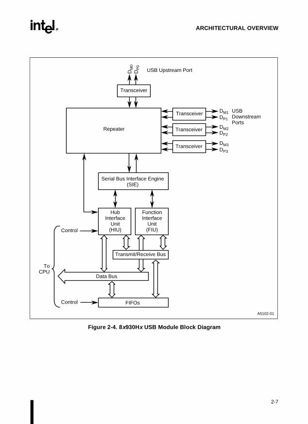
ARCHITECTURAL OVERVIEW
Figure 2-4. 8 x930Hx USB Module Block Diagram
A5102-01
DP3
DM3
DP2
DM2
DP1
DM
0 D
P0
DM1
Repeater
USB Upstream Port
USB Downstream Ports
Serial Bus Interface Engine (SIE)
Transceiver
Transceiver
Transceiver
Hub Interface
Unit (HIU)
Function Interface
Unit (FIU)
Control
Control
FIFOs
Data Bus
To CPU
Transmit/Receive Bus
Transceiver
2-7

8x930Ax, 8x930Hx USER’S MANUAL
he busegister
inglenfigure Ine fetchles” on
double
on-ll and
Figure 2-5. The CPU
2.2 MICROCONTROLLER CORE
The microcontroller core contains the CPU, the clock and reset unit, the interrupt handler, tinterface, and the peripheral interface. The CPU contains the instruction sequencer, ALU, rfile, and data memory interface.
2.2.1 CPU
Figure 2-5 is a functional block diagram of the CPU (central processor unit). The 8x930 fetchesinstructions from on-chip code memory two bytes at a time, or from external memory in sbytes. The instructions are sent over the 16-bit code bus to the execution unit. You can cothe 8x930 to operate in page mode for accelerated instruction fetches from external memory.page mode, if an instruction fetch is to the same 256-byte “page” as the previous fetch, threquires one state time rather than two state times. See “State Time and Peripheral Cycpage 2-9.
The 8x930 register file has forty registers, which can be accessed as bytes, words, and words. As in the MCS®51 architecture, registers 0–7 consist of four banks of eight registers each,where the active bank is selected by the program status word (PSW) for fast context switches.Refer to Chapter 3, “8x930 Register File” or see Figure 5-2 on page 5-17.
The 8x930 is a single-pipeline machine. When the pipeline is full and code is executing fromchip code memory, an instruction is completed every state time. When the pipeline is fu
A4272-01
SRC2 (8)
Code Address (24)Code Bus (16)
SRC1 (8)
Instruction Sequencer
DST (16)
ALUData
Memory Interface
Register File
Data Address (24)
Data Bus (8)
Interrupt Handler
2-8

ARCHITECTURAL OVERVIEW
gnal),
and
n-chipd
he in-auseull- the ex-or low
-d once
code is executing from external memory (with no wait states and no extension of the ALE sian instruction is completed every two state times.
2.2.2 Clock and Reset Unit
Figure 2-6 on page 2-9 shows the internal clock circuitry of the 8x930. The timing waveform atXTAL1 can be provided by:
• an on-chip oscillator employing an external crystal/resonator connected across XTAL1XTAL2
• an external frequency source connected to XTAL1
“Clock Sources” on page 14-2 discusses the requirements for external-clock signals and ooscillators. Power management options – idle, powerdown, and low-clock mode – are discussein Chapter 15, “Special Operating Modes.”
Device pins PLLSEL2:0 determine the USB operating rate (full speed or low speed) and tternal frequency (FCLK) distributed to the CPU and on-chip peripherals. See Table 2-4. Becof its hub capability, the 8x930Hx (including the embedded function) always operates as a fspeed USB device. Root port data transfers are always full speed. Data transfer rates onternal downstream ports are matched to the type of USB device attached (i.e., full speed speed). For full speed operation, the PLL provides the 4X USB sampling rate.
2.2.2.1 State Time and Peripheral Cycles
The basic unit of time for 8x930 microcontrollers is the state time (or state). States are dividedinto two phases identified as phase 1 and phase 2. See Figures 2-7 and 2-8. The 8x930 on-chipperipherals operate on a peripheral cycle, which is six state times. A specific time within a peripheral cycle is denoted by its state and phase. For example, the PCA timer is incrementeeach peripheral cycle in phase 2 of state 5 (denoted as S5P2).
Figure 2-6. Clock Circuit
Clock Generator
A5135-01
XTAL1
XTAL2
FOSC (6 or 12 MHz)
PCON.0 (Idle Mode)
IDLPCON.1
(Powerdown)
0
1
PD
÷ 2
1 02PLLSEL
FCLK
CPU
On-chip Peripherals
Internal Clock
PCON.5 (Low-clock Mode)
LC
0
1
3 MHz
2-9

8x930Ax, 8x930Hx USER’S MANUAL
re two (full
s
n inice re-
al Op-
pin,
refer to
As shown in Table 2-4 and Figure 2-7, when PLLSEL2:0 = 001 or 100 (low speed), there aTOSC periods per state. As shown in Table 2-4 and Figure 2-8, when PLLSEL2:0 = 110speed), there is one TOSC period per state. See “Low-clock Mode” below.
As shown in Table 2-4 the internal clock frequency (FCLK) distributed to the CPU and peripheral(3, 6, or 12 MHz) is a function of PLLSEL2:0 and FOSC. Note that in Figure 2-6, for PLLSEL2:0= 110 (full speed), the two-to-one divider stage is bypassed and FCLK = FOSC = 12 MHz.
2.2.2.2 Low-clock Mode
A special power-reduction mode (low-clock mode) overrides the timing definitions give“State Time and Peripheral Cycles” above and Figures 2-7 and Figures 2-8. Following devset, the CPU and on-chip peripherals operate in low-clock mode (FCLK = 3 MHz) until the LC bitin PCON is cleared. During low-clock mode, there are four TOSC periods per state for PLLSEL2:0= 001 or 100. Low-clock mode does not affect the USB rate. Also see Chapter 15, “Specierating Modes.”
2.2.2.3 Reset Unit
The reset unit resets the 8x930 to a known state. A chip reset is initiated by asserting the RSTby a USB-initiated reset, or by allowing the watchdog timer to time out. The 8x930Ax can be pro-grammed so a USB-initiated reset does not cause a chip reset. For information on resets Chapter 14, “Minimum Hardware Setup”.
Table 2-4. 8x930 Operating Frequency
DevicePLLSEL2:0
(Pins 43, 42, 44)(1)
XTAL1Frequency
(FOSC)
USB Rate(2)
Internal Frequency
(FCLK)(3)
XTAL1 Clocks per
State(TOSC/state)
(5)
Comments
8x930Ax 001 6 Mhz 1.5 Mbps (Low Speed)
3 Mhz 2 (4) PLL Off
8x930Ax 100 12 Mhz 1.5 Mbps (Low Speed)
6 Mhz (4) 2 (4) PLL Off
8x930Ax8x930Hx
110 12 Mhz 12 Mbps (Full Speed)
12 Mhz (4) 1 PLL On
NOTES:1. Other PLLSEL2:0 combinations are not valid.2. The sampling rate is 4X the USB rate.3. The internal frequency, FCLK = 1/TCLK, is the clock signal distributed to the CPU and the on-chip
peripherals,4. Following device reset, the CPU and on-chip peripherals operate in low-clock mode (FCLK = 3 Mhz)
until the LC bit in the PCON register is cleared. In low clock mode, there are four TOSC periods per state for PLLSEL2:0 = 100 or 110. Low-clock mode does not affect the USB rate.
5. The number of XTAL1 clock periods per state (TOSC/state) depends on PLLSEL2:0 and the LC bit.
2-10

ARCHITECTURAL OVERVIEW
Figure 2-7. Clocking Definitions (Low Speed)
Figure 2-8. Clocking Definitions (Full Speed)
TOSC
State 2
P1 P2State 1
P1 P2State 3
P1 P2State 4
P1 P2State 5
P1 P2
State 6
P1 P2
Peripheral Cycle
2 TOSC = State Time
XTAL1
XTAL1
P1 P2
Phase 1 Phase 2
A2604-02
TOSC
State
P1
Peripheral Cycle (6 States)
1 TOSC = State Time
XTAL1
XTAL1
P1
A5086-01
P2 P1 P2 P1 P2 P1 P2 P1 P2 P1 P2
1 2 3 4 5 6
P2
2-11

8x930Ax, 8x930Hx USER’S MANUAL
e the in-nfor a
0H. lo--
thatge 4-9gura-
em-dress-
B de-he
(pinsor-al
SFRs
scribependix-
e. The
func-O
2.2.3 Interrupt Handler
The interrupt handler can receive interrupt requests from eleven maskable sources and the TRAPinstruction. When the interrupt handler grants an interrupt request, the CPU discontinues thnor-mal flow of instructions and branches to a routine that services the source that requestedterrupt. You can enable or disable the interrupts individually (except for TRAP) and you caassign one of four priority levels to each interrupt. Refer to Chapter 6, “Interrupt System,” detailed description.
2.3 ON-CHIP MEMORY
For ROM devices, the 8x930 provides on-chip program memory beginning at location FF:000See Table 2-1 for memory options. Following chip reset, the first instruction is fetched fromcation FF:0000H. (For devices without ROM, instruction fetches are always from external memory. Following chip reset, the first instruction is fetched from the external memory locationcorresponds to internal address FF:0000H. Figure 4-5 on page 4-8 and Figure 4-6 on pashow how addresses in region FF: map into external memory for various memory confitions.)
The 8x930 provides on-chip data RAM beginning at location 00:0020H (just above the four banksof registers R0–R7 which occupy the first 32 bytes of the memory space). See Table 2-1 for mory options. Data RAM locations can be accessed with direct, indirect, and displacement ading. Ninety-six of these locations (20H–7FH) are bit addressable.
2.4 UNIVERSAL SERIAL BUS MODULE
The USB module operates in conjunction with the CPU to provide the capabilities of a USvice. The 8x930Ax USB module provides a function interface for one USB function. T8x930Hx USB module supports one USB function and in addition provides a USB hub capability.
The 8x930 USB module communicates with the host PC by means of upstream data port 0DP0, DM0). In addition to the upstream port, the 8x930Hx has three external downstream ports fbus expansion (pins DP1, DM1, DP2, DM2, DP3, DM3) and an internal downstream port for communicating with the embedded function. The 8x930 provides on-chip transceivers for each externUSB port.
Operation of the USB module is controlled through the use of special function registers (SFRs).SFRs associated with the function interface are described in Chapter 7, “USB Function.” associated with USB hub operations are described in Chapter 8, “USB Hub.” Interrupt SFRs aredescribed in Chapter 6, “Interrupt System.” Register definition tables in these chapters deregister usage and define the register bits. The register definition tables also appear in ApC in alphabetical order. Memory maps of the 8x930Ax and 8x930Hx SFRs are presented in Chapter 3, “Address Spaces” and Appendix C.
Data transfers with the host are made to/from endpoint pairs (EPPs) on the USB modul8x930Hx provides four function endpoint pairs and two hub endpoint pairs. The 8x930Ax can beprogrammed to support either four or six function endpoint pairs. Table 2-5 lists the hub andtion endpoint pairs available on the 8x930Hx along with the associated transmit and receive FIFdata buffers. Except for hub endpoints 0 and 1, Table 2-5 also to applies to the 8x930Ax when the4EPP option is selected. Table 2-6 lists the endpoint pairs available on the 8x930Ax when the
2-12

ARCHITECTURAL OVERVIEW
air in-
” sec-
“Tim-
6EPP option is selected. The value in the EPINDEX register determines the endpoint pvolved in any given data transfer operation (Tables 2-5 and Table 2-6).
A complete description of the USB can be found in Universal Serial Bus Specification. For a de-scription of the transceiver see the “Driver Characteristics” and “Receiver Characteristicstions of the “Electrical” chapter of the Universal Serial Bus Specification. For electricalcharacteristics and data signal timing, see the “Bus Timing/Electrical Characteristics” and ing Diagram” sections of the same chapter.
Table 2-5. Endpoint Pairs for 8 x930Hx and 8x930Ax (4EPP Option)
EPINDEX Endpoint Pair TransmitFIFOs
ReceiveFIFOs
FIFO Size Select (1)
0000 0000 Function Endpoint 0 (Control) 16 bytes 16 bytes XX
0000 0001 Function Endpoint 1 256 bytes 256 bytes 0 0
512 bytes 512 bytes 0 1
1024 bytes 0 bytes 1 0
0 bytes 1024 bytes 1 1
0000 0010 Function Endpoint 2 16 bytes 16 bytes XX
0000 0011 Function Endpoint 3 16 bytes 16 bytes XX
1000 0000 Hub Endpoint 0 (Control) (2) 16 bytes 16 bytes XX
1000 0001 Hub Endpoint 1 (2), (3) N/A N/A XX
NOTE:1. Bits FFSZ1:0 (TXCON.6:5) specify the size of the transmit and receive FIFOs for function
endpoint 1.2. Hub endpoints are not applicable to the 8X930Ax.3. Hub endpoint 1 assembles status-change information in a buffer register (TXDAT) and
transmits it to the host PC. Hub endpoint 1 does not require FIFOs.
Table 2-6. Endpoint Pairs for 8 x930Ax (6EPP Option)
EPINDEX Endpoint Pair TransmitFIFOs
ReceiveFIFOs
FIFO Size Select (1)
0000 0000 Function Endpoint 0 (Control) 16 bytes 16 bytes XX
0000 0001 Function Endpoint 1 256 bytes 256 bytes 0 0
0000 0010 Function Endpoint 2 32 bytes 32 bytes XX
0000 0011 Function Endpoint 3 32 bytes 32 bytes XX
0000 0100 Function Endpoint 4 (2) 32 bytes 32 bytes XX
0000 0101 Function Endpoint 5 (2) 16 bytes 16 bytes XX
NOTE:1. Bits FFSZ1:0 (TXCON.6:5) specify the size of the transmit and receive FIFOs for function
endpoint 1. For the 6EPP option, use FFSZ1:0 = 00.2. On the 8x930Ax, setting the SIXEPPEN bit in the EPCONFIG register selects the six-
endpoint option (6EPP). Function endpoints 4 and 5 are available only when the 6EPP option is selected. Early sample devices did not have this feature.
2-13

8x930Ax, 8x930Hx USER’S MANUAL
en theE), themmu-es the
bulk.
host
IFOs,olthe
onfig-ceive
have
, and
s not
datal data
ability.
2.4.1 The 8x930Ax USB Module
Figure 2-3 on page 2-6 shows the main functional blocks of the 8x930Ax USB module and howthey interface with the CPU. The USB function interface manages communications betwehost PC and the USB function. This interface consists of the serial bus interface engine (SIfunction interface unit (FIU), and the transmit and receive FIFOs. The SIE handles the conication protocol of the universal serial bus, and the FIU handles data transfers and providinterface between the SIE and the 8x930Ax CPU.
The 8x930Ax function interface, which can be programmed to have either four or six endpointpairs, supports all four types of USB data transfer: control, isochronous, interrupt, and Function endpoint 1 handles only control data transfers, whereas function endpoints 1 through 5handle all four data transfer types.
2.4.1.1 Serial Bus Interface Engine (SIE)
The SIE is the USB protocol interpreter for communications between the 8x930Hx and the hostPC over the USB lines. It provides serial-to-parallel conversion for data transfers from theand parallel-to-serial conversion for data transfers to the host. For additional information on theSIE, see “SIE Details” on page 7-33.
2.4.1.2 Function Interface Unit (FIU)
The FIU manages data movement within the USB module. It controls the operation of the Fmonitors the status of the data transactions, and at the appropriate moment transfers event contrto the CPU through an interrupt request. The exact nature of a data transaction depends on type of data transfer and the initial conditions of the transmit and receive FIFOs.
2.4.1.3 Function FIFOs
Each endpoint pair contains a transmit FIFO and a receive FIFO. See Table 2-5 for FIFO curations. Transmit FIFOs are written by the CPU, then read by the FIU for transmission. ReFIFOs are written by the FIU following reception, then read by the CPU. All transmit FIFOs the same architecture, and all receive FIFOs have the same architecture.
2.4.2 The 8x930Hx USB Module
Figure 2-4 on page 2-7 shows the main functional blocks of the 8x930Hx USB module and howthey interface with CPU. As on the 8X930Ax USB module described above, The SIE, FIUfunction FIFOs comprise the function interface. The 8x930Hx function interface is similar to thatof the 8x930Ax. See “The 8x930Ax USB Module” on page 2-14. There are three main differenc-es: the 8x930Hx function interface is accessed via the internal downstream port, and it doehave the six-endpoint pair option nor the separate USB reset feature.
The 8x930Hx function interface has four endpoint pairs. It supports all four types of USB transfer: control, isochronous, interrupt, and bulk. Function endpoint 0 handles only controtransfers, whereas function endpoints 1, 2, and 3 handle all four data transfer types.
The repeater, the SIE, the hub interface unit (HIU), and the hub FIFOs provide the hub capThe hub interface has two endpoint pairs. Hub endpoint 0 supports only control data transfers.Hub endpoint 1 is used to transmit hub status change information to the host PC.
2-14

ARCHITECTURAL OVERVIEW
d hube en-
n-am rforms
n and
a frompos-on.The
fers toplete
intainonse to
, “USB
nsfersading
ata
rface.USB re- is im-e is
8x930Hx USB hub operations are divided into two categories: hub repeater operations ancontroller operations. The hub controller is split among four modules: the serial bus interfacgine, the hub interface unit, the hub endpoint 0 transmit and receive FIFOs, and the 8x930HxCPU. (See Chapter 8.) The following subsections discuss the role of each module.
2.4.2.1 Hub Repeater
The repeater is the connectivity manager for the 8X930Hx. It detects the connection or disconection of devices on the external downstream ports and manages the upstream/downstrecon-nectivity for data packets. It keeps track of hub port status, manages connectivity, and pepower management for external down stream ports. The repeater supports both full-speed (12Mbps) and low-speed (1.5 Mbps) data traffic. The repeater also controls bus fault detectiorecovery. Downstream port control is managed primarily by the HIU.
2.4.2.2 Serial Bus Interface Engine (SIE)
The SIE is the USB communication protocol interpreter. It places data on and accepts datthe bus. On the 8x930Hx, the hub interface and the function interface share the SIE. This is sible because the host communicates with only a single device during any one transactiSIE is permanently attached to the internal downstream port. The SIE provides serial-to-parallelconversion for data transfers from the host and parallel-to-serial conversion for data transthe host. For additional information on the SIE, see “SIE Details” on page 7-33. For comfunctional, signal, and timing information, refer to the USB Function SIE Interface Specification.
2.4.2.3 Hub Interface Unit (HIU)
The HIU uses special function registers (SFRs) to control the operation of the hub and to mathe status of the hub and its downstream ports. Control SFRs are set by firmware in respUSB requests. Status SFRs are set by the repeater hardware. Refer to Chapter 8, “USB Hub”, andChapter 9, “USB Programming Models,” for a discussion on the use of the HIU SFRs.
2.4.2.4 Hub FIFOs
Hub FIFOs operate in the same manner as the function interface FIFOs. See Chapter 7Function.” Hub endpoint 0 handles only control data transfers. It is implemented with 16-bytetransmit and receive FIFO data buffers. The maximum packet size for hub control data trais eight bytes. Data received from the USB for endpoint 0 is stored in the receive FIFO for reby firmware. Data to be sent to the host from hub endpoint 0 is loaded into the transmit FIFO.
Hub endpoint 1 transmits single-byte interrupt tokens to the host and does not have FIFO dbuffers.
2.4.2.5 8x930Hx CPU
The CPU runs the firmware associated with the operation of the hub and the function inteThe CPU reads the receive FIFOs, loads the transmit FIFOs, and decodes and executes quests for the hub. Control transaction stages are also tracked by firmware. Hub operationplemented by reading and writing SFRs in the HIU. Operation of the function interfacimplemented by reading and writing SFRs in the FIU.
2-15

8x930Ax, 8x930Hx USER’S MANUAL
func-FRs).able
me ofr gen-uests.
eeginsormaln oc-ethapter
- output mod-
-
odes.in
simul-e of 11can be 2, you
e over-
2.5 ON-CHIP PERIPHERALS
The on-chip peripherals reside outside the microcontroller core. They perform specializedtions in hardware. Firmware controls the peripherals via their special function registers (SThe 8x930 has four peripherals: the watchdog timer, the timer/counter unit, the programmcounter array (PCA), and the serial I/O port.
2.5.1 Timer/Counters and Watchdog Timer
The timer/counter unit has three timer/counters, which can be clocked by the oscillator (for timeroperation) or by an external input (for counter operation). You can set up an 8-bit, 13-bit, or 16-bit timer/counter. You can program them for special applications, such as capturing the tian event on an external pin, outputting a programmable clock signal on an external pin, oerating a baud rate for the serial I/O port. Timer/counter events can generate interrupt req
The watchdog timer is a circuit that automatically resets the 8x930 in the event that a hardwaror firmware operation fails to complete. When enabled by firmware, the watchdog timer brunning, and unless firmware intervenes, the timer overflows and initiates a chip reset. In noperation, firmware periodically clears the timer register to prevent the reset. If a malfunctiocurs and firmware fails to clear the timer, the resulting chip reset disables the timer and rurnsthe system to a known state. The watchdog timer and the timer/counters are described in C11, “Timer/Counters and Watchdog Timer.”
2.5.2 Programmable Counter Array (PCA)
The programmable counter array (PCA) has its own timer and five capture/compare modules thatperform several functions: capturing (storing) the timer value in response to a transition on an input pin; generating an interrupt request when the timer matches a stored value; toggling anpin when the timer matches a stored value; generating a programmable PWM (pulse widthulator) signal on an output pin; and serving as a firmware watchdog timer. Chapter 12, “Programmable Counter Array,” describes this peripheral in detail.
2.5.3 Serial I/O Port
The serial I/O port provides one synchronous and three asynchronous communication mThe synchronous mode (mode 0) is half-duplex: the serial port outputs a clock signal on one pand transmits or receives data on another pin.
The asynchronous modes (modes 1–3) are full-duplex (i.e., the port can send and receivetaneously). Mode 1 uses a serial frame of 10 bits: a start bit, 8 data bits, and a stop bit. Thbaudrate is generated by the overflow of timer 1 or timer 2. Modes 2 and 3 use a serial framebits: a start bit, eight data bits, a programmable ninth data bit, and a stop bit. The ninth bit used for parity checking or to specify that the frame contains an address and data. In modecan use a baud rate of 1/32 or 1/64 of the oscillator frequency. In mode 3, you can use thflow from timer 1 or timer 2 to determine the baud rate.
2-16

ARCHITECTURAL OVERVIEW
onmentelf or a another
perat-
Reset
In its asynchronous modes (modes 1–3) the serial port can operate as a slave in an envirwhere multiple slaves share a single serial line. It can accept a message intended for itsmessage that is being broadcast to all of the slaves, and it can ignore a message sent toslave.
2.6 OPERATING CONDITIONS
The 8x930 is designed for a commercial operating environment and to accommodate the oing rates of the USB interface. For detailed specifications, refer to the current 8x930 UniversalSerial Bus Microcontroller datasheet. For USB module operating rates, see “Clock and Unit” on page 2-9.
2-17


3Address Spaces


ace, and
chitec-ing from
CHAPTER 3ADDRESS SPACES
The 8x930 has three address spaces: a memory space, a special function register (SFR) spa register file. This chapter describes these address spaces as they apply to the 8x930. It also dis-cusses the compatibility of the MCS® 251 architecture and the MCS® 51 architecture in terms oftheir address spaces.
3.1 MCS® 251 ARCHITECTURE ADDRESS SPACES
Figure 3-1 shows the memory space, the SFR space, and the register file for MCS 251 arture. (The address spaces are depicted as being eight bytes wide with addresses increasleft to right and from bottom to top.)
Figure 3-1. MCS® 251Architecture Address Spaces
A4100-01
FF:FFFFH
SFR Space 512 Bytes
Memory Address Space 16 Mbytes
00:0000H 0
Register File 64 Bytes
7
63
S:000H
S:1FFH
00:0007H
S:007H
3-1
8x930Ax, 8x930Hx USER’S MANUAL
e
at lo-ytes of
file areanks,
space.
resseshemem-ge
CS
lity of
cationsnly bete codewith thethe
eight
s spaces
It is convenient to view the unsegmented, 16-Mbyte memory space as consisting of 256 64-Kbytregions, numbered 00: to FF:.
NOTEThe memory space in the 8x930 is unsegmented. The 64-Kbyte “regions” 00:, 01:, ..., FF: are introduced only as a convenience for discussions. Addressing in the 8x930 is linear; there are no segment registers.
On-chip RAM is located at the bottom of the memory space, beginning at location 00:0000H. Thefirst 32 bytes (00:0000H–00:001FH) provide storage for a part of the register file. The on-chip,general-purpose data RAM resides just above this, beginning at location 00:0020H.
On-chip ROM (code memory) is located in the top region of the memory space, beginningcation FF:0000H. Following device reset, execution begins at this address. The top eight bregion FF: are reserved for the configuration array.
The register file has its own address space (Figure 3-1). The 64 locations in the register numbered decimally from 0 to 63. Locations 0–7 represent one of four switchable register beach having eight registers. The 32 bytes required for these banks occupy locations 00:0000H–00:001FH in the memory space. Register file locations 8–63 do not appear in the memory See “8x930 Register File” on page 3-9 for a further description of the register file.
The SFR space accommodates up to 512 eight-bit special function registers with addS:000H–S:1FFH. SFRs implemented in the 8x930 are shown in Table 3-6 on page 3-10. In tMCS 251 architecture, use the prefix “S:” with SFR addresses to distinguish them from the ory space addresses 00:0000H–00:01FFH. See “Special Function Registers (SFRs)” on pa3-15for details on the SFR space.
3.1.1 Compatibility with the MCS ® 51 Architecture
The address spaces in the MCS 51 architecture† are mapped into the address spaces in the M251 architecture. This mapping allows code written for MCS 51 microcontrollers to run on MCS251 microcontrollers. (Chapter 5, “Programming Considerations” discusses the compatibithe two instruction sets.)
Figure 3-2 shows the address spaces for the MCS 51 architecture. Internal data memory lo00H–7FH can be addressed directly and indirectly. Internal data locations 80H–FFH can oaddressed indirectly. Directly addressing these locations accesses the SFRs. The 64-Kbymemory has a separate memory space. Data in the code memory can be accessed only MOVC instruction. Similarly, the 64-Kbyte external data memory can be accessed only with MOVX instruction.
The register file (registers R0–R7) comprises four switchable register banks, each havingregisters. The 32 bytes required for the four banks occupy locations 00H–1FH in the on-chip datamemory.
Figure 3-3 shows how the address spaces in the MCS 51 architecture map into the addresin the MCS 251 architecture; details are listed in Table 3-1.
† MCS®51 Microcontroller Family User’s Manual (Order Number: 272383)
3-2

ADDRESS SPACES
codected to-
The 64-Kbyte code memory for MCS 51 microcontrollers maps into region FF: of the memoryspace for MCS 251 microcontrollers. Assemblers for MCS 251 microcontrollers assemblefor MCS 51 microcontrollers into region FF:, and data accesses to code memory are direthis region. The assembler also maps the interrupt vectors to region FF:. This mapping is transparent to the user; code executes just as before, without modification.
Figure 3-2. Address Spaces for the MCS ® 51 Architecture
External Data (MOVX)
FFFFH
0000H
A4139-01
00H
FFH
80H7FH
Code (MOVC)
Internal Data (direct, indirect)
Register File
SFRs (direct)
Internal Data (indirect)
0000H
FFFFH
80H
FFH
R7R0
3-3

8x930Ax, 8x930Hx USER’S MANUAL
Figure 3-3. Address Space Mappings MCS ® 51 Architecture to MCS ® 251 Architecture
Table 3-1. Address Mappings
Memory Type
MCS® 51 Architecture MCS ® 251 Architecture
Size Location DataAddressing Location
Code 64 Kbytes 0000H–FFFFH Indirect using MOVC instr. FF:0000H–FF:FFFFH
External Data 64 Kbytes 0000H–FFFFH Indirect using MOVX instr. 01:0000H–01:FFFFH
Internal Data 128 bytes 00H–7FH Direct, Indirect 00:0000H–00:007FH
128 bytes 80H–FFH Indirect 00:0080H–00:00FFH
SFRs 128 bytes S:80H–S:FFH Direct S:080H–S:0FFH
Register File 8 bytes R0–R7 Register R0–R7
FFH
SFR Space 512 Bytes
Memory Address Space 16 Mbytes
S:000H
MCS 51 Architecture Code Memory
MCS 51 Architecture External Data Memory
MCS 51 Architecture Internal Data Memory
FFFFH
00H
0000H
FFFFH
0000H
MCS 51 Architecture SFRs
00:0000H
01:0000H
02:0000H
FF:0000H
A4133-01
S:100H
S:1FFH
8
Register File 64 Bytes
MCS 51 Architecture R. F.00
63
S:07FH80H
FFH
7
3-4

ADDRESS SPACES
-gisterThe re-e 3-3. 51
rchi-entical
ed toarchi-perions in
ace of
ad-S 251side inpped
ae to the
ber of
evice
uturee the
nfigu-
of mem- RAM
The 64-Kbyte external data memory for MCS 51 microcontrollers is mapped into the memory region specified by bits 16–23 of the data pointer DPX, i.e., DPXL. DPXL is accessible as refile location 57 and also as the SFR at S:084H (see “Dedicated Registers” on page 3-12). set value of DPXL is 01H, which maps the external memory to region 01: as shown in FigurYou can change this mapping by writing a different value to DPXL. A mapping of the MCSmicrocontroller external data memory into any 64-Kbyte memory region in the MCS 251 atecture provides complete run-time compatibility because the lower 16 address bits are idin the two address spaces.
The 256 bytes of on-chip data memory for MCS 51 microcontrollers (00H-FFH) are mappaddresses 00:0000H-00:00FFH to ensure complete run-time compatibility. In the MCS 51 tecture, the lower 128 bytes (00H-7FH) are directly and indirectly addressable; however the up128 bytes are accessible by indirect addressing only. In the MCS 251 architecture, all locatregion 00: are accessible by direct, indirect, and displacement addressing (see “8x930 MemorySpace” on page 3-5).
The 128-byte SFR space for MCS 51 microcontrollers is mapped into the 512-byte SFR spthe MCS 251 architecture starting at address S:080H, as shown in Figure 3-3. This provides com-plete compatibility with direct addressing of MCS 51 microcontroller SFRs (including bit dressing). The SFR addresses are unchanged in the new architecture. In the MCarchitecture, SFRs A, B, DPL, DPH, and SP (as well as the new SFRs DPXL and SPH) rethe register file for high performance. However, to maintain compatibility, they are also mainto the SFR space at the same addresses as in the MCS 51 architecture.
3.2 8x930 MEMORY SPACE
Figure 3-4 shows the logical memory space for the 8x930 microcontroller. The usable memoryspace of the 8x930 consists of four 64-Kbyte regions: 00:, 01:, FE:, and FF:. Code can executefrom all four regions; code execution begins at FF:0000H. Regions 02:-FD are reserved. Redinga location in the reserved area returns an unspecified value. Firmware can execute a writreserved area, but nothing is actually written.
All four regions of the memory space are available at the same time. The maximum numexternal address lines is 18, which limits external memory to a maximum of four regions (256Kbytes). See “Configuring the External Memory Interface” on page 4-7, and “External MemoryDesign Examples” on page 16-17.
Locations FF:FFF8H–FF:FFFFH are reserved for the configuration array (see Chapter 4, “DConfiguration”). The two configuration bytes for the 8x930 are accessed at locations FF:FFF8Hand FF:FFF9H; locations FF:FFFAH–FF:FFFFH are reserved for configuration bytes in fproducts. Do not attempt to execute code from locations FF:FFF8H–FF:FFFFH. Also, secaution on page 4-3 regarding execution of code from locations immediately below the coration array.
Figure 3-4 also indicates the addressing modes that can be used to access different areasory. The first 64 Kbytes can be directly addressed. The first 96 bytes of general-purpose(00:0020H–00:007FH) are bit addressable. Chapter 5, “Programming Considerations,” discussesaddressing modes.
3-5

8x930Ax, 8x930Hx USER’S MANUAL
Figure 3-4. 8 x930 Address Space
A4385-01
01:FFFFH
FE:FFFFH
FF:FFFFH
01:0000H
FE:0000H
FF:0000H
Memory Address Space 16 Mbytes
00:0080H
00:0020H00:007FH
00:0000H 00:001FH
00:FFFFH
Indirect and Displacement Addressing (16 Mbytes)
Direct Addressing (64 Kbytes)
Bit Addressing (96 Bytes)Register Addressing
(32 Bytes)
Regions 02–FD are Reserved
3-6

ADDRESS SPACES
Figure 3-5. Hardware Implementation of the 8 x930 Address Space
A5209-01
01:FFFFH
FE:FFFFH
FF:FFF7H
01:0000H
FE:0000H
FF:0000H
External Memory
External Memory
Registers R0-R7
External Memory
00:0000H
00:FFFFH
On-chip ROM 8 or 16 Kbytes
On-chip RAM 1024 Bytes
External Memory
† Eight-byte configuration array (FF:FFF8H - FF:FFFFH) †† Four banks of registers R0-R7 (32 bytes, 00:0000H - 00:001FH)
†
††
Regions 02–FD are Reserved
3-7

8x930Ax, 8x930Hx USER’S MANUAL
rnal
m on-ations
FF:.e. On- datacution
nly if
p code code
Figure 3-5 shows how areas of the memory space are implemented by on-chip RAM and extememory. The first 32 bytes of on-chip RAM store banks 0–3 of the register file (see “8x930 Reg-ister File” on page 3-9).
3.2.1 On-chip General-purpose Data RAM
On-chip RAM provides general data storage (Figure 3-5). Instructions cannot execute frochip data RAM. The data is accessible by direct, indirect, and displacement addressing. Loc00:0020H–00:007FH are also bit addressable.
3.2.2 On-chip Code Memory
The 8x930 is available with 0, 8 or 16 Kbytes of on-chip ROM located in memory region (Figure 3-5). Table 2-1 on page 2-3 lists the amount of on-chip code memory for each devicchip ROM is intended primarily for code storage, although its contents can also be read aswith the indirect and displacement addressing modes. Following a chip reset, program exebegins at FF:0000H. Chapter 17, “Verifying Nonvolatile Memory,” describes the procedure forverifying the contents of on-chip ROM.
A code fetch within the address range of the on-chip ROM accesses the on-chip ROM oEA# = 1. For EA# = 0, a code fetch in this address range accesses external memory. The value ofEA# is latched when the chip leaves the reset state. Code is fetched faster from on-chimemory than from external memory. Table 3-2 lists the minimum times to fetch two bytes offrom on-chip memory and external memory.
NOTEIf your program executes exclusively from on-chip ROM (not from external memory), beware of executing code from the upper eight bytes of the on-chip ROM (FF:1FF8H–FF:1FFFH for 8 Kbytes, FF:3FF8H–FF:3FFFH for 16 Kbytes). Because of its pipeline capability, the 8x930 may attempt to prefetch code from external memory (at an address above FF:1FFFH/ FF:3FFFH) and thereby disrupt I/O ports 0 and 2. Fetching code constants from these eight bytes does not affect ports 0 and 2.
If your program executes from both on-chip ROM and external memory, code can be placed in the upper eight bytes of on-chip ROM. As the 8x930 fetches bytes above the top address in the on-chip ROM, code fetches automatically become external bus cycles. In other words, the rollover from on-chip ROM to external code memory is transparent to the user.
Table 3-2. Minimum Times to Fetch Two Bytes of Code
Type of Code Memory State Times
On-chip Code Memory 1
External Memory (page mode) 2
External Memory (nonpage mode) 4
3-8

ADDRESS SPACES
of thea
gt hold
n
eferred
ted as
These
ed
, as il-
ddresscessi-le 3-3.
dd.
3.2.2.1 Accessing On-chip Code Memory in Region 00:
Devices with 16 Kbytes of on-chip code memory can be configured so that the upper half on-chip code memory can also be read as data at locations at the top of region 00: (see “MppingOn-chip Code Memory to Data Memory (EMAP#)” on page 4-14). That is, locations FF:2000H–FF:3FFFH can also be accessed at locations 00:E000H–00:FFFFH. This is useful for accessincode constants stored in ROM. Note, however, that all of the following three conditions musfor this mapping to be effective:
• The device is configured with EMAP# = 0 in the UCONFIG1 register (See Figure 4-3 opage 4-5).
• EA# = 1.
• The access to this area of region 00: is a data read, not a code fetch.
If one or more of these conditions do not hold, accesses to the locations in region 00: are rto external memory.
3.2.3 External Memory
Regions 01:, FE:, and portions of regions 00: and FF: of the memory space are implemenexternal memory (Figure 3-5). For discussions of external memory, see “Configuring the ExternalMemory Interface” on page 4-7, and Chapter 16, “External Memory Interface.”
3.3 8x930 REGISTER FILE
The 8x930 register file consists of 40 locations: 0–31 and 56–63, as shown in Figure 3-6. locations are accessible as bytes, words, and dwords, as described in “Byte, Word, and DwordRegisters” on page 3-12.” Several locations are dedicated to special registers (see “DedicatRegisters” on page 3-12); the remainder are general-purpose registers.
Register file locations 0–7 actually consist of four switchable banks of eight registers eachlustrated in Figure 3-7 on page 3-11. The four banks are implemented as the first 32 bytes of on-chip RAM and are always accessible as locations 00:0000H–00:001FH in the memory aspace.† Only one of the four banks is accessible via the register file at a given time. The acble, or “active,” bank is selected by bits RS1 and RS0 in the PSW register, as shown in Tab(The PSW is described in “Program Status Words” on page 5-15.”) This bank selection can beused for fast context switches.
Register file locations 8–31 and 56–63 are always accessible. These locations are implementeas registers in the CPU. Register file locations 32–55 are reserved and cannot be accesse
† Because these locations are dedicated to the register file, they are not considered a part of the general-purpose, 1-Kbyte, on-chip RAM (locations 00:0020H–00:041FH).
3-9

8x930Ax, 8x930Hx USER’S MANUAL
Figure 3-6. The Register File
A4099-01
DR4DR0
DR12DR8
15141312111098
2322212019181716
3130292827262524
Locations 32-55 are Reserved
6362616059585756
R7R6R5R4R3R2R1R0
R15R14R13R12R11R10R9R8
DR20DR16
DR28DR24
WR6WR4WR2WR0
WR14WR12WR10WR8
WR22WR20WR18WR16
WR30WR28WR26WR24
DR60 = SPXDR56 = DPX
Dword Registers
Word Registers
Byte Registers
Register File
76543210
76543210
Banks 0-3
Note: R10 = B R11 = ACC
3-10

ADDRESS SPACES
Figure 3-7. Register File Locations 0–7
Table 3-3. Register Bank Selection
Bank Address RangePSW Selection Bits
RS1 RS0
Bank 0 00H–07H 0 0
Bank 1 08H–0FH 0 1
Bank 2 10H–17H 1 0
Bank 3 18H–1FH 1 1
A4215-01
Register File
0 1 2 3 4 5 6 78
63
Memory Address Space
FF:FFFFH
00:0020H
18H 1FH10H 17H08H 0FH00H 07H
Banks 0–3
0 1 2 3 4 5 6 70 1 2 3 4 5 6 7
0 1 2 3 4 5 6 70 1 2 3 4 5 6 7PSW bits RS1:0
select one bank to be accessed via the register file.
Banks 0–3 accessible in memory address space
3-11

8x930Ax, 8x930Hx USER’S MANUAL
nd/or ad byte
ressablead-ise the
L of DPX
ed
e ash
ne state
r datanMCS
r
3.4 BYTE, WORD, AND DWORD REGISTERS
Depending on its location in the register file, a register is addressable as a byte, a word, adword, as shown on the right side of Figure 3-6. A register is named for its lowest numberelocation. For example:
R4 is the byte register consisting of location 4.
WR4 is the word register consisting of registers 4 and 5.
DR4 is the dword register consisting of registers 4–7.
Locations R0–R15 are addressable as bytes, words, or dwords. Locations 16–31 are addonly as words or dwords. Locations 56–63 are addressable only as dwords. Registers are dressed only by the names shown in Figure 3-6 — except for the 32 registers that comprfour banks of registers R0–R7, which can also be accessed as locations 00:0000H–00:001FH inthe memory space.
3.4.1 Dedicated Registers
The register file has four dedicated registers:
• R10 is the B-register
• R11 is the accumulator (ACC)
• DR56 is the extended data pointer, DPX
• DR60 is the extended stack pointer, SPX
These registers are located in the register file; however, R10; R11; the DPXL, DPH, and DPbytes in DR56; and the SPH and SP bytes in DR60 are also accessible as SFRs. The bytesand SPX can be accessed in the register file only by addressing the dword registers. The dedicatedregisters in the register file and their corresponding SFRs are illustrated in Figure 3-8 and listin Table 3-4.
3.4.1.1 Accumulator and B Register
The 8-bit accumulator (ACC) is byte register R11, which is also accessible in the SFR spacACC at S:E0H (Figure 3-8). The B register, used in multiplies and divides, is register R10, whicis also accessible in the SFR space as B at S:F0H. Accessing ACC or B as a register is ofaster than accessing them as SFRs.
Instructions in the MCS 51 architecture use the accumulator as the primary register fomoves and calculations. However, in the MCS 251 architecture, any of registers R1–R15 caserve for these tasks†. As a result, the accumulator does not play the central role that it has in 51 microcontrollers.
† Bits in the PSW and PSW1 registers reflect the status of the accumulator. There are no equivalent status indicators fothe other registers.
3-12

ADDRESS SPACES
Figure 3-8. Dedicated Registers in the Register File and their Corresponding SFRs
R11, Accumulator, ACC
DR60 = Extended Stack Pointer, SPX63626160
S:81HSPStack Pointer
Register File SFRs
Stack Pointer, High S:BEH
DR56 = Extended Data Pointer, DPX
59585756
S:82HDPLData Pointer, Low
Data Pointer Extended, Low
Data Pointer, High S:83H
DPXL
R10, B Register
ACC
B S:F0H
S:E0H
S:85H
B
DPH DPLDPXL
ACC
SPH SP
SPH
A4152-02
DPH
3-13

8x930Ax, 8x930Hx USER’S MANUAL
f
er, in-er.
e 64-
mem-
it
H can
the
3.4.1.2 Extended Data Pointer, DPX
Dword register DR56 is the extended data pointer, DPX (Figure 3-8). The lower three bytes oDPX (DPL, DPH, DPXL) are accessible as SFRs. DPL and DPH comprise the 16-bit data pointerDPTR. While instructions in the MCS 51 architecture always use DPTR as the data pointstructions in the MCS 251 architecture can use any word or dword register as a data point
DPXL, the byte in location 57, specifies the region of memory (00:–FF:) that maps into thKbyte external data memory space in the MCS 51 architecture. In other words, the MOVX in-struction addresses the region specified by DPXL when it moves data to and from externalory. The reset value of DPXL is 01H.
3.4.1.3 Extended Stack Pointer, SPX
Dword register DR60 is the stack pointer, SPX (Figure 3-8). The byte at location 63 is the 8-bstack pointer, SP, in the MCS 51 architecture. The byte at location 62 is the stack pointer high,SPH. The two bytes allow the stack to extend to the top of memory region 00:. SP and SPbe accessed as SFRs.
Two instructions, PUSH and POP directly address the stack pointer. Subroutine calls (ACALL,ECALL, LCALL) and returns (ERET, RET, RETI) also use the stack pointer. To preservestack, do not use DR60 as a general-purpose register.
Table 3-4. Dedicated Registers in the Register File and their Corresponding SFRs
Register File SFRs
Name Mnemonic Reg. Location Mnemonic Address
Stack Pointer(SPX)
— —
DR60
60 — —
— — 61 — —
Stack Pointer, High SPH 62 SPH S:BEH
Stack Pointer, Low SP 63 SP S:81H
DataPointer(DPX)
— —
DR56
56 — —
Data Pointer Extended, Low DPXL 57 DPXL S:85H
DPTRData Pointer, High DPH 58 DPH S:83H
Data Pointer, Low DPL 59 DPL S:82H
Accumulator (A Register) A R11 11 ACC S:E0H
B Register B R10 10 B S:F0H
3-14

ADDRESS SPACES
nd the
e reset
imple- loca-ation
tions
ecifiesdexed
Thereccessedrt num--23.
space.
3.5 SPECIAL FUNCTION REGISTERS (SFRS)
The special function registers (SFRs) reside in the microcontroller core, the USB module, aon-chip peripherals. Memory maps showing the location of all the 8x930Ax and 8x930Hx SFRsare presented in Tables 3-5 and Tables 3-6. The contents of each register following devicis given. An “x” indicates the bit value following reset is indeterminate.
Blank locations in Tables 3-5 and 3-6 and locations below S:80H and above S:FFH are unmented, i.e., no register exists. If an instruction attempts to write to an unimplemented SFRtion, the instruction executes, but nothing is actually written. If an unimplemented SFR locis read, it returns an unspecified value.
Endpoint-indexed SFRs are implemented as banks of registers similar to register file locaR0-R7. There is a set or bank of registers for each endpoint pair. Endpoint-indexed SFRs are ac-cessed by means of the SFR address and an index value. The EPINDEX register sphub/function and the endpoint number (which serves as the index value). See “Endpoint-inSFRs” on page 7-3 and “Hub Endpoint Indexing Using EPINDEX” on page 8-11.
Port-indexed SFRs (HPCON, HPSC, and HPSTST) are implemented in a similar manner.is a set or bank of these registers for each USB downstream port. Port-indexed SFRs are aby means of the SFR address and an index value. The HPINDEX register contains the pober which serves as the index value. See “Hub Port Indexing Using HPINDEX” on page 8
SFR addresses are preceded by “S:” to differentiate them from addresses in the memory
Tables describing the SFRs are presented in alphabetical order in Appendix C.
Table 3-7 through Table 3-14 list the SFRs by functional category.Table 3-7 — Core SFRs
Table 3-8 — Interrupt System SFRs
Table 3-9 — I/O Port SFRs
Table 3-10 — Serial I/O SFRs
Table 3-11 — USB Function SFRs
Table 3-12 — USB Hub SFRs
Table 3-13 — Timer/Counter and Watchdog Timer SFRs
Table 3-14 — Programmable Counter Array (PCA) SFRs
NOTESFRs may be accessed only as bytes; they may not be accessed as words or dwords.
3-15

8x930Ax, 8x930Hx USER’S MANUAL
Table 3-5. 8x930Ax SFR Map
0/8 1/9 2/A 3/B 4/C 5/D 6/E 7/F
F8 CH 00000000
CCAP0Hxxxxxxxx
CCAP1Hxxxxxxxx
CCAP2Hxxxxxxxx
CCAP3Hxxxxxxxx
CCAP4Hxxxxxxxx
FF
F0 B00000000
EPINDEX1xxxx000
TXSTAT00000000
TXDATxxxxxxxx
TXCON000x0100†
TXFLG00xx1000
TXCNTL00000000†
TXCNTHxxxxxx00
F7
E8 CL00000000
CCAP0Lxxxxxxxx
CCAP1Lxxxxxxxx
CCAP2Lxxxxxxxx
CCAP3Lxxxxxxxx
CCAP4Lxxxxxxxx
EF
E0 ACC00000000
EPCON00x10000†
RXSTAT00000000
RXDATxxxxxxxx
RXCON0x000100
RXFLG00xx1000
RXCNTL00000000†
RXCNTHxxxxxx00
E7
D8 CCON00x00000
CMOD00xxx000
CCAPM0x0000000
CCAPM1x0000000
CCAPM2x0000000
CCAPM3x0000000
CCAPM4x0000000
PCON1xxx00000
DF
D0 PSW00000000
PSW100000000
SOFL00000000
SOFH00000000
D7
C8 T2CON00000000
T2MODxxxxxx00
RCAP2L00000000
RCAP2H00000000
TL200000000
TH200000000
CF
C0 FIFLG00000000
FIFLG100000000
EPCONFIGxxxxxxx0
C7
B8 IPL0x0000000
SADEN00000000
SPH0000000
BF
B0 P311111111
IEN1xxxx0000
IPL1x0000000
IPH1x0000000
IPH0x0000000
B7
A8 IEN000000000
SADDR00000000
AF
A0 P211111111
FIE00000000
FIE100000000
WDTRSTxxxxxxxx
WCONxxxxxx00
A7
98 SCON00000000
SBUFxxxxxxxx
9F
90 P111111111
97
88 TCON00000000
TMOD00000000
TL000000000
TL100000000
TH000000000
TH100000000
FADDR00000000
8F
80 P011111111
SP00000111
DPL00000000
DPH00000000
DPXL00000001
PCON00XX0000
87
0/8 1/9 2/A 3/B 4/C 5/D 6/E 7/F
MCS 251 microcontroller SFRs Endpoint-indexed SFRs
† For EPCON, TXCON, TXCNTL, and RXCNTL, the reset value depends on the endpoint pair selected. Refer to the register definition tables in Appendix C or Chapter 7, “USB Function.”
3-16

ADDRESS SPACES
Table 3-6. 8X930Hx SFR Map
0/8 1/9 2/A 3/B 4/C 5/D 6/E 7/F
F8 CH 00000000
CCAP0Hxxxxxxxx
CCAP1Hxxxxxxxx
CCAP2Hxxxxxxxx
CCAP3Hxxxxxxxx
CCAP4Hxxxxxxxx
FF
F0 B00000000
EPINDEX1xxxxx00
TXSTAT00000000
TXDAT††
xxxxxxxx†TXCON000x0100†
TXFLG00xx1000
TXCNTL00000000†
TXCNTHxxxxxx00
F7
E8 HIFLG0xxxxx00
CL00000000
CCAP0Lxxxxxxxx
CCAP1Lxxxxxxxx
CCAP2Lxxxxxxxx
CCAP3Lxxxxxxxx
CCAP4Lxxxxxxxx
EF
E0 ACC00000000
EPCON00x10000†
RXSTAT00000000
RXDATxxxxxxxx
RXCON0x000100
RXFLG00xx1000
RXCNTL00000000†
RXCNTHxxxxxx00
E7
D8 CCON00x00000
CMOD00xxx000
CCAPM0x0000000
CCAPM1x0000000
CCAPM2x0000000
CCAPM3x0000000
CCAPM4x0000000
PCON1xxx00000
DF
D0 PSW00000000
PSW100000000
SOFL00000000
SOFH00000000
HPINDEXxxxxx000
HPSCxxx00000
HPSTAT0x000100
D7
C8 T2CON00000000
T2MODxxxxxx00
RCAP2L00000000
RCAP2H00000000
TL200000000
TH200000000
HPCONxxxxx000
CF
C0 FIFLG00000000
C7
B8 IPL0x0000000
SADEN00000000
SPH0000000
BF
B0 P311111111
IEN1xxxxx000
IPL1x0000000
IPH1x0000000
IPH0x0000000
B7
A8 IEN000000000
SADDR00000000
HSTATx0000000
AF
A0 P211111111
HIE0xxxxx00
FIE00000000
WDTRSTxxxxxxxx
WCONxxxxxx00
A7
98 SCON00000000
SBUFxxxxxxxx
HPPWRxxx1000x
9F
90 P111111111
HADDR00000000
97
88 TCON00000000
TMOD00000000
TL000000000
TL100000000
TH000000000
TH100000000
FADDR00000000
8F
80 P011111111
SP00000111
DPL00000000
DPH00000000
DPXL00000001
PCON00XX0000
87
0/8 1/9 2/A 3/B 4/C 5/D 6/E 7/F
MCS 251 microcontroller SFRs Port-indexed SFRs
Endpoint-indexed SFRs
† For EPCON, TXCON, TXDAT, TXCNTL, and RXCNTL the reset value depends on the endpoint pair selected. Refer to the register definition tables in Appendix C or Chapter 7, “USB Function.”
†† For hub endpoint 1 (EPINDEX = 1000 0001), the only endpoint SFR implemented is TXDAT. A separate TXDAT register definition table is provided for this endpoint (see Chapter 8, “USB Hub.”)
3-17

8x930Ax, 8x930Hx USER’S MANUAL
Table 3-7. Core SFRs
Mnemonic Name Address
ACC† Accumulator S:E0H
B† B Register S:F0H
PSW Program Status Word S:D0H
PSW1 Program Status Word 1 S:D1H
SP† Stack Pointer – LSB of SPX S:81H
SPH† Stack Pointer High – MSB of SPX S:BEH
DPTR† Data Pointer (2 bytes) —
DPL† Low Byte of DPTR S:82H
DPH† High Byte of DPTR S:83H
DPXL† Data Pointer Extended, Low S:85H
PCON Power Control S:87H
PCON1 USB Power Control. S:DFH
WCON Wait State Control Register S:A7H
† These SFRs can also be accessed by their corresponding registers in the register file (see Table 3-4).
Table 3-8. Interrupt System SFRs
Mnemonic Description Address
FIE USB Function Interrupt Enable Register. S:A2H
FIE1 USB Function Interrupt Enable Register. S:A3H
FIFLG USB Function Interrupt Flag Register. S:C0H
FIFLG1 USB Function Interrupt Flag Register. S:C1H
HIE Hub Interrupt Enable Register. S:A1H
HIFLG Hub Interrupt Flag Register. S:E8H
IEN0 Interrupt Enable Register 0. S:A8H
IEN1 Interrupt Enable Register1. S:B1H
IPL0 Interrupt Priority Low Register 0. S:B8H
IPH0 Interrupt Priority High Register 0. S:B7H
IPL1 Interrupt Priority Low Register 1. S:B2H
IPH1 Interrupt Priority High Register 1. S:B3H
SOFH Start of Frame High Register. S:D3H
SOFL Start of Frame Low Register. S:D2H
3-18
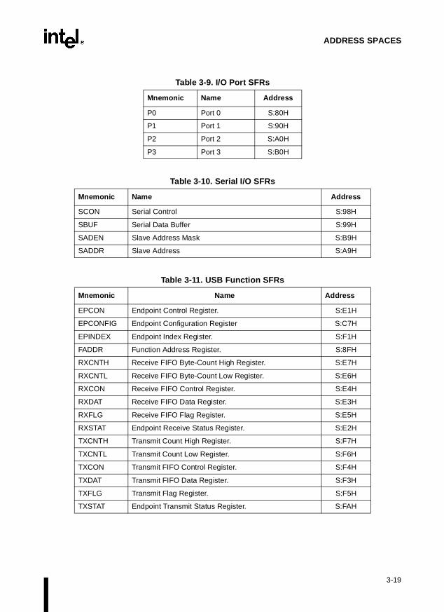
ADDRESS SPACES
Table 3-9. I/O Port SFRs
Mnemonic Name Address
P0 Port 0 S:80H
P1 Port 1 S:90H
P2 Port 2 S:A0H
P3 Port 3 S:B0H
Table 3-10. Serial I/O SFRs
Mnemonic Name Address
SCON Serial Control S:98H
SBUF Serial Data Buffer S:99H
SADEN Slave Address Mask S:B9H
SADDR Slave Address S:A9H
Table 3-11. USB Function SFRs
Mnemonic Name Address
EPCON Endpoint Control Register. S:E1H
EPCONFIG Endpoint Configuration Register S:C7H
EPINDEX Endpoint Index Register. S:F1H
FADDR Function Address Register. S:8FH
RXCNTH Receive FIFO Byte-Count High Register. S:E7H
RXCNTL Receive FIFO Byte-Count Low Register. S:E6H
RXCON Receive FIFO Control Register. S:E4H
RXDAT Receive FIFO Data Register. S:E3H
RXFLG Receive FIFO Flag Register. S:E5H
RXSTAT Endpoint Receive Status Register. S:E2H
TXCNTH Transmit Count High Register. S:F7H
TXCNTL Transmit Count Low Register. S:F6H
TXCON Transmit FIFO Control Register. S:F4H
TXDAT Transmit FIFO Data Register. S:F3H
TXFLG Transmit Flag Register. S:F5H
TXSTAT Endpoint Transmit Status Register. S:FAH
3-19

8x930Ax, 8x930Hx USER’S MANUAL
Table 3-12. USB Hub SFRs
Mnemonic Name Address
HADDR Hub Address Register. S:97H
HPCON Hub Port Control. S:CFH
HPINDEX Hub Port Index Register. S:D4H
HPPWR Hub Port Power Control. S:9AH
HPSC Hub Port Status Change. S:D5H
HPSTAT Hub Port Status. S:D7H
HSTAT Hub Status and Configuration. S:AEH
Table 3-13. Timer/Counter and Watchdog Timer SFRs
Mnemonic Name Address
TL0 Timer/Counter 0 Low Byte S:8AH
TH0 Timer/Counter 0 High Byte S:8CH
TL1 Timer/Counter 1 Low Byte S:8BH
TH1 Timer/Counter 1 High Byte S:8DH
TL2 Timer/Counter 2 Low Byte S:CCH
TH2 Timer/Counter 2 High Byte S:CDH
TCON Timer/Counter 0 and 1 Control S:88H
TMOD Timer/Counter 0 and 1 Mode Control S:89H
T2CON Timer/Counter 2 Control S:C8H
T2MOD Timer/Counter 2 Mode Control S:C9H
RCAP2L Timer 2 Reload/Capture Low Byte S:CAH
RCAP2H Timer 2 Reload/Capture High Byte S:CBH
WDTRST WatchDog Timer Reset S:A6H
3-20

ADDRESS SPACES
Table 3-14. Programmable Counter Array (PCA) SFRs
Mnemonic Name Address
CCON PCA Timer/Counter Control S:D8H
CMOD PCA Timer/Counter Mode S:D9H
CCAPM0 PCA Timer/Counter Mode 0 S:DAH
CCAPM1 PCA Timer/Counter Mode 1 S:DBH
CCAPM2 PCA Timer/Counter Mode 2 S:DCH
CCAPM3 PCA Timer/Counter Mode 3 S:DDH
CCAPM4 PCA Timer/Counter Mode 4 S:DEH
CL PCA Timer/Counter Low Byte S:E9H
CH PCA Timer/Counter High Byte S:F9H
CCAP0L PCA Compare/Capture Module 0 Low Byte S:EAH
CCAP1L PCA Compare/Capture Module 1 Low Byte S:EBH
CCAP2L PCA Compare/Capture Module 2 Low Byte S:ECH
CCAP3L PCA Compare/Capture Module 3 Low Byte S:EDH
CCAP4L PCA Compare/Capture Module 4 Low Byte S:EEH
CCAP0H PCA Compare/Capture Module 0 High Byte S:FAH
CCAP1H PCA Compare/Capture Module 1 High Byte S:FBH
CCAP2H PCA Compare/Capture Module 2 High Byte S:FCH
CCAP3H PCA Compare/Capture Module 3 High Byte S:FDH
CCAP4H PCA Compare/Capture Module 4 High Byte S:FEH
3-21


4Device Configuration


re-
, and
ration
Mem-
d intes
oryomer-
array
4-4.
tion isation
CHAPTER 4DEVICE CONFIGURATION
The 8x930 provides design flexibility by configuring certain operating features during deviceset. These features fall into the following categories:
• external memory interface (page mode, address bits, wait states, range for RD#, WR#PSEN#)
• source mode/binary mode opcodes
• selection of bytes stored on the stack by an interrupt
• mapping of the upper portion of on-chip code memory to region 00:
You can specify a 16-bit, 17-bit, or 18-bit external addresses bus (256 Kbyte external addressspace). Wait state selection provides 0, 1, 2, or 3 wait states.
This chapter provides a detailed discussion of device configuration. It describes the configubytes and provides information to aid you in selecting a suitable configuration for your applica-tion. It discusses the choices involved in configuring the external memory interface and showshow the internal memory space maps into external memory. See “Configuring the External ory Interface” on page 4-7. “Opcode Configurations (SRC)” on page 4-12 discusses the choiceof source mode or binary mode opcode arrangements.
4.1 CONFIGURATION OVERVIEW
The configuration of the 8x930 is established by the reset routine based on information storeconfiguration bytes. The 8x930 stores configuration information in two user configuration by(UCONFIG0 and UCONFIG1) located in code memory. Devices with no on-chip code memfetch configuration data from external memory. Factory programmed ROM devices use custprovided configuration data supplied on floppy disk.
4.2 DEVICE CONFIGURATION
The 8x930 reserves the top eight bytes of the memory address space (FF:FFF8H–FF:FFFFH) foran eight-byte configuration array (Figure 4-1). The two lowest bytes of the configuration are assigned to the two configuration bytes UCONFIG0 (FF:FFF8H) and UCONFIG1(FF:FFF9H). Bit definitions of UCONFIG0 and UCONFIG1 are provided in Figures 4-3 and The upper six bytes of the configuration array are reserved for future use.
When EA# = 1, the 8x930 obtains configuration information at reset from on-chip nonvolatilememory at addresses FF:FFF8H and FF:FFF9H. For ROM devices, configuration informaentered at these addresses during fabrication. The user can verify configuration informstored on-chip using the procedures presented in Chapter 17, “Verifying Nonvolatile Memory.”
4-1

8x930Ax, 8x930Hx USER’S MANUAL
xter-n in anl code
F9H.
For devices without on-chip program memory, configuration information is accessed from enal memory using these same addresses. The designer must store configuration informatioeight-byte configuration array located at the highest addresses implemented in externamemory. See Table 4-1 and Figure 4-2. When EA# = 0, the microcontroller obtains configurationinformation at reset from external memory using internal addresses FF:FFF8H and FF:FF
Figure 4-1. Configuration Array (On-chip)
Table 4-1. External Addresses for Configuration Array
Size of External Address Bus
(Bits)
Address ofConfiguration Array on
External Bus (2)
Address ofConfiguration Byteson External Bus (1)
16 FFF8H–FFFFH UCONFIG1: FFF9H UCONFIG0: FFF8H
17 1FFF8H–1FFFFH UCONFIG1: 1FFF9H UCONFIG0: 1FFF8H
18 3FFF8H–3FFFFH UCONFIG1: 3FFF9H UCONFIG0: 3FFF8H
NOTES:1. When EA# = 0, the reset routine retrieves UCONFIG0 and UCONFIG1 from
external memory using the internal addresses FF:FFF8H and FF:FFF9H which appear on the external address bus (A17, A16, A15:0) as shown in this table. See Figure 4-2.
2. The upper six bytes of the configuration array are reserved for future use.
A4393-01
16-Kbyte Devices
For EA# = 1, configuration information is obtained from the on-chip configuration array located in non-volatile memory at addresses FF:FFF8H - FF:FFFFH.
8-Kbyte Devices
FF:0000H FF:0000H
FF:FFFFH
FF:FFFEH
FF:FFFDH
FF:FFFCH
FF:FFFBH
FF:FFFAH
FF:FFF9H
FF:FFF8H
UCONFIG1
UCONFIG0
Reserved
Detail. On-chip configuration array.
FF:FF:
4-2

DEVICE CONFIGURATION
Figure 4-2. Configuration Array (External)
CAUTIONThe eight highest addresses in the memory address space (FF:FFF8H–FF:FFFFH) are reserved for the configuration array. Do not read or write application code at these locations. These address are also used to access the configuration array in external memory, so the same restrictions apply to the eight highest addresses implemented in external memory. Instructions that might inadvertently cause these addresses to be accessed due to call returns or prefetches should not be located at addresses immediately below the configuration array. Use an EJMP instruction, five or more addresses below the configuration array, to continue execution in other areas of memory.
A4394-01
1FF9H1FF8H
8 Kbytes
3FF9H3FF8H
16 Kbytes
7FF9H7FF8H
32 KbytesFFF9HFFF8H
64 Kbytes
1:FFF9H1:FFF8H
128 Kbytes3:FFF9H
256 Kbytes
3:FFF8Hx:xFFFH
x:xFFEH
x:xFFDH
x:xFFCH
x:xFFBH
x:xFFAH
x:xFF9H
x:xFF8H
UCONFIG1
UCONFIG0
Reserved
This figure shows the addresses of configuration bytes UCONFIG1 and UCONFIG0 in external memory for several memory implementations. For EA# = 0, configuration information is obtained from configuration bytes in external memory using internal addresses FF:FFF8H and FF:FFF9H. In external memory, the eight-byte configuration array is located at the highest addresses implemented.
Detail. Configuration array in external memory.
4-3
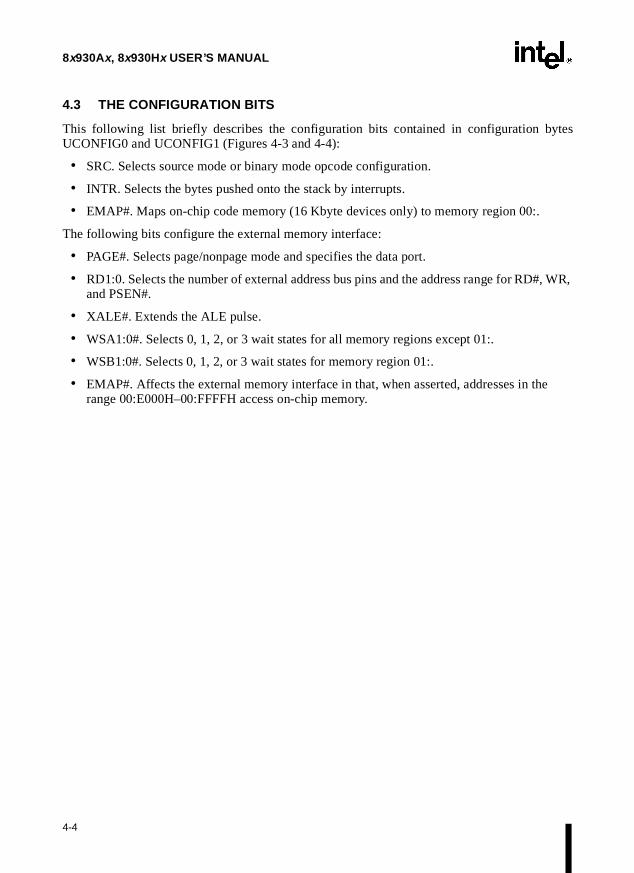
8x930Ax, 8x930Hx USER’S MANUAL
tes
#, WR,
e
4.3 THE CONFIGURATION BITS
This following list briefly describes the configuration bits contained in configuration byUCONFIG0 and UCONFIG1 (Figures 4-3 and 4-4):
• SRC. Selects source mode or binary mode opcode configuration.
• INTR. Selects the bytes pushed onto the stack by interrupts.
• EMAP#. Maps on-chip code memory (16 Kbyte devices only) to memory region 00:.
The following bits configure the external memory interface:
• PAGE#. Selects page/nonpage mode and specifies the data port.
• RD1:0. Selects the number of external address bus pins and the address range for RDand PSEN#.
• XALE#. Extends the ALE pulse.
• WSA1:0#. Selects 0, 1, 2, or 3 wait states for all memory regions except 01:.
• WSB1:0#. Selects 0, 1, 2, or 3 wait states for memory region 01:.
• EMAP#. Affects the external memory interface in that, when asserted, addresses in thrange 00:E000H–00:FFFFH access on-chip memory.
4-4

DEVICE CONFIGURATION
Figure 4-3. User Configuration Byte 0 (UCONFIG0)
UCONFIG0(1), (3)
Address: FF:FFF8H (2)
7 0
— WSA1# WSA0# XALE# RD1 RD0 PAGE# SRC
Bit Number
Bit Mnemonic Function
7 — Reserved:
Reserved for internal or future use. Set this bit when programming UCONFIG0.
6:5 WSA1:0# Wait State A (all regions except 01:):
For external memory accesses, selects the number of wait states for RD#, WR#, and PSEN#.
WSA1# WSA0#0 0 Inserts 3 wait states for all regions except 01: 0 1 Inserts 2 wait states for all regions except 01: 1 0 Inserts 1 wait state for all regions except 01: 1 1 Zero wait states for all regions except 01:
4 XALE# Extend ALE:
Set this bit for ALE = TOSC. Clear this bit for ALE = 3TOSC (adds one external wait state).
3:2 RD1:0 Memory Signal Selection:
RD1:0 bit codes specify an 18-bit, 17-bit, or 16-bit external address bus and address ranges for RD#, WR#, and PSEN#. See Table 4-2 on page 4-7.
1 PAGE# Page Mode Select:
Clear this bit for page mode enabled with A15:8/D7:0 on P2 and A7:0 on P0.Set this bit for page mode disabled with A15:8 on P2 and A7:0/D7:0 on P0.
0 SRC Source Mode/Binary Mode Select:
Set this bit for source mode.Clear this bit for binary mode (opcodes compatible with MCS 51 microcontrollers).
NOTES:1. User configuration bytes UCONFIG0 and UCONFIG1 define the configuration of the 8x930.2. Address. UCONFIG0 is the lowest byte of the 8-byte configuration array. When EA# = 1, the 8x930
fetches configuration information from an on-chip configuration array located in nonvolatile memory at the top of region FF:. When EA# = 0, the 8x930 fetches configuration information from a configuration array located at the highest addresses implemented in external memory using addresses FF:FFF8H and FF:FFF9H. The physical location of the configuration array in external memory depends on the size and decode arrangement of the external memory (Table 4-1 and Figure 4-2).
3. Instructions for verifying on-chip configuration bytes are given in Chapter 17.
4-5
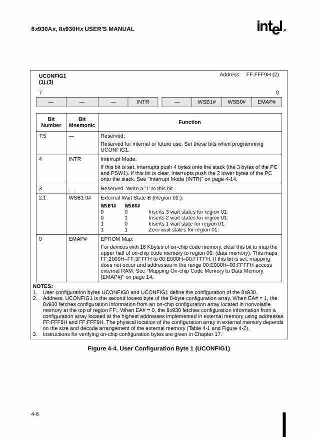
8x930Ax, 8x930Hx USER’S MANUAL
Figure 4-4. User Configuration Byte 1 (UCONFIG1)
UCONFIG1 (1),(3)
Address: FF:FFF9H (2)
7 0
— — — INTR — WSB1# WSB0# EMAP#
Bit Number
Bit Mnemonic Function
7:5 — Reserved:
Reserved for internal or future use. Set these bits when programming UCONFIG1.
4 INTR Interrupt Mode:
If this bit is set, interrupts push 4 bytes onto the stack (the 3 bytes of the PC and PSW1). If this bit is clear, interrupts push the 2 lower bytes of the PC onto the stack. See “Interrupt Mode (INTR)” on page 4-14.
3 — Reserved. Write a ‘1’ to this bit.
2:1 WSB1:0#
External Wait State B (Region 01:):
WSB1# WSB0#0 0 Inserts 3 wait states for region 01: 0 1 Inserts 2 wait states for region 01: 1 0 Inserts 1 wait state for region 01: 1 1 Zero wait states for region 01:
0 EMAP# EPROM Map:
For devices with 16 Kbytes of on-chip code memory, clear this bit to map the upper half of on-chip code memory to region 00: (data memory). This maps FF:2000H–FF:3FFFH to 00:E000H–00:FFFFH. If this bit is set, mapping does not occur and addresses in the range 00:E000H–00:FFFFH access external RAM. See “Mapping On-chip Code Memory to Data Memory (EMAP#)” on page 14.
NOTES:1. User configuration bytes UCONFIG0 and UCONFIG1 define the configuration of the 8x930.2. Address. UCONFIG1 is the second lowest byte of the 8-byte configuration array. When EA# = 1, the
8x930 fetches configuration information from an on-chip configuration array located in nonvolatile memory at the top of region FF:. When EA# = 0, the 8x930 fetches configuration information from a configuration array located at the highest addresses implemented in external memory using addresses FF:FFF8H and FF:FFF9H. The physical location of the configuration array in external memory depends on the size and decode arrangement of the external memory (Table 4-1 and Figure 4-2).
3. Instructions for verifying on-chip configuration bytes are given in Chapter 17.
4-6
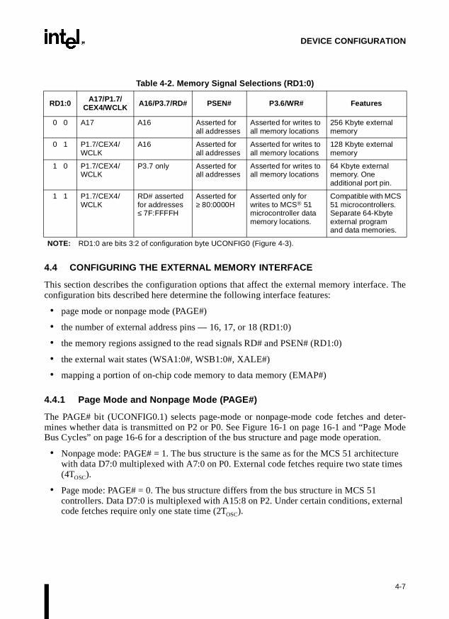
DEVICE CONFIGURATION
. The
deter-
.
cture mes
rnal
4.4 CONFIGURING THE EXTERNAL MEMORY INTERFACE
This section describes the configuration options that affect the external memory interfaceconfiguration bits described here determine the following interface features:
• page mode or nonpage mode (PAGE#)
• the number of external address pins — 16, 17, or 18 (RD1:0)
• the memory regions assigned to the read signals RD# and PSEN# (RD1:0)
• the external wait states (WSA1:0#, WSB1:0#, XALE#)
• mapping a portion of on-chip code memory to data memory (EMAP#)
4.4.1 Page Mode and Nonpage Mode (PAGE#)
The PAGE# bit (UCONFIG0.1) selects page-mode or nonpage-mode code fetches andmines whether data is transmitted on P2 or P0. See Figure 16-1 on page 16-1 and “Page ModeBus Cycles” on page 16-6 for a description of the bus structure and page mode operation
• Nonpage mode: PAGE# = 1. The bus structure is the same as for the MCS 51 architewith data D7:0 multiplexed with A7:0 on P0. External code fetches require two state ti(4TOSC).
• Page mode: PAGE# = 0. The bus structure differs from the bus structure in MCS 51 controllers. Data D7:0 is multiplexed with A15:8 on P2. Under certain conditions, extecode fetches require only one state time (2TOSC).
Table 4-2. Memory Signal Selections (RD1:0)
RD1:0 A17/P1.7/CEX4/WCLK A16/P3.7/RD# PSEN# P3.6/WR# Features
0 0 A17 A16 Asserted for all addresses
Asserted for writes to all memory locations
256 Kbyte external memory
0 1 P1.7/CEX4/ WCLK
A16 Asserted for all addresses
Asserted for writes to all memory locations
128 Kbyte external memory
1 0 P1.7/CEX4/ WCLK
P3.7 only Asserted for all addresses
Asserted for writes to all memory locations
64 Kbyte external memory. One additional port pin.
1 1 P1.7/CEX4/ WCLK
RD# asserted for addresses≤ 7F:FFFFH
Asserted for ≥ 80:0000H
Asserted only for writes to MCS® 51 microcontroller data memory locations.
Compatible with MCS 51 microcontrollers. Separate 64-Kbyte external program and data memories.
NOTE: RD1:0 are bits 3:2 of configuration byte UCONFIG0 (Figure 4-3).
4-7

8x930Ax, 8x930Hx USER’S MANUAL
esl WR#.
Chap-
4.4.2 Configuration Bits RD1:0
The RD1:0 configuration bits (UCONFIG0.3:2) determine the number of external address linand the address ranges for asserting the read signals PSEN#/RD# and the write signaThese selections offer different ways of addressing external memory. Figures 4-5 and 4-6 showhow internal memory space maps into external memory space for the four values of RD1:0.ter 16, “External Memory Interface,” provides examples of external memory designs for eachchoice of RD1:0.
Figure 4-5. Internal/External Address Mapping (RD1:0 = 00 and 01)
FF:
01:
PSEN#, WR#
PSEN#, WR#
A4218-02
FF:
FE:
01:
00:
RD1:0 = 00
18 external address bits: P0, P2, A16, A17
PSEN#, WR#
PSEN#, WR#
01:, FF:
00:, FE:
01
FF:
FE:
00
256 Kbytes
128 Kbytes
Notes: 1. Maximum external memory 2. Single read signal
Note: Single read signal
Internal Memory with Read/Write Signals
External Memory
A16
1
0
RD1:0 = 01
A17:16
1 1
1 0
0 1
0 0
Internal Memory with Read/Write Signals
External Memory
17 external address bits: P0, P2, A16
FE:
00:
4-8

DEVICE CONFIGURATION
Figure 4-6. Internal/External Address Mapping (RD1:0 = 10 and 11)
FF:
01:
PSEN#
RD#, WR#
A4217-02
FF:
FE:
01:
00:
RD1:0 = 10
16 external address bits: P0, P2
PSEN#, WR#
PSEN#, WR#
FE:, FF:
00:, 01:
00:, 01:, FE:, FF:
64 Kbytes
128 Kbytes
Notes: 1. Single read signal 2. P3.7/RD#/A16 functions only as P3.7
Note: 1. Compatible with MCS® 51 microcontrollers 2. Cannot write to regions FC:–FF:
Internal Memory with Read/Write Signals
External Memory
RD1:0 = 11
Internal Memory with Read/Write Signals
External Memory
16 external address bits: P0, P2
FE:
00:
4-9

8x930Ax, 8x930Hx USER’S MANUAL
xternalresss thatxternal
00H
p into
doesguredcesses
ing lo-Bus,
(from4 thel Flash
d A16al ofto the FF:.
f pinun-em-
Kbyte-17 is pins
A key to the memory interface is the relationship between internal memory addresses and ememory addresses. While the 8x930 has 24 internal address bits, the number of external addlines is less than 24 (i.e., 16, 17, or 18, depending on the values of RD1:0). This meanreads/writes to different internal memory addresses can access the same location in ememory.
For example, if the 8x930 is configured for 18 external address lines, a write to location 01:60and a write to location FF:6000H accesses the same 18-bit external address (1:6000H) becauseA16 = 1 and A17 = 1 for both internal addresses. In other words, regions 00: and FE: mathe same 64 Kbyte region in external memory.
In some situations, however, a multiple mapping from internal memory to external memorynot preclude using more than one region. For example, for a device with on-chip ROM confifor 17 address bits and with EA# = 1, an access to FF:0000H–FF:3FFFH (16 Kbytes) acthe on-chip ROM, while an access to 01:0000H–01:3FFFH is to external memory. In this case,you could execute code from these locations in region FF: and store data in the correspondcations in region 01: without conflict. See Figure 4-5 and “Example 1: RD1:0 = 00, 18-bit External Flash and RAM” on page 16-17.”
4.4.2.1 RD1:0 = 00 (18 External Address Bits)
The selection RD1:0 = 00 provides 18 external address bits: A15:0 (ports P0 and P2), A16P3.7/RD#/A16), and A17 (from P1.7/CEX4/A17/WCLK). Bits A16 and A17 can select four 6Kbyte regions of external memory for a total of 256 Kbytes (top half of Figure 4-5). This islargest possible external memory space. See “Example 1: RD1:0 = 00, 18-bit Bus, Externaand RAM” on page 16-17.
4.4.2.2 RD1:0 = 01 (17 External Address Bits)
The selection RD1:0 = 01 provides 17 external address bits: A15:0 (ports P0 and P2) an(from P3.7/RD#/A16). Bit A16 can select two 64 Kbyte regions of external memory for a tot128 Kbytes (bottom half of Figure 4-5). Regions 00: and FE: (each having A16 = 0) map insame 64 Kbyte region in external memory. This duplication also occurs for regions 01: and
This selection provides a 128 Kbyte external address space. The advantage of this selection, incomparison with the 256 Kbyte external memory space with RD1:0 = 00, is the availability oP1.7/CEX4/A17/WCLK for general I/O, PCA I/O or real-time wait clock output. I/O P3.7 is available. All four 64 Kbyte regions are stored by PSEN# and WR#. Chapter 16, “External Mory Interface,” shows examples of memory designs with this option.
4.4.2.3 RD1:0 = 10 (16 External Address Bits)
For RD1:0 = 10, the 16 external address bits (A15:0 on ports P0 and P2) provide a single 64region in external memory (top of Figure 4-6). This selection provides the smallest external memory space; however, pin P3.7/RD#/A16 is available for general I/O and pin P1.7/CEX4/Aavailable for general I/O or PCA I/O. This selection is useful when the availability of theseis required and/or a small amount of external memory is sufficient.
4-10

DEVICE CONFIGURATION
d P2).gions
ection
a
be ad-arizess, see
ed by:. Theby 1,
page
4.4.2.4 RD1:0 = 11 (Compatible with MCS 51 Microcontrollers)
The selection RD1:0 = 11 provides only 16 external address bits (A15:0 on ports P0 anHowever, PSEN# is the read signal for regions FE:–FF:, while RD# is the read signal for re00:–01: (bottom of Figure 4-6). The two read signals effectively expand the external memoryspace to two 64 Kbyte regions. WR# is asserted only for writes to regions 00:–01:. This selprovides compatibility with MCS 51 microcontrollers, which have separate external memoryspaces for code and data.
4.4.3 Wait State Configuration Bits
You can add wait states to external bus cycles by extending the RD#/WR#/PSEN# pulse nd/orextending the ALE pulse. Each additional wait state extends the pulse by 2TOSC. A separate waitstate specification for external accesses via region 01: permits a slow external device to dressed in region 01: without slowing accesses to other external devices. Table 4-3 summthe wait state selections for RD#,WR#,PSEN#. For waveform diagrams showing wait state“External Bus Cycles With Configurable Wait States” on page 16-8.
4.4.3.1 Configuration Bits WSA1:0 #, WSB1:0#
The WSA1:0# wait state bits (UCONFIG0.6:5) permit RD#, WR#, and PSEN# to be extend1, 2, or 3 wait states for accesses to external memory via all regions except region 01WSB1:0# wait state bits (UCONFIG1.2:1) permit RD#, WR#, and PSEN# to be extended 2, or 3 wait states for accesses to external memory via region 01:.
4.4.3.2 Configuration Bit XALE#
Clearing XALE# (UCONFIG0.4) extends the time ALE is asserted from TOSC to 3TOSC. This ac-commodates an address latch that is too slow for the normal ALE signal. Figure 16-10 on16-10 shows an external bus cycle with ALE extended.
Table 4-3. RD#, WR#, PSEN# External Wait States
8x930
Regions00: FE: FF:
WSA1# WSA0#0 00 11 01 1
3 Wait States2 Wait States1 Wait State0 Wait States
Region 01: WSB1# WSB0#0 00 11 01 1
3 Wait States2 Wait States1 Wait State0 Wait States
4-11

8x930Ax, 8x930Hx USER’S MANUAL
de ar-
t SRC-
ford. De-
ting the
inctionsserved
prefix
(com-scape
shows
etter
ill be
od-g thehitec-
4.5 OPCODE CONFIGURATIONS (SRC)
The SRC configuration bit (UCONFIG0.0) selects the source mode or binary mode opcorangement. Opcodes for the 8x930 architecture are listed in Table A-6 on page A-4 and Table A-7on page A-5. Note that in Table A-6 every opcode (00H–FFH), is used for an instruction excepA5H (ESC), which provides an alternative set of opcodes for columns 6H through FH. Thebit selects which set of opcodes is assigned to columns 6H through FH and which set is the alternative.
Binary mode and source mode refer to two ways of assigning opcodes to the instruction setthe 8x930 architecture. One of these modes must be selected when the chip is configurepending on the application, binary mode or source mode may produce more efficient code. Thissection describes the binary and source modes and provides some guidelines for selecmode for your application.
The 8x930 architecture has two types of instructions:
• instructions that originate in the MCS® 51 architecture
• instructions that are common with the MCS® 251 architecture
Figure 4-7 shows the opcode map for binary mode. Area I (columns 1 through 5 in Table A-7)and area II (columns 6 through F) make up the opcode map for the instructions that originatethe MCS 51 architecture. Area III in Figure 4-7 represents the opcode map for the instruthat are common with the MCS 251 architecture (Table A-7). Some of these opcodes are refor future instructions. Note that the opcode values for areas II and III are identical (06H–FFH).To distinguish between the two areas in binary mode, the opcodes in area III are given theA5H. The area III opcodes are thus A506H–A5FFH.
Figure 4-8 shows the opcode map for source mode. Areas II and III have switched placespare with Figure 4-7). In source mode, opcodes for instructions in area II require the A5F eprefix while opcodes for instructions in area III do not.
To illustrate the difference between the binary-mode and source-mode opcodes, Table 4-4the opcode assignments for three sample instructions.
4.5.1 Selecting Binary Mode or Source Mode
If a system was originally developed using an MCS 51 microcontroller, and if the new 8x930-based system will run code written for the MCS 51 microcontroller, performance will be bwith the 8x930 running in binary mode. Object code written for the MCS 51 microcontroller runsfaster on the 8x930.
However, if most of the code is rewritten using the MCS 251 instruction set, performance wbetter with the 8x930 running in source mode. In this case, the 8x930 can run significantly fasterthan the MCS 51 microcontroller.
If you have code that was written for an MCS 51 microcontroller and you want to run it unmified on an 8x930, choose binary mode. You can use the object code without reassemblinsource code. You can also assemble the source code with an assembler for the MCS 251 arcture and have it produce object code that is binary-compatible with MCS 51 microcontrollers.
4-12

DEVICE CONFIGURATION
Figure 4-7. Binary Mode Opcode Map
Figure 4-8. Source Mode Opcode Map
A4131-01
I II
0H 5H FH6H0H
FH
MCS® 51 Architecture
MCS 51 Architecture
III
6H FH0H
FH
MCS 251 Architecture
A5H Prefix
A4130-01
I III
0H 5H FH6H0H
FH
MCS® 51 Architecture
MCS 251 Architecture
II
6H FH0H
FH
MCS 51 Architecture
A5H Prefix
4-13

8x930Ax, 8x930Hx USER’S MANUAL
moreinstruc-
e stor-ed by
idess codeOn-chipng to
rrupt
wingd uses
k in thebytesddress
If a program uses only instructions from the MCS 51 architecture, the binary-mode code isefficient because it uses no prefixes. On the other hand, if a program uses many more new tions than instructions from the MCS 51 architecture, source mode is likely to produce more ef-ficient code. For a program where the choice is not clear, the better mode can be found byexperimenting with a simulator.
For both architectures, an instruction with a prefixed opcode requires one more byte for codage, and if an additional fetch is required for the extra byte, the execution time is increasone state. This means that using fewer prefixed opcodes produces more efficient code.
4.6 MAPPING ON-CHIP CODE MEMORY TO DATA MEMORY (EMAP#)
For devices with 16 Kbytes of on-chip code memory, the EMAP# bit (UCONFIG1.0) provthe option of accessing the upper half of on-chip code memory as data memory. This allowconstants to be accessed as data in region 00: using direct addressing. See “Accessing Code Memory in Region 00:” on page 3-9 for the exact conditions required for this mappibe effective.
EMAP# = 0. For the 83930AE and 83930HE, the upper eight Kbytes of on-chip code memory(FF:2000–FF:3FFFH are mapped to locations 00:E000H–00:FFFFH.
EMAP# = 1. Mapping of on-chip code memory to region 00: does not occur. Addresses in therange 00:E000H–00:FFFFH access external RAM.
4.7 INTERRUPT MODE (INTR)
The INTR bit (UCONFIG1.4) determines what bytes are stored on the stack when an inteoccurs and how the RETI (Return from Interrupt) instruction restores operation.
For INTR = 0, an interrupt pushes the two lower bytes of the PC onto the stack in the folloorder: PC.7:0, PC.15:8. The RETI instruction pops these two bytes in the reverse order anthem as the 16-bit return address in region FF:.
For INTR = 1, an interrupt pushes the three PC bytes and the PSW1 register onto the stacfollowing order: PSW1, PC.23:16, PC.7:0, PC.15:8. The RETI instruction pops these four and then returns to the specified 24-bit address, which can be anywhere in the 16 Mbyte aspace.
Table 4-4. Examples of Opcodes in Binary and Source Modes
InstructionOpcode
Binary Mode Source Mode
DEC A 14H 14H
SUBB A,R4 9CH A59CH
SUB R4,R4 A59CH 9CH
4-14

5Programming Considerations


the in-. Theon Set
seticientonfigu- “Op-
thet for, 16-cess-gram-
ions.; bit in-
(doubler-byte
in
CHAPTER 5PROGRAMMING CONSIDERATIONS
The instruction set for the architecture supports the instruction set for the MCS® 51 architectureand MCS® 251 architecture. This chapter describes the addressing modes and summarizesstruction set, which is divided into data instructions, bit instructions, and control instructionsprogram status word registers PSW and PSW1 are also described. Appendix A, “InstructiReference,” contains an opcode map and a detailed description of each instruction.
NOTEThe instruction execution times given in Appendix A are for code executing from external memory and for data that is read from and written to on-chip RAM. Execution times are increased by accessing peripheral SFRs, accessing data in external memory, using a wait state, or extending the ALE pulse.
For some instructions, accessing the port SFRs (Px, x = 3:0) increases the execution time. These cases are noted in the tables in Appendix A.
5.1 SOURCE MODE OR BINARY MODE OPCODES
Source mode and Binary mode refer to the two ways of assigning opcodes to the instructionof the 8x930. Depending on the application, one mode or the other may produce more effcode. The mode is established during device reset based on the value of the SRC bit in cration byte UCONFIG0. For information regarding the selection of the opcode mode, seecode Configurations (SRC)” on page 4-12.
5.2 PROGRAMMING FEATURES OF THE 8x930 ARCHITECTURE
The instruction set for 8x930 microcontrollers provides the user with instructions that exploit features of the MCS 251 architecture while maintaining compatibility with the instruction seMCS 51 microcontrollers. Many of the MCS 251 architecture instructions operate on 8-bitbit, or 32-bit operands. (In comparison with 8-bit and 16-bit operands, 32-bit operands are aced with fewer addressing modes.) This capability increases the ease and efficiency of proming the 8x930 microcontroller in a high-level language such as C.
The instruction set is divided into data instructions, bit instructions, and control instructThese are described in this chapter. Data instructions process 8-bit, 16-bit, and 32-bit datastructions manipulate bits; and control instructions manage program flow.
5.2.1 Data Types
Table 5-1 lists the data types that are addressed by the instruction set. Words or dwords words) can be in stored memory starting at any byte address; alignment on two-byte or fouboundaries is not required. Words and dwords are stored in memory and the register filebigendien form.
5-1

8x930Ax, 8x930Hx USER’S MANUAL
nf the
. Wile, theon of illus-
in that1, ...,1, ...,s.
index
iguretween:0ction.
5.2.1.1 Order of Byte Storage for Words and Double Words
The 8x930 microcontroller stores words (2 bytes) and double words (4 bytes) in memory and ithe register file in big endien form. In memory storage, the most significant byte (MSB) oword or double word is stored in the memory byte specified in the instruction; the remaining bytesare stored at higher addresses, with the least significant byte (LSB) at the highest addressordsand double words can be stored in memory starting at any byte address. In the register fMSB is stored in the lowest byte of the register specified in the instruction. For a descriptithe register file, see “8x930 Register File” on page 3-9. The code fragment in Figure 5-1trates the storage of words and double words in big endien form.
5.2.2 Register Notation
In register-addressing instructions, specific indices denote the registers that can be usedinstruction. For example, the instruction ADD A,Rn uses “Rn” to denote any one of R0, RR7; i.e., the range of n is 0–7. The instruction ADD Rm,#data uses “Rm” to denote R0, RR15; i.e., the range of m is 0–15. Table 5-2 summarizes the notation used for the register indiceWhen an instruction contains two registers of the same type (e.g., MOV Rmd,Rms) the first“d” denotes “destination” and the second index “s” denotes “source.”
5.2.3 Address Notation
In the 8x930 architecture, memory addresses include a region number (00:, 01:, ..., FF:) (F3-5 on page 3-7). SFR addresses have a prefix “S:” (S:000H–S:1FFH). The distinction bememory addresses and SFR addresses is necessary because memory locations 00000H–00:01FFH and SFR locations S:000H–S:1FFH can both be directly addressed in an instru
Table 5-1. Data Types
Data Type Number of Bits
Bit 1
Byte 8
Word 16
Dword (Double Word) 32
5-2

PROGRAMMING CONSIDERATIONS
ationsare ad-
for
d thed
Figure 5-1. Word and Double-word Storage in Big Endien Form
Instructions in the MCS 51 architecture use 80H–FFH as addresses for both memory locand SFRs, because memory locations are addressed only indirectly and SFR locations dressed only directly. For compatibility, firmware tools for 8x930 microcontrollers recognize thisnotation for instructions in the 8x930 architecture. No change is necessary in any code writtenMCS 51 controllers.
For the MCS 251 architecture instructions, the memory region prefixes (00:, 01, ..., FF:) anSFR prefix (S:) are required. Also, firmware tools for the 8x930 architecture permit 00: to be usefor memory addresses 00H–FFH and permit the prefix S: to be used for SFR addresses in instruc-tions in the 8x930 architecture.
Table 5-2. Notation for Byte Registers, Word Registers, and Dword Registers
Register Type
RegisterSymbol
DestinationRegister
SourceRegister Register Range
Byte
Ri — — R0, R1
Rn — — R0–R7
Rm Rmd Rms R0–R15
Word WRj WRjd WRjs WR0, WR2, WR4, ..., WR30
Dword DRk DRkd DRks DR0, DR4, DR8, ..., DR28, DR56, DR60
MOV WR0,#A3B6H MOV 00:0201H,WR0 MOV DR4,#0000C4D7H
A3H B6H
2 3
WR0
4 5 60 1 7
00H 00H C4H D7H
DR4
Register File
Memory
Contents of register file and memory after execution
A4242-01
200H 201H 202H 203H
A3H B6H
5-3

8x930Ax, 8x930Hx USER’S MANUAL
d
to
s” on
, andions.
ble 5-4struc-
5.2.4 Addressing Modes
The 8x930 architecture supports the following addressing modes:
• register addressing: The instruction specifies the register that contains the operand.
• immediate addressing: The instruction contains the operand.
• direct addressing: The instruction contains the operand address.
• indirect addressing: The instruction specifies the register that contains the operand address.
• displacement addressing: The instruction specifies a register and an offset. The operanaddress is the sum of the register contents (the base address) and the offset.
• relative addressing: The instruction contains the signed offset from the next instructionthe target address (the address for transfer of control, e.g., the jump address).
• bit addressing: The instruction contains the bit address.
More detailed descriptions of the addressing modes are given in “Data Addressing Modepage 5-4, “Bit Addressing” on page 5-10, and “Addressing Modes for Control Instructions” onpage 5-12.
5.3 DATA INSTRUCTIONS
Data instructions consist of arithmetic, logical, and data-transfer instructions for 8-bit, 16-bit32-bit data. This section describes the data addressing modes and the set of data instruct
5.3.1 Data Addressing Modes
This section describes the data-addressing modes, which are summarized in two tables: Tafor the instructions that are native to the MCS 51 architecture, and Table 5-4 for the data intions in the MCS 251architecture.
NOTEReferences to registers R0–R7, WR0–WR6, DR0, and DR2 always refer to the register bank that is currently selected by the PSW and PSW1 registers (see “Program Status Words” on page 5-15). Registers in all banks (active and inactive) can be accessed as memory locations in the range 00H–1FH.
Instructions from the MCS 51 architecture access external memory through the region of memory specified by byte DPXL in the extended data pointer register, DPX (DR56). Following reset, DPXL contains 01H, which maps the external memory to region 01:. You can specify a different region by writing to DR56 or the DPXL SFR (see “Dedicated Registers” on page 3-12).
5-4

PROGRAMMING CONSIDERATIONS
uction
data 16-bit ord,
4) that
) as FRs
in
=
5.3.1.1 Register Addressing
Both architectures address registers directly:
• MCS 251 architecture. In the register addressing mode, the operand(s) in a data instrare in byte registers (R0–R15), word registers (WR0, WR2, ..., WR30), or dword registers(DR0, DR4, ..., DR28, DR56, DR60).
• MCS 51 architecture. Instructions address registers R0–R7 only.
5.3.1.2 Immediate
Both architectures use immediate addressing.
• MCS 251 architecture. In the immediate addressing mode, the instruction contains theoperand itself. Byte operations use 8-bit immediate data (#data); word operations use immediate data (#data16). Dword operations use 16-bit immediate data in the lower wand either zeros in the upper word (denoted by #0data16), or ones in the upper word (denoted by #1data16). MOV instructions that place 16-bit immediate data into a dword register (DRk), place the data either into the upper word while leaving the lower word unchanged, or into the lower word with a sign extension or a zero extension.The increment and decrement instructions contain immediate data (#short = 1, 2, or specifies the amount of the increment/decrement.
• MCS 51 architecture. Instructions use only 8-bit immediate data (#data).
5.3.1.3 Direct
• MCS 251 architecture. In the direct addressing mode, the instruction contains the address of the data operand. The 8-bit direct mode addresses on-chip RAM (dir8 = 00:0000H–00:007FH) as both bytes and words, and addresses the SFRs (dir8 = S:080H–S:1FFHbytes only. (See the second note in “Data Addressing Modes” on page 5-4 regarding Sin the MCS 251 architecture.) The 16-bit direct mode addresses both bytes and wordsmemory (dir16 = 00:0000H–00:FFFFH).
• MCS 51 architecture. The 8-bit direct mode addresses 256 bytes of on-chip RAM (dir800H–7FH) as bytes only and the SFRs (dir8 = 80H–FFH) as bytes only.
Table 5-3. Addressing Modes for Data Instructions in the MCS ® 51 Architecture
Mode Address Range of Operand
Assembly Language Reference Comments
Register 00H–1FH R0–R7(Bank selected by PSW)
Immediate Operand in Instruction #data = #00H–#FFH
Direct
00H–7FH dir8 = 00H–7FH On-chip RAM
SFRs dir8 = 80H–FFHor SFR mnemonic. SFR address
5-5

8x930Ax, 8x930Hx USER’S MANUAL
ways aaddress
can . (If k
e in the
ory
to
5.3.1.4 Indirect
In arithmetic and logical instructions that use indirect addressing, the source operand is albyte, and the destination is either the accumulator or a byte register (R0–R15). The source is a byte, word, or dword. The two architectures do indirect addressing via different registers:
• MCS 251 architecture. Memory is indirectly addressed via word and dword registers:
— Word register (@WRj, j = 0, 2, 4, ..., 30). The 16-bit address in WRj can access locations 00:0000H–00:FFFFH.
— Dword register (@DRk, k = 0, 4, 8, ..., 28, 56, and 60). The 24 least significant bitsaccess the entire 16-Mbyte address space. The upper eight bits of DRk must be 0you use DR60 as a general data pointer, be aware that DR60 is the extended stacpointer register SPX.)
• MCS 51 architecture. Instructions use indirect addressing to access on-chip RAM, codmemory, and external data RAM. (See the second note in “Data Addressing Modes” onpage 5-4 regarding the region of external data RAM that is addressed by instructions MCS 51 architecture.)
— Byte register (@Ri, i = 1, 2). Registers R0 and R1 indirectly address on-chip memlocations 00H–FFH and the lowest 256 bytes of external data RAM.
— 16-bit data pointer (@DPTR or @A+DPTR). The MOVC and MOVX instructions use these indirect modes to access code memory and external data RAM.
— 16-bit program counter (@A+PC). The MOVC instruction uses this indirect mode access code memory.
Indirect
00H–FFH @R0, @R1Accesses on-chip RAM or the lowest 256 bytes of external data memory (MOVX).
0000H–FFFFH @DPTR, @A+DPTR Accesses external data memory (MOVX).
0000H–FFFFH @A+DPTR, @A+PC Accesses region FF: of code memory (MOVC).
Table 5-3. Addressing Modes for Data Instructions in the MCS ® 51 Architecture (Continued)
Mode Address Range of Operand
Assembly Language Reference Comments
5-6

PROGRAMMING CONSIDERATIONS
Table 5-4. Addressing Modes for Data Instructions in the MCS ® 251 Architecture
Mode Address Range of Operand
Assembly Language Notation Comments
Register00:0000H–00:001FH
(R0–R7, WR0–WR3, DR0, DR2) (1)
R0–R15, WR0–WR30,DR0–DR28, DR56, DR60
R0–R7, WR0–WR6, DR0, and DR2 are in the register bank currently selected by the PSW and PSW1.
Immediate,2 bits
N.A. (Operand is in theinstruction) #short = 1, 2, or 4 Used only in increment and
decrement instructions.
Immediate,8 bits
N.A. (Operand is in theinstruction) #data8 = #00H–#FFH
Immediate,16 bits
N.A. (Operand is in theinstruction) #data16 = #0000H–#FFFFH
Direct, 8 address bits
00:0000H–00:007FH dir8 = 00:0000H–00:007FH On-chip RAM
SFRs dir8 = S:080H–S:1FFH (2)or SFR mnemonic SFR address
Direct,16 address bits 00:0000H–00:FFFFH dir16 = 00:0000H–00:FFFFH
Indirect,16 address bits 00:0000H–00:FFFFH @WR0–@WR30
Indirect, 24 address bits 00:0000H–FF:FFFFH @DR0–@DR30, @DR56,
@DR60Upper 8 bits of DRk must be 00H.
Displacement,16 address bits 00:0000H–00:FFFFH
@WRj + dis16 =
@WR0 + 0H through@WR30 + FFFFH
Offset is signed; address wraps around in region 00:.
Displacement,24 address bits 00:0000H–FF:FFFFH
@DRk + dis24 =
@DR0 + 0H through@DR28 + FFFFH,
@DR56 + (0H–FFFFH),@DR60 + (0H–FFFFH)
Offset is signed, upper 8 bits of DRk must be 00H.
NOTES:1. These registers are accessible in the memory space as well as in the register file (see “8x930
Register File” on page 3-9).2. The MCS 251 architecture supports SFRs in locations S:000H–S:1FFH; however, in the 8x930 all
SFRs are in the range S:080H–S:0FFH.
5-7

8x930Ax, 8x930Hx USER’S MANUAL
urce tolowestntainsm are exceedscomese com-
byte0. The
D and in
ol-
e dif-uent use
e in- byte,rt).
ed user
5.3.1.5 Displacement
Several move instructions use displacement addressing to move bytes or words from a soa destination. Sixteen-bit displacement addressing (@WRj+dis16) accesses indirectly the 64 Kbytes in memory. The base address can be in any word register WRj. The instruction coa 16-bit signed offset which is added to the base address. Only the lowest 16 bits of the suused to compute the operand address. If the sum of the base address and a positive offsetFFFFH, the computed address wraps around within region 00: (e.g. F000H + 2005H be1005H). Similarly, if the sum of the base address and a negative offset is less than zero, thputed address wraps around the top of region 00: (e.g., 2005H + F000H becomes 1005H).
Twenty-four-bit displacement addressing (@DRk+dis24) accesses indirectly the entire 16-Maddress space. The base address must be in DR0, DR4, ..., DR24, DR28, DR56, or DR6upper byte in the dword register must be zero. The instruction contains a 16-bit signed offsetwhich is added to the base address.
5.3.2 Arithmetic Instructions
The set of arithmetic instructions is greatly expanded in the MCS 251 architecture. The ADSUB instructions (Table A-19 on page A-13) operate on byte and word data that is accessedseveral ways:
• as the contents of the accumulator, a byte register (Rn), or a word register (WRj)
• in the instruction itself (immediate data)
• in memory via direct or indirect addressing
The ADDC and SUBB instructions (Table A-19) are the same as those for MCS 51 microcontrlers.
The CMP (compare) instruction (Table A-20 on page A-14) calculates the difference of two bytesor words and then writes to flags CY, OV, AC, N, and Z in the PSW and PSW1 registers. Thference is not stored. The operands can be addressed in a variety of modes. The most freqof CMP is to compare data or addresses preceding a conditional jump instruction.
Table A-21 on page A-14 lists the INC (increment) and DEC (decrement) instructions. Thstructions for MCS 51 microcontrollers are supplemented by instructions that can addressword, and dword registers and increment or decrement them by 1, 2, or 4 (denoted by #shoThese instructions are supplied primarily for register-based address pointers and loop counters.
The 8x930 architecture provides the MUL (multiply) and DIV (divide) instructions for unsign8-bit and 16-bit data (Table A-22 on page A-15). Signed multiply and divide are left for theto manage through a conversion process. The following operations are implemented:
• eight-bit multiplication: 8 bits × 8 bits → 16 bits
• sixteen-bit multiplication: 16 bits × 16 bits → 32 bits
• eight-bit division: 8 bits ÷ 8 bits → 16 bits (8-bit quotient, 8-bit remainder)
• sixteen-bit division: 16 bits ÷ 16 bits → 32 bits (16-bit quotient, 16-bit remainder)
5-8

PROGRAMMING CONSIDERATIONS
js), or
stored isi-gless.
NL, on
mme-and N
s that
se in-h, and
in the
PXL,
ccu-
ntsn bit
These instructions operate on pairs of byte registers (Rmd,Rms), word registers (WRjd,WRthe accumulator and B register (A,B). For 8-bit register multiplies, the result is stored in thewordregister that contains the first operand register. For example, the product from an instructionMUL R3,R8 is stored in WR2. Similarly, for 16-bit multiplies, the result is stored in the dwordregister that contains the first operand register. For example, the product from the instructionMUL WR6,WR18 is stored in DR4.
For 8-bit divides, the operands are byte registers. The result is stored in the word register that con-tains the first operand register. The quotient is stored in the lower byte, and the remainder isin the higher byte. A 16-bit divide is similar. The first operand is a word register, and the resultstored in the double word register that contains that word register. If the second operand (the dvisor) is zero, the overflow flag (OV) is set and the other bits in PSW and PSW1 are meanin
5.3.3 Logical Instructions
The 8x930 architecture provides a set of instructions that perform logical operations. The AORL, and XRL (logical AND, logical OR, and logical exclusive OR) instructions operatebytes and words that are accessed via several addressing modes (Table A-23 on page A-16). Abyte register, word register, or the accumulator can be logically combined with a register, idiate data, or data that is addressed directly or indirectly. These instructions affect the Z flags.
In addition to the CLR (clear), CPL (complement), SWAP (swap), and four rotate instructionoperate on the accumulator, 8x930 microcontroller has three shift commands for byte and wordregisters:
• SLL (Shift Left Logical) shifts the register one bit left and replaces the LSB with 0
• SRL (Shift Right Logical) shifts the register one bit right and replaces the MSB with 0
• SRA (Shift Right Arithmetic) shifts the register one bit right; the MSB is unchanged
5.3.4 Data Transfer Instructions
Data transfer instructions copy data from one register or memory location to another. Thestructions include the move instructions (Table A-24 on page A-18) and the exchange, puspop instructions (Table A-25 on page A-21). Instructions that move only a single bit are listedwith the other bit instructions in Table A-26 on page A-22.
MOV (Move) is the most versatile instruction, and its addressing modes are expanded 8x930 architecture. MOV can transfer a byte, word, or dword between any two registers or be-tween a register and any location in the address space.
The MOVX (Move External) instruction moves a byte from external memory to the accumulatoror from the accumulator to memory. The external memory is in the region specified by Dwhose reset value is 01H (see “Dedicated Registers” on page 3-12).
The MOVC (Move Code) instruction moves a byte from code memory (region FF:) to the amulator.
MOVS (Move with Sign Extension) and MOVZ (Move with Zero Extension) move the conteof an 8-bit register to the lower byte of a 16-bit register. The upper byte is filled with the sig
5-9

8x930Ax, 8x930Hx USER’S MANUAL
di-
ter orf theary
ng it imme-
o a reg-
gories
bit
a.
bed
5-5). of bits
bits. Inithin
ion with-
(MOVS) or zeros (MOVZ). The MOVH (Move to High Word) instruction places 16-bit immeate data into the high word of a dword register.
The XCH (Exchange) instruction interchanges the contents of the accumulator with a regismemory location. The XCHD (Exchange Digit) instruction interchanges the lower nibble oaccumulator with the lower nibble of a byte in on-chip RAM. XCHD is useful for BCD (bincoded decimal) operations.
The PUSH and POP instructions facilitate storing information (PUSH) and then retrievi(POP) in reverse order. Push can push a byte, a word, or a dword onto the stack, using thediate, direct, or register addressing modes. POP can pop a byte or a word from the stack tister or to memory.
5.4 BIT INSTRUCTIONS
A bit instruction addresses a specific bit in a memory location or SFR. There are four cateof bit instructions:
• SETB (Set Bit), CLR (Clear Bit), CPL (Complement Bit). These instructions can set, clear or complement any addressable bit.
• ANL (And Logical), ANL/ (And Logical Complement), ORL (OR Logical), ORL/ (Or Logical Complement). These instructions allow ANDing and ORing of any addressable or its complement with the CY flag.
• MOV (Move) instructions transfer any addressable bit to the carry (CY) bit or vice vers
• Bit-conditional jump instructions execute a jump if the bit has a specified state. The bit-conditional jump instructions are classified with the control instructions and are descriin “Conditional Jumps” on page 5-13.
5.4.1 Bit Addressing
The bits that can be individually addressed are in the on-chip RAM and the SFRs (TableThe bit instructions that are unique to the MCS 251 architecture can address a wider rangethan the instructions from the MCS 51 architecture.
There are some differences in the way the instructions from the two architectures address the MCS 51 architecture, a bit (denoted by bit51) can be specified in terms of its location wa certain register, or it can be specified by a bit address in the range 00H–7FH. The 8x930 archi-tecture does not have bit addresses as such. A bit can be addressed by name or by its locatin a certain register, but not by a bit address.
Table 5-6 illustrates bit addressing in the two architectures by using two sample bits:
• RAMBIT is bit 5 in RAMREG, which is location 23H. “RAMBIT” and “RAMREG” are assumed to be defined in user code.
• IT1 is bit 2 in TCON, which is an SFR at location 88H.
5-10

PROGRAMMING CONSIDERATIONS
251hitec-
ondi-xt in-ovides
Table 5-7 lists the addressing modes for bit instructions and Table A-26 on page A-22 summa-rizes the bit instructions. “Bit” denotes a bit that is addressed by an instruction in the MCSarchitecture and “bit51” denotes a bit that is addressed by an instruction in the MCS 51 arcture.
5.5 CONTROL INSTRUCTIONS
Control instructions—instructions that change program flow—include calls, returns, and ctional and unconditional jumps (see Table A-27 on page A-23). Instead of executing the nestruction in the queue, the processor executes a target instruction. The control instruction pr
Table 5-5. Bit-addressable Locations
ArchitectureBit-addressable Locations
On-chip RAM SFRs
MCS® 251 Architecture 20H–7FH All defined SFRs
MCS 51 Architecture 20H–2FH SFRs with addresses ending in 0H or 8H: 80H, 88H, 90H, 98H, ..., F8H
Table 5-6. Addressing Two Sample Bits
Location AddressingMode
MCS® 51Architecture
MCS 251Architecture
On-chip RAM
Register Name RAMREG.5 RAMREG.5
Register Address 23H.5 23H.5
Bit Name RAMBIT RAMBIT
Bit Address 1DH NA
SFR
Register Name TCON.2 TCON.2
Register Address 88.2H S:88.2H
Bit Name IT1 IT1
Bit Address 8A NA
Table 5-7. Addressing Modes for Bit Instructions
Architecture Variants Bit Address Memory/SFR Address Comments
MCS® 251Architecture(bit)
Memory NA 20H.0–7FH.7
SFR NA All defined SFRs
MCS 51Architecture(bit51)
Memory 00H–7FH 20H.0–7FH.7
SFR 80H–F8H XXH.0–XXH.7, where XX = 80,88, 90, 98, ..., F0, F8.
SFRs are not defined at all bit-addressable locations.
5-11

8x930Ax, 8x930Hx USER’S MANUAL
hereuctionse
ned
1 bits .
t be in
in ext
:
f the t
d in icts
the address of a target instruction either implicitly, as in a return from a subroutine, or explicitly,in the form of a relative, direct, or indirect address.
The 8x930 has a 24-bit program counter (PC), which allows a target instruction to be anywin the 16-Mbyte address space. However, as discussed in this section, some control instrrestrict the target address to the current 2-Kbyte or 64-Kbyte address range by allowing only thlowest 11 or lowest 16 bits of the program counter to change.
5.5.1 Addressing Modes for Control Instructions
Table 5-8 lists the addressing modes for the control instructions.
• Relative addressing: The control instruction provides the target address as an 8-bit sigoffset (rel) from the address of the next instruction.
• Direct addressing: The control instruction provides a target address, which can have 1(addr11), 16 bits (addr16), or 24 bits (addr24). The target address is written to the PC
— addr11: Only the lower 11 bits of the PC are changed; i.e., the target address musthe current 2-Kbyte block (the 2-Kbyte block that includes the first byte of the nextinstruction).
— addr16: Only the lower 16 bits of the PC are changed; i.e., the target address must bethe current 64-Kbyte region (the 64-Kbyte region that includes the first byte of the ninstruction).
— addr24: The target address can be anywhere in the 16-Mbyte address space.
• Indirect addressing: There are two types of indirect addressing for control instructions
— For the instructions LCALL @WRj and LJMP @WRj, the target address is in the current 64-Kbyte region. The 16-bit address in WRj is placed in the lower 16 bits oPC. The upper eight bits of the PC remain unchanged from the address of the nexinstruction.
— For the instruction JMP @A+DPTR, the sum of the accumulator and DPTR is placethe lower 16 bits of the PC, and the upper eight bits of the PC are FF:, which restrthe target address to the code memory space of the MCS 51 architecture.
5-12

PROGRAMMING CONSIDERATIONS
mpsit. In ational
hat is1 reg-
ion.d that
s:
d
5.5.2 Conditional Jumps
The 8x930 architecture supports bit-conditional jumps, compare-conditional jumps, and jubased on the value of the accumulator. A bit-conditional jump is based on the state of a bcompare-conditional jump, the jump is based on a comparison of two operands. All condijumps are relative, and the target address (rel) must be in the current 256-byte block of code. Theinstruction set includes three kinds of bit-conditional jumps:
• JB (Jump on Bit): Jump if the bit is set.
• JNB (Jump on Not Bit): Jump if the bit is clear.
• JBC (Jump on Bit then Clear it): Jump if the bit is set; then clear it.
“Bit Addressing” on page 5-10 describes the bit addressing used in these instructions.
Compare-conditional jumps test a condition resulting from a compare (CMP) instruction tassumed to precede the jump instruction. The jump instruction examines the PSW and PSWisters and interprets their flags as though they were set or cleared by a compare (CMP) instructActually, the state of each flag is determined by the last instruction that could have affecteflag.
The condition flags are used to test one of the following six relations between the operand
• equal (=), not equal (≠)
• greater than (>), less than (<)
• greater than or equal (≥), less than or equal (≤)
For each relation there are two instructions, one for signed operands and one for unsigneoper-ands (Table 5-9).
Table 5-8. Addressing Modes for Control Instructions
Description Address BitsProvided Address Range
Relative, 8-bit relative address (rel) 8 -128 to +127 from first byte of next instruction
Direct, 11-bit target address (addr11) 11 Current 2 Kbytes
Direct, 16-bit target address (addr16) 16 Current 64 Kbytes
Direct, 24-bit target address (addr24)† 24 00:0000H–FF:FFFFH
Indirect (@WRj)† 16 Current 64 Kbytes
Indirect (@A+DPTR) 16 64-Kbyte region specified by DPXL (reset value = 01H)
†These modes are not used by instructions in the MCS® 51 architecture.
5-13

8x930Ax, 8x930Hx USER’S MANUAL
ogram
the
te
stackuction.
k andn. Theuction.
d thens to an
5.5.3 Unconditional Jumps
There are five unconditional jumps. NOP and SJMP jump to addresses relative to the prcounter. AJMP, LJMP, and EJMP jump to direct or indirect addresses.
• NOP (No Operation) is an unconditional jump to the next instruction.
• SJMP (Short Jump) jumps to any instruction within -128 to 127 of the next instruction.
• AJMP (Absolute Jump) changes the lowest 11 bits of the PC to jump anywhere withincurrent 2-Kbyte block of memory. The address can be direct or indirect.
• LJMP (Long Jump) changes the lowest 16 bits of the PC to jump anywhere within thecurrent 64-Kbyte region.
• EJMP (Extended Jump) changes all 24 bits of the PC to jump anywhere in the 16-Mbyaddress space. The address can be direct or indirect.
5.5.4 Calls and Returns
The 8x930 architecture provides relative, direct, and indirect calls and returns.
ACALL (Absolute Call) pushes the lower 16 bits of the next instruction address onto the and then changes the lower 11 bits of the PC to the 11-bit address specified by the instrThe call is to an address that is in the same 2-Kbyte block of memory as the address of the nextinstruction.
LCALL (Long Call) pushes the lower 16 bits of the next-instruction address onto the stacthen changes the lower 16 bits of the PC to the 16-bit address specified by the instructiocall is to an address in the same 64-Kbyte block of memory as the address of the next instr
ECALL (Extended Call) pushes the 24 bits of the next instruction address onto the stack anchanges the 24 bits of the PC to the 24-bit address specified by the instruction. The call iaddress anywhere in the 16-Mbyte memory space.
RET (Return) pops the top two bytes from the stack to return to the instruction following asub-routine call. The return address must be in the same 64-Kbyte region.
ERET (Extended Return) pops the top three bytes from the stack to return to the address followinga subroutine call. The return address can be anywhere in the 16-Mbyte address space.
Table 5-9. Compare-conditional Jump Instructions
OperandType
Relation
= ¼ > < Š £
UnsignedJE JNE
JG JL JGE JLE
Signed JSG JSL JSGE JSLE
5-14

PROGRAMMING CONSIDERATIONS
ion
them ept
our
le 5-8
)
is notress-truc-
gisterticalle
RETI (Return from Interrupt) provides a return from an interrupt service routine. The operatof RETI depends on the INTR bit in the UCONFIG1 or CONFIG1 configuration byte:
• For INTR = 0, an interrupt pushes the two lower bytes of the PC onto the stack in the following order: PC.7:0, PC.15:8. The RETI instruction pops these two bytes and usesas the 16-bit return address in region FF:. RETI also restores the interrupt logic to accadditional interrupts at the same priority level as the one just processed.
• For INTR = 1, an interrupt pushes the three PC bytes and PSW1 onto the stack in thefollowing order: PSW1, PC.23:16, PC.7:0, PC.15:8. The RETI instruction pops these fbytes and then returns to the specified 24-bit address, which can be anywhere in the 16-Mbyte address space. RETI also clears the interrupt request line. (See the note in Tabregarding compatibility with code written for MCS 51 microcontrollers.)
The TRAP instruction is useful for the development of emulations of an 8x930 microcontroller.
5.6 PROGRAM STATUS WORDS
The Program Status Word (PSW) register (Figure 5-2) and the Program Status Word 1 (PSW1register (Figure 5-3) contain four types of bits:
• CY, AC, OV, N, and Z are flags set by hardware to indicate the result of an operation.
• The P bit indicates the parity of the accumulator.
• Bits RS0 and RS1 are programmed by firmware to select the active register bank for registers R0–R7.
• F0 and UD are available to the user as general-purpose flags.
The PSW and PSW1 registers are read/write registers; however, the parity bit in the PSWaffected by a write. Individual bits can be addressed with the bit instructions (see “Bit Adding” on page 5-10). The PSW and PSW1 bits are used implicitly in the conditional jump instions (see “Conditional Jumps” on page 5-13).
The PSW register is identical to the PSW register in MCS 51 microcontrollers. The PSW1 reexists only in MCS 251 microcontrollers. Bits CY, AC, RS0, RS1, and OV in PSW1 are idento the corresponding bits in PSW; i.e., the same bit can be accessed in either register. Tab5-10lists the instructions that affect the CY, AC, OV, N, and Z bits.
5-15

8x930Ax, 8x930Hx USER’S MANUAL
Table 5-10. The Effects of Instructions on the PSW and PSW1 Flags
Instruction Type InstructionFlags Affected (1), (5)
CY OV AC (2) N Z
Arithmetic
ADD, ADDC, SUB, SUBB, CMP
X X X X X
INC, DEC X X
MUL, DIV (3) 0 X X X
DA X X X
Logical
ANL, ORL, XRL, CLR A, CPL A, RL, RR, SWAP
X X
RLC, RRC, SRL, SLL, SRA (4)
X X X
Program ControlCJNE X X X
DJNE X X
NOTES:1. X = the flag can be affected by the instruction.
0 = the flag is cleared by the instruction.2. The AC flag is affected only by operations on 8-bit operands.3. If the divisor is zero, the OV flag is set, and the other bits are meaningless.4. For SRL, SLL, and SRA instructions, the last bit shifted out is stored in the CY bit.5. The parity bit (PSW.0) is set or cleared by instructions that change the contents of the
accumulator (ACC, Register R11).
5-16

PROGRAMMING CONSIDERATIONS
.
Figure 5-2. Program Status Word Register
PSW Address: S:D0HReset State: 0000 0000B
7 0
CY AC F0 RS1 RS0 OV UD P
Bit Number
Bit Mnemonic Function
7 CY Carry Flag:
The carry flag is set by an addition instruction (ADD, ADDC) if there is a carry out of the MSB. It is set by a subtraction (SUB, SUBB) or compare (CMP) if a borrow is needed for the MSB. The carry flag is also affected by logical bit, bit move, multiply, decimal adjust, and some rotate and shift instructions (see Table 5-10).
6 AC Auxiliary Carry Flag:
The auxiliary carry flag is affected only by instructions that address 8-bit operands. The AC flag is set if an arithmetic instruction with an 8-bit operand produces a carry out of bit 3 (from addition) or a borrow into bit 3 (from subtraction). Otherwise, it is cleared. This flag is useful for BCD arithmetic (see Table 5-10).
5 F0 Flag 0:
This general-purpose flag is available to the user.
4:3 RS1:0 Register Bank Select Bits 1 and 0:
These bits select the memory locations that comprise the active bank of the register file (registers R0–R7).
RS1 RS0 Bank Address
0 0 0 00H–07H0 1 1 08H–0FH1 0 2 10H–17H1 1 3 18H–1FH
2 OV Overflow Flag:
This bit is set if an addition or subtraction of signed variables results in an overflow error (i.e., if the magnitude of the sum or difference is too great for the seven LSBs in 2’s-complement representation). The overflow flag is also set if a multiplication product overflows one byte or if a division by zero is attempted.
1 UD User-definable Flag:
This general-purpose flag is available to the user.
0 P Parity Bit:
This bit indicates the parity of the accumulator. It is set if an odd number of bits in the accumulator are set. Otherwise, it is cleared. Not all instructions update the parity bit. The parity bit is set or cleared by instructions that change the contents of the accumulator (ACC, Register R11).
5-17

8x930Ax, 8x930Hx USER’S MANUAL
.
Figure 5-3. Program Status Word 1 Register
PSW1 Address: S:D1HReset State: 0000 0000B
7 0
CY AC N RS1 RS0 OV Z —
Bit Number
Bit Mnemonic Function
7 CY Carry Flag:
Identical to the CY bit in the PSW register.
6 AC Auxiliary Carry Flag:
Identical to the AC bit in the PSW register.
5 N Negative Flag:
This bit is set if the result of the last logical or arithmetic operation was negative (i.e., bit 15 = 1). Otherwise it is cleared.
4–3 RS1:0 Register Bank Select Bits 0 and 1:
Identical to the RS1:0 bits in the PSW register.
2 OV Overflow Flag:
Identical to the OV bit in the PSW register.
1 Z Zero Flag:
This flag is set if the result of the last logical or arithmetic operation is zero. Otherwise it is cleared.
0 — Reserved:
The value read from this bit is indeterminate. Write a zero to this bit.
5-18

6Interrupt System


onse tot
tion).riorityen ofted dy-
inter- sam-
2) iss theontextn unit
es as-is in-loads
CHAPTER 6INTERRUPT SYSTEM
6.1 OVERVIEW
The 8x930, like other control-oriented microcontroller architectures†, employs a program inter-rupt method. This operation branches to a subroutine and performs some service in respthe interrupt. When the subroutine completes, execution resumes at the point where the interrupoccurred. Interrupts may occur as a result of internal 8x930 activity (e.g., timer overflow) or atthe initiation of electrical signals external to the microcontroller (e.g., serial port communicaIn all cases, interrupt operation is programmed by the system designer, who determines pof interrupt service relative to normal code execution and other interrupt service routines. Tthe eleven interrupts are enabled or disabled by the system designer and may be manipulanamically.
A typical interrupt event chain occurs as follows. An internal or external device initiates an rupt-request signal. This signal, connected to an input pin (see Table 6-1) and periodicallypled by the 8x930, latches the event into a flag buffer. The priority of the flag (see Table 6-compared to the priority of other interrupts by the interrupt handler. A high priority causehandler to set an interrupt flag. This signals the instruction execution unit to execute a cswitch. This context switch breaks the current flow of instruction sequences. The executiocompletes the current instruction prior to a save of the program counter (PC) and reloads the PCwith the start address of a firmware service routine. The firmware service routine executsigned tasks and as a final activity performs a RETI (return from interrupt instruction). Thstruction signals completion of the interrupt, resets the interrupt-in-progress priority, and rethe program counter. Program operation then continues from the original point of interruption.
† A non-maskable interrupt (NMI#) is not included on the 8x930.
Table 6-1. Interrupt System Input Signals
Signal Name Type Description Multiplexed
With
INT1:0# I External Interrupts 0 and 1. These inputs set bits IE1:0 in the TCON register. If bits IT1:0 in the TCON register are set, bits IE1:0 are controlled by a negative-edge trigger on INT1#/INT0#. If bits IT1:0 are clear, bits IE1:0 are controlled by a low level trigger on INT1:0#.
P3.3:2
NOTE: Other signals are defined in their respective chapters and in Appendix B, “Signal Descriptions.”
6-1
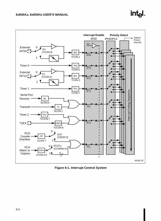
8x930Ax, 8x930Hx USER’S MANUAL
Figure 6-1. Interrupt Control System
IE0
0
1
INT0#
Timer 0
IE1
0
1
INT1#
Timer 1
0
1
0
1
ECF (CMOD.0)
ECCFx (CCAPMx.0)
IT0 (TCON.0)
IT1 (TCON.2)
5
IPH0/IPL0Interrupt Enable Priority Select
EX0
ET0
EX1
ET1
EC
ES
ET2
TF0
CF
CCFx
RI
TI
TF2
EXF2
TF1
PCA Counter
Overflow
PCA Match or Capture
Receive
Transmit
Timer 2
T2EX
Inte
rrup
t Pol
ling
Seq
uenc
e
Highest Priority Interrupt
EA
A5042-02
IEN0
External
External
TCON.7
TCON.3
TCON.5
TCON.1
CCON.4:0
CCON.7
Serial Port
SCON.0
T2CON.7
SCON.1
T2CON.6
6-2

INTERRUPT SYSTEM
-rces in-, onerruptst
rrupts,st flag
6.2 8x930 INTERRUPT SOURCES
Figures 6-1 and 6-2 illustrate the interrupt control system. The 8x930 has eleven interrupt sources; ten maskable sources and the TRAP instruction (always enabled). The maskable souclude two external interrupts (INT0# and INT1#), three timer interrupts (timers 0, 1, and 2)programmable counter array (PCA) interrupt, one serial port interrupt, and three USB inte(one of which doubles as a hub interrupt). Each interrupt (except TRAP) has an interrupt requesflag, which can be set by firmware as well as by hardware (see Table 6-3). For some intehardware clears the request flag when it grants an interrupt. Firmware can clear any requeto cancel an impending interrupt.
Figure 6-2. USB/Hub Interrupt Control System
SOFH.6
ASOFAny Start of Frame SOFIE
HRXD0
HTXD0Transmit
Receive
0
HIFLG
SOFH.5
0
1
IPH1/IPL1IEN1
Interrupt Enable Priority Select
Lowest Priority Interrupt
A5100-02
0
1
0
1
FRXIEx
FTXIEx
FRXDx
FTXDx
USB Endpoint Done
Transmit
Receive1
EF
1
GRSM
URSTUSB Reset
PCON1.3
GSUSUSB
Suspend
USB Resume
ESR
2
1
PCON1.0
PCON1.1
USB Hub
FIFLG, FIFLG1
0
1
0
1
HRXE0
HTXE0
11
ESOF/Hub
FIE, FIE1
HIE
EA
8X930Ax Only
PCON1.4
URDIS
6-3
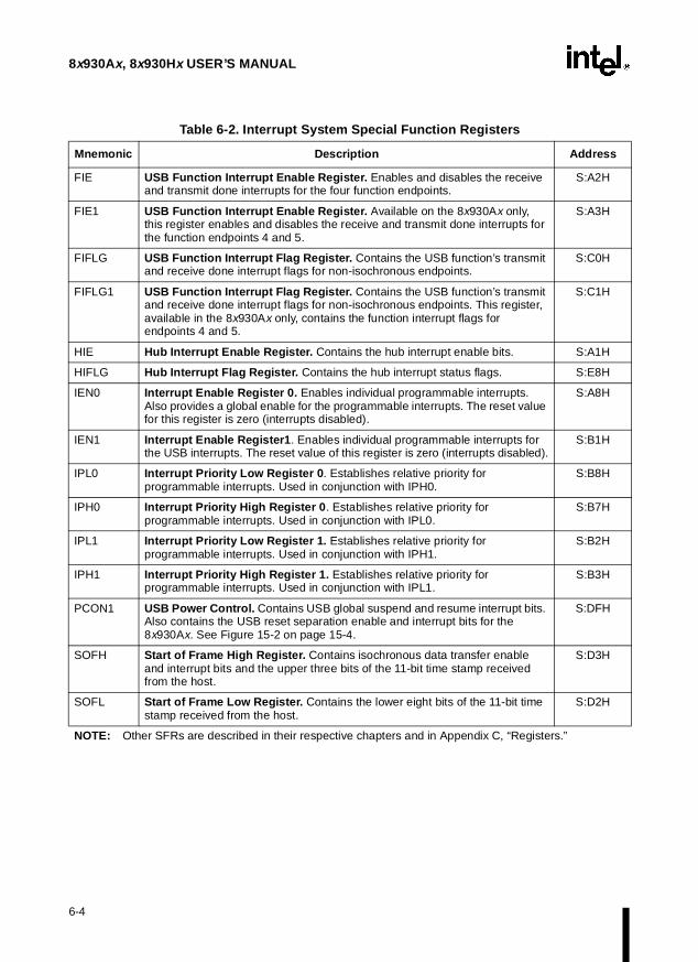
8x930Ax, 8x930Hx USER’S MANUAL
Table 6-2. Interrupt System Special Function Regist ers
Mnemonic Description Address
FIE USB Function Interrupt Enable Register. Enables and disables the receive and transmit done interrupts for the four function endpoints.
S:A2H
FIE1 USB Function Interrupt Enable Register. Available on the 8x930Ax only, this register enables and disables the receive and transmit done interrupts for the function endpoints 4 and 5.
S:A3H
FIFLG USB Function Interrupt Flag Register. Contains the USB function’s transmit and receive done interrupt flags for non-isochronous endpoints.
S:C0H
FIFLG1 USB Function Interrupt Flag Register. Contains the USB function’s transmit and receive done interrupt flags for non-isochronous endpoints. This register, available in the 8x930Ax only, contains the function interrupt flags for endpoints 4 and 5.
S:C1H
HIE Hub Interrupt Enable Register. Contains the hub interrupt enable bits. S:A1H
HIFLG Hub Interrupt Flag Register. Contains the hub interrupt status flags. S:E8H
IEN0 Interrupt Enable Register 0. Enables individual programmable interrupts. Also provides a global enable for the programmable interrupts. The reset value for this register is zero (interrupts disabled).
S:A8H
IEN1 Interrupt Enable Register1 . Enables individual programmable interrupts for the USB interrupts. The reset value of this register is zero (interrupts disabled).
S:B1H
IPL0 Interrupt Priority Low Register 0 . Establishes relative priority for programmable interrupts. Used in conjunction with IPH0.
S:B8H
IPH0 Interrupt Priority High Register 0 . Establishes relative priority for programmable interrupts. Used in conjunction with IPL0.
S:B7H
IPL1 Interrupt Priority Low Register 1. Establishes relative priority for programmable interrupts. Used in conjunction with IPH1.
S:B2H
IPH1 Interrupt Priority High Register 1. Establishes relative priority for programmable interrupts. Used in conjunction with IPL1.
S:B3H
PCON1 USB Power Control. Contains USB global suspend and resume interrupt bits. Also contains the USB reset separation enable and interrupt bits for the 8x930Ax. See Figure 15-2 on page 15-4.
S:DFH
SOFH Start of Frame High Register. Contains isochronous data transfer enable and interrupt bits and the upper three bits of the 11-bit time stamp received from the host.
S:D3H
SOFL Start of Frame Low Register. Contains the lower eight bits of the 11-bit time stamp received from the host.
S:D2H
NOTE: Other SFRs are described in their respective chapters and in Appendix C, “Registers.”
6-4

INTERRUPT SYSTEM
g-e 11-6
tonly ifrvicece
tees state
6.2.1 External Interrupts
External interrupts INT0# and INT1# (INTx#) pins may each be programmed to be level-trigered or edge-triggered, dependent upon bits IT0 and IT1 in the TCON register (see Figuron page 11-8). If ITx = 0, INTx# is triggered by a detected low at the pin. If ITx = 1, INTx# isnegative-edge triggered. External interrupts are enabled with bits EX0 and EX1 (EXx) in theIEN0 register (see Figure 6-12). Events on the external interrupt pins set the interrupt requesflags IEx in TCON. These request bits are cleared by hardware vectors to service routines the interrupt is negative-edge triggered. If the interrupt is level-triggered, the interrupt seroutine must clear the request bit. External hardware must deassert INTx# before the servirou-tine completes, or an additional interrupt is requested. External interrupt pins must be deassertedfor at least four state times prior to a request.
External interrupt pins are sampled once every four state times (a frame length of 666.4 ns at 12MHz). A level-triggered interrupt pin held low or high for any five-state time period guarandetection. Edge-triggered external interrupts must hold the request pin low for at least fivetimes. This ensures edge recognition and sets interrupt request bit EXx. The CPU clears EXx au-tomatically during service routine fetch cycles for edge-triggered interrupts.
Additional interrupts specific to USB and USB hub operation appear in Table 6-4.
Table 6-3. Interrupt Control Matrix
Interrupt Name † GlobalEnable PCA Timer
2Serial Port
Timer 1 INT1# Timer
0 INT0#
Bit Name in IEN0 Register EA EC ET2 ES ET1 EX1 ET0 EX0
Interrupt Priority-Within-Level(10 = Low Priority,1 = High Priority)
NA 7 6 5 4 3 2 1
Bit Names in:IPH0 IPL0
ReservedReserved
IPH0.6IPL0.6
IPH0.5 IPL0.5
IPH0.4 IPL0.4
IPH0.3 IPL0.3
IPH0.2 IPL0.2
IPH0.1 IPL0.1
IPH0.0 IPL0.0
Programmable forNegative-edgeTriggered or Level-triggered Detect?
NA Edge No No No Yes No Yes
Interrupt Request Flag in CCON, T2CON, SCON, or TCON Register
NACCON:
CF,CCFx
T2CON:TF2,EXF2
SCON:RI, TI
TCON:TF1
TCON:IE1
TCON:TF0
TCON:IE0
Interrupt RequestFlag Cleared by Hardware?
No No No No YesEdgeYes,
Level NoYes
EdgeYes,
Level No
ISR Vector Address NA FF:0033H
FF:002BH
FF:0023H
FF:001BH
FF:0013H
FF:000BH
FF:0003H
† The 8x930 also contains a TRAP interrupt, not cleared by hardware, with a vector address of FF007BH. For a discussion of TRAP and other interrupt sources, see “8x930 Interrupt Sources” on page 6-3.
6-5

8x930Ax, 8x930Hx USER’S MANUAL
8) areWhenpt ser-r (see
(seeine. Ind then
6.2.2 Timer Interrupts
Two timer-interrupt request bits TF0 and TF1 (see TCON register, Figure 11-6 on page 11-set by timer overflow (the exception is Timer 0 in Mode 3, see Figure 11-4 on page 11-6). a timer interrupt is generated, the bit is cleared by an on-chip hardware vector to an interruvice routine. Timer interrupts are enabled by bits ET0, ET1, and ET2 in the IEN0 registeFigure 6-12).
Timer 2 interrupts are generated by a logical OR of bits TF2 and EXF2 in register T2CONFigure 11-12 on page 11-17). Neither flag is cleared by a hardware vector to a service routfact, the interrupt service routine must determine if TF2 or EXF2 generated the interrupt, anclear the bit. Timer 2 interrupt is enabled by ET2 in register IEN0.
Table 6-4. USB/Hub Interrupt Control Matrix
Interrupt NameUSB Global
Suspend/Resume and USB Reset †
USB Function [Non-Isochronous
Endpoint]
USB Hub/SOF[Isochronous
Endpoint]
Bit Name in IEN1 Register ESR EF ESOF
Interrupt Priority-Within-Level(10 = Low Priority,1 = High Priority)
10 9 8
Bit Names in:IPH1 IPL1
IPH1.2 IPL1.2
IPH1.1 IPL1.1
IPH1.0 IPL1.0
Programmable forNegative-edgeTriggered or Level-triggered Detect?
N/A N/A N/A
Interrupt Request Flag in PCON1, FIFLG, HIFLG, or SOFH Register
PCON1:GSUSGRSMURST†
FIFLG:FTXDx, FRXDx
x=0,1,2,3
SOFH:ASOF,HIFLG:
HTXD0, HRXD0
Interrupt RequestFlag Cleared by Hardware?
No No No
ISR Vector Address FF:0053H FF:004BH FF:0043H
† USB Reset interrupt applies to the 8x930Ax only.
6-6

INTERRUPT SYSTEM
event
uestsupts.
e CF
r (seee. The
nctionrrupt
global
us da-rupts
inter-
6.3 PROGRAMMABLE COUNTER ARRAY (PCA) INTERRUPT
The programmable counter array (PCA) interrupt is generated by the logical OR of five flags (CCFx) and the PCA timer overflow flag (CF) in the CCON register (see Figure 12-8 onpage 12-14). All PCA interrupts share a common interrupt vector. Bits are not cleared by hard-ware vectors to service routines. Normally, interrupt service routines resolve interrupt reqand clear flag bits. This allows the user to define the relative priorities of the five PCA interr
The PCA interrupt is enabled by bit EC in the IEN0 register (see Figure 6-1). In addition, thflag and each of the CCFx flags must also be individually enabled by bits ECF and ECCFx in reg-isters CMOD and CCAPMx, respectively, for the flag to generate an interrupt (see Figure 12-7on page 12-13 and Figure 12-9 on page 12-16).
NOTECCFx refers to five separate bits, one for each PCA module (CCF0, CCF1, CCF2, CCF3, CCF4). CCAPMx refers to 5 separate registers, one for each PCA module (CCAPM0, CCAPM1, CCAPM2, CCAPM3, CCAPM4).
6.4 SERIAL PORT INTERRUPT
Serial port interrupts are generated by the logical OR of bits RI and TI in the SCON registeFigure 13-2 on page 13-4). Neither flag is cleared by a hardware vector to the service routinservice routine resolves RI or TI interrupt generation and clears the serial port request flag. Theserial port interrupt is enabled by bit ES in the IEN0 register (see Figure 6-12).
6.5 USB INTERRUPTS
There are three types of USB interrupts, as shown in Figure 6-2 on page 6-3: The USB fuinterrupt, used to control the flow of non-isochronous data; the hub/any start-of-frame inte(SOF), used to signal a hub interrupt or to monitor the transfer of isochronous data; and thesuspend/resume interrupt, used to allow USB power control and, for the 8x930Ax only, to providea separate USB interrupt. These interrupts are enabled using the IEN1 register. See Table 6-4 andFigure 6-13.
6.5.1 USB Function Interrupt
The USB function generates two types of interrupts to control the transfer of non-isochronota: the receive done interrupt and the transmit done interrupt. Individual USB function interin the 8x930 are enabled by setting the corresponding bits in the FIE register (Figure 6-3). The8x930Ax, with its six function endpoints, also uses the FIE1 register (Figure 6-4) to enable rupts for endpoints 4 and 5.
NOTEIn order to use any of the USB function interrupts, the EF bit in the IEN1 register must be enabled.
6-7

8x930Ax, 8x930Hx USER’S MANUAL
icate
ll bits ‘0’
The USB Function Interrupt Flag register (FIFLG, as shown in Figure 6-5) is used to indpending function interrupts for a given endpoint. The 8x930Ax, with its six function endpoints,also uses the FIFLG1 register (Figure 6-6) to indicate interrupts for endpoints 4 and 5. For ain FIFLG or FIFLG1, a ‘1’ indicates that an interrupt is actively pending for that endpoint; aindicates that the interrupt is not active. The interrupt status is shown in the FIFLG or FIFLG1register regardless of the state of the corresponding interrupt enable bit in the FIE or FIE1 register(Figures 6-3 and 6-4).
Figure 6-3. FIE: USB Function Interrupt Enable Register
FIE Address: S:A2HReset State: 0000 0000B
Function Interrupt Enable Register. Enables and disables the receive and transmit done interrupts for the four function endpoints.
7 0
FRXIE3 FTXIE3 FRXIE2 FTXIE2 FRXIE1 FTXIE1 FRXIE0 FTXIE0
Bit Number
Bit Mnemonic Function
7 FRXIE3 Function Receive Interrupt Enable 3:
Enables receive done interrupt for endpoint 3 (FRXD3).
6 FTXIE3 Function Transmit Interrupt Enable 3:
Enables transmit done interrupt for endpoint 3 (FTXD3).
5 FRXIE2 Function Receive Interrupt Enable 2:
Enables the receive done interrupt for endpoint 2 (FRXD2).
4 FTXIE2 Function Transmit Interrupt Enable 2:
Enables the transmit done interrupt for endpoint 2 (FTXD2).
3 FRXIE1 Function Receive Interrupt Enable 1:
Enables the receive done interrupt for endpoint 1 (FRXD1).
2 FTXIE1 Function Transmit Interrupt Enable 1:
Enables the transmit done interrupt for endpoint 1 (FTXD1).
1 FRXIE0 Function Receive Interrupt Enable 0:
Enables the receive done interrupt for endpoint 0 (FRXD0).
0 FTXIE0 Function Transmit Interrupt Enable 0:
Enables the transmit done interrupt for endpoint 0 (FTXD0).
NOTE: For all bits, a ‘1’ means the interrupt is enabled and will cause an interrupt to be signaled to the microcontroller. A ‘0’ means the associated interrupt source is disabled and cannot cause an interrupt, even though the interrupt bit’s value is still reflected in the FIFLG register.
6-8

INTERRUPT SYSTEM
ans-
s
Figure 6-4. FIE1: USB Function Interrupt Enable Register
The USB function generates a receive done interrupt for an endpoint x (x = 0–3) by setting theFRXDx bit in the FIFLG or FIFLG1 register (Figures 6-5 and 6-6). Only non-isochronous trfer can cause a receive done interrupt. Receive done interrupts are generated only when all of thefollowing are true:
1. A valid SETUP or OUT token is received to function endpoint x, and
2. Endpoint x is enabled for reception (RXEPEN in EPCON = ‘1’), and
3. Receive is enabled (RXIE = ‘1’) and STALL is disabled (RXSTL = ‘0’) for OUT token(or the token received is a SETUP token), and
4. A data packet is received with no time-out — regardless of transmission errors (CRC, bit-stuffing) or FIFO errors (overrun, underrun), and
5. There is no data sequence PID error.
FIE1 Address: S:A3HReset State: 0000 0000B
Function Interrupt Enable Register 1. Available on the 8x930Ax only, this register enables and disables the receive and transmit done interrupts for function endpoints four and five.
7 0
— — — — FRXIE5 FTXIE5 FRXIE4 FTXIE4
Bit Number
Bit Mnemonic Function
7:4 — Reserved:
3 FRXIE5 Function Receive Done Interrupt Enable 5:
Enables receive done interrupt for endpoint 5 (FTXD5).
2 FTXIE5 Function Transmit Interrupt Enable 5:
Enables the transmit done interrupt for endpoint 5 (FTXD5).
1 FRXIE4 Function Receive Interrupt Enable 4:
Enables the receive done interrupt for endpoint 4 (FRXD4).
0 FTXIE4 Function Transmit Interrupt Enable 4:
Enables the transmit done interrupt for endpoint 4 (FTXD4).
NOTE: When the FRXIE.5:4 or FTXIE.5:4 is set, the interrupt is enabled and it will cause an interrupt to the CPU, when a transmit of receive done flag is set. If the FRXIE.5:4 and FTXIE.5:4 is cleared, the interrupt is disabled. All these bits can be read/write by firmware.
6-9

8x930Ax, 8x930Hx USER’S MANUAL
ission
heck
sfer
in
ission
o
s
Because the FRXDx bit is set and a receive done interrupt is generated regardless of transmerrors, this condition means either:
1. Valid data is waiting to be serviced in the receive FIFO for function endpoint x and that the data was received without error and has been acknowledged; or
2. Data was received with a receive data error and requires firmware intervention to becleared. This could be either a transmission error or a FIFO-related error. You must cfor these conditions and respond accordingly in the interrupt service routine (ISR).
The USB function generates a transmit done interrupt for an endpoint x (x = 0–3†) by setting theFTXDx bit in the FIFLG or FIFLG1 register (Figures 6-5 and 6-6). Only non-isochronous trancan cause a transmit done interrupt. Transmit done interrupts are generated only when all of thefollowing are true:
1. A valid IN token is received to function endpoint x, and
2. Endpoint x is enabled for transmission (TXEPEN = ‘1’), and
3. Transmit is enabled (TXIE = ‘1’) and STALL is disabled (TXSTL = ‘0’), and
4. A data packet/byte count has been loaded in the transmit FIFO and was transmittedresponse to the IN token — regardless of whether or not a FIFO error occurs, and
5. An ACK is received from the host or there was a time-out in the SIE.
Because the FTXDx bit is set and a transmit done interrupt is generated regardless of transmerrors, this condition means either:
1. The transmit data has been transmitted and the host has sent an acknowledgment tindicate that is was successfully received; or
2. A transmit data error occurred during transmission of the data packet, which requireservicing by firmware to be cleared. You must check for these conditions and respond accordingly in the ISR.
NOTESetting an endpoint interrupt’s bit in the Function Interrupt Enable register (FIE or FIE1, as shown in Figures 6-3 and 6-4) means that the interrupt is enabled and will cause an interrupt to be signaled to the microcontroller. Clearing a bit in the FIE register disables the associated interrupt source, which can no longer cause an interrupt even though its value will still be reflected in the FIFLG or FIFLG1 register (Figures 6-5 and 6-6).
† The 8x930Ax can be configured for up to six endpoints, 0-5.
6-10

INTERRUPT SYSTEM
Figure 6-5. FIFLG: USB Function Interrupt Flag Register
FIFLG Address: S:C0HReset State: 0000 0000B
Function Interrupt Flag Register. Contains the USB Function’s Transmit and Receive Done interrupt flags for non-isochronous endpoints.
7 0
FRXD3 FTXD3 FRXD2 FTXD2 FRXD1 FTXD1 FRXD0 FTXD0
Bit Number
Bit Mnemonic Function
7 FRXD3 Function Receive Done Flag, Endpoint 3
6 FTXD3 Function Transmit Done Flag, Endpoint 3
5 FRXD2 Function Receive Done Flag, Endpoint 2
4 FTXD2 Function Transmit Done Flag, Endpoint 2
3 FRXD1 Function Receive Done Flag, Endpoint 1
2 FTXD1 Function Transmit Done Flag, Endpoint 1
1 FRXD0 Function Receive Done Flag, Endpoint 0
0 FTXD0 Function Transmit Done Flag, Endpoint 0
NOTES:1. For all bits in the Interrupt Flag Register, a ‘1’ indicates that an interrupt is actively pending; a ‘0’
indicates that the interrupt is not active. The interrupt status is shown regardless of the state of the corresponding interrupt enable bit in the FIE.
2. Bits are set-only by hardware and clearable in firmware. Firmware can also set the bits for test purposes, allowing the interrupt to be generated in firmware.
3. A set bit indicates either: Valid data waiting to be serviced in the RX FIFO for the indicated endpoint and that the data was received without error and has been acknowledged; or Data was received with a Receive Data Error requiring firmware intervention to be cleared.
6-11

8x930Ax, 8x930Hx USER’S MANUAL
. The timernable
d fromrtificialhen ahe
Figure 6-6. FIFLG1: USB Function Interrupt Flag Register
6.5.2 USB Start-of-frame Interrupt
The USB start-of-frame interrupt (SOF) is used to control the transfer of isochronous data8x930 frame timer attempts to synchronize to the frame time automatically. When the frameis locked to the USB frame time, hardware sets the FTLOCK bit in SOFH (Figure 6-7). To ethe start-of-frame interrupt, set the SOFIE bit in SOFH.
The 8x930 generates a start-of-frame interrupt whenever a start-of-frame packet is receivethe USB lines, or whenever a start-of-frame packet should have been received (i.e., an aSOF). The 8x930 generates an SOF interrupt by setting the ASOF bit in the SOFH SFR. Wstart-of-frame interrupt occurs, the 8x930 loads the current value of the frame timer into tSOFH/SOFL registers (Figures 6-7 and 6-8).
FIFLG1 Address: S:C1HReset State: 0000 0000B
Function Interrupt Flag Register 1. Available on the 8x930Ax only, this register contains the USB Function’s Transmit and Receive Done interrupt flags for non-isochronous endpoints.
7 0
— — — — FRXD5 FTXD5 FRXD4 FTXD4
Bit Number
Bit Mnemonic Function
7:4 — Reserved:
Write zeros to these bits.
3 FTXD5 Function Receive Done Flag, Endpoint 5:
2 FTXD5 Function Transmit Done Flag, Endpoint 5:
1 FRXD4 Function Receive Done Flag, Endpoint 4:
0 FTXD4 Function Transmit Done Flag, Endpoint 4:
NOTES:1. For all bits in the Interrupt Flag Register, a ‘1’ indicates that an interrupt is actively pending; a ‘0’
indicates that the interrupt is not active. The interrupt status is shown regardless of the state of the corresponding interrupt enable bit in the FIE.
2. Bits are set-only by hardware and clearable in firmware. Firmware can also set the bits for test purposes, allowing the interrupt to be generated in firmware.
3. A set bit indicates either: Valid data waiting to be serviced in the RX FIFO for the indicated endpoint and that the data was received without error and has been acknowledged; or Data was received with a Receive Data Error requiring firmware intervention to be cleared.
6-12

INTERRUPT SYSTEM
NOTEThe start-of-frame interrupt shares an interrupt vector with the hub interrupt. When this interrupt is triggered, firmware must examine the ASOF bit in the SOFH SFR to determine that it was the start-of-frame interrupt that was triggered, and not the hub interrupt.
SOFH Address: S:D3HReset State: 0000 0000B
Start of Frame High Register. Contains isochronous data transfer enable and interrupt bits and the upper three bits of the 11-bit time stamp received from the host.
7 0
SOFACK ASOF SOFIE FTLOCK SOFODIS TS10 TS9 TS8
Bit Number
Bit Mnemonic Function
7 SOFACK SOF Token Received without Error (read-only):
When set, this bit indicates that the 11-bit time stamp stored in SOFL and SOFH is valid. This bit is updated every time a SOF token is received from the USB bus, and it is cleared when an artificial SOF is generated by the frame timer. This bit is set and cleared by hardware.
6 ASOF Any Start of Frame:
This bit is set by hardware to indicate that a new frame has started. The interrupt can result either from reception of an actual SOF packet or from an artificially-generated SOF from the frame timer. This interrupt is asserted in hardware even if the frame timer is not locked to the USB bus frame timing. When set, this bit is an indication that either an actual SOF packet was received or an artificial SOF was generated by the frame timer. This bit must be cleared by firmware or inverted and driven to the SOF# pin. The effect of setting this bit by firmware is the same as hardware: the external pin will be driven with an inverted ASOF value for eight TCLKs.
This bit also serves as the SOF interrupt flag. This interrupt is only asserted in hardware if the SOF interrupt is enabled (SOFIE set) and the interrupt channel is enabled.
5 SOFIE SOF Interrupt Enable:
When this bit is set, setting the ASOF bit causes an interrupt request to be generated if the interrupt channel is enabled. Hardware reads but does not write this bit.
4 FTLOCK Frame Timer Locked (read-only):
When set, this bit indicates that the frame timer is presently locked to the USB bus’ frame time. When cleared, this bit indicates that the frame timer is attempting to synchronize to the frame time.
Figure 6-7. SOFH: Start of Frame High Register
6-13

8x930Ax, 8x930Hx USER’S MANUAL
Figure 6-8. SOFL: Start of Frame Low Register
3 SOFODIS SOF# Pin Output Disable:
When set, no low pulse will be driven to the SOF# pin in response to setting the ASOF bit. The SOF# pin will be driven to ‘1’ when SOFODIS is set. When this bit is clear, setting the ASOF bit causes the SOF# pin to be toggled with a low pulse for eight TCLKs.
2:0 TS10:8 Time stamp received from host:
TS10:8 are the upper three bits of the 11-bit frame number issued with an SOF token. This time stamp is valid only if the SOFACK bit is set.
SOFL Address: S:D2HReset State: 0000 0000B
Start-of-Frame Low Register. Contains the lower eight bits of the 11-bit time stamp received from the host.
7 0
TS7:0
Bit Number
Bit Mnemonic Function
7:0 TS7:0 Time stamp received from host:
This time stamp is valid only if the SOFACK bit in the SOFH register is set. TS7:0 are the lower eight bits of the 11-bit frame number issued with a SOF token. If an artificial SOF is generated, the time stamp remains at its previous value and it is up to firmware to update it. These bits are set and cleared by hardware.
SOFH (Continued) Address: S:D3HReset State: 0000 0000B
Start of Frame High Register. Contains isochronous data transfer enable and interrupt bits and the upper three bits of the 11-bit time stamp received from the host.
7 0
SOFACK ASOF SOFIE FTLOCK SOFODIS TS10 TS9 TS8
Bit Number
Bit Mnemonic Function
Figure 6-7. SOFH: Start of Frame High Register (Continued)
6-14

INTERRUPT SYSTEM
mory r
d
ould beis hin thech timer
sfer,
r
0.
The 8x930 uses the start-of-frame interrupt to signal either of two complementary events:
1. When transmitting: The next isochronous data packet needs to be retrieved from meand loaded into the transmit FIFO in preparation for transmission in the next frame; o
2. When receiving: An isochronous packet has been received in the previous frame anneeds to be retrieved from the receive FIFO.
Since the start-of-frame packet could be corrupted, there is a chance that a new frame cstarted without successful reception of the SOF packet. For this reason, an artificial SOF pro-vided. The frame timer signals a time-out when an SOF packet has not been received witallotted amount of time. In this fashion, the 8x930 generates an SOF interrupt reliably once eaframe within 1 µs of accuracy, except when this interrupt is suspended or when the framegets out-of-sync with the USB bus frame time.
In summary, in order to utilize the USB start-of-frame functionality for isochronous data tranthe following must all be true:
1. The global enable bit must be set. That is, the EA bit must be set in the IEN0 registe(Figure 6-12).
2. The isochronous endpoint any SOF interrupt must be enabled. That is, the ESOF bit must be set in the IEN1 register (Figure 6-13).
3. The start-of-frame interrupt must be enabled. That is, the SOFIE bit must be set in the SOFH Register (Figure 6-7).
NOTEThe SOF interrupt is brought out to an external pin (SOF#) in order to provide a 1 ms pulse, subject to the accuracy of the USB start-of-frame. This pin is enabled by clearing the SOFODIS bit in the SOFH register.
6.5.3 USB Hub Interrupt
The USB hub interrupt is used to signal a receive done or transmit done for hub endpoint
To enable the hub interrupt:
1. Set the global enable bit (EA) in the IEN0 register (Figure 6-12)
2. Enable the hub endpoint 0 transmit done and receive done interrupts individually:
a. To enable the receive done interrupt, set the HRXE0 bit in the Hub Interrupt Enable SFR (HIE, as shown in Figure 6-9)
b. To enable the transmit done interrupt, set the HTXE0 bit in HIE
6-15

8x930Ax, 8x930Hx USER’S MANUAL
g; a
Figure 6-9. HIE: Hub Interrupt Enable Register
The USB Hub Interrupt Flag Register (HIFLG, as shown in Figure 6-10) is used to indicate pend-ing hub interrupts. For all bits in HIFLG, a ‘1’ indicates that an interrupt is actively pendin‘0’ indicates that the interrupt is not active. The interrupt status is shown in the HIFLG registerregardless of the state of the corresponding interrupt enable bit in the HIE Register (Figure 6-9).
NOTEThe hub interrupt shares an interrupt vector with the start-of-frame interrupt. When this interrupt is triggered, firmware must examine the HIFLG SFR to determine that it was the hub interrupt that was triggered and not the start-of-frame interrupt.
HIE Address: S:A1HReset State: 0xxx xx00B
Hub Interrupt Enable Register. Enables and disables the receive and transmit done interrupts for hub endpoint 0.
7 0
— — — — — HRXE0 HTXE0
Bit Number
Bit Mnemonic Function
7:2 — Reserved:
Write zeros to these bits.
1 HRXE0 HRXE0:
Enable the hub endpoint 0 receive done interrupt (HRXD0).†
0 HTXE0 HTXE0:
Enable the hub endpoint 0 transmit done interrupt (HTXD0).†
† For both bits, a ‘1’ means the interrupt is enabled, and will cause an interrupt to be signaled to the microcontroller. A ‘0’ means the associated interrupt source is disabled and cannot cause an interrupt, even though its value is still reflected in the HIFLG register.
6-16

INTERRUPT SYSTEM
Figure 6-10. HIFLG: Hub Interrupt Status Register
HIFLG Address: S:E8HReset State: 0xxx xx00B
Hub Interrupt Flag Register. Contains the hub’s transmit and receive done interrupt flags for hub endpoint 0.
7 0
— — — — — HRXD0 HTXD0
Bit Number
Bit Mnemonic Function
7:2 — Reserved:
Write zeros to these bits.
1 HRXD0 Hub Receive Done, Endpoint 0.:
Hardware sets this bit to indicate that there is either: (1) valid data waiting to be serviced in the receive data buffer for hub endpoint 0 and that the data was received without error and has been acknowledged; or (2) that data was received with a FIFO error requiring firmware intervention to be cleared.
0 HTXD0 Hub Transmit Done, Endpoint 0:
Hardware sets this bit to indicate that one of two conditions exists in the transmit data buffer for hub endpoint 0: (1) the transmit data has been transmitted and the host has sent acknowledgment which was successfully received; or (2) a FIFO-related error occurred during transmission of the data packet, which requires servicing by firmware to be cleared.
NOTES:1. Note that because the HIFLG appears in the first SFR column, it is a bit-addressable SFR. All bits
are set in hardware and cleared by firmware. Firmware can also set these bits for test purposes, allowing the interrupt to be generated by firmware.
2. For both HRXD0 and HTXD0, a ‘1’ indicates that an interrupt is actively pending; a ‘0’ indicates that the interrupt is not active. The interrupt status is shown regardless of the state of the corresponding interrupt enable bit in the HIE.
6-17

8x930Ax, 8x930Hx USER’S MANUAL
r
activitye” on
etected one, thept. For
f the-up has tond/re-
U in
modeake-
. when iterateshub.
6.5.4 USB Global Suspend/Resume Interrupt
The 8x930 supports USB power control through firmware. The USB power control registe(PCON1, as shown in Figure 15-2 on page 15-4) facilitates USB power control of the 8x930, in-cluding global suspend/resume and USB function resume.
NOTEOn the 8x930Ax only, the global suspend/resume interrupt shares an interrupt vector with the USB reset interrupt. When this interrupt is triggered, firmware must examine the GSUS and GRSM bits in the PCON1 SFR (Figure 15-2 on page 15-4) to determine that it was the global suspend/resume interrupt that was triggered, and not the USB reset interrupt.
6.5.4.1 Global Sus pend
When a global suspend is detected by the 8x930, the global suspend bit (GSUS of PCON1) is setand the global suspend/resume interrupt is generated. Global suspend is defined as bus infor more than 3 ms on the USB lines. For additional information, see “Global Suspend Modpage 15-8.
6.5.4.2 Global Resume
When a global resume is detected by the 8x930, the global resume bit (GRSM of PCON1) is sand the global suspend/resume interrupt is generated. As soon as resume signaling is detthe USB lines, the oscillator is restarted. After executing the resume interrupt service routin8x930 resumes operation from where it was when it was interrupted by the suspend interruadditional information, see “Global Resume Mode” on page 15-10.
6.5.4.3 USB Remote Wake-up
The 8x930 can also initiate resume signaling to the USB lines through remote wake-up oUSB function while it is in powerdown/idle mode. While in powerdown mode, remote wakehas to be initiated through assertion of an enabled external interrupt. The external interruptbe enabled and it must be configured with level trigger and with higher priority than a suspesume interrupt. An external interrupt restarts the clocks to the 8x930 and program executionbranches to the external interrupt service routine.
Within this external interrupt service routine, you must set the remote wakeup bit (RWPCON1) to drive resume signaling on the USB lines to the host or upstream hub. After executingthe external ISR, the program continues execution from where it was put into powerdown and the 8x930 resumes normal operation. For additional information, see “USB Remote Wup” on page 15-10.
6.5.5 8x930Ax USB Reset Separation
The 8x930Ax features an optional USB reset that functions independently from the chip resetWhen the PCON1 SFR’s URDIS bit is set, the MCS 251 core and peripherals will not reseta USB reset signal is detected. After an 8x930Ax with URDIS set detects a USB reset signal,resets all the USB blocks (including the USB SFRs), sets the URST bit in PCON1, and gena USB reset interrupt. USB reset signals can originate only from the host PC or upstream
6-18

INTERRUPT SYSTEM
gen- reset 15-3)ing
lock
e out-
rm the
NOTEThe use of a separate USB reset is recommended only for applications where the device is required to be operated continually, even when the PC is powered-off. All other applications are advised against using the separate USB reset. Leaving the URDIS bit clear will ensure a robust, chip-level reset.
The USB reset must be implemented partially in firmware, including an initialization routine as part of chip start-up. To ensure compliance with USB-specified timing constraints and minimize the potential for data corruption, you must implement flag checking as part of your main routine, subroutines, and ISRs. These requirements increase the complexity of your firmware code.
If the 8x930Ax is in powerdown or suspend mode when the separate USB reset interrupt iserated, the device will wake up from powerdown or suspend mode upon receiving the USBsignal. The ISR of a bus-powered device must set the LC bit of PCON (Figure 15-1 on pagein order to operate at 3 MHz. This ensures that the device meets the 100 mA current limit durenumeration, as required by the Universal Serial Bus Specification. Self-powered devices (i.e.,devices drawing less than 100mA from the USB wires) may choose not to switch to Low Cmode after detecting the USB reset.
NOTEIf desired, your firmware can handle the separate USB reset without using an ISR. To do this, you must clear the ESR bit in the IEN1 SFR. The USB reset hardware operations will still take place, but the ISR will not be called. That is, step 1 and step 2 under “USB Reset Hardware Operations” on page 6-22 will still occur, but step 3 will not. Your firmware must poll the URST flag periodically to detect the USB reset and take the appropriate action.
Since the global suspend and global resume interrupts share the same interrupt vector as USB reset, your firmware must also poll the GRSM and GSUS bits in PCON1 to detect global suspend or resume.
If, instead, you choose to implement a separate USB reset using an ISR, follow the procedurlined in the following subsections and shown in Figure 6-11.
6.5.5.1 Initialization Required for USB Reset
Because USB reset implementation depends heavily on firmware, your code must perfofollowing initialization prior to execution of the main routine (See Figure 6-11):
1. To enable the USB reset interrupt on the 8x930Ax, your initialization routine must set thefollowing bits to ‘1’:
a. the EA bit of IEN0 (Figure 6-12)
b. the ESR bit of IEN1 (Figure 6-13)
c. the URDIS bit of PCON1 (Figure 15-2 on page 15-4)
6-19

8x930Ax, 8x930Hx USER’S MANUAL
n
ts in
2. Use bit 2 of IPH1/IPL1 to set the priority of the USB reset interrupt (See “Interrupt Priorities” on page 6-27).
NOTEIt is recommended that you set the USB reset interrupt to the highest priority.
3. After enabling the USB reset interrupt and assigning it a priority, your initialization routine should clear the USB_RST_FLG flag. This flag is a global variable declared iyour firmware, not a bit in an SFR.
This flag, an indicator that a USB reset has occurred, will be examined at various poinyour main routine, subroutines, and ISRs.
6-20

INTERRUPT SYSTEM
Figure 6-11. USB Reset Separation Operating Model
No
Initialization Routine: Set IEN0.EA; Set EN1.ESR;
Set PCON1.URDIS; Set Interrupt Priority; USB_RST_FLG = 0;
USB_RST_FLG = 1?
Periodically Test USB_RST_FLG
Yes
Main Routine: (normal processing
until interrupt occurs)
Continue with Main Routine
Continue with Main Routine
Clear USB_RST_FLG; Initialize USB-related SFRs;
Flush USB FIFOs;
USB Initialization Routine
Check PCON1.URST
USB Reset, Global Suspend, Resume ISR
Clear PCON1.URST; USB_RST_FLG = 1
(Bus Powered?– Set PCON.LC)
Perform Global Suspend/Resume
ISR
ISR Complete
= 0= 1
US
B r
eset
trig
gere
d
Loop
con
tinuo
usly
USB Reset Hardware
Reset all USB blocks; Set PCON.URST;
Generate USB Reset Interrupt;
A5206-01
6-21

8x930Ax, 8x930Hx USER’S MANUAL
y the
,
. This
IS
a
resume
must page
e.
this that
er to
n be
6.5.5.2 USB Reset Hardware Operations
When the host initiates a USB reset signal, the following series of events is performed b8x930Ax hardware (See Figure 6-11):
1. Upon detecting a USB reset signal, the 8x930Ax hardware resets all the USB blocks (i.e.the FIFOs, the SIU, the SIE, and the USB transceiver).
As a result of this process, all USB-related SFRs are reset to their default reset statesincludes EPINDEX, EPCON, SOFL, SOFH, FIE, FIFLG, FADDR, TXSTAT, TXDAT, TXCON, TXFLG, TXCNTL, TXCNTH, RXSTAT, RXDAT, RXCON, RXFLG, RXCNTL, RXCNTH, and PCON1. Note that PCON1 is only partially reset — the URDand URST bits retain their original values.
Because of this hardware reset, any USB-related operations (e.g., MOV TXDAT,A) will not provide valid data.
2. The 8x930Ax sets the PCON1.URST bit to indicate a USB reset to the ISR.
3. If the ESR bit in IEN1 is set, the 8x930Ax generates a USB reset interrupt, which causesbranch to the interrupt service routine whose vector is located at FF:0053H. This ISRservices both the USB reset interrupt and the global suspend/resume interrupt.
6.5.5.3 USB Reset ISR
Because the USB reset interrupt shares an interrupt vector with the USB global suspend/interrupt, the interrupt service routine must play a dual role. The ISR must first check PCON1’sURST bit to ensure that this interrupt is indeed a USB reset interrupt.
If URST = ‘0’, then this interrupt must be a global suspend/resume interrupt and the ISRbranch to service that type of interrupt. See “USB Global Suspend/Resume Interrupt” on6-18 for a description of this portion of the ISR.
If the URST bit is set to ‘1’, then this interrupt is a USB reset interrupt. The ISR must performthe following procedure (See Figure 6-11):
1. Clear PCON1’s URST bit — to indicate that the USB reset interrupt has been serviced.
2. Set the user flag USB_RST_FLG that was cleared as part of your initialization routin
This flag is discussed in “Initialization Required for USB Reset” on page 6-19. Settingflag is necessary to inform your firmware routines that a USB reset has occurred andUSB initialization must be performed.
3. Bus-powered devices must set the LC bit of PCON (Figure 15-1 on page 15-3) in ordoperate at 3 MHz. This ensures that the device meets the Universal Serial Bus Specification’s 100 mA current limit during enumeration.
4. Restore any register values and return from interrupt.
The rest of the USB reset procedure will be initiated by a USB initialization routine that cacalled from the main routine, subroutines, or other ISRs.
6-22

INTERRUPT SYSTEM
ializedrrupt is to
which
n
trans-
e our
codepoint,pletee
6.5.5.4 Main Routine Considerations
Although the USB-related SFRs were reset by the USB reset ISR, they must also be initby a special USB initialization routine called by the main routine. Since the USB reset intecan occur at any time, the only way the main routine will know that a USB reset occurredperiodically check the USB reset flag (USB_RST_FLG). This is the firmware flag that was set inStep 2 of the “USB Reset ISR” on page 6-22.
When a set reset flag is detected, the main routine branches to a USB initialization routine,performs the following tasks (See Figure 6-11):
1. Clear the user flag USB_RST_FLG.
Clearing this flag indicates that USB initialization is not required. Clear this flag first icase a second USB reset occurs during this initialization routine, rendering this initialization invalid.
2. Initialize the USB-related SFRs to the values required by your program.
If your application requires any other SFRs to be initialized upon USB reset (e.g., SCON), now is the time to do so.
3. Restore any USB-related user flags specific to your application.
4. Flush all USB FIFOs. This is done by setting RXCLR in RXCON and TXCLR in TXCON. This must be done for each function endpoint.
5. Return to the calling routine.
At this point, the main routine can resume normal processing. Eventually, the host PC will mit a SETUP token. This will trigger an interrupt that will perform USB enumeration.
NOTEUSB specifications require that all devices must be able to accept a device address via a SET_ADDRESS command no later than 10 ms after the reset is removed.
It is recommended that you ensure that the total time required for the following is less than 10ms:
1. The time to complete and exit from the USB reset ISR (accounting for latency — see“Interrupt Processing” on page 6-32)
2. The time for the maximum number of instructions that could execute before your codrecognizes that a USB reset has occurred (by checking USB_RST_FLG) and calls yUSB initialization routine
3. The time to execute your USB initialization routine
This time constraint may require you to check USB_RST_FLG at multiple points in your (and within any ISRs that may take longer than 10ms to perform). By inserting this checkyour program can branch from a routine (or ISR) after the USB reset without having to comthe routine (or ISR). Your program can continue the interrupted routine after ensuring that thdevice is ready for USB enumeration.
6-23

8x930Ax, 8x930Hx USER’S MANUAL
, theween
d by
r, all
CAUTIONIf a USB reset interrupt occurs during execution of a USB receive ISR (e.g., receive done or start-of-frame), the 8x930Ax will reset the USB hardware. This will render invalid any data received during the USB transfer. If this is not detected by your firmware, misprocessing can occur.
The risk of USB reset-related misprocessing can be reduced if your USB receive/transmit ISRscheck USB_RST_FLG before returning. If this flag is set, your code should branch to the USBinitialization routine to initialize the USB-related SFRs and flush the FIFOs. If this is doneonly potential opportunity for misprocessing would be if the USB reset interrupt occurs betthe test of USB_RST_FLG and the branch to the USB initialization routine.
NOTEBecause of the risk of misprocessing, however slight, it is recommended that applications that will not substantially benefit from a separate USB reset disable this option (by leaving the URDIS bit in PCON1 cleared) to simplify firmware coding and ensure a robust, chip-level reset.
6.6 INTERRUPT ENABLE
Each interrupt source (with the exception of TRAP) may be individually enabled or disablethe appropriate interrupt enable bit in the IEN0 register at S:A8H (see Figure 6-12) or the IEN1register at S:B1H (see Figure 6-13). Note IEN0 also contains a global disable bit (EA). If EA isset, interrupts are individually enabled or disabled by bits in IEN0 and IEN1. If EA is cleainterrupts are disabled.
6-24

INTERRUPT SYSTEM
Figure 6-12. IEN0: Interrupt Enable Register 0
IEN0 Address: S:A8HReset State: 0000 0000B
Interrupt Enable Register 0. IEN0 contains two types of interrupt enable bits. The global enable bit (EA) enables/disables all of the interrupts (including those in IEN1), except the TRAP interrupt, which is always enabled. The remaining bits enable/disable the other individual interrupts.
7 0
EA EC ET2 ES ET1 EX1 ET0 EX0
Bit Number
Bit Mnemonic Function
7 EA Global Interrupt Enable:
Setting this bit enables all interrupts that are individually enabled by bits 0–6 of this register, as well as the interrupts enabled by the bits in the IEN1 SFR.
Clearing this bit disables all interrupts, except the TRAP interrupt, which is always enabled.
6 EC PCA Interrupt Enable:
Setting this bit enables the PCA interrupt.
5 ET2 Timer 2 Overflow Interrupt Enable:
Setting this bit enables the timer 2 overflow interrupt.
4 ES Serial I/O Port Interrupt Enable:
Setting this bit enables the serial I/O port interrupt.
3 ET1 Timer 1 Overflow Interrupt Enable:
Setting this bit enables the timer 1 overflow interrupt.
2 EX1 External Interrupt 1 Enable:
Setting this bit enables external interrupt 1.
1 ET0 Timer 0 Overflow Interrupt Enable:
Setting this bit enables the timer 0 overflow interrupt.
0 EX0 External Interrupt 0 Enable:
Setting this bit enables external interrupt 0.
6-25

8x930Ax, 8x930Hx USER’S MANUAL
Figure 6-13. IEN1: USB Interrupt Enable Register
IEN1 Address: S:B1HReset State: xxxx x000H
Interrupt Enable Register 1. Contains the enable bits for the USB interrupts.
7 0
— — — — — ESR EF ESOF
Bit Number
Bit Mnemonic Function
7:3 — Reserved:
Values read from these bits are indeterminate. Write zeros to these bits.
2 ESR Enable Suspend/Resume:
USB global suspend/resume interrupt enable bit.
1 EF Enable Function:
Transmit/Receive Done interrupt enable bit for non-isochronous USB function endpoints.
0 ESOF Enable USB Hub/Start of Frame:
Any start-of-frame interrupt enable for isochronous endpoints, or USB hub interrupt enable.
6-26

INTERRUPT SYSTEM
d to
in-there re-
6-6).
6.7 INTERRUPT PRIORITIES
Ten of the eleven 8x930 interrupt sources (TRAP excluded) may be individually programmeone of four priority levels. This is accomplished with the IPHX.x/IPLX.x bit pairs in the interruptpriority high (IPH1/IPH0 in Figure 6-14 and 6-16) and interrupt priority low (IPL1/IPL0) regis-ters (Figures 6-15 and 6-17). Specify the priority level as shown in Table 6-5 using IPH0.x (orIPH1.x) as the MSB and IPL0.x (or IPL1.x) as the LSB.
A low-priority interrupt is always interrupted by a higher priority interrupt but not by anotherterrupt of equal or lower priority. The highest priority interrupt is not interrupted by any ointerrupt source. Higher priority interrupts are serviced before lower priority interrupts. Thsponse to simultaneous occurrence of equal priority interrupts (i.e., sampled within the same four-state interrupt cycle) is determined by a hardware priority-within-level resolver (see Table
Table 6-5. Level of Priority
Priority Level IPH1. x, IPL1.x IPH0.x, IPL0.x
0 Lowest Priority 00 00
1 01 01
2 10 10
3 Highest Priority 11 11
Table 6-6. Interrupt Priority Within Level
Priority Number Interrupt Name
1 (Highest Priority) INT0#
2 Timer 0
3 INT1#
4 Timer 1
5 Serial Port
6 Timer 2
7 PCA
8 USB Hub / SOF
9 USB Function
10 USB Global Suspend/Resume
6-27

8x930Ax, 8x930Hx USER’S MANUAL
Figure 6-14. IPH0: Interrupt Priority High Register 0
IPH0 Address: S:B7HReset State: x000 0000B
Interrupt Priority High Control Register 0. IPH0, together with IPL0, assigns each interrupt in IEN0 a priority level from 0 (lowest) to 3 (highest):
IPH0.x IPL0.x Priority Level
0 0 0 (lowest priority)
0 1 1
1 0 2
1 1 3 (highest priority)
7 0
— IPH0.6 IPH0.5 IPH0.4 IPH0.3 IPH0.2 IPH0.1 IPH0.0
Bit Number
Bit Mnemonic Function
7 — Reserved. The value read from this bit is indeterminate. Write a zero to this bit.
6 IPH0.6 PCA Interrupt Priority Bit High
5 IPH0.5 Timer 2 Overflow Interrupt Priority Bit High
4 IPH0.4 Serial I/O Port Interrupt Priority Bit High
3 IPH0.3 Timer 1 Overflow Interrupt Priority Bit High
2 IPH0.2 External Interrupt 1 Priority Bit High
1 IPH0.1 Timer 0 Overflow Interrupt Priority Bit High
0 IPH0.0 External Interrupt 0 Priority Bit High
6-28

INTERRUPT SYSTEM
Figure 6-15. IPL0: Interrupt Priority Low Register 0
IPL0 Address: S:B8HReset State: x000 0000B
Interrupt Priority Low Control Register 0. IPL0, together with IPH0, assigns each interrupt in IEN0 a priority level from 0 (lowest) to 3 (highest):
IPH0.x IPL0.x Priority Level
0 0 0 (lowest priority)
0 1 1
1 0 2
1 1 3 (highest priority)
7 0
— IPL0.6 IPL0.5 IPL0.4 IPL0.3 IPL0.2 IPL0.1 IPL0.0
Bit Number
Bit Mnemonic Function
7 — Reserved. The value read from this bit is indeterminate. Write a zero to this bit.
6 IPL0.6 PCA Interrupt Priority Bit Low
5 IPL0.5 Timer 2 Overflow Interrupt Priority Bit Low
4 IPL0.4 Serial I/O Port Interrupt Priority Bit Low
3 IPL0.3 Timer 1 Overflow Interrupt Priority Bit Low
2 IPL0.2 External Interrupt 1 Priority Bit Low
1 IPL0.1 Timer 0 Overflow Interrupt Priority Bit Low
0 IPL0.0 External Interrupt 0 Priority Bit Low
6-29

8x930Ax, 8x930Hx USER’S MANUAL
Figure 6-16. IPH1: Interrupt Priority High Register 1
IPH1 Address: S:B3HReset State: x000 0000B
Interrupt Priority High Control Register 1. IPH1, together with IPL1, assigns each interrupt in IEN1 a priority level from 0 (lowest) to 3 (highest):
IPH1.x IPL1.x Priority Level
0 0 0 (lowest priority)
0 1 1
1 0 2
1 1 3 (highest priority)
7 0
— — — — — IPH1.2 IPH1.1 IPH1.0
Bit Number
Bit Mnemonic Function
7:3 — Reserved:
Values read from these bits are indeterminate. Write zeros to these bits.
2 IPH1.2 Global Suspend/Resume Interrupt Priority Bit High
1 IPH1.1 USB Function Interrupt Priority Bit High
0 IPH1.0 USB Hub/SOF Interrupt Priority Bit High
6-30

INTERRUPT SYSTEM
Figure 6-17. IPL1: Interrupt Priority Low Register 1
IPL1 Address: S:B2HReset State: x000 0000B
Interrupt Priority Low Control Register 1. IPL1, together with IPH1, assigns each interrupt in IEN1 a priority level from 0 (lowest) to 3 (highest):
IPH1.x IPL1.x Priority Level
0 0 0 (lowest priority)
0 1 1
1 0 2
1 1 3 (highest priority)
7 0
— — — — — IPL1.2 IPL1.1 IPL1.0
Bit Number
Bit Mnemonic Function
7:3 — Reserved:
Values read from these bits are indeterminate. Write zeros to these bits.
2 IPL1.2 Global Suspend/Resume Interrupt Priority Bit Low
1 IPL1.1 USB Function Interrupt Priority Bit Low
0 IPL1.0 USB Hub/SOF Interrupt Priority Bit Low
6-31

8x930Ax, 8x930Hx USER’S MANUAL
upt and
in thethec dueditions
quenceare notources, page-
6.8 INTERRUPT PROCESSING
Interrupt processing is a dynamic operation that begins when a source requests an interrlasts until the execution of the first instruction in the interrupt service routine (see Figure 6-18).Response time is the amount of time between the interrupt request and the resulting break current instruction stream. Latency is the amount of time between the interrupt request and execution of the first instruction in the interrupt service routine. These periods are dynamito the presence of both fixed-time sequences and several variable conditions. These concontribute to total elapsed time.
Figure 6-18. The Interrupt Process
Both response time and latency begin with the request. The subsequent minimum fixed secomprises the interrupt sample, poll, and request operations. The variables consist of (but limited to): specific instructions in use at request time, internal versus external interrupt srequests, internal versus external program operation, stack location, presence of wait statemode operation, and branch pointer length.
NOTEIn the following discussion, external interrupt request pins are assumed to be inactive for at least four state times prior to assertion. In this chapter all external hardware signals maintain some setup period (i.e., less than one state time). Signals must meet VIH and VIL specifications prior to any state time under discussion. This setup state time is not included in examples or calculations for either response or latency.
OSC
Ending Instructions Push PC
A4153-01
State Time
External Interrupt Request
ISR
Latency
Response Time
Call ISR
6-32

INTERRUPT SYSTEM
inter-e ad-ations
4 poll
r
time,
efini-vari-rrupthitec-).
before
nterrupt8). Re--e
6.8.1 Minimum Fixed Interrupt Time
All interrupts are sampled or polled every four state-times (see Figure 6-18). Two of eight rupts are latched and polled per state time within any given window of four state-times. Onditional state time is required for a context switch request. For code branches to jump locin the current 64-Kbyte memory region (compatible with MCS 51 microcontrollers), the contextswitch time is 11 states. Therefore, the minimum fixed poll and request time is 16 states (states + 1 request state + 11 states for the context switch = 16 state times).
Therefore, this minimum fixed period rests upon four assumptions:
• The source request is an internal interrupt with high enough priority to take precedence oveother potential interrupts,
• The request is coincident with internal execution and needs no instruction completion
• The program uses an internal stack location, and
• The ISR is in on-chip ROM.
6.8.2 Variable Interrupt Parameters
Both response time and latency calculations contain fixed and variable components. By dtion, it is often difficult to predict exact timing calculations for real-time requests. One large able is the completion time of an instruction cycle coincident with the occurrence of an interequest. Worst-case predictions typically use the longest-executing instruction in an arcture’s code set. In the case of the 8x930, the longest-executing instruction is a 16-bit divide (DIVHowever, even this 21- state instruction may have only 1 or 2 remaining states to completethe interrupt system injects a context switch. This uncertainty affects both response time and la-tency.
6.8.2.1 Response Time Variables
Response time is defined as the start of a dynamic time period when a source requests an iand lasts until a break in the current instruction execution stream occurs (see Figure 6-1sponse time (and therefore latency) is affected by two primary factors: the incidence of the request relative to the four-state-time sample window and the completion time of instructions in thresponse period (i.e., shorter instructions complete earlier than longer instructions).
NOTEExternal interrupt signals require one additional state time in comparison to internal interrupts. This is necessary to sample and latch the pin value prior to a poll of interrupts. The sample occurs in the first half of the state time and the poll/request occurs in the second half of the next state time. Therefore, this sample and poll/request portion of the minimum fixed response and latency time is five states for internal interrupts and six states for external interrupts. External interrupts must remain active for at least five state times to guarantee interrupt recognition when the request occurs immediately after a sample has been taken (i.e., requested in the second half of a sample state time).
6-33
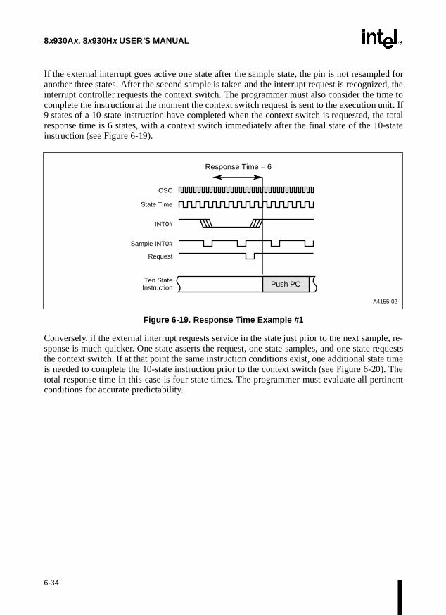
8x930Ax, 8x930Hx USER’S MANUAL
led forzed, theime tounit. Ifhe total-state
le, re-uests time). Thertinent
If the external interrupt goes active one state after the sample state, the pin is not resampanother three states. After the second sample is taken and the interrupt request is recogniinterrupt controller requests the context switch. The programmer must also consider the tcomplete the instruction at the moment the context switch request is sent to the execution 9 states of a 10-state instruction have completed when the context switch is requested, tresponse time is 6 states, with a context switch immediately after the final state of the 10instruction (see Figure 6-19).
Figure 6-19. Response Time Example #1
Conversely, if the external interrupt requests service in the state just prior to the next sampsponse is much quicker. One state asserts the request, one state samples, and one state reqthe context switch. If at that point the same instruction conditions exist, one additional stateis needed to complete the 10-state instruction prior to the context switch (see Figure 6-20total response time in this case is four state times. The programmer must evaluate all peconditions for accurate predictability.
OSC
State Time
INT0#
Sample INT0#
Response Time = 6
Ten State Instruction
Request
Push PC
A4155-02
6-34

INTERRUPT SYSTEM
one DIV isriabletency
Figure 6-20. Response Time Example #2
6.8.2.2 Computation of Worst-case Latency With Variables
Worst-case latency calculations assume that the longest 8x930 instruction used in the programmust fully execute prior to a context switch. The instruction execution time is reduced bystate with the assumption the instruction state overlaps the request state (therefore, 16-bit21 state times - 1 = 20 states for latency calculations). The calculations add fixed and vainterrupt times (see Table 6-7) to this instruction time to predict latency. The worst-case la(both fixed and variable times included) is expressed by a pseudo-formula:
Table 6-7. Interrupt Latency Variables
VariableINT0#,INT1#,T2EX
ExternalExecution
PageMode
>64KJump toISR (1)
ExternalMemory
Wait State
External Stack
<64K (1)
ExternalStack
>64K (1)
ExternalStack
Wait State
Number of
States Added
1 2 1 8 1 perbus cycle 4 8 1 per
bus cycle
NOTES:1. <64K/>64K means inside/outside the 64-Kbyte memory region where code is executing.2. Base-case fixed time is 16 states and assumes:
— A 2-byte instruction is the first ISR byte. — Internal execution
— <64K jump to ISR — Internal stack
— Internal peripheral interrupt
OSC
State Time
INT0#
Sample INT0#
Response Time = 4
Ten State Instruction
Request
Push PC
A4154-02
FIXED_TIME VARIABLES LONGEST_INSTRUCTION+ + MAXIMUM LATENCY PREDICTION=
6-35

8x930Ax, 8x930Hx USER’S MANUAL
nd theps forent 21-est one
occur. state
es arelatency(less
t at aendixware-
int
r
he in-es at
om-
6.8.2.3 Latency Calculations
Assume the use of a zero-wait-state external memory where current instructions, the ISR, astack are located within the same 64-Kbyte memory region (compatible with memory maMCS 51 microcontrollers.) Further, assume there are 3 states yet to complete in the currstate DIV instruction when INT0# requests service. Also assume INT0# has made the requstate prior to the sample state (as in Figure 6-20). Unlike Figure 6-20, the response time for thisassumption is three state times as the current instruction completes in time for the branch toLatency calculations begin with the minimum fixed latency of 16 states. From Table 6-7, oneis added for an INT0# request from external hardware; two states are added for external execu-tion; and four states for an external stack in the current 64-Kbyte region. Finally, three statadded for the current instruction to complete. The actual latency is 26 states. Worst-case calculations predict 43 states for this example due to inclusion of total DIV instruction time one state).
6.8.2.4 Blocking Conditions
If all enable and priority requirements have been met, a single prioritized interrupt requestime generates a vector cycle to an interrupt service routine (see CALL instructions in AppA, “Instruction Set Reference”). There are three causes of blocking conditions with hardgenerated vectors:
1. An interrupt of equal or higher priority level is already in progress (defined as any poafter the flag has been set and the RETI of the ISR has not executed).
2. The current polling cycle is not the final cycle of the instruction in progress.
3. The instruction in progress is RETI or any write to the IEN0, IEN1, IPH0, IPH1, IPL0 oIPL1 registers.
Any of these conditions blocks calls to interrupt service routines. Condition two ensures tstruction in progress completes before the system vectors to the ISR. Condition three ensurleast one more instruction executes before the system vectors to additional interrupts if the in-struction in progress is a RETI or any write to IEN0, IEN1, IPH0, IPH1, IPL0 or IPL1. The cplete polling cycle is repeated every four state-times.
Table 6-8. Actual vs. Predicted Latency Calculations
Latency Factors Actual Predicted
Base Case Minimum Fixed Time 16 16
INT0# External Request 1 1
External Execution 2 2
<64K Byte Stack Location 4 4
Execution Time for Current DIV Instruction 3 20
TOTAL 26 43
6-36

INTERRUPT SYSTEM
-
ber ofe 4-6)e is il-
orms
spend-
e eight1), thee
6.8.2.5 Interrupt Vector Cycle
When an interrupt vector cycle is initiated, the CPU breaks the instruction stream sequence, resolves all instruction pipeline decisions, and pushes multiple program counter (PC) bytes onto thestack. The CPU then reloads the PC with a start address for the appropriate ISR. The numbytes pushed to the stack depends upon the INTR bit in the UCONFIG1 (Figure 4-4 on pagconfiguration byte. The complete sample, poll, request and context switch vector sequenclustrated in the interrupt latency timing diagram (Figure 6-18).
NOTEIf the interrupt flag for a level-triggered external interrupt is set but denied for one of the above conditions and is clear when the blocking condition is removed, then the denied interrupt is ignored. In other words, blocked interrupt requests are not buffered for retention.
6.8.3 ISRs in Process
ISR execution proceeds until the RETI instruction is encountered. The RETI instruction infthe processor that the interrupt routine is completed. The RETI instruction in the ISR pops PCaddress bytes off the stack (as well as PSW1 for INTR = 1) and execution resumes at the sued instruction stream.
NOTESome programs written for MCS 51 microcontrollers use RETI instead of RET to return from a subroutine that is called by ACALL or LCALL (i.e., not an interrupt service routine (ISR)). In the 8x930, this causes a compatibility problem if INTR = 1 in configuration byte CONFIG1. In this case, the CPU pushes four bytes (the three-byte PC and PSW1) onto the stack when the routine is called and pops the same four bytes when the RETI is executed. In contrast, RET pushes and pops only the lower two bytes of the PC. To maintain compatibility, configure the 8x930 with INTR = 0.
With the exception of TRAP, the start addresses of consecutive interrupt service routines arbytes apart. If consecutive interrupts are used (IE0 and TF0, for example, or TF0 and IEfirst interrupt routine (if more than seven bytes long) must execute a jump to some other mmorylocation. This prevents overlap of the start address of the following interrupt routine.
CAUTIONIt is recommended that programmers set the contents of EPINDEX and/or HPINDEX once, at the start of each routine, instead of writing to the EPINDEX register prior to each access of an endpoint-indexed SFR and to HPINDEX prior to each access of a port-indexed SFR.
This means that interrupt service routines must save the contents of the EPINDEX and HPINDEX registers at the start of the routine and restore the contents at the end of the routine to prevent the EPINDEX and HPINDEX registers from being corrupted.
6-37

7USB Function


e USBer 9,
ers ofde-ation.
for the
appear
com- inter-
rials of
r 7-5).ution.
data
-1 on
be
CHAPTER 7USB FUNCTION
This chapter describes the FIFOs and special function registers (SFRs) associated with thfunction interface. This chapter, along with Chapter 2, “Architectural Overview” and Chapt“USB Programming Models,” describes the operation of function interface on the 8x930Ax and8x930Hx USB microcontrollers.
A data flow model for USB transactions, intended to bridge the hardware and firmware laythe 8x930, is presented in truth table form in Appendix D, “Data Flow Model.” The model scribes 8x930 behavior in response to a particular USB event, given a known state/configur
The USB signals discussed in this chapter are described in Table 7-1. Pinout diagrams 8x930Ax and 8x930Hx appear in Appendix B, “Signal Descriptions.”
The SFRs described in this chapter are listed in Table 7-2. The SFR definition tables that in this chapter also appear in alphabetical order in Appendix C, “Registers.”
7.1 FUNCTION INTERFACE
The function interface provides a USB interface capability for one USB function. The main ponents of the function interface are the serial bus interface engine (SIE) and the functionface unit (FIU). Refer to the block diagrams in Figure 2-3 on page 2-6 (8x930Ax) and Figure 2-4on page 2-7 (8x930Hx). The operation of the function interface is discussed in “Universal SeBus Module” on page 2-12. On the 8x930Hx, the hub accesses the function interface by meanthe internal downstream port.
7.1.1 Function Endpoint Pairs
The endpoint pairs implemented on the 8x930Ax and 8x930Hx. are listed in Tables 2-5. TheEPINDEX register selects the endpoint pair for any given data transaction.
The 8x930Ax can be programmed to support either four function endpoint pairs (4EPP, 0-3) osix function endpoint pairs (6EPP, 0-5). See the EPCONFIG register (Figure 7-1 on pageThe selection is made during initialization and should not be changed during program execEndpoint 0 handles and only control data transfers. Endpoints 1 through 4 handle all four datatransfer types: control, isochronous (ISO), interrupt, and bulk. Endpoint 5 handles threetransfer types: control, interrupt, and bulk.
The 8x930Hx supports four function endpoint pairs (identical to the four-endpoint pair option onthe 8x930Ax) and two hub endpoint pairs. See “USB Hub Endpoints” on page 8-10.
7.1.2 Function FIFOs
The 8x930 provides a transmit/receive FIFO pair in support of each endpoint pair. Figure 7page 7-5 shows the byte capacities of the 8x930 FIFOs. For the 8x930Ax (with the four-endpointpair option selected) and the 8x930Hx, the function endpoint 1 transmit/receive FIFO pair can
7-1

8x930Ax, 8x930Hx USER’S MANUAL
his is
USB.y the archi-
the. TableRs are7
FH,re 6-8
programmed for capacities of 256/256, 512/512, 1024/0, or 0/1024 bytes respectively. Tdone with the FFSZ1:0 bits in the TXCON register associated with function endpoint1.
For the 8x930Ax with the six-endpoint option selected, program the endpoint 1 transmit/receiveFIFOs for 256/256 bytes (FFSZ1:0 = 00).
Transmit FIFOs are written by the CPU and then read by the FIU for transmission on theReceive FIFOs are written by the FIU following reception from the host PC, then read bCPU. All transmit FIFOs have the same architecture, and all receive FIFOs have the sametecture.
7.1.3 Special Function Registers (SFRs)
The FIU controls operations through the use of four sets of special functions registers (SFRs):FIU SFRs, the transmit FIFO SFRs, the receive FIFO SFRs, and the USB interrupt SFRs7-2 lists the special function registers (SFRs) described in this chapter. USB interrupt SFdescribed in Chapter 6, “Interrupt System.” Table 3-5 on page 3-16 and Table 3-6 on page 3-1memory maps of all the 8x930 SFRs.
The registers in the FIU SFR set are: EPINDEX, EPCON, TXSTAT, RXSTAT, SOFL, SOand FADDR. The SOFH and SOFL SFRs are defined in Figure 6-7 on page 6-13 and Figuon page 6-14. The remaining registers are defined in Figures 7-1 through 7-6.
Table 7-1. Non-hub USB Signal Descr iptions
Signal Name Type Description Alternate
Function
PLLSEL2:0 I Phase-locked Loop Select. Three-bit code selects the USB data rate (see Table 2-4 on page 2-10).
—
SOF# O Start of Frame. The SOF# pin is asserted for eight states when an SOF token is received.
—
DP0, DM0 I/O USB Port 0 . DP0 and DM0 are the data plus and data minus lines of differential USB upstream port 0. These lines do not have internal pullup resistors. For low-speed devices, provide an external 1.5 KΩ pullup resistor at DM0. For full-speed devices, provide an external 1.5 KΩ pullup resistor at DP0.NOTE: For the 8x930Ax, either DP0 or DM0 must be pulled
high. Otherwise a continuous SE0 (USB reset) will be applied to these inputs causing the 8x930Ax to stay in reset.For the 8x930Hx, provide an external 1.5 KΩ pullup resistor at DP0 so the device indicates to the host that it is a full-speed device.
—
ECAP I External Capacitor . Must be connected to a 1 µF capacitor (or larger) to ensure proper operation of the differential line driver. The other lead of the capacitor must be connected to VSS.
—
7-2

USB FUNCTION
nd
and27.
nt-in-
ed as
e E
TX-d.
point 1
that
heointo spec-
7-2.
SFR.r at theX reg-
The registers in the transmit FIFO SFR set are TXDAT, TXCON, TXFLG, TXCNTL, aTXCNTH. These registers are defined in Figures 7-8 through 7-11 beginning on page 7-18.
The registers in the receive FIFO SFR set are RXDAT, RXCON, RXFLG, RXCNTL, RXCNTH. These registers are defined in Figures 7-13 through 7-16 beginning on page 7-
The transmit SFR set, the receive SFR set, EPCON, TXSTAT, and RXSTAT are endpoidexed
CAUTIONUnless otherwise noted in the bit definition, SFRs can be read and written by firmware. All SFRs should be written using read-modify-write instructions only, due to the possibility of simultaneous writes by hardware and firmware. These instructions are listed in “Read-Modify-Write Instructions” on page 10-5.
7.1.3.1 Endpoint-inde xed SFRs
As indicated in the SFR memory maps in Table 3-5 on page 3-16 (8x930Ax) and Table 3-6 onpage 3-17 (8x930Hx), certain USB SFRs are endpoint-indexed. These SFRs are implementbanks of registers similar to register file locations R0-R7 (Figure 3-7 on page 3-11). Endpoint-indexed SFRs are accessed by means of the SFR address and the current contents of thPIN-DEX register (which selects the appropriate bank).
With the exception of hub endpoint 1, there is a bank of SFRs (TXDAT, TXCON, TXFLG, etc.)for each hub and function endpoint pair. Thus the 8x930Ax, with four-endpoint pair option se-lected, has four TXCON registers. When EPINDEX = 0000 0001, the function endpoint 1CON is accessed. When EPINDEX = 0000 0010, the function endpoint 2 TXCON is accesseThe contents of a given SFR are retained when other endpoints are selected.
Only SFRs necessary for device operation are implemented. For example, since hub endis transmit only, RXDAT for that endpoint is not implemented. The high-order byte count regis-ters (TXCNTH and RXCNTH) are implemented only for function endpoint 1, since only endpoint pair has FIFOs larger than 32 bytes.
7.1.3.2 Endpoint Selection
The most significant bit of the endpoint index register (EPINDEX) selects hub or function.Tlow-order bits (EPINX2:0 for the six-endpoint pair option and EPINX1:0 for the four-endppair option) indicate the endpoint and serve as an index value for selecting the SFR bank. Tify the endpoint pair, write a value of the form Zxxx xYYYB or Zxxx xxYYB to EPINDEX,where Z specifies hub or function and YYY and YY specify the endpoint number. See Figure
It is recommended that programmers set the contents of EPINDEX once, at the start of each rou-tine, instead of writing the EPINDEX register prior to each access of an endpoint-indexedThis means that interrupt service routines must save the contents of the EPINDEX registestart of the routine and restore the contents at the end of the routine to prevent the EPINDEister from being corrupted.
7-3
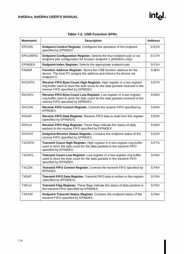
8x930Ax, 8x930Hx USER’S MANUAL
Table 7-2. USB Function SFRs
Mnemonic Description Address
EPCON Endpoint Control Register. Configures the operation of the endpoint specified by EPINDEX.
S:E1H
EPCONFIG Endpoint Configuration Register. Selects the four-endpoint pair or six-endpoint pair configuration for function endpoint 1 (8X930Ax only).
S:C7H
EPINDEX Endpoint Index Register. Selects the appropriate endpoint pair. S:F1H
FADDR Function Address Register. Stores the USB function address for the device. The host PC assigns the address and informs the device via endpoint 0.
S:8FH
RXCNTH Receive FIFO Byte-Count High Register. High register in a two-register ring buffer used to store the byte count for the data packets received in the receive FIFO specified by EPINDEX.
S:E7H
RXCNTL Receive FIFO Byte-Count Low Register. Low register in a two-register ring buffer used to store the byte count for the data packets received in the receive FIFO specified by EPINDEX.
S:E6H
RXCON Receive FIFO Control Register. Controls the receive FIFO specified by EPINDEX.
S:E4H
RXDAT Receive FIFO Data Register. Receive FIFO data is read from this register (specified by EPINDEX).
S:E3H
RXFLG Receive FIFO Flag Register. These flags indicate the status of data packets in the receive FIFO specified by EPINDEX.
S:E5H
RXSTAT Endpoint Receive Status Register. Contains the endpoint status of the receive FIFO specified by EPINDEX.
S:E2H
TXCNTH Transmit Count High Register. High register in a two-register ring buffer used to store the byte count for the data packets in the transmit FIFO specified by EPINDEX.
S:F7H
TXCNTL Transmit Count Low Register. Low register in a two-register ring buffer used to store the byte count for the data packets in the transmit FIFO specified by EPINDEX.
S:F6H
TXCON Transmit FIFO Control Register. Controls the transmit FIFO specified by EPINDEX.
S:F4H
TXDAT Transmit FIFO Data Register. Transmit FIFO data is written to this register (specified by EPINDEX).
S:F3H
TXFLG Transmit Flag Register. These flags indicate the status of data packets in the transmit FIFO specified by EPINDEX.
S:F5H
TXSTAT Endpoint Transmit Status Register. Contains the endpoint status of the transmit FIFO specified by EPINDEX.
S:FAH
7-4

USB FUNCTION
EPCONFIG† Address: S:C7HReset State: xxxx xxx0B
Endpoint Configuration Register. Selects the six-endpoint pair option or four-endpoint pair option as the 8x930Ax function endpoint pair configuration.
7 0
— — — — — — — SIXEPPEN
Bit Number
Bit Mnemonic Function
7:1 — Reserved:
Write zeroes to these bits.
0 SIXEPPEN Six-endpoint pair enable:††
Set this bit to select the six-endpoint pair (6EPP) configuration, which provides the following FIFO sizes (bytes).
EPINDEX FFSZ1:0
0xxx x000 xx0xxx x001 00†††
0xxx x010 xx0xxx x011 xx0xxx x100 xx0xxx x101 xx
TransmitFIFO
1625632323216
ReceiveFIFO
1625632323216
Clear this bit to select the four-endpoint pair (4EPP) configuration, which provides the following FIFO sizes (bytes).
EPINDEX FFSZ1:0
0xxx xx00 xx0xxx xx01 00
011011
0xxx xx10 xx0xxx xx11 xx
TransmitFIFO
162565121024
01616
ReceiveFIFO
162565120
10241616
† 8x930Ax only. Early sample devices did not have this SFR.†† Select the endpoint configuration during initialization and do not change during program execution.††† When using function endpoint 1 in the six-endpoint pair configuration, clear the FFSZ1:0 bits in
TXCON to select the 256-byte size for the transmit and receive FIFOs.
Figure 7-1. EPCONFIG: Endpoint Conf iguration Register
7-5

8x930Ax, 8x930Hx USER’S MANUAL
EPINDEX Address: S:F1HReset State: 1xxx x000B
Endpoint Index Register. This register identifies the endpoint pair. Its contents select the transmit and receive FIFO pair and serve as an index to endpoint-specific SFRs.
7 0
8X930Hx HORF — — — — — EPINX1 EPINX0
7 0
8X930Ax4 EPP
— — — — — — EPINX1 EPINX0
7 0
8X930Ax 6 EPP
— — — — — EPINX2 EPINX1 EPINX0
BitNumber
BitMnemonic Function
7 HORF
(8X930Hx)
Hub/function Bit:
1 = Hub. Selects USB hub FIFOs and SFRs.0 = Function. Selects USB function FIFOs and SFRs.
—(8X930Ax)
Reserved:
Although the reset state for this bit is “1”, always write a zero to this bit for 8X930Ax applications.
6:3 — Reserved:
Write zeros to these bits.
2 —
8X930Hx or8X930Ax(4 EPP)
Reserved:
Write a zero to this bit. 8x930Hx
1:0 EPINX1:0
8X930Hxor
8X930Ax(4 EPP)
Endpoint Index:
EPINDEX†
0xxx xx00 Function Endpoint 00xxx xx01 Function Endpoint 10xxx xx10 Function Endpoint 20xxx xx11 Function Endpoint 3
EPINDEX† (8x930Hx only)1xxx xx00 Hub Endpoint 01xxx xx01 Hub Endpoint 1
2:0 EPINX2:0
8X930Ax (6 EPP)
Endpoint Index:
EPINDEX†
0xxx x000 Function Endpoint 00xxx x001 Function Endpoint 10xxx x010 Function Endpoint 20xxx x011 Function Endpoint 30xxx x100 Function Endpoint 40xxx x101 Function Endpoint 5
† The EPINDEX register identifies the endpoint pair and selects the associated transmit and receive FIFO pair. The value in this register plus SFR addresses select the associated bank of endpoint-indexed SFRs (TXDAT, TXCON, TXFLG, TXCNTH/L, RXDAT, RXCON, RXFLG, RXCNTH/L, EPCON, TXSTAT, and RXSTAT).
Figure 7-2. EPINDEX: Endpoint Index Register
7-6

USB FUNCTION
EPCON(Endpoint-indexed)
Address: S:E1HReset State: Endpoint 0 0011 0101B
Function Endpoints 1, 2, 3 0001 0000B
Endpoint Control Register. This SFR configures the operation of the endpoint specified by EPINDEX.
7 0
RXSTL TXSTL CTLEP RXSPM RXIE RXEPEN TXOE TXEPEN
Bit Number
Bit Mnemonic Function
7 RXSTL Stall Receive Endpoint:
Set this bit to stall the receive endpoint. Clear this bit only when the host has intervened through commands sent down endpoint 0. When this bit is set and RXSETUP is clear, the receive endpoint will respond with a STALL handshake to a valid OUT token. When this bit is set and RXSETUP is set, the receive endpoint will NAK. This bit does not affect the reception of SETUP tokens by a control endpoint.
6 TXSTL Stall Transmit Endpoint:
Set this bit to stall the transmit endpoint. This bit should be cleared only when the host has intervened through commands sent down endpoint 0. When this bit is set and RXSETUP is clear, the receive endpoint will respond with a STALL handshake to a valid IN token. When this bit is set and RXSETUP is set, the receive endpoint will NAK
5 CTLEP Control Endpoint:†Set this bit to configure the endpoint as a control endpoint. Only control endpoints are capable of receiving SETUP tokens.
4 RXSPM Receive Single Packet Mode:†
Set this bit to configure the receive endpoint for single data packet operation. When enabled, only a single data packet is allowed to reside in the receive FIFO. NOTE: For control endpoints (CTLEP=1), this bit should be set for single
packet mode operation as the recommended firmware model. However, it is possible to have a control endpoint configured in dual packet mode as long as the firmware handles the endpoint correctly.
3 RXIE Receive Input Enable:
Set this bit to enable data from the USB to be written into the receive FIFO. If cleared, the endpoint will not write the received data into the receive FIFO and at the end of reception, but will return a NAK handshake on a valid OUT token if the RXSTL bit is not set.This bit does not affect a valid SETUP token. A valid SETUP token and packet overrides this bit if it is cleared, and place the receive data in the FIFO.
† For hub endpoint 0 (EPINDEX = 1000 0000, 8x930Hx only), bits 5 and 4 are hard-wired to ‘1’ since hub endpoint 0 is always a control endpoint.
Figure 7-3. EPCON: Endpoint Cont rol Register
7-7

8x930Ax, 8x930Hx USER’S MANUAL
2 RXEPEN Receive Endpoint Enable:
Set this bit to enable the receive endpoint. When disabled, the endpoint does not respond to a valid OUT or SETUP token. This bit is hardware read-only and has the highest priority among RXIE and RXSTL. Note that endpoint 0 is enabled for reception upon reset.
1 TXOE Transmit Output Enable:
This bit is used to enable the data in TXDAT to be transmitted. If cleared, the endpoint returns a NAK handshake to a valid IN token if the TXSTL bit is not set.
0 TXEPEN Transmit Endpoint Enable:
This bit is used to enable the transmit endpoint. When disabled, the endpoint does not respond to a valid IN token. This bit is hardware read only. Note that endpoint 0 is enabled for transmission upon reset.
EPCON (Continued)(Endpoint-indexed)
Address: S:E1HReset State: Endpoint 0 0011 0101B
Function Endpoints 1, 2, 3 0001 0000B
Endpoint Control Register. This SFR configures the operation of the endpoint specified by EPINDEX.
7 0
RXSTL TXSTL CTLEP RXSPM RXIE RXEPEN TXOE TXEPEN
Bit Number
Bit Mnemonic Function
† For hub endpoint 0 (EPINDEX = 1000 0000, 8x930Hx only), bits 5 and 4 are hard-wired to ‘1’ since hub endpoint 0 is always a control endpoint.
Figure 7-3. EPCON: Endpoint Control Register (Continued)
7-8

USB FUNCTION
TXSTAT (Endpoint-indexed)
Address: S:F2HReset State: 0000 0000B
Endpoint Transmit Status Register. Contains the current endpoint status of the transmit FIFO specified by EPINDEX.
7 0
TXSEQ — — TXFLUSH TXSOVW TXVOID TXERR TXACK
Bit Number
Bit Mnemonic Function
7 TXSEQ Transmitter’s Current Sequence Bit (read, conditional write): †
This bit will be transmitted in the next PID and toggled on a valid ACK handshake. This bit is toggled by hardware on a valid SETUP token. This bit can be written by firmware if the TXSOVW bit is set when written together with the new TXSEQ value.
6:5 — Reserved:
Write zeros to these bits.
4 TXFLUSH Transmit FIFO Packet Flushed (read-only):
When set, this bit indicates that hardware flushed a stale ISO data packet from the transmit FIFO due to a TXFIF1:0 = 11 at SOF. To guard against a missed IN token in ISO mode, if, with TXFIF1:0 = 11, no IN token is received for the current endpoint, hardware automatically flushes the oldest packet and decrements the TXFIF1:0 value.
3 TXSOVW Transmit Data Sequence Overwrite Bit: †
Write a ‘1’ to this bit to allow the value of the TXSEQ bit to be overwritten. Writing a ‘0’ to this bit has no effect on TXSEQ. This bit always returns ‘0’ when read. ††
2 TXVOID Transmit Void (read-only): †††
A void condition has occurred in response to a valid IN token. Transmit void is closely associated with the NAK/STALL handshake returned by the function after a valid IN token, due to the conditions that cause the transmit FIFO to be unenabled or not ready to transmit.
Use this bit to check any NAK/STALL handshake returned by the function.
This bit does not affect the FTXDx, TXERR or TXACK bits. This bit is updated by hardware at the end of a non-isochronous transaction in response to a valid IN token. For isochronous transactions, this bit is not updated until the next SOF.
† Under normal operation, this bit should not be modified by the user.†† The SIE will handle all sequence bit tracking. This bit should only be used when initializing a new
configuration or interface.††† For additional information on the operation of these bits see Appendix D, “Data Flow Model.”
Figure 7-4. TXSTAT: Transmit FIFO Status Register
7-9
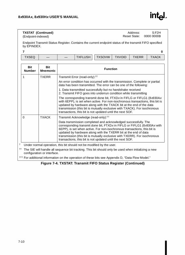
8x930Ax, 8x930Hx USER’S MANUAL
1 TXERR Transmit Error (read-only):††
An error condition has occurred with the transmission. Complete or partial data has been transmitted. The error can be one of the following:
1. Data transmitted successfully but no handshake received2. Transmit FIFO goes into underrun condition while transmitting
The corresponding transmit done bit, FTXDx in FIFLG or FIFLG1 (8x930Ax with 6EPP), is set when active. For non-isochronous transactions, this bit is updated by hardware along with the TXACK bit at the end of the data transmission (this bit is mutually exclusive with TXACK). For isochronous transactions, this bit is not updated until the next SOF.
0 TXACK Transmit Acknowledge (read-only):††
Data transmission completed and acknowledged successfully. The corresponding transmit done bit, FTXDx in FIFLG or FIFLG1 (8x930Ax with 6EPP), is set when active. For non-isochronous transactions, this bit is updated by hardware along with the TXERR bit at the end of data transmission (this bit is mutually exclusive with TXERR). For isochronous transactions, this bit is not updated until the next SOF.
TXSTAT (Continued) (Endpoint-indexed)
Address: S:F2HReset State: 0000 0000B
Endpoint Transmit Status Register. Contains the current endpoint status of the transmit FIFO specified by EPINDEX.
7 0
TXSEQ — — TXFLUSH TXSOVW TXVOID TXERR TXACK
Bit Number
Bit Mnemonic Function
† Under normal operation, this bit should not be modified by the user.†† The SIE will handle all sequence bit tracking. This bit should only be used when initializing a new
configuration or interface.††† For additional information on the operation of these bits see Appendix D, “Data Flow Model.”
Figure 7-4. TXSTAT: Transmit FIFO Status Register (Continued)
7-10

USB FUNCTION
RXSTAT (Endpoint-indexed)
Address: S:E2H Reset State: 0000 0000B
Endpoint Receive Status Register. Contains the current endpoint status of the receive FIFO specified by EPINDEX. (Endpoint-indexed SFR)
7 0
RXSEQ RXSETUP STOVW EDOVW RXSOVW RXVOID RXERR RXACK
Bit Number
Bit Mnemonic Function
7 RXSEQ Receiver Endpoint Sequence Bit (read, conditional write): †
This bit will be toggled on completion of an ACK handshake in response to an OUT token. This bit will be set (or cleared) by hardware after reception of a SETUP token.
This bit can be written by firmware if the RXSOVW bit is set when written along with the new RXSEQ value.NOTE: Always verify this bit after writing to ensure that there is no conflict
with hardware, which could occur if a new SETUP token is received.
6 RXSETUP Received Setup Token:
This bit is set by hardware when a valid SETUP token has been received. When set, this bit causes received IN or OUT tokens to be NAKed until the bit is cleared to allow proper data management for the transmit and receive FIFOs from the previous transaction.
IN or OUT tokens are NAKed even if the endpoint is stalled (RXSTL or TXSTL) to allow a control transaction to clear a stalled endpoint.
Clear this bit upon detection of a SETUP token after the firmware is ready to complete the status stage of a control transaction.
5 STOVW Start Overwrite Flag (read-only):
Set by hardware upon receipt of a SETUP token for any control endpoint to indicate that the receive FIFO is being overwritten with new SETUP data. When set, the FIFO state (FIF and read pointer) resets and is locked for this endpoint until EDOVW is set. This prevents a prior, ongoing firmware read from corrupting the read pointer as the receive FIFO is being cleared and new data is being written into it. This bit is cleared by hardware at the end of handshake phase transmission of the setup stage.
This bit is used only for control endpoints.
† Under normal operation, this bit should not be modified by the user.†† For additional information on the operation of these bits see Appendix D, “Data Flow Model.”††† The SIE will handle all sequence bit tracking. This bit should be used only when initializing a new
configuration or interface.
Figure 7-5. RXSTAT: Receive FIFO Status Register
7-11

8x930Ax, 8x930Hx USER’S MANUAL
4 EDOVW End Overwrite Flag:† This flag is set by hardware during the handshake phase of a SETUP stage. It is set after every SETUP packet is received and must be cleared prior to reading the contents of the FIFO. When set, the FIFO state (FIF and read pointer) remains locked for this endpoint until this bit is cleared. This prevents a prior, ongoing firmware read from corrupting the read pointer after the new data has been written into the receive FIFO.
This bit is only used for control endpoints.NOTE: Make sure the EDOVW bit is cleared prior to reading the contents
of the FIFO.
3 RXSOVW Receive Data Sequence Overwrite Bit: †
Write a ‘1’ to this bit to allow the value of the RXSEQ bit to be overwritten. Writing a ‘0’ to this bit has no effect on RXSEQ. This bit always returns ‘0’ when read. †††
2 RXVOID Receive Void Condition (read-only):††
This bit is set when no valid data is received in response to a SETUP or OUT token due to one of the following conditions:
1. The receive FIFO is still locked
2. The EPCON register’s RXSTL bit is set
This bit is set and cleared by hardware. For non-isochronous transactions, this bit is updated by hardware at the end of the transaction in response to a valid OUT token. For isochronous transactions, it is not updated until the next SOF.
RXSTAT (Continued)(Endpoint-indexed)
Address: S:E2H Reset State: 0000 0000B
Endpoint Receive Status Register. Contains the current endpoint status of the receive FIFO specified by EPINDEX. (Endpoint-indexed SFR)
7 0
RXSEQ RXSETUP STOVW EDOVW RXSOVW RXVOID RXERR RXACK
Bit Number
Bit Mnemonic Function
† Under normal operation, this bit should not be modified by the user.†† For additional information on the operation of these bits see Appendix D, “Data Flow Model.”††† The SIE will handle all sequence bit tracking. This bit should be used only when initializing a new
configuration or interface.
Figure 7-5. RXSTAT: Receive FIFO Status Register (Continued)
7-12

USB FUNCTION
1 RXERR Receive Error (read-only):††
Set when an error condition has occurred with the reception. Complete or partial data has been written into the receive FIFO. No handshake is returned. The error can be one of the following conditions:
1. Data failed CRC check.
2. Bit stuffing error.
3. A receive FIFO goes into overrun or underrun condition while receiving.
This bit is updated by hardware at the end of a valid SETUP or OUT token transaction (non-isochronous) or at the next SOF on each valid OUT token transaction (isochronous).
The corresponding FRXDx bit of FIFLG or FIFLG1 (8x930Ax with 6EPP) is set when active. This bit is updated with the RXACK bit at the end of data reception and is mutually exclusive with RXACK.
0 RXACK Receive Acknowledged (read-only):††
This bit is set when data is received completely into a receive FIFO and an ACK handshake is sent. This read-only bit is updated by hardware at the end of a valid SETUP or OUT token transaction (non-isochronous) or at the next SOF on each valid OUT token transaction (isochronous).
The corresponding FRXDx bit of FIFLG or FIFLG1 (8x930Ax with 6EPP) is set when active. This bit is updated with the RXERR bit at the end of data reception and is mutually exclusive with RXERR.
RXSTAT (Continued)(Endpoint-indexed)
Address: S:E2H Reset State: 0000 0000B
Endpoint Receive Status Register. Contains the current endpoint status of the receive FIFO specified by EPINDEX. (Endpoint-indexed SFR)
7 0
RXSEQ RXSETUP STOVW EDOVW RXSOVW RXVOID RXERR RXACK
Bit Number
Bit Mnemonic Function
† Under normal operation, this bit should not be modified by the user.†† For additional information on the operation of these bits see Appendix D, “Data Flow Model.”††† The SIE will handle all sequence bit tracking. This bit should be used only when initializing a new
configuration or interface.
Figure 7-5. RXSTAT: Receive FIFO Status Register (Continued)
7-13
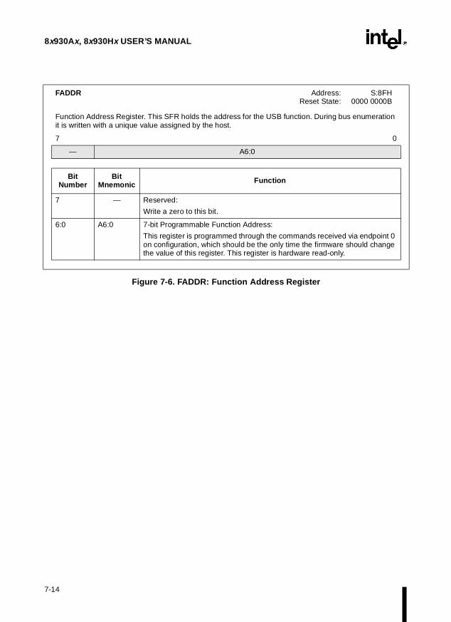
8x930Ax, 8x930Hx USER’S MANUAL
Figure 7-6. FADDR: Function Address Register
FADDR Address: S:8FHReset State: 0000 0000B
Function Address Register. This SFR holds the address for the USB function. During bus enumeration it is written with a unique value assigned by the host.
7 0
— A6:0
Bit Number
Bit Mnemonic Function
7 — Reserved:
Write a zero to this bit.
6:0 A6:0 7-bit Programmable Function Address:
This register is programmed through the commands received via endpoint 0 on configuration, which should be the only time the firmware should change the value of this register. This register is hardware read-only.
7-14

USB FUNCTION
smitthe
ciatedave two
t,The
7.2 TRANSMIT FIFOS
The 8x930 has a transmit FIFO for each function endpoint pair. In this manual, the term “tranFIFO” refers to the transmit FIFO associated with the current endpoint pair specified by EPINDEX register. 8x930 FIFOs are listed in Table 2-5 and Table 2-6 on page 2-13.
7.2.1 Transmit FIFO Overview
The transmit FIFOs are circulating data buffers with the following features:
• support for up to two separate data sets of variable sizes†
• a byte count register to store the number of bytes in the data sets
• protection against overwriting data in a full FIFO
• capability to retransmit the current data set
All transmit FIFOs have the same architecture (Figure 7-7). The transmit FIFO and its assologic can manage up to two data sets, data set 0 (ds0) and data set 1 (ds1). The ability to hdata sets in the FIFO supports back-to-back transmissions.
Figure 7-7. Transmit FIFO Outline
The CPU writes to the FIFO location specified by the write pointer, which automatically incre-ments by one after a write. The read marker points to the first byte of data written to a data seand the read pointer points to the next FIFO location to be read by the function interface. read pointer automatically increments by one after a read.
† When operating in dual packet mode, the maximum packet size should be at most half the FIFO size to ensure that both packets will simultaneously fit in the FIFO (see the Endpoint description in the Universal Serial Bus Specification).
A4258-02
Write Pointer
Data Set 0
Data Set 1
Read Marker
Read Pointer
REVRP ADVRM
FIU Reads FIFO
8X930 CPU Writes to FIFO
TXCNTH
TXCNTL
To USB Interface
From CPU
Byte Count Registers
7-15
8x930Ax, 8x930Hx USER’S MANUAL
n of theted, theface torsal cand by
n of theguresf-
range-
twosets as-
o
When a good transmission is completed, the read marker can be advanced to the positioread pointer to set up for reading the next data set. When a bad transmission is compleread pointer can be reversed to the position of the read marker to enable the function interre-read the last data set for retransmission. The read marker advance and read pointer revebe accomplished two ways: explicitly by firmware or automatically by hardware, as specifiebits in the transmit FIFO control register (TXCON).
7.2.2 Transmit FIFO Registers
There are five registers directly involved in the operation of the transmit FIFOs:
• TXDAT, the transmit FIFO data register
• TXCNTH and TXCNTL, the transmit FIFO byte count registers referred to jointly as TXCNT
• TXCON, the transmit FIFO control register
• TXFLG, the transmit FIFO flag register
These registers are endpoint indexed, i.e., they are used as a set to control the operatiotransmit FIFO associated with the current endpoint specified by the EPINDEX register. Fi7-8 through 7-11 beginning on page 7-18 describe the transmit FIFO registers and provide bit deinitions.
7.2.3 Transmit Data Register (TXDAT)
Bytes are written to the transmit FIFO via TXDAT, the transmit FIFO data register (Figure 7-8on page 7-18).
7.2.4 Transmit Byte Count Registers (TXCNTL/TXCNTH)
The format of the transmit byte count register depends on the endpoint. For endpoint 1, registersTXCNTH and TXCNTL form a two-register, ten-bit ring buffer. For endpoints 0, 2, and 3 (andfor the 8x930Ax, endpoints 4 and 5), TXCNTL is used alone as a five-bit ring buffer. These for-mats are shown in Figure 7-9 on page 7-19. The term TXCNT refers to either of these arments.
The transmit FIFO byte count register (TXCNT) stores the number of bytes in either of thedata sets, data set 0 (ds0) and data set 1 (ds1). The FIFO logic for maintaining the data sumes that data is written to the FIFO in the following sequence:
1. The CPU first writes data bytes to TXDAT.
2. The CPU writes the number of bytes that were written to TXDAT to the byte count register TXCNT. TXCNT must be written after the write to TXDAT to guarantee data integrity. For function endpoint 1, TXCNTL should be written after TXCNTH. Writing tTXCNTH does not affect the TXFIF bits, however writing to TXCNTHL does set the associated TXFIF bits.
7-16

USB FUNCTION
e set.
the leftet,next. In this
ite to
set
er is
NOTETXCNTH does not need to be written if it is always 00H, as the reset value is 00H. However, if TXCNTH is not 00H, it should always be written even though the value does not change from the previous cycle; this is because the byte count registers are 2-byte circular buffers and not “static” registers.
For all endpoints except function endpoint 1, TXCNTH is not available and TXCNTL only contains BC4:0. Bits 7:5 are reserved in this case and should always be written with ‘0’.
The function interface reads the byte count register to determine the number of bytes in th
7.2.5 Transmit Data Set Management
Two read-only data set index bits, FIF1:0 in the TXFLG register, indicate which data sets(ds0and/or ds1) have been written into the FIFO and are armed (ready for transmission). See side of Table 7-3. FIFx = 1 indicates that data set x has been written and is armed. Following resFIF1:0 = 00, signifying an empty FIFO. FIF1:0 also determine which data set is written Note that FIF0 specifies the next data set to be written, except for the case of FIF1:0 = 11.case further writes to TXDAT or TXCNT are ignored.
NOTETo simplify firmware development, it is recommended that you utilize control endpoints in single-packet mode only.
Two events cause the data set index bits to be updated:
• A new data set is written to the FIFO: the 8x930 writes bytes to the FIFO via TXDAT and writes the number of bytes to TXCNT. The data set index bits are updated after the wrTXCNT. This process is illustrated in Table 7-3.
• A data set in the FIFO is successfully transmitted: the function interface reads a data from the FIFO, and when a good transmission is acknowledged, the read marker is advanced to the read pointer. The data set index bits are updated after the read markadvanced. Note that in ISO mode, this happens at the next SOF.
Table 7-3. Writing to the Byte Count Register
FIF1:0 Data Sets Written Set for Next Write
to TXCNTWrite bytesto TXDAT.
FIF1:0ds1 ds0
0 0 No No (Empty) ds0 —> Write bytecount toTXCNT
—> 0 1
0 1 No Yes (1 set) ds1 1 1
1 0 Yes No (1 set) ds0 1 1
1 1 Yes Yes (2 sets) Write ignored 1 1
7-17

8x930Ax, 8x930Hx USER’S MANUAL
it, the
Table 7-4 summarizes how the actions following a transmission depend on the TXISO bATM bit, the TXACK bit, and the TXERR bit.NOTEFor normal operation, set the ATM bit in TXCON. Hardware will automatically control the read pointer and read marker, and track the TXFIF bits.
Figure 7-8. TXDAT: Transmit FIFO Data Register
Table 7-4. Truth Table for Transmit FIFO Management
TXISO(TXCON.3)
ATM(TXCON.2)
TXERR(TXSTAT.1)
TXACK(TXSTAT.0) Action at End of Transfer Cycle
X X 0 0 No operation.
X 0 0 1 Read marker, read pointer, and TXFIF bits remain unchanged. Managed by firmware.
X 0 1 0 Read marker, read pointer, and TXFIF bits remain unchanged. Managed by firmware.
0 1 0 1 Read marker advanced automatically.The TXFIF bit for the corresponding data set is cleared.
0 1 1 0 Read pointer reversed automatically. The TXFIF bit for the corresponding data set remains unchanged.
1 1 X X Read marker advanced automatically.The TXFIF bit for the corresponding data set is cleared at the SOF.
TXDAT (Endpoint-indexed)†
Address: S:F3HReset State: xxxx xxxxB
USB Transmit FIFO Data Register. Data to be transmitted by the FIFO specified by EPINDEX is first written to this register.
7 0
Transmit Data Byte
Bit Number
Bit Mnemonic Function
7:0 TXDAT.7:0 Transmit Data Byte (write-only):
To write data to the transmit FIFO, write to this register. The write pointer is incremented automatically after a write.
† For hub endpoint 1, TXDAT is used in a different manner. See Figure 8-6 on page 8-12.
7-18

USB FUNCTION
Figure 7-9. TXCNTH/TXCNTL Transmit FIFO Byte Count Registers
NOTETo send a status stage after a control write or no data control command or a null packet, write 0 to TXCNT.
TXCNTH,TXCNTL(Endpoint-indexed)
Address: S:F7HS:F6H
Reset States: Endpoint 1 TXCNTH xxxx xx00BTXCNTL 0000 0000B
OtherEndpoints† TXCNTL xxx0 0000B
Transmit FIFO Byte-count High and Low Registers. High and low register in a two-register ring buffer used to store the byte count for the data packets in the transmit FIFO specified by EPINDEX. Note that TXCNTH exists only for function endpoint 1 and is unavailable for all other endpoints.
15 (TXCNTH) Endpoint 1 8
— — — — — — BC9 BC8
7 (TXCNTL) 0
BC7 BC6 BC5 BC4 BC3 BC2 BC1 BC0
7 (TXCNTL) Other Endpoints 0
— — — BC4 BC3 BC2 BC1 BC0
Bit Number
Bit Mnemonic Function
Function Endpoint 1
15:10 — Reserved.
Write zeros to these bits.
9:0 BC9:0 Transmit Byte Count. (write, conditional read††)Ten-bit, ring buffer. Stores transmit byte count (TXCNT). Implemented for function endpoint 1 only.
Other Endpoints†
7:0 — Reserved.
Write zeros to these bits.
4:0 BC4:0 Transmit Byte Count. (write, conditional read††)Five-bit, ring buffer. Stores transmit byte count (TXCNT) for endpoints 0, 2, and 3.
† Other endpoints = Hub endpoint 0; function endpoints 0, 3:2 or 0, 5:2 (6EPP option, 8x930Ax only). Byte count registers are not implemented for hub endpoint 1.
†† Read these bits only if TXFIF1:0 = 0; otherwise underrun errors may occur.
7-19

8x930Ax, 8x930Hx USER’S MANUAL
TXCON(Endpoint-indexed)
Address: S:F4HReset State: Function Endpoint 1 000x 0100B
Other Endpoints† 0xxx 0100B
USB Transmit FIFO Control Register. Controls the transmit FIFO specified by EPINDEX.
7 0
Function Endpoint 1
TXCLR FFSZ1 FFSZ0 — TXISO ATM ADVRM REVRP
7 0
Other Endpoints †
TXCLR — — — TXISO ATM ADVRM REVRP
BitNumber
BitMnemonic Function
7 TXCLR Transmit Clear:
Setting this bit flushes the transmit FIFO, resets all the read/write pointers and markers, sets the EMPTY bit in TXFLG, and clears all other bits in TXFLG. After the flush, hardware clears this bit. Setting this bit does not affect the ATM, TXISO, and FFSZ bits, or the TXSEQ bit in the TXSTAT register.
6:5 FFSZ1:0
Function Endpoint 1 only
FIFO Size:
For function endpoint 1 only (EPINDEX = 0000 0001B), these bits select the sizes of both the transmit and receive FIFOs. (There are no FFSZ bits in the corresponding RXCON.) These bits are not reset when the TXCLR bit is set in the TXCON register.
FFSZ1:0 Transmit Size Receive Size
00 256 25601 512 51210 1024 011 0 1024
—
Other End-points †
Reserved:
Values read from this bit are indeterminate. Write zero to this bit.
4 — Reserved:
Values read from this bit are indeterminate. Write zero to this bit.
3 TXISO Transmit Isochronous Data:
Firmware sets this bit to indicate that the transmit FIFO contains isochronous data. The FIU uses this bit to set up the handshake protocol at the end of a transmission. This bit is not reset when TXCLR is set and must be cleared by firmware.
† Other endpoints = Hub endpoint 0; function endpoints 0, 3:2 or 0, 5:2 (for 6EPP option, 8x930Ax only).
†† ATM mode is recommended. ADVRM and REVRP, which control the read marker and read pointer when ATM = 0, are used for test purposes,
Figure 7-10. TXCON: Transmit FIFO Control Register
7-20

USB FUNCTION
2 ATM Automatic Transmit Management:
Setting this bit (the default value) causes the read pointer and read marker to be adjusted automatically as indicated:
TXISOTX Status Read Pointer Read Marker
X ACK Unchanged Advanced (1)0 NAK Reversed (2) Unchanged1 NAK Unchanged Advanced (1)
1. to origin of next data set 2. to origin of the data set last read
This bit should always be set, except for test purposes. Setting this bit disables ADVRM and REVRP. This is a sticky bit that is not reset when TXCLR is set, but can be set and cleared by firmware. Hardware neither clears nor sets this bit.
1 ADVRM Advance Read Marker Control (non-ATM mode only)††:
Setting this bit prepares for the next packet transmission by advancing the read marker to the origin of the next data packet (the position of the read pointer). Hardware clears this bit after the read marker is advanced. This bit is effective only when the REVRP, ATM, and TXCLR bits are all clear.
0 REVRP Reverse Read Pointer Control (non-ATM mode only)††:
In the case of a bad transmission, the same data stack may need to be available for retransmit. Setting this bit reverses the read pointer to point to the origin of the last data set (the position of the read marker) so that the FIU can reread the last set for retransmission. Hardware clears this bit after the read pointer is reversed. This bit is effective only when the ADVRM, ATM, and TXCLR bits are all clear.
TXCON (Continued)(Endpoint-indexed)
Address: S:F4HReset State: Function Endpoint 1 000x 0100B
Other Endpoints† 0xxx 0100B
USB Transmit FIFO Control Register. Controls the transmit FIFO specified by EPINDEX.
7 0
Function Endpoint 1
TXCLR FFSZ1 FFSZ0 — TXISO ATM ADVRM REVRP
7 0
Other Endpoints †
TXCLR — — — TXISO ATM ADVRM REVRP
BitNumber
BitMnemonic Function
† Other endpoints = Hub endpoint 0; function endpoints 0, 3:2 or 0, 5:2 (for 6EPP option, 8x930Ax only).
†† ATM mode is recommended. ADVRM and REVRP, which control the read marker and read pointer when ATM = 0, are used for test purposes,
Figure 7-10. TXCON: Transmit FIFO Control Register (Continued)
7-21

8x930Ax, 8x930Hx USER’S MANUAL
TXFLG(Endpoint-indexed)
Address: S:F5HReset State: 00xx 1000B
Transmit FIFO Flag Register. These flags indicate the status of data packets in the transmit FIFO specified by EPINDEX.
7 0
TXFIF1 TXFIF0 — — TXEMP TXFULL TXURF TXOVF
Bit Number
Bit Mnemonic Function
7:6 TXFIF1:0 FIFO Index Flags (read-only):
These flags indicate which data sets are present in the transmit FIFO. The FIF bits are set in sequence after each write to TXCNT to reflect the addition of a data set. Likewise, TXFIF1 and TXFIF0 are cleared in sequence after each advance of the read marker to indicate that the set is effectively discarded. The bit is cleared whether the read marker is advanced by firmware (setting ADVRM) or automatically by hardware (ATM = 1). The next-state table for the TXFIF bits is shown below:
TXFIF1:0 Operation Flag Next TXFIF1:0 Next Flag
00 Wr TXCNT X 01 Unchanged01 Wr TXCNT X 11 Unchanged10 Wr TXCNT X 11 Unchanged11 Wr TXCNT X 11 TXOVF = 1
00 Adv RM X 00 Unchanged01 Adv RM X 00 Unchanged11 Adv RM X 10/01 Unchanged10 Adv RM X 00 Unchanged
XX Rev RP X Unchanged Unchanged
In ISO mode, TXOVF, TXURF, and TXFIF are handled using the following rule: Firmware events cause status change immediately, while USB events cause status change only at SOF. TXFIF is “incremented” by firmware and “decremented” by the USB.Therefore, writes to TXCNT “increment” TXFIF immediately. However, a successful USB transaction any time within a frame “decrements” TXFIF only at SOF. You must check the TXFIF flags before and after writes to the transmit FIFO and TXCNT for traceability. See the TXFLUSH bit in TXSTST.NOTE: To simplify firmware development, configure control endpoints in
single-packet mode.
5:4 — Reserved:
Values read from these bits are indeterminate. Write zeros to these bits.
3 TXEMP Transmit FIFO Empty Flag (read-only):
Hardware sets this bit when the write pointer has not rolled over and is at the same location as the read pointer. Hardware clears this bit when the pointers are at different locations.
Regardless of ISO or non-ISO mode, this bit always tracks the current transmit FIFO status.
† When set, all transmissions are NAKed.
Figure 7-11. TXFLG: Transmit FIFO Flag Register
7-22
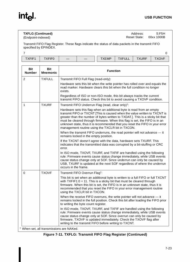
USB FUNCTION
2 TXFULL Transmit FIFO Full Flag (read-only):
Hardware sets this bit when the write pointer has rolled over and equals the read marker. Hardware clears this bit when the full condition no longer exists.
Regardless of ISO or non-ISO mode, this bit always tracks the current transmit FIFO status. Check this bit to avoid causing a TXOVF condition.
1 TXURF Transmit FIFO Underrun Flag (read, clear only)†:
Hardware sets this flag when an additional byte is read from an empty transmit FIFO or TXCNT [This is caused when the value written to TXCNT is greater than the number of bytes written to TXDAT.]. This is a sticky bit that must be cleared through firmware. When this flag is set, the FIFO is in an unknown state, thus it is recommended that you reset the FIFO in your error management routine using the TXCLR bit in TXCON.
When the transmit FIFO underruns, the read pointer will not advance — it remains locked in the empty position.
If the TXCNT doesn’t agree with the data, hardware sets TXURF. This indicates that the transmitted data was corrupted by a bit-stuffing or CRC error.
In ISO mode, TXOVF, TXURF, and TXFIF are handled using the following rule: Firmware events cause status change immediately, while USB events cause status change only at SOF. Since underrun can only be caused by USB, TXURF is updated at the next SOF regardless of where the underrun occurs in the frame.
0 TXOVF Transmit FIFO Overrun Flag†:
This bit is set when an additional byte is written to a full FIFO or full TXCNT with TXFIF1:0 = 11. This is a sticky bit that must be cleared through firmware. When this bit is set, the FIFO is in an unknown state, thus it is recommended that you reset the FIFO in your error management routine using the TXCLR bit in TXCON.
When the receive FIFO overruns, the write pointer will not advance — it remains locked in the full position. Check this bit after loading the FIFO prior to writing the byte count register.
In ISO mode, TXOVF, TXURF, and TXFIF are handled using the following rule: Firmware events cause status change immediately, while USB events cause status change only at SOF. Since overrun can only be caused by firmware, TXOVF is updated immediately. Check the TXOVF flag after writing to the transmit FIFO before writing to TXCNT.
TXFLG (Continued)(Endpoint-indexed)
Address: S:F5HReset State: 00xx 1000B
Transmit FIFO Flag Register. These flags indicate the status of data packets in the transmit FIFO specified by EPINDEX.
7 0
TXFIF1 TXFIF0 — — TXEMP TXFULL TXURF TXOVF
Bit Number
Bit Mnemonic Function
† When set, all transmissions are NAKed.
Figure 7-11. TXFLG: Transmit FIFO Flag Register (Continued)
7-23
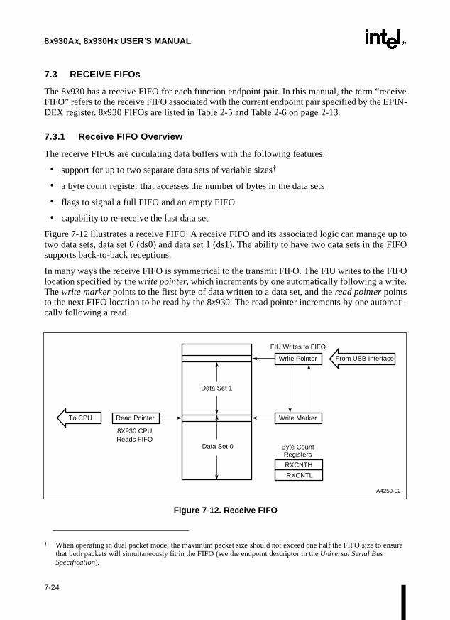
8x930Ax, 8x930Hx USER’S MANUAL
ceiveEPIN-
e up to
FIFO.
ti-
7.3 RECEIVE FIFOs
The 8x930 has a receive FIFO for each function endpoint pair. In this manual, the term “reFIFO” refers to the receive FIFO associated with the current endpoint pair specified by the DEX register. 8x930 FIFOs are listed in Table 2-5 and Table 2-6 on page 2-13.
7.3.1 Receive FIFO Overview
The receive FIFOs are circulating data buffers with the following features:
• support for up to two separate data sets of variable sizes†
• a byte count register that accesses the number of bytes in the data sets
• flags to signal a full FIFO and an empty FIFO
• capability to re-receive the last data set
Figure 7-12 illustrates a receive FIFO. A receive FIFO and its associated logic can managtwo data sets, data set 0 (ds0) and data set 1 (ds1). The ability to have two data sets in the FIFOsupports back-to-back receptions.
In many ways the receive FIFO is symmetrical to the transmit FIFO. The FIU writes to the location specified by the write pointer, which increments by one automatically following a writeThe write marker points to the first byte of data written to a data set, and the read pointer pointsto the next FIFO location to be read by the 8x930. The read pointer increments by one automacally following a read.
Figure 7-12. Receive FIFO
† When operating in dual packet mode, the maximum packet size should not exceed one half the FIFO size to ensure that both packets will simultaneously fit in the FIFO (see the endpoint descriptor in the Universal Serial Bus Specification).
A4259-02
Read Pointer
Data Set 0
Data Set 1
Write Marker
Write Pointer
FIU Writes to FIFO
8X930 CPU Reads FIFO
From USB Interface
To CPU
RXCNTH
RXCNTL
Byte Count Registers
7-24

USB FUNCTION
writeointer
ata setccom- the
ccess-
in
f the re- i-
DAT).
gisters0 tocom-
e twosets as-
IFO
When a good reception is completed, the write marker can be advanced to the position of the pointer to set up for writing the next data set. When a bad reception is completed, the write pcan be reversed to the position of the write marker to enable the FIU to rewrite the last dafter receiving the data again. The write marker advance and write pointer reversal can be aplished two ways: explicitly by firmware or automatically by hardware, as specified by bits inreceive FIFO control register.
The 8x930 should not read data from the receive FIFO before all bytes are received and sufully acknowledged because the reception may be bad.
The FIU can monitor the FIFO full flag (RXFULL bit in RXFLG) to avoid overwriting data the receive FIFO. In the single packet mode, 8x930 can monitor the FIFO empty flag (RXEMPbit in RXFLG) to avoid reading a byte when the FIFO is empty.
7.3.2 Receive FIFO Registers
There are five registers directly involved in the operation of the receive FIFOs:
• RXDAT, the receive FIFO data register
• RXCNTH and RXCNTL, the receive FIFO byte count registers referred to jointly as RXCNT
• RXCON, the receive FIFO control register
• RXFLG, the receive FIFO flag register
These registers are endpoint indexed, i.e., they are used as set to control the operation oceive FIFO associated with the current endpoint specified by the EPINDEX register. Figures7-13through 7-11 beginning on page 7-27 describe the receive FIFO registers and provide bit defintions.
7.3.2.1 Receive Data Register (RXDAT)
Received data bytes are written to the receive FIFO via the receive FIFO data register (RX
7.3.2.2 Receive Byte Count Registers (RXCNTL/RXCNTH)
The format of the receive byte count register depends on the endpoint. For endpoint 1, reRXCNTH and RXCNTL form a ten-bit ring buffer which accommodates packet sizes of 1023 bytes. For endpoints 0, 2, and 3, RXCNTL is used alone as five-bit ring buffer to acmodate packet sizes of 0 to 16 bytes. These formats are shown in Table 7-14 on page 7-28. Theterm RXCNT refers to either of these arrangements.
The receive FIFO byte count register (RXCNT) stores the number of bytes in either of thdata sets, data set 0 (ds0) and data set 1 (ds1). The FIFO logic for maintaining the data sumes that data is written to the FIFO in the following sequence:
1. The USB interface first writes the received data packet into the receive FIFO.
2. The USB interface then writes the number of bytes that were written into the receive Fto the byte count register RXCNT.
7-25

8x930Ax, 8x930Hx USER’S MANUAL
rgister.
ines
IF1:0
r) to
ARM
NOTEFor all endpoints except function endpoint 1, RXCNTH is not available and RXCNTL only contains BC4:0. Bits 7:5 are reserved in this case and will always be read as ‘0’.
The CPU reads the byte count register to determine the number of bytes in the set.
The receive byte count register has a read/write index to allow it to access the byte count for eitheof the two data sets. This is similar to the methodology used for the transmit byte count reAfter reset, the read/write index points to data set 0. Thereafter, the following logic determthe position of the read/write index:
• After a read of RXCNT, the read/write index (RXFIF) is unchanged
• After a write of RXCNT, the read/write index (RXFIF) is toggled
The position of the read/write index can also be determined from the data set index bits, F(see “Receive FIFO Data Set Management” on page 7-26).
CAUTIONDo not read RXCNT to determine if data is present in the receive FIFO. A read attempt to RXCNT during the time the receive FIFO is empty causes the RXURF flag in RXFLG to be set. Always read the RXFIF bits in RXFLG to determine if data is present in the receive FIFO. The RXFIF bits are updated after RXCNT is written (at the end of the receive operation, and at the SOF for ISO data).
7.3.3 Receive FIFO Data Set Management
As in the transmit FIFO, the receive FIFO uses a pair of bits (FIF1:0 in the RXFLG registeindicate which data sets are present in the receive FIFO (see Table 7-5).
Table 7-6 summarizes how the actions following a reception depend on the RXISO bit, thebit, and the handshake issued by the 8x930.
Table 7-5. Status of the Receive FIFO Data Sets
FIF1:0 Data Sets Written
ds1 ds0
0 0 No No (Empty)
0 1 No Yes (1 set)
1 0 Yes No (1 set)
1 1 Yes Yes (2 sets)
7-26

USB FUNCTION
NOTEFor normal operation, set the ARM bit in RXCON: hardware will automatically control the write pointer and write marker and track the RXFIF bits.
Figure 7-13. RXDAT: Receive FIFO Data Register
Table 7-6. Truth Table for Receive FIFO Management
RXISO(RXCON.3)
ARM(RXCON.2)
RXERR(RXSTAT.1)
RXACK(RXSTAT.0) Action at End of Transfer Cycle
X X 0 0 No operation.
X 0 0 1 Write marker, write pointer, and RXFIF bits remain unchanged. Managed by firmware.
X 0 1 0 Write marker, write pointer, and RXFIF bits remain unchanged. Managed by firmware.
0 1 0 1 Write marker advanced automatically. The RXFIF bit for the corresponding data set is set.
0 1 1 0 Write pointer reversed automatically.The RXFIF bit for the corresponding data set is cleared.
1 1 X X Write marker advanced automatically. If data was written to the receive FIFO, the RXFIF bit for the corresponding data set is set.
RXDAT(Endpoint-indexed)
Address: S:E3HReset: xxxx xxxxB
Receive FIFO Data Register. Receive FIFO data specified by EPINDEX is stored and read from this register.
7 0
RXDAT.7:0
Bit Number
Bit Mnemonic Function
7:0 RXDAT.7:0 To write data to the receive FIFO, the FIU writes to this register. To read data from the receive FIFO, the 8x930 reads from this register. The write pointer and read pointer are incremented automatically after a write and read, respectively.
7-27

8x930Ax, 8x930Hx USER’S MANUAL
Figure 7-14. RXCNTH/RXCNTL: Receive FIFO Byte Count Registers
CAUTIONDo not read RXCNT to determine if data is present in the receive FIFO. Always read the FIF bits in the RXFLG register. RXCNT contains random data during a receive operation. A read attempt to RXCNT during the time the receive FIFO is empty causes the RXURF flag in RXFLG to be set. Always read the FIF bits to determine if data is present in the receive FIFO. The RXFLG FIF bits are updated after RXCNT is written (at the end of the receive operation).
RXCNTH, RXCNTL(Endpoint-indexed)
Address: S:E7H S:E6H
Reset States:Endpoint 1 RXCNTH xxxx xx00B
RXCNTL 0000 0000BOther
Endpoints† RXCNTL xxx0 0000B
Receive FIFO Byte-count High and Low Registers. High and low register in a two-register ring buffer used to store the byte count for the data packets received in the receive FIFO specified by EPINDEX.
15 (RXCNT) Endpoint 1 8
— — — — — — BC9 BC8
7 (RXCNTL) 0
BC7 BC6 BC5 BC4 BC3 BC2 BC1 BC0
7 (RXCNTL) Other Endpoints† 0
— — — BC4 BC3 BC2 BC1 BC0
Bit Number
Bit Mnemonic Function
Endpoint 1
15:10 — Reserved. Write zeros to these bits.
9:0 BC9:0 Receive Byte Count.Ten-bit, ring buffer byte. Stores receive byte count (RXCNT). Implemented for function endpoint 1 only.
Other Endpoints†
7:0 — Reserved. Write zeros to these bits.
4:0 BC4:0 Receive Byte Count.Five-bit, ring buffer. Stores receive byte count (RXCNT). 3.
† Other endpoints = Hub endpoint 0; function endpoints 0, 3:2 or 0, 5:2 (6EPP option, 8x930Ax only). Byte count registers are not implemented for hub endpoint 1.
7-28

USB FUNCTION
RXCON(Endpoint-indexed)
Address: S:E4HReset State: 0x00 0100B
Receive FIFO Control Register. Controls the receive FIFO specified by EPINDEX.
7 0
RXCLR — RXWS RXFFRC RXISO ARM ADVWM REVWP
Bit Number
Bit Mnemonic Function
7 RXCLR Clear the Receive FIFO:
Set this bit to flush the entire receive FIFO. All flags in RXFLG revert to their reset states (RXEMP is set; all other flags clear). The ARM, RXISO and RXWS bits in this register and the RXSEQ bit in the RXSTAT register are not affected by this operation. Hardware clears this bit when the flush operation is completed.
6 — Reserved:
Values read from this bit are indeterminate. Write zero to this bit.
5 RXWS Receive FIFO Wait-state Read:
At the 8x930 core frequency of 12 MHz, not all instructions that access the receive FIFO are guaranteed to work due to critical paths inherent in the 8x930 architecture.While all MOV instructions from the receive FIFO are guaranteed to work at 12 MHz, arithmetic instructions (e.g., ADD, SUB, etc.) where the receive FIFO is the source and the register file the destination may not work at this speed. For applications using arithmetic instructions, set the RXWS bit to read the receive FIFO with one wait state — this will eliminate the critical path. This bit is not reset when the RXCLR bit is set.
4 RXFFRC FIFO Read Complete:†
Set this bit to release the receive FIFO when a data set read is complete. Setting this bit “clears” the RXFIF “bit” (in the RXFLG register) corresponding to the data set that was just read. Hardware clears this bit after the RXFIF bit is cleared. All data from this data set must have been read. Note that FIFO Read Complete only works if STOVW and EDOVW are cleared.
3 RXISO Isochronous Data Type:†
Set this bit to indicate that the receive FIFO is programmed to receive isochronous data and to set up the USB Interface to handle an isochronous data transfer. This bit is not reset when the RXCLR bit is set; it must be cleared by firmware.
† ARM mode is recommended. ADVWM and REVWP, which control the write marker and write pointer when ARM = 0, are used for test purposes,
Figure 7-15. RXCON: Receive FIFO Cont rol Register
7-29

8x930Ax, 8x930Hx USER’S MANUAL
2 ARM Auto Receive Management:
When set, the write pointer and write marker are adjusted automatically based on the following conditions:
RXISO RX Status Write Pointer Write Marker
X ACK Unchanged Advanced
0 NAK Reversed Unchanged
1 NAK Unchanged Advanced
When this bit is set, setting REVWP or ADVWM has no effect. Hardware neither clears nor sets this bit. This is a sticky bit that is not reset when RXCLR is set.NOTE: This bit should always be set, except for testing.
1 ADVWM Advance Write Marker: †
(For non-ARM mode only) Set this bit to advance the write marker to the origin of the next data set. Advancing the write marker is used for back-to-back receptions. Hardware clears this bit after the write marker is advanced. Setting this bit is effective only when the REVWP, ARM and RXCLR bits are clear.
0 REVWP Reverse Write Pointer: †
(For non-ARM mode only) Set this bit to return the write pointer to the origin of the last data set received, as identified by the write marker. The FIU can then re-receive the last data packet and write to the receive FIFO starting from the same origin when the host re-sends the same data packet. Hardware clears this bit after the write pointer is reversed. Setting this bit is effective only when the ADVWM, ARM, and RXCLR bits are all clear.
REVWP is used when a data packet is bad. When the function interface receives the data packet again, the write starts at the origin of the previous (bad) data set.
RXCON (Continued)(Endpoint-indexed)
Address: S:E4HReset State: 0x00 0100B
Receive FIFO Control Register. Controls the receive FIFO specified by EPINDEX.
7 0
RXCLR — RXWS RXFFRC RXISO ARM ADVWM REVWP
Bit Number
Bit Mnemonic Function
† ARM mode is recommended. ADVWM and REVWP, which control the write marker and write pointer when ARM = 0, are used for test purposes,
Figure 7-15. RXCON: Receive FIFO Control Register (Continued)
7-30

USB FUNCTION
RXFLG (Endpoint-indexed)
Address: S:E5HReset State: 00xx 1000B
Receive FIFO Flag Register. These flags indicate the status of data packets in the receive FIFO specified by EPINDEX.
7 0
RXFIF1 RXFIF0 — — RXEMP RXFULL RXURF RXOVF
Bit Number
Bit Mnemonic Function
7:6 RXFIF1:0 Receive FIFO Index Flags: (read-only)
These read-only flags indicate which data packets are present in the receive FIFO (see Table 7-5 on page 7-26). The RXFIF bits are updated after each write to RXCNT to reflect the addition of a data packet. Likewise, the RXFIF bits are cleared in sequence after each setting of the RXFFRC bit. The next-state table for RXFIF bits is shown below for operation in dual packet mode.
RXFIF1:0 Operation Flag Next RXFIF1:0 Next Flag
00 Adv WM X 01 Unchanged01 Adv WM X 01 Unchanged10 Adv WM X 11 Unchanged
00 Set RXFFRC X 00 Unchanged01 Set RXFFRC X 00 Unchanged11 Set RXFFRC X 10/01 Unchanged10 Set RXFFRC X 00 Unchanged
XX Rev WP X Unchanged Unchanged
When the receive FIFO is programmed to operate in single packet mode (RXSPM set in EPCON), valid RXFIF states are 00 and 01 only.
In ISO mode, RXOVF, RXURF, and RXFIF are handled using the following rule: Firmware events cause status change immediately, while USB events cause status change only at SOF. RXFIF is “incremented” by the USB and “decremented” by firmware.Therefore, setting RXFFRC “decrements” RXFIF immediately. However, a successful USB transaction within a frame “increments” RXFIF only at SOF. For traceability, you must check the RXFIF flags before and after reads from the receive FIFO and the setting of RXFFRC in RXCON.NOTE: To simplify firmware development, it is recommended that you
utilize control endpoints in single-packet mode only.
5:4 — Reserved:Values read from these bits are indeterminate. Write zeros to these bits.
3 RXEMP Receive FIFO Empty Flag (read-only):
Hardware sets this flag when the write pointer is at the same location as the read pointer and the write pointer equals the write marker and neither pointer has rolled over. Hardware clears the bit when the empty condition no longer exists. This is not a sticky bit and always tracks the current status of the receive FIFO, regardless of ISO or non-ISO mode.
† When set, all transmissions are NAKed.
Figure 7-16. RXFLG: Receive FIFO Flag Regi ster
7-31

8x930Ax, 8x930Hx USER’S MANUAL
2 RXFULL Receive FIFO Full Flag (read-only):
Hardware sets this flag when the write pointer has rolled over and equals the read pointer. Hardware clears the bit when the full condition no longer exists. This is not a sticky bit and always tracks the current status of the receive FIFO, regardless of ISO or non-ISO mode.
1 RXURF Receive FIFO Underrun Flag†:
Hardware sets this bit when an additional byte is read from an empty receive FIFO or RXCNT. Hardware does not clear this bit, so you must clear it in firmware. When the receive FIFO underruns, the read pointer will not advance — it remains locked in the empty position.
In ISO mode, RXOVF, RXURF, and RXFIF are handled using the following rule: Firmware events cause status change immediately, while USB events cause status change only at SOF. Since underrun can only be caused by firmware, RXURF is updated immediately. You must check the RXURF flag after reads from the receive FIFO before setting the RXFFRC bit in RXCON.NOTE: When this bit is set, the FIFO is in an unknown state. It is
recommended that you reset the FIFO in the error management routine using the RXCLR bit in the RXCON register.
0 RXOVF Receive FIFO Overrun Flag†:
This bit is set when the FIU writes an additional byte to a full receive FIFO or writes a byte count to RXCNT with FIF1:0 = 11. This is a sticky bit that must be cleared through firmware, although it can be cleared by hardware if a SETUP packet is received after an RXOVF error had already occurred.†
When this bit is set, the FIFO is in an unknown state, thus it is recommended that you reset the FIFO in the error management routine using the RXCLR bit in the RXCON register. When the receive FIFO overruns, the write pointer will not advance — it remains locked in the full position.
In ISO mode, RXOVF, RXURF, and RXFIF are handled using the following rule: Firmware events cause status change immediately, while USB events cause status change only at SOF. Since overrun can only be caused by the USB, RXOVF is updated only at the next SOF regardless of where the overrun occurred during the current frame.†
RXFLG (Continued) (Endpoint-indexed)
Address: S:E5HReset State: 00xx 1000B
Receive FIFO Flag Register. These flags indicate the status of data packets in the receive FIFO specified by EPINDEX.
7 0
RXFIF1 RXFIF0 — — RXEMP RXFULL RXURF RXOVF
Bit Number
Bit Mnemonic Function
† When set, all transmissions are NAKed.
Figure 7-16. RXFLG: Receive FIFO Flag Register (Continued)
7-32

USB FUNCTION
ical”- re-efer to
yed byonsult-
nd so LSBer
ol Lay-dtion,”
is notTATVW
e re-acket,OVW,
bit of
and
eived,lear
= 1 This
7.4 SIE DETAILS
The USB employs differential data signaling; refer to the signaling levels table in the “Electrchapter of Universal Serial Bus Specification. The specification defines: differential’1’, differential’0’, idle (’J’ state), non-idle (’K’ state), start-of-packet, end-of-packet, disconnect, connect,set, and resume. The USB employs NRZI data encoding when transmitting packets. R“Data Encoding/Decoding” in the Universal Serial Bus Specification for a description of NRZIdata encoding and decoding. To ensure adequate signal transitions, bit stuffing is emplothe SIE when transmitting data. The SIE also does bit unstuffing when receiving data. Cthe “Flow Diagram for Bit Stuffing” figure in the “Bit Stuffing” section of the “Electrical” chapter for more information on bit stuffing.
Bits are sent out onto the bus, least significant bit (LSb) first, followed by the next LSb, aon. Bytes are sent out onto the bus least significant byte (LSB) first, followed by the nextand so on. The SIE ensures that the LSb is first, but the 8x930 programmer must ensure the ordof the bytes.
The SIE decodes and takes care of all packet types and packet fields mentioned in “Protocer” chapter of Universal Serial Bus Specification. The FIU communicates data information anhandshaking instructions to the SIE. Programmers should consult the “Interconnect Descrip“USB Devices,” and “USB Host” chapters of Universal Serial Bus Specification for detailed in-formation on how the host and function communicate.
7.5 SETUP TOKEN RECEIVE FIFO HANDLING
SETUP tokens received by a control endpoint must be ACKed even if the receive FIFO empty. When a SETUP token is detected by the FIU, the FIU sets the STOVW bit of RXSand then flushes the receive FIFO by hardware, setting the RXCLR bit of RXCON. The STOindicates a SETUP-initiated over-write (flush) is in progress. After the SETUP transaction iscompleted (i.e., ACK handshake), the FIU clears STOVW and sets EDOVW, indicating thceive FIFO over-write is complete and FIFO contents are stable. Reception of any SETUP pregardless of whether the receive FIFO is full or empty always sequences through the STEDOVW sequence described above.
Note that if the receive FIFO flush occurs in the middle of an 8x930 CPU data read cycle (froma previous USB transaction), the receive FIFO could underrun, thus setting the RXURF RXFLG and positioning the read pointer in an unknown state. To prevent this, STOVW resetsand locks the read pointer. The read pointer will remain locked until both the STOVWEDOVW bits are cleared.
CAUTIONFor SETUP packets only, firmware must clear EDOVW prior to reading data from the FIFO. If this is not done, data read from the FIFO will be invalid.
After processing a SETUP packet, firmware should always check the STOVW and EDOVWflags before setting the RXFFRC bit. When a SETUP packet either has been or is being recsetting of RXFFRC has no effect if either STOVW or EDOVW is set. It is up to the user to cEDOVW which disables the RXFFRC blocking mechanism. Also note that the RXSETUPcondition causes IN and OUT tokens to be NAKed automatically until RXSETUP is cleared.
7-33

8x930Ax, 8x930Hx USER’S MANUAL
nd is
e rameable to FIFO
token.ccord-
chro-ed byn this-mark--e firstrs.
thers
ange at
ly.
e,
is true even if the transmit and/or receive endpoint is stalled (TXSTL = 1, RXSTL = 1), adone to allow the clearing of a stall condition on a control endpoint.
NOTETo simplify firmware development, it is recommended that you utilize control endpoints in single-packet mode only.
7.6 ISO DATA MANAGEMENT
ISO data management must always be performed in dual-packet mode. Interrupts are not gener-ated when an ISO transmit or receive cycle is completed; ISO protocols should always bsyn-chronized to the SOF interrupt. When transmitting, data written into the transmit FIFO at fn is pre-buffered to be transmitted in frame n+1. This guarantees that data is always availthe host when requested anytime in a frame. When receiving, data written into the receiveat frame n is pre-buffered to be read-out in frame n+1. This guarantees that data from the host isalways available to the function every frame.
Isochronous data transfer is always guaranteed if the OUT or IN tokens from the host are not cor-rupted. When IN or OUT tokens to a function are corrupted, the host does not re-send theFunction firmware needs to recognize this error condition and reconfigure the endpoints aingly.
7.6.1 Transmit FIFO ISO Data Management
When an IN token is corrupted, the data to be transmitted from the transmit FIFO for an isonous endpoint in the current frame will be flushed. Due to latency concerns, this is handlhardware. This error condition can be detected by checking TXFIF1:0 = 11 at SOF. Wheoccurs, the oldest data packet will be flushed and the transmit FIFO read-pointers and readers will be advanced to the start “address” of the second data packet. The TXFIF will also be updated. Therefore, the second packet will be ready to be transmitted for the next frame. Thdata packet is lost. The transmit flush bit, TXFLUSH in TXSTAT, is also set when this occu
For firmware traceability of FIFO status flags, some flags are updated immediately while oare updated only at SOF. TXOVF, TXURF, and TXFIF are handled using the following rule:firmware events cause status change immediately while USB events only cause status chSOF. For example:
• TXOVF: Since overrun can only be caused by firmware, TXOVF is updated immediate
• TXURF: Since underrun can only be caused by SIE, TXURF is updated at SOF.
• TXFIF: TXFIF is “incremented” by firmware and “decremented” by hardware. Thereforwrites to TXCNT will “increment” TXFIF immediately. However, a successful USB transaction anytime in a frame will only “decrement” TXFIF at SOF.
The following bits do not follow the above rule:
• TXEMP/TXFULL: These always reflect the current status of the FIFO.
• TXFLUSH: Firmware can detect a flush by monitoring this bit.
7-34

USB FUNCTION
thers
ange at
tely.
re,
7.6.2 Receive FIFO ISO Data Management
For firmware traceability of FIFO status flags, some flags are updated immediately while oare updated only at SOF. RXOVF, RXURF, and RXFIF are handled using the following rule:firmware events cause status change immediately while USB events only cause status chSOF. For example:
• RXURF: Since underrun can only be caused by firmware, RXURF is updated immedia
• RXOVF: Since overrun can only be caused by SIE, RXOVF is updated at SOF.
• RXFIF: RXFIF is “incremented” by hardware and “decremented” by firmware. Therefosetting RXFFRC will “decrement” RXFIF immediately. However, a successful USB transaction anytime in a frame will only “increment” RXFIF at SOF.
• RXEMP/RXFULL: The rule does not apply to the RXEMP and RXFULL flags, which always reflect the current status of the FIFO.
7-35


8USB Hub


s im-ma-end
applyl
ports.te USBrts, the
ter
n- dia-
CHAPTER 8USB HUB
This chapter describes the operation of the Intel Universal Serial Bus (USB) on-chip hub, aplemented in the 8x930Hx. This chapter introduces on-chip hub operation and includes infortion on bus enumeration, hub endpoint status and configuration, hub port control, hub suspand resume, and hub power control.
The 8x930Ax microcontroller does not include a hub feature. Hence, this chapter does not to the 8x930Ax. To see how the hub fits in the 8x930Hx architecture, see Chapter 2, “ArchitecturaOverview.”
8.1 HUB FUNCTIONAL OVERVIEW
The on-chip hub provides an electrical interface between the USB host and the downstream In many cases, this relationship exists as an interface between a USB host and other discredevices. Besides serving as a control interface between the host and the downstream pohub is also a USB device and must respond to the standard USB requests (described in Chapter9 of Universal Serial Bus Specification) as well as hub class-specific requests (defined in Chap11 of Universal Serial Bus Specification).
The functionality between the PC host and the downstream ports that is handled by the hub in-cludes:
• Connectivity management
• Downstream device connect/disconnect detection
• Power management, including suspend and resume functions
• Bus fault detection and recovery
• Full and low-speed device support
The hub functionality can be divided into two sub-functions: the hub repeater and the hub cotroller. The hub architecture is described in “The 8x930Hx USB Module” on page 2-14. Agram of the hub architecture is shown in Figure 2-4 on page 2-7.
The hub controller function is split between four modules:
• Hub interface unit (HIU)
• Serial bus interface engine (SIE)
• Transmit and receive FIFOs for hub endpoint 0 and endpoint 1
• 8x930Hx CPU
8-1

8x930Ax, 8x930Hx USER’S MANUAL
e rootnnec-ostSB
port,
” and
rical
A functional diagram of the hub is shown in Figure 8-1 on page 8-2. The diagram shows thport, which is the upstream port (port 0); the repeater, which is responsible for managing cotivity on a per packet basis; the hub controller, which provides status and control and permits haccess to the hub; three external downstream ports, which provide a means of expanding the Uby permitting the connection of additional PC peripherals; and the internal downstreamwhich provides an interface to the embedded function.
Figure 8-1. 8X930Hx Hub Functional Diagram
Refer to chapter 11 of Universal Serial Bus Specification for a more detailed description of thehub and its functionality. For a description of the transceiver see the “Driver Characteristics“Receiver Characteristics” sections of the “Electrical” chapter of the Universal Serial Bus Spec-ification. For electrical characteristics and data signal timing, see the “Bus Timing/ElectCharacteristics” and “Timing Diagram” sections of the same chapter.
Table 8-1. USB Hub SFRs
Mnemonic Name Address
HADDR Hub Address Register. Used by the HIU to perform token address decoding.
S:97H
HIE Hub Interrupt Enable Register. Contains the hub interrupt enable bits. See “USB Hub Interrupt” on page 6-15.
S:A1H
HIFLG Hub Interrupt Flag Register. Contains the hub interrupt status flags. See “USB Hub Interrupt” on page 6-15.
S:E8H
HPCON Hub Port Control. Enables, disables, resets, suspends, and resumes the four hub ports. USB port-indexed using HPINDEX.
S:CFH
A5116-01
Hub Controller HADDR
Port 0
Port 2 Port 3
CPU
Hub Repeater
Port 1
Function Interface
Function Endpoints
Root Port
Hub Endpoint 0, Endpoint 1
External Downstream PortsP
ort 4
FA
DD
R
Internal Downstream Port
8X930Hx
8-2

USB HUB
orts 1
to
et ut will d.
idle-
8.1.1 Port Connectivity States
In addition to the root port (port 0) the hub contains three external downstream ports, pthrough 3 and one internal downstream port, port 4.
Hub downstream ports may be in one of five possible states:
• powered off — Power-switched ports are a USB option supported by the 8x930Hx. A powered off port supplies no power downstream, ignores all upstream-directed bus activityon the port, and its signal output buffers are placed in the Hi-Z state.
• disconnected — Initial state upon power-up or reset, the port cannot propagate any upstream or downstream signaling. The port can detect a connect event, which causes ittransition to the disabled state.
• disabled — Port can only propagate downstream-directed signaling arising from a resrequest. A disabled port does not propagate upstream signaling if the hub is awake, bdetect disconnects and initiate resume signaling to the root port if the hub is suspende
• enabled — Port propagates all downstream and upstream signaling.
• suspended — When suspended, the port will not stop propagating in the middle of a transaction. If hub is awake, no upstream or downstream connectivity can propagate through the port, except for downstream-directed reset signaling. If hub is suspended,to-resume is propagated.
The transitions between these states are shown in Figure 8-2.
HPINDEX Hub Port Index Register. Provides port indexing into the HPSC, HPSTAT, and HPCON registers. See “Hub Port Indexing Using HPINDEX” on page 8-23 for details.
S:D4H
HPPWR Hub Port Power Control. Controls power to the three downstream ports.
S:9AH
HPSC Hub Port Status Change. Indicates a change in reset, suspend, enable, disable, or connect status. USB port-indexed using HPINDEX.
S:D5H
HPSTAT Hub Port Status. Provides DP, DM, low-speed device, power, reset, suspend, enable, and disable status for the four hub ports. USB port-indexed using HPINDEX.
S:D7H
HSTAT Hub Status and Configuration. Used to examine or enable remote wake-up, stall feature, endpoint 1, over-current status, and local power status
S:AEH
Table 8-1. USB Hub SFRs (Continued)
Mnemonic Name Address
8-3

8x930Ax, 8x930Hx USER’S MANUAL
nts (e.g., com-
osto pn andt
Figure 8-2. Hub State Flow
These port states are tracked and managed in the hub repeater based on hardware evephysical connection/disconnection of a device on a port) and firmware execution of hostmands. Normal packet traffic is allowed to propagate through ports that are in the “enabled” stateonly, as described in “Per-packet Signaling Connectivity” on page 8-5.
The root port is the only upstream port; it is permanently powered on and enabled. Ports 1 through3 are external downstream ports. They are power-switched ports that must be powered-on by hcommand, detect a device connection and then become enabled via host command prior trop-agating USB packet traffic. Port 4 is an internal downstream port that is always powered oalways physically connected. It functionally supports port enabling. That is, the downstream porconnectivity will not be enabled unless a port enable has been received from the host.
ElseSuspended
ElseEnabled
Else
Disconnect Detect
Disabled
Else
Else
PORT_POWER = OFF or Reset on root port
A5121-01
Powered Off
Disconnected
Connect Detect
PORT_POWER = ON
Disconnect Detect
Disconnect Detect
PORT_ENABLE or PORT_RESETPORT_DISABLE or Frame error
PORT_SUSPEND
PORT_RESUME or PORT_RESET or Remote wakeup
8-4

USB HUB
affic onc is il-ulta-
t cann of
on.
peed or
ater us-
d one from,eedity, re-
down-port by allow
p-
8.1.2 Per-packet Signaling Connectivity
The hub repeater establishes connectivity between ports for upstream and downstream tra per-packet basis. Packet signaling connectivity for downstream, upstream, and idle traffilustrated in Figure 8-3. While the host can communicate with all the downstream ports simneously, as shown in the “downstream connectivity” illustration in Figure 8-3, only one porcommunicate with the host at one time, as shown in the “Upstream Connectivity” illustratiothe same figure. The host selects one of the downstream ports for upstream communicati
Figure 8-3. Packet Signaling Connectivity
Connections made by the repeater also depend on whether the port is attached to a full-slow-speed device and whether the USB packet is a full-speed or low-speed packet (with low-speed packets being identified by a PREamble token). Connections are made by the repeing asynchronous control logic in order to meet the USB signal propagation requirements.
8.1.2.1 Connect ivity to Downstream Ports Attached With Full-sp eed Devices
Downstream connectivity is established upon detection of a start of packet (SOP) transmittethe root or upstream port by the USB host. As shown in Figure 8-3, the connection is madthe root port (port 0) to all enabled downstream ports attached with full-speed devices (ports 12, & 3 in this case). Connectivity is not established to any enabled ports attached with low-spdevices. Upon detection of the end-of-packet (EOP), the repeater terminates the connectivverting to the idle state, as shown in Figure 8-3.
Upstream connectivity is established upon detection of a SOP transmitted on any enabledstream port. The connection is only made between a single downstream port and the root the repeater, as shown in “upstream connectivity” in Figure 8-3. The USB protocol does notpackets to be transmitted by more than one downstream port simultaneously, but in an error sce-nario where this happens, the repeater would choose only one downstream port to connect ustream. Once again, upon detection of an EOP, the connectivity is terminated.
A5137-01
Port 3Port 2Port 1
(Disabled)
Port 4 (Internal)
Root Port
Port 3Port 2Port 1
(Disabled)
Port 4 (Internal)
Root Port
Downstream Connectivity
Upstream Connectivity
Port 3Port 2Port 1
(Disabled)
Port 4 (Internal)
Root Port
Idle
8-5

8x930Ax, 8x930Hx USER’S MANUAL
hed
nized to all
and
-speedhe root
ce is at-eder-Duringevice.
vided
xcept
ection
thin theparts,
8.1.2.2 Connect ivity to Downstream Ports attached with Low-speed Devices
Downstream connectivity is established in the same fashion for low-speed packets as for full-speed packets, with the following exceptions:
1. Downstream low-speed packets are routed to all enabled ports, including ports attacwith low-speed and full-speed devices.
2. Downstream low-speed packets contain a low-speed PREamble field which is recogby the SIE. Upon detection of the PREamble, the repeater establishes the connectionenabled low-speed downstream ports.
3. Packet data is inverted at the ports attached to low-speed devices for both upstreamdownstream traffic.
Upstream connectivity is established in the same fashion for low-speed packets as for fullpackets, with the exception that no PREamble is propagated prior to low-speed packets. Tport propagates low-speed packets upstream using full-speed signaling (edge rates).
8.2 BUS ENUMERATION
The USB host manages bus enumeration at system start-up or whenever a new USB devitached to the host or to a hub’s downstream port. Initially, the USB hub is in the unenumeratstate and the hub address register (HADDR) contains the default value 00H. The host PC pforms bus enumeration in which it identifies and addresses devices attached to the bus. enumeration, a unique address assigned by the host is written to the HADDR of every hub dThe steps of the bus enumeration process are given in “Bus Enumeration” on page 9-16.
Information on descriptors and the HADDR register, required for bus enumeration, is proin the following subsections.
8.2.1 Hub Descriptors
The 8x930Hx has five descriptors, as shown in Table 8-2. All are standard USB descriptors ethe hub descriptor, which is class-specific. There is no descriptor for endpoint 0. A hub has onlyone valid configuration and interface. The actual descriptor field values are given in the sof Universal Serial Bus Specification referenced in the table.
The host reads the hub descriptors during bus enumeration. The host uses the values widescriptors to determine device configuration. The hub descriptor is divided into several which are shown in Table 8-3.
8-6

USB HUB
Table 8-2. 8x930Hx Descript ors
Descriptor Size Universal Serial Bus Specification Reference
Device 18 bytes Section 9.7.1
Configuration 9 bytes Section 9.7.2
Interface 9 bytes Section 9.7.3
Endpoint 7 bytes Section 9.7.4
Hub 9 bytes Section 11.11.2
Table 8-3. Hub Descriptors
Field Size Offset Description
bDescLength 1 byte 0 Number of bytes in this descriptor, including this byte.
bDescriptorType 1 byte 1 Descriptor Type
bNbrPorts 1 byte 2 Number of downstream ports this hub supports.
wHubCharacteristics 2 bytes 3 Determines power switching mode, identifies device as a compound device, and describes the over-current protection mode used by the device.
bPwrOn2PwrGood 1 byte 5 Time elapsed from when the power on sequence begins on a port until power is good on that port.
bHubContrCurrent 1 byte 6 Maximum current requirements of the hub controller.
DeviceRemovable 1 byte 7 Indicates if a port has a removable device attached.
PortPwrCtrlMask 1 byte Variable Indicates if a port is affected by a gang-mode power control request.
8-7

8x930Ax, 8x930Hx USER’S MANUAL
gh hub
tlined
class-he status Status
is pow-rentlyrts
8-5).ns.
8.2.2 The Hub Address Register (HADDR)
During bus enumeration, the host PC communicates a unique address for the hub throuendpoint 0 using the set address command. Device firmware must interpret and write this hub ad-dress to the Hub Address register (HADDR, as shown in Figure 8-4). This procedure is ouin “Bus Enumeration” on page 9-16.
8.3 HUB STATUS
Status and configuration of the USB hub function is performed by both standard and hubspecific USB requests. These requests, generated by the host PC, manage and configure tof the hub and its downstream ports. These USB requests are listed and explained in “Huband Configuration” on page 9-17.
The hub has an internal downstream port (port 4) which operates differently than the externaldownstream ports. Because port 4 is physically connected to the embedded function and ered-on at all times, USB requests intended for internal downstream port 4 are handled diffethan similar requests to the other downstream ports. The management of the individual hub pois discussed in “USB Hub Ports” on page 8-14.
The host PC may request that firmware check and change bits of the HSTAT SFR (FigureSee Table 9-1 on page 9-17 for a list of USB requests and their associated firmware actio
HADDR Address: S:97HReset State: 0000 0000B
Hub Address Register. This SFR holds the address for the hub device. During bus enumeration it is written with a unique value assigned by the host.
7 0
— Hub Address
Bit Number Function
7 Reserved.
Write a zero to this bit.
6:0 Hub address register:
Updated using a SET_ADDRESS USB host request. This address is used by the HIU to perform token decoding.
Figure 8-4. HADDR: Hub Address Register
8-8

USB HUB
HSTAT Address: S:AEHReset State: x000 0000B
Hub Status and Configuration Register. This SFR contains bits for remote wake-up request, status and status change indicators for over-current and hub endpoint 1 stall and enable.
7 0
— HRWUPE EP1STL EP1EN OVISC — OVI —
Bit Number
Bit Mnemonic Function
7 — Reserved:
The value read from this bit is indeterminate. Write a zero to this bit.
6 HRWUPE Hub Remote Wake-up Enable Bit:
Set if the device is currently enabled to request remote wake-up. This bit is modified through the SetFeature and ClearFeature requests using the DEVICE_REMOTE_WAKEUP feature selector. When ‘0,’ the hub blocks resume signaling for connect/disconnect and resume events detected on downstream ports.NOTE: Do not set this bit until after the hub is enumerated and the host
issues a SET_FEATURE command with a DEVICE_ REMOTE_WAKEUP feature selector.
5 EP1STL Hub Endpoint 1 Stall Field:
Set to ‘1’ via the USB SetFeature request with endpoint stall feature selector. When ‘1,’ will force a stall response when endpoint 1 is addressed. Reset with USB ClearFeature request with endpoint stall feature selector.
4 EP1EN Hub Endpoint 1 Enable:
Set to ‘1’ upon receipt of a USB SetConfiguration request value of 0001H. Endpoint 1 cannot respond unless this bit is set. Bit is reset upon receipt of configuration value other than 0001H or a system or USB reset.NOTE: This bit must be set in order for the UPWEN# pin to enable
power to the downstream ports. Downstream power cannot be applied until this is done.
3 OVISC Hub Over-current Indicator Status Change (read/clear-only): †
Set to ‘1’ if change is detected in the over-current status, even if the condition goes away before it is detected by firmware. Cleared via a USB ClearFeature request with C_HUB_OVER_CURRENT feature selector. Cleared to ‘0’ if no change.
2 — Reserved:
The value read from this bit is indeterminate. Write a zero to this bit.
† Bits 1 and 3 are returned in response to a Get Hub Status request from the USB host. This response is a four-byte field with zero padding (MSB at left): 0000 0000 0000 00[3] 0 0000 0000 0000 00[1] 0.
Figure 8-5. HSTAT: Hub Status and Configuration Register
8-9

8x930Ax, 8x930Hx USER’S MANUAL
control
single1 op-
8.4 USB HUB ENDPOINTS
Table 8-4 gives the packet size, transfer type and implementation of the 8x930Hx hub endpoints.Bulk and isochronous transfers are not supported by the hub endpoints. The hub handlestransfers using endpoint 0 with a maximum packet size of eight bytes.
Hub endpoint 1 supports interrupt transfers only and has no endpoint receive buffer. Endpoint 1is used to inform the host of a hub or port status change. Figure 8-7 on page 8-13 illustrates theformat used to transmit status change information to the host. Since endpoint 1 transmits abyte of information, TXDAT (Figure 8-6 on page 8-12) serves as the data buffer. Endpoint erations are primarily controlled by hardware and do not involve firmware, except for theEP1STL and EP1EN bits in HSTAT (Figure 8-5).
1 OVI Latest Over-current Indicator (read-only): †
Hardware sets and clears this bit via the OVRI# input pin.‘1’ indicates an over-current condition. ‘0’ indicates normal power operation.
0 — Reserved:
The value read from this bit is indeterminate. Write a zero to this bit.
Table 8-4. Hub Endpoint Configuration
Hub Endpoint
Max Packet Size Transfer Type Implementation
0 8 bytes Control Firmware-controlled
1 1 byte Status Change Interrupt
Hardware-controlled
HSTAT (Continued) Address: S:AEHReset State: x000 0000B
Hub Status and Configuration Register. This SFR contains bits for remote wake-up request, status and status change indicators for over-current and hub endpoint 1 stall and enable.
7 0
— HRWUPE EP1STL EP1EN OVISC — OVI —
Bit Number
Bit Mnemonic Function
† Bits 1 and 3 are returned in response to a Get Hub Status request from the USB host. This response is a four-byte field with zero padding (MSB at left): 0000 0000 0000 00[3] 0 0000 0000 0000 00[1] 0.
Figure 8-5. HSTAT: Hub Status and Configuration Register (Continued)
8-10

USB HUB
TX-d reg-
EX.s ofto con-
.
also
ndenti-ntrolhard-
sta-cted in
orings with
8.4.1 Hub Endpoint Indexing Using EPINDEX
The 8x930Hx hub endpoint 0 uses the same communication registers (TXCNTL, RXCNTL, DAT, RXDAT, TXFLG, RXFLG, TXSTAT, RXSTAT, TXCON, and RXCON) as the embeddeUSB function endpoints. The EPINDEX register (Figure 7-2 on page 7-6), used to access theisters of the USB function endpoints, is also used to access the registers for hub endpoints.
To access the communication SFRs for the hub endpoints, first write a ‘1’ to bit 7 of EPINDTo access the internal USB function’s registers, write ‘0’ to EPINDEX’ bit 7. Regardleswhether you are accessing the hub or function endpoints, the LSbs of EPINDEX are used trol which endpoint’s registers are accessed.
For additional information on how to use EPINDEX, see “Endpoint Selection” on page 7-3
8.4.2 Hub Endpoint Control
Hub endpoint 1 of the 8x930Hx is controlled primarily by hardware, with these exceptions:
• Firmware can read endpoint 1’s TXDAT SFR
• Firmware can stall hub endpoint 1 in response to a Set_Feature (ENDPOINT_STALL)request from the host by setting the EP1STL bit in HSTAT (Figure 8-5). Firmware can clear this bit in response to a Clear_Feature request.
• Firmware can enable hub endpoint 1 in response to a Set_Configuration request from the host by setting the EP1EN bit in HSTAT (Figure 8-5 on page 8-9)
Firmware can control hub endpoint 0 through its EPCON register (Figure 7-3 on page 7-7) wheEPINDEX has previously been set to 80H. Hub endpoint control for endpoint 0 behaves ically to function endpoint control, except that hub endpoint 0 is always a single-packet, coendpoint. Therefore, the corresponding bits (CTLEP and RXSPM) of its EPCON SFR are wired to ‘1’.
8.4.3 Hub Endpoint Transmit and Receive Operations
The 8x930Hx hardware uses hub endpoint 1’s TXDAT register (Figure 8-6) to transmit a porttus change interrupt to the host. Figure 8-7 shows how a hub or port status change is refleTXDAT.
TXDAT is cleared by firmware upon a ClearPortFeature request from the host. See “MonitPort Status Change Using HPSC” on page 8-20 for a description of how firmware interactthe host to communicate a change in port status.
NOTEAlthough the bits of hub endpoint 1’s TXDAT SFR are firmware read-only, bits 4:0 of TXDAT can be cleared indirectly by writing to a port’s HPSC SFR. Clearing all bits in a port’s HPSC causes hardware to clear the bit associated with that port in hub endpoint 1’s TXDAT.
8-11

8x930Ax, 8x930Hx USER’S MANUAL
Figure 8-6. TXDAT: Hub Transmit Data Buffer (Endpoint 1)
TXDAT (For hub endpoint 1 only) EPINDEX=81H† Address: S:F3HReset State: 0000 0000B
7 0
— — — TXDAT.4 TXDAT.3 TXDAT.2 TXDAT.1 TXDAT.0
Bit Number
Bit Mnemonic Function
7:5 — Reserved:
Values read from these bits are indeterminate.
4:0 TXDAT.4:0 Hub Endpoint 1 Status Change (read-only††):
Hardware communicates status changes to the host by setting the appropriate bit:
TXDAT.0 hub status changeTXDAT.1 port 1 status changeTXDAT.2 port 2 status changeTXDAT.3 port 3 status changeTXDAT.4 port 4 status change
A ‘1’ indicates a status change and ‘0’ indicates no status change. When endpoint 1 is addressed via an IN token, the entire byte is sent if at least one bit is a ‘1’. If all bits are zero, a NAK handshake is returned.
† TXDAT SFRs are also used for function (and hub endpoint 0) data transmission (EPINDEX=0xH or 80H). In that case, the bits are defined differently as shown in Figure 7-8 on page 7-18.
†† Bits 4-0 can be set indirectly by firmware by writing to port x’s HPSC SFR. Setting any bit in port x’s HPSC results in the hardware setting bit x in TXDAT. Bits can be cleared indirectly in firmware by clearing the condition that caused the status change.
8-12

USB HUB
en the
func-
Figure 8-7. Status Change Communication To Host
The remaining hub transmit and receive registers communicate control information betwehost and either the internal function or the downstream ports. The 8x930Hx communicates thiscontrol information through endpoint 0 using procedures identical to those outlined for the tion control endpoint (function endpoint 0) in “Transmit FIFOs” on page 7-15 and “ReceiveFIFOs” on page 7-24.
NOTEHub endpoint 0’s TX SFRs (e.g., TXDAT, TXCNTL, TXFLG, and TXSTAT) behave identically to their function counterparts. For example, when firmware writes to endpoint 0’s TXDAT, hardware automatically transfers the byte into the transmit FIFO before the next write to TXDAT. Placing the byte count into hub endpoint 0’s TXCNTL prepares the bytes to be transmitted from the FIFO through hub endpoint 0 at the next IN token.
A5170-01
34 12 067 5
Host PC
Hub Endpoint 1
TXDAT
PCSC
PESC
PSSC
POVSC
RSTSC
OVI
OVISC
HPSC (Port 1)
HSTAT
ORed HPSC (Ports 2, 3, 4)
.
.
.
.
.
.
.
.
.
8-13

8x930Ax, 8x930Hx USER’S MANUAL
b con-
ON
ofnly be
in the that isr applied.
t is ig-r whiche HP-
will betrans- in “Port
8.5 USB HUB PORTS
In addition to the root port (port 0) and the embedded function addressed by port 4, the hutains three external downstream ports, ports 1 through 3.
8.5.1 Controlling a Port Using HPCON
You can change a port’s status by writing an encoded hub port control command to the hub portcontrol register (HPCON, as shown in Figure 8-8). All four ports can be controlled by HPCusing the HPINDEX SFR for indexing. See “Hub Port Indexing Using HPINDEX” on page 8-23for a description of how port indexing works. Table 8-6 on page 8-16 gives a complete descriptionof the encoded hub port control commands. The 8x930Hx hardware can also change the statusa port, and some port features (i.e., low-speed/full-speed and connect/disconnect) can ochanged by hardware.
8x930Hx hardware ignores certain USB port requests if the request has no meaning withcontext of the current port state. For example, there is no need to activate power to a portenabled, disabled, or suspended, because a port in one of these states already has poweAn activate power request (SetPortFeature with a port power feature selector) is supported for agiven port only when that port is in the powered-off state. For all other states, the requesnored by hardware. Table 8-5 depicts the state-related USB requests and the port states fothey are ignored. Upon receipt of a state-related USB request, firmware must examine thSTAT SFR to determine the current port state. If the port is in a state where the request ignored by hardware, firmware must respond to the host by sending a STALL during the action status stage to indicate the command was not completed. Port states are discussedConnectivity States” on page 8-3 and shown in Figure 8-2 on page 8-4.
Table 8-5. USB Requests Ignored by Hardware (by Port State)
USB Request
Response by Port State [indicated by bit in HPSTAT]
Powered-Off[PPSTAT = 0]
Disconnected[PCSTAT = 0]
Disabled[PESTAT = 0]
Enabled[PESTAT = 1]
Suspended[PSSTAT = 1]
SetPortFeature (Port Power) Ignored Ignored Ignored Ignored
ClearPortFeature (Port Power) Ignored
SetPortFeature (Port Enable) Ignored Ignored Ignored Ignored
ClearPortFeature (Port Enable) Ignored Ignored Ignored Ignored
SetPortFeature (Port Reset) Ignored Ignored
SetPortFeature (Port Suspend) Ignored Ignored Ignored Ignored
ClearPortFeature (Port Suspend) Ignored Ignored Ignored Ignored
8-14

USB HUB
urrent, as de-
ts. Thentrolrts, as
After you request a port status change through HPCON, it may take the 8x930Hx hardware a pe-riod of time to affect the change, depending on the current state of the hub port and its coperation. You can check the HPSC SFR to see that your latest change has taken effectscribed in “Monitoring Port Status Change Using HPSC” on page 8-20.
NOTEPort connect status cannot be changed through HPCON. This port feature is controlled by physically connecting or disconnecting a device from the port.
Port 4 represents the internal downstream port and differs from the three downstream porinternal downstream port is always connected (and cannot be disconnected). Hub port cocommands have a different effect on port 4 than they do on the external downstream poshown in Table 8-6.
HPCON Address: S:CFH Reset State: xxxx x000B
Hub Port Control Register. Firmware writes to this register to disable, enable, reset, suspend, and resume a port.
7 0
— — — — — HPCON2 HPCON1 HPCON0
Bit Number
Bit Mnemonic Function
7:3 — Reserved:
Write zeros to these bits.
2:0 HPCON.2:0 Encoded Hub Port Control Commands:
All bits should be set and cleared by firmware after receiving the USB requests ClearPortFeature and SetPortFeature from the host. The bits are encoded as follows (all other bit combinations are ignored by the hardware):
000 — Disable port001 — Enable port010 — Reset and enable port011 — Suspend port100 — Resume port
See Table 8-6 for a complete description of the encoded hub port control commands.
Figure 8-8. HPCON: Hub Port Control Register
8-15

8x930Ax, 8x930Hx USER’S MANUAL
Table 8-6. Encoded Hub Port Control Commands
Code Command Condition Results [Port x (x=1,2,3)] Results [Port 4]
000 Disable port
Firmware should write ‘000’ to HPCON upon receipt of a ClearPortFeature with a PORT_ENABLE feature selector.
Places port in the disabled state the next time the bus is idle.
Same
001 Enable port
Firmware should write ‘001’ to HPCON upon receipt of a SetPortFeature with a PORT_ENABLE feature selector.
Places port in the enabled state the next time the bus is idle.
Same
010 Reset and enable port
Firmware should write ‘010’ to HPCON upon receipt of SetPortFeature with PORT_RESET feature selector.
Causes port x to immediately drive an SE0 downstream for at least 15 msec and then places the port in the enabled state.
Causes an internal hardware reset of the FIU and FIFO circuitry relating to the embedded function. Certain embedded function SFRs are reset to their default values (as listed in “Embedded Function Reset” on page 8-24). After at least 15 ms, hardware automatically places the port in the enabled state. Firmware should handle reset of any other firmware and hardware features relating to the embedded function immediately after initiating the reset and enable through this SFR (must be complete by 15 ms from start of reset).
011 Suspend port
Firmware should write ‘011’ to HPCON upon receipt of SetPortFeature with PORT_SUSPEND feature selector.
Places the port in an idle “J” state the next time the bus is idle and prevents the port from propagating USB traffic.
Suspends the embedded function’s port the next time the bus is idle, preventing port 4 from generating any USB traffic. Firmware should suspend port 4 only after doing any necessary processing (i.e., putting any external components in a low-power state) to place the embedded function into a suspended state.
100 Resume port
Firmware should write ‘100’ to HPCON upon receipt of ClearPortFeature with PORT_SUSPEND feature selector.
Causes port x to immediately drive a “K” state downstream for at least 20 msec followed by a low-speed EOP, and then places the port back in the enabled state.
Places port 4 into the enabled state after 20 ms. Firmware should resume port 4 only after doing any necessary processing to take the embedded function out of the suspended (low-power) state.
8-16
USB HUB
de-
us
T also-
irectlyome
8.5.2 Examining a Port’s Status Using HPSTAT
You can examine a port’s status using the hub port status register (HPSTAT, as shown in Figure8-9 on page 8-18). The HPSTAT SFR can show the status for any of the four ports by using theHPINDEX SFR for indexing. See “Hub Port Indexing Using HPINDEX” on page 8-23 for ascription of how this indexing works.
HPSTAT gives the current DP and DM values for the selected port; these implement the Get BState diagnostic aid to facilitate system debug (See the Universal Serial Bus Specification). HP-STAT contains a bit that indicates when a low-speed device is attached to a port. HPSTAshows a given port’s reset status, and whether the port is powered on or off, connected or disconnected, enabled or disabled, or suspended.
NOTEFirmware-initiated port status changes are not reflected in HPSTAT until the next end-of-frame.
The HPSTAT SFR is read-only. To change the status of a port feature, you must do so indusing the HPCON SFR. The 8x930Hx hardware can also change the status of a port, and sfeatures can only be changed by hardware. See “Controlling a Port Using HPCON” on page8-14.
8-17

8x930Ax, 8x930Hx USER’S MANUAL
HPSTAT Address: S:D7HReset State: 0x00 0100B
Hub Port Status Register. This register indicates the current status for a port, including power, reset, suspend, low-speed device, enable, connect, DP, and DM status.
7 0
DPSTAT DMSTAT LSSTAT PPSTAT PRSTAT PSSTAT PESTAT PCSTAT
Bit Number
Bit Mnemonic Function
7 DPSTAT DP Status (read-only):
Value of DP for port x at end of last frame. Firmware must return this bit in response to a GetBusState request from the host.
Port x (x=1,2,3): Set and cleared by hardware at the EOF2 point near the end of a frame (used for diagnostics).
Port 4: Hard-wired to ’1’, since there is no DP signal for the embedded port
6 DMSTAT DM Status (read-only):
Value of DM for port x at end of last frame. Firmware must return this bit in response to a GetBusState request from the host.
Port x (x=1,2,3): Set and cleared by hardware at the EOF2 point near the end of a frame (used for diagnostics).
Port 4: Hard-wired to ’0’, since there is no DM signal for the embedded port.
4 PPSTAT Port Power Status (read-only):
Port x (x=1,2,3): Set and cleared by hardware based on the present power status of the port, as controlled either by firmware using the HPPWR register, or by an overcurrent condition in hardware. ‘1’ = port x is powered on. ‘0’ = port x is powered off. The port x power status is only sampled at the EOF2 point near end-of-frame.
Port 4: Hard-wired to ’1’, since the internal function is always powered-on.
5 LSSTAT Low-speed Device Attach Status (read-only):
Port x (x=1,2,3): Set and cleared by hardware upon detection of the presence or absence of a low-speed device at the EOF2 point near end-of-frame. ‘1’ = low-speed device is attached to port x. ‘0’ = full-speed device is attached to port x.
Port 4: Hard-wired to ’0’ (full-speed), since port 4 is permanently attached to the embedded USB function.
NOTES:
Firmware returns the bits of this register in the first word of the 8x930Hx’ response to the host’s GetPortStatus request. See “GetPortStatus Request Firmware” on page 9-24.
Overcurrent indication is not represented on a per-port basis because the 8x930Hx supports ganged power control and overcurrent indication.
Figure 8-9. HPSTAT: Hub Port Status Register
8-18

USB HUB
3 PRSTAT Port Reset Status (read-only):
Port x (x=1,2,3): Set and cleared by hardware as a result of initiating a port x reset by writing to HPCON. ‘1’ = reset signaling is currently asserted for port x. ‘0’ = reset signaling is not asserted. Sampled only at the EOF2 point near end of frame.
Port 4: Same as port x.
2 PSSTAT Port Suspend Status (read-only):
Port x (x=1,2,3): Set and cleared by hardware as controlled by firmware via HPCON. ‘1’ = port x is currently suspended. ‘0’ = not suspended. Sampled only at the EOF2 point near end of frame.
Port 4: Same as port x.
1 PESTAT Port Enable/Disable Status (read-only):
Port x (x=1,2,3): Set and cleared by hardware as controlled by firmware via HPCON. ‘1’ = port x is currently enabled. ‘0’ = port is disabled. Sampled only at the EOF2 point near end of frame.
Port 4: Same as port x.
0 PCSTAT Port Connect Status (read-only):
Port x connect status from previous frame time.
Port x (x=1,2,3): Set and cleared by hardware after sampling the connect state at EOF2 near the end of the present frame. ‘1’ = device is present on port x. ‘0’ = device is not present. This bit will be set if either a physical connection is detected, or during a hub reset when a downstream device is already connected. This bit will be cleared if a disconnect is detected.
Port 4: Hard-wired to ‘1’, since the internal function is permanently connected.
HPSTAT (Continued) Address: S:D7HReset State: 0x00 0100B
Hub Port Status Register. This register indicates the current status for a port, including power, reset, suspend, low-speed device, enable, connect, DP, and DM status.
7 0
DPSTAT DMSTAT LSSTAT PPSTAT PRSTAT PSSTAT PESTAT PCSTAT
Bit Number
Bit Mnemonic Function
NOTES:
Firmware returns the bits of this register in the first word of the 8x930Hx’ response to the host’s GetPortStatus request. See “GetPortStatus Request Firmware” on page 9-24.
Overcurrent indication is not represented on a per-port basis because the 8x930Hx supports ganged power control and overcurrent indication.
Figure 8-9. HPSTAT: Hub Port Status Register (Continued)
8-19

8x930Ax, 8x930Hx USER’S MANUAL
are re- Usingause
(Figure
port
st ad-
AT andus Re-
rest.
8.5.3 Monitoring Port Status Change Using HPSC
When firmware changes the status of a port, there may be a delay between the time firmwquests the status change (using the HPCON register, as described in “Controlling a PortHPCON” on page 8-14) and the time hardware actually changes the state. This occurs becsome port changes require hardware to perform auxiliary functions (such as driving a statedown-stream for up to 20ms). Additionally, some status changes are initiated by hardware. Firmwarecan determine when a port status change has occurred by monitoring the HPSC register 8-10 on page 8-21).
NOTEFirmware-initiated port status changes are not reflected in HPSC until the next end-of-frame.
The 8x930Hx uses the 1-byte TXDAT register associated with endpoint 1 to communicate astatus change to the host (Figure 8-6 on page 8-12). Bits in this register are set by the 8x930Hxhardware to indicate which ports (or the hub itself) have changed status.
After receiving notification of a port status change through endpoint 1, the host may requeditional information regarding the status change using a GetPortStatus request. 8x930Hx firm-ware must respond to the GetPortStatus request by transmitting the contents of the HPSTHPSC registers to the host in a two-word format. This process is described in “GetPortStatquest Firmware” on page 9-24.
The HPSC register (Figure 8-10) indicates which port feature has changed status. Port featuwhose status changes are reflected by HPSC include reset, suspend, enable, and connec
8-20

USB HUB
HPSC Address: S:D5HReset State: xxx0 0000B
Hub Port Status Change Register. This register indicates a change in status for a port, including over-current, reset, suspend, enable and connect status.
7 0
— — — RSTSC — PSSC PESC PCSC
Bit Number
Bit Mnemonic Function
7:5 — Reserved:
Write zeros to these bits.
4 RSTSC Reset Status Change (read-, clear-only):
This bit is cleared in firmware via the USB host request ClearPortFeature with a C_PORT_RESET feature selector. ‘1’ indicates reset of port complete; ‘0’ indicates no change.
Port x (x=1,2,3): This bit is set by hardware approximately 10 msec after receipt of a port reset and enable command (SetPortFeature with PORT_RESET feature selector).
Port 4: This bit is set by hardware at the EOF2 point near the end of a frame after completion of the hardware-timed reset due to firmware execution of a port reset and enable command (SetPortFeature with PORT_RESET feature selector).
3 — Reserved:
Write a zero to this bit.
2 PSSC Port Suspend Status Change (read-, clear-only):
This bit is cleared by firmware upon a USB host request ClearPortFeature with C_PORT_SUSPEND feature selector. ‘1’ = resume process complete; ‘0’ = no change. The resume process is initiated by firmware upon reception of a SetPortFeature request with a PORT_SUSPEND feature selector.
Port x (x=1,2,3): This bit is set by hardware upon completion of the firmware-initiated resume process.
Port 4: This bit is set by hardware 20 msec after the next EOF2 point after completion of the resume process.
NOTE: Bits are returned as part of the second word (2 bytes) in response to a Get Port Status request from the USB host. The upper 11 MSbs are reserved and always ‘0’ per USB 1.0: 0000 0000 000.4.3.2.1.0 (MSB at left)
Figure 8-10. HPSC: Hub Port Status Change Register
8-21

8x930Ax, 8x930Hx USER’S MANUAL
NOTEWhile the HPSC register indicates which port features have changed status, it does not show the current status of any feature. Firmware must examine the HPSTAT register to determine if a given port is currently reset, suspended, powered on or off, connected or disconnected, enabled or disabled. See “Examining a Port’s Status Using HPSTAT” on page 8-17 for details.
1 PESC Port Enable/Disable Status Change (read, clear-only):
This bit’s status does not change due to USB requests. This bit is cleared by firmware via the USB host request ClearPortFeature with a C_PORT_ENABLE feature selector. ‘1’ indicates port enabled/ disabled status change; ‘0’ indicates no change.
Port x (x=1,2,3): This bit is set by hardware due to hardware events only (this bit indicates the port was disabled due to babble, physical disconnects, or overcurrent).
Port 4: This bit is set by hardware at the EOF2 point near the end of frame due to hardware events only (e.g., the port was disabled due to babble).
0 PCSC Port Connect Status Change (read-, clear-only):
This bit is cleared by firmware via a USB host request ClearPortFeature with C_PORT_CONNECTION feature selector. ‘1’ indicates connect status change; ‘0’ indicates no change.
Port x (x=1,2,3): This bit is set by hardware at the EOF2 point near the end of a frame due to hardware connects and disconnects.
Port 4: This bit is set by hardware at the next EOF2 after completion of a hub reset (since the internal port is always connected).
HPSC (Continued) Address: S:D5HReset State: xxx0 0000B
Hub Port Status Change Register. This register indicates a change in status for a port, including over-current, reset, suspend, enable and connect status.
7 0
— — — RSTSC — PSSC PESC PCSC
Bit Number
Bit Mnemonic Function
NOTE: Bits are returned as part of the second word (2 bytes) in response to a Get Port Status request from the USB host. The upper 11 MSbs are reserved and always ‘0’ per USB 1.0: 0000 0000 000.4.3.2.1.0 (MSB at left)
Figure 8-10. HPSC: Hub Port Status Change Register (Continued)
8-22

USB HUB
bed in been
Portecific
8.5.4 Hub Port Indexing Using HPINDEX
A port indexing scheme is used for port-specific SFRs for reasons similar to those descri“Endpoint Selection” on page 7-3 for endpoint-specific registers. Three sets of SFRs havemapped into the port-indexed scheme: HPSC, HPSTAT, and HPCON.
Ports 1-4 are indexed by the binary value of the two lower bits of HPINDEX (Figure 8-11).0 is reserved for the root port, but it is not indexed by HPINDEX since there are no port-spSFRs for the root port.
CAUTIONFirmware writers may choose to set the contents of HPINDEX once at the start of each routine instead of writing to HPINDEX prior to each access of a port-indexed SFR. Because of this, interrupt service routines must save the contents of the HPINDEX register at the start of the routine and restore the contents at the end of the ISR. This will prevent HPINDEX from being corrupted.
HPINDEX Address S:D4HReset State xxxx x000B
Hub Port Index Register. This register contains the binary value of the port whose HPSC, HPSTAT, and HPCON registers are to be accessed.
7 0
— — — — — HPIDX2 HPIDX1 HPIDX0
Bit Number
Bit Mnemonic Function
7:3 — Reserved:
Write zeros to these bits.
2:0 HPIDX.2:0 Port Index Select:
Used to select the port to be indexed by the following registers: HPSC, HPSTAT, and HPCON. This register is hardware read-only. The ports are addressed using the following HPID.2:0 bit combinations:
Port 1 = “001”Port 2 = “010”Port 3 = “011”Port 4 = “100” (internal port)
NOTE: Port 0 = “000” (the root port) and all other combinations not shown above are not valid port indexes and are ignored.
Figure 8-11. HPINDEX: Hub Port Index Register
8-23

8x930Ax, 8x930Hx USER’S MANUAL
inter-di-
IFLG,
XPCON,s time
t. This
ream mustan ini-
page
e em-.0 msece
ontroller
s USB
8.5.5 Embedded Function
The following subsections discuss considerations involved with the embedded function onnal downstream port 4. See “Embedded Function Suspend and Resume” on page 8-26 for adtional embedded function information.
8.5.5.1 Embedded Function Reset
The USB host can generate an embedded port reset command to the hub to reset the 8x930Hx’embedded function. When this command is received, the embedded function’s EPCON, FFIE, TXSTAT, RXSTAT, TXCON, RXCON, FADDR, and PCON1 SFRs are reset to their de-fault values, as are the SOFACK, ASOF, SOFIE, and SOFODIS bits of SOFH. The EPINDEand SOFL SFRs remain unchanged. These SFRs are reset immediately after the write to Hhowever bus traffic to the embedded function remains inactive for 15 ms. You may use thiframe to initialize the embedded function.
After an embedded function reset, the internal function must be re-enumerated by the hosprocedure is given in “Unenumerated State” on page 9-2.
8.5.5.2 Embedded Function Remote Wake-up
The HRWUPE bit in HSTAT (Figure 8-5 on page 8-9) must be set in order for any downstport to initiate resume signaling. This includes port 4, the internal downstream port. Port 4be suspended and the HRWUPE bit in HSTAT must be set before the embedded function ctiate a remote wake-up. This is done by setting the RWU bit in PCON1 (Figure 15-2 on15-4).
8.6 SUSPEND AND RESUME
8.6.1 Hub Global Suspend and Resume
USB requirements state that a USB device must be capable of being placed in a low-power sus-pend mode in which the device draws less than 500 µA from the USB lines. The hub and thbedded function are placed in suspend mode when a continuous idle state of more than 3is detected on the hub root port. For an in-depth discussion of 8x930 suspend and resume, se“USB Power Control” on page 15-8.
Once the suspend has been detected, the GSUS bit in the PCON1 SFR is set and a microcinterrupt is generated (See “USB Global Suspend/Resume Interrupt” on page 6-18).
Firmware services the global suspend interrupt by setting the PD bit of the PCON SFR. This shutoff the device’s clocks and crystal oscillator, placing the hub and embedded function in asuspend mode.
8-24

USB HUB
r a
in
al is sig-
tt, the wake-e Figure
e root
d the
A resume event can be signaled in any of three ways:
1. The hub repeater asynchronously detects a resume state due to resume signaling oconnect/disconnect on the bus
2. The hub repeater detects a reset state on the bus’ root port
3. An external interrupt powers-up the entire device, with a resume sequence initiated firmware by setting the RWU bit in the PCON1 SFR (Figure 15-2 on page 15-4)
NOTEDo not initiate a remote wake-up (by setting the RWU bit in PCON1) prior to 5ms after the last bus activity is detected (2ms after the 8x930Hx is suspended).
8.6.2 Remote Connectivity
During the suspend state of the hub, logical connectivity can also be established if a physiccon-nection/disconnection is made on one of the downstream ports, or if a resume condition naled on a port, as shown in Figure 8-12 on page 8-26.
8.6.2.1 Resume Connect ivity
The HRWUPE bit must be set in the HSTAT register (Figure 8-5 on page 8-9) before the connecor disconnect of a downstream device can initiate a remote wake-up. If this bit is not sedownstream connect or disconnect will be ignored as a remote wake-up event. If a remoteup device signals a resume on a downstream port when the hub is in the suspend state (se8-12), the following process occurs:
1. The resume signaling causes the hub to wake up.
2. The repeater then establishes a connection from the port with the resume signal to thport and all other enabled downstream ports.
3. The connectivity is then changed to downstream-only from the root port to all enabledownstream ports. This allows the host to drive the resume signaling downstream torest of the USB bus.
NOTEThe 8x930Hx hub cannot request a remote wake-up, although its embedded function can. For this to happen, the HRWUPE bit must be set in HSTAT and the embedded function must be enabled. The embedded function triggers the remote wake-up by setting the RWU bit in PCON1.
8-25

8x930Ax, 8x930Hx USER’S MANUAL
me state
dan ber to
the
etPort-e hard- with
nnectedctionw ntil theT) re-
xternal
Figure 8-12. Resume Connect ivity
8.6.2.2 Connect ivity Due to Physical Connect/Disconnect
If a disconnect is made to a disabled port and the hub is in a global suspend state, a resuis signaled as described in “Resume Connectivity” on page 8-25.
8.6.3 Embedded Function Suspend and Resume
Selective suspend is initiated on a downstream port when a SetPortFeature (suspend) commanis received from the host via the USB bus. Individual external ports or the internal port csuspended by USB command; however, the hub cannot be suspended by command. RefeUniversal Serial Bus Specification for more detail on the behavior of selective suspend in USB system.
USB requirements state that the host can suspend the embedded function by issuing a SFeature (PORT_SUSPEND) request to the hub’s port 4. Since the hub and function sharware such as the SIE, it is not possible to simply shut-off the clock to all circuitry associatedthe function when the hub is to remain operational.
When placed into the suspended state, the embedded function must behave as if it were coto a hub whose actual downstream port was suspended. This means that the embedded funmust not respond to SOFs or any normal bus traffic. This is done automatically by hardare.Firmware should place any external circuitry associated with the embedded function in alow-power state, if one exists. The embedded function should remain in this suspended state uhost initiates a ClearPortFeature (PORT_SUSPEND) or a SetPortFeature (PORT_RESEquest to the hub, or until a remote wake-up is signaled by the embedded function via an einterrupt.
A5136-01
Port 3Port 2Port 1
(Disabled)
Port 4 (Internal)
Root Port
Port 3Port 2Port 1
(Disabled)
Port 4 (Internal)
Root Port
Port 3Port 2Port 1
(Disabled)
Port 4 (Internal)
Root Port
Downstream Connectivity
Resume Connectivity (Port 1)
Suspended Hub with Resume (Port 1)
8-26

USB HUB
e-
made be in-
ired to reset
power
in
is active
r. Theriatert
ing on
8.7 HUB POWER DISTRIBUTION
USB hubs can supply a specified amount of power to their downstream components and are rsponsible for reporting their power distribution capabilities to the host during enumeration. Hubsmay be either locally powered, bus powered, or a combination of the two. The distinction isdepending on how the user implements the power scheme at the board level, which shoulddicated in the value of the bmAttributes field of the configuration descriptor.
A hub can only supply power in a downstream direction and must never drive power upstream.Bus-powered hubs must have port power switching for the downstream ports and are requpower off all downstream ports when the hub comes out of power-up or when it receives aon its root port. Port power can also be switched on or off under control of the host PC. Port switching is optional for self-powered devices.
NOTEPort power switching and over-current detection (discussed in the following subsections) are mutually exclusive. Over-current detection is required only for self-powered hubs, while port power switching is required only for bus-powered hubs.
8.7.1 Port Power Switching
Port power switching is only supported on a ganged basis, therefore there is only one output pused to enable power to the downstream devices.
From a USB perspective, power can be enabled on a per-port basis, but the power enable if any of the three ports are powered-on by the host. The host PC can selectively switch power onor off for a given port using a Set_Feature request with a Port_Power feature selecto8X930Hx firmware must respond to this port power request by setting or clearing the appropbit in the HPPWR SFR (Figure 8-13). An exception to this is the internal downstream port, Po4, which is statically powered-on. The host PC may inquire about a port's power status usingGet_Feature (Port_Power). Firmware must respond to this inquiry by checking and reportthe PPSTAT bit (bit 4) of HPSTAT (on page 8-19).
8-27
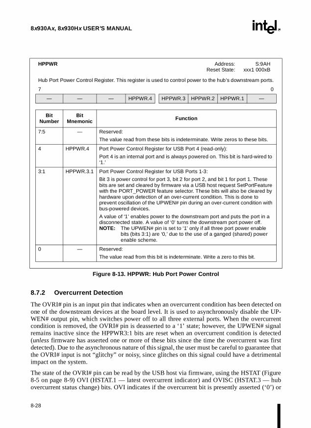
8x930Ax, 8x930Hx USER’S MANUAL
ted onP-rrentignaltecteds first thatntal
igurehub
8.7.2 Overcurrent Detection
The OVRI# pin is an input pin that indicates when an overcurrent condition has been detecone of the downstream devices at the board level. It is used to asynchronously disable the UWEN# output pin, which switches power off to all three external ports. When the overcucondition is removed, the OVRI# pin is deasserted to a ‘1’ state; however, the UPWEN# sremains inactive since the HPPWR3:1 bits are reset when an overcurrent condition is de(unless firmware has asserted one or more of these bits since the time the overcurrent wadetected). Due to the asynchronous nature of this signal, the user must be careful to guaranteethe OVRI# input is not “glitchy” or noisy, since glitches on this signal could have a detrimeimpact on the system.
The state of the OVRI# pin can be read by the USB host via firmware, using the HSTAT (F8-5 on page 8-9) OVI (HSTAT.1 — latest overcurrent indicator) and OVISC (HSTAT.3 — overcurrent status change) bits. OVI indicates if the overcurrent bit is presently asserted (‘0’) or
HPPWR Address: S:9AHReset State: xxx1 000xB
Hub Port Power Control Register. This register is used to control power to the hub’s downstream ports.
7 0
— — — HPPWR.4 HPPWR.3 HPPWR.2 HPPWR.1 —
Bit Number
Bit Mnemonic Function
7:5 — Reserved:
The value read from these bits is indeterminate. Write zeros to these bits.
4 HPPWR.4 Port Power Control Register for USB Port 4 (read-only):
Port 4 is an internal port and is always powered on. This bit is hard-wired to ‘1.’
3:1 HPPWR.3.1 Port Power Control Register for USB Ports 1-3:
Bit 3 is power control for port 3, bit 2 for port 2, and bit 1 for port 1. These bits are set and cleared by firmware via a USB host request SetPortFeature with the PORT_POWER feature selector. These bits will also be cleared by hardware upon detection of an over-current condition. This is done to prevent oscillation of the UPWEN# pin during an over-current condition with bus-powered devices.
A value of ‘1’ enables power to the downstream port and puts the port in a disconnected state. A value of ‘0’ turns the downstream port power off. NOTE: The UPWEN# pin is set to ‘1’ only if all three port power enable
bits (bits 3:1) are ‘0,’ due to the use of a ganged (shared) power enable scheme.
0 — Reserved:
The value read from this bit is indeterminate. Write a zero to this bit.
Figure 8-13. HPPWR: Hub Port Power Control
8-28

USB HUB
bit wasre).
in the self-er to
pin is
ol of
long
deas-
gnals
via thent con-
e dis-
de-asserted (‘1’). OVISC indicates whether the overcurrent status has changed since this first cleared by firmware (i.e., this bit acts as a “sticky” bit which must be cleared in firmwa
Another fact to consider about the overcurrent condition is that all external ports are placed“powered off” state. This is true for both bus-powered and self-powered ports, even thoughpowered ports may still be powered. This condition will remain until the host enables powthe ports via one of the HPPWR.3:1 bits.
8.7.3 Ganged Power Enable
The 8x930Hx uses a ganged power enable scheme to enable power to the three externaldown-stream ports. This means that a single output pin, UPWEN# (pin 60) should be used at theboard-level to switch power to all three of the downstream ports. The state of this power enablecontrolled in two ways:
• by the collective ORed value of bits 3:1 of the HPPWR SFR (Figure 8-13) under contrfirmware, and
• by the present state of the overcurrent sense input pin, OVRI# (pin 59).
If any of the HPPWR[3:1] bits are set, then the UPWEN# signal will be asserted (to a ‘0’) asas the OVRI# signal is not asserted (i.e., OVRI # = ‘1’). If the OVRI# signal is asserted (‘0’), orif all three of the power enable bits in HPPWR are cleared, then the UPWEN# signal will beserted (to a ‘1’).
Table 8-7 describes the state of the UPWEN# signal for all conditions of the HPPWR[3:1] siand the OVRI# pin. Port power enable bits in the HPPWR SFR (Figure 8-13 on page 8-28) areset via the SetPortFeature PORT_POWER request from the USB host. They are clearedClearPortFeature PORT_POWER request, or by hardware upon detection of an overcurredition.
Since a single power enable output is used for three ports, the value of the corresponding HPPWRbit does not necessarily reflect the actual state of the port power, since all three bits must babled for power to be disabled. Similarly, a ‘1’ bit in the HPPWR SFR might not reflect that pow-er is actually enabled to any devices in the event of an overcurrent condition.
Table 8-7. UPWIN# Pin State Truth Table
HPPWR.3 HPPWR.2 HPPWR.1 OVRI# UPWEN#
0 (disabled) 0 (disabled) 0 (disabled) 1 (disabled) 1 (disabled)
X X 1 1 0 (enabled)
X 1 X 1 0
1 X X 1 0
X X X 0 (enabled) 1
8-29

8x930Ax, 8x930Hx USER’S MANUAL
ct the
es is
dix B.
Note that the power enable signal for the internal port, HPPWR (for port 4), does not affestate of the UPWEN# pin. Also, note that bus-powered devices must use the UPWEN# signal toswitch power to downstream ports, however, port power switching for self-powered devicoptional.
NOTEBefore the UPWEN# pin can be enabled, the EP1EN bit in the HSTAT SFR (Figure 8-5 on page 8-9) must be set. See Section 11.9 of the Universal Serial Bus Specification.
8.8 HUB DEVICE SIGNALS
Table 8-8 lists device signals associated with the hub. Pin assignments are shown in Appen
Table 8-8. Signal Descriptions
Signal Name Type Description Alternate
Function
DP0, DM0 I/O USB (Upstream) Port 0 . DP0 and DM0 are the data plus and data minus lines of differential USB port 0. These lines do not have internal pullup resistors. For low-speed devices, provide an external 1.5 KΩ pullup resistor at DM0. For full-speed devices, provide an external 1.5 KΩ pullup resistor at DP0.
NOTE: For the 8x930Hx, provide an external 1.5 KΩ pullup resistor at DP0 so the device indicates to the host that it is a full-speed device.
—
DP1, DM1 I/O USB (Downstream) Port 1 . DP1 and DM1 are the voltage plus and voltage minus lines of differential USB port 1. You must supply an external 15 KΩ pulldown resistor for these lines.
—
DP2, DM2 I/O USB (Downstream) Port 2 . DP2 and DM2 are the voltage plus and voltage minus lines of differential USB port 2. You must supply an external 15 KΩ pulldown resistor for these lines.
—
DP3, DM3 I/O USB (Downstream) Port 3 . DP3 and DM3 are the voltage plus and voltage minus lines of differential USB port 3. You must supply an external 15 KΩ pulldown resistor for these lines.
—
8-30

9USB Programming Models


inter-en theSB re-
erationsterfacetion.”
ils on
CHAPTER 9USB PROGRAMMING MODELS
This chapter describes the programming models of the USB function interface and the hubface. It provides flow charts of firmware routines needed to perform data transfers betwehost PC and the embedded function, as well as routines needed to handle hub-oriented Uquests. It also describes briefly how the firmware interacts with the USB module hardware duringthese operations. Data operations refer to data transfers over the USB, whereas event opare hardware operations such as attach and detach. For a description of the USB function inas well as its FIFOs and special functions registers (SFRs), refer to Chapter 7, “USB FuncFor further information about the USB hub interface, see Chapter 8, “USB Hub.” For detadata flow in USB transactions refer to Appendix D.
Section 9.1 through section 9.5 discuss programming models for the 8x930Ax. These models alsoapply to the embedded function of the 8x930Hx. Section 9.6 contains the hub programming mod-els for the 8x930Hx.
Figure 9-1. Program Flow
Receive SOFTransmit
Unenumerated
Reset
IN token OUT
tokenSETUP token
SOF token
Setup
A4260-02
Idle/Application Code
Receive
9-1

8x930Ax, 8x930Hx USER’S MANUAL
ceiveachr enu-s.
erationque ad-
e for see
ction
o er
,
he
ith the
9.1 OVERVIEW OF PROGRAMMING MODELS
The USB function interface employs four types of routines: receive, transmit, setup, and reSOF. Program flow is depicted in Figure 9-1 along with the type of token associated with eroutine. Following device reset, the USB function enters the unenumerated state and aftemeration by the host, the idle state. From the idle state, it can enter any of the four routine
9.1.1 Unenumerated State
Following device reset, the USB function enters the unenumerated state. Initially, the functionaddress register FADDR contains the default value 00H. The host PC performs bus enumin which it identifies and addresses devices attached to the bus. During enumeration, a unidress assigned by the host is written to FADDR.
NOTEAlthough the 8x930Hx performs the following enumeration process for its embedded function, this process is only part of a larger enumeration process for the hub. 8x930Hx firmware must perform the hub enumeration process outlined in “Bus Enumeration” on page 9-16 before performing the following process.
The 8x930Ax bus enumeration process has four steps:
1. Get descriptor. The host requests and reads the device descriptor to determine such information as device class, USB specification compliance level, maximum packet sizendpoint 0, vendor id, product id, etc. For detailed information on device descriptors,the “Device Framework” chapter in Universal Serial Bus Specification.
2. Set address. The host sends the 8x930’s function address in a data packet using functionendpoint 0. Device firmware interprets the data and instructs the CPU to write the funaddress to FADDR.
3. Get configuration. The host requests and reads the device configuration descriptor tdetermine such information as the number of interfaces and endpoints; endpoint transftype, packet size, and direction; power source; maximum power; etc. For detailed information on configuration descriptors, see the “Device Framework” chapter in Universal Serial Bus Specification. When the host requests the configuration descriptorall related interface and endpoint descriptors are returned.
4. Set configuration. The host assigns a configuration value to the device to establish tcurrent configuration. Devices can have multiple configurations.
9.1.2 Idle State
Following bus enumeration, the USB function enters the idle state. In this state, the 8x930 exe-cutes application code associated with the embedded function. Upon receipt of a token wassigned address, the module enters the designated routine. The 8x930 remains in the idle statewhen not processing USB transmissions.
9-2

USB PROGRAMMING MODELS
ration adjust-th thefer thatd point-ed by
ts, see
ansmitside ofer the-6 and
datapt oft overnanage-
is thenU. Theement
9.1.3 Transmit and Receive Routines
When the 8x930 is sending and receiving packets in the transmit and receive modes, its opedepends on the type of data that is transferred—isochronous or non-isochronous—and thement of the FIFO markers and pointers—automatic or manual. These differences affect bo8x930 firmware and the operation of the 8x930 hardware. For isochronous data, a failed transis not retried (lossy data). For non-isochronous data, a failed transfer can be repeated. Datacan be repeated is considered lossless data. Automatic adjustment of the FIFO markers aners is accomplished by the function interface hardware. Manual adjustment is accomplishthe 8x930 firmware.
9.1.4 USB Interrupts
For an explanation of the USB global suspend/resume, function, hub, and SOF interrupChapter 6, “Interrupt System.”
9.2 TRANSMIT OPERATIONS
9.2.1 Overview
A transmit operation occurs in three major steps:
1. Pre-transmit data preparation by firmware
2. Data packet transmission by function interface hardware
3. Post-transmit management by firmware
These steps are depicted in a high-level view of transmit operations (Figure 9-2). The pre-trand post-transmit operations are executed by the two firmware routines shown on the left the figure. Function interface hardware (right side of the figure) transmits the data packet ovUSB line. Details of these operations are described in “Pre-transmit Operations” on page 9“Post-transmit Operations” on page 9-7.
Transmit operations for non-isochronous data begin with an interrupt request from the embeddedfunction (e.g., a keyboard entry). The pre-transmit routine (ISR) for the function writes thefrom the function to the transmit FIFO where it is held until the next IN token. Upon receithe next valid IN token, the function interface shifts the data out of the FIFO and transmits ithe USB. If the data packet is not ready for transmission, 8x930 hardware responds to the IN tokewith a NAK. The post-transmit routine checks the transmission status and performs data mment tasks.
Completion of data transmission is indicated by a handshake returned by the host. This used to generate a transmit done interrupt to signal the end of data transmission to the CPinterrupt can also be used for activity tracking and fail-safe management. Fail-safe managpermits recovery from lockups that can only be cleared by firmware.
9-3

8x930Ax, 8x930Hx USER’S MANUAL
o
s
initi-, andupdated
ajor
ta
nsmit
re
Because a transmit done interrupt is generated regardless of transmission errors, this conditionmeans either:
1. The transmit data has been transmitted and the host has sent an acknowledgment tindicate that is was successfully received; or
2. A transmit data error occurred during transmission of the data packet, which requireservicing by firmware to be cleared. You must check for these conditions and respond accordingly in the ISR.
For ISO data transmission, the cycle is similar. The significant differences are: the cycle isated by a start-of-frame (SOF) interrupt, there is no handshake associated with ISO transfera transmit done interrupt is not generated. For ISO data transfers, the transaction status is at the end of the USB frame. The 8x930 supports one ISO packet per frame per endpoint.
Two bits in the transmit FIFO control register (TXCON, Figure 7-12 on page 7-24) have a minfluence on transmit operation:
• The TXISO bit (TXCON.3) determines whether the transmission is for isochronous da(TXISO = 1) or non-isochronous data (TXISO = 0). For non-isochronous data only, the function interface receives a handshake from the host, toggles or does not toggle the sequence bit, and generates a transmission done interrupt (Figure 9-2). Also, for non-isochronous data, the post-transmit routine is an ISR; for isochronous data the post-traroutine is an ISR initiated by an SOF token.
• The ATM bit (TXCON.2) determines whether the FIFO read marker and read pointer amanaged automatically by the FIFO hardware (ATM = 1) or manually by the second firmware routine (ATM = 0). Use of the ATM mode is recommended. The ADVRM andREVRP bits, which control the read marker and read pointer when ATM = 0, are usedprimarily for test purposes. See bit definitions in TXCON (Figure 7-12).
9-4

USB PROGRAMMING MODELS
Figure 9-2. High-level View of Transmit Operations
Interrupt (keyboard, joystick, modem)
ISR
Write data to transmit FIFO Write TXCNT
TXISO = 0: Transmit done interrupt TXISO = 1: SOF interrupt
IN Token
Send data over USB
RETI
Firmware Hardware
RETI
– Receive host handshake – Manage TXSEQ bit
If TXISO = 0:
If ATM = 1:
A4262-02
(SIE, FIU, FIFOs)
Post- Transmit Routine
Pre-transmit Routine
– Adjust FIFO read marker and read pointer
– Adjust FIFO read marker and read pointer
• •
••
ISR
Check status If ATM = 0:
• •
•
Generate transmit done interrupt or SOF interrupt
•
9-5

8x930Ax, 8x930Hx USER’S MANUAL
e, joy-f data pre-re 9-3
se to a
9.2.2 Pre-transmit Operations
Transmitted data originates in the embedded function, which might be a keyboard, mousstick, scanner, etc. In event-control applications, the end function signals the availability owith an interrupt request for the pre-transmit interrupt service routine (ISR). The ISR shouldpare the data for transmission and initiate the transmission process. The flow chart in Figuillustrates a typical pre-transmit ISR.
For the case of isochronous data, the interrupt is triggered by the USB function in responstart-of-frame (SOF) packet.
Figure 9-3. Pre-transmit ISR (Non-Isochronous)
RETI
Start: Non-ISO
A5071-01
Yes
No
Yes
NoVacancy in Transmit
FIFO?
Transfer Packet to Transmit FIFO through
TXDAT
TXFIF1:0 = 11 in Dual-packet Mode TXFIF1:0 = 00 in Single-packet Mode
Write Packet Size to TXCNT
Error in Transmit FIFO? TXOVF = 1 (overflow)
Error Recovery
9-6

USB PROGRAMMING MODELS
received
rupt. ensureuld be
flow of
9.2.3 Post-transmit Operations
Transmission status is updated at the end of data transmission based on the handshake from the host (non-isochronous data) or based on the transmission process itself (isochronousdata). For a non-isochronous transfer, the function interface generates a transmit done interThe purpose of the post-transmit service routines is to manage the transmitter’s state and todata integrity for the next transmission. For isochronous data, the post-transmit routine shoembedded within the transfer request routine because both are triggered by an SOF. Theoperations of typical post-transmit ISRs is illustrated in Figure 9-4 (non-isochronous data) andFigure 9-5 (isochronous data).
Figure 9-4. Post-transmit ISR ( Non-isochronous)
RETI
Identify Interrupt and Endpoint (check FTXDx bits in FIFLG register)
Start: Transmit Done ISR
A5072-01
No(TXACK = 1) Yes
Read Transaction Status (TXSTAT Register)
Clear Interrupt Flag (FTXDx Bit)
Transmit Error?
(TXERR = 1)
Error in Transmit FIFO?
Yes
Data Error recovery
Reverse Transmit FIFO to Current Packet Retry
No
Failed CRC, Bit-stuffing, or Timeout from Host
Advance Transmit FIFO to Next Packet Transmit
(Underrun Flag TXURF = 1?)
Buffer Segmentation Management. Executed automatically by hardware, based on transaction status, if ATM bit in TXCON is set.
†
† †
9-7

8x930Ax, 8x930Hx USER’S MANUAL
Figure 9-5. Post-transmit ISR (Isochronous)
No
RETI
Start: SOF ISR
A5073-02
Check TXFLUSH (error tracking)
Overflow Error in Transmit
FIFO?
No
Yes (TXURF = 1)
YesNoFor
Each Endpoint, Read Transaction Status
(TXSTAT) Transmit Error?
Write Next Packet to Transmit FIFO
(TXERR = 1)(TXACK = 1)
Error in Transmit FIFO?
Advance Transmit FIFO to next packet No
(Failed CRC, Bit Stuffing, or Timeout from Host)
Transmit FIFO Error Recovery
Write Packet Size to TXCNT
Error Recovery
Buffer Segmentation Management. Executed automatically by hardware at the end of a data transaction if ATM bit in TXCON is set. For isochronous transactions, there is no retry of current packet regardless of transaction status.
†
Write Packet Size to TXCNT
Write Next Packet to Transmit FIFO
Advance Transmit FIFO to Next Packet
Overflow Error in Transmit
FIFO?(TXOVF = 1)
Yes
(TXOVF = 1)Yes
†
†
9-8

USB PROGRAMMING MODELS
post-e. For of fig-
PUinelso be
d by an
for post
ajor
= 1) ce
ne for
are P ly
9.3 RECEIVE OPERATIONS
9.3.1 Overview
A receive operation is always initiated by the host, which sends an OUT token to the 8x930. Theoperation occurs in two major steps:
1. Data packet reception by the function interface (hardware)
2. Post-receive management by firmware
These steps are depicted in a high-level view of the receive operations in Figure 9-6. Thereceive operations are executed by the firmware routine shown on the left side of the figurdetails see “Post-receive Operations” on page 9-10. Function interface hardware (right sideure) receives the data packet over the USB line.
Receive operations for non-isochronous data begin when the 8x930 receives a valid OUT tokenfrom the host. The received data is written to a data buffer FIFO. The 8x930 indicates completionof data received by returning a handshake to the host.
At the end of the receive cycle, the 8x930 generates a receive done interrupt to notify the Cthat a receive operation has occurred. Program execution branches to the interrupt service routand transfers the data packet from the receive FIFO to its destination. The interrupt can aused for fail-safe management and activity tracking.
For isochronous data, receive cycles are somewhat different. Data transactions are initiateOUT token. At the end of the OUT transaction, the 8x930Ax does not return handshake to thehost and the receive done interrupt is not generated. Instead, the SOF interrupt is used receive management. The data reception status is updated at the next SOF. The 8x930 supportsone ISO packet per frame per endpoint.
Two bits in the receive FIFO control register (RXCON, Figure 7-15 on page 7-29) have a minfluence on receive operation:
• The ISO bit (RXCON.3) determines whether the reception is for isochronous data (ISOor non-isochronous data (ISO = 0). For non-isochronous data only, the function interfasends a handshake to the host, checks the sequence bit, and generates a receive-do(FRXDx) interrupt. Also, for non-isochronous data, the post-receive routine is an ISR; isochronous data the post-receive routine can be a normal subroutine or ISR initiated by an SOF token.
• The ARM bit (RXCON.2) determines whether the FIFO write marker and write pointer managed automatically by the FIFO hardware (ARM = 1) or manually by the firmwareroutine (ARM = 0). Use of the ARM mode is recommended. The ADVWM and REVWbits, which control the write marker and write pointer when ARM = 0, are used primarifor test purposes. See bit definitions in RXCON (Figure 7-15).
9-9
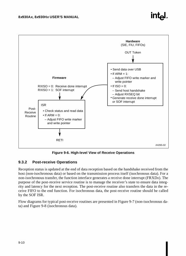
8x930Ax, 8x930Hx USER’S MANUAL
from the
a integ-the re- called
us da-
Figure 9-6. High-level View of Receive Operations
9.3.2 Post-receive Operations
Reception status is updated at the end of data reception based on the handshake receivedhost (non-isochronous data) or based on the transmission process itself (isochronous data). For anon-isochronous transfer, the function interface generates a receive done interrupt (FRXDx). Thepurpose of the post-receive service routine is to manage the receiver’s state to ensure datrity and latency for the next reception. The post-receive routine also transfers the data in ceive FIFO to the end function. For isochronous data, the post-receive routine should beby the SOF ISR.
Flow diagrams for typical post-receive routines are presented in Figure 9-7 (non-isochronota) and Figure 9-8 (isochronous data).
RXISO = 0: Receive done interrupt RXISO = 1: SOF interrupt
ISR
OUT Token
Firmware
Hardware
RETI
A4265-02
(SIE, FIU, FIFOs)
Post- Receive Routine
Send data over USB
– Send host handshake – Adjust RXSEQ bit Generate receive done interrupt or SOF interrupt
If ISO = 0:
If ARM = 1:– Adjust FIFO write marker and write pointer
••
•
Check status and read data If ARM = 0:– Adjust FIFO write marker and write pointer
••
•
9-10

USB PROGRAMMING MODELS
Figure 9-7. Post-receive ISR (Non-isochronous)
No
RETI
Start: Receive Done ISR
Clear Interrupt Flag
Identify Function Interrupt and Endpoint (Check FRXDx Bits in FIFLG Register)
Error in Receive FIFO?
No
Yes (RXOVF=1)
Yes
YesNoCheck
RXSTAT for Receive
Error
Read Data Packet(s)
(RXERR=1)(RXACK=1)
Error in Receive FIFO?
Advance Receive FIFO to next packet
Reverse Receive FIFO to current packet retry
No(Failed CRC or Bit Stuffing)
Receive FIFO Error Recovery
Check for Another Packet in
Receive FIFO (RXFIF1:0 = 00 in Dual
Port Mode)
Receive FIFO Error Recovery
Unlock Current Packet from Receive FIFO (set RXFFRC
Bit in RXCON)
Buffer Segmentation Management. Executed automatically by hardware at the end of a data transaction if ARM bit in RXCON is set.
†
†
†
A5070-01
Yes (RXURF = 1)
(RXOVF=1)
9-11

8x930Ax, 8x930Hx USER’S MANUAL
Figure 9-8. Receive SOF ISR (Isochronous)
Yes
RETI
Start: SOF ISR
A5074-01
Error in Receive
FIFO?
Yes (RXOVF = 1)
YesNoFor
Each Endpoint, Read Transaction Status
(RXSTAT) Transmit Error?
Read Data Packet
(RXERR = 1)(RXACK = 1)
Error in Receive FIFO?
Advance Receive FIFO to Next Packet No
(Failed CRC or Bit Stuffing)
Receive FIFO Error Recovery
Data Reconstruction by Application for
Lost Data
Receive FIFO Error Recovery
Unlock Current Packet from Receive FIFO
(set RXFFRC bit in RXCON)
Buffer Segmentation Management. Executed automatically by hardware at the end of a data transaction if ARM bit in TXCON is set. For isochronous transactions, there is no retry of current packet regardless of transaction status.
†
(RXURF = 1)
No
Advance Receive FIFO to Next Packet Receive
Data Reconstruction by Application for
Lost Data
†
†
Unlock FIFO (set RXFFRC)
9-12

USB PROGRAMMING MODELS
ayer”
ood).n non-ferent
a set-- naturet this,ite is, users the
9.4 SETUP TOKEN
An endpoint must be configured as a control endpoint in order to respond to SETUP tokens. (Thiswill only be endpoint 0, since it must serve as a control endpoint.) Refer to the “Protocol Lsection of the Universal Serial Bus Specification for details of SETUP token transactions and pro-tocol.
A control data transfer is initiated by a valid SETUP token (i.e., the token PID received is gReceive data transfer operations for a control endpoint are very similar to data transfers ocontrol endpoints for non-setup tokens. However, the response of a control endpoint is difwhen it receives a setup token.
USB protocol specifies that setup tokens must be received and ACKed. Following receipt ofup token, a control endpoint flushes the contents of the receive FIFO before writing it with received setup data. This may create an error condition in the FIFO due to the asynchronousof FIFO reads by the CPU and simultaneous writes by the function interface. To prevenSTOVW and EDOVW are used to track when an overwrite is occurring. When the overwrcomplete, the user must clear EDOVW to read the SETUP packet. If EDOVW is not clearedfirmware will only be able to read the first byte of the SETUP packet. Figure 9-9 illustrateoperations of a typical post-receive routine for a control endpoint.
9-13

8x930Ax, 8x930Hx USER’S MANUAL
Figure 9-9. Post-receive ISR (Control)
RETI
Start: Receive Done ISR
A5075-01
No
YesNo
Read Data Packet
OUT Token Received
Clear Firmware Setup Flag
Setup Token Received Clear EDOVW
(RXERR = 1)(RXACK = 1)
Clear Overwrite Bit (EDOVW)
Unlock Current Packet from Receive FIFO
(set RXFFRC bit in RXCON)
Inhibited in hardware if STOVW or EDOVW are asserted.†
No
No
Yes (STOVW = 0 and EDOVW = 1)
Yes (STOVW = 1 or EDOVW = 1)
Normal Error
Handling
†
Identify Interrupt Endpoint (check FRXDx bits in the FIFLG register) Clear Interrupt Flag
Check RXSTAT for
Receive Error
Setup Token?
Yes (RXSETUP = 1)
Overwrite Completed?
Receive FIFO Overwrite?
Error in Receive FIFO?
No
No
Yes
Error Recovery
(RXURF = 1)
Yes
Yes
Clear Overwrite Bit (EDOVW)
No
Overwrite Completed
Receive FIFO Overwrite?
(STOVW = 0 and EDOVW = 0)
(STOVW = 1 or EDOVW = 1)
(STOVW = 0 and EDOVW = 1)
(STOVW = 0 and EDOVW = 0)
9-14

USB PROGRAMMING MODELS
art-of-n SOF
ed by
9.5 START-OF-FRAME (SOF) TOKEN
Figure 9-10 illustrates the hardware operations performed by the function interface for a stframe (SOF) token. The host issues an SOF token at a nominal rate of once every 1.0 ms. Atoken is valid if the PID is good. The SOF token is not endpoint-specific; it should be receivevery node on the bus.
Figure 9-10. Hardware Operations for SOF Token
Set ASOF Bit
End of Transfer
No
Pass CRC?
Yes
Write SOF Registers
Clear SOFACK
Bit
Done
Yes
Valid SOF Token
No
Set SOFACK. (SOF token received
without error)
Generate SOF Pulse by Asserting SOF# Pin
(SOFH.7)
(SOFH.7)
(SOFH, SOFL)
(SOFH.6)
A4267-02
9-15

8x930Ax, 8x930Hx USER’S MANUAL
be-
ce is at-edrformsnumer-
e such e for
int s to
nd
he
. The red in
re to n e.
he host the ature ster.
9.6 HUB OPERATION
The primary objective of the programming model suggested here is to explain the linkage tween the hardware and firmware of the 8x930Hx in operation.
9.6.1 Bus Enumeration
The USB host manages bus enumeration at system start-up or whenever a new USB devitached to the host or to a hub’s downstream port. Initially, the USB hub is in the unenumeratstate and the hub address register HADDR contains the default value 00H. The host PC pebus enumeration in which it identifies and addresses devices attached to the bus. During eation, a unique address assigned by the host is written to the HADDR of the hub device. An ex-ample enumeration for the hub and downstream ports is given here:
1. Get device descriptor. The host requests and reads the device descriptor to determininformation as device class, USB specification compliance level, maximum packet sizendpoint 0, vendor id, product id, etc. For additional information on the 8x930Hx descriptors, see “Hub Descriptors” on page 8-6.
2. Set address. The host sends the 8x930Hx’s hub address in a data packet using hub endpo0. Device firmware interprets the data and instructs the CPU to write the hub addresHADDR. See “The Hub Address Register (HADDR)” on page 8-8.
3. Get configuration descriptor. The host requests and reads the device’s configurationdescriptor to determine such information as the number of interfaces and endpoints;endpoint transfer type, packet size, and direction; power source; maximum power; etc. When the host requests the configuration descriptor, all related interface, endpoint, ahub descriptors are returned. For additional information on the 8x930Hx descriptors, see “Hub Descriptors” on page 8-6.
4. Set configuration. The host assigns a configuration value to the device to establish tcurrent configuration.
5. Next, the hub downstream ports start the state flow shown in Figure 8-2 on page 8-4host issues a SetPortPowerFeature request to the downstream ports that were declathe hub descriptor. This moves the hub downstream ports to the disconnect state.
6. As connect detects occur, the host is notified through hub endpoint 1 (status changeendpoint). The host then issues a GetPortStatus command retrieving the contents ofHPSTAT and HPSC to determine the change for a specific downstream port. The host then issues a ClearPortConnectionFeature command which should cause the firmwaclear the PCSC bit in the HPSC register. This will indirectly clear the appropriate bit iTXDAT for hub endpoint 1. This moves the hub downstream port to the disabled stat
7. The host sends a SetPortResetFeature request for the specified downstream port. Treceives a response through hub endpoint 1 (status change endpoint). The host issues aGetPortStatus command retrieving the contents of HPSTAT and HPSC to determinechange for the specified downstream port. The host then issues a ClearPortResetFecommand which should cause the firmware to clear the RSTSC bit in the HPSC regiThis moves the hub downstream port to the enabled state.
9-16

USB PROGRAMMING MODELS
s-spe-ub andstream phys-SB re-
b end-
8. At this point, the device connected to the downstream port goes through the enumeration process discussed in “Unenumerated State” on page 9-2 (i.e., GetDeviceDescriptor,SetAddress, GetConfigurationDescriptor, and SetConfiguration).
9. The remaining external ports must go through steps 6 through 8.
9.6.2 Hub Status and Configuration
USB communication with the USB hub function is performed via the standard and hub clascific USB requests. These requests control status management and configuration of the hits downstream ports. Since the hub is part of a compound device, it has an internal downport (port 4) which is unique from the external downstream ports. This is because port 4 isically connected to the embedded function and is powered-on at all times. Thus several Uquests intended for internal downstream port 4 are handled differently from similar requests tothe other downstream ports, as shown in Table 8-6 on page 8-16.
Table 9-1 is a summary of firmware actions required for standard USB requests sent to hupoint 0.
Table 9-1. Firmware Actions for USB Requests Sent to Hub
USB Request Feature Selector / Type Firmware Action Required
SET_FEATURE
DEVICE_REMOTE_WAKEUP
Set the HRWUPE bit of the HSTAT SFR. See “Hub Status” on page 8-8.
ENDPOINT_STALL
Stall the endpoint specified in the Setup PID. See “Hub Endpoint Control” on page 8-11.
Endpoint 0 specified: 1. Load 80H into EPINDEX (for hub endpoint 0)2. Set RXSTL and TXSTL bits of EPCON SFR.
Endpoint 1 specified:
Set EP1STL bit of HSTAT SFR.
CLEAR_FEATURE
DEVICE_REMOTE_WAKEUP
Clear HRWUPE bit of HSTAT SFR. See “Hub Status” on page 8-8.
ENDPOINT_STALL
Cancel stall for the specified endpoint. See “Hub Endpoint Control” on page 8-11.
Endpoint 0 specified: 1. Load 80H into EPINDEX (for hub endpoint 0)2. Clear RXSTL and TXSTL bits of EPCON SFR
Endpoint 1 specified:
Clear EP1STL bit of HSTAT SFR.
SET_CONFIGURATION N/A
1. Store hub endpoint 1 configuration value from value field in memory
2. Set EP1EN bit of HSTAT SFR (Figure 8-5 on page 8-9) after the Status stage if 2-byte configuration value = 0001H
GET_CONFIGURATION N/A Read configuration value (one byte) from memory and send to the host.
9-17

8x930Ax, 8x930Hx USER’S MANUAL
Table 9-2 summarizes firmware action for hub class-specific USB requests.
NOTEUpon receipt of a state-related USB request (i.e., SetPortFeature, ClearPortFeature), firmware must examine the HPSTAT SFR to determine the current port state. If the port is in a state where the request will be ignored by
GET_DESCRIPTOR
Device Read device descriptor from memory and transmit to USB host through hub endpoint 0.
ConfigurationRead configuration, interface, endpoint, and hub descriptors from memory and transmit to USB host through hub endpoint 0.
GET_INTERFACE N/A
Optional request for hubs which is not supported. 1. Load 80H into EPINDEX (for hub endpoint 0)2. Set TXSTL bit of EPCON SFR so STALL is sent
during status stage
GET_STATUS
DeviceRead HSTAT SFR bit HRWUPE (Figure 8-5 on page 8-9) and power configuration from memory and transmit to USB host using hub endpoint 0.
InterfaceLoad 2 bytes of zero into transmit buffer and transmit to USB host. These bits are reserved in the initial version of USB.
Endpoint
Endpoint 0 specified:
Load transmit buffer with value of zero if endpoint 0 is not stalled. No data can be returned if endpoint 0 is stalled, since STALL will be transmitted instead.
Endpoint 1 specified:
Load value of EP1STL bit of HSTAT SFR into transmit buffer (Figure 8-5 on page 8-9).
SET_ADDRESS N/A
Read address value contained in request value field and store in HADDR SFR (Figure 8-4 on page 8-8) after successful completion of control transaction status stage.
SET_DESCRIPTOR N/A
Optional request for hubs which is not supported. 1. Load 80H into EPINDEX (for hub endpoint 0)2. Set TXSTL bit of EPCON SFR so STALL is sent
during status stage
SET_INTERFACE N/A
Optional request for hubs which is not supported. 1. Load 80H into EPINDEX (for hub endpoint 0)2. Set TXSTL bit of EPCON SFR so STALL is sent
during status stage
SYNCH_FRAME N/A
Optional request for hubs which is not supported. 1. Load 80H into EPINDEX (for hub endpoint 0)2. Set TXSTL bit of EPCON SFR so STALL is sent
during status stage
Table 9-1. Firmware Actions for USB Requests Sent to Hub (Continued)
USB Request Feature Selector / Type Firmware Action Required
9-18
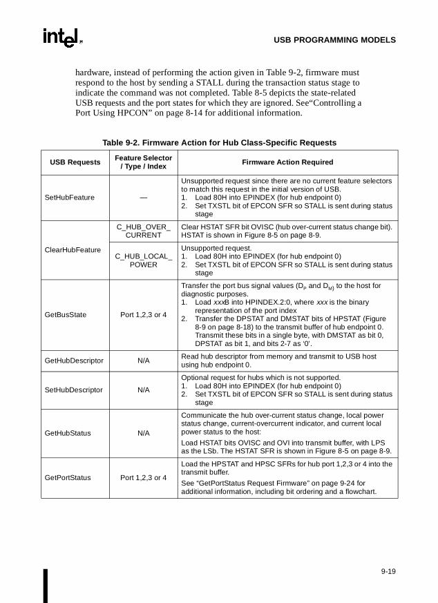
USB PROGRAMMING MODELS
hardware, instead of performing the action given in Table 9-2, firmware must respond to the host by sending a STALL during the transaction status stage to indicate the command was not completed. Table 8-5 depicts the state-related USB requests and the port states for which they are ignored. See“Controlling a Port Using HPCON” on page 8-14 for additional information.
Table 9-2. Firmware Action for Hub Class-Specific Requests
USB Requests Feature Selector / Type / Index Firmware Action Required
SetHubFeature —
Unsupported request since there are no current feature selectors to match this request in the initial version of USB. 1. Load 80H into EPINDEX (for hub endpoint 0)2. Set TXSTL bit of EPCON SFR so STALL is sent during status
stage
ClearHubFeature
C_HUB_OVER_CURRENT
Clear HSTAT SFR bit OVISC (hub over-current status change bit). HSTAT is shown in Figure 8-5 on page 8-9.
C_HUB_LOCAL_POWER
Unsupported request. 1. Load 80H into EPINDEX (for hub endpoint 0)2. Set TXSTL bit of EPCON SFR so STALL is sent during status
stage
GetBusState Port 1,2,3 or 4
Transfer the port bus signal values (DP and DM) to the host for diagnostic purposes.1. Load xxxB into HPINDEX.2:0, where xxx is the binary
representation of the port index2. Transfer the DPSTAT and DMSTAT bits of HPSTAT (Figure
8-9 on page 8-18) to the transmit buffer of hub endpoint 0. Transmit these bits in a single byte, with DMSTAT as bit 0, DPSTAT as bit 1, and bits 2-7 as ‘0’.
GetHubDescriptor N/A Read hub descriptor from memory and transmit to USB host using hub endpoint 0.
SetHubDescriptor N/A
Optional request for hubs which is not supported. 1. Load 80H into EPINDEX (for hub endpoint 0)2. Set TXSTL bit of EPCON SFR so STALL is sent during status
stage
GetHubStatus N/A
Communicate the hub over-current status change, local power status change, current-overcurrent indicator, and current local power status to the host:
Load HSTAT bits OVISC and OVI into transmit buffer, with LPS as the LSb. The HSTAT SFR is shown in Figure 8-5 on page 8-9.
GetPortStatus Port 1,2,3 or 4
Load the HPSTAT and HPSC SFRs for hub port 1,2,3 or 4 into the transmit buffer.
See “GetPortStatus Request Firmware” on page 9-24 for additional information, including bit ordering and a flowchart.
9-19

8x930Ax, 8x930Hx USER’S MANUAL
SetPortFeature
PORT_ENABLE
Enables address and endpoint decoding for the downstream ports. For hub port 4, this enables address and endpoint decoding for the embedded function.1. Load xxxB into HPINDEX.2:0, where xxx is the binary
representation of the port index2. Write “001” to bits 2:0 of the port’s HPCON SFR (Figure 8-8
on page 8-15)
PORT_SUSPEND
Write “011” to bits 2:0 of the port’s HPCON SFR.
If hub port 4 is specified, the user cannot suspend the embedded function without also suspending the hub. Firmware must suspend any non-hub functionality associated with the embedded function prior to writing to HPCON. This is done by placing any external device hardware into a low-power suspend mode.
See “SetPortFeature (PORT_SUSPEND) Firmware” on page 9-26 for additional information and a flowchart.
PORT_RESET
Write “010” to bits 2:0 of the port’s HPCON SFR.
If port 4 is specified, firmware needs to reset all non-hub functionality in the microcontroller. Upon writing to port 4’s HPCON SFR, a hardware reset is generated to the FIU and function FIFOs. Firmware must gracefully shut-down the application code, peripherals, etc. prior to writing to port 4’s HPCON. Once written, the reset will be active in hardware for 10-11 ms.
See “SetPortFeature (PORT_RESET) Firmware” on page 9-27 for additional information and a flowchart.
PORT_POWER
Set bit x of HPPWR (where x is the port specified in the request index field)
Port power-on is also supported for port 4, but only for reasons of port compatibility since power for the embedded function cannot be switched (i.e., writing bit 4 of HPPWR does not affect any hardware).
Table 9-2. Firmware Action for Hub Class-Specific Requests (Continued)
USB Requests Feature Selector / Type / Index Firmware Action Required
9-20

USB PROGRAMMING MODELS
ClearPortFeature
PORT_ENABLE
Requests port disable. 1. Load xxxB into HPINDEX.2:0, where xxx is the binary
representation of the port index2. Write “000” to bits 2:0 of the port’s HPCON SFR (Figure 8-8
on page 8-15)
For hub port 4, this will disable address and endpoint decoding for the embedded function.
PORT_SUSPEND
Requests port resume. 1. Load xxxB into HPINDEX.2:0, where xxx is the binary
representation of the port index2. Write “100” to bits 2:0 of the port’s HPCON SFR (Figure 8-8
on page 8-15)
If port 4 is specified, firmware must also resume any non-hub functionality associated with the embedded function prior to writing to port 4’s HPCON. This requires taking any external device hardware out of a low-power suspend mode.
PORT_POWER
Request port power off.
If any port other than port 4 is specified:
Clear bit x of HPPWR (where x is the port specified in the request index field)
Port power off is not supported for port 4. If port 4 is specified:1. Load 80H into EPINDEX (for hub endpoint 0)2. Set TXSTL bit of EPCON SFR so STALL is sent during status
stage
C_PORT_CONNECTION
Request to clear port connect status change.1. Load xxxB into HPINDEX.2:0, where xxx is the binary
representation of the port index2. Clear PCSC bit of HPSC SFR (Figure 8-10 on page 8-21)
C_PORT_ENABLE
Request to clear hardware-initiated port enable/disable status change. 1. Load xxxB into HPINDEX.2:0, where xxx is the binary
representation of the port index2. Clear PESC bit of HPSC SFR (Figure 8-10 on page 8-21)
C_PORT_SUSPEND
Request to clear port suspend status change. 1. Load xxxB into HPINDEX.2:0, where xxx is the binary
representation of the port index2. Clear PSSC bit of HPSC SFR (Figure 8-10 on page 8-21)
C_PORT_OVERCURRENT
Unsupported request to clear port over-current status change. The 8x930Hx implements over-current detection on a hub-wide basis, not on a per-port basis. If received:1. Load 80H into EPINDEX (for hub endpoint 0)2. Set TXSTL bit of EPCON SFR so STALL is sent during status
stage
C_PORT_RESET
Request to clear port reset status change. 1. Load xxxB into HPINDEX.2:0, where xxx is the binary
representation of the port index2. Clear RSTSC bit of HPSC SFR (Figure 8-10 on page 8-21)
Table 9-2. Firmware Action for Hub Class-Specific Requests (Continued)
USB Requests Feature Selector / Type / Index Firmware Action Required
9-21

8x930Ax, 8x930Hx USER’S MANUAL
e host.
teps:
the hub rent
nge in
t port’s is
rent
ature will
9.6.3 Port Status Change Communication
The flowchart in Figure 9-11 shows how the hub communicates a change in port status to thThis process involves 8X930Hx hardware, 8X930Hx firmware, and PC host firmware. The flow-chart illustrates the complete process at a high level. The process contains the following s
1. Any change in a port’s reset, suspend, enable, or connect status is communicated tohost via hub endpoint 1’s TXDAT register, as shown in Figure 8-7 on page 8-13. Theinformation passed through hub endpoint 1 is sufficient to indicate which port (or theitself) changed status, but it does not indicate which status value changed or the curvalue of any status indicator.
Firmware has no involvement with USB communication to hub endpoint 1 (status chaendpoint 1). This communication is handled completely in hardware and is discussed“USB Hub Endpoints” on page 8-10
2. After the host receives notice of a change in port status through hub endpoint 1, hosfirmware can determine which status value changed and the current value of all the status indicators by transmitting a GetPortStatus request through hub endpoint 0. Threquest includes a Port_Index to tell the 8X930Hx which port is of interest to the host. Seethe Universal Serial Bus Specification for additional information.
3. The host’s GetPortStatus request triggers the 8x930Hx’ GetPortStatus routine. The firmware response to the GetPortStatus request provides the host with the port’s curstatus along with an indication of any status changes that have occurred. See “GetPortStatus Request Firmware” on page 9-24 for a complete description of this routine.
4. The host resets the port status change indicators by issuing a separate ClearPortFerequest for each bit in HPSC that showed a change. Each ClearPortFeature requestinclude one of the following feature selectors:
a. C_PORT_CONNECTION — to clear HPSC.PCSC
b. C_PORT_ENABLE — to clear HPSC.PESC
c. C_PORT_SUSPEND— to clear HPSC.PSSC
d. C_PORT_RESET — to clear HPSC.RSTSC
5. 8x930Hx firmware responds to each ClearPortFeature request by performing the actions shown in Table 9-2 on page 9-19.
6. Finally, the host must perform any actions necessitated by the status change.
9-22

USB PROGRAMMING MODELS
emain-n ad-
Figure 9-11. Hub-to-host Port Status Communication
9.6.4 Hub Firmware Examples
Several of the firmware routines given in Table 9-2 have been selected as examples. The ring routines should be coded similarly. The following subsections contain a flowchart and aditional explanation for these routines:
• GetPortStatus (Port_Index)
A5207-01
8X930Hx communicates change in port status to host via hub endpoint 1
Status Change Communication
Host inquires into status change via a
GetPortStatus command
Firmware responds through the
GetPortStatus request routine
Host clears bits of HPSC one at a time through
ClearPortFeature commands
Firmware clears HPSC bits through ClearPortFeature
routines
Host performs any actions necessitated by
status change
End
9-23

8x930Ax, 8x930Hx USER’S MANUAL
chart
ctive-e con-
• SetPortFeature (PORT_SUSPEND)
• SetPortFeature (PORT_RESET)
9.6.4.1 GetPortStatus Request Firmware
Firmware responds to a GetPortStatus call by returning four bytes to the host using the flowprocedure shown in Figure 9-12. The four bytes are arranged into a two-byte port status field anda two-byte port change field containing the contents of the HPSTAT and HPSC SFRs, respely. Figure 9-13 shows the relationship between the four bytes returned by firmware and thtents of the HPSTAT and HPSC registers.
Figure 9-12. GetPortStatus Request
Transferring the contents of HPSTAT and HPSC into TXDAT requires additional code not shownin the flowchart. The bits of HPSTAT must be “converted” into a two-byte port status field, as
A5208-01
Write 80H to EPINDEX to access
hub endpoint 0's TX registers
Start: GetPortStatus Request
Write xxxB to HPINDEX (xxx = port number)
to access port's HP registers
Transfer HPSTAT to TXDAT using
two-byte format
Transfer HPSC to TXDAT using two-byte
format
Put 04H in TXCNTL (to indicate 4 bytes ready to transmit)
End
9-24

USB PROGRAMMING MODELS
-
heFirm-ition).
shown in Figure 9-13, and transmitted to the host LSB first. The bits of HPSC must also be transmitted in a two-byte format, called the port change field.
The bit names are given in Figure 9-13, along with their position in the register (shown below tbit name) and their position in the transmitted two-byte field (shown above the bit names). ware must transmit the four bytes to the host in the byte order indicated (above the bit pos
NOTEThe HPSTAT bits are not directly mapped into the port status field. Firmware must clear bit three of byte one to indicate that power is normal (not overcurrent) for the port. This is done because the 8x930Hx indicates overcurrent on a ganged, not per-port, basis.
Figure 9-13. Firmware Response to GetPortStatus
A5117-01
PC
SC
PE
SC
PS
SC
RS
TS
C
Reserved
01234
HPSC
PC
ST
AT
PE
ST
AT
PS
ST
AT
0
Reser
ved
PR
ST
AT
PP
ST
AT
Reserved
LSS
TA
T
012345
HPSTAT
Get Port
Status
0781507815
Port Change FieldPort Status FieldByte 3Byte 4Byte 1Byte 2
0
9-25

8x930Ax, 8x930Hx USER’S MANUAL
ed is in-d any hard-
9.6.4.2 SetPortFeature (PORT_SUSPEND) Firmware
This USB request suspends the downstream ports. The number of the port to be suspendcluded in the request from the host. If hub port 4 is specified, firmware must also suspennon-hub functionality associated with the embedded function and place any external deviceware into low-power suspend mode prior to writing to hub port 4’s HPCON SFR.
To implement this routine, firmware must write “011” to bits 2:0 of the port’s HPCON SFR. Theflowchart in Figure 9-14 illustrates the process.
Figure 9-14. SetPortFeature (PORT_SUSPEND) Routine
A5166-01
Write xxxB to HPINDEX
(xxx = port number) to select the port
End
Write 011B to HPCON to
suspend the port
Is Suspend for port 4?
Place embedded function and its external device
hardware into low- power suspend
mode
Yes
No
SetPortFeature (PortSuspend)
9-26
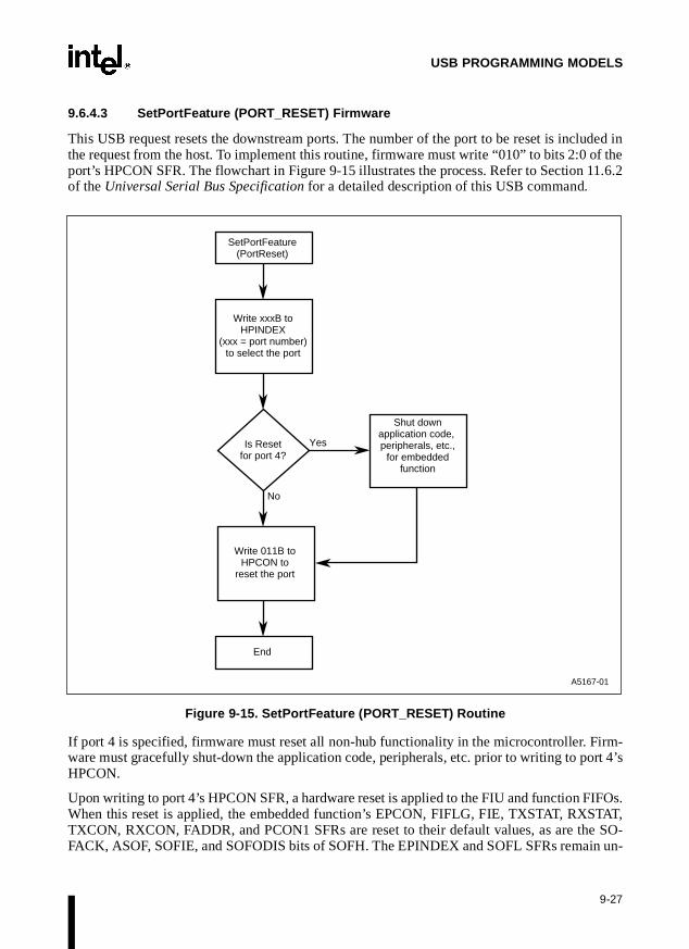
USB PROGRAMMING MODELS
ded inf the1.6.2
rt 4’s
IFOs.TAT,e SO- un-
9.6.4.3 SetPortFeature (PORT_RESET) Firmware
This USB request resets the downstream ports. The number of the port to be reset is incluthe request from the host. To implement this routine, firmware must write “010” to bits 2:0 oport’s HPCON SFR. The flowchart in Figure 9-15 illustrates the process. Refer to Section 1of the Universal Serial Bus Specification for a detailed description of this USB command.
Figure 9-15. SetPortFeature (PORT_RESET) Routine
If port 4 is specified, firmware must reset all non-hub functionality in the microcontroller. Firm-ware must gracefully shut-down the application code, peripherals, etc. prior to writing to poHPCON.
Upon writing to port 4’s HPCON SFR, a hardware reset is applied to the FIU and function FWhen this reset is applied, the embedded function’s EPCON, FIFLG, FIE, TXSTAT, RXSTXCON, RXCON, FADDR, and PCON1 SFRs are reset to their default values, as are thFACK, ASOF, SOFIE, and SOFODIS bits of SOFH. The EPINDEX and SOFL SFRs remain
A5167-01
Write xxxB to HPINDEX
(xxx = port number) to select the port
End
Write 011B to HPCON to
reset the port
Is Reset for port 4?
Shut down application code, peripherals, etc.,
for embedded function
Yes
No
SetPortFeature (PortReset)
9-27

8x930Ax, 8x930Hx USER’S MANUAL
to them-
changed. These SFRs are reset immediately after the write to HPCON, however bus trafficembedded function remains inactive for 15 ms. You may use this time frame to initialize the ebedded function.
9-28

10Input/Output Ports


p-d
ternal
n in-pera-ves theddress
2. Port
CHAPTER 10INPUT/OUTPUT PORTS
The 8x930 has four 8-bit input/output (I/O) ports for general-purpose I/O, external memory oerations, and specific alternate functions (see Table 10-1). This chapter describes the ports anprovides information on port loading, read-modify-write instructions, and external memory ac-cesses. Chapter 16, “External Memory Interface,” contains additional information about exmemory operations.
10.1 INPUT/OUTPUT PORT OVERVIEW
All four 8x930 I/O ports are bidirectional. Each port contains a latch, an output driver, and aput buffer. Port 0 and port 2 output drivers and input buffers facilitate external memory otions. Port 0 drives the lower address byte onto the parallel address bus, and port 2 driupper address byte onto the bus. In nonpage mode, the data is multiplexed with the lower abyte on port 0. In page mode, the data is multiplexed with the upper address byte on port 1 and port 3 provide both general-purpose I/O and special alternate functions.
Table 10-1. Input/Output Port Pin Descriptions
Pin Name Type Alternate
Pin Name Alternate Description Alternate Type
P0.7:0 I/O AD7:0 Address/Data (Nonpage Mode), Address (Page Mode) I/O
P1.0 I/O T2 Timer 2 Clock Input/Output I/O
P1.1 I/O T2EX Timer 2 External Input I
P1.2 I/O ECI PCA External Clock Input I
P1.3 I/O CEX0 PCA Module 0 I/O I/O
P1.4 I/O CEX1 PCA Module 1 I/O I/O
P1.5 I/O CEX2 PCA Module 2 I/O I/O
P1.6 I/O CEX3/WAIT# PCA Module 3 I/O I/O
P1.7 I/O CEX4/A17/WCLK PCA Module 4 I/O or 18th Address Bit I/O(O)
P2.7:0 I/O A15:8 Address (Nonpage Mode), Address/Data (Page Mode) I/O
P3.0 I/O RXD Serial Port Receive Data Input I (I/O)
P3.1 I/O TXD Serial Port Transmit Data Output O (O)
P3.2 I/O INT0# External Interrupt 0 I
P3.3 I/O INT1# External Interrupt 1 I
P3.4 I/O T0 Timer 0 Input I
P3.5 I/O T1 Timer 1 Input I
P3.6 I/O WR# Write Signal to External Memory O
P3.7 I/O RD#/A16 Read Signal to External Memory or 17th Address Bit O
10-1

8x930Ax, 8x930Hx USER’S MANUAL
eadignal” sig-
ourcets al-
e
, shown
10.2 I/O CONFIGURATIONS
Each port SFR operates via type-D latches, as illustrated in Figure 10-1 for ports 1 and 3. A CPU“write to latch” signal initiates transfer of internal bus data into the type-D latch. A CPU “rlatch” signal transfers the latched Q output onto the internal bus. Similarly, a “read pin” stransfers the logical level of the port pin. Some port data instructions activate the “read latchnal while others activate the “read pin” signal. Latch instructions are referred to as read-modify-write instructions (see “Read-Modify-Write Instructions” on page 10-5). Each I/O line may beindependently programmed as input or output.
10.3 PORT 1 AND PORT 3
Figure 10-1 shows the structure of ports 1 and 3, which have internal pullups. An external scan pull the pin low. Each port pin can be configured either for general-purpose I/O or for iternate input or output function (Table 10-1).
To use a pin for general-purpose output, set or clear the corresponding bit in the Px register (x =1, 3). To use a pin for general-purpose input, set the bit in the Px register. This turns off the outputdriver FET.
To configure a pin for its alternate function, set the bit in the Px register. When the latch is set, th“alternate output function” signal controls the output level (Figure 10-1). The operation of ports1 and 3 is discussed further in “Quasi-bidirectional Port Operation” on page 10-5.
10.4 PORT 0 AND PORT 2
Ports 0 and 2 are used for general-purpose I/O or as the external address/data bus. Port 0in Figure 10-2, differs from the other ports in not having internal pullups. Figure 10-3 on page10-4 shows the structure of port 2. An external source can pull a port 2 pin low.
To use a pin for general-purpose output, set or clear the corresponding bit in the Px register (x =0, 2). To use a pin for general-purpose input, set the bit in the Px register to turn off the outputdriver FET.
10-2

INPUT/OUTPUT PORTS
Figure 10-1. Port 1 and Port 3 Structure
Figure 10-2. Port 0 Structure
Read Latch
Read Pin
Write to Latch
Internal Bus
Alternate Output
Function
D
CL
Q
Q#
P3.x Latch
Internal Pullup
P3.x
Alternate Input
Function
A2239-01
VCC
Read Latch
Read Pin
Address/ Data Control
D
CL
Q
Q#
P0.x
A2238-01
VCC
Write to Latch
Internal Bus P0.x
Latch 1
0
10-3

8x930Ax, 8x930Hx USER’S MANUAL
itches
us.
Figure 10-3. Port 2 Structure
When port 0 and port 2 are used for an external memory cycle, an internal control signal swthe output-driver input from the latch output to the internal address/data line. “External MemoryAccess” on page 10-7 discusses the operation of port 0 and port 2 as the external address/data b
NOTEPort 0 and port 2 are precluded from use as general purpose I/O ports when used as address/data bus drivers.
Port 0 internal pullups assist the logic-one output for memory bus cycles only. Except for these bus cycles, the pullup FET is off. All other port 0 outputs are open drain.
Read Latch
Read Pin
Address
Control
D
CL
Q
Q#
P2.x Latch
VCC
Internal Pullup
A2240-01
P2.x
Write to Latch
Internal Bus
1
0
10-4
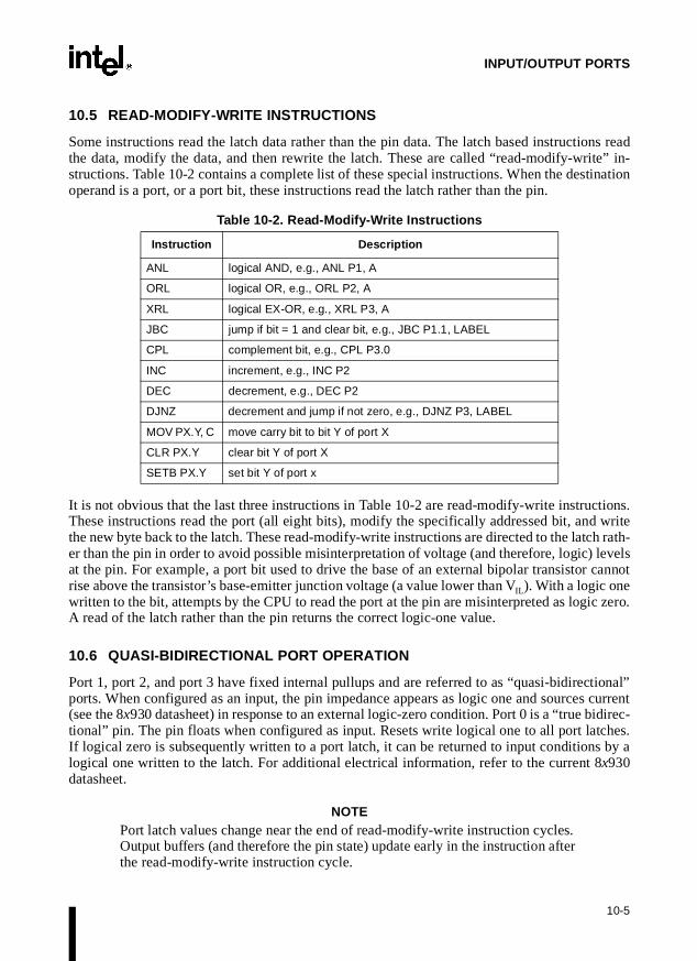
INPUT/OUTPUT PORTS
ns reade” in-ination
writeh rath-levelscannot
c zero.
ional” currentdirec-hes. by a
10.5 READ-MODIFY-WRITE INSTRUCTIONS
Some instructions read the latch data rather than the pin data. The latch based instructiothe data, modify the data, and then rewrite the latch. These are called “read-modify-writstructions. Table 10-2 contains a complete list of these special instructions. When the destoperand is a port, or a port bit, these instructions read the latch rather than the pin.
It is not obvious that the last three instructions in Table 10-2 are read-modify-write instructions.These instructions read the port (all eight bits), modify the specifically addressed bit, andthe new byte back to the latch. These read-modify-write instructions are directed to the latcer than the pin in order to avoid possible misinterpretation of voltage (and therefore, logic) at the pin. For example, a port bit used to drive the base of an external bipolar transistor rise above the transistor’s base-emitter junction voltage (a value lower than VIL). With a logic onewritten to the bit, attempts by the CPU to read the port at the pin are misinterpreted as logiA read of the latch rather than the pin returns the correct logic-one value.
10.6 QUASI-BIDIRECTIONAL PORT OPERATION
Port 1, port 2, and port 3 have fixed internal pullups and are referred to as “quasi-bidirectports. When configured as an input, the pin impedance appears as logic one and sources(see the 8x930 datasheet) in response to an external logic-zero condition. Port 0 is a “true bitional” pin. The pin floats when configured as input. Resets write logical one to all port latcIf logical zero is subsequently written to a port latch, it can be returned to input conditionslogical one written to the latch. For additional electrical information, refer to the current 8x930datasheet.
NOTEPort latch values change near the end of read-modify-write instruction cycles. Output buffers (and therefore the pin state) update early in the instruction after the read-modify-write instruction cycle.
Table 10-2. Read-Modify-Write Instructions
Instruction Description
ANL logical AND, e.g., ANL P1, A
ORL logical OR, e.g., ORL P2, A
XRL logical EX-OR, e.g., XRL P3, A
JBC jump if bit = 1 and clear bit, e.g., JBC P1.1, LABEL
CPL complement bit, e.g., CPL P3.0
INC increment, e.g., INC P2
DEC decrement, e.g., DEC P2
DJNZ decrement and jump if not zero, e.g., DJNZ P3, LABEL
MOV PX.Y, C move carry bit to bit Y of port X
CLR PX.Y clear bit Y of port X
SETB PX.Y set bit Y of port x
10-5

8x930Ax, 8x930Hx USER’S MANUAL
hisurces rath- is onrned on oneT pairssoci-s are
-drain-oneonlyh sinknal
nts to
Logical zero-to-one transitions in port 1, port 2, and port 3 utilize an additional pullup to aid tlogic transition (see Figure 10-4). This increases switch speed. The extra pullup briefly so100 times the normal internal circuit current. The internal pullups are field-effect transistorser than linear resistors. Pullups consist of three p-channel FET (pFET) devices. A pFETwhen the gate senses logical zero and off when the gate senses logical one. pFET #1 is tufor two oscillator periods immediately after a zero-to-one transition in the port latch. A logicat the port pin turns on pFET #3 (a weak pullup) through the inverter. This inverter and pFEform a latch to drive logic one. pFET #2 is a very weak pullup switched on whenever the aated nFET is switched off. This is a traditional CMOS switch convention. Current strength1/10 that of pFET #3.
Figure 10-4. Internal Pullup Configurations
10.7 PORT LOADING
Output buffers of port 1, port 2, and port 3 can each sink 1.6 mA at logic zero (see VOL specifica-tions in the 8x930 data sheet). These port pins can be driven by open-collector and opendevices. Logic zero-to-one transitions occur slowly as limited current pulls the pin to a logiccondition (Figure 10-4 on page 10-6). A logic-zero input turns off pFET #3. This leaves pFET #2 weakly in support of the transition. In external bus mode, port 0 output buffers eac3.2 mA at logic zero (see VOL1 in the 8x930 data sheet). However, the port 0 pins require exterpullups to drive external gate inputs. See the latest revision of the 8x930 datasheet for completeelectrical design information. External circuits must be designed to limit current requiremethese conditions.
Q# From Port
Latch
P3P2P1
n
Port
Input Data
Read Port Pin
2 Osc. Periods
A2242-01
VCCVCCVCC
10-6

INPUT/OUTPUT PORTS
e (usedte ande multi-
ritescles.e port 2
al pull-dance
l pull-
al pull-internalss
al data sig-
strobe
it ad-ry ad-
he in-
10.8 EXTERNAL MEMORY ACCESS
The external bus structure is different for page mode and nonpage mode. In nonpage modby MCS 51 microcontrollers), port 2 outputs the upper address byte; the lower address bythe data are multiplexed on port 0. In page mode, the upper address byte and the data arplexed on port 2, while port 0 outputs the lower address byte.
The 8x930 CPU writes FFH to the P0 register for all external memory bus cycles. This overwprevious information in P0. In contrast, the P2 register is unmodified for external bus cyWhen address bits or data bits are not on the port 2 pins, the bit values in P2 appear on thpins.
In nonpage mode, port 0 uses a strong internal pullup FET to output ones or a strong interndown FET to output zeros for the lower address byte and the data. Port 0 is in a high-impestate for data input.
In page mode, port 0 uses a strong internal pullup FET to output ones or a strong internadown FET to output zeros for the lower address byte or a strong internal pulldown FET to outputzeros for the upper address byte.
In nonpage mode, port 2 uses a strong internal pullup FET to output ones or a strong interndown FET to output zeros for the upper address byte. In page mode, port 2 uses a strong pullup FET to output ones or a strong internal pulldown FET to output zeros for the upper addrebyte and data. Port 2 is in a high-impedance state for data input.
NOTEIn external bus mode port 0 outputs do not require external pullups.
There are two types of external memory accesses: external program memory and externmemory (see Chapter 16, “External Memory Interface”). External program memories utilizenal PSEN# as a read strobe. MCS 51 microcontrollers use RD# (read) or WR# (write) to memory for data accesses. Depending on its RD1:0 configuration bits, the 8x930 uses PSEN# orRD# for data reads (See “Configuration Bits RD1:0” on page 4-8).
During instruction fetches, external program memory can transfer instructions with 16-bdresses for binary-compatible code or with the external bus configured for extended memodressing (17-bit or 18-bit).
External data memory transfers use an 8-, 16-, 17-, or 18-bit address bus, depending on tstruction and the configuration of the external bus. Table 10-3 lists the instructions that can beused for these bus widths.
Table 10-3. Instructions for External Data Moves
Bus Width Instructions
8 MOVX @Ri; MOV @Rm; MOV dir8
16 MOVX @DPTR; MOV @WRj; MOV @WRj+dis; MOV dir16
17 MOV @DRk; MOV @DRk+dis
18 MOV @DRk; MOV @DRk+dis
10-7

8x930Ax, 8x930Hx USER’S MANUAL
ddressrs,driven.
NOTEAvoid MOV P0 instructions for external memory accesses. These instructions can corrupt input code bytes at port 0.
External signal ALE (address latch enable) facilitates external address latch capture. The abyte is valid after the ALE pin drives VOL. For write cycles, valid data is written to port 0 just prioto the write (WR#) pin asserting VOL. Data remains valid until WR# is undriven. For read cycledata returned from external memory must appear at port 0 before the read (RD#) pin is un(refer to the 8x930 datasheet for specifications). Wait states, by definition, affect bus-timing
10-8

11Timer/Counters and Watchdog Timer


herals time,
rupt re-
set if aer”
ed asety ofed sep- capture
)
cribes
TH
r 0 and
he at thed
CHAPTER 11TIMER/COUNTERS AND WATCHDOG TIMER
This chapter describes the timer/counters and the watchdog timer (WDT) included as peripon the 8x930. When operating as a timer, a timer/counter runs for a programmed length ofthen issues an interrupt request. When operating as a counter, a timer/counter counts negativetransitions on an external pin. After a preset number of counts, the counter issues an interquest.
The watchdog timer provides a way to monitor system operation. It causes a system refirmware malfunction allows it to expire. The watchdog timer is covered in “Watchdog Timon page 11-16.
11.1 TIMER/COUNTER OVERVIEW
The 8x930 contains three general-purpose, 16-bit timer/counters. Although they are identifitimer 0, timer 1, and timer 2, you can independently configure each to operate in a varimodes as a timer or as an event counter. Each timer employs two 8-bit timer registers, usarately or in cascade, to maintain the count. The timer registers and associated control andregisters are implemented as addressable special function registers (SFRs). Four of the SFRs pro-vide programmable control of the timers as follows:
• Timer/counter mode control register (TMOD) and timer/counter control register (TCONcontrol timer 0 and timer 1
• Timer/counter 2 mode control register (T2MOD) and timer/counter 2 control register (T2CON) control timer 2
Table 11-1 describes the external signals referred to in this chapter. Table 11-2 briefly desthe SFRs referred to in this chapter. For a map of the SFR address space, see Table 3-5 on page3-16.
11.2 TIMER/COUNTER OPERATION
The block diagram in Figure 11-1 depicts the basic logic of the timers. Here timer registersxand TLx (x = 0, 1, and 2) connect in cascade to form a 16-bit timer. Setting the run control bit(TRx) turns the timer on by allowing the selected input to increment TLx. When TLx overflowsit increments THx; when THx overflows it sets the timer overflow flag (TFx) in the TCON orT2CON register. Setting the run control bit does not clear the THx and TLx timer registers. Thetimer registers can be accessed to obtain the current count or to enter preset values. Timetimer 1 can also be controlled by external pin INTx# to facilitate pulse width measurements.
The C\Tx# control bit selects timer operation or counter operation by selecting the divided-downsystem clock or external pin Tx as the source for the counted signal.
For timer operation (C/Tx# = 0), the timer register counts the divided-down system clock. Ttimer register is incremented once every peripheral cycle (once every six states). That is,internal clock frequency divided by six (FCLK/6). Exceptions are the timer 2 clock-out and bau
11-1

8x930Ax, 8x930Hx USER’S MANUAL
1
Unit” high in
ipheral
led at
rate modes, in which the timer register is incremented at the internal clock rate (FCLK). See “Clockand Reset Unit” on page 2-9. Table 2-4 on page 2-10 and Figures 2-7, and 2-8 on page 2-1showthe relationship between FOSC, FCLK, state times, and peripheral cycles. Also see the 8x930 clockcircuit block diagram in Figure 2-6 on page 2-9.
NOTEThe timing calculations in this chapter are based on the value of FCLK, which is a function of PLLSEL2:0. See Table 2-4 on page 2-10.
For counter operation (C/Tx# = 1), the timer register counts the negative transitions on the Tx ex-ternal input pin. The external input is sampled during every S5P2 state. “Clock and Reseton page 2-9 describes the notation for the states in a peripheral cycle. When the sample isone cycle and low in the next, the counter is incremented. The new count value appears in theregister during the next S3P1 state after the transition was detected. Since it takes two percycles to recognize a negative transition, the maximum count rate is FCLK/12. There are no restric-tions on the duty cycle of the external input signal, but to ensure that a given level is sampleast once before it changes, it should be held for at least one full peripheral cycle.
Table 11-1. External Signals
SignalName Type Description Alternate
Function
T2 I/O Timer 2 Clock Input/Output . This signal is the external clock input for the timer 2 capture mode; and it is the timer 2 clock-output for the clock-out mode.
P1.0
T2EX I Timer 2 External Input . In timer 2 capture mode, a falling edge initiates a capture of the timer 2 registers. In auto-reload mode, a falling edge causes the timer 2 registers to be reloaded. In the up-down counter mode, this signal determines the count direction: high = up, low = down.
P1.1
INT1:0# I External Interrupts 1:0 . These inputs set the IE1:0 interrupt flags in the TCON register. TCON bits IT1:0 select the triggering method:IT1:0 = 1 selects edge-triggered (high-to-low);IT1:0 = 0 selects level-triggered (active low). INT1:0# also serves as external run control for timer 1:0 when selected by TCON bits GATE1:0#.
P3.3:2
T1:0 I Timer 1:0 External Clock Inputs . When timer 1:0 operates as a counter, a falling edge on the T1:0 pin increments the count.
P3.5:4
11-2

TIMER/COUNTERS AND WATCHDOG TIMER
Figure 11-1. Basic Logic of the Timer/Counters
Table 11-2. Timer/ Counter and Watchdog Timer SFRs
Mnemonic Description Address
TL0TH0
Timer 0 Timer Registers. Used separately as 8-bit counters or in cascade as a 16-bit counter. Counts an internal clock signal with frequency FCLK/6 (timer operation) or an external input (event counter operation).
S:8AHS:8CH
TL1TH1
Timer 1 Timer Registers. Used separately as 8-bit counters or in cascade as a 16-bit counter. Counts an internal clock signal with frequency FCLK/6 (timer operation) or an external input (event counter operation).
S:8BHS:8DH
TL2TH2
Timer 2 Timer Registers. TL2 and TH2 connect in cascade to provide a 16-bit counter. Counts an internal clock signal with frequency FCLK/6 (timer operation) or an external input (event counter operation).
S:CCHS:CDH
TCON Timer 0/1 Control Register. Contains the run control bits, overflow flags, interrupt flags, and interrupt-type control bits for timer 0 and timer 1.
S:88H
TMOD Timer 0/1 Mode Control Register. Contains the mode select bits, counter/timer select bits, and external control gate bits for timer 0 and timer 1.
S:89H
T2CON Timer 2 Control Register. Contains the receive clock, transmit clock, and capture/reload bits used to configure timer 2. Also contains the run control bit, counter/timer select bit, overflow flag, external flag, and external enable for timer 2.
S:C8H
T2MOD Timer 2 Mode Control Register. Contains the timer 2 output enable and down count enable bits.
S:C9H
RCAP2LRCAP2H
Timer 2 Reload/Capture Registers (RCAP2L, RCAP2H). Provide values to and receive values from the timer registers (TL2,TH2).
S:CAHS:CBH
WDTRST Watchdog Timer Reset Register (WDTRST). Used to reset and enable the WDT.
S:A6H
A5197-01
TRx
TLx (8 Bits)
THx (8 Bits) TFx
Interrupt Request
6
Tx
Overflow
x = 0, 1, or 2
FCLK
C/Tx#
0
1
11-3

8x930Ax, 8x930Hx USER’S MANUAL
11-2,
5, 4,r gat- Theter-
e se-Thison page
rrupt
with. Theerflow
igure
11.3 TIMER 0
Timer 0 functions as either a timer or event counter in four modes of operation. Figures11-3, and 11-4 show the logical configuration of each mode.
Timer 0 is controlled by the four low-order bits of the TMOD register (Figure 11-5) and bits 1, and 0 of the TCON register (Figure 11-6). The TMOD register selects the method of timeing (GATE0), timer or counter operation (T/C0#), and mode of operation (M10 and M00).TCON register provides timer 0 control functions: overflow flag (TF0), run control (TR0), inrupt flag (IE0), and interrupt type control (IT0).
For normal timer operation (GATE0 = 0), setting TR0 allows TL0 to be incremented by thlected input. Setting GATE0 and TR0 allows external pin INT0# to control timer operation. setup can be used to make pulse width measurements. See “Pulse Width Measurements” 11-10.
Timer 0 overflow (count rolls over from all 1s to all 0s) sets the TF0 flag generating an interequest.
11.3.1 Mode 0 (13-bit Timer)
Mode 0 configures timer 0 as a 13-bit timer which is set up as an 8-bit timer (TH0 register)a modulo 32 prescalar implemented with the lower five bits of the TL0 register (Figure 11-2)upper three bits of the TL0 register are indeterminate and should be ignored. Prescalar ovincrements the TH0 register.
11.3.2 Mode 1 (16-bit Timer)
Mode 1 configures timer 0 as a 16-bit timer with TH0 and TL0 connected in cascade (F11-2). The selected input increments TL0.
Figure 11-2. Timer 0/1 in Mode 0 and Mode 1
A5198-01
GATEx
INTx#
TRx
TLx (8 Bits)
THx (8 Bits) TFx
Interrupt Request
6
Tx
Overflow
Mode 0: 13-bit Timer/Counter Mode 1: 16-bit Timer/Counter x = 0 or 1
FCLK
C/Tx#
0
1
11-4

TIMER/COUNTERS AND WATCHDOG TIMER
thestert re-
ad Set-
s (Fig-nter.N inf
Halt)”
11.3.3 Mode 2 (8-bit Timer With Auto-reload)
Mode 2 configures timer 0 as an 8-bit timer (TL0 register) that automatically reloads fromTH0 register (Figure 11-3). TL0 overflow sets the timer overflow flag (TF0) in the TCON regiand reloads TL0 with the contents of TH0, which is preset by firmware. When the interrupquest is serviced, hardware clears TF0. The reload leaves TH0 unchanged. See “Auto-reloup Example” on page 11-9.
Figure 11-3. Timer 0/1 in Mode 2, Auto-reload
11.3.4 Mode 3 (Two 8-bit Timers)
Mode 3 configures timer 0 such that registers TL0 and TH0 operate as separate 8-bit timerure 11-4). This mode is provided for applications requiring an additional 8-bit timer or couTL0 uses the timer 0 control bits C/T0# and GATE0 in TMOD, and TR0 and TF0 in TCOthe normal manner. TH0 is locked into a timer function (counting FCLK /6) and takes over use othe timer 1 interrupt (TF1) and run control (TR1) bits. Thus, operation of timer 1 is restrictedwhen timer 0 is in mode 3. See the last paragraph of “Timer 1” on page 11-6 and “Mode 3 (on page 11-9.
A5199-01
GATEx
INTx#
TRx
TLx (8 Bits) TFx
Interrupt Request
6
Tx
Overflow
x = 0 or 1
FCLK
Reload
THx (8 Bits)
C/Tx#
0
1
11-5

8x930Ax, 8x930Hx USER’S MANUAL
-2 andode.
7, timer. Theter-
ud rate
ent-r op-Width
rrupt
Forud rated on.
Figure 11-4. Timer 0 in Mode 3, Two 8-bit Timers
11.4 TIMER 1
Timer 1 functions as either a timer or event counter in three modes of operation. Figures 1111-3 show the logical configuration for modes 0, 1, and 2. Timer 1’s mode 3 is a hold-count m
Timer 1 is controlled by the four high-order bits of the TMOD register (Figure 11-5) and bits6, 3, and 2 of the TCON register (Figure 11-6). The TMOD register selects the method ofgating (GATE1), timer or counter operation (T/C1#), and mode of operation (M11 and M01)TCON register provides timer 1 control functions: overflow flag (TF1), run control (TR1), inrupt flag (IE1), and interrupt type control (IT1).
Timer 1 operation in modes 0, 1, and 2 is identical to timer 0. Timer 1 can serve as the bagenerator for the serial port. Mode 2 is best suited for this purpose.
For normal timer operation (GATE1 = 0), setting TR1 allows timer register TL1 to be incremed by the selected input. Setting GATE1 and TR1 allows external pin INT1# to control timeeration. This setup can be used to make pulse width measurements. See “Pulse Measurements” on page 11-10.
Timer 1 overflow (count rolls over from all 1s to all 0s) sets the TF1 flag, generating an interequest.
When timer 0 is in mode 3, it uses timer 1’s overflow flag (TF1) and run control bit (TR1).this situation, use timer 1 only for applications that do not require an interrupt (such as a bagenerator for the serial interface port) and switch timer 1 in and out of mode 3 to turn it off an
A5200-01
GATE0
INT0#
TR0
TL0 (8 Bits) TF0
Interrupt Request
6
T0
Overflow
FCLK TF1OverflowTH0
(8 Bits)
TR1
Interrupt Request
C/T0#
0
1
11-6

TIMER/COUNTERS AND WATCHDOG TIMER
Figure 11-5. TMOD: Timer/Counter Mode Control Register
TMOD Address: S:89HReset State: 0000 0000B
Timer/Counter Mode Control Register. Contains mode select, run control select, and counter/timer select bits for controlling timer 0 and timer 1.
7 0
GATE1 C/T1# M11 M01 GATE0 C/T0# M10 M00
Bit Number
Bit Mnemonic Function
7 GATE1 Timer 1 Gate:
When GATE1 = 0, run control bit TR1 gates the input signal to the timer register. When GATE1 = 1 and TR1 = 1, external signal INT1 gates the timer input.
6 C/T1# Timer 1 Counter/Timer Select:
C/T1# = 0 selects timer operation: timer 1 counts the divided-down system clock. C/T1# = 1 selects counter operation: timer 1 counts negative transitions on external pin T1.
5, 4 M11, M01 Timer 1 Mode Select:
M11 M010 0 Mode 0: 8-bit timer/counter (TH1) with 5-bit prescalar (TL1)0 1 Mode 1: 16-bit timer/counter1 0 Mode 2: 8-bit auto-reload timer/counter (TL1). Reloaded
from TH1 at overflow.1 1 Mode 3: Timer 1 halted. Retains count.
3 GATE0 Timer 0 Gate:
When GATE0 = 0, run control bit TR0 gates the input signal to the timer register. When GATE0 = 1 and TR0 = 1, external signal INT0 gates the timer input.
2 C/T0# Timer 0 Counter/Timer Select:
C/T0# = 0 selects timer operation: timer 0 counts the divided-down system clock. C/T0# = 1 selects counter operation: timer 0 counts negative transitions on external pin T0.
1, 0 M10, M00 Timer 0 Mode Select:
M10 M000 0 Mode 0: 8-bit timer/counter (T0) with 5-bit prescalar (TL0)0 1 Mode 1: 16-bit timer/counter1 0 Mode 2: 8-bit auto-reload timer/counter (TL0). Reloaded
from TH0 at overflow.1 1 Mode 3: TL0 is an 8-bit timer/counter. TH0 is an 8-bit
timer using timer 1’s TR1 and TF1 bits.
11-7

8x930Ax, 8x930Hx USER’S MANUAL
Figure 11-6. TCON: Timer/Counter Control Register
TCON Address: S:88HReset State: 0000 0000B
Timer/Counter Control Register. Contains the overflow and external interrupt flags and the run control and interrupt transition select bits for timer 0 and timer 1.
7 0
TF1 TR1 TF0 TR0 IE1 IT1 IE0 IT0
Bit Number
Bit Mnemonic Function
7 TF1 Timer 1 Overflow Flag:
Set by hardware when the timer 1 register overflows. Cleared by hardware when the processor vectors to the interrupt routine.
6 TR1 Timer 1 Run Control Bit:
Set/cleared by firmware to turn timer 1 on/off.
5 TF0 Timer 0 Overflow Flag:
Set by hardware when the timer 0 register overflows. Cleared by hardware when the processor vectors to the interrupt routine.
4 TR0 Timer 0 Run Control Bit:
Set/cleared by firmware to turn timer 1 on/off.
3 IE1 Interrupt 1 Flag:
Set by hardware when an external interrupt is detected on the INT1# pin. Edge- or level- triggered (see IT1). Cleared when interrupt is processed if edge-triggered.
2 IT1 Interrupt 1 Type Control Bit:
Set this bit to select edge-triggered (high-to-low) for external interrupt 1.Clear this bit to select level-triggered (active low).
1 IE0 Interrupt 0 Flag:
Set by hardware when an external interrupt is detected on the INT0# pin. Edge- or level- triggered (see IT0). Cleared when interrupt is processed if edge-triggered.
0 IT0 Interrupt 0 Type Control Bit:
Set this bit to select edge-triggered (high-to-low) for external interrupt 0.Clear this bit to select level-triggered (active low).
11-8

TIMER/COUNTERS AND WATCHDOG TIMER
) with. Theister.
igure
TH1eg-aves
imer 1 para-
er-xamplesers.
he
r
11.4.1 Mode 0 (13-bit Timer)
Mode 0 configures timer 0 as a 13-bit timer, which is set up as an 8-bit timer (TH1 registera modulo-32 prescalar implemented with the lower five bits of the TL1 register (Figure 11-2)upper three bits of the TL1 register are ignored. Prescalar overflow increments the TH1 reg
11.4.2 Mode 1 (16-bit Timer)
Mode 1 configures timer 1 as a 16-bit timer with TH1 and TL1 connected in cascade (F11-2). The selected input increments TL1.
11.4.3 Mode 2 (8-bit Timer with Auto-reload)
Mode 2 configures timer 1 as an 8-bit timer (TL1 register) with automatic reload from the register on overflow (Figure 11-3). Overflow from TL1 sets overflow flag TF1 in the TCON rister and reloads TL1 with the contents of TH1, which is preset by firmware. The reload leTH1 unchanged. See “Auto-reload Setup Example” on page 11-9.
11.4.4 Mode 3 (Halt)
Placing timer 1 in mode 3 causes it to halt and hold its count. This can be used to halt twhen the TR1 run control bit is not available (i.e., when timer 0 is in mode 3). See the finalgraph of “Timer 1” on page 11-6.
11.5 TIMER 0/1 APPLICATIONS
Timer 0 and timer 1 are general purpose timers that can be used in a variety of ways. The timapplications presented in this section are intended to demonstrate timer setup, and do not represent the only arrangement nor necessarily the best arrangement for a given task. These eemploy timer 0, but timer 1 can be set up in the same manner using the appropriate regist
11.5.1 Auto-reload Setup Example
Timer 0 can be configured as an eight-bit timer (TL0) with automatic reload as follows:
1. Program the four low-order bits of the TMOD register (Figure 11-5) to specify: mode 2 for timer 0, C/T0# = 0 to select FCLK/6 as the timer input, and GATE0 = 0 to select TR0 as ttimer run control.
2. Enter an eight-bit initial value (n0) in timer register TL0, so that the timer overflows aftethe desired number of peripheral cycles.
3. Enter an eight-bit reload value (nR) in register TH0. This can be the same as n0 or different, depending on the application.
4. Set the TR0 bit in the TCON register (Figure 11-6) to start the timer. Timer overflow occurs after FFH + 1 - n0 peripheral cycles, setting the TF0 flag and loading nR into TL0 from TH0. When the interrupt is serviced, hardware clears TF0.
11-9

8x930Ax, 8x930Hx USER’S MANUAL
pulsellows:
re
m is
nd
-nd
e. Set-
TF2
5. The timer continues to overflow and generate interrupt requests every FFH + 1 - nR peripheral cycles.
6. To halt the timer, clear the TR0 bit.
11.5.2 Pulse Width Measurements
For timer 0 and timer 1, setting GATEx and TRx allows an external waveform at pin INTx# toturn the timer on and off. This setup can be used to measure the width of a positive-goingpresent at pin INTx#. Pulse width measurements using timer 0 in mode 1 can be made as fo
1. Program the four low-order bits of the TMOD register (Figure 11-5) to specify: mode 1 for timer 0, C/T0# = 0 to select FCLK/6 as the timer input, and GATE0 = 1 to select INT0 astimer run control.
2. Enter an initial value of all zeros in the 16-bit timer register TH0/TL0, or read and stothe current contents of the register.
3. Set the TR0 bit in the TCON register (Figure 11-6) to enable INT0.
4. Apply the pulse to be measured to pin INT0. The timer runs when the pulse waveforhigh.
5. Clear the TR0 bit to disable INT0.
6. Read timer register TH0/TL0 to obtain the new value.
7. Calculate pulse width = 6TCLK × (new value - initial value).
8. Example 1, PLLSEL2:0 = 100 (low speed): FOSC = 12 MHz, FCLK = 6 MHz, TCLK = 0.16667 µs. If the new value = 10,00010 counts and the initial value = 0, the pulsewidth = 6(0.16667) x (10,000 – 0) = 1 µs × 10,000 = 10 ms.
Example 2, PLLSEL2:0 = 110 (full speed): FOSC = 12 MHz, FCLK = 12 MHz, TCLK = 0.08333 µs. If the new value = 10,00010 counts and the initial value = 0, the pulsewidth = 6(0.08333) x (10,000 – 0) = 0.5 µs × 10,000 = 5 ms.
11.6 TIMER 2
Timer 2 is a 16-bit timer/counter. The count is maintained by two 8-bit timer registers, TH2 aTL2, connected in cascade. The timer/counter 2 mode control register (T2MOD) as shown in Fig-ure 11-11 on page 11-16) and the timer/counter 2 control register (T2CON) as shown in Figure11-12 on page 11-17) control the operation of timer 2.
Timer 2 provides the following operating modes: capture mode, auto-reload mode, baud rate generator mode, and programmable clock-out mode. Select the operating mode with T2MOD aTCON register bits as shown in Table 11-3 on page 11-15. Auto-reload is the default modting RCLK and/or TCLK selects the baud rate generator mode.
Timer 2 operation is similar to timer 0 and timer 1. C/T2# selects the divided-down system clock(timer operation) or external pin T2 (counter operation) as the timer register input. Settingallows TL2 to be incremented by the selected input.
11-10
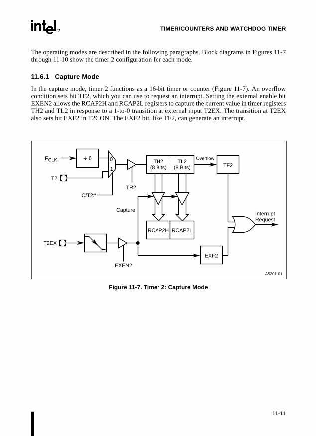
TIMER/COUNTERS AND WATCHDOG TIMER
s 11-7
rflowble bitisters2EX
The operating modes are described in the following paragraphs. Block diagrams in Figurethrough 11-10 show the timer 2 configuration for each mode.
11.6.1 Capture Mode
In the capture mode, timer 2 functions as a 16-bit timer or counter (Figure 11-7). An ovecondition sets bit TF2, which you can use to request an interrupt. Setting the external enaEXEN2 allows the RCAP2H and RCAP2L registers to capture the current value in timer regTH2 and TL2 in response to a 1-to-0 transition at external input T2EX. The transition at Talso sets bit EXF2 in T2CON. The EXF2 bit, like TF2, can generate an interrupt.
Figure 11-7. Timer 2: Capture Mode
Interrupt Request
T2EX
TF26
T2
Overflow
RCAP2H
TR2
RCAP2L
TH2 (8 Bits)
EXEN2
EXF2
Capture
A5201-01
FCLK
C/T2#
0
1TL2
(8 Bits)
11-11

8x930Ax, 8x930Hx USER’S MANUAL
eload.
timer
XEN2p toe re-n
tran-ither
11.6.2 Auto-reload Mode
The auto-reload mode configures timer 2 as a 16-bit timer or event counter with automatic rThe timer operates an as an up counter or as an up/down counter, as determined by the downcounter enable bit (DCEN). At device reset, DCEN is cleared, so in the auto-reload mode,2 defaults to operation as an up counter.
11.6.2.1 Up Counter Operation
When DCEN = 0, timer 2 operates as an up counter (Figure 11-8). The external enable bit Ein the T2CON register provides two options (Figure 11-12). If EXEN2 = 0, timer 2 counts uFFFFH and sets the TF2 overflow flag. The overflow condition loads the 16-bit value in thload/capture registers (RCAP2H, RCAP2L) into the timer registers (TH2, TL2). The values iRCAP2H and RCAP2L are preset by firmware.
If EXEN2 = 1, the timer registers are reloaded by either a timer overflow or a high-to-low sition at external input T2EX. This transition also sets the EXF2 bit in the T2CON register. ETF2 or EXF2 bit can generate a timer 2 interrupt request.
Figure 11-8. Timer 2: Auto-reload Mode (DCEN = 0)
Interrupt Request
T2EX
TF2
6
T2
Overflow
TR2
TH2 (8 Bits)
TL2 (8 Bits)
EXEN2
EXF2
Reload
A5202-01
FCLK
RCAP2H RCAP2L
C/T2#
0
1
11-12

TIMER/COUNTERS AND WATCHDOG TIMER
con-ts up.es an load-
imere
ount. bit can
11.6.3 Up/Down Counter Operation
When DCEN = 1, timer 2 operates as an up/down counter (Figure 11-9). External pin T2EXtrols the direction of the count (Table 11-1 on page 11-2). When T2EX is high, timer 2 counThe timer overflow occurs at FFFFH which sets the timer 2 overflow flag (TF2) and generatinterrupt request. The overflow also causes the 16-bit value in RCAP2H and RCAP2L to beed into the timer registers TH2 and TL2.
When T2EX is low, timer 2 counts down. Timer underflow occurs when the count in the tregisters (TH2, TL2) equals the value stored in RCAP2H and RCAP2L. The underflow sets thTF2 bit and reloads FFFFH into the timer registers.
The EXF2 bit toggles when timer 2 overflows or underflows, changing the direction of the cWhen timer 2 operates as an up/down counter, EXF2 does not generate an interrupt. Thisbe used to provide 17-bit resolution.
Figure 11-9. Timer 2: Auto-reload Mode (DCEN = 1)
Interrupt Request
T2
Overflow
TR2
TH2 (8 Bits)
TL2 (8 Bits)
FFH FFH
6
T2EX
Count Direction 1 = Up 0 = Down
TF2
EXF2
Toggle
(Down Counting Reload Value)
(Up Counting Reload Value)
RCAP2LRCAP2H
A5203-01
FCLK
C/T2#
0
1
11-13

8x930Ax, 8x930Hx USER’S MANUAL
s mode this
igurethe in-ue.Inquen-
ge-
e
2L
oad
er 2 asd rates
11.6.4 Baud Rate Generator Mode
This mode configures timer 2 as a baud rate generator for use with the serial port. Select thiby setting the RCLK and/or TCLK bits in T2CON. See Table 11-3. For details regardingmode of operation, refer to “Baud Rates” on page 13-10.
11.6.5 Clock-out Mode
In the clock-out mode, timer 2 functions as a 50%-duty-cycle, variable-frequency clock (F11-10). The generated clock signal appears on pin T2. The input clock increments TL0 at ternal clock frequency (FCLK). The timer repeatedly counts to overflow from a preloaded valAt overflow, the contents of the RCAP2H and RCAP2L registers are loaded into TH2/TL2. this mode, timer 2 overflows do not generate interrupts. The formula gives the clock-out frecy as a function of FCLK (Table 2-4 on page 2-10) and the value in the RCAP2H and RCAP2Lregisters:
For PLLSEL2:0 = 100 (low speed, FCLK = 6 MHz), timer 2 has a programmable frequency ranof 45.8 Hz to 3 MHz. For PLLSEL2:0 = 110 (full speed, FCLK = 12 MHz), timer 2 has a programmable frequency range of 91.6 Hz to 6 MHz.
Timer 2 is programmed for the clock-out mode as follows:
1. Set the T2OE bit in T2MOD. This gates the timer register overflow to the ÷2 counter.
2. Clear the C/T2# bit in T2CON to select FCLK as the timer input signal. This also gates thoutput of the ÷2 counter to pin T2.
3. Determine the 16-bit reload value from the formula and enter in the RCAP2H/RCAPregisters.
4. Enter a 16-bit initial value in timer register TH2/TL2. This can be the same as the relvalue, or different, depending on the application.
5. To start the timer, set the TR2 run control bit in T2CON.
Operation is similar to timer 2 operation as a baud rate generator. It is possible to use tima baud rate generator and a clock generator simultaneously. For this configuration, the bauand clock frequencies are not independent since both functions use the values in the RCAP2Hand RCAP2L registers.
Clock-out FrequencyFCLK
2 (65535 - RCAP2H, RCAP2L)×--------------------------------------------------------------------------------------=
11-14

TIMER/COUNTERS AND WATCHDOG TIMER
Figure 11-10. Timer 2: Clock Out Mode
.
Table 11-3. Timer 2 Modes of Operation
Mode RCLK OR TCLK(in T2CON)
CP/RL2#(in T2 CON)
T2OE(in T2MOD)
Auto-reload Mode 0 0 0
Capture Mode 0 1 0
Baud Rate Generator Mode 1 X X
Programmable Clock-Out X 0 1
Interrupt Request
T2EX
T2OE
RCAP2H
TR2
RCAP2L
TH2 (8 Bits)
EXEN2
EXF2
TL2 (8 Bits)
2
A5204-01
T2
C/T2#
0
1
FCLK
11-15

8x930Ax, 8x930Hx USER’S MANUAL
ering de-
ted in
ontrol
T.
For µs
read
Figure 11-11. T2MOD: Timer 2 Mode Control Register
11.7 WATCHDOG TIMER
The peripheral section of the 8x930 contains a dedicated, hardware watchdog timer (WDT) thatautomatically resets the chip if it is allowed to time out. The WDT provides a means of recovfrom routines that do not complete successfully due to firmware malfunctions. The WDTscribed in this section is not associated with the PCA watchdog timer, which is implemenfirmware.
11.7.1 Description
The WDT is a 14-bit counter that counts peripheral cycles, i.e., (FCLK/6. The WDTRST specialfunction register at address S:A6H provides control access to the WDT. Two operations cthe WDT:
• Device reset clears and disables the WDT (see “Reset” on page 14-5).
• Writing a specific two-byte sequence to the WDTRST register clears and enables the WD
If it is not cleared, the WDT overflows on count 3FFFH + 1. For PLLSEL2:0 = 100 (FCLK = 6MHZ, a peripheral cycle is 1 µs), the WDT overflows in 1 µs × 16384 = 16.384 ms.PLLSEL2:0 = 110 (FCLK = 12 MHZ, a peripheral cycle is 0.5 µs), the WDT overflows in 0.5× 16384 = 8.192 ms.
The WDTRST is a write-only register. Attempts to read it return FFH. The WDT itself is not or write accessible. The WDT does not drive the external RESET pin.
T2MOD Address: S:C9HReset State: xxxx xx00B
Timer 2 Mode Control Register. Contains the timer 2 down count enable and clock-out enable bits for timer 2 .
7 0
— — — — — — T2OE DCEN
Bit Number
Bit Mnemonic Function
7:2 — Reserved:
Values read from these bits are indeterminate. Write zeros to these bits.
1 T2OE Timer 2 Output Enable Bit:
In the timer 2 clock-out mode, connects the programmable clock output to external pin T2.
0 DCEN Down Count Enable Bit:
Configures timer 2 as an up/down counter.
11-16

TIMER/COUNTERS AND WATCHDOG TIMER
Figure 11-12. T2CON: Timer 2 Control Register
T2CON Address: S:C8HReset State: 0000 0000B
Timer 2 Control Register. Contains the receive clock, transmit clock, and capture/reload bits used to configure timer 2. Also contains the run control bit, counter/timer select bit, overflow flag, external flag, and external enable for timer 2.
7 0
TF2 EXF2 RCLK TCLK EXEN2 TR2 C/T2# CP/RL2#
Bit Number
Bit Mnemonic Function
7 TF2 Timer 2 Overflow Flag:
Set by timer 2 overflow. Must be cleared by firmware. TF2 is not set if RCLK = 1 or TCLK = 1.
6 EXF2 Timer 2 External Flag:
If EXEN2 = 1, capture or reload caused by a negative transition on T2EX sets EFX2. EXF2 does not cause an interrupt in up/down counter mode (DCEN = 1).
5 RCLK Receive Clock Bit:
Selects timer 2 overflow pulses (RCLK = 1) or timer 1 overflow pulses (RCLK = 0) as the baud rate generator for serial port modes 1 and 3.
4 TCLK Transmit Clock Bit:
Selects timer 2 overflow pulses (TCLK = 1) or timer 1 overflow pulses (TCLK = 0) as the baud rate generator for serial port modes 1 and 3.
3 EXEN2 Timer 2 External Enable Bit:
Setting EXEN2 causes a capture or reload to occur as a result of a negative transition on T2EX unless timer 2 is being used as the baud rate generator for the serial port. Clearing EXEN2 causes timer 2 to ignore events at T2EX.
2 TR2 Timer 2 Run Control Bit:
Setting this bit starts the timer.
1 C/T2# Timer 2 Counter/Timer Select:
C/T2# = 0 selects timer operation: timer 2 counts the divided-down system clock. C/T2# = 1 selects counter operation: timer 2 counts negative transitions on external pin T2.
0 CP/RL2# Capture/Reload Bit:
When set, captures occur on negative transitions at T2EX if EXEN2 = 1. When cleared, auto-reloads occur on timer 2 overflows or negative transitions at T2EX if EXEN2 = 1. The CP/RL2# bit is ignored and timer 2 forced to auto-reload on timer 2 overflow, if RCLK = 1 or TCLK = 1.
11-17

8x930Ax, 8x930Hx USER’S MANUAL
er to
-E1H
WDTice thet whenheral
to holdated
if the
11.7.2 Using the WDT
To use the WDT to recover from system malfunctions, the user program should control the WDTas follows:
1. Following device reset, write the two-byte sequence 1EH-E1H to the WDTRST registenable the WDT. The WDT begins counting from 0.
2. Repeatedly for the duration of program execution, write the two-byte sequence 1EHto the WDTRST register to clear and enable the WDT before it overflows. The WDT starts over at 0.
If the WDT overflows, it initiates a device reset (see “Reset” on page 14-5). Device reset clearsthe WDT and disables it.
11.7.3 WDT During Idle Mode
Operation of the WDT during the power reduction modes deserves special attention. Thecontinues to count while the microcontroller is in idle mode. This means the user must servWDT during idle. One approach is to use a peripheral timer to generate an interrupt requesthe timer overflows. The interrupt service routine then clears the WDT, reloads the periptimer for the next service period, and puts the microcontroller back into idle.
11.7.4 WDT During PowerDown
The powerdown mode stops all phase clocks. This causes the WDT to stop counting and its count. The WDT resumes counting from where it left off if the powerdown mode is terminby INT0/INT1. To ensure that the WDT does not overflow shortly after exiting the powerdownmode, clear the WDT just before entering powerdown. The WDT is cleared and disabledpowerdown mode is terminated by a reset.
11-18
12Programmable Counter Array


8tion
com-r for theit bus.hile
ister
e Tablections.
ed byt com-
or. Thepture in the tim-
CHAPTER 12PROGRAMMABLE COUNTER ARRAY
This chapter describes the programmable counter array (PCA), an on-chip peripheral of thex930that performs a variety of timing and counting operations, including pulse width modula(PWM). The PCA provides the capability for a firmware watchdog timer (WDT).
12.1 PCA DESCRIPTION
The programmable counter array (PCA) consists of a 16-bit timer/counter and five 16-bit pare/capture modules. The timer/counter serves as a common time base and event countecompare/capture modules, distributing the current count to the modules by means of a 16-bA special function register (SFR) pair, CH/CL, maintains the count in the timer/counter, wfive SFR pairs, CCAPxH/CCAPxL, store values for the modules (see Figure 12-1). AdditionalSFRs provide control and mode select functions as follows:
• The PCA timer/counter mode register (CMOD) and the PCA timer/counter control reg(CCON) control the operation of the timer/counter. See Figure 12-7 on page 12-13 and Figure 12-8 on page 12-14.
• Five PCA module mode registers (CCAPMx) specify the operating modes of the compare/capture modules. See Figure 12-9 on page 12-16.
For a list of SFRs associated with the PCA, see Table 12-1. For an SFR address map, se3-5 on page 3-16. Port 1 provides external I/O for the PCA on a shared basis with other funTable 12-2 identifies the port pins associated with the timer/counter and compare/capture mod-ules. When not used for PCA I/O, these pins can be used for standard I/O functions.
The operating modes of the five compare/capture modules determine the functions performthe PCA. Each module can be independently programmed to provide input capture, outpupare, or pulse width modulation. Module 4 only also has a watchdog-timer mode.
The PCA timer/counter and the five compare/capture modules share a single interrupt vectEC bit in the IEN0 special function register is a global interrupt enable for the PCA. Caevents, compare events in some modes, and PCA timer/counter overflows all set flagsCCON register. Setting the overflow flag (CF) generates a PCA interrupt request if the PCAer/counter interrupt enable bit (ECF) in the CMOD register is set (Figure 12-1). Setting a com-pare/capture flag (CCFx) generates a PCA interrupt request if the ECCFx interrupt enable bit inthe corresponding CCAPMx register is set (Figures 12-2 and 12-3). For a description of the 8x930interrupt system see Chapter 6, “Interrupt System”.
12-1
8x930Ax, 8x930Hx USER’S MANUAL
as fol-
p
hen
ecialhe CLcilla-ner-
to the
00
h
put.
of ing a
12.1.1 Alternate Port Usage
PCA modules 3 and 4 share port pins with the real-time wait state and address functionslows:
• PCA module 3 — P1.6/CEX3/WAIT#
• PCA module 4 — P1.7/CEX4/A17/WCLK
When the real-time wait state functions are enabled (using the WCON register), the corresond-ing PCA modules are automatically disabled. Configuring the 8x930 to use address line A17(specified by UCONFIG0, bits RD1:0) overrides the PCA module 3 and WCLK functions. Wa real-time wait state function is enabled, do not use the corresponding PCA module.
NOTEIt is not advisable to alternate between PCA operations and real-time wait state operations at port 1.6 (CEX3/WAIT#) or port 1.7 (CEX4/WCLK). See “External Bus Cycles with Real-time Wait States” on page 16-11.
12.2 PCA TIMER/COUNTER
Figure 12-1 depicts the basic logic of the timer/counter portion of the PCA. The CH/CL spfunction register pair operates as a 16-bit timer/counter. The selected input increments t(low byte) register. When CL overflows, the CH (high byte) register increments after two ostor periods; when CH overflows it sets the PCA overflow flag (CF in the CCON register) geating a PCA interrupt request if the ECF bit in the CMOD register is set.
The CPS1 and CPS0 bits in the CMOD register select one of four signals as the input timer/counter (Figure 12-7 on page 12-13):
• FCLK/6. Provides a clock pulse at S5P2 of every peripheral cycle. With PLLSEL2:0 = 1and FOSC = 12 MHz, the timer/counter increments every 1000 nanoseconds. With PLLSEL2:0 = 110 and FOSC = 12 MHz, the timer/counter increments every 500 nanoseconds.
• FCLK/2. Provides clock pulses at S1P2, S3P2, and S5P2 of every peripheral cycle. WitPLLSEL2:0 = 100 and FOSC = 12 MHz, the timer/counter increments every 333 1/3 nanoseconds. With PLLSEL2:0 = 110 and FOSC = 12 MHz, the timer/counter increments every 166 2/3 nanoseconds.
• Timer 0 overflow. The CL register is incremented at S5P2 of the peripheral cycle whentimer 0 overflows. This selection provides the PCA with a programmable frequency in
• External signal on P1.2/ECI. The CPU samples the ECI pin at S1P2, S3P2, and S5P2every peripheral cycle. The first clock pulse (S1P2, S3P2, or S5P2) that occurs followhigh-to-low transition at the ECI pin increments the CL register. The maximum input frequency for this input selection is FOSC/8.
For a description of peripheral cycle timing, see “Clock and Reset Unit” on page 2-9.
12-2

PROGRAMMABLE COUNTER ARRAY
ut
nts ofnting
the
Setting the run control bit (CR in the CCON register) turns the PCA timer/counter on, if the outpof the NAND gate (Figure 12-1) equals logic 1. The PCA timer/counter continues to operate dur-ing idle mode unless the CIDL bit of the CMOD register is set. The CPU can read the contethe CH and CL registers at any time. However, writing to them is inhibited while they are cou(i.e., when the CR bit is set).
Figure 12-1. Programmable Counter Array †
† This figure depicts the case of PLL off (PLLSEL2:0 = 001 or 100). For the case of PLL on (PLLSEL2:0 = 110), clock frequencies at inputs 00 and 01 of the CPSx selector are twice that for PLLSEL2:0 = 100 (PLL off). See Table 2-4 on page 2-10.
16-bit Bus
CL (8 Bits)
CH (8 Bits) CF
Interrupt Request
FCLK /6
PCA Timer/Counter
CCON.7 Overflow
ECF
CMOD.0 Enable
CR
CCON.6 Run Control
IDL
PCON.0 Idle Mode
CIDLCMOD.7
CPS0CMOD.1
CPS1CMOD.2
00
01
10
11
FCLK /2
Timer 0 Overflow
P1.2/ECI
Module 0 P1.3/CEX0
Module 1 P1.4/CEX1
Module 2 P1.5/CEX2
Module 3 P1.6/CEX3/WAIT#
Module 4 P1.7/CEX4/ A17/WCLK
(16 Bits)
Compare/Capture Modules
A4162-04
12-3

8x930Ax, 8x930Hx USER’S MANUAL
Table 12-1. PCA Special Function Registers (SFRs)
Mnemonic Description Address
CLCH
PCA Timer/Counter. These registers serve as a common 16-bit timer or event counter for the five compare/capture modules. Counts FOSC/12, FOSC/4, timer 0 overflow, or the external signal on P1.2/ECI, as selected by CMOD. In PWM mode CL operates as an 8-bit timer.
S:E9HS:F9H
CCON PCA Timer/Counter Control Register. Contains the run control bit and the overflow flag for the PCA timer/counter, and interrupt flags for the five compare/capture modules.
S:D8H
CMOD PCA Timer/Counter Mode Register. Contains bits for disabling the PCA timer/counter during idle mode, enabling the PCA watchdog timer (module 4), selecting the timer/counter input, and enabling the PCA timer/counter overflow interrupt.
S:D9H
CCAP0HCCAP0L
PCA Module 0 Compare/Capture Registers . This register pair stores the comparison value or the captured value. In the PWM mode, the low-byte register controls the duty cycle of the output waveform.
S:FAHS:EAH
CCAP1HCCAP1L
PCA Module 1 Compare/Capture Registers . This register pair stores the comparison value or the captured value. In the PWM mode, the low-byte register controls the duty cycle of the output waveform.
S:FBHS:EBH
CCAP2HCCAP2L
PCA Module 2 Compare/Capture Registers . This register pair stores the comparison value or the captured value. In the PWM mode, the low-byte register controls the duty cycle of the output waveform.
S:FCHS:ECH
CCAP3HCCAP3L
PCA Module 3 Compare/Capture Registers . This register pair stores the comparison value or the captured value. In the PWM mode, the low-byte register controls the duty cycle of the output waveform.
S:FDHS:EDH
CCAP4HCCAP4L
PCA Module 4 Compare/Capture Registers . This register pair stores the comparison value or the captured value. In the PWM mode, the low-byte register controls the duty cycle of the output waveform.
S:FEHS:EEH
CCAPM0CCAPM1CCAPM2CCAPM3CCAPM4
PCA Compare/Capture Module Mode Registers. Contain bits for selecting the operating mode of the compare/capture modules and enabling the compare/capture flag. See Table 12-3 on page 12-15 for mode select bit combinations.
S:DAHS:DBHS:DCHS:DDHS:DEH
Table 12-2. External Signals
SignalName Type Description Alternate
Function
ECI I PCA Timer/counter External Input . This signal is the external clock input for the PCA timer/counter.
P1.2
CEX0CEX1CEX2CEX3CEX4
I/O Compare/Capture Module External I/O. Each compare/capture module connects to a Port 1 pin for external I/O. When not used by the PCA, these pins can handle standard I/O.
P1.3P1.4P1.5
P1.6/WAIT#P1.7/A17/WCLK
12-4

PROGRAMMABLE COUNTER ARRAY
pairtors.
hich an
es of the
e.
4
e un-
timein the
le setspt
pulseCEX0hen a
ition, itdetect-
12.3 PCA COMPARE/CAPTURE MODULES
Each compare/capture module is made up of a compare/capture register (CCAPxH/CCAPxL), a 16-bit comparator, and various logic gates and signal transition selecThe registers store the time or count at which an external event occurred (capture) or at waction should occur (comparison). In the PWM mode, the low-byte register controls the duty cy-cle of the output waveform.
The logical configuration of a compare/capture module depends on its mode of operation (Figur12-2 through 12-5). Each module can be independently programmed for operation in anyfollowing modes:
• 16-bit capture mode with triggering on the positive edge, negative edge, or either edg
• Compare modes: 16-bit software timer, 16-bit high-speed output, 16-bit WDT (moduleonly), or 8-bit pulse width modulation.
• No operation.
Bit combinations programmed into a compare/capture module’s mode register (CCAPMx) deter-mine the operating mode. Figure 12-9 on page 12-16 provides bit definitions and Table 12-3 liststhe bit combinations of the available modes. Other bit combinations are invalid and producdefined results.
The compare/capture modules perform their programmed functions when their commonbase, the PCA timer/counter, runs. The timer/counter is turned on and off with the CR bit CCON register. To disable any given module, program it for the no operation mode. The occur-rence of a capture, firmware timer, or high-speed output event in a compare/capture moduthe module’s compare/capture flag (CCFx) in the CCON register and generates a PCA interrurequest if the corresponding enable bit in the CCAPMx register is set.
The CPU can read or write the CCAPxH and CCAPxL registers at any time.
12.3.1 16-bit Capture Mode
The capture mode (Figure 12-2) provides the PCA with the ability to measure periods, widths, duty cycles, and phase differences at up to five separate inputs. External I/O pins through CEX4 are sampled for signal transitions (positive and/or negative as specified). Wcompare/capture module programmed for the capture mode detects the specified transcaptures the PCA timer/counter value. This records the time at which an external event is ed, with a resolution equal to the timer/counter clock period.
To program a compare/capture module for the 16-bit capture mode, program the CAPPx andCAPNx bits in the module’s CCAPMx register as follows:
• To trigger the capture on a positive transition, set CAPPx and clear CAPNx.
• To trigger the capture on a negative transition, set CAPNx and clear CAPPx.
• To trigger the capture on a positive or negative transition, set both CAPPx and CAPNx.
12-5
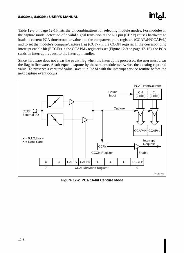
8x930Ax, 8x930Hx USER’S MANUAL
in
g
st clearpturedre the
Table 12-3 on page 12-15 lists the bit combinations for selecting module modes. For modulesthe capture mode, detection of a valid signal transition at the I/O pin (CEXx) causes hardware toload the current PCA timer/counter value into the compare/capture registers (CCAPxH/CCAPxL)and to set the module’s compare/capture flag (CCFx) in the CCON register. If the correspondininterrupt enable bit (ECCFx) in the CCAPMx register is set (Figure 12-9 on page 12-16), the PCAsends an interrupt request to the interrupt handler.
Since hardware does not clear the event flag when the interrupt is processed, the user muthe flag in firmware. A subsequent capture by the same module overwrites the existing cavalue. To preserve a captured value, save it in RAM with the interrupt service routine befonext capture event occurs.
Figure 12-2. PCA 16-bit Capture Mode
A4163-02
CCAPxH CCAPxL
CH (8 Bits)
CL (8 Bits)
CEXx External I/O
X O CAPPx CAPNx O O ECCFxO
CCFx
CCON Register
PCA Timer/Counter
Enable
Interrupt Request
Capture
07 CCAPMx Mode Register
x = 0,1,2,3 or 4 X = Don't Care
Count Input
12-6

PROGRAMMABLE COUNTER ARRAY
twaree, thee 16-
, the withpheral
fore
s
pt
er mustritten
12.3.2 Compare Modes
The compare function provides the capability for operating the five modules as timers, evencounters, or pulse width modulators. Four modes employ the compare function: 16-bit firmtimer mode, high-speed output mode, WDT mode, and PWM mode. In the first three of thescompare/capture module continuously compares the 16-bit PCA timer/counter value with thbit value pre-loaded into the module’s CCAPxH/CCAPxL register pair. In the PWM modemodule continuously compares the value in the low-byte PCA timer/counter register (CL)an 8-bit value in the CCAPxL module register. Comparisons are made three times per pericycle to match the fastest PCA timer/counter clocking rate (FOSC/4). For a description of periph-eral cycle timing, see “Clock and Reset Unit” on page 2-9.
Setting the ECOMx bit in a module’s mode register (CCAPMx) selects the compare functionthat module (Figure 12-9 on page 12-16). To use the modules in the compare modes, observe thfollowing general procedure:
1. Select the module’s mode of operation.
2. Select the input signal for the PCA timer/counter.
3. Load the comparison value into the module’s compare/capture register pair.
4. Set the PCA timer/counter run control bit.
5. After a match causes an interrupt, clear the module’s compare/capture flag.
12.3.3 16-bit Software Timer Mode
To program a compare/capture module for the 16-bit software timer mode (Figure 12-3), set theECOMx and MATx bits in the module’s CCAPMx register. Table 12-3 lists the bit combinationfor selecting module modes.
A match between the PCA timer/counter and the compare/capture registers (CCAPxH/CCAPxL)sets the module’s compare/capture flag (CCFx in the CCON register). This generates an interrurequest if the corresponding interrupt enable bit (ECCFx in the CCAPMx register) is set. Sincehardware does not clear the compare/capture flag when the interrupt is processed, the usclear the flag in firmware. During the interrupt routine, a new 16-bit compare value can be wto the compare/capture registers (CCAPxH/CCAPxL).
NOTETo prevent an invalid match while updating these registers, user firmware should write to CCAPxL first, then CCAPxH. A write to CCAPxL clears the ECOMx bit disabling the compare function, while a write to CCAPxH sets the ECOMx bit re-enabling the compare function.
12-7

8x930Ax, 8x930Hx USER’S MANUAL
firm-
nsaptureag
settingt
flag in
Figure 12-3. PCA Software Timer and Hi gh-speed Output Modes
12.3.4 High-speed Output Mode
The high-speed output mode (Figure 12-3) generates an output signal by toggling the module’sI/O pin (CEXx) when a match occurs. This provides greater accuracy than toggling pins in ware because the toggle occurs before the interrupt request is serviced. Thus, interrupt responsetime does not affect the accuracy of the output.
To program a compare/capture module for the high-speed output mode, set the ECOMx, MATx,TOGx bits in the module’s CCAPMx register. Table 12-3 on page 12-15 lists the bit combinatiofor selecting module modes. A match between the PCA timer/counter and the compare/cregisters (CCAPxH/CCAPxL) toggles the CEXx pin and sets the module’s compare/capture fl(CCFx in the CCON register). By setting or clearing the CEXx pin in firmware, the user selectswhether the match toggles the pin from low to high or vice versa.
The user also has the option of generating an interrupt request when the match occurs bythe corresponding interrupt enable bit (ECCFx in the CCAPMx register). Since hardware does noclear the compare/capture flag when the interrupt is processed, the user must clear thefirmware.
A4164-01
CCAPxH (8 Bits)
CCAPxL (8 Bits)
CH (8 Bits)
CL (8 Bits)
CEXx
X ECOMx 0 0 TOGx 0 ECCFxMATx
CCFx
PCA Timer/Counter
Enable
Interrupt Request
07 CCAPMx Mode Register
X = Don't Care x = 0, 1, 2, 3, 4 For software timer mode, set ECOMx and MATx. For high speed output mode, set ECOMx, MATx, and TOGx.
Compare/Capture Module
16-Bit Comparator
Count Input
ResetWrite to
CCAPxL
"0"
Match
"1"
Write to CCAPxH
Toggle
Enable
CCON
12-8

PROGRAMMABLE COUNTER ARRAY
t toggle value.pture
suc-d-off, elec-
cye reset
re/cap-e only
in the
ts inina-
y . Enter
enceo “ex-DT.
reset,
urs
urs,
ption.odules
If the user does not change the compare/capture registers in the interrupt routine, the nexoccurs after the PCA timer/counter rolls over and the count again matches the comparisonDuring the interrupt routine, a new 16-bit compare value can be written to the compare/caregisters (CCAPxH/CCAPxL).
NOTETo prevent an invalid match while updating these registers, user firmware should write to CCAPxL first, then CCAPxH. A write to CCAPxL clears the ECOMx bit disabling the compare function, while a write to CCAPxH sets the ECOMx bit re-enabling the compare function.
12.3.5 PCA Watchdog Timer Mode
A watchdog timer (WDT) provides the means to recover from routines that do not complete cessfully. A WDT automatically invokes a device reset if it does not regularly receive holsignals. WDTs are used in applications that are subject to electrical noise, power glitchestrostatic discharges, etc., or where high reliability is required.
In addition to the 8x930’s 14-bit hardware WDT, the PCA provides a programmable-frequen16-bit WDT as a mode option on compare/capture module 4. This mode generates a devicwhen the count in the PCA timer/counter matches the value stored in the module 4 compature registers. A PCA WDT reset has the same effect as an external reset. Module 4 is thPCA module that has the WDT mode. When not programmed as a WDT, it can be usedother modes.
To program module 4 for the PCA WDT mode (Figure 12-4), set the ECOM4 and MAT4 bithe CCAPM4 register and the WDTE bit in the CMOD register. Table 12-3 lists the bit combtions for selecting module modes. Also select the desired input for the PCA timer/counter bpro-gramming the CPS0 and CPS1 bits in the CMOD register (see Figure 12-7 on page 12-13)a 16-bit comparison value in the compare/capture registers (CCAP4H/CCAP4L). Enter a 16-bitinitial value in the PCA timer/counter (CH/CL) or use the reset value (0000H). The differbetween these values multiplied by the PCA input pulse rate determines the running time tpiration.” Set the timer/counter run control bit (CR in the CCON register) to start the PCA W
The PCA WDT generates a reset signal each time a match occurs. To hold off a PCA WDTthe user has three options:
• periodically change the comparison value in CCAP4H/CCAP4L so a match never occ
• periodically change the PCA timer/counter value so a match never occurs
• disable the module 4 reset output signal by clearing the WDTE bit before a match occthen later re-enable it
The first two options are more reliable because the WDT is not disabled as in the third oThe second option is not recommended if other PCA modules are in use, since the five mshare a common time base. Thus, in most applications the first option is the best one.
12-9

8x930Ax, 8x930Hx USER’S MANUAL
ion aslution to
ared
riod.
Figure 12-4. PCA Watchdog Timer Mode
12.3.6 Pulse Width Modulation Mode
The five PCA comparator/capture modules can be independently programmed to functpulse width modulators (Figure 12-5). The modulated output, which has a pulse width resoof eight bits, is available at the CEXx pin. The PWM output can be used to convert digital dataan analog signal with simple external circuitry.
In this mode the value in the low byte of the PCA timer/counter (CL) is continuously compwith the value in the low byte of the compare/capture register (CCAPxL). When CL < CCAPxL,the output waveform (Figure 12-6) is low. When a match occurs (CL = CCAPxL), the outputwaveform goes high and remains high until CL rolls over from FFH to 00H, ending the peAt roll over the output returns to a low, the value in CCAPxH is loaded into CCAPxL, and a newperiod begins.
A4165-01
CCAP4H (8 Bits)
CCAP4L (8 Bits)
CH (8 Bits)
CL (8 Bits)
X ECOM4 0 0 X 0 X1
WDTE
PCA Timer/Counter
PCA WDT Reset
07 CCAPM4 Mode Register
X = Don't Care
Compare/Capture Module
16-Bit Comparator
Count Input
ResetWrite to
CCAP4L
"0"
Match
"1"
Write to CCAP4H
EnableCMOD.6
12-10

PROGRAMMABLE COUNTER ARRAY
ignal
Figure 12-5. PCA 8-bit PWM Mode
The value in CCAPxL determines the duty cycle of the current period. The value in CCAPxH de-termines the duty cycle of the following period. Changing the value in CCAPxL over time mod-ulates the pulse width. As depicted in Figure 12-6, the 8-bit value in CCAPxL can vary from 0(100% duty cycle) to 255 (0.4% duty cycle).
NOTETo change the value in CCAPxL without glitches, write the new value to the high byte register (CCAPxH). This value is shifted by hardware into CCAPxL when CL rolls over from FFH to 00H.
The frequency of the PWM output equals the frequency of the PCA timer/counter input sdivided by 256. The highest frequency occurs when the FOSC/4 input is selected for the PCA tim-er/counter. For PLLSEL2:0 = 100 and FOSC = 12 MHz, this is 11.7 KHz. For PLLSEL2:0 = 110and FOSC = 12 MHz, this is 23.4 KHz.
A4166-01
CCAPxH
CEXx
X ECOMx 0 0 0 PWMx 00
07 CCAPMx Mode Register
X = Don't Care x = 0, 1, 2, 3, 4.
8-Bit Comparator
CL rollover from FFH to 00H loads CCAPxH contents into CCAPxL
"0"
"1"CL ≥ CCAPxL
CL < CCAPxL
CCAPxL
CL (8 Bits)
8
8
Enable
12-11

8x930Ax, 8x930Hx USER’S MANUAL
g the
e int (CR
To program a compare/capture module for the PWM mode, set the ECOMx and PWMx bits in themodule’s CCAPMx register. Table 12-3 on page 12-15 lists the bit combinations for selectingmodule modes. Also select the desired input for the PCA timer/counter by programminCPS0 and CPS1 bits in the CMOD register (see Figure 12-7). Enter an 8-bit value in CCAPxL tospecify the duty cycle of the first period of the PWM output waveform. Enter an 8-bit valuCCAPxH to specify the duty cycle of the second period. Set the timer/counter run control biin the CCON register) to start the PCA timer/counter.
Figure 12-6. PWM Variable Duty Cycle
A4161-01
Duty CycleCCAPxL
255
230
128
25
0
0.4%
10%
50%
90%
100%
1
0
1
0
1
0
1
0
Output Waveform
1
0
12-12

PROGRAMMABLE COUNTER ARRAY
CMOD Address: S:D9HReset State: 00XX X000B
PCA Timer/Counter Mode Register. Contains bits for selecting the PCA timer/counter input, disabling the PCA timer/counter during idle mode, enabling the PCA WDT reset output (module 4 only), and enabling the PCA timer/counter overflow interrupt.
7 0
CIDL WDTE — — — CPS1 CPS0 ECF
Bit Number
Bit Mnemonic Function
7 CIDL PCA Timer/Counter Idle Control:
CIDL = 1 disables the PCA timer/counter during idle mode. CIDL = 0 allows the PCA timer/counter to run during idle mode.
6 WDTE Watchdog Timer Enable:
WDTE = 1 enables the watchdog timer output on PCA module 4.WDTE = 0 disables the PCA watchdog timer output.
5:3 — Reserved:
Values read from these bits are indeterminate. Write zeros to these bits.
2:1 CPS1:0 PCA Timer/Counter Input Select:
CPS1 CPS0
0 0 FCLK /60 1 FCLK /21 0 Timer 0 overflow1 1 External clock at ECI pin (maximum rate = FOSC /8 )
0 ECF PCA Timer/Counter Interrupt Enable:
ECF = 1 enables the CF bit in the CCON register to generate an interrupt request.
Figure 12-7. CMOD: PCA Timer/Counter Mode Register
12-13

8x930Ax, 8x930Hx USER’S MANUAL
CCON Address: S:D8HReset State: 00X0 0000B
PCA Timer/Counter Control Register. Contains the run control bit and overflow flag for the PCA timer/counter, and the compare/capture flags for the five PCA compare/capture modules.
7 0
CF CR — CCF4 CCF3 CCF2 CCF1 CCF0
Bit Number
Bit Mnemonic Function
7 CF PCA Timer/Counter Overflow Flag:
Set by hardware when the PCA timer/counter rolls over. This generates an interrupt request if the ECF interrupt enable bit in CMOD is set. CF can be set by hardware or firmware but can be cleared only by firmware.
6 CR PCA Timer/Counter Run Control Bit:
Set and cleared by firmware to turn the PCA timer/counter on and off.
5 — Reserved:
The value read from this bit is indeterminate. Write a zero to this bit.
4:0 CCF4:0 PCA Module Compare/Capture Flags:
Set by hardware when a match or capture occurs. This generates a PCA interrupt request if the ECCFx interrupt enable bit in the corresponding CCAPMx register is set. Must be cleared by firmware.
Figure 12-8. CCON: PCA Timer/Counter Control Register
12-14

PROGRAMMABLE COUNTER ARRAY
Table 12-3. PCA Module Modes
ECOMx CAPPx CAPNx MATx TOGx PWMx ECCFx Module Mode
0 0 0 0 0 0 0 No operation
X 1 0 0 0 0 X 16-bit capture on positive-edge trigger at CEXx
X 0 1 0 0 0 X 16-bit capture on negative-edge trigger at CEXx
X 1 1 0 0 0 X 16-bit capture on positive- or negative-edge trigger at CEXx
1 0 0 1 0 0 X Compare: firmware timer
1 0 0 1 1 0 X Compare: high-speed output
1 0 0 0 0 1 0 Compare: 8-bit PWM
1 0 0 1 X 0 X Compare: PCA WDT (CCAPM4 only) (Note 3)
NOTES:1. This table shows the CCAPMx register bit combinations for selecting the operating modes of the PCA
compare/capture modules. Other bit combinations are invalid. See Figure 12-9 for bit definitions.2. x = 0–4, X = Don’t care.3. For PCA WDT mode, also set the WDTE bit in the CMOD register to enable the reset output signal.
12-15

8x930Ax, 8x930Hx USER’S MANUAL
CCAPMx (x = 0–4) Address: CCAPM0 S:DAHCCAPM1 S:DBHCCAPM2 S:DCHCCAPM3 S:DDHCCAPM4 S:DEH
Reset State: x000 0000B
PCA Module Compare/Capture Registers. These five register pairs store the 16-bit comparison value or captured value for the corresponding compare/capture modules. In the PWM mode, the low-byte register controls the duty cycle of the output waveform.
7 0
— ECOMx CAPPx CAPNx MATx TOGx PWMx ECCFx
Bit Number
Bit Mnemonic Function
7 — Reserved:
The value read from this bit is indeterminate. Write a zero to this bit.
6 ECOMx Compare Modes:
ECOMx = 1 enables the module comparator function. The comparator is used to implement the firmware timer, high-speed output, pulse width modulation, and watchdog timer modes.
5 CAPPx Capture Mode (Positive):
CAPPx = 1 enables the capture function with capture triggered by a positive edge on pin CEXx.
4 CAPNx Capture Mode (Negative):
CAPNx = 1 enables the capture function with capture triggered by a negative edge on pin CEXx.
3 MATx Match:
Set ECOMx and MATx to implement the firmware timer mode. When MATx = 1, a match of the PCA timer/counter with the compare/capture register sets the CCFx bit in the CCON register, flagging an interrupt.
2 TOGx Toggle:
Set ECOMx, MATx, and TOGx to implement the high-speed output mode. When TOGx = 1, a match of the PCA timer/counter with the compare/capture register toggles the CEXx pin.
1 PWMx Pulse Width Modulation Mode:
PWMx = 1 configures the module for operation as an 8-bit pulse width modulator with output waveform on the CEXx pin.
0 ECCFx Enable CCFx Interrupt:
Enables compare/capture flag CCFx in the CCON register to generate an interrupt request.
Figure 12-9. CCAPM x: PCA Compare/Capture Module Mode Registers
12-16

13Serial I/O Port

heralthe se-
t oper-des and at
o er 1 and
ers are
e RXD
lds re-rs. Togister
ll over-tively.
rt.
CHAPTER 13SERIAL I/O PORT
The serial input/output port supports communication with modems and other external peripdevices. This chapter provides instructions for programming the serial port and generating rial I/O baud rates with timer 1 and timer 2.
13.1 OVERVIEW
The serial I/O port provides both synchronous and asynchronous communication modes. Iates as a universal asynchronous receiver and transmitter (UART) in three full-duplex mo(modes 1, 2, and 3). Asynchronous transmission and reception can occur simultaneouslydifferent baud rates. The UART supports framing-bit error detection, multiprocessor communi-cation, and automatic address recognition. The serial port also operates in a single synchronousmode (mode 0).
The synchronous mode (mode 0) operates at a single baud rate. Mode 2 operates at twbaudrates. Modes 1 and 3 operate over a wide range of baud rates, which are generated by timtimer 2. Baud rates are detailed in “Baud Rates” on page 13-10.
NOTEThe baud rate calculations in this chapter are based on the value of FCLK which is a function of PLLSEL2:0. See Table 2-4 and Figure 2-6 on page 2-9.
The serial port signals are defined in Table 13-1, and the serial port special function registdescribed in Table 13-2. Figure 13-1 is a block diagram of the serial port.
For the three asynchronous modes, the UART transmits on the TXD pin and receives on thpin. For the synchronous mode (mode 0), the UART outputs a clock signal on the TXD pin andsends and receives messages on the RXD pin (Figure 13-1). The SBUF register, which hoceived bytes and bytes to be transmitted, actually consists of two physically different registesend, firmware writes a byte to SBUF; to receive, firmware reads SBUF. The receive shift reallows reception of a second byte before the first byte has been read from SBUF. However, if firm-ware has not read the first byte by the time the second byte is received, the second byte wiwrite the first. The UART sets interrupt bits TI and RI on transmission and reception, respecThese two bits share a single interrupt request and interrupt vector.
The serial port control (SCON) register (Figure 13-2) configures and controls the serial po
13-1

8x930Ax, 8x930Hx USER’S MANUAL
pabil- puls-its are2) of
on.
6P2 ofycle,e. Inf the
13.2 MODES OF OPERATION
The serial I/O port can operate in one synchronous and three asynchronous modes.
13.2.1 Synchronous Mode (Mode 0)
Mode 0 is a half-duplex, synchronous mode, which is commonly used to expand the I/O caities of a device with shift registers. The transmit data (TXD) pin outputs a set of eight clockes while the receive data (RXD) pin transmits or receives a byte of data. The eight data btransmitted and received least-significant bit (LSb) first. Shifts occur in the last phase (S6Pevery peripheral cycle, which corresponds to a baud rate of FCLK/6. Figure 13-3 on page 13-6shows the timing for transmission and reception in mode 0.
13.2.1.1 Transmission ( Mode 0)
Follow these steps to begin a transmission:
1. Write to the SCON register, clearing bits SM0, SM1, and REN.
2. Write the byte to be transmitted to the SBUF register. This write starts the transmissi
Hardware executes the write to SBUF in the last phase (S6P2) of a peripheral cycle. At Sthe following cycle, hardware shifts the LSb (D0) onto the RXD pin. At S3P1 of the next cthe TXD pin goes low for the first clock-signal pulse. Shifts continue every peripheral cyclthe ninth cycle after the write to SBUF, the MSB (D7) is on the RXD pin. At the beginning o
Table 13-1. Serial Port Signals
FunctionName Type Description Multiplexed
With
TXD O Transmit Data. In mode 0, TXD transmits the clock signal. In modes 1, 2, and 3, TXD transmits serial data.
P3.1
RXD I/O Receive Data. In mode 0, RXD transmits and receives serial data. In modes 1, 2, and 3, RXD receives serial data.
P3.0
Table 13-2. Serial Port Special Function Registers
Mnemonic Description Address
SBUF Serial Buffer . Two separate registers, accessed with same address comprise the SBUF register. Writing to SBUF loads the transmit buffer; reading SBUF accesses the receive buffer.
S:99H
SCON Serial Port Control . Selects the serial port operating mode. SCON enables and disables the receiver, framing bit error detection, multiprocessor communication, automatic address recognition, and the serial port interrupt bits.
S:98H
SADDR Serial Address . Defines the individual address for a slave device. S:A8H
SADEN Serial Address Enable. Specifies the mask byte that is used to define the given address for a slave device.
S:B8H
13-2

SERIAL I/O PORT
of the
nd set
firstift- shift-eption.
tenth cycle, hardware drives the RXD pin high and asserts TI (S1P1) to indicate the endtransmission.
13.2.1.2 Reception ( Mode 0)
To start a reception in mode 0, write to the SCON register. Clear bits SM0, SM1, and RI athe REN bit.
Hardware executes the write to SCON in the last phase (S6P2) of a peripheral cycle (Figure 13-3).In the second peripheral cycle following the write to SCON, TXD goes low at S3P1 for theclock-signal pulse, and the LSb (D0) is sampled on the RXD pin at S5P2. The D0 bit is then shed into the shift register. After eight shifts at S6P2 of every peripheral cycle, the LSb (D7) ised into the shift register, and hardware asserts RI (S1P1) to indicate a completed recFirmware can then read the received byte from SBUF.
Figure 13-1. Serial Port Block Diagram
A4123-01
SBUF (Receive)
Receive Shift Register
SBUF (Transmit)
Read SBUFWrite SBUF
Mode 0 Transmit
TxD
RxD
SCON
TIRI
Interrupt Request
Serial I/O Control
IB Bus
Load SBUF
13-3

8x930Ax, 8x930Hx USER’S MANUAL
SCON Address: S:98HReset State: 0000 0000B
Serial Port Control Register. SCON contains serial I/O control and status bits, including the mode select bits and the interrupt flag bits.
7 0
FE/SM0 SM1 SM2 REN TB8 RB8 TI RI
Bit Number
Bit Mnemonic Function
7 FE
SM0
Framing Error Bit:
To select this function, set the SMOD0 bit in the PCON register. Set by hardware to indicate an invalid stop bit. Cleared by firmware, not by valid frames.
Serial Port Mode Bit 0:
To select this function, clear the SMOD0 bit in the PCON register. Firmware writes to bits SM0 and SM1 to select the serial port operating mode. Refer to the SM1 bit for the mode selections.
6 SM1 Serial Port Mode Bit 1:
Firmware writes to bits SM1 and SM0 (above) to select the serial port operating mode.
SM0 SM1 Mode Description Baud Rat e†
0 0 0 Shift register FCLK/60 1 1 8-bit UART Variable1 0 2 9-bit UART FCLK/16†† or FCLK/32††
1 1 3 9-bit UART Variable†The baud rate calculations in this chapter are based on the value of FCLK which is a function of PLLSEL2:0. See Table 2-4 and Figure 2-6 on page 2-9.††Select by programming the SMOD bit in the PCON register (see section “Baud Rates” on page 13-10).
5 SM2 Serial Port Mode Bit 2:
Firmware writes to bit SM2 to enable and disable the multiprocessor communication and automatic address recognition features. This allows the serial port to differentiate between data and command frames and to recognize slave and broadcast addresses.
4 REN Receiver Enable Bit:
To enable reception, set this bit. To enable transmission, clear this bit.
3 TB8 Transmit Bit 8:
In modes 2 and 3, firmware writes the ninth data bit to be transmitted to TB8. Not used in modes 0 and 1.
Figure 13-2. SCON: Serial Port Control Register
13-4

SERIAL I/O PORT
2 RB8 Receiver Bit 8:
Mode 0: Not used.
Mode 1 (SM2 clear): Set or cleared by hardware to reflect the stop bit received.
Modes 2 and 3 (SM2 set): Set or cleared by hardware to reflect the ninth data bit received.
1 TI Transmit Interrupt Flag Bit:
Set by the transmitter after the last data bit is transmitted. Cleared by firmware.
0 RI Receive Interrupt Flag Bit:
Set by the receiver after the last data bit of a frame has been received. Cleared by firmware.
SCON (Continued) Address: S:98HReset State: 0000 0000B
Serial Port Control Register. SCON contains serial I/O control and status bits, including the mode select bits and the interrupt flag bits.
7 0
FE/SM0 SM1 SM2 REN TB8 RB8 TI RI
Bit Number
Bit Mnemonic Function
Figure 13-2. SCON: Serial Port Control Register (Continued)
13-5

8x930Ax, 8x930Hx USER’S MANUAL
Figure 13-3. Mode 0 Timing
Figure 13-4. Data Frame (Modes 1, 2, and 3)
A4124-02
TXD
RXD D1
ShiftS6P2 S6P2 S6P2 S6P2
Write to SBUF
S3P1 S6P1
D2D0 D6 D7
S6P2S6P2
Transmit
TI
TXD
S3P1 S6P1Write to SCON
RI
ShiftS6P2 S6P2 S6P2 S6P2
RXD
S1P1Receive
Set REN, Clear RI
D0 D1 D6 D7
S6P2
S5P2S6P2
S1P1
S6P2
S6P2
D0 D7 D8D1 D2 D3 D4 D5 D6
Stop Bit
Ninth Data Bit (Modes 2 and 3 only)Start Bit
Data Byte
A2261-01
13-6

SERIAL I/O PORT
itted it is er 1
LSb e it in
he
on.
ini-
aming pagelid stopssionister
t, onlycannot
13.2.2 Asynchronous Modes (Modes 1, 2, and 3)
The serial port has three asynchronous modes of operation:
• Mode 1. Mode 1 is a full-duplex, asynchronous mode. The data frame (Figure 13-4) consists of 10 bits: one start bit, eight data bits, and one stop bit. Serial data is transmon the TXD pin and received on the RXD pin. When a message is received, the stop bread in the RB8 bit in the SCON register. The baud rate is generated by overflow of timor timer 2 (see “Baud Rates” on page 13-10).
• Modes 2 and 3. Modes 2 and 3 are full-duplex, asynchronous modes. The data frame (Figure 13-4) consists of 11 bits: one start bit, eight data bits (transmitted and receivedfirst), one programmable ninth data bit, and one stop bit. Serial data is transmitted on thTXD pin and received on the RXD pin. On receive, the ninth bit is read from the RB8 bthe SCON register. On transmit, the ninth data bit is written to the TB8 bit in the SCONregister. Alternatively, you can use the ninth bit as a command/data flag.
— In mode 2, the baud rate is programmable to 1/16 or 1/32 internal frequency, FCLK.
— In mode 3, the baud rate is generated by overflow of timer 1 or timer 2.
13.2.2.1 Transmission ( Modes 1, 2, 3)
Follow these steps to initiate a transmission:
1. Write to the SCON register. Select the mode with the SM0 and SM1 bits, and clear tREN bit. For modes 2 and 3, also write the ninth bit to the TB8 bit.
2. Write the byte to be transmitted to the SBUF register. This write starts the transmissi
13.2.2.2 Reception ( Modes 1, 2, 3)
To prepare for a reception, set the REN bit in the SCON register. The actual reception is then tiated by a detected high-to-low transition on the RXD pin.
13.3 FRAMING BIT ERROR DETECTION (MODES 1, 2, AND 3)
Framing bit error detection is provided for the three asynchronous modes. To enable the frbit error detection feature, set the SMOD0 bit in the PCON register (see Figure 15-1 on15-3). When this feature is enabled, the receiver checks each incoming data frame for a vabit. An invalid stop bit may result from noise on the serial lines or from simultaneous transmiby two CPUs. If a valid stop bit is not found, the firmware sets the FE bit in the SCON reg(see Figure 13-2).
Firmware may examine the FE bit after each reception to check for data errors. Once sefirmware or a reset can clear the FE bit. Subsequently received frames with valid stop bits clear the FE bit.
13-7

8x930Ax, 8x930Hx USER’S MANUAL
nableessor
inth bit slave
ith the If thed the RI
s to re-e waiting
ication
muni-mandit in the
mand
nfigu-eivedit.
13.4 MULTIPROCESSOR COMMUNICATION (MODES 2 AND 3)
Modes 2 and 3 provide a ninth-bit mode to facilitate multiprocessor communication. To ethis feature, set the SM2 bit in the SCON register (see Figure 13-2). When the multiproccommunication feature is enabled, the serial port can differentiate between data frames (nclear) and address frames (ninth bit set). This allows the microcontroller to function as aprocessor in an environment where multiple slave processors share a single serial line.
When the multiprocessor communication feature is enabled, the receiver ignores frames wninth bit clear. The receiver examines frames with the ninth bit set for an address match.received address matches the slave’s address, the receiver hardware sets the RB8 bit anbit in the SCON register, generating an interrupt.
NOTEThe ES bit must be set in the IEN0 register to allow the RI bit to generate an interrupt. The IEN0 register is described in Chapter 8, Interrupts.
The addressed slave’s firmware then clears the SM2 bit in the SCON register and prepareceive the data bytes. The other slaves are unaffected by these data bytes because they arto respond to their own addresses.
13.5 AUTOMATIC ADDRESS RECOGNITION
The automatic address recognition feature is enabled when the multiprocessor communfeature is enabled (i.e., the SM2 bit is set in the SCON register).
Implemented in hardware, automatic address recognition enhances the multiprocessor comcation feature by allowing the serial port to examine the address of each incoming comframe. Only when the serial port recognizes its own address does the receiver set the RI bSCON register to generate an interrupt. This ensures that the CPU is not interrupted by comframes addressed to other devices.
If desired, you may enable the automatic address recognition feature in mode 1. In this coration, the stop bit takes the place of the ninth data bit. The RI bit is set only when the reccommand frame address matches the device’s address and is terminated by a valid stop b
NOTEThe multiprocessor communication and automatic address recognition features cannot be enabled in mode 0 (i.e., setting the SM2 bit in the SCON register in mode 0 has no effect).
To support automatic address recognition, a device is identified by a given address and a broad-cast address.
13-8

SERIAL I/O PORT
e. To
bit 0 only,
t (e.g.,
esit 2 set
t, bit 1
with
st
13.5.1 Given Address
Each device has an individual address that is specified in the SADDR register; the SADEN reg-ister is a mask byte that contains don't-care bits (defined by zeros) to form the device’s given ad-dress. These don't-care bits provide the flexibility to address one or more slaves at a timaddress a device by its individual address, the SADEN mask byte must be 1111 1111 The follow-ing example illustrates how a given address is formed:
The following is an example of how to use given addresses to address different slaves:
The SADEN byte is selected so that each slave may be addressed separately. For Slave A, (the LSb) is a don't-care bit; for Slaves B and C, bit 0 is a 1. To communicate with Slave Athe master must send an address where bit 0 is clear (e.g., 1111 0000).
For Slave A, bit 1 is a 0; for Slaves B and C, bit 1 is a don’t-care bit. To communicate with SlavesB and C, but not Slave A, the master must send an address with bits 0 and 1 both se1111 0011).
For Slaves A and B, bit 2 is a don’t-care bit; for Slave C, bit 2 is a 0. To communicate with SlavA and B, but not Slave C, the master must send an address with bit 0 set, bit 1 clear, and b(e.g., 1111 0101).
To communicate with Slaves A, B, and C, the master must send an address with bit 0 seclear, and bit 2 clear (e.g., 1111 0001).
13.5.2 Broadcast Address
A broadcast address is formed from the logical OR of the SADDR and SADEN registers zeros defined as don't-care bits, e.g.:
The use of don't-care bits provides flexibility in defining the broadcast address, however, in moapplications, a broadcast address is 0FFH.
SADDR
SADEN
Given
=
=
=
0101 0110
1111 1100
0101 01XX
Slave A: SADDR
SADEN
Given
=
=
=
1111 0001
1111 1010
1111 0X0X
Slave C: SADDR
SADEN
Given
=
=
=
1111 0010
1111 1101
1111 00X1
Slave B: SADDR
SADEN
Given
=
=
=
1111 0011
1111 1001
1111 0XX1
SADDR
SADEN
(SADDR) OR (SADEN)
=
=
=
0101 0110
1111 1100
1111 111X
13-9

8x930Ax, 8x930Hx USER’S MANUAL
all of
BH.
stom-
modesort caneptiond for the
The following is an example of using broadcast addresses:
For Slaves A and B, bit 2 is a don’t-care bit; for Slave C, bit 2 is set. To communicate with the slaves, the master must send an address FFH.
To communicate with Slaves A and B, but not Slave C, the master can send an address F
13.5.3 Reset Addresses
On reset, the SADDR and SADEN registers are initialized to 00H, that is, the given and broadcaaddresses are xxxx xxxx (all don't-care bits). This ensures that the serial port is backwards-cpatible with MCS® 51 microcontrollers that do not support automatic address recognition.
13.6 BAUD RATES
You must select the baud rate for the serial port transmitter and receiver when operating in 1, 2, and 3. (The baud rate is preset for mode 0.) In its asynchronous modes, the serial ptransmit and receive simultaneously. Depending on the mode, the transmission and recrates can be the same or different. Table 13-3 summarizes the baud rates that can be usefour serial I/O modes.
NOTEThe baud rate calculations in this chapter are based on the value of FCLK which is a function of PLLSEL2:0. See Table 2-4 and Figure 2-6 on page 2-9.
13.6.1 Baud Rate for Mode 0
The baud rate for mode 0 is fixed at FCLK/6.
Slave A: SADDR
SADEN
Broadcast
=
=
=
1111 0001
1111 1010
1111 1X11
Slave C: SADDR
SADEN
Broadcast
=
=
=
1111 0010
1111 1101
1111 1111
Slave B: SADDR
SADEN
Broadcast
=
=
=
1111 0011
1111 1001
1111 1X11
Table 13-3. Summary of Baud Rates
Mode No. of Baud Rates
Send and Receiveat the Same Rate
Send and Receiveat Different Rates
0 1 N/A N/A
1 Many †† Yes Yes
2 2 Yes No
3 Many †† Yes Yes
†† Baud rates are determined by overflow of timer 1 and/or timer 2.
13-10
SERIAL I/O PORT
2. You receiv-
and 3. in the
age
OD
.
13.6.2 Baud Rates for Mode 2
Mode 2 has two baud rates, which are selected by the SMOD1 bit in the PCON register (Figure15-1 on page 15-3). The following expression defines the baud rate:
13.6.3 Baud Rates for Modes 1 and 3
In modes 1 and 3, the baud rate is generated by overflow of timer 1 (default) and/or timer may select either or both timer(s) to generate the baud rate(s) for the transmitter and/or theer.
13.6.3.1 Timer 1 Generated Baud Rates (Modes 1 and 3)
Timer 1 is the default baud rate generator for the transmitter and the receiver in modes 1The baud rate is determined by the timer 1 overflow rate and the value of SMOD, as shownfollowing formula:
13.6.3.2 Selecting Timer 1 as the Baud Rate Generator
To select timer 1 as the baud rate generator:
• Disable the timer interrupt by clearing the ET1 bit in the IEN0 register (Figure 6-12 on p6-25).
• Configure timer 1 as a timer or an event counter (set or clear the C/T# bit in the TMODregister, Figure 11-5 on page 11-7).
• Select timer mode 0–3 by programming the M1 and M0 bits in the TMOD register.
In most applications, timer 1 is configured as a timer in auto-reload mode (high nibble of TM= 0010B). The resulting baud rate is defined by the following expression:
Timer 1 can generate very low baud rates with the following setup:
• Enable the timer 1 interrupt by setting the ET1 bit in the IEN0 register.
• Configure timer 1 to run as a 16-bit timer (high nibble of TMOD = 0001B).
• Use the timer 1 interrupt to initiate a 16-bit firmware reload.
Table 13-4 lists commonly used baud rates and shows how they are generated by timer 1
Serial I/O Mode 2 Baud Rate 2SMOD1 FCLK
32-----------×=
Serial I/O Modes 1 and 3 Baud Rate 2SMOD1 Timer 1 Overflow Rate32
------------------------------------------------------------×=
Serial I/O Modes 1 and 3 Baud Rate 2SMOD1 FCLK
16 12 256 TH1 )(–[ ]××------------------------------------------------------------------×=
13-11

8x930Ax, 8x930Hx USER’S MANUAL
(Figure in the and
m theiffer-to itsnot setXF2L2).ON.
timer
13.6.3.3 Timer 2 Generated Baud Rates (Modes 1 and 3)
Timer 2 may be selected as the baud rate generator for the transmitter and/or receiver 13-5). The timer 2 baud rate generator mode is similar to the auto-reload mode. A rolloverTH2 register reloads registers TH2 and TL2 with the 16-bit value in registers RCAP2HRCAP2L, which are preset by firmware.
The timer 2 baud rate is expressed by the following formula:
13.6.3.4 Selecting Timer 2 as the Baud Rate Generator
To select timer 2 as the baud rate generator for the transmitter and/or receiver, prograRCLCK and TCLCK bits in the T2CON register as shown in Table 13-5. (You may select dent baud rates for the transmitter and receiver.) Setting RCLK and/or TCLK puts timer 2 inbaud rate generator mode (Figure 13-5). In this mode, a rollover in the TH2 register does the TF2 bit in the T2CON register. Also, a high-to-low transition at the T2EX pin sets the Ebit in the T2CON register but does not cause a reload from (RCAP2H, RCAP2L) to (TH2, TYou can use the T2EX pin as an additional external interrupt by setting the EXEN2 bit in T2C
NOTETurn the timer off (clear the TR2 bit in the T2CON register) before accessing registers TH2, TL2, RCAP2H, and RCAP2L.
You may configure timer 2 as a timer or a counter. In most applications, it is configured for operation (i.e., the C/T2# bit is clear in the T2CON register).
Table 13-4. Timer 1 Generated Baud Rates for Serial I/O Modes 1 and 3
Baud Rate
Oscillator Frequency
(FCLK)SMOD1
Timer 1
C/T# Mode Reload Value
125.0 Kbaud (max) † 12.0 MHz 1 0 2 FFH
62.5 Kbaud † 6.0 MHz 1 0 2 FFH
110.0 Baud 3.0 MHz 0 0 2 72H
110.0 Baud † 6.0 MHz 0 0 1 FEEBH
† The baud rate calculations in this chapter are based on the value of FCLK which is a function of PLLSEL2:0. See Table 2-4 and Figure 2-6 on page 2-9.
Serial I/O Modes 1 and 3 Baud Rate Timer 2 Overflow Rate
16------------------------------------------------------------=
13-12
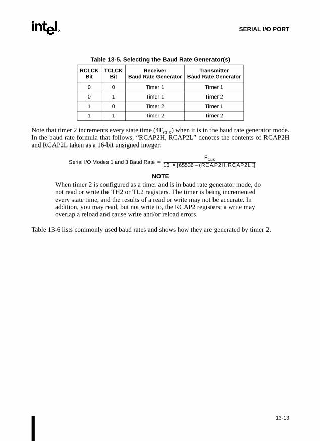
SERIAL I/O PORT
e.
.
Note that timer 2 increments every state time (4FCLK) when it is in the baud rate generator modIn the baud rate formula that follows, “RCAP2H, RCAP2L” denotes the contents of RCAP2Hand RCAP2L taken as a 16-bit unsigned integer:
NOTEWhen timer 2 is configured as a timer and is in baud rate generator mode, do not read or write the TH2 or TL2 registers. The timer is being incremented every state time, and the results of a read or write may not be accurate. In addition, you may read, but not write to, the RCAP2 registers; a write may overlap a reload and cause write and/or reload errors.
Table 13-6 lists commonly used baud rates and shows how they are generated by timer 2
Table 13-5. Selecting the Baud Rate Generator(s)
RCLCKBit
TCLCKBit
Receiver Baud Rate Generator
Transmitter Baud Rate Generator
0 0 Timer 1 Timer 1
0 1 Timer 1 Timer 2
1 0 Timer 2 Timer 1
1 1 Timer 2 Timer 2
Serial I/O Modes 1 and 3 Baud Rate FCLK
16 65536 RCAP2H RCAP2L ),(–[ ]×-------------------------------------------------------------------------------------------------------=
13-13

8x930Ax, 8x930Hx USER’S MANUAL
Figure 13-5. Timer 2 in Baud Rate Generator Mode
Table 13-6. Timer 2 Generated Baud Rates
Baud RateInternal
Frequency(FCLK)
RCAP2H RCAP2L
750.0 Kbaud †† 12 MHz FF FF
375.0 Kbaud †† 6 MHz FFH FFH
9.6 Kbaud †† 6 MHz FFH D9H
4.8 Kbaud †† 6 MHz FFH B2H
2.4 Kbaud †† 6 MHz FFH 64H
1.2 Kbaud †† 6 MHz FEH C8H
300.0 baud †† 6 MHz FBH 1EH
110.0 baud †† 6 MHz F2H AFH
300.0 baud 3 MHz FDH 8FH
110.0 baud 3 MHz F9H 57H
†† See note on page page 13-1.
T2EX
T2
Timer 1 Overflow
TR2
TH2 (8 Bits)
TL2 (8 Bits)
EXEN2
EXF2
A5205-01
FCLK
RCAP2H RCAP2L
C/T2#
0
1
Interrupt Request
0
1
SMOD1
1
0
RCLCK
16
1
0
TCLCK
RX Clock
TX Clock
2
16
Note availability of additional external interrupt.
13-14

14Minimum Hardware Setup

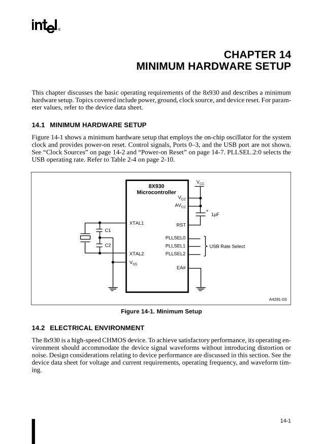
ystem
cts the
ng en-on orSee them tim-
CHAPTER 14MINIMUM HARDWARE SETUP
This chapter discusses the basic operating requirements of the 8x930 and describes a minimumhardware setup. Topics covered include power, ground, clock source, and device reset. For param-eter values, refer to the device data sheet.
14.1 MINIMUM HARDWARE SETUP
Figure 14-1 shows a minimum hardware setup that employs the on-chip oscillator for the sclock and provides power-on reset. Control signals, Ports 0–3, and the USB port are not shown.See “Clock Sources” on page 14-2 and “Power-on Reset” on page 14-7. PLLSEL.2:0 seleUSB operating rate. Refer to Table 2-4 on page 2-10.
Figure 14-1. Minimum Setup
14.2 ELECTRICAL ENVIRONMENT
The 8x930 is a high-speed CHMOS device. To achieve satisfactory performance, its operativironment should accommodate the device signal waveforms without introducing distortinoise. Design considerations relating to device performance are discussed in this section. device data sheet for voltage and current requirements, operating frequency, and waveforing.
8X930 Microcontroller
A4291-03
XTAL2
VSS
VCC
VCC
XTAL1 RSTC1
C2
1µF+
AVCC
EA#
USB Rate Select
PLLSEL0
PLLSEL1
PLLSEL2
14-1

8x930Ax, 8x930Hx USER’S MANUAL
Use
inter-
power
noise
or
amic or the0.
fre- as antor de-rasitic
ith high
and
PDn.
be-e chip of
14.2.1 Power and Ground Pins
Power the 8x930 from a well-regulated power supply designed for high-speed digital loads.short, low impedance connections to the power (VCC) and ground (VSS) pins.
14.2.2 Unused Pins
To provide stable, predictable performance, connect unused input pins to VSS or VCC. Untermi-nated input pins can float to a mid-voltage level and draw excessive current. Unterminatedrupt inputs may generate spurious interrupts.
14.2.3 Noise Considerations
The fast rise and fall times of high-speed CHMOS logic may produce noise spikes on the supply lines and signal outputs. To minimize noise and waveform distortion, follow good boardlayout techniques. Use sufficient decoupling capacitors and transient absorbers to keepwithin acceptable limits. Connect 0.01 µF bypass capacitors between VCC and each VSS pin. Placethe capacitors close to the device to minimize path lengths.
Multi-layer printed circuit boards with separate VCC and ground planes help minimize noise. Fadditional information on noise reduction, see Application Note AP-125, “Designing Microcon-troller Systems for Electrically Noisy Environments.”
14.3 CLOCK SOURCES
The 8x930 can use an external clock (Figure 14-3), an on-chip oscillator with crystal or cerresonator (Figure 14-2), or an on-chip phase-locked oscillator (locked to the external clockon-chip oscillator) as its clock source. For USB operating rates, see Table 2-4 on page 2-1
14.3.1 On-chip Oscillator (Crystal)
This clock source uses an external quartz crystal connected from XTAL1 to XTAL2 as thequency-determining element (Figure 14-2). The crystal operates in its fundamental modeinductive reactance in parallel resonance with capacitance external to the crystal. Oscillasign considerations include crystal specifications, operating temperature range, and paboard capacitance. Consult the crystal manufacturer’s data sheet for parameter values. Wquality components, C1 = C2 = 30 pF is adequate for this application.
Pins XTAL1 and XTAL2 are protected by on-chip electrostatic discharge (ESD) devices, D1D2, which are diodes parasitic to the RF FETs. They serve as clamps to VCC and VSS. Feedbackresistor RF in the inverter circuit, formed from paralleled n- and p- channel FETs, permits thebit in the PCON register (Figure 15-1 on page 15-3) to disable the clock during powerdow
Noise spikes at XTAL1 and XTAL2 can disrupt microcontroller timing. To minimize coupling tween other digital circuits and the oscillator, locate the crystal and the capacitors near thand connect to XTAL1, XTAL2, and VSS with short, direct traces. To further reduce the effectsnoise, place guard rings around the oscillator circuitry and ground the metal crystal case.
14-2

MINIMUM HARDWARE SETUP
tion ofded
eramiction.
ownte. If
xternal
wer ise (i.e.,mains
For a more in-depth discussion of crystal specifications, ceramic resonators, and the selecC1 and C2 see Applications Note AP-155, “Oscillators for Microcontrollers,” in the EmbedApplications handbook.
14.3.2 On-chip Oscillator (Ceramic Resonator)
In cost-sensitive applications, you may choose a ceramic resonator instead of a crystal. Cresonator applications may require slightly different capacitor values and circuit configuraConsult the manufacturer’s data sheet for specific information.
Figure 14-2. CHMOS On-chip Oscillator
14.3.3 External Clock
To operate the 8x930 from an external clock, connect the clock source to the XTAL1 pin as shin Figure 14-3. Leave the XTAL2 pin floating. The external clock driver can be a CMOS gathe clock driver is a TTL device, its output must be connected to VCC through a 4.7 kΩ pullupresistor.
For external clock drive requirements, see the device data sheet. Figure 14-4 shows the clock drivewaveform. The external clock source must meet the minimum high and low times (TCHCX andTCLCX) and the maximum rise and fall times (TCLCH and TCHCL) to minimize the effect of externalnoise on the clock generator circuit. Long rise and fall times increase the chance that enoise will affect the clock circuitry and cause unreliable operation.
The external clock driver may encounter increased capacitance loading at XTAL1 when poapplied, due to the interaction between the internal amplifier and its feedback capacitancthe Miller effect). Once the input waveform requirements are met, the input capacitance reunder 20 pF.
A4143-03
XTAL2
XTAL1
C1
C2
VCC
PD#
To Internal Timing Circuit
Inte
rnal
RF
Quartz Crystal or Ceramic Resonator D1
D2
Ext
erna
l
14-3

8x930Ax, 8x930Hx USER’S MANUAL
Figure 14-3. External Clock Connection for the 8 x930
Figure 14-4. External Clock Drive Waveforms
XTAL2
VSS
XTAL1
N/C
External Clock
CMOS Clock Driver
A4142-03
Note: If TTL clock driver is used, connect a 4.7kΩ pullup resistor from driver output to VCC.
0.7 VCC
A4119-01
0.45 V
VCC – 0.5
0.2 VCC – 0.1
TCHCL
TCLCX
TCLCL
TCLCH TCHCX
14-4

MINIMUM HARDWARE SETUP
eansould
eet)
a cold
when
exam-ower-
by ca-ST
tes ag Tim-
14.4 RESET
A device reset initializes the 8x930 and vectors the CPU to address FF:0000H. A reset is a mof exiting the idle and powerdown modes or recovering from firmware malfunctions, and cbe a USB reset initiated by the host or upstream hub.
NOTEA reset is required after applying power.
To achieve a valid reset, VCC must be within its normal operating range (see device data shand the reset signal must be maintained for 64 clock cycles (64TOSC) after the oscillator has sta-bilized.
Device reset is initiated in three ways:
• externally, by asserting the RST pin
• internally, if the hardware WDT or the PCA WDT expires
• over the bus, by a USB-initiated reset
These three reset mechanisms are ORed to create a single reset signal for the 8x930.
The power off flag (POF) in the PCON register indicates whether a reset is a warm start orstart. A cold start reset (POF = 1) is a reset that occurs after power has been off or VCC has fallenbelow 3 V, so the contents of volatile memory are indeterminate. POF is set by hardwareVCC rises from less than 3 V to its normal operating level. See “Power Off Flag” on page 15-2. Awarm start reset (POF = 0) is a reset that occurs while the chip is at operating voltage, for ple, a reset initiated by a WDT overflow or an external reset used to terminate the idle or pdown modes.
14.4.1 Externally-Initiated Resets
To reset the 8x930, hold the RST pin at a logic high for at least 64 clock cycles (64TOSC) while theoscillator is running. Reset can be accomplished automatically at the time power is appliedpacitively coupling RST to VCC (see Figure 14-1 and “Power-on Reset” on page 14-7). The Rpin has a Schmitt trigger input and a pulldown resistor.
14.4.2 WDT-initiated Resets
Expiration of the hardware WDT (overflow) or the PCA WDT (comparison match) generareset signal. WDT initiated resets have the same effect as an external reset. See “Watchdoer” on page 11-16 and section “PCA Watchdog Timer Mode” on page 12-9.
14-5

8x930Ax, 8x930Hx USER’S MANUAL
E. This all of, then-
erated
. when iterates
mme-
rnally.cyclesSB-ck cy-
SFRs, Tablew--dress
14.4.3 USB-initiated Resets
The 8x930 can be reset by the host or upstream hub if a reset signal is detected by the SIreset signal is defined as an SE0 held longer than 2.5 µs. A USB-initiated reset will resetthe 8x930 hardware, even if the device is suspended (in which case it would first wake-upreset). See “USB Power Control” on page 15-8 for additional information about USB-related suspend and resume.
A peripheral that is reset must be re-enumerated. This procedure is given in “UnenumState” on page 9-2.
NOTEYou must ensure that the time from connection of this USB device to the bus until the entire reset process is complete (including firmware initialization of the 8x930) is less than 10 ms. After 10 ms, the host may attempt to communicate with the 8x930 to set its device address. If the 8x930 firmware cannot respond to the host at this time, the host may disable the device after three attempts to communicate.
14.4.3.1 8x930Ax USB Reset Separation
The 8x930Ax features an optional USB reset that functions independently from the chip resetWhen the PCON1 SFR’s URDIS bit is set, the MCS 251 core and peripherals will not reseta USB reset signal is detected. After an 8x930Ax with URDIS set detects a USB reset signal,resets all the USB blocks (including the USB SFRs), sets the URST bit in PCON1, and gena USB reset interrupt. For a complete description of the optional USB reset for the 8x930Ax, see“8x930Ax USB Reset Separation” on page 6-18.
14.4.4 Reset Operation
When a reset is initiated, whether externally, over the bus, or by a WDT, the port pins are idiately forced to their reset condition as a fail-safe precaution, whether the clock is running or not.
The external reset signal and the WDT- and USB- initiated reset signals are combined inteFor an external reset the voltage on the RST pin must be held high for 32 internal clock (TCLK) after the oscillator and on-chip PLL stabilize (approximately 5 ms). For WDT and Uinitiated resets, a 5-bit counter in the reset logic maintains the signal for the required 32 clocles (TCLK). Refer to Table 2-4 on page 2-10.
The CPU checks for the presence of the combined reset signal every 2TOSC. When a reset is de-tected, the CPU responds by triggering the internal reset routine. The reset routine loads theincluding the ACC, B, stack pointer, and data pointer registers, with their reset values (see3-5 on page 3-16). Reset does not affect on-chip data RAM or the register file. (However, folloing a cold start reset, these are indeterminate because VCC has fallen too low or has been off.) Following a synchronizing operation and the configuration fetch, the CPU vectors to adFF:0000. Figure 14-5 shows the reset timing sequence.
14-6

MINIMUM HARDWARE SETUP
ALEices
rg-
stal
asyn-
age
While the RST pin is high ALE, PSEN#, and the port pins are weakly pulled high. The first occurs 16 internal clock cycles (TCLK) after the reset signal goes low. For this reason, other devcan not be synchronized to the internal timings of the 8x930.
NOTEExternally driving the ALE and/or PSEN# pins to 0 during the reset routine may cause the device to go into an indeterminate state.
Powering up the 8x930 without a reset may improperly initialize the program counter and SFRs and cause the CPU to execute instructions from an undetermined memory location.
14.4.5 Power-on Reset
To automatically generate a reset when power is applied, connect the RST pin to the VCC pinthrough a 1-µF capacitor as shown in Figure 14-1 on page 14-1.
When VCC is applied, the RST pin rises to VCC, then decays exponentially as the capacitor chaes. The time constant must be such that RST remains high (above the turn-off threshold of theSchmitt trigger) long enough for the oscillator to start and stabilize, plus 64TOSC. At power up,VCC should rise within approximately 10 ms. Oscillator start-up time is a function of the cryfrequency.
During power up, the port pins are in a random state until forced to their reset state by thechronous logic.
Reducing VCC quickly to 0 causes the RST pin voltage to momentarily fall below 0 V. This voltis internally limited and does not harm the device.
Figure 14-5. Reset Timing Sequence
RST
XTAL
Internal Reset Routine
ALE
A4103-01
PSEN#
≥ 64 TOSC
1 2 3 32
First ALE
14-7


15Special Operating Modes


eviceted with
ns bits interrupt.
pe-s I
devicetate,
.
and
s-Power
e Fig-
videselect
CHAPTER 15SPECIAL OPERATING MODES
This chapter describes the idle, powerdown, low-clock, and on-circuit emulation (ONCE) doperating modes and the USB function suspend and resume operations. The SFRs associathese operations (PCON and PCON1) are also described.
15.1 GENERAL
The idle, low clock, and powerdown modes are power reduction modes for use in applicatiowhere power consumption is a concern. User instructions activate these modes by settingthe PCON register. Program execution halts, but resumes when the mode is exited by an inWhile in idle or powerdown modes, the VCC pin is the input for backup power.
Following chip reset, the 8x930 operates in low-clock mode, wherein the CPU and on-chip ripherals are clocked at a reduced rate until bus enumeration is accomplished. This reduceCC tomeet the 100 mA USB requirement.
Suspend and resume are low current modes used when the USB bus is idle. The 8x930 enters sus-pend when there is a continuous idle state on the bus lines for more than 3.0 msec. When ais in suspend state, it draws less than 500 µA from the bus. Once a device is in the suspend sits operation can be resumed by receiving resume signaling on the bus.
ONCE is a test mode that electrically isolates the 8x930 from the system in which it operates.
Table 15-1 on page 15-6 lists the condition of the out pins for the various operating modes
15.2 POWER CONTROL REGISTERS
The PCON special function register (Figure 15-1) provides two control bits for the serial I/Ofunction; bits for selecting: the idle, low-clock, and powerdown modes, the power off flag,two general purpose flags.
The PCON1 SFR (Figure 15-2) provides USB power control, including the USB global supend/resume and USB function suspend. The PCON1 SFR is discussed further in “USB Control” on page 15-8.
15.2.1 Serial I/O Control Bits
The SMOD1 bit in the PCON register is a factor in determining the serial I/O baud rate. Seure 15-1 and “Baud Rates” on page 13-10.
The SMOD0 bit in the PCON register determines whether bit 7 of the SCON register proread/write access to the framing error (FE) bit (SMOD0 = 1) or to SM0, a serial I/O mode sbit (SMOD0 = 0). See Figure 15-1 and Figure 13-2 on page 13-4 (SCON).
15-1
8x930Ax, 8x930Hx USER’S MANUAL
learedet or a
ce for
. when iterates
15.2.2 Power Off Flag
Hardware sets the Power Off Flag (POF) in PCON when VCC rises from < 3 V to > 3 V to indicatethat on-chip volatile memory is indeterminate (e.g., at power-on). The POF can be set or cby firmware. After a reset, check the status of this bit to determine whether a cold start reswarm start reset occurred (see “Reset” on page 14-5). After a cold start, user firmware shouldclear the POF. If POF = 1 is detected at other times, do a reset to re-initialize the chip, sinVCC < 3 V data may have been lost or some logic may have malfunctioned.
15.2.3 8x930Ax USB Reset Separation
The 8x930Ax features an optional USB reset that functions independently from the chip resetWhen the PCON1 SFR’s URDIS bit is set, the MCS 251 core and peripherals will not reseta USB reset signal is detected. After an 8x930Ax with URDIS set detects a USB reset signal,resets all the USB blocks (including the USB SFRs), sets the URST bit in PCON1, and gena USB reset interrupt. For a complete description of the optional USB reset for the 8x930Ax, see“8x930Ax USB Reset Separation” on page 6-18.
15-2

SPECIAL OPERATING MODES
Figure 15-1. PCON: Power Control Register
PCON Address: S:87HReset State: 00xx 0000B
Power Control Register. Contains the power off flag (POF) and bits for enabling the idle and powerdown modes. Also contains two general-purpose flags and two bits that control serial I/O functions—the double baud rate bit and a bit that selects whether accesses to SCON.7 are to the FE bit or the SM0 bit.
7 0
SMOD1 SMOD0 LC POF GF1 GF0 PD IDL
Bit Number
Bit Mnemonic Function
7 SMOD1 Double Baud Rate Bit:
When set, doubles the baud rate when timer 1 is used and mode 1, 2, or 3 is selected in the SCON register. See “Baud Rates” on page 13-10.
6 SMOD0 SCON.7 Select:
When set, read/write accesses to SCON.7 are to the FE bit.When clear, read/write accesses to SCON.7 are to the SM0 bit.See the SCON register (Figure 13-2 on page 13-4).
5 LC Low-clock Mode Enable:
Setting this bit forces the internal clock (FCLK) distributed to the CPU and peripherals (but not the USB module) to 3 MHz. This bit is automatically set after a reset. Clearing this bit through firmware returns FCLK to the clock frequency determined by pins PLLSEL2:0.
4 POF Power Off Flag:
Set by hardware as VCC rises above 3 V to indicate that power has been off or VCC had fallen below 3 V and that on-chip volatile memory is indeterminate. Set or cleared by firmware.
3 GF1 General Purpose Flag:
Set or cleared by firmware. One use is to indicate whether an interrupt occurred during normal operation or during idle mode.
2 GF0 General Purpose Flag:
Set or cleared by firmware. One use is to indicate whether an interrupt occurred during normal operation or during idle mode.
1 PD Powerdown Mode Bit:
When set, activates powerdown mode. This bit should only be set if the GSUS bit is also set. Cleared by hardware when an interrupt or reset occurs.
0 IDL Idle Mode Bit:
When set, activates idle mode. Cleared by hardware when an interrupt or reset occurs.If IDL and PD are both set, PD takes precedence.
15-3

8x930Ax, 8x930Hx USER’S MANUAL
PCON1 Address: S:0DFHReset State: xxx0 0000B
USB Power Control Register. Facilitates the control and status relating to global suspend and resume, USB reset separation, and remote wake-up of the 8x930.
7 0
— — — URDIS URST RWU GRSM GSUS
Bit Number
Bit Mnemonic Function
7:5 — Reserved:
The value read from these bits are indeterminate. Write zeroes to these bits.
4 URDIS(8x930Ax)
USB Reset Disable:
When clear by firmware, a chip reset occurs upon receiving of a USB reset signal. This resets the MCS® 251 core, USB blocks and all peripherals.
When set by firmware, the MCS 251 core and peripherals will not reset when a USB reset signal is detected. Upon detecting a USB reset signal, the 8x930Ax resets all the USB blocks (FIFOs, FIU, SIE, and transceiver), sets the URST bit and generates a USB reset interrupt (refer to the description of URST).
URDIS(8X930Hx)
Reserved:
The value read from these bits are indeterminate. Write zeroes to these bits.
3 URST(8x930Ax)
USB Reset Flag:
This flag will be set by hardware when a USB reset occurs, regardless of whether the ESR bit in the IEN1 register is enabled or disabled. The URST also serves as the interrupt bit, ORed with GRSM and GSUS bits to generate an interrupt. Should be cleared by firmware when serving the USB reset interrupt.
URST(8x930Hx)
Reserved:
The value read from these bits are indeterminate. Write zeroes to these bits.
2 RWU Remote Wake-up Bit:
1 = wake-up. This bit is used by the USB function to initiate a remote wake-up. Set by firmware to drive resume signaling on the USB lines to the host or upstream hub. Cleared by hardware when resume signaling is done. NOTE: Do not set this bit unless the USB function is suspended
(GSUS = 1 and GRSM = 0). See Figure 15-3 on page 15-11.
† Firmware should prioritize GRSM over GSUS if both bits are set simultaneously.
Figure 15-2. PCON1: USB Power Control Register
15-4

SPECIAL OPERATING MODES
1 GRSM Global Resume Bit:
1 = resume. Set by hardware when a global resume is detected on the USB lines. This bit is ORed with GSUS to generate the interrupt† Cleared by firmware when servicing the global suspend/resume interrupt. (This bit can also be set/cleared by firmware for testability.) This bit is not set if remote wakeup is used (see RWU). See Figure 15-3 on page 15-11.
0 GSUS Global Suspend Bit:
1 = suspend. This bit is set by hardware when global suspend is detected on the USB lines. This bit is ORed with the GRSM bit to generate the interrupt.† During the global suspend ISR, firmware should set the PD bit to enter the suspend mode. Cleared by firmware when a resume occurs. See Figure 15-3 on page 15-11.
PCON1 (Continued) Address: S:0DFHReset State: xxx0 0000B
USB Power Control Register. Facilitates the control and status relating to global suspend and resume, USB reset separation, and remote wake-up of the 8x930.
7 0
— — — URDIS URST RWU GRSM GSUS
† Firmware should prioritize GRSM over GSUS if both bits are set simultaneously.
Figure 15-2. PCON1: USB Power Control Register (Continued)
15-5

8x930Ax, 8x930Hx USER’S MANUAL
Table 15-1. Pin Conditions in Various Modes
Pin
Reset Idle Mode Powerdown Mode Once Mode
— InternalProgramMemory
ExternalMemory (page mode)
ExternalMemory (nonpagemode)
InternalProgramMemory
ExternalMemory (page mode)
ExternalMemory (nonpagemode)
—
ALE WeakHigh
1 1 1 0 0 0 Float
PSEN# Weak High
1 1 1 0 0 0 Float
Port 0Pins
Float Data Float Float Data Float Float Float
Port 1Pins
WeakHigh
Data Data Data Data Data Data WeakHigh
Port 2Pins
WeakHigh
Data Float WeakHigh
Data Float WeakHigh
WeakHigh
Port 3Pins
Weak High
Data Data Data Data Data Data WeakHigh
SOF# Weak High
Data Data Data Data Data Data Weak High
DP0 Float Data Data Data Float Float Float WeakHigh
DM0 Float Data Data Data Float Float Float Float
DP3:1 Float Data Data Data Data J Data J Data J Float
DM3:1 Float Data Data Data Data J Data J Data J Float
UPWEN# Weak High
Data Data Data Data Data Data Float
15-6

SPECIAL OPERATING MODES
0% of
tus be-
RAMemory:
, 2,
nction
res
gs urred , the
15.3 IDLE MODE
Idle mode is a power reduction mode that reduces power consumption to approximately 4normal. In this mode, program execution halts. Idle mode freezes the clocks to the CPU at knownstates while the peripherals continue to be clocked (Figure 2-6 on page 2-9). The CPU stafore entering idle mode is preserve. That is, the program counter, program status word register,and register file retain their data for the duration of idle mode. The contents of the SFRs andare also retained. The status of the port pins depends upon the location of the program m
• Internal program memory: the ALE and PSEN# pins are pulled high and the ports 0, 1and 3 pins are driving the port SFR value (Table 15-1).
• External program memory: the ALE and PSEN# pins are pulled high; the port 0 pins arefloating; and the pins of ports 1, 2, and 3 are driving the port SFR value (Table 15-1).
NOTEIf desired, the PCA may be instructed to pause during idle mode by setting the CIDL bit in the CMOD register (Figure 12-7 on page 12-13).
15.3.1 Entering Idle Mode
To enter idle mode, set the PCON register IDL bit. The 8x930 enters idle mode upon executioof the instruction that sets the IDL bit. The instruction that sets the IDL bit is the last instruexecuted.
CAUTIONIf the IDL bit and the PD bit are set simultaneously, the 8x930 enters powerdown mode.
15.3.2 Exiting Idle Mode
There are two ways to exit idle mode:
• Generate an enabled interrupt. Hardware clears the PCON register IDL bit which restothe clocks to the CPU. Execution resumes with the interrupt service routine. Upon completion of the interrupt service routine, program execution resumes with the instruction immediately following the instruction that activated idle mode. The general purpose fla(GF1 and GF0 in the PCON register) may be used to indicate whether an interrupt occduring normal operation or during idle mode. When idle mode is exited by an interruptinterrupt service routine may examine GF1 and GF0.
• Reset the chip. See “Reset” on page 14-5. A logic high on the RST pin clears the IDL bit in the PCON register directly and asynchronously. This restores the clocks to the CPU. Program execution momentarily resumes with the instruction immediately following theinstruction that activated the idle mode and may continue for a number of clock cyclesbefore the internal reset algorithm takes control. Reset initializes the 8x930 and vectors the CPU to address FF:0000H.
15-7

8x930Ax, 8x930Hx USER’S MANUAL
d
etactivity
hangeal sus-e
ered
the
s androgram
2,
NOTEDuring the time that execution resumes, the internal RAM cannot be accessed; however, it is possible for the port pins to be accessed. To avoid unexpected outputs at the port pins, the instruction immediately following the instruction that activated idle mode should not write to a port pin or to the external RAM.
15.4 USB POWER CONTROL
The 8x930 supports USB power control through firmware, including global suspend/resume anremote wake-up. For flow charts of these operations, see Figure 15-3 on page 15-11.
15.4.1 Global Suspend Mode
When a global suspend is detected by the 8x930, the global suspend bit (GSUS in PCON1) is sand the global suspend/resume interrupt is generated. Global suspend is defined as bus infor more than 3 ms on the USB lines. A device that is already in suspend mode will not cstate. Hardware does not invoke any particular power-saving mode on detection of a globpend. You must implement power control through firmware within the global suspend/resumISR.
NOTEFirmware must set the PD bit (PCON.1 in Figure 15-1 on page 15-3).
For global suspend on a bus powered device, firmware must put the 8x930 into powerdown modeto meet the USB limit of 500 µA. For consistency, it is recommended that you put self-powdevices into powerdown mode as well.
15.4.1.1 Powerdown (Suspend) Mode
The powerdown mode places the 8x930 in a very low power state. Powerdown mode stops oscillator and freezes all clocks at known states (Figure 2-6 on page 2-9). The CPU status priorto entering powerdown mode is preserved, i.e., the program counter, program status word register,and register file retain their data for the duration of powerdown mode. In addition, the SFRRAM contents are preserved. The status of the port pins depends on the location of the pmemory:
• Internal program memory: the ALE and PSEN# pins are pulled low and the ports 0, 1,and 3 pins are reading data (Table 15-1 on page 15-6).
• External program memory: the ALE and PSEN# pins are pulled low; the port 0 pins are floating; and the pins of ports 1, 2, and 3 are reading data (Table 15-1).
NOTEVCC may be reduced to as low as 2 V during powerdown to further reduce power dissipation. Take care, however, that VCC is not reduced until power-down is invoked.
15-8

SPECIAL OPERATING MODES
is the
cks to
st be
gnal
PD bit
l.
15.4.1.2 Entering Powerdown (Suspend) Mode
To enter powerdown mode, set the PCON register PD bit. The 8x930 enters powerdown modeupon execution of the instruction that sets the PD bit. The instruction that sets the PD bitlast instruction executed.
CAUTIONDo not put the 8x930 into powerdown mode unless the USB suspend signal is detected on the USB lines (GSUS = 1). Otherwise, the device will not be able to wake up from powerdown mode by a resume signal sent through the USB lines. See “USB Power Control” on page 15-8.
15.4.1.3 Exiting Powerdown (Suspend) Mode
CAUTIONIf V CC was reduced during the powerdown mode, do not exit powerdown until VCC is restored to the normal operating level.
There are two ways (other than USB signaling) to exit the powerdown mode:
1. Generate an enabled external interrupt. The interrupt signal must be held active longenough for the oscillator to restart and stabilize (normally less than 10 ms). Hardware clears the PD bit in the PCON register which starts the oscillator and restores the clothe CPU and peripherals. Execution resumes with the interrupt service routine. Uponcompletion of the interrupt service routine, program execution resumes with the instruction immediately following the instruction that activated powerdown mode.
To enable an external interrupt, set the IEN0 register EX0 and/or EX1 bit[s]. The externalinterrupt used to exit powerdown mode must be configured as level-sensitive and muassigned the highest priority. Holding the interrupt pin (INT0# or INT1#) low restarts the oscillator and bringing the pin high completes the exit. The duration of the interrupt simust be long enough to allow the oscillator to stabilize (normally less than 10 ms).
2. Generate a reset. See “Reset” on page 14-5. A logic high on the RST pin clears the in the PCON register directly and asynchronously. This starts the oscillator and restores the clocks to the CPU and peripherals. Program execution momentarily resumes with theinstruction immediately following the instruction that activated powerdown and may continue for a number of clock cycles before the internal reset algorithm takes controReset initializes the 8x930 and vectors the CPU to address FF:0000H.
NOTEDuring the time that execution resumes, the internal RAM cannot be accessed; however, it is possible for the port pins to be accessed. To avoid unexpected outputs at the port pins, the instruction immediately following the instruction that activated the powerdown mode should not write to a port pin or to the external RAM.
15-9

8x930Ax, 8x930Hx USER’S MANUAL
t,
arted. A resetamended
ing
en thece as
USB
sume
r, setUSB
o
bled
15.4.2 Global Resume Mode
When a global resume is detected by the 8x930, the global resume bit (GRSM of PCON1) is sethe global suspend bit (GSUS of PCON1) is cleared, and the global suspend/resume interrupt isgenerated. As soon as resume signaling is detected on the USB lines, the oscillator is restresume condition is defined as a “J to anything” transition. This could be a K transition, orsignaling on the root port. For the 8x930Hx, a resume condition could be an enabled downstreport or connect/disconnect of a downstream port in the disconnected, disabled, or suspstates.
Upon detection of a resume condition, the 8x930 applies power to the USB transceivers, the crys-tal oscillator, and the PLL (although the PLL output is still gated-off). The device begins timtwo different time points, T1 and T2, as described in Chapter 11 of the Universal Serial Bus Spec-ification.
After the clocks are restarted, the CPU program continues execution from where it was whdevice was put into powerdown mode. The device then services the resume interrupt servirou-tine. After executing the resume ISR, the 8x930 continues operation from the point where it winterrupted by the suspend interrupt.
15.4.3 USB Remote Wake-up
The 8x930 can initiate resume signaling to the USB lines through remote wake-up of the function while it is in powerdown/idle mode. While in powerdown mode, remote wake-up has tobe initiated through assertion of an enabled external interrupt. The external interrupt has to be en-abled and it must be configured with level trigger and with higher priority than a Suspend/Reinterrupt. A function resume restarts the clocks to the 8x930 and program execution branches toan external interrupt service routine.
Within this external interrupt service routine, you must ensure GRSM = 0. If GRSM is cleathe remote wake-up bit (RWU in PCON1 — Figure 15-2) to drive resume signaling on the lines to the host or upstream hub (as well as to the enabled downstream ports for the 8x930Hx).After executing the external ISR, the program continues execution from where it was put intpowerdown mode and the 8x930 resumes normal operation.
The procedure is similar for remote wake-up initiated from idle mode. For idle mode, enainterrupts from the USB function should also initiate wake-up.
NOTEDo not initiate a remote wake-up (by setting the RWU bit in PCON1) prior to 5ms after the last bus activity is detected (2ms after the 8x930Hx is suspended).
15-10

SPECIAL OPERATING MODES
Figure 15-3. Suspend/Resume Program with/without Remote Wake-up
A5089-02
Suspend Command
Host sends Suspend down USB
Suspend is detected by 8X930 setting GSUS and causes interrupt
Suspend ISR should shut down all
external peripherals
Suspend ISR sets PD bit † (GSUS must not
be cleared)
Setting PD bits causes 8X930 to enter
powerdown mode. Entire function must draw
less than 500 µA from USB.
Suspend Mode Entered
† If GSUS is cleared, the 8X930 will not be able to detect resume signaling from the host.
Remote Wake-up using an external interrupt
Hold external interrupt pin (INT0# or INT1#) low until
oscillator stabilizes. Normally 10ms or less
Program returns to command immediately following the 'setb PD'
command in the original Suspend ISR
Host sends Resume down bus
8X930 detects resume, hardware sets GRSM,
clears GSUS and starts oscillator
When oscillator stabilizes, program begins execution
at location immediately following the
'setb PD' command.
External ISR entered
External ISR serviced
RETI (from external ISR)
Resume Command from Host
. . .. . .
15-11

8x930Ax, 8x930Hx USER’S MANUAL
Suspend/Resume Program with/without Remote Wake-up (Continued)
A5090-01
Global Resume already applied by host.
GSUS cleared by hardware. No need to send Remote Wake-up to host.
Software sets RWU bit
. . .. . .
(continued) (continued)
GRSM bit = 0? †
GRSM = 0
GRSM = 1
Hardware clears GSUS bit
RWU will clear automatically when
RESUME signaling is done
Software clears GRSM
Software enables external peripherals
RETI (from suspend ISR)
† Check to see if host has driven a resume onto the bus before function drives resume onto bus.
15-12

SPECIAL OPERATING MODES
dwayshe I unit
te se-
e
ear thegh-
U is
and
# =
lledvice isator or
15.5 LOW-CLOCK MODE
Low-clock mode is the default operation mode for the 8x930 upon reset. After reset, the CPU anperipherals (excluding the USB module) default to a 3 MHz clock rate. The USB module aloperates at the clock rate selected by pins PLLSEL2:0. Low-clock mode ensures that tCCdrawn by the 8x930, while in the unenumerated state following chip reset, is less than oneload (100 mA).
After USB enumeration (and given that the request for more than one unit load of ICC is granted),firmware can clear the LC bit in PCON to clock the CPU and on-chip peripherals at the ralected by pin PLLSEL2:0.
15.5.1 Entering Low-clock Mode
Low-clock mode can be invoked through firmware anytime the device is unconfigured by thhost PC. To invoke low-clock mode, set the LC bit in the PCON register (Figure 15-1).
NOTEThe device reset routine sets the LC bit placing the 8x930 in low-clock mode.
15.5.2 Exiting Low-clock Mode
To switch the clock of the CPU and the peripherals to the hardware-selected clock rate, clLC bit in the PCON register (Figure 15-1). The hardware clock rate selection determines the hiest operating clock rate for the 8x930.
15.6 ON-CIRCUIT EMULATION (ONCE) MODE
The on-circuit emulation (ONCE) mode permits external testers to test and debug 8x930-basedsystems without removing the chip from the circuit board. A clamp-on emulator or test CPused in place of the 8x930 which is electrically isolated from the system.
15.6.1 Entering ONCE Mode
To enter the ONCE mode:
1. Assert RST to initiate a device reset. See “Externally-Initiated Resets” on page 14-5the reset waveforms in Figure 14-5 on page 14-7.
2. While holding RST asserted, apply and hold logic levels to I/O pins as follows: PSENlow, P0.7:5 = low, P0.4 = high, P0.3:0 = low (i.e., port 0 = 10H).
3. Deassert RST, then remove the logic levels from PSEN# and port 0.
These actions cause the 8x930 to enter the ONCE mode. Port 1, 2, and 3 pins are weakly puhigh and port 0, ALE, and PSEN# pins are floating (Table 15-1 on page 15-6). Thus the deelectrically isolated from the remainder of the system which can then be tested by an emultest CPU. Note that in the ONCE mode the device oscillator remains active.
15-13
8x930Ax, 8x930Hx USER’S MANUAL
15.6.2 Exiting ONCE Mode
To exit ONCE mode, reset the device.
15-14

16External Memory Interface


als as-
l-timeait states idle,
ave aed on
figured,-mode or 18);al waitpecialation.7.
ge modede does
CHAPTER 16EXTERNAL MEMORY INTERFACE
This chapter covers various aspects of the external memory interface. It describes the signsociated with external memory operations, page mode/nonpage mode operation, and external buscycle timing (for normal accesses, accesses with configurable wait states, accesses with reawait states, and configuration byte accesses). This chapter also describes the real-time wregister (WCON), gives the status of the pins for ports P0 and P2 during bus cycles and buand includes several external memory design examples.
16.1 OVERVIEW
The 8x930 interfaces with a variety of external memory devices. It can be configured to h16-bit, 17-bit, or 18-bit external address bus. Data transfer operations (8 bits) are multiplexthe address bus.
The external memory interface comprises the external bus (ports 0 and 2, and when so conaddress bits A17 and A16) and the bus control signals described in Table 16-1. Chip configuration bytes (see Chapter 4, “Device Configuration”) provide several interface options: page or nonpage mode for external code fetches; the number of external address bits (16, 17,the address ranges for RD#, WR#, and PSEN#; and the number of preprogrammed externstates to extend RD#, WR#, PSEN#, or ALE. Real-time wait states can be enabled with sfunction register WCON.1:0. You can use these options to tailor the interface to your applicFor additional information refer to “Configuring the External Memory Interface” on page 4-
The external memory interface operates in either page mode or nonpage mode. Figure 16-1 showsthe structure of the external address bus for page mode and nonpage mode operation. Paprovides increased performance by reducing the time for external code fetches. Page monot apply to code fetches from on-chip memory.
Figure 16-1. Bus Structure in Nonpage Mode and Page Mode
A4273-02
D7:0
A15:8
A7:0
A15:8P2
P0
A7:0
8X930 Micro-
controller
RAM/ EPROM/
Flash
AD7:0
Latch
A7:0
D7:0
A15:8
A7:0
P2
P0
A15.8
8X930 Micro-
controller
RAM/ EPROM/
Flash
A15:8/D7:0
Latch
Nonpage Mode Page Mode
16-1

8x930Ax, 8x930Hx USER’S MANUAL
he
Table 16-1. External Memory Interface Signals
SignalName Type Description Alternate
Function
A17 O Address Line 17. P1.7/CEX4/WCLK
A16 O Address Line 16. See RD#. P3.7/RD#
A15:8† O Address Lines. Upper address for external bus (non-page mode). P2.7:0
AD7:0† I/O Address/Data Lines. Multiplexed lower address and data for the external bus (non-page mode).
P0.7:0
ALE O Address Latch Enable. ALE signals the start of an external bus cycle and indicates that valid address information is available on lines A15:8 and AD7:0.
PROG#
EA# I External Access . Directs program memory accesses to on-chip or off-chip code memory. For EA# strapped to ground, all program memory accesses are off-chip. For EA# = strapped to VCC, an access is to on-chip ROM if the address is within the range of the on-chip ROM; otherwise the access is off-chip. The value of EA# is latched at reset. For devices without on-chip ROM, EA# must be strapped to ground.
VPP
PSEN# O Program Store Enable . Read signal output. This output is asserted for a memory address range that depends on bits RD0 and RD1 in the configuration byte (see also RD#):
RD1 RD0 Address Range for Assertion0 0 All addresses0 1 All addresses1 0 All addresses1 1 All addresses ≥ 80:0000H
—
RD# O Read or 17th Address Bit (A16). Read signal output to external data memory or 17th external address bit (A16), depending on the values of bits RD0 and RD1 in configuration byte. (See PSEN#):
RD1 RD0 Function0 0 The pin functions as A16 only.0 1 The pin functions as A16 only.1 0 The pin functions as P3.7 only.1 1 RD# asserted for reads at all addresses ≤7F:FFFFH.
P3.7/A16
WAIT# I Real-time Wait State Input. The real-time WAIT# input is enabled by writing a logical ‘1’ to the WCON.0 (RTWE) bit at S:A7H. During bus cycles, the external memory system can signal ‘system ready’ to the microcontroller in real time by controlling the WAIT# input signal on the port 1.6 input.
P1.6/CEX3
WCLK O Wait Clock Output. The real-time WCLK output is driven at port 1.7 (WCLK) by writing a logical ‘1’ to the WCON.1 (RTWCE) bit at S:A7H. When enabled, the WCLK output produces a square wave signal with a period of one-half the oscillator frequency.
A17/P1.7/CEX4
WR# O Write . Write signal output to external memory. WR# is asserted for writes to all valid memory locations.
P3.6
† If the chip is configured for page-mode operation, port 0 carries the lower address bits (A7:0), and port 2 carries tupper address bits (A15:8) and the data (D7:0).
16-2

EXTERNAL MEMORY INTERFACE
g to15:8.ode.
D7:0
atac- page
5).
rs
ng.)
ode buss: codeta writen ports
he up-ith the times.write
signalassert-
The reset routine configures the 8x930 for operation in page mode or nonpage mode accordinbit 1 of configuration byte UCONFIG0. P0 carries address A7:0 while P2 carries address AData D7:0 is multiplexed with A7:0 on P0 in nonpage mode and with A15:8 on P2 in page m
Table 16-1 describes the external memory interface signals. The address and data signals (Aon port 0 and A15:8 on port 2) are defined for nonpage mode.
16.2 EXTERNAL BUS CYCLES
This section describes the bus cycles the 8x930 executes to fetch code, read data, and write din external memory. Both page mode and nonpage mode are described and illustrated. This setion does not cover wait states (see “External Bus Cycles With Configurable Wait States” on16-8) or configuration byte bus cycles (see “Configuration Byte Bus Cycles” on page 16-1
NOTEFor simplicity, the accompanying figures depict the bus cycle waveforms in idealized form and do not provide precise timing information. For bus cycle timing parameters refer to the 8x930Ax and 8x930Hx datasheets.
An “inactive external bus” exists when the 8x930 is not executing external bus cycles. This occuunder any of the three following conditions:
• Bus Idle (The chip is in normal operating mode but no external bus cycles are executi
• The chip is in idle mode
• The chip is in powerdown mode
16.2.1 Bus Cycle Definitions
Table 16-2 lists the types of external bus cycles. It also shows the activity on the bus for nonpagemode and page mode bus cycles with no wait states. There are three types of nonpage mcycles: code fetch, data read, and data write. There are four types of page mode bus cyclefetch (page miss), code fetch (page hit), data read, and data write. The data read and dacycles are the same for page mode and nonpage mode (except the multiplexing of D7:0 o0 and 2).
16.2.2 Nonpage Mode Bus Cycles
In nonpage mode, the external bus structure is the same as for MCS 51 microcontrollers. Tper address bits (A15:8) are on port 2, and the lower address bits (A7:0) are multiplexed wdata (D7:0) on port 0. External code read bus cycles execute in approximately two stateSee Table 16-2 and Figure 16-2. External data read bus cycles (Figure 16-3) and external bus cycles (Figure 16-4) execute in approximately three state times. For the write cycle (Figure16-4), a third state is appended to provide recovery time for the bus. Note that the write WR# is asserted for all memory regions, except for the case of RD1:0 = 11, where WR# is ed for regions 00:–01: but not for regions FE:–FF:.
16-3

8x930Ax, 8x930Hx USER’S MANUAL
Figure 16-2. External Code Fetch (Nonpage Mode)
Table 16-2. Bus Cycle Definitions (No Wait States)
Mode Bus CycleBus Activity
State 1 State 2 State 3
Nonpage Mode
Code Read ALE RD#/PSEN#, code in
Data Read (2) ALE RD#/PSEN# data in
Data Write (2) ALE WR# WR# high, data out
Page Mode
Code Read, Page Miss ALE RD#/PSEN#, code in
Code Read, Page Hit (3) PSEN#, code in
Data Read (2) ALE RD#/PSEN# data in
Data Write (2) ALE WR# WR# high, data out
NOTES:1. Signal timing implied by this table is approximate (idealized).2. Data read (page mode) = data read (nonpage mode) and write (page mode) = write (nonpage mode)
except that in page mode data appears on P2 (multiplexed with A15:0), whereas in nonpage mode data appears on P0 (multiplexed with A7:0).
3. The initial code read page hit bus cycle can execute only following a code read page miss cycle.
P0
A17/A16/P2
ALE
RD#/PSEN#
State 1 State 2
A4282-02
A17/A16/A15:8
A7:0 D7:0
16-4

EXTERNAL MEMORY INTERFACE
Figure 16-3. External Data Read ( Nonpage Mode)
Figure 16-4. External Data Write (Nonpage Mode)
P0
A17/A16/P2
ALE
RD#/PSEN#
State 1 State 2
A4283-02
A17/A16/A15:8
A7:0 D7:0
State 3
P0
A17/A16/P2
ALE
WR#
A4284-02
A17/A16/A15:8
A7:0 D7:0
State 1 State 2 State 3
16-5
8x930Ax, 8x930Hx USER’S MANUAL
certainad of
ubse-.-
ig-nd the
d withced-
ddress the in- by one
ode.
16.2.3 Page Mode Bus Cycles
Page mode increases performance by reducing the time for external code fetches. Underconditions the controller fetches an instruction from external memory in one state time instetwo (Table 16-2). Page mode does not affect internal code fetches.
The first code fetch to a 256-byte “page” of memory always uses a two-state bus cycle. Squent successive code fetches to the same page (page hits) require only a one-state bus cycleWhen a subsequent fetch is to a different page (a page miss), it again requires a two-state bus cycle. The following external code fetches are always page-miss cycles:
• the first external code fetch after a page rollover†
• the first external code fetch after an external data bus cycle
• the first external code fetch after powerdown or idle mode
• the first external code fetch after a branch, return, interrupt, etc.
In page mode, the 8x930 bus structure differs from the bus structure in MCS 51 controllers (Fure 16-1). The upper address bits A15:8 are multiplexed with the data D7:0 on port 2, alower address bits (A7:0) are on port 0.
Figure 16-5 shows the two types of external bus cycles for code fetches in page mode. Thepage-miss cycle is the same as a code fetch cycle in nonpage mode (except D7:0 is multiplexeA15:8 on P2.). For the page-hit cycle, the upper eight address bits are the same as for the preing cycle. Therefore, ALE is not asserted, and the values of A15:8 are retained in the alatches. In a single state, the new values of A7:0 are placed on port 0, and memory placesstruction byte on port 2. Notice that a page hit reduces the available address access timestate. Therefore, faster memories may be required to support page mode.
Figure 16-6 and Figure 16-7 show the bus cycles for data reads and data writes in page mThese cycles are identical to those for nonpage mode, except for the different signals on ports 0and 2.
† A page rollover occurs when the address increments from the top of one 256-byte page to the bottom of the next (e.g., from FF:FAFFH to FF:FB00H).
16-6

EXTERNAL MEMORY INTERFACE
Figure 16-5. External Code Fetch (Page Mode)
Figure 16-6. External Data Read (Page Mode)
A17/A16/P0
P2
ALE
PSEN#
A17/A16/A7:0
Cycle 1, Page-Miss Cycle 2, Page-Hit
A17/A16/A7:0
† During a sequence of page hits, PSEN# remains low until the end of the last page-hit cycle.
A4274-02
†
D7:0A15:8 D7:0
State 1 State 2 State 1
A17/A16/P0
P2
ALE
PSEN#
A17/A16/A7:0
A4275-02
D7:0A15:8
State 1 State 2 State 3
16-7

8x930Ax, 8x930Hx USER’S MANUAL
-time,
of the page
yclespage
nd data.
config-ro not
and theth one
the busad ex-
Figure 16-7. External Data Write (Page Mode)
16.3 WAIT STATES
The 8x930 provides three types of wait state solutions to external memory problems: realRD#/WR#/PSEN#, and ALE wait states. The 8x930 supports traditional real-time wait state op-erations for dynamic bus control. Real-time wait state operations are controlled by meansWCON special function register. See “External Bus Cycles with Real-time Wait States” on16-11.
In addition, the 8x930 device can be configured at reset to add wait states to external bus cby extending the ALE or RD#/WR#/PSEN# pulses. See “Wait State Configuration Bits” on 4-11.
You can configure the chip to use multiple types of wait states. Accesses to on-chip code amemory always use zero wait states. The following sections demonstrate wait state usage
16.4 EXTERNAL BUS CYCLES WITH CONFIGURABLE WAIT STATES
This section describes the code fetch, read data, and write data external bus cycles with urable wait states. Both page mode and nonpage mode operation are described and illustrated. Fosimplicity, the accompanying figures depict the bus cycle waveforms in idealized form and dprovide precise timing information.
16.4.1 Extending RD#/WR#/PSEN#
You can use bits WSA1:0# in configuration byte UCONFIG0 (Figure 4-3 on page 4-5)WSB1:0# in UCONFIG1 (Figure 4-4 on page 4-6) to add 0, 1, 2, or 3 wait states toRD#/WR#/PSEN pulses. Figure 16-8 shows the nonpage mode code fetch bus cycle wiRD#/PSEN# wait state. The wait state extends the bus cycle to three states. Figure 16-9 showsthe nonpage mode data write bus cycle with one WR# wait state. The wait state extends cycle to four states. The waveforms in Figure 16-9 also apply to the nonpage mode data reternal bus cycle if RD#/PSEN# is substituted for WR#.
A17/A16/P0
P2
ALE
WR#
A17/A16/A7:0
A4276-02
D7:0A15:8
State 1 State 2 State 3
16-8

EXTERNAL MEMORY INTERFACE
Figure 16-8. External Code Fetch (Nonpage Mode, One RD#/PSEN# Wait State)
Figure 16-9. External Data Write ( Nonpage Mode, One WR# Wait State)
P0
A17/A16/P2
ALE
RD#/PSEN#
A4277-02
A7:0 D7:0
A17/A16/A15:8
State 1 State 3State 2
P0
A17/A16/P2
ALE
WR#
A4278-02
A7:0 D7:0
A17/A16/A15:8
State 1 State 2 State 4State 3
16-9
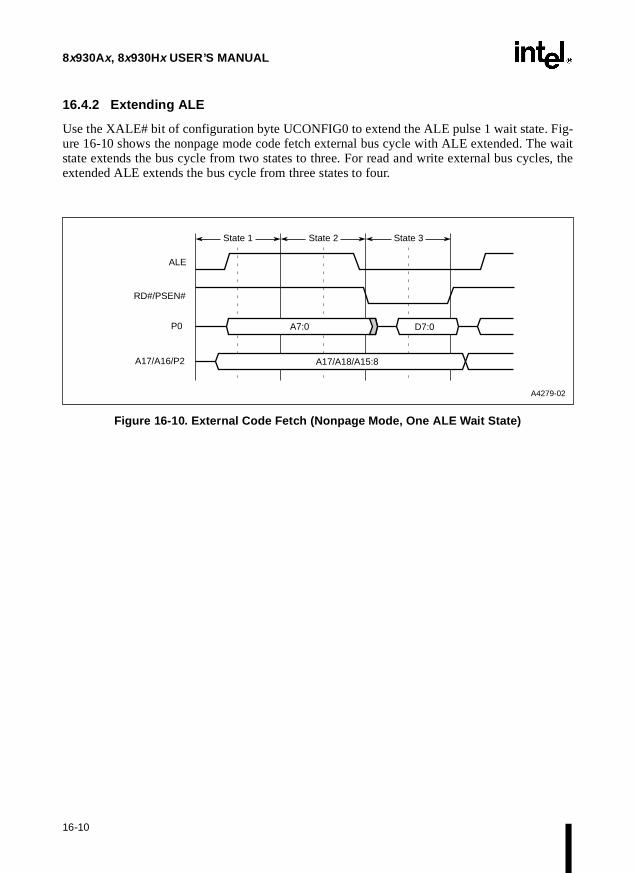
8x930Ax, 8x930Hx USER’S MANUAL
Fig-waitles, the
16.4.2 Extending ALE
Use the XALE# bit of configuration byte UCONFIG0 to extend the ALE pulse 1 wait state. ure 16-10 shows the nonpage mode code fetch external bus cycle with ALE extended. The state extends the bus cycle from two states to three. For read and write external bus cycextended ALE extends the bus cycle from three states to four.
Figure 16-10. External Code Fetch (Nonpage Mode, One ALE Wait State)
P0
A17/A16/P2
ALE
RD#/PSEN#
A4279-02
A7:0 D7:0
A17/A18/A15:8
State 1 State 2 State 3
16-10

EXTERNAL MEMORY INTERFACE
ol and en-igure
16.5 EXTERNAL BUS CYCLES WITH REAL-TIME WAIT STATES
There are two ways of using real-time wait states: the WAIT# pin used as an input bus contrthe WAIT# signal used in conjunction with the WCLK output signal. These two signals areabled with the WCON special function register in the SFR space at S:0A7H. Refer to F16-11.
NOTEThe WCLK and WAIT# signals are alternate functions for the port 1.7:6 input and output buffers. Use of the alternate functions may conflict with wait state operation.
When WAIT# is enabled, PCA module 3 is disabled on port 1.6 (CEX3) and resumes operation only when the WAIT# function is disabled. The same relationship exists between WCLK on port 1.7 (CEX4) and PCA module 4. It is not advisable to alternate between PCA operations and real-time wait-state operations at port 1.6 (CEX3/WAIT#) or port 1.7 (CEX4/WCLK).
Port 1.7 can also be configured to serve as address signal A17 (See UNCONFIG0 on page 4-5). The A17 address signal always takes priority over the alternate functions (CEX4 and WCLK). Even if RTWCE is enabled in WCON.1, the WCLK output does not appear during bus cycles enabled to drive address A17. The use of WAIT# as an input on port 1.6 is unaffected by address signals.
Figure 16-11. WCON: Real-time Wait State Control Register
WCON Address: S:A7HReset: xxxx xx00B
Wait State Control Register. Use this register to enable the real-time wait state input signal and/or the wait state output clock.
7 0
— — — — — — RTWCE RTWE
Bit Number
Bit Mnemonic Function
7:2 — Reserved:
The values read from these bits are indeterminate. Write “0” to these bits.
1 RTWCE Real-time WAIT CLOCK enable. Write a ‘1’ to this bit to enable the WAIT CLOCK on port 1.7 (WCLK). The square wave output signal is one-half the oscillator frequency.
0 RTWE Real-time WAIT# enable. Write a ‘1’ to this bit to enable real-time wait state input on port 1.6 (WAIT#).
16-11

8x930Ax, 8x930Hx USER’S MANUAL
aticro- of
bus
mod-hold
ee sig-withtput.
icts the
16.5.1 Real-time WAIT# Enable (RTWE)
The real-time WAIT# input is enabled by writing a logical ‘1’ to the WCON.0 (RTWE) bitS:A7H. During bus cycles, the external memory system can signal “system ready” to the mcontroller in real time by controlling the WAIT# input signal on the port 1.6 input. SamplingWAIT# is coincident with the activation of RD#/PSEN# or WR# signals driven low during a cycle. A “not-ready” condition is recognized by the WAIT# signal held at VIL by the externalmemory system. Use of PCA module 3 may conflict with your design. Do not use the PCA ule 3 I/O (CEX3) interchangeably with the WAIT# signal on the port 1.3 input. Setup and times are illustrated in the current datasheet.
16.5.2 Real-time WAIT CLOCK Enable (RTWCE)
The real-time WAIT CLOCK output is driven at port 1.7 (WCLK) by writing a logical ‘1’ to thWCON.1 (RTWCE) bit at S:A7H. When enabled, the WCLK output produces a square wavnal with a period of one-half the oscillator frequency. Use of PCA module 4 may conflict your design. Do not use the PCA module 4 I/O (CEX4) interchangeably with the WCLK ouUse of address signal A17 inhibits both WCLK and PCA module 4 usage of port 1.7.
16.5.3 Real-time Wait State Bus Cycle Diagrams
Figure 16-12 shows the code fetch/data read bus cycle in nonpage mode. Figure 16-14 depdata read cycle in page mode.
CAUTIONThe real-time wait function has critical external timing for code fetch. For this reason, it is not advisable to use the real-time wait feature for code fetch in page mode.
The data write bus cycle in nonpage mode is shown in Figure 16-13. Figure 16-15 shows the datawrite bus cycle in page mode.
16-12
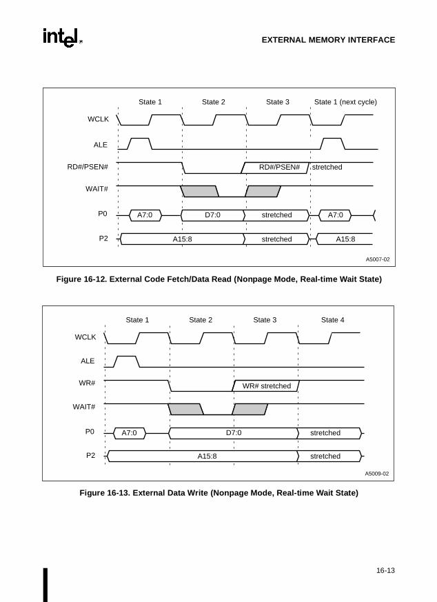
EXTERNAL MEMORY INTERFACE
Figure 16-12. External Code Fetch/Data Read (Nonpage Mode, Real-time Wait State)
Figure 16-13. External Data Write (Nonpage Mode, Real-time Wait State)
A7:0
WCLK
ALE
RD#/PSEN#
WAIT#
P0
P2 A15:8
A5007-02
State 1 State 2 State 3 State 1 (next cycle)
A7:0D7:0 stretched
A15:8 stretched
RD#/PSEN# stretched
A7:0
WCLK
ALE
WR#
WAIT#
P0
P2
A5009-02
State 1 State 2 State 3 State 4
D7:0 stretched
A15:8 stretched
WR# stretched
16-13

8x930Ax, 8x930Hx USER’S MANUAL
Figure 16-14. External Data Read ( Page Mode, Real-time Wait State)
Figure 16-15. External Data Write (Page Mode, Real-time W ait State)
A15:8
WCLK
ALE
RD#/PSEN#
WAIT#
P2
P0 A7:0
A5008-02
State 1 State 2 State 3 State 1 (next cycle)
A15:8D7:0 stretched
A7:0 stretched
RD#/PSEN# stretched
A15:8
WCLK
ALE
WR#
WAIT#
P2
P0
A5010-02
State 1 State 2 State 3 State 4
D7:0 stretched
A7:0 stretched
WR# stretched
16-14

EXTERNAL MEMORY INTERFACE
em-
-
eration, states P2s notpages
state.
d as theter 10,
16.6 CONFIGURATION BYTE BUS CYCLES
If EA# = 0, devices obtain configuration information from a configuration array in external mory. This section describes the bus cycles executed by the reset routine to fetch user configurationbytes from external memory. Configuration bytes are discussed in Chapter 4, “Device Configuration.”
To determine whether the external memory is set up for page mode or nonpage mode opthe 8x930 accesses external memory using internal address FF:FFF8H (UCONFIG0). See1–4 in Figure 16-16. If the external memory is set up for page mode, it places UCONFIG0 onas D7:0, overwriting A15:8 (FFH). If external memory is set up for nonpage mode, A15:8 ioverwritten. The 8x930 examines P2 bit 1. Subsequent configuration byte fetches are in mode if P2.1 = 0 and in nonpage mode if P2.1 = 1. The 8x930 fetches UCONFIG0 again (state5–8 in Figure 16-16) and then UCONFIG1 via internal address FF:FFF9H.
The configuration byte bus cycles always execute with ALE extended and one PSEN# wait
Figure 16-16. Configuration Byte Bus Cycles
16.7 PORT 0 AND PORT 2 STATUS
This section summarizes the status of the port 0 and port 2 pins when these ports are useexternal bus. A more comprehensive description of the ports and their use is given in Chap“Input/Output Ports.”
P0
P2
ALE
PSEN#
XTAL
A7:0 = F8H A7:0 = F8H A7:0 = F8H
A15:8 = FFH D7:0 D7:0A15:8 = FFH
Nonpage Mode
State 1
A4228-01
State 2 State 3 State 4 State 5 State 6 State 7 State 8
P0
P2
A7:0 = F8H D7:0
A15:8 = FFH
Page Mode
16-15

8x930Ax, 8x930Hx USER’S MANUAL
an orig-
e nd the
external
2 aremory.
lost. A at high
wever,to theexternalusrating
When port 0 and port 2 are used as the external memory bus, the signals on the port pins cinate from three sources:
• the 8x930 CPU (address bits, data bits)
• the port SFRs: P0 and P2 (logic levels)
• an external device (data bits)
The port 0 pins (but not the port 2 pins) can also be held in a high-impedance state. Tabl16-3lists the status of the port 0 and port 2 pins when the chip in is the normal operating mode aexternal bus is idle or executing a bus cycle.
16.7.1 Port 0 and Port 2 Pin Status in Nonpage Mode
In nonpage mode, the port pins have the same signals as those on the 8XC51FX. For an memory instruction using a 16-bit address, the port pins carry address and data bits during the buscycle. However, if the instruction uses an 8-bit address (e.g., MOVX @Ri), the contents of Pdriven onto the pins. These pin signals can be used to select 256-bit pages in external me
During a bus cycle, the CPU always writes FFH to P0, and the former contents of P0 are bus cycle does not change the contents of P2. When the bus is idle, the port 0 pins are heldimpedance, and the contents of P2 are driven onto the port 2 pins.
16.7.2 Port 0 and Port 2 Pin Status in Page Mode
In a page-mode bus cycle, the data is multiplexed with the upper address byte on port 2. Hoif the instruction uses an 8-bit address (e.g., MOVX @Ri), the contents of P2 are driven onpins when data is not on the pins. These logic levels can be used to select 256-bit pages in memory. During bus idle, the port 0 and port 2 pins are held at high impedance. For port pin statwhen the chip in is idle mode, powerdown mode, or reset, see Chapter 15, “Special OpeModes.”
Table 16-3. Port 0 and Port 2 Pin Status In Normal Operating Mode
Port 8-bit/16-bit Addressing
Nonpage Mode Page Mode
Bus Cycle Bus Idle Bus Cycle Bus Idle
Port 0 8 or 16 AD7:0 (1) High Impedance A7:0 (1) High Impedance
Port 2 8 P2 (2) P2 P2/D7:0 (2) High Impedance
16 A15:8 P2 A15:8/D7:0 High Impedance
NOTES:1. During external memory accesses, the CPU writes FFH to the P0 register and the register
contents are lost.2. The P2 register can be used to select 256-byte pages in external memory.
16-16
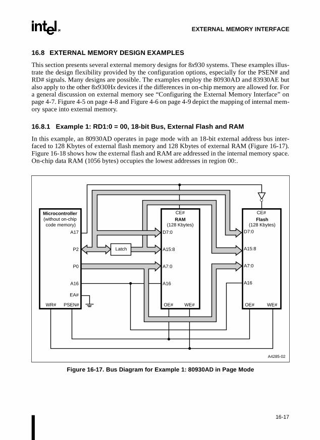
EXTERNAL MEMORY INTERFACE
- and
ore” onl mem-
-17).ace.
16.8 EXTERNAL MEMORY DESIGN EXAMPLES
This section presents several external memory designs for 8x930 systems. These examples illustrate the design flexibility provided by the configuration options, especially for the PSEN#RD# signals. Many designs are possible. The examples employ the 80930AD and 83930AE butalso apply to the other 8x930Hx devices if the differences in on-chip memory are allowed for. Fa general discussion on external memory see “Configuring the External Memory Interfacpage 4-7. Figure 4-5 on page 4-8 and Figure 4-6 on page 4-9 depict the mapping of internaory space into external memory.
16.8.1 Example 1: RD1:0 = 00, 18-bit Bus, External Flash and RAM
In this example, an 80930AD operates in page mode with an 18-bit external address bus inter-faced to 128 Kbytes of external flash memory and 128 Kbytes of external RAM (Figure 16Figure 16-18 shows how the external flash and RAM are addressed in the internal memory spOn-chip data RAM (1056 bytes) occupies the lowest addresses in region 00:.
Figure 16-17. Bus Diagram for Example 1: 80930AD in Page Mode
Microcontroller (without on-chip code memory)
A17
P2
P0
A16
EA#
WR# PSEN#
CE#
D7:0 A15:8 A7:0 A16
OE# WE#
CE#
D7:0 A15:8 A7:0 A16
OE# WE#
RAM (128 Kbytes)
Flash (128 Kbytes)
Latch
A4285-02
16-17
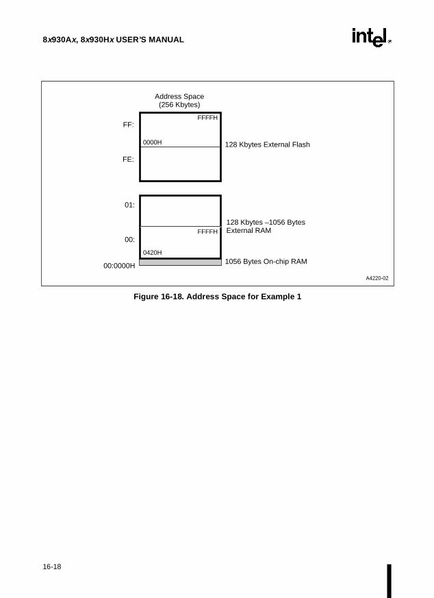
8x930Ax, 8x930Hx USER’S MANUAL
Figure 16-18. Address Space for Example 1
A4220-02
1056 Bytes On-chip RAM
01:
00:
FE:
FF:
128 Kbytes External Flash
Address Space (256 Kbytes)
0000H
FFFFH
0420H
FFFFH128 Kbytes –1056 Bytes External RAM
00:0000H
16-18

EXTERNAL MEMORY INTERFACE
6ternaln-chip
16.8.2 Example 2: RD1:0 = 01, 17-bit Bus, External Flash and RAM
In this example, an 80930AD operates in page mode with a 17-bit external address bus interfacedto 64 Kbytes of flash memory for code storage and 32 Kbytes of external RAM (Figure 16-19).The 80930AD is configured so that PSEN# is asserted for all reads, and RD# functions as A1(RD1:0 = 01). Figure 16-20 shows how the external flash and RAM are addressed in the inmemory space. Addresses 0420H–7FFFH in external RAM are addressed in region 00:. Odata RAM (1056 bytes) occupies the lowest addresses in region 00:.
Figure 16-19. Bus Diagram for Example 2: 80930AD in Page Mode
PSEN#WR#
RAM (32 Kbytes)
OE#
FLASH (64 Kbytes)
OE# WE#WE#
CE# CE#
A15:8/D7:0 A15:8
P2
P0
EA#
D7:0
A15:8
A7:0
A15:8
A7;0
D7:0A16
A7:0
Latch
Data Code
A4286-02
Microcontroller (without on-chip code memory)
16-19

8x930Ax, 8x930Hx USER’S MANUAL
-
Figure 16-20. Address Space for Example 2
16.8.3 Example 3: RD1:0 = 01, 17-bit Bus, External RAM
In this example, an 83930AE operates in nonpage mode with a 17-bit external address bus interfaced to 128 Kbytes of external RAM (Figure 16-21). The 83930AE is configured so that RD#functions as A16, and PSEN# is asserted for all reads. Figure 16-22 shows how the external RAMis addressed in the internal memory space.
A4168-03
1056 Bytes On-chip RAM
01:
00:
FE:
FF: 64 Kbytes External Flash
Address Space (256 Kbytes)
0000H
FFFFH
0420H32 Kbytes –1056 Bytes External RAM
00:0000H
7FFFH
16-20

EXTERNAL MEMORY INTERFACE
Figure 16-21. Bus Diagram for Example 3: 83930AE in Nonpage Mode
PSEN#
A5004-01
WR#
D7:0
A15:8
A7:0
A16
OE# WE#
A15:8
A16
P2
P0
A7:0
Microcontroller (with on-chip
code memory)
RAM (128 Kbytes)
CE#EA#
VCC
AD7:0
Latch
A16
Data
16-21

8x930Ax, 8x930Hx USER’S MANUAL
Figure 16-22. Memory Space for Example 3
A4169-03
1056 Bytes On-chip RAM
01:
00:
FE:
FF:
16 Kbytes On-chip Code Memory
Address Space (256 Kbytes)
0000H
FFFFH
0420H
FFFFH
128 Kbytes –1056 Bytes External RAM
00:0000H
3FFFH
16-22

EXTERNAL MEMORY INTERFACE
-ed alligure
16.8.4 Example 4: RD1:0 = 10, 16-bit Bus, External RAM
In this example, an 83930AE operates in nonpage mode with a 16-bit external address bus interfaced to 64 Kbytes of RAM (Figure 16-23). This configuration leaves P3.7/RD#/A16 availablfor general I/O (RD1:0 = 10). A maximum of 64 Kbytes of external memory can be used anregions of internal memory map into the single 64-Kbyte region in external memory (see F4-6 on page 4-9). Figure 16-24 shows how the external RAM is addressed in the internal memoryspace. User code is stored in on-chip ROM.
Figure 16-23. Bus Diagram for Example 4: 83930AE in Nonpage Mode
PSEN#
A5005-01
WR#
D7:0
A15:8
A7:0
OE# WE#
P2
P0
Microcontroller (with on-chip
code memory)
RAM (64 Kbytes)
CE#EA#
VCC
Latch
16-23

8x930Ax, 8x930Hx USER’S MANUAL
Figure 16-24. Address Space for Example 4
A4224-02
1056 Bytes On-chip RAM
01:
00:
FE:
FF:
16 Kbytes On-chip Code Memory
Address Space (256 Kbytes)
FFFFH
0420H
FFFFHExternal RAM 64 Kbytes – 1056 Bytes
00:0000H
0000H 3FFFH
16-24

EXTERNAL MEMORY INTERFACE
r-
mem-
ddressntll that
s haveare
ip datae
can be If theternal
16.8.5 Example 5: RD1:0 = 11, 16-bit Bus, External EPROM and RAM
In this example, an 80930AD operates in nonpage mode with a 16-bit external address bus intefaced to 64 Kbytes of EPROM and 64 Kbytes of RAM (Figure 16-25). The 80930AD is config-ured so that RD# is asserted for addresses ≤ 7F:FFFFH and PSEN# is asserted for addresses ≥ 80:0000H. Figure 16-26 shows two ways to address the external memory in the internalory space.
Addressing external RAM locations in either region 00: or region 01: produces the same aat the external bus pins. However, if the external EPROM and the external RAM require differenumbers of wait states, the external RAM must be addressed entirely in region 01:. Recathe number of wait states for region 01: is independent of the remaining regions and alwaythe same number of wait states (see Table 4-3 on page 4-11) unless the real-time wait states selected (see Figure 16-11 on page 16-11).
The examples that follow illustrate two possibilities for addressing the external RAM.
16.8.5.1 An Application Requiring Fast Access to the Stack
If an application requires fast access to the stack, the stack can reside in the fast on-chRAM (00:0020H–00:041FH) and, when necessary, roll out into the slower external RAM. See thleft side of Figure 16-26. In this case, the external RAM can have wait states only if the EPROMhas wait states. Otherwise, if the stack rolls out above location 00:041FH, the external RAMwould be accessed with no wait state.
16.8.5.2 An Application Requiring Fast Access to Data
If fast access to a block of data is more important than fast access to the stack, the datastored in the on-chip data RAM, and the stack can be located entirely in external memory.external RAM requires a different number of wait states than the EPROM, address the exRAM entirely in region 01:. See the right side of Figure 16-26. Addresses above 00:041FH rollout to external memory beginning at 0420H.
16-25

8x930Ax, 8x930Hx USER’S MANUAL
Figure 16-25. Bus Diagram for Example 5: 80930AD in Nonpage Mode
A7:0
Latch
A15:8
A/D7:0
EPROM (64 Kbytes)
OE#
CE#
A15:8
A7:0
D7:0
PSEN#
Microcontroller (without on-chip code memory)
RD#WR#
EA#
P2
P0
D7:0
A15:8
A7:0
RAM (64 Kbytes)
CE#
OE# WE#
DataCode
A4287-02
16-26
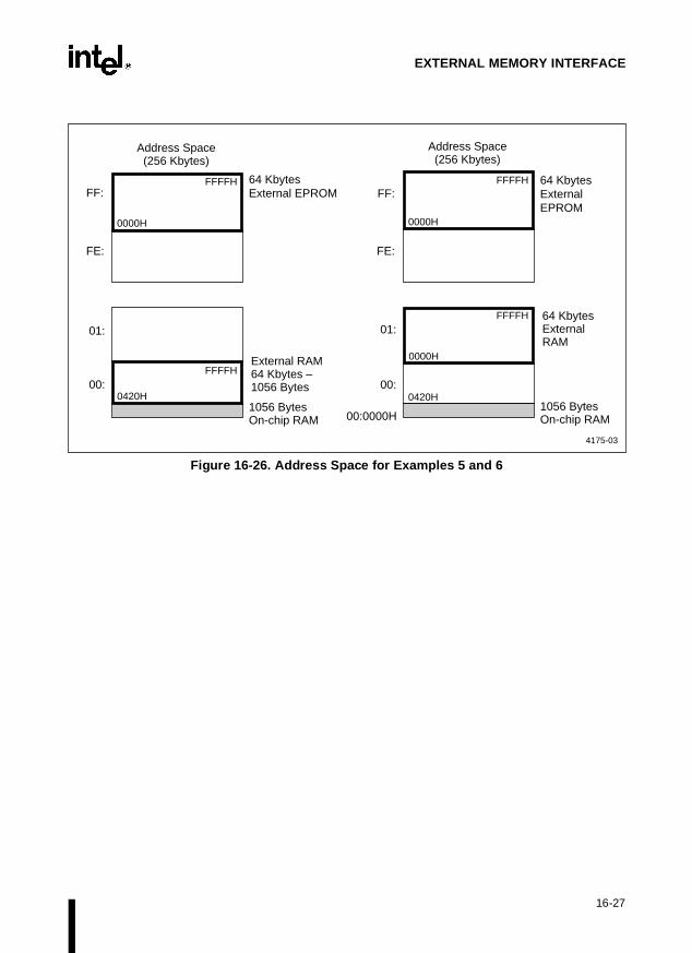
EXTERNAL MEMORY INTERFACE
Figure 16-26. Address Space for Examples 5 and 6
1056 Bytes On-chip RAM
01:
00:
FE:
FF:64 Kbytes External EPROM
Address Space (256 Kbytes)
0000H
FFFFH
0420H
FFFFHExternal RAM 64 Kbytes – 1056 Bytes
1056 Bytes On-chip RAM
01:
00:
FE:
FF:64 Kbytes External EPROM
Address Space (256 Kbytes)
0000H
FFFFH
0420H
64 Kbytes External RAM
00:0000H
FFFFH
0000H
4175-03
16-27

8x930Ax, 8x930Hx USER’S MANUAL
- on ad-
16.8.6 Example 6: RD1:0 = 11, 16-bit Bus, External EPROM and RAM
In this example, an 80930AD operates in page mode with a 16-bit external address bus interfacedto 64 Kbytes of EPROM and 64 Kbytes of RAM (Figure 16-27). The 80930AD is configured sothat RD# is asserted for addresses ≤ 7F:FFFFH, and PSEN# is asserted for addresses ≥ 80:0000.
This system is the same as Example 5 (Figure 16-25) except that it operates in page mode. Accordingly, the two systems have the same memory map (Figure 16-26), and the commentsdressing external RAM apply here also.
Figure 16-27. Bus Diagram for Example 6: 80930AD in Page Mode
A7:0
A15:8/D7:0 A15:8
Latch
PSEN#
Microcontroller (without on-chip code memory)
RD#WR#
P2
P0
EA#
EPROM (64 Kbytes)
OE#
D7:0
A15:8
A7:0
CE# CE#
A15:8
A7;0
RAM (64 Kbytes)
D7:0
OE# WE#
Code Data
A4288-02
16-28

EXTERNAL MEMORY INTERFACE
:0)
inter-
16.8.7 Example 7: RD1:0 = 01, 17-bit Bus, External Flash
In this example, an 80930AD operates in page mode with a 17-bit external address bus interfacedto 128 Kbytes of flash memory (Figure 16-28). Port 2 carries both the upper address bits (A15and the data (D7:0), while port 0 carries only the lower address bits (A7:0). The 80930AD is con-figured for a single read signal (PSEN#). The 128 Kbytes of external flash are accessed vianal memory regions FE: and FF: in the internal memory space.
Figure 16-28. Bus Diagram for Example 7: 80930AD in Page Mode
PSEN#
Microcontroller (without on-chip code memory)
WR#
FLASH (128 Kbytes)
OE# WE#
A15:8/D7:0 A15:8
P2
P0
A15:8
A7:0
A7:0
Latch
D7:0
A16
CE#
A16
EA#
A16
Code
A4289-02
16-29


17Verifying Nonvolatile Memory


ed in
. Ver-e, in-
r lowete list
he
tion
e: fort in-gram
1 andhigheston,
devicet .
CHAPTER 17VERIFYING NONVOLATILE MEMORY
This chapter provides instructions for verifying on-chip nonvolatile memory on the 8x930. Theverify instructions permit reading memory locations to verify their contents. Features coverthis chapter are:
• verifying the on-chip program code memory (8 Kbytes, 16 Kbytes)
• verifying the on-chip configuration bytes (8 bytes)
• verifying the lock bits (3 bits)
• using the encryption array (128 bytes)
• verifying the signature bytes (3 bytes)
17.1 GENERAL
The 8x930 is verified in the same manner as the 87C51FX and 87C251Sx microcontrollersify operations differ from normal operation. Memory accesses are made one byte at a timput/output port assignments are different, and ALE, EA#, and PSEN# are held high oexternally. See Tables 17-1 and 17-2 for lead usage during verify operations. For a complof device signal descriptions, see Appendix B.
In some applications, it is desirable that program code be secure from unauthorized access. T8x930 offers two types of protection for program code stored in the on-chip array:
• Program code in the on-chip code memory area is encrypted when read out for verificaif the encryption array is programmed.
• A three-level lock bit system restricts external access to the on-chip program code memory.
17.1.1 Considerations for On-chip Program Code Memory
On-chip, nonvolatile code memory is located at the lower end of the FF: region. (Exampldevices with 16 Kbytes of ROM, code memory is located at FF:0000H-FF:3FFFH.) The firsstruction following device reset is fetched from FF:0000H. It is recommended that user procode start at address FF:0100H. Use a jump instruction to FF:0100H to begin execution of theprogram. For information on address spaces, see Chapter 3, “Address Spaces.”
Addresses outside the range of on-chip code memory access external memory. With EA# =both on-chip and external code memory implemented, you can place program code at the on-chip memory addresses. When the highest on-chip address is exceeded during executipro-gram code fetches automatically rollover from on-chip memory to external memory. See the dualnote on page 3-8.
The top eight bytes of the memory address space (FF:FFF8H–FF:FFFFH) are reserved forconfiguration. Do not read or write program code at these locations. For EA# = 1, the reserou-tine obtains configuration information from a configuration array located these addresses(For
17-1

8x930Ax, 8x930Hx USER’S MANUAL
xter-on, see
sddressressesote on
EA# = 0, the reset routine obtains configuration information from a configuration array in enal memory using these internal addresses.) For a detailed discussion of device configuratiChapter 4, “Device Configuration”.
With EA# = 1 and only on-chip program code memory, multi-byte instructions and instructionthat result in call returns or prefetches should be located a few bytes below the maximum ato avoid inadvertently exceeding the top address. Use an EJMP instruction, five or more addbelow the top of memory, to continue execution in other areas of memory. See the dual npage 3-8
CAUTIONExecution of program code located in the top few bytes of the on-chip memory may cause prefetches from the next higher addresses (i.e., external memory). External memory fetches make use of port 0 and port 2 and may disrupt program execution if the program uses port 0 or port 2 for a different purpose.
.
Table 17-1. Signal Descriptions
Signal Name Type Description Alternate
Function
P0.7:0 I/O Port 0 . Eight-bit, open-drain, bidirectional I/O port. For verify operations, use to specify the verify mode. See Table 17-2 and Figures 17-1 and 17-2.
AD7:0
P1.0P1.1P1.2P1.5:3P1.6P1.7
I/O Port 1 . Eight-bit, bidirectional I/O port with internal pullups. For verify operations, use for high byte of address. See Table 17-2 and Figures 17-1 and 17-2.
T2T2EXECICEX2:0CEX3/WAIT#CEX4/A17\WCLK
P2.7:0 I/O Port 2 . Eight-bit, bidirectional I/O port with internal pullups. For verify operations, use as the data port. See Table 17-2 and Figures 17-1 and 17-2.
A15:8
P3.0P3.1P3.3:2P3.5:4P3.6P3.7
I/O Port 3 . Eight-bit, bidirectional I/O port with internal pullups. For verify operations, use for low byte of address. See Table 17-2 and Figures 17-1 and 17-2.
RXDTXDINT1:0#T1:0WR#RD#/A16
ALE — Address Latch Enable. For verify operations, connect this pin to VCC
—
EA# — External Enable. For verify operations, connect this pin to VCC —
PSEN# — Program Store Enable . For verify operations, connect this pin to VSS
—
17-2

VERIFYING NONVOLATILE MEMORY
port
essesyptions
ex-
r ast 2. Con-
17.2 VERIFY MODES
Table 17-2 lists the verify modes and provides details about the setup. The value applied to0 determines the mode. The upper digit specifies verify and the lower digit selects the memoryfunction to verify (e.g., on-chip program code memory, configuration bytes, etc.). The addrapplied to port 1 and port 3 address locations in the selected memory function. The encrarray, lock bits, and signature bytes reside in nonvolatile memory outside the memory addresspace. Configuration bytes, UCONFIG0 and UCONFIG1, reside in nonvolatile memory at the topof the memory address space (Figure 4-1 on page 4-2) for devices with on-chip ROM, and internal memory as shown in (Figure 4-2 on page 4-3) for devices without on-chip ROM.
17.3 GENERAL SETUP
Figure 17-1 shows the general setup for verifying nonvolatile memory on the 8x930. The control-ler must be running with an oscillator frequency of 4 MHz to 6 MHz. Set up the controlleshown in Table 17-2 with the mode of operation specified on port 0 and the address with respecto the starting address of the memory area applied to ports 1 and 3. Data appears on portnect RST, ALE, and EA# to VCC and PSEN# to ground.
Figure 17-2 shows the bus cycle waveforms for the verify operations. Timing symbols are definedin Table 17-5 on page 17-6.
Table 17-2. Verify Modes
Mode RST PSEN# EA# ALE Port0
Port2
AddressPort 1 (high)Port 3 (low)
Notes
Verify Mode. On-chip program code Memory
High Low 5 V High 28H data 0000H-3FFFH 1
Verify Mode. Configuration Bytes (UCONFIG0, UCONFIG1)
High Low 5 V High 29H data FFF8H-FFFFH 1
Verify Mode. Lock bits High Low 5 V High 2BH data 0000H 2
Verify Mode. Signature Bytes
High Low 5 V High 29H data0030H, 0031H,0060H, 0061H
NOTES:1. For these modes, the internal address is FF:xxxxH.2. The three lock bits are verified in a single operation. The states of the lock bits appear simultaneously
at port 2 as follows: LB3 - P2.3, LB2 - P2.2. LB1 - P2.1. High = programmed.
17-3
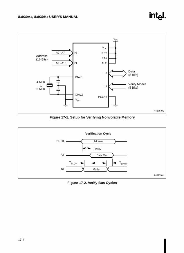
8x930Ax, 8x930Hx USER’S MANUAL
Figure 17-1. Setup for Verifying Nonvolatile Memory
Figure 17-2. Verify Bus Cycles
PSEN#
P1
P2
A4376-01
4 MHz to
6 MHz
XTAL2
A0 - A7
A8 - A15
P3
P1
Data (8 Bits)
VSS
VCC
VCC
XTAL1
Verify Modes (8 Bits)
Address (16 Bits) EA#
RST
ALE
P1, P3
A4377-01
Address
P0
P2 Data Out
Mode
Verification Cycle
TELQV
TAVQV
TEHQV
17-4

VERIFYING NONVOLATILE MEMORY
k bitsyteck of
7-2.
y
-orderis read, ar-
de is
17.4 VERIFY ALGORITHM
Use this procedure to verify program code, signature bytes, configuration bytes, and locstored in nonvolatile memory on the 8x930. To preserve the secrecy of the encryption key bsequence, the encryption array cannot be verified. Verification can be performed on a blobytes. The procedure for verifying the 8x930 is as follows:
1. Set up the microcontroller for operation in the appropriate mode according to Table 1
2. Input the 16-bit address on ports P1 and P3.
3. Wait for the data on port P2 to become valid (TAVQV = 48 clock cycles, Figure 17-5), thencompare the data with the expected value.
4. Repeat steps 1 through 3 until all memory locations are verified.
17.5 LOCK BIT SYSTEM
The 8x930 provides a three-level lock system for protecting program code stored in the on-chipprogram code memory from unauthorized access. To verify that the lock bits are correctlpro-grammed, perform the procedure described in “Verify Algorithm” on page 17-5 using the verifylock bits mode (Table 17-2).
17.5.1 Encryption Array
The 8x930 includes a 128-byte encryption array located in nonvolatile memory outside the mem-ory address space. During verification of the on-chip program code memory, the seven lowaddress bits also address the encryption array. As the byte of the program code memory it is exclusive-NORed (XNOR) with the key byte from the encryption array. If the encryptionray is not programmed (still all 1s), the program code is placed on the data bus in its original, un-encrypted form. If the encryption array is programmed with key bytes, the program coencrypted and can not be used without knowledge of the key byte sequence.
Table 17-3. Lock Bit Function
Lock Bits Programmed Protection Type
LB3 LB2 LB1
Level 1 U U U No program lock features are enabled. On-chip program code is encrypted when verified, if encryption array is programmed.
Level 2 U U P External program code is prevented from fetching program code bytes from on-chip code memory.
Level 3 U P P Same as level 2, plus on-chip program code memory verify is disabled.
Level 4 P P P Same as level 3, plus external memory execution is disabled.
NOTE: Other combinations of the lock bits are not defined.
17-5

8x930Ax, 8x930Hx USER’S MANUAL
nature
CAUTIONIf the encryption feature is implemented, the portion of the on-chip program code memory that does not contain program code should be filled with “random” byte values other than FFH to prevent the encryption key sequence from being revealed. To preserve the secrecy of the encryption key byte sequence, the encryption array cannot be verified.
17.6 SIGNATURE BYTES
The 8x930 contains factory-programmed signature bytes. These bytes are located in nonvolatilememory outside the memory address space at 30H, 31H, 60H, and 61H. To read the sigbytes, perform the procedure described in “Verify Algorithm” on page 17-5 using the verify sig-nature mode (Table 17-2). Signature byte values are listed in Table 17-4.
Table 17-4. Contents of the Signature Bytes
ADDRESS CONTENTS DEVICE TYPE
30H 89H Indicates Intel devices
31H 41H Indicates USB core product
60H TBD Indicates 8x930 device
Table 17-5. Timing Definitions
Symbol Definition
1/TCLCL Oscillator Frequency
TAVQV Address to Data Valid
TEHQZ Data Float after ENABLE
TELQV ENABLE Low to Data Valid
NOTE: A = Address, E = Enable, H = High, L = Low,Q = Data out, V = Valid, Z = Floating
17-6

AInstruction Set Reference

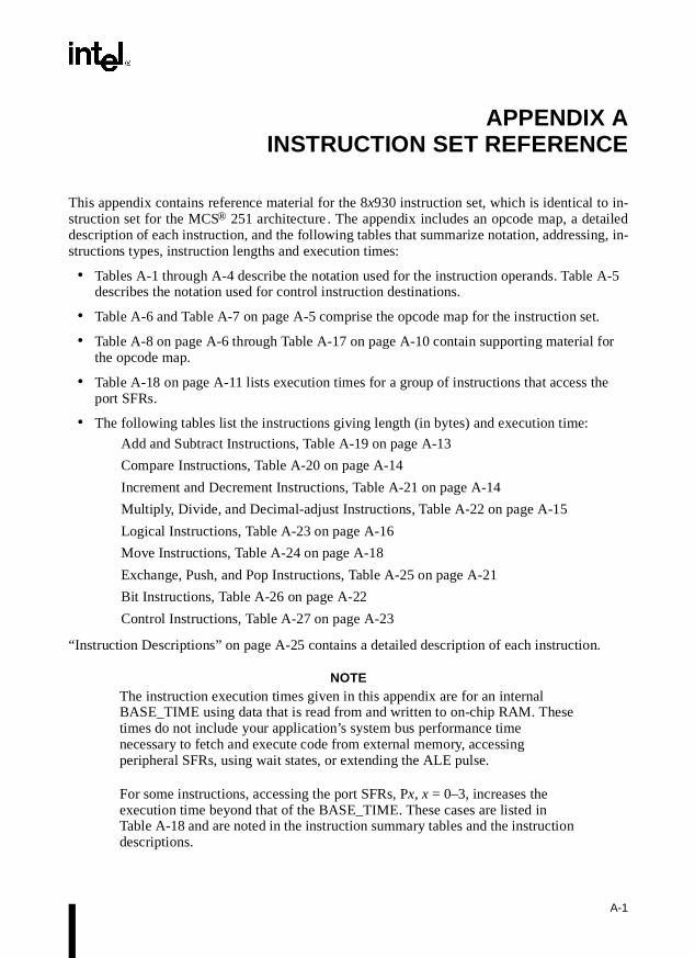
-dng, in-
-5
.
for
he
.
APPENDIX AINSTRUCTION SET REFERENCE
This appendix contains reference material for the 8x930 instruction set, which is identical to instruction set for the MCS® 251 architecture . The appendix includes an opcode map, a detailedescription of each instruction, and the following tables that summarize notation, addressistructions types, instruction lengths and execution times:
• Tables A-1 through A-4 describe the notation used for the instruction operands. Table Adescribes the notation used for control instruction destinations.
• Table A-6 and Table A-7 on page A-5 comprise the opcode map for the instruction set
• Table A-8 on page A-6 through Table A-17 on page A-10 contain supporting material the opcode map.
• Table A-18 on page A-11 lists execution times for a group of instructions that access tport SFRs.
• The following tables list the instructions giving length (in bytes) and execution time:
Add and Subtract Instructions, Table A-19 on page A-13
Compare Instructions, Table A-20 on page A-14
Increment and Decrement Instructions, Table A-21 on page A-14
Multiply, Divide, and Decimal-adjust Instructions, Table A-22 on page A-15
Logical Instructions, Table A-23 on page A-16
Move Instructions, Table A-24 on page A-18
Exchange, Push, and Pop Instructions, Table A-25 on page A-21
Bit Instructions, Table A-26 on page A-22
Control Instructions, Table A-27 on page A-23
“Instruction Descriptions” on page A-25 contains a detailed description of each instruction
NOTEThe instruction execution times given in this appendix are for an internal BASE_TIME using data that is read from and written to on-chip RAM. These times do not include your application’s system bus performance time necessary to fetch and execute code from external memory, accessing peripheral SFRs, using wait states, or extending the ALE pulse.
For some instructions, accessing the port SFRs, Px, x = 0–3, increases the execution time beyond that of the BASE_TIME. These cases are listed in Table A-18 and are noted in the instruction summary tables and the instruction descriptions.
A-1

8x930Ax, 8x930Hx USER’S MANUAL
A.1 NOTATION FOR INSTRUCTION OPERANDS
Table A-1. Notation for Register Operands
Register Notation 8x930 MCS 51Arch.
@Ri A memory location (00H–FFH) addressed indirectly via byte registerR0 or R1 4
Rn Byte register R0–R7 of the currently selected register bank
n Byte register index: n = 0–7
r r r Binary representation of n
4
Rm Byte register R0–R15 of the currently selected register file
Rmd Destination register
Rms Source register
m, md, ms Byte register index: m, md, ms = 0–15
s s s s Binary representation of m or md
S S S S Binary representation of ms
4
WRj Word register WR0, WR2, ..., WR30 of the currently selected registerfile
WRjd Destination register
WRjs Source register
@WRj A memory location (00:0000H–00:FFFFH) addressed indirectlythrough word register WR0–WR30
@WRj Data RAM location (00:0000H–00:FFFFH) addressed indirectly+dis16 through a word register (WR0–WR30) + displacement value, where
the displacement value is from 0 to 64 Kbytes.
j, jd, js Word register index: j, jd, js = 0–30
t t t t Binary representation of j or jd
T T T T Binary representation of js
4
DRk Dword register DR0, DR4, ..., DR28, DR56, DR60 of the currentlyselected register file
DRkd Destination Register
DRks Source Register
@DRk A memory location (00:0000H–FF:FFFFH) addressed Indirectlythrough dword register DR0–DR28, DR56, DR60
@DRk Data RAM location (00:0000H–FF:FFFFH) addressed indirectly+dis24 through a dword register (DR0–DR28, DR56, DR60) + displacement
value, where the displacement value is from 0 to 64 Kbytes
k, kd, ks Dword register index: k, kd, ks = 0, 4, 8, ..., 28, 56, 60
u u u u Binary representation of k or kd
U U U U Binary representation of ks
4
A-2

INSTRUCTION SET REFERENCE
Table A-2. Notation for Direct Addresses
DirectAddress. Description 8x930
Arch.MCS 51Arch.
dir8 An 8-bit direct address. This can be a memory address(00:0000H–00:007FH) or an SFR address (S:00H - S:FFH). 4 4
dir16 A 16-bit memory address (00:0000H–00:FFFFH) used in direct addressing. 4
Table A-3. Notation for Immediate Addressing
ImmediateData Description 8x930
Arch.MCS 51Arch.
#data An 8-bit constant that is immediately addressed in an instruction. 4 4
#data16 A 16-bit constant that is immediately addressed in an instruction. 4
#0data16#1data16
A 32-bit constant that is immediately addressed in an instruction. The upper word is filled with zeros (#0data16) or ones (#1data16). 4
#short
v v
A constant, equal to 1, 2, or 4, that is immediately addressed in an instruction.
Binary representation of #short.4
Table A-4. Notation for Bit Addressing
BitAddress Description 8x930
Arch.MCS 51Arch.
bit
y y y
A directly addressed bit in memory locations 00:0020H–00:007FH or in any defined SFR.A binary representation of the bit number (0–7) within a byte.
4
bit51 A directly addressed bit (bit number = 00H–FFH) in memory or an SFR. Bits 00H–7FH are the 128 bits in byte locations 20H–2FH in the on-chip RAM. Bits 80H–FFH are the 128 bits in the 16 SFR’s with addresses that end in 0H or 8H: S:80H, S:88H, S:90H, . . . , S:F0H, S:F8H.
4
Table A-5. Notation for Destinations in Control Instructions
DestinationAddress Description 8x930
Arch.MCS 51Arch.
rel A signed (two's complement) 8-bit relative address. The destination is -128 to +127 bytes relative to first byte of the next instruction. 4 4
addr11 An 11-bit destination address. The destination is in the same 2-Kbyte block of memory as the first byte of the next instruction. 4 4
addr16 A 16-bit destination address. A destination can be anywhere within the same 64-Kbyte region as the first byte of the next instruction. 4 4
addr24 A 24-bit destination address. A destination can be anywhere within the 16-Mbyte address space. 4
A-3

8x930Ax, 8x930Hx USER’S MANUAL
A.2 OPCODE MAP AND SUPPORTING TABLES
Table A-6. Instructions for MCS ® 51 Microcontrollers
Bin 0 1 2 3 4 5 6-7 8-F
Src 0 1 2 3 4 5 A5 x6–A5x7 A5x8–A5xF
0 NOP AJMPaddr11
LJMPaddr16
RRA
INCA
INCdir8
INC@Ri
INCRn
1 JBCbit,rel
ACALLaddr11
LCALLaddr16
RRCA
DECA
DECdir8
DEC@Ri
DECRn
2 JBbit,rel
AJMPaddr11
RET RLA ADDA,#data
ADDA,dir8
ADDA,@Ri
ADDA,Rn
3 JNBbit,rel
ACALLaddr11
RETI RLCA ADDCA,#data
ADDCA,dir8
ADDCA,@Ri
ADDCA,Rn
4 JCrel
AJMPaddr11
ORLdir8,A
ORLdir8,#data
ORLA,#data
ORLA,dir8
ORLA,@Ri
ORLA,Rn
5 JNCrel
ACALLaddr11
ANLdir8,A
ANLdir8,#data
ANLA,#data
ANLA,dir8
ANLA,@Ri
ANLA,Rn
6 JZrel
AJMPaddr11
XRLdir8,A
XRLdir8,#data
XRLA,#data
XRLA,dir8
XRLA,@Ri
XRLA,Rn
7 JNZrel
ACALLaddr11
ORLCY,bit
JMP@A+DPTR
MOVA,#data
MOVdir8,#data
MOV@Ri,#data
MOVRn,#data
8 SJMPrel
AJMPaddr11
ANLCY,bit
MOVCA,@A+PC
DIVAB
MOVdir8,dir8
MOVdir8,@Ri
MOVdir8,Rn
9 MOVDPTR,#data16
ACALLaddr11
MOVbit,CY
MOVCA,@A+DPTR
SUBBA,#data
SUBBA,dir8
SUBBA,@Ri
SUBBA,Rn
A ORLCY,bit
AJMPaddr11
MOVCY,bit
INCDPTR
MULAB
ESC MOV@Ri,dir8
MOVRn,dir8
B ANLCY,bit
ACALLaddr11
CPLbit
CPLCY
CJNEA,#data,rel
CJNEA,dir8,rel
CJNE@Ri,#data,rel
CJNERn,#data,rel
C PUSHdir8
AJMPaddr11
CLRbit
CLRCY
SWAPA
XCHA,dir8
XCHA,@Ri
XCHA,Rn
D POPdir8
ACALLaddr11
SETBbit
SETBCY
DAA
DJNZdir8,rel
XCHDA,@Ri
DJNZRn,rel
E MOVXA,@DPTR
AJMPaddr11
MOVXA,@Ri
CLRA
MOVA,dir8
MOVA,@Ri
MOVA,Rn
F MOV@DPTR,A
ACALLaddr11
MOVX@Ri,A
CPLA
MOVdir8,A
MOV@Ri,A
MOVRn,A
A-4
INSTRUCTION SET REFERENCE
Table A-7. Instructions for the 8x930 Architecture
Bin A5 x8 A5x9 A5xA A5 xB A5xC A5xD A5xE A5xF
Src x8 x9 xA xB xC xD xE xF
0 JSLErel
MOVRm,@WRj+dis
MOVZWRj,Rm
INC R,#short (1)MOV reg,ind
SRAreg
1 JSGrel
MOV@WRj+dis,Rm
MOVSWRj,Rm
DEC R,#short (1)MOV ind,reg
SRLreg
2 JLErel
MOVRm,@DRk+dis
ADDRm,Rm
ADDWRj,WRj
ADDreg,op2 (2)
ADDDRk,DRk
3 JGrel
MOV@DRk+dis,Rm
SLLreg
4 JSLrel
MOVWRj,@WRj+dis
ORLRm,Rm
ORLWRj,WRj
ORLreg,op2 (2)
5 JSGErel
MOV@WRj+dis,WRj
ANLRm,Rm
ANLWRj,WRj
ANLreg,op2 (2)
6 JErel
MOVWRj,@DRk+dis
XRLRm,Rm
XRLWRj,WRj
XRLreg,op2 (2)
7 JNErel
MOV@DRk+dis,WRj
MOVop1,reg (2)
MOVRm,Rm
MOVWRj,WRj
MOVreg,op2 (2)
MOVDRk,DRk
8 LJMP @WRjEJMP @DRk
EJMPaddr24
DIVRm,Rm
DIVWRj,WRj
9 LCALL@WRjECALL @DRk
ECALLaddr24
SUBRm,Rm
SUBWRj,WRj
SUBreg,op2 (2)
SUBDRk,DRk
A BitInstructions (3)
ERET MULRm,Rm
MULWRj,WRj
B TRAP CMPRm,Rm
CMPWRj,WRj
CMPreg,op2 (2)
CMPDRk,DRk
C PUSH op1 (4)MOV DRk,PC
D POPop1 (4)
E
F
NOTES:1. R = Rm/WRj/DRk.2. op1, op2 are defined in Table A-8.3. See Tables A-10 and A-11.4. See Table A-12.
A-5

8x930Ax, 8x930Hx USER’S MANUAL
Table A-8. Data Instructions
Instruction Byte 0 Byte 1 Byte 2 Byte 3
Oper Rmd,Rms x C md ms
Oper WRjd,WRjs x D jd/2 js/2
Oper DRkd,DRks x F kd/4 ks/4
Oper Rm,#data x E m 0000 #data
Oper WRj,#data16 x E j/2 0100 #data (high) #data (low)
Oper DRk,#data16 x E k/4 1000 #data (high) #data (low)
MOV DRk(h),#data16
MOV DRk,#1data16
CMP DRk,#1data16
7
7
B
A
E
E
k/4 1100 #data (high) #data (low)
Oper Rm,dir8 x E m 0001 dir8 addr
Oper WRj,dir8 x E j/2 0101 dir8 addr
Oper DRk,dir8 x E k/4 1101 dir8 addr
Oper Rm,dir16 x E m 0011 dir16 addr (high) dir16 addr (low)
Oper WRj,dir16 x E j/2 0111 dir16 addr (high) dir16 addr (low)
Oper DRk,dir16 (1) x E k/4 1111 dir16 addr (high) dir16 addr (low)
Oper Rm,@WRj x E j/2 1001 m 00
Oper Rm,@DRk x E k/4 1011 m 00
NOTE:1. For this instruction, the only valid operation is MOV.
Table A-9. High Nibble, Byte 0 of Data Instructions
x Operation Notes
2 ADD reg,op2
All addressing modes are supported.
9 SUB reg,op2
B CMP reg,op2 (1)
4 ORL reg,op2 (2)
5 ANL reg,op2 (2)
6 XRL reg,op2 (2)
7 MOV reg,op2
8 DIV reg,op2 Two modes only:reg,op2 = Rmd,Rmsreg,op2 = Wjd,WjsA MUL reg,op2
NOTES:1. The CMP operation does not support DRk, direct16.2. For the ORL, ANL, and XRL operations, neither reg nor op2
can be DRk.
A-6

INSTRUCTION SET REFERENCE
asen in
All of the bit instructions in the 8x930 architecture (Table A-7) have opcode A9, which servesan escape byte (similar to A5). The high nibble of byte 1 specifies the bit instruction, as givTable A-10.
Table A-10. Bit Instructions
Instruction Byte 0( x) Byte 1 Byte 2 Byte 3
1 Bit Instr (dir8) A 9 xxxx 0 bit dir8 addr rel addr
Table A-11. Byte 1 (High Nibble) for Bit Instructions
xxxx Bit Instruction
0001 JBC bit
0010 JB bit
0011 JNB bit
0111 ORL CY,bit
1000 ANL CY,bit
1001 MOV bit,CY
1010 MOV CY,bit
1011 CPL bit
1100 CLR bit
1101 SETB bit
1110 ORL CY, /bit
1111 ANL CY, /bit
Table A-12. PUSH/POP Instructions
Instruction Byte 0(x) Byte 1 Byte 2 Byte 3
PUSH #data C A 0000 0010 #data
PUSH #data16 C A 0000 0110 #data16 (high) #data16 (low)
PUSH Rm C A m 1000
PUSH WRj C A j/2 1001
PUSH DRk C A k/4 1011
MOV DRk,PC C A k/4 0001
POP Rm D A m 1000
POP WRj D A j/2 1001
POP DRk D A k/4 1011
A-7

8x930Ax, 8x930Hx USER’S MANUAL
Table A-13. Control Instructions
Instruction Byte 0( x) Byte 1 Byte 2 Byte 3
EJMP addr24 8 A addr[23:16] addr[15:8] addr[7:0]
ECALL addr24 9 A addr[23:16] addr[15:8] addr[7:0]
LJMP @WRj 8 9 j/2 0100
LCALL @WRj 9 9 j/2 0100
EJMP @DRk 8 9 k/4 1000
ECALL @DRk 9 9 k/4 1000
ERET A A
JE rel 8 8 rel
JNE rel 7 8 rel
JLE rel 2 8 rel
JG rel 3 8 rel
JSL rel 4 8 rel
JSGE rel 5 8 rel
JSLE rel 0 8 rel
JSG rel 1 8 rel
TRAP B 9
A-8
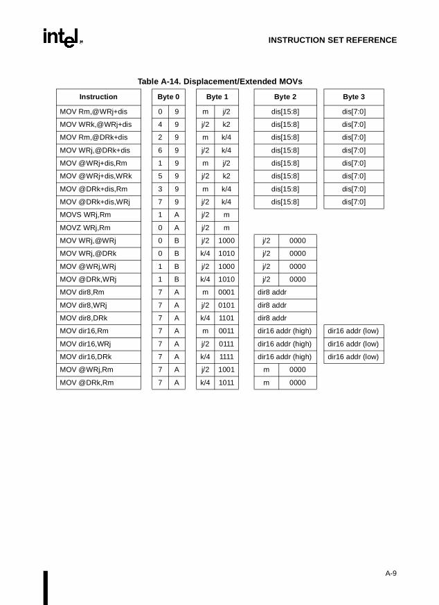
INSTRUCTION SET REFERENCE
Table A-14. Displacement/Extended MOVs
Instruction Byte 0 Byte 1 Byte 2 Byte 3
MOV Rm,@WRj+dis 0 9 m j/2 dis[15:8] dis[7:0]
MOV WRk,@WRj+dis 4 9 j/2 k2 dis[15:8] dis[7:0]
MOV Rm,@DRk+dis 2 9 m k/4 dis[15:8] dis[7:0]
MOV WRj,@DRk+dis 6 9 j/2 k/4 dis[15:8] dis[7:0]
MOV @WRj+dis,Rm 1 9 m j/2 dis[15:8] dis[7:0]
MOV @WRj+dis,WRk 5 9 j/2 k2 dis[15:8] dis[7:0]
MOV @DRk+dis,Rm 3 9 m k/4 dis[15:8] dis[7:0]
MOV @DRk+dis,WRj 7 9 j/2 k/4 dis[15:8] dis[7:0]
MOVS WRj,Rm 1 A j/2 m
MOVZ WRj,Rm 0 A j/2 m
MOV WRj,@WRj 0 B j/2 1000 j/2 0000
MOV WRj,@DRk 0 B k/4 1010 j/2 0000
MOV @WRj,WRj 1 B j/2 1000 j/2 0000
MOV @DRk,WRj 1 B k/4 1010 j/2 0000
MOV dir8,Rm 7 A m 0001 dir8 addr
MOV dir8,WRj 7 A j/2 0101 dir8 addr
MOV dir8,DRk 7 A k/4 1101 dir8 addr
MOV dir16,Rm 7 A m 0011 dir16 addr (high) dir16 addr (low)
MOV dir16,WRj 7 A j/2 0111 dir16 addr (high) dir16 addr (low)
MOV dir16,DRk 7 A k/4 1111 dir16 addr (high) dir16 addr (low)
MOV @WRj,Rm 7 A j/2 1001 m 0000
MOV @DRk,Rm 7 A k/4 1011 m 0000
A-9

8x930Ax, 8x930Hx USER’S MANUAL
Table A-15. INC/DEC
Instruction Byte 0 Byte 1
1 INC Rm,#short 0 B m 00 ss
2 INC WRj,#short 0 B j/2 01 ss
3 INC DRk,#short 0 B k/4 11 ss
4 DEC Rm,#short 1 B m 00 ss
5 DEC WRj,#short 1 B j/2 01 ss
6 DEC DRk,#short 1 B k/4 11 ss
Table A-16. Encoding for INC/DEC
ss #short
00 1
01 2
10 4
Table A-17. Shifts
Instruction Byte 0 Byte 1
1 SRA Rm 0 E m 0000
2 SRA WRj 0 E j/2 0100
3 SRL Rm 1 E m 0000
4 SRL WRj 1 E j/2 0100
5 SLL Rm 3 E m 0000
6 SLL WRj 3 E j/2 0100
A-10

INSTRUCTION SET REFERENCE
re is a
t
E, and
_TIME.
A.3 INSTRUCTION SET SUMMARY
This section contains tables that summarize the instruction set. For each instruction theshort description, its length in bytes, and its execution time in states.
NOTEExecution times are increased by executing code from external memory, accessing peripheral SFRs, accessing data in external memory, using a wait state, or extending the ALE pulse.
For some instructions, accessing the port SFRs, Px, x = 0–3, increases the execution time. These cases are noted individually in the tables.
A.3.1 Execution Times for Instructions Accessing the Port SFRs
Table A-18 lists these instructions and the execution times.
• Case 1. Code executes from external memory with no wait state and a short ALE (notextended) and accesses a port SFR.
• Case 2. Code executes from external memory with one wait state and a short ALE (noextended) and accesses a port SFR.
• Case 3. Code executes from external memory with one wait state and an extended ALaccesses a port SFR.
Times for each case are expressed as the number of state times to be added to the BASE
Table A-18. State Times to Access the Port SFRs
InstructionBASE_TIME Additional State Times
(Add to the BASE_TIME column)
Binary Source Case 1 Case 2 Case 3
ADD A,dir8 1 1 2 3 4
ADD Rm,dir8 3 2 2 3 4
ADDC A,dir8 1 1 2 3 4
ANL A,dir8 1 1 2 3 4
ANL CY,bit 3 2 2 3 4
ANL CY,bit51 1 1 2 3 4
ANL CY,/bit 3 2 2 3 4
ANL CY,/bit51 1 1 2 3 4
ANL dir8,#data 3 3 4 6 8
ANL dir8,A 2 2 4 6 8
ANL Rm,dir8 3 2 2 3 4
CLR bit 4 3 4 6 8
CLR bit51 2 2 4 6 8
A-11

8x930Ax, 8x930Hx USER’S MANUAL
CMP Rm,dir8 3 2 2 3 4
CPL bit 4 3 4 6 8
CPL bit51 2 2 4 6 8
DEC dir8 2 2 4 6 8
INC dir8 2 2 4 6 8
MOV A,dir8 1 1 2 3 4
MOV bit,CY 4 3 4 6 8
MOV bit51,CY 2 2 4 6 8
MOV CY,bit 3 2 2 3 4
MOV CY,bit51 1 1 2 3 4
MOV dir8,#data 3 3 2 3 4
MOV dir8,A 2 2 2 3 4
MOV dir8,Rm 4 3 2 3 4
MOV dir8,Rn 2 3 2 3 4
MOV Rm,dir8 3 2 2 3 4
MOV Rn,dir8 1 2 2 3 4
ORL A,dir8 1 1 2 3 4
ORL CY,bit 3 2 2 3 4
ORL CY,bit51 1 1 2 3 4
ORL CY,/bit 3 2 2 3 4
ORL CY,/bit51 1 1 2 3 4
ORL dir8,#data 3 3 2 3 4
ORL dir8,A 2 2 4 6 8
ORL Rm,dir8 3 2 2 3 4
SETB bit 4 3 4 6 8
SETB bit51 2 2 4 6 8
SUB Rm,dir8 3 2 2 3 4
SUBB A,dir8 1 1 2 3 4
XCH A,dir8 3 3 4 6 8
XRL A,dir8 1 1 2 3 4
XRL dir8,#data 3 3 4 6 8
XRL dir8,A 2 2 4 6 8
XRL Rm,dir8 3 2 2 3 4
Table A-18. State Times to Access the Port SFRs (Continued)
InstructionBASE_TIME Additional State Times
(Add to the BASE_TIME column)
Binary Source Case 1 Case 2 Case 3
A-12
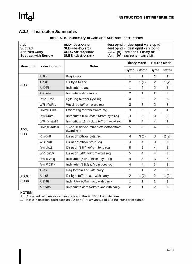
INSTRUCTION SET REFERENCE
A.3.2 Instruction Summaries
Table A-19. Summary of Add and Subtract Instructions
Add ADD <dest>,<src> dest opnd ← dest opnd + src opndSubtract SUB <dest>,<src> dest opnd ← dest opnd - src opndAdd with Carry ADDC <dest>,<src> (A) ← (A) + src opnd + carry bitSubtract with Borrow SUBB <dest>,<src> (A) ← (A) - src opnd - carry bit
Mnemonic <dest>,<src> NotesBinary Mode Source Mode
Bytes States Bytes States
ADD
A,Rn Reg to acc 1 1 2 2
A,dir8 Dir byte to acc 2 1 (2) 2 1 (2)
A,@Ri Indir addr to acc 1 2 2 3
A,#data Immediate data to acc 2 1 2 1
ADD;
SUB
Rmd,Rms Byte reg to/from byte reg 3 2 2 1
WRjd,WRjs Word reg to/from word reg 3 3 2 2
DRkd,DRks Dword reg to/from dword reg 3 5 2 4
Rm,#data Immediate 8-bit data to/from byte reg 4 3 3 2
WRj,#data16 Immediate 16-bit data to/from word reg 5 4 4 3
DRk,#0data16 16-bit unsigned immediate data to/from dword reg
5 6 4 5
Rm,dir8 Dir addr to/from byte reg 4 3 (2) 3 2 (2)
WRj,dir8 Dir addr to/from word reg 4 4 3 3
Rm,dir16 Dir addr (64K) to/from byte reg 5 3 4 2
WRj,dir16 Dir addr (64K) to/from word reg 5 4 4 3
Rm,@WRj Indir addr (64K) to/from byte reg 4 3 3 2
Rm,@DRk Indir addr (16M) to/from byte reg 4 4 3 3
ADDC;
SUBB
A,Rn Reg to/from acc with carry 1 1 2 2
A,dir8 Dir byte to/from acc with carry 2 1 (2) 2 1 (2)
A,@Ri Indir RAM to/from acc with carry 1 2 2 3
A,#data Immediate data to/from acc with carry 2 1 2 1
NOTES:1. A shaded cell denotes an instruction in the MCS® 51 architecture.2. If this instruction addresses an I/O port (Px, x = 3:0), add 1 to the number of states.
A-13

8x930Ax, 8x930Hx USER’S MANUAL
Table A-20. Summary of Compare Instructions
Compare CMP <dest>,<src> dest opnd – src opnd
Mnemonic <dest>,<src> NotesBinary Mode Source Mode
Bytes States Bytes States
CMP
Rmd,Rms Reg with reg 3 2 2 1
WRjd,WRjs Word reg with word reg 3 3 2 2
DRkd,DRks Dword reg with dword reg 3 5 2 4
Rm,#data Reg with immediate data 4 3 3 2
WRj,#data16 Word reg with immediate 16-bit data 5 4 4 3
DRk,#0data16 Dword reg with zero-extended 16-bit immediate data
5 6 4 5
DRk,#1data16 Dword reg with one-extended 16-bit immediate data
5 6 4 5
Rm,dir8 Dir addr from byte reg 4 3† 3 2†
WRj,dir8 Dir addr from word reg 4 4 3 3
Rm,dir16 Dir addr (64K) from byte reg 5 3 4 2
WRj,dir16 Dir addr (64K) from word reg 5 4 4 3
Rm,@WRj Indir addr (64K) from byte reg 4 3 3 2
Rm,@DRk Indir addr (16M) from byte reg 4 4 3 3
† If this instruction addresses an I/O port (Px, x = 3:0), add 1 to the number of states.
Table A-21. Summary of Increment and Decrement Instructions
Increment INC DPTR (DPTR) ← (DPTR) + 1Increment INC byte byte ← byte + 1Increment INC <dest>,<src> dest opnd ← dest opnd + src opndDecrement DEC byte byte ← byte – 1Decrement DEC <dest>,<src> dest opnd ← dest opnd - src opnd
Mnemonic <dest>,<src> NotesBinary Mode Source Mode
Bytes States Bytes States
INC;
DEC
A acc 1 1 1 1
Rn Reg 1 1 2 2
dir8 Dir byte 2 2 (2) 2 2 (2)
@Ri Indir RAM 1 3 2 4
Rm,#short Byte reg by 1, 2, or 4 3 2 2 1
WRj,#short Word reg by 1, 2, or 4 3 2 2 1
DRk,#short Double word reg by 1, 2, or 4 3 4 2 3
NOTES:1. A shaded cell denotes an instruction in the MCS® 51 architecture.2. If this instruction addresses an I/O port (Px, x = 0–3), add 2 to the number of states.
A-14

INSTRUCTION SET REFERENCE
INC DPTR Data pointer 1 1 1 1
Table A-22. Summary of Multiply, Divide, and Decimal-adjust Instruct ions
Multiply MUL <reg1,reg2> (2)MUL AB (B:A) = A x B
Divide DIV <reg1>,<reg2> (2)DIV AB (A) = Quotient; (B) =Remainder
Decimal-adjust ACC DA A (2)for Addition (BCD)
Mnemonic <dest>,<src> NotesBinary Mode Source Mode
Bytes States Bytes States
MUL
AB Multiply A and B 1 5 1 5
Rmd,Rms Multiply byte reg and byte reg 3 6 2 5
WRjd,WRjs Multiply word reg and word reg 3 12 2 11
DIV
AB Divide A by B 1 10 1 10
Rmd,Rms Divide byte reg by byte reg 3 11 2 10
WRjd,WRjs Divide word reg by word reg 3 21 2 20
DA A Decimal adjust acc 1 1 1 1
NOTES:1. A shaded cell denotes an instruction in the MCS® 51 architecture.2. See “Instruction Descriptions” on page A-25.
Table A-21. Summary of Increment and Decrement Instructions (Continued)
Increment INC DPTR (DPTR) ← (DPTR) + 1Increment INC byte byte ← byte + 1Increment INC <dest>,<src> dest opnd ← dest opnd + src opndDecrement DEC byte byte ← byte – 1Decrement DEC <dest>,<src> dest opnd ← dest opnd - src opnd
Mnemonic <dest>,<src> NotesBinary Mode Source Mode
Bytes States Bytes States
NOTES:1. A shaded cell denotes an instruction in the MCS® 51 architecture.2. If this instruction addresses an I/O port (Px, x = 0–3), add 2 to the number of states.
A-15

8x930Ax, 8x930Hx USER’S MANUAL
Table A-23. Summary of Logical Instructions
Logical AND ANL <dest>,<src> dest opnd ←dest opnd Λ src opndLogical OR ORL <dest>,<src> dest opnd ← dest opnd V src opndLogical Exclusive OR XRL <dest>,<src> dest opnd ← dest opnd ∀ src opndClear CLR A (A) ← 0Complement CPL A (Ai) ← Ø(Ai) Rotate RXX A (1) Shift SXX Rm or Wj (1) SWAP A A3:0 ↔ A7:4
Mnemonic <dest>,<src> NotesBinary Mode Source Mode
Bytes States Bytes States
ANL;
ORL;
XRL;
A,Rn Reg to acc 1 1 2 2
A,dir8 Dir byte to acc 2 1 (3) 2 1 (3)
A,@Ri Indir addr to acc 1 2 2 3
A,#data Immediate data to acc 2 1 2 1
dir8,A Acc to dir byte 2 2 (4) 2 2 (4)
dir8,#data Immediate data to dir byte 3 3 (4) 3 3 (4)
Rmd,Rms Byte reg to byte reg 3 2 2 1
WRjd,WRjs Word reg to word reg 3 3 2 2
Rm,#data 8-bit data to byte reg 4 3 3 2
WRj,#data16 16-bit data to word reg 5 4 4 3
Rm,dir8 Dir addr to byte reg 4 3 (3) 3 2 (3)
WRj,dir8 Dir addr to word reg 4 4 3 3
Rm,dir16 Dir addr (64K) to byte reg 5 3 4 2
WRj,dir16 Dir addr (64K) to word reg 5 4 4 3
Rm,@WRj Indir addr (64K) to byte reg 4 3 3 2
Rm,@DRk Indir addr (16M) to byte reg 4 4 3 3
CLR A Clear acc 1 1 1 1
CPL A Complement acc 1 1 1 1
RL A Rotate acc left 1 1 1 1
RLC A Rotate acc left through the carry 1 1 1 1
RR A Rotate acc right 1 1 1 1
RRC A Rotate acc right through the carry 1 1 1 1
SLLRm Shift byte reg left 3 2 2 1
WRj Shift word reg left 3 2 2 1
NOTES:1. See “Instruction Descriptions” on page A-25.2. A shaded cell denotes an instruction in the MCS® 51 architecture.3. If this instruction addresses an I/O port (Px, x = 0–3), add 1 to the number of states.4. If this instruction addresses an I/O port (Px, x = 0–3), add 2 to the number of states.
A-16

INSTRUCTION SET REFERENCE
SRARm Shift byte reg right through the MSB 3 2 2 1
WRj Shift word reg right through the MSB 3 2 2 1
SRLRm Shift byte reg right 3 2 2 1
WRj Shift word reg right 3 2 2 1
SWAP A Swap nibbles within the acc 1 2 1 2
Table A-23. Summary of Logical Instructions (Continued)
Logical AND ANL <dest>,<src> dest opnd ←dest opnd Λ src opndLogical OR ORL <dest>,<src> dest opnd ← dest opnd V src opndLogical Exclusive OR XRL <dest>,<src> dest opnd ← dest opnd ∀ src opndClear CLR A (A) ← 0Complement CPL A (Ai) ← Ø(Ai) Rotate RXX A (1) Shift SXX Rm or Wj (1) SWAP A A3:0 ↔ A7:4
Mnemonic <dest>,<src> NotesBinary Mode Source Mode
Bytes States Bytes States
NOTES:1. See “Instruction Descriptions” on page A-25.2. A shaded cell denotes an instruction in the MCS® 51 architecture.3. If this instruction addresses an I/O port (Px, x = 0–3), add 1 to the number of states.4. If this instruction addresses an I/O port (Px, x = 0–3), add 2 to the number of states.
A-17

8x930Ax, 8x930Hx USER’S MANUAL
Table A-24. Summary of Move Instructions
Move (2) MOV <dest>,<src> destination ← src opndMove with Sign Extension MOVS <dest>,<src> destination ← src opnd with sign extendMove with Zero Extension MOVZ <dest>,<src> destination ← src opnd with zero extendMove Code Byte MOVC <dest>,<src> A ← code byteMove to External Mem MOVX <dest>,<src> external mem ← (A)Move from External Mem MOVX <dest>,<src> A ← source opnd in external mem
Mnemonic <dest>,<src> NotesBinary Mode Source Mode
Bytes States Bytes States
MOV
A,Rn Reg to acc 1 1 2 2
A,dir8 Dir byte to acc 2 1 (3) 2 1 (3)
A,@Ri Indir RAM to acc 1 2 2 3
A,#data Immediate data to acc 2 1 2 1
Rn,A Acc to reg 1 1 2 2
Rn,dir8 Dir byte to reg 2 1 (3) 3 2 (3)
Rn,#data Immediate data to reg 2 1 3 2
dir8,A Acc to dir byte 2 2 (3) 2 2 (3)
dir8,Rn Reg to dir byte 2 2 (3) 3 3 (3)
dir8,dir8 Dir byte to dir byte 3 3 3 3
dir8,@Ri Indir RAM to dir byte 2 3 3 4
dir8,#data Immediate data to dir byte 3 3 (3) 3 3 (3)
@Ri,A Acc to indir RAM 1 3 2 4
@Ri,dir8 Dir byte to indir RAM 2 3 3 4
@Ri,#data Immediate data to indir RAM 2 3 3 4
DPTR,#data16 Load Data Pointer with a 16-bit const 3 2 3 2
Rmd,Rms Byte reg to byte reg 3 2 2 1
WRjd,WRjs Word reg to word reg 3 2 2 1
DRkd,DRks Dword reg to dword reg 3 3 2 2
Rm,#data 8-bit immediate data to byte reg 4 3 3 2
WRj,#data16 16-bit immediate data to word reg 5 3 4 2
DRk,#0data16 zero-extended 16-bit immediate data to dword reg
5 5 4 4
DRk,#1data16 one-extended 16-bit immediate data to dword reg
5 5 4 4
NOTES:1. A shaded cell denotes an instruction in the MCS® 51 architecture.2. Instructions that move bits are in Table A-26.3. If this instruction addresses an I/O port (Px, x = 0–3), add 1 to the number of states.4. External memory addressed by instructions in the MCS 51 architecture is in the region specified by
DPXL (reset value = 01H). See “Compatibility with the MCS® 51 Architecture” on page 3-2.
A-18
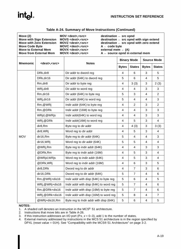
INSTRUCTION SET REFERENCE
MOV
DRk,dir8 Dir addr to dword reg 4 6 3 5
DRk,dir16 Dir addr (64K) to dword reg 5 6 4 5
Rm,dir8 Dir addr to byte reg 4 3 (3) 3 2 (3)
WRj,dir8 Dir addr to word reg 4 4 3 3
Rm,dir16 Dir addr (64K) to byte reg 5 3 4 2
WRj,dir16 Dir addr (64K) to word reg 5 4 4 3
Rm,@WRj Indir addr (64K) to byte reg 4 2 3 2
Rm,@DRk Indir addr (16M) to byte reg 4 4 3 3
WRjd,@WRjs Indir addr(64K) to word reg 4 4 3 3
WRj,@DRk Indir addr(16M) to word reg 4 5 3 4
dir8,Rm Byte reg to dir addr 4 4 (3) 3 3 (3)
dir8,WRj Word reg to dir addr 4 5 3 4
dir16,Rm Byte reg to dir addr (64K) 5 4 4 3
dir16,WRj Word reg to dir addr (64K) 5 5 4 4
@WRj,Rm Byte reg to indir addr (64K) 4 4 3 3
@DRk,Rm Byte reg to indir addr (16M) 4 5 3 4
@WRjd,WRjs Word reg to indir addr (64K) 4 5 3 4
@DRk,WRj Word reg to indir addr (16M) 4 6 3 5
dir8,DRk Dword reg to dir addr 4 7 3 6
dir16,DRk Dword reg to dir addr (64K) 5 7 4 6
Rm,@WRj+dis16 Indir addr with disp (64K) to byte reg 5 6 4 5
WRj,@WRj+dis16 Indir addr with disp (64K) to word reg 5 7 4 6
Rm,@DRk+dis16 Indir addr with disp (16M) to byte reg 5 7 4 6
WRj,@DRk+dis16 Indir addr with disp (16M) to word reg 5 8 4 7
@WRj+dis16,Rm Byte reg to Indir addr with disp (64K) 5 6 4 5
Table A-24. Summary of Move Instructions (Continued)
Move (2) MOV <dest>,<src> destination ← src opndMove with Sign Extension MOVS <dest>,<src> destination ← src opnd with sign extendMove with Zero Extension MOVZ <dest>,<src> destination ← src opnd with zero extendMove Code Byte MOVC <dest>,<src> A ← code byteMove to External Mem MOVX <dest>,<src> external mem ← (A)Move from External Mem MOVX <dest>,<src> A ← source opnd in external mem
Mnemonic <dest>,<src> NotesBinary Mode Source Mode
Bytes States Bytes States
NOTES:1. A shaded cell denotes an instruction in the MCS® 51 architecture.2. Instructions that move bits are in Table A-26.3. If this instruction addresses an I/O port (Px, x = 0–3), add 1 to the number of states.4. External memory addressed by instructions in the MCS 51 architecture is in the region specified by
DPXL (reset value = 01H). See “Compatibility with the MCS® 51 Architecture” on page 3-2.
A-19

8x930Ax, 8x930Hx USER’S MANUAL
MOV
@WRj+dis16,WRj Word reg to Indir addr with disp (64K) 5 7 4 6
@DRk+dis16,Rm Byte reg to Indir addr with disp (16M) 5 7 4 6
@DRk+dis16,WRj Word reg to Indir addr with disp (16M)
5 8 4 7
MOVH DRk(hi), #data16 16-bit immediate data into upper word of dword reg
5 3 4 2
MOVS WRj,Rm Byte reg to word reg with sign extension
3 2 2 1
MOVZ WRj,Rm Byte reg to word reg with zeros extension
3 2 2 1
MOVCA,@A+DPTR Code byte relative to DPTR to acc 1 6 1 6
A,@A+PC Code byte relative to PC to acc 1 6 1 6
MOVX
A,@Ri External mem (8-bit addr) to acc (4) 1 4 2 5
A,@DPTR External mem (16-bit addr) to acc (4) 1 5 1 5
@Ri,A Acc to external mem (8-bit addr) (4) 1 4 1 4
@DPTR,A Acc to external mem (16-bit addr) (4) 1 5 1 5
Table A-24. Summary of Move Instructions (Continued)
Move (2) MOV <dest>,<src> destination ← src opndMove with Sign Extension MOVS <dest>,<src> destination ← src opnd with sign extendMove with Zero Extension MOVZ <dest>,<src> destination ← src opnd with zero extendMove Code Byte MOVC <dest>,<src> A ← code byteMove to External Mem MOVX <dest>,<src> external mem ← (A)Move from External Mem MOVX <dest>,<src> A ← source opnd in external mem
Mnemonic <dest>,<src> NotesBinary Mode Source Mode
Bytes States Bytes States
NOTES:1. A shaded cell denotes an instruction in the MCS® 51 architecture.2. Instructions that move bits are in Table A-26.3. If this instruction addresses an I/O port (Px, x = 0–3), add 1 to the number of states.4. External memory addressed by instructions in the MCS 51 architecture is in the region specified by
DPXL (reset value = 01H). See “Compatibility with the MCS® 51 Architecture” on page 3-2.
A-20

INSTRUCTION SET REFERENCE
Table A-25. Summary of Exchange, Push, and Pop Instructions
Exchange Contents XCH <dest>,<src> A ↔ src opndExchange Digit XCHD <dest>,<src> A3:0 ↔ on-chip RAM bits 3:0Push PUSH <src> SP ← SP + 1; (SP) ← src Pop POP <dest> dest ← (SP); SP ← SP – 1
Mnemonic <dest>,<src> NotesBinary Mode Source Mode
Bytes States Bytes States
XCH
A,Rn Acc and reg 1 3 2 4
A,dir8 Acc and dir addr 2 3 (2) 2 3 (2)
A,@Ri Acc and on-chip RAM (8-bit addr) 1 4 2 5
XCHD A,@Ri Acc and low nibble in on-chip RAM (8-bit addr)
1 4 2 5
PUSH
dir8 Push dir byte onto stack 2 2 2 2
#data Push immediate data onto stack 4 4 3 3
#data16 Push 16-bit immediate data onto stack
5 5 4 5
Rm Push byte reg onto stack 3 4 2 3
WRj Push word reg onto stack 3 6 2 5
DRk Push double word reg onto stack 3 10 2 9
POP
Dir Pop dir byte from stack 2 3/3 2 3/3
Rm Pop byte reg from stack 3 3 2 2
WRj Pop word reg from stack 3 5 2 4
DRk Pop double word reg from stack 3 9 2 8
NOTES:1. A shaded cell denotes an instruction in the MCS® 51 architecture.2. If this instruction addresses an I/O port (Px, x = 0–3), add 2 to the number of states.
A-21

8x930Ax, 8x930Hx USER’S MANUAL
Table A-26. Summary of Bit Instructions
Clear Bit CLR bit bit ← 0Set Bit SETB bit bit ← 1Complement Bit CPL bit bit ← ØbitAND Carry with Bit ANL CY,bit CY ← CY Λ bitAND Carry with Complement of Bit ANL CY,/bit CY ← CY Λ ØbitOR Carry with Bit ORL CY,bit CY ← CY V bitORL Carry with Complement of Bit ORL CY,/bit CY ← CY V ØbitMove Bit to Carry MOV CY,bit CY ← bit Move Bit from Carry MOV bit,CY bit ← CY
Mnemonic <src>,<dest> NotesBinary Mode Source Mode
Bytes States Bytes States
CLR
CY Clear carry 1 1 1 1
bit51 Clear dir bit 2 2 (2) 2 2 (2)
bit Clear dir bit 4 4 3 3
SETB
CY Set carry 1 1 1 1
bit51 Set dir bit 2 2 (2) 2 2 (2)
bit Set dir bit 4 4 (2) 3 3 (2)
CPL
CY Complement carry 1 1 1 1
bit51 Complement dir bit 2 2 (2) 2 2 (2)
bit Complement dir bit 4 4 (2) 3 3 (2)
ANLCY,bit51 AND dir bit to carry 2 1 (3) 2 1 (3)
CY,bit AND dir bit to carry 4 3 (3) 3 2 (3)
ANL/CY,/bit51 AND complemented dir bit to carry 2 1 (3) 2 1 (3)
CY,/bit AND complemented dir bit to carry 4 3 (3) 3 2 (3)
ORLCY,bit51 OR dir bit to carry 2 1 (3) 2 1 (3)
CY,bit OR dir bit to carry 4 3 (3) 3 2 (3)
ORL/CY,/bit51 OR complemented dir bit to carry 2 1 (3) 2 1 (3)
CY,/bit OR complemented dir bit to carry 4 3 (3) 3 2 (3)
MOV
CY,bit51 Move dir bit to carry 2 1 (3) 2 1 (3)
CY,bit Move dir bit to carry 4 3 (3) 3 2 (3)
bit51,CY Move carry to dir bit 2 2 (2) 2 2 (2)
bit,CY Move carry to dir bit 4 4 (2) 3 3 (2)
NOTES:1. A shaded cell denotes an instruction in the MCS® 51 architecture.2. If this instruction addresses an I/O port (Px, x = 0–3), add 2 to the number of states.3. If this instruction addresses an I/O port (Px, x = 0–3), add 1 to the number of states.
A-22

INSTRUCTION SET REFERENCE
Table A-27. Summary of Control Instructions
Mnemonic <dest>,<src> NotesBinary Mode Source Mode
Bytes States (2) Bytes States (2)
ACALL addr11 Absolute subroutine call 2 9 2 9
ECALL@DRk Extended subroutine call, indirect 3 12 2 11
addr24 Extended subroutine call 5 14 4 13
LCALL@WRj Long subroutine call, indirect 3 9 2 8
addr16 Long subroutine call 3 9 3 9
RET Return from subroutine 1 6 1 6
ERET Extended subroutine return 3 10 2 9
RETI Return from interrupt 1 6 1 6
AJMP addr11 Absolute jump 2 3 2 3
EJMPaddr24 Extended jump 5 6 4 5
@DRk Extended jump, indirect 3 7 2 6
LJMP@WRj Long jump, indirect 3 6 2 5
addr16 Long jump 3 4 3 4
SJMP rel Short jump (relative addr) 2 3 2 3
JMP @A+DPTR Jump indir relative to the DPTR 1 5 1 5
JC rel Jump if carry is set 2 1/4 2 1/4
JNC rel Jump if carry not set 2 1/4 2 1/4
JB
bit51,rel Jump if dir bit is set 3 2/5 3 2/5
bit,rel Jump if dir bit of 8-bit addr location is set
5 4/7 4 3/6
JNB
bit51,rel Jump if dir bit is not set 3 2/5 3 2/5
bit,rel Jump if dir bit of 8-bit addr location is not set
5 4/7 4 3/6
JBC
bit51,rel Jump if dir bit is set & clear bit 3 4/7 3 4/7
bit,rel Jump if dir bit of 8-bit addr location is set and clear bit
5 7/10 4 6/9
JZ rel Jump if acc is zero 2 2/5 2 2/5
JNZ rel Jump if acc is not zero 2 2/5 2 2/5
JE rel Jump if equal 3 2/5 2 1/4
JNE rel Jump if not equal 3 2/5 2 1/4
JG rel Jump if greater than 3 2/5 2 1/4
JLE rel Jump if less than or equal 3 2/5 2 1/4
JSL rel Jump if less than (signed) 3 2/5 2 1/4
NOTES:1. A shaded cell denotes an instruction in the MCS® 51 architecture.2. For conditional jumps, times are given as not-taken/taken.
A-23

8x930Ax, 8x930Hx USER’S MANUAL
JSLE rel Jump if less than or equal (signed) 3 2/5 2 1/4
JSG rel Jump if greater than (signed) 3 2/5 2 1/4
JSGE rel Jump if greater than or equal (signed)
3 2/5 2 1/4
CJNE
A,dir8,rel Compare dir byte to acc and jump if not equal
3 2/5 3 2/5
A,#data,rel Compare immediate to acc and jump if not equal
3 2/5 3 2/5
Rn,#data,rel Compare immediate to reg and jump if not equal
3 2/5 4 3/6
@Ri,#data,rel Compare immediate to indir and jump if not equal
3 3/6 4 4/7
DJNZ
Rn,rel Decrement reg and jump if not zero
2 2/5 3 3/6
dir8,rel Decrement dir byte and jump if not zero
3 3/6 3 3/6
TRAP — Jump to the trap interrupt vector 2 10 1 9
NOP — No operation 1 1 1 1
Table A-27. Summary of Control Instructions (Continued)
Mnemonic <dest>,<src> NotesBinary Mode Source Mode
Bytes States (2) Bytes States (2)
NOTES:1. A shaded cell denotes an instruction in the MCS® 51 architecture.2. For conditional jumps, times are given as not-taken/taken.
A-24
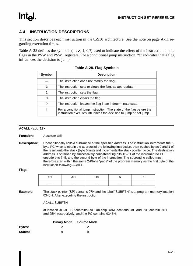
INSTRUCTION SET REFERENCE
re-
the flag
A.4 INSTRUCTION DESCRIPTIONS
This section describes each instruction in the 8x930 architecture. See the note on page A-11 garding execution times.
Table A-28 defines the symbols (—, , 1, 0,?) used to indicate the effect of the instruction on flags in the PSW and PSW1 registers. For a conditional jump instruction, “!” indicates that ainfluences the decision to jump.
ACALL <addr11>
Function: Absolute call
Description: Unconditionally calls a subroutine at the specified address. The instruction increments the 3-byte PC twice to obtain the address of the following instruction, then pushes bytes 0 and 1 of the result onto the stack (byte 0 first) and increments the stack pointer twice. The destination address is obtained by successively concatenating bits 15–11 of the incremented PC, opcode bits 7–5, and the second byte of the instruction. The subroutine called must therefore start within the same 2-Kbyte “page” of the program memory as the first byte of the instruction following ACALL.
Flags:
Example: The stack pointer (SP) contains 07H and the label "SUBRTN" is at program memory location 0345H. After executing the instruction
ACALL SUBRTN
at location 0123H, SP contains 09H; on-chip RAM locations 08H and 09H contain 01H and 25H, respectively; and the PC contains 0345H.
Binary Mode Source Mode
Bytes: 2 2
States: 9 9
Table A-28. Flag Symbols
Symbol Description
— The instruction does not modify the flag.
3 The instruction sets or clears the flag, as appropriate.
1 The instruction sets the flag.
0 The instruction clears the flag.
? The instruction leaves the flag in an indeterminate state.
! For a conditional jump instruction: The state of the flag before the instruction executes influences the decision to jump or not jump.
CY AC OV N Z
— — — — —
A-25

8x930Ax, 8x930Hx USER’S MANUAL
Hex Code in: Binary Mode = [Encoding]Source Mode = [Encoding]
Operation: ACALL (PC) ← (PC) + 2 (SP) ← (SP) + 1 ((SP)) ← (PC.7:0)(SP) ← (SP) + 1 ((SP)) ← (PC.15:8) (PC.10:0) ← page address
ADD <dest>,<src>
Function: Add
Description: Adds the source operand to the destination operand, which can be a register or the accumu-lator, leaving the result in the register or accumulator. If there is a carry out of bit 7 (CY), the CY flag is set. If byte variables are added, and if there is a carry out of bit 3 (AC), the AC flag is set. For addition of unsigned integers, the CY flag indicates that an overflow occurred.
If there is a carry out of bit 6 but not out of bit 7, or a carry out of bit 7 but not bit 6, the OV flag is set. When adding signed integers, the OV flag indicates a negative number produced as the sum of two positive operands, or a positive sum from two negative operands.
Bit 6 and bit 7 in this description refer to the most significant byte of the operand (8, 16, or 32 bit).
Four source operand addressing modes are allowed: register, direct, register-indirect, and immediate.
Flags:
Example: Register 1 contains 0C3H (11000011B) and register 0 contains 0AAH (10101010B). After executing the instruction
ADD R1,R0
register 1 contains 6DH (01101101B), the AC flag is clear, and the CY and OV flags are set.
Variations
ADD A,#data
Binary Mode Source Mode
Bytes: 2 2
States: 1 1
[Encoding] a10 a9 a8 1 0 0 0 1 a7 a6 a5 a4 a3 a2 a1 a0
CY AC OV N Z
3 3 3 3 3
[Encoding] 0 0 1 0 0 1 0 0 immed. data
A-26
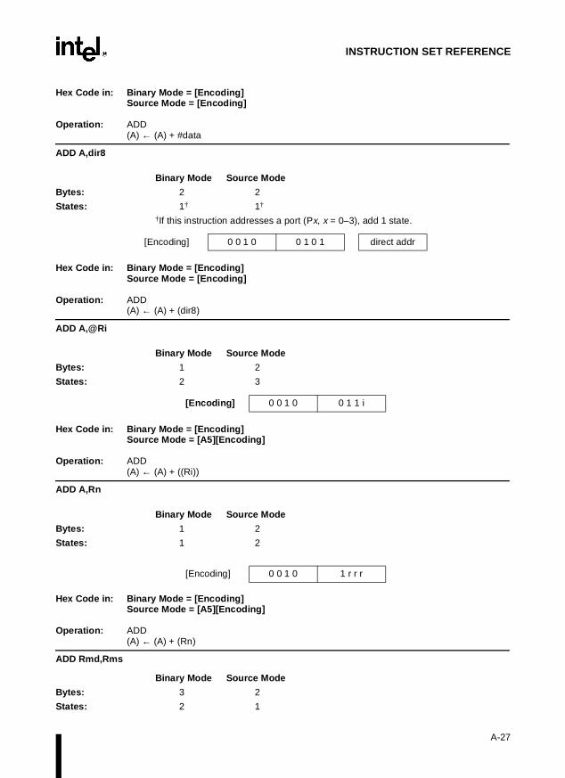
INSTRUCTION SET REFERENCE
Hex Code in: Binary Mode = [Encoding]Source Mode = [Encoding]
Operation: ADD (A) ← (A) + #data
ADD A,dir8
Binary Mode Source Mode
Bytes: 2 2
States: 1† 1†
†If this instruction addresses a port (Px, x = 0–3), add 1 state.
Hex Code in: Binary Mode = [Encoding]Source Mode = [Encoding]
Operation: ADD (A) ← (A) + (dir8)
ADD A,@Ri
Binary Mode Source Mode
Bytes: 1 2
States: 2 3
Hex Code in: Binary Mode = [Encoding]Source Mode = [A5][Encoding]
Operation: ADD (A) ← (A) + ((Ri))
ADD A,Rn
Binary Mode Source Mode
Bytes: 1 2
States: 1 2
Hex Code in: Binary Mode = [Encoding]Source Mode = [A5][Encoding]
Operation: ADD (A) ← (A) + (Rn)
ADD Rmd,Rms
Binary Mode Source Mode
Bytes: 3 2
States: 2 1
[Encoding] 0 0 1 0 0 1 0 1 direct addr
[Encoding] 0 0 1 0 0 1 1 i
[Encoding] 0 0 1 0 1 r r r
A-27

8x930Ax, 8x930Hx USER’S MANUAL
Hex Code in: Binary Mode = [A5][Encoding]Source Mode = [Encoding]
Operation: ADD (Rmd) ← (Rmd) + (Rms)
ADD WRjd,WRjs
Binary Mode Source Mode
Bytes: 3 2
States: 3 2
Hex Code in: Binary Mode = [A5][Encoding]Source Mode = [Encoding]
Operation: ADD (WRjd) ← (WRjd) + (WRjs)
ADD DRkd,DRks
Binary Mode Source Mode
Bytes: 3 2
States: 5 4
Hex Code in: Binary Mode = [A5][Encoding]Source Mode = [Encoding]
Operation: ADD (DRkd) ← (DRkd) + (DRks)
ADD Rm,#data
Binary Mode Source Mode
Bytes: 4 3
States: 3 2
Hex Code in: Binary Mode = [A5][Encoding]Source Mode = [Encoding]
Operation: ADD (Rm) ← (Rm) + #data
[Encoding] 0 0 1 0 1 1 0 0 s s s s S S S S
[Encoding] 0 0 1 0 1 1 0 1 t t t t T T T T
[Encoding] 0 0 1 0 1 1 1 1 u u u u U U U U
[Encoding] 0 0 1 0 1 1 1 0 s s s s 0 0 0 0 #data
A-28

INSTRUCTION SET REFERENCE
ADD WRj,#data16
Binary Mode Source Mode
Bytes: 5 4
States: 4 3
[Encoding]
Hex Code in: Binary Mode = [A5][Encoding]Source Mode = [Encoding]
Operation: ADD (WRj) ← (WRj) + #data16
ADD DRk,#0data16
Binary Mode Source Mode
Bytes: 5 4
States: 6 5
[Encoding]
Hex Code in: Binary Mode = [A5][Encoding]Source Mode = [Encoding]
Operation: ADD (DRk) ← (DRk) + #data16
ADD Rm,dir8
Binary Mode Source Mode
Bytes: 4 3
States: 3† 2†
†If this instruction addresses a port (Px, x = 0–3), add 1 state.
Hex Code in: Binary Mode = [A5][Encoding]Source Mode = [Encoding]
Operation: ADD (Rm) ← (Rm) + (dir8)
ADD WRj,dir8
Binary Mode Source Mode
Bytes: 4 3
States: 4 3
0 0 1 0 1 1 1 0 t t t t 0 1 0 0 #data hi #data low
0 0 1 0 1 1 1 0 u u u u 1 0 0 0 #data hi #data low
[Encoding] 0 0 1 0 1 1 1 0 s s s s 0 0 0 1 direct addr
[Encoding] 0 0 1 0 1 1 1 0 t t t t 0 1 0 1 direct addr
A-29

8x930Ax, 8x930Hx USER’S MANUAL
Hex Code in: Binary Mode = [A5][Encoding]Source Mode = [Encoding
Operation: ADD (WRj) ← (WRj) + (dir8)
ADD Rm,dir16
Binary Mode Source Mode
Bytes: 5 4
States: 3 2
[Encoding]
Hex Code in: Binary Mode = [A5][Encoding]Source Mode = [Encoding]
Operation: ADD (Rm) ← (Rm) + (dir16)
ADD WRj,dir16
Binary Mode Source Mode
Bytes: 5 4
States: 4 3
[Encoding]
Hex Code in: Binary Mode = [A5][Encoding]Source Mode = [Encoding]
Operation: ADD (WRj) ← (WRj) + (dir16)
ADD Rm,@WRj
Binary Mode Source Mode
Bytes: 4 3
States: 3 2
[Encoding]
Hex Code in: Binary Mode = [A5][Encoding]Source Mode = [Encoding]
Operation: ADD (Rm) ← (Rm) + ((WRj))
0 0 1 0 1 1 1 0 s s s s 0 0 1 1 direct addr direct add
0 0 1 0 1 1 1 0 t t t t 0 1 1 1 direct addr direct addr
0 0 1 0 1 1 1 0 t t t t 1 0 0 1 s s s s 0 0 0 0
A-30
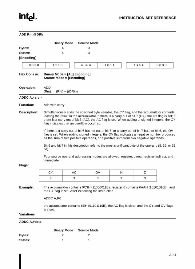
INSTRUCTION SET REFERENCE
ADD Rm,@DRk
Binary Mode Source Mode
Bytes: 4 3
States: 4 3
[Encoding]
Hex Code in: Binary Mode = [A5][Encoding]Source Mode = [Encoding]
Operation: ADD (Rm) ← (Rm) + ((DRk))
ADDC A,<src>
Function: Add with carry
Description: Simultaneously adds the specified byte variable, the CY flag, and the accumulator contents, leaving the result in the accumulator. If there is a carry out of bit 7 (CY), the CY flag is set; if there is a carry out of bit 3 (AC), the AC flag is set. When adding unsigned integers, the CY flag indicates that an overflow occurred.
If there is a carry out of bit 6 but not out of bit 7, or a carry out of bit 7 but not bit 6, the OV flag is set. When adding signed integers, the OV flag indicates a negative number produced as the sum of two positive operands, or a positive sum from two negative operands.
Bit 6 and bit 7 in this description refer to the most significant byte of the operand (8, 16, or 32 bit)
Four source operand addressing modes are allowed: register, direct, register-indirect, and immediate.
Flags:
Example: The accumulator contains 0C3H (11000011B), register 0 contains 0AAH (10101010B), and the CY flag is set. After executing the instruction
ADDC A,R0
the accumulator contains 6EH (01101110B), the AC flag is clear, and the CY and OV flags are set.
Variations
ADDC A,#data
Binary Mode Source Mode
Bytes: 2 2
States: 1 1
0 0 1 0 1 1 1 0 u u u u 1 0 1 1 s s s s 0 0 0 0
CY AC OV N Z
3 3 3 3 3
A-31

8x930Ax, 8x930Hx USER’S MANUAL
Hex Code in: Binary Mode = [Encoding]Source Mode = [Encoding]
Operation: ADDC (A) ← (A) + (CY) + #data
ADDC A,dir8
Binary Mode Source Mode
Bytes: 2 2
States: 1† 1†
†If this instruction addresses a port (Px, x = 0–3), add 1 state.
Hex Code in: Binary Mode = [Encoding]Source Mode = [Encoding]
Operation: ADDC (A) ← (A) + (CY) + (dir8)
ADDC A,@Ri
Binary Mode Source Mode
Bytes: 1 2
States: 2 3
Hex Code in: Binary Mode = [Encoding]Source Mode = [A5][Encoding]
Operation: ADDC (A) ← (A) + (CY) + ((Ri))
ADDC A,Rn
Binary Mode Source Mode
Bytes: 1 2
States: 1 2
Hex Code in: Binary Mode = [Encoding]Source Mode = [A5][Encoding]
Operation: ADDC (A) ← (A) + (CY) + (Rn)
[Encoding] 0 0 1 1 0 1 0 0 immed. data
[Encoding] 0 0 1 1 0 1 0 1 direct addr
[Encoding] 0 0 1 1 0 1 1 i
[Encoding] 0 0 1 1 1 r r r
A-32

INSTRUCTION SET REFERENCE
AJMP addr11
Function: Absolute jump
Description: Transfers program execution to the specified address, which is formed at run time by concat-enating the upper five bits of the PC (after incrementing the PC twice), opcode bits 7–5, and the second byte of the instruction. The destination must therefore be within the same 2-Kbyte “page” of program memory as the first byte of the instruction following AJMP.
Flags:
Example: The label "JMPADR" is at program memory location 0123H. After executing the instruction
AJMP JMPADR
at location 0345H, the PC contains 0123H.
Binary Mode Source Mode
Bytes: 2 2
States: 3 3
Hex Code in: Binary Mode = [Encoding]Source Mode = [Encoding]
Operation: AJMP (PC) ← (PC) + 2 (PC.10:0) ← page address
ANL <dest>,<src>
Function: Logical-AND
Description: Performs the bitwise logical-AND (Λ) operation between the specified variables and stores the results in the destination variable.
The two operands allow 10 addressing mode combinations. When the destination is the register or accumulator, the source can use register, direct, register-indirect, or immediate addressing; when the destination is a direct address, the source can be the accumulator or immediate data.
Note: When this instruction is used to modify an output port, the value used as the original port data is read from the output data latch, not the input pins.
Flags:
CY AC OV N Z
— — — — —
[Encoding] a10 a9 a8 0 0 0 0 1 a7 a6 a5 a4 a3 a2 a1 a0
CY AC OV N Z
— — — 3 3
A-33

8x930Ax, 8x930Hx USER’S MANUAL
Example: Register 1 contains 0C3H (11000011B) and register 0 contains 55H (01010101B). After executing the instruction
ANL R1,R0
register 1 contains 41H (01000001B).
When the destination is a directly addressed byte, this instruction clears combinations of bits in any RAM location or hardware register. The mask byte determining the pattern of bits to be cleared would either be an immediate constant contained in the instruction or a value computed in the register or accumulator at run time. The instruction
ANL P1,#01110011B
clears bits 7, 3, and 2 of output port 1.
Variations
ANL dir8,A
Binary Mode Source Mode
Bytes: 2 2
States: 2† 2†
†If this instruction addresses a port (Px, x = 0–3), add 2 states.
Hex Code in: Binary Mode = [Encoding]Source Mode = [Encoding]
Operation: ANL (dir8) ← (dir8) Λ (A)
ANL dir8,#data
Binary Mode Source Mode
Bytes: 3 3
States: 3† 3†
†If this instruction addresses a port (Px, x = 0–3), add 1 state.
Hex Code in: Binary Mode = [Encoding]Source Mode = [Encoding]
Operation: ANL (dir8) ← (dir8) Λ #data
ANL A,#data
Binary Mode Source Mode
Bytes: 2 2
States: 1 1
[Encoding] 0 1 0 1 0 0 1 0 direct addr
[Encoding] 0 1 0 1 0 0 1 1 direct addr immed. data
[Encoding] 0 1 0 1 0 1 0 0 immed. data
A-34

INSTRUCTION SET REFERENCE
Hex Code in: Binary Mode = [Encoding]Source Mode = [Encoding]
Operation: ANL (A) ← (A) Λ #data
ANL A,dir8
Binary Mode Source Mode
Bytes: 2 2
States: 1† 1†
†If this instruction addresses a port (Px, x = 0–3), add 1 state.
Hex Code in: Binary Mode = [Encoding]Source Mode = [Encoding]
Operation: ANL (A) ← (A) Λ (dir8)
ANL A,@Ri
Binary Mode Source Mode
Bytes: 1 2
States: 2 3
Hex Code in: Binary Mode = [Encoding]Source Mode = [A5][Encoding]
Operation: ANL (A) ← (A) Λ ((Ri))
ANL A,Rn
Binary Mode Source Mode
Bytes: 1 2
States: 1 2
Hex Code in: Binary Mode = [Encoding]Source Mode = [A5][Encoding]
Operation: ANL (A) ← (A) Λ (Rn)
ANL Rmd,Rms
Binary Mode Source Mode
Bytes: 3 2
States: 2 1
[Encoding] 0 1 0 1 0 1 0 1 direct addr
[Encoding] 0 1 0 1 0 1 1 i
[Encoding] 0 1 0 1 1 r r r
[Encoding] 0 1 0 1 1 1 0 0 s s s s S S S S
A-35

8x930Ax, 8x930Hx USER’S MANUAL
Hex Code in: Binary Mode = [A5][Encoding]Source Mode = [Encoding]
Operation: ANL (Rmd) ← (Rmd) Λ (Rms)
ANL WRjd,WRjs
Binary Mode Source Mode
Bytes: 3 2
States: 3 2
Hex Code in: Binary Mode = [A5][Encoding]Source Mode = [Encoding]
Operation: ANL (WRjd) ← (WRjd) Λ (WRjs)
ANL Rm,#data
Binary Mode Source Mode
Bytes: 4 3
States: 3 2
Hex Code in: Binary Mode = [A5][Encoding]Source Mode = [Encoding]
Operation: ANL (Rm) ← (Rm) Λ #data
ANL WRj,#data16
Binary Mode Source Mode
Bytes: 5 4
States: 4 3
[Encoding]
Hex Code in: Binary Mode = [A5][Encoding]Source Mode = [Encoding]
Operation: ANL (WRj) ← (WRj) Λ #data16
ANL Rm,dir8
Binary Mode Source Mode
Bytes: 4 3
States: 3† 2†
†If this instruction addresses a port (Px, x = 0–3), add 1 state.
[Encoding] 0 1 0 1 1 1 0 1 t t t t T T T T
[Encoding] 0 1 0 1 1 1 1 0 s s s s 0000 #data
0 1 0 1 1 1 1 0 t t t t 0 1 0 0 #data hi #data low
[Encoding] 0 1 0 1 1 1 1 0 s s s s 0 0 0 1 direct addr
A-36

INSTRUCTION SET REFERENCE
Hex Code in: Binary Mode = [A5][Encoding]Source Mode = [Encoding]
Operation: ANL (Rm) ← (Rm) Λ (dir8)
ANL WRj,dir8
Binary Mode Source Mode
Bytes: 4 3
States: 4 3
Hex Code in: Binary Mode = [A5][Encoding]Source Mode = [Encoding]
Operation: ANL (WRj) ← (WRj) Λ (dir8)
ANL Rm,dir16
Binary Mode Source Mode
Bytes: 5 4
States: 3 2
[Encoding]
Hex Code in: Binary Mode = [A5][Encoding]Source Mode = [Encoding]
Operation: ANL (Rm) ← (Rm) Λ (dir16)
ANL WRj,dir16
Binary Mode Source Mode
Bytes: 5 4
States: 4 3
[Encoding]
Hex Code in: Binary Mode = [A5][Encoding]Source Mode = [Encoding]
Operation: ANL (WRj) ← (WRj) Λ (dir16)
[Encoding] 0 1 0 1 1 1 10 t t t t 0 1 0 1 direct addr
0 1 0 1 1 1 1 0 s s s s 0 0 1 1 direct direct
0 1 0 1 1 1 1 0 t t t t 0 1 1 1 direct direct
A-37
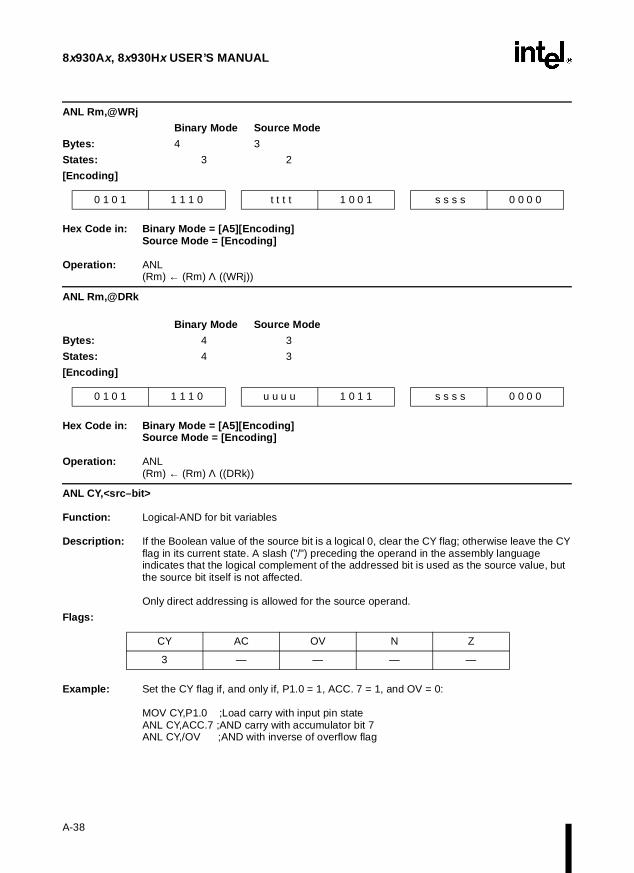
8x930Ax, 8x930Hx USER’S MANUAL
ANL Rm,@WRj
Binary Mode Source Mode
Bytes: 4 3
States: 3 2
[Encoding]
Hex Code in: Binary Mode = [A5][Encoding]Source Mode = [Encoding]
Operation: ANL (Rm) ← (Rm) Λ ((WRj))
ANL Rm,@DRk
Binary Mode Source Mode
Bytes: 4 3
States: 4 3
[Encoding]
Hex Code in: Binary Mode = [A5][Encoding]Source Mode = [Encoding]
Operation: ANL(Rm) ← (Rm) Λ ((DRk))
ANL CY,<src–bit>
Function: Logical-AND for bit variables
Description: If the Boolean value of the source bit is a logical 0, clear the CY flag; otherwise leave the CY flag in its current state. A slash ("/") preceding the operand in the assembly language indicates that the logical complement of the addressed bit is used as the source value, but the source bit itself is not affected.
Only direct addressing is allowed for the source operand.
Flags:
Example: Set the CY flag if, and only if, P1.0 = 1, ACC. 7 = 1, and OV = 0:
MOV CY,P1.0 ;Load carry with input pin stateANL CY,ACC.7 ;AND carry with accumulator bit 7 ANL CY,/OV ;AND with inverse of overflow flag
0 1 0 1 1 1 1 0 t t t t 1 0 0 1 s s s s 0 0 0 0
0 1 0 1 1 1 1 0 u u u u 1 0 1 1 s s s s 0 0 0 0
CY AC OV N Z
3 — — — —
A-38

INSTRUCTION SET REFERENCE
ANL CY,bit51
Binary Mode Source Mode
Bytes: 2 2
States: 1† 1†
†If this instruction addresses a port (Px, x = 0–3), add 1 state.
Hex Code in: Binary Mode = [Encoding]Source Mode = [Encoding]
Operation: ANL (CY) ← (CY) Λ (bit51)
ANL CY,/bit51
Binary Mode Source Mode
Bytes: 2 2
States: 1† 1†
†If this instruction addresses a port (Px, x = 0–3), add 1 state.
Hex Code in: Binary Mode = [Encoding]Source Mode = [Encoding]
Operation: ANL (CY) ← (CY) Λ Ø (bit51)
ANL CY,bit
Binary Mode Source Mode
Bytes: 4 3
States: 3† 2†
†If this instruction addresses a port (Px, x = 0–3), add 1 state.
[Encoding]
Hex Code in: Binary Mode = [A5][Encoding]Source Mode = [Encoding]
Operation: ANL (CY) ← (CY) Λ (bit)
ANL CY,/bit
Binary Mode Source Mode
Bytes: 4 3
States: 3† 2†
†If this instruction addresses a port (Px, x = 0–3), add 1 state.
[Encoding] 1 0 0 0 0 0 1 0 bit addr
[Encoding] 1 0 1 1 0 0 0 0 bit addr
1 0 1 0 1 0 0 1 1 0 0 0 0 y y y dir addr
A-39

8x930Ax, 8x930Hx USER’S MANUAL
[Encoding]
Hex Code in: Binary Mode = [A5][Encoding]Source Mode = [Encoding]
Operation: ANL (CY) ← (CY) Λ Ø (bit)
CJNE <dest>,<src>,rel
Function: Compare and jump if not equal. Description: Compares the magnitudes of the first two operands and branches if their values are not
equal. The branch destination is computed by adding the signed relative displacement in the last instruction byte to the PC, after incrementing the PC to the start of the next instruction. If the unsigned integer value of <dest-byte> is less than the unsigned integer value of <src-byte>, the CY flag is set. Neither operand is affected.
The first two operands allow four addressing mode combinations: the accumulator may be compared with any directly addressed byte or immediate data, and any indirect RAM location or working register can be compared with an immediate constant.
Flags:
Example: The accumulator contains 34H and R7 contains 56H. After executing the first instruction in the sequence
CJNE R7,#60H,NOT_EQ
; . . . . . . ;R7 = 60H
NOT_EQ: JC REQ_LOW ; IF R7 < 60H
; . . . . . . ;R7 > 60H
the CY flag is set and program execution continues at label NOT_EQ. By testing the CY flag, this instruction determines whether R7 is greater or less than 60H.
If the data being presented to Port 1 is also 34H, then executing the instruction,
WAIT: CJNE A,P1,WAIT
clears the CY flag and continues with the next instruction in the sequence, since the accumulator does equal the data read from P1. (If some other value was being input on P1, the program loops at this point until the P1 data changes to 34H.)
Variations
1 0 1 0 1 0 0 1 1 1 1 1 0 y y y dir addr
CY AC OV N Z
3 — — 3 3
A-40

INSTRUCTION SET REFERENCE
CJNE A,#data,rel
Binary Mode Source Mode
Not Taken Taken Not Taken Taken
Bytes: 3 3 3 3
States: 2 5 2 5
Hex Code in: Binary Mode = [Encoding]Source Mode = [Encoding]
Operation: (PC) ← (PC) + 3IF (A) ≠ #dataTHEN
(PC) ← (PC) + relative offsetIF (A) < #dataTHEN
(CY) ← 1ELSE
(CY) ← 0
CJNE A,dir8,rel
Binary Mode Source Mode
Not Taken Taken Not Taken Taken
Bytes: 3 3 3 3
States: 3 6 3 6
Hex Code in: Binary Mode = [Encoding]Source Mode = [Encoding]
Operation: (PC) ← (PC) + 3IF (A) ≠ dir8THEN
(PC) ← (PC) + relative offsetIF (A) < dir8THEN
(CY) ← 1ELSE
(CY) ← 0
[Encoding] 1 0 1 1 0 1 0 0 immed. data rel. addr
[Encoding] 1 0 1 1 0 1 0 1 direct addr rel. addr
A-41

8x930Ax, 8x930Hx USER’S MANUAL
CJNE @Ri,#data,rel
Binary Mode Source Mode
Not Taken Taken Not Taken Taken
Bytes: 3 3 4 4
States: 3 6 4 7
Hex Code in: Binary Mode = [Encoding]Source Mode = [A5][Encoding]
Operation: (PC) ← (PC) + 3IF ((Ri)) ≠ #dataTHEN
(PC) ← (PC) + relative offsetIF ((Ri)) < #dataTHEN
(CY) ← 1ELSE
(CY) ← 0
CJNE Rn,#data,rel
Binary Mode Source Mode
Not Taken Taken Not Taken Taken
Bytes: 3 3 4 4
States: 2 5 3 6
Hex Code in: Binary Mode = [Encoding]Source Mode = [A5][Encoding]
Operation: (PC) ← (PC) + 3IF (Rn) ≠ #dataTHEN
(PC) ← (PC) + relative offsetIF (Rn) < #dataTHEN
(CY) ← 1ELSE
(CY) ← 0
CLR A
Function: Clear accumulator
Description: Clears the accumulator (i.e., resets all bits to zero).
Flags:
[Encoding] 1 0 1 1 0 1 1 i immed. data rel. addr
[Encoding] 1 01 1 1 r r r immed. data rel. addr
CY AC OV N Z
— — — 3 3
A-42

INSTRUCTION SET REFERENCE
Example: The accumulator contains 5CH (01011100B). The instruction
CLR A
clears the accumulator to 00H (00000000B).
Binary Mode Source Mode
Bytes: 1 1
States: 1 1
Hex Code in: Binary Mode = [Encoding]Source Mode = [Encoding]
Operation: CLR (A) ← 0
CLR bit
Function: Clear bit
Description: Clears the specified bit. CLR can operate on the CY flag or any directly addressable bit.
Flags: Only for instructions with CY as the operand.
Example: Port 1 contains 5DH (01011101B). After executing the instruction
CLR P1.2
port 1 contains 59H (01011001B).
Variations
CLR bit51
Binary Mode Source Mode
Bytes: 4 3
States: 2† 2†
†If this instruction addresses a port (Px, x = 0–3), add 2 states.
Hex Code in: Binary Mode = [Encoding]Source Mode = [Encoding]
Operation: CLR (bit51) ← 0
[Encoding] 1 1 1 0 0 1 0 0
CY AC OV N Z
3 — — — —
[Encoding] 1 1 0 0 0 0 1 0 Bit addr
A-43

8x930Ax, 8x930Hx USER’S MANUAL
CLR CY
Binary Mode Source Mode
Bytes: 1 1
States: 1 1
Hex Code in: Binary Mode = [Encoding]Source Mode = [Encoding]
Operation: CLR (CY) ← 0
CLR bit
Binary Mode Source Mode
Bytes: 4 4
States: 4† 3†
†If this instruction addresses a port (Px, x = 0–3), add 2 states.
[Encoding]
Hex Code in: Binary Mode = [A5][Encoding]Source Mode = [Encoding]
Operation: CLR (bit) ← 0
CMP <dest>,<src>
Function: Compare
Description: Subtracts the source operand from the destination operand. The result is not stored in the destination operand. If a borrow is needed for bit 7, the CY (borrow) flag is set; otherwise it is clear.
When subtracting signed integers, the OV flag indicates a negative result when a negative value is subtracted from a positive value, or a positive result when a positive value is subtracted from a negative value.
Bit 7 in this description refers to the most significant byte of the operand (8, 16, or 32 bit)
The source operand allows four addressing modes: register, direct, immediate and indirect.
Flags:
[Encoding] 1 1 0 0 0 0 1 1
1 0 1 0 1 0 0 1 1 1 0 0 0 y y y dir addr
CY AC OV N Z
3 3 3 3 3
A-44

INSTRUCTION SET REFERENCE
Example: Register 1 contains 0C9H (11001001B) and register 0 contains 54H (01010100B). The instruction
CMP R1,R0
clears the CY and AC flags and sets the OV flag.
Variations
CMP Rmd,Rms
Binary Mode Source Mode
Bytes: 3 2
States: 2 1
Hex Code in: Binary Mode = [A5][Encoding]Source Mode = [Encoding]
Operation: CMP(Rmd) – (Rms)
CMP WRjd,WRjs
Binary Mode Source Mode
Bytes: 3 2
States: 3 2
Hex Code in: Binary Mode = [A5][Encoding]Source Mode = [Encoding]
Operation: CMP(WRjd) – (WRjs)
CMP DRkd,DRks
Binary Mode Source Mode
Bytes: 3 2
States: 5 4
Hex Code in: Binary Mode = [A5][Encoding]Source Mode = [Encoding]
Operation: CMP(DRkd) – (DRks)
[Encoding] 1 0 1 1 1 1 0 0 s s s s S S S S
[Encoding] 1 0 1 1 1 1 1 0 t t t t T T T T
[Encoding] 1 0 1 1 1 1 1 1 u u u u UUUU
A-45

8x930Ax, 8x930Hx USER’S MANUAL
CMP Rm,#data
Binary Mode Source Mode
Bytes: 4 3
States: 3 2
Hex Code in: Binary Mode = [A5][Encoding]Source Mode = [Encoding]
Operation: CMP (Rm) – #data
CMP WRj,#data16
Binary Mode Source Mode
Bytes: 5 4
States: 4 3
[Encoding]
Hex Code in: Binary Mode = [A5][Encoding]Source Mode = [Encoding]
Operation: CMP (WRj) – #data16
CMP DRk,#0data16
Binary Mode Source Mode
Bytes: 5 4
States: 6 5
[Encoding]
Hex Code in: Binary Mode = [A5][Encoding]Source Mode = [Encoding]
Operation: CMP (DRk) – #0data16
CMP DRk,#1data16
Binary Mode Source Mode
Bytes: 5 4
States: 6 5
[Encoding]
[Encoding] 1 0 1 1 1 1 1 0 s s s s 0 0 0 0 # data
1 0 1 1 1 1 1 0 t t t t 0 1 0 0 #data hi #data low
1 0 1 1 1 1 1 0 u u u u 1 0 0 0 #data hi #data low
1 0 1 1 1 1 1 0 u u u u 1 1 0 0 #data hi #data hi
A-46

INSTRUCTION SET REFERENCE
Hex Code in: Binary Mode = [A5][Encoding]Source Mode = [Encoding]
Operation: CMP (DRk) – #1data16
CMP Rm,dir8
Binary Mode Source Mode
Bytes: 4 3
States: 3† 2†
†If this instruction addresses a port (Px, x = 0–3), add 1 state.
Hex Code in: Binary Mode = [A5][Encoding]Source Mode = [Encoding]
Operation: CMP (Rm) – (dir8)
CMP WRj,dir8
Binary Mode Source Mode
Bytes: 4 3
States: 4 3
Hex Code in: Binary Mode = [A5][Encoding]Source Mode = [Encoding]
Operation: CMP (WRj) – (dir8)
CMP Rm,dir16
Binary Mode Source Mode
Bytes: 5 4
States: 3 2
[Encoding]
Hex Code in: Binary Mode = [A5][Encoding]Source Mode = [Encoding]
Operation: CMP (Rm) – (dir16)
[Encoding] 1 0 1 1 1 1 1 0 s s s s 0001 dir addr
[Encoding] 1 0 1 1 1 1 10 t t t t 0 1 0 1 dir addr
1 0 1 1 1 1 1 0 s s s s 0 0 1 1 dir addr dir addr
A-47

8x930Ax, 8x930Hx USER’S MANUAL
CMP WRj,dir16
Binary Mode Source Mode
Bytes: 5 4
States: 4 3
[Encoding]
Hex Code in: Binary Mode = [A5][Encoding]Source Mode = [Encoding]
Operation: CMP (WRj) – (dir16)
CMP Rm,@WRj
Binary Mode Source Mode
Bytes: 4 3
States: 3 2
[Encoding]
Hex Code in: Binary Mode = [A5][Encoding]Source Mode = [Encoding]
Operation: CMP (Rm) – ((WRj))
CMP Rm,@DRk
Binary Mode Source Mode
Bytes: 4 3
States: 4 3
[Encoding]
Hex Code in: Binary Mode = [A5][Encoding]Source Mode = [Encoding]
Operation: CMP (Rm) – ((DRk))
CPL A
Function: Complement accumulator
Description: Logically complements (Ø) each bit of the accumulator (one's complement). Clear bits are set and set bits are cleared.
1 0 1 1 1 1 1 0 t t t t 0 1 1 1 dir addr dir addr
1 0 1 1 1 1 1 0 t t t t 1 0 0 1 s s s s 0 0 0 0
1 0 1 1 1 1 1 0 u u u u 1 0 1 1 s s s s 0 0 0 0
A-48

INSTRUCTION SET REFERENCE
Flags:
Example: The accumulator contains 5CH (01011100B). After executing the instruction
CPL A
the accumulator contains 0A3H (10100011B).
Binary Mode Source Mode
Bytes: 1 1
States: 1 1
Hex Code in: Binary Mode = [Encoding]Source Mode = [Encoding]
Operation: CPL (A) ← Ø(A)
CPL bit
Function: Complement bit Description: Complements (Ø) the specified bit variable. A clear bit is set, and a set bit is cleared. CPL
can operate on the CY or any directly addressable bit.
Note: When this instruction is used to modify an output pin, the value used as the original data is read from the output data latch, not the input pin.
Flags: Only for instructions with CY as the operand.
Example: Port 1 contains 5BH (01011101B). After executing the instruction sequence
CPL P1.1 CPL P1.2
port 1 contains 5BH (01011011B).
Variations
CPL bit51
Binary Mode Source Mode
Bytes: 2 2
States: 2† 2†
†If this instruction addresses a port (Px, x = 0–3), add 2 states.
CY AC OV N Z
— — — 3 3
[Encoding] 1 1 1 1 0 1 0 0
CY AC OV N Z
3 — — — —
[Encoding] 1 0 1 1 0 0 1 0 bit addr
A-49
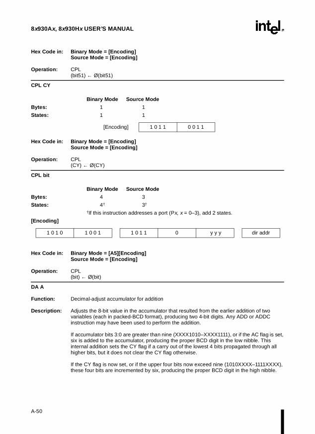
8x930Ax, 8x930Hx USER’S MANUAL
Hex Code in: Binary Mode = [Encoding]Source Mode = [Encoding]
Operation: CPL (bit51) ← Ø(bit51)
CPL CY
Binary Mode Source Mode
Bytes: 1 1
States: 1 1
Hex Code in: Binary Mode = [Encoding]Source Mode = [Encoding]
Operation: CPL (CY) ← Ø(CY)
CPL bit
Binary Mode Source Mode
Bytes: 4 3
States: 4† 3†
†If this instruction addresses a port (Px, x = 0–3), add 2 states.
[Encoding]
Hex Code in: Binary Mode = [A5][Encoding]Source Mode = [Encoding]
Operation: CPL (bit) ← Ø(bit)
DA A
Function: Decimal-adjust accumulator for addition
Description: Adjusts the 8-bit value in the accumulator that resulted from the earlier addition of two variables (each in packed-BCD format), producing two 4-bit digits. Any ADD or ADDC instruction may have been used to perform the addition.
If accumulator bits 3:0 are greater than nine (XXXX1010–XXXX1111), or if the AC flag is set, six is added to the accumulator, producing the proper BCD digit in the low nibble. This internal addition sets the CY flag if a carry out of the lowest 4 bits propagated through all higher bits, but it does not clear the CY flag otherwise.
If the CY flag is now set, or if the upper four bits now exceed nine (1010XXXX–1111XXXX), these four bits are incremented by six, producing the proper BCD digit in the high nibble.
[Encoding] 1 0 1 1 0 0 1 1
1 0 1 0 1 0 0 1 1 0 1 1 0 y y y dir addr
A-50
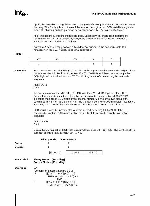
INSTRUCTION SET REFERENCE
Again, this sets the CY flag if there was a carry out of the upper four bits, but does not clear the carry. The CY flag thus indicates if the sum of the original two BCD variables is greater than 100, allowing multiple-precision decimal addition. The OV flag is not affected.
All of this occurs during one instruction cycle. Essentially, this instruction performs the decimal conversion by adding 00H, 06H, 60H, or 66H to the accumulator, depending on initial accumulator and PSW conditions.
Note: DA A cannot simply convert a hexadecimal number in the accumulator to BCD notation, nor does DA A apply to decimal subtraction.
Flags:
Example: The accumulator contains 56H (01010110B), which represents the packed BCD digits of the decimal number 56. Register 3 contains 67H (01100111B), which represents the packed BCD digits of the decimal number 67. The CY flag is set. After executing the instruction sequence
ADDC A,R3 DA A
the accumulator contains 0BEH (10111110) and the CY and AC flags are clear. The Decimal Adjust instruction then alters the accumulator to the value 24H (00100100B), indicating the packed BCD digits of the decimal number 24, the lower two digits of the decimal sum of 56, 67, and the carry-in. The CY flag is set by the Decimal Adjust instruction, indicating that a decimal overflow occurred. The true sum of 56, 67, and 1 is 124.
BCD variables can be incremented or decremented by adding 01H or 99H. If the accumulator contains 30H (representing the digits of 30 decimal), then the instruction sequence,
ADD A,#99H DA A
leaves the CY flag set and 29H in the accumulator, since 30 + 99 = 129. The low byte of the sum can be interpreted to mean 30 – 1 = 29.
Binary Mode Source Mode
Bytes: 1 1
States: 1 1
Hex Code in: Binary Mode = [Encoding]Source Mode = [Encoding]
Operation: DA (Contents of accumulator are BCD) IF [[(A.3:0) > 9] V [(AC) = 1]] THEN (A.3:0) ← (A.3:0) + 6 AND IF [[(A.7:4) > 9] V [(CY) = 1]] THEN (A.7:4) ← (A.7:4) + 6
CY AC OV N Z
3 — — 3 3
[Encoding] 1 1 0 1 0 1 0 0
A-51

8x930Ax, 8x930Hx USER’S MANUAL
DEC byte
Function: Decrement
Description: Decrements the specified byte variable by 1. An original value of 00H underflows to 0FFH. Four operands addressing modes are allowed: accumulator, register, direct, or register-indirect.
Note: When this instruction is used to modify an output port, the value used as the original port data is read from the output data latch, not the input pins.
Flags:
Example: Register 0 contains 7FH (01111111B). On-chip RAM locations 7EH and 7FH contain 00H and 40H, respectively. After executing the instruction sequence
DEC @R0 DEC R0 DEC @R0
register 0 contains 7EH and on-chip RAM locations 7EH and 7FH are set to 0FFH and 3FH, respectively.
Variations
DEC A
Binary Mode Source Mode
Bytes: 1 1
States: 1 1
Hex Code in: Binary Mode = [Encoding]Source Mode = [Encoding]
Operation: DEC (A) ← (A) – 1
DEC dir8
Binary Mode Source Mode
Bytes: 2 2
States: 2† 2†
†If this instruction addresses a port (Px, x = 0–3), add 2 states.
CY AC OV N Z
— — — 3 3
[Encoding] 0 0 0 1 0 1 0 0
[Encoding] 0 0 0 1 0 1 0 1 dir addr
A-52

INSTRUCTION SET REFERENCE
Hex Code in: Binary Mode = [Encoding]Source Mode = [Encoding]
Operation: DEC (dir8) ← (dir8) – 1
DEC @Ri
Binary Mode Source Mode
Bytes: 1 2
States: 3 4
Hex Code in: Binary Mode = [Encoding]Source Mode = [A5][Encoding]
Operation: DEC ((Ri)) ← ((Ri)) – 1
DEC Rn
Binary Mode Source Mode
Bytes: 1 2
States: 1 2
Hex Code in: Binary Mode = [Encoding]Source Mode = [A5][Encoding]
Operation: DEC (Rn) ← (Rn) – 1
DEC <dest>,<src>
Function: Decrement
Description: Decrements the specified variable at the destination operand by 1, 2, or 4. An original value of 00H underflows to 0FFH.
Flags:
Example: Register 0 contains 7FH (01111111B). After executing the instruction sequence
DEC R0,#1
register 0 contains 7EH.
Variations
[Encoding] 0 0 0 1 0 1 1 i
[Encoding] 0 0 0 1 1 r r r
CY AC OV N Z
— — — 3 3
A-53

8x930Ax, 8x930Hx USER’S MANUAL
DEC Rm,#short
Binary Mode Source Mode
Bytes: 3 2
States: 2 1
Hex Code in: Binary Mode = [A5][Encoding]Source Mode = [Encoding]
Operation: DEC (Rm) ← (Rm) – #short
DEC WRj,#short
Binary Mode Source Mode
Bytes: 3 2
States: 2 1
Hex Code in: Binary Mode = [A5][Encoding]Source Mode = [Encoding]
Operation: DEC (WRj) ← (WRj) – #short
DEC DRk,#short
Binary Mode Source Mode
Bytes: 3 2
States: 5 4
Hex Code in: Binary Mode = [A5][Encoding]Source Mode = [Encoding]
Operation: DEC (DRk) ← (DRk) – #short
DIV <dest>,<src>
Function: Divide
Description: Divides the unsigned integer in the register by the unsigned integer operand in register addressing mode and clears the CY and OV flags.
[Encoding] 0 0 0 1 1 0 1 1 s s s s 0 1 v v
[Encoding] 0 0 0 1 1 0 1 1 t t t t 0 1 v v
[Encoding] 0 0 0 1 1 0 1 1 u u u u 1 1 v v
A-54
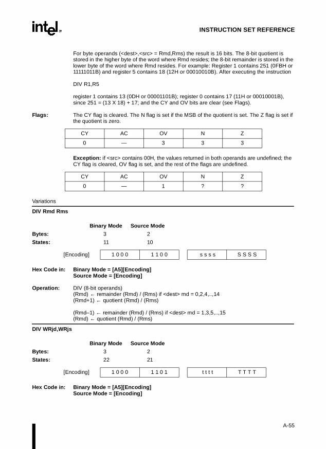
INSTRUCTION SET REFERENCE
For byte operands (<dest>,<src> = Rmd,Rms) the result is 16 bits. The 8-bit quotient is stored in the higher byte of the word where Rmd resides; the 8-bit remainder is stored in the lower byte of the word where Rmd resides. For example: Register 1 contains 251 (0FBH or 11111011B) and register 5 contains 18 (12H or 00010010B). After executing the instruction
DIV R1,R5
register 1 contains 13 (0DH or 00001101B); register 0 contains 17 (11H or 00010001B), since 251 = (13 X 18) + 17; and the CY and OV bits are clear (see Flags).
Flags: The CY flag is cleared. The N flag is set if the MSB of the quotient is set. The Z flag is set if the quotient is zero.
Exception: if <src> contains 00H, the values returned in both operands are undefined; the CY flag is cleared, OV flag is set, and the rest of the flags are undefined.
Variations
DIV Rmd Rms
Binary Mode Source Mode
Bytes: 3 2
States: 11 10
Hex Code in: Binary Mode = [A5][Encoding]Source Mode = [Encoding]
Operation: DIV (8-bit operands) (Rmd) ← remainder (Rmd) / (Rms) if <dest> md = 0,2,4,..,14(Rmd+1) ← quotient (Rmd) / (Rms)
(Rmd–1) ← remainder (Rmd) / (Rms) if <dest> md = 1,3,5,..,15(Rmd) ← quotient (Rmd) / (Rms)
DIV WRjd,WRjs
Binary Mode Source Mode
Bytes: 3 2
States: 22 21
Hex Code in: Binary Mode = [A5][Encoding]Source Mode = [Encoding]
CY AC OV N Z
0 — 3 3 3
CY AC OV N Z
0 — 1 ? ?
[Encoding] 1 0 0 0 1 1 0 0 s s s s S S S S
[Encoding] 1 0 0 0 1 1 0 1 t t t t T T T T
A-55

8x930Ax, 8x930Hx USER’S MANUAL
Operation: DIV (16-bit operands) (WRjd) ← remainder (WRjd) / (WRjs) if <dest> jd = 0, 4, 8,... 28(WRjd+2) ← quotient (WRjd) / (WRjs)
(WRjd–2) ← remainder (WRjd) / (WRjs) if <dest> jd = 2, 6, 10,... 30(WRjd) ← quotient (WRjd) / (WRjs)
For word operands (<dest>,<src> = WRjd,WRjs) the 16-bit quotient is in WR(jd+2), and the 16-bit remainder is in WRjd. For example, for a destination register WR4, assume the quotient is 1122H and the remainder is 3344H. Then, the results are stored in these register file locations:
DIV AB
Function: Divide
Description: Divides the unsigned 8-bit integer in the accumulator by the unsigned 8-bit integer in register B. The accumulator receives the integer part of the quotient; register B receives the integer remainder. The CY and OV flags are cleared.
Exception: if register B contains 00H, the values returned in the accumulator and register B are undefined; the CY flag is cleared and the OV flag is set.
Flags:
For division by zero:
Hex Code in: Binary Mode = [Encoding]Source Mode = [Encoding]
Example: The accumulator contains 251 (0FBH or 11111011B) and register B contains 18 (12H or 00010010B). After executing the instruction
DIV AB
the accumulator contains 13 (0DH or 00001101B); register B contains 17 (11H or 00010001B), since 251 = (13 X 18) + 17; and the CY and OV flags are clear.
Binary Mode Source Mode
Bytes: 1 1
States: 10 10
Location 4 5 6 7
Contents 33H 44H 11H 22H
CY AC OV N Z
0 — 3 3 3
CY AC OV N Z
0 — 1 ? ?
[Encoding] 1 0 0 0 0 1 0 0
A-56

INSTRUCTION SET REFERENCE
Hex Code in: Binary Mode = [Encoding]Source Mode = [Encoding]
Operation: DIV (A) ← quotient (A)/(B) (B) ← remainder (A)/(B)
DJNZ <byte>,<rel–addr>
Function: Decrement and jump if not zero
Description: Decrements the specified location by 1 and branches to the address specified by the second operand if the resulting value is not zero. An original value of 00H underflows to 0FFH. The branch destination is computed by adding the signed relative-displacement value in the last instruction byte to the PC, after incrementing the PC to the first byte of the following instruction.
The location decremented may be a register or directly addressed byte.
Note: When this instruction is used to modify an output port, the value used as the original port data is read from the output data latch, not the input pins.
Flags:
Example: The on-chip RAM locations 40H, 50H, and 60H contain 01H, 70H, and 15H, respectively. After executing the following instruction sequence
DJNZ 40H,LABEL1 DJNZ 50H,LABEL2 DJNZ 60H,LABEL
on-chip RAM locations 40H, 50H, and 60H contain 00H, 6FH, and 14H, respectively, and program execution continues at label LABEL2. (The first jump was not taken because the result was zero.)
This instruction provides a simple way of executing a program loop a given number of times, or for adding a moderate time delay (from 2 to 512 machine cycles) with a single instruction.
The instruction sequence,
toggles P1.7 eight times, causing four output pulses to appear at bit 7 of output Port 1. Each pulse lasts three states: two for DJNZ and one to alter the pin.
Variations
CY AC OV N Z
— — — 3 3
TOGGLE:MOV R2,#8CPL P1.7 DJNZ R2,TOGGLE
A-57

8x930Ax, 8x930Hx USER’S MANUAL
DJNZ dir8,rel
Binary Mode Source Mode
Not Taken Taken Not Taken Taken
Bytes: 3 3 3 3
States: 3 6 3 6
Hex Code in: Binary Mode = [Encoding]Source Mode = [Encoding]
Operation: DJNZ (PC) ← (PC) + 2 (dir8) ← (dir8) – 1 IF (dir8) > 0 or (dir8) < 0 THEN (PC) ← (PC) + rel
DJNZ Rn,rel
Binary Mode Source Mode
Not Taken Taken Not Taken Taken
Bytes: 2 2 3 3
States: 2 5 3 6
Hex Code in: Binary Mode = [Encoding]Source Mode = [A5][Encoding]
Operation: DJNZ (PC) ← (PC) + 2 (Rn) ← (Rn) – 1 IF (Rn) > 0 or (Rn) < 0 THEN (PC) ← (PC) + rel
ECALL <dest>
Function: Extended call
Description: Calls a subroutine located at the specified address. The instruction adds four to the program counter to generate the address of the next instruction and then pushes the 24-bit result onto the stack (high byte first), incrementing the stack pointer by three. The 8 bits of the high word and the 16 bits of the low word of the PC are then loaded, respectively, with the second, third and fourth bytes of the ECALL instruction. Program execution continues with the instruction at this address. The subroutine may therefore begin anywhere in the full 16-Mbyte memory space.
Flags:
[Encoding] 1 1 0 1 0 1 0 1 direct addr rel. addr
[Encoding] 1 1 0 1 1 r r r rel. addr
CY AC OV N Z
— — — — —
A-58

INSTRUCTION SET REFERENCE
Example: The stack pointer contains 07H and the label “SUBRTN” is assigned to program memory location 123456H. After executing the instruction
ECALL SUBRTN
at location 012345H, SP contains 0AH; on-chip RAM locations 08H, 09H and 0AH contain 01H, 23H and 45H, respectively; and the PC contains 123456H.
Variations
ECALL addr24
Binary Mode Source Mode
Bytes: 5 4
States: 14 13
Hex Code in: Binary Mode = [A5][Encoding]Source Mode = [Encoding]
Operation: ECALL(PC) ← (PC) + 4(SP) ← (SP) + 1((SP)) ← (PC.23:16) (SP) ← (SP) + 1((SP)) ← (PC.15:8) (SP) ← (SP) + 1((SP)) ← (PC.7:0) (PC) ← (addr.23:0)
ECALL @DRk
Binary Mode Source Mode
Bytes: 3 2
States: 12 11
Hex Code in: Binary Mode = [A5][Encoding]Source Mode = [Encoding]
Operation: ECALL(PC) ← (PC) + 4(SP) ← (SP) + 1((SP)) ← (PC.23:16)(SP) ← (SP) + 1((SP)) ← (PC.15:8)(SP) ← (SP) + 1((SP)) ← (PC.7:0) (PC) ← ((DRk))
EJMP <dest>
Function: Extended jump
[Encoding] 1 0 0 1 1 0 1 0 addr23–addr16
addr15–addr8
addr7–addr0
[Encoding] 1 0 0 1 1 0 0 1 u u u u
A-59

8x930Ax, 8x930Hx USER’S MANUAL
Description: Causes an unconditional branch to the specified address by loading the 8 bits of the high order and 16 bits of the low order words of the PC with the second, third, and fourth instruction bytes. The destination may be therefore be anywhere in the full 16-Mbyte memory space.
Flags:
Example: The label "JMPADR" is assigned to the instruction at program memory location 123456H. The instruction is
EJMP JMPADR Variations
EJMP addr24
Binary Mode Source Mode
Bytes: 5 4
States: 6 5
Hex Code in: Binary Mode = [A5][Encoding]Source Mode = [Encoding]
Operation: EJMP(PC) ← (addr.23:0)
EJMP @DRk
Binary Mode Source Mode
Bytes: 3 2
States: 7 6
Hex Code in: Binary Mode =[A5][Encoding]Source Mode = [Encoding]
Operation: EJMP(PC) ← ((DRk))
ERET
Function: Extended return
Description: Pops byte 2, byte 1, and byte 0 of the 3-byte PC successively from the stack and decrements the stack pointer by 3. Program execution continues at the resulting address, which normally is the instruction immediately following ECALL.
Flags: No flags are affected.
CY AC OV N Z
— — — — —
[Encoding] 1 0 0 0 1 0 1 0 addr23–addr16
addr15–addr8
addr7–addr0
[Encoding] 1 0 0 0 1 0 0 1 u u u u
A-60

INSTRUCTION SET REFERENCE
Example: The stack pointer contains 0BH. On-chip RAM locations 08H, 09H and 0AH contain 01H, 23H and 49H, respectively. After executing the instruction
ERET
the stack pointer contains 08H and program execution continues at location 012349H.
Binary Mode Source Mode
Bytes: 3 2
States: 10 9
Hex Code in: Binary Mode = [A5][Encoding]Source Mode = [Encoding]
Operation: ERET
(PC.23:16) ← ((SP)) (SP) ← (SP) – 1(PC.15:8) ← ((SP)) (SP) ← (SP) – 1(PC.7:0) ← ((SP)) (SP) ← (SP) – 1
INC <Byte>
Function: Increment
Description: Increments the specified byte variable by 1. An original value of FFH overflows to 00H. Three addressing modes are allowed for 8-bit operands: register, direct, or register-indirect.
Note: When this instruction is used to modify an output port, the value used as the original port data is read from the output data latch, not the input pins.
Flags:
Example: Register 0 contains 7EH (011111110B) and on-chip RAM locations 7EH and 7FH contain 0FFH and 40H, respectively. After executing the instruction sequence
INC @R0 INC R0 INC @R0
register 0 contains 7FH and on-chip RAM locations 7EH and 7FH contain 00H and 41H, respectively.
Variations
INC A
Binary Mode Source Mode
Bytes: 1 1
States: 1 1
[Encoding] 1 0 1 0 1 0 1 0
CY AC OV N Z
— — — 3 3
[Encoding] 0 0 0 0 0 1 0 0
A-61

8x930Ax, 8x930Hx USER’S MANUAL
Hex Code in: Binary Mode = [Encoding]Source Mode = [Encoding]
Operation: INC (A) ← (A) + 1
INC dir8
Binary Mode Source Mode
Bytes: 2 2
States: 2† 2†
†If this instruction addresses a port (Px, x = 0–3), add 2 states.
Hex Code in: Binary Mode = [Encoding]Source Mode = [Encoding]
Operation: INC (dir8) ← (dir8) + 1
INC @Ri
Binary Mode Source Mode
Bytes: 1 2
States: 3 4
Hex Code in: Binary Mode = [Encoding]Source Mode = [A5][Encoding]
Operation: INC ((Ri) ← ((Ri)) + 1
INC Rn
Binary Mode Source Mode
Bytes: 1 2
States: 1 2
Hex Code in: Binary Mode = [Encoding]Source Mode = [A5][Encoding]
Operation: INC (Rn) ← (Rn) + 1
INC <dest>,<src>
Function: Increment
Description : Increments the specified variable by 1, 2, or 4. An original value of 0FFH overflows to 00H.
[Encoding] 0 0 0 0 0 1 0 1 direct addr
[Encoding] 0 0 0 0 0 1 1 i
[Encoding] 0 0 0 0 1 r r r
A-62

INSTRUCTION SET REFERENCE
Flags:
Example: Register 0 contains 7EH (011111110B). After executing the instruction
INC R0,#1
register 0 contains 7FH.Variations
INC Rm,#short
Binary Mode Source Mode
Bytes: 3 2
States: 2 1
Hex Code in: Binary Mode = [A5][Encoding]Source Mode = [Encoding]
Operation: INC (Rm) ← (Rm) + #short
INC WRj,#short
Binary Mode Source Mode
Bytes: 3 2
States: 2 1
Hex Code in: Binary Mode = [A5][Encoding]Source Mode = [Encoding]
Operation: INC (WRj) ← (WRj) + #short
INC DRk,#short
Binary Mode Source Mode
Bytes: 3 2
States: 4 3
Hex Code in: Binary Mode = [A5][Encoding]Source Mode = [Encoding]
Operation: INC (DRk) ← (DRk) + #shortdata pointer
CY AC OV N Z
— — — 3 3
[Encoding] 0 0 0 0 1 0 1 1 s s s s 00 v v
[Encoding] 0 0 0 0 1 0 1 1 t t t t 01 v v
[Encoding] 0 0 0 0 1 0 1 1 u u u u 11 v v
A-63

8x930Ax, 8x930Hx USER’S MANUAL
INC DPTR
Function: Increment data pointer
Description: Increments the 16-bit data pointer by one. A 16-bit increment (modulo 216) is performed; an overflow of the low byte of the data pointer (DPL) from 0FFH to 00H increments the high byte of the data pointer (DPH) by one. An overflow of the high byte (DPH) does not increment the high word of the extended data pointer (DPX = DR56).
Flags:
Example: Registers DPH and DPL contain 12H and 0FEH, respectively. After the instruction sequence
INC DPTR INC DPTR INC DPTR
DPH and DPL contain 13H and 01H, respectively.
Binary Mode Source Mode
Bytes: 1 1
States: 1 1
Hex Code in: Binary Mode = [Encoding]Source Mode = [Encoding]
Operation: INC (DPTR) ← (DPTR) + 1
JB bit51,rel JB bit,rel
Function: Jump if bit set
Description: If the specified bit is a one, jump to the address specified; otherwise proceed with the next instruction. The branch destination is computed by adding the signed relative displacement in the third instruction byte to the PC, after incrementing the PC to the first byte of the next instruction. The bit tested is not modified.
Flags:
CY AC OV N Z
— — — 3 3
[Encoding] 1 0 1 0 0 0 1 1
CY AC OV N Z
— — — — —
A-64

INSTRUCTION SET REFERENCE
Example: Input port 1 contains 11001010B and the accumulator contains 56 (01010110B). After the instruction sequence
JB P1.2,LABEL1 JB ACC.2,LABEL2
program execution continues at label LABEL2.Variations
JB bit51,rel
Binary Mode Source Mode
Not Taken Taken Not Taken Taken
Bytes: 3 3 3 3
States: 2 5 2 5
Hex Code in: Binary Mode = [Encoding]Source Mode = [Encoding]
Operation: JB (PC) ← (PC) + 3 IF (bit51) = 1 THEN (PC) ← (PC) + rel
JB bit,rel
Binary Mode Source Mode
Not Taken Taken Not Taken Taken
Bytes: 5 5 4 4
States: 4 7 3 6
[Encoding]
Hex Code in: Binary Mode = [A5][Encoding]Source Mode = [Encoding]
Operation: JB (PC) ← (PC) + 3 IF (bit) = 1 THEN (PC) ← (PC) + rel
[Encoding] 0 0 1 0 0 0 0 0 bit addr rel. addr
1 0 1 0 1 0 0 1 0 0 1 0 0 y y direct addr rel. addr
A-65

8x930Ax, 8x930Hx USER’S MANUAL
JBC bit51,rel JBC bit,rel
Function: Jump if bit is set and clear bit Description: If the specified bit is one, branch to the specified address; otherwise proceed with the next
instruction. The bit is not cleared if it is already a zero. The branch destination is computed by adding the signed relative displacement in the third instruction byte to the PC, after incre-menting the PC to the first byte of the next instruction.
Note: When this instruction is used to test an output pin, the value used as the original data is read from the output data latch, not the input pin.
Flags:
Example: The accumulator contains 56H (01010110B). After the instruction sequence
JBC ACC.3,LABEL1 JBC ACC.2,LABEL2
the accumulator contains 52H (01010010B) and program execution continues at label LABEL2.
Variations
JBC bit51,rel
Binary Mode Source Mode
Not Taken Taken Not Taken Taken
Bytes: 3 3 3 3
States: 4 7 4 7
Hex Code in: Binary Mode = [Encoding]Source Mode = [Encoding]
Operation: JBC (PC) ← (PC) + 3 IF (bit51) = 1 THEN (bit51) ← 0 (PC) ← (PC) + rel
JBC bit,rel
Binary Mode Source Mode
Not Taken Taken Not Taken Taken
Bytes: 5 5 4 4
States: 4 7 3 6
CY AC OV N Z
— — — — —
[Encoding] 0 0 0 1 0 0 0 0 bit addr rel. addr
A-66

INSTRUCTION SET REFERENCE
[Encoding]
Hex Code in: Binary Mode = [A5][Encoding]Source Mode = [Encoding]
Operation: JBC (PC) ← (PC) + 3 IF (bit51) = 1 THEN (bit51) ← 0 (PC) ← (PC) + rel
JC rel
Function: Jump if carry is set
Description: If the CY flag is set, branch to the address specified; otherwise proceed with the next instruction. The branch destination is computed by adding the signed relative displacement in the second instruction byte to the PC, after incrementing the PC twice.
Flags:
Example: The CY flag is clear. After the instruction sequence
JC LABEL1 CPL CY JC LABEL 2
the CY flag is set and program execution continues at label LABEL2.
Binary Mode Source Mode
Not Taken Taken Not Taken Taken
Bytes: 2 2 2 2
States: 1 4 1 4
Hex Code in: Binary Mode = [Encoding]Source Mode = [Encoding]
Operation: JC (PC) ← (PC) + 2 IF (CY) = 1 THEN (PC) ← (PC) + rel
1 0 1 0 1 0 0 1 0 0 0 1 0 y y y direct addr rel. addr
CY AC OV N Z
! — — — —
[Encoding] 0 1 0 0 0 0 0 0 rel. addr
A-67

8x930Ax, 8x930Hx USER’S MANUAL
JE rel
Function: Jump if equal
Description: If the Z flag is set, branch to the address specified; otherwise proceed with the next instruction. The branch destination is computed by adding the signed relative displacement in the second instruction byte to the PC, after incrementing the PC twice.
Flags:
Example: The Z flag is set. After executing the instruction
JE LABEL1
program execution continues at label LABEL1.
Binary Mode Source Mode
Not Taken Taken Not Taken Taken
Bytes: 3 3 2 2
States: 2 5 1 4
Hex Code in: Binary Mode = [A5][Encoding]Source Mode = [Encoding]
Operation: JE(PC) ← (PC) + 2 IF (Z) = 1 THEN (PC) ← (PC) + rel
JG rel
Function: Jump if greater than
Description: If the Z flag and the CY flag are both clear, branch to the address specified; otherwise proceed with the next instruction. The branch destination is computed by adding the signed relative displacement in the second instruction byte to the PC, after incrementing the PC twice.
Flags:
Example: The instruction
JG LABEL1
causes program execution to continue at label LABEL1 if the Z flag and the CY flag are both clear.
CY AC OV N Z
— — — — !
[Encoding] 0 1 1 0 1 0 0 0 rel. addr
CY AC OV N Z
— — — ! —
A-68

INSTRUCTION SET REFERENCE
Binary Mode Source Mode
Not Taken Taken Not Taken Taken
Bytes: 3 3 2 2
States: 2 5 1 4
Hex Code in: Binary Mode = [A5][Encoding]Source Mode = [Encoding]
Operation: JG(PC) ← (PC) + 2 IF (Z) = 0 AND (CY) = 0 THEN (PC) ← (PC) + rel
JLE rel
Function: Jump if less than or equal
Description: If the Z flag or the CY flag is set, branch to the address specified; otherwise proceed with the next instruction. The branch destination is computed by adding the signed relative displacement in the second instruction byte to the PC, after incrementing the PC twice.
Flags:
Example: The instruction
JLE LABEL1
causes program execution to continue at LABEL1 if the Z flag or the CY flag is set.
Binary Mode Source Mode
Not Taken Taken Not Taken Taken
Bytes: 3 3 2 2
States: 2 5 1 4
Hex Code in: Binary Mode = [A5][Encoding]Source Mode = [Encoding]
Operation: JLE(PC) ← (PC) + 2 IF (Z) = 1 OR (CY) = 1 THEN (PC) ← (PC) + rel
[Encoding] 0 0 1 1 1 0 0 0 rel. addr
CY AC OV N Z
— — — ! !
[Encoding] 0 0 1 0 1 0 0 0 rel. addr
A-69

8x930Ax, 8x930Hx USER’S MANUAL
JMP @A+DPTR
Function: Jump indirect
Description: Add the 8-bit unsigned contents of the accumulator with the 16-bit data pointer and load the resulting sum into the lower 16 bits of the program counter. This is the address for subsequent instruction fetches. The contents of the accumulator and the data pointer are not affected.
Flags:
Example: The accumulator contains an even number from 0 to 6. The following sequence of instruc-tions branch to one of four AJMP instructions in a jump table starting at JMP_TBL:
If the accumulator contains 04H at the start this sequence, execution jumps to LABEL2. Remember that AJMP is a two-byte instruction, so the jump instructions start at every other address.
Binary Mode Source Mode
Bytes: 1 1
States: 5 5
Hex Code in: Binary Mode = [Encoding]Source Mode = [Encoding]
Operation: JMP (PC.15:0) ← (A) + (DPTR)
JNB bit51,relJNB bit,rel
Function: Jump if bit not set
Description: If the specified bit is clear, branch to the specified address; otherwise proceed with the next instruction. The branch destination is computed by adding the signed relative displacement in the third instruction byte to the PC, after incrementing the PC to the first byte of the next instruction. The bit tested is not modified.
CY AC OV N Z
— — — — —
JMP_TBL:
MOVJMPAJMPAJMPAJMPAJMP
DPTR,#JMP_TBL@A+DPTRLABEL0LABEL1LABEL2LABEL3
[Encoding] 0 1 1 1 0 0 1 1
A-70

INSTRUCTION SET REFERENCE
Flags:
Example: Input port 1 contains 11001010B and the accumulator contains 56H (01010110B). After executing the instruction sequence
JNB P1.3,LABEL1 JNB ACC.3,LABEL2
program execution continues at label LABEL2.
Variations
JNB bit51,rel
Binary Mode Source Mode
Not Taken Taken Not Taken Taken
Bytes: 3 3 3 3
States: 2 5 2 5
Hex Code in: Binary Mode = [Encoding]Source Mode = [Encoding]
Operation: JNB (PC) ← (PC) + 3 IF (bit51) = 0 THEN (PC) ← (PC) + rel
JNB bit,rel
Binary Mode Source Mode
Not Taken Taken Not Taken Taken
Bytes: 5 5 4 4
States: 4 7 3 6
[Encoding]
Hex Code in: Binary Mode = [A5][Encoding]Source Mode = [Encoding]
Operation: JNB (PC) ← (PC) + 3 IF (bit) = 0 THEN (PC) ← (PC) + rel
CY AC OV N Z
— — — — —
[Encoding] 0 0 1 1 0 0 0 0 bit addr rel. addr
1 0 1 0 1 0 0 1 0 0 1 1 0 y y direct addr rel. addr
A-71

8x930Ax, 8x930Hx USER’S MANUAL
JNC rel
Function: Jump if carry not set
Description: If the CY flag is clear, branch to the address specified; otherwise proceed with the next instruction. The branch destination is computed by adding the signed relative displacement in the second instruction byte to the PC, after incrementing the PC twice to point to the next instruction. The CY flag is not modified.
Flags:
Example: The CY flag is set. The instruction sequence
JNC LABEL1 CPL CY JNC LABEL2
clears the CY flag and causes program execution to continue at label LABEL2.
Binary Mode Source Mode
Not Taken Taken Not Taken Taken
Bytes: 2 2 2 2
States: 1 4 1 4
Hex Code in: Binary Mode = [Encoding]Source Mode = [Encoding]
Operation: JNC (PC) ← (PC) + 2 IF (CY) = 0 THEN (PC) ← (PC) + rel
JNE rel
Function: Jump if not equal
Description: If the Z flag is clear, branch to the address specified; otherwise proceed with the next instruction. The branch destination is computed by adding the signed relative displacement in the second instruction byte to the PC, after incrementing the PC twice.
Flags:
Example: The instruction
JNE LABEL1
causes program execution to continue at LABEL1 if the Z flag is clear.
CY AC OV N Z
! — — — —
[Encoding] 0 1 0 1 0 0 0 0 rel. addr
CY AC OV N Z
— — — — !
A-72

INSTRUCTION SET REFERENCE
Binary Mode Source Mode
Not Taken Taken Not Taken Taken
Bytes: 3 3 2 2
States: 2 5 1 4
Hex Code in: Binary Mode = [A5][Encoding]Source Mode = [Encoding]
Operation: JNE(PC) ← (PC) + 2 IF (Z) = 0 THEN (PC) ← (PC) + rel
JNZ rel
Function: Jump if accumulator not zero
Description: If any bit of the accumulator is set, branch to the specified address; otherwise proceed with the next instruction. The branch destination is computed by adding the signed relative displacement in the second instruction byte to the PC, after incrementing the PC twice. The accumulator is not modified.
Flags:
Example: The accumulator contains 00H. After executing the instruction sequence
JNZ LABEL1 INC A JNZ LABEL2
the accumulator contains 01H and program execution continues at label LABEL2.
Binary Mode Source Mode
Not Taken Taken Not Taken Taken
Bytes: 2 2 2 2
States: 2 5 2 5
Hex Code in: Binary Mode = [Encoding]Source Mode = [Encoding]
Operation: JNZ (PC) ← (PC) + 2 IF (A) ≠ 0 THEN (PC) ← (PC) + rel
[Encoding] 0 1 1 1 1 0 0 0 rel. addr
CY AC OV N Z
— — — — !
[Encoding] 0 1 1 1 0 0 0 0 rel. addr
A-73

8x930Ax, 8x930Hx USER’S MANUAL
JSG rel
Function: Jump if greater than (signed)
Description: If the Z flag is clear AND the N flag and the OV flag have the same value, branch to the address specified; otherwise proceed with the next instruction. The branch destination is computed by adding the signed relative displacement in the second instruction byte to the PC, after incrementing the PC twice.
Flags:
Example: The instruction
JSG LABEL1
causes program execution to continue at LABEL1 if the Z flag is clear AND the N flag and the OV flag have the same value.
Binary Mode Source Mode
Not Taken Taken Not Taken Taken
Bytes: 3 3 2 2
States: 2 5 1 4
Hex Code in: Binary Mode = [A5][Encoding]Source Mode = [Encoding]
Operation: JSG(PC) ← (PC) + 2 IF [(N) = 0 AND (N) = (OV)] THEN (PC) ← (PC) + rel
JSGE rel
Function: Jump if greater than or equal (signed)
Description: If the N flag and the OV flag have the same value, branch to the address specified; otherwise proceed with the next instruction. The branch destination is computed by adding the signed relative displacement in the second instruction byte to the PC, after incrementing the PC twice.
Flags:
CY AC OV N Z
— — ! ! !
[Encoding] 0 0 0 1 1 0 0 0 rel. addr
CY AC OV N Z
— — ! ! !
A-74
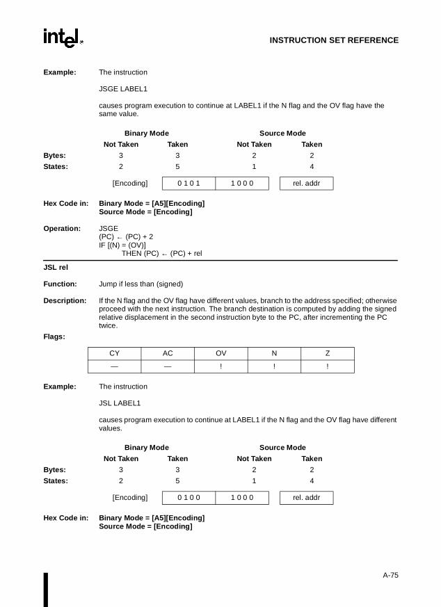
INSTRUCTION SET REFERENCE
Example: The instruction
JSGE LABEL1
causes program execution to continue at LABEL1 if the N flag and the OV flag have the same value.
Binary Mode Source Mode
Not Taken Taken Not Taken Taken
Bytes: 3 3 2 2
States: 2 5 1 4
Hex Code in: Binary Mode = [A5][Encoding]Source Mode = [Encoding]
Operation: JSGE(PC) ← (PC) + 2 IF [(N) = (OV)] THEN (PC) ← (PC) + rel
JSL rel
Function: Jump if less than (signed)
Description: If the N flag and the OV flag have different values, branch to the address specified; otherwise proceed with the next instruction. The branch destination is computed by adding the signed relative displacement in the second instruction byte to the PC, after incrementing the PC twice.
Flags:
Example: The instruction
JSL LABEL1
causes program execution to continue at LABEL1 if the N flag and the OV flag have different values.
Binary Mode Source Mode
Not Taken Taken Not Taken Taken
Bytes: 3 3 2 2
States: 2 5 1 4
Hex Code in: Binary Mode = [A5][Encoding]Source Mode = [Encoding]
[Encoding] 0 1 0 1 1 0 0 0 rel. addr
CY AC OV N Z
— — ! ! !
[Encoding] 0 1 0 0 1 0 0 0 rel. addr
A-75

8x930Ax, 8x930Hx USER’S MANUAL
Operation: JSL(PC) ← (PC) + 2 IF (N) ≠ (OV) THEN (PC) ← (PC) + rel
JSLE rel
Function: Jump if less than or equal (signed)
Description: If the Z flag is set OR if the the N flag and the OV flag have different values, branch to the address specified; otherwise proceed with the next instruction. The branch destination is computed by adding the signed relative displacement in the second instruction byte to the PC, after incrementing the PC twice.
Flags:
Example: The instruction
JSLE LABEL1
causes program execution to continue at LABEL1 if the Z flag is set OR if the the N flag and the OV flag have different values.
Binary Mode Source Mode
Not Taken Taken Not Taken Taken
Bytes: 3 3 2 2
States: 2 5 1 4
Hex Code in: Binary Mode = [A5][Encoding]Source Mode = [Encoding]
Operation: JSLE(PC) ← (PC) + 2 IF (Z) = 1 OR [(N) ≠ (OV)] THEN (PC) ← (PC) + rel
JZ rel
Function: Jump if accumulator zero
Description: If all bits of the accumulator are clear (zero), branch to the address specified; otherwise proceed with the next instruction. The branch destination is computed by adding the signed relative displacement in the second instruction byte to the PC, after incrementing the PC twice. The accumulator is not modified.
Flags:
CY AC OV N Z
— — ! ! !
[Encoding] 0 0 0 0 1 0 0 0 rel. addr
CY AC OV N Z
— — — — !
A-76

INSTRUCTION SET REFERENCE
Example: The accumulator contains 01H. After executing the instruction sequence
JZ LABEL1DEC A JZ LABEL2
the accumulator contains 00H and program execution continues at label LABEL2.
Binary Mode Source Mode
Not Taken Taken Not Taken Taken
Bytes: 2 2 2 2
States: 2 5 2 5
Hex Code in: Binary Mode = [Encoding]Source Mode = [Encoding]
Operation: JZ (PC) ← (PC) + 2 IF (A) = 0 THEN (PC) ← (PC) + rel
LCALL <dest>
Function: Long call
Description: Calls a subroutine located at the specified address. The instruction adds three to the program counter to generate the address of the next instruction and then pushes the 16-bit result onto the stack (low byte first). The stack pointer is incremented by two. The high and low bytes of the PC are then loaded, respectively, with the second and third bytes of the LCALL instruction. Program execution continues with the instruction at this address. The subroutine may therefore begin anywhere in the 64-Kbyte region of memory where the next instruction is located.
Flags:
Example: The stack pointer contains 07H and the label "SUBRTN" is assigned to program memory location 1234H. After executing the instruction
LCALL SUBRTN
at location 0123H, the stack pointer contains 09H, on-chip RAM locations 08H and 09H contain 01H and 26H, and the PC contains 1234H.
LCALL addr16
Binary Mode Source Mode
Bytes: 3 3
States: 9 9
[Encoding] 0 1 1 0 0 0 0 0 rel. addr
CY AC OV N Z
— — — — —
[Encoding] 0 0 0 1 0 0 1 0 addr15–addr8
addr7–addr0
A-77

8x930Ax, 8x930Hx USER’S MANUAL
Hex Code in: Binary Mode = [Encoding] Source Mode = [Encoding]
Operation: LCALL (PC) ← (PC) + 3 (SP) ← (SP) + 1 ((SP)) ← (PC.7:0) (SP) ← (SP) + 1 ((SP)) ← (PC.15:8) (PC) ← (addr.15:0)
LCALL @WRj
Binary Mode Source Mode
Bytes: 3 2
States: 9 8
Hex Code in: Binary Mode = [A5][Encoding] Source Mode = [Encoding]
Operation: LCALL (PC) ← (PC) + 3 (SP) ← (SP) + 1 ((SP)) ← (PC.7:0) (SP) ← (SP) + 1 ((SP)) ← (PC.15:8) (PC) ← ((WRj))
LJMP <dest>
Function: Long Jump
Description: Causes an unconditional branch to the specified address, by loading the high and low bytes of the PC (respectively) with the second and third instruction bytes. The destination may therefore be anywhere in the 64-Kbyte memory region where the next instruction is located.
Flags:
Example: The label "JMPADR" is assigned to the instruction at program memory location 1234H. After executing the instruction
LJMP JMPADR
at location 0123H, the program counter contains 1234H.
[Encoding] 1 0 0 1 1 0 0 1 t t t t 0 1 0 0
CY AC OV N Z
— — — — —
A-78

INSTRUCTION SET REFERENCE
LJMP addr16
Binary Mode Source Mode
Bytes: 3 3
States: 5 5
Hex Code in: Binary Mode = [Encoding] Source Mode = [Encoding]
Operation: LJMP (PC) ← (addr.15:0)
LJMP @WRj
Binary Mode Source Mode
Bytes: 3 2
States: 6 5
Hex Code in: Binary Mode = [A5][Encoding] Source Mode = [Encoding]
Operation: LJMP (PC) ← ((WRj))
MOV <dest>,<src>
Function: Move byte variable
Description: Copies the byte variable specified by the second operand into the location specified by the first operand. The source byte is not affected.
This is by far the most flexible operation. Twenty-four combinations of source and destination addressing modes are allowed.
Flags:
[Encoding] 0 0 0 0 0 0 1 0 addr15–addr8
addr7–addr0
[Encoding] 1 0 0 0 1 0 0 1 t t t t 0 1 0 0
CY AC OV N Z
— — — — —
A-79

8x930Ax, 8x930Hx USER’S MANUAL
Example: On-chip RAM location 30H contains 40H, on-chip RAM location 40H contains 10H, and input port 1 contains 11001010B (0CAH). After executing the instruction sequence
register 0 contains 30H, the accumulator and register 1 contain 40H, register B contains 10H, and on-chip RAM location 40H and output port 2 contain 0CAH (11001010B).
Variations
MOV A,#data
Binary Mode Source Mode
Bytes: 2 2
States: 1 1
Hex Code in: Binary Mode = [Encoding] Source Mode = [Encoding]
Operation: MOV (A) ← #data
MOV dir8,#data
Binary Mode Source Mode
Bytes: 3 3
States: 3† 3†
†If this instruction addresses a port (Px, x = 0–3), add 1 state.
Hex Code in: Binary Mode = [Encoding] Source Mode = [Encoding]
Operation: MOV (dir8) ← #data
MOV @Ri,#data
Binary Mode Source Mode
Bytes: 2 3
States: 3 4
Hex Code in: Binary Mode = [Encoding] Source Mode = [A5][Encoding]
MOVMOVMOVMOVMOVMOV
R0,#30HA,@R0R1,AB,@R1@R1,P1P2,P1
;R0 < = 30H;A < = 40H;R1 < = 40H;B < = 10H;RAM (40H) < = 0CAH;P2 #0CAH
[Encoding] 0 1 1 1 0 1 0 0 immed. data
[Encoding] 0 1 1 1 0 1 0 1 direct addr immed. data
[Encoding] 0 1 1 1 0 1 1 i immed. data
A-80

INSTRUCTION SET REFERENCE
Operation: MOV ((Ri)) ← #data
MOV Rn,#data
Binary Mode Source Mode
Bytes: 2 3
States: 1 2
Hex Code in: Binary Mode = [Encoding] Source Mode = [A5][Encoding]
Operation: MOV (Rn) ← #data
MOV dir8,dir8
Binary Mode Source Mode
Bytes: 3 3
States: 3 3
Hex Code in: Binary Mode = [Encoding] Source Mode = [Encoding]
Operation: MOV (dir8) ← (dir8)
MOV dir8,@Ri
Binary Mode Source Mode
Bytes: 2 3
States: 3 4
Hex Code in: Binary Mode = [Encoding] Source Mode = [A5][Encoding]
Operation: MOV (dir8) ← ((Ri))
MOV dir8,Rn
Binary Mode Source Mode
Bytes: 2 3
States: 2† 3†
†If this instruction addresses a port (Px, x = 0–3), add 1 state.
[Encoding] 0 1 1 1 1 r r r r immed. data
[Encoding] 1 0 0 0 0 1 0 1 direct addr direct addr
[Encoding] 1 0 0 0 0 1 1 i direct addr
[Encoding] 1 0 0 0 1 r r r direct addr
A-81

8x930Ax, 8x930Hx USER’S MANUAL
Hex Code in: Binary Mode = [Encoding] Source Mode = [A5][Encoding]
Operation: MOV (dir8) ← (Rn)
MOV @Ri,dir8
Binary Mode Source Mode
Bytes: 2 3
States: 3 4
Hex Code in: Binary Mode = [Encoding] Source Mode = [A5][Encoding]
Operation: MOV ((Ri)) ← (dir8)
MOV Rn,dir8
Binary Mode Source Mode
Bytes: 2 3
States: 1† 2†
†If this instruction addresses a port (Px, x = 0–3), add 1 state.
Hex Code in: Binary Mode = [Encoding] Source Mode = [A5][Encoding]
Operation: MOV (Rn) ← (dir8)
MOV A,dir8
Binary Mode Source Mode
Bytes: 2 2
States: 1† 1†
†If this instruction addresses a port (Px, x = 0–3), add 1 state.
Hex Code in: Binary Mode = [Encoding] Source Mode = [Encoding]
Operation: MOV (A) ← (dir8)
[Encoding] 1 0 1 0 0 1 1 i direct addr
[Encoding] 1 0 1 0 1 r r r direct addr
[Encoding] 1 1 1 0 0 1 0 1 direct addr
A-82

INSTRUCTION SET REFERENCE
MOV A,@Ri
Binary Mode Source Mode
Bytes: 1 2
States: 2 3
Hex Code in: Binary Mode = [Encoding] Source Mode = [A5][Encoding]
Operation: MOV (A) ← ((Ri))
MOV A,Rn
Binary Mode Source Mode
Bytes: 1 2
States: 1 2
Hex Code in: Binary Mode = [Encoding] Source Mode = [A5][Encoding]
Operation: MOV (A) ← (Rn)
MOV dir8,A
Binary Mode Source Mode
Bytes: 2 2
States: 2† 2†
†If this instruction addresses a port (Px, x = 0–3), add 1 state.
Hex Code in: Binary Mode = [Encoding] Source Mode = [Encoding]
Operation: MOV (dir8) ← (A)
MOV @Ri,A
Binary Mode Source Mode
Bytes: 1 2
States: 3 4
[Encoding] 1 1 1 0 0 1 1 i
[Encoding] 1 1 1 0 1 r r r
[Encoding] 1 1 1 1 0 1 0 1 direct addr
[Encoding] 1 1 1 1 0 1 1 i
A-83

8x930Ax, 8x930Hx USER’S MANUAL
Hex Code in: Binary Mode = [Encoding] Source Mode = [A5][Encodin g]
Operation: MOV ((Ri)) ← (A)
MOV Rn,A
Binary Mode Source Mode
Bytes: 1 2
States: 1 2
Hex Code in: Binary Mode = [Encoding] Source Mode = [A5][Encodin g]
Operation: MOV (Rn) ← (A)
MOV Rmd,Rms
Binary Mode Source Mode
Bytes: 3 2
States: 2 1
Hex Code in: Binary Mode = [A5][Encoding] Source Mode = [Encoding]
Operation: MOV (Rmd) ← (Rms)
MOV WRjd,WRjs
Binary Mode Source Mode
Bytes: 3 2
States: 2 1
Hex Code in: Binary Mode = [A5][Encoding] Source Mode = [Encoding]
Operation: MOV(WRjd) ← (WRjs)
[Encoding] 1 1 1 1 1 1 1 r
[Encoding] 0 1 1 1 1 1 0 0 s s s s S S S S
[Encoding] 0 1 1 1 1 1 0 1 t t t t T T T T
A-84

INSTRUCTION SET REFERENCE
MOV DRkd,DRks
Binary Mode Source Mode
Bytes: 3 2
States: 3 2
Hex Code in: Binary Mode = [A5][Encoding] Source Mode = [Encoding]
Operation: MOV (DRkd) ← (DRks)
MOV Rm,#data
Binary Mode Source Mode
Bytes: 4 3
States: 3 2
Hex Code in: Binary Mode = [A5][Encoding] Source Mode = [Encoding]
Operation: MOV (Rm) ← #data
MOV WRj,#data16
Binary Mode Source Mode
Bytes: 5 4
States: 3 2
[Encoding]
Hex Code in: Binary Mode = [A5][Encoding] Source Mode = [Encoding]
Operation: MOV (WRj) ← #data16
MOV DRk,#0data16
Binary Mode Source Mode
Bytes: 5 4
States: 5 4
[Encoding]
[Encoding] 0 1 1 1 1 1 1 1 u u u u UUUU
[Encoding] 0 1 1 1 1 1 1 0 s s s s 0 0 0 0 #data
0 1 1 1 1 1 1 0 t t t t 0 1 0 0 #data hi #data low
0 1 1 1 1 1 1 0 u u u u 1 0 0 0 #data hi #data low
A-85

8x930Ax, 8x930Hx USER’S MANUAL
Hex Code in: Binary Mode = [A5][Encoding] Source Mode = [Encoding]
Operation: MOV (DRk) ← #0data16
MOV DRk,#1data16
Binary Mode Source Mode
Bytes: 5 4
States: 5 4
[Encoding]
Hex Code in: Binary Mode = [A5][Encoding] Source Mode = [Encoding]
Operation: MOV (DRk) ← #1data16
MOV Rm,dir8
Binary Mode Source Mode
Bytes: 4 3
States: 3† 2†
†If this instruction addresses a port (Px, x = 0–3), add 1 state.
Hex Code in: Binary Mode = [A5][Encoding] Source Mode = [Encoding]
Operation: MOV (Rm) ← (dir8)
MOV WRj,dir8
Binary Mode Source Mode
Bytes: 4 3
States: 4 3
Hex Code in: Binary Mode = [A5][Encoding] Source Mode = [Encoding]
Operation: MOV (WRj) ← (dir8)
0 1 1 1 1 1 1 0 u u u u 1 1 0 0 #data hi #data low
[Encoding] 0 1 1 1 1 1 1 0 s s s s 0 0 0 1 direct addr
[Encoding] 0 1 1 1 1 1 1 0 t t t t 0 1 0 1 direct addr
A-86

INSTRUCTION SET REFERENCE
MOV DRk,dir8
Binary Mode Source Mode
Bytes: 4 3
States: 6 5
Hex Code in: Binary Mode = [A5][Encoding] Source Mode = [Encoding]
Operation: MOV (DRk) ← (dir8)
MOV Rm,dir16
Binary Mode Source Mode
Bytes: 5 4
States: 3 2
[Encoding]
Hex Code in: Binary Mode = [A5][Encoding] Source Mode = [Encoding]
Operation: MOV (Rm) ← (dir16)
MOV WRj,dir16
Binary Mode Source Mode
Bytes: 5 4
States: 4 3
[Encoding]
Hex Code in: Binary Mode = [A5][Encoding] Source Mode = [Encoding]
Operation: MOV (WRj) ← (dir16)
MOV DRk,dir16
Binary Mode Source Mode
Bytes: 5 4
States: 6 5
[Encoding]
[Encoding] 0 1 1 1 1 1 1 0 u u u u 1 1 0 1 direct addr
0 1 1 1 1 1 1 0 s s s s 0 0 1 1 direct addr direct addr
0 1 1 1 1 1 1 0 t t t t 0 1 1 1 direct addr direct addr
0 1 1 1 1 1 1 0 u u u u 1 1 1 1 direct addr direct addr
A-87

8x930Ax, 8x930Hx USER’S MANUAL
Hex Code in: Binary Mode = [A5][Encoding] Source Mode = [Encoding]
Operation: MOV (DRk) ← (dir16)
MOV Rm,@WRj
Binary Mode Source Mode
Bytes: 4 3
States: 2 2
[Encoding]
Hex Code in: Binary Mode = [A5][Encoding] Source Mode = [Encoding]
Operation: MOV (Rm) ← ((WRj))
MOV Rm,@DRk
Binary Mode Source Mode
Bytes: 4 3
States: 4 3
[Encoding]
Hex Code in: Binary Mode = [A5][Encoding] Source Mode = [Encoding]
Operation: MOV (Rm) ← ((DRk))
MOV WRjd,@WRjs
Binary Mode Source Mode
Bytes: 4 3
States: 4 3
[Encoding]
Hex Code in: Binary Mode = [A5][Encoding] Source Mode = [Encoding]
Operation: MOV (WRjd) ← ((WRjs))
0 1 1 1 1 1 1 0 t t t t 1 0 0 1 s s s s 0 0 0 0
0 1 1 1 1 1 1 0 u u u u 1 0 1 1 s s s s 0 0 0 0
0 0 0 0 1 0 1 1 T T T T 1 0 0 0 t t t t 0 0 0 0
A-88

INSTRUCTION SET REFERENCE
MOV WRj,@DRk
Binary Mode Source Mode
Bytes: 4 3
States: 5 4
[Encoding]
Hex Code in: Binary Mode = [A5][Encoding] Source Mode = [Encoding]
Operation: MOV (WRj) ← ((DRk))
MOV dir8,Rm
Binary Mode Source Mode
Bytes: 4 3
States: 4† 3†
†If this instruction addresses a port (Px, x = 0–3), add 1 state.
Hex Code in: Binary Mode = [A5][Encoding] Source Mode = [Encoding]
Operation: MOV (dir8) ← (Rm)
MOV dir8,WRj
Binary Mode Source Mode
Bytes: 4 3
States: 5 4
Hex Code in: Binary Mode = [A5][Encoding] Source Mode = [Encoding]
Operation: MOV (dir8) ← (WRj)
MOV dir8,DRk
Binary Mode Source Mode
Bytes: 4 3
States: 7 6
0 0 0 0 1 0 1 1 u u u u 1 0 1 0 t t t t 0 0 0 0
[Encoding] 0 1 1 1 1 0 1 0 s s s s 0 0 1 1 direct addr
[Encoding] 0 1 1 1 1 0 1 0 t t t t 0 1 0 1 direct addr
[Encoding] 0 1 1 1 1 0 1 0 u u u u 1 1 0 1 direct addr
A-89

8x930Ax, 8x930Hx USER’S MANUAL
Hex Code in: Binary Mode = [A5][Encoding] Source Mode = [Encoding]
Operation: MOV (dir8) ← (DRk)
MOV dir16,Rm
Binary Mode Source Mode
Bytes: 5 4
States: 4 3
[Encoding]
Hex Code in: Binary Mode = [A5][Encoding] Source Mode = [Encoding]
Operation: MOV (dir16) ← (Rm)
MOV dir16,WRj
Binary Mode Source Mode
Bytes: 5 4
States: 5 4
[Encoding]
Hex Code in: Binary Mode = [A5][Encoding] Source Mode = [Encoding]
Operation: MOV (dir16) ← (WRj)
MOV dir16,DRk
Binary Mode Source Mode
Bytes: 5 4
States: 7 6
[Encoding]
Hex Code in: Binary Mode = [A5][Encoding] Source Mode = [Encoding]
Operation: MOV (dir16) ← (DRk)
0 1 1 1 1 0 1 0 s s s s 0 0 1 1 direct addr direct addr
0 1 1 1 1 0 1 0 t t t t 0 1 1 1 direct addr direct addr
0 1 1 1 1 0 1 0 u u u u 1 1 1 1 direct addr direct addr
A-90

INSTRUCTION SET REFERENCE
MOV @WRj,Rm
Binary Mode Source Mode
Bytes: 4 3
States: 4 3
[Encoding]
Hex Code in: Binary Mode = [A5][Encoding] Source Mode = [Encoding]
Operation: MOV ((WRj)) ← (Rm)
MOV @DRk,Rm
Binary Mode Source Mode
Bytes: 4 3
States: 5 4
[Encoding]
Hex Code in: Binary Mode = [A5][Encoding] Source Mode = [Encoding]
Operation: MOV ((DRk)) ← (Rm)
MOV @WRjd,WRjs
Binary Mode Source Mode
Bytes: 4 3
States: 5 4
[Encoding]
Hex Code in: Binary Mode = [A5][Encoding] Source Mode = [Encoding]
Operation: MOV ((WRjd)) ← (WRjs)
MOV @DRk,WRj
Binary Mode Source Mode
Bytes: 4 3
States: 6 5
0 1 1 1 1 0 1 0 t t t t 1 0 0 1 s s s s 0 0 0 0
0 1 1 1 1 0 1 0 u u u u 1 0 1 1 s s s s 0 0 0 0
0 0 0 1 1 0 1 1 t t t t 1 0 0 0 T T T T 0 0 0 0
A-91

8x930Ax, 8x930Hx USER’S MANUAL
[Encoding]
Hex Code in: Binary Mode = [A5][Encoding] Source Mode = [Encoding]
Operation: MOV ((DRk)) ← (WRj)
MOV Rm,@WRj + dis16
Binary Mode Source Mode
Bytes: 5 4
States: 6 5
[Encoding]
Hex Code in: Binary Mode = [A5][Encoding] Source Mode = [Encoding]
Operation: MOV (Rm) ← ((WRj)) + (dis)
MOV WRj,@WRj + dis16
Binary Mode Source Mode
Bytes: 5 4
States: 7 6
[Encoding]
Hex Code in: Binary Mode = [A5][Encoding] Source Mode = [Encoding]
Operation: MOV (WRj) ← ((WRj)) + (dis)
MOV Rm,@DRk + dis16
Binary Mode Source Mode
Bytes: 5 4
States: 7 6
[Encoding]
Hex Code in: Binary Mode = [A5][Encoding] Source Mode = [Encoding]
Operation: MOV (Rm) ← ((DRk)) + (dis)
0 0 0 1 1 0 1 1 u u u u 1 0 1 0 t t t t 0 0 0 0
0 0 0 0 1 0 0 1 s s s s t t t t dis hi dis low
0 1 0 0 1 0 0 1 t t t t T T T T dis hi dis low
0 0 1 0 1 0 0 1 s s s s u u u u dis hi dis low
A-92

INSTRUCTION SET REFERENCE
MOV WRj,@DRk + dis16
Binary Mode Source Mode
Bytes: 5 4
States: 8 7
[Encoding]
Hex Code in: Binary Mode = [A5][Encoding] Source Mode = [Encoding]
Operation: MOV (WRj) ← ((DRk)) + (dis)
MOV @WRj + dis16,Rm
Binary Mode Source Mode
Bytes: 5 4
States: 6 5
[Encoding]
Hex Code in: Binary Mode = [A5][Encoding] Source Mode = [Encoding]
Operation: MOV ((WRj)) + (dis) ← (Rm)
MOV @WRj + dis16,WRj
Binary Mode Source Mode
Bytes: 5 4
States: 7 6
[Encoding]
Hex Code in: Binary Mode = [A5][Encoding] Source Mode = [Encoding]
Operation: MOV ((WRj)) + (dis) ← (WRj)
MOV @DRk + dis16,Rm
Binary Mode Source Mode
Bytes: 5 4
States: 7 6
[Encoding]
0 1 1 0 1 0 0 1 t t t t u u u u dis hi dis low
0 0 0 1 1 0 0 1 t t t t s s s s dis hi dis low
0 1 0 1 1 0 0 1 t t t t T T T T dis hi dis low
0 0 1 1 1 0 0 1 u u u u s s s s dis hi dis low
A-93

8x930Ax, 8x930Hx USER’S MANUAL
Hex Code in: Binary Mode = [A5][Encoding] Source Mode = [Encoding]
Operation: MOV ((DRk)) + (dis) ← (Rm)
MOV @DRk + dis16,WRj
Binary Mode Source Mode
Bytes: 5 4
States: 8 7
[Encoding]
Hex Code in: Binary Mode = [A5][Encoding] Source Mode = [Encoding]
Operation: MOV ((DRk)) + (dis) ← (WRj)
MOV <dest–bit>,<src–bit>
Function: Move bit data
Description: Copies the Boolean variable specified by the second operand into the location specified by the first operand. One of the operands must be the CY flag; the other may be any directly addressable bit. Does not affect any other register.
Flags:
Example: The CY flag is set, input Port 3 contains 11000101B, and output Port 1 contains 35H (00110101B). After executing the instruction sequence
MOV P1.3,CY MOV CY,P3.3 MOV P1.2,CY
the CY flag is clear and Port 1 contains 39H (00111001B). Variations
MOV bit51,CY
Binary Mode Source Mode
Bytes: 2 2
States: 2† 2†
†If this instruction addresses a port (Px, x = 0–3), add 2 states.
Hex Code in: Binary Mode = [Encoding]Source Mode = [Encoding]
0 1 1 1 1 0 0 1 u u u u t t t t dis hi dis low
CY AC OV N Z
3 — — — —
[Encoding] 1 0 0 1 0 0 1 0 bit addr
A-94

INSTRUCTION SET REFERENCE
Operation: MOV (bit51) ← (CY)
MOV CY,bit51
Binary Mode Source Mode
Bytes: 2 2
States: 1† 1†
†If this instruction addresses a port (Px, x = 0–3), add 1 state.
Hex Code in: Binary Mode = [Encoding]Source Mode = [Encoding]
Operation: MOV (CY) ← (bit51)
MOV bit,CY
Binary Mode Source Mode
Bytes: 4 3
States: 4† 3†
†If this instruction addresses a port (Px, x = 0–3), add 2 states.
[Encoding]
Hex Code in: Binary Mode = [A5][Encoding]Source Mode = [Encoding]
Operation: MOV (bit) ← (CY)
MOV CY,bit
Binary Mode Source Mode
Bytes: 4 3
States: 3† 2†
†If this instruction addresses a port (Px, x = 0–3), add 1 state.
[Encoding]
Hex Code in: Binary Mode = [A5][Encoding]Source Mode = [Encoding]
Operation: MOV (CY) ← (bit)
[Encoding] 1 0 1 0 0 0 1 0 bit addr
1 0 1 0 1 0 0 1 1 0 0 1 0 y y y direct addr
1 0 1 0 1 0 0 1 1 0 1 0 0 y y y direct addr
A-95

8x930Ax, 8x930Hx USER’S MANUAL
MOV DPTR,#data16
Function: Load data pointer with a 16-bit constant
Description: Loads the 16-bit data pointer (DPTR) with the specified 16-bit constant. The high byte of the constant is loaded into the high byte of the data pointer (DPH). The low byte of the constant is loaded into the low byte of the data pointer (DPL).
Flags:
Example: After executing the instruction
MOV DPTR,#1234H
DPTR contains 1234H (DPH contains 12H and DPL contains 34H).
Binary Mode Source Mode
Bytes: 3 3
States: 2 2
Hex Code in: Binary Mode = [Encoding]Source Mode = [Encoding]
Operation: MOV (DPTR) ← #data16
MOVC A,@A+<base–reg>
Function: Move code byte
Description: Loads the accumulator with a code byte or constant from program memory. The address of the byte fetched is the sum of the original unsigned 8-bit accumulator contents and the contents of a 16-bit base register, which may be the 16 LSBs of the data pointer or PC. In the latter case, the PC is incremented to the address of the following instruction before being added with the accumulator; otherwise the base register is not altered. Sixteen-bit addition is performed.
Flags:
CY AC OV N Z
— — — — —
[Encoding] 1 0 0 1 0 0 0 0 data hi data low
CY AC OV N Z
— — — — —
A-96

INSTRUCTION SET REFERENCE
Example: The accumulator contains a number between 0 and 3. The following instruction sequence translates the value in the accumulator to one of four values defined by the DB (define byte) directive.
If the subroutine is called with the accumulator equal to 01H, it returns with 77H in the accumulator. The INC A before the MOVC instruction is needed to “get around” the RET instruction above the table. If several bytes of code separated the MOVC from the table, the corresponding number would be added to the accumulator instead.
Variations
MOVC A,@A+PC
Binary Mode Source Mode
Bytes: 1 1
States: 6 6
Hex Code in: Binary Mode = [Encoding]Source Mode = [Encoding]
Operation: MOVC (PC) ← (PC) + 1 (A) ← ((A) + (PC))
MOVC A,@A+DPTR
Binary Mode Source Mode
Bytes: 1 1
States: 6 6
Hex Code in: Binary Mode = [Encoding]Source Mode = [Encoding]
Operation: MOVC (A) ← ((A) + (DPTR))
MOVH DRk,#data16
Function: Move immediate 16-bit data to the high word of a dword (double-word) register
Description: Moves 16-bit immediate data to the high word of a dword (32-bit) register. The low word of the dword register is unchanged.
RELPC: INCMOVCRETDBDBDBDB
AA,@A+PC
66H77H88H99H
[Encoding] 1 0 0 0 0 0 1 1
[Encoding] 1 0 0 1 0 0 1 1
A-97

8x930Ax, 8x930Hx USER’S MANUAL
Flags:
Example: The dword register DRk contains 5566 7788H. After the instruction
MOVH DRk,#1122H
executes, DRk contains 1122 7788H.Variations
MOVH DRk,#data16
Binary Mode Source Mode
Bytes: 5 4
States: 3 2
[Encoding]
Hex Code in: Binary Mode = [A5][Encoding]Source Mode = [Encoding]
Operation: MOVH(DRk).31:16 ← #data16
MOVS WRj,Rm
Function: Move 8-bit register to 16-bit register with sign extension
Description: Moves the contents of an 8-bit register to the low byte of a 16-bit register. The high byte of the 16-bit register is filled with the sign extension, which is obtained from the MSB of the 8-bit source register.
Flags:
Example: Eight-bit register Rm contains 055H (01010101B) and the 16-bit register WRj contains 0FFFFH (11111111 11111111B). The instruction
MOVS WRj,Rm
moves the contents of register Rm (01010101B) to register WRj (i.e., WRj contains 00000000 01010101B).
Variations
CY AC OV N Z
— — — — —
0 1 1 1 1 0 1 0 u u u u 1 1 0 0 #data hi #data low
CY AC OV N Z
— — — — —
A-98

INSTRUCTION SET REFERENCE
MOVS WRj,Rm
Binary Mode Source Mode
Bytes: 3 2
States: 2 1
Hex Code in: Binary Mode = [A5][Encoding]Source Mode = [Encoding]
Operation: MOVS(WRj).7–0 ← (Rm).7–0(WRj).15–8 ← MSB
MOVX <dest>,<src>
Function: Move external
Description: Transfers data between the accumulator and a byte in external data RAM. There are two types of instructions. One provides an 8-bit indirect address to external data RAM; the second provides a 16-bit indirect address to external data RAM.
In the first type of MOVX instruction, the contents of R0 or R1 in the current register bank provides an 8-bit address on port 0. Eight bits are sufficient for external I/O expansion decoding or for a relatively small RAM array. For larger arrays, any port pins can be used to output higher address bits. These pins would be controlled by an output instruction preceding the MOVX.
In the second type of MOVX instruction, the data pointer generates a 16-bit address. Port 2 outputs the upper eight address bits (from DPH) while port 0 outputs the lower eight address bits (from DPL).
For both types of moves in nonpage mode, the data is multiplexed with the lower address bits on port 0. In page mode, the data is multiplexed with the contents of P2 on port 2 (8-bit address) or with the upper address bits on port 2 (16-bit address).
It is possible in some situations to mix the two MOVX types. A large RAM array with its upper address lines driven by P2 can be addressed via the data pointer, or with code to output upper address bits to P2 followed by a MOVX instruction using R0 or R1.
Flags:
Example: The 8x930 controller is operating in nonpage mode. An external 256-byte RAM using multiplexed address/data lines (e.g., an Intel 8155 RAM/I/O/Timer) is connected to port 0. Port 3 provides control lines for the external RAM. ports 1 and 2 are used for normal I/O. R0 and R1 contain 12H and 34H. Location 34H of the external RAM contains 56H. After executing the instruction sequence
MOVX A,@R1 MOVX @R0,A
the accumulator and external RAM location 12H contain 56H. Variations
[Encoding] 0 0 0 1 1 0 1 0 t t t t s s s s
CY AC OV N Z
— — — — —
A-99

8x930Ax, 8x930Hx USER’S MANUAL
MOVX A,@DPTR
Binary Mode Source Mode
Bytes: 1 1
States: 5 5
Hex Code in: Binary Mode = [Encoding]Source Mode = [Encoding]
Operation: MOVX (A) ← ((DPTR))
MOVX A,@Ri
Binary Mode Source Mode
Bytes: 1 1
States: 3 3
Hex Code in: Binary Mode = [Encoding]Source Mode = [A5][Encodin g]
Operation: MOVX (A) ← ((Ri))
MOVX @DPTR,A
Binary Mode Source Mode
Bytes: 1 1
States: 5 5
Hex Code in: Binary Mode = [Encoding]Source Mode = [Encoding]
Operation: MOVX ((DPTR)) ← (A)
MOVX @Ri,A
Binary Mode Source Mode
Bytes: 1 1
States: 4 4
Hex Code in: Binary Mode = [Encoding]Source Mode = [A5][Encodin g]
[Encoding] 1 1 1 0 0 0 0 0
[Encoding] 1 1 1 0 0 0 1 i
[Encoding] 1 1 1 1 0 0 0 0
[Encoding] 1 1 1 1 0 0 1 i
A-100

INSTRUCTION SET REFERENCE
Operation: MOVX ((Ri)) ← (A)
MOVZ WRj,Rm
Function: Move 8-bit register to 16-bit register with zero extension Description: Moves the contents of an 8-bit register to the low byte of a 16-bit register. The upper byte of
the 16-bit register is filled with zeros.
Flags:
Example: Eight-bit register Rm contains 055H (01010101B) and 16-bit register WRj contains 0FFFFH (11111111 11111111B). The instruction
MOVZ WRj,Rm
moves the contents of register Rm (01010101B) to register WRj. At the end of the operation, WRj contains 00000000 01010101B.
Variations
MOVZ WRj,Rm
Binary Mode Source Mode
Bytes: 3 2
States: 2 1
Hex Code in: Binary Mode = [A5][Encoding]Source Mode = [Encoding]
Operation: MOVZ(WRj)7–0 ← (Rm)7–0(WRj)15–8 ← 0
MUL <dest>,<src>
Function: Multiply
Description: Multiplies the unsigned integer in the source register with the unsigned integer in the destination register. Only register addressing is allowed.
For 8-bit operands, the result is 16 bits. The most significant byte of the result is stored in the low byte of the word where the destination register resides. The least significant byte is stored in the following byte register. The OV flag is set if the product is greater than 255 (0FFH); otherwise it is cleared.
For 16-bit operands, the result is 32 bits. The most significant word is stored in the low word of the dword where the destination register resides. The least significant word is stored in the following word register. In this operation, the OV flag is set if the product is greater than 0FFFFH, otherwise it is cleared. The CY flag is always cleared. The N flag is set when the MSB of the result is set. The Z flag is set when the result is zero.
CY AC OV N Z
— — — — —
[Encoding] 0 0 0 0 1 0 1 0 t t t t s s s s
A-101

8x930Ax, 8x930Hx USER’S MANUAL
Flags:
Example: Register R1 contains 80 (50H or 10010000B) and register R0 contains 160 (0A0H or 10010000B). After executing the instruction
MUL R1,R0
which gives the product 12,800 (3200H), register R0 contains 32H (00110010B), register R1 contains 00H, the OV flag is set, and the CY flag is clear.
MUL Rmd,Rms
Binary Mode Source Mode
Bytes: 3 2
States: 6 5
Hex Code in: Binary Mode = [A5][Encoding]Source Mode = [Encoding]
Operation: MUL (8-bit operands) if <dest> md = 0, 2, 4, .., 14Rmd ← high byte of the Rmd X Rms Rmd+1 ← low byte of the Rmd X Rms if <dest> md = 1, 3, 5, .., 15Rmd–1 ← high byte of the Rmd X Rms Rmd ← low byte of the Rmd X Rms
MUL WRjd,WRjs
Binary Mode Source Mode
Bytes: 3 2
States: 12 11
Hex Code in: Binary Mode = [A5][Encoding]Source Mode = [Encoding]
Operation: MUL (16-bit operands) if <dest> jd = 0, 4, 8, .., 28WRjd ← high word of the WRjd X WRjs WRjd+2 ← low word of the WRjd X WRjs if <dest> jd = 2, 6, 10, .., 30WRjd–2 ← high word of the WRjd X WRjsWRjd ← low word of the WRjd X WRjs
CY AC OV N Z
0 — 3 3 3
[Encoding] 1 0 1 0 1 1 0 0 s s s s S S S S
[Encoding] 1 0 1 0 1 1 0 1 t t t t t t t t
A-102

INSTRUCTION SET REFERENCE
MUL AB
Function: Multiply
Description: Multiplies the unsigned 8-bit integers in the accumulator and register B. The low byte of the 16-bit product is left in the accumulator, and the high byte is left in register B. If the product is greater than 255 (0FFH) the OV flag is set; otherwise it is clear. The CY flag is always clear.
Flags:
Example: The accumulator contains 80 (50H) and register B contains 160 (0A0H). After executing the instruction
MUL AB
which gives the product 12,800 (3200H), register B contains 32H (00110010B), the accumulator contains 00H, the OV flag is set, and the CY flag is clear.
Binary Mode Source Mode
Bytes: 1 1
States: 5 5
Hex Code in: Binary Mode = [Encoding]Source Mode = [Encoding]
Operation: MUL (A) ← low byte of (A) X (B) (B) ← high byte of (A) X (B)
NOP
Function: No operation
Description: Execution continues at the following instruction. Affects the PC register only.
Flags:
CY AC OV N Z
0 — 3 3 3
[Encoding] 1 0 1 0 0 1 0 0
CY AC OV N Z
— — — — —
A-103

8x930Ax, 8x930Hx USER’S MANUAL
Example: You want to produce a low-going output pulse on bit 7 of Port 2 that lasts exactly 11 states. A simple CLR-SETB sequence generates an eight-state pulse. (Each instruction requires four states to write to a port SFR.) You can insert three additional states (if no interrupts are enabled) with the following instruction sequence:
CLR P2.7NOPNOPNOPSETB P2.7
Binary Mode Source Mode
Bytes: 1 1
States: 1 1
Hex Code in: Binary Mode = [Encoding]Source Mode = [Encoding]
Operation: NOP (PC) ← (PC) + 1
ORL <dest> <src>
Function: Logical-OR for byte variables
Description: Performs the bitwise logical-OR operation (V) between the specified variables, storing the results in the destination operand.
The destination operand can be a register, an accumulator or direct address.
The two operands allow twelve addressing mode combinations. When the destination is the accumulator, the source can be register, direct, register-indirect, or immediate addressing; when the destination is a direct address, the source can be the accumulator or immediate data. When the destination is register the source can be register, immediate, direct and indirect addressing.
Note: When this instruction is used to modify an output port, the value used as the original port data is read from the output data latch, not the input pins.
Flags:
Example: The accumulator contains 0C3H (11000011B) and R0 contains 55H (01010101B). After executing the instruction
ORL A,R0
the accumulator contains 0D7H (11010111B).
[Encoding] 0 0 0 0 0 0 0 0
CY AC OV N Z
— — — 3 3
A-104

INSTRUCTION SET REFERENCE
When the destination is a directly addressed byte, the instruction can set combinations of bits in any RAM location or hardware register. The pattern of bits to be set is determined by a mask byte, which may be a constant data value in the instruction or a variable computed in the accumulator at run time. After executing the instruction
ORL P1,#00110010B
sets bits 5, 4, and 1 of output Port 1.
ORL dir8,A
Binary Mode Source Mode
Bytes: 2 2
States: 2† 2†
†If this instruction addresses a port (Px, x = 0–3), add 2 states.
Hex Code in: Binary Mode = [Encoding]Source Mode = [Encoding]
Operation: ORL (dir8) ← (dir8) V (A)
ORL dir8,#data
Binary Mode Source Mode
Bytes: 3 3
States: 3† 3†
†If this instruction addresses a port (Px, x = 0–3), add 1 state.
Hex Code in: Binary Mode = [Encoding]Source Mode = [Encoding]
Operation: ORL (dir8) ← (dir8) V #data
ORL A,#data
Binary Mode Source Mode
Bytes: 2 2
States: 1 1
Hex Code in: Binary Mode = [Encoding]Source Mode = [Encoding]
Operation: ORL (A) ← (A) V #data
[Encoding] 0 1 0 0 0 0 1 0 direct addr
[Encoding] 0 1 0 0 0 0 1 1 direct addr immed. data
[Encoding] 0 1 0 0 0 1 0 0 immed. data
A-105

8x930Ax, 8x930Hx USER’S MANUAL
ORL A,dir8
Binary Mode Source Mode
Bytes: 2 2
States: 1† 1†
†If this instruction addresses a port (Px, x = 0–3), add 1 state.
Hex Code in: Binary Mode = [Encoding]Source Mode = [Encoding]
Operation: ORL (A) ← (A) V (dir8)
ORL A,@Ri
Binary Mode Source Mode
Bytes: 1 2
States: 2 3
Hex Code in: Binary Mode = [Encoding]Source Mode = [A5][Encodin g]
Operation: ORL (A) ← (A) V ((Ri))
ORL A,Rn
Binary Mode Source Mode
Bytes: 1 2
States: 1 2
Hex Code in: Binary Mode = [Encoding]Source Mode = [A5][Encodin g]
Operation: ORL (A) ← (A) V (Rn)
ORL Rmd,Rms
Binary Mode Source Mode
Bytes: 3 2
States: 2 1
[Encoding] 0 1 0 0 0 1 0 1 direct addr
[Encoding] 0 1 0 0 0 1 1 i
[Encoding] 0 1 0 0 1 r r r
[Encoding] 0 1 0 0 1 1 0 0 s s s s S S S S
A-106

INSTRUCTION SET REFERENCE
Hex Code in: Binary Mode = [A5][Encoding]Source Mode = [Encoding]
Operation: ORL (Rmd) ← (Rmd) V (Rms)
ORL WRjd,WRjs
Binary Mode Source Mode
Bytes: 3 2
States: 3 2
Hex Code in: Binary Mode = [A5][Encoding]Source Mode = [Encoding]
Operation: ORL (WRjd)←(WRjd) V (WRjs)
ORL Rm,#data
Binary Mode Source Mode
Bytes: 4 3
States: 3 2
Hex Code in Binary Mode = [A5][Encoding]Source Mode = [Encoding]
Operation: ORL (Rm) ← (Rm) V #data
ORL WRj,#data16
Binary Mode Source Mode
Bytes: 5 4
States: 4 3
[Encoding]
Hex Code in: Binary Mode = [A5][Encoding]Source Mode = [Encoding]
Operation: ORL (WRj) ← (WRj) V #data16
[Encoding] 0 1 0 0 1 1 0 1 t t t t T T T T
[Encoding] 0 1 0 0 1 1 1 0 s s s s 0 0 0 0 #data
0 1 0 0 1 1 1 0 t t t t 0 1 0 0 #data hi #data low
A-107

8x930Ax, 8x930Hx USER’S MANUAL
ORL Rm,dir8
Binary Mode Source Mode
Bytes: 4 3
States: 3† 2†
†If this instruction addresses a port (Px, x = 0–3), add 1 state.
Hex Code in: Binary Mode = [A5][Encoding]Source Mode = [Encoding]
Operation: ORL (Rm) ← (Rm) V (dir8)
ORL WRj,dir8
Binary Mode Source Mode
Bytes: 4 3
States: 4 3
Hex Code in: Binary Mode = [A5][Encoding]Source Mode = [Encoding]
Operation: ORL (WRj) ← (WRj) V (dir8)
ORL Rm,dir16
Binary Mode Source Mode
Bytes: 5 4
States: 3 2
[Encoding]
Hex Code in: Binary Mode = [A5][Encoding]Source Mode = [Encoding]
Operation: ORL (Rm) ← (Rm) V (dir16)
ORL WRj,dir16
Binary Mode Source Mode
Bytes: 5 4
States: 4 3
[Encoding] 0 1 0 0 1 1 1 0 s s s s 0 0 0 1 direct addr
[Encoding] 0 1 0 0 1 1 1 1 t t t t 0101 direct addr
0 1 0 0 1 1 1 0 s s s s 0 0 1 1 direct addr direct addr
A-108

INSTRUCTION SET REFERENCE
[Encoding]
Hex Code in: Binary Mode = [A5][Encoding]Source Mode = [Encoding]
Operation: ORL (WRj) ← (WRj) V (dir16)
ORL Rm,@WRj
Binary Mode Source Mode
Bytes: 4 3
States: 3 2
[Encoding]
Hex Code in: Binary Mode = [A5][Encoding]Source Mode = [Encoding]
Operation: ORL (Rm) ← (Rm) V ((WRj))
ORL Rm,@DRk
Binary Mode Source Mode
Bytes: 4 3
States: 4 3
[Encoding]
Hex Code in: Binary Mode = [A5][Encoding]Source Mode = [Encoding]
Operation: ORL(Rm) ← (Rm) V ((DRk))
ORL CY,<src–bit> Function: Logical-OR for bit variables
Description: Sets the CY flag if the Boolean value is a logical 1; leaves the CY flag in its current state otherwise . A slash ("/") preceding the operand in the assembly language indicates that the logical complement of the addressed bit is used as the source value, but the source bit itself is not affected.
Flags:
0 1 0 0 1 1 1 0 t t t t 0 1 1 1 direct addr direct addr
0 1 0 0 1 1 1 0 t t t t 1 0 0 1 s s s s 0 0 0 0
0 1 0 0 1 1 1 0 u u u u 1 0 1 1 s s s s 0 0 0 0
CY AC OV N Z
3 — — — —
A-109
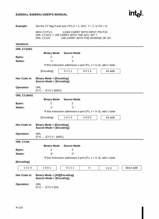
8x930Ax, 8x930Hx USER’S MANUAL
Example: Set the CY flag if and only if P1.0 = 1, ACC. 7 = 1, or OV = 0:
MOV CY,P1.0 ;LOAD CARRY WITH INPUT PIN P10 ORL CY,ACC.7 ;OR CARRY WITH THE ACC. BIT 7 ORL CY,/OV ;OR CARRY WITH THE INVERSE OF OV.
Variations
ORL CY,bit51
Binary Mode Source Mode
Bytes: 2 2
States: 1† 1†
†If this instruction addresses a port (Px, x = 0–3), add 1 state.
Hex Code in: Binary Mode = [Encoding]Source Mode = [Encoding]
Operation: ORL (CY) ← (CY) V (bit51)
ORL CY,/bit51
Binary Mode Source Mode
Bytes: 2 2
States: 1† 1†
†If this instruction addresses a port (Px, x = 0–3), add 1 state.
Hex Code in: Binary Mode = [Encoding]Source Mode = [Encoding]
Operation: ORL (CY) ← (CY) V¬ (bit51)
ORL CY,bit
Binary Mode Source Mode
Bytes: 4 3
States: 3† 2†
†If this instruction addresses a port (Px, x = 0–3), add 1 state.
[Encoding]
Hex Code in: Binary Mode = [A5][Encoding]Source Mode = [Encoding]
Operation: ORL (CY) ← (CY) V (bit)
[Encoding] 0 1 1 1 0 0 1 0 bit addr
[Encoding] 1 0 1 0 0 0 0 0 bit addr
1 0 1 0 1 0 0 1 0 1 1 1 0 y y y direct addr
A-110

INSTRUCTION SET REFERENCE
ORL CY,/bit
Binary Mode Source Mode
Bytes: 4 3
States: 3† 2†
†If this instruction addresses a port (Px, x = 0–3), add 1 state.
[Encoding]
Hex Code in: Binary Mode = [A5][Encoding]Source Mode = [Encoding]
Operation: ORL (CY) ← (CY) V ¬ (bit)
POP <src> Function: Pop from stack
Description: Reads the contents of the on-chip RAM location addressed by the stack pointer, then decrements the stack pointer by one. The value read at the original RAM location is transferred to the newly addressed location, which can be 8-bit or 16-bit.
Flags:
Example: The stack pointer contains 32H and on-chip RAM locations 30H through 32H contain 01H, 23H, and 20H, respectively. After executing the instruction sequence
POP DPH POP DPL
the stack pointer contains 30H and the data pointer contains 0123H. After executing the instruction
POP SP
the stack pointer contains 20H. Note that in this special case the stack pointer was decremented to 2FH before it was loaded with the value popped (20H).
Variations
POP dir8
Binary Mode Source Mode
Bytes: 2 2
States: 3 3
Hex Code in: Binary Mode = [Encoding]Source Mode = [Encoding]
1 0 1 0 1 0 0 1 1 1 1 0 0 y y y direct addr
CY AC OV N Z
— — — — —
[Encoding] 1 1 0 1 0 0 0 0 direct addr
A-111

8x930Ax, 8x930Hx USER’S MANUAL
Operation: POP (dir8) ← ((SP)) (SP) ← (SP) – 1
POP Rm
Bytes: 3 2
States: 3 2
Hex Code in: Binary Mode = [A5][Encoding]Source Mode = [Encoding]
Operation: POP (Rm) ← ((SP)) (SP) ← (SP) – 1
POP WRj
Binary Mode Source Mode
Bytes: 3 2
States: 5 4
Hex Code in: Binary Mode = [A5][Encoding]Source Mode = [Encoding]
Operation: POP (SP) ← (SP) – 1 (WRj) ← ((SP)) (SP) ← (SP) – 1
POP DRk
Binary Mode Source Mode
Bytes: 3 2
States: 10 9
Hex Code in: Binary Mode = [A5][Encoding]Source Mode = [Encoding]
Operation: POP (SP) ← (SP) – 3(DRk) ← ((SP)) (SP) ← (SP) – 1
PUSH <dest>Function: Push onto stack
Description: Increments the stack pointer by one. The contents of the specified variable are then copied into the on-chip RAM location addressed by the stack pointer.
[Encoding] 1 1 0 1 1 0 1 0 s s s s 1 0 0 0
[Encoding] 1 1 0 1 1 0 1 0 t t t t 1 0 0 1
[Encoding] 1 1 0 1 1 0 1 0 u u u u 1 0 1 1
A-112

INSTRUCTION SET REFERENCE
Flags:
Example: On entering an interrupt routine, the stack pointer contains 09H and the data pointer contains 0123H. After executing the instruction sequence
PUSH DPL PUSH DPH
the stack pointer contains 0BH and on-chip RAM locations 0AH and 0BH contain 01H and 23H, respectively.
Variations
PUSH dir8
Binary Mode Source Mode
Bytes: 2 2
States: 4 4
Hex Code in: Binary Mode = [Encoding]Source Mode = [Encoding]
Operation: PUSH (SP) ← (SP) + 1 ((SP)) ← (dir8)
PUSH #data
Binary Mode Source Mode
Bytes: 4 3
States: 4 3
Hex Code in: Binary Mode = [Encoding]Source Mode = [Encoding]
Operation: PUSH (SP) ← (SP) + 1 ((SP)) ← #data
PUSH #data16
Binary Mode Source Mode
Bytes: 5 4
States: 6 5
[Encoding]
Hex Code in: Binary Mode = [A5][Encoding]Source Mode = [Encoding]
CY AC OV N Z
— — — — —
[Encoding] 1 1 0 0 0 0 0 0 direct addr
[Encoding] 1 1 0 0 1 0 1 0 0 0 0 0 0 0 1 0 #data
1 1 0 0 1 0 1 0 0 0 0 0 0 1 1 0 #data hi #data lo
A-113
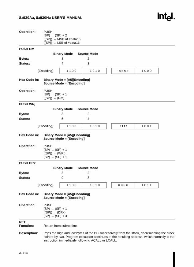
8x930Ax, 8x930Hx USER’S MANUAL
Operation: PUSH(SP) ← (SP) + 2((SP)) ← MSB of #data16 ((SP)) ← LSB of #data16
PUSH Rm
Binary Mode Source Mode
Bytes: 3 2
States: 4 3
Hex Code in: Binary Mode = [A5][Encoding]Source Mode = [Encoding]
Operation: PUSH (SP) ← (SP) + 1 ((SP)) ← (Rm)
PUSH WRj
Binary Mode Source Mode
Bytes: 3 2
States: 5 4
Hex Code in: Binary Mode = [A5][Encoding]Source Mode = [Encoding]
Operation: PUSH (SP) ← (SP) + 1((SP)) ← (WRj) (SP) ← (SP) + 1
PUSH DRk
Binary Mode Source Mode
Bytes: 3 2
States: 9 8
Hex Code in: Binary Mode = [A5][Encoding]Source Mode = [Encoding]
Operation: PUSH (SP) ← (SP) + 1((SP)) ← (DRk) (SP) ← (SP) + 3
RET Function: Return from subroutine Description: Pops the high and low bytes of the PC successively from the stack, decrementing the stack
pointer by two. Program execution continues at the resulting address, which normally is the instruction immediately following ACALL or LCALL.
[Encoding] 1 1 0 0 1 0 1 0 s s s s 1 0 0 0
[Encoding] 1 1 0 0 1 0 1 0 t t t t 1 0 0 1
[Encoding] 1 1 0 0 1 0 1 0 u u u u 1 0 1 1
A-114

INSTRUCTION SET REFERENCE
Flags:
Example: The stack pointer contains 0BH and on-chip RAM locations 0AH and 0BH contain 01H and 23H, respectively. After executing the instruction,
RET
the stack pointer contains 09H and program execution continues at location 0123H.
Binary Mode Source Mode
Bytes: 1 1
States: 7 7
Hex Code in: Binary Mode = [Encoding]Source Mode = [Encoding]
Operation: RET (PC).15:8 ← ((SP)) (SP) ← (SP) – 1 (PC).7:0 ← ((SP)) (SP) ← (SP) – 1
RETI
Function: Return from interrupt
Description: This instruction pops two or four bytes from the stack, depending on the INTR bit in the CONFIG1 register.
If INTR = 0, RETI pops the high and low bytes of the PC successively from the stack and uses them as the 16-bit return address in region FF:. The stack pointer is decremented by two. No other registers are affected, and neither PSW nor PSW1 is automatically restored to its pre-interrupt status.
If INTR = 1, RETI pops four bytes from the stack: PSW1 and the three bytes of the PC. The three bytes of the PC are the return address, which can be anywhere in the 16-Mbyte memory space. The stack pointer is decremented by four. PSW1 is restored to its pre-interrupt status, but PSW is not restored to its pre-interrupt status. No other registers are affected.
For either value of INTR, hardware restores the interrupt logic to accept additional interrupts at the same priority level as the one just processed. Program execution continues at the return address, which normally is the instruction immediately after the point at which the interrupt request was detected. If an interrupt of the same or lower priority is pending when the RETI instruction is executed, that one instruction is executed before the pending interrupt is processed.
Flags:
CY AC OV N Z
— — — — —
[Encoding] 0 0 1 0 0 0 1 0
CY AC OV N Z
— — — — —
A-115
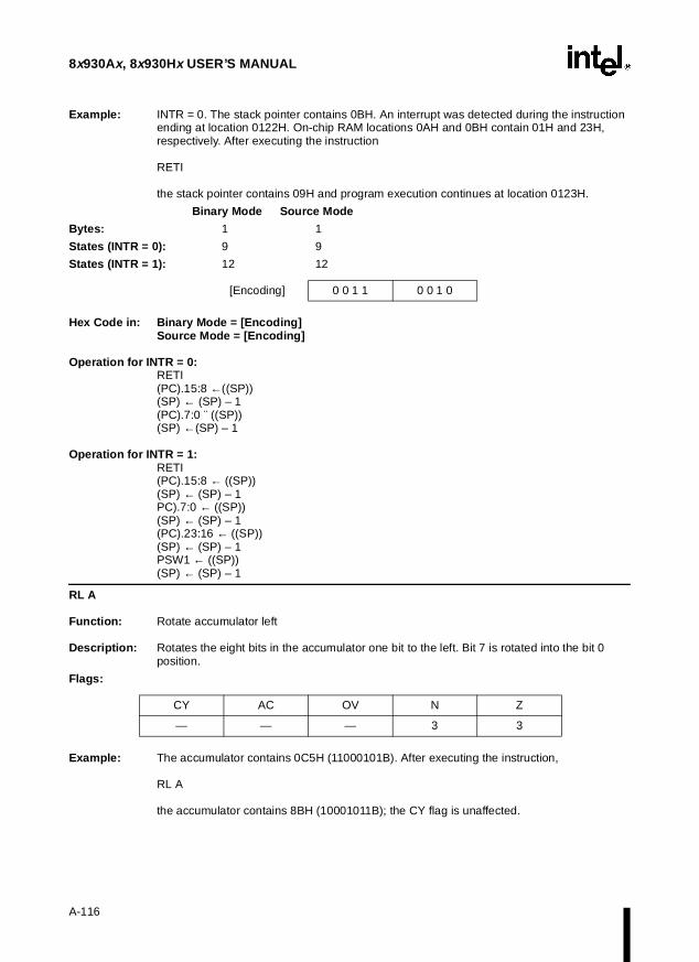
8x930Ax, 8x930Hx USER’S MANUAL
Example: INTR = 0. The stack pointer contains 0BH. An interrupt was detected during the instruction ending at location 0122H. On-chip RAM locations 0AH and 0BH contain 01H and 23H, respectively. After executing the instruction
RETI
the stack pointer contains 09H and program execution continues at location 0123H.
Binary Mode Source Mode
Bytes: 1 1
States (INTR = 0): 9 9
States (INTR = 1): 12 12
Hex Code in: Binary Mode = [Encoding]Source Mode = [Encoding]
Operation for INTR = 0:RETI (PC).15:8 ←((SP))(SP) ← (SP) – 1(PC).7:0 ¨ ((SP)) (SP) ←(SP) – 1
Operation for INTR = 1:RETI(PC).15:8 ← ((SP))(SP) ← (SP) – 1 PC).7:0 ← ((SP)) (SP) ← (SP) – 1 (PC).23:16 ← ((SP))(SP) ← (SP) – 1 PSW1 ← ((SP))(SP) ← (SP) – 1
RL A
Function: Rotate accumulator left
Description: Rotates the eight bits in the accumulator one bit to the left. Bit 7 is rotated into the bit 0 position.
Flags:
Example: The accumulator contains 0C5H (11000101B). After executing the instruction,
RL A
the accumulator contains 8BH (10001011B); the CY flag is unaffected.
[Encoding] 0 0 1 1 0 0 1 0
CY AC OV N Z
— — — 3 3
A-116

INSTRUCTION SET REFERENCE
Binary Mode Source Mode
Bytes: 1 1
States: 1 1
Hex Code in: Binary Mode = [Encoding]Source Mode = [Encoding]
Operation: RL (A).a+1 ← (A).a(A).0 ← (A).7
RLC A
Function: Rotate accumulator left through the carry flag
Description: Rotates the eight bits in the accumulator and the CY flag one bit to the left. Bit 7 moves into the CY flag position and the original state of the CY flag moves into bit 0 position.
Flags:
Example: The accumulator contains 0C5H (11000101B) and the CY flag is clear. After executing the instruction
RLC A
the accumulator contains 8AH (10001010B) and the CY flag is set.
Binary Mode Source Mode
Bytes: 1 1
States: 1 1
Hex Code in: Binary Mode = [Encoding]Source Mode = [Encoding]
Operation: RLC (A).a+1 ← (A).a(A).0 ← (CY) (CY) ← (A).7
RR A
Function: Rotate accumulator right
Description: Rotates the 8 or 16 bits in the accumulator one bit to the right. Bit 0 is moved into the bit 7 or 15 position.
Flags:
[Encoding] 0 0 1 0 0 0 1 1
CY AC OV N Z
3 — — 3 3
[Encoding] 0 0 1 1 0 0 1 1
CY AC OV N Z
— — — 3 3
A-117

8x930Ax, 8x930Hx USER’S MANUAL
Example: The accumulator contains 0C5H (11000101B). After executing the instruction
RR A
the accumulator contains 0E2H (11100010B) and the CY flag is unaffected.
Binary Mode Source Mode
Bytes: 1 1
States: 1 1
Hex Code in: Binary Mode = [Encoding]Source Mode = [Encoding]
Operation: RR (A).a ← (A).a+1(A).7 ← (A) .0
RRC A
Function: Rotate accumulator right through carry flag
Description: Rotates the eight bits in the accumulator and the CY flag one bit to the right. Bit 0 moves into the CY flag position; the original value of the CY flag moves into the bit 7 position.
Flags:
Example: The accumulator contains 0C5H (11000101B) and the CY flag is clear. After executing the instruction
RRC A
the accumulator contains 62 (01100010B) and the CY flag is set.
Binary Mode Source Mode
Bytes: 1 1
States: 1 1
Hex Code in: Binary Mode = [Encoding]Source Mode = [Encoding]
Operation: RRC (A).a ← (A).a+1(A).7 ← (CY) (CY) ← (A).0
SETB <bit> Function: Set bit
[Encoding] 0 0 0 0 0 0 1 1
CY AC OV N Z
3 — — 3 3
[Encoding] 0 0 0 1 0 0 1 1
A-118

INSTRUCTION SET REFERENCE
Description: Sets the specified bit to one. SETB can operate on the CY flag or any directly addressable bit.
Flags: No flags are affected except the CY flag for instruction with CY as the operand.
Example: The CY flag is clear and output Port 1 contains 34H (00110100B). After executing the instruction sequence
SETB CY SETB P1.0
the CY flag is set and output Port 1 contains 35H (00110101B).
SETB bit51
Binary Mode Source Mode
Bytes: 2 2
States: 2† 2†
†If this instruction addresses a port (Px, x = 0–3), add 2 states.
Hex Code in: Binary Mode = [Encoding]Source Mode = [Encoding]
Operation: SETB (bit51) ← 1
SETB CY
Binary Mode Source Mode
Bytes: 1 1
States: 1 1
Hex Code in: Binary Mode = [Encoding]Source Mode = [Encoding]
Operation: SETB (CY) ← 1
SETB bit
Binary Mode Source Mode
Bytes: 4 3
States: 4† 3†
†If this instruction addresses a port (Px, x = 0–3), add 2 states.
[Encoding]
CY AC OV N Z
3 — — — —
[Encoding] 1 1 0 1 0 0 1 0 bit addr
[Encoding] 1 1 0 1 0 0 1 1
1 0 1 0 1 0 0 1 1 1 0 1 0 y y y direct addr
A-119
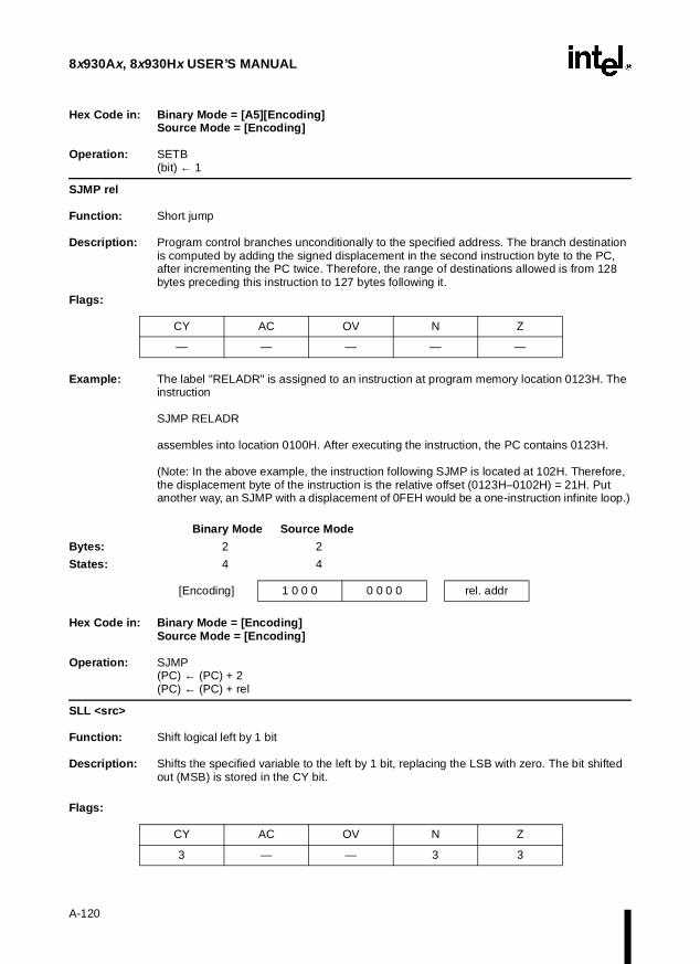
8x930Ax, 8x930Hx USER’S MANUAL
Hex Code in: Binary Mode = [A5][Encoding]Source Mode = [Encoding]
Operation: SETB (bit) ← 1
SJMP rel
Function: Short jump
Description: Program control branches unconditionally to the specified address. The branch destination is computed by adding the signed displacement in the second instruction byte to the PC, after incrementing the PC twice. Therefore, the range of destinations allowed is from 128 bytes preceding this instruction to 127 bytes following it.
Flags:
Example: The label "RELADR" is assigned to an instruction at program memory location 0123H. The instruction
SJMP RELADR
assembles into location 0100H. After executing the instruction, the PC contains 0123H.
(Note: In the above example, the instruction following SJMP is located at 102H. Therefore, the displacement byte of the instruction is the relative offset (0123H–0102H) = 21H. Put another way, an SJMP with a displacement of 0FEH would be a one-instruction infinite loop.)
Binary Mode Source Mode
Bytes: 2 2
States: 4 4
Hex Code in: Binary Mode = [Encoding]Source Mode = [Encoding]
Operation: SJMP (PC) ← (PC) + 2 (PC) ← (PC) + rel
SLL <src>
Function: Shift logical left by 1 bit
Description: Shifts the specified variable to the left by 1 bit, replacing the LSB with zero. The bit shifted out (MSB) is stored in the CY bit.
Flags:
CY AC OV N Z
— — — — —
[Encoding] 1 0 0 0 0 0 0 0 rel. addr
CY AC OV N Z
3 — — 3 3
A-120

INSTRUCTION SET REFERENCE
Example: Register 1 contains 0C5H (11000101B). After executing the instruction
SLL register 1
Register 1 contains 8AH (10001010B) and CY = 1.Variations
SLL Rm
Binary Mode Source Mode
Bytes: 3 2
States: 2 1
Hex Code in: Binary Mode = [A5][Encoding]Source Mode = [Encoding]
Operation: SLL(Rm).a+1 ← (Rm).a (Rm).0 ← 0 CY ← (Rm).7
SLL WRj
Binary Mode Source Mode
Bytes: 3 2
States: 2 1
Hex Code in: Binary Mode = [A5][Encoding]Source Mode = [Encoding]
Operation: SLLWRj).b+1 ← (WRj).b (WRj).0 ← 0 CY← (WRj).15
SRA <src>
Function: Shift arithmetic right by 1 bit
Description: Shifts the specified variable to the arithmetic right by 1 bit. The MSB is unchanged. The bit shifted out (LSB) is stored in the CY bit.
Flags:
[Encoding] 0 0 1 1 1 1 1 0 s s s s 0 0 0 0
[Encoding] 0 0 1 1 1 1 1 0 t t t t 0 1 0 0
CY AC OV N Z
3 — — 3 3
A-121

8x930Ax, 8x930Hx USER’S MANUAL
Example: Register 1 contains 0C5H (11000101B). After executing the instruction
SRA register 1
Register 1 contains 0E2H (11100010B) and CY = 1.Variations
SRA Rm
Binary Mode Source Mode
Bytes: 3 2
States: 2 1
Hex Code in: Binary Mode = [A5][Encoding]Source Mode = [Encoding]
Operation: SRA(Rm).7 ← (Rm).7 (Rm).a ← (Rm).a+1 CY← (Rm).0
SRA WRj
Binary Mode Source Mode
Bytes: 3 2
States: 2 1
Hex Code in: Binary Mode = [A5][Encoding]Source Mode = [Encoding]
Operation: SRA(WRj).15 ← (WRj).15 (WRj).b ← (WRj).b+1 CY← (WRj).0
SRL <src>
Function: Shift logical right by 1 bit
Description: SRL shifts the specified variable to the right by 1 bit, replacing the MSB with a zero. The bit shifted out (LSB) is stored in the CY bit.
Flags:
Example: Register 1 contains 0C5H (11000101B). After executing the instruction
SRL register 1
Register 1 contains 62H (01100010B) and CY = 1.
[Encoding] 0 0 0 0 1 1 1 0 s s s s 0 0 0 0
[Encoding] 0 0 0 0 1 1 1 0 t t t t 0 1 0 0
CY AC OV N Z
3 — — 3 3
A-122

INSTRUCTION SET REFERENCE
SRL Rm
Binary Mode Source Mode
Bytes: 3 2
States: 2 1
Hex Code in: Binary Mode = [A5][Encoding]Source Mode = [Encoding]
Operation: SRL(Rm).7 ← 0(Rm).a ← (Rm).a+1CY← (Rm).0
SRL WRj
Binary Mode Source Mode
Bytes: 3 2
States: 2 1
Hex Code in: Binary Mode = [A5][Encoding]Source Mode = [Encoding]
Operation: SRL(WRj).15 ← 0(WRj).b ← (WRj).b+1 CY← (WRj).0
SUB <dest>,<src>
Function: Subtract
Description: Subtracts the specified variable from the destination operand, leaving the result in the destination operand. SUB sets the CY (borrow) flag if a borrow is needed for bit 7. Otherwise, CY is clear.
When subtracting signed integers, the OV flag indicates a negative number produced when a negative value is subtracted from a positive value, or a positive result when a positive number is subtracted from a negative number.
Bit 7 in this description refers to the most significant byte of the operand (8, 16, or 32 bit).
The source operand allows four addressing modes: immediate, indirect, register and direct.
Flags:
†For word and dword subtractions, AC is not affected.
[Encoding] 0 0 0 1 1 1 1 0 s s s s 0 0 0 0
[Encoding] 0 0 0 1 1 1 1 0 t t t t 0 1 0 0
CY AC OV N Z
3 † 3 3 3
A-123
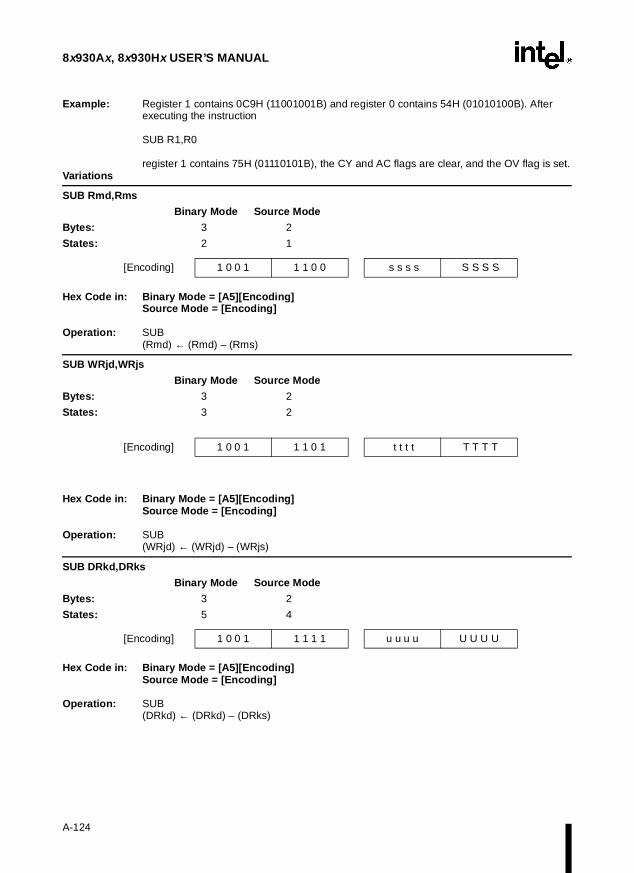
8x930Ax, 8x930Hx USER’S MANUAL
Example: Register 1 contains 0C9H (11001001B) and register 0 contains 54H (01010100B). After executing the instruction
SUB R1,R0
register 1 contains 75H (01110101B), the CY and AC flags are clear, and the OV flag is set. Variations
SUB Rmd,Rms
Binary Mode Source Mode
Bytes: 3 2
States: 2 1
Hex Code in: Binary Mode = [A5][Encoding]Source Mode = [Encoding]
Operation: SUB(Rmd) ← (Rmd) – (Rms)
SUB WRjd,WRjs
Binary Mode Source Mode
Bytes: 3 2
States: 3 2
Hex Code in: Binary Mode = [A5][Encoding]Source Mode = [Encoding]
Operation: SUB(WRjd) ← (WRjd) – (WRjs)
SUB DRkd,DRks
Binary Mode Source Mode
Bytes: 3 2
States: 5 4
Hex Code in: Binary Mode = [A5][Encoding]Source Mode = [Encoding]
Operation: SUB(DRkd) ← (DRkd) – (DRks)
[Encoding] 1 0 0 1 1 1 0 0 s s s s S S S S
[Encoding] 1 0 0 1 1 1 0 1 t t t t T T T T
[Encoding] 1 0 0 1 1 1 1 1 u u u u U U U U
A-124

INSTRUCTION SET REFERENCE
SUB Rm,#data
Binary Mode Source Mode
Bytes: 4 3
States: 3 2
Hex Code in: Binary Mode = [A5][Encoding]Source Mode = [Encoding]
Operation: SUB (Rm) ← (Rm) – #data
SUB WRj,#data16
Binary Mode Source Mode
Bytes: 5 4
States: 4 3
[Encoding]
Hex Code in: Binary Mode = [A5][Encoding]Source Mode = [Encoding]
Operation: SUB (WRj) ← (WRj) – #data16
SUB DRk,#data16
Binary Mode Source Mode
Bytes: 5 4
States: 6 5
[Encoding]
Hex Code in: Binary Mode = [A5][Encoding]Source Mode = [Encoding]
Operation: SUB (DRk) ← (DRk) – #data16
SUB Rm,dir8
Binary Mode Source Mode
Bytes: 4 3
States: 3† 2†
†If this instruction addresses a port (Px, x = 0–3), add 1 state.
Hex Code in: Binary Mode = [A5][Encoding]Source Mode = [Encoding]
[Encoding] 1 0 0 1 1 1 1 0 s s s s 0 0 0 0 #data
1 0 0 1 1 1 1 0 t t t t 0 1 0 0 #data hi #data low
1 0 0 1 1 1 1 0 u u u u 1 0 0 0 #data hi #data low
[Encoding] 1 0 0 1 1 1 1 0 s s s s 0 0 0 1 direct addr
A-125

8x930Ax, 8x930Hx USER’S MANUAL
Operation: SUB (Rm) ← (Rm) – (dir8)
SUB WRj,dir8
Binary Mode Source Mode
Bytes: 4 3
States: 4 3
Hex Code in: Binary Mode = [A5][Encoding]Source Mode = [Encoding]
Operation: SUB (WRj) ← (WRj) – (dir8)
SUB Rm,dir16
Binary Mode Source Mode
Bytes: 5 4
States: 3 2
[Encoding]
Hex Code in: Binary Mode = [A5][Encoding]Source Mode = [Encoding]
Operation: SUB (Rm) ← (Rm) – (dir16)
SUB WRj,dir16
Binary Mode Source Mode
Bytes: 5 4
States: 4 3
[Encoding]
Hex Code in: Binary Mode = [A5][Encoding]Source Mode = [Encoding]
Operation: SUB (WRj) ← (WRj) – (dir16)
SUB Rm,@WRj
Binary Mode Source Mode
Bytes: 4 3
States: 3 2
[Encoding]
[Encoding] 1 0 0 1 1 1 1 0 t t t t 0 1 0 1 direct addr
1 0 0 1 1 1 1 0 s s s s 0 0 1 1 direct addr direct addr
1 0 0 1 1 1 1 0 t t t t 0 1 1 1 direct addr direct addr
1 0 0 1 1 1 1 0 t t t t 1 0 0 1 s s s s 0 0 0 0
A-126

INSTRUCTION SET REFERENCE
Hex Code in: Binary Mode = [A5][Encoding]Source Mode = [Encoding]
Operation: SUB (Rm) ← (Rm) – ((WRj))
SUB Rm,@DRk
Binary Mode Source Mode
Bytes: 4 3
States: 4 3
[Encoding]
Hex Code in: Binary Mode = [A5][Encoding]Source Mode = [Encoding]
Operation: SUB (Rm) ← (Rm) – ((DRk))
SUBB A,<src–byte> Function: Subtract with borrow
Description: SUBB subtracts the specified variable and the CY flag together from the accumulator, leaving the result in the accumulator. SUBB sets the CY (borrow) flag if a borrow is needed for bit 7, and clears CY otherwise. (If CY was set before executing a SUBB instruction, this indicates that a borrow was needed for the previous step in a multiple precision subtraction, so the CY flag is subtracted from the accumulator along with the source operand.) AC is set if a borrow is needed for bit 3, and cleared otherwise. OV is set if a borrow is needed into bit 6, but not into bit 7, or into bit 7, but not bit 6.
When subtracting signed integers the OV flag indicates a negative number produced when a negative value is subtracted from a positive value, or a positive result when a positive number is subtracted from a negative number.
Bit 6 and bit 7 in this description refer to the most significant byte of the operand (8, 16, or 32 bit).
The source operand allows four addressing modes: register, direct, register-indirect, or immediate.
Flags:
Example: The accumulator contains 0C9H (11001001B), register 2 contains 54H (01010100B), and the CY flag is set. After executing the instruction
SUBB A,R2
the accumulator contains 74H (01110100B), the CY and AC flags are clear, and the OV flag is set.
1 0 0 1 1 1 1 0 u u u u 1 0 1 1 s s s s 0 0 0 0
CY AC OV N Z
3 3 3 3 3
A-127
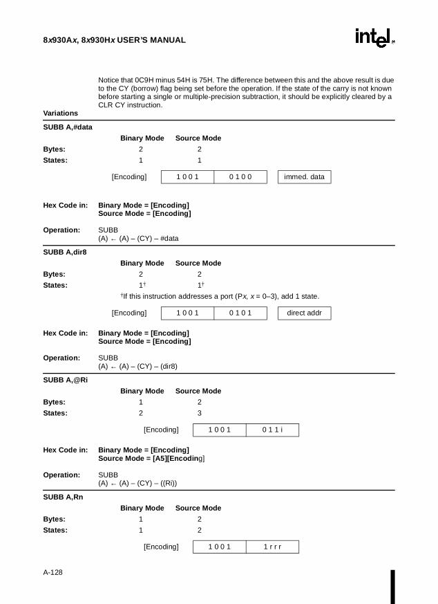
8x930Ax, 8x930Hx USER’S MANUAL
Notice that 0C9H minus 54H is 75H. The difference between this and the above result is due to the CY (borrow) flag being set before the operation. If the state of the carry is not known before starting a single or multiple-precision subtraction, it should be explicitly cleared by a CLR CY instruction.
Variations
SUBB A,#data
Binary Mode Source Mode
Bytes: 2 2
States: 1 1
Hex Code in: Binary Mode = [Encoding]Source Mode = [Encoding]
Operation: SUBB (A) ← (A) – (CY) – #data
SUBB A,dir8
Binary Mode Source Mode
Bytes: 2 2
States: 1† 1†
†If this instruction addresses a port (Px, x = 0–3), add 1 state.
Hex Code in: Binary Mode = [Encoding]Source Mode = [Encoding]
Operation: SUBB (A) ← (A) – (CY) – (dir8)
SUBB A,@Ri
Binary Mode Source Mode
Bytes: 1 2
States: 2 3
Hex Code in: Binary Mode = [Encoding]Source Mode = [A5][Encodin g]
Operation: SUBB (A) ← (A) – (CY) – ((Ri))
SUBB A,Rn
Binary Mode Source Mode
Bytes: 1 2
States: 1 2
[Encoding] 1 0 0 1 0 1 0 0 immed. data
[Encoding] 1 0 0 1 0 1 0 1 direct addr
[Encoding] 1 0 0 1 0 1 1 i
[Encoding] 1 0 0 1 1 r r r
A-128

INSTRUCTION SET REFERENCE
Hex Code in: Binary Mode = [Encoding]Source Mode = [A5][Encodin g]
Operation: SUBB (A) ← (A) – (CY) – (Rn)
SWAP A
Function: Swap nibbles within the accumulator
Description: Interchanges the low and high nibbles (4-bit fields) of the accumulator (bits 3–0 and bits 7–4). This operation can also be thought of as a 4-bit rotate instruction.
Flags:
Example: The accumulator contains 0C5H (11000101B). After executing the instruction
SWAP A
the accumulator contains 5CH (01011100B).
Binary Mode Source Mode
Bytes: 1 1
States: 2 2
Hex Code in: Binary Mode = [Encoding]Source Mode = [Encoding]
Operation: SWAP (A).3:0 → ← (A).7:4
TRAP Function: Causes interrupt call
Description: Causes an interrupt call that is vectored through location 0FF007BH. The operation of this instruction is not affected by the state of the interrupt enable flag in PSW0 and PSW1. Interrupt calls can not occur immediately following this instruction. This instruction is intended for use by Intel-provided development tools. These tools do not support user application of this instruction.
Flags:
Example: The instruction
TRAP
causes an interrupt call to location 0FF007BH during normal operation.
CY AC OV N Z
— — — — —
[Encoding] 1 1 0 0 0 1 0 0
CY AC OV N Z
— — — — —
A-129

8x930Ax, 8x930Hx USER’S MANUAL
Binary Mode Source Mode
Bytes: 2 1
States (2 bytes): 11 10
States (4 bytes): 16 15
Hex Code in: Binary Mode = [A5][Encoding]Source Mode = [Encoding]
Operation: TRAPSP ← SP – 2(SP) ← PCPC ← (0FF007BH)
XCH A,<byte>
Function: Exchange accumulator with byte variable Description: Loads the accumulator with the contents of the specified variable, at the same time writing
the original accumulator contents to the specified variable. The source/destination operand can use register, direct, or register-indirect addressing.
Flags:
Example: R0 contains the address 20H, the accumulator contains 3FH (00111111B) and on-chip RAM location 20H contains 75H (01110101B). After executing the instruction
XCH A,@R0
RAM location 20H contains 3FH (00111111B) and the accumulator contains 75H (01110101B).
Variations
XCH A,dir8
Binary Mode Source Mode
Bytes: 2 2
States: 3† 3†
†f this instruction addresses a port (Px, x = 0–3), add 2 states.
Hex Code in: Binary Mode = [Encoding]Source Mode = [Encoding]
Operation: XCH (A) → ← (dir8)
[Encoding] 1 0 1 1 1 0 0 1
CY AC OV N Z
— — — — —
[Encoding] 1 1 0 0 0 1 0 1 direct addr
A-130
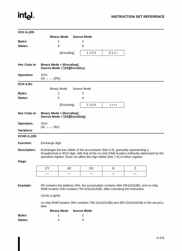
INSTRUCTION SET REFERENCE
XCH A,@Ri
Binary Mode Source Mode
Bytes: 1 2
States: 4 5
Hex Code in: Binary Mode = [Encoding]Source Mode = [A5][Encodin g]
Operation: XCH (A) → ← ((Ri))
XCH A,Rn
Binary Mode Source Mode
Bytes: 1 2
States: 3 4
Hex Code in: Binary Mode = [Encoding]Source Mode = [A5][Encoding]
Operation: XCH (A) → ← (Rn)
Variations
XCHD A,@Ri
Function: Exchange digit Description: Exchanges the low nibble of the accumulator (bits 3-0), generally representing a
hexadecimal or BCD digit, with that of the on-chip RAM location indirectly addressed by the specified register. Does not affect the high nibble (bits 7-4) of either register.
Flags:
Example: R0 contains the address 20H, the accumulator contains 36H (00110110B), and on-chip RAM location 20H contains 75H (01110101B). After executing the instruction
XCHD A,@R0
on-chip RAM location 20H contains 76H (01110110B) and 35H (00110101B) in the accumu-lator.
Binary Mode Source Mode
Bytes: 1 2
States: 4 5
[Encoding] 1 1 0 0 0 1 1 i
[Encoding] 1 1 0 0 1 r r r
CY AC OV N Z
— — — — —
A-131

8x930Ax, 8x930Hx USER’S MANUAL
Hex Code in: Binary Mode = [Encoding]Source Mode = [Encoding]
Operation: XCHD (A).3:0 → ← ((Ri)).3:0
XRL <dest>,<src> Function: Logical Exclusive-OR for byte variables Description: Performs the bitwise logical Exclusive-OR operation (∀) between the specified variables,
storing the results in the destination. The destination operand can be the accumulator, a register, or a direct address.
The two operands allow 12 addressing mode combinations. When the destination is the accumulator or a register, the source addressing can be register, direct, register-indirect, or immediate; when the destination is a direct address, the source can be the accumulator or immediate data.
(Note: When this instruction is used to modify an output port, the value used as the original port data is read from the output data latch, not the input pins.)
Flags:
Example: The accumulator contains 0C3H (11000011B) and R0 contains 0AAH (10101010B). After executing the instruction
XRL A,R0
the accumulator contains 69H (01101001B).
When the destination is a directly addressed byte, this instruction can complement combina-tions of bits in any RAM location or hardware register. The pattern of bits to be comple-mented is then determined by a mask byte, either a constant contained in the instruction or a variable computed in the accumulator at run time. The instruction
XRL P1,#00110001B
complements bits 5, 4, and 0 of output Port 1. Variations
XRL dir8,A
Binary Mode Source Mode
Bytes: 2 2
States: 2† 2†
†If this instruction addresses a port (Px, x = 0–3), add 2 states.
[Encoding] 1 1 0 1 0 1 1 i
CY AC OV N Z
— — — 3 3
[Encoding] 0 1 1 0 0 0 1 0 direct addr
A-132

INSTRUCTION SET REFERENCE
Hex Code in: Binary Mode = [Encoding]Source Mode = [Encoding]
Operation: XRL (dir8) ← (dir8) ∀ (A)
XRL dir8,#data
Binary Mode Source Mode
Bytes: 3 3
States: 3† 3†
†If this instruction addresses a port (Px, x = 0–3), add 1 state.
Hex Code in: Binary Mode = [Encoding]Source Mode = [Encoding]
Operation: XRL (dir8) ← (dir8) ∀ #data
XRL A,#data
Binary Mode Source Mode
Bytes: 2 2
States: 1 1
Hex Code in: Binary Mode = [Encoding]Source Mode = [Encoding]
Operation: XRL (A) ← (A) ∀ #data
XRL A,dir8
Binary Mode Source Mode
Bytes: 2 2
States: 1† 1†
†If this instruction addresses a port (Px, x = 0–3), add 1 state.
Hex Code in: Binary Mode = [Encoding]Source Mode = [Encoding]
Operation: XRL (A) ← (A) ∀ (dir8)
XRL A,@Ri
Binary Mode Source Mode
Bytes: 1 2
States: 2 3
[Encoding] 0 1 1 0 0 0 1 1 direct addr immed. data
[Encoding] 0 1 1 0 0 1 0 0 immed. data
[Encoding] 0 1 1 0 0 1 0 1 direct addr
A-133
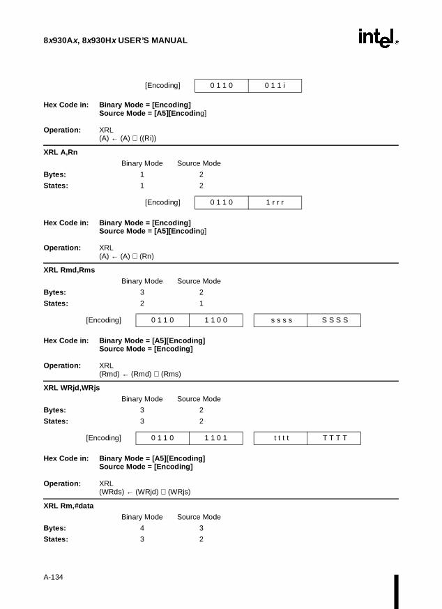
8x930Ax, 8x930Hx USER’S MANUAL
Hex Code in: Binary Mode = [Encoding]Source Mode = [A5][Encodin g]
Operation: XRL (A) ← (A) ∀ ((Ri))
XRL A,Rn
Binary Mode Source Mode
Bytes: 1 2
States: 1 2
Hex Code in: Binary Mode = [Encoding]Source Mode = [A5][Encodin g]
Operation: XRL (A) ← (A) ∀ (Rn)
XRL Rmd,Rms
Binary Mode Source Mode
Bytes: 3 2
States: 2 1
Hex Code in: Binary Mode = [A5][Encoding]Source Mode = [Encoding]
Operation: XRL (Rmd) ← (Rmd) ∀ (Rms)
XRL WRjd,WRjs
Binary Mode Source Mode
Bytes: 3 2
States: 3 2
Hex Code in: Binary Mode = [A5][Encoding]Source Mode = [Encoding]
Operation: XRL (WRds) ← (WRjd) ∀ (WRjs)
XRL Rm,#data
Binary Mode Source Mode
Bytes: 4 3
States: 3 2
[Encoding] 0 1 1 0 0 1 1 i
[Encoding] 0 1 1 0 1 r r r
[Encoding] 0 1 1 0 1 1 0 0 s s s s S S S S
[Encoding] 0 1 1 0 1 1 0 1 t t t t T T T T
A-134

INSTRUCTION SET REFERENCE
Hex Code in: Binary Mode = [A5][Encoding]Source Mode = [Encoding]
Operation: XRL (Rm) ← (Rm) ∀ #data
XRL WRj,#data16
Binary Mode Source Mode
Bytes: 5 4
States: 4 3
[Encoding]
Hex Code in: Binary Mode = [A5][Encoding]Source Mode = [Encoding]
Operation: XRL (WRj) ← (WRj) ∀ #data16
XRL Rm,dir8
Binary Mode Source Mode
Bytes: 4 3
States: 3† 2†
†If this instruction addresses a port (Px, x = 0–3), add 1 state.
Hex Code in: Binary Mode = [A5][Encoding]Source Mode = [Encoding]
Operation: XRL (Rm) ← (Rm) ∀ (dir8)
XRL WRj,dir8
Binary Mode Source Mode
Bytes: 4 3
States: 4 3
Hex Code in: Binary Mode = [A5][Encoding]Source Mode = [Encoding]
Operation: XRL (WRj) ← (WRj) ∀ (dir8)
[Encoding] 0 1 1 0 1 1 1 0 s s s s 0 0 0 0 #data
0 1 1 0 1 1 1 0 t t t t 0 1 0 0 #data hi #data low
[Encoding] 0 1 1 0 1 1 1 0 s s s s 0 0 0 1 direct addr
[Encoding] 0 1 1 0 1 1 1 0 t t t t 0 1 0 1 direct addr
A-135

8x930Ax, 8x930Hx USER’S MANUAL
XRL Rm,dir16
Binary Mode Source Mode
Bytes: 5 4
States: 3 2
[Encoding]
Hex Code in: Binary Mode = [A5][Encoding]Source Mode = [Encoding]
Operation: XRL (Rm) ← (Rm) ∀ (dir16)
\XRL WRj,dir16
Binary Mode Source Mode
Bytes: 5 4
States: 4 3
[Encoding]
Hex Code in: Binary Mode = [A5][Encoding]Source Mode = [Encoding]
Operation: XRL (WRj) ← (WRj) ∀ (dir16)
XRL Rm,@Wrj
Binary Mode Source Mode
Bytes: 4 3
States: 3 2
[Encoding]
Hex Code in: Binary Mode = [A5][Encoding]Source Mode = [Encoding]
Operation: XRL (Rm) ← (Rm) ∀ ((WRj))
XRL Rm,@Drk
Binary Mode Source Mode
Bytes: 4 3
States: 4 3
[Encoding]
0 1 1 0 1 1 1 0 s s s s 0 0 1 1 direct addr dir8 addr
0 1 1 0 1 1 1 0 t t t t 0 1 1 1 direct addr direct addr
0 1 1 0 1 1 1 0 t t t t 1 0 0 1 s s s s 0 0 0 0
0 1 1 0 1 1 1 0 u u u u 1 0 1 1 s s s s 0 0 0 0
A-136

INSTRUCTION SET REFERENCE
Hex Code In: Binary Mode = [A5][Encoding]Source Mode = [Encoding]
Operation: XRL(Rm) ← (Rm) ∀ ((DRk))
A-137


BSignal Descriptions


o
xter-
APPENDIX BSIGNAL DESCRIPTIONS
This appendix provides reference information for the external signals of the 8x930. Pin assign-ments for the device are shown in Figure B-1 (8x930Ax) and Figure B-2 (8x930Hx) and are listedby functional category in Table B-1.
Table B-2 describes each of the signals. It lists the signal type (input, output, power, or grund)and the alternative functions of multi-function pins. Table B-3 shows how configuration bitsRD1:0 (referred to in Table B-2) configure the A17, A16, RD#, WR# and PSEN# pins for enal memory accesses.
Figure B-1. 8 x930Ax 68-pin PLCC Package
Reserved Reserved Reserved Reserved Reserved DP0 DM0 ECAP VSSP VCCP SOF# Reserved Reserved Reserved Reserved Reserved PLLSEL0
A8
/ P2.
0 A
9 / P
2.1
A10
/ P
2.2
A11
/ P
2.3
A12
/ P
2.4
A13
/ P
2.5
A14
/ P
2.6
A15
/ P
2.7
VS
S
VC
C
EA
# A
LE
PS
EN
# R
eser
ved
Res
erve
d R
eser
ved
Res
erve
d
A4392-02
AD7 / P0.7 AD6 / P0.6 AD5 / P0.5 AD4 / P0.4 AD3 / P0.3 AD2 / P0.2 AD1 / P0.1 AD0 / P0.0
VSSP VCCP
P3.0 / RXD P3.1 / TXD
P3.2 / INT0# P3.3 / INT1#
P3.4 / T0 P3.5 / T1
P3.6 / WR#
60 59 58 57 56 55 54 53 52 51 50 49 48 47 46 45 44
View of component as mounted on PC board
10 11 12 13 14 15 16 17 18 19 20 21 22 23 24 25 26
P3.
7 / R
D#
/ A16
P
1.0
/ T2
P1.
1 / T
2EX
P
1.2
/ EC
I P
1.3
/ CE
X0
P1.
4 / C
EX
1 P
1.5
/ CE
X2
P1.
6 / C
EX
3 / W
AIT
# P
1.7
/ C
EX
4 / A
17 /
WC
LK
VC
C
VS
S
XT
AL1
X
TA
L2
AV
CC
R
ST
P
LLS
EL1
P
LLS
EL2
27
28
29
30
31
32
33
34
35
36
37
38
39
40
41
42
43
9 8 7 6 5 4 3 2 1 68
67
66
65
64
63
62
61
Note: Reserved pins must be left unconnected.
B-1

8x930Ax, 8x930Hx USER’S MANUAL
Figure B-2. 8 x930Hx 68-pin PLCC Package
UPWEN# OVRI# DP1 DM1 Reserved DP0 DM0 ECAP VSSP VCCP SOF# DP3 DM3 Reserved DP2 DM2 PLLSEL0
A8
/ P2.
0 A
9 / P
2.1
A10
/ P
2.2
A11
/ P
2.3
A12
/ P
2.4
A13
/ P
2.5
A14
/ P
2.6
A15
/ P
2.7
VS
S
VC
C
EA
# A
LE
PS
EN
# R
eser
ved
Res
erve
d R
eser
ved
Res
erve
d
A4375-02
AD7 / P0.7 AD6 / P0.6 AD5 / P0.5 AD4 / P0.4 AD3 / P0.3 AD2 / P0.2 AD1 / P0.1 AD0 / P0.0
VSSP VCCP
P3.0 / RXD P3.1 / TXD
P3.2 / INT0# P3.3 / INT1#
P3.4 / T0 P3.5 / T1
P3.6 / WR#
60 59 58 57 56 55 54 53 52 51 50 49 48 47 46 45 44
View of component as mounted on PC board
10 11 12 13 14 15 16 17 18 19 20 21 22 23 24 25 26
P3.
7 / R
D#
/ A16
P
1.0
/ T2
P1.
1 / T
2EX
P
1.2
/ EC
I P
1.3
/ CE
X0
P1.
4 / C
EX
1 P
1.5
/ CE
X2
P1.
6 / C
EX
3 / W
AIT
# P
1.7
/ CE
X4
/ A17
/ W
CLK
V
CC
V
SS
X
TA
L1
XT
AL2
A
VC
C
RS
T
PLL
SE
L1
PLL
SE
L2
27
28
29
30
31
32
33
34
35
36
37
38
39
40
41
42
43
9 8 7 6 5 4 3 2 1 68
67
66
65
64
63
62
61
Note: Reserved pins must be left unconnected.
B-2
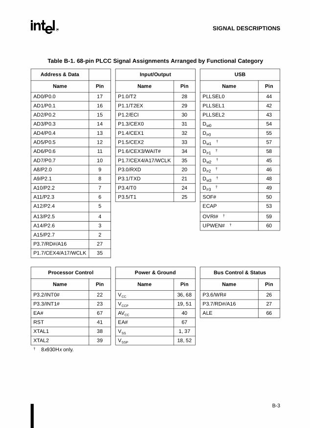
SIGNAL DESCRIPTIONS
Table B-1. 68-pin PLCC Signal Assignments Arranged by Functional Category
Address & Data Input/Output USB
Name Pin Name Pin Name Pin
AD0/P0.0 17 P1.0/T2 28 PLLSEL0 44
AD1/P0.1 16 P1.1/T2EX 29 PLLSEL1 42
AD2/P0.2 15 P1.2/ECI 30 PLLSEL2 43
AD3/P0.3 14 P1.3/CEX0 31 DM0 54
AD4/P0.4 13 P1.4/CEX1 32 DP0 55
AD5/P0.5 12 P1.5/CEX2 33 DM1 † 57
AD6/P0.6 11 P1.6/CEX3/WAIT# 34 DP1 † 58
AD7/P0.7 10 P1.7/CEX4/A17/WCLK 35 DM2 † 45
A8/P2.0 9 P3.0/RXD 20 DP2 † 46
A9/P2.1 8 P3.1/TXD 21 DM3 † 48
A10/P2.2 7 P3.4/T0 24 DP3 † 49
A11/P2.3 6 P3.5/T1 25 SOF# 50
A12/P2.4 5 ECAP 53
A13/P2.5 4 OVRI# † 59
A14/P2.6 3 UPWEN# † 60
A15/P2.7 2
P3.7/RD#/A16 27
P1.7/CEX4/A17/WCLK 35
Processor Control Power & Ground Bus Control & Status
Name Pin Name Pin Name Pin
P3.2/INT0# 22 VCC 36, 68 P3.6/WR# 26
P3.3/INT1# 23 VCCP 19, 51 P3.7/RD#/A16 27
EA# 67 AVCC 40 ALE 66
RST 41 EA# 67
XTAL1 38 VSS 1, 37
XTAL2 39 VSSP 18, 52
† 8x930Hx only.
B-3

8x930Ax, 8x930Hx USER’S MANUAL
Table B-2. Signal Descriptions
Signal Name Type Description Alternate
Function
A17 O Address Line 17. Output to memory as 18th external address bit in extended bus applications. Selected with bits RD1:0 in configuration byte UCONFIG0. See Table B-3.
P1.7/CEX4/WCLK
A16 O Address Line 16 . Output to memory as 17th external address bit in extended bus applications. Selected with bits RD1:0 in configuration byte UCONFIG0. See Table B-3 and RD#, WR#, and PSEN#.
RD#
A15:8† O Address Lines . Upper address lines for external memory. P2.7:0
AD7:0† I/O Address/Data Lines . Multiplexed lower address lines and data lines for external memory.
P0.7:0
ALE O Address Latch Enable . ALE signals the start of an external bus cycle and indicates that valid address information is available on lines A15:8 and AD7:0. An external latch can use ALE to demultiplex the address from the address/data bus.
—
AVCC PWR Analog V CC. A separate VCC input for the phase-locked loop circuitry.
—
CEX2:0CEX3CEX4
I/O Programmable Counter Array (PCA) Input/Output Pins . These are input signals for the PCA capture mode and output signals for the PCA compare mode and PCA PWM mode.
P1.5:3P1.6/WAIT#P1.7/A17/WCLK
DM0, DP0 I/O USB Port 0 . DP0 and DM0 are the data plus and data minus lines of USB port 0, the upstream differential port. These lines do not have internal pullup resistors. For low-speed devices, provide an external 1.5 KΩ pullup resistor at DM0. For full-speed devices, provide an external 1.5 KΩ pullup resistor at DP0.
NOTE: For the 8x930Ax, either DP0 or DM0 must be pulled high. Otherwise a continuous SEO (USB reset) will be applied to these inputs causing the 8x930Ax to stay in reset.
For the 8x930Hx, provide an external 1.5 KΩ pullup resistor at DP0 so the device indicates to the host that it is a full-speed device.
—
DM1, DP1
DM2, DP2
DM3, DP3
I/O USB Ports 1, 2, 3 (8X930Hx only). DP1, DP2, DP3, DM1, DM2, and DM3, are the data plus and data minus lines of USB ports 1, 2, and 3, the three downstream differential ports. These lines do not have internal pulldown resistors. Provide an external 15 KΩ pulldown resistor at each of these pins.
—
EA# I External Access . Directs program memory accesses to on-chip or off-chip code memory. For EA# strapped to ground, all program memory accesses are off-chip. For EA# strapped to VCC, program accesses on-chip ROM if the address is within the range of the on-chip ROM; otherwise the access is off-chip. The value of EA# is latched at reset. For devices without on-chip ROM, EA# must be strapped to ground.
—
† The descriptions of A15:8/P2.7:0 and AD7:0/P0.7:0 are for the nonpage-mode chip configuration. If the chip is configured for page-mode operation, port 0 carries the lower address bits (A7:0), and port 2 carries the upper address bits (A15:8) and the data (D7:0).
B-4
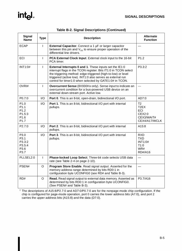
SIGNAL DESCRIPTIONS
ECAP I External Capacitor . Connect a 1 µF or larger capacitor between this pin and VSS to ensure proper operation of the differential line drivers.
—
ECI I PCA External Clock Input . External clock input to the 16-bit PCA timer.
P1.2
INT1:0# I External Interrupts 0 and 1 . These inputs set the IE1:0 interrupt flags in the TCON register. Bits IT1:0 in TCON select the triggering method: edge-triggered (high-to-low) or level triggered (active low). INT1:0 also serves as external run control for timer1:0 when selected by GATE1:0# in TCON.
P3.3:2
OVRI# I Overcurrent Sense (8X930Hx only). Sense input to indicate an overcurrent condition for a bus-powered USB device on an external down-stream port. Active low.
—
P0.7:0 I/O Port 0 . This is an 8-bit, open-drain, bidirectional I/O port. AD7:0
P1.0P1.1P1.2P1.5:3P1.6P1.7
I/O Port 1 . This is an 8-bit, bidirectional I/O port with internal pullups.
T2T2EXECICEX2:0CEX3/WAIT#CEX4/A17/WCLK
P2.7:0 I/O Port 2 . This is an 8-bit, bidirectional I/O port with internal pullups.
A15:8
P3.0P3.1P3.3:2P3.5:4P3.6P3.7
I/O Port 3 . This is an 8-bit, bidirectional I/O port with internal pullups.
RXDTXDINT1:0#T1:0WR#RD#/A16
PLLSEL2:0 I Phase-locked Loop Select . Three-bit code selects USB data rate (see Table 2-4 on page 2-10).
—
PSEN# O Program Store Enable . Read signal output. Asserted for the memory address range determined by bits RD0:1 in configuration byte UCONFIG0 (see RD# and Table B-3).
—
RD# O Read. Read signal output to external data memory. Asserted as determined by bits RD0:1 in configuration byte UCONFIG0. (See PSEN# and Table B-3).
P3.7/A16
Table B-2. Signal Descriptions (Cont inued)
Signal Name Type Description Alternate
Function
† The descriptions of A15:8/P2.7:0 and AD7:0/P0.7:0 are for the nonpage-mode chip configuration. If the chip is configured for page-mode operation, port 0 carries the lower address bits (A7:0), and port 2 carries the upper address bits (A15:8) and the data (D7:0).
B-5

8x930Ax, 8x930Hx USER’S MANUAL
RST I Reset . Reset input to the chip. Holding this pin high for 64 oscillator periods while the oscillator is running resets the device. The port pins are driven to their reset conditions when a voltage greater than VIH1 is applied, whether or not the oscillator is running. This pin has an internal pulldown resistor which allows the device to be reset by connecting a capacitor between this pin and VCC.
Asserting RST when the chip is in idle mode or powerdown mode returns the chip to normal operation.
—
RXD I/O Receive Serial Data . RXD sends and receives data in serial I/O mode 0 and receives data in serial I/O modes 1, 2, and 3.
P3.0
SOF# O Start of Frame . Start of frame pulse. Active low. Asserted for 8 states (see Table 2-4 on page 2-10) when frame timer is locked to USB frame timing and SOF token or artificial SOF is detected.
—
T1:0 I Timer 1:0 External Clock Input . When timer 1:0 operates as a counter, a falling edge on the T1:0 pin increments the count.
P3.5:4
T2 I/O Timer 2 Clock Input/Output . For the timer 2 capture mode, this signal is the external clock input. For the clock-out mode, it is the timer 2 clock output.
P1.0
T2EX I Timer 2 External Input . In timer 2 capture mode, a falling edge initiates a capture of the timer 2 registers. In auto-reload mode, a falling edge causes the timer 2 registers to be reloaded. In the up-down counter mode, this signal determines the count direction: 1 = up, 0 = down.
P1.1
TXD O Transmit Serial Data . TXD outputs the shift clock in serial I/O mode 0 and transmits serial data in serial I/O modes 1, 2, and 3.
P3.1
UPWEN# O USB Power Enable (8X930Hx only). A low signal on this pin applies power to all three external downstream ports.
—
VCC PWR Supply Voltage . Connect this pin to the +5V supply voltage. —
VCCP PWR Supply Voltage for I/O buffers . Connect this pin to the +5V supply voltage.
—
VSS GND Circuit Ground . Connect this pin to ground. —
VSSP GND Circuit Ground for I/O buffers . Connect this pin to ground. —
WAIT# I Real-time Wait State Input. The real-time WAIT# input is enabled by writing a logical ‘1’ to the WCON.0 (RTWE) bit at S:A7H. During bus cycles, the external memory system can signal ‘system ready’ to the microcontroller in real time by controlling the WAIT# input signal on the port 1.6 input.
P1.6/CEX3
Table B-2. Signal Descriptions (Cont inued)
Signal Name Type Description Alternate
Function
† The descriptions of A15:8/P2.7:0 and AD7:0/P0.7:0 are for the nonpage-mode chip configuration. If the chip is configured for page-mode operation, port 0 carries the lower address bits (A7:0), and port 2 carries the upper address bits (A15:8) and the data (D7:0).
B-6

SIGNAL DESCRIPTIONS
WCLK O Wait Clock Output. The real-time WCLK output is driven at port 1.7 (WCLK) by writing a logical ‘1’ to the WCON.1 (RTWCE) bit at S:A7H. When enabled, the WCLK output produces a square wave signal with a period of one-half the oscillator frequency.
P1.7/CEX4/A17
WR# O Write. Write signal output to external memory (Table B-3) P3.6
XTAL1 I Oscillator Amplifier Input . When implementing the on-chip oscillator, connect the external crystal/resonator across XTAL1 and XTAL2. If an external clock source is used, connect it to this pin.
—
XTAL2 O Oscillator Amplifier Output . When implementing the on-chip oscillator, connect the external crystal/resonator across XTAL1 and XTAL2. If an external oscillator is used, leave XTAL2 unconnected.
—
Table B-3. Memory Signal Selections (RD1:0)
RD1:0 A17/P1.7/CEX4/WCLK A16/P3.7/RD# PSEN# P3.6/WR# Features
0 0 A17 A16 Asserted for all addresses
Asserted for writes to all memory locations
256-Kbyte external memory
0 1 P1.7/CEX4/ WCLK
A16 Asserted for all addresses
Asserted for writes to all memory locations
128-Kbyte external memory
1 0 P1.7/CEX4/ WCLK
P3.7 only Asserted for all addresses
Asserted for writes to all memory locations
64-Kbyte external memory. One additional port pin.
1 1 P1.7/CEX4/ WCLK
RD# asserted for addresses≤ 7F:FFFFH
Asserted for addresses≥ 80:0000H
Asserted only for writes to MCS® 51 microcontroller data memory locations.
64-Kbyte external memory. Compatible with MCS 51 microcontrollers.
NOTE: RD1:0 are bits 3:2 of configuration byte UCONFIG0 (Figure 4-3 on page 4-5).
Table B-2. Signal Descriptions (Cont inued)
Signal Name Type Description Alternate
Function
† The descriptions of A15:8/P2.7:0 and AD7:0/P0.7:0 are for the nonpage-mode chip configuration. If the chip is configured for page-mode operation, port 0 carries the lower address bits (A7:0), and port 2 carries the upper address bits (A15:8) and the data (D7:0).
B-7


CRegisters


).
isters
ou-
e C-8
APPENDIX CREGISTERS
This appendix contains reference information for the 8x930 special function registers (SFRsThe SFR map in Table C-1 provides the address and reset value for 8x930Ax SFRs. SFRs withdouble borders are endpoint-indexed. For further information, see “Special Function Reg(SFRs)” on page 3-15.
Table C-2 depicts the 8x930Hx SFRs. SFRs with bold borders are port-indexed. SFRs with dble borders are endpoint-indexed.
Tables C-3 through C-10 list the SFRs by functional category. “SFR Descriptions” on pagcontains descriptive tables of the SFRs arranged alphabetically.
NOTEUse the prefix “S:” with SFR addresses to distinguish them from other addresses.
“Configuration Bytes” on page C-78 shows the two configuration bytes, UCONFIG0 andUCONFIG1. For information on device configuration, see Chapter 4.
C-1
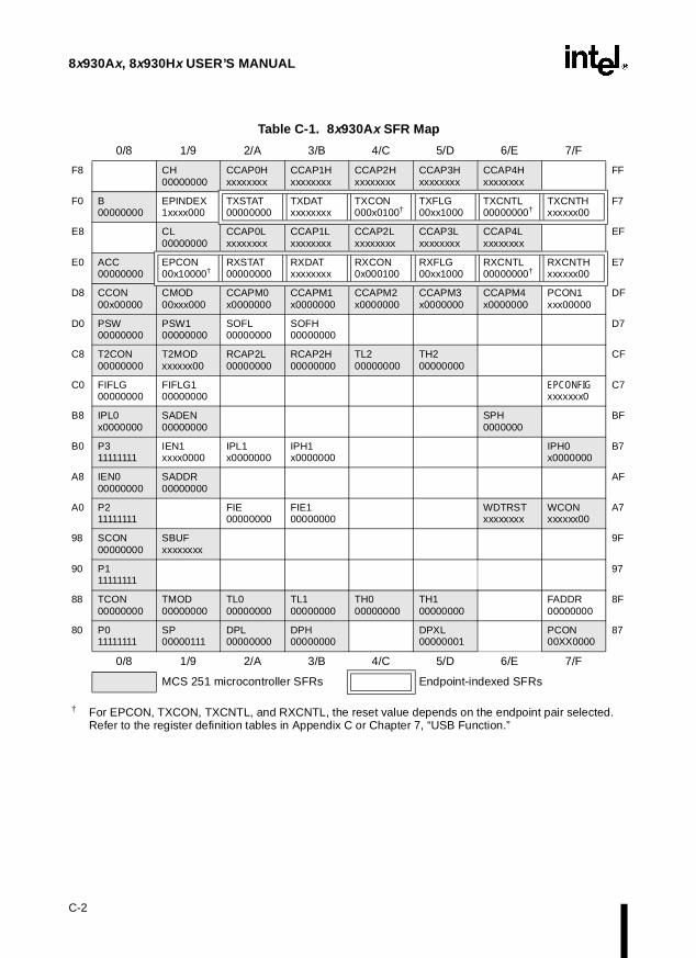
8x930Ax, 8x930Hx USER’S MANUAL
Table C-1. 8x930Ax SFR Map
0/8 1/9 2/A 3/B 4/C 5/D 6/E 7/F
F8 CH 00000000
CCAP0Hxxxxxxxx
CCAP1Hxxxxxxxx
CCAP2Hxxxxxxxx
CCAP3Hxxxxxxxx
CCAP4Hxxxxxxxx
FF
F0 B00000000
EPINDEX1xxxx000
TXSTAT00000000
TXDATxxxxxxxx
TXCON000x0100†
TXFLG00xx1000
TXCNTL00000000†
TXCNTHxxxxxx00
F7
E8 CL00000000
CCAP0Lxxxxxxxx
CCAP1Lxxxxxxxx
CCAP2Lxxxxxxxx
CCAP3Lxxxxxxxx
CCAP4Lxxxxxxxx
EF
E0 ACC00000000
EPCON00x10000†
RXSTAT00000000
RXDATxxxxxxxx
RXCON0x000100
RXFLG00xx1000
RXCNTL00000000†
RXCNTHxxxxxx00
E7
D8 CCON00x00000
CMOD00xxx000
CCAPM0x0000000
CCAPM1x0000000
CCAPM2x0000000
CCAPM3x0000000
CCAPM4x0000000
PCON1xxx00000
DF
D0 PSW00000000
PSW100000000
SOFL00000000
SOFH00000000
D7
C8 T2CON00000000
T2MODxxxxxx00
RCAP2L00000000
RCAP2H00000000
TL200000000
TH200000000
CF
C0 FIFLG00000000
FIFLG100000000
EPCONFIGxxxxxxx0
C7
B8 IPL0x0000000
SADEN00000000
SPH0000000
BF
B0 P311111111
IEN1xxxx0000
IPL1x0000000
IPH1x0000000
IPH0x0000000
B7
A8 IEN000000000
SADDR00000000
AF
A0 P211111111
FIE00000000
FIE100000000
WDTRSTxxxxxxxx
WCONxxxxxx00
A7
98 SCON00000000
SBUFxxxxxxxx
9F
90 P111111111
97
88 TCON00000000
TMOD00000000
TL000000000
TL100000000
TH000000000
TH100000000
FADDR00000000
8F
80 P011111111
SP00000111
DPL00000000
DPH00000000
DPXL00000001
PCON00XX0000
87
0/8 1/9 2/A 3/B 4/C 5/D 6/E 7/F
MCS 251 microcontroller SFRs Endpoint-indexed SFRs
† For EPCON, TXCON, TXCNTL, and RXCNTL, the reset value depends on the endpoint pair selected. Refer to the register definition tables in Appendix C or Chapter 7, “USB Function.”
C-2
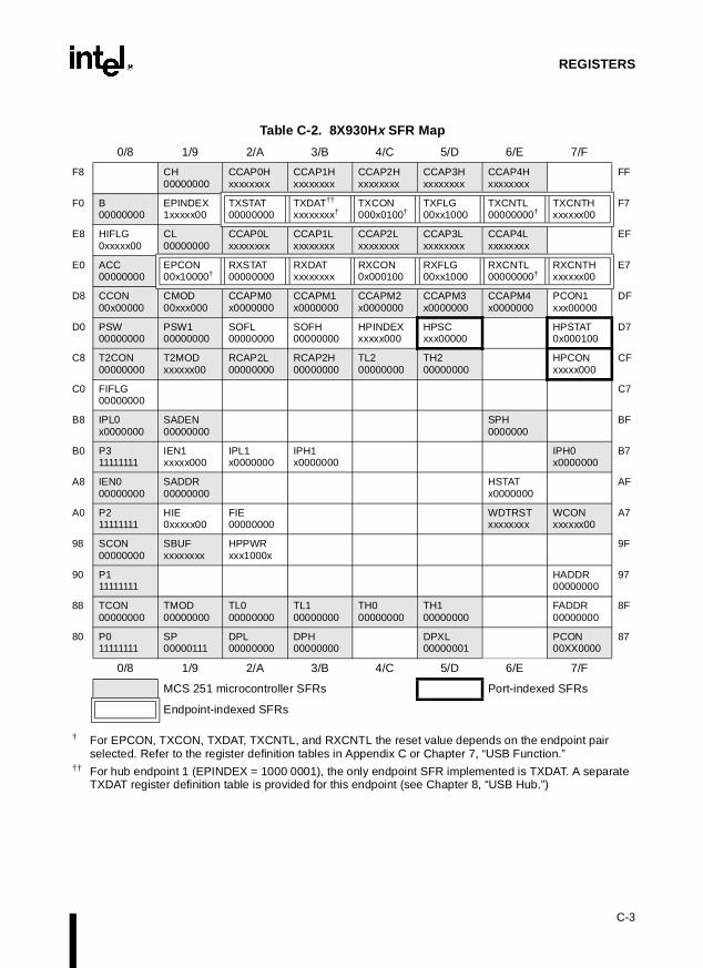
REGISTERS
Table C-2. 8X930Hx SFR Map
0/8 1/9 2/A 3/B 4/C 5/D 6/E 7/F
F8 CH 00000000
CCAP0Hxxxxxxxx
CCAP1Hxxxxxxxx
CCAP2Hxxxxxxxx
CCAP3Hxxxxxxxx
CCAP4Hxxxxxxxx
FF
F0 B00000000
EPINDEX1xxxxx00
TXSTAT00000000
TXDAT††
xxxxxxxx†TXCON000x0100†
TXFLG00xx1000
TXCNTL00000000†
TXCNTHxxxxxx00
F7
E8 HIFLG0xxxxx00
CL00000000
CCAP0Lxxxxxxxx
CCAP1Lxxxxxxxx
CCAP2Lxxxxxxxx
CCAP3Lxxxxxxxx
CCAP4Lxxxxxxxx
EF
E0 ACC00000000
EPCON00x10000†
RXSTAT00000000
RXDATxxxxxxxx
RXCON0x000100
RXFLG00xx1000
RXCNTL00000000†
RXCNTHxxxxxx00
E7
D8 CCON00x00000
CMOD00xxx000
CCAPM0x0000000
CCAPM1x0000000
CCAPM2x0000000
CCAPM3x0000000
CCAPM4x0000000
PCON1xxx00000
DF
D0 PSW00000000
PSW100000000
SOFL00000000
SOFH00000000
HPINDEXxxxxx000
HPSCxxx00000
HPSTAT0x000100
D7
C8 T2CON00000000
T2MODxxxxxx00
RCAP2L00000000
RCAP2H00000000
TL200000000
TH200000000
HPCONxxxxx000
CF
C0 FIFLG00000000
C7
B8 IPL0x0000000
SADEN00000000
SPH0000000
BF
B0 P311111111
IEN1xxxxx000
IPL1x0000000
IPH1x0000000
IPH0x0000000
B7
A8 IEN000000000
SADDR00000000
HSTATx0000000
AF
A0 P211111111
HIE0xxxxx00
FIE00000000
WDTRSTxxxxxxxx
WCONxxxxxx00
A7
98 SCON00000000
SBUFxxxxxxxx
HPPWRxxx1000x
9F
90 P111111111
HADDR00000000
97
88 TCON00000000
TMOD00000000
TL000000000
TL100000000
TH000000000
TH100000000
FADDR00000000
8F
80 P011111111
SP00000111
DPL00000000
DPH00000000
DPXL00000001
PCON00XX0000
87
0/8 1/9 2/A 3/B 4/C 5/D 6/E 7/F
MCS 251 microcontroller SFRs Port-indexed SFRs
Endpoint-indexed SFRs
† For EPCON, TXCON, TXDAT, TXCNTL, and RXCNTL the reset value depends on the endpoint pair selected. Refer to the register definition tables in Appendix C or Chapter 7, “USB Function.”
†† For hub endpoint 1 (EPINDEX = 1000 0001), the only endpoint SFR implemented is TXDAT. A separate TXDAT register definition table is provided for this endpoint (see Chapter 8, “USB Hub.”)
C-3

8x930Ax, 8x930Hx USER’S MANUAL
C.1 SFRS BY FUNCTIONAL CATEGORY
Table C-3. Core SFRs
Mnemonic Name Address
ACC† Accumulator S:E0H
B† B register S:F0H
PSW Program Status Word S:D0H
PSW1 Program Status Word 1 S:D1H
SP† Stack Pointer – LSB of SPX S:81H
SPH† Stack Pointer High – MSB of SPX S:BEH
DPTR† Data Pointer (2 bytes) —
DPL† Low Byte of DPTR S:82H
DPH† High Byte of DPTR S:83H
DPXL† Data Pointer Extended, Low S:85H
PCON Power Control S:87H
PCON1 USB Power Control. S:DFH
WCON Wait State Control Register S:A7H†These SFRs can also be accessed by their corresponding registers in the register file.
Table C-4. Interrupt System SFRs
Mnemonic Description Address
FIE USB Function Interrupt Enable Register. S:A2H
FIE1 USB Function Interrupt Enable Register. S:A3H
FIFLG USB Function Interrupt Flag Register. S:C0H
FIFLG1 USB Function Interrupt Flag Register. S:C1H
HIE Hub Interrupt Enable Register. S:A1H
HIFLG Hub Interrupt Flag Register. S:E8H
IEN0 Interrupt Enable Register 0. S:A8H
IEN1 Interrupt Enable Register1. S:B1H
IPL0 Interrupt Priority Low Register 0. S:B8H
IPH0 Interrupt Priority High Register 0. S:B7H
IPL1 Interrupt Priority Low Register 1. S:B2H
IPH1 Interrupt Priority High Register 1. S:B3H
SOFH Start of Frame High Register. S:D3H
SOFL Start of Frame Low Register. S:D2H
C-4

REGISTERS
Table C-5. I/O Port SFRs
Mnemonic Name Address
P0 Port 0 S:80H
P1 Port 1 S:90H
P2 Port 2 S:A0H
P3 Port 3 S:B0H
Table C-6. Serial I/O SFRs
Mnemonic Name Address
SCON Serial Control S:98H
SBUF Serial Data Buffer S:99H
SADEN Slave Address Mask S:B9H
SADDR Slave Address S:A9H
Table C-7. USB Function SFRs
Mnemonic Name Address
EPCON Endpoint Control Register. S:E1H
EPCONFIG Endpoint Configuration Register S:C7H
EPINDEX Endpoint Index Register. S:F1H
FADDR Function Address Register. S:8FH
RXCNTH Receive FIFO Byte-Count High Register. S:E7H
RXCNTL Receive FIFO Byte-Count Low Register. S:E6H
RXCON Receive FIFO Control Register. S:E4H
RXDAT Receive FIFO Data Register. S:E3H
RXFLG Receive FIFO Flag Register. S:E5H
RXSTAT Endpoint Receive Status Register. S:E2H
TXCNTH Transmit Count High Register. S:F7H
TXCNTL Transmit Count Low Register. S:F6H
TXCON Transmit FIFO Control Register. S:F4H
TXDAT Transmit FIFO Data Register. S:F3H
TXFLG Transmit Flag Register. S:F5H
TXSTAT Endpoint Transmit Status Register. S:FAH
C-5

8x930Ax, 8x930Hx USER’S MANUAL
Table C-8. USB Hub SFRs
Mnemonic Name Address
HADDR Hub Address Register. S:97H
HPCON Hub Port Control. S:CFH
HPINDEX Hub Port Index Register. S:D4H
HPPWR Hub Port Power Control. S:9AH
HPSC Hub Port Status Change. S:D5H
HPSTAT Hub Port Status. S:D7H
HSTAT Hub Status and Configuration. S:AEH
Table C-9. Timer/Counter and Watchdog Timer SFRs
Mnemonic Name Address
TL0 Timer/Counter 0 Low Byte S:8AH
TH0 Timer/Counter 0 High Byte S:8CH
TL1 Timer/Counter 1 Low Byte S:8BH
TH1 Timer/Counter 1 High Byte S:8DH
TL2 Timer/Counter 2 Low Byte S:CCH
TH2 Timer/Counter 2 High Byte S:CDH
TCON Timer/Counter 0 and 1 Control S:88H
TMOD Timer/Counter 0 and 1 Mode Control S:89H
T2CON Timer/Counter 2 Control S:C8H
T2MOD Timer/Counter 2 Mode Control S:C9H
RCAP2L Timer 2 Reload/Capture Low Byte S:CAH
RCAP2H Timer 2 Reload/Capture High Byte S:CBH
WDTRST WatchDog Timer Reset S:A6H
C-6

REGISTERS
Table C-10. Programmable Counter Array (PCA) SFRs
Mnemonic Name Address
CCON PCA Timer/Counter Control S:D8H
CMOD PCA Timer/Counter Mode S:D9H
CCAPM0 PCA Timer/Counter Mode 0 S:DAH
CCAPM1 PCA Timer/Counter Mode 1 S:DBH
CCAPM2 PCA Timer/Counter Mode 2 S:DCH
CCAPM3 PCA Timer/Counter Mode 3 S:DDH
CCAPM4 PCA Timer/Counter Mode 4 S:DEH
CL PCA Timer/Counter Low Byte S:E9H
CH PCA Timer/Counter High Byte S:F9H
CCAP0L PCA Compare/Capture Module 0 Low Byte S:EAH
CCAP1L PCA Compare/Capture Module 1 Low Byte S:EBH
CCAP2L PCA Compare/Capture Module 2 Low Byte S:ECH
CCAP3L PCA Compare/Capture Module 3 Low Byte S:EDH
CCAP4L PCA Compare/Capture Module 4 Low Byte S:EEH
CCAP0H PCA Compare/Capture Module 0 High Byte S:FAH
CCAP1H PCA Compare/Capture Module 1 High Byte S:FBH
CCAP2H PCA Compare/Capture Module 2 High Byte S:FCH
CCAP3H PCA Compare/Capture Module 3 High Byte S:FDH
CCAP4H PCA Compare/Capture Module 4 High Byte S:FEH
C-7
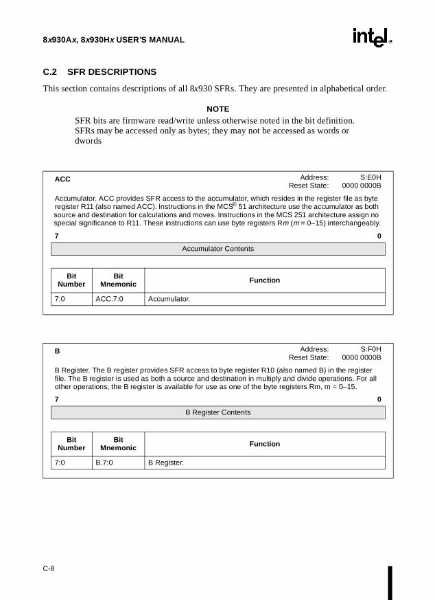
8x930Ax, 8x930Hx USER’S MANUAL
r.
C.2 SFR DESCRIPTIONS
This section contains descriptions of all 8x930 SFRs. They are presented in alphabetical orde
NOTESFR bits are firmware read/write unless otherwise noted in the bit definition. SFRs may be accessed only as bytes; they may not be accessed as words or dwords
ACC Address: S:E0HReset State: 0000 0000B
Accumulator. ACC provides SFR access to the accumulator, which resides in the register file as byte register R11 (also named ACC). Instructions in the MCS® 51 architecture use the accumulator as both source and destination for calculations and moves. Instructions in the MCS 251 architecture assign no special significance to R11. These instructions can use byte registers Rm (m = 0–15) interchangeably.
7 0
Accumulator Contents
Bit Number
Bit Mnemonic Function
7:0 ACC.7:0 Accumulator.
B Address: S:F0HReset State: 0000 0000B
B Register. The B register provides SFR access to byte register R10 (also named B) in the register file. The B register is used as both a source and destination in multiply and divide operations. For all other operations, the B register is available for use as one of the byte registers Rm, m = 0–15.
7 0
B Register Contents
Bit Number
Bit Mnemonic Function
7:0 B.7:0 B Register.
C-8

REGISTERS
CCAPxH, CCAPxL (x = 0–4) Address: CCAP0H,L S:FAH, S:EAHCCAP1H,L S:FBH, S:EBHCCAP2H,L S:FCH, S:ECHCCAP3H,L S:FDH, S:EDHCCAP4H,L S:FEH, S:EEH
Reset State: xxxx xxxxB
PCA Module Compare/Capture Registers. These five register pairs store the 16-bit comparison value or captured value for the corresponding compare/capture modules. In the PWM mode, the low-byte register controls the duty cycle of the output waveform.
7 0
High/Low Byte of Compare/Capture Values
Bit Number
Bit Mnemonic Function
7:0 CCAPxH.7:0
CCAPxL.7:0
High byte of PCA comparison or capture values.
Low byte of PCA comparison or capture values.
C-9

8x930Ax, 8x930Hx USER’S MANUAL
CCAPMx (x = 0–4) Address: CCAPM0 S:DAHCCAPM1 S:DBHCCAPM2 S:DCHCCAPM3 S:DDHCCAPM4 S:DEH
Reset State: x000 0000B
PCA Module Compare/Capture Registers. These five register pairs store the 16-bit comparison value or captured value for the corresponding compare/capture modules. In the PWM mode, the low-byte register controls the duty cycle of the output waveform.
7 0
— ECOMx CAPPx CAPNx MATx TOGx PWMx ECCFx
Bit Number
Bit Mnemonic Function
7 — Reserved:
The value read from this bit is indeterminate. Write a zero to this bit.
6 ECOMx Compare Modes:
ECOMx = 1 enables the module comparator function. The comparator is used to implement the firmware timer, high-speed output, pulse width modulation, and watchdog timer modes.
5 CAPPx Capture Mode (Positive):
CAPPx = 1 enables the capture function with capture triggered by a positive edge on pin CEXx.
4 CAPNx Capture Mode (Negative):
CAPNx = 1 enables the capture function with capture triggered by a negative edge on pin CEXx.
3 MATx Match:
Set ECOMx and MATx to implement the firmware timer mode. When MATx = 1, a match of the PCA timer/counter with the compare/capture register sets the CCFx bit in the CCON register, flagging an interrupt.
2 TOGx Toggle:
Set ECOMx, MATx, and TOGx to implement the high-speed output mode. When TOGx = 1, a match of the PCA timer/counter with the compare/capture register toggles the CEXx pin.
1 PWMx Pulse Width Modulation Mode:
PWMx = 1 configures the module for operation as an 8-bit pulse width modulator with output waveform on the CEXx pin.
0 ECCFx Enable CCFx Interrupt:
Enables compare/capture flag CCFx in the CCON register to generate an interrupt request.
C-10

REGISTERS
CCON Address: S:D8HReset State: 00x0 0000B
PCA Timer/Counter Control Register. Contains the run control bit and overflow flag for the PCA timer/counter, and the compare/capture flags for the five PCA compare/capture modules.
7 0
CF CR — CCF4 CCF3 CCF2 CCF1 CCF0
Bit Number
Bit Mnemonic Function
7 CF PCA Timer/Counter Overflow Flag:
Set by hardware when the PCA timer/counter rolls over. This generates an interrupt request if the ECF interrupt enable bit in CMOD is set. CF can be set by hardware or firmware but can be cleared only by firmware.
6 CR PCA Timer/Counter Run Control Bit:
Set and cleared by firmware to turn the PCA timer/counter on and off.
5 — Reserved:
The value read from this bit is indeterminate. Write a zero to this bit.
4:0 CCF4:0 PCA Module Compare/Capture Flags:
Set by hardware when a match or capture occurs. This generates a PCA interrupt request if the ECCFx interrupt enable bit in the corresponding CCAPMx register is set. Must be cleared by firmware.
CH, CL Address: S:F9HS:E9H
Reset State: 0000 0000B
CH, CL Registers. These registers operate in cascade to form the 16-bit PCA timer/counter.
7 0
High/Low Byte PCA Timer/Counter
Bit Number
Bit Mnemonic Function
7:0 CH.7:0
CL.7:0
High byte of the PCA timer/counter
Low byte of the PCA timer/counter
C-11

8x930Ax, 8x930Hx USER’S MANUAL
CMOD Address: S:D9HReset State: 00xx x000B
PCA Timer/Counter Mode Register. Contains bits for selecting the PCA timer/counter input, disabling the PCA timer/counter during idle mode, enabling the PCA WDT reset output (module 4 only), and enabling the PCA timer/counter overflow interrupt.
7 0
CIDL WDTE — — — CPS1 CPS0 ECF
Bit Number
Bit Mnemonic Function
7 CIDL PCA Timer/Counter Idle Control:
CIDL = 1 disables the PCA timer/counter during idle mode. CIDL = 0 allows the PCA timer/counter to run during idle mode.
6 WDTE Watchdog Timer Enable:
WDTE = 1 enables the watchdog timer output on PCA module 4.WDTE = 0 disables the PCA watchdog timer output.
5:3 — Reserved:
Values read from these bits are indeterminate. Write zeros to these bits.
2:1 CPS1:0 PCA Timer/Counter Input Select:
CPS1 CPS0
0 0 FCLK /60 1 FCLK /21 0 Timer 0 overflow1 1 External clock at ECI pin (maximum rate = FOSC /8 )
0 ECF PCA Timer/Counter Interrupt Enable:
ECF = 1 enables the CF bit in the CCON register to generate an interrupt request.
C-12

REGISTERS
DPH Address: S:83HReset State: 0000 0000B
Data Pointer High. DPH provides SFR access to register file location 58 (also named DPH). DPH is the upper byte of the 16-bit data pointer, DPTR. Instructions in the MCS® 51 architecture use DPTR for data moves, code moves, and for a jump instruction (JMP @A+DPTR). See also DPL and DPXL.
7 0
DPH Contents
Bit Number
Bit Mnemonic Function
7:0 DPH.7:0 Data Pointer High:
Bits 8–15 of the extended data pointer, DPX (DR56).
DPL Address: S:82HReset State: 0000 0000B
Data Pointer Low. DPL provides SFR access to register file location 59 (also named DPL). DPL is the low byte of the 16-bit data pointer, DPTR. Instructions in the MCS® 51 architecture use the 16-bit data pointer for data moves, code moves, and for a jump instruction (JMP @A+DPTR). See also DPH and DPXL.
7 0
DPL Contents
Bit Number
Bit Mnemonic Function
7:0 DPL.7:0 Data Pointer Low:
Bits 0–7 of the extended data pointer, DPX (DR56).
C-13

8x930Ax, 8x930Hx USER’S MANUAL
DPXL Address: S:85HReset State: 0000 0001B
Data Pointer Extended Low. DPXL provides SFR access to register file location 57 (also named DPXL). Location 57 is the lower byte of the upper word of the extended data pointer, DPX = DR56, whose lower word is the 16-bit data pointer, DPTR. See also DPH and DPL.
7 0
DPXL Contents
Bit Number
Bit Mnemonic Function
7:0 DPXL.7:0 Data Pointer Extended Low:
Bits 16–23 of the extended data pointer, DPX (DR56).
C-14
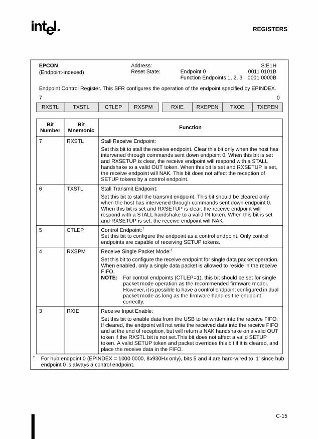
REGISTERS
EPCON(Endpoint-indexed)
Address: S:E1HReset State: Endpoint 0 0011 0101B
Function Endpoints 1, 2, 3 0001 0000B
Endpoint Control Register. This SFR configures the operation of the endpoint specified by EPINDEX.
7 0
RXSTL TXSTL CTLEP RXSPM RXIE RXEPEN TXOE TXEPEN
Bit Number
Bit Mnemonic Function
7 RXSTL Stall Receive Endpoint:
Set this bit to stall the receive endpoint. Clear this bit only when the host has intervened through commands sent down endpoint 0. When this bit is set and RXSETUP is clear, the receive endpoint will respond with a STALL handshake to a valid OUT token. When this bit is set and RXSETUP is set, the receive endpoint will NAK. This bit does not affect the reception of SETUP tokens by a control endpoint.
6 TXSTL Stall Transmit Endpoint:
Set this bit to stall the transmit endpoint. This bit should be cleared only when the host has intervened through commands sent down endpoint 0. When this bit is set and RXSETUP is clear, the receive endpoint will respond with a STALL handshake to a valid IN token. When this bit is set and RXSETUP is set, the receive endpoint will NAK
5 CTLEP Control Endpoint:†
Set this bit to configure the endpoint as a control endpoint. Only control endpoints are capable of receiving SETUP tokens.
4 RXSPM Receive Single Packet Mode:†
Set this bit to configure the receive endpoint for single data packet operation. When enabled, only a single data packet is allowed to reside in the receive FIFO. NOTE: For control endpoints (CTLEP=1), this bit should be set for single
packet mode operation as the recommended firmware model. However, it is possible to have a control endpoint configured in dual packet mode as long as the firmware handles the endpoint correctly.
3 RXIE Receive Input Enable:
Set this bit to enable data from the USB to be written into the receive FIFO. If cleared, the endpoint will not write the received data into the receive FIFO and at the end of reception, but will return a NAK handshake on a valid OUT token if the RXSTL bit is not set.This bit does not affect a valid SETUP token. A valid SETUP token and packet overrides this bit if it is cleared, and place the receive data in the FIFO.
† For hub endpoint 0 (EPINDEX = 1000 0000, 8x930Hx only), bits 5 and 4 are hard-wired to ‘1’ since hub endpoint 0 is always a control endpoint.
C-15

8x930Ax, 8x930Hx USER’S MANUAL
2 RXEPEN Receive Endpoint Enable:
Set this bit to enable the receive endpoint. When disabled, the endpoint does not respond to a valid OUT or SETUP token. This bit is hardware read-only and has the highest priority among RXIE and RXSTL. Note that endpoint 0 is enabled for reception upon reset.
1 TXOE Transmit Output Enable:
This bit is used to enable the data in TXDAT to be transmitted. If cleared, the endpoint returns a NAK handshake to a valid IN token if the TXSTL bit is not set.
0 TXEPEN Transmit Endpoint Enable:
This bit is used to enable the transmit endpoint. When disabled, the endpoint does not respond to a valid IN token. This bit is hardware read only. Note that endpoint 0 is enabled for transmission upon reset.
EPCON (Continued)(Endpoint-indexed)
Address: S:E1HReset State: Endpoint 0 0011 0101B
Function Endpoints 1, 2, 3 0001 0000B
Endpoint Control Register. This SFR configures the operation of the endpoint specified by EPINDEX.
7 0
RXSTL TXSTL CTLEP RXSPM RXIE RXEPEN TXOE TXEPEN
Bit Number
Bit Mnemonic Function
† For hub endpoint 0 (EPINDEX = 1000 0000, 8x930Hx only), bits 5 and 4 are hard-wired to ‘1’ since hub endpoint 0 is always a control endpoint.
C-16

REGISTERS
EPCONFIG† Address: S:C7HReset State: xxxx xxx0B
Endpoint Configuration Register. Selects the six-endpoint pair option or four-endpoint pair option as the 8x930Ax function endpoint pair configuration.
7 0
— — — — — — — SIXEPPEN
Bit Number
Bit Mnemonic Function
7:1 — Reserved:
Write zeroes to these bits.
0 SIXEPPEN Six-endpoint pair enable:††
Set this bit to select the six-endpoint pair (6EPP) configuration, which provides the following FIFO sizes (bytes).
EPINDEX FFSZ1:0
0xxx x000 xx0xxx x001 00†††
0xxx x010 xx0xxx x011 xx0xxx x100 xx0xxx x101 xx
TransmitFIFO
1625632323216
ReceiveFIFO
1625632323216
Clear this bit to select the four-endpoint pair (4EPP) configuration, which provides the following FIFO sizes (bytes).
EPINDEX FFSZ1:0
0xxx xx00 xx0xxx xx01 00
011011
0xxx xx10 xx0xxx xx11 xx
TransmitFIFO
162565121024
01616
ReceiveFIFO
162565120
10241616
† 8x930Ax only. Early sample devices did not have this SFR.†† Select the endpoint configuration during initialization and do not change during program execution.††† When using function endpoint 1 in the six-endpoint pair configuration, clear the FFSZ1:0 bits in
TXCON to select the 256-byte size for the transmit and receive FIFOs.
C-17

8x930Ax, 8x930Hx USER’S MANUAL
EPINDEX Address: S:F1HReset State: 1xxx x000B
Endpoint Index Register. This register identifies the endpoint pair. Its contents select the transmit and receive FIFO pair and serve as an index to endpoint-specific SFRs.
7 0
8X930Hx HORF — — — — — EPINX1 EPINX0
7 0
8X930Ax4 EPP
— — — — — — EPINX1 EPINX0
7 0
8X930Ax 6 EPP
— — — — — EPINX2 EPINX1 EPINX0
BitNumber
BitMnemonic Function
7 HORF
(8X930Hx)
Hub/function Bit:
1 = Hub. Selects USB hub FIFOs and SFRs.0 = Function. Selects USB function FIFOs and SFRs.
—(8X930Ax)
Reserved:
Although the reset state for this bit is “1”, always write a zero to this bit for 8X930Ax applications.
6:3 — Reserved:
Write zeros to these bits.
2 —
8X930Hx or8X930Ax(4 EPP)
Reserved:
Write a zero to this bit. 8x930Hx
1:0 EPINX1:0
8X930Hxor
8X930Ax(4 EPP)
Endpoint Index:
EPINDEX†
0xxx xx00 Function Endpoint 00xxx xx01 Function Endpoint 10xxx xx10 Function Endpoint 20xxx xx11 Function Endpoint 3
EPINDEX† (8x930Hx only)1xxx xx00 Hub Endpoint 01xxx xx01 Hub Endpoint 1
2:0 EPINX2:0
8X930Ax (6 EPP)
Endpoint Index:
EPINDEX†
0xxx x000 Function Endpoint 00xxx x001 Function Endpoint 10xxx x010 Function Endpoint 20xxx x011 Function Endpoint 30xxx x100 Function Endpoint 40xxx x101 Function Endpoint 5
† The EPINDEX register identifies the endpoint pair and selects the associated transmit and receive FIFO pair. The value in this register plus SFR addresses select the associated bank of endpoint-indexed SFRs (TXDAT, TXCON, TXFLG, TXCNTH/L, RXDAT, RXCON, RXFLG, RXCNTH/L, EPCON, TXSTAT, and RXSTAT).
C-18

REGISTERS
FADDR Address: S:8FHReset State: 0000 0000B
Function Address Register. This SFR holds the address for the USB function. During bus enumeration it is written with a unique value assigned by the host.
7 0
— A6:0
Bit Number
Bit Mnemonic Function
7 — Reserved:
Write a zero to this bit.
6:0 A6:0 7-bit Programmable Function Address:
This register is programmed through the commands received via endpoint 0 on configuration, which should be the only time the firmware should change the value of this register. This register is read-only by hardware.
C-19

8x930Ax, 8x930Hx USER’S MANUAL
FIE Address: S:A2HReset State: 0000 0000B
Function Interrupt Enable Register. Enables and disables the receive and transmit done interrupts for the four function endpoints.
7 0
FRXIE3 FTXIE3 FRXIE2 FTXIE2 FRXIE1 FTXIE1 FRXIE0 FTXIE0
Bit Number
Bit Mnemonic Function
7 FRXIE3 Function Receive Interrupt Enable 3:
Enables receive done interrupt for endpoint 3 (FRXD3).
6 FTXIE3 Function Transmit Interrupt Enable 3:
Enables transmit done interrupt for endpoint 3 (FTXD3).
5 FRXIE2 Function Receive Interrupt Enable 2:
Enables the receive done interrupt for endpoint 2 (FRXD2).
4 FTXIE2 Function Transmit Interrupt Enable 2:
Enables the transmit done interrupt for endpoint 2 (FTXD2).
3 FRXIE1 Function Receive Interrupt Enable 1:
Enables the receive done interrupt for endpoint 1 (FRXD1).
2 FTXIE1 Function Transmit Interrupt Enable 1:
Enables the transmit done interrupt for endpoint 1 (FTXD1).
1 FRXIE0 Function Receive Interrupt Enable 0:
Enables the receive done interrupt for endpoint 0 (FRXD0).
0 FTXIE0 Function Transmit Interrupt Enable 0:
Enables the transmit done interrupt for endpoint 0 (FTXD0).
NOTE: For all bits, a ‘1’ means the interrupt is enabled and will cause an interrupt to be signaled to the microcontroller. A ‘0’ means the associated interrupt source is disabled and cannot cause an interrupt, even though the interrupt bit’s value is still reflected in the FIFLG register.
C-20
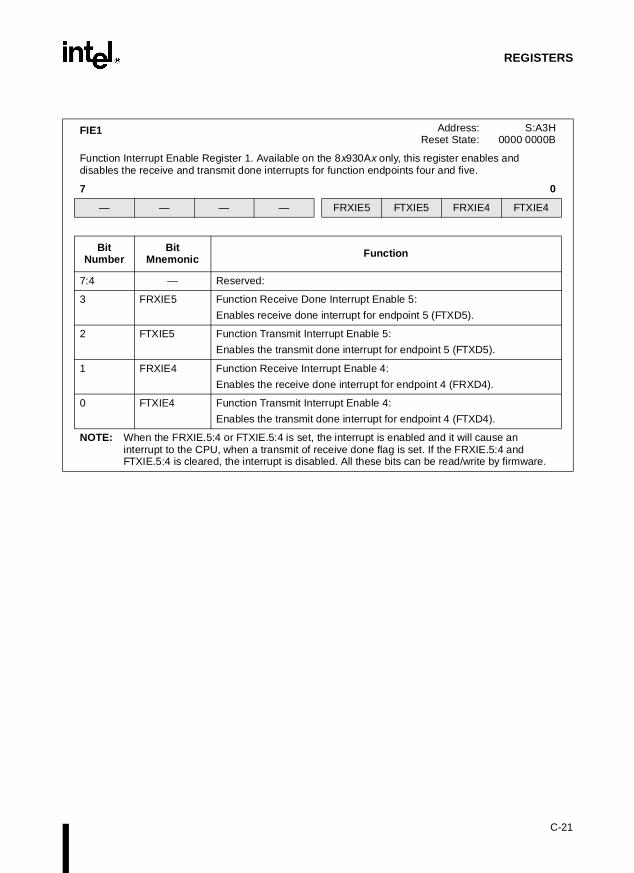
REGISTERS
FIE1 Address: S:A3HReset State: 0000 0000B
Function Interrupt Enable Register 1. Available on the 8x930Ax only, this register enables and disables the receive and transmit done interrupts for function endpoints four and five.
7 0
— — — — FRXIE5 FTXIE5 FRXIE4 FTXIE4
Bit Number
Bit Mnemonic Function
7:4 — Reserved:
3 FRXIE5 Function Receive Done Interrupt Enable 5:
Enables receive done interrupt for endpoint 5 (FTXD5).
2 FTXIE5 Function Transmit Interrupt Enable 5:
Enables the transmit done interrupt for endpoint 5 (FTXD5).
1 FRXIE4 Function Receive Interrupt Enable 4:
Enables the receive done interrupt for endpoint 4 (FRXD4).
0 FTXIE4 Function Transmit Interrupt Enable 4:
Enables the transmit done interrupt for endpoint 4 (FTXD4).
NOTE: When the FRXIE.5:4 or FTXIE.5:4 is set, the interrupt is enabled and it will cause an interrupt to the CPU, when a transmit of receive done flag is set. If the FRXIE.5:4 and FTXIE.5:4 is cleared, the interrupt is disabled. All these bits can be read/write by firmware.
C-21

8x930Ax, 8x930Hx USER’S MANUAL
FIFLG Address: S:C0HReset State: 0000 0000B
Function Interrupt Flag Register. Contains the USB Function’s Transmit and Receive Done interrupt flags for non-isochronous endpoints.
7 0
FRXD3 FTXD3 FRXD2 FTXD2 FRXD1 FTXD1 FRXD0 FTXD0
Bit Number
Bit Mnemonic Function
7 FRXD3 Function Receive Done Flag, Endpoint 3
6 FTXD3 Function Transmit Done Flag, Endpoint 3
5 FRXD2 Function Receive Done Flag, Endpoint 2
4 FTXD2 Function Transmit Done Flag, Endpoint 2
3 FRXD1 Function Receive Done Flag, Endpoint 1
2 FTXD1 Function Transmit Done Flag, Endpoint 1
1 FRXD0 Function Receive Done Flag, Endpoint 0
0 FTXD0 Function Transmit Done Flag, Endpoint 0
NOTES:1. For all bits in the Interrupt Flag Register, a ‘1’ indicates that an interrupt is actively pending; a ‘0’
indicates that the interrupt is not active. The interrupt status is shown regardless of the state of the corresponding interrupt enable bit in the FIE.
2. Bits are set-only by hardware and clearable in firmware. Firmware can also set the bits for test purposes, allowing the interrupt to be generated in firmware.
3. A set bit indicates either: Valid data waiting to be serviced in the RX FIFO for the indicated endpoint and that the data was received without error and has been acknowledged; or Data was received with a Receive Data Error requiring firmware intervention to be cleared.
C-22

REGISTERS
FIFLG1 Address: S:C1HReset State: 0000 0000B
Function Interrupt Flag Register 1. Available on the 8x930Ax only, this register contains the USB Function’s Transmit and Receive Done interrupt flags for non-isochronous endpoints.
7 0
— — — — FRXD5 FTXD5 FRXD4 FTXD4
Bit Number
Bit Mnemonic Function
7:4 — Reserved:
Write zeros to these bits.
3 FTXD5 Function Receive Done Flag, Endpoint 5:
2 FTXD5 Function Transmit Done Flag, Endpoint 5:
1 FRXD4 Function Receive Done Flag, Endpoint 4:
0 FTXD4 Function Transmit Done Flag, Endpoint 4:
NOTES:1. For all bits in the Interrupt Flag Register, a ‘1’ indicates that an interrupt is actively pending; a ‘0’
indicates that the interrupt is not active. The interrupt status is shown regardless of the state of the corresponding interrupt enable bit in the FIE.
2. Bits are set-only by hardware and clearable in firmware. Firmware can also set the bits for test purposes, allowing the interrupt to be generated in firmware.
3. A set bit indicates either: Valid data waiting to be serviced in the RX FIFO for the indicated endpoint and that the data was received without error and has been acknowledged; or Data was received with a Receive Data Error requiring firmware intervention to be cleared.
C-23

8x930Ax, 8x930Hx USER’S MANUAL
HADDR Address: S:97HReset State: 0000 0000B
Hub Address Register. This SFR holds the address for the hub device. During bus enumeration it is written with a unique value assigned by the host.
7 0
— Hub Address
Bit Number Function
7 Reserved.
Write a zero to this bit.
6:0 Hub address register:
Updated using a SET_ADDRESS USB host request. This address is used by the HIU to perform token decoding.
HIE Address: S:A1HReset State: 0xxx xx00B
Hub Interrupt Enable Register. Enables and disables the receive and transmit done interrupts for hub endpoint 0.
7 0
— — — — — HRXE0 HTXE0
Bit Number
Bit Mnemonic Function
7:2 — Reserved:
Write zeros to these bits.
1 HRXE0 HRXE0:
Enable the hub endpoint 0 receive done interrupt (HRXD0).†
0 HTXE0 HTXE0:
Enable the hub endpoint 0 transmit done interrupt (HTXD0).†
† For both bits, a ‘1’ means the interrupt is enabled, and will cause an interrupt to be signaled to the microcontroller. A ‘0’ means the associated interrupt source is disabled and cannot cause an interrupt, even though its value is still reflected in the HIFLG register.
C-24
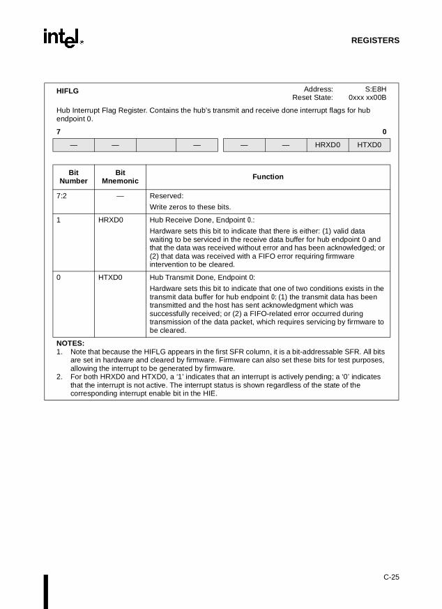
REGISTERS
HIFLG Address: S:E8HReset State: 0xxx xx00B
Hub Interrupt Flag Register. Contains the hub’s transmit and receive done interrupt flags for hub endpoint 0.
7 0
— — — — — HRXD0 HTXD0
Bit Number
Bit Mnemonic Function
7:2 — Reserved:
Write zeros to these bits.
1 HRXD0 Hub Receive Done, Endpoint 0.:
Hardware sets this bit to indicate that there is either: (1) valid data waiting to be serviced in the receive data buffer for hub endpoint 0 and that the data was received without error and has been acknowledged; or (2) that data was received with a FIFO error requiring firmware intervention to be cleared.
0 HTXD0 Hub Transmit Done, Endpoint 0:
Hardware sets this bit to indicate that one of two conditions exists in the transmit data buffer for hub endpoint 0: (1) the transmit data has been transmitted and the host has sent acknowledgment which was successfully received; or (2) a FIFO-related error occurred during transmission of the data packet, which requires servicing by firmware to be cleared.
NOTES:1. Note that because the HIFLG appears in the first SFR column, it is a bit-addressable SFR. All bits
are set in hardware and cleared by firmware. Firmware can also set these bits for test purposes, allowing the interrupt to be generated by firmware.
2. For both HRXD0 and HTXD0, a ‘1’ indicates that an interrupt is actively pending; a ‘0’ indicates that the interrupt is not active. The interrupt status is shown regardless of the state of the corresponding interrupt enable bit in the HIE.
C-25

8x930Ax, 8x930Hx USER’S MANUAL
HPCON Address: S:CFH Reset State: xxxx x000B
Hub Port Control Register. Firmware writes to this register to disable, enable, reset, suspend, and resume a port.
7 0
— — — — — HPCON2 HPCON1 HPCON0
Bit Number
Bit Mnemonic Function
7:3 — Reserved:
Write zeros to these bits.
2:0 HPCON.2:0 Encoded Hub Port Control Commands:
All bits should be set and cleared by firmware after receiving the USB requests ClearPortFeature and SetPortFeature from the host. The bits are encoded as follows (all other bit combinations are ignored by the hardware):
000 — Disable port001 — Enable port010 — Reset and enable port011 — Suspend port100 — Resume port
See Table 8-6 for a complete description of the encoded hub port control commands.
C-26

REGISTERS
HPINDEX Address S:D4HReset State xxxx x000B
Hub Port Index Register. This register contains the binary value of the port whose HPSC, HPSTAT, and HPCON registers are to be accessed.
7 0
— — — — — HPIDX2 HPIDX1 HPIDX0
Bit Number
Bit Mnemonic Function
7:3 — Reserved:
Write zeros to these bits.
2:0 HPIDX.2:0 Port Index Select:
Used to select the port to be indexed by the following registers: HPSC, HPSTAT, and HPCON. This register is hardware read-only. The ports are addressed using the following HPID.2:0 bit combinations:
Port 1 = “001”Port 2 = “010”Port 3 = “011”Port 4 = “100” (internal port)
NOTE: Port 0 = “000” (the root port) and all other combinations not shown above are not valid port indexes and are ignored.
C-27

8x930Ax, 8x930Hx USER’S MANUAL
HPPWR Address: S:9AHReset State: xxx1 000xB
Hub Port Power Control Register. This register is used to control power to the hub’s downstream ports.
7 0
— — — HPPWR.4 HPPWR.3 HPPWR.2 HPPWR.1 —
Bit Number
Bit Mnemonic Function
7:5 — Reserved:
The value read from these bits is indeterminate. Write zeros to these bits.
4 HPPWR.4 Port Power Control Register for USB Port 4 (read-only):
Port 4 is an internal port and is always powered on. This bit is hard-wired to ‘1.’
3:1 HPPWR.3.1 Port Power Control Register for USB Ports 1-3:
Bit 3 is power control for port 3, bit 2 for port 2, and bit 1 for port 1. These bits are set and cleared by firmware via a USB host request SetPortFeature with the PORT_POWER feature selector. These bits will also be cleared by hardware upon detection of an over-current condition. This is done to prevent oscillation of the UPWEN# pin during an over-current condition with bus-powered devices.
A value of ‘1’ enables power to the downstream port and puts the port in a disconnected state. A value of ‘0’ turns the downstream port power off. NOTE: The UPWEN# pin is set to ‘1’ only if all three port power enable
bits (bits 3:1) are ‘0,’ due to the use of a ganged (shared) power enable scheme.
0 — Reserved:
The value read from this bit is indeterminate. Write a zero to this bit.
C-28

REGISTERS
HPSC Address: S:D5HReset State: xxx0 0000B
Hub Port Status Change Register. This register indicates a change in status for a port, including over-current, reset, suspend, enable and connect status.
7 0
— — — RSTSC — PSSC PESC PCSC
Bit Number
Bit Mnemonic Function
7:5 — Reserved:
Write zeros to these bits.
4 RSTSC Reset Status Change (read-, clear-only):
This bit is cleared in firmware via the USB host request ClearPortFeature with a C_PORT_RESET feature selector. ‘1’ indicates reset of port complete; ‘0’ indicates no change.
Port x (x=1,2,3): This bit is set by hardware approximately 10 msec after receipt of a port reset and enable command (SetPortFeature with PORT_RESET feature selector).
Port 4: This bit is set by hardware at the EOF2 point near the end of a frame after completion of the hardware-timed reset due to firmware execution of a port reset and enable command (SetPortFeature with PORT_RESET feature selector).
3 — Reserved:
Write a zero to this bit.
2 PSSC Port Suspend Status Change (read-, clear-only):
This bit is cleared by firmware upon a USB host request ClearPortFeature with C_PORT_SUSPEND feature selector. ‘1’ = resume process complete; ‘0’ = no change. The resume process is initiated by firmware upon reception of a SetPortFeature request with a PORT_SUSPEND feature selector.
Port x (x=1,2,3): This bit is set by hardware upon completion of the firmware-initiated resume process.
Port 4: This bit is set by hardware 20 msec after the next EOF2 point after completion of the resume process.
NOTE: Bits are returned as part of the second word (2 bytes) in response to a Get Port Status request from the USB host. The upper 11 MSbs are reserved and always ‘0’ per USB 1.0: 0000 0000 000.4.3.2.1.0 (MSB at left)
C-29

8x930Ax, 8x930Hx USER’S MANUAL
1 PESC Port Enable/Disable Status Change (read, clear-only):
This bit’s status does not change due to USB requests. This bit is cleared by firmware via the USB host request ClearPortFeature with a C_PORT_ENABLE feature selector. ‘1’ indicates port enabled/ disabled status change; ‘0’ indicates no change.
Port x (x=1,2,3): This bit is set by hardware due to hardware events only (this bit indicates the port was disabled due to babble, physical disconnects, or overcurrent).
Port 4: This bit is set by hardware at the EOF2 point near the end of frame due to hardware events only (e.g., the port was disabled due to babble).
0 PCSC Port Connect Status Change (read-, clear-only):
This bit is cleared by firmware via a USB host request ClearPortFeature with C_PORT_CONNECTION feature selector. ‘1’ indicates connect status change; ‘0’ indicates no change.
Port x (x=1,2,3): This bit is set by hardware at the EOF2 point near the end of a frame due to hardware connects and disconnects.
Port 4: This bit is set by hardware at the next EOF2 after completion of a hub reset (since the internal port is always connected).
HPSC (Continued) Address: S:D5HReset State: xxx0 0000B
Hub Port Status Change Register. This register indicates a change in status for a port, including over-current, reset, suspend, enable and connect status.
7 0
— — — RSTSC — PSSC PESC PCSC
Bit Number
Bit Mnemonic Function
NOTE: Bits are returned as part of the second word (2 bytes) in response to a Get Port Status request from the USB host. The upper 11 MSbs are reserved and always ‘0’ per USB 1.0: 0000 0000 000.4.3.2.1.0 (MSB at left)
C-30

REGISTERS
HPSTAT Address: S:D7HReset State: 0x00 0100B
Hub Port Status Register. This register indicates the current status for a port, including power, reset, suspend, low-speed device, enable, connect, DP, and DM status.
7 0
DPSTAT DMSTAT LSSTAT PPSTAT PRSTAT PSSTAT PESTAT PCSTAT
Bit Number
Bit Mnemonic Function
7 DPSTAT DP Status (read-only):
Value of DP for port x at end of last frame. Firmware must return this bit in response to a GetBusState request from the host.
Port x (x=1,2,3): Set and cleared by hardware at the EOF2 point near the end of a frame (used for diagnostics).
Port 4: Hard-wired to ’1’, since there is no DP signal for the embedded port
6 DMSTAT DM Status (read-only):
Value of DM for port x at end of last frame. Firmware must return this bit in response to a GetBusState request from the host.
Port x (x=1,2,3): Set and cleared by hardware at the EOF2 point near the end of a frame (used for diagnostics).
Port 4: Hard-wired to ’0’, since there is no DM signal for the embedded port.
4 PPSTAT Port Power Status (read-only):
Port x (x=1,2,3): Set and cleared by hardware based on the present power status of the port, as controlled either by firmware using the HPPWR register, or by an overcurrent condition in hardware. ‘1’ = port x is powered on. ‘0’ = port x is powered off. The port x power status is only sampled at the EOF2 point near end-of-frame.
Port 4: Hard-wired to ’1’, since the internal function is always powered-on.
5 LSSTAT Low-speed Device Attach Status (read-only):
Port x (x=1,2,3): Set and cleared by hardware upon detection of the presence or absence of a low-speed device at the EOF2 point near end-of-frame. ‘1’ = low-speed device is attached to port x. ‘0’ = full-speed device is attached to port x.
Port 4: Hard-wired to ’0’ (full-speed), since port 4 is permanently attached to the embedded USB function.
NOTES:
Firmware returns the bits of this register in the first word of the 8x930Hx’ response to the host’s GetPortStatus request. See “GetPortStatus Request Firmware” on page 9-24.
Overcurrent indication is not represented on a per-port basis because the 8x930Hx supports ganged power control and overcurrent indication.
C-31

8x930Ax, 8x930Hx USER’S MANUAL
3 PRSTAT Port Reset Status (read-only):
Port x (x=1,2,3): Set and cleared by hardware as a result of initiating a port x reset by writing to HPCON. ‘1’ = reset signaling is currently asserted for port x. ‘0’ = reset signaling is not asserted. Sampled only at the EOF2 point near end of frame.
Port 4: Same as port x.
2 PSSTAT Port Suspend Status (read-only):
Port x (x=1,2,3): Set and cleared by hardware as controlled by firmware via HPCON. ‘1’ = port x is currently suspended. ‘0’ = not suspended. Sampled only at the EOF2 point near end of frame.
Port 4: Same as port x.
1 PESTAT Port Enable/Disable Status (read-only):
Port x (x=1,2,3): Set and cleared by hardware as controlled by firmware via HPCON. ‘1’ = port x is currently enabled. ‘0’ = port is disabled. Sampled only at the EOF2 point near end of frame.
Port 4: Same as port x.
0 PCSTAT Port Connect Status (read-only):
Port x connect status from previous frame time.
Port x (x=1,2,3): Set and cleared by hardware after sampling the connect state at EOF2 near the end of the present frame. ‘1’ = device is present on port x. ‘0’ = device is not present. This bit will be set if either a physical connection is detected, or during a hub reset when a downstream device is already connected. This bit will be cleared if a disconnect is detected.
Port 4: Hard-wired to ‘1’, since the internal function is permanently connected.
HPSTAT (Continued) Address: S:D7HReset State: 0x00 0100B
Hub Port Status Register. This register indicates the current status for a port, including power, reset, suspend, low-speed device, enable, connect, DP, and DM status.
7 0
DPSTAT DMSTAT LSSTAT PPSTAT PRSTAT PSSTAT PESTAT PCSTAT
Bit Number
Bit Mnemonic Function
NOTES:
Firmware returns the bits of this register in the first word of the 8x930Hx’ response to the host’s GetPortStatus request. See “GetPortStatus Request Firmware” on page 9-24.
Overcurrent indication is not represented on a per-port basis because the 8x930Hx supports ganged power control and overcurrent indication.
C-32

REGISTERS
HSTAT Address: S:AEHReset State: x000 0000B
Hub Status and Configuration Register. This SFR contains bits for remote wake-up request, status and status change indicators for over-current and hub endpoint 1 stall and enable.
7 0
— HRWUPE EP1STL EP1EN OVISC — OVI —
Bit Number
Bit Mnemonic Function
7 — Reserved:
The value read from this bit is indeterminate. Write a zero to this bit.
6 HRWUPE Hub Remote Wake-up Enable Bit:
Set if the device is currently enabled to request remote wake-up. This bit is modified through the SetFeature and ClearFeature requests using the DEVICE_REMOTE_WAKEUP feature selector. When ‘0,’ a hub cannot propagate resume signaling for connect/disconnect and resume events detected on downstream ports.NOTE: Do not set this bit until after the hub is enumerated and the host
issues a SET_FEATURE command with a DEVICE_ REMOTE_WAKEUP feature selector.
5 EP1STL Hub Endpoint 1 Stall Field:
Set to ‘1’ via the USB SetFeature request with endpoint stall feature selector. When ‘1,’ will force a stall response when endpoint 1 is addressed. Reset with USB ClearFeature request with endpoint stall feature selector.
4 EP1EN Hub Endpoint 1 Enable:
Set to ‘1’ upon receipt of a USB SetConfiguration request value of 0001H. Endpoint 1 cannot respond unless this bit is set. Bit is reset upon receipt of configuration value other than 0001H or a system or USB reset.NOTE: This bit must be set in order for the UPWEN# pin to enable
power to the downstream ports. Downstream power cannot be applied until this is done.
3 OVISC Hub Over-current Indicator Status Change (read/clear-only): †
Set to ‘1’ if change is detected in the over-current status, even if the condition goes away before it is detected by firmware. Cleared via a USB ClearFeature request with C_HUB_OVER_CURRENT feature selector. Cleared to ‘0’ if no change.
2 — Reserved:
The value read from this bit is indeterminate. Write a zero to this bit.† Bits 3:0 are returned in response to a Get Hub Status request from the USB host. This response is a
four-byte field with zero padding (MSB at left): 0000 0000 0000 00[3] 0 0000 0000 0000 00[1] 0.
C-33

8x930Ax, 8x930Hx USER’S MANUAL
1 OVI Latest Over-current Indicator (read-only): †
Hardware sets and clears this bit via the OVRI# input pin.‘1’ indicates an over-current condition. ‘0’ indicates normal power operation.
0 — Reserved:
The value read from this bit is indeterminate. Write a zero to this bit.
HSTAT (Continued) Address: S:AEHReset State: x000 0000B
Hub Status and Configuration Register. This SFR contains bits for remote wake-up request, status and status change indicators for over-current and hub endpoint 1 stall and enable.
7 0
— HRWUPE EP1STL EP1EN OVISC — OVI —
Bit Number
Bit Mnemonic Function
† Bits 3:0 are returned in response to a Get Hub Status request from the USB host. This response is a four-byte field with zero padding (MSB at left): 0000 0000 0000 00[3] 0 0000 0000 0000 00[1] 0.
C-34

REGISTERS
IEN0 Address: S:A8HReset State: 0000 0000B
Interrupt Enable Register 0. IEN0 contains two types of interrupt enable bits. The global enable bit (EA) enables/disables all of the interrupts (including those in IEN1), except the TRAP interrupt, which is always enabled. The remaining bits enable/disable the other individual interrupts.
7 0
EA EC ET2 ES ET1 EX1 ET0 EX0
Bit Number
Bit Mnemonic Function
7 EA Global Interrupt Enable:
Setting this bit enables all interrupts that are individually enabled by bits 0–6 of this register, as well as the interrupts enabled by the bits in the IEN1 SFR.
Clearing this bit disables all interrupts, except the TRAP interrupt, which is always enabled.
6 EC PCA Interrupt Enable:
Setting this bit enables the PCA interrupt.
5 ET2 Timer 2 Overflow Interrupt Enable:
Setting this bit enables the timer 2 overflow interrupt.
4 ES Serial I/O Port Interrupt Enable:
Setting this bit enables the serial I/O port interrupt.
3 ET1 Timer 1 Overflow Interrupt Enable:
Setting this bit enables the timer 1 overflow interrupt.
2 EX1 External Interrupt 1 Enable:
Setting this bit enables external interrupt 1.
1 ET0 Timer 0 Overflow Interrupt Enable:
Setting this bit enables the timer 0 overflow interrupt.
0 EX0 External Interrupt 0 Enable:
Setting this bit enables external interrupt 0.
C-35

8x930Ax, 8x930Hx USER’S MANUAL
IEN1 Address: S:B1HReset State: xxxx x000H
Interrupt Enable Register 1. Contains the enable bits for the USB interrupts.
7 0
— — — — — ESR EF ESOF
Bit Number
Bit Mnemonic Function
7:3 — Reserved:
Values read from these bits are indeterminate. Write zeros to these bits.
2 ESR Enable Suspend/Resume:
USB global suspend/resume interrupt enable bit.
1 EF Enable Function:
Transmit/Receive Done interrupt enable bit for non-isochronous USB function endpoints.
0 ESOF Enable USB Hub/Start of Frame:
Any start-of-frame interrupt enable for isochronous endpoints, or USB hub interrupt enable.
C-36

REGISTERS
IPH0 Address: S:B7HReset State: x000 0000B
Interrupt Priority High Control Register 0. IPH0, together with IPL0, assigns each interrupt in IEN0 a priority level from 0 (lowest) to 3 (highest):
IPH0.x IPL0.x Priority Level
0 0 0 (lowest priority)
0 1 1
1 0 2
1 1 3 (highest priority)
7 0
— IPH0.6 IPH0.5 IPH0.4 IPH0.3 IPH0.2 IPH0.1 IPH0.0
Bit Number
Bit Mnemonic Function
7 — Reserved. The value read from this bit is indeterminate. Write a zero to this bit.
6 IPH0.6 PCA Interrupt Priority Bit High
5 IPH0.5 Timer 2 Overflow Interrupt Priority Bit High
4 IPH0.4 Serial I/O Port Interrupt Priority Bit High
3 IPH0.3 Timer 1 Overflow Interrupt Priority Bit High
2 IPH0.2 External Interrupt 1 Priority Bit High
1 IPH0.1 Timer 0 Overflow Interrupt Priority Bit High
0 IPH0.0 External Interrupt 0 Priority Bit High
C-37

8x930Ax, 8x930Hx USER’S MANUAL
IPH1 Address: S:B3HReset State: x000 0000B
Interrupt Priority High Control Register 1. IPH1, together with IPL1, assigns each interrupt in IEN1 a priority level from 0 (lowest) to 3 (highest):
IPH1.x IPL1.x Priority Level
0 0 0 (lowest priority)
0 1 1
1 0 2
1 1 3 (highest priority)
7 0
— — — — — IPH1.2 IPH1.1 IPH1.0
Bit Number
Bit Mnemonic Function
7:3 — Reserved:
Values read from these bits are indeterminate. Write zeros to these bits.
2 IPH1.2 Global Suspend/Resume Interrupt Priority Bit High
1 IPH1.1 USB Function Interrupt Priority Bit High
0 IPH1.0 USB Hub/SOF Interrupt Priority Bit High
C-38

REGISTERS
IPL0 Address: S:B8HReset State: x000 0000B
Interrupt Priority Low Control Register 0. IPL0, together with IPH0, assigns each interrupt in IEN0 a priority level from 0 (lowest) to 3 (highest):
IPH0.x IPL0.x Priority Level
0 0 0 (lowest priority)
0 1 1
1 0 2
1 1 3 (highest priority)
7 0
— IPL0.6 IPL0.5 IPL0.4 IPL0.3 IPL0.2 IPL0.1 IPL0.0
Bit Number
Bit Mnemonic Function
7 — Reserved. The value read from this bit is indeterminate. Write a zero to this bit.
6 IPL0.6 PCA Interrupt Priority Bit Low
5 IPL0.5 Timer 2 Overflow Interrupt Priority Bit Low
4 IPL0.4 Serial I/O Port Interrupt Priority Bit Low
3 IPL0.3 Timer 1 Overflow Interrupt Priority Bit Low
2 IPL0.2 External Interrupt 1 Priority Bit Low
1 IPL0.1 Timer 0 Overflow Interrupt Priority Bit Low
0 IPL0.0 External Interrupt 0 Priority Bit Low
C-39

8x930Ax, 8x930Hx USER’S MANUAL
IPL1 Address: S:B2HReset State: x000 0000B
Interrupt Priority Low Control Register 1. IPL1, together with IPH1, assigns each interrupt in IEN1 a priority level from 0 (lowest) to 3 (highest):
IPH1.x IPL1.x Priority Level
0 0 0 (lowest priority)
0 1 1
1 0 2
1 1 3 (highest priority)
7 0
— — — — — IPL1.2 IPL1.1 IPL1.0
Bit Number
Bit Mnemonic Function
7:3 — Reserved:
Values read from these bits are indeterminate. Write zeros to these bits.
2 IPL1.2 Global Suspend/Resume Interrupt Priority Bit Low
1 IPL1.1 USB Function Interrupt Priority Bit Low
0 IPL1.0 USB Hub/SOF Interrupt Priority Bit Low
P0 Address: S:80HReset State: 1111 1111B
Port 0. P0 is the SFR that contains data to be driven out from the port 0 pins. Read-modify-write instructions that read port 0 read this register. The other instructions that read port 0 read the port 0 pins. When port 0 is used for an external bus cycle, the CPU always writes FFH to P0, and the former contents of P0 are lost.
7 0
P0 Contents
Bit Number
Bit Mnemonic Function
7:0 P0.7:0 Port 0 Register:
Write data to be driven onto the port 0 pins to these bits.
C-40

REGISTERS
P1 Address: S:90HReset State: 1111 1111B
Port 1. P1 is the SFR that contains data to be driven out from the port 1 pins. Read-modify-write instructions that read port 1 read this register. Other instructions that read port 1 read the port 1 pins.
7 0
P1 Contents
Bit Number
Bit Mnemonic Function
7:0 P1.7:0 Port 1 Register:
Write data to be driven onto the port 1 pins to these bits.
P2 Address: S:A0HReset State: 1111 1111B
Port 2. P2 is the SFR that contains data to be driven out from the port 2 pins. Read-modify-write instructions that read port 2 read this register. Other instructions that read port 2 read the port 2 pins.
7 0
P2 Contents
Bit Number
Bit Mnemonic Function
7:0 P2.7:0 Port 2 Register:
Write data to be driven onto the port 2 pins to these bits.
C-41
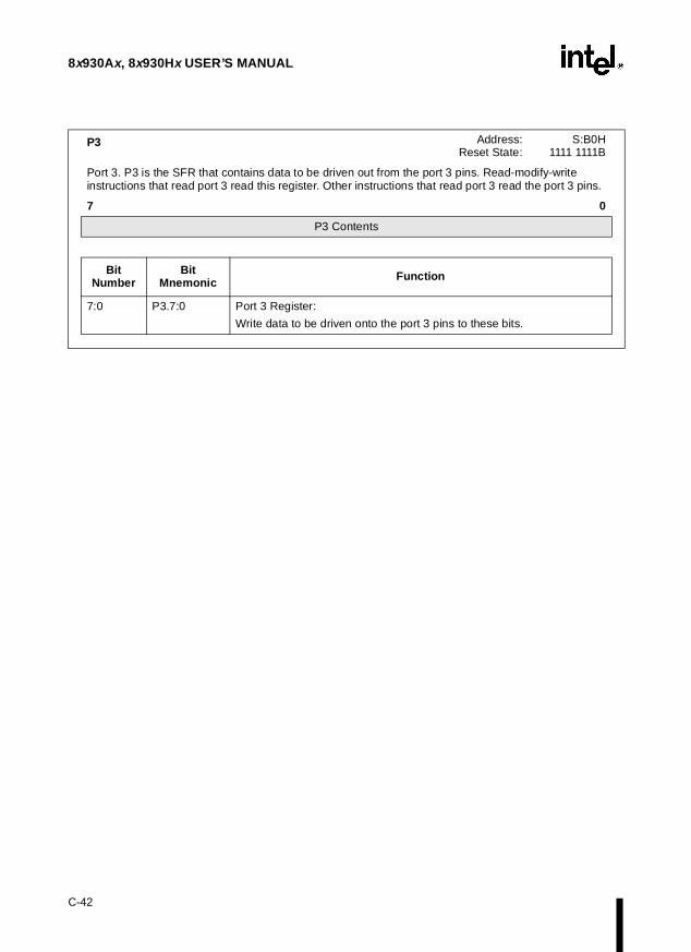
8x930Ax, 8x930Hx USER’S MANUAL
P3 Address: S:B0HReset State: 1111 1111B
Port 3. P3 is the SFR that contains data to be driven out from the port 3 pins. Read-modify-write instructions that read port 3 read this register. Other instructions that read port 3 read the port 3 pins.
7 0
P3 Contents
Bit Number
Bit Mnemonic Function
7:0 P3.7:0 Port 3 Register:
Write data to be driven onto the port 3 pins to these bits.
C-42

REGISTERS
PCON Address: S:87HReset State: 00xx 0000B
Power Control Register. Contains the power off flag (POF) and bits for enabling the idle and powerdown modes. Also contains two general-purpose flags and two bits that control serial I/O functions—the double baud rate bit and a bit that selects whether accesses to SCON.7 are to the FE bit or the SM0 bit.
7 0
SMOD1 SMOD0 LC POF GF1 GF0 PD IDL
Bit Number
Bit Mnemonic Function
7 SMOD1 Double Baud Rate Bit:
When set, doubles the baud rate when timer 1 is used and mode 1, 2, or 3 is selected in the SCON register. See “Baud Rates” on page 13-10.
6 SMOD0 SCON.7 Select:
When set, read/write accesses to SCON.7 are to the FE bit.When clear, read/write accesses to SCON.7 are to the SM0 bit.See the SCON register (Figure 13-2 on page 13-4).
5 LC Low-clock Mode Enable:
Setting this bit forces the internal clock (FCLK) distributed to the CPU and peripherals (but not the USB module) to 3 MHz. This bit is automatically set after a reset. Clearing this bit through firmware returns FCLK to the clock frequency determined by pins PLLSEL2:0.
4 POF Power Off Flag:
Set by hardware as VCC rises above 3 V to indicate that power has been off or VCC had fallen below 3 V and that on-chip volatile memory is indeterminate. Set or cleared by firmware.
3 GF1 General Purpose Flag:
Set or cleared by firmware. One use is to indicate whether an interrupt occurred during normal operation or during idle mode.
2 GF0 General Purpose Flag:
Set or cleared by firmware. One use is to indicate whether an interrupt occurred during normal operation or during idle mode.
1 PD Powerdown Mode Bit:
When set, activates powerdown mode. This bit should only be set if the GSUS bit is also set. Cleared by hardware when an interrupt or reset occurs.
0 IDL Idle Mode Bit:
When set, activates idle mode. Cleared by hardware when an interrupt or reset occurs.If IDL and PD are both set, PD takes precedence.
C-43

8x930Ax, 8x930Hx USER’S MANUAL
PCON1 Address: S:0DFHReset State: xxx0 0000B
USB Power Control Register. Facilitates the control and status relating to global suspend and resume, USB reset separation, and remote wake-up of the 8x930.
7 0
— — — URDIS URST RWU GRSM GSUS
Bit Number
Bit Mnemonic Function
7:5 — Reserved:
The value read from these bits are indeterminate. Write zeroes to these bits.
4 URDIS(8x930Ax)
USB Reset Disable:
When clear by firmware, a chip reset occurs upon receiving of a USB reset signal. This resets the MCS® 251 core, USB blocks and all peripherals.
When set by firmware, the MCS 251 core and peripherals will not reset when a USB reset signal is detected. Upon detecting a USB reset signal, the 8x930Ax resets all the USB blocks (FIFOs, FIU, SIE, and transceiver), sets the URST bit and generates a USB reset interrupt (refer to the description of URST).
URDIS(8X930Hx)
Reserved:
The value read from these bits are indeterminate. Write zeroes to these bits.
3 URST(8x930Ax)
USB Reset Flag:
This flag will be set by hardware when a USB reset occurs, regardless of whether the ESR bit in the IEN1 register is enabled or disabled. The URST also serves as the interrupt bit, ORed with GRSM and GSUS bits to generate an interrupt. Should be cleared by firmware when serving the USB reset interrupt.
URST(8x930Hx)
Reserved:
The value read from these bits are indeterminate. Write zeroes to these bits.
2 RWU Remote Wake-up Bit:
1 = wake-up. This bit is used by the USB function to initiate a remote wake-up. Set by firmware to drive resume signaling on the USB lines to the host or upstream hub. Cleared by hardware. Note: do not set this bit unless the USB function is suspended (GSUS = 1 and GRSM = 0). See Figure 15-3 on page 15-11.
† Firmware should prioritize GRSM over GSUS if both bits are set simultaneously.
C-44

REGISTERS
1 GRSM Global Resume Bit:
1 = resume. Set by hardware when a global resume is detected on the USB lines. This bit is ORed with GSUS to generate the interrupt† Cleared by firmware when servicing the global suspend/resume interrupt. (This bit can also be set/cleared by firmware for testability.) This bit is not set if remote wakeup is used (see RWU). See Figure 15-3 on page 15-11.
0 GSUS Global Suspend Bit:
1 = suspend. This bit is set by hardware when global suspend is detected on the USB lines. This bit is ORed with the GRSM bit to generate the interrupt.† During this ISR, firmware should set the PD bit to enter the suspend mode. Cleared by firmware when a resume occurs. See Figure 15-3 on page 15-11.
PCON1 (Continued) Address: S:0DFHReset State: xxx0 0000B
USB Power Control Register. Facilitates the control and status relating to global suspend and resume, USB reset separation, and remote wake-up of the 8x930.
7 0
— — — URDIS URST RWU GRSM GSUS
† Firmware should prioritize GRSM over GSUS if both bits are set simultaneously.
C-45

8x930Ax, 8x930Hx USER’S MANUAL
.
PSW Address: S:D0HReset State: 0000 0000B
7 0
CY AC F0 RS1 RS0 OV UD P
Bit Number
Bit Mnemonic Function
7 CY Carry Flag:
The carry flag is set by an addition instruction (ADD, ADDC) if there is a carry out of the MSB. It is set by a subtraction (SUB, SUBB) or compare (CMP) if a borrow is needed for the MSB. The carry flag is also affected by logical bit, bit move, multiply, decimal adjust, and some rotate and shift instructions (see Table 5-10).
6 AC Auxiliary Carry Flag:
The auxiliary carry flag is affected only by instructions that address 8-bit operands. The AC flag is set if an arithmetic instruction with an 8-bit operand produces a carry out of bit 3 (from addition) or a borrow into bit 3 (from subtraction). Otherwise, it is cleared. This flag is useful for BCD arithmetic (see Table 5-10).
5 F0 Flag 0:
This general-purpose flag is available to the user.
4:3 RS1:0 Register Bank Select Bits 1 and 0:
These bits select the memory locations that comprise the active bank of the register file (registers R0–R7).
RS1 RS0 Bank Address
0 0 0 00H–07H0 1 1 08H–0FH1 0 2 10H–17H1 1 3 18H–1FH
2 OV Overflow Flag:
This bit is set if an addition or subtraction of signed variables results in an overflow error (i.e., if the magnitude of the sum or difference is too great for the seven LSBs in 2’s-complement representation). The overflow flag is also set if a multiplication product overflows one byte or if a division by zero is attempted.
1 UD User-definable Flag:
This general-purpose flag is available to the user.
0 P Parity Bit:
This bit indicates the parity of the accumulator. It is set if an odd number of bits in the accumulator are set. Otherwise, it is cleared. Not all instructions update the parity bit. The parity bit is set or cleared by instructions that change the contents of the accumulator (ACC, Register R11).
C-46
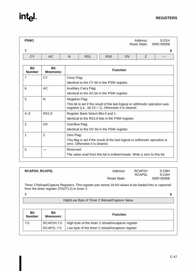
REGISTERS
.
PSW1 Address: S:D1HReset State: 0000 0000B
7 0
CY AC N RS1 RS0 OV Z —
Bit Number
Bit Mnemonic Function
7 CY Carry Flag:
Identical to the CY bit in the PSW register.
6 AC Auxiliary Carry Flag:
Identical to the AC bit in the PSW register.
5 N Negative Flag:
This bit is set if the result of the last logical or arithmetic operation was negative (i.e., bit 15 = 1). Otherwise it is cleared.
4–3 RS1:0 Register Bank Select Bits 0 and 1:
Identical to the RS1:0 bits in the PSW register.
2 OV Overflow Flag:
Identical to the OV bit in the PSW register.
1 Z Zero Flag:
This flag is set if the result of the last logical or arithmetic operation is zero. Otherwise it is cleared.
0 — Reserved:
The value read from this bit is indeterminate. Write a zero to this bit.
RCAP2H, RCAP2L Address: RCAP2H S:CBHRCAP2L S:CAH
Reset State: 0000 0000B
Timer 2 Reload/Capture Registers. This register pair stores 16-bit values to be loaded into or captured from the timer register (TH2/TL2) in timer 2.
7 0
High/Low Byte of Timer 2 Reload/Capture Value
Bit Number
Bit Mnemonic Function
7:0 RCAP2H.7:0
RCAP2L.7:0
High byte of the timer 2 reload/recapture register
Low byte of the timer 2 reload/recapture register
C-47

8x930Ax, 8x930Hx USER’S MANUAL
RXCNTH, RXCNTL(Endpoint-indexed)
Address: S:E7H S:E6H
Reset States:Endpoint 1 RXCNTH xxxx xx00B
RXCNTL 0000 0000BOther
Endpoints† RXCNTL xxx0 0000B
Receive FIFO Byte-count High and Low Registers. High and low register in a two-register ring buffer used to store the byte count for the data packets received in the receive FIFO specified by EPINDEX.
15 (RXCNT) Endpoint 1 8
— — — — — — BC9 BC8
7 (RXCNTL) 0
BC7 BC6 BC5 BC4 BC3 BC2 BC1 BC0
7 (RXCNTL) Other Endpoints† 0
— — — BC4 BC3 BC2 BC1 BC0
Bit Number
Bit Mnemonic Function
Endpoint 1
15:10 — Reserved. Write zeros to these bits.
9:0 BC9:0 Receive Byte Count.Ten-bit, ring buffer byte. Stores receive byte count (RXCNT). Implemented for function endpoint 1 only.
Other Endpoints†
7:0 — Reserved. Write zeros to these bits.
4:0 BC4:0 Receive Byte Count.Five-bit, ring buffer. Stores receive byte count (RXCNT). 3.
† Other endpoints = Hub endpoint 0; function endpoints 0, 3:2 or 0, 5:2 (6EPP option, 8x930Ax only). Byte count registers are not implemented for hub endpoint 1.
C-48

REGISTERS
RXCON(Endpoint-indexed)
Address: S:E4HReset State: 0x00 0100B
Receive FIFO Control Register. Controls the receive FIFO specified by EPINDEX.
7 0
RXCLR — RXWS RXFFRC RXISO ARM ADVWM REVWP
Bit Number
Bit Mnemonic Function
7 RXCLR Clear the Receive FIFO:
Set this bit to flush the entire receive FIFO. All flags in RXFLG revert to their reset states (RXEMP is set; all other flags clear). The ARM, RXISO and RXWS bits in this register and the RXSEQ bit in the RXSTAT register are not affected by this operation. Hardware clears this bit when the flush operation is completed.
6 — Reserved:
Values read from this bit are indeterminate. Write zero to this bit.
5 RXWS Receive FIFO Wait-state Read:
At the 8x930 core frequency of 12 MHz, not all instructions that access the receive FIFO are guaranteed to work due to critical paths inherent in the 8x930 architecture.While all MOV instructions from the receive FIFO are guaranteed to work at 12 MHz, arithmetic instructions (e.g., ADD, SUB, etc.) where the receive FIFO is the source and the register file the destination may not work at this speed. For applications using arithmetic instructions, set the RXWS bit to read the receive FIFO with one wait state — this will eliminate the critical path. This bit is not reset when the RXCLR bit is set.
4 RXFFRC FIFO Read Complete:†
Set this bit to release the receive FIFO when a data set read is complete. Setting this bit “clears” the RXFIF “bit” (in the RXFLG register) corresponding to the data set that was just read. Hardware clears this bit after the RXFIF bit is cleared. All data from this data set must have been read. Note that FIFO Read Complete only works if STOVW and EDOVW are cleared.
3 RXISO Isochronous Data Type:†
Set this bit to indicate that the receive FIFO is programmed to receive isochronous data and to set up the USB Interface to handle an isochronous data transfer. This bit is not reset when the RXCLR bit is set; it must be cleared by firmware.
† ARM mode is recommended. ADVWM and REVWP, which control the write marker and write pointer when ARM = 0, are used for test purposes,
C-49

8x930Ax, 8x930Hx USER’S MANUAL
2 ARM Auto Receive Management:
When set, the write pointer and write marker are adjusted automatically based on the following conditions:
RXISO RX Status Write Pointer Write Marker
X ACK Unchanged Advanced
0 NAK Reversed Unchanged
1 NAK Unchanged Advanced
When this bit is set, setting REVWP or ADVWM has no effect. Hardware neither clears nor sets this bit. This is a sticky bit that is not reset when RXCLR is set.NOTE: This bit should always be set, except for testing.
1 ADVWM Advance Write Marker: †
(For non-ARM mode only) Set this bit to advance the write marker to the origin of the next data set. Advancing the write marker is used for back-to-back receptions. Hardware clears this bit after the write marker is advanced. Setting this bit is effective only when the REVWP, ARM and RXCLR bits are clear.
0 REVWP Reverse Write Pointer: †
(For non-ARM mode only) Set this bit to return the write pointer to the origin of the last data set received, as identified by the write marker. The FIU can then re-receive the last data packet and write to the receive FIFO starting from the same origin when the host re-sends the same data packet. Hardware clears this bit after the write pointer is reversed. Setting this bit is effective only when the ADVWM, ARM, and RXCLR bits are all clear.
REVWP is used when a data packet is bad. When the function interface receives the data packet again, the write starts at the origin of the previous (bad) data set.
RXCON (Continued)(Endpoint-indexed)
Address: S:E4HReset State: 0x00 0100B
Receive FIFO Control Register. Controls the receive FIFO specified by EPINDEX.
7 0
RXCLR — RXWS RXFFRC RXISO ARM ADVWM REVWP
Bit Number
Bit Mnemonic Function
† ARM mode is recommended. ADVWM and REVWP, which control the write marker and write pointer when ARM = 0, are used for test purposes,
C-50
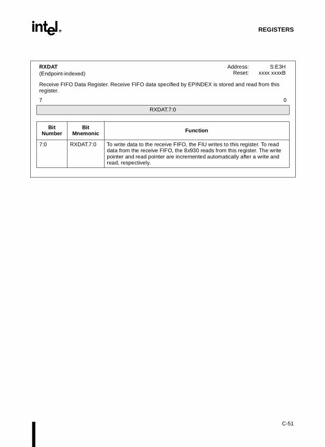
REGISTERS
RXDAT(Endpoint-indexed)
Address: S:E3HReset: xxxx xxxxB
Receive FIFO Data Register. Receive FIFO data specified by EPINDEX is stored and read from this register.
7 0
RXDAT.7:0
Bit Number
Bit Mnemonic Function
7:0 RXDAT.7:0 To write data to the receive FIFO, the FIU writes to this register. To read data from the receive FIFO, the 8x930 reads from this register. The write pointer and read pointer are incremented automatically after a write and read, respectively.
C-51

8x930Ax, 8x930Hx USER’S MANUAL
RXFLG (Endpoint-indexed)
Address: S:E5HReset State: 00xx 1000B
Receive FIFO Flag Register. These flags indicate the status of data packets in the receive FIFO specified by EPINDEX.
7 0
RXFIF1 RXFIF0 — — RXEMP RXFULL RXURF RXOVF
Bit Number
Bit Mnemonic Function
7:6 RXFIF1:0 Receive FIFO Index Flags: (read-only)
These read-only flags indicate which data packets are present in the receive FIFO (see Table 7-5 on page 7-26). The RXFIF bits are updated after each write to RXCNT to reflect the addition of a data packet. Likewise, the RXFIF bits are cleared in sequence after each setting of the RXFFRC bit. The next-state table for RXFIF bits is shown below for operation in dual packet mode.
RXFIF1:0 Operation Flag Next RXFIF1:0 Next Flag
00 Adv WM X 01 Unchanged01 Adv WM X 01 Unchanged10 Adv WM X 11 Unchanged
00 Set RXFFRC X 00 Unchanged01 Set RXFFRC X 00 Unchanged11 Set RXFFRC X 10/01 Unchanged10 Set RXFFRC X 00 Unchanged
XX Rev WP X Unchanged Unchanged
When the receive FIFO is programmed to operate in single packet mode (RXSPM set in EPCON), valid RXFIF states are 00 and 01 only.
In ISO mode, RXOVF, RXURF, and RXFIF are handled using the following rule: Firmware events cause status change immediately, while USB events cause status change only at SOF. RXFIF is “incremented” by the USB and “decremented” by firmware.Therefore, setting RXFFRC “decrements” RXFIF immediately. However, a successful USB transaction within a frame “increments” RXFIF only at SOF. For traceability, you must check the RXFIF flags before and after reads from the receive FIFO and the setting of RXFFRC in RXCON.NOTE: To simplify firmware development, it is recommended that you
utilize control endpoints in single-packet mode only.
5:4 — Reserved:Values read from these bits are indeterminate. Write zeros to these bits.
3 RXEMP Receive FIFO Empty Flag (read-only):
Hardware sets this flag when the write pointer is at the same location as the read pointer and the write pointer equals the write marker and neither pointer has rolled over. Hardware clears the bit when the empty condition no longer exists. This is not a sticky bit and always tracks the current status of the receive FIFO, regardless of ISO or non-ISO mode.
† When set, all transmissions are NAKed.
C-52

REGISTERS
2 RXFULL Receive FIFO Full Flag (read-only):
Hardware sets this flag when the write pointer has rolled over and equals the read pointer. Hardware clears the bit when the full condition no longer exists. This is not a sticky bit and always tracks the current status of the receive FIFO, regardless of ISO or non-ISO mode.
1 RXURF Receive FIFO Underrun Flag†:
Hardware sets this bit when an additional byte is read from an empty receive FIFO or RXCNT. Hardware does not clear this bit, so you must clear it in firmware. When the receive FIFO underruns, the read pointer will not advance — it remains locked in the empty position.
In ISO mode, RXOVF, RXURF, and RXFIF are handled using the following rule: Firmware events cause status change immediately, while USB events cause status change only at SOF. Since underrun can only be caused by firmware, RXURF is updated immediately. You must check the RXURF flag after reads from the receive FIFO before setting the RXFFRC bit in RXCON.NOTE: When this bit is set, the FIFO is in an unknown state. It is
recommended that you reset the FIFO in the error management routine using the RXCLR bit in the RXCON register.
0 RXOVF Receive FIFO Overrun Flag†:
This bit is set when the FIU writes an additional byte to a full receive FIFO or writes a byte count to RXCNT with FIF1:0 = 11. This is a sticky bit that must be cleared through firmware, although it can be cleared by hardware if a SETUP packet is received after an RXOVF error had already occurred.†
When this bit is set, the FIFO is in an unknown state, thus it is recommended that you reset the FIFO in the error management routine using the RXCLR bit in the RXCON register. When the receive FIFO overruns, the write pointer will not advance — it remains locked in the full position.
In ISO mode, RXOVF, RXURF, and RXFIF are handled using the following rule: Firmware events cause status change immediately, while USB events cause status change only at SOF. Since overrun can only be caused by the USB, RXOVF is updated only at the next SOF regardless of where the overrun occurred during the current frame.†
RXFLG (Continued) (Endpoint-indexed)
Address: S:E5HReset State: 00xx 1000B
Receive FIFO Flag Register. These flags indicate the status of data packets in the receive FIFO specified by EPINDEX.
7 0
RXFIF1 RXFIF0 — — RXEMP RXFULL RXURF RXOVF
Bit Number
Bit Mnemonic Function
† When set, all transmissions are NAKed.
C-53

8x930Ax, 8x930Hx USER’S MANUAL
RXSTAT (Endpoint-indexed)
Address: S:E2H Reset State: 0000 0000B
Endpoint Receive Status Register. Contains the current endpoint status of the receive FIFO specified by EPINDEX. (Endpoint-indexed SFR)
7 0
RXSEQ RXSETUP STOVW EDOVW RXSOVW RXVOID RXERR RXACK
Bit Number
Bit Mnemonic Function
7 RXSEQ Receiver Endpoint Sequence Bit (read, conditional write): †
This bit will be toggled on completion of an ACK handshake in response to an OUT token. This bit will be set (or cleared) by hardware after reception of a SETUP token.
This bit can be written by firmware if the RXSOVW bit is set when written along with the new RXSEQ value.NOTE: Always verify this bit after writing to ensure that there is no conflict
with hardware, which could occur if a new SETUP token is received.
6 RXSETUP Received Setup Token:
This bit is set by hardware when a valid SETUP token has been received. When set, this bit causes received IN or OUT tokens to be NAKed until the bit is cleared to allow proper data management for the transmit and receive FIFOs from the previous transaction.
IN or OUT tokens are NAKed even if the endpoint is stalled (RXSTL or TXSTL) to allow a control transaction to clear a stalled endpoint.
Clear this bit upon detection of a SETUP token after the firmware is ready to complete the status stage of a control transaction.
5 STOVW Start Overwrite Flag (read-only):
Set by hardware upon receipt of a SETUP token for any control endpoint to indicate that the receive FIFO is being overwritten with new SETUP data. When set, the FIFO state (FIF and read pointer) resets and is locked for this endpoint until EDOVW is set. This prevents a prior, ongoing firmware read from corrupting the read pointer as the receive FIFO is being cleared and new data is being written into it. This bit is cleared by hardware at the end of handshake phase transmission of the setup stage.
This bit is used only for control endpoints.† Under normal operation, this bit should not be modified by the user.†† For additional information on the operation of these bits see Appendix D, “Data Flow Model.”††† The SIE will handle all sequence bit tracking. This bit should be used only when initializing a new
configuration or interface.
C-54

REGISTERS
4 EDOVW End Overwrite Flag:† This flag is set by hardware during the handshake phase of a SETUP stage. It is set after every SETUP packet is received and must be cleared prior to reading the contents of the FIFO. When set, the FIFO state (FIF and read pointer) remains locked for this endpoint until this bit is cleared. This prevents a prior, ongoing firmware read from corrupting the read pointer after the new data has been written into the receive FIFO.
This bit is only used for control endpoints.NOTE: Make sure the EDOVW bit is cleared prior to reading the contents
of the FIFO.
3 RXSOVW Receive Data Sequence Overwrite Bit: †
Write a ‘1’ to this bit to allow the value of the RXSEQ bit to be overwritten. Writing a ‘0’ to this bit has no effect on RXSEQ. This bit always returns ‘0’ when read. †††
2 RXVOID Receive Void Condition (read-only):††
This bit is set when no valid data is received in response to a SETUP or OUT token due to one of the following conditions:
1. The receive FIFO is still locked
2. The EPCON register’s RXSTL bit is set
This bit is set and cleared by hardware. For non-isochronous transactions, this bit is updated by hardware at the end of the transaction in response to a valid OUT token. For isochronous transactions, it is not updated until the next SOF.
RXSTAT (Endpoint-indexed)
Address: S:E2H Reset State: 0000 0000B
Endpoint Receive Status Register. Contains the current endpoint status of the receive FIFO specified by EPINDEX. (Endpoint-indexed SFR)
7 0
RXSEQ RXSETUP STOVW EDOVW RXSOVW RXVOID RXERR RXACK
Bit Number
Bit Mnemonic Function
† Under normal operation, this bit should not be modified by the user.†† For additional information on the operation of these bits see Appendix D, “Data Flow Model.”††† The SIE will handle all sequence bit tracking. This bit should be used only when initializing a new
configuration or interface.
C-55

8x930Ax, 8x930Hx USER’S MANUAL
1 RXERR Receive Error (read-only):††
Set when an error condition has occurred with the reception. Complete or partial data has been written into the receive FIFO. No handshake is returned. The error can be one of the following conditions:
1. Data failed CRC check.
2. Bit stuffing error.
3. A receive FIFO goes into overrun or underrun condition while receiving.
This bit is updated by hardware at the end of a valid SETUP or OUT token transaction (non-isochronous) or at the next SOF on each valid OUT token transaction (isochronous).
The corresponding FRXDx bit of FIFLG or FIFLG1 (8x930Ax with 6EPP) is set when active. This bit is updated with the RXACK bit at the end of data reception and is mutually exclusive with RXACK.
0 RXACK Receive Acknowledged (read-only):††
This bit is set when data is received completely into a receive FIFO and an ACK handshake is sent. This read-only bit is updated by hardware at the end of a valid SETUP or OUT token transaction (non-isochronous) or at the next SOF on each valid OUT token transaction (isochronous).
The corresponding FRXDx bit of FIFLG or FIFLG1 (8x930Ax with 6EPP) is set when active. This bit is updated with the RXERR bit at the end of data reception and is mutually exclusive with RXERR.
RXSTAT (Endpoint-indexed)
Address: S:E2H Reset State: 0000 0000B
Endpoint Receive Status Register. Contains the current endpoint status of the receive FIFO specified by EPINDEX. (Endpoint-indexed SFR)
7 0
RXSEQ RXSETUP STOVW EDOVW RXSOVW RXVOID RXERR RXACK
Bit Number
Bit Mnemonic Function
† Under normal operation, this bit should not be modified by the user.†† For additional information on the operation of these bits see Appendix D, “Data Flow Model.”††† The SIE will handle all sequence bit tracking. This bit should be used only when initializing a new
configuration or interface.
C-56

REGISTERS
SADDR Address: S:A9HReset State: 0000 0000B
Slave Individual Address Register. SADDR contains the device’s individual address for multiprocessor communication.
7 0
Slave Individual Address
Bit Number
Bit Mnemonic Function
7:0 SADDR.7:0
SADEN Address: S:B9HReset State: 0000 0000B
Mask Byte Register. This register masks bits in the SADDR register to form the device’s given address for multiprocessor communication.
7 0
Mask for SADDR
Bit Number
Bit Mnemonic Function
7:0 SADEN.7:0
SBUF Address: S:99HReset State: xxxx xxxxB
Serial Data Buffer. Writing to SBUF loads the transmit buffer of the serial I/O port. Reading SBUF reads the receive buffer of the serial I/O port.
7 0
Data Sent/Received by Serial I/O Port
Bit Number
Bit Mnemonic Function
7:0 SBUF.7:0
C-57

8x930Ax, 8x930Hx USER’S MANUAL
SCON Address: S:98HReset State: 0000 0000B
Serial Port Control Register. SCON contains serial I/O control and status bits, including the mode select bits and the interrupt flag bits.
7 0
FE/SM0 SM1 SM2 REN TB8 RB8 TI RI
Bit Number
Bit Mnemonic Function
7 FE
SM0
Framing Error Bit:
To select this function, set the SMOD0 bit in the PCON register. Set by hardware to indicate an invalid stop bit. Cleared by firmware, not by valid frames.
Serial Port Mode Bit 0:
To select this function, clear the SMOD0 bit in the PCON register. Firmware writes to bits SM0 and SM1 to select the serial port operating mode. Refer to the SM1 bit for the mode selections.
6 SM1 Serial Port Mode Bit 1:
Firmware writes to bits SM1 and SM0 (above) to select the serial port operating mode.
SM0 SM1 Mode Description Baud Rat e†
0 0 0 Shift register FCLK/60 1 1 8-bit UART Variable1 0 2 9-bit UART FCLK/16†† or FCLK/32††
1 1 3 9-bit UART Variable†See note on page page 13-1.††Select by programming the SMOD bit in the PCON register (see section “Baud Rates” on page 13-10).
5 SM2 Serial Port Mode Bit 2:
Firmware writes to bit SM2 to enable and disable the multiprocessor communication and automatic address recognition features. This allows the serial port to differentiate between data and command frames and to recognize slave and broadcast addresses.
4 REN Receiver Enable Bit:
To enable reception, set this bit. To enable transmission, clear this bit.
3 TB8 Transmit Bit 8:
In modes 2 and 3, firmware writes the ninth data bit to be transmitted to TB8. Not used in modes 0 and 1.
C-58

REGISTERS
2 RB8 Receiver Bit 8:
Mode 0: Not used.
Mode 1 (SM2 clear): Set or cleared by hardware to reflect the stop bit received.
Modes 2 and 3 (SM2 set): Set or cleared by hardware to reflect the ninth data bit received.
1 TI Transmit Interrupt Flag Bit:
Set by the transmitter after the last data bit is transmitted. Cleared by firmware.
0 RI Receive Interrupt Flag Bit:
Set by the receiver after the last data bit of a frame has been received. Cleared by firmware.
SCON (Continued) Address: S:98HReset State: 0000 0000B
Serial Port Control Register. SCON contains serial I/O control and status bits, including the mode select bits and the interrupt flag bits.
7 0
FE/SM0 SM1 SM2 REN TB8 RB8 TI RI
Bit Number
Bit Mnemonic Function
C-59

8x930Ax, 8x930Hx USER’S MANUAL
SOFH Address: S:D3HReset State: 0000 0000B
Start of Frame High Register. Contains isochronous data transfer enable and interrupt bits and the upper three bits of the 11-bit time stamp received from the host.
7 0
SOFACK ASOF SOFIE FTLOCK SOFODIS TS10 TS9 TS8
Bit Number
Bit Mnemonic Function
7 SOFACK SOF Token Received without Error (read-only):
When set, this bit indicates that the 11-bit time stamp stored in SOFL and SOFH is valid. This bit is updated every time a SOF token is received from the USB bus, and it is cleared when an artificial SOF is generated by the frame timer. This bit is set and cleared by hardware.
6 ASOF Any Start of Frame:
This bit is set by hardware to indicate that a new frame has started. The interrupt can result either from reception of an actual SOF packet or from an artificially-generated SOF from the frame timer. This interrupt is asserted in hardware even if the frame timer is not locked to the USB bus frame timing. When set, this bit is an indication that either an actual SOF packet was received or an artificial SOF was generated by the frame timer. This bit must be cleared by firmware or inverted and driven to the SOF# pin. The effect of setting this bit by firmware is the same as hardware: the external pin will be driven with an inverted ASOF value for eight TCLKs.
This bit also serves as the SOF interrupt flag. This interrupt is only asserted in hardware if the SOF interrupt is enabled (SOFIE set) and the interrupt channel is enabled.
5 SOFIE SOF Interrupt Enable:
When this bit is set, setting the ASOF bit causes an interrupt request to be generated if the interrupt channel is enabled. Hardware reads but does not write this bit.
4 FTLOCK Frame Timer Locked (read-only):
When set, this bit indicates that the frame timer is presently locked to the USB bus’ frame time. When cleared, this bit indicates that the frame timer is attempting to synchronize to the frame time.
3 SOFODIS SOF# Pin Output Disable:
When set, no low pulse will be driven to the SOF# pin in response to setting the ASOF bit. The SOF# pin will be driven to ‘1’ when SOFODIS is set. When this bit is clear, setting the ASOF bit causes the SOF# pin to be toggled with a low pulse for eight TCLKs.
2:0 TS10:8 Time stamp received from host:
TS10:8 are the upper three bits of the 11-bit frame number issued with an SOF token. This time stamp is valid only if the SOFACK bit is set.
C-60

REGISTERS
SOFL Address: S:D2HReset State: 0000 0000B
Start-of-Frame Low Register. Contains the lower eight bits of the 11-bit time stamp received from the host.
7 0
TS7:0
Bit Number
Bit Mnemonic Function
7:0 TS7:0 Time stamp received from host:
This time stamp is valid only if the SOFACK bit in the SOFH register is set. TS7:0 are the lower eight bits of the 11-bit frame number issued with a SOF token. If an artificial SOF is generated, the time stamp remains at its previous value and it is up to firmware to update it. These bits are set and cleared by hardware.
SP Address: S:81HReset State: 0000 0111B
Stack Pointer. SP provides SFR access to location 63 in the register file (also named SP). SP is the lowest byte of the extended stack pointer (SPX = DR60). The extended stack pointer points to the current top of stack. When a byte is saved (PUSHed) on the stack, SPX is incremented, and then the byte is written to the top of stack. When a byte is retrieved (POPped) from the stack, it is copied from the top of stack, and then SPX is decremented.
7 0
SP Contents
Bit Number
Bit Mnemonic Function
7:0 SP.7:0 Stack Pointer:
Bits 0–7 of the extended stack pointer, SPX (DR60).
C-61

8x930Ax, 8x930Hx USER’S MANUAL
SPH Address: S:BEHReset State: 0000 0000B
Stack Pointer High. SPH provides SFR access to location 62 in the register file (also named SPH). SPH is the upper byte of the lower word of DR60, the extended stack pointer (SPX). The extended stack pointer points to the current top of stack. When a byte is saved (PUSHed) on the stack, SPX is incremented, and then the byte is written to the top of stack. When a byte is retrieved (POPped) from the stack, it is copied from the top of stack, and then SPX is decremented.
7 0
SPH Contents
Bit Number
Bit Mnemonic Function
7:0 SPH.7:0 Stack Pointer High:
Bits 8–15 of the extended stack pointer, SPX (DR(60)).
C-62

REGISTERS
T2CON Address: S:C8HReset State: 0000 0000B
Timer 2 Control Register. Contains the receive clock, transmit clock, and capture/reload bits used to configure timer 2. Also contains the run control bit, counter/timer select bit, overflow flag, external flag, and external enable for timer 2.
7 0
TF2 EXF2 RCLK TCLK EXEN2 TR2 C/T2# CP/RL2#
Bit Number
Bit Mnemonic Function
7 TF2 Timer 2 Overflow Flag:
Set by timer 2 overflow. Must be cleared by firmware. TF2 is not set if RCLK = 1 or TCLK = 1.
6 EXF2 Timer 2 External Flag:
If EXEN2 = 1, capture or reload caused by a negative transition on T2EX sets EFX2. EXF2 does not cause an interrupt in up/down counter mode (DCEN = 1).
5 RCLK Receive Clock Bit:
Selects timer 2 overflow pulses (RCLK = 1) or timer 1 overflow pulses (RCLK = 0) as the baud rate generator for serial port modes 1 and 3.
4 TCLK Transmit Clock Bit:
Selects timer 2 overflow pulses (TCLK = 1) or timer 1 overflow pulses (TCLK = 0) as the baud rate generator for serial port modes 1 and 3.
3 EXEN2 Timer 2 External Enable Bit:
Setting EXEN2 causes a capture or reload to occur as a result of a negative transition on T2EX unless timer 2 is being used as the baud rate generator for the serial port. Clearing EXEN2 causes timer 2 to ignore events at T2EX.
2 TR2 Timer 2 Run Control Bit:
Setting this bit starts the timer.
1 C/T2# Timer 2 Counter/Timer Select:
C/T2# = 0 selects timer operation: timer 2 counts the divided-down system clock. C/T2# = 1 selects counter operation: timer 2 counts negative transitions on external pin T2.
0 CP/RL2# Capture/Reload Bit:
When set, captures occur on negative transitions at T2EX if EXEN2 = 1. When cleared, auto-reloads occur on timer 2 overflows or negative transitions at T2EX if EXEN2 = 1. The CP/RL2# bit is ignored and timer 2 forced to auto-reload on timer 2 overflow, if RCLK = 1 or TCLK = 1.
C-63

8x930Ax, 8x930Hx USER’S MANUAL
T2MOD Address: S:C9HReset State: xxxx xx00B
Timer 2 Mode Control Register. Contains the timer 2 down count enable and clock-out enable bits for timer 2 .
7 0
— — — — — — T2OE DCEN
Bit Number
Bit Mnemonic Function
7:2 — Reserved:
Values read from these bits are indeterminate. Write zeros to these bits.
1 T2OE Timer 2 Output Enable Bit:
In the timer 2 clock-out mode, connects the programmable clock output to external pin T2.
0 DCEN Down Count Enable Bit:
Configures timer 2 as an up/down counter.
C-64
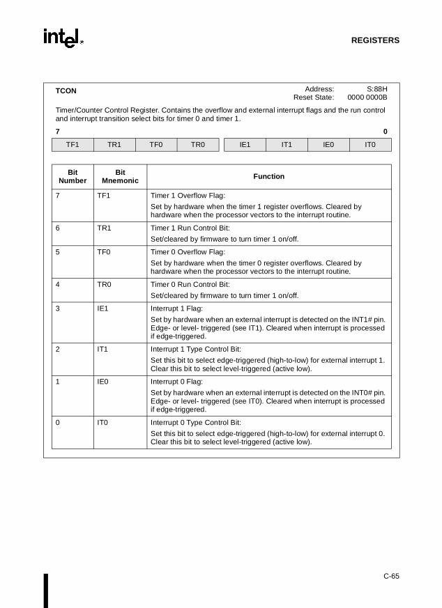
REGISTERS
TCON Address: S:88HReset State: 0000 0000B
Timer/Counter Control Register. Contains the overflow and external interrupt flags and the run control and interrupt transition select bits for timer 0 and timer 1.
7 0
TF1 TR1 TF0 TR0 IE1 IT1 IE0 IT0
Bit Number
Bit Mnemonic Function
7 TF1 Timer 1 Overflow Flag:
Set by hardware when the timer 1 register overflows. Cleared by hardware when the processor vectors to the interrupt routine.
6 TR1 Timer 1 Run Control Bit:
Set/cleared by firmware to turn timer 1 on/off.
5 TF0 Timer 0 Overflow Flag:
Set by hardware when the timer 0 register overflows. Cleared by hardware when the processor vectors to the interrupt routine.
4 TR0 Timer 0 Run Control Bit:
Set/cleared by firmware to turn timer 1 on/off.
3 IE1 Interrupt 1 Flag:
Set by hardware when an external interrupt is detected on the INT1# pin. Edge- or level- triggered (see IT1). Cleared when interrupt is processed if edge-triggered.
2 IT1 Interrupt 1 Type Control Bit:
Set this bit to select edge-triggered (high-to-low) for external interrupt 1.Clear this bit to select level-triggered (active low).
1 IE0 Interrupt 0 Flag:
Set by hardware when an external interrupt is detected on the INT0# pin. Edge- or level- triggered (see IT0). Cleared when interrupt is processed if edge-triggered.
0 IT0 Interrupt 0 Type Control Bit:
Set this bit to select edge-triggered (high-to-low) for external interrupt 0.Clear this bit to select level-triggered (active low).
C-65

8x930Ax, 8x930Hx USER’S MANUAL
TMOD Address: S:89HReset State: 0000 0000B
Timer/Counter Mode Control Register. Contains mode select, run control select, and counter/timer select bits for controlling timer 0 and timer 1.
7 0
GATE1 C/T1# M11 M01 GATE0 C/T0# M10 M00
Bit Number
Bit Mnemonic Function
7 GATE1 Timer 1 Gate:
When GATE1 = 0, run control bit TR1 gates the input signal to the timer register. When GATE1 = 1 and TR1 = 1, external signal INT1 gates the timer input.
6 C/T1# Timer 1 Counter/Timer Select:
C/T1# = 0 selects timer operation: timer 1 counts the divided-down system clock. C/T1# = 1 selects counter operation: timer 1 counts negative transitions on external pin T1.
5, 4 M11, M01 Timer 1 Mode Select:
M11 M010 0 Mode 0: 8-bit timer/counter (TH1) with 5-bit prescalar (TL1)0 1 Mode 1: 16-bit timer/counter1 0 Mode 2: 8-bit auto-reload timer/counter (TL1). Reloaded
from TH1 at overflow.1 1 Mode 3: Timer 1 halted. Retains count.
3 GATE0 Timer 0 Gate:
When GATE0 = 0, run control bit TR0 gates the input signal to the timer register. When GATE0 = 1 and TR0 = 1, external signal INT0 gates the timer input.
2 C/T0# Timer 0 Counter/Timer Select:
C/T0# = 0 selects timer operation: timer 0 counts the divided-down system clock. C/T0# = 1 selects counter operation: timer 0 counts negative transitions on external pin T0.
1, 0 M10, M00 Timer 0 Mode Select:
M10 M000 0 Mode 0: 8-bit timer/counter (T0) with 5-bit prescalar (TL0)0 1 Mode 1: 16-bit timer/counter1 0 Mode 2: 8-bit auto-reload timer/counter (TL0). Reloaded
from TH0 at overflow.1 1 Mode 3: TL0 is an 8-bit timer/counter. TH0 is an 8-bit
timer using timer 1’s TR1 and TF1 bits.
C-66
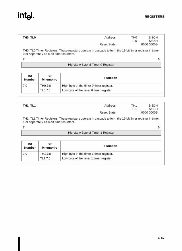
REGISTERS
TH0, TL0 Address: TH0 S:8CHTL0 S:8AH
Reset State: 0000 0000B
TH0, TL0 Timer Registers. These registers operate in cascade to form the 16-bit timer register in timer 0 or separately as 8-bit timer/counters.
7 0
High/Low Byte of Timer 0 Register
Bit Number
Bit Mnemonic Function
7:0 TH0.7:0
TL0.7:0
High byte of the timer 0 timer register.
Low byte of the timer 0 timer register.
TH1, TL1 Address: TH1 S:8DHTL1 S:8BH
Reset State: 0000 0000B
TH1, TL1 Timer Registers. These registers operate in cascade to form the 16-bit timer register in timer 1 or separately as 8-bit timer/counters.
7 0
High/Low Byte of Timer 1 Register
Bit Number
Bit Mnemonic Function
7:0 TH1.7:0
TL1.7:0
High byte of the timer 1 timer register.
Low byte of the timer 1 timer register.
C-67

8x930Ax, 8x930Hx USER’S MANUAL
TH2, TL2 Address: TH2 S:CDHTL2 S:CCH
Reset State: 0000 0000B
TH2, TL2 Timer Registers. These registers operate in cascade to form the 16-bit timer register in timer 2.
7 0
High/Low Byte of Timer 2 Register
Bit Number
Bit Mnemonic Function
7:0 TH2.7:0
TL2.7:0
High byte of the timer 2 timer register.
Low byte of the timer 2 timer register.
C-68
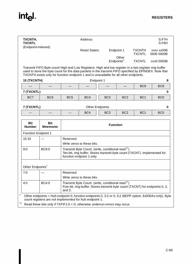
REGISTERS
TXCNTH,TXCNTL(Endpoint-indexed)
Address: S:F7HS:F6H
Reset States: Endpoint 1 TXCNTH xxxx xx00BTXCNTL 0000 0000B
OtherEndpoints† TXCNTL xxx0 0000B
Transmit FIFO Byte-count High and Low Registers. High and low register in a two-register ring buffer used to store the byte count for the data packets in the transmit FIFO specified by EPINDEX. Note that TXCNTH exists only for function endpoint 1 and is unavailable for all other endpoints.
15 (TXCNTH) Endpoint 1 8
— — — — — — BC9 BC8
7 (TXCNTL) 0
BC7 BC6 BC5 BC4 BC3 BC2 BC1 BC0
7 (TXCNTL) Other Endpoints 0
— — — BC4 BC3 BC2 BC1 BC0
Bit Number
Bit Mnemonic Function
Function Endpoint 1
15:10 — Reserved.
Write zeros to these bits.
9:0 BC9:0 Transmit Byte Count. (write, conditional read††)Ten-bit, ring buffer. Stores transmit byte count (TXCNT). Implemented for function endpoint 1 only.
Other Endpoints†
7:0 — Reserved.
Write zeros to these bits.
4:0 BC4:0 Transmit Byte Count. (write, conditional read††)Five-bit, ring buffer. Stores transmit byte count (TXCNT) for endpoints 0, 2, and 3.
† Other endpoints = Hub endpoint 0; function endpoints 0, 3:2 or 0, 5:2 (6EPP option, 8x930Ax only). Byte count registers are not implemented for hub endpoint 1.
†† Read these bits only if TXFIF1:0 = 0; otherwise underrun errors may occur.
C-69

8x930Ax, 8x930Hx USER’S MANUAL
TXCON(Endpoint-indexed)
Address: S:F4HReset State: Function Endpoint 1 000x 0100B
Other Endpoints† 0xxx 0100B
USB Transmit FIFO Control Register. Controls the transmit FIFO specified by EPINDEX.
7 0
Function Endpoint 1
TXCLR FFSZ1 FFSZ0 — TXISO ATM ADVRM REVRP
7 0
Other Endpoints †
TXCLR — — — TXISO ATM ADVRM REVRP
BitNumber
BitMnemonic Function
7 TXCLR Transmit Clear:
Setting this bit flushes the transmit FIFO, resets all the read/write pointers and markers, sets the EMPTY bit in TXFLG, and clears all other bits in TXFLG. After the flush, hardware clears this bit. Setting this bit does not affect the ATM, TXISO, and FFSZ bits, or the TXSEQ bit in the TXSTAT register.
6:5 FFSZ1:0
Function Endpoint 1 only
FIFO Size:
For function endpoint 1 only (EPINDEX = 0000 0001B), these bits select the sizes of both the transmit and receive FIFOs. (There are no FFSZ bits in the corresponding RXCON.) These bits are not reset when the TXCLR bit is set in the TXCON register.
FFSZ1:0 Transmit Size Receive Size
00 256 25601 512 51210 1024 011 0 1024
—
Other End-points †
Reserved:
Values read from this bit are indeterminate. Write zero to this bit.
4 — Reserved:
Values read from this bit are indeterminate. Write zero to this bit.
3 TXISO Transmit Isochronous Data:
Firmware sets this bit to indicate that the transmit FIFO contains isochronous data. The FIU uses this bit to set up the handshake protocol at the end of a transmission. This bit is not reset when TXCLR is set and must be cleared by firmware.
† Other endpoints = Hub endpoint 0; function endpoints 0, 3:2 or 0, 5:2 (for 6EPP option, 8x930Ax only).
†† ATM mode is recommended. ADVRM and REVRP, which control the read marker and read pointer when ATM = 0, are used for test purposes,
C-70

REGISTERS
2 ATM Automatic Transmit Management:
Setting this bit (the default value) causes the read pointer and read marker to be adjusted automatically as indicated:
TXISOTX Status Read Pointer Read Marker
X ACK Unchanged Advanced (1)0 NAK Reversed (2) Unchanged1 NAK Unchanged Advanced (1)
1. to origin of next data set 2. to origin of the data set last read
This bit should always be set, except for test purposes. Setting this bit disables ADVRM and REVRP. This is a sticky bit that is not reset when TXCLR is set, but can be set and cleared by firmware. Hardware neither clears nor sets this bit.
1 ADVRM Advance Read Marker Control (non-ATM mode only)††:
Setting this bit prepares for the next packet transmission by advancing the read marker to the origin of the next data packet (the position of the read pointer). Hardware clears this bit after the read marker is advanced. This bit is effective only when the REVRP, ATM, and TXCLR bits are all clear.
0 REVRP Reverse Read Pointer Control (non-ATM mode only)††:
In the case of a bad transmission, the same data stack may need to be available for retransmit. Setting this bit reverses the read pointer to point to the origin of the last data set (the position of the read marker) so that the FIU can reread the last set for retransmission. Hardware clears this bit after the read pointer is reversed. This bit is effective only when the ADVRM, ATM, and TXCLR bits are all clear.
TXCON (Continued)(Endpoint-indexed)
Address: S:F4HReset State: Function Endpoint 1 000x 0100B
Other Endpoints† 0xxx 0100B
USB Transmit FIFO Control Register. Controls the transmit FIFO specified by EPINDEX.
7 0
Function Endpoint 1
TXCLR FFSZ1 FFSZ0 — TXISO ATM ADVRM REVRP
7 0
Other Endpoints †
TXCLR — — — TXISO ATM ADVRM REVRP
BitNumber
BitMnemonic Function
† Other endpoints = Hub endpoint 0; function endpoints 0, 3:2 or 0, 5:2 (for 6EPP option, 8x930Ax only).
†† ATM mode is recommended. ADVRM and REVRP, which control the read marker and read pointer when ATM = 0, are used for test purposes,
C-71

8x930Ax, 8x930Hx USER’S MANUAL
TXDAT (Endpoint-indexed)†
Address: S:F3HReset State: xxxx xxxxB
USB Transmit FIFO Data Register. Data to be transmitted by the FIFO specified by EPINDEX is first written to this register.
7 0
Transmit Data Byte
Bit Number
Bit Mnemonic Function
7:0 TXDAT.7:0 Transmit Data Byte (write-only):
To write data to the transmit FIFO, write to this register. The write pointer is incremented automatically after a write.
† For hub endpoint 1, TXDAT is used in a different manner. See Figure 8-6 on page 8-12.
TXDAT (For hub endpoint 1 only) EPINDEX=81H† Address: S:F3HReset State: 0000 0000B
7 0
— — — TXDAT.4 TXDAT.3 TXDAT.2 TXDAT.1 TXDAT.0
Bit Number
Bit Mnemonic Function
7:5 — Reserved:
Values read from these bits are indeterminate.
4:0 TXDAT.4:0 Hub Endpoint 1 Status Change (read-only††):
Hardware communicates status changes to the host by setting the appropriate bit:
TXDAT.0 hub status changeTXDAT.1 port 1 status changeTXDAT.2 port 2 status changeTXDAT.3 port 3 status changeTXDAT.4 port 4 status change
A ‘1’ indicates a status change and ‘0’ indicates no status change. When endpoint 1 is addressed via an IN token, the entire byte is sent if at least one bit is a ‘1’. If all bits are zero, a NAK handshake is returned.
† TXDAT SFRs are also used for function (and hub endpoint 0) data transmission (EPINDEX=0xH or 80H). In that case, the bits are defined differently as shown in Figure 7-8 on page 7-18.
†† Bits 4-0 can be set indirectly by firmware by writing to port x’s HPSC SFR. Setting any bit in port x’s HPSC results in the hardware setting bit x in TXDAT. Bits can be cleared indirectly in firmware by clearing the condition that caused the status change.
C-72

REGISTERS
TXFLG(Endpoint-indexed)
Address: S:F5HReset State: 00xx 1000B
Transmit FIFO Flag Register. These flags indicate the status of data packets in the transmit FIFO specified by EPINDEX.
7 0
TXFIF1 TXFIF0 — — TXEMP TXFULL TXURF TXOVF
Bit Number
Bit Mnemonic Function
7:6 TXFIF1:0 FIFO Index Flags (read-only):
These flags indicate which data sets are present in the transmit FIFO. The FIF bits are set in sequence after each write to TXCNT to reflect the addition of a data set. Likewise, TXFIF1 and TXFIF0 are cleared in sequence after each advance of the read marker to indicate that the set is effectively discarded. The bit is cleared whether the read marker is advanced by firmware (setting ADVRM) or automatically by hardware (ATM = 1). The next-state table for the TXFIF bits is shown below:
TXFIF1:0 Operation Flag Next TXFIF1:0 Next Flag
00 Wr TXCNT X 01 Unchanged01 Wr TXCNT X 11 Unchanged10 Wr TXCNT X 11 Unchanged11 Wr TXCNT X 11 TXOVF = 1
00 Adv RM X 00 Unchanged01 Adv RM X 00 Unchanged11 Adv RM X 10/01 Unchanged10 Adv RM X 00 Unchanged
XX Rev RP X Unchanged Unchanged
In ISO mode, TXOVF, TXURF, and TXFIF are handled using the following rule: Firmware events cause status change immediately, while USB events cause status change only at SOF. TXFIF is “incremented” by firmware and “decremented” by the USB.Therefore, writes to TXCNT “increment” TXFIF immediately. However, a successful USB transaction any time within a frame “decrements” TXFIF only at SOF. You must check the TXFIF flags before and after writes to the transmit FIFO and TXCNT for traceability. See the TXFLUSH bit in TXSTST.NOTE: To simplify firmware development, configure control endpoints in
single-packet mode.
5:4 — Reserved:
Values read from these bits are indeterminate. Write zeros to these bits.
3 TXEMP Transmit FIFO Empty Flag (read-only):
Hardware sets this bit when the write pointer has not rolled over and is at the same location as the read pointer. Hardware clears this bit when the pointers are at different locations.
Regardless of ISO or non-ISO mode, this bit always tracks the current transmit FIFO status.
† When set, all transmissions are NAKed.
C-73

8x930Ax, 8x930Hx USER’S MANUAL
2 TXFULL Transmit FIFO Full Flag (read-only):
Hardware sets this bit when the write pointer has rolled over and equals the read marker. Hardware clears this bit when the full condition no longer exists.
Regardless of ISO or non-ISO mode, this bit always tracks the current transmit FIFO status. Check this bit to avoid causing a TXOVF condition.
1 TXURF Transmit FIFO Underrun Flag†:
Hardware sets this flag when an additional byte is read from an empty transmit FIFO or TXCNT [This is caused when the value written to TXCNT is greater than the number of bytes written to TXDAT.]. This is a sticky bit that must be cleared through firmware. When this flag is set, the FIFO is in an unknown state, thus it is recommended that you reset the FIFO in your error management routine using the TXCLR bit in TXCON.
When the transmit FIFO underruns, the read pointer will not advance — it remains locked in the empty position.
If the TXCNT doesn’t agree with the data, hardware sets TXURF. This indicates that the transmitted data was corrupted by a bit-stuffing or CRC error.
In ISO mode, TXOVF, TXURF, and TXFIF are handled using the following rule: Firmware events cause status change immediately, while USB events cause status change only at SOF. Since underrun can only be caused by USB, TXURF is updated at the next SOF regardless of where the underrun occurs in the frame.
0 TXOVF Transmit FIFO Overrun Flag†:
This bit is set when an additional byte is written to a full FIFO or full TXCNT with TXFIF1:0 = 11. This is a sticky bit that must be cleared through firmware. When this bit is set, the FIFO is in an unknown state, thus it is recommended that you reset the FIFO in your error management routine using the TXCLR bit in TXCON.
When the receive FIFO overruns, the write pointer will not advance — it remains locked in the full position. Check this bit after loading the FIFO prior to writing the byte count register.
In ISO mode, TXOVF, TXURF, and TXFIF are handled using the following rule: Firmware events cause status change immediately, while USB events cause status change only at SOF. Since overrun can only be caused by firmware, TXOVF is updated immediately. Check the TXOVF flag after writing to the transmit FIFO before writing to TXCNT.
TXFLG (Continued)(Endpoint-indexed)
Address: S:F5HReset State: 00xx 1000B
Transmit FIFO Flag Register. These flags indicate the status of data packets in the transmit FIFO specified by EPINDEX.
7 0
TXFIF1 TXFIF0 — — TXEMP TXFULL TXURF TXOVF
Bit Number
Bit Mnemonic Function
† When set, all transmissions are NAKed.
C-74

REGISTERS
TXSTAT (Endpoint-indexed)
Address: S:F2HReset State: 0000 0000B
Endpoint Transmit Status Register. Contains the current endpoint status of the transmit FIFO specified by EPINDEX.
7 0
TXSEQ — — TXFLUSH TXSOVW TXVOID TXERR TXACK
Bit Number
Bit Mnemonic Function
7 TXSEQ Transmitter’s Current Sequence Bit (read, conditional write): †
This bit will be transmitted in the next PID and toggled on a valid ACK handshake. This bit is toggled by hardware on a valid SETUP token. This bit can be written by firmware if the TXSOVW bit is set when written together with the new TXSEQ value.
6:5 — Reserved:
Write zeros to these bits.
4 TXFLUSH Transmit FIFO Packet Flushed (read-only):
When set, this bit indicates that hardware flushed a stale ISO data packet from the transmit FIFO due to a TXFIF1:0 = 11 at SOF. To guard against a missed IN token in ISO mode, if, with TXFIF1:0 = 11, no IN token is received for the current endpoint, hardware automatically flushes the oldest packet and decrements the TXFIF1:0 value.
3 TXSOVW Transmit Data Sequence Overwrite Bit: †
Write a ‘1’ to this bit to allow the value of the TXSEQ bit to be overwritten. Writing a ‘0’ to this bit has no effect on TXSEQ. This bit always returns ‘0’ when read. ††
2 TXVOID Transmit Void (read-only): †††
A void condition has occurred in response to a valid IN token. Transmit void is closely associated with the NAK/STALL handshake returned by the function after a valid IN token, due to the conditions that cause the transmit FIFO to be unenabled or not ready to transmit.
Use this bit to check any NAK/STALL handshake returned by the function.
This bit does not affect the FTXDx, TXERR or TXACK bits. This bit is updated by hardware at the end of a non-isochronous transaction in response to a valid IN token. For isochronous transactions, this bit is not updated until the next SOF.
† Under normal operation, this bit should not be modified by the user.†† The SIE will handle all sequence bit tracking. This bit should only be used when initializing a new
configuration or interface.††† For additional information on the operation of these bits see Appendix D, “Data Flow Model.”
C-75

8x930Ax, 8x930Hx USER’S MANUAL
1 TXERR Transmit Error (read-only):††
An error condition has occurred with the transmission. Complete or partial data has been transmitted. The error can be one of the following:
1. Data transmitted successfully but no handshake received2. Transmit FIFO goes into underrun condition while transmitting
The corresponding transmit done bit, FTXDx in FIFLG or FIFLG1 (8x930Ax with 6EPP), is set when active. For non-isochronous transactions, this bit is updated by hardware along with the TXACK bit at the end of the data transmission (this bit is mutually exclusive with TXACK). For isochronous transactions, this bit is not updated until the next SOF.
0 TXACK Transmit Acknowledge (read-only):††
Data transmission completed and acknowledged successfully. The corresponding transmit done bit, FTXDx in FIFLG or FIFLG1 (8x930Ax with 6EPP), is set when active. For non-isochronous transactions, this bit is updated by hardware along with the TXERR bit at the end of data transmission (this bit is mutually exclusive with TXERR). For isochronous transactions, this bit is not updated until the next SOF.
TXSTAT (Continued) (Endpoint-indexed)
Address: S:F2HReset State: 0000 0000B
Endpoint Transmit Status Register. Contains the current endpoint status of the transmit FIFO specified by EPINDEX.
7 0
TXSEQ — — TXFLUSH TXSOVW TXVOID TXERR TXACK
Bit Number
Bit Mnemonic Function
† Under normal operation, this bit should not be modified by the user.†† The SIE will handle all sequence bit tracking. This bit should only be used when initializing a new
configuration or interface.††† For additional information on the operation of these bits see Appendix D, “Data Flow Model.”
C-76

REGISTERS
WCON Address: S:A7HReset: xxxx xx00B
Wait State Control Register. Use this register to enable the real-time wait state input signal and/or the wait state output clock.
7 0
— — — — — — RTWCE RTWE
Bit Number
Bit Mnemonic Function
7:2 — Reserved:
The values read from these bits are indeterminate. Write “0” to these bits.
1 RTWCE Real-time WAIT CLOCK enable. Write a ‘1’ to this bit to enable the WAIT CLOCK on port 1.7 (WCLK). The square wave output signal is one-half the oscillator frequency.
0 RTWE Real-time WAIT# enable. Write a ‘1’ to this bit to enable real-time wait state input on port 1.6 (WAIT#).
WDTRST Address: S:A6HReset State: xxxx xxxxB
Watchdog Timer Reset Register. Writing the two-byte sequence 1EH-E1H to the WDTRST register clears and enables the hardware WDT. The WDTRST register is a write-only register. Attempts to read it return FFH. The WDT itself is not read or write accessible. See Chapter 11, “Timer/Counters and Watchdog Timer.”
7 0
WDTRST Contents (Write-only)
Bit Number
Bit Mnemonic Function
7:0 WDTRST.7:0 Provides user control of the hardware WDT.
C-77

8x930Ax, 8x930Hx USER’S MANUAL
figura-ration are
onto the
C.3 CONFIGURATION BYTES
The 8x930 reserves the top eight bytes of the memory address space for an eight-byte contion array. The two lowest bytes of the configuration array are assigned to the two configubytes UCONFIG0 and UCONFIG1. The configuration bits contained in configuration bytesused to select source mode or binary mode opcode configuration, select the bytes pushed stack by interrupts, map on-chip code memory, and configure the external memory interface. Theconfiguration bytes are discussed in more detail in Chapter 4, “Device Configuration.”
UCONFIG0(1), (3)
Address: FF:FFF8H (2)
7 0
— WSA1# WSA0# XALE# RD1 RD0 PAGE# SRC
Bit Number
Bit Mnemonic Function
7 — Reserved:
Reserved for internal or future use. Set this bit when programming UCONFIG0.
6:5 WSA1:0# Wait State A (all regions except 01:):
For external memory accesses, selects the number of wait states for RD#, WR#, and PSEN#.
WSA1# WSA0#0 0 Inserts 3 wait states for all regions except 01: 0 1 Inserts 2 wait states for all regions except 01: 1 0 Inserts 1 wait state for all regions except 01: 1 1 Zero wait states for all regions except 01:
4 XALE# Extend ALE:
Set this bit for ALE = TOSC. Clear this bit for ALE = 3TOSC (adds one external wait state).
3:2 RD1:0 Memory Signal Selection:
RD1:0 bit codes specify an 18-bit, 17-bit, or 16-bit external address bus and address ranges for RD#, WR#, and PSEN#. See Table 4-2 on page 4-7.
NOTES:1. User configuration bytes UCONFIG0 and UCONFIG1 define the configuration of the 8x930.2. Address. UCONFIG0 is the lowest byte of the 8-byte configuration array. When EA# = 1, the 8x930
fetches configuration information from an on-chip configuration array located in nonvolatile memory at the top of region FF:. When EA# = 0, the 8x930 fetches configuration information from a configuration array located at the highest addresses implemented in external memory using addresses FF:FFF8H and FF:FFF9H. The physical location of the configuration array in external memory depends on the size and decode arrangement of the external memory (Table 4-1 and Figure 4-2).
3. Instructions for verifying on-chip configuration bytes are given in Chapter 17.
C-78
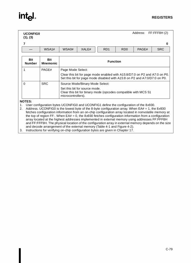
REGISTERS
1 PAGE# Page Mode Select:
Clear this bit for page mode enabled with A15:8/D7:0 on P2 and A7:0 on P0.Set this bit for page mode disabled with A15:8 on P2 and A7:0/D7:0 on P0.
0 SRC Source Mode/Binary Mode Select:
Set this bit for source mode.Clear this bit for binary mode (opcodes compatible with MCS 51 microcontrollers).
UCONFIG0(1), (3)
Address: FF:FFF8H (2)
7 0
— WSA1# WSA0# XALE# RD1 RD0 PAGE# SRC
Bit Number
Bit Mnemonic Function
NOTES:1. User configuration bytes UCONFIG0 and UCONFIG1 define the configuration of the 8x930.2. Address. UCONFIG0 is the lowest byte of the 8-byte configuration array. When EA# = 1, the 8x930
fetches configuration information from an on-chip configuration array located in nonvolatile memory at the top of region FF:. When EA# = 0, the 8x930 fetches configuration information from a configuration array located at the highest addresses implemented in external memory using addresses FF:FFF8H and FF:FFF9H. The physical location of the configuration array in external memory depends on the size and decode arrangement of the external memory (Table 4-1 and Figure 4-2).
3. Instructions for verifying on-chip configuration bytes are given in Chapter 17.
C-79

8x930Ax, 8x930Hx USER’S MANUAL
UCONFIG1 (1),(3)
Address: FF:FFF9H (2)
7 0
— — — INTR — WSB1# WSB0# EMAP#
Bit Number
Bit Mnemonic Function
7:5 — Reserved:
Reserved for internal or future use. Set these bits when programming UCONFIG1.
4 INTR Interrupt Mode:
If this bit is set, interrupts push 4 bytes onto the stack (the 3 bytes of the PC and PSW1). If this bit is clear, interrupts push the 2 lower bytes of the PC onto the stack. See “Interrupt Mode (INTR)” on page 4-14.
3 — Reserved. Write a ‘1’ to this bit.
2:1 WSB1:0#
External Wait State B (Region 01:):
WSB1# WSB0#0 0 Inserts 3 wait states for region 01: 0 1 Inserts 2 wait states for region 01: 1 0 Inserts 1 wait state for region 01: 1 1 Zero wait states for region 01:
0 EMAP# EPROM Map:
For devices with 16 Kbytes of on-chip code memory, clear this bit to map the upper half of on-chip code memory to region 00: (data memory). This maps FF:2000H–FF:3FFFH to 00:E000H–00:FFFFH. If this bit is set, mapping does not occur and addresses in the range 00:E000H–00:FFFFH access external RAM. See “Mapping On-chip Code Memory to Data Memory (EMAP#)” on page 14.
NOTES:1. User configuration bytes UCONFIG0 and UCONFIG1 define the configuration of the 8x930.2. Address. UCONFIG1 is the second lowest byte of the 8-byte configuration array. When EA# = 1, the
8x930 fetches configuration information from an on-chip configuration array located in nonvolatile memory at the top of region FF:. When EA# = 0, the 8x930 fetches configuration information from a configuration array located at the highest addresses implemented in external memory using addresses FF:FFF8H and FF:FFF9H. The physical location of the configuration array in external memory depends on the size and decode arrangement of the external memory (Table 4-1 and Figure 4-2).
3. Instructions for verifying on-chip configuration bytes are given in Chapter 17.
C-80

DData Flow Model

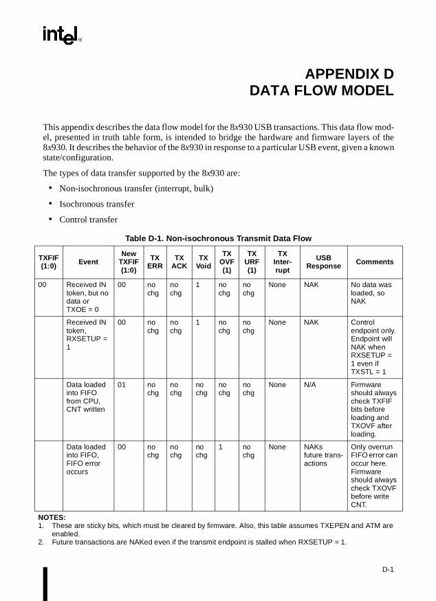
of thewn
APPENDIX DDATA FLOW MODEL
This appendix describes the data flow model for the 8x930 USB transactions. This data flow mod-el, presented in truth table form, is intended to bridge the hardware and firmware layers 8x930. It describes the behavior of the 8x930 in response to a particular USB event, given a knostate/configuration.
The types of data transfer supported by the 8x930 are:
• Non-isochronous transfer (interrupt, bulk)
• Isochronous transfer
• Control transfer
Table D-1. Non-isochronous Transmit Data Flow
TXFIF(1:0) Event
New TXFIF(1:0)
TXERR
TXACK
TXVoid
TX OVF(1)
TX URF(1)
TXInter-rupt
USB Response Comments
00 Received IN token, but no data or TXOE = 0
00 no chg
no chg
1 no chg
no chg
None NAK No data was loaded, so NAK
Received IN token, RXSETUP = 1
00 no chg
no chg
1 no chg
no chg
None NAK Control endpoint only. Endpoint will NAK when RXSETUP = 1 even if TXSTL = 1
Data loaded into FIFO from CPU, CNT written
01 no chg
no chg
no chg
no chg
no chg
None N/A Firmware should always check TXFIF bits before loading and TXOVF after loading.
Data loaded into FIFO, FIFO error occurs
00 no chg
no chg
no chg
1 no chg
None NAKs future trans-actions
Only overrun FIFO error can occur here. Firmware should always check TXOVF before write CNT.
NOTES:1. These are sticky bits, which must be cleared by firmware. Also, this table assumes TXEPEN and ATM are
enabled.2. Future transactions are NAKed even if the transmit endpoint is stalled when RXSETUP = 1.
D-1

8x930Ax, 8x930Hx USER’S MANUAL
01/10 Received IN token, data transmitted, host ACKs
00 0 1 0 no chg
no chg
Set transmit interrupt
Send data ACK received, so no errors. Read marker advanced
Received IN token, data transmitted, no ACK (time-out)
01/10 1 0 0 no chg
no chg
Set transmit interrupt
Send data SIE times-out. Read ptr reversed.
Received IN token, but RXSETUP = 1 (or TXOE = 0)
01/10 no chg
no chg
1 no chg
no chg
None NAK, NAKs future trans-actions except SETUP.
Received Setup token (or transmit disabled), so IN tokens are NAKed. (2)
Received IN token, data transmitted, FIFO error occurs
01/10 1 0 0 no chg
1 Set transmit interrupt
Send data with bit-stuff error. NAKs future trans-actions.
Only underrun FIFO error can occur here. Read ptr reversed.
Received IN token with existing FIFO error and TXERR set.
01/10 1 (no chg)
0 (no chg)
1 no chg
1 (no chg)
None NAK Treated like a “void” condition.
Received IN token without existing FIFO error but TXERR set, data retrans-mitted, host ACKs
00 0 1 0 no chg
no chg
Set transmit interrupt
Send data Data is retransmitted. TXACK is set and TXERR is cleared. The TXERR was set by previous transaction when host time-out.
Table D-1. Non-isochronous Transmit Data Flow (Continued)
TXFIF(1:0) Event
New TXFIF(1:0)
TXERR
TXACK
TXVoid
TX OVF(1)
TX URF(1)
TXInter-rupt
USB Response Comments
NOTES:1. These are sticky bits, which must be cleared by firmware. Also, this table assumes TXEPEN and ATM are
enabled.2. Future transactions are NAKed even if the transmit endpoint is stalled when RXSETUP = 1.
D-2

DATA FLOW MODEL
Data loaded into FIFO from CPU, CNT written
11 no chg
no chg
no chg
no chg
no chg
None N/A Firmware should always check TXFIF bits before loading and TXOVF after loading.
Data loaded into FIFO, FIFO error occurs. CNT not written yet.
01/10 no chg
no chg
no chg
1 no chg
None NAKs futuretransactions
Only overrun FIFO error can occur here. Firmware should always check TXOVF before write CNT
NOTE: no TXERR, but TXOVF set.
11 Received IN token, data transmitted, host ACKs
10/01 0 1 0 no chg
no chg
Set transmit interrupt
Send data ACK received, so no errors. Read marker advanced.
Received IN token, data transmitted, no ACK (time-out)
11 1 0 0 no chg
no chg
Set transmit interrupt
Send data SIE times-out. Read ptr reversed.
Received IN token, but RXSETUP = 1 (or TXOE = 0)
11 0 0 1 no chg
no chg
None NAK, NAKs future trans-actions
Received Setup token (or transmit disabled), so IN tokens are NAKed. (2)
Received IN token, data transmitted, FIFO error occurs
11 1 0 0 no chg
1 Set transmit interrupt
Send data with bit-stuff error, NAK future transactions
Only FIFO underrun error can occur here. Read ptr reversed.
Table D-1. Non-isochronous Transmit Data Flow (Continued)
TXFIF(1:0) Event
New TXFIF(1:0)
TXERR
TXACK
TXVoid
TX OVF(1)
TX URF(1)
TXInter-rupt
USB Response Comments
NOTES:1. These are sticky bits, which must be cleared by firmware. Also, this table assumes TXEPEN and ATM are
enabled.2. Future transactions are NAKed even if the transmit endpoint is stalled when RXSETUP = 1.
D-3

8x930Ax, 8x930Hx USER’S MANUAL
Received IN token with existing FIFO error and TXERR set.
11 1 (no chg)
0 (no chg)
1 no chg
1 (no chg)
None NAK Treated like a “void” condition.
Received IN token without existing FIFO error but TXERR set, data retrans-mitted, host ACKs
10/ 01 0 1 0 no chg
no chg
Set transmit interrupt
Send data Data is retransmitted. TXACK is set and TXERR is cleared. The TXERR was set by previous transaction when host time-out.
Data loaded into FIFO from CPU, CNT written
11 no chg
no chg
no chg
1 no chg
None N/A Writing into CNT when TXFIF = 11 sets TXOVF bit. Firmware should always check TXFIF bits before loading.
Table D-1. Non-isochronous Transmit Data Flow (Continued)
TXFIF(1:0) Event
New TXFIF(1:0)
TXERR
TXACK
TXVoid
TX OVF(1)
TX URF(1)
TXInter-rupt
USB Response Comments
NOTES:1. These are sticky bits, which must be cleared by firmware. Also, this table assumes TXEPEN and ATM are
enabled.2. Future transactions are NAKed even if the transmit endpoint is stalled when RXSETUP = 1.
D-4

DATA FLOW MODEL
T(
0
0
N12
3
Table D-2. Isochronous Transmit Data Flow in Dual-packet Mode
XFIF1:0) Event
New TXFIF
(1:0)(2)
(at next SOF)TX
OVF(1,2)
TX URF(1,2)
TXInter-rupt
USB Response CommentsTX
ERR TX
ACK TX
Void
0 Received IN token, but no data or TXOE=0
00 no chg
no chg
1 no chg
no chg
None Send null data packet
No data was loaded, so sendnull data packet. This event should never happen.
Data loaded into FIFO from CPU, CNT written
01 no chg
no chg
no chg
no chg
no chg
None N/A Firmware should always check TXFIF bits before loading and TXOVF after loading.
Data loaded into FIFO, FIFO error
00 no chg
no chg
no chg
1 no chg
None N/A Only overrun FIFO error canoccur here. Firmware should always check TXOVF before write CNT
1/10 Received IN token, data transmitted with or without trans-mission error
00 0 1 0 no chg
no chg
None Send data No ACK (time-out) for ISO. Read marker advanced.
Received IN token, data transmitted, FIFO error occurs
00 1 0 0 no chg
1 None Send CRC with bit-stuff error
Only underrun FIFO error canoccur here. Read marker advanced.
OTES:. These are sticky bits, which must be cleared by firmware.. TXFIF, TXOVF and TXURF are handled with the following golden rule: Firmware events cause status change
immediately while USB events only cause status change at SOF.TXOVF: Since overrun can only be caused by firmware, TXOVF is updated immediately.TXURF: Since underrun can only be caused by USB, TXURF is updated at SOF.TXFIF: TXFIF is “incremented” by firmware and “decremented” by USB. Therefore, writes to TXCNT will “increment” TXFIF immediately. However, a successful USB transaction anytime in a frame will only “decrement”TXFIF at SOF.TXERR, TXACK, and TXVOID can only be caused by USB; thus they are updated at the end of every valid transaction.
. NOTE: This table assumes TXEPEN and ATM are enabled.
D-5

8x930Ax, 8x930Hx USER’S MANUAL
.
11
T(
N12
3
Received IN token with existing FIFO error
01/10 1 (no chg)
0 (no chg)
1 no chg
1 (no chg)
None Send null data packet
Treated like a “void” condition
Received IN token, but TXOE = 0
01/10 0 0 1 no chg
no chg
None Send null data packet
Endpoint not enabled for transmit, but no NAK for ISO.
Data loaded into FIFO from CPU, CNT written
11 no chg
no chg
no chg
no chg
no chg
None N/A Firmware should always check TXFIF bits before loading and TXOVF after loading.
Data loaded into FIFO, FIFO error occurs
01/10 no chg
no chg
no chg
1 no chg
None N/A Only overrun FIFO error canoccur here. Firmware should always check TXOVF before write CNT
Note: no TXERR, but TXOVF set.
Received IN token, data transmitted with or without trans-mission error
10/01 0 1 0 no chg
no chg
None Send data No ACK (time-out) for ISO. Read marker advanced.
Table D-2. Isochronous Transmit Data Flow in Dual-packet Mode (Continued)
XFIF1:0) Event
New TXFIF
(1:0)(2)
(at next SOF)TX
OVF(1,2)
TX URF(1,2)
TXInter-rupt
USB Response CommentsTX
ERR TX
ACK TX
Void
OTES:. These are sticky bits, which must be cleared by firmware.. TXFIF, TXOVF and TXURF are handled with the following golden rule: Firmware events cause status change
immediately while USB events only cause status change at SOF.TXOVF: Since overrun can only be caused by firmware, TXOVF is updated immediately.TXURF: Since underrun can only be caused by USB, TXURF is updated at SOF.TXFIF: TXFIF is “incremented” by firmware and “decremented” by USB. Therefore, writes to TXCNT will “increment” TXFIF immediately. However, a successful USB transaction anytime in a frame will only “decrement”TXFIF at SOF.TXERR, TXACK, and TXVOID can only be caused by USB; thus they are updated at the end of every valid transaction.
. NOTE: This table assumes TXEPEN and ATM are enabled.
D-6

DATA FLOW MODEL
.
T(
N12
3
Received IN token, data transmitted, FIFO error occurs
10/01 1 0 0 no chg
1 None Send data with bitstuff error
Only a FIFO underrun error can occur here. Read marker advanced.
Received IN token with existing FIFO error
11 1 (no chg)
0 (no chg)
1 no chg
1 (no chg)
None Send null data packet
Treated like a “void” condition
Received IN token, but TXOE = 0
11 0 0 1 no chg
no chg
None Send null data packet
Endpoint not enabled for transmit, but no NAK for ISO.
Receive SOF indication
10/01 no chg
no chg
no chg
no chg
no chg
None (SOF interrupt set)
ASOF set.
None Host never readlast frame’s ISO. packet. Read marker and ptr advanced, oldest packet is flushed from FIFO.
Data loaded into FIFO from CPU, CNT written
11 no chg
no chg
no chg
1 no chg
None N/A CNT written when TXFIF=11 will set TXOVF bit.
Firmware should always check TXFIF bits before loading.
Table D-2. Isochronous Transmit Data Flow in Dual-packet Mode (Continued)
XFIF1:0) Event
New TXFIF
(1:0)(2)
(at next SOF)TX
OVF(1,2)
TX URF(1,2)
TXInter-rupt
USB Response CommentsTX
ERR TX
ACK TX
Void
OTES:. These are sticky bits, which must be cleared by firmware.. TXFIF, TXOVF and TXURF are handled with the following golden rule: Firmware events cause status change
immediately while USB events only cause status change at SOF.TXOVF: Since overrun can only be caused by firmware, TXOVF is updated immediately.TXURF: Since underrun can only be caused by USB, TXURF is updated at SOF.TXFIF: TXFIF is “incremented” by firmware and “decremented” by USB. Therefore, writes to TXCNT will “increment” TXFIF immediately. However, a successful USB transaction anytime in a frame will only “decrement”TXFIF at SOF.TXERR, TXACK, and TXVOID can only be caused by USB; thus they are updated at the end of every valid transaction.
. NOTE: This table assumes TXEPEN and ATM are enabled.
D-7

8x930Ax, 8x930Hx USER’S MANUAL
F(1
0
)
.
N1
2
Table D-3. Non-isochr onous Receive Data Flow in Single-packet Mode (RXSPM = 1)
IF:0) Event
New FIF(1:0)
RXERR
RXACK
RXVoid
RXSetup
RX OVF(1)
RX URF(1)
RXInter-rupt
USB Response Comments
0 Received OUT token, but RXIE = 0
00 no chg
no chg
1 no chg
no chg
no chg
None NAK FIFO not ready.
Received OUT token, but timed-out waiting for data
00 no chg
no chg
no chg
no chg
no chg
no chg
None None FIFO not loaded. Write ptr reversed.
Received OUT token, no errors
01 0 1 0 0 no chg
no chg
Set receive interrupt
ACK Received, no errors, advancewrite marker.
Received OUT token, data CRC or bit-stuff error
00 1 0 0 0 no chg
no chg
Set receive interrupt
Time-out Write ptr reversed. (Possible to have RXERR cleared by hardware before seen by firmware.)
Received OUT token, FIFO error occurs
00 1 0 0 0 1 no chg
Set receive interrupt
Time-out, NAK future transac-tions
Only RXOVF FIFO error can occur, requires firmware inter-vention.
Received OUT token with FIFO error already existing
00 1 (no chg)
0 (no chg)
1 0 1 (no chg)
no chg
None NAK Considered to be a “void” condition. Will NAK until firmware clearscondition.
Received OUT token, but data sequence mismatch
00 no chg
no chg
1 no chg
no chg
no chg
None ACK Last ACK corrupted, so send again but ignore the data.
Received SETUP token, no errors
01 0 1 0 1 0 0 Set receive interrupt
ACK RXIE or RXSTLhas no effect.(2RXSETUP will be set (control endpoints only)
OTE:. These are sticky bits, which must be cleared by firmware. Also, this table assumes RXEPEN and ARM are
enabled.. STOVW is set after a valid SETUP token is received and cleared during handshake phase. EDOVW is set during
handshake phase.
D-8

DATA FLOW MODEL
.
0
T
F(1
N1
2
Received SETUP token, but timed-out waiting for data
00 1 0 0 0 0 0 Set receive interrupt
Time-out FIFO is reset automatically and FIFO data is invalid. (2)
Received SETUP token, data CRC or bit-stuff error
00 1 0 0 1 0 0 Set receive interrupt
Time-out Write ptr reversed, (2)
Received SETUP token, FIFO error occurs
00 1 0 0 1 1 0 Set receive interrupt
Time-out, NAK future transac-tions
(2)
Received SETUP token with FIFO error already existing
01 0 1 0 1 0 0 Set receive interrupt
ACK Causes FIFO to reset automatically, forcing new SETUP to be received.RXIE or RXSTL has no effect. (2) RXSETUP will be set (control endpoints only)
CPU reads FIFO, causes FIFO error
00 no chg
no chg
no chg
no chg
no chg
1 None NAK future transac-tions, except SETUP
FIFO was empty when read. Should always check RXFIF bits before reading.
1 Received OUT token
01 no chg
no chg
1 no chg
no chg
no chg
None NAK FIFO not ready,so data is ignored (CRC orFIFO error not possible)
able D-3. Non-isochronous Receive Data Flow in Single-packet Mode (RXSPM = 1) (Continued)
IF:0) Event
New FIF(1:0)
RXERR
RXACK
RXVoid
RXSetup
RX OVF(1)
RX URF(1)
RXInter-rupt
USB Response Comments
OTE:. These are sticky bits, which must be cleared by firmware. Also, this table assumes RXEPEN and ARM are
enabled.. STOVW is set after a valid SETUP token is received and cleared during handshake phase. EDOVW is set during
handshake phase.
D-9

8x930Ax, 8x930Hx USER’S MANUAL
.
.
.
.
T
F(1
N1
2
Received SETUP token, no errors
01 0 1 0 1 0 0 Set receive interrupt
ACK Causes FIFO to reset automatically, forcing new SETUP to be received. RXIE or RXSTL has no effect. (2) RXSETUP will be set (control endpoints only)
Received SETUP token, but timed-out waiting for data
01 1 0 0 0 0 0 Set receive interrupt
Time-out FIFO is reset automatically and FIFO data is invalid. (2)
Received SETUP token, data CRC or bit-stuff error
00 1 0 0 1 0 0 Set receive interrupt
Time-out Write ptr reversed. RXIEor RXSTL has no effect. (2) RXSETUP will be set (control endpoints only)
Received SETUP token, FIFO error occurs
00 1 0 0 1 1 0 Set receive interrupt
Time-out, NAK future transac-tions
(2) (control endpoints only)
Received SETUP token with FIFO error already existing
01 0 1 0 1 0 0 Set receive interrupt
ACK Causes FIFO to reset automatically, forcing new SETUP to be received. RXIE or RXSTL has no effect. (2) RXSETUP will be set (control endpoints only)
CPU reads FIFO, sets RXFFRC
00 no chg
no chg
no chg
no chg
no chg
no chg
None None
able D-3. Non-isochronous Receive Data Flow in Single-packet Mode (RXSPM = 1) (Continued)
IF:0) Event
New FIF(1:0)
RXERR
RXACK
RXVoid
RXSetup
RX OVF(1)
RX URF(1)
RXInter-rupt
USB Response Comments
OTE:. These are sticky bits, which must be cleared by firmware. Also, this table assumes RXEPEN and ARM are
enabled.. STOVW is set after a valid SETUP token is received and cleared during handshake phase. EDOVW is set during
handshake phase.
D-10

DATA FLOW MODEL
FI(1:
00
.
NO1. d.2.
3.
T
F(1
N1
2
CPU reads FIFO, causes FIFO error. RXFFRC not set yet.
01 no chg
no chg
no chg
no chg
no chg
1 None Time-out, NAK future transac-tions
Firmware should check RXURF bit before writing RXFFRC.
CPU reads FIFO, causes FIFO error. Set RXFFRC.
00 no chg
no chg
no chg
no chg
no chg
1 None Time-out, NAK future transac-tions
Firmware should check RXURF bit before writing RXFFRC.
Table D-4. Non-isochronous Receive Data Flow in Dual-packet Mode (RXSPM = 0)
F0) Event
New FIF
(1:0)
RXERR
RXACK
RXVoid
RXSetup
RXOVF(1)
RXURF(1)
RXInter-rupt
USB Response Comments
Received OUT token, but RXIE = 0
00 no chg
no chg
1 no chg
no chg
no chg
None NAK FIFO not ready.
Received OUT token, but timed-out waiting for data
00 no chg
no chg
1 no chg
no chg
no chg
None None FIFO not loadedWrite ptr reversed.
Received OUT token, no errors
01 0 1 0 0 no chg
no chg
Set receive interrupt
ACK Received, no errors, advancewrite marker.
TES:These are sticky bits, which must be cleared by firmware. Also, this table assumes RXEPEN and ARM are enableSTOVW is set after a valid SETUP token is received and cleared during handshake phase. EDOVW is set duringhandshake phase.NOTE: Dual-packet mode is NOT recommended for control endpoints.
able D-3. Non-isochronous Receive Data Flow in Single-packet Mode (RXSPM = 1) (Continued)
IF:0) Event
New FIF(1:0)
RXERR
RXACK
RXVoid
RXSetup
RX OVF(1)
RX URF(1)
RXInter-rupt
USB Response Comments
OTE:. These are sticky bits, which must be cleared by firmware. Also, this table assumes RXEPEN and ARM are
enabled.. STOVW is set after a valid SETUP token is received and cleared during handshake phase. EDOVW is set during
handshake phase.
D-11

8x930Ax, 8x930Hx USER’S MANUAL
e
e
w
o
e
.
d
FI(1:
NO1. d.2.
3.
Received OUT token, data CRC or bit-stuff error
00 1 0 0 0 no chg
no chg
Set receive interrupt
Time-out Write ptr reversed. (Possible to havRXERR clearedby hardware before seen by firmware.)
Received OUT token, FIFO error occurs
00 1 0 0 0 1 no chg
Set receive interrupt
Time-out, NAK future transac-tions
Only RXOVF FIFO error can occur, requires firmware inter-vention.
Received OUT token with FIFO error already existing
00 1 (no chg)
0 (no chg)
1 0 1 (no chg)
no chg
None NAK Considered to ba “void” condition. Will NAK until firmware clearscondition.
Received OUT token, but data sequence mismatch
00 no chg
no chg
no chg
no chg
no chg
no chg
None ACK Last ACK corrupted, so send again but ignore the data.
Received SETUP token, no errors (dual packet mode not recom-mended!)
01 0 1 0 1 0 0 Set receive interrupt
ACK Causes FIFO toreset automati-cally, forcing neSETUP to be received. RXIE or RXSTL has neffect. (2) RXSETUP will bset (control endpoints only)
Received SETUP token, but timed-out waiting for data
00 1 0 0 0 0 0 Set receive interrupt
Time-out FIFO is reset automatically anFIFO data is invalid. (2)
Table D-4. Non-isochronous Receive Data Flow in Dual-packet Mode (RXSPM = 0) (Continued)
F0) Event
New FIF
(1:0)
RXERR
RXACK
RXVoid
RXSetup
RXOVF(1)
RXURF(1)
RXInter-rupt
USB Response Comments
TES:These are sticky bits, which must be cleared by firmware. Also, this table assumes RXEPEN and ARM are enableSTOVW is set after a valid SETUP token is received and cleared during handshake phase. EDOVW is set duringhandshake phase.NOTE: Dual-packet mode is NOT recommended for control endpoints.
D-12

DATA FLOW MODEL
o
e
.
) e
.
w
o
e
.
y
ts
01/
.
FI(1:
NO1. d.2.
3.
Received SETUP token, data CRC or bit-stuff error (dual packet mode not recom-mended)
00 1 0 0 1 0 0 Set receive interrupt
Time-out Write ptr reversed, RXIEor RXSTL has neffect. (2) RXSETUP will bset (control endpoints only)
Received SETUP token, FIFO error occurs
00 1 0 0 1 1 0 Set receive interrupt
Time-out, NAK future transac-tions
RXIE or RXSTLhas no effect. (2RXSETUP will bset (control endpoints only)
Received SETUP token with FIFO error already existing
01 0 1 0 1 0 0 Set receive interrupt
ACK Causes FIFO toreset automati-cally, forcing neSETUP to be received. RXIE or RXSTL has neffect. (2) RXSETUP will bset (control endpoints only)
CPU reads FIFO, causes FIFO error
00 no chg
no chg
no chg
no chg
no chg
1 None NAK future transac-tions
FIFO was emptwhen read. Should always check RXFIF bibefore reading.
10 Received OUT token, but RXIE = 0
01/10 no chg
no chg
1 no chg
no chg
no chg
None NAK FIFO not ready.
Received OUT token, but timed-out waiting for data
01/10 no chg
no chg
1 no chg
no chg
no chg
None None FIFO not loadedWrite ptr reversed.
Received OUT token, no errors
11 0 1 0 0 no chg
no chg
Set receive interrupt
ACK Received, no errors, advancewrite marker.
Table D-4. Non-isochronous Receive Data Flow in Dual-packet Mode (RXSPM = 0) (Continued)
F0) Event
New FIF
(1:0)
RXERR
RXACK
RXVoid
RXSetup
RXOVF(1)
RXURF(1)
RXInter-rupt
USB Response Comments
TES:These are sticky bits, which must be cleared by firmware. Also, this table assumes RXEPEN and ARM are enableSTOVW is set after a valid SETUP token is received and cleared during handshake phase. EDOVW is set duringhandshake phase.NOTE: Dual-packet mode is NOT recommended for control endpoints.
D-13

8x930Ax, 8x930Hx USER’S MANUAL
e
e
w
o
e
.
FI(1:
NO1. d.2.
3.
Received OUT token, data CRC or bit-stuff error
01/10 1 0 0 0 no chg
no chg
Set receive interrupt
Time-out Write ptr reversed. (Possible to havRXERR clearedby hardware before seen by firmware.)
Received OUT token, FIFO error occurs
01/10 1 0 0 0 1 no chg
Set receive interrupt
Time-out, NAK future transac-tions
Only RXOVF FIFO error can occur, requires firmware inter-vention.
Received OUT token with FIFO error already existing
01/10 1 (no chg)
0 (no chg)
1 0 1 (no chg)
no chg
None NAK Considered to ba “void” condition. Will NAK until firmware clearscondition.
Received OUT token, but data sequence mismatch
01/10 no chg
no chg
no chg
no chg
no chg
no chg
None ACK Last ACK corrupted, so send again but ignore the data.
Received SETUP token, no errors (dual-packet mode not recom-mended)
01/10 0 1 0 1 0 0 Set receive interrupt
ACK Causes FIFO toreset automati-cally, forcing neSETUP to be received. RXIE or RXSTL has neffect. (2) RXSETUP will bset (control endpoints only)
Received SETUP token, but timed-out waiting for data
01/10 1 0 0 0 0 0 Set receive interrupt
Time-out FIFO is reset automatically, forcing new SETUP to be received. (2)
Table D-4. Non-isochronous Receive Data Flow in Dual-packet Mode (RXSPM = 0) (Continued)
F0) Event
New FIF
(1:0)
RXERR
RXACK
RXVoid
RXSetup
RXOVF(1)
RXURF(1)
RXInter-rupt
USB Response Comments
TES:These are sticky bits, which must be cleared by firmware. Also, this table assumes RXEPEN and ARM are enableSTOVW is set after a valid SETUP token is received and cleared during handshake phase. EDOVW is set duringhandshake phase.NOTE: Dual-packet mode is NOT recommended for control endpoints.
D-14

DATA FLOW MODEL
o
) e
.
w
e
.
d it
d it
11
r
FI(1:
NO1. d.2.
3.
Received SETUP token, data CRC or bit-stuff error (dual-packet mode not recom-mended)
00 1 0 0 1 0 0 Set receive interrupt
Time-out Write ptr reversed. RXIEor RXSTL has neffect. (2)
Received SETUP token, FIFO error occurs
00 1 0 0 1 1 0 Set receive interrupt
Time-out, NAK future transac-tions
RXIE or RXSTLhas no effect, (2RXSETUP will bset (control endpoints only)
Received SETUP token with FIFO error already existing
01/10 0 1 0 1 0 0 Set receive interrupt
ACK Causes FIFO toreset automati-cally, forcing neSETUP to be received. (2) RXSETUP will bset (control endpoints only)
CPU reads FIFO, sets RXFFRC
00 no chg
no chg
no chg
no chg
no chg
no chg
None None
CPU reads FIFO, causes FIFO error. RXFFRC not set yet.
01/10 no chg
no chg
no chg
no chg
no chg
1 None Time-out, NAK future transac-tions
Firmware shoulcheck RXURF bbefore writing RXFFRC.
CPU reads FIFO, causes FIFO error. Set RXFFRC.
00 no chg
no chg
no chg
no chg
no chg
1 None Time-out, NAK future transac-tions
Firmware shoulcheck RXURF bbefore writing RXFFRC.
Received OUT token
11 no chg
no chg
1 no chg
no chg
no chg
None NAK FIFO not ready,so data is ignored (CRC oFIFO error not possible).
Table D-4. Non-isochronous Receive Data Flow in Dual-packet Mode (RXSPM = 0) (Continued)
F0) Event
New FIF
(1:0)
RXERR
RXACK
RXVoid
RXSetup
RXOVF(1)
RXURF(1)
RXInter-rupt
USB Response Comments
TES:These are sticky bits, which must be cleared by firmware. Also, this table assumes RXEPEN and ARM are enableSTOVW is set after a valid SETUP token is received and cleared during handshake phase. EDOVW is set duringhandshake phase.NOTE: Dual-packet mode is NOT recommended for control endpoints.
D-15

8x930Ax, 8x930Hx USER’S MANUAL
w
e
.
d
o
) e
.
w
e
.
FI(1:
NO1. d.2.
3.
Received SETUP token, no errors (dual-packet mode not recom-mended!)
01 0 1 0 1 0 0 Set receive interrupt
ACK Causes FIFO toreset automati-cally, forcing neSETUP to be received. (2) RXSETUP will bset. (control endpoints only)
Received SETUP token, but timed-out waiting for data
11 1 0 0 0 0 0 Set receive interrupt
Time-out FIFO is reset automatically anFIFO data is invalid. (2)
Received SETUP token, data CRC or bit-stuff error (dual-packet mode not recom-mended).
00 1 0 0 1 0 0 Set receive interrupt
Time-out Write ptr reversed. RXIEor RXSTL has neffect. (2)
Received SETUP token, FIFO error (dual-packet mode not recom-mended).
00 1 0 0 1 1 0 Set receive interrupt
Time-out, NAK future transac-tions
RXIE or RXSTLhas no effect. (2RXSETUP will bset (control endpoints only)
Received SETUP token with FIFO error already existing
01 0 1 0 1 0 0 Set receive interrupt
ACK Causes FIFO toreset automati-cally, forcing neSETUP to be received. (2) RXSETUP will bset (control endpoints only)
CPU reads FIFO, sets RXFFRC
10/01 no chg
no chg
no chg
no chg
no chg
no chg
None None
Table D-4. Non-isochronous Receive Data Flow in Dual-packet Mode (RXSPM = 0) (Continued)
F0) Event
New FIF
(1:0)
RXERR
RXACK
RXVoid
RXSetup
RXOVF(1)
RXURF(1)
RXInter-rupt
USB Response Comments
TES:These are sticky bits, which must be cleared by firmware. Also, this table assumes RXEPEN and ARM are enableSTOVW is set after a valid SETUP token is received and cleared during handshake phase. EDOVW is set duringhandshake phase.NOTE: Dual-packet mode is NOT recommended for control endpoints.
D-16

DATA FLOW MODEL
d it
d it
FI(1:
NO1. d.2.
3.
CPU reads FIFO, causes FIFO error. RXFFRC not written yet.
11 no chg
no chg
no chg
no chg
no chg
1 None NAKs future transac-tions
Firmware shoulcheck RXURF bbefore writing FFRC
CPU reads FIFO, causes FIFO error. Set RXFFRC.
10/01 no chg
no chg
no chg
no chg
no chg
1 None NAKs future transac-tions
Firmware shoulcheck RXURF bbefore writing FFRC
Table D-4. Non-isochronous Receive Data Flow in Dual-packet Mode (RXSPM = 0) (Continued)
F0) Event
New FIF
(1:0)
RXERR
RXACK
RXVoid
RXSetup
RXOVF(1)
RXURF(1)
RXInter-rupt
USB Response Comments
TES:These are sticky bits, which must be cleared by firmware. Also, this table assumes RXEPEN and ARM are enableSTOVW is set after a valid SETUP token is received and cleared during handshake phase. EDOVW is set duringhandshake phase.NOTE: Dual-packet mode is NOT recommended for control endpoints.
D-17

8x930Ax, 8x930Hx USER’S MANUAL
FI(1:
00 y,
a
d.
e
n.
.
NO1. d.2.
Table D-5. Isochronous Receive Data Flow in Dual-packet Mode (RXSPM = 0)
F0) Event
New RXFIF(1:0)(2)
(at next SOF) RX OVF(1,2)
RX URF(1,2)
RX Inter-rupt
USB Response CommentsRX
ERRRX
ACKRX
Void
Received OUT token, but RXIE = 0
00 no chg
no chg
1 no chg
no chg
None None/Time-out
FIFO not reador timed-out waiting for datpacket, but noNAK sent
Received OUT token, but timed-out waiting for data
00 no chg
no chg
no chg
no chg
no chg
None None/Time-out
FIFO not loade
Received OUT token, no errors
01 0 1 0 no chg
no chg
None None/Time-out
Received, no errors, advancwrite marker
Received OUT token, data CRC or bit-stuff error
01 1 0 0 no chg
no chg
None None/Time-out
Bad data still loaded into FIFO.
Received OUT token, FIFO error occurs
01 1 0 0 1 no chg
None None/Time-out
Only RXOVF FIFO error canoccur, requiresfirmware inter-vention.
Received OUT token with FIFO error already existing
00 1(no chg)
0 (no chg)
1 1 (no chg)
no chg
None None/Time-out
Treated like a “void” conditio
CPU reads FIFO, causes FIFO error
00 no chg
no chg
no chg
no chg
1 None None/Time-out
FIFO was empty when read. Should always check RXFIF bits before reading
TES:These are sticky bits, which must be cleared by firmware. Also, this table assumes RXEPEN and ARM are enableRXFIF, RXOVF and RXURF are handled with the following golden rule: Firmware events cause status change immediately while USB events only cause status change at SOF.RXURF: Since underrun can only be caused by firmware, RXURF is updated immediately.RXOVF: Since overrun can only be caused by USB, RXOVF is updated at SOF.RXFIF: RXFIF is “incremented” by USB and “decremented” by firmware. Therefore, setting RXFFRC will “decrement” RXFIF immediately. However, a successful USB transaction anytime in a frame will only “increment” RXFIF at SOF.RXERR, RXACK, and RXVOID can only be caused by USB, thus they are updated at the end of transaction.
D-18

DATA FLOW MODEL
d
01/ y.
d.
e
r,
n.
FI(1:
NO1. d.2.
Receive SOF indication
no chg/updated
up-dated
up-dated
up-dated
up-dated
no chg
None (SOF interrupt)
None/Time-out
Flags are updated at SOF. Firmwaremust check forRXFIF = 00 condition to detect no ISO packet receivethis frame.
10 Received OUT token, but RXIE = 0
01/10 no chg
no chg
1 no chg
no chg
None None/Time-out
FIFO not read
Received OUT token, but timed-out waiting for data
01/10 no chg
no chg
no chg
no chg
no chg
None None/Time-out
FIFO not loade
Received OUT token, no errors
11 0 1 0 no chg
no chg
None None/Time-out
Received, no errors, advancwrite marker.
Received OUT token, data CRC or bit-stuff error
11 1 0 0 no chg
no chg
None None/Time-out
Possible to have RXERR cleared by hardware before seen byfirmware. Reverse write pointer.
Received OUT token, FIFO error occurs
11 1 0 0 1 no chg
None None/Time-out
Only OVF FIFOerror can occurequires firmware inter-vention.
Received OUT token with FIFO error already existing
01/10 no chg
no chg
1 no chg
no chg
None None/Time-out
Treated like a “void” conditio
Table D-5. Isochronous Receive Data Flow in Dual-packet Mode (RXSPM = 0) (Continued)
F0) Event
New RXFIF(1:0)(2)
(at next SOF) RX OVF(1,2)
RX URF(1,2)
RX Inter-rupt
USB Response CommentsRX
ERRRX
ACKRX
Void
TES:These are sticky bits, which must be cleared by firmware. Also, this table assumes RXEPEN and ARM are enableRXFIF, RXOVF and RXURF are handled with the following golden rule: Firmware events cause status change immediately while USB events only cause status change at SOF.RXURF: Since underrun can only be caused by firmware, RXURF is updated immediately.RXOVF: Since overrun can only be caused by USB, RXOVF is updated at SOF.RXFIF: RXFIF is “incremented” by USB and “decremented” by firmware. Therefore, setting RXFFRC will “decrement” RXFIF immediately. However, a successful USB transaction anytime in a frame will only “increment” RXFIF at SOF.RXERR, RXACK, and RXVOID can only be caused by USB, thus they are updated at the end of transaction.
D-19

8x930Ax, 8x930Hx USER’S MANUAL
11 y, e
d
y
w
FI(1:
NO1. d.2.
CPU reads FIFO, sets RXFFRC
00 no chg
no chg
no chg
no chg
no chg
None None/Time-out
CPU reads FIFO, causes FIFO error
00 no chg
no chg
no chg
no chg
1 None None/Time-out
Firmware should check RXURF bit before writing RXFFRC.
Received OUT token
11 no chg
no chg
1 no chg
no chg
None None/Time-out
FIFO not readbut data must btaken. This situation shoulnever happen.
Received SOF indication
no chg/ up-dated
up-dated
up-dated
up-dated
up-dated
no chg
None (SOF interrupt)
None/Time-out
Error condition(not handled bhardware). Firmware should not allothis condition.
CPU reads FIFO, sets RXFFRC
10 or 01
no chg
no chg
no chg
no chg
no chg
None None/Time-out
CPU reads FIFO, causes FIFO error. RXFFRC not set yet.
11 no chg
no chg
no chg
no chg
1 None None/Time-out
Firmware should check RXURF bit before writing RXFFRC.
CPU reads FIFO, causes FIFO error. Set RXFFRC.
10 or 01
no chg
no chg
no chg
no chg
1 None None/Time-out
Firmware should check RXURF bit before writing RXFFRC.
Table D-5. Isochronous Receive Data Flow in Dual-packet Mode (RXSPM = 0) (Continued)
F0) Event
New RXFIF(1:0)(2)
(at next SOF) RX OVF(1,2)
RX URF(1,2)
RX Inter-rupt
USB Response CommentsRX
ERRRX
ACKRX
Void
TES:These are sticky bits, which must be cleared by firmware. Also, this table assumes RXEPEN and ARM are enableRXFIF, RXOVF and RXURF are handled with the following golden rule: Firmware events cause status change immediately while USB events only cause status change at SOF.RXURF: Since underrun can only be caused by firmware, RXURF is updated immediately.RXOVF: Since overrun can only be caused by USB, RXOVF is updated at SOF.RXFIF: RXFIF is “incremented” by USB and “decremented” by firmware. Therefore, setting RXFFRC will “decrement” RXFIF immediately. However, a successful USB transaction anytime in a frame will only “increment” RXFIF at SOF.RXERR, RXACK, and RXVOID can only be caused by USB, thus they are updated at the end of transaction.
D-20

Glossary


is man-inol-
n
n
n
n
f
e e
st
y by
GLOSSARY
This glossary defines acronyms, abbreviations, and terms that have special meaning in thual. (Chapter 1, “Guide to this Manual,” discusses notational conventions and general termogy.)
#0data16 A 32-bit constant that is immediately addressed in ainstruction. The upper word is filled with zeros.
#1data16 A 32-bit constant that is immediately addressed in ainstruction. The upper word is filled with ones.
#data An 8-bit constant that is immediately addressed in ainstruction.
#data16 A 16-bit constant that is immediately addressed in ainstruction.
#short A constant, equal to 1, 2, or 4, that is immediately addressed in an instruction.
ACK Acknowledgment. Handshake packet indicating a positive acknowledgment.
accumulator A register or storage location that forms the result oan arithmetic or logical operation.
addr11 An 11-bit destination address. The destination can banywhere in the same 2 Kbyte block of memory as thfirst byte of the next instruction.
addr16 A 16-bit destination address. The destination can beanywhere within the same 64 Kbyte region as the firbyte of the next instruction.
addr24 A 24-bit destination address. The destination can beanywhere within the 16 Mbyte address space.
ALU Arithmetic-logic unit. The part of the CPU that processes arithmetic and logical operations.
assert The term assert refers to the act of making a signal active (enabled). The polarity (high/low) is defined bthe signal name. Active-low signals are designated a pound symbol (#) suffix; active-high signals have no suffix. To assert RD# is to drive it low; to assert ALE is to drive it high.
Glossary-1

8x930Ax, 8x930Hx USER’S MANUAL
nt
le is
f
big endien form Method of storing data that places the most significabyte at lower storage addresses.
binary-code compatibility The ability of an 8x930 to execute, without modification, binary code written for an MCS 51 microcontroller.
binary mode An operating mode, selected by a configuration bit, that enables an 8x930 to execute, without modification, binary code written for an MCS 51 microcontroller.
bit A binary digit.
bit (operand) An addressable bit in the 8x930 architecture.
bit51 An addressable bit in the MCS 51 architecture.
bit stuffing Insertion of a ‘0’ bit into a data stream to cause an electrical transition on the data wires allowing a PLLto remain locked.
bulk transfer Non-periodic, large, “bursty” communication typically used for a transfer that can use any availabbandwidth and can also be delayed until bandwidth available.
bus enumeration Detecting and identifying USB devices.
byte Any 8-bit unit of data.
clear The term clear refers to the value of a bit or the act ogiving it a value. If a bit is clear, its value is “0”; clearing a bit gives it a “0” value.
code memory See program memory.
configuration bytes Bytes, residing in on-chip non-volatile memory, thatdetermine a set of operating parameters for the 8x930.
control transfer One of four Universal Serial Bus Transfer Types. Control transfers support configuration/command /status type communications between client and function.
dir8 An 8-bit direct address. This can be a memory address or an SFR address.
dir16 A 16-bit memory address (00:0000H–00:FFFFH) used in direct addressing.
Glossary-2

GLOSSARY
ta
l d
.
I
es
lso
t is
DPTR The 16-bit data pointer. In 8x930 microcontrollers, DPTR is the lower 16 bits of the 24-bit extended dapointer, DPX.
DPX The 24-bit extended data pointer in 8x930 microcontrollers. See also DPTR.
deassert The term deassert refers to the act of making a signainactive (disabled). The polarity (high/low) is definedby the signal name. Active-low signals are designateby a pound symbol (#) suffix; active-high signals have no suffix. To deassert RD# is to drive it high; to deassert ALE is to drive it low.
device address The address of a device on the Universal Serial BusThe device address is the default address when theUSB device is first powered or reset. Hubs and functions are assigned a unique device address by USB firmware.
doping The process of introducing a periodic table Group IIor Group V element into a Group IV element (e.g., silicon). A Group III impurity (e.g., indium or gallium) results in a p-type material. A Group V impurity (e.g., arsenic or antimony) results in an n-type material.
double word A 32-bit unit of data. In memory, a double word comprises four contiguous bytes.
dword See double word.
edge-triggered The mode in which a device or component recogniza falling edge (high-to-low transition), a rising edge (low-to-high transition), or a rising or falling edge of an input signal as the assertion of that signal. See alevel-triggered.
encryption array An array of key bytes used to encrypt user code as iread from code memory; protects against unauthorized access to user’s code.
endpoint A uniquely identifiable portion of a USB device that is the source or sink of information in a commun-ication flow between the host and the device.
EPP Endpoint pair. See endpoint.
EPROM Erasable, programmable read-only memory
Glossary-3

8x930Ax, 8x930Hx USER’S MANUAL
the
r
e
Os
rt f
re in
al
d.
d
external address A 16-bit, 17-bit, or 18-bit address presented on the device pins. The address decoded by an external device depends on how many of these address bits external system uses. See also internal address.
FCLK Microcontroller internal clock frequency distributed to the CPU and on-chip peripherals.
FET Field-effect transistor.
FIFO First-in, first-out data buffer. Each USB endpoint paihas a transmit FIFO and a receive FIFO.
FIU Function Interface Unit. Its function is to manage thdata transaction that goes between the 8x930Hx and the USB host based on the transfer type and the FIFcondition.
FOSC Frequency at pin XTAL1. The frequency of the on-chip oscillator or external source.
frame The time from the start of one SOF token to the staof the subsequent SOF token; consists of a series otransactions.
function A USB device that provides a capability to the host.For example, an ISDN connection, a digital microphone, or speakers.
handshake packet A packet that acknowledges or rejects a specific condition. For examples, see ACK and NACK.
HIU Hub Interface Unit.
host The host computer system where the USB host controller is installed. This includes the host hardwaplatform (CPU, bus, etc.) and the operating system use.
Hub A Universal Serial bus device that provides additionconnections to the Universal Serial Bus.
idle mode The power conservation mode that freezes the coreclocks but leaves the peripheral clocks running.
input leakage Current leakage from an input pin to power or groun
integer Any member of the set consisting of the positive annegative whole numbers and zero.
Glossary-4

GLOSSARY
lso
e
e
rs
es
lso
s
l
internal address The 24-bit address that the device generates. See aexternal address.
interrupt handler The module responsible for handling interrupts that are to be serviced by user-written interrupt service routines.
interrupt latency The delay between an interrupt request and the timwhen the first instruction in the interrupt service routine begins execution.
interrupt response time The time delay between an interrupt request and thresulting break in the current instruction stream.
interrupt service routine (ISR) The firmware routine that services an interrupt.
interrupt transfer One of four USB transfer types. Interrupt transfer characteristics are small data, non periodic, low frequency, bounded latency, device initiated communication typically used to notify the host of device service needs.
ISO Isochronous
isochronous data A stream of data whose timing is implied by its delivery rate.
isochronous transfer One of four USB transfer types, isochronous transfeprovide periodic, continuous communication between host and device.
level-triggered The mode in which a device or component recogniza high level (logic one) or a low level (logic zero) of an input signal as the assertion of that signal. See aedge-triggered.
low-clock mode The default mode upon reset, low-clock mode ensurethat the ICC drawn by the 8x930 is less than one unit load.
LSB Least-significant bit of a byte or least-significant byteof a word.
maskable interrupt An interrupt that can be disabled (masked) by its individual mask bit in an interrupt enable register. Al8x930 interrupts, except the firmware trap (TRAP), are maskable.
MSB Most-significant bit of a byte or most-significant byteof a word.
Glossary-5

8x930Ax, 8x930Hx USER’S MANUAL
d
k
n
r
multiplexed bus A bus on which the data is time-multiplexed with (some of) the address bits.
n-channel FET A field-effect transistor with an n-type conducting path (channel).
n-type material Semiconductor material with introduced impurities (doping) causing it to have an excess of negatively charged carriers.
nonmaskable interrupt An interrupt that cannot be disabled (masked). The firmware trap (TRAP) is the 8x930’s only nonmaskable interrupt.
npn transistor A transistor consisting of one part p-type material and two parts n-type material.
NRZI Non Return to Zero Invert. A method of encoding serial data in which ones and zeroes are representeby opposite and alternating high and low voltages where there is no return to zero (reference) voltagebetween encoded bits. Eliminates the need for clocpulses.
OTPROM One-time-programmable read-only memory, a versioof EPROM.
p-channel FET A field-effect transistor with a p-type conducting path.
p-type material Semiconductor material with introduced impurities (doping) causing it to have an excess of positively charged carriers.
PC Program counter.
phase-locked loop A circuit that acts as a phase detector to keep an oscillator in phase with an incoming frequency.
PID Packet ID. A field in a USB packet that identifies thetype of packet and hence its format.
PLL See phase-locked loop.
program memory A part of memory where instructions can be stored fofetching and execution.
powerdown mode The power conservation mode that freezes both thecore clocks and the peripheral clocks.
PWM Pulse-width modulated (outputs).
Glossary-6

GLOSSARY
y
ot
an
rt
rel A signed (two's complement) 8-bit, relative destination address. The destination is -128 to +127bytes relative to the first byte of the next instruction.
reserved bits Register bits that are not used in this device but mabe used in future implementations. Avoid any firmware dependence on these bits. In the 8x930, the value read from a reserved bit is indeterminate; do nwrite a “1” to a reserved bit.
resume Once a device is in the suspend state, its operation cbe resumed by receiving non-idle signaling on the bus. See also suspend.
RT Real-time
root hub A USB hub directly attached to the host controller. This hub is attached to the host; tier 0.
root port The upstream port on a hub.
SE0 Single-ended zero. This is a reference to the USB reset signal which is defined as both DP0 and DM0 below their threshold voltage.
SIE Serial Bus Interface Engine. Handles the communications protocol of the USB.
set The term set refers to the value of a bit or the act of giving it a value. If a bit is set, its value is “1”; setting a bit gives it a “1” value.
SFR A special function register that resides in its associated on-chip peripheral or in the 8x930 core.
sign extension A method for converting data to a larger format by filling the extra bit positions with the value of the sign. This conversion preserves the positive or negative value of signed integers.
sink current Current flowing into a device to ground. Always a positive value.
SOF Start of Frame. The SOF is the first transaction in each frame. SOF allows endpoints to identify the staof frame and synchronize internal endpoint clocks tothe host.
source-code compatibility The ability of an 8x930 to execute re-compiled sourcecode written for an MCS 51 microcontroller.
Glossary-7

8x930Ax, 8x930Hx USER’S MANUAL
n
nd
n
n
source current Current flowing out of a device from VCC. Always a negative value.
source mode An operating mode that is selected by a configuratiobit. In source mode, an 8x930 can execute re-compiled source code written for an MCS 51 microcontroller. In source mode, the 8x930 cannot execute unmodified binary code written for an MCS51 microcontroller. See binary mode.
SP Stack pointer.
SPX Extended stack pointer.
state time (or state) The basic time unit of the device; the combined period of the two internal timing signals, PH1 and PH2. (The internal clock generator produces PH1 aPH2 by halving the frequency of the signal on XTAL1.) With a 16 MHz crystal, one state time equals 125 ns. Because the device can operate at many frequencies, this manual defines time requirements in terms of state times rather than in specific units of time.
suspend A low current mode used when the USB bus is idle.The 8x930 enters suspend when there is a constantidle state on the bus lines for more than 3.0 msec. When a device is in suspend state, it draws less tha500 µA from the bus. See also resume.
token packet A type of packet that identifies what transaction is tobe performed on the bus.
UART Universal asynchronous receiver and transmitter. Apart of the serial I/O port.
USB Universal Serial Bus. An industry-standard extensioto the PC architecture with a focus on Computer Telephony Integration (CTI), consumer, and productivity applications.
WDT Watchdog timer, an internal timer that resets the device if the firmware fails to operate properly.
word A 16-bit unit of data. In memory, a word comprises two contiguous bytes.
Glossary-8

GLOSSARY
the
wraparound The result of interpreting an address whose hexadecimal expression uses more bits than the number of available address lines. Wraparound ignores the upper address bits and directs access tovalue expressed by the lower bits.
Glossary-9


Index


INDEX
#0data16, A-3#1data16, A-3#datadefinition, A-3#data16, A-3#short, A-38x930, 1-1
block diagram, 2-28x930Ax, 1-18x930Hx, 1-1
AA15:8, 10-1
description, 16-2A16, 10-1
description, 16-2A17, 10-1AC flag, 5-17, 5-18, C-46, C-47ACALL instruction, 5-14, A-23, A-25ACC, 3-12, 3-18, C-4, C-8Accumulator, 3-14
in register file, 3-12AD7:0, 10-1
description, 16-2ADD instruction, 5-8, A-13ADDC instruction, 5-8, A-13addr11, 5-12, A-3addr16, 5-12, A-3addr24, 5-12, A-3Address spaces, 3-1
See also Memory space, SFRs, Register file, External file, Compatibility
Addressesinternal vs external, 4-10
Addressing modes, 3-5, 5-4See also Data instructions, Bit instructions,
Control instructionsAJMP instruction, 5-14, A-23ALE
caution, 14-7description, 16-2extended, 4-11following reset, 14-7idle mode, 15-7
ANL instruction, 5-9, 5-10for bits, A-22
ANL/ instruction, 5-10for bits, A-22
Application notes, 1-6Arithmetic instructions, 5-8, 5-9
table of, A-13, A-14, A-15
BB register, 3-14, C-8
as SFR, 3-18, C-4in register file, 3-12
Base address, 5-4Baud rate, See Serial I/O port, Timer 1, Timer 2Big endien form, 5-2Binary and source modes, 2-5, 4-12–4-13, 5-1
opcode maps, 4-12selection guidelines, 4-12
Bit addressaddressing modes, 5-11definition, A-3examples, 5-10
Bit instructions, 5-10–5-11addressing modes, 5-4, 5-10
bit51, 5-10, A-3Broadcast address, See Serial I/O portBulletin board service (BBS), 1-7, 1-9Bus cycles
See External bus cycles
CCall instructions, 5-14Capacitors
bypass, 14-2CCAP1H–CCAP4H, CCAP1L–CCAP4L, 3-21,
C-7, C-9CCAPM1–4, 3-21, 12-16, C-7, C-10
interrupts, 6-7CCON, 3-21, 12-14, C-7, C-11CEX1, 10-1CEX2, 10-1CEX3, 10-1CEX4, 10-1CEX4:0, 10-1
Index-1
8x930Ax, 8x930Hx USER’S MANUAL
CH, CL, 3-21, C-7, C-11CJNE instruction, A-24Clock
external, 2-9, 14-3idle and powerdown modes, 15-7idle mode, 15-7on-chip crystal, 2-9PLLSEL2:0, 2-10, 14-1powerdown mode, 15-8, 15-9sources, 14-2USB rates (table), 2-10
CLR instruction, 5-9, 5-10, A-16, A-22CMOD, 3-21, 12-13, C-7, C-12
interrupts, 6-7CMP instruction, 5-8, 5-13, A-14Code constants, 4-14Code fetches
external, 16-1, 16-6internal, 16-6page hit and page miss, 16-6page mode, 16-6
Code memoryMCS 51 architecture, 3-3See also On-chip code memory, External code
memoryCompatibility (MCS 251 and MCS 51
architectures), 3-2–3-5address spaces, 3-2, 3-4external memory, 3-5instruction set, 5-1SFR space, 3-5See also Binary and source modes
Configurationarray, 4-1, C-78
external, 4-3on-chip, 4-2
bits, 4-4external memory, 4-7overview, 4-1wait state, 4-11
Configuration bytesbus cycles, 16-15UCONFIG0, 4-1UCONFIG0 (table), 4-5, C-78UCONFIG1, 4-1UCONFIG1 (table), 4-6, C-80verifying, 17-1
Control instructions, 5-11–5-15
addressing modes, 5-11, 5-13table of, A-23
Core, 2-8SFRs, 3-18, C-4
CPL instruction, 5-9, 5-10, A-16, A-22CPU, 2-8
block diagram, 2-8Crystal
on-chip oscillator, 14-2CY flag, 5-17, 5-18, C-46, C-47
DDA instruction, A-15Data instructions, 5-4–5-10
addressing modes, 5-4Data Pointer, C-4Data pointer, See DPH, DPL, DPTR, DPX, DPXLData transfer instructions, 5-9–5-10
table of, A-21See also Move instructions
Data types, 5-1Datasheets
on WWW, 1-8DEC instruction, 5-8, A-14descriptors
bDescLength, 8-7bDescriptorType, 8-7bHubContrCurrent, 8-7bNbrPorts, 8-7bPwrOn2PwrGood, 8-7DeviceRemovable, 8-7PortPwrCtrlMask, 8-7wHubCharacteristics, 8-7
descriptors, hub, 8-6–8-7Destination register, 5-3dir16, A-3dir8, A-3Direct addressing, 5-4
in control instructions, 5-12Displacement addressing, 5-4, 5-8DIV instruction, 5-8, A-15Division, 5-8DJNZ instruction, A-24Documents
ordering, 1-7related, 1-6
DPH, DPL, 3-14, C-13
Index-2

INDEX
as SFRs, 3-18, C-4DPTR, 3-14
in jump instruction, 5-12DPX, 3-5, 3-12, 3-14, 5-4DPXL, 3-14, C-14
as SFR, 3-18, C-4external data memory mapping, 3-5, 5-4, 5-9reset value, 3-5
EEA#, 3-8
description, 16-2ECALL instruction, 5-14, A-23ECI, 10-1EJMP instruction, 5-14, A-23EMAP# bit, 3-9, 4-14Encryption, 17-1Encryption array, 17-1
key bytes, 17-5EPCON, 7-7, C-15EPINDEX, 7-6, C-18ERET instruction, 5-14, A-23Escape prefix (A5H), 4-12Extended ALE, A-1, A-11Extended stack pointer, See SPXExternal address lines
number of, 4-8See also External bus
External businactive, 16-3pin status, 16-15, 16-16structure in page mode, nonpage mode, 16-6
External bus cycles, 16-3–16-16definitions, 16-3extended ALE wait state, 16-10extended RD#/WR#/PSEN# wait state, 16-8nonpage mode, 16-3, 16-5page mode, 16-6–16-8page-hit vs page-miss, 16-6Real-time wait states, 16-8
External code memoryexample, 16-19, 16-29idle mode, 15-7powerdown mode, 15-8
External memory, 3-9design examples, 16-17–16-29MCS 51 architecture, 3-2, 3-4, 3-5
External memory interfaceconfiguring, 4-7–4-14signals, 16-3
External RAMexample, 16-25exiting idle mode, 15-8
FF0 flag, 5-17, C-46FADDR, 7-14, C-19FaxBack service, 1-7, 1-8FIE, 3-18, 6-4, 6-8, C-4, C-20, C-21FIE1, 6-9FIFLG, 3-18, 6-4, 6-11, C-4, C-22, C-23FIFLG1, 6-12Flash memory
example, 16-17, 16-19, 16-29Frame Timer, 6-12
GGiven address, See Serial I/O portGlobal suspend interrupt, 6-18
HHADDR, 8-6, 8-8, 9-16Help desk, 1-7HIE, 3-18, 6-4, 6-16, C-4, C-24HIFLG, 3-18, 6-4, 6-17, C-4, C-25HPCON, 8-15, C-26HPINDEX, 8-23, C-27HPPWR, 8-28, C-28HPSC, 8-21, C-29HPSTAT, 8-18, C-31HSTAT, 8-9, C-33Hub interrupt, 6-6
II/O ports, 10-1–10-8
external memory access, 10-7latches, 10-2loading, 10-6pullups, 10-6quasi-bidirectional, 10-5SFRs, 3-15See also Ports 0–3
Idle mode, 2-5, 15-1, 15-7
Index-3

8x930Ax, 8x930Hx USER’S MANUAL
-
entering, 15-7exiting, 14-5, 15-7external bus, 16-3
IEN0, 3-18, 6-4, 6-5, 6-7, 6-25, 6-36, 13-11, 15-9, C-4, C-35
IEN1, 3-18, 6-4, 6-26, 6-36, C-4, C-36Immediate addressing, 5-4INC instruction, 5-8, A-14Indirect addressing, 5-4
in control instructions, 5-12in data instructions, 5-6
Instruction setMCS 251 architecture, A-1–A-137MCS 51 architecture, 5-1
Instructionsarithmetic, 5-8bit, 5-10data, 5-4data transfer, 5-9logical, 5-9
INT1#, 10-1INT1:0#, 6-1, 10-1, 11-1, 11-2
pulse width measurements, 11-10Intel Architecture Labs, 1-8Interrupt request, 6-1
cleared by hardware, 6-5, 6-6Interrupt service routine
exiting idle mode, 15-7exiting powerdown mode, 15-9
Interrupts, 6-1–6-37blocking conditions, 6-36detection, 6-5edge-triggered, 6-5, 6-6enable/disable, 6-24exiting idle mode, 15-7exiting powerdown mode, 15-9external (INT1:0#), 6-1, 6-5, 6-34, 15-9global enable, 6-24global resume, 6-18global resume (GRSM), 15-5, 15-8, C-45global suspend (GSUS), 15-5, 15-8, C-45instruction completion time, 6-33latency, 6-32–6-36level-triggered, 6-5, 6-6PCA, 6-7polling, 6-32, 6-33priority, 3-18, 6-1, 6-4, 6-5, 6-6, 6-27–6-30,
C-4
priority within level, 6-27processing, 6-32–6-37request, See Interrupt requestresponse time, 6-32, 6-33sampling, 6-5, 6-33serial port, 6-7service routine (ISR), 6-5, 6-6, 6-32, 6-36, 6
37sources, 6-3timer/counters, 6-6vector cycle, 6-37vectors, 3-3, 6-5, 6-6
INTR bitand RETI instruction, 4-14, 5-15
IPH0, 3-18, 6-4, 6-28, 6-36, C-4, C-37bit definitions, 6-27
IPH1, 3-18, 6-4, 6-30, 6-36, C-4, C-38bit definitions, 6-27
IPL0, 3-18, 6-4, 6-29, 6-36, C-4, C-39bit definitions, 6-27
IPL1, 3-18, 6-4, 6-31, C-4, C-40bit definitions, 6-27
Isochronous RX dataflowDual-packet mode, D-18
Isochronous TX dataflowDual-packet mode, D-5
ISR, See Interrupts, service routine
JJB instruction, 5-13, A-23JBC instruction, 5-13, A-23JC instruction, A-23JE instruction, A-23JG instruction, A-23JLE instruction, A-23JMP instruction, A-23JNB instruction, 5-13, A-23JNC instruction, A-23JNE instruction, A-23JNZ instruction, A-23JSG instruction, A-24JSGE instruction, A-24JSL instruction, A-23JSLE instruction, A-24Jump instructions
bit-conditional, 5-13compare-conditional, 5-13, 5-14
Index-4

INDEX
unconditional, 5-14JZ instruction, A-23
KKey bytes, See Encryption array
LLatency, 6-32LCALL instruction, 5-14, A-23LJMP instruction, 5-14, A-23Lock bits
protection types, 17-5verifying, 17-1
Logical instructions, 5-9table of, A-16
Low clock mode, 15-1, 15-13entering, 15-13exiting, 15-13
MMCS 251 microcontroller
core, 2-8MCS® 251, 1-1MCS® 51, 1-1Memory space, 2-4, 3-5–3-9
compatibility, See Compatibility (MCS 251 and MCS 51 architectures)
regions, 3-2, 3-5reserved locations, 3-5
Miller effect, 14-3MOV instruction, A-18, A-19, A-20
for bits, 5-10, A-22MOVC instruction, 3-2, 5-9, A-20Move instructions
table of, A-18MOVH instruction, 5-10, A-20MOVS instruction, 5-9, A-20MOVX instruction, 3-2, 5-9, A-20MOVZ instruction, 5-9, A-20MUL instruction, 5-8Multiplication, 5-8
NN flag, 5-9, 5-18, C-47Noise reduction, 14-2, 14-3Non-isochronous RX dataflow
Dual-packet mode, D-11Single-packet mode, D-8
Non-isochronous TX dataflow, D-1Nonpage mode
bus cycles, See External bus cycles, Nonpagemode
bus structure, 16-3configuration, 4-7design example, 16-20, 16-25port pin status, 16-16
Nonvolatile memoryverifying, 17-1–17-6
NOP instruction, 5-14, A-24
OOn-chip code memory, 16-8
accessing in data memory, 4-14accessing in region 00:, 3-9idle mode, 15-7setup for verifying, 17-3–17-4starting address, 3-8, 17-1top eight bytes, 3-8, 4-1, 17-2, C-78verifying, 17-1
On-chip oscillatorhardware setup, 14-1
On-chip RAM, 3-8bit addressable, 3-8, 5-11bit addressable in MCS 51 architecture, 5-11idle mode, 15-7MCS 51 architecture, 3-2, 3-4reset, 14-6
ONCE mode, 15-1entering, 15-13exiting, 15-13
Opcodesfor binary and source modes, 4-12, 5-1map, A-4
binary mode, 4-13source mode, 4-13
See also Binary and source modesORL instruction, 5-9, 5-10
for bits, A-22ORL/ instruction, 5-10
for bits, A-22Oscillator
at startup, 14-7ceramic resonator, 14-3
Index-5

8x930Ax, 8x930Hx USER’S MANUAL
during reset, 14-5on-chip crystal, 2-9, 14-2ONCE mode, 15-13powerdown mode, 15-8, 15-9verifying nonvolatile memory, 17-3
OV bit, 5-17, 5-18, C-46, C-47Overflow See OV bitOVRI # pin, 8-29
PP bit, 5-17, C-46P0, 3-19, 10-2, C-5, C-40P1, 3-19, 10-2, C-5, C-41P2, 3-19, 10-2, C-5, C-41P3, 3-19, 10-2, C-5, C-42Page mode, 2-8
address access time, 16-6bus cycles, See External bus cycles, page
modeconfiguration, 4-7design example, 16-19, 16-28port pin status, 16-16
PAGE# bit, 4-7PCA
compare/capture modules, 12-1idle mode, 15-7pulse width modulation, 12-10SFRs, 3-21, C-7timer/counter, 12-1watchdog timer, 12-1, 12-9
PCON, 3-18, 13-7, 15-3, 15-4, 15-7, 15-8, C-4, C-43, C-44
idle mode, 15-7powerdown mode, 15-9reset, 14-5
PCON1, 3-18, 6-4, 15-8, C-4Peripheral cycle, 2-9Phase 1 and phase 2, 2-9Phone numbers, customer support, 1-7Pin conditions, 15-6Pinout diagram
8x930Hx, B-2Pins
unused inputs, 14-2Pipeline, 2-8POP instruction, 3-14, 5-10, A-21Port 0, 10-2
and top of on-chip code memory, 17-2pullups, 10-7structure, 10-3See also External bus
Port 1, 10-2structure, 10-3
Port 2, 10-2and top of on-chip code memory, 17-2structure, 10-4See also External bus
Port 3, 10-2structure, 10-3
Portsat power on, 14-7exiting idle mode, 15-8exiting powerdown mode, 15-8extended execution times, 5-1, A-1, A-11verifying nonvolatile memory, 17-3, 17-5
Power supply, 14-2Powerdown mode, 2-5, 15-1, 15-8–15-9
accidental entry, 15-7entering, 15-9exiting, 14-5, 15-9external bus, 16-3
Program status word See PSW, PSW1PSEN#
caution, 14-7description, 16-2idle mode, 15-7regions for asserting, 4-8
PSW, 5-17, A-25, C-46PSW, PSW1, 3-18, 5-15–5-16, C-4
conditional jumps, 5-13effects of instructions on flags, 5-16
PSW1, 5-18, A-25, C-4, C-47Pullups, 10-7
ports 1, 2, 3, 10-5Pulse width measurements, 11-10PUSH instruction, 3-14, 5-10, A-21
RRCAP2H, RCAP2L, 3-20, 11-3, 13-12, C-6, C-47RD#, 10-1
described, 16-2regions for asserting, 4-8
RD1:0 configuration bits, 4-8Read-modify-write instructions, 10-2, 10-5
Index-6

INDEX
Real-time wait states, 16-11Register addressing, 5-4, 5-5Register banks, 3-2, 3-9
accessing in memory address space, 5-4implementation, 3-9, 3-12MCS 51 architecture, 3-2selection bits (RS1:0), 5-17, 5-18, C-46, C-47
Register file, 2-8, 3-1, 3-5, 3-9–3-14address space, 3-2addressing locations in, 3-12and reset, 14-6MCS 51 architecture, 3-4naming registers, 3-12register types, 3-12
Registers, See Register addressing, Register banks, Register file
rel, A-3Relative addressing, 5-4, 5-12Reset, 14-5–14-7
cold start, 14-5, 15-2entering ONCE mode, 15-13exiting idle mode, 15-7exiting powerdown mode, 15-9externally initiated, 14-5need for, 14-7operation, 14-6power-on reset, 14-1, 14-7timing sequence, 14-6, 14-7USB initiated, 14-6warm start, 14-5, 15-2WDT initiated, 14-5
RET instruction, 5-14, A-23RETI instruction, 5-15, 6-1, 6-36, 6-37, A-23Return instructions, 5-14RL instruction, A-16RLC instruction, A-16Rotate instructions, 5-9RR instruction, A-16RRC instruction, A-16RST, 14-5, 14-7
ONCE mode, 15-13RTWCE (Real-time WAIT CLOCK Enable) Bit,
16-12RTWE (Real-time WAIT# Enable) Control Bit,
16-12RXCNTH, 7-28, C-48RXCNTL, 7-28, C-48RXD, 10-1, 13-1
mode 0, 13-2modes 1, 2, 3, 13-7
RXDAT, 7-27, C-51RXFLG, 7-31, C-52RXSTAT, 7-11, C-54
SSADDR, 3-19, 13-2, 13-9, 13-10, C-5, C-57SADEN, 3-19, 13-2, 13-9, 13-10, C-5, C-57SBUF, 3-19, 13-2, 13-3, C-5, C-57SCON, 3-19, 13-2, 13-3, 13-4, 13-7, C-5, C-58
bit definitions, 13-1interrupts, 6-7
Security, 17-1Serial I/O port, 13-1–13-13
asynchronous modes, 13-7automatic address recognition, 13-8–13-10baud rate generator, 11-6baud rate, mode 0, 13-2, 13-10baud rate, modes 1, 2, 3, 13-7, 13-11–13-13broadcast address, 13-9data frame, modes 1, 2, 3, 13-7framing bit error detection, 13-7full-duplex, 13-7given address, 13-9half-duplex, 13-2interrupts, 13-1, 13-8mode 0, 13-2–13-3modes 1, 2, 3, 13-7multiprocessor communication, 13-8SFRs, 3-19, 13-2, C-5synchronous mode, 13-2timer 1 baud rate, 13-11, 13-12timer 2 baud rate, 13-12–13-13timing, mode 0, 13-6
SETB instruction, 5-10, A-22SetHubDescriptor, 9-19SFRs
accessing, 3-15address space, 3-1, 3-2idle mode, 15-7MCS 51 architecture, 3-4powerdown mode, 15-8reset initialization, 14-6tables of, 3-15unimplemented, 3-15
Shift instruction, 5-9
Index-7

8x930Ax, 8x930Hx USER’S MANUAL
,
Signal Descriptions, B-1multi-function pins, B-1
Signature bytesvalues, 17-6verifying, 17-1, 17-6
SJMP instruction, 5-14, A-23SLL instruction, 5-9, A-16SOF interrupt, 6-6SOF# pin, 6-15SOFH, 6-13, C-60SOFL, 6-14, C-61Solutions OEM, 1-8Source register, 5-3SP, 3-14, 3-18, C-4, C-61Special function registers See SFRsSPH, 3-14, 3-18, C-4, C-62SPX, 3-12, 3-14SRA instruction, 5-9, A-17SRL instruction, 5-9, A-17State time, 2-9SUB instruction, 5-8, A-13SUBB instruction, 5-8, A-13SWAP instruction, 5-9, A-17
TT1, 10-1T1:0, 10-1, 11-2T2, 10-1, 11-2T2CON, 3-20, 11-1, 11-3, 11-10, 11-17, 13-12, C-
6, C-63baud rate generator, 13-12
T2EX, 10-1, 11-2, 11-11, 13-12T2MOD, 3-20, 11-1, 11-3, 11-10, 11-16, C-6, C-64Target address, 5-4TCON, 3-20, 11-1, 11-3, 11-4, 11-6, 11-8, C-6, C-
65interrupts, 6-1
Tech support, 1-7TH2, TL2
baud rate generator, 13-12, 13-13THx, TLx (x = 0, 1, 2), 3-20, 11-3, C-6, C-67, C-68Timer 0, 11-4–11-8
applications, 11-9auto-reload, 11-5interrupt, 11-4mode 0, 11-4mode 1, 11-4
mode 2, 11-5mode 3, 11-5pulse width measurements, 11-10
Timer 1applications, 11-9auto-reload, 11-9baud rate generator, 11-6interrupt, 11-6mode 0, 11-6mode 1, 11-9mode 2, 11-9mode 3, 11-9pulse width measurements, 11-10
Timer 2, 11-10–11-17auto-reload mode, 11-12baud rate generator, 11-14capture mode, 11-11clock out mode, 11-14interrupt, 11-11mode select, 11-15
Timer/counters, 11-1–11-17external input sampling, 11-2internal clock, 11-1interrupts, 11-1overview, 11-1–11-2registers, 11-3SFRs, 3-20, C-6signal descriptions, 11-2See also Timer 0, Timer 1, Timer 2
TMOD, 3-20, 11-1, 11-3, 11-4, 11-6, 11-7, 13-11C-6, C-66
Tosc, 2-11TRAP instruction, 5-15, 6-3, 6-24, 6-37, A-24TXCNTH, 7-19, C-69TXCNTL, 7-19, C-69TXCON, 7-20, C-70TXD, 10-1, 13-1
mode 0, 13-2modes 1, 2, 3, 13-7
TXDAT, 7-18, 8-12, C-72TXFLG, 7-22, C-73TXSTAT, 7-9, C-75
UUART, 13-1UCONFIG1:0
See Configuration bytes
Index-8

INDEX
-
UD flag, 5-17, C-46UPWEN# pin, 8-29USB
configuration descriptor, 9-2device descriptor, 9-2endpoint selection, 7-3endpoint-indexed SFRs, 7-3FIFO byte capacity, 2-13function
bus unenumeration, 9-2post-receive operations, 9-10post-transmit operations, 9-7pre-transmit operations, 9-6receive done interrupt, 6-9receive operations, 9-9receive routine, 9-3receive SOF routine, 9-15resume interrupt, 6-18setup routines, 9-13suspend and resume, 15-1transmit done interrupt, 6-10transmit operations, 9-3transmit routine, 9-3
function endpoint pairs, 7-1function FIFOs, 7-1function interface, 7-1function interface unit (FIU), 2-14function routines
overview, 9-2receive SOF, 9-2setup, 9-2
global resume, 15-10global suspend, 15-8hub
bus enumeration, 8-6, 9-16CLEAR_FEATURE request, 9-17ClearHubFeature request, 9-19ClearPortFeature request, 9-21, 9-22configuration, 8-8–8-10descriptors, 8-6–8-7device signals, 8-30embedded function, 8-24embedded function remote wake-up, 8-
24embedded function reset, 8-24empedded function suspend and resume,
8-26endpoint 1, 8-10
endpoints, 8-10–8-13examining port status, 8-17–8-19firmware examples, 9-23firmware response tor USB requests, 9
17–9-22full-speed device attach, 8-5functional diagram, 8-2ganged power enable, 8-29GET_CONFIGURATION request, 9-17GET_DESCRIPTOR request, 9-18GET_INTERFACE request, 9-18GET_STATUS request, 9-18GetBusState request, 9-19GetHubDescriptor request, 9-19GetHubStatus request, 9-19GetPortStatus request, 9-19, 9-22GetPortStatus request firmware, 9-24–9-
25global suspend and resume, 8-24–8-26low-speed device attach, 8-6monitoring port status, 8-20–8-22operation, 9-16–9-28overcurrent detection, 8-28port control, 8-14–8-16port control commands, 8-16port indexing, 8-23port power switching, 8-27–8-28port states, 8-3–8-4port status change communication, 9-
22–9-28power distribution, 8-27SET_ADDRESS request, 9-18SET_CONFIGURATION request, 9-17SET_DESCRIPTOR request, 9-18SET_FEATURE request, 9-17SET_INTERFACE request, 9-18SetHubDescriptor request, 9-19SetHubFeature request, 9-19SetPortFeature (PORT_RESET)
firmware, 9-27SetPortFeature (PORT_SUSPEND)
firmware, 9-26SetPortFeature request, 9-20signaling connectivity, 8-5–8-6status, 8-8–8-10status and configuration, 9-17status change communication, 8-13SYNCH_FRAME request, 9-18
Index-9

8x930Ax, 8x930Hx USER’S MANUAL
7
hub interrupt, 6-6idle state, 9-2interrupt
hub, 6-15interrupts
function, 6-6, 6-7–6-11global suspend/resume, 6-6, 6-18start-of-frame, 6-12–6-15
module, 2-3, 2-12block diagram, 2-7
power control, 15-8powerdown, 15-8programming models, 9-2receive FIFOs, 7-24
write marker, 7-24, 9-9write pointer, 7-24, 9-9
remote wake-up, 6-18, 15-10requests
ClearPortFeature, 8-14SetPortFeature, 8-14
reset separation, 6-18–6-24reset separation, operating model, 6-21Serial Bus Interface Engine (SIE), 2-14special function registers (SFRs), 7-2transaction dataflow model, 7-1, D-1transmit FIFOs, 7-15
read marker, 7-15, 9-4read pointer, 7-15, 9-4
unenumerated state, 9-2
VVcc, 14-2
during reset, 14-5power off flag, 15-2power-on reset, 14-7powerdown mode, 15-9
Verifying nonvolatile memory, 17-1Vss, 14-2
WWait state, 5-1, A-1, A-11
configuration bits, 4-11extended ALE, 4-11RD#/WR#/PSEN#, 4-11
WAIT#, 10-1WAIT# (Wait State) Input, 16-2Watchdog timer (hardware), 11-1, 11-16, 11-18
enabling, disabling, 11-16in idle mode, 11-18in powerdown mode, 11-18initiated reset, 14-5overflow, 11-16SFR (WDTRST), 3-20, 11-3, C-6
Watchdog Timer (PCA), 12-1, 12-9WCLK, 10-1WCLK (Wait Clock) Output, 16-2WCON, 3-18, C-4WCON (Real-time wait state control), 16-11, C-7WDTRST, 3-20, 11-3, 11-16, C-6, C-77World Wide Web, 1-7WR#, 10-1
described, 16-2
XXALE# bit, 4-11XCH instruction, 5-10, A-21XCHD instruction, 5-10, A-21XRL instruction, 5-9XTAL1, XTAL2, 14-2
capacitance loading, 14-3
ZZ flag, 5-9, 5-18, C-47
Index-10