8t-sram cell with improved read and write margins in 65 nm ... · that results in an improved write...
TRANSCRIPT

8T-SRAM Cell with Improved Read and WriteMargins in 65 nm CMOS Technology
Farshad Moradi(&), Mohammad Tohidi, Behzad Zeinali,and Jens K. Madsen
Integrated Circuits and Electronics Laboratory,Department of Engineering, Aarhus University, Aarhus, Denmark
{moradi,m.tohidi,beze,jkm}@eng.au.dk
Abstract. SRAM operation at subthreshold/weak inversion region provides asignificant power reduction for digital circuits. SRAM arrays which contributeto a large amount of power consumption for the processors in sub-100 nmtechnologies, however, cannot benefit from subthreshold operation. To this end,new SRAM technique on the circuit or architecture level is required. In thischapter, a novel 8T-SRAM cell is proposed which shows a significantimprovement in write margin by at least 22 % in comparison to the standard6T-SRAM cell at supply voltage of 1 V. Furthermore, read static noise marginof the proposed cell is improved by at least 2.2X compared to the standard6T-SRAM cell. Although by the use of the proposed SRAM cell, the totalleakage power is increased for superthreshold region, the proposed cell is able towork at supply voltages lower than 200 mV through which the total powerconsumption and the robustness of the cell are improved significantly. Theproposed circuit is designed in 65 nm CMOS TSMC technology.
Keywords: SRAM � Subthreshold � Low-power � Write margin
1 Introduction
SRAM memories take up to 80 % of the total die area and up to 70 % of the total powerconsumption of high-performance processors [1]. Therefore, there is a crucial need forhigh-performance, low-leakage, and highly robust SRAMs. Unfortunately by scalingthe CMOS technology, particularly under scaled supply voltages, both read and writestabilities are affected by the existing intra- and inter-die variations. Furthermore, dueto the use of large number of small geometry transistors in a memory array, processvariations have a significant impact—leading to possible read, write, and hold failures.Furthermore, in standard 6T SRAMs, the conflict between read and write stabilities isan inevitable design constraint that needs to be considered meaning that by improvingthe write margin, read margin is degraded and vice versa.
To improve the SRAM cell functionality, several solutions have been proposedfrom device to architecture level. For instance, the use of new devices such as FinFETsthat leads to a significant performance improvement [2–5]. At the cell level, new cellssuch as 7T, 8T, 9T, 10T, and 11T [6–15] have been proposed with the focus onimproving read static noise margin (RSNM) or write margin (WM). At the architecture
© IFIP International Federation for Information Processing 2015L. Claesen et al. (Eds.): VLSI-SoC 2014, IFIP AICT 464, pp. 95–109, 2015.DOI: 10.1007/978-3-319-25279-7_6
level, proposed read and write assist techniques in literature can improve SRAMrobustness and performance while occupying less area compared to the cell techniques(e.g. 8T and 10T) and can be used with any type of SRAM [16, 17]. To understand theexisting challenges in SRAM design let us explain the operation of standard 6T-SRAMcell.
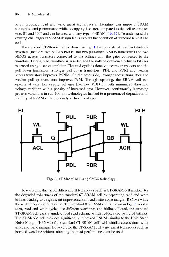
The standard 6T-SRAM cell is shown in Fig. 1 that consists of two back-to-backinverters (includes two pull-up PMOS and two pull-down NMOS transistors) and twoNMOS access transistors connected to the bitlines with the gates connected to thewordline. During read, wordline is asserted and the voltage difference between bitlinesis sensed using a sense amplifier. The read cycle is done via access transistors and thepull-down transistors. Stronger pull-down transistors (PDL and PDR) and weakeraccess transistors improves RSNM. On the other side, stronger access transistors andweaker pull-up transistors improves WM. Through upsizing, the SRAM cell canoperate at very low supply voltages (i.e. low VDDmin) with minimized thresholdvoltage variation with a penalty of increased area. However, continuously increasingprocess variations in sub-100 nm technologies has led to a pronounced degradation instability of SRAM cells especially at lower voltages.
To overcome this issue, different cell techniques such as 8T-SRAM cell amelioratesthe degraded robustness of the standard 6T-SRAM cell by separating read and writebitlines leading to a significant improvement in read static noise margin (RSNM) whilethe write margin is not affected. The standard 8T-SRAM cell is shown in Fig. 2. As it isseen, read and write cycles use different wordlines and bitlines. Noted, the standard8T-SRAM cell uses a single-ended read scheme which reduces the swing of bitlines.The 8T-SRAM cell provides significantly improved RSNM (similar to the Hold StaticNoise Margin (HSNM) of the standard 6T-SRAM cell) with similar access time, writetime, and write margin. However, for the 8T-SRAM cell write assist techniques such asboosted wordline without affecting the read performance can be used.
Fig. 1. 6T-SRAM cell using CMOS technology.
96 F. Moradi et al.

Therefore, proposing a new SRAM cell to improve both read and write marginsunder scaled supply voltages is crucial for ultra-low power applications with lowpenalty on area, access time, and leakage power consumption.
In this chapter, a novel 8T-SRAM cell is presented that improves both read andwrite operation margins. The proposed SRAM cell improves write and read noisemargin by at least 22 % and 2.2X compared to the standard 6T-SRAM cell, respec-tively. Furthermore, this method reduces gate leakage while increases subthresholdleakage compared to the standard 6T-SRAM cell in 65 nm CMOS technology. Ingeneral, leakage power of the proposed cell increases by 67 % at VDD = 1 V and 5.6 %at VDD = 300 mV. The proposed design improves the leakage power by 3 % atVDD = 200 mV. The threshold voltage of the transistors used in this paper is 300 mV.
The rest of this chapter is structured as follows: in Sect. 2, the new 8T-SRAM cellis presented and described in different modes of operation. In Sect. 3, the simulationsresults are presented and discussed. We conclude in Sect. 4.
2 The Proposed 8T-SRAM Cell
Figure 3 shows the proposed 8T-SRAM cell where two transistors, one NMOS and onePMOS are added to the standard 6T-SRAM cell while the mechanism of read issingle-ended [18]. During read, only RWL is asserted while during write both WWLand RWL signals are set to high. In this SRAM cell structure, transistor PUC is used toimprove the write margin of the circuit when a “1” is stored on the storage node Q. Inthis mode, when the value on QB is “0”, the voltage on the drain of NF increases thatweakens the drivability of PUC. Therefore, writing “0” on storage node becomeseasier. When QB keeps “1”, however, the write margin is not expected to be improved.In this case, to improve the write margin of SRAM cell, PUR is sized smaller than PULthat results in an improved write margin in this mode as well. During read, ACL turnson while ACR is kept in cut-off region. When Q holds a “0”, transistors PDL and NF
Fig. 2. Standard 8T-SRAM cell [13].
8T-SRAM Cell with Improved Read and Write Margins 97
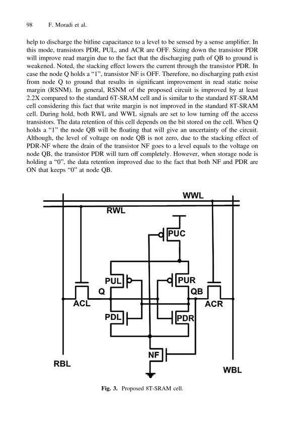
help to discharge the bitline capacitance to a level to be sensed by a sense amplifier. Inthis mode, transistors PDR, PUL, and ACR are OFF. Sizing down the transistor PDRwill improve read margin due to the fact that the discharging path of QB to ground isweakened. Noted, the stacking effect lowers the current through the transistor PDR. Incase the node Q holds a “1”, transistor NF is OFF. Therefore, no discharging path existfrom node Q to ground that results in significant improvement in read static noisemargin (RSNM). In general, RSNM of the proposed circuit is improved by at least2.2X compared to the standard 6T-SRAM cell and is similar to the standard 8T-SRAMcell considering this fact that write margin is not improved in the standard 8T-SRAMcell. During hold, both RWL and WWL signals are set to low turning off the accesstransistors. The data retention of this cell depends on the bit stored on the cell. When Qholds a “1” the node QB will be floating that will give an uncertainty of the circuit.Although, the level of voltage on node QB is not zero, due to the stacking effect ofPDR-NF where the drain of the transistor NF goes to a level equals to the voltage onnode QB, the transistor PDR will turn off completely. However, when storage node isholding a “0”, the data retention improved due to the fact that both NF and PDR areON that keeps “0” at node QB.
Fig. 3. Proposed 8T-SRAM cell.
98 F. Moradi et al.

Similar to the standard 8T-SRAM cell, the proposed cell uses a single-ended readapproach which definitely reduces the swing of the output. However, different tech-niques can be used to compensate this effect such as a pseudo-differential sensingscheme that can be used for our proposed SRAM cell [19].
The simulation results for the circuit for different modes will be discussed in thenext section.
3 Simulation Results and Comparison
Simulation results are done using 65 nm CMOS technology models at room temper-ature (i.e. 27° C) at different supply voltages from subthreshold to superthreshold toregion. In this section, the proposed SRAM cell is simulated at different modes ofoperation.
To evaluate the read stability of an SRAM cell Read Static Noise Margin (RSNM)is used. RSNM is defined as the length of the side of the largest square that can fit intothe lobes of the butterfly curve. Butterfly curve is obtained by drawing and mirroringthe inverter characteristics while access transistors are ON and bitlines are prechargedto VDD [20]. For the proposed SRAM cell, however, only left side of the circuit definesthe stability of the circuit. The reason is attributed to this fact that, when Q holds “1”,increasing the value of QB even to very large values does not change the data stored onnode Q. To this end, we simulate the proposed SRAM cell for cases Q = “0”,WWL = “1”, and RWL = “0” (i.e. CASE 1) and also Q = “1”, WWL = “1”, andRWL = “0” (i.e. CASE 2). The shadowed part of Fig. 4 shows the operation of theproposed SRAM cell when WWL is asserted and RWL signal is low. Here, we con-sider two cases. In CASE 1, node QB discharges via transistor ACR to ground that is asuccessful write while RWL is kept at “0”. However, in CASE 2 where Q holds “1”,although the voltage on node QB increases to 0.4 V, the value on node Q is not flipped.This proves a very high robustness of circuit even at very high input noises when Qstores “1”. This concludes that single ended writing will fail (i.e. CASE 2) that leads usto turn on both access transistors during write cycle. The results for RSNM of theproposed SRAM cell compared to the standard 6T-SRAM cell at different supplyvoltages are shown in Fig. 5. As it is shown, 2.66 X improvements in RSNM isachieved by the use of the proposed 8T-SRAM cell compared to the standard6T-SRAM cell. At lower supply voltages such as 200 mV, the proposed 8T-SRAM cellshows 4.86X improved RSNM. Due to this fact, the proposed SRAM cell is able tooperate with a high margin at very low supply voltages (i.e. subthreshold/weakinversion region). However, the standard 8T-SRAM cell shows slightly better RSNMcompared to the proposed 8T-SRAM cell.
To clarify the operation of the proposed circuit, the SRAM operation at differentmodes is shown in Fig. 6. As it is shown, during read, when Q holds “0”, while the BLhas been discharged to 300 mV, voltage on node Q is not increased higher than 0.2 Vthat is due to the stacking effect of transistors from node QB to ground and the smallsize of the transistor PDR in the cell (Fig. 6(b)). This confirms the robustness ofthe proposed circuit during read (i.e. RSNM). The successful writing “0” is shown inFig. 6(a) when both RWL and WWL are set to high.
8T-SRAM Cell with Improved Read and Write Margins 99

Write margin is another metric used to evaluate the stability of an SRAM cell inwrite mode. Different methods have been used to find the WM of an SRAM cell [21].For the WM simulations, we choose the Word-Line (WL) voltage sweep method. Inthis method the bitline will be connected to the appropriate voltages to enable flipping
Fig. 4. Waveforms of the proposed 8T-SRAM cell (Shadowed part shows when WWL = “1”and QB = 1 or “0”).
Fig. 5. RSNM results for the standard 6T-SRAM, 8T-SRAM and the proposed 8T-SRAM cell.
100 F. Moradi et al.
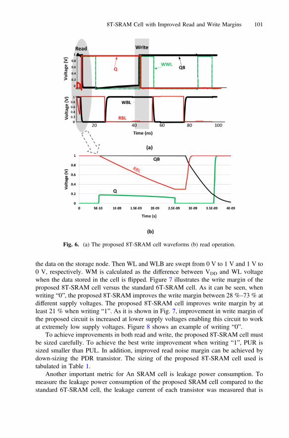
the data on the storage node. Then WL and WLB are swept from 0 V to 1 V and 1 V to0 V, respectively. WM is calculated as the difference between VDD and WL voltagewhen the data stored in the cell is flipped. Figure 7 illustrates the write margin of theproposed 8T-SRAM cell versus the standard 6T-SRAM cell. As it can be seen, whenwriting “0”, the proposed 8T-SRAM improves the write margin between 28 %–73 % atdifferent supply voltages. The proposed 8T-SRAM cell improves write margin by atleast 21 % when writing “1”. As it is shown in Fig. 7, improvement in write margin ofthe proposed circuit is increased at lower supply voltages enabling this circuit to workat extremely low supply voltages. Figure 8 shows an example of writing “0”.
To achieve improvements in both read and write, the proposed 8T-SRAM cell mustbe sized carefully. To achieve the best write improvement when writing “1”, PUR issized smaller than PUL. In addition, improved read noise margin can be achieved bydown-sizing the PDR transistor. The sizing of the proposed 8T-SRAM cell used istabulated in Table 1.
Another important metric for An SRAM cell is leakage power consumption. Tomeasure the leakage power consumption of the proposed SRAM cell compared to thestandard 6T-SRAM cell, the leakage current of each transistor was measured that is
Fig. 6. (a) The proposed 8T-SRAM cell waveforms (b) read operation.
8T-SRAM Cell with Improved Read and Write Margins 101

shown in Table 2. As it is shown the leakage through access transistors is reducedsignificantly that is attributed to the raised voltage level of storage node holding “0”.However, the total leakage current of the proposed cell is increased when the stored bitis “1” while in case of Q = “0”, the total leakage of the proposed cell is less than thestandard 6T and 8T-SRAM cells. For this simulation a bitline capacitance of 200fF andthe supply voltage of VDD equals to 1 V at room temperature have been considered. Toshow the power degradation of the proposed SRAM cell at different supply voltage, wecalculate the total power consumption of the proposed cell versus the standard6T-SRAM and 8T-SRAM cells for VDD = 1 V to VDD = 200 mV. As it is shown inFig. 9, leakage power of the proposed SRAM cell compared to the standard 6T-SRAMcell is degraded by 14.2 % and 67 % for supply voltages of 0.2 V and 1 V, respectivelywhen the stored bit is “0” while for the case of Q=“1”, the proposed cell improves theleakage power by 34 % and 23 % at supply voltage of 1 V and 0.4 V, respectively. Incomparison to the standard 8T-SRAM cell for the case of Q = “1”, leakage current isdegraded by 7 % to 21 % for VDD = 0.2 V and 1 V, respectively while for the case ofQ = “0”, the leakage current of the proposed cell increases by 20 % and 43 % forVDD = 0.2 V and 1 V, respectively.
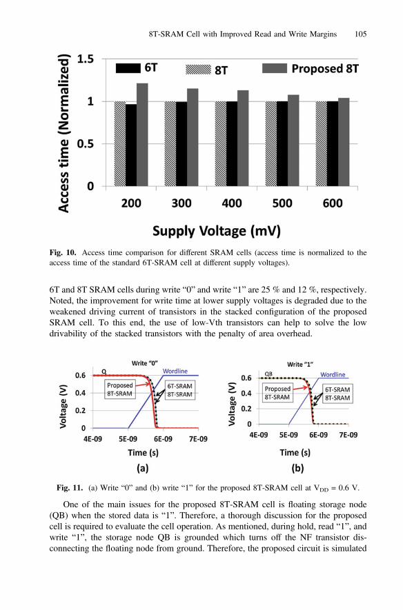
In this part, the access time and the write time of the proposed circuit is explored incomparison with the standard 6T and 8T-SRAM cells [6]. Access time is measured asthe time required for discharging the bitline voltage so that the difference betweenbitline voltage and VDD (i.e. Vsense) can be sensed by the sense amplifier circuit. To thisend, we simulate the proposed 8T-SRAM cell at supply voltage of VDD = 300 mV atroom temperature. Figure 10 illustrates the comparison between the proposed8T-SRAM cell versus standard 6T-SRAM and the 8T-SRAM cells. As it is seen, the
Fig. 7. Write margin of the proposed 8T-SRAM cell versus the standard 6T-SRAM cell whenwriting “0” and “1” (the standard 8T-SRAM provide negligibly smaller WM in comparison tothe standard 6T-SRAM cell).
102 F. Moradi et al.

maximum degradation is at lower supply voltage due to the weakened drivability of thetransistors at lower supply voltages. The maximum degradation is at 200 mV (21 %)which improved by increasing the supply voltage. For instance, at VDD = 600 mV, theaccess time degradation is only 4 % compared to the standard 6T and 8T-SRAM cellsand all the circuit show similar access time at VDD = 800 mV and above.
Fig. 8. Write “0” for the proposed 8T-SRAM cell.
Table 1. Sizing of the standard 6T, 8T and the proposed 8T-SRAM cells.
6T-SRAM cell Proposed8T-SRAM
Standard8T-SRAM
ACL, ACR 180n ACL, ACR 180n ACL, ACR 180nPDR 230n PDR 200n PDR,PDL 200nPUL 230n PUL 150n PUL 150nPUR, PDR 150n PUR 120n PUR 150n
PUC 150n R1 180nPDL, NF 300n R2 230n
8T-SRAM Cell with Improved Read and Write Margins 103

Another metric to compare different SRAM topologies is write time. In the pro-posed circuit due to the increased write margin, it is expected a faster data flipping onstorage nodes during write cycle. Due to the asymmetry nature of the proposed SRAMcell, we simulate the cell for write “0” and write “1”. Figure 11(a) and (b) illustrate theproposed SRAM cell behavior for both cases. As it is seen, the proposed SRAM cellprovides faster write during write “0” compared to write “1” that is attributed to theweakened pull-up path through which the contention between PMOSs and accesstransistors is reduced. Figure 12 shows a comparison between the proposed SRAM cellversus the standard 6T and 8T SRAM cells at supply voltage of 600 mV. Here, thewrite time improvement percentages provided by the proposed cell over the standard
Table 2. The leakage current of the standard 6T and the proposed 8T SRAM cells.
6T-SRAM Current (nA).G:gate, D: Drain, and S:
Source
Proposed 8T-SRAM Current (nA). G:gate, D: Drain, and S:
Source
Standard 8T-SRAM Current (nA). G:gate, D: Drain, and S:
SourceTr. G D S Tr. G D S Tr G D S
ACL 0.323 0.017 0.15 ACL 0.36 0.084 0.209 ACL 0.1 1.3 1.16ACR 0.153 1.802 1.853 ACR 0.144 0.178 0.187 ACR 0.23 0.098 0.104PUL 0.563 4.191 4.767 PUL 0.462 2.95 3.428 PUL 0.115 1.13 1.01PUR 0.208 1.856 1.66 PUR 0.122 1.132 0.979 PUR 0.31 2.69 2.68PDL 0.234 2.361 2.103 PDL 0.246 1.497 1.73 PDL 0.52 2.72 3.24PDR 1.47 4.455 5.892 PDR 0.887 3 2.02 PDR 0.114 1.37 1.24
PUC 0.47 4.42 4.896 R1 1.10 3.90 1.13NF 0.001 4.967 5.025 R2 0.57 1.02 0.075
Fig. 9. Leakage power increase percentage for proposed 8T-SRAM cell versus the standard6T-SRAM cell.
104 F. Moradi et al.
6T and 8T SRAM cells during write “0” and write “1” are 25 % and 12 %, respectively.Noted, the improvement for write time at lower supply voltages is degraded due to theweakened driving current of transistors in the stacked configuration of the proposedSRAM cell. To this end, the use of low-Vth transistors can help to solve the lowdrivability of the stacked transistors with the penalty of area overhead.
One of the main issues for the proposed 8T-SRAM cell is floating storage node(QB) when the stored data is “1”. Therefore, a thorough discussion for the proposedcell is required to evaluate the cell operation. As mentioned, during hold, read “1”, andwrite “1”, the storage node QB is grounded which turns off the NF transistor dis-connecting the floating node from ground. Therefore, the proposed circuit is simulated
Fig. 10. Access time comparison for different SRAM cells (access time is normalized to theaccess time of the standard 6T-SRAM cell at different supply voltages).
Fig. 11. (a) Write “0” and (b) write “1” for the proposed 8T-SRAM cell at VDD = 0.6 V.
8T-SRAM Cell with Improved Read and Write Margins 105

for each cycle. During hold, the drain of NF is charged to a voltage equals to 53.5 mVwhich is equals to the voltage on node QB. The circuit was simulated for a long stay inhold time which shows the voltage on nodes QB and the drain of NF becomes equaland fixed at 53.5 mV. This leads to a turned-off transistor PDR which reduces theleakage current through storage node to ground. All three SRAM cells were simulatedto measure their leakage current through storage nodes to ground under same condition.
Fig. 12. Write time comparison between the standard 6T and 8T SRAM cells with the proposed8T-SRAM cell.
Fig. 13. Write power consumption for different SRAM cells.
106 F. Moradi et al.

During hold, we measured the leakage through transistors connected to ground to getan estimation of the total leakage when the node QB is floating. Simulation resultsshow a fixed leakage current of 1.72 nA through pull-down transistors to ground whilethe standard 6T and 8T SRAM cells show a total leakage current of 2.59 nA and2.63 nA through transistors connected to ground, respectively. However, as shownbefore, the total leakage power of the proposed circuit is higher than as for the standard6T-SRAM cell when the stored data is “0”.
During write “0”, as explained in Sect. 2, the QB node is floating which helps toimprove the write margin and write time. Based on this fact, the total write power isreduced, as well. To this end, the total power consumption of the standard 6T and 8T iscompared with the proposed 8T-SRAM cell which is shown in Fig. 13. As it is seen,the proposed design provides minimum write power consumption during write “0”which is attributed to the floating node QB and drain of transistor NF.
During read due to the single-ended structure of the proposed circuit in which thenode QB is decoupled from bitline, it will not affect the read process. Assuming that the
Fig. 14. Write power consumption for different SRAM cells.
8T-SRAM Cell with Improved Read and Write Margins 107

voltage on node QB is 53.5 mV, it will continue to keep this voltage during read, aswell. To evaluate the cells during read “1”, the read power consumption of each circuitwas measured. The standard 6T and 8T SRAM cells consume a read power of119.46 nW and 1.9758 nW, respectively, while the proposed 8T-SRAM consumes0.93 nW (930 pW). Consequently, we can claim that the floating node QB has no effecton the performance as well as it improves the power consumption during read and write.
Finally, the area of the proposed circuit in comparison to the standard 6T-SRAMcell is shown for a single cell. As it is shown in Fig. 14, the proposed techniqueincreases the area by 49 % in comparison the standard 6T-SRAM cell. However, due tothe L-shape of the cell layout, the total area overhead of the cell will be reduced. Thestandard 8T-SRAM cell, however, introduces 33 % area overhead in TSMC 65 nmtechnology.
All in all, the proposed SRAM cell, similar to the standard 8T-SRAM cell,improves read margin significantly while the write margin is improved, as well.Therefore, the proposed design has the advantages of improved write margin andwrite-time over the standard 6T and 8T-SRAM cells. Due to the asymmetric nature ofthe proposed SRAM cell, write margin improvement when writing “0” is larger thanthe case of “1”. Therefore, as mentioned, by careful sizing of the transistors in ourdesign, higher write margin (i.e. more symmetric write) will be achieved that enablesdesigners to scale the supply voltage aggressively for ultra-low power applications.
4 Conclusions
In this chapter, a new 8T-SRAM cell was discussed which shows improvement in readand write margins by 2.2X and 22 %, respectively, compared to the standard6T-SRAM cell. In addition, the proposed design improves the gate leakage powerconsumption while increases the subthreshold leakage compared to the 6T-SRAM cell.All in all, the proposed design improves read and write margins without any penalty inleakage power at subthreshold region compared to the standard 6T-SRAM cell. Fur-thermore, the proposed 8T-SRAM cell has a superior advantage of improved writemargin in comparison to the standard 8T-SRAM cell.
References
1. Horowitz, M.: Scaling, power, and the future of MOS. In: IEDM Technical Digest, pp. 9–15,December 2005
2. Moradi, F., Gupta, S.K., Panagopoulos, G., Wisland, D.T., Mahmoodi, H., Roy, K.:Asymmetrically doped FinFETs for low-power robust SRAMs. IEEE Trans. ElectronDevices 58(12), 4241–4249 (2011)
3. Collaert, N., De Keersgieter, A., Dixit, A., Ferain, I., Lai, L.-S., Lenoble, D., Mercha, A.,Nackaerts, A., Pawlak, B.J., Rooyackers, R., Schulz, T., Sar, K.T., Son, N.J., Van Dal, M.J.H., Verheyen, P., von Arnim, K., Witters, L., De, M., Biesemans, S., Jurczak, M.: Multi-gatedevices for the 32 nm technology node and beyond. In: Proceedings of 37th ESSDERC,pp. 143–146, 11–13 September 2007
108 F. Moradi et al.
4. Sachid, A.B., Hu, C.: Denser and more stable SRAM using FinFETs with multiple finheights. IEEE Trans. Electron Devices 59(8), 2037–2041 (2012)
5. Tawfik, S.A., Kursun, V.: Multi-threshold voltage FinFET sequential circuits. IEEE Trans.VLSI Syst. 19(1), 151–156 (2011)
6. Verma, N., Chandrakasan, A.: A 256 kb 65 nm 8T subthreshold SRAM employingsense-amplifier redundancy. IEEE J. Solid-State Circuits 43(1), 141–149 (2008)
7. Aly, R.E., Bayoumi, M.A.: Low-power cache design using 7T SRAM cell. IEEE Trans.Circuits Syst. II, Exp. Briefs 54(4), 318–322 (2007)
8. Madiwalar, B., Kariyappa, B.S.: Single bit-line 7T SRAM cell for low power and highSNM. In: International Multi-Conference on iMac4s, pp. 223–228, March 2013
9. Wen, L., Li, Z., Li, Y.: Differential-read 8T SRAM cell with tunable access and pull-downtransistors. Electron. Lett. 48(20), 1260–1261 (2012)
10. Tu, M.H., Lin, J.-Y., Tsai, M.-C., Lu, C.-Y., Lin, Y.-J., Wang, M.-H., Huang, H.-S., Lee,K.-D., Shih, W.-C., Jou, S.-J., Chuang, C.-T.: A single-ended disturb-free 9T subthresholdSRAM with cross-point data-aware write word-line structure, negative bit-line, and adaptiveread operation timing tracing. IEEE J. Solid-State Circuits 47(6), 1469–1482 (2012)
11. Chang, I.J., Kim, J., Park, S.P., Roy, K.: A 32 kb 10T sub-threshold SRAM array withbit-interleaving and differential read scheme in 90 nm CMOS. IEEE J. Solid State Circuits44(2), 650–658 (2009)
12. Moradi, F., Wisland, D.T., Aunet, S., Mahmoodi, H., Tuan Vu, C.: 65 nm sub-threshold11T-SRAM for ultra-low voltage applications. In: SOC Conference, IEEE International,pp. 113–118 (2008)
13. Calhoun, B.H., Chandrakasan, A.P.: Static noise margin variation for sub-threshold SRAMin 65 nm CMOS. IEEE J. Solid-State Circuits 41, 1673–1679 (2006)
14. Moradi, F., Madsen, J.K.: Robust subthreshold 7T-SRAM cell for low-power applications.In: IEEE Midwest Symposium on Circuits and Systems (MWSCAS), pp. 893, 896, 3–6August 2014
15. Moradi, F., Madsen, J.K.: Improved read and write margins using a novel 8T-SRAM cell.In: International Conference on Very Large Scale Integration (VLSI-SoC), pp. 1, 5, 6–8October 2014
16. Moradi, F., Wisland, D.T., Mahmoodi, H., Berg, Y., Cao, T.V.: New SRAM design usingbody bias technique for ultra-low power applications. In: 11th International Symposium onQuality Electronic Design (ISQED), pp. 468, 471, 22–24 March 2010
17. Farkhani, H., Peiravi, A., Moradi, F.: A new asymmetric 6T SRAM cell with a write assisttechnique in 65 nm CMOS technology. Microelectronics Journal 45, 1556–1565 (2014)
18. Moradi, F., Madsen, J.K.: Improved read and write margins using a novel 8T-SRAM cell.In: 2014 22nd International Conference on Very Large Scale Integration (VLSI-SoC), pp. 1,5, 6–8 October 2014
19. Nalam, S., Chandra, V., Pietrzyk, C., Aitken, R., Calhoun, B.: Asymmetric 6T SRAM withtwo-phase write and split bitline differential sensing for low voltage operation. In:Proceedings 11th International Symposium Quality Electronic Design (ISQED), pp. 139–146, March 2010
20. Seevinck, E., List, F.J., Lohstroh, J.: Static-noise margin analysis of MOS SRAM cells.IEEE J. Solid-State Circuits 22, 748–754 (1987)
21. Wang, J., Nalam, S., Calhoun, B.H.: Analyzing static and dynamic write margin fornanometer SRAMs. In: Proceedings of International Symposium Low Power Electron.Design, pp. 129–134, New York (2008)
8T-SRAM Cell with Improved Read and Write Margins 109