±8g 2 axis accelerometer with programmable vibration filter · ±8g 2 axis accelerometer with...
TRANSCRIPT
MEMSIC MXC6244AU Rev.C Page 1 of 15 Formal release date: 11/16/2016
±8g 2 Axis Accelerometer with Programmable Vibration Filter
MXC6244AU FEATURES High accuracy 2-axis accelerometer:
o 8g FSR, 1mg/LSB resolution o 0.3 mg/C offset drift over
temperature o 0.5% Sensitivity matching over
temperature Programmable anti-vibration filter
o Attenuation >60dB @ 50Hz o No sensor resonance
Internal angle detection circuit with 8 programmable thresholds and INT output
400kHz I2C Interface (1.8V compatible) Built-in self-test functionality Small, 6-pin 3 x 3 x 1 mm LCC package Operates from 2.7 V to 5.5 V Supply High reliability automotive process and
package RoHS compliant Operates from -40C to +125C
APPLICATIONS Inclination Sensing in High Vibration
Environments Motorcycle Fall-Down Detection Off-Road Vehicle Roll Detection Jet Ski Roll Detection General Purpose Acceleration Measurements
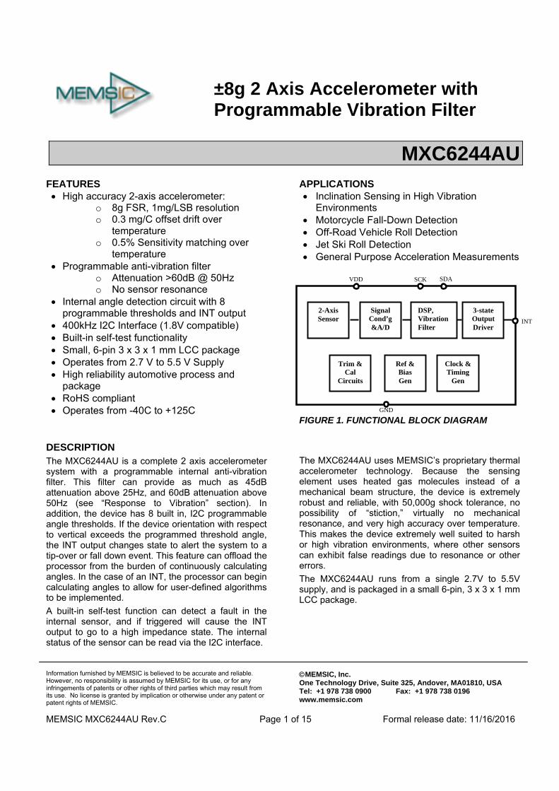
FIGURE 1. FUNCTIONAL BLOCK DIAGRAM
DESCRIPTION The MXC6244AU is a complete 2 axis accelerometer system with a programmable internal anti-vibration filter. This filter can provide as much as 45dB attenuation above 25Hz, and 60dB attenuation above 50Hz (see “Response to Vibration” section). In addition, the device has 8 built in, I2C programmable angle thresholds. If the device orientation with respect to vertical exceeds the programmed threshold angle, the INT output changes state to alert the system to a tip-over or fall down event. This feature can offload the processor from the burden of continuously calculating angles. In the case of an INT, the processor can begin calculating angles to allow for user-defined algorithms to be implemented.
A built-in self-test function can detect a fault in the internal sensor, and if triggered will cause the INT output to go to a high impedance state. The internal status of the sensor can be read via the I2C interface.
The MXC6244AU uses MEMSIC’s proprietary thermal accelerometer technology. Because the sensing element uses heated gas molecules instead of a mechanical beam structure, the device is extremely robust and reliable, with 50,000g shock tolerance, no possibility of “stiction,” virtually no mechanical resonance, and very high accuracy over temperature. This makes the device extremely well suited to harsh or high vibration environments, where other sensors can exhibit false readings due to resonance or other errors.
The MXC6244AU runs from a single 2.7V to 5.5V supply, and is packaged in a small 6-pin, 3 x 3 x 1 mm LCC package.
Information furnished by MEMSIC is believed to be accurate and reliable. However, no responsibility is assumed by MEMSIC for its use, or for any infringements of patents or other rights of third parties which may result from its use. No license is granted by implication or otherwise under any patent or patent rights of MEMSIC.
MEMSIC, Inc. One Technology Drive, Suite 325, Andover, MA01810, USA Tel: +1 978 738 0900 Fax: +1 978 738 0196 www.memsic.com
2-Axis Sensor INT
Signal Cond’g &A/D
DSP, Vibration Filter
3-state Output Driver
Ref & Bias Gen
Clock & Timing
Gen
Trim & Cal
Circuits
VDD SDA
GND
SCK

MEMSIC MXC6244AU Rev.C Page 2 of 15 Formal release date: 11/16/2016
SENSOR CHARACTERISTICS: (TA=25C, VDD= 5V, Fs=3125Hz, unless otherwise specified. Typical values are specified at 25C)
Parameter Conditions Min Typ Max Units
Full Scale Range 8 g
Sensitivity
TA=25C 975 1024 1075 LSB/g
Temperature Drift (-40 to +85C) ±6 ±8.51 %
X/Y Matching over Temperature (-40 to +85C) ±0.3 ±0.51,5 %
Zero-g Bias TA=25C ±10 ±301 mg
Temperature Drift (-40 to +85C) ±0.1 ±0.31 mg/C
Threshold Angles Programmable via I2C
40, 42.5, 45, 50, 55, 60, 65, 70
Deg
Threshold Accuracy ±4 Deg
Sensor Bandwidth (Note 2) 11 Hz
Input Referred Noise Total RMS Noise, ODR = 1.5Hz 0.75
mg rms Total RMS Noise, ODR = 100Hz 1.5
Offset shift when self-test is asserted
X-offset (ST[2:0]=111) +2 g
Y-offset (ST[2:0]=111) -2
Resonance (Note 3) Undetectable Hz
LOW-g Lockout Threshold (Note 4) ±0.375 g
Note 1: Established statistically as the average value ±3 standard deviations from 30 pieces x 3 lot characterization data Note 2: The sensor has an inherent low pass filter characteristic which is very effective in attenuating out of band vibration. Note 3: The thermal accelerometer sensors use heated gas molecules, and have no measurable resonance Note 4: The LOW-G Lockout feature disables tip-over detection if the magnitude of both X and Y acceleration vectors fall below 0.375g (as in
the case of a free-fall or large off-axis tilt condition). See also “Fault Detection”. Note 5: Indicates how closely X and Y axis sensitivities’ change over temperature.
MEMSIC MXC6244AU Rev.C Page 3 of 15 Formal release date: 11/16/2016
ELECTRICAL SPECIFICATIONS: (TA=25C, VDD= 5V, Fs=3125Hz, unless otherwise specified. Typical values are specified at 25C)
Parameter Conditions Min Typ Max Units
Supply Voltage 2.7 5.5 V
Supply Current Operating Mode 1.3 3 mA
Sleep Mode 0.2 1 uA
Operating Temperature -40 125 C
A/D Sample Frequency (Fs) Programmable via I2C 3.1, 6.2, 12.5, 25, 50, 100
kHz Output Data Rate (ODR)
Angle Detection Enabled Fs/2048
Angle Detection Disabled Fs/1024
Wake Time (After exiting Sleep mode) 300 500 ms
Power On Time (After Vdd Rising Edge) 300 500 ms
Power On Reset Threshold 0.8 1.2 1.6 V
VDD Rise Time (Note 6) 8 ms Note 6: Maximum allowable power supply rise time from 0.25V to 2.5V (minimum). Slower VDD rise time may cause erroneous data retrieval
from OTP memory at power-up DIGITAL PARAMETERS (Note 7) (TA=25C, VDD= 5V, unless otherwise specified. Typical values are specified at 25C)
Parameter Conditions Min Typ Max Units
Logic Input Low SDA, SCK Inputs 0 0.3*VIO V
Logic Input High SDA, SCK Inputs 0.7*VIO VIO V
Logic Output Low SDA, INT, Sinking 0.5mA (Note 8) 0.1*VIO V
Logic Output High INT, Sourcing 0.5mA (Note 8) 0.9*VIO 1.1*VIO
Logic Output High-Z INT, After sensor fault is detected 1 Mohm Note 7: VIO is automatically detected using a peak-hold circuit on the SCK pin. The SCK or SDA voltage should not remain in the LOW state for
more than 10ms. Note 8: The output driver is capable of sourcing and sinking much higher currents, but it is recommended to keep the load current below 0.5mA
to avoid thermal gradients which may affect the angle threshold accuracy.
DIGITAL SWITCHING CHARACTERISTICS (TA=25C, VDD= 5V, unless otherwise specified. Typical values are specified at 25C)
Parameter Symbol Min Typ Max Units
Operating Valid Time (Note 9) tOP 30 ms
SCK Clock Frequency fSCK 0.1 400 kHz
Rise Time tR 0.3 µs
Fall Time tF 0.3 µs
SCK Low Time tLOW 1.3 µs
SCK High Time tHIGH 0.6 µs
SDA Setup Time tSU;D 0.1 µs
SDA Hold Time tH;D 0 0.9 µs
Start Setup Time tSU;S 0.6 µs
Start Hold Time tH;S 0.6 µs
Stop Setup Time tSU;P 0.6 µs
Bus Free Time tBF 1.3 µs Note 9: This is the wait time after VDD applied to communicate successfully over I2C interface.

MEMSIC MXC6244AU Rev.C Page 4 of 15 Formal release date: 11/16/2016
ABSOLUTE MAXIMUM RATINGS* Supply Voltage (VDD) ………………………..-0.5 to +7V Storage Temperature …..….…………-40C to +150C *Stresses above those listed under Absolute Maximum Ratings may cause permanent damage to the device. This is a stress rating only; the functional operation of the device at these or any other conditions above those indicated in the operational sections of this specification is not implied. Exposure to absolute maximum rating conditions for extended periods may affect the device’s reliability.
PIN DESCRIPTION: LCC-6 Package Pin Name Description I/O 1 INT Interrupt Output. This pin will
be low under normal operation, and will transition to high to alert to a tip-over event. A high impedance state reflects a fault condition in the sensor. This pin can be left open if not used.
O
2 NC Factory Use, connect to ground
3 VDD Positive power supply. Connect to 2.7V to 5.5V. Bypass this to ground using a tbd capacitor
P
4 SCK I2C clock input I 5 SDA I2C data pin (input/output) I/O 6 GND Connect to power supply
ground. P
RESPONSE TO VIBRATION The MXC6244AU is unique in its vibration rejection characteristics, due both to its sensor structure, and its signal processing features. The MXC6244AU uses MEMSIC’s proprietary thermal MEMS acceleration sensor, which uses heated gas molecules in a sealed cavity. This technology offers two distinct benefits: (a) The sensor has no detectable resonance, and (b) The sensor has an inherent low-pass frequency response, which provides very effective filtering of unwanted vibration signals prior to the electronic signal path. Additional filtering is provided by a digital second order comb filter, which enables the device to tolerate very high levels of out-of-band vibration with negligible effect on angle detection accuracy. This digital vibration filter is programmable via the I2C interface. The table below shows the tradeoffs among A/D clock rate (Fs), Output Data Rate (ODR), and the vibration attenuation at selected frequencies.
Fs (kHz)ODR (Hz)
Vibration Attenuation (dB) 50Hz 100Hz 300Hz
100 48.8
See Plots Below
50 24.4 25 12.2
12.5 6.1 6.25 3 3.125 1.5
The following plots show the attenuation vs. vibration frequency, swept from 10Hz to 1000Hz, at the 6 different filter clock settings. The combined attenuation (A) due to the low-pass characteristic of the sensor and the comb filter can be expressed as
20 ∗ log1
1 12
∗1512
∗sin ∗ 512 ∗
sin ∗
Where A is attenuation in dB, and f is the vibration frequency in Hz.
Attenuation vs. Vibration Frequency
Fclk = 3.125kHz
Attenuation vs. Vibration Frequency
Fclk = 6.25kHz
‐200
‐150
‐100
‐50
0
10 100 1000
Vibration Attenuation (dB)
Total …
‐200
‐150
‐100
‐50
0
10 100 1000
Vibration Attenuation (dB)
Total …
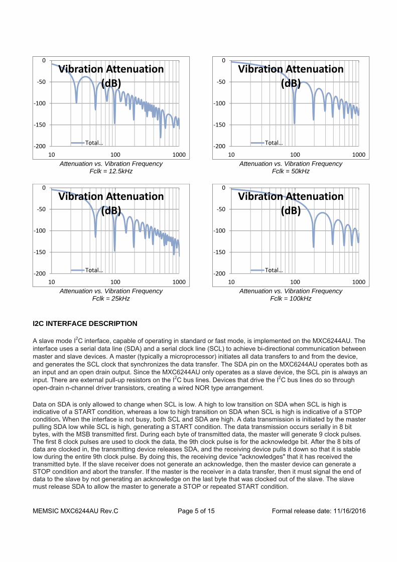
MEMSIC MXC6244AU Rev.C Page 5 of 15 Formal release date: 11/16/2016
Attenuation vs. Vibration Frequency
Fclk = 12.5kHz
Attenuation vs. Vibration Frequency
Fclk = 25kHz
Attenuation vs. Vibration Frequency
Fclk = 50kHz
Attenuation vs. Vibration Frequency
Fclk = 100kHz
I2C INTERFACE DESCRIPTION
A slave mode I2C interface, capable of operating in standard or fast mode, is implemented on the MXC6244AU. The interface uses a serial data line (SDA) and a serial clock line (SCL) to achieve bi-directional communication between master and slave devices. A master (typically a microprocessor) initiates all data transfers to and from the device, and generates the SCL clock that synchronizes the data transfer. The SDA pin on the MXC6244AU operates both as an input and an open drain output. Since the MXC6244AU only operates as a slave device, the SCL pin is always an input. There are external pull-up resistors on the I2C bus lines. Devices that drive the I2C bus lines do so through open-drain n-channel driver transistors, creating a wired NOR type arrangement.
Data on SDA is only allowed to change when SCL is low. A high to low transition on SDA when SCL is high is indicative of a START condition, whereas a low to high transition on SDA when SCL is high is indicative of a STOP condition. When the interface is not busy, both SCL and SDA are high. A data transmission is initiated by the master pulling SDA low while SCL is high, generating a START condition. The data transmission occurs serially in 8 bit bytes, with the MSB transmitted first. During each byte of transmitted data, the master will generate 9 clock pulses. The first 8 clock pulses are used to clock the data, the 9th clock pulse is for the acknowledge bit. After the 8 bits of data are clocked in, the transmitting device releases SDA, and the receiving device pulls it down so that it is stable low during the entire 9th clock pulse. By doing this, the receiving device "acknowledges" that it has received the transmitted byte. If the slave receiver does not generate an acknowledge, then the master device can generate a STOP condition and abort the transfer. If the master is the receiver in a data transfer, then it must signal the end of data to the slave by not generating an acknowledge on the last byte that was clocked out of the slave. The slave must release SDA to allow the master to generate a STOP or repeated START condition.
‐200
‐150
‐100
‐50
0
10 100 1000
Vibration Attenuation (dB)
Total …
‐200
‐150
‐100
‐50
0
10 100 1000
Vibration Attenuation (dB)
Total …
‐200
‐150
‐100
‐50
0
10 100 1000
Vibration Attenuation (dB)
Total …
‐200
‐150
‐100
‐50
0
10 100 1000
Vibration Attenuation (dB)
Total …

MEMSIC MXC6244AU Rev.C Page 6 of 15 Formal release date: 11/16/2016
The master initiates a data transfer by generating a START condition. After a data transmission is complete, the master may terminate the data transfer by generating a STOP condition. The bus is considered to be free again a certain time after the STOP condition. Alternatively, the master can keep the bus busy by generating a repeated START condition instead of a STOP condition. This repeated START condition is functionally identical to a START condition that follows a STOP. Each device that sits on the I2C bus has a unique 7-bit address.
The first byte transmitted by the master following a START is used to address the slave device. The first 7 bits contain the address of the slave device, and the 8th bit is the R/W* bit (read = 1, write = 0; the asterisk indicates active low, and is used instead of a bar). If the transmitted address matches up to that of the MXC6244AU, then the MXC6244AU will acknowledge receipt of the address, and prepare to receive or send data.
If the master is writing to the MXC6244AU, then the next byte that the MXC6244AU receives, following the address byte, is loaded into the address counter internal to the MXC6244AU. The contents of the address counter indicate which register on the MXC6244AU is being accessed. If the master now wants to write data to the MXC6244AU, it just continues to send 8-bit bytes. Each byte of data is latched into the register on the MXC6244AU that the address counter points to. The address counter is incremented after the transmission of each byte.
If the master wants to read data from the MXC6244AU, it first needs to write the address of the register it wants to begin reading data from to the MXC6244AU address counter. It does this by generating a START, followed by the address byte containing the MXC6244AU address, with R/W* = 0. The next transmitted byte is then loaded into the MXC6244AU address counter. Then, the master repeats the START condition and re-transmits the MXC6244AU address, but this time with the R/W* bit set to 1. During the next transmission period, a byte of data from the MXC6244AU register that is addressed by the contents of the address counter will be transmitted from the MXC6244AU to the master. As in the case of the master writing to the MXC6244AU, the contents of the address counter will be incremented after the transmission of each byte. The protocol for multiple byte reads and writes between a master and a slave device is depicted in FIGURE 2.
FIGURE 2.
The 7-bit I2C address for MXC6244AU is set as 0010100b (0x14).

MEMSIC MXC6244AU Rev.C Page 7 of 15 Formal release date: 11/16/2016
MXC6244AU I2C interface allows I2C interface voltage VIO to be lower than the supply voltage VDD. VIO can be as low as 1.65 V. In order to achieve reliable operation, avoid the situation when both SCL and SDA pins are low for longer than 10ms. Please contact Memsic if you plan on using I2C interface voltage VIO greater than VDD.
I2C REGISTER DEFINITION The MXC6244AU has 10 user-accessible registers which are identified and summarized in the table below.
Address Name Definition Access $00 XOUT0 Lower 8 bits of X acceleration output read $01 XOUT1 Higher bits of 14-bit X output read $02 YOUT0 Lower 8 bits of Y acceleration output read $03 YOUT1 Higher bits of 14-bit Y output read $06 STATUS Orientation and status read $07 Detection Several control signals write $08 Factory 8 Factory use only n/a $09 Factory 9 Factory use only n/a $0A CLK_CONT Controls ADC clock and ODR write $10 Who_Am_I Allows electronic identification read
User Register Summary
Following is a more detailed description of the contents and function of each Register.
Register $00: XOUT0 – Lower 8 bits of x-axis acceleration output (read only)
D7 D6 D5 D4 D3 D2 D1 D0 XOUT[7] XOUT[6] XOUT[5] XOUT[4] XOUT[3] XOUT[2] XOUT[1] XOUT[0]
Register $01: XOUT1 – Upper 6 bits of x-axis acceleration output (read only)
D7 D6 D5 D4 D3 D2 D1 D0 0 0 XOUT[13] XOUT[12] XOUT[11] XOUT[10] XOUT[9] XOUT[8]
The number of bits in XOUT is fixed at 14 bits. Output is presented in 2’s complement format. Bits 6 and 7 of register $01 are always zeroes.
Register $02: YOUT0 – Lower 8 bits of y-axis acceleration output (read only)
D7 D6 D5 D4 D3 D2 D1 D0 YOUT[7] YOUT[6] YOUT[5] YOUT[4] YOUT[3] YOUT[2] YOUT[1] YOUT[0]
Register $03: YOUT1 – Upper 6 bits of y-axis acceleration output (read only)
D7 D6 D5 D4 D3 D2 D1 D0 0 0 YOUT[13] YOUT[12] YOUT[11] YOUT[10] YOUT[9] YOUT[8]
The number of bits in YOUT is fixed at 14 bits. Output is presented in 2’s complement format. Bits 6 and 7 of register $03 are always zeroes.
Register $06: STATUS –status register (read only)
D7 D6 D5 D4 D3 D2 D1 D0 INT CRC_OK FAIL TILT ORI[1] ORI[0] OR[1] OR[0]
Note: OR[1:0] is a 2-bit indication of the device orientation, according to the following scheme: OR[1:0] = 00 – device is oriented in Region 1 (see FIGURE 3 below titled “Orientation Regions”); OR[1:0] = 01 – device is in Region 2 (vertical in upright orientation); OR[1:0] = 10 – device is in Region 3; OR[1:0] = 11 – device is in Region 4 (vertical in inverted orientation). The bits OR[1:0] are indicative of “long-term” orientation when anti-dithering circuit is used. The orientation is determined by measuring the quantities A*ax – B*ay, and A*ax + B*ay and comparing results to zero. The coefficients A and B are defined internally based on selected threshold angle. In addition to these measurements, the orientation measurement must be validated by requiring that the larger in magnitude of ax, ay be

MEMSIC MXC6244AU Rev.C Page 8 of 15 Formal release date: 11/16/2016
greater than 3/8 g. When anti-dithering circuit is enabled in order for a new value of OR[1:0] to be written to the STATUS register, a valid measurement of the new orientation must be measured 16 consecutive times. This provides a low-pass filtering and hysteresis effect that keeps a display from flickering near orientation boundaries. If anti-dithering circuit is not enabled the OR[1:0] bits are the same as ORI[1:0]. Enabling anti-dithering circuit at low ADC clock frequency may result in very slow detection time.
ORI[1:0] is the instantaneous device orientation. It follows the same scheme as OR[1:0], except that it is updated every time a valid orientation measurement is made, not subject to the same anti-dithering filtering as OR[1:0].
TILT is an indication of whether there is enough acceleration signal strength to make a valid orientation measurement. If TILT = 0, the orientation measurement is valid, if TILT = 1, then the orientation measurement is invalid. TILT is updated every measurement cycle.
FAIL is an indication whether one of the two built-in self-test checks has failed. See section Internal Fault Detection for description of the internal self-test checks. The OTP failure (CRC check failed) is not indicated by this bit, only checks (b), and (c), defined in the Internal Fault Detection section are indicated by this bit. FAIL bit being high does not necessarily mean the device is bad, just that it is reading unexpected acceleration values.
CRC_OK is an indicator that OTP memory has loaded correctly and passed the CRC check. It transitions high approximately 10ms after power-up. If this bit stays low it is an indication of OTP memory failure. The part should not be trusted in such condition. It is recommended to read this bit 50ms after power-up to make sure it is high.
INT is low when OR[1:0] = 01, and is high otherwise. This serves as a tip-over indicator when the part is mounted upright.
FIGURE 3. Orientation Regions FIGURE 3-1 Device Orientation

MEMSIC MXC6244AU Rev.C Page 9 of 15 Formal release date: 11/16/2016
Register $07: DETECTION – orientation and shake detection parameters (write only)
D7 D6 D5 D4 D3 D2 D1 D0 PD TempCompDis SelfTest angle<2> angle<1> angle<0> Dis_Fail_I2C Dis_Or_INT
PD = 1 powers down the MXC6244AU to a non-functional low power state with a maximum current drain of 1 uA.
TempCompDis = 1 disables sensitivity temperature compensation. This is necessary to properly perform on-demand self-test. See Self-test section for details.
SelfTest = 1 enables on-demand self-test. When enabled, one of the four heaters in the sensor dissipates only a fraction of the power dissipated by the other 3 heaters.
Writing both PD=1 and SelfTest = 1 will cause the Software Reset, similar to power-up. MXC6244AU will clear all registers and perform its startup routine, including OTP CRC check.
Angle<2:0> controls the tip-over threshold angle according to the following table:
angle<2> angle<1> angle<0> Angle, deg0 0 0 40 0 0 1 45 0 1 0 50 0 1 1 55 1 0 0 60 1 0 1 65 1 1 0 70 1 1 1 42.5
Dis_Fail_I2C = 1 disables checking of the two self-test checks (b) and (c), defined in the Internal Fault Detection section
Dis_Or_INT = 1 disables INT pin from changing its state when orientation changes. INT pin will not transition to high-z state if internal failure is detected.
Register $08: FACTORY 8 - is a factory register. It should be written to 0Fx after every power-up or Software Reset. Failure to do so will cause on-demand Self_Test to not work properly and may cause unpredictable behavior.
D7 D6 D5 D4 D3 D2 D1 D0 0 0 0 0 1 1 1 1
Register $0A: CLK_CONT – controls the ADC clock frequency Fs and associated low pass filter response and ODR. (write only)
D7 D6 D5 D4 D3 D2 D1 D0 x x x CKADC[2] CKADC[1] CKADC[0] ORC_I2C XY_ONLY
XY_ONLY = 1 disables orientation detection and causes MXC6244AU to only measure X and Y acceleration values. ODR is doubled in this case.
ORC_I2C = 1 enables anti-dithering circuit. Filtered orientation indicator OR<1:0> will be updated after 16 identical consecutive readings of ORI<1:0>. Interrupt will also be updated based on slower OR<1:0> values. While this may be helpful to prevent screen flickering in a camera or cell phone, when fast ADC clock is used, this may be detrimental for slow ADC clock due to large delay. For instance, 16 readings at ADC clock rate of 3.125 kHz will take over 10 seconds.
MEMSIC MXC6244AU Rev.C Page 10 of 15 Formal release date: 11/16/2016
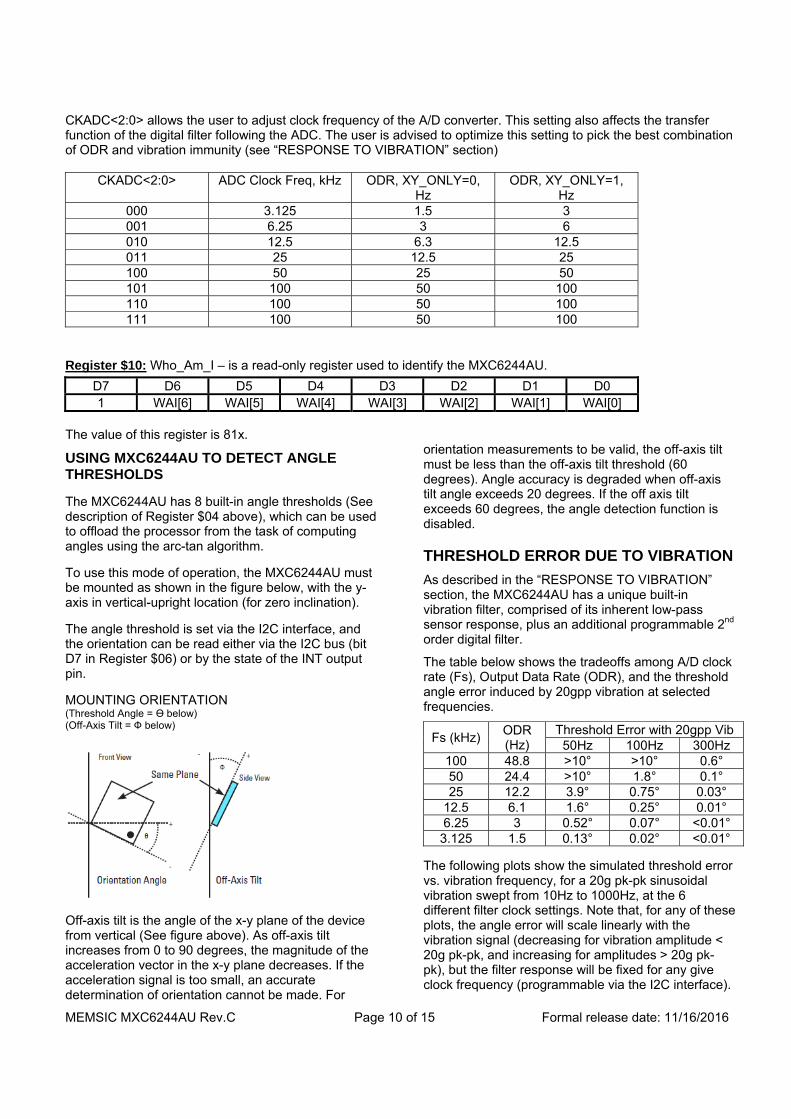
CKADC<2:0> allows the user to adjust clock frequency of the A/D converter. This setting also affects the transfer function of the digital filter following the ADC. The user is advised to optimize this setting to pick the best combination of ODR and vibration immunity (see “RESPONSE TO VIBRATION” section)
CKADC<2:0> ADC Clock Freq, kHz ODR, XY_ONLY=0, Hz
ODR, XY_ONLY=1, Hz
000 3.125 1.5 3 001 6.25 3 6 010 12.5 6.3 12.5 011 25 12.5 25 100 50 25 50 101 100 50 100 110 100 50 100 111 100 50 100
Register $10: Who_Am_I – is a read-only register used to identify the MXC6244AU.
D7 D6 D5 D4 D3 D2 D1 D0 1 WAI[6] WAI[5] WAI[4] WAI[3] WAI[2] WAI[1] WAI[0]
The value of this register is 81x.
USING MXC6244AU TO DETECT ANGLE THRESHOLDS
The MXC6244AU has 8 built-in angle thresholds (See description of Register $04 above), which can be used to offload the processor from the task of computing angles using the arc-tan algorithm.
To use this mode of operation, the MXC6244AU must be mounted as shown in the figure below, with the y-axis in vertical-upright location (for zero inclination).
The angle threshold is set via the I2C interface, and the orientation can be read either via the I2C bus (bit D7 in Register $06) or by the state of the INT output pin.
MOUNTING ORIENTATION (Threshold Angle = ϴ below) (Off-Axis Tilt = Ф below)
Off-axis tilt is the angle of the x-y plane of the device from vertical (See figure above). As off-axis tilt increases from 0 to 90 degrees, the magnitude of the acceleration vector in the x-y plane decreases. If the acceleration signal is too small, an accurate determination of orientation cannot be made. For
orientation measurements to be valid, the off-axis tilt must be less than the off-axis tilt threshold (60 degrees). Angle accuracy is degraded when off-axis tilt angle exceeds 20 degrees. If the off axis tilt exceeds 60 degrees, the angle detection function is disabled.
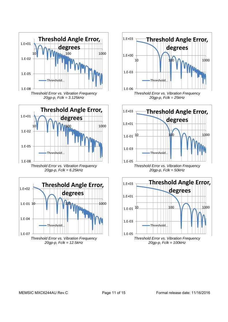
THRESHOLD ERROR DUE TO VIBRATION
As described in the “RESPONSE TO VIBRATION” section, the MXC6244AU has a unique built-in vibration filter, comprised of its inherent low-pass sensor response, plus an additional programmable 2nd order digital filter.
The table below shows the tradeoffs among A/D clock rate (Fs), Output Data Rate (ODR), and the threshold angle error induced by 20gpp vibration at selected frequencies.
Fs (kHz)ODR (Hz)
Threshold Error with 20gpp Vib50Hz 100Hz 300Hz
100 48.8 >10° >10° 0.6° 50 24.4 >10° 1.8° 0.1° 25 12.2 3.9° 0.75° 0.03°
12.5 6.1 1.6° 0.25° 0.01° 6.25 3 0.52° 0.07° <0.01° 3.125 1.5 0.13° 0.02° <0.01°
The following plots show the simulated threshold error vs. vibration frequency, for a 20g pk-pk sinusoidal vibration swept from 10Hz to 1000Hz, at the 6 different filter clock settings. Note that, for any of these plots, the angle error will scale linearly with the vibration signal (decreasing for vibration amplitude < 20g pk-pk, and increasing for amplitudes > 20g pk-pk), but the filter response will be fixed for any give clock frequency (programmable via the I2C interface).
MEMSIC MXC6244AU Rev.C Page 11 of 15 Formal release date: 11/16/2016
Threshold Error vs. Vibration Frequency
20gp-p, Fclk = 3.125kHz
Threshold Error vs. Vibration Frequency
20gp-p, Fclk = 6.25kHz
Threshold Error vs. Vibration Frequency
20gp-p, Fclk = 12.5kHz
Threshold Error vs. Vibration Frequency
20gp-p, Fclk = 25kHz
Threshold Error vs. Vibration Frequency
20gp-p, Fclk = 50kHz
Threshold Error vs. Vibration Frequency
20gp-p, Fclk = 100kHz
1.E‐08
1.E‐05
1.E‐02
1.E+01
10 100 1000
Threshold Angle Error, degrees
Threshold…
1.E‐08
1.E‐05
1.E‐02
1.E+01
10 100 1000
Threshold Angle Error, degrees
Threshold…
1.E‐07
1.E‐04
1.E‐01
1.E+02
10 100 1000
Threshold Angle Error, degrees
Threshold…
1.E‐06
1.E‐03
1.E+00
1.E+03
10 100 1000
Threshold Angle Error, degrees
Threshold…
1.E‐05
1.E‐03
1.E‐01
1.E+01
1.E+03
10 100 1000
Threshold Angle Error, degrees
Threshold…
1.E‐05
1.E‐03
1.E‐01
1.E+01
1.E+03
10 100 1000
Threshold Angle Error, degrees
Threshold…

MEMSIC MXC6244AU Rev.C Page 12 of 15 Formal release date: 11/16/2016
INTERNAL FAULT DETECTION
The MXC6244AU has a variety of internal fault detection circuit features, which can be enabled or disabled via the I2C interface.
On power up (within 10ms of a valid supply voltage appearing on the VDD pin), the internal circuitry checks for the following conditions:
(a) Valid non-volatile memory contents. On power up a CRC algorithm checks if any of the bits have changed from their factory programmed values. If this check is completed successfully the CRC_OK bit is set in the Status register. If this test fails, the output INT will go to a high impedance state until the power supply is removed, or the part is reset via the I2C interface. Note this CRC check cannot be disabled by the user.
In addition to the above test done at power up, the following monitoring is performed on a continuous basis:
(b) If at any time either the X or Y output exceeds 2g continuously for more than approximately 4 seconds (see Note 10), the output is set to a high impedance state, and remains there for as long as the condition persists, or the part is reset by via the I2C interface.
(c) If at any time both the X and the Y outputs fall below 0.375g (which is an indication of either a free fall event, excessive off-axis tilt, or a leak in the gas cavity), the angle-detection function is disabled immediately, to prevent false triggering of the angle comparator. If the condition persists for more than approximately 4 seconds (See Note 10), the output will go to a high impedance state for as long as the condition persists, or the part is reset via the I2C interface.
In each of the above cases (b) and (c), the fault detection circuitry takes precedence over the tip-over detection circuitry (the output will remain in the high impedance state regardless of the angle detected, for as long as the fault condition persists).
Every time the internal failure is detected the FAIL flag will be set in the I2C Status register. The user may choose not to detect the high impedance state of the INT pin, but instead read the Status register on a regular basis. The user may choose to disable checks (b) and (c) by setting I2C bit Dis_Fail in the Detection register.
Finally, there is an additional “Signal Path Self Test” which is available on demand. This self test mode is initiated via the I2C interface (See the section titled “Initiating On-Demand Signal Path Self-Test”. If the self-test bit is enabled, the power is reduced to one of
the heater elements, inducing a deliberate offset in both the X and Y axes of the sensor structure. This offset can be seen on the X and Y digital outputs (via I2C interface), serving as a reliable measure of proper sensor and circuit operation. See the section “Initiating On-Demand Signal Path Self Test” for more details. Note, in this on-demand self-test mode, the angle detection circuitry remains active, so that the application can detect an “artificial” tip-over event.
Note 10: The actual delay time for the triggering of the fault condition (high impedance output) can vary from a minimum of 2.3 sec to a maximum of 5.7 seconds, depending on the state of the internal signal processing when the fault condition is first detected.
SELF-TEST DETAILED DESCRIPTION- INITIATING ON-DEMAND SIGNAL PATH SELF-TEST
As described in the earlier section titled “INTERNAL FAULT DETECTION,” there are 3 different types of fault-detection features built into the MXC6244AU. The first type are done automatically whenever power is first applied, the second type are done continuously in the background during normal operation, and the third type is performed on-demand by a command issued over the I2C interface. This section describes this third type in more detail.
The basic principle of the on-demand self-test is to reduce power to one of the four internal heater elements, inducing a gross offset error, equivalent to approximately +2g on the X channel, and -2g on the Y channel. These offsets can be read via the X and Y I2C registers (see the following section “I2C REGISTER DEFINITION” for a complete description). In this way the sensor and the signal processing electronics can be checked for functionality. In addition, these offsets should cause the INT output to change state for any programmed angle threshold.
An on-demand self-test is executed by the following 6-step procedure:
Step 1: Disable Temperature Compensation (Set the control register bit TempCompDis=1). This step is necessary because the internal temperature compensation function interferes with the self test results.
Step 2: Read the X and Y acceleration values (call them OUTX1 and OUTY1).
Step 3: Enable Self-Test (Set the control bit ST=1), while leaving Temperature Compensation disabled (TempCompDis=1)
Step 4: Wait approximately tbd ms for the X and Y sensor channels to settle, then read the X and Y acceleration values (call them OUTX2 and OUTY2)
Step 5: Subtract OUTX1 from OUTX2 and OUTY1 from OUTY2. These values are the X and Y self-test amplitudes. A dramatic shift (>100mg) in either the X or Y self-test
MEMSIC MXC6244AU Rev.C Page 13 of 15 Formal release date: 11/16/2016
amplitudes over time indicates a fault in the sensor or signal processing electronics
Step 6: Return the device to normal operation (set TempCompDis=0 and ST=0)
Using the above method, the presence of a real constant acceleration stimulus does not affect the ST amplitude, provided that (a) the acceleration plus self-test signal is not so large that the signal path is saturated, and (b) the external acceleration does not change dramatically over the self-test period.
SENSITIVITY TEMPERATURE COMPENSATION
Thermal accelerometers exhibit significant change of sensitivity with temperature. The MXC6244AU includes internal compensation circuitry. Sensitivity change vs. temperature graph for 4 typical devices is shown in the graph.
MEMSIC MXC6244AU Rev.C Page 14 of 15 Formal release date: 11/16/2016
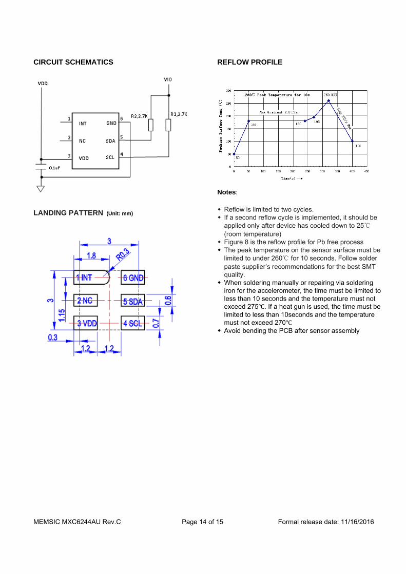
CIRCUIT SCHEMATICS
LANDING PATTERN (Unit: mm)
REFLOW PROFILE
Notes:
Reflow is limited to two cycles. If a second reflow cycle is implemented, it should be
applied only after device has cooled down to 25℃ (room temperature)
Figure 8 is the reflow profile for Pb free process The peak temperature on the sensor surface must be
limited to under 260℃ for 10 seconds. Follow solder paste supplier’s recommendations for the best SMT quality.
When soldering manually or repairing via soldering iron for the accelerometer, the time must be limited to less than 10 seconds and the temperature must not exceed 275 . If a heat gun is used, the time must be limited to less than 10seconds and the temperature must not exceed 270
Avoid bending the PCB after sensor assembly
MEMSIC MXC6244AU Rev.C Page 15 of 15 Formal release date: 11/16/2016
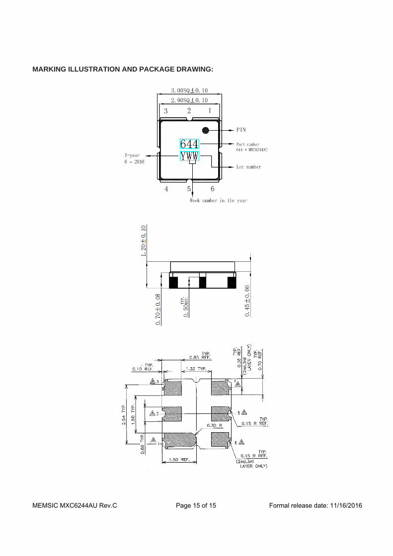
MARKING ILLUSTRATION AND PACKAGE DRAWING: