82558 fast ethernet pci bus controller with integrated phy
TRANSCRIPT

82558 Fast Ethernet PCI Bus Controller with Integrated PHYNetworking Silicon
Datasheet
Product Features
Provides IEEE 802.3/802.3u 10BASE-T and 100BASE-TX compatibility
Provides glueless 32-bit PCI bus master interface
Contains internal 3 Kbyte transmit and 3 Kbyte receive FIFOs
Allows fast back-to-back transmit at 100 Mbps within minimum Interframe Spacing (IFS)
Provides up to 64 Kbyte Flash support for LANDesk® Service Agent® and other supported option ROMs
Supports EEPROM configuration and customized feature selection
Complies with Advanced Configuration and Power Interface (ACPI) Specification, Revision 1.0, PCI Power Management Specification, Revision 1.0, and Advanced Power Management (APM) Specification, Revision 1.2
Supports remote wake-up (Magic Packet*) in APM and ACPI modes
Provides ACPI “interesting” packet wake-up support in D0 to D3cold low power states
Integrates 100BASE-TX Physical Layer (PHY) interface and 10BASE-T serial Encoder/Decoder (ENDEC) and transceiver with built-in transmit and receive filters
Supports IEEE 802.3u Auto-Negotiation for 100BASE-TX and 10BASE-T
Allows full or half duplex support at 10 or 100 Mbps
Supports IEEE 802.3x flow control Supports Bay Technologies flow control Supports three LEDs Maintains streamlined 82557-style chained
memory structure for superior performance Maintains backward software compatibility
to the 82557 Fast Ethernet Controller 5 volt part 208-pin Shrink Quad Flat Package (SQFP)
Figure 1. 82558 Simplified Block Diagram
100Base-TX10Base-T
PHY
10/100 MbpsCSMA/CD
3 KbyteTX FIFO
3 KbyteRX FIFO
FIFOControl
Micro-machine
DualPortedFIFO
PCI Target andFlash/EEPROM/MDI
Interface
Four ChannelAddressing Unit -
DMA
PCI BusInterface Unit -
BIU
Data InterfaceUnit - DIU
TP
EIn
terf
ace
MII Interface
Loca
l Mem
ory
Inte
rfac
eP
CI I
nte
rfa
ce
Order Number: 679016-004Revision 2.3
January 1998

82558
2
Information in thisproperty rights is gwhatsoever, and Infitness for a particintended for use in
Intel may make ch
Designers must nofuture definition an
The 82558 Fast Eto deviate from pu
Contact your local
Copies of docume
Copyright © Intel C
*Third-party brand
Datasheet
document is provided in connection with Intel products. No license, express or implied, by estoppel or otherwise, to any intellectual ranted by this document. Except as provided in Intel's Terms and Conditions of Sale for such products, Intel assumes no liability tel disclaims any express or implied warranty, relating to sale and/or use of Intel products including liability or warranties relating to
ular purpose, merchantability, or infringement of any patent, copyright or other intellectual property right. Intel products are not medical, life saving, or life sustaining applications.
anges to specifications and product descriptions at any time, without notice.
t rely on the absence or characteristics of any features or instructions marked "reserved" or "undefined." Intel reserves these for d shall have no responsibility whatsoever for conflicts or incompatibilities arising from future changes to them.
thernet PCI Bus Controller with Integrated PHY may contain design defects or errors known as errata which may cause the product blished specifications. Current characterized errata are available on request.
Intel sales office or your distributor to obtain the latest specifications and before placing your product order.
nts which have an ordering number and are referenced in this document, or other Intel literature, may be obtained from:
Intel Corporation P.O. Box 7641 Mt. Prospect IL 60056-7641
or call 1-800-879-4683.
orporation, 1997
s and names are the property of their respective owners.

82558
Contents
1.0 Introduction................................................................................................................ .......51.1 82558 Overview ................................................................................................. 51.2 Compliance with Industry Standards ................................................................. 5
2.0 82558 Architecture Overview ..........................................................................................7
2.1 Parallel Subsystem Overview ............................................................................ 72.2 FIFO Subsystem Overview ................................................................................ 82.3 10/100 Mbps CSMA/CD Unit Overview ............................................................. 82.4 100BASE-TX/10BASE-T Physical Layer Interface Unit Overview..................... 9
3.0 Device Pinout ............................................................................................................... ...11
3.1 Pin Identification............................................................................................... 113.2 Signal Type Definition ..................................................................................... 123.3 PCI Bus Interface Signals ................................................................................ 13
3.3.1 PCI Address and Data Pins ............................................................... 133.3.2 PCI Interface Control Pins ................................................................. 143.3.3 PCI Error Reporting Pins ................................................................... 143.3.4 PCI Interrupt Pins ............................................................................... 143.3.5 PCI Arbitration Pins ............................................................................ 153.3.6 PCI System Pins ................................................................................ 15
3.4 Local Memory Interface Pins .......................................................................... 153.5 Clock Pins ....................................................................................................... 163.6 TPE Pins ......................................................................................................... 173.7 LED Pins ......................................................................................................... 173.8 External Bias Pins ........................................................................................... 173.9 Miscellaneous Control of Operation ................................................................ 173.10 Power and Ground .......................................................................................... 183.11 Reserved ......................................................................................................... 193.12 No Connection ................................................................................................ 19
4.0 Hardware Interface .........................................................................................................2 1
4.1 PCI Bus Interface............................................................................................. 214.1.1 PCI Configuration Space .................................................................... 214.1.2 82558 Bus Operations ........................................................................ 284.1.3 Memory Write and Invalidate .............................................................. 354.1.4 Read Align .......................................................................................... 35
4.2 Flash/EEPROM Interface................................................................................. 364.2.1 Flash Interface .................................................................................... 364.2.2 EEPROM Interface ............................................................................. 37
4.3 10/100 Mbps CSMA/CD Unit ........................................................................... 394.3.1 Full Duplex .......................................................................................... 394.3.2 Flow Control........................................................................................ 404.3.3 Address Filtering Modifications ........................................................... 404.3.4 VLAN Support ..................................................................................... 40
4.4 Media Independent Interface (MII) Management Interface.............................. 414.4.1 Management Data Interface (MDI) Register ....................................... 41
4.5 100BASE-TX PHY Unit.................................................................................... 414.5.1 100BASE-TX Transmit Clock Generation........................................... 414.5.2 100BASE-TX Transmit Blocks ............................................................ 424.5.3 100BASE-TX Receive Blocks ............................................................. 45
Datasheet 3

82558
Contents
4.5.4 100BASE-TX Collision Detection........................................................ 464.5.5 100BASE-TX Link Integrity and Auto-Negotiation Solution ................ 464.5.6 Auto 10/100 Mbps Speed Selection ................................................... 464.6 10BASE-T Functionality................................................................................... 474.6.1 10BASE-T Transmit Clock Generation ............................................... 474.6.2 10BASE-T Transmit Blocks ................................................................ 474.6.3 10BASE-T Receive Blocks ................................................................. 474.6.4 10BASE-T Collision Detection ............................................................ 484.6.5 10BASE-T Link Integrity ..................................................................... 484.6.6 10BASE-T Jabber Control Function.................................................... 484.6.7 10BASE-T Full Duplex ........................................................................ 48
4.7 Management Data Interface (MDI) Register Set ............................................. 494.7.1 MDI Registers 0 - 7 ............................................................................. 494.7.2 MDI Registers 8 - 15........................................................................... 524.7.3 MDI Register 16 - 31........................................................................... 52
4.8 Auto-Negotiation Functionality......................................................................... 554.8.1 Overview............................................................................................. 554.8.2 Description .......................................................................................... 554.8.3 Parallel Detect and Auto-Negotiation.................................................. 56
4.9 LED Description............................................................................................... 574.10 Power Management......................................................................................... 57
4.10.1 Wake-up Packet ................................................................................. 584.10.2 Wake on LAN* (WOL) Mode............................................................... 584.10.3 Low Power Mode Requirements......................................................... 594.10.4 82558 Device Power States ............................................................... 604.10.5 Link Operation .................................................................................... 614.10.6 Power Management Registers............................................................ 614.10.7 Power Management Feature Enhancements for the 82558 B-step.... 64
5.0 Software Interface .......................................................................................................... 71
5.1 The Shared Memory Communication Architecture.......................................... 715.2 Initializing the 82558 ........................................................................................ 725.3 Controlling the 82558....................................................................................... 72
5.3.1 The 82558 Control and Status Register ............................................. 73
6.0 Electrical Specifications and Timings .......................................................................... 77
6.1 Absolute Maximum Ratings ............................................................................. 776.2 DC Specifications ............................................................................................ 776.3 AC Specifications............................................................................................. 80
6.3.1 PCI Interface....................................................................................... 806.4 Timing Specification......................................................................................... 81
6.4.1 Clock Specifications............................................................................ 816.4.2 Timing Parameters ............................................................................. 82
7.0 Physical Attributes and Dimensions ............................................................................ 87
8.0 Revision History ........................................................................................................... . 89
4 Datasheet

82558
. Its
2557 t are
rly Write
ther
e CPU le
ork lso
ode
port
etwork EE
ass
1.0 Introduction
1.1 82558 Overview
The 82558 is Intel's first fully integrated 10BASE-T/100BASE-TX LAN solution. It consists ofboth the Media Access Controller (MAC) and the 10/100 Mbps Physical Layer (PHY) interfacebasic functionality is equivalent to that of two of Intel’s previous generation components: the 8Ethernet controller and the 82555 physical layer interface device. Enhancements include, bunot limited to: Advanced Configurations and Power Interface (ACPI) and Advanced Power Management (APM), system manageability support via byte wide management interface, eareceive interrupt support in hardware, and increased PCI command support for the Memory and Invalidate (MWI) command.
As a controller, the 82558 is a sophisticated 32-bit PCI component, with enhanced scatter-gabus mastering capabilities. Its true 32-bit architecture enables it to perform high speed data transfers on the PCI bus using four DMA channels. Its sophisticated microcode-based enginenables the 82558 to process high level commands and perform multiple operations withoutintervention. Its 3 Kbyte Transmit and Receive FIFOs provide large on-chip storage of multiptransmit and receive frames.
The 82558 physical media interface module (PHY unit) enables direct connection to the netwmedia. It provides full support for both 100BASE-TX and 10BASE-T operation. The 82558 aprovides the NWay* Auto-Negotiation capability that enables it to detect speed and duplex (mof operation) automatically.
The 82558 provides full support for both half duplex and full duplex operation, as well as supfor full duplex flow control.
1.2 Compliance with Industry Standards
The 82558 has two primary interfaces. The host system PCI bus interface and the serial or ninterface. The network interface complies to the IEEE 802.3 for 10BASE-T and TX and the IE802.3u for 100BASE-T and TX Ethernet interfaces. The 82558 also complies to the PCI BusSpecification, Revision 2.1; PCI Power Management Interface Specification, Revision 1.0; Advanced Configuration and Power Interface Specification, Revision 1.0; Network Device ClPower Management Specification, Revision 1.0.
Datasheet 5

82558
6 Datasheet

82558
four nd a
a PCI d a , eters
to a
ol sses
ee ceive or
used tained
ment
ine
ne ne ss to Unit is ce of s and
de
ddress the oot
2.0 82558 Architecture Overview
Figure 1 (on the cover page) shows a high level block diagram of the 82558. It is divided intomain subsystems: a parallel subsystem, a FIFO subsystem, a 10/100 Mbps CSMA/CD unit a10/100 PHY unit.
2.1 Parallel Subsystem Overview
The parallel subsystem is divided into several functional blocks: a PCI Bus Master Interface, Bus Slave block, a Micromachine processing unit and its corresponding microcode ROM, anFlash and EEPROM interface. The parallel subsystem also interfaces to the FIFO subsystempassing data (such as transmit, receive and configuration data), command, and status parambetween these two blocks.
The PCI Bus Master Interface provides a complete interface to a PCI bus and is compliant toRevision 2.1 of the PCI Bus Specification. No external logic is required to interface the 82558PCI bus. The 82558 provides 32 pins for addressing and data, as well as the complete contrinterface to operate on a PCI bus. It follows the PCI Configuration format which allows all acceto the 82558 (control register, Flash accesses, Boot, etc.) to be automatically mapped into frmemory and I/O space upon initialization of a PCI system. For processing of transmit and reframes, the 82558 operates as a master on the PCI bus, initiating Zero Wait State transfers ftransporting network traffic. Section 4.1, “PCI Bus Interface” on page 21 provides more details on the operation of the 82558 PCI interface.
The PCI Target block consists of registers which either directly control the 82558 or which areto interface other devices through the 82558. The 82558 Control/Status Register Block is conas part of these elements. The Control/Status Register Block consists of the following 82558internal control registers: SCB, PORT, Flash control register, EEPROM control register, MDIControl register, Early Receive Interrupt register, Flow Control registers, and Power Manageregister.
The Micromachine is an embedded processing unit contained in the 82558. The Micromachaccesses the 82558 microcode ROM working its way through the opcodes (or instructions) contained in the ROM to perform its functions. Parameters accessed from memory such as Transmit Buffer Descriptor fields or pointers to data buffers are also used by the Micromachiduring processing of RCV or XMT frames by the 82558. A typical function of the Micromachiwould be to take a data buffer pointer field, and load it into the 82558 DMA unit for direct accethe data buffer. The Micromachine is divided into two units, a Receive Unit and a Command (including XMT functions). These two units operate independently and concurrently. Control switched between the two units according to the microcode instruction flow. The independenthe Receive and Command units of the Micromachine allow the 82558 to execute commandreceive incoming frames simultaneously.
The Micromachine also has a RAM memory which can be loaded with additional microcode instructions which modify the operation of the 82558. This ability enables the 82558 to proviAdaptive Technology flexibility which can tailor 82558 behavior to various operating environments.
The 82558 contains an interface to both an external Flash memory, and an external serial EEPROM. The Flash interface, which could also be used to connect to any standard 8-bit EEPROM device, provides up to 64 Kbyte of addressing to the Flash. It uses a multiplexed ascheme which works in conjunction with an LS373 circuit, or compatible latch to de-multiplexaddress. Both Read and Write accesses are supported. The Flash may be used for remote b
Datasheet 7
82558
ystem o
l e erface
h rface llows
ssion
ut
inate
82558 posed
558 he
e ta to
et MII SMA/ of the
an on of
ta ide
tains and
functions, network statistical and diagnostics functions, etc. The Flash is mapped into host smemory (anywhere within the 32-bit memory address space) for software accesses. It is alsmapped into an available boot expansion ROM location during boot time of the system. Moreinformation on the Flash interface is provided in Section 4.2.1, “Flash Interface” on page 36. The EEPROM is used to store relevant information for a LAN connection such as Node IndividuaAddress, as well as board manufacturing and configuration information. Both Read and Writaccesses to the EEPROM are supported by the 82558. More information on the EEPROM intis provided in Section 4.2.2, “EEPROM Interface” on page 37.
2.2 FIFO Subsystem Overview
The 82558 FIFO subsystem consists of a 3 Kbyte XMT FIFO and a 3 Kbyte RCV FIFO. EacFIFO is unidirectional, and independent of the other. The FIFO subsystem serves as the intebetween the 82558 parallel side and the serial CSMA/CD unit. It provides a temporary bufferstorage area for frames as they are either being received or transmitted by the 82558. This afor several important features in the 82558:
• Transmit frames can be queued within the Transmit FIFO, allowing back-to-back transmiwithin minimum interframe spacing (960 nanoseconds at 100 Mbps operation).
• The storage area in the FIFO allows the 82558 to withstand long PCI bus latencies witholosing incoming data or corrupting outgoing data.
• The 82558 Transmit FIFO threshold allows the transmit start threshold to be tuned to elimunderruns while concurrent transmits are being performed.
• The FIFO subsection allows extended PCI zero wait state burst accesses to or from the for both receive and transmit frames, since the transfer is to the FIFO storage area as opto directly to the serial link.
• Erred transmissions (COL, Congestion, Underrun) are retransmitted directly from the 82FIFO, increasing performance and eliminating the need to retrieve this data again from thost system.
• Incoming Runt Receive Frames (in other words, frames less than the legal minimum framsize) can be discarded automatically by the 82558 without transferring this erroneous dathe host system.
2.3 10/100 Mbps CSMA/CD Unit Overview
The CSMA/CD unit of the 82558 allows it to be connected to either a 10 or 100 Mbps Ethernnetwork. The 82558 CSMA/CD unit interfaces to either an external IEEE 802.3 10/100 Mbpscompatible PHY device or directly to the internal 10/100 Mbps PHY unit. In both cases the CCD unit can switch automatically between 10 or 100 Mbps operation depending on the speednetwork. The CSMA/CD unit performs all the functions of the 802.3 protocol such as frame formatting, frame stripping, collision handling, deferral to link traffic, etc. The CSMA/CD unit calso be placed in a full duplex mode which allows for simultaneous transmission and receptiframes.
The CSMA/CD unit accepts data from the 82558 XMT FIFO and converts it to nibble-wide dafor transmission on the link. During reception, the CSMA/CD unit converts data from nibble-wto a byte-wide format and transfers it to the RCV FIFO of the 82558. The CSMA/CD unit cona Management Data Interface to an MII compliant PHY. This allows software to pass controlstatus parameters between the 82558 MAC and PHY in a consistent manner.
8 Datasheet

82558
er
s
into
alog ling, ce to
used
.
2.4 100BASE-TX/10BASE-T Physical Layer Interface Unit Overview
The internal architecture of the PHY Unit is a combination of advanced DSP, analog, and othfunctional blocks.
In 100BASE-TX mode, the analog subsection of the PHY Unit performs two functions: it takereceived analog MLT-3 data from the RD pair, converts it into a digital 125 Mbps stream, recovering both clock and data. The second function is to convert a digital 125 Mbps streamMLT-3 format and drive it through the TD pair into the physical medium.
In 100BASE-TX mode, the digital subsection performs all necessary signal processing of thedigital data obtained from the analog reception and of the data that will be driven into the antransmit subsection. This includes 4B/5B encoding and decoding, scrambling and descrambcarrier sense, collision detection, link detection, auto-negotiation and providing an MII interfathe CSMA/CD unit.
The PHY Unit operation in 10BASE-T mode is similar. Manchester encoding and decoding isinstead of scrambling/descrambling and 4B/5B encoding/decoding, and the internal TXCLK/RXCLK MII clocks provide 2.5 MHz instead of 25 MHz to the CSMA/CD unit.
Figure 1 shows a diagram of the internal PHY Unit and how it connects to an RJ45 connector
Figure 1. PHY Unit Block Diagram
4b/5bEncoding
Scram bler
Serialization
M II TX In terface
NR Z to NR ZI
NR ZI to M LT3
4b/5bDecoding
De-scram bler
Serial to 5B
M II R X In terface
NR ZI to NR Z
M LT3 to N RZI
M agnetics M odule
RJ-45 C onnector
1 2 3 6
Datasheet 9

82558
10 Datasheet

82558
re
3.0 Device Pinout
3.1 Pin Identification
Figure 2 shows the name, number, and location of each pin on the device. Pin descriptions aprovided in the sections that follow.
Figure 2. Intel 82558 Pin Identification Diagram
F L D 4
F L D 2 E E D I
F L D 1 E E D O
V S S
F L D 7
F L D 6
F L D 5
A D 0
V S S
A D 1
V S S
A D 5
V S S
A D 6
A D 7
A D 4
A D 3
A D 2
C B E # 0
A D 8
AD
9
V C C
V C C
AD
14
CB
E#
1
AD
15
PA
R
ST
OP
#
DE
VS
EL
#
TR
DY
#
CB
E#
2
IRD
Y#
FR
AM
E#
AD
16
AD
20
AD
21
AD
22
AD
23
CB
E#
3
AD
24
AD
25
AD
19
AD
18
AD
17
VC
C
AD
13
IDS
EL
AD
26
AD
27
SL
VT
RI
LIS
TA
T/A
UX
VS
SA
VC
CA
VS
S
VC
C
V C C
V S S
Intel 82558(B-step)
(Top View)
© 1997 Intel Corporat ion.Al l r ights reserved.
2 6
2 5
2 4
2 3
2 2
2 1
2 0
1 9
1 8
1 7
1 6
1 5
1 4
1 3
1 2
1 1
1 0
9
8
7
6
5
4
3
2
1
5 2
5 1
5 0
4 9
4 8
4 7
4 6
4 5
4 4
4 3
4 2
4 1
4 0
3 9
3 8
3 7
3 6
3 5
3 4
3 3
3 2
3 1
3 0
2 9
2 8
2 7
78
77
76
75
74
73
72
71
70
69
68
67
66
65
64
63
62
61
60
59
58
57
56
55
54
53
10
4
10
3
10
2
10
1
10
0
99
98
97
96
95
94
93
92
91
90
89
88
87
86
85
84
83
82
81
80
79
1 0 5
1 0 6
1 0 7
1 0 8
1 0 9
1 1 0
1 1 1
1 1 2
1 1 3
1 1 4
1 1 5
1 1 6
1 1 7
1 1 8
1 1 9
1 2 0
1 2 1
1 2 2
1 2 3
1 2 4
1 2 5
1 2 6
1 2 7
1 2 8
1 2 9
1 3 0
1 3 1
1 3 2
1 3 3
1 3 4
1 3 5
1 3 6
1 3 7
1 3 8
1 3 9
1 4 0
1 4 1
1 4 2
1 4 3
1 4 4
1 4 5
1 4 6
1 4 7
1 4 8
1 4 9
1 5 0
1 5 1
1 5 2
1 5 3
1 5 4
1 5 5
1 5 6
18
3
18
4
18
5
18
6
18
7
18
8
18
9
19
0
19
1
19
2
19
3
19
4
19
5
19
6
19
7
19
8
19
9
20
0
20
1
20
2
20
3
20
4
20
5
20
6
20
7
20
8
15
7
15
8
15
9
16
0
16
1
16
2
16
3
16
4
16
5
16
6
16
7
16
8
16
9
17
0
17
1
17
2
17
3
17
4
17
5
17
6
17
7
17
8
17
9
18
0
18
1
18
2
VS
S
VS
SA
TD
N
VC
CA
TD
P
VC
CA
RD
N
VR
EF
VS
SA
RB
IAS
10
0
RB
IAS
10
RD
P
VS
SA
VC
CA
VS
SA
VC
CA
VS
SA
VC
CA
VS
SA
VS
S
LIL
ED
AC
TL
ED
SP
EE
DL
ED
VS
SA
VC
CA
VS
S
VS
SA
VC
CA
X2
X1
V S S
R S V D
R S V D
Z R E F
V S S
R S V D
R S V D
R S V D
R S V D
R S V D
R S V D
R S V D
R S V D
A D 2 8
A D 2 9
A D 3 0
A D 3 1
R E Q #
G N T #
R S T #
INTA#
V C C
T E S T
V C C
V S S
V C C
V S S
F L A D D R 3
F L A D D R 2
F L A D D R 1
F L A D D R 0
F L A D D R 7
F L A D D R 5
F L A D D R 4
V C C
F L W E #
F L O E #
F L C S #
V S S
A L T R S T #
I S O L A T E #
V S S
P M E #
V S S
V S S
F L D 3
V S S
V S S
F L A D D R 6
V C C
V S S
VC
C
AD
10
AD
11
AD
12
VS
S
VS
S
R S V D
R S V D
VS
S
VC
C
VS
S
VS
S
VC
C
VS
S
VS
S
VC
C
VS
S
VS
S
V S S
VS
SA
VS
SA
R S V D
V C C
R S V D
RS
VD
VS
S
VC
C
V S S
V S S
R S V D
R S T O U T
NC
NC
NC
NC
NC
NC
NC
C L K
V S S
V C C
V C C
V S S
V C C
V S S
V C C
V S S
V S S
VS
S
VS
S
VC
C
VS
S
VS
S
PE
RR
#
SE
RR
#
N C
V S S
V C C
V C C
V S S
V S S
V C C
V S S A
V C C A
V S S A
V C C A
FL
D0
EE
SK
EE
CS
VS
S
VC
C
VS
SA
VC
CA
Datasheet 11
82558
3.2 Signal Type Definition
Signal Type Name Definition
IN Input Input is a standard Input-only signal.
OUT Totem Pole Output This is a standard active driver.
I/O Input/Output This is an input/output signal.
T/S Tri-State Tri-state is a bi-directional, tri-state input/output pin.
S/T/S Sustained Tri-State Sustained Tri-State is an active low tri-state signal owned and driven by one agent at a time. The agent that drives an s/t/s pin low must drive it high for at least one clock before letting it float. A new agent cannot start driving a s/t/s signal any sooner than one clock after the previous owner tri-states it.
O/D Open Drain This allows multiple devices to share as a wired-OR.
B Bias This is used as a bias pin.
12 Datasheet
82558
3.3 PCI Bus Interface Signals
3.3.1 PCI Address and Data Pins
Symbol Pin Type Name and Function
AD31
AD30
AD29
AD28
AD27
AD26
AD25
AD24
AD23
AD22
AD21
AD20
AD19
AD18
AD17
AD16
AD15
AD14
AD13
AD12
AD11
AD10
AD9
AD8
AD7
AD6
AD5
AD4
AD3
AD2
AD1
AD0
46
47
51
52
54
55
57
58
63
65
66
69
70
72
73
75
93
94
95
97
99
101
102
105
107
110
112
113
115
116
118
119
T/S Address and Data . The address and data signals, AD[31:0], are multiplexed on the same PCI pins by the 82558. A bus transaction consists of an address phase followed by one or more data phases. The address phase is the clock cycle in which FRAME# is asserted. During the address phase, AD[31:0] contains a physical address (32 bits). For I/O, this is a byte address; for configuration and memory, it is a Dword address. The 82558 uses little endian byte ordering. AD[31:24] contain the most significant byte (MSB) and AD[7:0] contain the least significant byte (LSB).
C/BE3#
C/BE2#
C/BE1#
C/BE0#
62
76
92
106
T/S Command and Byte Enable . The Command/Byte Enable signals are multiplexed on the same PCI pins by the 82558. During the address phase of a transaction, C/BE[3:0]# defines the bus command. During the data phase C/BE[3:0]# are used as Byte Enables. The Byte Enables are valid for the entire data phase and determine which byte lanes carry meaningful data. C/BE[3]# applies to byte 3 (MSB) and C/BE[0]# applies to byte 0 (LSB).
PAR 90 T/S Parity . Parity is even parity across AD[31:0] and C/BE[3:0]#. PAR is stable and valid one clock after the address phase. For data phases, PAR is stable and valid one clock after either IRDY# is asserted during a write transaction or TRDY# is asserted during a read transaction. Once PAR is valid, it remains valid until one clock after the completion of the current data phase. The master drives PAR for address and write data phases; the target drives PAR for read data phases.
Datasheet 13

82558
3.3.2 PCI Interface Control Pins
3.3.3 PCI Error Reporting Pins
3.3.4 PCI Interrupt Pins
Symbol Pin Type Name and Function
FRAME# 78 S/T/S Cycle Frame . Frame# is driven by the 82558 to indicate the beginning and duration of a transaction. Frame# is asserted to indicate a bus transaction is beginning and remains asserted as data transfers continue. FRAME# is de-asserted during the final data phase.
IRDY# 79 S/T/S Initiator Ready . IRDY# is driven by the 82558 as a bus master and indicates the 82558’s ability to complete the current data phase of the transactions. IRDY# is used in conjunction with TRDY#. A data phase is completed on any clock where both IRDY# and TRDY# are asserted. During a write, IRDY# indicates that valid data is present on AD[31:0]. During a read, it indicates that the 82558 is prepared to accept data. Wait cycles are inserted until both IRDY# and TRDY# are asserted together.
TRDY# 83 S/T/S Target Ready . TRDY# is driven by the 82558 as a slave (selected device) and indicates its ability to complete the current data phase of the transaction. TRDY# is used in conjunction with IRDY#. A data phase is completed on any clock where both TRDY# and IRDY# are asserted. During a read, TRDY# indicates that valid data is present on AD[31:0]. During a write, it indicates that the 82558 is prepared to accept data. Wait cycles are inserted until both TRDY# and IRDY# are asserted together.
STOP# 86 S/T/S Stop . STOP# is driven by the target and indicates its request to the master to stop the current transaction. As a slave, STOP# is driven by the 82558 to inform the bus master to stop the current transaction. As a master, STOP# is received by the 82558 and stops the current transaction.
IDSEL 59 IN Initialization Device Select . IDSEL is used by the 82558 as a chip select during configuration read and write transactions.
DEVSEL# 84 S/T/S Device Select . As a master, DEVSEL# is an input to the 82558 indicating whether any device on the bus has been selected. As a slave, the 82558 drives DEVSEL# to indicate that the 82558 has decoded its address as the target of the current transactions. As an input, DEVSEL# indicates whether any device on the bus has been selected.
Symbol Pin Type Name and Function
SERR# 89 O/D System Error . SERR# is used by the 82558 to report address parity errors. SERR# is an open drain signal and is actively driven for one PCI clock when reporting the error.
PERR# 87 S/T/S Parity Error . PERR# is used by the 82558 to report data parity errors during all PCI transactions. The PERR# pin is sustained tri-state. It must be driven active by the 82558 two clocks after the data phase in which a data parity error is detected. The minimum duration of PERR# is one clock for each data phase that a data parity error is detected. An agent cannot report a PERR# until it has claimed the access by asserting DEVSEL# and completed a data phase.
Symbol Pin Type Name and Function
PME# 39 O/D Power Management Event . The PME# signal indicates that a power management event has occurred. This is an active low signal.
PME# should be driven high whenever the TEST pin is asserted.
14 Datasheet

82558
3.3.5 PCI Arbitration Pins
3.3.6 PCI System Pins
3.4 Local Memory Interface Pins
INTA# 42 O/D Interrupt A . INTA# is used to request an interrupt by the 82558. This is an active low level triggered interrupt signal.
Symbol Pin Type Name and Function
REQ# 41 T/S Request . The REQ# signal indicates to the arbiter that the 82558 desires use of the bus. This is a point to point signal. (Every master has its own REQ#.)
GNT# 38 IN Grant . GNT# indicates to the 82558 that access to the bus has been granted. This is a point to point signal. (Every master has its own GNT#.)
Symbol Pin Type Name and Function
CLK 35 IN Clock . The CLK signal provides timing for all transactions on the PCI bus and is an input to every PCI device, including the 82558. All PCI signals, except RST# and INT#, are sampled on the rising edge of CLK. All other timing parameters are defined with respect to this edge.
ISOLATE# 31 IN Isolate . The ISOLATE# signal is used to isolate the 82558 from the PCI bus. ISOLATE# is active low. When asserted, the 82558 does not drive its PCI outputs (excluding PME#) or sample its PCI inputs (including CLK and RST#).
RST# 37 IN Reset . RST# is used to bring PCI-specific registers, sequencers, and signals to an initialized state. Anytime RST# is asserted, all PCI output signals are driven to their benign state. In general, this means they are tri-stated with one exception. The exception is that SERR# (open drain) is floated.
ALTRST# 36 IN Alternate Reset . ALTRST# is used to reset the 82558 when the PCI RST# pin is not available.
Symbol Pin Type Name and Function
EECS 160 OUT EEPROM Chip Select . EECS is an active high signal used to assert chip select to the serial EEPROM.
FLD0/
EESK
159 T/S Flash Data 0/EEPROM Shift Clock . FLD0/EESK is a multiplexed pin. During Flash access, it acts as Flash Data 0 I/O pin. During EEPROM access, it acts as an EEPROM shift clock output to shift data in and out of the serial EEPROM.
FLD1/
EEDO
156 T/S Flash Data 1/EEPROM Data Out . FLD1/EEDO is a multiplexed pin. During Flash access, it acts as Flash Data 1 I/O pin. During EEPROM access, it acts as the input pin for the EEPROM’s data output.
FLD2/
EEDI
155 T/S Flash Data 2/EEPROM Data In . FLD2/EEDI is a multiplexed pin. During Flash access, it acts as the Flash Data 2 I/O pin. During EEPROM access, it acts as the output pin for the EEPROM’s data input.
Symbol Pin Type Name and Function
Datasheet 15
82558
3.5 Clock Pins
FLD7
FLD6
FLD5
FLD4
FLD3
144
146
151
153
154
T/S Flash Data . FLD[7:0] signals are used for I/O.
For the A-step only, FLD4 is used as the low power signal in Wake on LAN* mode. When the Remote Wake Up bit is set in the EEPROM and the FLD4 input is high, the 82558 enters low power mode.
FLADDR7
FLADDR6
FLADDR5
FLADDR4
FLADDR3
FLADDR2
FLADDR1
FLADDR0
128
132
135
136
139
140
142
143
OUT Flash Address . FLADDR[7:0] work in conjunction with an external 8-bit address latch to control Flash addressing up to 64 Kbyte. The 8 Flash Address pins should be connected to both the address latch and address pins 7 to 0 of the Flash. The address latch provides the upper 8-bits, bits 15 to 8, of address to the Flash and is latched by assertion of the Flash Chip Select (FLCS#) pin.
FLCS# 127 OUT Flash Chip Select . FLCS# will normally be high to disable access to the Flash. When a Flash high address needs to be latched, FLCS# is asserted low. This is how the data is latched and Flash is enabled. FLCS# should be connected to both the enable pin on the external address latch and the chip enable pin on the Flash.
FLOE# 122 OUT Flash Output Enable . FLOE# provides the active low output enable control to the Flash.
FLOE# also operates as the Test Execute (TEXEC) input when the Test pin is asserted. TEXEC is the indication to the 82558 test port to start performing the instruction that has been clocked in on TI.
FLWE# 123 OUT Flash Write Enable . FLWE# provides the active low write enable control to the Flash.
FLWE# operates as the Test Clock (TCK#) input when the Test pin is asserted. TCK# is the Test Clock that clocks test data in the TI pin and out of TOUT.
Symbol Pin Type Name and Function
X1 197 IN Crystal Input One . X1 and X2 can be driven by an external 25 MHz crystal. Otherwise, X1 may be driven by an external MOS level 25 MHz oscillator when X2 is left floating.
X2 198 OUT Crystal Output Two . X1 and X2 can be driven by an external 25 MHz crystal. Otherwise, X1 can be driven by an external MOS level 25 MHz oscillator when X2 is left floating.
Symbol Pin Type Name and Function
16 Datasheet

82558
3.6 TPE Pins
3.7 LED Pins
3.8 External Bias Pins
3.9 Miscellaneous Control of Operation
Symbol Pin Type Name and Function
TDP
TDN
186
187
OUT Transmit Pair. These pins send the serial bit stream for transmission on the UTP cable. The current-driven differential driver can be two level (10BASE-T or Manchester) or three-level (100BASE-TX or MLT-3) signals depending on operating mode. These signals interface directly with an isolation transformer.
RDP
RDN
171
172
IN Receive Pair. These pins receive the serial bit stream from the isolation transformer. The bit stream can be two level (10BASE-T or Manchester) or three-level (100BASE-TX or MLT-3) signals depending on operating mode.
Symbol Pin Type Name and Function
ACTLED# 163 OUT Activity LED. This active-low pin (LED) indicates either transmit or receive activity. When there is activity, ACTLED is on. When there is no activity, ACTLED is off.
LILED# 162 OUT Link Integrity LED. This active-low pin (LED) indicates link integrity. If link is good in either 10 or 100 Mbps the LED is ON, if link is bad the LED is off. In a combo board this LED should be connected to the TX technology LED.
SPEED-LED#
164 OUT Speed LED. This active-low pin (LED) will be on at 100 Mbps and off at 10 Mbps. Note that this LED retains it’s last known state when the link is down.
Symbol Pin Type Name and Function
RBIAS100 182 B Bias Reference Resistor 100. A 634 Ω resistor should be connected from this pin to VSS.
RBIAS10 181 B Bias Reference Resistor 10. A 768 Ω resistor should be connected from this pin to VSS.
VREF 180 B Voltage Reference . VREF is connected to a 2.5 V ± 1% external voltage reference generator. A 220 Ω pull down resistor is used when the internal voltage reference is used.
ZREF 15 B Z Reference . This pin should be pulled up with a 10 KΩ resistor in all applications.
Symbol Pin Type Name and Function
SLVTRI 203 I/O Slave Tri-State . SLVTRI should be driven high when the Test pin is asserted.
LISTAT 204 IN Link Status . LISTAT should be driven high when the Test pin is asserted.
AUX# Auxiliary Power . Pin 204 is used as an auxiliary power indication for the 82558 B-step. Pin 204 pulled low indicates that an auxiliary power supply exists.
Datasheet 17

82558
Note: The shaded area defines the difference in the 82558 B-step from the 82558 A-step.
3.10 Power and Ground
RSTOUT 3 OUT Reset Out . RSTOUT is used when an external PHY is used and is driven high during hardware reset of the 82558.
TEST 30 IN Test . When TEST is high, the 82558 will enable the test port.
Symbol Pin Type Name and Function
VCC 8, 21, 22, 29, 34, 44, 45, 48, 61, 67, 74, 80, 88, 109, 126, 130, 137, 100, 114, 129, 145, 158, 202, 207
VCC VCC Power: +5V ± 5%.
VCCA 147, 149, 166, 167, 169, 174, 176, 178, 183, 193, 195
VCC Analog VCC. +5V ± 5%.
VSS 2, 5, 11, 16, 19, 20, 25, 28, 32, 33, 40, 43, 49, 50, 53,56, 64, 68, 71, 77, 81, 82, 85, 91, 96, 103, 104, 108, 111, 117, 125, 131, 138, 120, 124, 133, 134, 141, 152, 157, 161, 179, 201, 205, 208
VSS VSS. Ground: 0V.
VSSA 148, 150, 165, 168, 170, 173, 175, 177, 184, 185, 188, 189, 192, 194
VSS Analog VSS. Ground: 0V.
Symbol Pin Type Name and Function
18 Datasheet

82558
3.11 Reserved
3.12 No Connection
Symbol Pin Type Name and Function
RSVD 1, 4, 6, 7, 9, 10, 12, 13, 14, 17, 18, 23, 24, 26, 27, 206
Reserved.
Symbol Pin Type Name and Function
NC 60, 98, 121, 190, 191, 196, 199, 200
No connection.
Datasheet 19

82558
20 Datasheet

82558
82558 ).
cts with e, some -chip
allow it
uch as ns
vision
ader
4.0 Hardware Interface
4.1 PCI Bus Interface
The PCI bus interface enables the 82558 to interact with the host system via the PCI bus. It provides the control, address, and data interface for the 82558 to work with a PCI compliantsystem. The PCI bus interface also provides the means for configuring PCI parameters in the(refer to the PCI Bus Interface Specification, Revision 2.1, for more details specific to the PCI bus
The 82558 acts as both a master and a slave on the PCI bus. As a master, the 82558 interathe system main memory to access data for transmission or deposit received data. As a slav82558 control structures are accessed by the host CPU to read or write information to the onregisters. The CPU also provides the 82558 with the necessary commands and pointers thatto process receive and transmit data.
4.1.1 PCI Configuration Space
The 82558 supports all PCI required registers as well as registers needed for its operation (sBase Address Registers). The purpose of these registers will be described in following sectio(Section 4.1.1.1 through Section 4.1.1.5).
The organization of the configuration space registers as defined in the PCI Specification, Re2.1, is shown below in the figure below.
Note: The 82558 configuration space consists of the 16 Dwords of Type 0 Configuration Space He. This region consists of fields that uniquely identify the 82558 and allow it to be generically
Device ID Vendor ID 00h
Status Command 04h
Class Code Revision ID 08h
BIST Header Type Latency Timer Cache Line Size 0Ch
CSR Memory Mapped Base Address Register 10h
CSR I/O Mapped Base Address Register 14h
Flash Memory Mapped Base Address Register 18h
Reserved Base Address Register 1Ch
Reserved Base Address Register 20h
Reserved Base Address Register 24h
Card Bus CIS Pointer (not supported at this time) 28h
Subsystem ID Subsystem Vendor ID 2Ch
Expansion ROM Base Address Register 30h
Reserved Cap_Ptr 34h
Reserved 38h
Max_Lat Min_Gnt Interrupt Pin Interrupt Line 3Ch
Figure 3. PCI Configuration Registers
Datasheet 21

82558
to
control
ses
the PCI
controlled. (If you are familiar with the 82557, the registers that have changed from the 82557the 82558 are marked in bold type.)
4.1.1.1 PCI Configuration Command Register
The 82558 Command register at word address 04h in the PCI configuration space provides over the 82558 ability to generate and respond to PCI cycles. If a 0h is written to this register, the 82558 is logically disconnected from the PCI bus for all accesses except configuration acces. The format of this register is shown in the figure below.
Note that bits three, five, seven, and nine are set to 0b. The table below describes the bits of Command Register.
Figure 4. PCI Command Register
Reserved
SERR# EnableParity Error ResponseMemory Write and Invalidate EnableBus Master EnableMemory SpaceIO space
0000
1015 0123456789
Table 1. PCI Command Register Bits
Bits Name Description
0 I/O Space This bit controls a device’s response to the I/O space accesses. A value of 0b disables the device response. A value of 1b allows the device to respond to I/O space accesses. In the 82558, this bit is configurable and has a default value of 0b.
1 Memory Space This bit controls a device’s response to the memory space accesses. A value of 0b disables the device response. A value of 1b allows the device to respond to memory space accesses. In the 82558, this bit is configurable and has a default value of 0b.
2 Bus Master This bit controls a device’s ability to act as a master on the PCI bus. A value of 0b disables the device from generating PCI accesses. A value of 1b allows the device to behave as a bus master. In the 82558, this bit is configurable and has a default value of 0b.
4 Memory Write and Invalidate Enable
This bit controls a device’s ability to use the Memory Write and Invalidate command. A value of 0b disables the device from using the Memory Write and Invalidate Enable command. A value of 1b enables the device to use the Memory Write and Invalidate command. In the 82558, this bit is configurable and has a default value of 0b.
6 Parity Error Control This bit controls a device’s response to parity errors. A value of 0b causes the device to ignore any parity errors that it detects and continue normal operation. A value of 1b causes the device to take normal action when a parity error is detected. This bit must be set to 0b after RST# is asserted. In the 82558, this bit is configurable and has a default value of 0b.
22 Datasheet

82558
ble
he
Status
ly
Note that the 82558 has the ability to enable or disable the Memory Write and Invalidate Enabit.
4.1.1.2 PCI Status Register
The 82558 Status Register is used to record status information for PCI bus related events. Tformat of this register is shown in the figure below.
Note that bits 21, 22, 26, and 27 are set to 0b and bits 20, 23, and 25 are set to 1b. The PCIRegister bits are described in the table below.
8 SERR# Enable This bit controls a device’s ability to enable the SERR# driver. A value of 0b disables the SERR# driver. A value of 1b enables the SERR# driver. This bit must be set to report address parity errors. In the 82558, this bit is configurable and has a default value of 0b.
10-15 Reserved These bits are reserved and should be set to 000000b.
Table 1. PCI Command Register Bits
Bits Name Description
Figure 5. PCI Status Register
0
Detected Pari ty ErrorSignaled System ErrorReceived Master Abor tReceived Target AbortSignaled Target AbortDevsel T imingPari ty Error DetectedFast Back To Back ( target)Capabil i t ies List
Reserved011000 10
31 30 29 28 27 26 25 24 23 22 21 20 19 16
Table 2. PCI Status Register Bits
Bits Name Description
16-19 Reserved These bits are reserved and should be set to 0000b.
20 Capabilities List This bit indicates whether the 82558 implements a list of new capabilities such as PCI Power Management. A value of 0b means that this function does not implement the Capabilities List. If this bit is set to 1b, the Cap_Ptr register provides an offset into the 82558 PCI Configuration Space pointing to the location of the first item in the Capabilities List. This bit is set only if the PM bit in the EEPROM is set.
23 Fast Back-to-Back This bit indicates a device’s ability to accept fast back-to-back transactions when the transactions are not to the same agent. Avalue of 0b disables fast back-to-back ability. A value of 1b enables fast back-to-back ability. In the 82558, this bit is read onand is set to 1b.
Datasheet 23

82558
558
se
Note that bit 20 is the Capabilities List bit and holds a fixed value of 1b to indicate that the 82supports the capabilities list. It is loaded from the EEPROM.
4.1.1.3 Device ID and System ID Registers
Seven fields in the PCI Configuration Registers refer to device identification. The 82558 implements these registers as required. The device identification registers allow generic configuration software to determine what devices are available on the system’s PCI bus. Theregisters are described in the table below.
24 Parity Error Detected This bit indicates whether a parity error is detected. This bit is set to 1b when three conditions are met:
1. The bus agent asserted PERR# itself or observed PERR# asserted.
2. The agent setting the bit acted as the bus master for the operation in which the error occurred.
3. The Parity Error Response bit in the Command Register (bit 6) is set.
In the 82558, the initial value of the Parity Error Detected bit is 0b. This bit is set until cleared by writing a 1b.
25-26 DEVSEL# Timing These two bits indicate the timing of DEVSEL#:
00b - Fast
01b - Medium
10b - Slow
11b - Reserved
In the 82558, these bits are always set to medium (01b).
27 Signaled Target Abort This bit indicates whether a transaction was terminated by a target abort. This bit must be set by the target device when it terminates a transaction with target abort. In the 82558, this bit is always set to 0b.
28 Received Target Abort This bit indicates that the master has received the target abort. This bit must be set by the master device when its transaction is terminated by a target abort. In the 82558, the initial value of the Received Target Abort bit is 0b. This bit is set until cleared by writing a 1b.
29 Received Master Abort
This bit indicates whether or not a master abort has occurred. This bit must be set by the master device when its transaction is terminated with a master abort. In the 82558, the initial value of the Received Master Abort bit is 0b. This bit is set until cleared by writing a 1b.
30 Signaled System Error This bit indicates when the device has asserted SERR#. In the 82558, the initial value of the Signaled System Error bit is 0b. This bit is set until cleared by writing a 1b.
31 Detected Parity Error This bit indicates whether a parity error is detected. This bit must be asserted by the device when it detects a parity error, even if parity error handling is disabled (as controlled by the Parity Error Response bit in the PCI Command Register bit 6). In the 82558, the initial value of the Detected Parity Error bit is 0b. This bit is set until cleared by writing a 1b.
Table 2. PCI Status Register Bits
Bits Name Description
Table 3. Device Identification Registers
Register Description
Vendor ID This field identifies the manufacturer of the device. Valid vendor identification numbers are allocated by the PCI SIG to ensure uniqueness. The Vendor ID value for the 82558 is 8086h.
Device ID This field identifies the device. This identifier is allocated by the vendor. The Device ID for the 82558 is 1229h.
24 Datasheet

82558
ws:
Once e
e e
and
by a the
least
Note that several of the fields are configurable. The default values for these fields are as follo
1. Vendor ID - 8086h (Intel)
2. Device ID - 1229h (82558)
3. Revision ID - Dependent upon device stepping (05h for the 82558 A-step and B-0 step)
4. Subsystem Vendor ID - 0000h
5. Subsystem ID - 0000h
The 82558 provides support for configurable Subsystem Vendor ID and Subsystem ID fields.hardware reset is de-asserted, the 82558 automatically reads addresses Ah through Ch of thEEPROM. The first of these 16-bit values is used for controlling various 82558 functions. Thsecond is the Subsystem ID value, and the third is the Subsystem Vendor ID value. Again, thdefault values for the Subsystem ID and Subsystem Vendor ID are 0h and 0h, respectively.
The 82558 checks bit numbers 15, 14, and 13 in EEPROM word Ah and acts as according toTable 4 below.
Note: The Revision ID is subject to change according to the silicon stepping. For the 82558 A-stepB-step, it is 05h.
The above table implies that if the 82558 detects the presence of an EEPROM (as indicatedvalue of 01b in bits 15 and 14), then bit number 13 determines whether the values read fromEEPROM, words Bh and Ch, will be loaded into the Subsystem ID (word Bh) and SubsystemVendor ID (word Ch) fields only. In the 82558 A-step, when bits 15 and 14 are 01b, the three
Revision ID This field identifies the stepping of the 82558. This value is dependent upon the device stepping. For the 82558 A-step and B-0 step, the Revision ID is 05h.
Class Code This field identifies the generic function of the device. In some cases, it also identifies a specific register level programming interface. This register is divided in to three byte-size fields in the 82558. The upper byte is a base class code and specifies the 82558 as a network controller. The middle byte is a sub-class code and specifies the 82558 as an Ethernet controller. The lower byte specifies the register level programming interface. This register is read only.
Header Type This field identifies the layout of bytes 10h through 3Fh in the configuration space. It also identifies whether or not the device has multiple functions. The 82558 has a Header Type of 00h, which indicates a single function device and the layout shown in Figure 3 “PCI Configuration Registers” on page 21. This register is read only.
Subsystem Vendor ID This field identifies the vendor of an 82558-based solution. The Subsystem Vendor ID values are based upon the vendor’s PCI Vendor ID and is controlled by the PCI SIG.
Subsystem ID This field identifies the 82558-specific solution implemented by the vendor indicated in the Subsystem Vendor ID field.
Table 3. Device Identification Registers
Register Description
Table 4. 82558 ID Fields Programming
Bits 15, 14 Bit 13 Device ID Vendor ID Revision ID Subsystem ID Subsystem Vendor ID
11, 10, 00 X 1229h 8086h 05h 0000h 0000h
01 0 1229h 8086h 05h Word Bh Word Ch
01 1 1229h 8086h Word Ah, bits 8-10
Word Bh Word Ch
Datasheet 25

82558
d nt bits
2558 ng this
he gisters.
r is 32-
o
portion the
e
space.
significant bits of the Revision ID field are programmed by bits 8-10 of the first EEPROM worAh. In the 82558 B-step, when bits 15 and 14 are 01b and bit 13 is 1b, the three least significaof the Revision ID field are programmed by bits 8-10 of the first EEPROM word Ah.
Between the de-assertion of reset and the completion of the automatic EEPROM read, the 8does not respond to any PCI configuration cycles. If the 82558 happens to be accessed duritime, it will Retry the access. More information on Retry is provided in Section 4.1.2.5, “Retry Premature Accesses” on page 32.
4.1.1.4 Base Address Registers
One of the most important functions for enabling superior configurability and ease of use is tability to relocate PCI devices in address spaces. The 82558 contains three Base Address ReTwo are used for memory mapped resources, and one is used for I/O mapping. Each registebits wide. The least significant bit in BAR determines whether it represents an I/O or memoryspace. The figure below show the layout of a BAR for both I/O and memory mapping. After determining this information, power-up software can map the I/O and memory controllers intavailable locations and proceed with system boot. In order to do this mapping in a device independent manner, the base registers for this mapping are placed in the predefined headerof configuration space. Device drivers can then access this configuration space to determinemapping of a particular device.
Bit 0 in all base registers is read-only and used to determine whether the register maps into Memory or I/O space. Base registers that map to Memory space must return a 0 in bit 0. Basregisters that map to I/O space must return a '1' in bit 0.
Base registers that map into I/O space are always 32 bits with bit 0 hardwired to a '1', bit 1 isreserved and must return '0' on reads, and the other bits are used to map the device into I/O
Figure 6. Base Address Register for Memory Mapping
Figure 7. Base Address Register for I/O Mapping
Base Address 0
031 4 3 2 1
Prefetchable
Set to 1B if there are no side effects on reads, the device returns all bytes on reads regardless of the byte enables, and host bridges can merge processor writes into this range without causing errors.
Type
00 - locate anywhere in 32-bit address space
01 - locate below 1 Mbyte
10 - locate anywhere in 64-bit address space
11 - reserved
Memory space indicator
Base Address 0
031 2 1
Reserved
I/O space indicator
1
26 Datasheet
82558
dress ss setting
nd
ng. 558
It is .
dress 558
nsion this
s are Flash
The number of upper bits that a device actually implements depends on how much of the adspace the device will respond to. For example, a device that wants a 1 Mbyte memory addrespace would set the most significant 12 bits of the base address register to be configurable, the other bits to 0.
The 82558 contains Base Address Registers for the Control/Status Register (CSR), Flash, aExpansion ROM.
4.1.1.4.1 CSR Memory Mapped and I/O Mapped Base Address Registers
The 82558 requires one Base Address Register for Memory mapping and one for I/O mappiSoftware determines which Base Address Register, Memory or I/O, is used to access the 82CSR registers.
The memory space for the 82558 CSR Memory Mapped Base Address Register is 4 Kbyte. marked as prefetchable space and is mapped anywhere in the 32-bit memory address space
The I/O space for the 82558 CSR I/O Mapped Base Address Register is 32 bytes.
4.1.1.4.2 Flash and Expansion ROM Base Address Registers
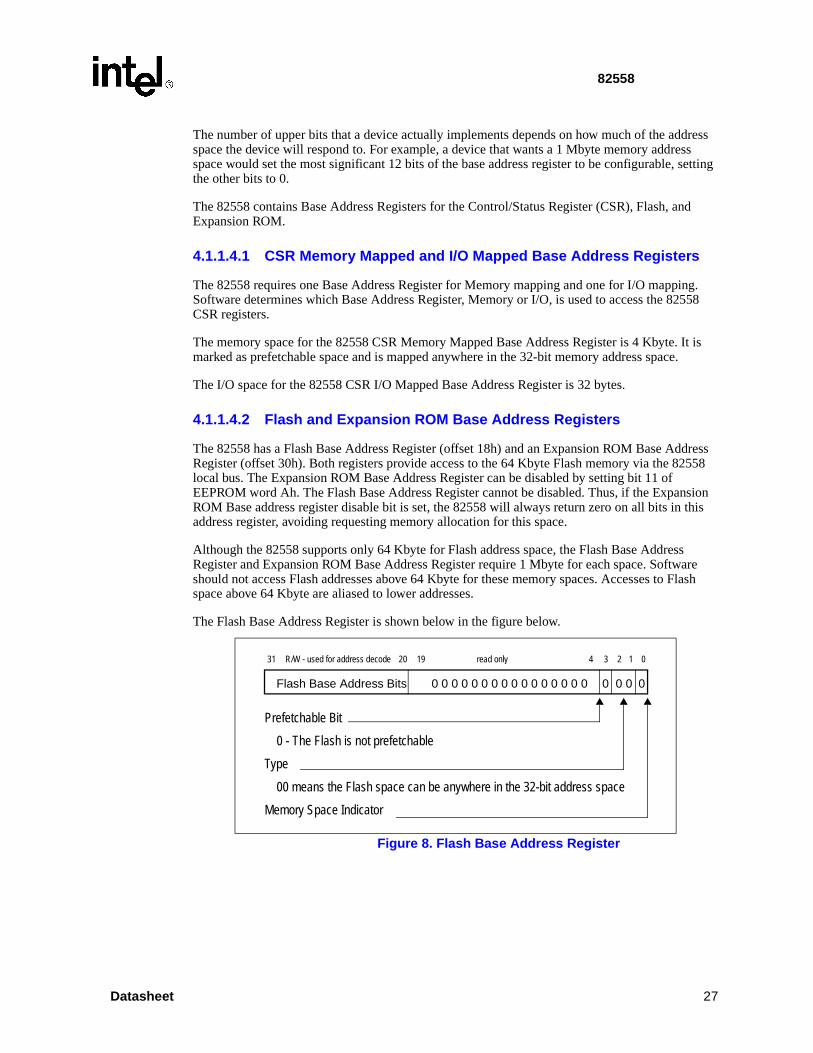
The 82558 has a Flash Base Address Register (offset 18h) and an Expansion ROM Base AdRegister (offset 30h). Both registers provide access to the 64 Kbyte Flash memory via the 82local bus. The Expansion ROM Base Address Register can be disabled by setting bit 11 of EEPROM word Ah. The Flash Base Address Register cannot be disabled. Thus, if the ExpaROM Base address register disable bit is set, the 82558 will always return zero on all bits in address register, avoiding requesting memory allocation for this space.
Although the 82558 supports only 64 Kbyte for Flash address space, the Flash Base AddresRegister and Expansion ROM Base Address Register require 1 Mbyte for each space. Softwshould not access Flash addresses above 64 Kbyte for these memory spaces. Accesses to space above 64 Kbyte are aliased to lower addresses.
The Flash Base Address Register is shown below in the figure below.
Figure 8. Flash Base Address Register
Flash Base Address Bits 0 0 0 0 0 0 0 0 0 0 0 0 0 0 0 0 0 0 0 0
R/W - used for address decode31 20 19 4 3 2 1 0read only
Prefetchable Bit
0 - The Flash is not prefetchable
Type
00 means the Flash space can be anywhere in the 32-bit address space
Memory Space Indicator
Datasheet 27
82558
t also s only gister other ter is
1b ill
t.
r, the 558, as data.
ontrol hip and serves lash
Note: The Flash is not prefetchable.
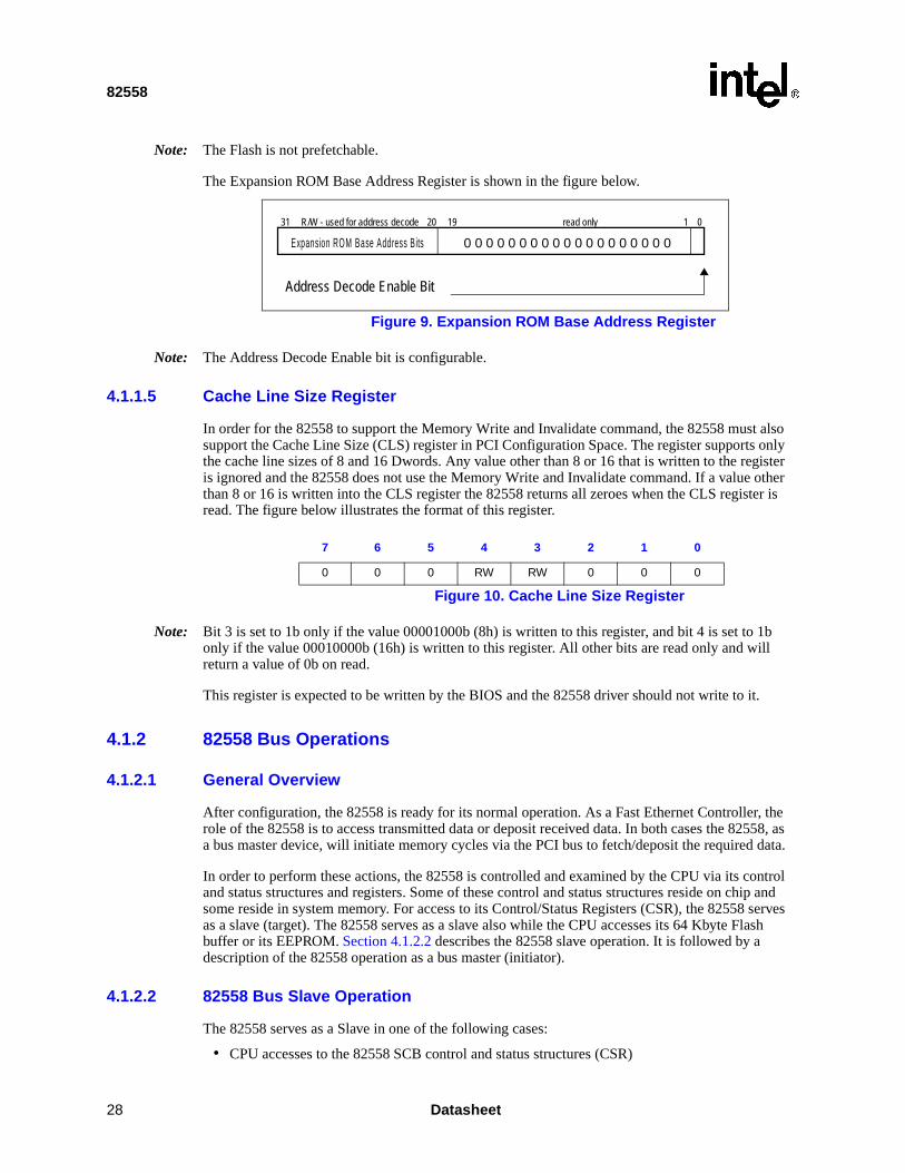
The Expansion ROM Base Address Register is shown in the figure below.
Note: The Address Decode Enable bit is configurable.
4.1.1.5 Cache Line Size Register
In order for the 82558 to support the Memory Write and Invalidate command, the 82558 mussupport the Cache Line Size (CLS) register in PCI Configuration Space. The register supportthe cache line sizes of 8 and 16 Dwords. Any value other than 8 or 16 that is written to the reis ignored and the 82558 does not use the Memory Write and Invalidate command. If a valuethan 8 or 16 is written into the CLS register the 82558 returns all zeroes when the CLS regisread. The figure below illustrates the format of this register.
Note: Bit 3 is set to 1b only if the value 00001000b (8h) is written to this register, and bit 4 is set toonly if the value 00010000b (16h) is written to this register. All other bits are read only and wreturn a value of 0b on read.
This register is expected to be written by the BIOS and the 82558 driver should not write to i
4.1.2 82558 Bus Operations
4.1.2.1 General Overview
After configuration, the 82558 is ready for its normal operation. As a Fast Ethernet Controllerole of the 82558 is to access transmitted data or deposit received data. In both cases the 82a bus master device, will initiate memory cycles via the PCI bus to fetch/deposit the required
In order to perform these actions, the 82558 is controlled and examined by the CPU via its cand status structures and registers. Some of these control and status structures reside on csome reside in system memory. For access to its Control/Status Registers (CSR), the 82558as a slave (target). The 82558 serves as a slave also while the CPU accesses its 64 Kbyte Fbuffer or its EEPROM. Section 4.1.2.2 describes the 82558 slave operation. It is followed by a description of the 82558 operation as a bus master (initiator).
4.1.2.2 82558 Bus Slave Operation
The 82558 serves as a Slave in one of the following cases:
• CPU accesses to the 82558 SCB control and status structures (CSR)
Figure 9. Expansion ROM Base Address Register
0 0 0 0 0 0 0 0 0 0 0 0 0 0 0 0 0 0 0
R/W - used for address decode31 20 19 1 0read only
Address Decode Enable Bit
Expansion ROM Base Address B its
7 6 5 4 3 2 1 0
0 0 0 RW RW 0 0 0
Figure 10. Cache Line Size Register
28 Datasheet
82558
space to ytes in y spaces
ace. lish this. se
ing the action.
• CPU accesses to the EEPROM through its control register (CSR)
• CPU accesses to the 82558 PORT address (CSR)
• CPU accesses to the MDI control register (CSR)
• CPU accesses to the Flash control register (CSR)
• CPU accesses to the 64 Kbyte Flash
The CSR and the 1 Mbyte Flash buffer are considered by the 82558 as two totally separatedmemory spaces. The 82558 provides separate Base Address Registers in the configuration distinguish between them. The size of the control and status registers memory space is 32 bthe I/O space and 4 Kbyte in the memory space. The 82558 treats accesses to these memordifferently.
4.1.2.3 Control/Status Register (CSR) Accesses
The 82558 supports zero wait state single cycle I/O or memory mapped accesses to its CSR spSeparate base address registers request 32 bytes of both memory and I/O space to accompBased on its needs, the software driver will use either I/O or memory mapping to access theregisters. The 82558 provides 32 valid bytes of CSR, which include the following elements:
• SCB
• PORT
• Flash control register
• EEPROM control register
• MDI control register
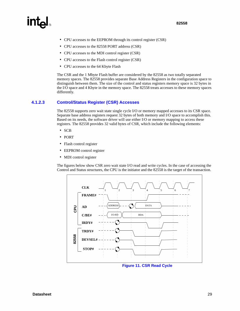
The figures below show CSR zero wait state I/O read and write cycles. In the case of accessControl and Status structures, the CPU is the initiator and the 82558 is the target of the trans
Figure 11. CSR Read Cycle
1 2 3 4 5 6 7
ADDRESS DATA
I/O-RD BE#s
CLK
FRAME#
AD
C/BE#
IRDY#
TRDY#
DEVSEL#
8255
8C
PU
STOP#
Datasheet 29

82558
byte trols o issue ect by is not
byte with RDY# issue ng the
e
Read Accesses: The CPU, as the initiator, drives the address lines AD0-31, the command andenable lines C/BE0-3# and the control lines IRDY# and FRAME#. As a slave, the 82558 conthe TRDY# signal and provides valid data on each data access. The 82558 allows the CPU tonly one read cycle when it accesses the Control and Status registers, generating a disconnasserting the STOP# signal. The CPU can insert wait states by de-asserting IRDY# when it ready.
Write Accesses: The CPU, as the initiator, drives the address lines AD0-31, the command andenable lines C/BE0-3# and the control lines IRDY# and FRAME#. It also provides the 82558valid data on each data access immediately after asserting IRDY#. The 82558 controls the Tsignal and asserts it from the data access. As for read cycles, the 82558 allows the CPU to only one I/O write cycle to the Control & Status registers, generating a disconnect by assertiSTOP# signal. This is true for both memory mapped and I/O mapped accesses.
4.1.2.4 Flash Buffer Accesses
The CPU accesses to the Flash Buffer are very slow. For this reason the 82558 issues a target-disconnect at the first data access. The 82558 asserts the STOP# signal to indicate a target-disconnect. The figures below illustrate memory CPU read and write accesses to the 64 KbytFlash buffer. The longest burst cycle to the Flash buffer contains one data access only.
Figure 12. CSR Write Cycle
FRAME#
CLK1 2 3 4 5 6 7
AD ADDRESS DATA
C/BE# I/O-WR BE#s
IRDY#
TRDY#
DEVSEL#
STOP#
8255
8C
PU
30 Datasheet

82558
d e
m the e esses
ses can
Read Accesses: The CPU, as the initiator, drives the address lines AD[31:0], the command anbyte enable lines C/BE0-3# and the control lines IRDY# and FRAME#. The 82558 controls thTRDY# signal and de-asserts it for a certain number of clocks until valid data can be read froFlash Buffer. When TRDY# is asserted, the 82558 drives valid data on the AD[31:0] lines. ThCPU can also insert wait states by de-asserting IRDY# until it is ready. Flash buffer read acccan be byte or word length.
Write Accesses: The CPU, as the initiator, drives the address lines AD0-31, the command and byte enable lines C/BE0-3# and the control lines IRDY# and FRAME#. It also provides the 82558 with valid data immediately after asserting IRDY#. The 82558 controls the TRDY# signal and de-assertsit for a certain number of clocks until valid data is written to the Flash Buffer. By asserting TRDY#, the 82558 signals the CPU that the current data access is completed. Flash buffer write accesbe byte length only.
Figure 13. Flash Buffer Read Cycle
Figure 14. Flash Buffer Write Cycle
FRAME#
CLK
AD ADDRESS
C/BE# MEM-RD BE#s
IRDY#
TRDY#
DEVSEL#
STOP#
DATA
CP
U82
558
ADDRESS DATA
MEM-WR BE#’s
FRAME#
CLK
AD
C/BE#
IRDY#
TRDY#
DEVSEL#
STOP#
CP
U82
558
Datasheet 31

82558
the e to t rder to he cur.
ted.
I et (PCI error
ption of
bit are R# or bit one
4.1.2.5 Retry Premature Accesses
As mentioned above, the 82558 responds with a Retry to any configuration cycle accessing 82558 before the completion of the automatic read of the EEPROM. The 82558 may continuRetry any configuration accesses until the EEPROM read is completed. The 82558 does noenforce the rule that the retried master must attempt to access the same address again in ocomplete any delayed transaction. Any master access to the 82558 after the completion of tEEPROM read will be honored. The figure below depicts how a Retry looks when it would oc
Note that the 82558 is considered the target in the above diagram; thus, TRDY# is not asser
4.1.2.6 Error Handling
Data Parity Errors: The 82558 checks for data parity errors while it is the target of the transaction. If an error was detected, the 82558 always sets the Detected Parity Error bit (PCStatus Register, bit 15). The 82558 also asserts PERR#, if the Parity Error Response bit is sCommand Register, bit 6). The 82558 does not attempt to terminate a cycle in which a paritywas detected. This gives the initiator of the access, at each hardware or software level, the orecovery.
Target-Disconnect: The 82558 will use premature termination in the following cases:
• After accesses to the 64 Kbyte Flash buffer.
• After accesses to its CSR.
• After accesses to the configuration space
System Error: The 82558 reports parity error on address phase using the SERR# pin. If the SERR# Enable bit (in the PCI-configuration command register) or the Parity Error Response not set, the 82558 only sets the Detected Parity Error bit (PCI Status Register, bit 15). If SEREnable and Parity Error Response bits are both set, the 82558 sets the Signaled System Err(PCI Status Register, bit 14) as well as the Detected Parity Error bit and asserts SERR# for clock.
Figure 15. PCI Retry Cycle
FRAME#
CLK
STOP#
TRDY#
IRDY#
DEVSEL#
32 Datasheet

82558
ction
is
posit s zero
host arget.
ide in emory es to
The 82558, when detecting system error, will claim the cycle if it was the target of the transaand continue the transaction as though the address was correct.
Note: The 82558 will report a system error for any parity error on address phase, whether or not it involved in the current transaction.
4.1.2.7 82558 Bus Master Operation
As a PCI Bus Master, the 82558 initiates memory cycles to fetch data for transmission or dereceived data and for accessing the memory resident control structures. The 82558 performwait state burst read and write cycles to the host main memory. Figure 16 and Figure 17 depict memory read and write burst cycles. For bus master cycles, the 82558 is the initiator and themain memory (or the PCI Host Bridge depending on the configuration of the systems) is the t
The CPU provides the 82558 with action commands and pointers to the data buffers that reshost main memory. The 82558 independently manages these structures and initiates burst mcycles to transfer data to and from them. The 82558 uses MEM-RD Multiple for burst access
Figure 16. Memory Read Burst Cycle
Figure 17. Memory Write Burst Cycle
8255
8C
PU
CLK
FRAME#
C/BE#
IRDY#
TRDY#
DEVSEL#
AD
3 421 5 6 7 8 9 10
ADDR DATA
MEM-RD BE# BE#
DATA DATA DATA DATA
8255
8C
PU
CLK
FRAME#
C/BE#
IRDY#
TRDY#
DEVSEL#
AD
3 421 5 6 7 8 9 10
ADDR DATA
MEM-WR BE# BE#
DATA DATA DATA DATA
Datasheet 33

82558
s, . For .
form
the
lines C/ wait ng the
ally ternal
lines C/ wait (from by de-
he
signal
nnect, he ld
the DY#
s on
r e . In y Error
data buffers and MEM-RD LINE for burst accesses to control structures (commands, pointeretc.). For all write accesses to the control structure, the 82558 uses the MEM-WR commandwrite accesses to data structure, the 82558 may use either the MEM-WR or MWI commands
Read Accesses: The 82558 performs block transfers from host system memory in order to perframe transmission on the serial link. In this case, the 82558 initiates zero wait state memory read burst cycles for these accesses. The length of a burst is bounded by the system and also by82558 internal FIFO. The length of a read burst may also be bounded by the TX DMA MAXIMUM BYTE COUNT in the Configuration command.
The 82558, as the initiator, drives the address lines AD0-31, the command and byte enable BE0-3# and the control lines IRDY# and FRAME#. The 82558 asserts IRDY# to support zerostate burst cycles. The target signals the 82558 that valid data is ready to be read by assertiTRDY# signal.
Write Accesses: The 82558 performs block transfers to host system memory during frame reception. In this case, the 82558 initiates memory write burst cycles to deposit the data, usuwithout wait states. The length of a burst is bounded by the system and also by the 82558 inFIFO threshold. The length of a write burst may also be bounded by the RX DMA MAXIMUMBYTE COUNT in the Configuration command.
The 82558, as the initiator, drives the address lines AD0-31, the command and byte enable BE0-3# and the control lines IRDY# and FRAME#. The 82558 asserts IRDY# to support zerostate burst cycles. The 82558 also drives valid data on AD0-31 lines during each data phasethe first clock and on). The target controls the length and signals completion of a data phaseassertion and assertion of TRDY#.
Cycle Completion: The 82558 completes (terminates) its initiated memory burst cycles in thefollowing cases:
Normal Completion: all data involved in the transaction has been transferred to or from ttarget (for example, host main memory).
Backoff: the Latency Timer has expired and the arbiter has removed the 82558 bus grant(GNT#), indicating that the 82558 has been preempted by another bus master.
TX or RX DMA MAXIMUM BYTE COUNT: the 82558 burst has reached the length specified in the TX or RX DMA MAXIMUM BYTE COUNT field in the configuration block.Refer to the 82558 Software Developer’s Manual for more detailed information.
Target Termination: the target may request to terminate the transaction with target-discotarget-retry, or target-abort. In the first two cases, the 82558 initiates the cycle again. In tcase of a Target Abort, the 82558 sets the Received Target Abort bit in the PCI Status fie(PCI Status Register, bit 12) and does not re-initiate the cycle.
Master Abort: the target of the transaction has not responded to the address initiated by82558 (DEVSEL# has not been asserted). The 82558 simply de-asserts FRAME# and IRas in the case of normal completion.
Error Condition: in the event of parity or any other system error detection, the 82558 completes its current initiated transaction. Any further action taken by the 82558 dependthe type of error and other conditions.
Data Parity Errors: As an initiator, the 82558 checks and detects data parity errors that occuduring a transaction. If the Parity Error Response bit is set (PCI Command Register, bit 6), th82558 also asserts PERR# and sets the Data Parity Detected bit (PCI Status Register, bit 8)addition, if the error was detected by the 82558 during read cycles, it sets the Detected Paritbit (PCI Status Register, bit 15).
34 Datasheet
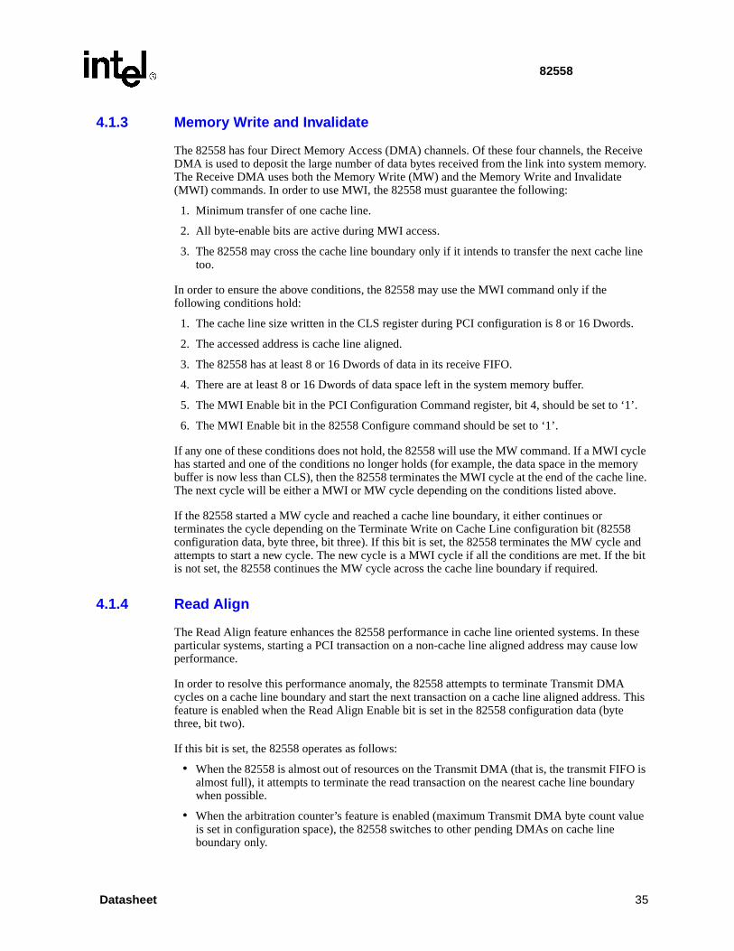
82558
ceive mory.
e line
s.
1’.
ycle mory e line.
58 and e bit
these e low
ss. This e
FO is dary
alue
4.1.3 Memory Write and Invalidate
The 82558 has four Direct Memory Access (DMA) channels. Of these four channels, the ReDMA is used to deposit the large number of data bytes received from the link into system meThe Receive DMA uses both the Memory Write (MW) and the Memory Write and Invalidate (MWI) commands. In order to use MWI, the 82558 must guarantee the following:
1. Minimum transfer of one cache line.
2. All byte-enable bits are active during MWI access.
3. The 82558 may cross the cache line boundary only if it intends to transfer the next cachtoo.
In order to ensure the above conditions, the 82558 may use the MWI command only if the following conditions hold:
1. The cache line size written in the CLS register during PCI configuration is 8 or 16 Dword
2. The accessed address is cache line aligned.
3. The 82558 has at least 8 or 16 Dwords of data in its receive FIFO.
4. There are at least 8 or 16 Dwords of data space left in the system memory buffer.
5. The MWI Enable bit in the PCI Configuration Command register, bit 4, should be set to ‘
6. The MWI Enable bit in the 82558 Configure command should be set to ‘1’.
If any one of these conditions does not hold, the 82558 will use the MW command. If a MWI chas started and one of the conditions no longer holds (for example, the data space in the mebuffer is now less than CLS), then the 82558 terminates the MWI cycle at the end of the cachThe next cycle will be either a MWI or MW cycle depending on the conditions listed above.
If the 82558 started a MW cycle and reached a cache line boundary, it either continues or terminates the cycle depending on the Terminate Write on Cache Line configuration bit (825configuration data, byte three, bit three). If this bit is set, the 82558 terminates the MW cycleattempts to start a new cycle. The new cycle is a MWI cycle if all the conditions are met. If this not set, the 82558 continues the MW cycle across the cache line boundary if required.
4.1.4 Read Align
The Read Align feature enhances the 82558 performance in cache line oriented systems. Inparticular systems, starting a PCI transaction on a non-cache line aligned address may causperformance.
In order to resolve this performance anomaly, the 82558 attempts to terminate Transmit DMAcycles on a cache line boundary and start the next transaction on a cache line aligned addrefeature is enabled when the Read Align Enable bit is set in the 82558 configuration data (bytthree, bit two).
If this bit is set, the 82558 operates as follows:
• When the 82558 is almost out of resources on the Transmit DMA (that is, the transmit FIalmost full), it attempts to terminate the read transaction on the nearest cache line bounwhen possible.
• When the arbitration counter’s feature is enabled (maximum Transmit DMA byte count vis set in configuration space), the 82558 switches to other pending DMAs on cache line boundary only.
Datasheet 35

82558
cause
set to
the
to a 64 stem
d or a o the d. Refer sses to her the OM Flash
is f two ss to the
ss on
f the the
ddress ast ur
ed by the by the tely
er the o avoid hich
d one
Note the following:
• This feature is not recommended for use in non-cache line oriented systems since it mayshorter bursts and lower performance.
• This feature should be used only when cache line size filled in PCI configuration space is8 or 16.
• The 82558 reads all its control data structures (including Receive Buffer Descriptors) fromfirst Dword (even if it is not required) in order to maintain cache line alignment.
4.2 Flash/EEPROM Interface
The local memory interface consists of an interface to a Flash (or EPROM) and an interface serial EEPROM. The 82558 provides address decoding and control to allow access to up to Kbyte of Flash. The EEPROM is used to store information such as configurations bits, SubsyID, Subsystem Vendor ID, Node Individual Address and board configuration.
4.2.1 Flash Interface
The Flash (or Boot EPROM) is read from or written to whenever the host CPU performs a reawrite operation to a memory location that is within the Flash mapping window. All accesses tFlash, except read accesses, require the appropriate command sequence for the device useto the specific Flash data sheet for more details on reading from or writing to Flash. The accethe Flash are based on a direct decode of CPU accesses to a memory window defined in eit82558 Flash Base Address Register (PCI Control Register at offset 18h) or the Expansion RBase Address Register (PCI Control Register at offset 30h). The 82558 asserts control to thewhen it decodes a valid access.
The 82558 supports an external Flash memory (or Boot ROM) of up to 64 Kbyte. The Flash accessed by eight multiplexed address pins and eight data pins. Each access is comprised oaddress cycles, one data cycle, and then zero to three pairs of address and data cycles. AcceFlash is as follows:
1. At the first address cycle, the 82558 provides the eight most significant bits of the addrethe eight Flash address pins FLADDR[7:0].
2. The 82558 then asserts the FLCS# signal (low) which latches the most significant bits oaddress into an external 8-bit latch. The output pins of the latch should be connected to eight most significant bits of the address of the 64 Kbyte Flash.
3. During the second address phase, the 82558 provides the 8 least significant bits of the aon FLADDR[7:0]. If the access consists of more than one byte, the 82558 modifies the lesignificant bits of the address and reads/writes the next byte, up to a maximum total of fobytes.
The access to the Flash can be done by either accessing the Flash address space, as definFlash Base Address Register (offset 18h), or the Expansion ROM address space, as definedExpansion ROM Address Register (offset 30h). The Expansion ROM address can be separadisabled by setting the corresponding bit in EEPROM word Ah.
Note that Flash accesses must always be assembled or disassembled by the 82558 whenevaccess is greater than a byte-wide access. Due to slow access times to a typical Flash and tviolating PCI bus holding specifications (no more than 16 wait states inserted for any cycles ware not system initiation cycles), the maximum data size is two bytes for a read operation anbyte for a write operation.
36 Datasheet
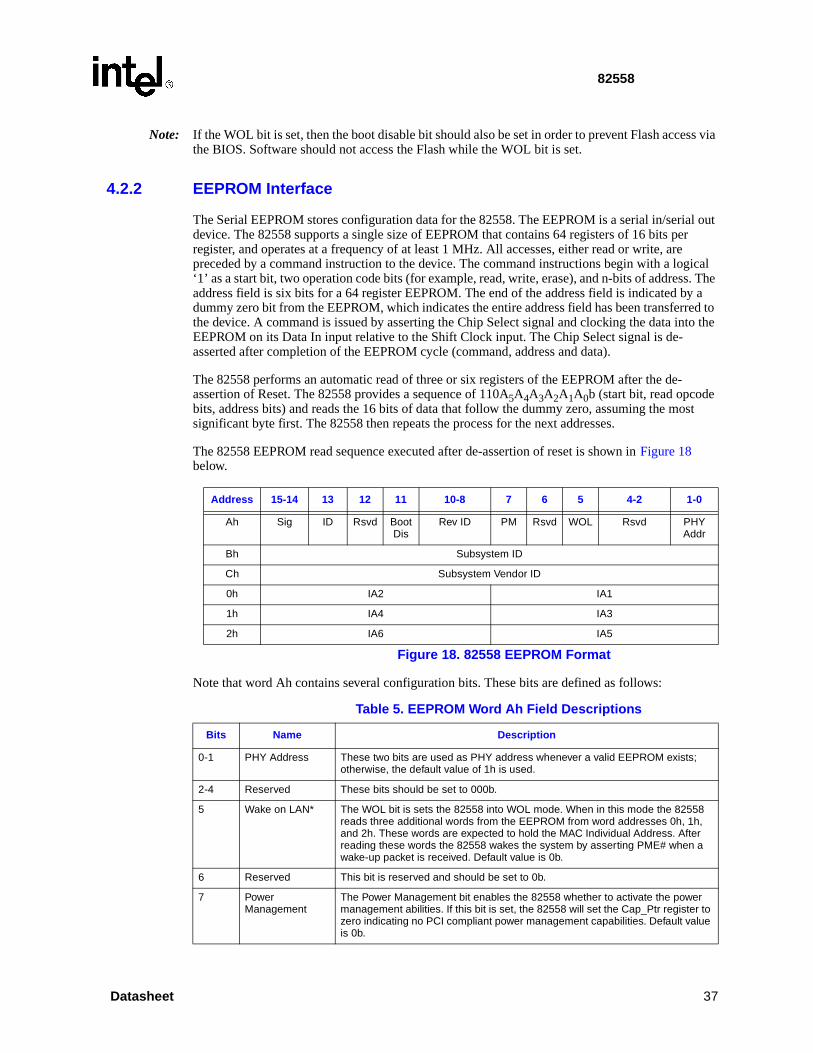
82558
ess via
al out r
e gical s. The y a red to
nto the
ost
Note: If the WOL bit is set, then the boot disable bit should also be set in order to prevent Flash accthe BIOS. Software should not access the Flash while the WOL bit is set.
4.2.2 EEPROM Interface
The Serial EEPROM stores configuration data for the 82558. The EEPROM is a serial in/seridevice. The 82558 supports a single size of EEPROM that contains 64 registers of 16 bits peregister, and operates at a frequency of at least 1 MHz. All accesses, either read or write, arpreceded by a command instruction to the device. The command instructions begin with a lo‘1’ as a start bit, two operation code bits (for example, read, write, erase), and n-bits of addresaddress field is six bits for a 64 register EEPROM. The end of the address field is indicated bdummy zero bit from the EEPROM, which indicates the entire address field has been transferthe device. A command is issued by asserting the Chip Select signal and clocking the data iEEPROM on its Data In input relative to the Shift Clock input. The Chip Select signal is de-asserted after completion of the EEPROM cycle (command, address and data).
The 82558 performs an automatic read of three or six registers of the EEPROM after the de-assertion of Reset. The 82558 provides a sequence of 110A5A4A3A2A1A0b (start bit, read opcode bits, address bits) and reads the 16 bits of data that follow the dummy zero, assuming the msignificant byte first. The 82558 then repeats the process for the next addresses.
The 82558 EEPROM read sequence executed after de-assertion of reset is shown in Figure 18 below.
Note that word Ah contains several configuration bits. These bits are defined as follows:
Address 15-14 13 12 11 10-8 7 6 5 4-2 1-0
Ah Sig ID Rsvd Boot Dis
Rev ID PM Rsvd WOL Rsvd PHY Addr
Bh Subsystem ID
Ch Subsystem Vendor ID
0h IA2 IA1
1h IA4 IA3
2h IA6 IA5
Figure 18. 82558 EEPROM Format
Table 5. EEPROM Word Ah Field Descriptions
Bits Name Description
0-1 PHY Address These two bits are used as PHY address whenever a valid EEPROM exists; otherwise, the default value of 1h is used.
2-4 Reserved These bits should be set to 000b.
5 Wake on LAN* The WOL bit is sets the 82558 into WOL mode. When in this mode the 82558 reads three additional words from the EEPROM from word addresses 0h, 1h, and 2h. These words are expected to hold the MAC Individual Address. After reading these words the 82558 wakes the system by asserting PME# when a wake-up packet is received. Default value is 0b.
6 Reserved This bit is reserved and should be set to 0b.
7 Power Management
The Power Management bit enables the 82558 whether to activate the power management abilities. If this bit is set, the 82558 will set the Cap_Ptr register to zero indicating no PCI compliant power management capabilities. Default value is 0b.
Datasheet 37

82558
y if iltering
y .
Hz) to 2558 e
Note: The shaded area defines the difference in the 82558 B-step from the 82558 A-step.
Note that words 0h, 1h, and 2h, the Individual Address (IA) bytes, are read by the 82558 onlWOL bit is set. When read, the words are stored in the 82558 and used for receive address fand transmit source address insertion.
The IA read from the EEPROM is used by the 82558 until an IA-Setup command is issued bsoftware. The IA defined by the IA-Setup command overrides the IA read from the EEPROM
The 82558 EEPROM read is approximately 6000 CLK clocks long (180 microseconds at 33 Mor 12000 CLK clocks in WOL mode (360 microseconds at 33 MHz). The system is required provide a valid clock on the CLK pin for this time period after RST# de-assertion even if the 8has its ISOLATE# pin asserted (the CLK input is not isolated until the EEPROM accesses arcomplete).
8-10 Revision ID These three bits are used as the three least significant bits of the device revision, if bits 15 and 14 are set to 01b and the ID was set as described in Section 4.1.1.3, “Device ID and System ID Registers” on page 24. The default value depends on the silicon revision.
8-10 Revision ID
(B-step only)
These three bits are used as the three least significant bits of the device revision, if bits 15, 14, and 13 equal 011b and the ID was set as described in Section 4.1.1.3, “Device ID and System ID Registers” on page 24. The default value depends on the silicon revision.
11 Boot Disable The Boot Disable bit disables the Expansion ROM Base Address Register (Address 30h) when it is set. Default value is 0b.
12 Reserved This bit is reserved and should be set to 0b.
13 ID The ID bit indicates how the Subsystem ID and Subsystem Vendor ID fields are used as described in Section 4.1.1.3, “Device ID and System ID Registers” on page 24. Default value is 0b.
14-15 Signature The Signature field is a signature of 01b, indicating to the 82558 that there is a valid EEPROM present. If the Sig field is not 01b, the other bits are ignored and the default values are used.
Table 5. EEPROM Word Ah Field Descriptions
Bits Name Description
38 Datasheet

82558
.3u
rnal
ial
sly.
n the
th the
y rnal ex
d
EEPROM read instruction waveform is shown in the figure below.
4.3 10/100 Mbps CSMA/CD Unit
The 82558 CSMA/CD unit implements both the IEEE 802.3 Ethernet 10 Mbps and IEEE 802Fast Ethernet 100 Mbps standards. It performs all the CSMA/CD protocol functions such as transmission, reception, collision handling, etc. The 82558 CSMA/CD unit interfaces the intePHY unit through a standard Media Independent Interface (MII), as specified by IEEE 802.3 chapter 22, This is a 10/100 Mbps mode in which the data stream is nibble-wide and the serclocks run at either 25 or 2.5 MHz.
4.3.1 Full Duplex
When operating in full duplex mode the 82558 can transmit and receive frames simultaneou
Transmission starts regardless of the state of the internal receive path. Reception starts wheinternal PHY detects a valid frame on the RCV pair of the PHY.
The 82558 operates in either half duplex mode or full duplex mode. For proper operation, bo82558 CSMA module and the PHY unit must be set to the same duplex mode.
The CSMA duplex mode is set by the 82558 Configure command or forced by automaticallytracking the mode in the PHY unit.
The PHY duplex mode is set either by Auto-Negotiation or, if Auto-Negotiation is disabled, bsetting the Full duplex bit in the MMI register (register #0 bit #8). Note that by default, the intePHY unit advertises full duplex ability in the Auto-Negotiation process regardless of the duplsetting of the CSMA unit. The CSMA configuration should match the result of the Auto-Negotiation.
The selection of duplex operation (full or half) and flow control is done in two levels: MAC anPHY.
Figure 19. EEPROM Read Instruction Waveform
A 1A 0
E E C S
E E S K
EEDI
E E D O
A 5 A 4 A 2
D 1 5 D 0
READ OP code
A 3 A 1 A 0
Datasheet 39

82558
ched
PHY
here ive FC
or -
the f its IA
n of es. s as
The MAC duplex selection is done only through CSMA configuration mechanism (configure command from the software).
4.3.2 Flow Control
The 82558 supports frame based flow control frames in both full duplex and half duplex switenvironments. The 82558 flow control feature is not intended to be used in shared media environments.
The 82558 supports two methods of Flow Control (FC) while operating in full duplex:
• PHY based Flow Control
• Frame based Flow Control
The 82558 supports the PHY based FC only when operating in PHY mode using its internal unit.
FC is optional in FDX mode and also can be selected only through software configuration. Tare four modes for flow control: PHY based FC, frame-based-transmit FC, frame-based-receand none. Frame based transmit and receive can be selected
PHY duplex and frame based FC enable is selected using NWay* Auto-Negotiation algorithmthrough the Management Data Interface. The 82558 default ability advertisement in the AutoNegotiation process is capable of PHY based FC.
The two flow control methods should not be used at the same time.
4.3.3 Address Filtering Modifications
The 82558 can be configured to ignore one bit when checking for its IA on incoming receive frames. The address bit is the second least significant bit of the first byte of the IA, known asUpper/Lower (U/L) bit. This bit may be used in some cases as a priority indication bit. Whenconfigured to do so, the 82558 passes any frame that matches all the other 47 address bits oregardless of the value of the U/L bit.
Note that this configuration only affects the 82558 specific IA and not multicast, multi-IA or broadcast address filtering.
The 82558 does not attribute any priority to frames with this bit set, it simply passes them tomemory regardless of this bit.
4.3.4 VLAN Support
The 82558 supports the emerging VLAN standard currently being defined by the IEEE 802.1committee. All VLAN flows will be implemented by software. The 82558 supports the receptiolong frames, specifically frames longer than 1.5 kilobits. However, it marks them as bad framThe change was the addition of a configuration in which the 82558 does not mark long framebad frames.
40 Datasheet
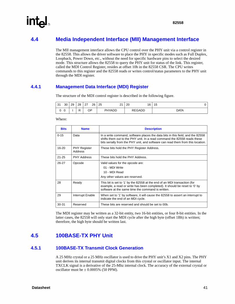
82558
er in uplex, d
ter,
Y unit
the
HY l al or
4.4 Media Independent Interface (MII) Management Interface
The MII management interface allows the CPU control over the PHY unit via a control registthe 82558. This allows the driver software to place the PHY in specific modes such as Full DLoopback, Power Down, etc., without the need for specific hardware pins to select the desiremode. This structure allows the 82558 to query the PHY unit for status of the link. This regiscalled the MDI Control Register, resides at offset 10h in the 82558 CSR. The CPU writes commands to this register and the 82558 reads or writes control/status parameters to the PHthrough the MDI register.
4.4.1 Management Data Interface (MDI) Register
The structure of the MDI control register is described in the following figure.
Where:
The MDI register may be written as a 32-bit entity, two 16-bit entities, or four 8-bit entities. Inlatter cases, the 82558 will only start the MDI cycle after the high byte (offset 1Bh) is written;therefore, the high byte should be written last.
4.5 100BASE-TX PHY Unit
4.5.1 100BASE-TX Transmit Clock Generation
A 25 MHz crystal or a 25 MHz oscillator is used to drive the PHY unit’s X1 and X2 pins. The Punit derives its internal transmit digital clocks from this crystal or oscillator input. The internaTXCLK signal is a derivative of the 25-Mhz internal clock. The accuracy of the external crystoscillator must be ± 0.0005% (50 PPM).
31 30 29 28 27 26 25 21 20 16 15 0
0 0 I R OP PHYADD REGADD DATA
Bits Name Description
0-15 Data In a write command, software places the data bits in this field, and the 82558 shifts them out to the PHY unit. In a read command the 82558 reads these bits serially from the PHY unit, and software can read them from this location.
16-20 PHY Register Address
These bits hold the PHY Register Address.
21-25 PHY Address These bits hold the PHY Address.
26-27 Opcode Valid values for the opcode are:
01 - MDI Write
10 - MDI Read
Any other values are reserved.
28 Ready This bit is set to ‘1’ by the 82558 at the end of an MDI transaction (for example, a read or write has been completed). It should be reset to ‘0’ by software at the same time the command is written.
29 Interrupt Enable When set to ‘1’ by software, it will cause the 82558 to assert an interrupt to indicate the end of an MDI cycle.
30-31 Reserved These bits are reserved and should be set to 00b.
Datasheet 41
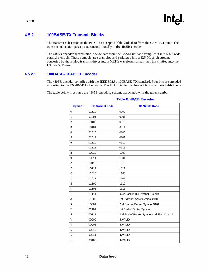
82558
he
ide
the
oded code.
4.5.2 100BASE-TX Transmit Blocks
The transmit subsection of the PHY unit accepts nibble-wide data from the CSMA/CD unit. Ttransmit subsection passes data unconditionally to the 4B/5B encoder.
The 4B/5B encoder accepts nibble-wide data from the CSMA unit and compiles it into 5-bit-wparallel symbols. These symbols are scrambled and serialized into a 125-Mbps bit stream, converted by the analog transmit driver into a MLT-3 waveform format, then transmitted into UTP or STP wire.
4.5.2.1 100BASE-TX 4B/5B Encoder
The 4B/5B encoder complies with the IEEE 802.3u 100BASE-TX standard. Four bits are encaccording to the TX 4B/5B lookup table. The lookup table matches a-5 bit code to each 4-bit
The table below illustrates the 4B/5B encoding scheme associated with the given symbol.
Table 6. 4B/5B Encoder
Symbol 5B Symbol Code 4B Nibble Code
0 11110 0000
1 01001 0001
2 10100 0010
3 10101 0011
4 01010 0100
5 01011 0101
6 01110 0110
7 01111 0111
8 10010 1000
9 10011 1001
A 10110 1010
B 10111 1011
C 11010 1100
D 11011 1101
E 11100 1110
F 11101 1111
I 11111 Inter Packet Idle Symbol (No 4B)
J 11000 1st Start of Packet Symbol 0101
K 10001 2nd Start of Packet Symbol 0101
T 01101 1st End of Packet Symbol
R 00111 2nd End of Packet Symbol and Flow Control
V 00000 INVALID
V 00001 INVALID
V 00010 INVALID
V 00011 INVALID
H 00100 INVALID
42 Datasheet
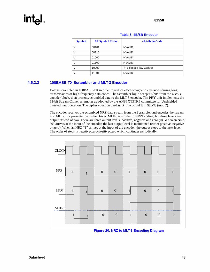
82558
/5B ts the
stream NRZ
ative vel.
4.5.2.2 100BASE-TX Scrambler and MLT-3 Encoder
Data is scrambled in 100BASE-TX in order to reduce electromagnetic emissions during longtransmissions of high-frequency data codes. The Scrambler logic accepts 5 bits from the 4Bencoder block, then presents scrambled data to the MLT-3 encoder. The PHY unit implemen11-bit Stream Cipher scrambler as adopted by the ANSI XT3T9.5 committee for UnshieldedTwisted Pair operation. The cipher equation used is: X[n] = X[n-11] + X[n-9] (mod 2).
The encoder receives the scrambled NRZ data stream from the Scrambler and encodes theinto MLT-3 for presentation to the Driver. MLT-3 is similar to NRZI coding, but three levels areoutput instead of two. There are three output levels: positive, negative and zero (0). When an“0” arrives at the input of the encoder, the last output level is maintained (either positive, negor zero). When an NRZ “1” arrives at the input of the encoder, the output steps to the next leThe order of steps is negative-zero-positive-zero which continues periodically.
V 00101 INVALID
V 00110 INVALID
V 01000 INVALID
V 01100 INVALID
V 10000 PHY based Flow Control
V 11001 INVALID
Table 6. 4B/5B Encoder
Symbol 5B Symbol Code 4B Nibble Code
Figure 20. NRZ to MLT-3 Encoding Diagram
1011 0 00 1
CLOCK
MLT-3
NRZI
NRZ
1011 0 00 1
1011 0 00 1
Datasheet 43

82558
e, l, e after ta into
the s for
ould from
4.5.2.3 100BASE-TX Transmit Framing
The PHY unit does not differentiate between the fields of the MAC frame containing preamblSFD, data and CRC. The PHY unit encodes the first byte of the preamble as the “JK” symboencodes all other pieces of data according to the 4B/5B lookup table, and adds the “TR” codthe end of the packet (de-assertion of TXEN). The PHY unit scrambles and serializes the daa 125-Mbps stream, encodes it as MLT-3, and drives it onto the wire.
4.5.2.4 Transmit Driver
The TD pair lines are implemented with a digitally slope controlled current driver that meets TP-PMD specifications. Current is sinked from the isolation transformer by the TDP and TDNpins. The total current sinked into Vss pins is a constant 40mA. Conceptual transmit waveform100 Mbps are given in the following figure.
The magnetics module that is external to the PHY unit converts ITDP and ITDN to the 2.0 Vpp, as required by the TP-PMD specification. The same magnetics used for 100BASE-TX mode shalso work in 10BASE-T mode. The following is a list of current magnetics modules available several vendors:
Figure 21. Transmit Waveforms (conceptual)
(VTDP -VTDN )
+1V
0V
-1V
40mA
ITDP
20mA
0
40mA
20mA
0
ITDN
t
t
t
Table 7. Magnetics Modules
Vendor Model/Type 100BASE-TX 10BASE-T
Delta LF8200A Yes Yes
Pulse Engineering PE-68515 Yes Yes
44 Datasheet

82558
e to ata
t
jitter LT-3
ls bit coder.
e, LE s are “JK”
S”),
s.
4.5.3 100BASE-TX Receive Blocks
The receive subsection of the PHY unit accepts 100BASE-TX MLT-3 data on the RD pair. Duthe advanced DSP design techniques employed, the PHY unit will accurately receive valid dfrom CAT5 UTP and type 1 STP cable of length well in excess of 100 meters.
4.5.3.1 Adaptive Equalizer
The distorted MLT-3 signal at the end of the wire is restored by the equalizer. The equalizer performs adaptation based on the shape of the received signal, equalizing the signal to meesuperior DDJ (Data Dependent Jitter) performance.
4.5.3.2 Receive Clock and Data Recovery
The clock recovery circuit uses advanced DSP technology to compensate for various signal causes. The circuit recovers the 125 MHz clock and the data, and presents the data to the Mdecoder.
4.5.3.3 MLT-3 Decoder, Descrambler, and Receive Digital Section
The PHY unit first decodes the MLT-3 data, then the Descrambler reproduces the 5B symbooriginated in the transmitter. The descrambling is based on synchronizing to the transmit 11-LFSR (Linear Feedback Shift Register) during idle. Then the data is decoded at the 4B/5B deOnce the 4B symbols are obtained, the PHY unit outputs the receive data to the CSMA unit.
4.5.3.4 100BASE-TX Receive Framing
The PHY unit does not differentiate between the fields of the MAC frame containing preamblSFD, data and CRC. During 100 Mbps reception, the PHY unit differentiates between the IDcondition ("L" symbols on the wire) and the preamble or SFD. When two non-consecutive bit0 within 10 bits (125 Mbps 5B data coding) the PHY unit immediately asserts CRS. When thesymbols (“11000, 10001”) are fully recognized, the PHY unit asserts the RXDV signal and provides the received data to the CSMA unit. If the “JK” symbol is not recognized (“false CRCRS is immediately de-asserted and an RXER is indicated.
4.5.3.5 100BASE-TX Receive Error Detection and Reporting
In 100BASE-TX mode, the PHY unit can detect errors in the receive data in a number of wayAny of the following conditions is considered an error:
• Link integrity fails in the middle of a reception
• The SSD (“JK”) symbol is not fully detected after idle
• An invalid symbol is detected at the 4B/5B decoder
• IDLE is detected in the middle of a frame (before “TR” is detected)
Pulse Engineering H1012 Yes Yes
Table 7. Magnetics Modules
Vendor Model/Type 100BASE-TX 10BASE-T
Datasheet 45

82558
and
SE-T
the d the
TX)
may be
e the e
link d PHY he
When any of the above error conditions occurs, the PHY unit immediately asserts its RXER indication to the CSMA unit. The RXER indication is held active as long as the receive error condition persists on the receive pair.
4.5.4 100BASE-TX Collision Detection
100BASE-TX collisions (half duplex mode only) are detected much the same as they are in 10BASE-T, by simultaneous transmission and reception.
4.5.5 100BASE-TX Link Integrity and Auto-Negotiation Solution
The Auto-Negotiation function automatically configures the device to the technology, media, speed for working with its partner at the other end of the wire. Auto-Negotiation is widely discussed in IEEE specification 802.3u, clause 28. The PHY unit supports 10BASE-T, 10BAFDX, 100BASE-TX, and 100BASE-TX FDX.
The PHY unit has two Physical Media Attachment (PMA) technologies with its link integrity function, 10BASE-T and 100BASE-TX.
4.5.5.1 Link Integrity
In 100BASE-TX, the link integrity function is determined by a stable signal status coming fromTP-PMD block. Signal status is asserted when the PMD detects breaking squelch energy anright BER according to the ANSI specification.
4.5.5.2 Auto-Negotiation
The PHY unit fully supports IEEE802.3u clause 28. The technology (10BASE-T or 100BASE-will be determined by the Auto-Negotiation result.
Speed and duplex autoselect are functions of Auto-Negotiation. However, these parameters manually configured via the MMI.
4.5.6 Auto 10/100 Mbps Speed Selection
The MAC may either allow the PHY unit to automatically select its speed to operation or forcPHY into 10 Mbps or 100 Mbps mode. The Management Data Interface (MDI) can control thPHY unit speed mode.
The PHY unit autoselect function determines the operation speed of the media based on theintegrity pulses it receives (Parallel Detection). If no Fast Link Pulses (FLPs) are detected anNormal Link Pulses (NLPs) are detected, the PHY unit defaults to 10 Mbps operation. If the unit detects a speed change, it dynamically changes its TXCLK and RXCLK frequencies to tappropriate value. This change takes a maximum of five milliseconds.
46 Datasheet

82558
-Mhz 5
z ion. If om then
d t
bit a pre- the row e
he d z/
ation hat er is ata, ard.
4.6 10BASE-T Functionality
4.6.1 10BASE-T Transmit Clock Generation
The 20 MHz and 10 MHz clocks needed for 10BASE-T are synthesized from the external 25crystal or oscillator. The PHY unit provides the TXCLK and RXCLK to the internal MAC at 2.MHz.
4.6.2 10BASE-T Transmit Blocks
4.6.2.1 10BASE-T Manchester Encoder
After the 2.5 MHz clocked data TXD[3:0] is serialized in a 10 Mbps serial stream, the 20 MHclock performs the Manchester encoding. The Manchester code always has a mid-bit transitthe value is “1” then the transition is from low to high. If the value is “0” then the transition is frhigh to low. The boundary transition occurs only when the data changes from bit to bit: if “10” the change is from high to low; if “01” then the change is from low to high.
4.6.2.2 10BASE-T Driver and Filter
Since 10BASE-T and 100BASE-TX have different filtration needs, both filters are implementeinside the chip. This allows the two technologies to share the same magnetics. The PHY unisupports both technologies through one pair of TD pins and by externally sharing the same magnetics.
In 10 Mbps mode, the PHY unit begins transmitting the serial Manchester bit stream within 3times (300 nanoseconds) after the MAC asserts TXEN. In 10 Mbps mode the line drivers usedistortion algorithm to improve jitter tolerance. The line drivers reduce their drive level duringsecond half of “wide” (100ns) Manchester pulses and maintain a full drive level during all nar(50ns) pulses and the first half of the wide pulses. This reduces line overcharging during widpulses, a major source of jitter.
4.6.3 10BASE-T Receive Blocks
4.6.3.1 10BASE-T Manchester Decoder
The PHY unit performs Manchester decoding and timing recovery when in 10 Mbps mode. TManchester-encoded data stream is decoded from the RD pair to separate Receive Clock anReceive Data from the differential signal. This data is transferred to the CSMA unit at 2.5 MHnibble. The high-performance circuitry of the PHY unit exceeds the IEEE 802.3 jitter requirements.
4.6.3.2 10BASE-T Twisted Pair Ethernet (TPE) Receive Buffer and Filter
In 10 Mbps mode, data is expected to be received on the RD pair, after passing through isoltransformers. The filter is implemented inside the PHY unit for supporting single magnetics tare shared with the 100BASE-TX side. The input differential voltage range for the TPE receivgreater than 585mV and less than 3.1 V. The TPE receive buffer distinguishes valid receive dlink test pulses, and the idle condition, according to the requirements of the 10BASE-T stand
The following line activity is determined to be inactive and is rejected:
Datasheet 47
82558
han 2
l z.
0
lses,
is
e is
n. If
hose mal from f it is,
e d 39 her
the ving
d
• Differential pulses of peak magnitude less than 300 mV.
• Continuous sinusoids with a differential amplitude less than 6.2 Vpp and frequency less tMHz.
• Sine waves of a single cycle duration starting with phase 0 or 180 that have a differentiaamplitude less than 6.2 Vpp and a frequency of at least 2 MHz and not more than 16 MHThese single-cycle sine waves are discarded only if they are preceded by 4 bit times (40nanoseconds) of silence.
All other activity is determined to be either data, link test pulses, Auto-Negotiation fast link puor the idle condition. When activity is detected, the CRS signal is asserted to the MAC.
4.6.3.3 10BASE-T Error Detection and Reporting
In 10 Mbps mode, the PHY unit can detect errors in the receive data. The following conditionconsidered an error:
The receive pair’s voltage level drops to the idle state during reception before end-of-framdetected (250 nanoseconds without mid-bit transitions).
4.6.4 10BASE-T Collision Detection
Collision detection in 10 Mbps mode is indicated by simultaneous transmission and receptiothe PHY unit detects this condition, it asserts COL.
4.6.5 10BASE-T Link Integrity
The link integrity in 10 Mbps works with link pulses. The PHY unit senses and differentiates tlink pulses from fast link pulses and from 100BASE-TX idles. The 10 Mbps link pulses or norlink pulses are driven in the transmit differential pair line, but are 100ns wide and have levels0v to 5v. The link beat pulse is also used to determine if the receive pair polarity is reversed. Ithe polarity is corrected internally.
4.6.6 10BASE-T Jabber Control Function
The PHY unit contains a jabber control function that inhibits transmission after a specified timwindow when enabled. In 10-Mbps mode, the jabber timer is set to a value between 26.2 anms. If the PHY unit detects continuous transmission for longer than this time, it prevents furttransmissions from going out in the wire until it detects that the MAC TXEN signal has been inactive for at least 314 ms.
4.6.7 10BASE-T Full Duplex
The PHY unit supports 10 Mbps full duplex by disabling the COL function, the SQE test andCRS transmit function. This allows the PHY unit to transmit and receive simultaneously, achieup to 20 Mbps of network bandwidth. The configuration can be achieved through Auto-Negotiation. Note that full duplex should only be used in point to point connections (no sharemedia).
48 Datasheet

82558
4.7 Management Data Interface (MDI) Register Set
Acronyms mentioned in the registers are defined as follows:
SC - Self Cleared.
RO -Read Only.
E - EEPROM setting affects content.
LL - Latch Low.
LH - Latch High.
4.7.1 MDI Registers 0 - 7
4.7.1.1 Register 0: Control Register Bit Definitions
Bit(s) Name Description Default R/W
15 Reset This bit sets the status and control register of the PHY to their default states and is self-clearing. The PHY returns a value of one until the reset process has completed and accepts a read or write transaction.
1 = PHY Reset
0 RW
SC
14 Loopback This bit enables loopback of transmit data nibbles from the TXD[3:0] signals to the receive data path. The PHY unit’s receive circuitry is isolated from the network.
Note that this may cause the descrambler to lose synchronization and produce 560 nanoseconds of “dead time.”
Note also that the loopback configuration bit takes priority over the Loopback MDI bit.
1 = Loopback enabled
0 = Loopback disabled (Normal operation)
0 RW
13 Speed Selection This bit controls speed when Auto-Negotiation is disabled and is valid on read when Auto-Negotiation is disabled.
1 = 100 Mbps
0 = 10 Mbps
1 RW
12 Auto-Negotiation This bit enables Auto-Negotiation. Bits 13 and 8, Speed Selection and Duplex Mode, respectively, are ignored when Auto-Negotiation is enabled.
1 = Auto-Negotiation enabled
0 = Auto-Negotiation disabled
1 RW
11 Power Down This bit sets the PHY unit into a low power mode. In low power mode, the PHY unit consumes no more than 30 mA.
1 = Power Down enabled
0 = Power Down disabled (Normal operation)
0 RW
10 Reserved This bit is reserved and should be set to 0b. 0 RW
9 Restart Auto-Negotiation
This bit restarts the Auto-Negotiation process and is self-clearing.
1 = Restart Auto-Negotiation process
0 RW
SC
Datasheet 49

82558
4.7.1.2 Register 1: Status Register Bit Definitions
4.7.1.3 Register 2: PHY Identifier Register Bit Definitions
8 Duplex Mode This bit controls the duplex mode when Auto-Negotiation is disabled. If the PHY reports that it is only able to operate in one duplex mode, the value of this bit shall correspond to the mode which the PHY can operate.
When the PHY is placed in Loopback mode, the behavior of the PHY shall not be affected by the status of this bit, bit 8.
1 = Full Duplex
0 = Half Duplex
0 RW
7:0 Reserved These bits are reserved and should be set to 00000000b. 0 RW
Bit(s) Name Description Default R/W
15 Reserved This bit is reserved and should be set to 0b. -- RO
E
14 100BASE-TX Full Duplex
1 = PHY able to perform full duplex 100BASE-TX -- RO
13 100 Mbps Half Duplex
1 = PHY able to perform half duplex 100BASE-TX -- RO
12 10 Mbps Full Duplex
1 = PHY able to operate at 10Mbps in full duplex mode
-- RO
11 10 Mbps Half Duplex
1 = PHY able to operate at 10 Mbps in half duplex mode
-- RO
10:7 Reserved These bits are reserved and should be set to 0000b. -- RO
6 Management Frames Preamble Suppression
0 = PHY will not accept management frames with preamble suppressed
-- RO
5 Auto-Negotiation Complete
1 = Auto-Negotiation process completed
0 = Auto-Negotiation process has not completed
0 RO
4 Remote Fault 0 = No remote fault condition detected 0 RO
3 Auto-Negotiation Ability
1 = PHY is able to perform Auto-Negotiation 1 RO
2 Link Status 1 = Valid link has been established
0 = Invalid link detected
This bit will self-clear on read.
0 RO
SC
LL
1 Jabber Detect 1 = Jabber condition detected
0 = No jabber condition detected
0 RO
LH
0 Extended Capability
1 = Extended register capabilities enabled 1 RO
Bit(s) Name Description Default R/W
15:0 Value: HO2A8 -- RO
Bit(s) Name Description Default R/W
50 Datasheet

82558
4.7.1.4 Register 3: PHY Identifier Register Bit Definitions
4.7.1.5 Register 4: Auto-Negotiation Advertisement Register Bit Definitions
† Refer to the IEEE 802.3u Specification for more information.
4.7.1.6 Register 5: Auto-Negotiation Link Partner Ability Register Bit Definitions
† Refer to the IEEE 802.3u Specification for more information.
4.7.1.7 Register 6: Auto-Negotiation Expansion Register Bit Definitions
Bit(s) Name Description Default R/W
15:0 Value: HO150 -- RO
Bit(s) Name Description Default R/W
15 Next Page Constant 0 = Transmitting primary capability data page
mr_adv_ability[16]†
-- RO
14 Reserved This bit is reserved and should be set to 0b. -- RO
13 Remote Fault 1 = Indicate link partner’s remote fault
0 = No remote fault
mr_adv_ability[14]†
0 RW
12:5 Technology Ability Field
mr_adv_ability[13]† -- RW
4:0 Selector Field mr_adv_ability[5:1]† 00001 RO
Bit(s) Name Description Default R/W
15 Next Page mr_lp_adv_ability[16]† -- RO
14 Acknowledge mr_lp_adv_ability[15]† -- RO
13 Remote Fault mr_lp_adv_ability[14]† -- RO
12:5 Technology Ability Field
mr_lp_adv_ability[13:6]† -- RO
4:0 Selector Field mr_lp_adv_ability[5:1]† -- RO
Bit(s) Name Description Default R/W
15-5 Reserved These bits are reserved and should be set to 0b. 0 RO
4 Parallel Detection Fault
1 = Fault detected via parallel detection (multiple link fault occurred)
0 = No fault detected via parallel detection
This bit will self-clear on read
mr_parallel_detection_fault†
0 RO
SC
LH
3 Link Partner Next page Able
1 = Link Partner is Next Page able
0 = Link Partner is not Next Page able
mr_lp_adv_ability[16]†
0 RO
Datasheet 51
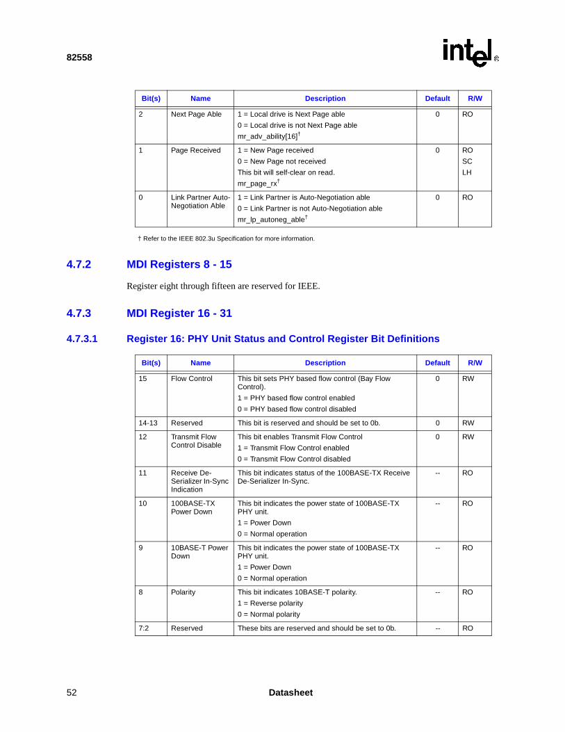
82558
† Refer to the IEEE 802.3u Specification for more information.
4.7.2 MDI Registers 8 - 15
Register eight through fifteen are reserved for IEEE.
4.7.3 MDI Register 16 - 31
4.7.3.1 Register 16: PHY Unit Status and Control Register Bit Definitions
2 Next Page Able 1 = Local drive is Next Page able
0 = Local drive is not Next Page able
mr_adv_ability[16]†
0 RO
1 Page Received 1 = New Page received
0 = New Page not received
This bit will self-clear on read.
mr_page_rx†
0 RO
SC
LH
0 Link Partner Auto-Negotiation Able
1 = Link Partner is Auto-Negotiation able
0 = Link Partner is not Auto-Negotiation able
mr_lp_autoneg_able†
0 RO
Bit(s) Name Description Default R/W
Bit(s) Name Description Default R/W
15 Flow Control This bit sets PHY based flow control (Bay Flow Control).
1 = PHY based flow control enabled
0 = PHY based flow control disabled
0 RW
14-13 Reserved This bit is reserved and should be set to 0b. 0 RW
12 Transmit Flow Control Disable
This bit enables Transmit Flow Control
1 = Transmit Flow Control enabled
0 = Transmit Flow Control disabled
0 RW
11 Receive De-Serializer In-Sync Indication
This bit indicates status of the 100BASE-TX Receive De-Serializer In-Sync.
-- RO
10 100BASE-TX Power Down
This bit indicates the power state of 100BASE-TX PHY unit.
1 = Power Down
0 = Normal operation
-- RO
9 10BASE-T Power Down
This bit indicates the power state of 100BASE-TX PHY unit.
1 = Power Down
0 = Normal operation
-- RO
8 Polarity This bit indicates 10BASE-T polarity.
1 = Reverse polarity
0 = Normal polarity
-- RO
7:2 Reserved These bits are reserved and should be set to 0b. -- RO
52 Datasheet

82558
4.7.3.2 Register 17: PHY Unit Special Control Bit Definitions
1 Speed This bit indicates the Auto-Negotiation result.
1 = 100 Mbps
0 = 10 Mbps
-- RO
0 Duplex Mode This bit indicates the Auto-Negotiation result.
1 = Full Duplex
0 = Half Duplex
-- RO
Bit(s) Name Description Default R/W
15 Scrambler By-pass
1 = By-pass Scrambler
0 = Normal operations
0 RW
14 By-pass 4B/5B 1 = 4 bit to 5 bit by-pass
0 = Normal operation
0 RW
13 Force Transmit H-Pattern
1 = Force transmit H-pattern
0 = Normal operation
0 RW
12 Force 34 Transmit Pattern
1 = Force 34 transmit pattern
0 = Normal operation
0 RW
11 Good Link 1 = 100BASE-TX link good
0 = Normal operation
0 RW
10 Reserved This bit is reserved and should be set to 0b. 0 RW
9 Transmit Carrier Sense Disable
1 = Transmit Carrier Sense disabled
0 = Transmit Carrier Sense enabled
0 RW
8 Disable Dynamic Power Down
1 = Dynamic Power Down disabled
0 = Dynamic Power Down enabled (normal)
0 RW
7 Auto-Negotiation Loopback
1 = Auto-Negotiation loopback
0 = Auto-Negotiation normal mode
0 RW
6 MDI Tri-State 1 = MDI Tri-state (transmit driver tri-states)
0 = Normal operation
0 RW
5 Filter By-pass 1 = By-pass filter
0 = Normal filter operation
0 RW
4 Auto Polarity Disable
1 = Auto Polarity disabled
0 = Normal polarity operation
0 RW
3 Squelch Disable 1 = 10BASE-T squelch test disable
0 = Normal squelch operation
0 RW
2 Extended Squelch
1 = 10BASE-T Extended Squelch control enabled
0 = 10BASE-T Extended Squelch control disabled
0 RW
1 Link Integrity Disable
1 = Link disabled
0 = Normal Link Integrity operation
0 RW
0 Jabber Function Disable
1 = Jabber disabled
0 = Normal Jabber operation
0 RW
Bit(s) Name Description Default R/W
Datasheet 53
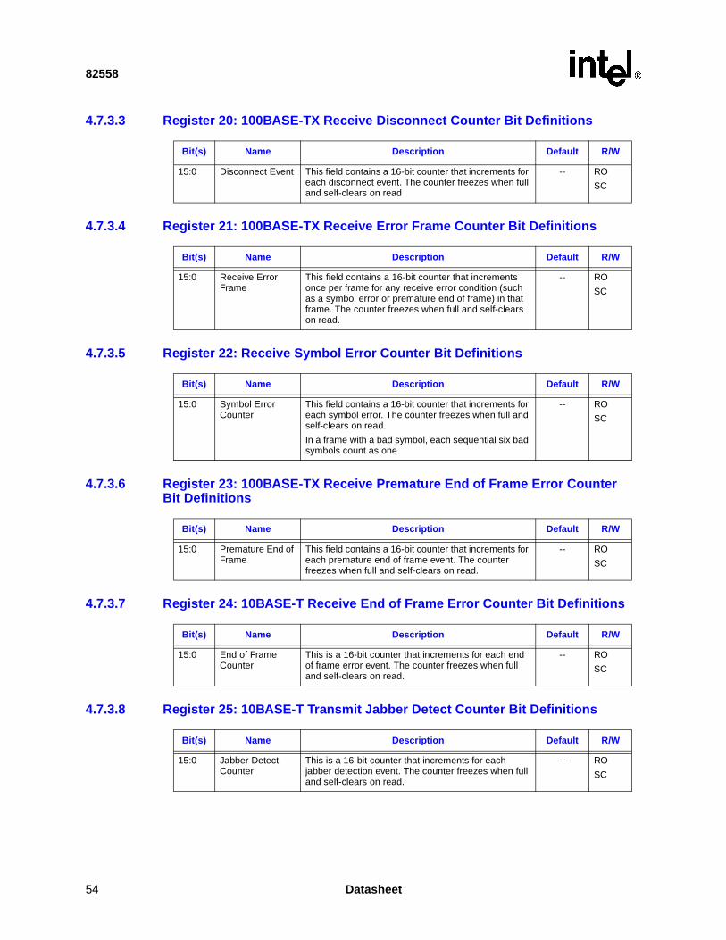
82558
4.7.3.3 Register 20: 100BASE-TX Receive Disconnect Counter Bit Definitions
4.7.3.4 Register 21: 100BASE-TX Receive Error Frame Counter Bit Definitions
4.7.3.5 Register 22: Receive Symbol Error Counter Bit Definitions
4.7.3.6 Register 23: 100BASE-TX Receive Premature End of Frame Error Counter Bit Definitions
4.7.3.7 Register 24: 10BASE-T Receive End of Frame Error Counter Bit Definitions
4.7.3.8 Register 25: 10BASE-T Transmit Jabber Detect Counter Bit Definitions
Bit(s) Name Description Default R/W
15:0 Disconnect Event This field contains a 16-bit counter that increments for each disconnect event. The counter freezes when full and self-clears on read
-- RO
SC
Bit(s) Name Description Default R/W
15:0 Receive Error Frame
This field contains a 16-bit counter that increments once per frame for any receive error condition (such as a symbol error or premature end of frame) in that frame. The counter freezes when full and self-clears on read.
-- RO
SC
Bit(s) Name Description Default R/W
15:0 Symbol Error Counter
This field contains a 16-bit counter that increments for each symbol error. The counter freezes when full and self-clears on read.
In a frame with a bad symbol, each sequential six bad symbols count as one.
-- RO
SC
Bit(s) Name Description Default R/W
15:0 Premature End of Frame
This field contains a 16-bit counter that increments for each premature end of frame event. The counter freezes when full and self-clears on read.
-- RO
SC
Bit(s) Name Description Default R/W
15:0 End of Frame Counter
This is a 16-bit counter that increments for each end of frame error event. The counter freezes when full and self-clears on read.
-- RO
SC
Bit(s) Name Description Default R/W
15:0 Jabber Detect Counter
This is a 16-bit counter that increments for each jabber detection event. The counter freezes when full and self-clears on read.
-- RO
SC
54 Datasheet
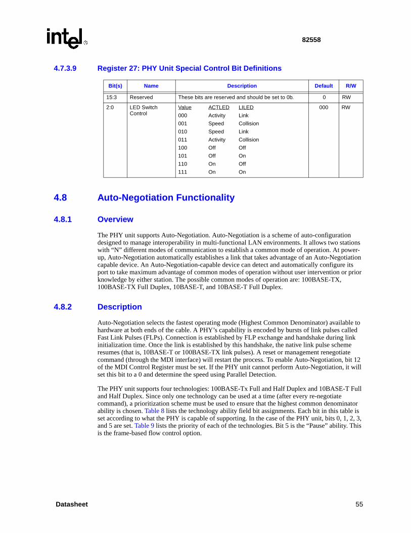
82558
ons er-
iation its prior
ble to lled link e
te it 12 will
Full
inator is , 2, 3, is
4.7.3.9 Register 27: PHY Unit Special Control Bit Definitions
4.8 Auto-Negotiation Functionality
4.8.1 Overview
The PHY unit supports Auto-Negotiation. Auto-Negotiation is a scheme of auto-configurationdesigned to manage interoperability in multi-functional LAN environments. It allows two statiwith “N” different modes of communication to establish a common mode of operation. At powup, Auto-Negotiation automatically establishes a link that takes advantage of an Auto-Negotcapable device. An Auto-Negotiation-capable device can detect and automatically configureport to take maximum advantage of common modes of operation without user intervention orknowledge by either station. The possible common modes of operation are: 100BASE-TX, 100BASE-TX Full Duplex, 10BASE-T, and 10BASE-T Full Duplex.
4.8.2 Description
Auto-Negotiation selects the fastest operating mode (Highest Common Denominator) availahardware at both ends of the cable. A PHY’s capability is encoded by bursts of link pulses caFast Link Pulses (FLPs). Connection is established by FLP exchange and handshake duringinitialization time. Once the link is established by this handshake, the native link pulse schemresumes (that is, 10BASE-T or 100BASE-TX link pulses). A reset or management renegotiacommand (through the MDI interface) will restart the process. To enable Auto-Negotiation, bof the MDI Control Register must be set. If the PHY unit cannot perform Auto-Negotiation, it set this bit to a 0 and determine the speed using Parallel Detection.
The PHY unit supports four technologies: 100BASE-Tx Full and Half Duplex and 10BASE-T and Half Duplex. Since only one technology can be used at a time (after every re-negotiate command), a prioritization scheme must be used to ensure that the highest common denomability is chosen. Table 8 lists the technology ability field bit assignments. Each bit in this table set according to what the PHY is capable of supporting. In the case of the PHY unit, bits 0, 1and 5 are set. Table 9 lists the priority of each of the technologies. Bit 5 is the “Pause” ability. This the frame-based flow control option.
Bit(s) Name Description Default R/W
15:3 Reserved These bits are reserved and should be set to 0b. 0 RW
2:0 LED Switch Control
Value
000
001
010
011
100
101
110
111
ACTLED
Activity
Speed
Speed
Activity
Off
Off
On
On
LILED
Link
Collision
Link
Collision
Off
On
Off
On
000 RW
Datasheet 55
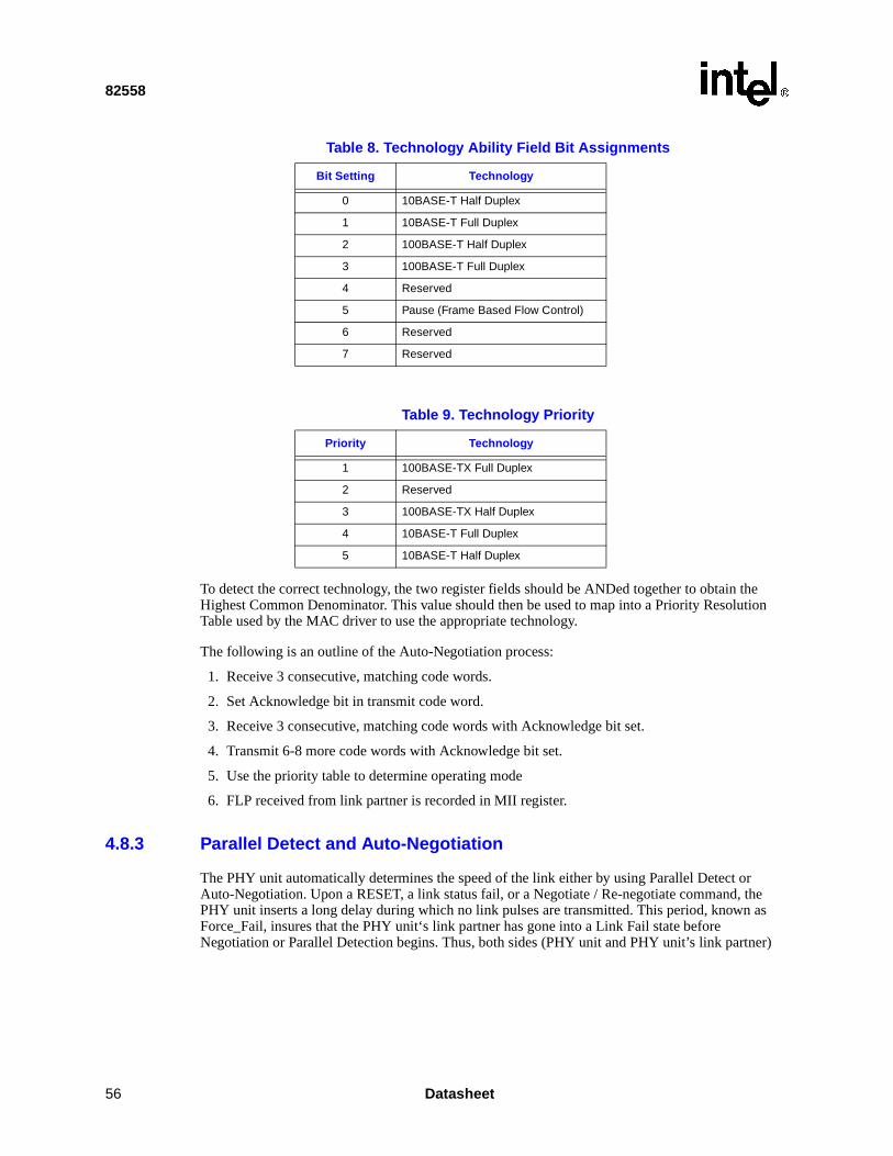
82558
the tion
r the as
ner)
To detect the correct technology, the two register fields should be ANDed together to obtain Highest Common Denominator. This value should then be used to map into a Priority ResoluTable used by the MAC driver to use the appropriate technology.
The following is an outline of the Auto-Negotiation process:
1. Receive 3 consecutive, matching code words.
2. Set Acknowledge bit in transmit code word.
3. Receive 3 consecutive, matching code words with Acknowledge bit set.
4. Transmit 6-8 more code words with Acknowledge bit set.
5. Use the priority table to determine operating mode
6. FLP received from link partner is recorded in MII register.
4.8.3 Parallel Detect and Auto-Negotiation
The PHY unit automatically determines the speed of the link either by using Parallel Detect oAuto-Negotiation. Upon a RESET, a link status fail, or a Negotiate / Re-negotiate command,PHY unit inserts a long delay during which no link pulses are transmitted. This period, knownForce_Fail, insures that the PHY unit‘s link partner has gone into a Link Fail state before Negotiation or Parallel Detection begins. Thus, both sides (PHY unit and PHY unit’s link part
Table 8. Technology Ability Field Bit Assignments
Bit Setting Technology
0 10BASE-T Half Duplex
1 10BASE-T Full Duplex
2 100BASE-T Half Duplex
3 100BASE-T Full Duplex
4 Reserved
5 Pause (Frame Based Flow Control)
6 Reserved
7 Reserved
Table 9. Technology Priority
Priority Technology
1 100BASE-TX Full Duplex
2 Reserved
3 100BASE-TX Half Duplex
4 10BASE-T Full Duplex
5 10BASE-T Half Duplex
56 Datasheet

82558
will
eed.
een
a ast s.
8 is
will perform Auto-Negotiation or Parallel Detection with no data packets being transmitted. Connection is then established either by FLP exchange or Parallel Detection. The PHY unit look for both FLPs and link integrity pulses. The following diagram illustrates this process.
4.9 LED Description
The PHY unit supports three LED pins to indicate link status, network activity and network sp
LINK (LINK_N) : This LED is OFF until a valid link has been detected. After a valid link has bdetected, the LED will remain ON (active-low).
ACTIVITY (ACT_N) : This LED is ON (active-low) when activity is detected on the wire.
SPEED (SPEED_N): This LED will be ON if a 100BASE-TX link is detected and OFF in case10BASE-T link is detected. In case link fails while in Auto-Negotiation, this LED will keep the lvalid link state. If 100BASE-TX link is forced this LED will be ON, regardless of the link statuThis LED will be OFF in case 10BASE-T link is forced, regardless of the link status.
See MDI register 27 for LED function mapping support enhancements.
4.10 Power Management
Note: Section 4.10.1 through Section 4.10.6 refer to power management implementations of the 8255A-step. The 82558 B-step implements power management in a slightly different manner and
Figure 22. Auto-Negotiation and Parallel Detect
Force_Fail
Ability detect either byparallel detect or auto-
negotiation.
10Base-T or100Base-TX Link
ReadyFLP capable
LINK PASS
Parallel Detection Auto-Negotiation
Look at Link Pulse;Auto-Negotiation capable = 0
Auto-Negotiation capable = 1Ability Match
Auto-Negotiation Complete bit set
Datasheet 57
82558
p” on
ket. As
ddress
o by
ware to he PCI tting
fy as a heres
sms
16
nce it d in the ). The
M
has sertion
described in Section 4.10.7, “Power Management Feature Enhancements for the 82558 B-stepage 64.
4.10.1 Wake-up Packet
The 82558 can wake up the system when it receives a frame that qualifies as a wake-up pacmentioned, this packet can be configured to be one or both of the following:
• Any frame destined to the 82558 such as a frame that matches one of the 82558 active afiltering mechanisms (unique Individual Address, Broadcast, Multicast, Promiscuous).
• Magic Packet* (see Section 4.10.1.1).
The 82558 notifies the system about the reception of a wake-up packet, if configured to do ssetting the PME_Enable bit in the PMCSR. The 82558 determines which of these two frameformats to use according to a configuration bit in the 82558 standard Configure command.
If configured to do so, the 82558 notifies the system whenever a qualified wake-up packet isreceived regardless of whether the 82558 is in the D1 state or the D0 state. It is up to the softensure that the PME_Enable bit is set only when the 82558 is in the D1 state as required by tPower Management Specification. The 82558 notifies the system by asserting PME# and sethe PME status bit in the PMCSR and CSR.
4.10.1.1 Magic Packet*
When the 82558 is configured to Magic Packet mode, it requires that a received packet qualiMagic Packet*, after which it generates a wake-up signal. A Magic Packet* is a packet that adto the following rules:
1. Has a valid Destination Address that passes one of the 82558 address filtering mechani
2. Has a valid CRC
3. Includes, anywhere in the packet, an uninterrupted sequence of 6 FFh bytes followed byduplications of the 82558 individual address.
The 82558 scans for the sequence of 16 repetitions of its IA. If the 82558 detects this sequeasserts a Power Management Event (PME). The event asserts the PME# pin and is reflectePower Management Control/Status Register (PMCSR) and the Control/Status Register (CSR82558 does not pass the Magic Packet to system memory.
4.10.2 Wake on LAN* (WOL) Mode
The 82558 supports a special Wake on LAN (WOL) mode. In this mode, the 82558:
• Automatically enters WOL mode after hardware reset
The 82558 will scan for Magic Packet and assert PME# when it has been detected.
• Can be set into low power mode via a disable/low power pin on the 82558 A-step only
• Changes the functionality of the Activity LED
WOL mode is enabled automatically after the 82558 detects that the WOL bit in the EEPRO(word Ah, bit 5) has been set. The 82558 continues to read the EEPROM, including the six individual address bytes from word addresses 0h through 2h. When the EEPROM read has completed, the 82558 begins scanning for a Magic Packet (although no Configure commandbeen issued). If a Magic Packet is detected, the 82558 asserts PME#. In WOL mode, the asof PME# is not gated by PCI Power Management registers (PME Enable bit).
58 Datasheet
82558
ode that
ode).
ovides
such
ndards
ber
ision
cted kes one n the
ny does eceive
nt.
wered o by
IA) in e on
While in WOL mode, the PCI portion of the 82558 is expected to be non-functional. The ISOLATE# signal should be asserted if the PCI bus is not valid
For the 82558 A-step, if the WOL bit in the EEPROM is set, the FLD4 pin functions as a low power pin. When this pin is asserted (high), it places the PHY and CSMA units in low power m(D3 state). In order to achieve a full “power down” the ISOLATE# pin should be asserted. Notethis disables the ability to use the Flash interface in WOL mode system.
If the WOL bit is set in the EEPROM, the functionality of the Activity LED is modified. It indicates that a received frame passed CSMA/CD address filtering (excluding promiscuous m
4.10.3 Low Power Mode Requirements
The 82558 provides support for system level Low Power Modes. To enable this, the 82558 prthe following capabilities:
1. The 82558 can monitor the network for a “Wake-up Packet” and notify the system whena packet arrives.
2. The 82558 A-step can be set in a Power-Off mode in which it consumes only 250 mW.
3. The 82558 has the ability to isolate itself from the PCI bus.
These three capabilities enable the 82558 to adhere to the emerging power management staas defined in:
• PCI Bus Power Management Interface Specification, Revision 1.0, January 6, 1997.
• Advanced Configuration and Power Interface Specification (ACPI), Revision 1.0, Decem22, 1996.
• Device Class Power Management Reference Specification - Network Device Class, Rev1.0.
These three specifications define how a PCI network device can be controlled in an OS DirePower Management (OSPM) environment. The 82558 adheres to these specifications and tastep further to support bus isolation within the chip when it is in a low power mode. Details odifferent power modes are provided in Table 10 “Power States” on page 60.
The 82558 does not transmit any frames during any Low Power Mode, nor does it process aother Control or Action Commands. When in the D1 through D3 low power modes, the 82558not pass any received frames to system memory; however, it does maintain the capability to rframes for wake-up purposes as mentioned in Section 4.10.1, “Wake-up Packet” on page 58.
When in the D1 through D3 low power modes, the 82558 assumes that a stable link is prese
Unless the 82558 is in WOL mode, after reset (power up reset included) the 82558 is fully poup. The 82558 does not enter low power mode nor filter for wake-up packets until set to do ssoftware. The 82558 requires that its driver be loaded prior to its being set into any of the lowpower modes. The driver needs to perform some initialization functions (such as setting the order for the 82558 to operate properly in the low power modes. The exception to this is WakLAN (WOL) mode. More details are on Wake on LAN mode are provided in Section 4.10.2, “Wake on LAN* (WOL) Mode” on page 58.
Datasheet 59

82558
s o D0 pects k is smit
is to
ed 82558
cted
tes in
is aces.
4.10.4 82558 Device Power States
The 82558 supports the following power states:
4.10.4.1 D0 State - Full Power
The D0 state is the normal operation state of the 82558. In this state the device consumes itnominal power (<2.5 W) and is capable of transmitting and receiving. The 82558 defaults intstate after any hardware reset, including power-on reset. While in the D0, state the 82558 exthe PCI clock to be continuously operating at any frequency above 12.5 MHz. If the PCI clocstopped or slowed to any frequency lower than 12.5 MHz, the 82558 may not receive or tranframes properly.
4.10.4.2 D1 to D3 States - Monitor for Wake-up Packet
The D1 state of the 82558 does not differ from the D0 state. However, the intent of this statehave the 82558 operate in the following conditions:
• The driver is not initiating any control or action commands to the 82558. It is recommendthat the RU and CU be in the Idle/Suspended state prior to setting the 82558 to D1. The does not guarantee proper transmission or reception of frames in the D1 state.
• The PCI clock can be running at any frequency from 33 MHz down to DC.
• The 82558 may be instructed to monitor for wake-up frames. When such a frame is detethe 82558 asserts a PME# to the system.
The 82558 consumes no more than 2.5 W of power when operating in the D1 through D3 stathe above mentioned conditions.
The 82558 can be accessed as a slave in configuration space only, as long as the PCI clockrunning. The 82558 does not respond to Memory and I/O accesses to its various address sp
Table 10. Power States
82558 Device States
PCI Bus
States
Function Context
Clock Frequency Power
Supported Actions to Function
Supported Actions from
Function
D0 B0 Full function context in place
Full speed Full power Any PCI transaction
Any PCI transaction or interrupt
D1 B0 or B1
Configuration maintained; no transmit or receive except wake-up packets
Stopped to full speed
≤ 2.5 W PCI configuration access
Wake-up event
D2 B0 or B1
Configuration maintained; no transmit or receive
Stopped to full speed
≤ 250 mW if clock stopped
PCI configuration access
D3 B0 or B1
Configuration lost; initialization required upon return to D0
Stopped to full speed
≤ 250 mW if clock stopped
PCI configuration access
D3 B3 All configuration lost; power-on defaults in place on return to D0
No clock No power Power-up reset only
60 Datasheet
82558
ional the PCI terrupt.
l reset ower tion
to D0 rted by e D1 ll PCI
he smit
. its a
The
l
atting e,
When in the D1 through D3 states, all the 82558 units (PHY, CSMA and Parallel) are operatand will operate as long as they get a clock. However, the 82558 does not attempt to access bus when in the D1 to D3 states and does not generate interrupts, other than the wake-up in
4.10.4.3 D3 State - Power Off State
When the 82558 is instructed to return to the D0 state from the D3 state it initiates an internawhich resets all its internal registers, including PCI configuration registers but excluding the PManagement block. The 82558 requires a full PCI initialization sequence and driver initializasequence before it can be properly used.
Note: The D2 and D3 states of the 82558 are practically identical except for the reset when restoredstate. The D3 state is required to meet upcoming industry standards. The D2 state is suppothe 82558 in order to enable stopping of the PCI clock in the system (which is prohibited in thstate although the 82558 can accommodate it) without forcing the system to go through the fuinitialization sequence.
4.10.5 Link Operation
During D1 state, the 82558 maintains an active link. This implies the following.
• PHYTX 10 Mbps mode: The 82558 expects to get normal clock input on the X1 X2 pins. T82558 expects to receive normal reception on the RDP/RDN pair. The 82558 will not tranon the TDP/TDN pair.
• PHYTX 100 Mbps mode: The 82558 expects to get normal clock input on the X1 X2 pinsThe 82558 expects to receive normal reception on the RDP/RDN pair. The 82558 transmcontinuous Idle stream on the TDP/TDN pair, as required by the 100BASE-TX standard.82558 does not transmit frames on the link.
• Auto-Negotiation: If the link fails while the 82558 is in the D1 state, it performs the normaAuto-negotiation protocol in order to re-establish the link.
In the three “linked” cases, any frame received is processed by the 82558 for valid frame formand address filtering. No frame is guaranteed to be passed to system memory in the D1 statincluding a frame that qualifies as a wake-up frame.
During D2 and D3 states the 82558 does not maintain an active link.
4.10.6 Power Management Registers
The 82558 has four power management registers:
1. Power Management Capability Pointer - Cap_Ptr.
2. Power Management Capabilities - PMC.
3. Power Management Control/Status - PMCSR.
4. Power Management Driver Register - PMDR.
Datasheet 61

82558
register
gister
is
y list. Ptr is
4.10.6.1 Power Management Pointer - Cap_Ptr
The Power Management Pointer Register describes the location of the power management block. The value of this pointer in the 82558 is DCh as recommended in the PCI Power Management Specification.
The location of the Cap_Ptr is at offset 34h in the PCI configuration space.
If the power management bit is not set in the EEPROM, it forces the value of the Cap_Ptr reto ‘0’.
4.10.6.2 Capability Identifier - Cap_ID
The Capability Identifier signals that this item in the linked list is the registers defined for PCI Power Management. PCI Power Management has been assigned the ID of 01h. The Cap_IDlocated in the 82558 PCI configuration space at offset 01h.
4.10.6.3 Next Item Pointer - Next_Item_Ptr
The Next Item Pointer Register describes the location of the next item in the 82558 capabilitSince power management is the last item in the list, this register is set to 0. The Next_Item_located in the 82558 PCI configuration space at offset 00h.
Table 11. Power Management Pointer - Cap_Ptr
Bits Value Read/Write Description
7:0 DCh Read Only Cap_Ptr . This field provides an offset into the 82558 PCI Configuration Space pointing to the location of the Power Management Control and Status Registers. A value of ‘0’ means that this function does not implement the power management register block. The 82558 has this field set to ‘0’ if the PM bit is not set in the EEPROM.
Table 12. Capability Identifier - Cap_ID
Bits Value Read/Write Description
7:0 01h Read Only Cap_ID. This field identifies the linked list item as being the PCI Power Management Registers. It is set to 01h which is the value that has been assigned by the PCI SIG for Power Management capability.
Table 13. Next Item Pointer - Next_Item_Ptr
Bits Value Read/Write Description
7:0 00h Read Only Next Item Pointer . This field provides an offset into the function’s PCI Configuration Space pointing to the location of the next item in the function’s capability list. This field is set to ‘0’ in the 82558.
62 Datasheet

82558
is in the
s for the
4.10.6.4 Power Management Capabilities - PMC
The Power Management Capabilities register is a 16 bit read-only register which provides information on the capabilities of the 82558 related to power management. The Version fieldused to tell the software how to interpret the PMC and PMCSR registers. This field is set to 182558. The PMC is located in the 82558 PCI configuration space at offset DEh.
4.10.6.5 Power Management Control and Status Register - PMCSR
This register is used to determine and change the current power state of the 82558 and allowthe control of the power management interrupts in a standard way. The PMCSR is located in82558 PCI configuration space at offset E0h.
Table 14. Power Management Capabilities - PMC
Bits Value Read/Write Description
31:27 00011 Read Only PME_Support . This five bit field indicates the power states in which the D101 may assert PME#. A value of ‘0’ for any bit indicates that the function is not capable of asserting the PME# signal while in that power state. The 82558 supports wake-up from the D0 and D1 power states.
26 1 Read Only D2_Support . If this bit is set, this function supports the D2 power state. All devices must support the D0 and D3 states; however, the 82558 also supports the D2 state.
25 1 Read Only D1_Support . If this bit is set this function supports the D1 power state. All devices must support the D0 and D3 states; however, the 82558 also supports the D1 power state.
24:22 000 Read Only Reserved . These bits are reserved and should be set to 000b.
21 1 Read Only Device Specific Initialization (DSI). The DSI bit indicates whether special initialization of this function is required (beyond the standard PCI configuration header) before the generic class device driver is able to use it. DSI is required for the 82558 after the D3-to-D0 reset.
20 0 Read Only Auxiliary Power Source . This bit is only meaningful if the Power Management Control and Status Register (PMCSR) bit 31 is ‘1’. When this bit is set to ‘1’, it indicates that support for PME# in D3cold requires auxiliary power supplied by the system. The 82558 returns a ‘0’ in bit 31, which makes this bit meaningless.
19 0 Read Only PME Clock . When this bit is a 1, it indicates that the function’s PME# generation logic requires its host PCI bus to maintain a free running PCI clock. When this bit is a “0” it indicates that no host bus clock is required for the function to generate PME#. The 82558 does not require a clock to generate PME# so it returns 0.
18:16 001 Read Only Version . A value of 001b indicates that the 82558 complies with the Revision 1.0 of the PCI Power Management Interface Specification.
Table 15. Power Management Control and Status Register - PMCSR
Bits Value Read/Write Description
15 0 Read/Clear PME Status . This bit is set upon a wake-up event from the link. It is independent of the state of the PME_Enable bit. When software writes a ‘1’ to this bit, it is cleared and the 82558 stops asserting PME# (if enabled).
14:13 00 Read Only Data Scale . This is not supported at this time and always returns 00b.
12:9 0000 Read Only Data Select . This is not supported at this time and always returns a 0000b.
Datasheet 63
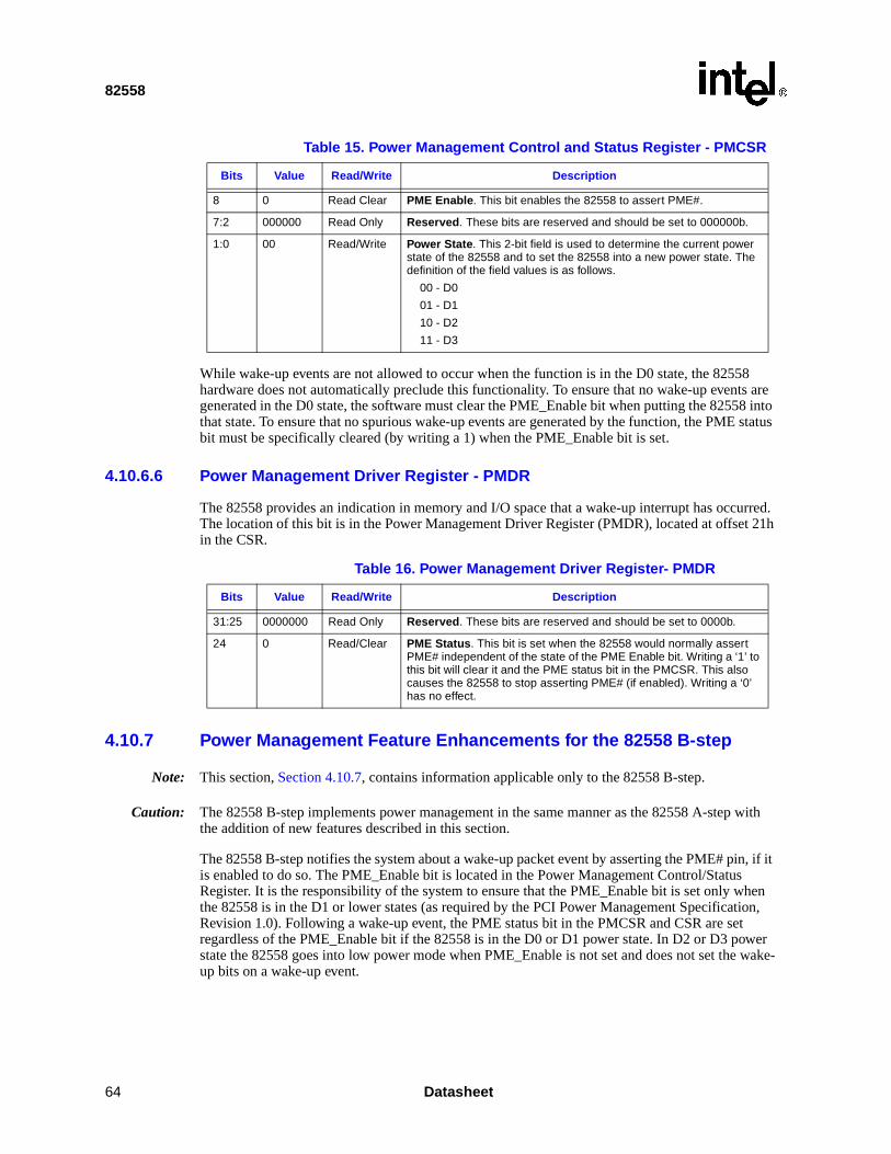
82558
8 ts are 58 into E status
urred. t 21h
with
in, if it s hen
tion, t wer
e wake-
While wake-up events are not allowed to occur when the function is in the D0 state, the 8255hardware does not automatically preclude this functionality. To ensure that no wake-up evengenerated in the D0 state, the software must clear the PME_Enable bit when putting the 825that state. To ensure that no spurious wake-up events are generated by the function, the PMbit must be specifically cleared (by writing a 1) when the PME_Enable bit is set.
4.10.6.6 Power Management Driver Register - PMDR
The 82558 provides an indication in memory and I/O space that a wake-up interrupt has occThe location of this bit is in the Power Management Driver Register (PMDR), located at offsein the CSR.
4.10.7 Power Management Feature Enhancements for the 82558 B-step
Note: This section, Section 4.10.7, contains information applicable only to the 82558 B-step.
Caution: The 82558 B-step implements power management in the same manner as the 82558 A-stepthe addition of new features described in this section.
The 82558 B-step notifies the system about a wake-up packet event by asserting the PME# pis enabled to do so. The PME_Enable bit is located in the Power Management Control/StatuRegister. It is the responsibility of the system to ensure that the PME_Enable bit is set only wthe 82558 is in the D1 or lower states (as required by the PCI Power Management SpecificaRevision 1.0). Following a wake-up event, the PME status bit in the PMCSR and CSR are seregardless of the PME_Enable bit if the 82558 is in the D0 or D1 power state. In D2 or D3 postate the 82558 goes into low power mode when PME_Enable is not set and does not set thup bits on a wake-up event.
8 0 Read Clear PME Enable . This bit enables the 82558 to assert PME#.
7:2 000000 Read Only Reserved . These bits are reserved and should be set to 000000b.
1:0 00 Read/Write Power State . This 2-bit field is used to determine the current power state of the 82558 and to set the 82558 into a new power state. The definition of the field values is as follows.
00 - D0
01 - D1
10 - D2
11 - D3
Table 15. Power Management Control and Status Register - PMCSR
Bits Value Read/Write Description
Table 16. Power Management Driver Register- PMDR
Bits Value Read/Write Description
31:25 0000000 Read Only Reserved . These bits are reserved and should be set to 0000b.
24 0 Read/Clear PME Status . This bit is set when the 82558 would normally assert PME# independent of the state of the PME Enable bit. Writing a ‘1’ to this bit will clear it and the PME status bit in the PMCSR. This also causes the 82558 to stop asserting PME# (if enabled). Writing a ‘0’ has no effect.
64 Datasheet

82558
t. The ed
ability his
and
the ATE#
er. If 3
filters rnal
558 units e D1
There are two types of wake-up events: reception of a wake up packet and a link status evendetection mechanism of the wake up packets (packet filtering) is further categorized upon fixpacket filtering implemented by hardware and flexible packet filtering implemented by the loadable microcode.
4.10.7.1 Wake-up Capabilities
4.10.7.1.1 Wake-up Indication in the Power Management Registers
The 82558 uses two different mechanisms to wake up the system:
• Directed, Multicast, Magic Packet, and VLAN Wake-up
This is implemented in hardware by using the clock driven on the X1 pin.
• Flexible Filtering
This is implemented in loadable microcode, using PCI CLK pin as clock.
The 82558 B-step is able to generate a wake-up event if power is supplied to the device. Theto use loadable microcode for frame filtering requires a valid clock on the PCI CLK pin. For tfeature, the 82558 may be configured so it will not isolate the CLK pin when ISOLATE# is asserted.
The following table describes wake-up capabilities in different combinations of power supplyclock:
Note: If an external clock circuit is implemented and functional in D3, the Clock Isolate Disable bit inEEPROM should be set to enable CLK propagation to the 82558 B-step core while the ISOLsignal is asserted.
The 82558 B-step samples the LISTAT pin after reset to determine status of the auxiliary powthis pin is pulled low, the 82558 B-step assumes that auxiliary power will be supplied in the Dcold state. Section 4.10.7.1.3, “Auxiliary Power Indication” on page 66 provides more details.
The 82558 B-step cannot determine whether or not an external clock circuit exists. Since all implemented in the hardware do not required a clock signal on the CLK pin (pin 35), the exteclock circuit has no affect on the reporting of wake-up capabilities.
4.10.7.1.2 Low Power Modes
The 82558 B-step wake-up capabilities require all internal blocks to fully active. When the 82B-step is in the D2 or D3 power states and wake-up is disabled, the internal PHY and CSMAare set into low power modes. In this mode the 82558 B-step loses the link connection. In thpower state, the PHY and CSMA units are operational.
Table 17. Wake-up Capabilities
Ext Clock Circuit
Aux Power Present
Directed, Multicast, Magic Packet, and
ARP Wake-up
Flexible Filtering Wake-up PME Support in PMC
No No D1, D2, D3hot D1 01111b
No Yes D1, D2, D3hot, D3cold D1 11111b
Yes No D1, D2, D3hot D1, D2, D3hot 01111b
Yes Yes D1, D2, D3hot, D3cold D1, D1, D3hot, D3cold 11111b
Datasheet 65

82558
and 82558
wer
this from
Note that if the 82558 B-step is set into a low power mode (such as D2 or D3) with the PME_Enable bit cleared, it will immediately turn off the internal PHY unit. Setting the PME_Enable bit while the 82558 B-step is in a low power state will power up the internal PHYestablish link connection. If the wake-up on the Link Status Change feature is enabled in the configuration, the 82558 B-Step will wake up the system. To avoid the above scenario, the PME_Enable bit should be enabled before the 82558 is set into low power mode.
Note: Information regarding clock isolation in low power states can be obtained in AP-386, “Low PoMode Clocking Considerations.”
4.10.7.1.3 Auxiliary Power Indication
The 82558 B-step supports wake up from D3cold if an auxiliary power supply exists in this power state. The LISTAT pin (pin 204) is used to indicate the existence of an AUX power supply. If pin is 0 after reset, the 82558 B-step will enable wake-up capability from D3. If this bit is 1 orfloating (not connected), the 82558 B-step will assume no auxiliary power exist and wake upD3 will be disabled.
4.10.7.2 82558 B-step Power Management Configuration Registers
4.10.7.2.1 Power Management Capabilities (PMC)
Table 18. 82558 B-step Power Management Capabilities - PMC
Bits Value Read/Write Description
31:27 00011(no auxiliary power)
11111(auxiliary power)
Read Only PME_Support . This five bit field indicates the power states in which the 82558 may assert PME#. A value of 0 for any bit indicates that the function is not capable of asserting the PME# signal while in that power state. The 82558 B-step supports wake-up from D0, D1, D2, and D3hot if no auxiliary power supply is present. The 82558 B-step also supports all power states if an auxiliary power supply is present. The LISTAT pin (pin 204) is used as an auxiliary power signal (AUX)to the 82558 B-step. If it is pulled high, no auxiliary power is present. Thus, if it is pulled low, an auxiliary power supply is present.
26 1 Read Only D2_Support . If this bit is set, this function supports the D2 power state. All devices must support the D0 and D3 states; however, the 82558 also supports the D2 state.
25 1 Read Only D1_Support . If this bit is set this function supports the D1 power state. All devices must support the D0 and D3 states; however, the 82558 also supports the D1 power state.
24:22 000 Read Only Reserved . These bits are reserved and should be set to 000b.
21 1 Read Only Device Specific Initialization (DSI). The DSI bit indicates whether special initialization of this function is required (beyond the standard PCI configuration header) before the generic class device driver is able to use it. DSI is required for the 82558 after the D3-to-D0 reset.
20 0 Read Only Auxiliary Power Source . This bit is only meaningful if the Power Management Control and Status Register (PMCSR) bit 31 is ‘1’. When this bit is set to ‘1’, it indicates that support for PME# in D3cold requires auxiliary power supplied by the system. The 82558 returns a ‘0’ in bit 31, which makes this bit meaningless.
19 0 Read Only PME Clock . When this bit is a 1, it indicates that the function’s PME# generation logic requires its host PCI bus to maintain a free running PCI clock. When this bit is a “0” it indicates that no host bus clock is required for the function to generate PME#. The 82558 does not require a clock to generate PME# so it returns 0.
66 Datasheet

82558
its in
ed e
e-up the s ese
Note: The shaded area defines the difference in the 82558 B-step from the 82558 A-step.
4.10.7.2.2 Power Management Control and Status Register (PMCSR)
Note: The shaded areas define the differences in the 82558 B-step from the 82558 A-step.
4.10.7.3 Power Management Event Context After Reset
The PCI Power Management specification requires that the PME_Status and PME_Enable bPMCSR will not be cleared by PCI RST# if the function supports wake up from a D3cold state. If the 82558 samples LISTAT low after reset, it will assume that an auxiliary power source is usand wake up from the D3cold state is possible. In this case assertion of RST# will not clear thesbits.
In order to support WOL mode (preboot wake-up) the 82558 should be able to generate wakevents without any software configuration, including PCI PM configuration. For this purpose PME_Enable default value after power-up reset is ‘1', wake-up enabled, and the PME_Statudefault value after power-up reset is ‘0'. Since the OS and BIOS expect unknown values in th
18:16 001 Read Only Version . A value of 001b indicates that the 82558 complies with the Revision 1.0 of the PCI Power Management Interface Specification.
Table 18. 82558 B-step Power Management Capabilities - PMC
Bits Value Read/Write Description
Table 19. 82558 B-step Power Management Control and Status Register - PMCSR
Bits Value Read/Write Description
15 If no auxiliary power is present, this value is unknown.
Read/Clear PME Status . This bit is set upon a wake-up event from the link. It is independent of the state of the PME_Enable bit. When software writes a ‘1’ to this bit, it is cleared and the 82558, if enabled, stops asserting PME#.
The LISTAT pin can be used to determine if auxiliary power is present or not.
14:13 00 Read Only Data Scale . This is not supported at this time and always returns 00b.
12:9 0000 Read Only Data Select . This is not supported at this time and always returns a 0000b.
8 If no auxiliary power is present, this value is unknown.
Read/Clear PME Enable . This bit enables the 82558 to assert PME#.
The LISTAT pin can be used to determine if auxiliary power is present or not.
7:2 000000 Read Only Reserved . These bits are reserved and should be set to 000000b.
1:0 00 Read/Write Power State . This 2-bit field is used to determine the current power state of the 82558 and to set the 82558 into a new power state. The definition of the field values is as follows.
00 - D0
01 - D1
10 - D2
11 - D3
Datasheet 67

82558
ode r
e it is
es in
RST# al to
and
are
, r all hich
al for ering on
rred to ing
is
.
bits after power-up, they will clear both bits using the PCI configuration command. If WOL mis enabled, the 82558 B-step will wake up the system upon detection of a Magic Packet aftepower-up without the need for software interaction.
If wake-up from D3cold is not supported, both the PME_Enable and PME_Status bits should binactive, 0b, after reset. In order to enable WOL functionality in this case, the PME_Enable bignored if the WOL mode is enabled and the auxiliary power indication is not active.
The table below summarizes PME_Enable and PME_Status bits default values and propertivarious configurations:
PME_Enable and PME_Status are set to their default values after a power-up reset. The ALTis used as a power-up reset signal and should be connected to the auxiliary-power-valid signensure an active low on system power-up. Assertion of ALTRST# clears the PME_Status bitsets the PME_Enable bit.
If the system does not support auxiliary power and the WOL bit in EEPROM is set, the PME_Enable bit is ignored by the 82558 B-step. In this case PME_Enable and PME_Statusboth cleared to '0' by the PCI RST# signal, as required by the PCI Power Management specification. Note that in this configuration (WOL bit set without auxiliary power) the PME enable bit is always ignored regardless of the wake-up event type.
4.10.7.4 Fixed Packet Filtering
Fixed packet filtering includes the wake-up capabilities implemented in the hardware with a predefined fixed pattern. The fixed patterns include: Address Match (Directed and Multicast)Magic Packets*, and Address Resolution Protocol (ARP) Packets. The 82558 B-step will filteincoming frames, monitoring for one of the packet types mentioned previously, regardless of wpower state it is in. Each fixed filter can be enabled using the 82558 B-step Configuration command. When the PME_Enable bit is enabled the 82558 B-step will assert the PME# signframes that have been filtered through and that contains correct value in its CRC field. This filtmechanism is active whenever power is supplied to the device with or without an active clockthe PCI bus.
Regardless of the PME configuration, packets that pass through address filtering are transfethe internal Micromachine. The Micromachine may store and analyze the packet if the followconditions are met:
• The loadable microcode to analyze and store the packet in the Micromachine resourcesactive.
• The clock signal is active on PCI CLK pin.
• The external clock switching circuit used during the B2 and B3 PCI bus states is present
Table 20. PME Enable and PME Status Bits Properties
Aux Power (indicated by LISTAT)
WOL Bit (EEPROM)
PME Enable (default)
PME Status (default)
RST# clears bits?
PME Enable by-passed upon wake-
up event?
No 0 0 0 Yes No
No 1 0 0 Yes Yes
Yes X 1 0 No No
68 Datasheet

82558
ress
and
ke up bit in byte
xible
by the
e acket
4.10.7.4.1 Address Matching
The 82558 B-step may be configured to wake up the system on any packet that passes the Individual Address filtering or the Multicast Address filtering. The wake-up enable status is defined by the IA Match Wake Enable bit and Multicast Match Wake Enable bit in the configuration structure. The following modifications for the 82558 B-step in relation to the addmatching filters:
• Address match wake-up depends on two configuration bits:
— IA Match Wake Enable: Byte 19, bit 0 in the configuration command.
— Multicast Match Wake enable: Byte 9, bit 7 in the configuration command.
• Broadcast address match in the 82558 B-step will not wake up a system (except for ARPflexible filtering frames).
4.10.7.4.2 Address Resolution Protocol (ARP)
Address Resolution Protocol (ARP) is used for MAC address resolution of a machine. This protocol generally precedes any Internet Protocol (IP) transaction. The 82558 B-step can wathe system when an ARP frame is received if it is configured to do so by the ARP_Wake_Enthe configuration command. In order for ARP filtering to function, the Broadcast Disable bit (15, bit 1) should be set to zero (broadcast enabled).
The 82558 B-step can handle Virtual LAN (VLAN) headers if it is configured to do so by the VLAN_ARP bit in the configuration command (byte 9, bit 4).
Fixed packet filtering does not have the ability to support multiple IP addresses; however, flefiltering does.
4.10.7.5 Flexible Packet Filtering
Programmable packet filtering is targeted to support wake-up packets that are not supportedhardware filters. Known wake-up packets include the following.
Wake-up packets supported by the 82558 B-step hardware filters are: ARP packets (Ethernet II packet with single IP address filtering)
• Directed packet
• Multicast address packet
• Magic Packet
• Link event
Wake-up packets that are not supported by the 82558 B-step filters are:
• Directed IP packet
• NetBIOS queries
• 802.2 ARP packets
• Multiple IP address recognition
Flexible Packet Filtering is supported via loadable microcode. The microcode should be programmed by the driver before the 82558 B-step is set into low power mode. Thus, FlexiblPacket Filtering is beyond the scope of this document. More details on the 82558's Flexible PFiltering capabilities can be found in the 82558 Software Developer's Manual.
Datasheet 69

82558
ignal if tion ect or tus or
4.10.7.6 Link Status Event
Link disconnect and connect should be treated as link status events and generate a PME# sthe PME_Enable bit is enabled. The Link Status Wake Enable bit was added to the configuracommand and if set, the 82558 B-step will generate a PME whenever it detects a link disconnlink connect. The 82558 B-step does not differentiate between a wake event from the link staany other wake event. Also, no frame storage is associated with it.
70 Datasheet

82558
ared List y either ves as st
) he CU o holds ces
d ction
A
5.0 Software Interface
5.1 The Shared Memory Communication Architecture
The 82558 establishes a shared memory communication system with the host CPU. This shmemory is divided into three parts: the Control/Status Registers (CSR), the Command Block(CBL), and the Receive Frame Area (RFA). The CSR resides on-chip and can be accessed bI/O or memory cycles, while the rest of the 82558 memory structures reside in system (host)memory. The first 8 bytes of the CSR is called the System Control Block (SCB). The SCB sera central communication point for exchanging control and status information between the hoCPU and the 82558.
The host software controls the state of the 82558 Command Unit (CU) and Receive Unit (RU(Active, Suspended or Idle) by writing commands to the SCB. The 82558 posts the status of tand RU in the SCB Status word and indicates status changes with an interrupt. The SCB alspointers to a linked list of action commands called the CBL and a linked list of receive resourcalled the RFA. Figure 23 shows this type of structure.
The CBL consists of a linked list of individual action commands in structures called CommanBlocks (CBs). The CBs contain command parameters and status of the action commands. Acommands are categorized as follows:
• Non-Transmit Commands: This category includes commands such as NOP, Configure, ISetup, Multicast Setup, Dump and Diagnose.
• Transmit Command: This includes Transmit Command Blocks (TxCB).
Figure 23. 82558 Shared Memory Structure
Command Block
Frame Descriptor
Buffer Descriptor
Rx Data Buffer
Command Block List (System Memory)
82558 RegistersSystem ControlBlock (SCB)
Command BlockCommand Block
Frame DescriptorFrame Descriptor
Buffer DescriptorBuffer Descriptor
Rx Data Buffer Rx Data Buffer
Receive Frame Area (System Memory)
Datasheet 71

82558
he f 0 or
data prise
NOS ata ated uffer e RFD
ster, ke up
, fter sued.
h the
U or g the ating 58
Transmit commands can be programmed in Simplified or Flexible memory modes. In the Simplified memory model, the TxCB contains the full transmit frame, immediately following theader information. In the Flexible memory model, each TxCB can be associated with a list omore Transmit Buffer Descriptors (TBD). Each TBD points to a data buffer fragment. All the fragments associated with a TxCB (including data in the optional data area of the TxCB) comthe full transmit frame.
The RFA consists of a list of Receive Frame Descriptors (RFD) and a list of user-prepared orprovided buffers. Two memory models are supported. In the Simplified memory model, the dbuffer immediately follows the RFD. In the Flexible memory model, each RFD can be associwith an array of zero or more Receive Buffer Descriptors (RBD). Each RBD points to a data bfragment. The 82558 RU fills the buffers when it receives frames and updates the status in th(and RBDs if applicable).
The 82558 also provides read/write access to external EEPROM, Flash memory and MDI (Management Data Interface) registers. This is achieved through the EEPROM Control RegiFlash Control Register, and the MDI Control Register respectively. These three registers mathe last eight bytes (0Ch - 14h) of the CSR.
5.2 Initializing the 82558
A power-on or software reset prepares the 82558 for normal operation. Because the PCI specification already provides for auto-configuration of many critical parameters such as I/Omemory mapping and interrupt assignment, the 82558 is set to an operational default state areset. However, the 82558 cannot transmit or receive frames until a Configure command is isTable 21 lists the different reset options.
† Software reset will be used throughout this manual to indicate a complete reset using the PORT reset command.
5.3 Controlling the 82558
The CPU issues control commands to the Command Unit (CU) and Receive Unit (RU) througSCB, which is part of the CSR (described below). The CPU instructs the 82558 to Activate, Suspend, Resume or Idle the CU or RU by placing the appropriate control command in the CRU control field. A CPU write access to the SCB causes the 82558 to read the SCB, includinStatus word, Command word, CU and RU Control fields, and the SCB General Pointer. Activthe CU causes the 82558 to begin executing the CBL. When execution is completed the 825
Table 21. Summary of Reset Commands
Reset Operation Effect on 82558
Hardware Reset A Hardware Reset will reset all internal registers. A full initialization sequence is needed to make the 82558 operational.
Software Reset† (issues as PORT Reset)
Resets all internal registers except the PCI configuration registers. A full initialization sequence is needed to make the 82558 operational.
Selective Reset (issues as PORT Selective Reset)
Maintains configuration information. All other setup information is lost.
Self Test (issued as PORT Self Test) or PORT Dump
Resets all internal registers. A Selective Reset is issued internally before the command is executed. A Software Reset is issued internally after the command is completed. A full initialization sequence is needed to make the 82558 operational.
72 Datasheet

82558
g the hen a nd ion
SCB l ntrol
es
on
the al
h.
.
updates the SCB with the CU status then interrupts the CPU, if configured to do so. ActivatinRU causes the 82558 to access the RFA and go into the READY state for frame reception. Wframe is received the RU updates the SCB with the RU status and interrupts the CPU. It alsoautomatically advances to the next free RFD in the RFA. This interaction between the CPU a82558 can continue until a software reset is issued to the 82558, at which point the initializatprocess must be executed again. The CPU can also perform certain 82558 functions directlythrough a CPU PORT interface.
5.3.1 The 82558 Control and Status Register
The 82558 has eight Control/Status registers which make up the CSR space. These are theCommand word, SCB Status word, SCB General Pointer, PORT interface, EEPROM Controregister, Flash Control register, MDI Control register, and the Early Receive Interrupt Byte Coregister. The CSR space is six Dwords in length and is shown in Figure 24. The 82558 CSR can beaccessed as either an I/O mapped or memory mapped PCI slave.
SCB Command word: The CPU places commands for the CU and RU and acknowledginterrupts in this register.
SCB Status word: The 82558 places the status of its CU and RU (and interrupt indications in this register) for the CPU to read.
SCB General Pointer: This points to various data structures in main memory dependingthe current SCB Command word.
PORT Interface: This special interface allows the CPU to reset the 82558, force 82558 to dump information to main memory, or perform an internSelf-Test.
EEPROM Control Register: This register allows the CPU to read and write to an external EEPROM.
Flash Control Register: This register allows the CPU to enable writes to an external Flas
MDI Control Register: This register allows the CPU to read and write information from Physical Layer components via the Management Data Interface
Early Receive Int Count: This register allows the CPU to read the current value in the RXDMA byte count register. The RX DMA byte count register is a counter that keeps track of how many bytes of receive data havebeen passed into host memory via DMA.
D31 Upper Word D16 D15 Lower Word D0 Offset
SCB Command Word SCB Status Word Base + 0h
SCB General Pointer Base + 4h
PORT Base + 8h
EEPROM Control Register Flash Control Register Base + Ch
MDI Control Register Base + 10h
Receive DMA Byte Count Base + 14h
PMDR FC Xon/Xoff FC Threshold Early Receive Int Base + 18h
Figure 24. 82558 Control and Status Register
Datasheet 73

82558
CV s ade-
w
t a
stical ers are pleted ters
d.
FC Threshold: The 82558 can generate a Flow Control Pause frame when it’s RFIFO is almost full. This register determines the number of byteleft in the RCV FIFO when the Pause frame is generated. The troff is between a higher degree of losslessness (high value of FCFIFO TH) or high performance (low value of FC FIFO TH).
FC Xon/Xoff: The Xon and Xoff bits should only be used with frame based flocontrol and not with Bay flow control. This register also containsinformation regarding the 82558’s Flow Control state.
PMDR: The register provides an indication in memory and I/O space thawake-up interrupt has occurred.
5.3.1.1 Statistical Counters
The 82558 provides information for network management statistics by providing on-chip staticounters that count a variety of events associated with both transmit and receive. The countupdated by the 82558 when it completes the processing of a frame (that is, when it has comtransmitting a frame on the link or when it completed receiving a frame). The Statistical Counare reported to the software on demand by issuing the Dump Statistical Counters command or Dump and Reset Statistical Counters command in the SCB Command Unit Command (CUC) fiel
Table 22. 82558 Statistical Counters
ID Counter Description
0 Transmit Good Frames This counter contains the number of frames that were transmitted properly on the link. It is updated only after the actual transmission on the link is completed, and not when the frame was read from memory as is done for the TxCB status.
4 Transmit Maximum Collisions (MAXCOL) Errors
This counter contains the number of frames that were not transmitted since they encountered the configured maximum number of collisions.
8 Transmit Late Collisions (LATECOL) Errors
This counter contains the number of frames that were not transmitted since they encountered a collision later than the configured slot time.
12 Transmit Underrun Errors A DMA underrun occurred because the system bus did not keep up with the transmission. This counter contains the number of frames that were either not transmitted or retransmitted due to a transmit DMA underrun. If the 82558 is configured to retransmit on underrun, this counter may be updated multiple times for a single frame.
16 Transmit Lost Carrier Sense (CRS) Transmission was not successful due to lost Carrier Sense. This counter contains the number of frames that were transmitted by the 82558 despite the fact that it detected the de-assertion of CRS during the transmission.
20 Transmit Deferred During the transmission attempt the 82558 had to defer to traffic on the link. This counter contains the number of frames that were deferred before transmission due to activity on the link.
24 Transmit Single Collisions This counter contains the number of transmitted frames that encountered one collision.
28 Transmit Multiple Collisions This counter contains the number of transmitted frames that encountered more than one collision.
32 Transmit Total Collisions This counter contains the total number of collisions that were encountered while attempting to transmit. This count includes late collisions and frames that encountered MAXCOL.
74 Datasheet

82558
set to
In
round
e
The Statistical Counters are initially set to zero by the 82558 after reset. They cannot be preanything other than zero. The 82558 increments the counters by internally reading them, incrementing them and writing them back. This process is invisible to the CPU and PCI bus.addition, the counters adhere to the following rules:
• The counters are wraparound counters. After reaching FFFFFFFFh the counters wrap ato 0.
• The 82558 updates the required counters for each frame. It is possible for more than oncounter to be updated as multiple errors can occur in a single frame.
36 Receive Good Frames This counter contains the number of frames that were received properly from the link. It is updated only after the actual reception from the link is completed and all the data bytes are stored in memory.
40 Receive CRC Errors This counter contains the number of aligned frames discarded because of a CRC error. This counter is updated, if needed, regardless of the RU state. If the RX_ER pin is asserted during a receive frame, the CRCERRS counter will increment (only once per receive frame). The CRCERRS counter is mutually exclusive to the ALNERRS and SHRTFRM counters.
44 Receive Alignment Errors This counter contains the number of frames that are both misaligned (for example, CRS de-asserts on a non-octal boundary) and contain a CRC error. The counter is updated, if needed, regardless of the RU state. The ALNERRS counter is mutually exclusive to the CRCERRS and SHRTFRM counters.
48 Receive Resource Errors This counter contains the number of good frames discarded because there were no resources available. Frames intended for a host whose RU is in the No Resources state fall into this category. If the 82558 is configured to Save Bad Frames and the status of the received frame indicates that it is a bad frame, the RSCERRS counter is not updated.
52 Receive Overrun Errors This counter contains the number of frames known to be lost because the local system bus was not available. If the traffic problem persists for more than one frame, the frames that follow the first are also lost; however, because there is no lost frame indicator, they are not counted.
56 Receive Collision Detect (CDT) This counter contains the number of frames that encountered collisions during frame reception.
60 Receive short Frame Errors This counter contains the number of received frames that are shorter than the minimum frame length. The SHRTFRM counter is mutually exclusive to the ALNERRS and CRCERRS counters and has a higher priority (that is, a short frame will always increment only the SHRTFRM counter).
64 Flow Control Transmit Pause This counter contains the number of Flow Control frames transmitted by the 82558. This count includes both the XOFF frames transmitted and XON (PAUSE(0)) frames transmitted.
68 Flow control Receive Pause This counter contains the number of Flow Control frames received by the 82558. This count includes both the XOFF frames received and XON (PAUSE(0)) frames received.
72 Flow control Receive Unsupported This counter contains the number of MAC Control frames received by the 82558 that are not Flow Control Pause frames. These frames are valid MAC control frames that have the predefined MAC control Type value and a valid address but has an unsupported opcode.
76 Dump Counters Completion Status
Table 22. 82558 Statistical Counters
ID Counter Description
Datasheet 75

82558
h the
his could l
ters” rd
ddress
into
ory of
ere
. This
he full
• The counters are 32-bits wide and their behavior is fully compatible with the IEEE 802.1standard. The 82558 supports all mandatory and recommend statistics functions througstatus of the receive header and directly through these Statistical Counters.
The CPU can access the counters by issuing a Dump Statistical Counters SCB command. Tprovides a “snapshot”, in main memory, of the internal 82558 statistical counters. The dump consist of the first 16 counters only or all 19 counters, depending on the “Extended StatisticaCounters” configuration bit. The CPU should use the following sequence to maintain its ownstatistics:
1. Allocate a memory location of 68 bytes in host memory. If the “Extended Statistical Counconfiguration bit is set, 80 bytes should be allocated. This memory space should be Dwoaligned.
2. Load the absolute address of this location into the 82558 via the Load Dump Counters Acommand.
3. Write zeros to the last Dword in this area.
4. Write the Dump Statistical Counters or Dump and Reset Statistical Counters command the CUC field in the SCB.
5. Wait for the 82558 to dump the content of the Statistical Counters into the allocated memarea. The dump will be followed by the 82558 writing a completion status into the last Dwordin this area. The CPU should check this Dword before processing the counters. A value A005h indicates the Dump Statistical Counters command has completed. A value of A007h indicates the Dump and Reset Statistical Counters command has completed.
6. There will be no interrupt from the 82558 after the completion of this operation, nor will thbe any change in the CUS or RUS status fields as a result.
The Extended Statistical Counters configuration bit can be found in the Configure commandbit determines the number of statistical counters that are dumped by the 82558 when the Dump Statistical Counters or Dump and Reset Statistical Counters command is issued. If the bit is set to 1the 82558 dumps 16 counters into 68 bytes of memory. If the bit is clear, the 82558 dumps t19 counters into 80 bytes of memory. The default value of this bit is 1 (Standard Statistical Counters).
76 Datasheet

82558
+7V
+8V
+
ss rating ted in
ating
58.
6.0 Electrical Specifications and Timings
6.1 Absolute Maximum Ratings
Maximum ratings are listed below:
Case Temperature Under Bias .............................................................................. 0oC to +85oC
Storage Temperature ........................................................................................-65oC to + 140oC
All Outputs and Supply Voltages .......................................................................... -0.5V to
Transmit Data Output Voltage .............................................................................. -0.5V to
All Input Voltages ................................................................................................. -1.0V to6V
Stresses above those listed here may cause permanent damage to the device. This is a streonly and functional operation of the device at these or any other conditions above those indicathe operational sections of this specification is not implied. Exposure to absolute maximum rconditions for extended periods may affect device reliability.
6.2 DC Specifications
The table below describes the minimum and maximum voltage and power supply of the 825
The table below shows parameters for the PCI interface.
Table 23. General DC Specifications
Symbol Parameter Min Max Units Notes
Vcc Supply Voltage 4.75 5.25 V
Icc Power Supply 470 mA
Table 24. PCI Interface DC Specifications
(O C < Tc < 85 C, Vcc = 5 V + 5%)
Symbol Parameter Min Max Units Notes
Vihp Input High Voltage 2.0 Vcc + 0.5 V
Vilp Input Low Voltage -0.5 0.8 V
Iihp Input High Leakage Current 70 µAVin = 2.7 V
Note 1.
Iilp Input Low Leakage Current -70 µAVin = 0.5 V
Note 1.
Vohp Output High Voltage 2.4 V Iout = -2 mA
Volp Output Low Voltage 0.55 VIout = 3 mA, 6, mA
Note 2.
Cinp Input Pin Capacitance 10 pF Note 3.
Cclkp CLK Pin Capacitance 5 12 pF Note 3.
Cidsel IDSEL Pin Capacitance 8 pF Note 3.
Datasheet 77
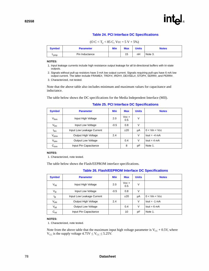
82558
NOTES:
1. Input leakage currents include high resistance output leakage for all bi-directional buffers with tri-state outputs.
2. Signals without pull-up resistors have 3 mA low output current. Signals requiring pull-ups have 6 mA low output current. The latter include FRAME#, TRDY#, IRDY#, DEVSEL#, STOP#, SERR#, and PERR#.
3. Characterized, not tested.
Note that the above table also includes minimum and maximum values for capacitance and inductance.
The table below shows the DC specifications for the Media Independent Interface (MII).
NOTES:
1. Characterized, note tested.
The table below shows the Flash/EEPROM interface specifications.
NOTES:
1. Characterized, note tested.
Note from the above table that the maximum input high voltage parameter is VCC + 0.5V, where VCC is the supply voltage 4.75V < VCC < 5.25V.
Lpinp Pin Inductance 15 nH Note 3.
Table 24. PCI Interface DC Specifications
(O C < Tc < 85 C, Vcc = 5 V + 5%)
Symbol Parameter Min Max Units Notes
Table 25. PCI Interface DC Specifications
Symbol Parameter Min Max Units Notes
Vihm Input High Voltage 2.0 Vcc + 0.5 V
Vilm Input Low Voltage -0.5 0.8 V
Iilm Input Low Leakage Current ±20 µA 0 < Vin < Vcc
Vohm Output High Voltage 2.4 V Iout = -4 mA
Volm Output Low Voltage 0.4 V Iout = 4 mA
Cinm Input Pin Capacitance 8 pF Note 1.
Table 26. Flash/EEPROM Interface DC Specifications
Symbol Parameter Min Max Units Notes
Vihl Input High Voltage 2.0 Vcc + 0.5 V
Vill Input Low Voltage -0.5 0.8 V
Iill Input Low Leakage Current ±20 µA 0 < Vin < Vcc
Vohl Output High Voltage 2.4 V Iout = -1 mA
Voll Output Low Voltage 0.4 V Iout = 6 mA
Cinl Input Pin Capacitance 10 pF Note 1.
78 Datasheet

82558
s that
The table below shows the minimum and maximum voltage and current characteristics for 100BASE-TX.
NOTES:
1. Transmitter current is measured with a 1:1 transformer on center tap.
Note the current is measured on all Vcc pins, where Vcc = 5.25V.
The table below shows the minimum and maximum voltage and current characteristics for 10BASE-T.
NOTES:
1. Transmitter current is measured with a 1:1 transformer on center tap.
Note the current is measured on all Vcc pins, where Vcc = 5.25V. The above table also showthe typical value for the transmitter current is 110 mA.
Table 27. 100BASE-TX Voltage/Current Characteristics
Symbol Parameter Min Max Units Notes
Rid100 Input Differential Resistance 10 KΩ DC
Vida100Input Differential Accept Peak
Voltage ±500 mV
Vidr100Input Differential Reject Peak
Voltage ±100 mV
Vicm100 Input Common Mode Voltage V Typical = Vcc/2
Vod100 Output Differential Peak Voltage 0.95 1.05 V Typical = 1.00 V
Icct100 Line Driver Supply mATypical = 40 mA
Note 1.
Table 28. 10BASE-T Voltage/Current Characteristics
Symbol Parameter Min Max Units Notes
Rid10 Input Differential Resistance 10 KΩ DC
Vida10Input Differential Accept Peak
Voltage ±585 +3100 mV 5 MHz ≤ f ≤ 10 MHz
Vidr10Input Differential Reject Peak
Voltage ±150 mV 0 < Vin < Vcc
Vicm10 Input Common Mode Voltage V Typical = Vcc/2
Vod10 Output Differential Peak Voltage 2.2 2.8 V Iout = 6 mA
Icct10 Line Driver Supply mATypical = 110 mA
Note 1.
Datasheet 79

82558
6.3 AC Specifications
6.3.1 PCI Interface
Table 29 below shows the specifications for PCI signaling.
NOTES:
1. Specifications are not relevant to PME#, SERR#, or INTA#, which are open drain outputs.
2. Minimum current requirements for Ioh(AC) and Icl are defined by equations A and BEquation A: Ioh = -44 + (Vout - 1.4)/0.024 for Vcc > Vout > 3.1VEquation B: Icl = -25 + (Vin + 1)/0.015 for 0V < Vout < 0.71V
3. Maximum current requirements will be met as drivers pull beyond the first step voltage (AC drive point). Equations C and D below define these maximums. In order to facilitate component testing, a maximum current test point is defined for each side of the output driver.
Equation A: Ioh = 11.9 * (Vout - 5.25) * (Vout + 2.45) for Vcc > Vout > 3.1VEquation B: Iol = 78.5 * Vout * (4.4 - Vout) for 0V < Vout < 0.71V
Table 29. PCI Signaling AC Specifications
(0 C < Tc < 85 C, Vcc = 5V + 5%)
Symbol Parameter Condition Min Max Units Notes
Ioh(AC) Switching 0 < Vout ≤ 1.4 -44 mA Note 1
Current High 1.4 < Vout < 2.4 Eqn A Eqn C mA Notes 1, 2, and 3
(Test Point) Vout = 3.1 -142 mA Note 3
Iol(AC) Switching Vout ≥ 2.2 95 mA Note 1
Current Low 2.2 Vout > 0.55 Vout/0.023 Eqn D mA Notes 1 and 3
(Test Point) Vout = 0.71 206 mA Note 3
IclLow Clamp
Current -5 < Vin ≤ -1 Eqn B mA Note 2
trUnloaded Output
Rise Time 0.4V to 2.4V 1 5 V/ns
tfUnloaded Output
Fall Time 2.4V to 0.4V 1 5 V/ns
80 Datasheet
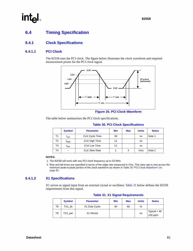
82558
6.4 Timing Specification
6.4.1 Clock Specifications
6.4.1.1 PCI Clock
The 82558 uses the PCI clock. The figure below illustrates the clock waveform and requiredmeasurement points for the PCI clock signal.
The table below summarizes the PCI clock specifications.
NOTES:
1. The 82558 will work with any PCI clock frequency up to 33 MHz.
2. Rise and fall times are specified in terms of the edge rate measured in V/ns. This slew rate is met across the minimum peak-to-peak portion of the clock waveform as shown in Table 25 “PCI Clock Waveform” on page 81.
6.4.1.2 X1 Specifications
X1 serves as signal input from an external crystal or oscillator. Table 31 below defines the 82558 requirements from this signal.
Figure 25. PCI Clock Waveform
2.4V
2.0V
1.5V
0.8V
0.4V
2V p-to-p(minimum)
T_high T_low
T_cyc
Table 30. PCI Clock Specifications
Symbol Parameter Min Max Units Notes
T1 tcyc CLK Cycle Time 30 ns Note 1
T2 thigh CLK High Time 11 ns
T3 tlow CLK Low Time 11 ns
T4 -- CLK Slew Rate 1 4 V/ns Note 2
Table 31. X1 Signal Requirements
Symbol Parameter Min Max Units Notes
T8 TX1_dc X1 Duty Cycle 40 60 %
T9 TX1_per X1 Period nsTypical = 40
±50 ppm
Datasheet 81

82558
h olled
6.4.2 Timing Parameters
6.4.2.1 PCI Timings
The table below provides the timing parameters for PCI signaling environments.
NOTES:
1. Minimum times are specified with 0 pF equivalent load; and maximum times, with 50 pF equivalent load. Actual test capacitance may vary, but results are correlated to these specifications.
2. REQ# and GNT# are point-to-point signals and have different output valid delay and input setup times than do bussed signals. All other signals are bussed.
3. RST# is asserted and de-asserted asynchronously with respect to CLK.
4. All PCI interface output drivers are floated when RST# is active.
6.4.2.2 Flash Timings
The 82558 is designed to support Flash of up to 150 ns access time. The Vpp signal in Flasimplementation should be connected permanently to 12 V. Thus, writing to the Flash is contronly by the FLWE# signal.
The table below provides the timing parameters for Flash interface signals.
Table 32. PCI Timing Parameters
Symbol Parameter Min Max Units Notes
T14 TvalCLK to Signal Valid Delay
(bussed signals) 2 11 ns Notes 1 and 2
T15 tval(ptp) CLK to Signal Valid Delay (point to point) 2 12 ns Notes 1 and
2
T16 Ton Float to Active Delay 2 ns
T17 Toff Active Float Delay 1 28 ns
T18 TsuInput Setup Time to CLK
(bussed signals) 7 ns Note 2
T19 Tsu(ptp) Input Setup Time to CLK (point to point) 10 ns Note 2
T20 Th Input Hold Time from CLK 0 ns
T21 trstReset Active Time After
Power Stable 1 ms Note 3
T22 trst-clkReset Active Time After CLK
Stable 100 µs Note 3
T23 trst-offReset Active to Output Float
Delay 40 ns Notes 3 and 4
Table 33. Flash Interface Timing Parameters
Symbol Parameter Min Max Units Notes
T35 tflrwc Read/Write Cycle Time 150 nsNote 1; Flash tAVAV = 150 ns
T36 tflaccFLADDR to Read FLD Setup
Time 150 nsNote 1; Flash tAVQV = 150 ns
82 Datasheet
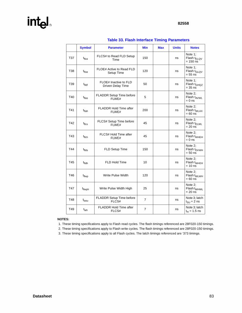
82558
NOTES:
1. These timing specifications apply to Flash read cycles. The flash timings referenced are 28F020-150 timings.
2. These timing specifications apply to Flash write cycles. The flash timings referenced are 28F020-150 timings.
3. These timing specifications apply to all Flash cycles. The latch timings referenced are ‘373 timings.
T37 tflceFLCS# to Read FLD Setup
Time 150 nsNote 1; Flash tELQV = 150 ns
T38 tfloeFLOE# Active to Read FLD
Setup Time 120 nsNote 1; Flash tGLQV = 55 ns
T39 tfldfFLOE# Inactive to FLD
Driven Delay Time 50 nsNote 1; Flash tGHQZ = 35 ns
T40 tflasFLADDR Setup Time before
FLWE# 5 nsNote 2; Flash tAVWL = 0 ns
T41 tflahFLADDR Hold Time after
FLWE# 200 nsNote 2; Flash tWLAX = 60 ns
T42 tflcsFLCS# Setup Time before
FLWE# 45 nsNote 2; Flash tELWL = 20 ns
T43 tflchFLCS# Hold Time after
FLWE# 45 nsNote 2; Flash tWHEH = 0 ns
T44 tflds FLD Setup Time 150 nsNote 2; Flash tDVWH = 50 ns
T45 tfldh FLD Hold Time 10 nsNote 2; Flash tWHDX = 10 ns
T46 tflwp Write Pulse Width 120 nsNote 2; Flash tWLWH = 60 ns
T47 tflwph Write Pulse Width High 25 nsNote 2; Flash tWHWL = 20 ns
T48 tlasuFLADDR Setup Time before
FLCS# 7 ns Note 3; latch tSU = 2 ns
T49 tlahFLADDR Hold Time after
FLCS# 7 ns Note 3; latch tH = 1.5 ns
Table 33. Flash Interface Timing Parameters
Symbol Parameter Min Max Units Notes
Datasheet 83

82558
signal.
The timing parameters are for Flash write and read cycles are illustrated in Figure 26 and Figure 27 below.
Note: The Flash write cycle operates with the FLWE# signal; and the Flash read cycle, the FLOE#
6.4.2.3 EEPROM Timings
The 82558 is designed to support a standard 64x16 serial EEPROM. Table 34 provides the timing parameters for EEPROM interface signals.
Figure 26. Flash Timing - Write Cycle
Figure 27. Flash Timing - Read Cycle
Address StableFLADDR
T41T40
T35
FLCS#
FLWE#
FLDATA-W Data Out
T44 T45
T43T42 T46
T47
T49T48
Address StableFLADDR
FLCS#
FLOE#
T38
FLDATA-R Data In
T37
T35
T36 T39
Table 34. EEPROM Interface Timing Parameters
Symbol Parameter Min Max Units Notes
T50 tEFSK Serial Clock Frequency 1.0 MHz EEPROM fsk = 1 MHz
T51 tECSSDelay from CS High to SK
High 300 ns EEPROM tcss = 50 ns
T52 tECSHDelay from SK Low to CS
Low 30 ns EEPROM tcsh = 0 ns
84 Datasheet

82558
The timing parameters for the EEPROM interface are illustrated in the figure below.
6.4.2.4 PHY Timings
The table below summarizes the 10BASE-T link pulse timing parameters.
10BASE-T link pulse timing is illustrated in the figure below.
T53 tEDIS Setup Time of DI to SK 300 nsEEPROM tdis = 150 ns
T54 tEDIHFLOE# Inactive to FLD
Driven Delay Time 50 nsEEPROM tdih = 150 ns
T55 tECSFLADDR Setup Time before
FLWE# 5 nsEEPROM tcs = 250 ns
Table 34. EEPROM Interface Timing Parameters
Symbol Parameter Min Max Units Notes
Figure 28. EEPROM Timing
T51
EECS
FLD0EESK
FLD2EEDI
T53 T54
T52
Table 35. 10BASE-T Normal Link Pulse Timing Parameters
Symbol Parameter Min Max Units Notes
T56 Tnlp_wid NLP Width ns Typical = 100 ns
T57 Tnlp_per NLP Period 8 24 ms
Figure 29. 10BASE-T Normal Link Pulse Timing
Normal Link Pulse
T57
T56
Datasheet 85

82558
The table below summarizes the Auto-Negotiation fast link pulse timing parameters.
Auto-Negotiation link pulse timing is illustrated in the figure below.
The table below summarizes the 100BASE-TX timing specifications for AC timing.
Table 36. Auto-Negotiation Fast Link Pulse Timing Parameters
Symbol Parameter Min Max Units Notes
T58 Tflp_wid FLP Width (clock/data) ns Typical = 100 ns
T59 Tflp_clk_clkClock Pulse to Clock Pulse
Period 111 139 µs Typical = 125 µs
T60 Tflp_clk_datClock Pulse to Data Pulse
Period 55.5 69.5 µs Typical = 62.5 µs
T61 Tflp_bur_numNumber of Pulses in One
Burst 17 33
T62 Tflp_bur_wid Burst Width msTypical =
2 ms
T63 Tflp_bur_per FLP Burst Period 8 24 ms
Figure 30. Auto-Negotiation Fast Link Pulse Timing
Fast Link Pulse
T59
T60
T58
Clock Pulse Data Pulse Clock Pulse
FLP Bursts
T62T63
Table 37. 100BASE-TX Transmitter AC Timing Specification
Symbol Parameter Min Max Units Notes
T64 TjitTDP/TDN Differential Output
Peak Jitter 700 psHLS Data;
Typical = 700 ps
86 Datasheet
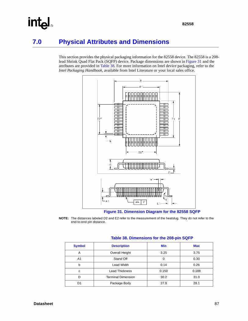
82558
a 208-
7.0 Physical Attributes and Dimensions
This section provides the physical packaging information for the 82558 device. The 82558 is lead Shrink Quad Flat Pack (SQFP) device. Package dimensions are shown in Figure 31 and the attributes are provided in Table 38. For more information on Intel device packaging, refer to theIntel Packaging Handbook, available from Intel Literature or your local sales office.
NOTE: The distances labeled D2 and E2 refer to the measurement of the heatslug. They do not refer to the end-to-end pin distance.
Figure 31. Dimension Diagram for the 82558 SQFP
Table 38. Dimensions for the 208-pin SQFP
Symbol Description Min Max
A Overall Height 3.25 3.75
A1 Stand Off 0 0.30
b Lead Width 0.14 0.26
c Lead Thickness 0.150 0.188
D Terminal Dimension 30.2 31.0
D1 Package Body 27.9 28.1
Datasheet 87

82558
NOTE: All dimensions are in millimeters except T, which is in degrees.
E Terminal Dimension 30.2 31.0
E1 Package Body 27.9 28.1
e1 Lead Pitch 0.40 0.60
L1 Foot Length 0.30 0.70
T Lead Angle 0.0° 10.0°Y Coplanarity 0.1 0.1
D2/E2 Heatslug 21 21
Table 38. Dimensions for the 208-pin SQFP
Symbol Description Min Max
88 Datasheet

Datasheet 89
82558
8.0 Revision History
Revision Date Version Description
5-97 New Preliminary Release, Revision 1.1.
9/97 2.0 82558 B-step features added
10/97 2.2 82558 B-step features updated
1/98 2.3 General editing