8051, 8052 and 80c51 hardware description
TRANSCRIPT
December 1992
8051, 8052 and 80C51Hardware Description
COPYRIGHT © INTEL CORPORATION, 1996
Order Number: 270252-006
8051, 8052 and 80C51 Hardware Description
CONTENTS PAGE
INTRODUCTION ÀÀÀÀÀÀÀÀÀÀÀÀÀÀÀÀÀÀÀÀÀÀÀÀÀÀÀ 1
Special Function Registers ÀÀÀÀÀÀÀÀÀÀÀÀÀÀÀÀÀ 1
PORT STRUCTURES ANDOPERATION ÀÀÀÀÀÀÀÀÀÀÀÀÀÀÀÀÀÀÀÀÀÀÀÀÀÀÀÀ 4
I/O Configurations ÀÀÀÀÀÀÀÀÀÀÀÀÀÀÀÀÀÀÀÀÀÀÀÀÀ 5
Writing to a Port ÀÀÀÀÀÀÀÀÀÀÀÀÀÀÀÀÀÀÀÀÀÀÀÀÀÀÀÀ 5
Port Loading and Interfacing ÀÀÀÀÀÀÀÀÀÀÀÀÀÀÀÀ 6
Read-Modify-Write Feature ÀÀÀÀÀÀÀÀÀÀÀÀÀÀÀÀÀ 7
ACCESSING EXTERNAL MEMORY ÀÀÀÀÀÀÀ 7
TIMER/COUNTERS ÀÀÀÀÀÀÀÀÀÀÀÀÀÀÀÀÀÀÀÀÀÀÀ 7
Timer 0 and Timer 1 ÀÀÀÀÀÀÀÀÀÀÀÀÀÀÀÀÀÀÀÀÀÀÀÀ 8
Timer 2 ÀÀÀÀÀÀÀÀÀÀÀÀÀÀÀÀÀÀÀÀÀÀÀÀÀÀÀÀÀÀÀÀÀÀÀ 10
SERIAL INTERFACE ÀÀÀÀÀÀÀÀÀÀÀÀÀÀÀÀÀÀÀÀÀ 11
Multiprocessor Communications ÀÀÀÀÀÀÀÀÀÀÀ 12
Serial Port Control Register ÀÀÀÀÀÀÀÀÀÀÀÀÀÀÀÀ 12
Baud Rates ÀÀÀÀÀÀÀÀÀÀÀÀÀÀÀÀÀÀÀÀÀÀÀÀÀÀÀÀÀÀÀ 13
More About Mode 0 ÀÀÀÀÀÀÀÀÀÀÀÀÀÀÀÀÀÀÀÀÀÀÀ 15
More About Mode 1 ÀÀÀÀÀÀÀÀÀÀÀÀÀÀÀÀÀÀÀÀÀÀÀ 15
More About Modes 2 and 3 ÀÀÀÀÀÀÀÀÀÀÀÀÀÀÀÀ 18
CONTENTS PAGE
INTERRUPTS ÀÀÀÀÀÀÀÀÀÀÀÀÀÀÀÀÀÀÀÀÀÀÀÀÀÀÀÀ 21
Priority Level Structure ÀÀÀÀÀÀÀÀÀÀÀÀÀÀÀÀÀÀÀÀ 22
How Interrupts Are Handled ÀÀÀÀÀÀÀÀÀÀÀÀÀÀÀ 22
External Interrupts ÀÀÀÀÀÀÀÀÀÀÀÀÀÀÀÀÀÀÀÀÀÀÀÀ 23
Response Time ÀÀÀÀÀÀÀÀÀÀÀÀÀÀÀÀÀÀÀÀÀÀÀÀÀÀÀ 23
SINGLE-STEP OPERATION ÀÀÀÀÀÀÀÀÀÀÀÀÀÀ 24
RESET ÀÀÀÀÀÀÀÀÀÀÀÀÀÀÀÀÀÀÀÀÀÀÀÀÀÀÀÀÀÀÀÀÀÀÀ 24
POWER-ON RESET ÀÀÀÀÀÀÀÀÀÀÀÀÀÀÀÀÀÀÀÀÀÀ 25
POWER-SAVING MODES OFOPERATION ÀÀÀÀÀÀÀÀÀÀÀÀÀÀÀÀÀÀÀÀÀÀÀÀÀÀÀ 25
CHMOS Power Reduction Modes ÀÀÀÀÀÀÀÀÀ 25
EPROM VERSIONS ÀÀÀÀÀÀÀÀÀÀÀÀÀÀÀÀÀÀÀÀÀÀ 27
Exposure to Light ÀÀÀÀÀÀÀÀÀÀÀÀÀÀÀÀÀÀÀÀÀÀÀÀÀ 27
Program Memory Locks ÀÀÀÀÀÀÀÀÀÀÀÀÀÀÀÀÀÀÀ 27
ONCE Mode ÀÀÀÀÀÀÀÀÀÀÀÀÀÀÀÀÀÀÀÀÀÀÀÀÀÀÀÀÀÀ 28
THE ON-CHIP OSCILLATORS ÀÀÀÀÀÀÀÀÀÀÀ 28
HMOS Versions ÀÀÀÀÀÀÀÀÀÀÀÀÀÀÀÀÀÀÀÀÀÀÀÀÀÀÀ 28
CHMOS Versions ÀÀÀÀÀÀÀÀÀÀÀÀÀÀÀÀÀÀÀÀÀÀÀÀÀ 30
INTERNAL TIMING ÀÀÀÀÀÀÀÀÀÀÀÀÀÀÀÀÀÀÀÀÀÀÀ 31
8051, 8052 AND 80C51HARDWARE DESCRIPTION
INTRODUCTION
This chapter presents a comprehensive description ofthe on-chip hardware features of the MCSÉ-51 micro-controllers. Included in this description are
# The port drivers and how they function both asports and, for Ports 0 and 2, in bus operations
# The Timer/Counters
# The Serial Interface
# The Interrupt System
# Reset
# The Reduced Power Modes in the CHMOS devices
# The EPROM versions of the 8051AH, 8052AH and80C51BH
The devices under consideration are listed in Table 1.As it becomes unwieldy to be constantly referring toeach of these devices by their individual names, we willadopt a convention of referring to them generically as8051s and 8052s, unless a specific member of the groupis being referred to, in which case it will be specificallynamed. The ‘‘8051s’’ include the 8051AH, 80C51BH,and their ROMless and EPROM versions. The ‘‘8052s’’are the 8052AH, 8032AH and 8752BH.
Figure 1 shows a functional block diagram of the 8051sand 8052s.
Table 1. The MCS-51 Family of Microcontrollers
Device ROMless EPROM ROM RAM 16-bit Ckt
Name Version Version Bytes Bytes Timers Type
8051AH 8031AH 8751H, 8751BH 4K 128 2 HMOS
8052AH 8032AH 8752BH 8K 256 3 HMOS
80C51BH 80C31BH 87C51 4K 128 2 CHMOS
Special Function Registers
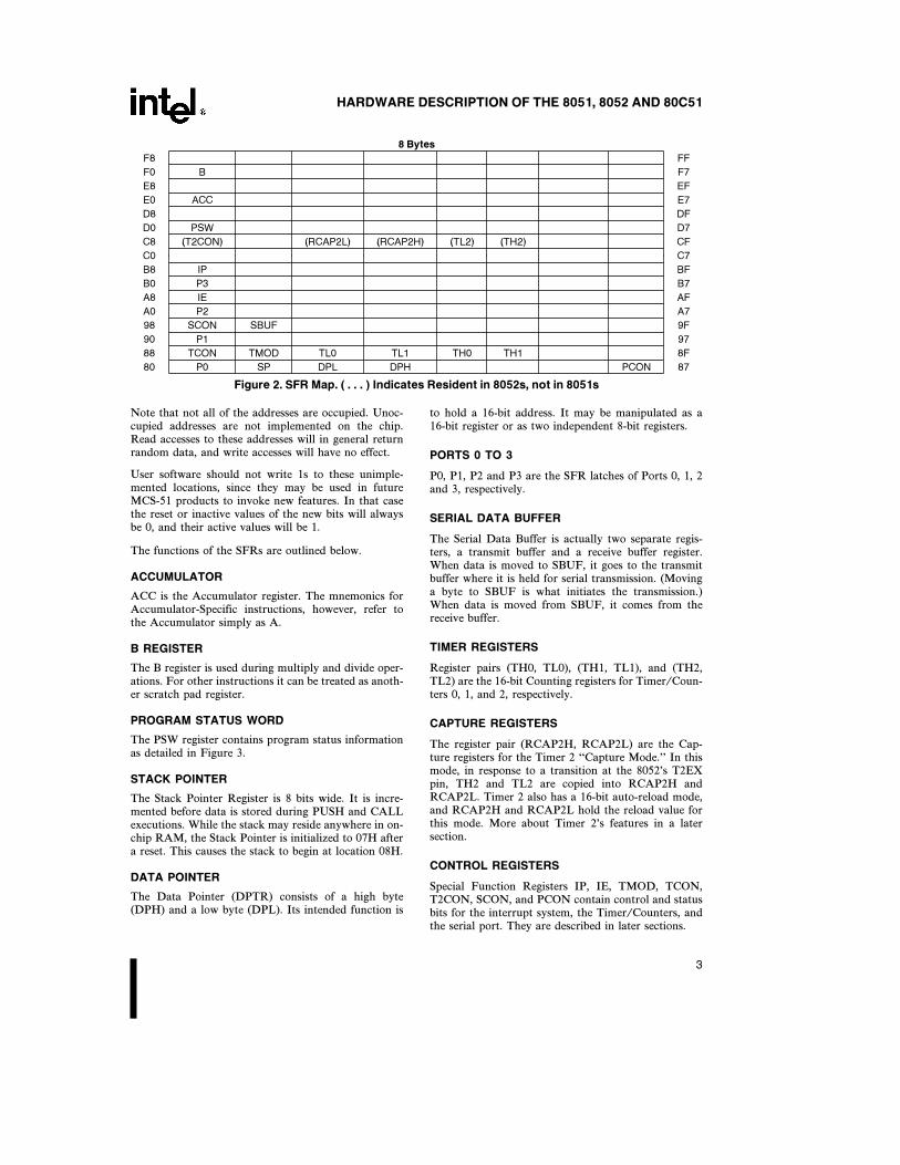
A map of the on-chip memory area called SFR (Special Function Register) space is shown in Figure 2. SFRs markedby parentheses are resident in the 8052s but not in the 8051s.
1
HARDWARE DESCRIPTION OF THE 8051, 8052 AND 80C51
270252–1
Figure 1. MCS-51 Architectural Block Diagram
2
HARDWARE DESCRIPTION OF THE 8051, 8052 AND 80C51
8 Bytes
F8 FF
F0 B F7
E8 EF
E0 ACC E7
D8 DF
D0 PSW D7
C8 (T2CON) (RCAP2L) (RCAP2H) (TL2) (TH2) CF
C0 C7
B8 IP BF
B0 P3 B7
A8 IE AF
A0 P2 A7
98 SCON SBUF 9F
90 P1 97
88 TCON TMOD TL0 TL1 TH0 TH1 8F
80 P0 SP DPL DPH PCON 87
Figure 2. SFR Map. ( . . . ) Indicates Resident in 8052s, not in 8051s
Note that not all of the addresses are occupied. Unoc-cupied addresses are not implemented on the chip.Read accesses to these addresses will in general returnrandom data, and write accesses will have no effect.
User software should not write 1s to these unimple-mented locations, since they may be used in futureMCS-51 products to invoke new features. In that casethe reset or inactive values of the new bits will alwaysbe 0, and their active values will be 1.
The functions of the SFRs are outlined below.
ACCUMULATOR
ACC is the Accumulator register. The mnemonics forAccumulator-Specific instructions, however, refer tothe Accumulator simply as A.
B REGISTER
The B register is used during multiply and divide oper-ations. For other instructions it can be treated as anoth-er scratch pad register.
PROGRAM STATUS WORD
The PSW register contains program status informationas detailed in Figure 3.
STACK POINTER
The Stack Pointer Register is 8 bits wide. It is incre-mented before data is stored during PUSH and CALLexecutions. While the stack may reside anywhere in on-chip RAM, the Stack Pointer is initialized to 07H aftera reset. This causes the stack to begin at location 08H.
DATA POINTER
The Data Pointer (DPTR) consists of a high byte(DPH) and a low byte (DPL). Its intended function is
to hold a 16-bit address. It may be manipulated as a16-bit register or as two independent 8-bit registers.
PORTS 0 TO 3
P0, P1, P2 and P3 are the SFR latches of Ports 0, 1, 2and 3, respectively.
SERIAL DATA BUFFER
The Serial Data Buffer is actually two separate regis-ters, a transmit buffer and a receive buffer register.When data is moved to SBUF, it goes to the transmitbuffer where it is held for serial transmission. (Movinga byte to SBUF is what initiates the transmission.)When data is moved from SBUF, it comes from thereceive buffer.
TIMER REGISTERS
Register pairs (TH0, TL0), (TH1, TL1), and (TH2,TL2) are the 16-bit Counting registers for Timer/Coun-ters 0, 1, and 2, respectively.
CAPTURE REGISTERS
The register pair (RCAP2H, RCAP2L) are the Cap-ture registers for the Timer 2 ‘‘Capture Mode.’’ In thismode, in response to a transition at the 8052’s T2EXpin, TH2 and TL2 are copied into RCAP2H andRCAP2L. Timer 2 also has a 16-bit auto-reload mode,and RCAP2H and RCAP2L hold the reload value forthis mode. More about Timer 2’s features in a latersection.
CONTROL REGISTERS
Special Function Registers IP, IE, TMOD, TCON,T2CON, SCON, and PCON contain control and statusbits for the interrupt system, the Timer/Counters, andthe serial port. They are described in later sections.
3

HARDWARE DESCRIPTION OF THE 8051, 8052 AND 80C51
(MSB) (LSB)
CY AC F0 RS1 RS0 OV Ð P
Symbol Position Name and Significance
CY PSW.7 Carry flag.
AC PSW.6 Auxiliary Carry flag.
(For BCD operations.)
F0 PSW.5 Flag 0
(Available to the user for general
purposes.)
RS1 PSW.4 Register bank select control bits 1 &
RS0 PSW.3 0. Set/cleared by software to
determine working register bank (see
Note).
Symbol Position Name and Significance
OV PSW.2 Overflow flag.
Ð PSW.1 User definable flag.
P PSW.0 Parity flag.
Set/cleared by hardware each
instruction cycle to indicate an odd/
even number of ‘‘one’’ bits in the
Accumulator, i.e., even parity.NOTE:The contents of (RS1, RS0) enable the working register banks asfollows:
(0.0)ÐBank 0 (00H–07H)(0.1)ÐBank 1 (08H–0FH)(1.0)ÐBank 2 (10H–17H)(1.1)ÐBank 3 (18H–1FH)
Figure 3. PSW: Program Status Word Register
270252–2
A. Port 0 Bit
270252–4
C. Port 2 Bit
270252–3
B. Port 1 Bit
270252–5
D. Port 3 Bit
Figure 4. 8051 Port Bit Latches and I/O Buffers*See Figure 5 for details of the internal pullup.
PORT STRUCTURES ANDOPERATION
All four ports in the 8051 are bidirectional. Each con-sists of a latch (Special Function Registers P0 throughP3), an output driver, and an input buffer.
The output drivers of Ports 0 and 2, and the input buff-ers of Port 0, are used in accesses to external memory.In this application, Port 0 outputs the low byte of the
external memory address, time-multiplexed with thebyte being written or read. Port 2 outputs the high byteof the external memory address when the address is 16bits wide. Otherwise the Port 2 pins continue to emitthe P2 SFR content.
All the Port 3 pins, and (in the 8052) two Port 1 pinsare multifunctional. They are not only port pins, butalso serve the functions of various special features aslisted on the following page.
4

HARDWARE DESCRIPTION OF THE 8051, 8052 AND 80C51
Port Pin Alternate Function
*P1.0 T2 (Timer/Counter 2
external input)
*P1.1 T2EX (Timer/Counter 2
Capture/Reload trigger)
P3.0 RXD (serial input port)
P3.1 TXD (serial output port)
P3.2 INT0 (external interrupt)
P3.3 INT1 (external interrupt)
P3.4 T0 (Timer/Counter 0 external
input)
P3.5 T1 (Timer/Counter 1 external
input)
P3.6 WR (external Data Memory
write strobe)
P3.7 RD (external Data Memory
read strobe)
*P1.0 and P1.1 serve these alternate functions only onthe 8052.
The alternate functions can only be activated if the cor-responding bit latch in the port SFR contains a 1. Oth-erwise the port pin is stuck at 0.
I/O Configurations
Figure 4 shows a functional diagram of a typical bitlatch and I/O buffer in each of the four ports. The bitlatch (one bit in the port’s SFR) is represented as aType D flip-flop, which will clock in a value from theinternal bus in response to a ‘‘write to latch’’ signalfrom the CPU. The Q output of the flip-flop is placedon the internal bus in response to a ‘‘read latch’’ signalfrom the CPU. The level of the port pin itself is placedon the internal bus in response to a ‘‘read pin’’ signalfrom the CPU. Some instructions that read a port acti-vate the ‘‘read latch’’ signal, and others activate the‘‘read pin’’ signal. More about that later.
As shown in Figure 4, the output drivers of Ports 0 and2 are switchable to an internal ADDR and ADDR/DATA bus by an internal CONTROL signal for use inexternal memory accesses. During external memory ac-cesses, the P2 SFR remains unchanged, but the P0 SFRgets 1s written to it.
Also shown in Figure 4, is that if a P3 bit latch containsa 1, then the output level is controlled by the signallabeled ‘‘alternate output function.’’ The actual P3.Xpin level is always available to the pin’s alternate inputfunction, if any.
Ports 1, 2, and 3 have internal pullups. Port 0 has opendrain outputs. Each I/O line can be independently usedas an input or an output. (Ports 0 and 2 may not beused as general purpose I/O when being used as the
ADDR/DATA BUS). To be used as an input, the portbit latch must contain a 1, which turns off the outputdriver FET. Then, for Ports 1, 2, and 3, the pin ispulled high by the internal pullup, but can be pulledlow by an external source.
Port 0 differs in not having internal pullups. The pullupFET in the P0 output driver (see Figure 4) is used onlywhen the Port is emitting 1s during external memoryaccesses. Otherwise the pullup FET is off. Consequent-ly P0 lines that are being used as output port lines areopen drain. Writing a 1 to the bit latch leaves bothoutput FETs off, so the pin floats. In that condition itcan be used a high-impedance input.
Because Ports 1, 2, and 3 have fixed internal pullupsthey are sometimes called ‘‘quasi-bidirectional’’ ports.When configured as inputs they pull high and willsource current (IIL, in the data sheets) when externallypulled low. Port 0, on the other hand, is considered‘‘true’’ bidirectional, because when configured as an in-put it floats.
All the port latches in the 8051 have 1s written to themby the reset function. If a 0 is subsequently written to aport latch, it can be reconfigured as an input by writinga 1 to it.
Writing to a Port
In the execution of an instruction that changes the val-ue in a port latch, the new value arrives at the latchduring S6P2 of the final cycle of the instruction. How-ever, port latches are in fact sampled by their outputbuffers only during Phase 1 of any clock period. (Dur-ing Phase 2 the output buffer holds the value it sawduring the previous Phase 1). Consequently, the newvalue in the port latch won’t actually appear at theoutput pin until the next Phase 1, which will be at S1P1of the next machine cycle. See Figure 39 in the InternalTiming section.
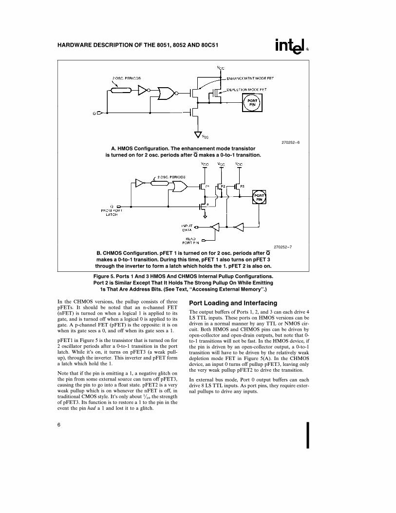
If the change requires a 0-to-1 transition in Port 1, 2, or3, an additional pullup is turned on during S1P1 andS1P2 of the cycle in which the transition occurs. This isdone to increase the transition speed. The extra pullupcan source about 100 times the current that the normalpullup can. It should be noted that the internal pullupsare field-effect transistors, not linear resistors. The pull-up arrangements are shown in Figure 5.
In HMOS versions of the 8051, the fixed part of thepullup is a depletion-mode transistor with the gatewired to the source. This transistor will allow the pin tosource about 0.25 mA when shorted to ground. Inparallel with the fixed pullup is an enhancement-modetransistor, which is activated during S1 whenever theport bit does a 0-to-1 transition. During this interval, ifthe port pin is shorted to ground, this extra transistorwill allow the pin to source an additional 30 mA.
5
HARDWARE DESCRIPTION OF THE 8051, 8052 AND 80C51
270252–6
A. HMOS Configuration. The enhancement mode transistor
is turned on for 2 osc. periods after Q makes a 0-to-1 transition.
270252–7
B. CHMOS Configuration. pFET 1 is turned on for 2 osc. periods after Q
makes a 0-to-1 transition. During this time, pFET 1 also turns on pFET 3
through the inverter to form a latch which holds the 1. pFET 2 is also on.
Figure 5. Ports 1 And 3 HMOS And CHMOS Internal Pullup Configurations.
Port 2 is Similar Except That It Holds The Strong Pullup On While Emitting
1s That Are Address Bits. (See Text, ‘‘Accessing External Memory’’.)
In the CHMOS versions, the pullup consists of threepFETs. It should be noted that an n-channel FET(nFET) is turned on when a logical 1 is applied to itsgate, and is turned off when a logical 0 is applied to itsgate. A p-channel FET (pFET) is the opposite: it is onwhen its gate sees a 0, and off when its gate sees a 1.
pFET1 in Figure 5 is the transistor that is turned on for2 oscillator periods after a 0-to-1 transition in the portlatch. While it’s on, it turns on pFET3 (a weak pull-up), through the inverter. This inverter and pFET forma latch which hold the 1.
Note that if the pin is emitting a 1, a negative glitch onthe pin from some external source can turn off pFET3,causing the pin to go into a float state. pFET2 is a veryweak pullup which is on whenever the nFET is off, intraditional CMOS style. It’s only about (/10 the strengthof pFET3. Its function is to restore a 1 to the pin in theevent the pin had a 1 and lost it to a glitch.
Port Loading and Interfacing
The output buffers of Ports 1, 2, and 3 can each drive 4LS TTL inputs. These ports on HMOS versions can bedriven in a normal manner by any TTL or NMOS cir-cuit. Both HMOS and CHMOS pins can be driven byopen-collector and open-drain outputs, but note that 0-to-1 transitions will not be fast. In the HMOS device, ifthe pin is driven by an open-collector output, a 0-to-1transition will have to be driven by the relatively weakdepletion mode FET in Figure 5(A). In the CHMOSdevice, an input 0 turns off pullup pFET3, leaving onlythe very weak pullup pFET2 to drive the transition.
In external bus mode, Port 0 output buffers can eachdrive 8 LS TTL inputs. As port pins, they require exter-nal pullups to drive any inputs.
6
HARDWARE DESCRIPTION OF THE 8051, 8052 AND 80C51
Read-Modify-Write Feature
Some instructions that read a port read the latch andothers read the pin. Which ones do which? The instruc-tions that read the latch rather than the pin are the onesthat read a value, possibly change it, and then rewrite itto the latch. These are called ‘‘read-modify-write’’ in-structions. The instructions listed below are read-mod-ify-write instructions. When the destination operand isa port, or a port bit, these instructions read the latchrather than the pin:
ANL (logical AND, e.g., ANL P1, A)
ORL (logical OR, e.g., ORL P2, A)
XRL (logical EX-OR, e.g., XRL P3, A)
JBC (jump if bit e 1 and clear bit, e.g.,JBC P1.1, LABEL)
CPL (complement bit, e.g., CPL P3.0)
INC (increment, e.g., INC P2)
DEC (decrement, e.g., DEC P2)
DJNZ (decrement and jump if not zero, e.g.,DJNZ P3, LABEL)
MOV, PX.Y, C (move carry bit to bit Y of Port X)
CLR PX.Y (clear bit Y of Port X)
SETB PX.Y (set bit Y of Port X)
It is not obvious that the last three instructions in thislist are read-modify-write instructions, but they are.They read the port byte, all 8 bits, modify the addressedbit, then write the new byte back to the latch.
The reason that read-modify-write instructions are di-rected to the latch rather than the pin is to avoid apossible misinterpretation of the voltage level at thepin. For example, a port bit might be used to drive thebase of a transistor. When a 1 is written to the bit, thetransistor is turned on. If the CPU then reads the sameport bit at the pin rather than the latch, it will read thebase voltage of the transistor and interpret it as a 0.Reading the latch rather than the pin will return thecorrect value of 1.
ACCESSING EXTERNAL MEMORY
Accesses to external memory are of two types: accessesto external Program Memory and accesses to externalData Memory. Accesses to external Program Memoryuse signal PSEN (program store enable) as the readstrobe. Accesses to external Data Memory use RD orWR (alternate functions of P3.7 and P3.6) to strobe thememory. Refer to Figures 36 through 38 in the InternalTiming section.
Fetches from external Program Memory always use a16-bit address. Accesses to external Data Memory canuse either a 16-bit address (MOVX @DPTR) or an8-bit address (MOVX @Ri).
Whenever a 16-bit address is used, the high byte of theaddress comes out on Port 2, where it is held for theduration of the read or write cycle. Note that the Port 2drivers use the strong pullups during the entire timethat they are emitting address bits that are 1s. This isduring the execution of a MOVX @DPTR instruction.During this time the Port 2 latch (the Special FunctionRegister) does not have to contain 1s, and the contentsof the Port 2 SFR are not modified. If the externalmemory cycle is not immediately followed by anotherexternal memory cycle, the undisturbed contents of thePort 2 SFR will reappear in the next cycle.
If an 8-bit address is being used (MOVX @Ri), thecontents of the Port 2 SFR remain at the Port 2 pinsthroughout the external memory cycle. This will facili-tate paging.
In any case, the low byte of the address is time-multi-plexed with the data byte on Port 0. The ADDR/DATA signal drives both FETs in the Port 0 outputbuffers. Thus, in this application the Port 0 pins are notopen-drain outputs, and do not require external pull-ups. Signal ALE (Address Latch Enable) should beused to capture the address byte into an external latch.The address byte is valid at the negative transition ofALE. Then, in a write cycle, the data byte to be writtenappears on Port 0 just before WR is activated, and re-mains there until after WR is deactivated. In a readcycle, the incoming byte is accepted at Port 0 just be-fore the read strobe is deactivated.
During any access to external memory, the CPU writes0FFH to the Port 0 latch (the Special Function Regis-ter), thus obliterating whatever information the Port 0SFR may have been holding. If the user writes to Port 0during an external memory fetch, the incoming codebyte is corrupted. Therefore, do not write to Port 0 ifexternal program memory is used.
External Program Memory is accessed under two con-ditions:
1) Whenever signal EA is active; or
2) Whenever the program counter (PC) contains anumber that is larger than 0FFFH (1FFFH for the8052).
This requires that the ROMless versions have EA wiredlow to enable the lower 4K (8K for the 8032) programbytes to be fetched from external memory.
When the CPU is executing out of external ProgramMemory, all 8 bits of Port 2 are dedicated to an outputfunction and may not be used for general purpose I/O.During external program fetches they output the highbyte of the PC. During this time the Port 2 drivers usethe strong pullups to emit PC bits that are 1s.
TIMER/COUNTERS
The 8051 has two 16-bit Timer/Counter registers: Tim-er 0 and Timer 1. The 8052 has these two plus one
7
HARDWARE DESCRIPTION OF THE 8051, 8052 AND 80C51
more: Timer 2. All three can be configured to operateeither as timers or event counters.
In the ‘‘Timer’’ function, the register is incrementedevery machine cycle. Thus, one can think of it as count-ing machine cycles. Since a machine cycle consists of 12oscillator periods, the count rate is (/12 of the oscillatorfrequency.
In the ‘‘Counter’’ function, the register is incrementedin response to a 1-to-0 transition at its correspondingexternal input pin, T0, T1 or (in the 8052) T2. In thisfunction, the external input is sampled during S5P2 ofevery machine cycle. When the samples show a high inone cycle and a low in the next cycle, the count is incre-mented. The new count value appears in the registerduring S3P1 of the cycle following the one in which thetransition was detected. Since it takes 2 machine cycles(24 oscillator periods) to recognize a 1-to-0 transition,the maximum count rate is (/24 of the oscillator fre-quency. There are no restrictions on the duty cycle ofthe external input signal, but to ensure that a givenlevel is sampled at least once before it changes, itshould be held for at least one full machine cycle.
In addition to the ‘‘Timer’’ or ‘‘Counter’’ selection,Timer 0 and Timer 1 have four operating modes fromwhich to select. Timer 2, in the 8052, has three modesof operation: ‘‘Capture,’’ ‘‘Auto-Reload’’ and ‘‘baudrate generator.’’
Timer 0 and Timer 1
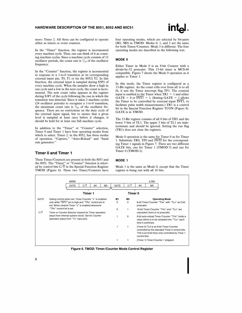
These Timer/Counters are present in both the 8051 andthe 8052. The ‘‘Timer’’ or ‘‘Counter’’ function is select-ed by control bits C/T in the Special Function RegisterTMOD (Figure 6). These two Timer/Counters have
four operating modes, which are selected by bit-pairs(M1, M0) in TMOD. Modes 0, 1, and 2 are the samefor both Timer/Counters. Mode 3 is different. The fouroperating modes are described in the following text.
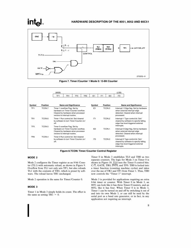
MODE 0
Either Timer in Mode 0 is an 8-bit Counter with adivide-by-32 prescaler. This 13-bit timer is MCS-48compatible. Figure 7 shows the Mode 0 operation as itapplies to Timer 1.
In this mode, the Timer register is configured as a13-Bit register. As the count rolls over from all 1s to all0s, it sets the Timer interrupt flag TF1. The countedinput is enabled to the Timer when TR1 e 1 and eitherGATE e 0 or INT1 e 1. (Setting GATE e 1 allowsthe Timer to be controlled by external input INT1, tofacilitate pulse width measurements.) TR1 is a controlbit in the Special Function Register TCON (Figure 8).GATE is in TMOD.
The 13-Bit register consists of all 8 bits of TH1 and thelower 5 bits of TL1. The upper 3 bits of TL1 are inde-terminate and should be ignored. Setting the run flag(TR1) does not clear the registers.
Mode 0 operation is the same for Timer 0 as for Timer1. Substitute TR0, TF0 and INT0 for the correspond-ing Timer 1 signals in Figure 7. There are two differentGATE bits, one for Timer 1 (TMOD.7) and one forTimer 0 (TMOD.3).
MODE 1
Mode 1 is the same as Mode 0, except that the Timerregister is being run with all 16 bits.
(MSB) (LSB)
GATE C/T M1 M0 GATE C/T M1 M0X ä YX ä YTimer 1 Timer 0
GATE Gating control when set. Timer/Counter ‘‘x’’ is enabled
only while ‘‘INTx’’ pin is high and ‘‘TRx’’ control pin is
set. When cleared Timer ‘‘x’’ is enabled whenever
‘‘TRx’’ control bit is set.
C/T Timer or Counter Selector cleared for Timer operation
(input from internal system clock). Set for Counter
operation (input from ‘‘Tx’’ input pin).
M1 M0 Operating Mode
0 0 8-bit Timer/Counter ‘‘THx’’ with ‘‘TLx’’ as 5-bit
prescaler.
0 1 16-bit Timer/Counter ‘‘THx’’ and ‘‘TLx’’ are
cascaded; there is no prescaler.
1 0 8-bit auto-reload Timer/Counter ‘‘THx’’ holds a
value which is to be reloaded into ‘‘TLx’’ each
time it overflows.
1 1 (Timer 0) TL0 is an 8-bit Timer/Counter
controlled by the standard Timer 0 control bits.
TH0 is an 8-bit timer only controlled by Timer 1
control bits.
1 1 (Timer 1) Timer/Counter 1 stopped.
Figure 6. TMOD: Timer/Counter Mode Control Register
8
HARDWARE DESCRIPTION OF THE 8051, 8052 AND 80C51
270252–9
Figure 7. Timer/Counter 1 Mode 0: 13-Bit Counter
(MSB) (LSB)
TF1 TR1 TF0 TR0 IE1 IT1 IE0 IT0
Symbol Position Name and Significance
TF1 TCON.7 Timer 1 overflow Flag. Set by
hardware on Timer/Counter overflow.
Cleared by hardware when processor
vectors to interrupt routine.
TR1 TCON.6 Timer 1 Run control bit. Set/cleared
by software to turn Timer/Counter on/
off.
TF0 TCON.5 Timer 0 overflow Flag. Set by
hardware on Timer/Counter overflow.
Cleared by hardware when processor
vectors to interrupt routine.
TR0 TCON.4 Timer 0 Run control bit. Set/cleared
by software to turn Timer/Counter on/
off.
Symbol Position Name and Significance
IE1 TCON.3 Interrupt 1 Edge flag. Set by hardware
when external interrupt edge
detected. Cleared when interrupt
processed.
IT1 TCON.2 Interrupt 1 Type control bit. Set/
cleared by software to specify falling
edge/low level triggered external
interrupts.
IE0 TCON.1 Interrupt 0 Edge flag. Set by hardware
when external interrupt edge
detected. Cleared when interrupt
processed.
IT0 TCON.0 Interrupt 0 Type control bit. Set/
cleared by software to specify falling
edge/low level triggered external
interrupts.
Figure 8.TCON: Timer/Counter Control Register
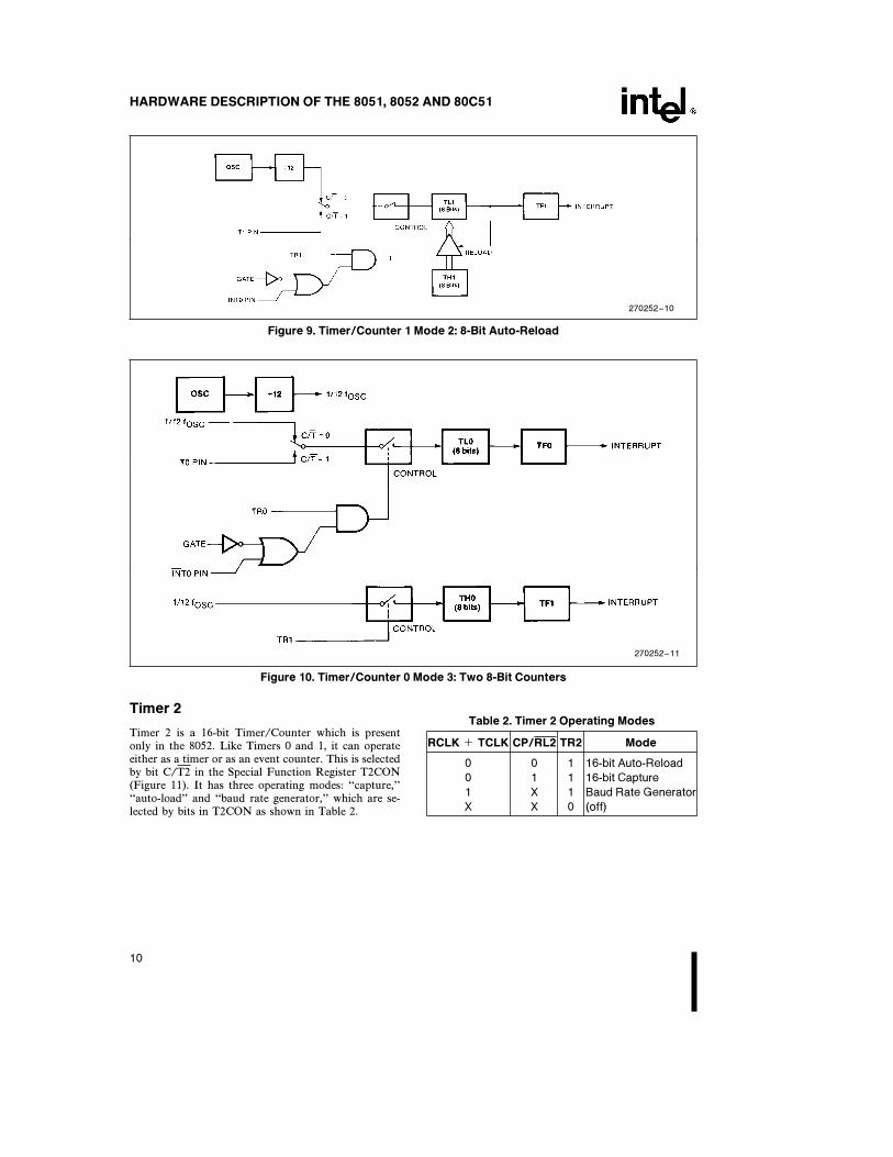
MODE 2
Mode 2 configures the Timer register as an 8-bit Coun-ter (TL1) with automatic reload, as shown in Figure 9.Overflow from TL1 not only sets TF1, but also reloadsTL1 with the contents of TH1, which is preset by soft-ware. The reload leaves TH1 unchanged.
Mode 2 operation is the same for Timer/Counter 0.
MODE 3
Timer 1 in Mode 3 simply holds its count. The effect isthe same as setting TR1 e 0.
Timer 0 in Mode 3 establishes TL0 and TH0 as twoseparate counters. The logic for Mode 3 on Timer 0 isshown in Figure 10. TL0 uses the Timer 0 control bits:C/T, GATE, TR0, INT0, and TF0. TH0 is locked intoa timer function (counting machine cycles) and takesover the use of TR1 and TF1 from Timer 1. Thus, TH0now controls the ‘‘Timer 1’’ interrupt.
Mode 3 is provided for applications requiring an extra8-bit timer or counter. With Timer 0 in Mode 3, an8051 can look like it has three Timer/Counters, and an8052, like it has four. When Timer 0 is in Mode 3,Timer 1 can be turned on and off by switching it out ofand into its own Mode 3, or can still be used by theserial port as a baud rate generator, or in fact, in anyapplication not requiring an interrupt.
9
HARDWARE DESCRIPTION OF THE 8051, 8052 AND 80C51
270252–10
Figure 9. Timer/Counter 1 Mode 2: 8-Bit Auto-Reload
270252–11
Figure 10. Timer/Counter 0 Mode 3: Two 8-Bit Counters
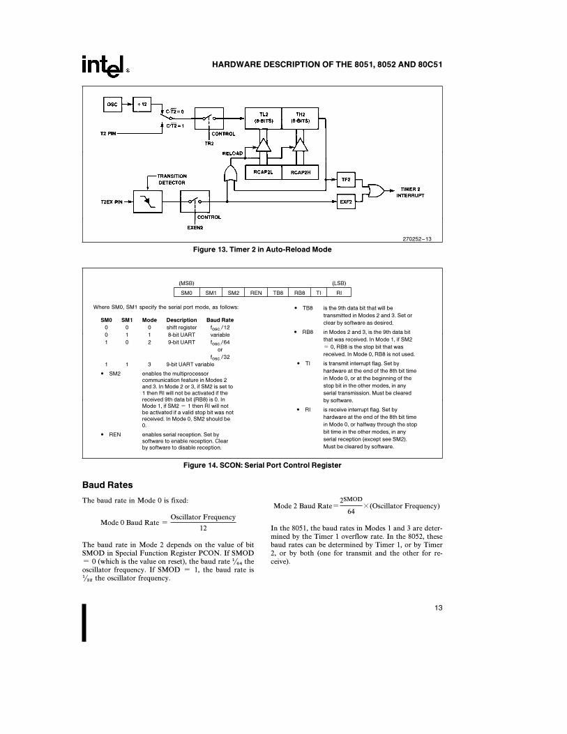
Timer 2
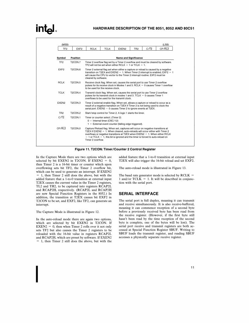
Timer 2 is a 16-bit Timer/Counter which is presentonly in the 8052. Like Timers 0 and 1, it can operateeither as a timer or as an event counter. This is selectedby bit C/T2 in the Special Function Register T2CON(Figure 11). It has three operating modes: ‘‘capture,’’‘‘auto-load’’ and ‘‘baud rate generator,’’ which are se-lected by bits in T2CON as shown in Table 2.
Table 2. Timer 2 Operating Modes
RCLK a TCLK CP/RL2 TR2 Mode
0 0 1 16-bit Auto-Reload
0 1 1 16-bit Capture
1 X 1 Baud Rate Generator
X X 0 (off)
10
HARDWARE DESCRIPTION OF THE 8051, 8052 AND 80C51
(MSB) (LSB)
TF2 EXF2 RCLK TCLK EXEN2 TR2 C/T2 CP/RL2
Symbol Position Name and Significance
TF2 T2CON.7 Timer 2 overflow flag set by a Timer 2 overflow and must be cleared by software.TF2 will not be set when either RCLK e 1 or TCLK e 1.
EXF2 T2CON.6 Timer 2 external flag set when either a capture or reload is caused by a negativetransition on T2EX and EXEN2 e 1. When Timer 2 interrupt is enabled, EXF2 e 1will cause the CPU to vector to the Timer 2 interrupt routine. EXF2 must becleared by software.
RCLK T2CON.5 Receive clock flag. When set, causes the serial port to use Timer 2 overflowpulses for its receive clock in Modes 1 and 3. RCLK e 0 causes Timer 1 overflowto be used for the receive clock.
TCLK T2CON.4 Transmit clock flag. When set, causes the serial port to use Timer 2 overflowpulses for its transmit clock in modes 1 and 3. TCLK e 0 causes Timer 1overflows to be used for the transmit clock.
EXEN2 T2CON.3 Timer 2 external enable flag. When set, allows a capture or reload to occur as aresult of a negative transition on T2EX if Timer 2 is not being used to clock theserial port. EXEN2 e 0 causes Timer 2 to ignore events at T2EX.
TR2 T2CON.2 Start/stop control for Timer 2. A logic 1 starts the timer.
C/T2 T2CON.1 Timer or counter select. (Timer 2)
0 e Internal timer (OSC/12)
1 e External event counter (falling edge triggered).
CP/RL2 T2CON.0 Capture/Reload flag. When set, captures will occur on negative transitions atT2EX if EXEN2 e 1. When cleared, auto-reloads will occur either with Timer 2overflows or negative transitions at T2EX when EXEN2 e 1. When either RCLKe 1 or TCLK e 1, this bit is ignored and the timer is forced to auto-reload onTimer 2 overflow.
Figure 11. T2CON: Timer/Counter 2 Control Register
In the Capture Mode there are two options which areselected by bit EXEN2 in T2CON. If EXEN2 e 0,then Timer 2 is a 16-bit timer or counter which uponoverflowing sets bit TF2, the Timer 2 overflow bit,which can be used to generate an interrupt. If EXEN2e 1, then Timer 2 still does the above, but with theadded feature that a 1-to-0 transition at external inputT2EX causes the current value in the Timer 2 registers,TL2 and TH2, to be captured into registers RCAP2Land RCAP2H, respectively. (RCAP2L and RCAP2Hare new Special Function Registers in the 8052.) Inaddition, the transition at T2EX causes bit EXF2 inT2CON to be set, and EXF2, like TF2, can generate aninterrupt.
The Capture Mode is illustrated in Figure 12.
In the auto-reload mode there are again two options,which are selected by bit EXEN2 in T2CON. IfEXEN2 e 0, then when Timer 2 rolls over it not onlysets TF2 but also causes the Timer 2 registers to bereloaded with the 16-bit value in registers RCAP2Land RCAP2H, which are preset by software. If EXEN2e 1, then Timer 2 still does the above, but with the
added feature that a 1-to-0 transition at external inputT2EX will also trigger the 16-bit reload and set EXF2.
The auto-reload mode is illustrated in Figure 13.
The baud rate generator mode is selected by RCLK e
1 and/or TCLK e 1. It will be described in conjunc-tion with the serial port.
SERIAL INTERFACE
The serial port is full duplex, meaning it can transmitand receive simultaneously. It is also receive-buffered,meaning it can commence reception of a second bytebefore a previously received byte has been read fromthe receive register. (However, if the first byte stillhasn’t been read by the time reception of the secondbyte is complete, one of the bytes will be lost). Theserial port receive and transmit registers are both ac-cessed at Special Function Register SBUF. Writing toSBUF loads the transmit register, and reading SBUFaccesses a physically separate receive register.
11

HARDWARE DESCRIPTION OF THE 8051, 8052 AND 80C51
270252–12
Figure 12. Timer 2 in Capture Mode
The serial port can operate in 4 modes:
Mode 0: Serial data enters and exits through RXD.TXD outputs the shift clock. 8 bits are transmitted/re-ceived: 8 data bits (LSB first). The baud rate is fixed at1/12 the oscillator frequency.
Mode 1: 10 bits are transmitted (through TXD) or re-ceived (through RXD): a start bit (0), 8 data bits (LSBfirst), and a stop bit (1). On receive, the stop bit goesinto RB8 in Special Function Register SCON. Thebaud rate is variable.
Mode 2: 11 bits are transmitted (through TXD) or re-ceived (through RXD): a start bit (0), 8 data bits (LSBfirst), a programmable 9th data bit, and a stop bit (1).On Transmit, the 9th data bit (TB8 in SCON) can beassigned the value of 0 or 1. Or, for example, the paritybit (P, in the PSW) could be moved into TB8. On re-ceive, the 9th data bit goes into RB8 in Special FunctonRegister SCON, while the stop bit is ignored. The baudrate is programmable to either (/32 or (/64 the oscillatorfrequency.
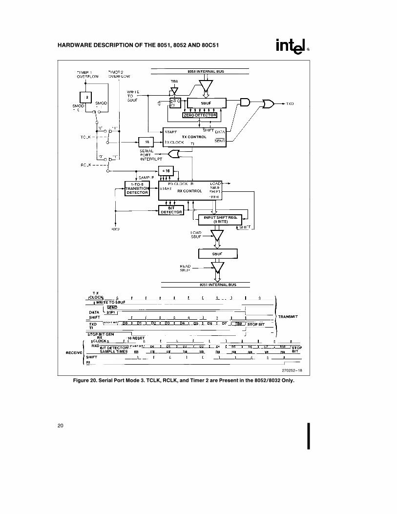
Mode 3: 11 bits are transmitted (through TXD) or re-ceived (through RXD): a start bit (0), 8 data bits (LSBfirst), a programmable 9th data bit and a stop bit (1). Infact, Mode 3 is the same as Mode 2 in all respectsexcept the baud rate. The baud rate in Mode 3 is vari-able.
In all four modes, transmission is initiated by any in-struction that uses SBUF as a destination register. Re-ception is initiated in Mode 0 by the condition RI e 0and REN e 1. Reception is initiated in the othermodes by the incoming start bit if REN e 1.
Multiprocessor Communications
Modes 2 and 3 have a special provision for multipro-cessor communications. In these modes, 9 data bits arereceived. The 9th one goes into RB8. Then comes astop bit. The port can be programmed such that whenthe stop bit is received, the serial port interrupt will beactivated only if RB8 e 1. This feature is enabled bysetting bit SM2 in SCON. A way to use this feature inmultiprocessor systems is as follows.
When the master processor wants to transmit a block ofdata to one of several slaves, it first sends out an ad-dress byte which identifies the target slave. An addressbyte differs from a data byte in that the 9th bit is 1 in anaddress byte and 0 in a data byte. With SM2 e 1, noslave will be interrupted by a data byte. An addressbyte, however, will interrupt all slaves, so that eachslave can examine the received byte and see if it is beingaddressed. The addressed slave will clear its SM2 bitand prepare to receive the data bytes that will be com-ing. The slaves that weren’t being addressed leave theirSM2s set and go on about their business, ignoring thecoming data bytes.
SM2 has no effect in Mode 0, and in Mode 1 can beused to check the validity of the stop bit. In a Mode 1reception, if SM2 e 1, the receive interrupt will not beactivated unless a valid stop bit is received.
Serial Port Control Register
The serial port control and status register is the SpecialFunction Register SCON, shown in Figure 14. Thisregister contains not only the mode selection bits, butalso the 9th data bit for transmit and receive (TB8 andRB8), and the serial port interrupt bits (TI and RI).
12
HARDWARE DESCRIPTION OF THE 8051, 8052 AND 80C51
270252–13
Figure 13. Timer 2 in Auto-Reload Mode
(MSB) (LSB)
SM0 SM1 SM2 REN TB8 RB8 TI RI
Where SM0, SM1 specify the serial port mode, as follows:
SM0 SM1 Mode Description Baud Rate
0 0 0 shift register fosc./12
0 1 1 8-bit UART variable
1 0 2 9-bit UART fosc./64
or
fosc./32
1 1 3 9-bit UART variable
# SM2 enables the multiprocessorcommunication feature in Modes 2and 3. In Mode 2 or 3, if SM2 is set to1 then RI will not be activated if thereceived 9th data bit (RB8) is 0. InMode 1, if SM2 e 1 then RI will notbe activated if a valid stop bit was notreceived. In Mode 0, SM2 should be0.
# REN enables serial reception. Set bysoftware to enable reception. Clearby software to disable reception.
# TB8 is the 9th data bit that will be
transmitted in Modes 2 and 3. Set or
clear by software as desired.
# RB8 in Modes 2 and 3, is the 9th data bit
that was received. In Mode 1, if SM2e 0, RB8 is the stop bit that was
received. In Mode 0, RB8 is not used.
# TI is transmit interrupt flag. Set by
hardware at the end of the 8th bit time
in Mode 0, or at the beginning of the
stop bit in the other modes, in any
serial transmission. Must be cleared
by software.
# RI is receive interrupt flag. Set by
hardware at the end of the 8th bit time
in Mode 0, or halfway through the stop
bit time in the other modes, in any
serial reception (except see SM2).
Must be cleared by software.
Figure 14. SCON: Serial Port Control Register
Baud Rates
The baud rate in Mode 0 is fixed:
Mode 0 Baud Rate e
Oscillator Frequency
12
The baud rate in Mode 2 depends on the value of bitSMOD in Special Function Register PCON. If SMODe 0 (which is the value on reset), the baud rate (/64 theoscillator frequency. If SMOD e 1, the baud rate is(/32 the oscillator frequency.
Mode 2 Baud Ratee
2SMOD
64c(Oscillator Frequency)
In the 8051, the baud rates in Modes 1 and 3 are deter-mined by the Timer 1 overflow rate. In the 8052, thesebaud rates can be determined by Timer 1, or by Timer2, or by both (one for transmit and the other for re-ceive).
13

HARDWARE DESCRIPTION OF THE 8051, 8052 AND 80C51
Using Timer 1 to Generate Baud Rates
When Timer 1 is used as the baud rate generator, thebaud rates in Modes 1 and 3 are determined by theTimer 1 overflow rate and the value of SMOD as fol-lows:
Modes 1, 3Baud Rate e
2SMOD
32c (Timer 1 Overflow Rate)
The Timer 1 interrupt should be disabled in this appli-cation. The Timer itself can be configured for either‘‘timer’’ or ‘‘counter’’ operation, and in any of its 3running modes. In the most typical applications, it isconfigured for ‘‘timer’’ operation, in the auto-reload
mode (high nibble of TMOD e 0010B). In that case,the baud rate is given by the formula
Modes 1, 3Baud Rate e
2SMOD
32c
Oscillator Frequency
12x [256 b (TH1)]
One can achieve very low baud rates with Timer 1 byleaving the Timer 1 interrupt enabled, and configuringthe Timer to run as a 16-bit timer (high nibble ofTMOD e 0001B), and using the Timer 1 interrupt todo a 16-bit software reload.
Figure 15 lists various commonly used baud rates andhow they can be obtained from Timer 1.
Timer 1Baud Rate fOSC SMOD
C/T ModeReloadValue
Mode 0 Max: 1 MHZ 12 MHZ X X X XMode 2 Max: 375K 12 MHZ 1 X X XModes 1, 3: 62.5K 12 MHZ 1 0 2 FFH
19.2K 11.059 MHZ 1 0 2 FDH9.6K 11.059 MHZ 0 0 2 FDH4.8K 11.059 MHZ 0 0 2 FAH2.4K 11.059 MHZ 0 0 2 F4H1.2K 11.059 MHZ 0 0 2 E8H137.5 11.986 MHZ 0 0 2 1DH110 6 MHZ 0 0 2 72H110 12 MHZ 0 0 1 FEEBH
Figure 15. Timer 1 Generated Commonly Used Baud Rates
Using Timer 2 to Generate Baud Rates
In the 8052, Timer 2 is selected as the baud rate genera-tor by setting TCLK and/or RCLK in T2CON (Figure
11). Note then the baud rates for transmit and receivecan be simultaneously different. Setting RCLK and/orTCLK puts Timer 2 into its baud rate generator mode,as shown in Figure 16.
270252–14
Figure 16. Timer 2 in Baud Rate Generator Mode
14
HARDWARE DESCRIPTION OF THE 8051, 8052 AND 80C51
The baud rate generator mode is similar to the auto-re-load mode, in that a rollover in TH2 causes the Timer 2registers to be reloaded with the 16-bit value in registersRCAP2H and RCAP2L, which are preset by software.
Now, the baud rates in Modes 1 and 3 are determinedby Timer 2’s overflow rate as follows:
Modes 1, 3 Baud Rate e
Timer 2 Overflow Rate
16
The Timer can be configured for either ‘‘timer’’ or‘‘counter’’ operation. In the most typical applications, itis configured for ‘‘timer’’ operation (C/T2 e 0). ‘‘Tim-er’’ operation is a little different for Timer 2 when it’sbeing used as a baud rate generator. Normally, as atimer it would increment every machine cycle (thus at(/12 the oscillator frequency). As a baud rate generator,however, it increments every state time (thus at (/2 theoscillator frequency). In that case the baud rate is givenby the formula
Modes 1, 3Baud Rate e
Oscillator Frequency
32x [65536 b (RCAP2H, RCAP2L)]
where (RCAP2H, RCAP2L) is the content ofRCAP2H and RCAP2L taken as a 16-bit unsigned in-teger.
Timer 2 as a baud rate generator is shown in Figure 16.This Figure is valid only if RCLK a TCLK e 1 inT2CON. Note that a rollover in TH2 does not set TF2,and will not generate an interrupt. Therefore, the Timer2 interrupt does not have to be disabled when Timer 2is in the baud rate generator mode. Note too, that ifEXEN2 is set, a 1-to-0 transition in T2EX will setEXF2 but will not cause a reload from (RCAP2H,RCAP2L) to (TH2, TL2). Thus when Timer 2 is in useas a baud rate generator, T2EX can be used as an extraexternal interrupt, if desired.
It should be noted that when Timer 2 is running (TR2e 1) in ‘‘timer’’ function in the baud rate generatormode, one should not try to read or write TH2 or TL2.Under these conditions the Timer is being incrementedevery state time, and the results of a read or write maynot be accurate. The RCAP registers may be read, butshouldn’t be written to, because a write might overlap areload and cause write and/or reload errors. Turn theTimer off (clear TR2) before accessing the Timer 2 orRCAP registers, in this case.
More About Mode 0
Serial data enters and exits through RXD. TXD out-puts the shift clock. 8 bits are transmitted/received: 8data bits (LSB first). The baud rate is fixed at (/12 theoscillator frequency.
Figure 17 shows a simplified functional diagram of theserial port in Mode 0, and associated timing.
Transmission is initiated by any instruction that usesSBUF as a destination register. The ‘‘write to SBUF’’signal at S6P2 also loads a 1 into the 9th position of thetransmit shift register and tells the TX Control block tocommence a transmission. The internal timing is suchthat one full machine cycle will elapse between ‘‘writeto SBUF,’’ and activation of SEND.
SEND enables the output of the shift register to thealternate output function line of P3.0, and also enablesSHIFT CLOCK to the alternate output function line ofP3.1. SHIFT CLOCK is low during S3, S4, and S5 ofevery machine cycle, and high during S6, S1 and S2. AtS6P2 of every machine cycle in which SEND is active,the contents of the transmit shift register are shifted tothe right one position.
As data bits shift out to the right, zeroes come in fromthe left. When the MSB of the data byte is at the outputposition of the shift register, then the 1 that was initial-ly loaded into the 9th position, is just to the left of theMSB, and all positions to the left of that contain zeroes.This condition flags the TX Control block to do onelast shift and then deactivate SEND and set TI. Both ofthese actions occur at S1P1 of the 10th machine cycleafter ‘‘write to SBUF.’’
Reception is initiated by the condition REN e 1 andR1 e 0. At S6P2 of the next machine cycle, the RXControl unit writes the bits 11111110 to the receiveshift register, and in the next clock phase activates RE-CEIVE.
RECEIVE enables SHIFT CLOCK to the alternateoutput function line of P3.1. SHIFT CLOCK makestransitions at S3P1 and S6P1 of every machine cycle.At S6P2 of every machine cycle in which RECEIVE isactive, the contents of the receive shift register are shift-ed to the left one position. The value that comes infrom the right is the value that was sampled at the P3.0pin at S5P2 of the same machine cycle.
As data bits come in from the right, 1s shift out to theleft. When the 0 that was initially loaded into the right-most position arrives at the leftmost position in the shiftregister, it flags the RX Control block to do one lastshift and load SBUF. At S1P1 of the 10th machinecycle after the write to SCON that cleared RI, RE-CEIVE is cleared and RI is set.
More About Mode 1
Ten bits are transmitted (through TXD), or received(through RXD): a start bit (0), 8 data bits (LSB first),and a stop bit (1). On receive, the stop bit goes intoRB8 in SCON. In the 8051 the baud rate is determinedby the Timer 1 overflow rate. In the 8052 it is deter-mined either by the Timer 1 overflow rate, or the Timer2 overflow rate, or both (one for transmit and the otherfor receive).
Figure 18 shows a simplified functional diagram of theserial port in Mode 1, and associated timings for trans-mit receive.
15
HARDWARE DESCRIPTION OF THE 8051, 8052 AND 80C51
270252–15
Figure 17. Serial Port Mode 0
16
HARDWARE DESCRIPTION OF THE 8051, 8052 AND 80C51
270252–16
Figure 18. Serial Port Mode 1. TCLK, RCLK and Timer 2 are Present in the 8052/8032 Only.
Transmission is initiated by any instruction that usesSBUF as a destination register. The ‘‘write to SBUF’’signal also loads a 1 into the 9th bit position of thetransmit shift register and flags the TX Control unitthat a transmission is requested. Transmission actuallycommences at S1P1 of the machine cycle following thenext rollover in the divide-by-16 counter. (Thus, the bit
times are synchronized to the divide-by-16 counter, notto the ‘‘write to SBUF’’ signal).
The transmission begins with activation of SEND,which puts the start bit at TXD. One bit time later,DATA is activated, which enables the output bit of thetransmit shift register to TXD. The first shift pulse oc-curs one bit time after that.
17
HARDWARE DESCRIPTION OF THE 8051, 8052 AND 80C51
As data bits shift out to the right, zeroes are clocked infrom the left. When the MSB of the data byte is at theoutput position of the shift register, then the 1 that wasinitially loaded into the 9th position is just to the left ofthe MSB, and all positions to the left of that containzeroes. This condition flags the TX Control unit to doone last shift and then deactivate SEND and set TI.This occurs at the 10th divide-by-16 rollover after‘‘write to SBUF.’’
Reception is initiated by a detected 1-to-0 transition atRXD. For this purpose RXD is sampled at a rate of 16times whatever baud rate has been established. When atransition is detected, the divide-by-16 counter is imme-diately reset, and 1FFH is written into the input shiftregister. Resetting the divide-by-16 counter aligns itsrollovers with the boundaries of the incoming bit times.
The 16 states of the counter divide each bit time into16ths. At the 7th, 8th, and 9th counter states of each bittime, the bit detector samples the value of RXD. Thevalue accepted is the value that was seen in at least 2 ofthe 3 samples. This is done for noise rejection. If thevalue accepted during the first bit time is not 0, thereceive circuits are reset and the unit goes back to look-ing for another 1-to-0 transition. This is to provide re-jection of false start bits. If the start bit proves valid, itis shifted into the input shift register, and reception ofthe rest of the frame will proceed.
As data bits come in from the right, 1s shift out to theleft. When the start bit arrives at the leftmost positionin the shift register, (which in mode 1 is a 9-bit regis-ter), it flags the RX Control block to do one last shift,load SBUF and RB8, and set RI. The signal to loadSBUF and RB8, and to set RI, will be generated if, andonly if, the following conditions are met at the time thefinal shift pulse is generated.
1) RI e 0, and2) Either SM2 e 0, or the received stop bit e 1
If either of these two conditions is not met, the receivedframe is irretrievably lost. If both conditions are met,the stop bit goes into RB8, the 8 data bits go intoSBUF, and RI is activated. At this time, whether theabove conditions are met or not, the unit goes back tolooking for a 1-to-0 transition in RXD.
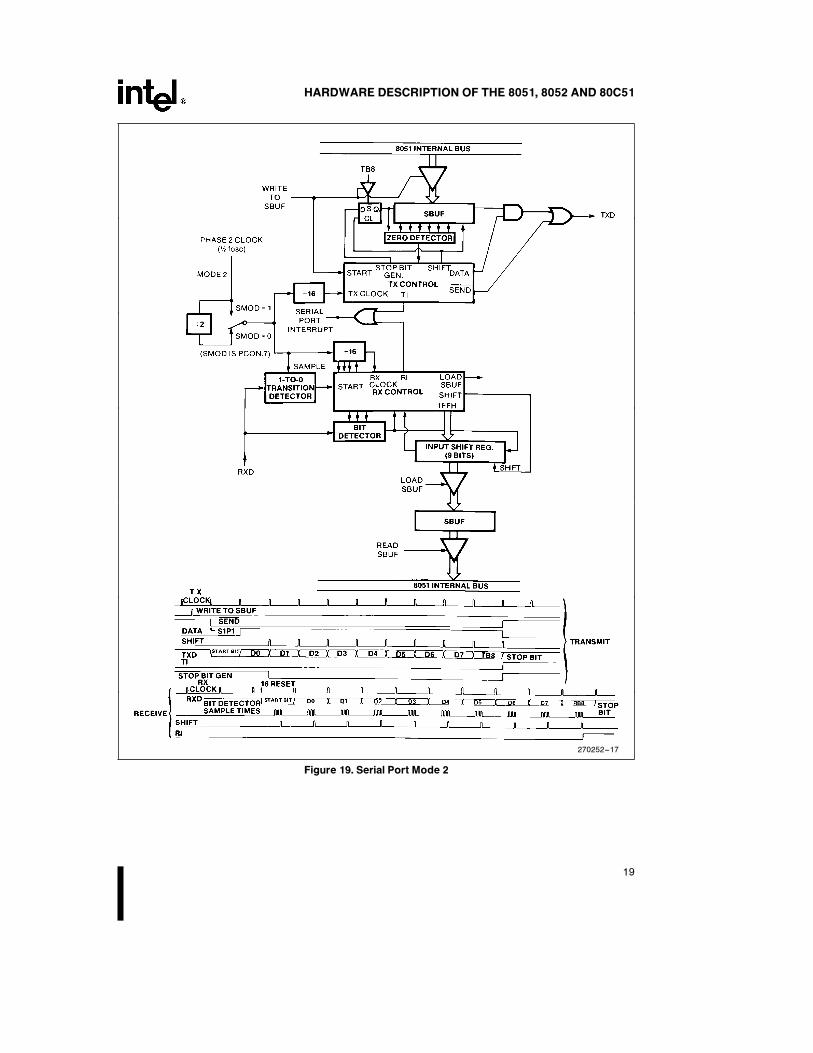
More About Modes 2 and 3
Eleven bits are transmitted (through TXD), or received(through RXD): a start bit (0), 8 data bits (LSB first), aprogrammable 9th data bit, and a stop bit (1). On trans-
mit, the 9th data bit (TB8) can be assigned the value of0 or 1. On receive, the 9th data bit goes into RB8 inSCON. The baud rate is programmable to either (/32 or(/64 the oscillator frequency in Mode 2. Mode 3 mayhave a variable baud rate generated from either Timer 1or 2 depending on the state of TCLK and RCLK.
Figures 19 and 20 show a functional diagram of theserial port in Modes 2 and 3. The receive portion isexactly the same as in Mode 1. The transmit portiondiffers from Mode 1 only in the 9th bit of the transmitshift register.
Transmission is initiated by any instruction that usesSBUF as a destination register. The ‘‘write to SBUF’’signal also loads TB8 into the 9th bit position of thetransmit shift register and flags the TX Control unitthat a transmission is requested. Transmission com-mences at S1P1 of the machine cycle following the nextrollover in the divide-by-16 counter. (Thus, the bittimes are synchronized to the divide-by-16 counter, notto the ‘‘write to SBUF’’ signal.)
The transmission begins with activation of SEND,which puts the start bit at TXD. One bit time later,DATA is activated, which enables the output bit of thetransmit shift register to TXD. The first shift pulse oc-curs one bit time after that. The first shift clocks a 1(the stop bit) into the 9th bit position of the shift regis-ter. Thereafter, only zeroes are clocked in. Thus, asdata bits shift out to the right, zeroes are clocked infrom the left. When TB8 is at the output position of theshift register, then the stop bit is just to the left of TB8,and all positions to the left of that contain zeroes. Thiscondition flags the TX Control unit to do one last shiftand then deactivate SEND and set TI. This occurs atthe 11th divide-by-16 rollover after ‘‘write to SBUF.’’
Reception is initiated by a detected 1-to-0 transition atRXD. For this purpose RXD is sampled at a rate of 16times whatever baud rate has been established. When atransition is detected, the divide-by-16 counter is imme-diately reset, and 1FFH is written to the input shiftregister.
At the 7th, 8th and 9th counter states of each bit time,the bit detector samples the value of RXD. The valueaccepted is the value that was seen in at least 2 of the 3samples. If the value accepted during the first bit timeis not 0, the receive circuits are reset and the unit goesback to looking for another 1-to-0 transition. If thestart bit proves valid, it is shifted into the input shiftregister, and reception of the rest of the frame will pro-ceed.
18
HARDWARE DESCRIPTION OF THE 8051, 8052 AND 80C51
270252–17
Figure 19. Serial Port Mode 2
19
HARDWARE DESCRIPTION OF THE 8051, 8052 AND 80C51
270252–18
Figure 20. Serial Port Mode 3. TCLK, RCLK, and Timer 2 are Present in the 8052/8032 Only.
20
HARDWARE DESCRIPTION OF THE 8051, 8052 AND 80C51
As data bits come in from the right, 1s shift out to theleft. When the start bit arrives at the leftmost positionin the shift register (which in Modes 2 and 3 is a 9-bitregister), it flags the RX Control block to do one lastshift, load SBUF and RB8, and set RI. The signal toload SBUF and RB8, and to set RI, will be generated if,and only if, the following conditions are met at the timethe final shift pulse is generated:
1) RI e 0, and2) Either SM2 e 0 or the received 9th data bit e 1
If either of these conditions is not met, the receivedframe is irretrievably lost, and RI is not set. If bothconditions are met, the received 9th data bit goes intoRB8, and the first 8 data bits go into SBUF. One bittime later, whether the above conditions were met ornot, the unit goes back to looking for a 1-to-0 transitionat the RXD input.
Note that the value of the received stop bit is irrelevantto SBUF, RB8, or RI.
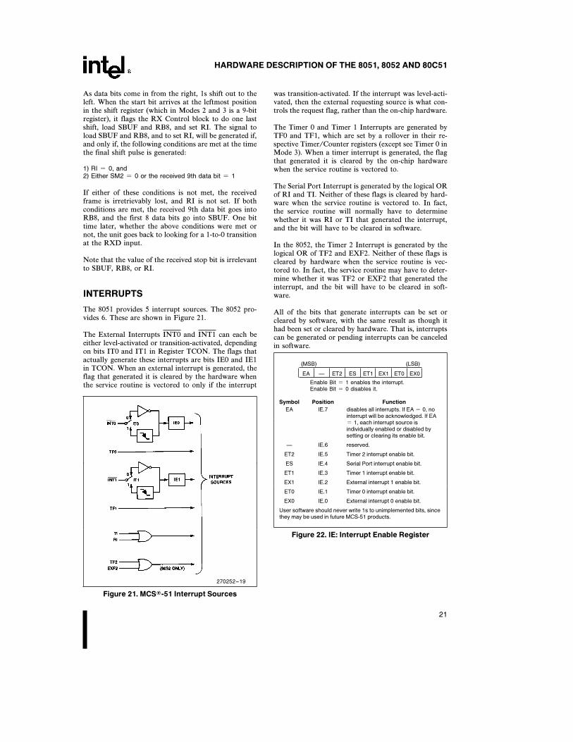
INTERRUPTS
The 8051 provides 5 interrupt sources. The 8052 pro-vides 6. These are shown in Figure 21.
The External Interrupts INT0 and INT1 can each beeither level-activated or transition-activated, dependingon bits IT0 and IT1 in Register TCON. The flags thatactually generate these interrupts are bits IE0 and IE1in TCON. When an external interrupt is generated, theflag that generated it is cleared by the hardware whenthe service routine is vectored to only if the interrupt
270252–19
Figure 21. MCSÉ-51 Interrupt Sources
was transition-activated. If the interrupt was level-acti-vated, then the external requesting source is what con-trols the request flag, rather than the on-chip hardware.
The Timer 0 and Timer 1 Interrupts are generated byTF0 and TF1, which are set by a rollover in their re-spective Timer/Counter registers (except see Timer 0 inMode 3). When a timer interrupt is generated, the flagthat generated it is cleared by the on-chip hardwarewhen the service routine is vectored to.
The Serial Port Interrupt is generated by the logical ORof RI and TI. Neither of these flags is cleared by hard-ware when the service routine is vectored to. In fact,the service routine will normally have to determinewhether it was RI or TI that generated the interrupt,and the bit will have to be cleared in software.
In the 8052, the Timer 2 Interrupt is generated by thelogical OR of TF2 and EXF2. Neither of these flags iscleared by hardware when the service routine is vec-tored to. In fact, the service routine may have to deter-mine whether it was TF2 or EXF2 that generated theinterrupt, and the bit will have to be cleared in soft-ware.
All of the bits that generate interrupts can be set orcleared by software, with the same result as though ithad been set or cleared by hardware. That is, interruptscan be generated or pending interrupts can be canceledin software.
(MSB) (LSB)
EA Ð ET2 ES ET1 EX1 ET0 EX0
Enable Bit e 1 enables the interrupt.Enable Bit e 0 disables it.
Symbol Position Function
EA IE.7 disables all interrupts. If EA e 0, nointerrupt will be acknowledged. If EAe 1, each interrupt source isindividually enabled or disabled bysetting or clearing its enable bit.
Ð IE.6 reserved.
ET2 IE.5 Timer 2 interrupt enable bit.
ES IE.4 Serial Port interrupt enable bit.
ET1 IE.3 Timer 1 interrupt enable bit.
EX1 IE.2 External interrupt 1 enable bit.
ET0 IE.1 Timer 0 interrupt enable bit.
EX0 IE.0 External interrupt 0 enable bit.
User software should never write 1s to unimplemented bits, sincethey may be used in future MCS-51 products.
Figure 22. IE: Interrupt Enable Register
21
HARDWARE DESCRIPTION OF THE 8051, 8052 AND 80C51
Each of these interrupt sources can be individually en-abled or disabled by setting or clearing a bit in SpecialFunction Register IE (Figure 22). IE contains also aglobal disable bit, EA, which disables all interrupts atonce.
Note in Figure 22 that bit position IE.6 is unimple-mented. In the 8051s, bit position IE.5 is also unimple-mented. User software should not write 1s to these bitpositions, since they may be used in future MCS-51products.
Priority Level Structure
Each interrupt source can also be individually pro-grammed to one of two priority levels by setting orclearing a bit in Special Function Register IP (Figure23). A low-priority interrupt can itself be interruptedby a high-priority interrupt, but not by another low-pri-ority interrupt. A high-priority interrupt can’t be inter-rupted by any other interrupt source.
(MSB) (LSB)
Ð Ð PT2 PS PT1 PX1 PT0 PX0
Priority bit e 1 assigns high priority.Priority bit e 0 assigns low priority.
Symbol Position Function
Ð IP.7 reserved
Ð IP.6 reserved
PT2 IP.5 Timer 2 interrupt priority bit.
PS IP.4 Serial Port interrupt priority bit.
PT1 IP.3 Timer 1 interrupt priority bit.
PX1 IP.2 External interrupt 1 priority bit.
PT0 IP.1 Timer 0 interrupt priority bit.
PX0 IP.0 External interrupt 0 priority bit.
User software should never write 1s to unimplemented bits, sincethey may be used in future MCS-51 products.
Figure 23. IP: Interrupt Priority Register
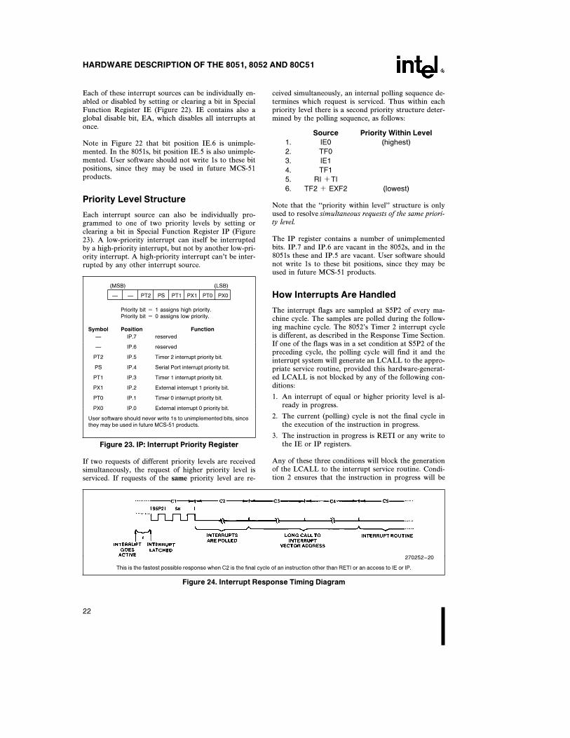
If two requests of different priority levels are receivedsimultaneously, the request of higher priority level isserviced. If requests of the same priority level are re-
ceived simultaneously, an internal polling sequence de-termines which request is serviced. Thus within eachpriority level there is a second priority structure deter-mined by the polling sequence, as follows:
Source Priority Within Level
1. IE0 (highest)
2. TF0
3. IE1
4. TF1
5. RI aTI
6. TF2 a EXF2 (lowest)
Note that the ‘‘priority within level’’ structure is onlyused to resolve simultaneous requests of the same priori-ty level.
The IP register contains a number of unimplementedbits. IP.7 and IP.6 are vacant in the 8052s, and in the8051s these and IP.5 are vacant. User software shouldnot write 1s to these bit positions, since they may beused in future MCS-51 products.
How Interrupts Are Handled
The interrupt flags are sampled at S5P2 of every ma-chine cycle. The samples are polled during the follow-ing machine cycle. The 8052’s Timer 2 interrupt cycleis different, as described in the Response Time Section.If one of the flags was in a set condition at S5P2 of thepreceding cycle, the polling cycle will find it and theinterrupt system will generate an LCALL to the appro-priate service routine, provided this hardware-generat-ed LCALL is not blocked by any of the following con-ditions:
1. An interrupt of equal or higher priority level is al-ready in progress.
2. The current (polling) cycle is not the final cycle inthe execution of the instruction in progress.
3. The instruction in progress is RETI or any write tothe IE or IP registers.
Any of these three conditions will block the generationof the LCALL to the interrupt service routine. Condi-tion 2 ensures that the instruction in progress will be
270252–20
This is the fastest possible response when C2 is the final cycle of an instruction other than RETI or an access to IE or IP.
Figure 24. Interrupt Response Timing Diagram
22
HARDWARE DESCRIPTION OF THE 8051, 8052 AND 80C51
completed before vectoring to any service routine. Con-dition 3 ensures that if the instruction in progress isRETI or any access to IE or IP, then at least one moreinstruction will be executed before any interrupt is vec-tored to.
The polling cycle is repeated with each machine cycle,and the values polled are the values that were present atS5P2 of the previous machine cycle. Note then that ifan interrupt flag is active but not being responded to forone of the above conditions, and is not still active whenthe blocking condition is removed, the denied interruptwill not be serviced. In other words, the fact that theinterrupt flag was once active but not serviced is notremembered. Every polling cycle is new.
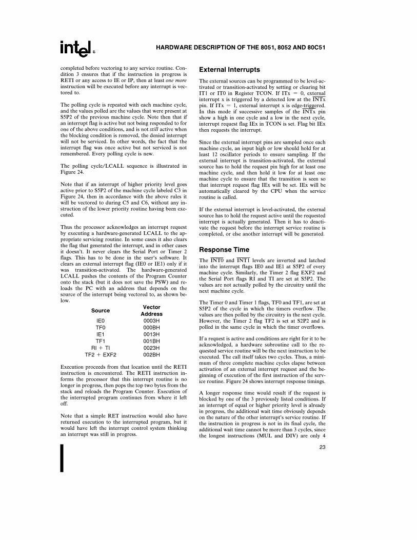
The polling cycle/LCALL sequence is illustrated inFigure 24.
Note that if an interrupt of higher priority level goesactive prior to S5P2 of the machine cycle labeled C3 inFigure 24, then in accordance with the above rules itwill be vectored to during C5 and C6, without any in-struction of the lower priority routine having been exe-cuted.
Thus the processor acknowledges an interrupt requestby executing a hardware-generated LCALL to the ap-propriate servicing routine. In some cases it also clearsthe flag that generated the interrupt, and in other casesit doesn’t. It never clears the Serial Port or Timer 2flags. This has to be done in the user’s software. Itclears an external interrupt flag (IE0 or IE1) only if itwas transition-activated. The hardware-generatedLCALL pushes the contents of the Program Counteronto the stack (but it does not save the PSW) and re-loads the PC with an address that depends on thesource of the interrupt being vectored to, as shown be-low.
SourceVector
Address
IE0 0003H
TF0 000BH
IE1 0013H
TF1 001BH
RI a TI 0023H
TF2 a EXF2 002BH
Execution proceeds from that location until the RETIinstruction is encountered. The RETI instruction in-forms the processor that this interrupt routine is nolonger in progress, then pops the top two bytes from thestack and reloads the Program Counter. Execution ofthe interrupted program continues from where it leftoff.
Note that a simple RET instruction would also havereturned execution to the interrupted program, but itwould have left the interrupt control system thinkingan interrupt was still in progress.
External Interrupts
The external sources can be programmed to be level-ac-tivated or transition-activated by setting or clearing bitIT1 or IT0 in Register TCON. If ITx e 0, externalinterrupt x is triggered by a detected low at the INTxpin. If ITx e 1, external interrupt x is edge-triggered.In this mode if successive samples of the INTx pinshow a high in one cycle and a low in the next cycle,interrupt request flag IEx in TCON is set. Flag bit IExthen requests the interrupt.
Since the external interrupt pins are sampled once eachmachine cycle, an input high or low should hold for atleast 12 oscillator periods to ensure sampling. If theexternal interrupt is transition-activated, the externalsource has to hold the request pin high for at least onemachine cycle, and then hold it low for at least onemachine cycle to ensure that the transition is seen sothat interrupt request flag IEx will be set. IEx will beautomatically cleared by the CPU when the serviceroutine is called.
If the external interrupt is level-activated, the externalsource has to hold the request active until the requestedinterrupt is actually generated. Then it has to deacti-vate the request before the interrupt service routine iscompleted, or else another interrupt will be generated.
Response Time
The INT0 and INT1 levels are inverted and latchedinto the interrupt flags IE0 and IE1 at S5P2 of everymachine cycle. Similarly, the Timer 2 flag EXF2 andthe Serial Port flags RI and TI are set at S5P2. Thevalues are not actually polled by the circuitry until thenext machine cycle.
The Timer 0 and Timer 1 flags, TF0 and TF1, are set atS5P2 of the cycle in which the timers overflow. Thevalues are then polled by the circuitry in the next cycle.However, the Timer 2 flag TF2 is set at S2P2 and ispolled in the same cycle in which the timer overflows.
If a request is active and conditions are right for it to beacknowledged, a hardware subroutine call to the re-quested service routine will be the next instruction to beexecuted. The call itself takes two cycles. Thus, a mini-mum of three complete machine cycles elapse betweenactivation of an external interrupt request and the be-ginning of execution of the first instruction of the serv-ice routine. Figure 24 shows interrupt response timings.
A longer response time would result if the request isblocked by one of the 3 previously listed conditions. Ifan interrupt of equal or higher priority level is alreadyin progress, the additional wait time obviously dependson the nature of the other interrupt’s service routine. Ifthe instruction in progress is not in its final cycle, theadditional wait time cannot be more than 3 cycles, sincethe longest instructions (MUL and DIV) are only 4
23
HARDWARE DESCRIPTION OF THE 8051, 8052 AND 80C51
cycles long, and if the instruction in progress is RETIor an access to IE or IP, the additional wait time can-not be more than 5 cycles (a maximum of one morecycle to complete the instruction in progress, plus 4cycles to complete the next instruction if the instructionis MUL or DIV).
Thus, in a single-interrupt system, the response time isalways more than 3 cycles and less than 9 cycles.
SINGLE-STEP OPERATION
The 8051 interrupt structure allows single-step execu-tion with very little software overhead. As previouslynoted, an interrupt request will not be responded towhile an interrupt of equal priority level is still in prog-ress, nor will it be responded to after RETI until atleast one other instruction has been executed. Thus,once an interrupt routine has been entered, it cannot bere-entered until at least one instruction of the interrupt-ed program is executed. One way to use this feature forsingle-stop operation is to program one of the externalinterrupts (say, INT0) to be level-activated. The serviceroutine for the interrupt will terminate with the follow-ing code:
JNB P3.2,$ ;Wait Here Till INT0 Goes High
JB P3.2,$ ;Now Wait Here Till it Goes Low
RETI :Go Back and Execute One Instruction
Now if the INT0 pin, which is also the P3.2 pin, is heldnormally low, the CPU will go right into the ExternalInterrupt 0 routine and stay there until INT0 is pulsed(from low to high to low). Then it will execute RETI,go back to the task program, execute one instruction,and immediately re-enter the External Interrupt 0 rou-tine to await the next pulsing of P3.2. One step of thetask program is executed each time P3.2 is pulsed.
RESET
The reset input is the RST pin, which is the input to aSchmitt Trigger.
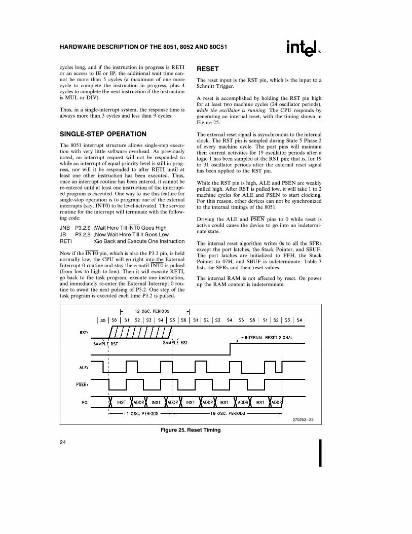
A reset is accomplished by holding the RST pin highfor at least two machine cycles (24 oscillator periods),while the oscillator is running. The CPU responds bygenerating an internal reset, with the timing shown inFigure 25.
The external reset signal is asynchronous to the internalclock. The RST pin is sampled during State 5 Phase 2of every machine cycle. The port pins will maintaintheir current activities for 19 oscillator periods after alogic 1 has been sampled at the RST pin; that is, for 19to 31 oscillator periods after the external reset signalhas been applied to the RST pin.
While the RST pin is high, ALE and PSEN are weaklypulled high. After RST is pulled low, it will take 1 to 2machine cycles for ALE and PSEN to start clocking.For this reason, other devices can not be synchronizedto the internal timings of the 8051.
Driving the ALE and PSEN pins to 0 while reset isactive could cause the device to go into an indetermi-nate state.
The internal reset algorithm writes 0s to all the SFRsexcept the port latches, the Stack Pointer, and SBUF.The port latches are initialized to FFH, the StackPointer to 07H, and SBUF is indeterminate. Table 3lists the SFRs and their reset values.
The internal RAM is not affected by reset. On powerup the RAM content is indeterminate.
270252–33
Figure 25. Reset Timing
24
HARDWARE DESCRIPTION OF THE 8051, 8052 AND 80C51
Table 3. Reset Values of the SFRs
SFR Name Reset Value
PC 0000H
ACC 00H
B 00H
PSW 00H
SP 07H
DPTR 0000H
P0–P3 FFH
IP (8051) XXX00000B
IP (8052) XX000000B
IE (8051) 0XX00000B
IE (8052) 0X000000B
TMOD 00H
TCON 00H
TH0 00H
TL0 00H
TH1 00H
TL1 00H
TH2 (8052) 00H
TL2 (8052) 00H
RCAP2H (8052) 00H
RCAP2L (8052) 00H
SCON 00H
SBUF Indeterminate
PCON (HMOS) 0XXXXXXXB
PCON (CHMOS) 0XXX0000B
270252–21
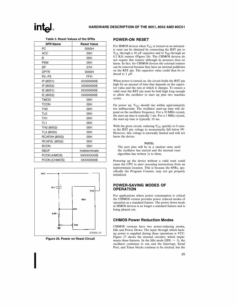
Figure 26. Power on Reset Circuit
POWER-ON RESET
For HMOS devices when VCC is turned on an automat-ic reset can be obtained by connecting the RST pin toVCC through a 10 mF capacitor and to VSS through an8.2 KX resistor (Figure 26). The CHMOS devices donot require this resistor although its presence does noharm. In fact, for CHMOS devices the external resistorcan be removed because they have an internal pulldownon the RST pin. The capacitor value could then be re-duced to 1 mF.
When power is turned on, the circuit holds the RST pinhigh for an amount of time that depends on the capaci-tor value and the rate at which it charges. To ensure avalid reset the RST pin must be held high long enoughto allow the oscillator to start up plus two machinecycles.
On power up, VCC should rise within approximatelyten milliseconds. The oscillator start-up time will de-pend on the oscillator frequency. For a 10 MHz crystal,the start-up time is typically 1 ms. For a 1 MHz crystal,the start-up time is typically 10 ms.
With the given circuit, reducing VCC quickly to 0 caus-es the RST pin voltage to momentarily fall below 0V.However, this voltage is internally limited and will notharm the device.
NOTE:
The port pins will be in a random state untilthe oscillator has started and the internal resetalgorithm has written 1s to them.
Powering up the device without a valid reset couldcause the CPU to start executing instructions from anindeterminate location. This is because the SFRs, spe-cifically the Program Counter, may not get properlyinitialized.
POWER-SAVING MODES OFOPERATION
For applications where power consumption is criticalthe CHMOS version provides power reduced modes ofoperation as a standard feature. The power down modein HMOS devices is no longer a standard feature and isbeing phased out.
CHMOS Power Reduction Modes
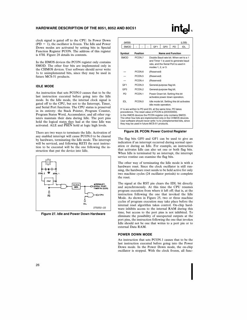
CHMOS versions have two power-reducing modes,Idle and Power Down. The input through which back-up power is supplied during these operations is VCC.Figure 27 shows the internal circuitry which imple-ments these features. In the Idle mode (IDL e 1), theoscillator continues to run and the Interrupt, SerialPort, and Timer blocks continue to be clocked, but the
25
HARDWARE DESCRIPTION OF THE 8051, 8052 AND 80C51
clock signal is gated off to the CPU. In Power Down(PD e 1), the oscillator is frozen. The Idle and PowerDown modes are activated by setting bits in SpecialFunction Register PCON. The address of this registeris 87H. Figure 28 details its contents.
In the HMOS devices the PCON register only containsSMOD. The other four bits are implemented only inthe CHMOS devices. User software should never write1s to unimplemented bits, since they may be used infuture MCS-51 products.
IDLE MODE
An instruction that sets PCON.0 causes that to be thelast instruction executed before going into the Idlemode. In the Idle mode, the internal clock signal isgated off to the CPU, but not to the Interrupt, Timer,and Serial Port functions. The CPU status is preservedin its entirety: the Stack Pointer, Program Counter,Program Status Word, Accumulator, and all other reg-isters maintain their data during Idle. The port pinshold the logical states they had at the time Idle wasactivated. ALE and PSEN hold at logic high levels.
There are two ways to terminate the Idle. Activation ofany enabled interrupt will cause PCON.0 to be clearedby hardware, terminating the Idle mode. The interruptwill be serviced, and following RETI the next instruc-tion to be executed will be the one following the in-struction that put the device into Idle.
270252–22
Figure 27. Idle and Power Down Hardware
(MSB) (LSB)
SMOD - - - GF1 GF0 PD IDL
Symbol Position Name and Function
SMOD PCON.7 Double Baud rate bit. When set to a 1
and Timer 1 is used to generate baud
rate, and the Serial Port is used in
modes 1, 2, or 3.
Ð PCON.6 (Reserved)
Ð PCON.5 (Reserved)
Ð PCON.4 (Reserved)
GF1 PCON.3 General-purpose flag bit.
GF0 PCON.2 General-purpose flag bit.
PD PCON.1 Power Down bit. Setting this bit
activates power down operation.
IDL PCON.0 Idle mode bit. Setting this bit activates
idle mode operation.
If 1s are written to PD and IDL at the same time, PD takesprecedence. The reset value of PCON is (0XXX0000).
In the HMOS devices the PCON register only contains SMOD.The other four bits are implemented only in the CHMOS devices.User software should never write 1s to unimplemented bits, sincethey may be used in future MCS-51 products.
Figure 28. PCON: Power Control Register
The flag bits GF0 and GF1 can be used to give anindication if an interrupt occurred during normal oper-ation or during an Idle. For example, an instructionthat activates Idle can also set one or both flag bits.When Idle is terminated by an interrupt, the interruptservice routine can examine the flag bits.
The other way of terminating the Idle mode is with ahardware reset. Since the clock oscillator is still run-ning, the hardware reset needs to be held active for onlytwo machine cycles (24 oscillator periods) to completethe reset.
The signal at the RST pin clears the IDL bit directlyand asynchronously. At this time the CPU resumesprogram execution from where it left off; that is, at theinstruction following the one that invoked the IdleMode. As shown in Figure 25, two or three machinecycles of program execution may take place before theinternal reset algorithm takes control. On-chip hard-ware inhibits access to the internal RAM during thistime, but access to the port pins is not inhibited. Toeliminate the possibility of unexpected outputs at theport pins, the instruction following the one that invokesIdle should not be one that writes to a port pin or toexternal Data RAM.
POWER DOWN MODE
An instruction that sets PCON.1 causes that to be thelast instruction executed before going into the PowerDown mode. In the Power Down mode, the on-chiposcillator is stopped. With the clock frozen, all func-
26
HARDWARE DESCRIPTION OF THE 8051, 8052 AND 80C51
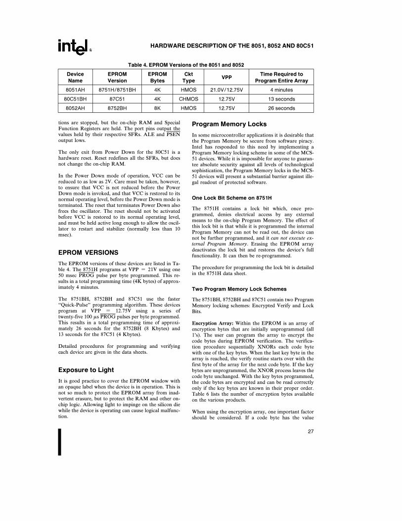
Table 4. EPROM Versions of the 8051 and 8052
Device EPROM EPROM CktVPP
Time Required to
Name Version Bytes Type Program Entire Array
8051AH 8751H/8751BH 4K HMOS 21.0V/12.75V 4 minutes
80C51BH 87C51 4K CHMOS 12.75V 13 seconds
8052AH 8752BH 8K HMOS 12.75V 26 seconds
tions are stopped, but the on-chip RAM and SpecialFunction Registers are held. The port pins output thevalues held by their respective SFRs. ALE and PSENoutput lows.
The only exit from Power Down for the 80C51 is ahardware reset. Reset redefines all the SFRs, but doesnot change the on-chip RAM.
In the Power Down mode of operation, VCC can bereduced to as low as 2V. Care must be taken, however,to ensure that VCC is not reduced before the PowerDown mode is invoked, and that VCC is restored to itsnormal operating level, before the Power Down mode isterminated. The reset that terminates Power Down alsofrees the oscillator. The reset should not be activatedbefore VCC is restored to its normal operating level,and must be held active long enough to allow the oscil-lator to restart and stabilize (normally less than 10msec).
EPROM VERSIONS
The EPROM versions of these devices are listed in Ta-ble 4. The 8751H programs at VPP e 21V using one50 msec PROG pulse per byte programmed. This re-sults in a total programming time (4K bytes) of approx-imately 4 minutes.
The 8751BH, 8752BH and 87C51 use the faster‘‘Quick-Pulse’’ programming algorithm. These devicesprogram at VPP e 12.75V using a series oftwenty-five 100 ms PROG pulses per byte programmed.This results in a total programming time of approxi-mately 26 seconds for the 8752BH (8 Kbytes) and13 seconds for the 87C51 (4 Kbytes).
Detailed procedures for programming and verifyingeach device are given in the data sheets.
Exposure to Light
It is good practice to cover the EPROM window withan opaque label when the device is in operation. This isnot so much to protect the EPROM array from inad-vertent erasure, but to protect the RAM and other on-chip logic. Allowing light to impinge on the silicon diewhile the device is operating can cause logical malfunc-tion.
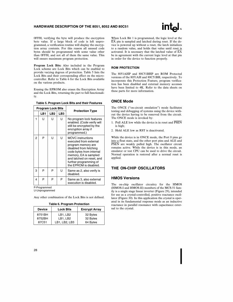
Program Memory Locks
In some microcontroller applications it is desirable thatthe Program Memory be secure from software piracy.Intel has responded to this need by implementing aProgram Memory locking scheme in some of the MCS-51 devices. While it is impossible for anyone to guaran-tee absolute security against all levels of technologicalsophistication, the Program Memory locks in the MCS-51 devices will present a substantial barrier against ille-gal readout of protected software.
One Lock Bit Scheme on 8751H
The 8751H contains a lock bit which, once pro-grammed, denies electrical access by any externalmeans to the on-chip Program Memory. The effect ofthis lock bit is that while it is programmed the internalProgram Memory can not be read out, the device cannot be further programmed, and it can not execute ex-ternal Program Memory. Erasing the EPROM arraydeactivates the lock bit and restores the device’s fullfunctionality. It can then be re-programmed.
The procedure for programming the lock bit is detailedin the 8751H data sheet.
Two Program Memory Lock Schemes
The 8751BH, 8752BH and 87C51 contain two ProgramMemory locking schemes: Encrypted Verify and LockBits.
Encryption Array: Within the EPROM is an array ofencryption bytes that are initially unprogrammed (all1’s). The user can program the array to encrypt thecode bytes during EPROM verification. The verifica-tion procedure sequentially XNORs each code bytewith one of the key bytes. When the last key byte in thearray is reached, the verify routine starts over with thefirst byte of the array for the next code byte. If the keybytes are unprogrammed, the XNOR process leaves thecode byte unchanged. With the key bytes programmed,the code bytes are encrypted and can be read correctlyonly if the key bytes are known in their proper order.Table 6 lists the number of encryption bytes availableon the various products.
When using the encryption array, one important factorshould be considered. If a code byte has the value
27
HARDWARE DESCRIPTION OF THE 8051, 8052 AND 80C51
0FFH, verifying the byte will produce the encryptionbyte value. If a large block of code is left unpro-grammed, a verification routine will display the encryp-tion array contents. For this reason all unused codebytes should be programmed with some value otherthan 0FFH, and not all of them the same value. Thiswill ensure maximum program protection.
Program Lock Bits: Also included in the ProgramLock scheme are Lock Bits which can be enabled toprovide varying degrees of protection. Table 5 lists theLock Bits and their corresponding effect on the micro-controller. Refer to Table 6 for the Lock Bits availableon the various products.
Erasing the EPROM also erases the Encryption Arrayand the Lock Bits, returning the part to full functionali-ty.
Table 5. Program Lock Bits and their Features
Program Lock BitsProtection Type
LB1 LB2 LB3
1 U U U No program lock featuresenabled. (Code verify willstill be encrypted by theencryption array ifprogrammed.)
2 P U U MOVC instructionsexecuted from externalprogram memory aredisabled from fetchingcode bytes from internalmemory, EA is sampledand latched on reset, andfurther programming ofthe EPROM is disabled.
3 P P U Same as 2, also verify isdisabled.
4 P P P Same as 3, also externalexecution is disabled.
P-ProgrammedU-Unprogrammed
Any other combination of the Lock Bits is not defined.
Table 6. Program Protection
Device Lock Bits Encrypt Array
8751BH LB1, LB2 32 Bytes
8752BH LB1, LB2 32 Bytes
87C51 LB1, LB2, LB3 64 Bytes
When Lock Bit 1 is programmed, the logic level at theEA pin is sampled and latched during reset. If the de-vice is powered up without a reset, the latch initializesto a random value, and holds that value until reset isactivated. It is necessary that the latched value of EAbe in agreement with the current logic level at that pinin order for the device to function properly.
ROM PROTECTION
The 8051AHP and 80C51BHP are ROM Protectedversions of the 8051AH and 80C51BH, respectively. Toincorporate this Protection Feature, program verifica-tion has been disabled and external memory accesseshave been limited to 4K. Refer to the data sheets onthese parts for more information.
ONCE Mode
The ONCE (‘‘on-circuit emulation’’) mode facilitatestesting and debugging of systems using the device with-out the device having to be removed from the circuit.The ONCE mode is invoked by:
1. Pull ALE low while the device is in reset and PSENis high;
2. Hold ALE low as RST is deactivated.
While the device is in ONCE mode, the Port 0 pins gointo a float state, and the other port pins and ALE andPSEN are weakly pulled high. The oscillator circuitremains active. While the device is in this mode, anemulator or test CPU can be used to drive the circuit.Normal operation is restored after a normal reset isapplied.
THE ON-CHIP OSCILLATORS
HMOS Versions
The on-chip oscillator circuitry for the HMOS(HMOS-I and HMOS-II) members of the MCS-51 fam-ily is a single stage linear inverter (Figure 29), intendedfor use as a crystal-controlled, positive reactance oscil-lator (Figure 30). In this application the crystal is oper-ated in its fundamental response mode as an inductivereactance in parallel resonance with capacitance exter-nal to the crystal.
28
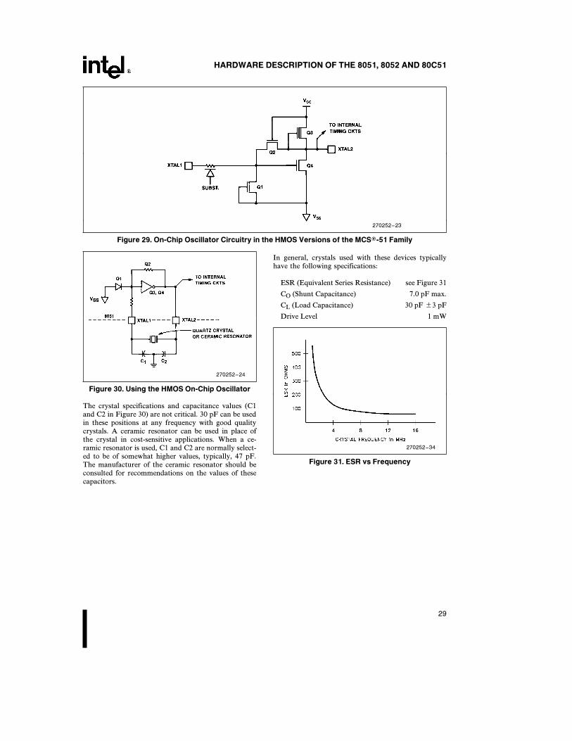
HARDWARE DESCRIPTION OF THE 8051, 8052 AND 80C51
270252–23
Figure 29. On-Chip Oscillator Circuitry in the HMOS Versions of the MCSÉ-51 Family
270252–24
Figure 30. Using the HMOS On-Chip Oscillator
The crystal specifications and capacitance values (C1and C2 in Figure 30) are not critical. 30 pF can be usedin these positions at any frequency with good qualitycrystals. A ceramic resonator can be used in place ofthe crystal in cost-sensitive applications. When a ce-ramic resonator is used, C1 and C2 are normally select-ed to be of somewhat higher values, typically, 47 pF.The manufacturer of the ceramic resonator should beconsulted for recommendations on the values of thesecapacitors.
In general, crystals used with these devices typicallyhave the following specifications:
ESR (Equivalent Series Resistance) see Figure 31
CO (Shunt Capacitance) 7.0 pF max.
CL (Load Capacitance) 30 pF g3 pF
Drive Level 1 mW
270252–34
Figure 31. ESR vs Frequency
29
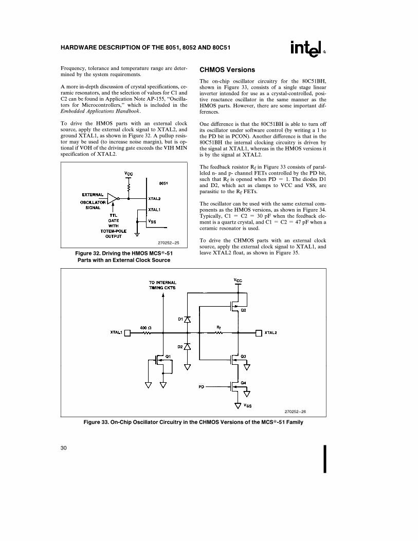
HARDWARE DESCRIPTION OF THE 8051, 8052 AND 80C51
Frequency, tolerance and temperature range are deter-mined by the system requirements.
A more in-depth discussion of crystal specifications, ce-ramic resonators, and the selection of values for C1 andC2 can be found in Application Note AP-155, ‘‘Oscilla-tors for Microcontrollers,’’ which is included in theEmbedded Applications Handbook.
To drive the HMOS parts with an external clocksource, apply the external clock signal to XTAL2, andground XTAL1, as shown in Figure 32. A pullup resis-tor may be used (to increase noise margin), but is op-tional if VOH of the driving gate exceeds the VIH MINspecification of XTAL2.
270252–25
Figure 32. Driving the HMOS MCSÉ-51
Parts with an External Clock Source
CHMOS Versions
The on-chip oscillator circuitry for the 80C51BH,shown in Figure 33, consists of a single stage linearinverter intended for use as a crystal-controlled, posi-tive reactance oscillator in the same manner as theHMOS parts. However, there are some important dif-ferences.
One difference is that the 80C51BH is able to turn offits oscillator under software control (by writing a 1 tothe PD bit in PCON). Another difference is that in the80C51BH the internal clocking circuitry is driven bythe signal at XTAL1, whereas in the HMOS versions itis by the signal at XTAL2.
The feedback resistor Rf in Figure 33 consists of paral-leled n- and p- channel FETs controlled by the PD bit,such that Rf is opened when PD e 1. The diodes D1and D2, which act as clamps to VCC and VSS, areparasitic to the Rf FETs.
The oscillator can be used with the same external com-ponents as the HMOS versions, as shown in Figure 34.Typically, C1 e C2 e 30 pF when the feedback ele-ment is a quartz crystal, and C1 e C2 e 47 pF when aceramic resonator is used.
To drive the CHMOS parts with an external clocksource, apply the external clock signal to XTAL1, andleave XTAL2 float, as shown in Figure 35.
270252–26
Figure 33. On-Chip Oscillator Circuitry in the CHMOS Versions of the MCSÉ-51 Family
30
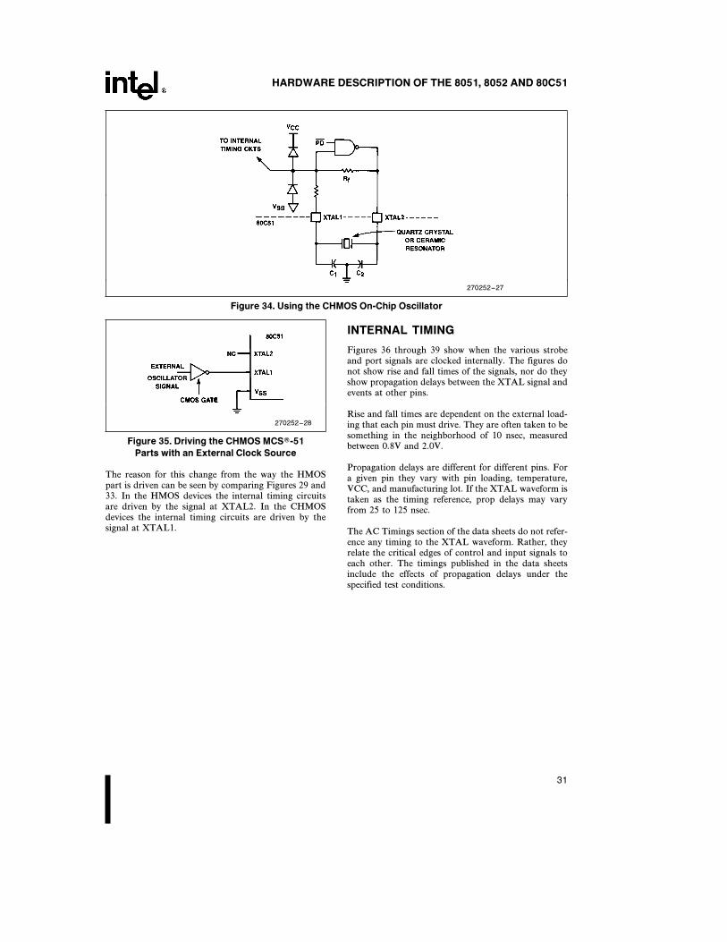
HARDWARE DESCRIPTION OF THE 8051, 8052 AND 80C51
270252–27
Figure 34. Using the CHMOS On-Chip Oscillator
270252–28
Figure 35. Driving the CHMOS MCSÉ-51
Parts with an External Clock Source
The reason for this change from the way the HMOSpart is driven can be seen by comparing Figures 29 and33. In the HMOS devices the internal timing circuitsare driven by the signal at XTAL2. In the CHMOSdevices the internal timing circuits are driven by thesignal at XTAL1.
INTERNAL TIMING
Figures 36 through 39 show when the various strobeand port signals are clocked internally. The figures donot show rise and fall times of the signals, nor do theyshow propagation delays between the XTAL signal andevents at other pins.
Rise and fall times are dependent on the external load-ing that each pin must drive. They are often taken to besomething in the neighborhood of 10 nsec, measuredbetween 0.8V and 2.0V.
Propagation delays are different for different pins. Fora given pin they vary with pin loading, temperature,VCC, and manufacturing lot. If the XTAL waveform istaken as the timing reference, prop delays may varyfrom 25 to 125 nsec.
The AC Timings section of the data sheets do not refer-ence any timing to the XTAL waveform. Rather, theyrelate the critical edges of control and input signals toeach other. The timings published in the data sheetsinclude the effects of propagation delays under thespecified test conditions.
31
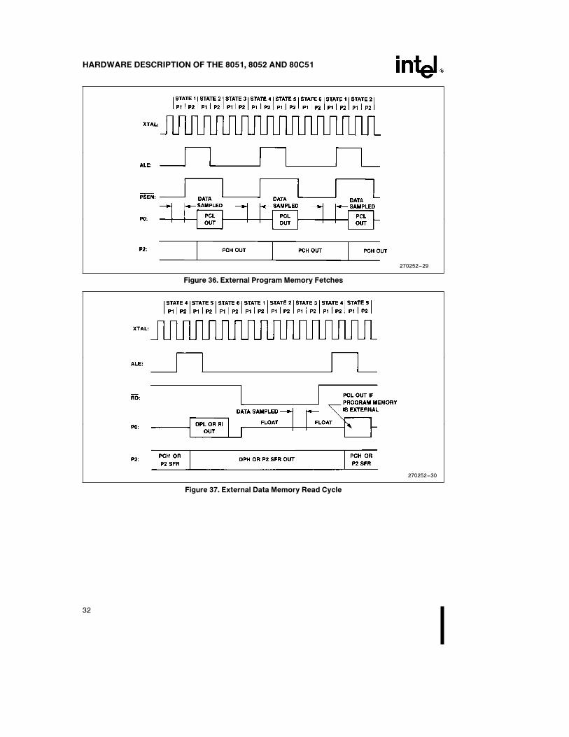
HARDWARE DESCRIPTION OF THE 8051, 8052 AND 80C51
270252–29
Figure 36. External Program Memory Fetches
270252–30
Figure 37. External Data Memory Read Cycle
32
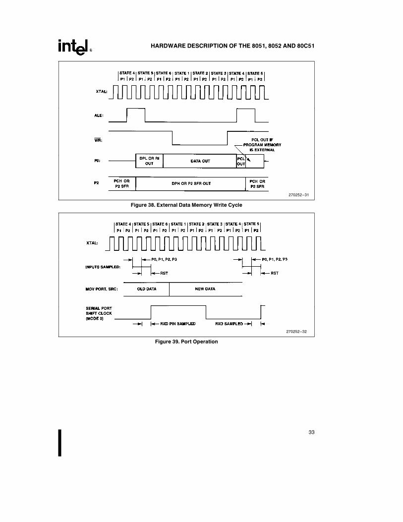
HARDWARE DESCRIPTION OF THE 8051, 8052 AND 80C51
270252–31
Figure 38. External Data Memory Write Cycle
270252–32
Figure 39. Port Operation
33
HARDWARE DESCRIPTION OF THE 8051, 8052 AND 80C51
ADDITIONAL REFERENCES
The following application notes and articles are found in the Embedded Applications handbook.(Order Number: 270648)
1. AP-125 ‘‘Designing Microcontroller Systems for Electrically Noisy Environments’’.
2. AP-155 ‘‘Oscillators for Microcontrollers’’.
3. AP-252 ‘‘Designing with the 80C51BH’’.
4. AR-517 ‘‘Using the 8051 Microcontroller with Resonant Transducers’’.
34