802 ieee transactions on control systems...
TRANSCRIPT

802 IEEE TRANSACTIONS ON CONTROL SYSTEMS TECHNOLOGY, VOL. 15, NO. 5, SEPTEMBER 2007
A Survey of Control Issues in NanopositioningSantosh Devasia, Senior Member, IEEE, Evangelos Eleftheriou, Fellow, IEEE, and
S. O. Reza Moheimani, Senior Member, IEEE
Abstract—Nanotechnology is the science of understandingmatter and the control of matter at dimensions of 100 nm or less.Encompassing nanoscale science, engineering, and technology,nanotechnology involves imaging, measuring, modeling, andmanipulation of matter at this level of precision. An importantaspect of research in nanotechnology involves precision controland manipulation of devices and materials at a nanoscale, i.e.,nanopositioning. Nanopositioners are precision mechatronic sys-tems designed to move objects over a small range with a resolutiondown to a fraction of an atomic diameter. The desired attributesof a nanopositioner are extremely high resolution, accuracy, sta-bility, and fast response. The key to successful nanopositioning isaccurate position sensing and feedback control of the motion. Thispaper presents an overview of nanopositioning technologies anddevices emphasizing the key role of advanced control techniquesin improving precision, accuracy, and speed of operation of thesesystems.
Index Terms—Actuators, atomic force microscopy, nano-posi-tioning, nanotechnology, piezoelectric devices, position sensors,servo control.
I. INTRODUCTION
THE PAST two and a half decades have witnessed theemergence and explosive growth of nanoscience and nan-
otechnology [1]–[4]. The inventions of the scanning tunnelingmicroscope (STM) [5] and the atomic force microscope (AFM)[6] have fundamentally changed research in numerous areas,including biology [7], [8], chemistry [9], materials science[10], [11], and physics [12]. Manipulation and interrogation atthe nanometer scale with a scanning probe microscope (SPM)necessitate positioning systems with atomic-scale resolution[13], [14]. In SPMs, for example, nanopositioning is neededto scan the probe over a sample surface (e.g., during surfaceimaging) and to control the interaction between the probeand the sample surface (e.g., during surface interrogation andmodification). Therefore, further advances in research in allthe above mentioned SPM-based research areas and their wideapplications will depend on the availability of high-precisionnanopositioning stages with increasing bandwidth. Thus, it iswidely recognized that one of the key requirements of nan-otechnology is nanopositioning.
Manuscript received May 17, 2006; revised February 15, 2007 and June 6,2006. Manuscript received in final form June 20, 2007. Recommended by As-sociate Editor K. Turner. The work of S. Devasia was supported in part by theNational Science Foundation under Grant CMS 0301787.
S. Devasia is with the Mechanical Engineering Department, Univer-sity of Washington, Seattle, WA 98195-2600 USA (e-mail: [email protected]).
E. Eleftheriou is with the IBM Zurich Research Laboratory, CH-8803 Rüsch-likon, Switzerland (e-mail: [email protected]).
S. O. R. Moheimani is with the School of Electrical Engineering and Com-puter Science, The University of Newcastle, Callaghan, NSW 2308, Australia(e-mail: [email protected]).
Digital Object Identifier 10.1109/TCST.2007.903345
Nanopositioning systems are also at the core of futurelithography tools that might replace the ubiquitous opticallithography systems [15], [16]—it is not clear whether projec-tion lithography, as used in the production of semiconductorintegrated circuits (ICs), can still be used beyond the 35-nmtechnology node [17]. In general, novel nanopositioning toolsare also needed for the positioning of wafers, mask alignment,and semiconductor inspection systems [17]–[19]. Furthermore,they are vital in molecular biology for imaging, alignment, andnanomanipulation as required, for example, in cell tracking andDNA analysis, nanomaterials testing [20], [21], nanoassembly[22], and the manufacturing of small objects [23]. Such nanopo-sitioning systems are also crucial in optical alignment systems[24], [25] and even in next-generation space telescopes [26],[27]. Finally, nanometer-scale precision will soon be requiredfor the servo system of hard-disk drives (HDD) [28], [29]and for probe-storage devices with areal densities higher than1 Tb/in [30], [31]. This vast range of applications with oper-ation under such diverse conditions poses new challenges forthe control of nanopositioning devices because they necessitatehigh resolution, high bandwidth, and robust control designs,e.g., [32]–[39].
This paper, which reviews the control-related research innanopositioning, is organized as follows. We begin by re-viewing a couple of nanopositioning applications in Section IIto illustrate the control issues. This is followed by an overviewof actuators and sensors used in nanopositioning in Section IIIbefore focusing on the control challenges associated with a spe-cific actuator, i.e., piezoelectric actuators, in Sections IV and V.This focus on piezoelectric actuators is general in the sense thatissues in the control of piezoelectric actuators are similar to theissues with other precision-positioning actuators. This is fol-lowed by a review of current control techniques in Section VI.Separating the control problems and control approaches intotwo sections (Sections V and VI, respectively) allows us toclassify common control paradigms used to resolve some ofthe problems that are unique to nanopositioning such as creepand hysteresis. A review of emerging issues in nanopositioningis provided in Section VII.
II. EXAMPLES OF NANOPOSITIONING APPLICATIONS
In this section, we explain the control issues that arise innanopositioning, using two example applications: scanningprobe microscopy and dual-stage servo systems for HDDs.
A. SPM
Nanopositioning is an important aspect of a huge familyof SPMs that has emerged since the invention of the STMand the AFM [33]–[39]. For example, during AFM imaging,a piezoscanner (based on piezoelectric actuators) changes the
1063-6536/$25.00 © 2007 IEEE

DEVASIA et al.: A SURVEY OF CONTROL ISSUES IN NANOPOSITIONING 803
Fig. 1. AFM probe positioning. A piezoscanner is used to move the samplein the planar x–y axes (parallel to the sample’s substrate) and vertical z-axis(perpendicular to the substrate). Alternatively, the AFM probe can be movedwith a piezoscanner. In some designs, separate piezoscanners are used for thevertical and planar motions.
position of the AFM probe (tip of an AFM-cantilever) relativeto the specimen surface, as shown in Fig. 1.
1) Precision Positioning: Large forces between the AFMprobe and the sample surface can damage the sample or theprobe. To prevent this, the force between the AFM probe and thesample surface is controlled using a feedback loop: First, the ap-plied probe-sample force is estimated by measuring the deflec-tion of the AFM cantilever (which is proportional to the probe-sample force) with optical detectors, e.g., see [40]. Second, themeasured cantilever deflection is used in a feedback loop to ad-just the vertical position of the AFM probe (on the order ofthe instrument’s resolution) such that the cantilever deflection ismaintained at a desired value. Thus, by maintaining a constant(small) cantilever deflection, a constant (small) probe-sampleforce is maintained during imaging. In this sense, precision po-sitioning of the AFM probe is needed to maintain the tip-sampleforce at the desired level during AFM imaging.
2) Obtaining an AFM Image: Changing the vertical posi-tion of the AFM probe to maintain a constant tip-sample inter-action (force) is known as constant force and usually yields afairly faithful topographical image. An image of the sample’stopography is obtained by first raster-scanning the probe overthe sample and then plotting the -displacement of the AFMprobe (estimated using the voltage applied to position theAFM probe in the -direction) against the AFM probe’s –position relative to the substrate on which the sample is placed(see, e.g., [41]). The resulting image resembles an image on atelevision screen in that both consist of many rows or lines ofinformation placed one above the other.
3) Precision Positioning in Other Operating Modes: Othermodes of AFM operation include the tapping mode, whichmaintains a fixed amplitude of oscillation in the AFM can-tilever rather than maintaining a constant force. Moreover,many new variants of SPM exist that allow the measurement oflocal chemical, mechanical (frictional), electric, and magneticproperties of a surface (e.g., [14], [42], [43]). In all of thesevariants, nanopositioning is important to precisely position theSPM probe in close proximity to the sample surface.
Fig. 2. Block diagram of servo system for an example dual-stage HDD. Theerror in head position e over a target data track is used to estimate the positiony of the head. The input U to a VCM and U to a piezoelectric (PZT)actuator are used to position the head at a desired position y . During trackfollow, the position y is maintained over a single data track; during track seek,the goal is to change the position from one data track to another.
4) Increasing the Positioning Bandwidth: SPMs allow sci-entists to image topography or measure the local property of thespecimen under investigation at high resolution, albeit only atrelatively low speed. The low speed is primarily attributed tothe limited bandwidth of the PI-controlled SPM, which is deter-mined by the dynamics of the piezoelectric scanner. High-band-width operation is imperative when imaging the time-varyingnature of the specimen under investigation, e.g., for imagingthe movements of a living cell or the formation of surface fea-tures during materials processing. Lack of high-speed imagingimplies that the resulting AFM images have substantial distor-tions because the sample has changed considerably while theimage was being collected. Therefore, a current challenge inSPM is to achieve the nanopositioning of the SPM probe withhigh bandwidth.
B. Dual-Stage Servo Systems for HDDs
Nanopositioning of the READ-WRITE head over data tracks isbecoming an important issue in HDDs as the data tracks becomesmaller because of the ever increasing areal density of HDDs.Today, a typical track width is on the order of 200 nm, a figurethat is expected to decrease annually by a factor of approxi-mately 30%. A simple rule of thumb for servo design in HDDs isthat three times the statistical standard deviation of the positionerror between the head and the center of the data track shouldbe less than one-tenth of the track width. To achieve these fu-ture ultra-high areal densities, nanometer-level precision of theservo system is required.
1) Precision Positioning: The positioning problem is toplace the READ-WRITE head over a desired spot on the harddisk for recording and retrieving data to and from an HDD (seeFig. 2). Currently, this positioning is achieved by two actuators:a spindle motor that rotates the disk and a voice-coil motor(VCM) that sweeps the head radially over the disk surface. Thehead position relative to the target track center is monitored andadjusted periodically by reading servo information embeddedin the data tracks, using a closed-loop control system that drivesthe VCM actuator. It is noted that a precision positioning servois important to READ and WRITE data at the intended locationon the disk; however, nonlinear friction of the pivot bearinglimits the achievable servo precision. Moreover, the bandwidth

804 IEEE TRANSACTIONS ON CONTROL SYSTEMS TECHNOLOGY, VOL. 15, NO. 5, SEPTEMBER 2007
Fig. 3. Dual-stage servo configurations. Reprinted with permission from [51],© 2003 by ASME. (1) Actuated suspension. (2) Actuated slider. (3) Actuatedhead.
of a traditional single-stage servo system is limited by themultiple mechanical resonances of the actuator as well as byinput-magnitude constraints [44], [45].
2) Dual-Stage Positioning Systems: Dual-stage actuation hasbeen proposed as a solution that would increase both servo band-width and precision [46]–[50]. In such a system, the VCM actsas a first-stage coarse positioner and the microactuator, whichrides on the moving arm of the VCM, is used as a secondaryfine actuator. Note that the second stage is located closer to theREAD-WRITE head (on the moving arm) and has relatively lessmass to move; therefore, it tends to have a higher bandwidththan the VCM. In addition, the second actuator tends to have asignificantly higher positioning precision than the VCM. Thus,the integrated dual-stage system has the large range of the VCMas well as the high precision and large bandwidth of the secondstage.
3) Types of Secondary Actuation: Currently, three maintypes of secondary actuation systems have been proposed:actuated suspension, the actuated slider, and the actuated head(see Fig. 3). In all these configurations, the actuation forcesare generated by piezoelectric, electrostatic, or electromagneticmicroactuators [29], [51]. For example, in the actuated-sus-pension approach, the microactuator is positioned around thesuspension base and actuates the entire suspension (and slider)for head positioning [28], [52], [53]. The advantage of anactuated suspension is that standard fabrication processes canbe used for attaching the piezoelectric secondary actuator tothe base of the suspension; however, a disadvantage is thatthe increase in servo bandwidth is limited by the resonantmodes of the suspension. By moving the microactuator closerto the READ/WRITE element (thereby reducing the mass thatneeds to be moved) the actuated-slider approach, with themicroactuator between the slider and the suspension, results inincreased bandwidth [54], [55]. The microactuator is closestto the READ/WRITE element in actuated-head designs, wherethe microactuator is placed between the slider body and theREAD/WRITE element. One of the most critical challenges ofthis approach is that the actuator fabrication process must becompatible with those of the slider and the head [56].
4) Positioning Control Issues: To introduce this technologyinto commercial products, several aspects still require further re-search, namely, system integration, reliability, and performanceenhancement. Two of the largest commercialization obstaclesto be overcome at this time are the cost and reliability of actu-ated-slider dual-stage servo systems. Other aspects that are the
focus of further research are the dynamic behavior and relia-bility of the microactuator subjected to disturbances due to air-flow, the interaction between head and disk, and the presence ofcontaminants or particles. Future dual-stage servo systems maywell employ an actuated head approach to achieve nanometerservo precision at high bandwidth. Here, research has just begunand it focuses on the key problem of how to combine the fab-rication processes of microactuators and READ/WRITE heads.Also, being investigated is the use of micro-electromechanicalsystems (MEMS) technology to incorporate additional sensors,such as accelerometers and strain gage vibration sensors, to sup-press airflow-induced track miss-registration and external dis-turbances due to mechanical vibrations. Moreover, such a mul-tisensing and multiactuation servo system also requires new,robust, adaptive multiinput–multioutput (MIMO) control archi-tectures and algorithms [29]. Positioning control problems forthe dual-stage system include track seek, where the objectiveis to transition from one track to another, and track follow, i.e.,maintaining the position over a specified track [57]–[59].
III. ACTUATORS AND SENSORS IN NANOPOSITIONING
An important issue in the design of controllers for nanoposi-tioning is the availability and choice of actuators and sensors.Therefore, this section reviews some of the actuators and sen-sors used in nanopositioning.
A. Actuators for Nanopositioning
The main design parameters that characterize the perfor-mance of an actuator are displacement range, force, bandwidth(frequency range), size, weight, and power consumption. Mostactuators usually perform well in some of these categories, buttypically poorly in others. Hence, Section III-A reviews theadvantages and disadvantages of actuation approaches used fornanopositioning.
1) Piezoelectric Actuators: Piezoelectric actuators are ubiq-uitous in nanopositioning applications such as SPMs and micro-motors. They have excellent operating bandwidth and can gen-erate large mechanical forces in a compact design and for smallamounts of power, but they have a relatively small displace-ment range. Bulk ceramic piezoelectric devices based on leadzirconate titanate (PZT) are already well established, but re-cently also thin-film-based devices have started to appear inmany applications [60], [61]. Issues in the modeling and controlof piezoelectric actuators are discussed in Sections IV and V.
2) Magnetostrictive Actuators: In magnetostrictive or piezo-magnetic material, magnetization in an external field which in-duces a dimensional change of the material [62]. Rods of mag-netostrictive materials have found use in the industry in the formof actuators because of their ability to convert electrical energyinto mechanical energy. Typically, current passing through acoil located around a magnetostrictive rod produces the nec-essary magnetic field for actuation. Precision positioning canbe achieved by precise control of the current. This actuationmechanism is important when large forces must be obtainedover small distances. Terfenol-D is a well-known material witha high magnetostriction coefficient that was developed in the1960s. Sputter-deposited magnetostrictive films present an in-teresting opportunity for actuation in micromachines that re-

DEVASIA et al.: A SURVEY OF CONTROL ISSUES IN NANOPOSITIONING 805
Fig. 4. Electrostatic microactuators: (left) interdigitated comb actuator and(right) parallel-plates actuator.
quire contactless high-frequency operation. The power require-ments for magnetostriction are greater than for piezoelectricmaterials, but the actuation offers a larger displacement and theratio of mass per unit stress is greater than with a PZT actuator.As in piezoelectric actuators, control issues in magnetostric-tive actuators include addressing hysteresis effects [63], [64].Another approach with magnetic fields is to levitate an object;nanometer-scale precision is also achievable with such magneticlevitation systems [65].
3) MEMS-Based Electrostatic Actuator: Electrostatic mi-croactuators are well established in the MEMS field because oftheir ease of fabrication as only the structural material needsto be conductive. The electrostatic actuators consist of two in-terdigitated comb structures, one being fixed (the stator), theother movable (the shuttle). An electrical potential applied be-tween the two combs generates a force either in the directionthat increases the overlap of the fingers or in the direction thatincreases the distance between the electrodes, as illustrated inFig. 4. The former is called interdigitated comb actuator, thelatter parallel-plates actuator.
Interdigitated comb and parallel-plates actuators are, in prin-ciple, easy to fabricate—a single mask level and one deep-re-active-ion-etch (DRIE) step suffice to delineate the combs, thetable, the springs, and the frame. For closed-loop position con-trol, the position of the shuttle is determined by measuring thecapacitance across a pair of combs. Electrostatic microactuatorshave been intensively explored as secondary actuators in dual-stage servo systems of HDDs, particularly in the actuated-sliderand actuated-head configurations (see [29] and the referencestherein). They have also been proposed for the medium-actu-ator design of probe-storage devices [66]. Drawbacks of inter-digitated comb drives, however, are the relatively weak forcethey generate and the high voltage they need. For example, fora 50- m motion with 200 fingers, each being 500 m high andspaced 16 m apart, as much as 120 V may have to be applied[66].
4) MEMS-Based Electrostatic Surface Actuator: This typeof actuator (see Fig. 5), which employs a principle similar toa stepper motor [67], also consists of two periodic electrodestructures: one fixed (to the stator) and the other movable (onthe translator). In contrast to an interdigitated comb drive, how-ever, the electrodes are planar and face each other. To move thetranslator to stable positions, in which the periodic structuresare aligned, in-plane forces are generated between them. Theseforces are determined by the spatial phase relationship between
Fig. 5. Electrostatic surface actuator. An example voltage pattern is shown onthe electrodes; the voltage pattern is varied to move the translator.
Fig. 6. Motion cycle of 1-D shuffle actuator [70]. Adapted with permissionfrom [71].
the two sets of periodic electrodes and the voltages applied tothem. For continuous motion, each surface has multiple inter-leaved periodic electrodes that can be successively activated tocreate a voltage wave to move the translator in the desired di-rection. However, this type of actuator also exerts large -axisforces, which must be taken into account in the design of flexuresprings used to hold the translator above the stator.
Here, as in the case of other stepping-type actuators, the posi-tion of the translator is known to within a single step without anindependent position sensor unless the actuation force is over-come by an external force. For an actuator of this type that hasseven addressable periodic electrodes, a position resolution assmall as 5 nm has been achieved [68]. The intrinsic electro-static centering force at each step position acts as a restoringforce. In operation, the overall in-plane stiffness of the trans-lator can be much greater than the stiffness of the flexure springsneeded to hold the translator in place. Accordingly, relativelysoft flexure springs can be used for better power efficiency ifa strong holding force is maintained to counter external dis-turbances. In other actuation systems, this is accomplished viaclosed-loop servo, which, however, requires an independent po-sition sensor and control system [69].
5) MEMS-Based Electrostatic Shuffle Actuator: The shuffleactuator (also known as inchworm actuator) is an electrostaticdesign based on a clamp and slip motion. This design consistsof two feet, independently clamped to the substrate via electro-static force, and a membrane that can be reversibly collapsed byan electrostatic force [70]. Its motion cycle is described in Fig. 6.As the moving element is always clamped by at least one foot,it exhibits high in-plane and out-of-plane rigidity for immunity
806 IEEE TRANSACTIONS ON CONTROL SYSTEMS TECHNOLOGY, VOL. 15, NO. 5, SEPTEMBER 2007
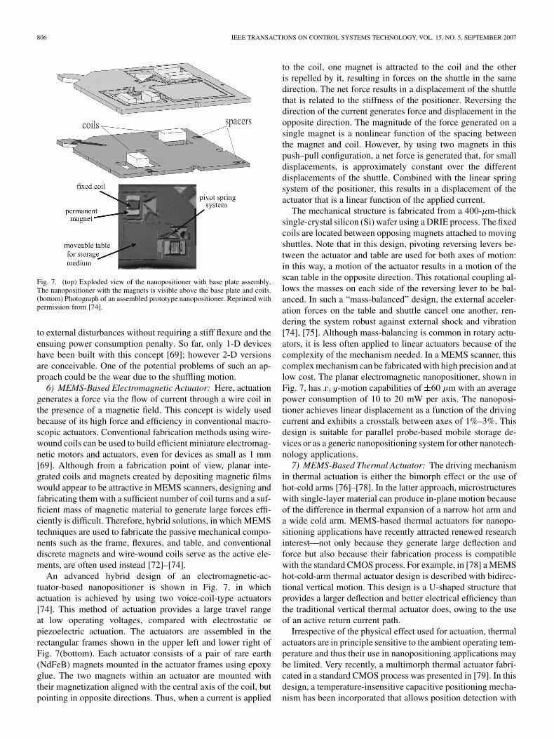
Fig. 7. (top) Exploded view of the nanopositioner with base plate assembly.The nanopositioner with the magnets is visible above the base plate and coils.(bottom) Photograph of an assembled prototype nanopositioner. Reprinted withpermission from [74].
to external disturbances without requiring a stiff flexure and theensuing power consumption penalty. So far, only 1-D deviceshave been built with this concept [69]; however 2-D versionsare conceivable. One of the potential problems of such an ap-proach could be the wear due to the shuffling motion.
6) MEMS-Based Electromagnetic Actuator: Here, actuationgenerates a force via the flow of current through a wire coil inthe presence of a magnetic field. This concept is widely usedbecause of its high force and efficiency in conventional macro-scopic actuators. Conventional fabrication methods using wire-wound coils can be used to build efficient miniature electromag-netic motors and actuators, even for devices as small as 1 mm[69]. Although from a fabrication point of view, planar inte-grated coils and magnets created by depositing magnetic filmswould appear to be attractive in MEMS scanners, designing andfabricating them with a sufficient number of coil turns and a suf-ficient mass of magnetic material to generate large forces effi-ciently is difficult. Therefore, hybrid solutions, in which MEMStechniques are used to fabricate the passive mechanical compo-nents such as the frame, flexures, and table, and conventionaldiscrete magnets and wire-wound coils serve as the active ele-ments, are often used instead [72]–[74].
An advanced hybrid design of an electromagnetic-ac-tuator-based nanopositioner is shown in Fig. 7, in whichactuation is achieved by using two voice-coil-type actuators[74]. This method of actuation provides a large travel rangeat low operating voltages, compared with electrostatic orpiezoelectric actuation. The actuators are assembled in therectangular frames shown in the upper left and lower right ofFig. 7(bottom). Each actuator consists of a pair of rare earth(NdFeB) magnets mounted in the actuator frames using epoxyglue. The two magnets within an actuator are mounted withtheir magnetization aligned with the central axis of the coil, butpointing in opposite directions. Thus, when a current is applied
to the coil, one magnet is attracted to the coil and the otheris repelled by it, resulting in forces on the shuttle in the samedirection. The net force results in a displacement of the shuttlethat is related to the stiffness of the positioner. Reversing thedirection of the current generates force and displacement in theopposite direction. The magnitude of the force generated on asingle magnet is a nonlinear function of the spacing betweenthe magnet and coil. However, by using two magnets in thispush–pull configuration, a net force is generated that, for smalldisplacements, is approximately constant over the differentdisplacements of the shuttle. Combined with the linear springsystem of the positioner, this results in a displacement of theactuator that is a linear function of the applied current.
The mechanical structure is fabricated from a 400- m-thicksingle-crystal silicon (Si) wafer using a DRIE process. The fixedcoils are located between opposing magnets attached to movingshuttles. Note that in this design, pivoting reversing levers be-tween the actuator and table are used for both axes of motion:in this way, a motion of the actuator results in a motion of thescan table in the opposite direction. This rotational coupling al-lows the masses on each side of the reversing lever to be bal-anced. In such a “mass-balanced” design, the external acceler-ation forces on the table and shuttle cancel one another, ren-dering the system robust against external shock and vibration[74], [75]. Although mass-balancing is common in rotary actu-ators, it is less often applied to linear actuators because of thecomplexity of the mechanism needed. In a MEMS scanner, thiscomplex mechanism can be fabricated with high precision and atlow cost. The planar electromagnetic nanopositioner, shown inFig. 7, has -motion capabilities of 60 m with an averagepower consumption of 10 to 20 mW per axis. The nanoposi-tioner achieves linear displacement as a function of the drivingcurrent and exhibits a crosstalk between axes of 1%–3%. Thisdesign is suitable for parallel probe-based mobile storage de-vices or as a generic nanopositioning system for other nanotech-nology applications.
7) MEMS-Based Thermal Actuator: The driving mechanismin thermal actuation is either the bimorph effect or the use ofhot-cold arms [76]–[78]. In the latter approach, microstructureswith single-layer material can produce in-plane motion becauseof the difference in thermal expansion of a narrow hot arm anda wide cold arm. MEMS-based thermal actuators for nanopo-sitioning applications have recently attracted renewed researchinterest—not only because they generate large deflection andforce but also because their fabrication process is compatiblewith the standard CMOS process. For example, in [78] a MEMShot-cold-arm thermal actuator design is described with bidirec-tional vertical motion. This design is a U-shaped structure thatprovides a larger deflection and better electrical efficiency thanthe traditional vertical thermal actuator does, owing to the useof an active return current path.
Irrespective of the physical effect used for actuation, thermalactuators are in principle sensitive to the ambient operating tem-perature and thus their use in nanopositioning applications maybe limited. Very recently, a multimorph thermal actuator fabri-cated in a standard CMOS process was presented in [79]. In thisdesign, a temperature-insensitive capacitive positioning mecha-nism has been incorporated that allows position detection with

DEVASIA et al.: A SURVEY OF CONTROL ISSUES IN NANOPOSITIONING 807
respect to large displacements. The thermal actuator achieveda 24- m displacement with a power consumption of 17 mW.For a closed-loop control bandwidth of 1 kHz, the sensor noisewould limit the minimum detectable signal to 5 nm. So far forthis concept, only a 1-D device has been built; however, 2-Dversions are conceivable.
B. Sensors for Nanopositioning
The speed and absolute positioning accuracy of variousnanopositioning systems crucially depend on the posi-tion-sensing mechanism. On the other hand, generation ofnanometer-scale position information is in itself challenging,particularly in the wide bandwidth and large dynamic rangerequired to achieve a reasonable throughput in many nan-otechnology applications, including lithography and datastorage. Sensors based on a variety of techniques [80], suchas inductive [81], piezoresistive [82], capacitive [29], andoptical measurements [40], [83], [84] are suitable for nanopo-sitioning applications. In this review, we focus on two posi-tion-sensing techniques that are easily integrated with arraysof MEMS-based nanopositioning actuators, namely, capacitiveposition sensing and thermal position sensing. Capacitivesensing is one of the most popular position-sensing techniquesin conjunction with microactuators that achieve nanometerresolution. Very recently, silicon displacement sensors basedon the conduction of heat between two surfaces through theambient air have also demonstrated displacement resolutionsof less than 1 nm.
1) Capacitive Position Sensors: Position transducers basedon capacitive sensing are very popular in the industry becausethey provide a relatively simple technique to implement anoncontact measurement. The principle of capacitive positionsensing is based on the movement of the shuttle electrodethat causes a capacitance change between the fixed (stator)and the movable electrode (shuttle). By measuring the changein capacitance the shuttle location relative to the stator canbe determined. After conversion from capacitance to voltageby means of an electronic circuitry, the capacitance changedue to shuttle movement provides an output voltage that is afunction of the shuttle’s displacement. It can be shown that,for the comb-drive configuration, the output voltage and theshuttle displacement are linearly related. On the other hand, inthe case of the capacitive sensing approach that uses the par-allel-plate drive arrangement, the output voltage and the shuttledisplacement are nonlinearly related. This nonlinear behaviorcan be linearized, to a certain extent, by using a differential par-allel-plate configuration [29]. For electrostatic microactuatorsthat use capacitive sensing for closed- or open-loop positioncontrol, the capacitance variation is on the order of 100 fF/ m[29]. Clearly, to achieve nanometer position resolution, thecircuitry must be able to detect capacitance variations on theorder of 0.1 fF in the presence of parasitic capacitances. It iswell known that for capacitive position sensors the sensingcircuit design is the most critical component.
2) Thermal Position Sensors: The basic design of thethermal position sensor uses a short, elongated U-shaped,free-standing cantilever as shown in Fig. 8(a) [85]. The devices
Fig. 8. (a) Schematic of thermal position sensor. (b) Current flow through theresistive heater results in a rise in temperature of the device. The black arrowsindicate the current path through device. Reprinted with permission from [85],© 2005 IOP Publishing Ltd.
Fig. 9. (a) Heat conduction through the air into the underlying surface. (b) Dis-placement of underlying surface towards the left results in an increase in thecooling efficiency, implying a decrease in the temperature of the heater, whichin turn gives rise to a decrease in its electrical resistance. Reprinted with per-mission from [85], © 2005 IOP Publishing Ltd.
are made from single-crystal Si using standard bulk microma-chining technology. The sensing element is a resistive heatermade from moderately doped Si and supported by legs madefrom highly doped Si that act as electrical leads. Applicationof a voltage across the legs of the device results in a currentflowing through the heater and a subsequent increase in thedevice temperature, as illustrated in Fig. 8(b). To use this deviceas a displacement sensor, it should be positioned directly abovean edge or step on the object of interest, with the long axis ofthe heater aligned parallel to the axis of motion. In addition,the edge should be perpendicular to the direction of motion tobe measured and the surface of the sensor should be parallel tothat of the object of interest, as illustrated in Fig. 9. To sensea displacement of the object, the temperature dependence ofthe Si resistance is exploited. A fraction of the heat generatedby the resistive heater is conducted through the ambient airinto the scan table, which acts as a heat sink. Displacement ofthe scan table gives rise to a change in the efficiency of thiscooling mechanism, resulting in a change in the temperatureof the heater and thus a change in its electrical resistance. Thesensors are driven by a constant voltage, and changes in theresulting current using a current-to-voltage amplifier aremeasured. To minimize drift effects, the sensors are operated inpairs using a differential configuration. Although these devices
808 IEEE TRANSACTIONS ON CONTROL SYSTEMS TECHNOLOGY, VOL. 15, NO. 5, SEPTEMBER 2007
are quite simple, the linearity, noise limit, and drift performancethat can be achieved are surprisingly good. In particular, a dis-placement resolution of less than 1 nm and a dynamic rangeof more than 100 m were achieved in a 10-kHz bandwidth.Power consumption of these devices is on the order of 10 mWper sensor, and the measured time response is described bya simple exponential with a time constant of approximately100 s [85].
IV. PIEZOELECTRIC ACTUATORS FOR NANOPOSITIONING
This section discusses the use of piezoelectric materialsfor the design of nanopositioning actuators. The focus is onpiezoelectric actuators because they are omnipresent in nanopo-sitioning applications, ranging from relatively small-rangenanopositioning stages of SPM to larger-range motors, e.g.,[86] and [87]. Issues in the control of piezoelectric actuators,such as bandwidth and resolution improvements by overcomingactuator dynamics that includes creep, hysteresis nonlinearities,and vibrations, are similar to the issues in other precision-posi-tioning actuators, such as magnetostrictive actuators.
A. Piezoelectric Actuators
The piezoelectric effect was first discovered by the Curiebrothers in 1880 [60], [61]. Specifically, they found thatsqueezing certain materials (piezein is the Greek word forsqueeze) results in an electric charge; this effect enables theuse of piezoelectric materials in strain sensors. However, theuse of piezoelectric materials as actuators exploits the converseeffect, i.e., that the application of an electric voltage results ina mechanical strain. This converse effect is credited to Lipp-mann’s theoretical predictions, which were also experimentallyverified by the Curie brothers. Piezoelectric actuators madeof ceramic PZT have been used for a long time, but recentlythin-film actuators have started to appear in many applications.Historical perspectives of the piezoelectric effect as well asrecent advances in ceramic and thin-film actuators are providedin [60], [61], and [88].
1) Fabrication of Piezoelectric Actuator: A piezoelectric ce-ramic is a mass of perovskite crystals, in which each crystal iscomposed of a small, tetravalent metal ion placed inside a latticeof larger divalent metal ions and O [89]. To prepare a piezo-electric ceramic, fine powders of the component metal oxidesare mixed in specific proportions. This mixture is then heated toform a uniform powder, which in turn is mixed with an organicbinder and formed into specific shapes, e.g., discs, rods, plates,tubes, etc. These elements are then heated for a specific time andunder a predetermined temperature. In this process, the powderparticles sinter and the material forms a dense crystalline struc-ture. The elements are then cooled and, if needed, trimmed intospecific shapes. Finally, silver or copper electrodes are appliedto the appropriate surfaces of the structure.
2) Poling the Piezoelectric Actuator: Above a critical tem-perature, known as the “Curie temperature,” each perovskitecrystal in the heated ceramic element exhibits a simple cubicsymmetry with no dipole moment. However, at temperaturesbelow the Curie temperature, each crystal possesses a dipolemoment. Adjoining dipoles form regions of local alignmentcalled “domains.” This alignment gives a net dipole moment
Fig. 10. Poling process: (a) Prior to polarization polar domains are orientedrandomly. (b) A very large dc electric field is used for polarization. (c) After thedc field is removed, the remnant polarization remains.
to the domain, and thus a net polarization. As demonstratedin Fig. 10(a), the direction of polarization among neighboringdomains is random. Subsequently, the ceramic element has nooverall polarization.
The domains in a ceramic element are aligned by exposingthe element to a strong dc electric field, usually at a temperatureslightly below the Curie temperature [see Fig. 10(b)]. This isreferred to as the “poling process.” After the poling treatment,those domains that are almost aligned with the electric field ex-pand at the expense of domains that are not aligned with thefield and the element expands in the direction of the field. Whenthe electric field is removed, most of the dipoles are locked intoa configuration of near alignment [see Fig. 10(c)]. The elementnow has a permanent polarization, the remnant polarization, andis permanently elongated. The increase in the length of the ele-ment, however, is very small, usually in the micrometer range.
3) Modeling the Piezoelectric Effect: If a poled piezoelectricceramic element is mechanically strained, a resulting electriccharge is produced in the material. This is often referred to asthe “direct piezoelectric effect” and is illustrated in Fig. 11(a).Conversely, application of an electric field to the element re-sults in the material being mechanically strained. This prop-erty is known as “converse piezoelectric effect,” and is shownin Fig. 11(b).
The electromechanical equations for linear piezoelectric ma-terial can be written as (see [90] and [91, Ch. 5])
(1)
(2)
where the indexes and referto different directions within the Cartesian coordinate system,as shown in Fig. 12. The first index refers to the stimuli direc-tion (e.g., electric field), the second shows the direction of re-action (e.g., strain). and correspond to the mechan-ical strain, stress, electrical displacement, and electric field, re-spectively. The material properties , and represent theelastic, piezoelectric strain, and dielectric constants. The secondequation describes the direct and the first the converse piezo-electric effect. By convention, the “3” axis in Fig. 12 is alignedwith the poling direction.
When the applied electric field has the same polarity asthe poling direction, the resulting strain will be positive, whichcorresponds to an elongation, whereas if they are oppositethe resulting stain will be negative, which corresponds to acontraction.

DEVASIA et al.: A SURVEY OF CONTROL ISSUES IN NANOPOSITIONING 809
Fig. 11. Direct and converse piezoelectric effect. (a) Direct effect. (b) Converse effect.
Fig. 12. Right-hand Cartesian coordinate.
For a piezoelectric element, all parameters in (1) and (2) aretensors. However, for objects of certain regular shapes (plates,shells, etc.) these equations can be substantially simplifiedthanks to the geometrical symmetries of these objects andspecific properties of the piezoelectric materials used in theirconstruction [89], [92].
B. Piezoelectric Tube Scanners
The use of piezoelectric tube scanners in SPM was first re-ported in [93]. Compared with traditional tripod positioners,these actuators were found to provide a higher positioning accu-racy and larger bandwidth. In addition, they proved to be easierto manufacture and to integrate into a microscope. Piezoelectrictube scanners are now used extensively in SPM and many otherapplications that involve nanopositioning [36], [94]–[97].
1) Schematic of Positioning Operation: As illustrated inFig. 13, a piezoelectric tube scanner consists of a tube of radi-ally poled piezoelectric material, four external electrodes, and agrounded internal electrode. Opposite electrodes are segmentedin four equal sectors of 90 and driven by signals of identicalmagnitude, but opposite signs. Through bending, this resultsin a 2-D movement in the – plane on, approximately, asphere. In this configuration, the inner electrode is driven by the
-signal. Another configuration includes a circumferential outerelectrode for independent vertical extension or contraction asillustrated in Fig. 1. A drawback of using outer electrodes for
– – movement is that a large scan size reduces the availablerange for -control.
2) Positioning Range: Precise calculation of the scanningrange of a piezoelectric tube can be quite difficult [98]–[100].The bending of the tube is a function of the electric field and the
Fig. 13. Top and side view of a piezoelectric tube scanner with four externalelectrodes and a continuous inner electrode. The bottom end of the tube is fixedand the top end is used for positioning purposes. Equal, but opposite, voltagesare applied to opposite external electrodes to achieve x–y displacement, i.e.,bending of tube. By applying a voltage to the inner electrode z-positioning(elongation of the tube) can be achieved.
induced nonuniform strain. Assuming small deflections, how-ever, would result in the following approximate expression forthe tip translation along the - or -direction [100]
where is the deflection in the - or -direction, is thepiezoelectric strain constant, is the tube length, is the out-side diameter of the tube, is the tube thickness, and is an
- or -axis electrode voltage. The tip deflection can be doubledby applying an equal, but opposite, voltage to the electrodes inthe same axis. Vertical translation due to a voltage applied tothe inner electrode is approximately given by
V. MODELING AND CONTROL ISSUES
Due to the key role played by piezoelectric actuators (e.g.,piezoelectric tubes in SPMs) and the increasing interest in usingmodel-based control design techniques to improve the preci-sion and scanning speed of these devices [33]–[37], [101], [102]interest in understanding the dynamics of these actuators hasincreased. A number of studies have been performed in this
810 IEEE TRANSACTIONS ON CONTROL SYSTEMS TECHNOLOGY, VOL. 15, NO. 5, SEPTEMBER 2007
area, e.g., [103]–[108] and the references therein. The chal-lenges of the modeling and control of piezoelectric actuators arediscussed in this section.
A. Creep
Creep is an undesirable property common with piezoelectricactuators. It can result in significant loss in precision when posi-tioning is required over extended periods of time [109]. In par-ticular, during slow operation of SPMs, creep can result in sig-nificant distortions in the image generated [110].
Piezoelectric creep is related to the effect of the appliedvoltage on the remnant polarization of the piezoceramic ac-tuator. If the operating voltage of a piezoelectric actuator isincreased, the remnant polarization continues to increase. Thismanifests itself in a slow creep after the voltage change iscomplete. A negative step change in the applied voltage wouldhave the opposite effect.
1) Nonlinear Creep Model: A number of approaches havebeen proposed to deal with this phenomenon. One approach isbased on the approximate description of the creep effect by thefollowing nonlinear equation [111]:
(3)
Here, represents the time at which the creep effect is apparent,is the value of the actuator displacement at time , and the
creep rate, , is a fixed value, that can be identified by observingthe step response of the actuator. The use of such a model tocorrect for creep effects is illustrated in [36] and [111].
2) Nonlinear Versus Linear Creep Models: A challenge withthe nonlinear, creep model (3) is its dependence on the choice ofthe time-parameter used to fit the model [111]. For example,the creep rate tends to depend on the choice of the time-pa-rameter . Additionally, for any fixed , the model is not validas time becomes small—the output becomes unbounded as
. Similarly, the output becomes unbounded as time be-comes large, i.e., . These modeling difficulties can bealleviated by using a linear creep model [34] discussed in thefollowing.
3) Linear Creep Model: The linear model proposed in [34]captures the low-frequency response of a piezoelectric actuatorusing creep models applied in mechanics [112]. In particular, thecreep effect can be modeled as a series connection of a numberof springs and dampers [34], i.e.,
(4)
where models the elastic behavior of the actuator at low fre-quencies, is the spring constant, and is the damping con-stant. It has been shown that a model order of three, i.e., ,would capture the creep effect with reasonable accuracy [34].An advantage of this frequency-domain approach is that thislow-frequency model can be appended to the linear model thatdescribes the vibrational dynamics of the actuator at higher fre-quencies. This augmented model can then be used to determinea controller to compensate for creep as well as other adverse vi-bration effects associated with the actuator, as illustrated in [34].
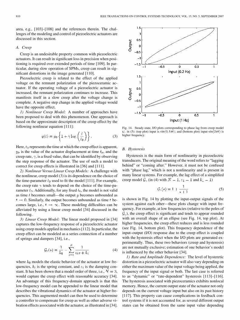
Fig. 14. Steady-state, I/O plots corresponding to phase lag from creep modelG in (5): (top plot) input is sin(0:4�t); and (bottom plot) input sin(2�t) ishigher frequency.
B. Hysteresis
Hysteresis is the main form of nonlinearity in piezoelectrictransducers. The original meaning of the word refers to “laggingbehind” or “coming after.” However, it must not be confusedwith “phase lag,” which is not a nonlinearity and is present inmany linear systems. For example, the lag effect of a simplifiedcreep model (in (4) with and )
(5)
is shown in Fig. 14 by plotting the input-output signals of thesystem against each other—these plots change with input fre-quency. For example, at low frequencies (relative to the poles of
), the creep effect is significant and tends to appear roundedwith an overall shape of an ellipse (see Fig. 14, top plot). Athigher frequencies, the creep effect reduces and is less rounded(see Fig. 14, bottom plot). This frequency dependence of theinput–output (I/O) response due to the creep effect is coupledwith the hysteresis effect when the I/O plots are generated ex-perimentally. Thus, these two behaviors (creep and hysteresis)are not mutually exclusive; estimation of one behavior’s modelis influenced by the other behavior [34].
1) Rate and Amplitude Dependence: The level of hystereticdistortion in a piezoelectric actuator will also vary depending oneither the maximum value of the input voltage being applied, thefrequency of the input signal or both. The last case is referredto as “dynamic” or “rate-dependent” hysteresis [113]–[116].The hysteresis associated with piezoceramics exhibits nonlocalmemory. Hence, the current output state of the actuator not onlydepends on the current voltage input but also on its past history[117]. This property can cause complications in feedback con-trol systems if it is not accounted for, as several different outputstates can be obtained from the same input value depending

DEVASIA et al.: A SURVEY OF CONTROL ISSUES IN NANOPOSITIONING 811
Fig. 15. Example hysteresis loops between input voltage v and the lateralmovement x of an experimental piezoelectric tube.
on the “memory” (or past history) stored in the piezoelectricmaterial.
2) Effect on Closed-Loop Stability: The adverse effect ofhysteresis on the closed-loop stability and performance ofvoltage-controlled piezoelectric actuators has been reported byseveral authors. In particular, [118] reports experimental resultsto illustrate that when a piezoelectric stack actuator is beingused in a feedback loop with a voltage amplifier, the gain andphase margins of the system will deteriorate significantly (upto 28%) owing to the presence of hysteresis.
3) Hysteresis Modeling: To successfully exploit the full po-tential of piezoelectric transducers in control schemes, it is es-sential to understand and model their behavior accurately. Whenthe output is plotted against the input, the plots for increasingand decreasing inputs are different and form a loop (see Fig. 15);early models used polynomials to capture the major loops inthe I/O response, e.g., [119]. However, such approaches fail tocapture the minor loops seen in Fig. 15. The most widely usedapproach to model hysteresis in piezoelectric materials is theclassical Preisach hysteresis model [120]–[123]. Another one isthe Maxwell resistive capacitor (MRC) model [121], [124]. Theconnection between the two approaches has also been investi-gated [125].
The classical Preisach model has been shown to model hys-teresis accurately at a given frequency in many different typesof actuators, such as electromagnets [126], shape memory alloys[127], ferromagnets [128], and piezoceramics [34]. A practicalimplementation of the procedure was described in [120].
4) Modeling the Input-Frequency Dependence: Note that theclassical Preisach approach is not rate-dependent and can onlybe used for applications that operate at a single frequency, suchas SPM. For applications that require a broadband compen-sation, a dynamic Preisach model [114]–[116], [123] must beused instead. An alternative approach is to decouple the linearmodels of creep and vibrations from nonlinear, Preisach modelsof hysteresis [34]. Specifically, hysteresis is modeled as an inputnonlinearity [121] between the applied input voltage and theresulting mechanical input , as shown in Fig. 16. Next, theoutput of this hysteresis submodel is passed through a creepand vibrations submodel [34], which captures the frequency-de-pendant “phase lag” and “oscillations” in the I/O response thatmight otherwise be considered as rate dependence (frequency
Fig. 16. Schematic of piezoelectric actuator model. For an input V , the outputis given by G[H(V )]. The structural vibrations and some of the apparent rate-dependence in the hysteresis effect are captured in a linear model G and thehysteresis nonlinearity H is captured, using, e.g., a rate-independent Preisachhysteresis model.
dependence) in the hysteresis. Interchanging the order of thelinear creep and vibration submodels does not change the input-voltage-to-output-position response of the model.
5) Charge Control Rather Than Voltage Control: Theproblem of controlling the hysteresis effect can be substantiallyeased by the use of charge, or current to drive the piezoelectricactuator. It has been known since the 1980s that the piezoelec-tric effect in a charge-driven piezoelectric actuator is minimal[129], [130]. However, this unique property of piezoelectricmaterials has not been widely used because of the difficultiesassociated with driving highly capacitive loads with availablecharge/current amplifiers. The main problem is the existenceof offset voltages in the charge or current source circuit and theuncontrolled nature of the output voltage, which results in thecapacitive load being charged up. When the output voltage, alsoknown as the compliance voltage, reaches the power supplyrails, the signal applied to the actuator saturates and distortionsoccur. This issue has been pointed out by a number of authors[131], [132]. Recent research [32], [133] proposes a new struc-ture for charge and current sources capable of regulating the dcprofile of the actuator. A dc-accurate charge/current amplifierhas also been proposed in [134] and [135].
C. Vibrations
A major obstacle in achieving high-speed nanopositioning inapplications such as SPM is the vibrations induced when thepositioning bandwidth is increased relative to the first resonantmode of the piezoelectric actuator. This loss of positioning pre-cision is generally small at low operating speeds. Consequently,the operating bandwidth of these systems is restricted to bemuch smaller than the first resonance frequency of the piezo-electric actuator. In applications such as SPM, this amounts toa scanning speed that is 10–100 times lower than the first reso-nance mode of the actuator.
To appreciate the complications that can arise during high-speed nanopositioning applications, note that in SPM a probe ismoved over the sample in a raster pattern. To achieve this spe-cific movement of the probe, a slowly increasing ramp signalis applied to the -electrode of a piezoelectric tube scanner,while the -electrode is driven by a fast triangular waveform.When the frequency of this latter waveform is high, the lateralmovement of the tube is distorted. This situation is illustratedin Fig. 17(top), which depicts the lateral movement of a piezo-electric tube when driven by a 40-Hz signal. The first resonantmode of the tube is located at 850 Hz. The distortions are dueto the amplification of the 21st and 23rd harmonics of the trian-gular waveform, which are close to the first resonant mode of

812 IEEE TRANSACTIONS ON CONTROL SYSTEMS TECHNOLOGY, VOL. 15, NO. 5, SEPTEMBER 2007
Fig. 17. Open-loop (top) and closed-loop (bottom) lateral movement of an ex-perimental piezoelectric tube when driven by a 40-Hz signal. First resonancefrequency of the tube is at 850 Hz. Reprinted from [136] with permission.
the tube. These distortions can be substantially reduced if thisresonant mode is damped. Fig. 17(bottom) illustrates the im-provement that can be achieved if 25-dB damping is added tothe first mode of the structure [136].
D. Modeling Errors
The system performance (controller design) should be robustto the presence of modeling errors due to parameter variationsand unmodeled dynamics.
1) Parameter Variations: A major difficulty in modelingpiezoelectric-actuator dynamics is that parameters (such asthe applied-voltage to induced-strain constant and the externalload) are not known accurately. Therefore, it is challengingto develop a priori accurate models for controller design.Even when the parameters are known, they can change overrelatively long time intervals because of aging effects. More-over, piezoelectric parameters are very sensitive to variationsin temperature [137]. Therefore, experimental modeling andparameter identification are important aspects of the controllerdesign, thus making robust, adaptive, and learning techniqueswell suited for the control of piezoelectric-actuator-basedsystems.
2) Unmodeled Dynamics: When designing controllersfor the vibrational dynamics of piezoelectric actuators, high-frequency vibrational modes are often neglected to obtaina simplified model (for controller design). However, thehigh-frequency vibrational modes can affect the stability ofthe closed-loop system as well as impose limitations on theachievable performance of the closed-loop system. Therefore,the spillover effects on these unmodeled modes should beconsidered in the controller design [138].
3) Coupling Effects: Another type of unmodeled dynamics isthe cross-coupling effect between different axes (e.g., of a piezo-electric tube), which is often assumed to be negligible. However,it has been shown that such effects could become significantif the actuator is used in a high-speed scanning regime [139],[140]. Therefore, there is a need for better understanding cross-
Fig. 18. Tradeoffs between bandwidth, precision, and range.
coupling effects and multiaxis, MIMO controllers in piezoelec-tric tube scanners.
E. Bandwidth-Precision-Range Tradeoffs
Controller design has to consider tradeoffs between the band-width, precision, and range of a piezoelectric actuator, as shownin Fig. 18. Positioning precision depends inversely on the band-width, not only because of the difficulty in controlling higher-frequency modes of the piezoelectric actuator (which leads toa loss in precision), but also because the sensor noise tends tobe proportional to the bandwidth. Moreover, precision also de-pends inversely on the positioning range because of quantiza-tion noise in digital controller implementations. For example,analog-to-digital conversion (when using analog sensors suchas thermal and capacitive sensors) as well as digital-to-analogconversion (for actuation) introduce noise, which adversely af-fects the controller performance.
The bandwidth tends to be inversely dependent on the rangebecause the first vibrational resonance of the piezoelectric actu-ator tends to be higher for a smaller actuator. Note that vibra-tions tend to degrade positioning accuracy as the main frequencycontent of the input becomes close to the first resonance fre-quency of the system. One approach to reduce vibration-inducederror is to choose system inputs that avoid exciting the piezo-electric positioner’s vibrational dynamics. Specifically, vibra-tions can be decreased by limiting the input frequency contentto well below the system resonance (low-speed operation). Al-ternatively, to enable higher-speed operation, the first resonancefrequency of the system can be increased by optimizing the ge-ometry of the piezoelectric positioner (to make it stiffer). Thisoptimization, however, usually results in a smaller (or stiffer)piezoelectric positioner, which also tends to have a smaller max-imum positioning range. Therefore, the tradeoffs are betweenthe maximum range and the achievable bandwidth of the piezo-electric positioner.
VI. CONTROL APPROACHES
This section reviews the literature on controller developmentfor nanopositioning with piezoelectric actuators. The differentapproaches are broadly classified into feedback, feedforward,iterative, and sensorless control.
A. Feedback
1) Integral Controllers: The main advantage of an integralcontroller is that it provides high-gain feedback at low fre-quencies; therefore, integral controllers can overcome creepand hysteresis effects and lead to precision positioning (sincethe vibrational dynamics is not dominant at low frequencies).

DEVASIA et al.: A SURVEY OF CONTROL ISSUES IN NANOPOSITIONING 813
Fig. 19. Feedback control scheme, where the positioner dynamics was modeledin Fig. 16.
In this sense, traditional proportional-integral-derivative (PID)feedback controllers (as shown in Fig. 19), or a double inte-gral for tracking a ramp, are well suited for nanopositioning[141]–[143] and are popular in SPM applications [144]. Re-cently considerable research effort has gone into the automatedtuning of the PID parameters [145] as well as the robustificationof existing integral controllers [37].
2) Low Gain Margin: Precision positioning can also beachieved at high frequencies if feedback controller gains can bechosen to be sufficiently high at those frequencies to overcomevibration-induced errors. Nonetheless, there are limits to theimprovements achievable in positioning performance withhigh-gain controllers because piezoelectric actuators tend tohave low gain margins. The low gain margin is a result of rapidloss in phase at the sharp resonant peak (i.e., first vibrational res-onance) in the frequency response (Bode plots) in combinationwith loss in phase due to higher-frequency dynamics and filtersused with sensors and actuators. Therefore, large feedback gainat high frequency tends to destabilize the piezoscanner [118],[144]. One approach to resolve the low-gain margin problemis to modify the first sharp resonant peak of the system witha notch filter [146], [147]. Experimental results show that thisnotch-filter approach can lead to a marked increase in the gainmargin, and can be used to design feedback controllers that sig-nificantly improve the closed-loop performance in piezoelectricactuators—even at high frequencies [148].
3) Modern Control Techniques: The main challenge in feed-back design is performance improvement while maintainingthe stability of the overall system in the presence of parameteruncertainty and unmodeled high-frequency vibrational modes[138]. Therefore, advanced control techniques have been ap-plied to improve the precision and bandwidth of piezoelectricactuators used in nanopositioning significantly. These controltechniques include state feedback [146], adaptive methods[149], [150], and lead/lag methods [101], [151]. Furthermore,robust control techniques have been developed in [35]–[37],[101] and [102].
B. Feedforward
Use of feedforward can lead to improved output-trackingperformance in SPM [33]. Such feedforward usually augmentsthe feedback controller (see Fig. 20)—the ideal feedforward (toachieve perfect tracking of the desired output, ) is theinverse of the positioner dynamics, inFig. 16.
1) Feedforward Hysteresis Compensation: Several methodshave been proposed to deal with hysteresis in piezoceramics,most of which are based on feedforward inverse compensationschemes, which invert mathematical models of the hysteresis
Fig. 20. Augmenting feedback with feedforward.
nonlinearity ( in Fig. 16) to determine hysteresis-com-pensating inputs. Such hysteresis inverse is sufficient duringlow-frequency operation since creep can be corrected usingfeedback and vibrations are not significant at low frequencies.The inversion is a two-step process. First the hysteresisis fitted with, e.g., polynomials [119], [152], exponentials[153], the Preisach model [117], [126], [154], the MRC model[121], the Prandtle–Ishlinskii model [155], multiple linear-playmodels [156], differential equation models [157], or determin-istic path models [111], [158]. Then, the model is inverted toobtain in a second step. An alternative approach (whichreduces the number of steps) is to directly capture the inversemodel ( , e.g., using a Preisach technique) and use it to findthe input signal [34]. In such feedforward methods, the desiredoutput is fed through the inverse model to obtain the inputsignal, which is then passed onto the physical plant, the outputof which will ideally be the desired signal.
The challenge with such approaches is the modeling com-plexity and parameter sensitivity. Therefore, methods fordealing with hysteresis have been reported that avoid the needfor an accurate model. One such method is the phaser approach,reported in [151] and [159], which essentially represents hys-teresis as a linear phase lag and attempts to compensate for itby using a phase lead transfer function in series with the plant.Describing functions have also been implemented with somesuccess [118], [131].
2) Increasing the Bandwidth: The feedforward methodshown in Fig. 20 does not share the low-gain margin problemof the feedback approach. Therefore, substantial improvementsin precision positioning at high frequency can be achieved byusing feedforward techniques [160]. This ability to increase thebandwidth with model-based feedforward while achieving sub-nanometer-scale positioning precision was first demonstratedexperimentally for an SPM in [33].
Similar to hysteresis compensation, the feedforward ap-proach uses a mathematical model of the system’s lineardynamics ( in Fig. 16) to determine vibration-compensatinginputs for piezoelectric positioners as shown in [33]—thisis augmented with the hysteresis inverse to invert theentire system model as shown in [160]. Recentadvances in inversion methods (to find the feedforward input)can tradeoff actuator limitations with the required positioningprecision [33], [160], [161], exploit actuator redundancy whenusing multiple actuators [81], enable robust inversion of theactuator dynamics [162]–[164], enable online implementationof the inversion approach [165], and reduce the computationaleffort [166].
3) Integration of Feedforward and Feedback: Feedforwardcontrol improves performance without incurring the stabilityproblems associated with feedback design. However, it cannot
814 IEEE TRANSACTIONS ON CONTROL SYSTEMS TECHNOLOGY, VOL. 15, NO. 5, SEPTEMBER 2007
Fig. 21. Inversion-based feedforward of closed-loop system G . The feed-back controller reduces the system nonlinearity and uncertainty; the feedfor-ward is the inverse G of the linearized closed-loop system.
account for modeling errors. In particular, inversion-based feed-forward controllers (which are model-based) cannot correct fortracking errors due to plant uncertainties [167]. Therefore, it isnecessary to use feedback in conjunction with feedforward to re-duce uncertainty-caused errors in the inverse input. Note that theuse of feedforward inputs can improve the tracking performancecompared with the use of feedback alone, even in the presenceof plant uncertainties. The size of acceptable uncertainties toguarantee that performance can only get better by adding feed-forward to feedback has been quantified in [162].
4) Modeling and Computational Complexity: Although thefeedforward input obtained using model-based inversion im-proves positioning precision [34], a challenge in using suchfeedforward methods is the computational effort required to in-vert the piezoelectric-actuator dynamics, which include boththe nonlinear hysteresis effects and the linear vibrational dy-namics. The challenge arises because of the complexity of de-veloping and identifying high-order hysteresis models. More-over, inversion of these high-order models can be computation-ally challenging. Inversion of the linear vibrational dynamicsis relatively simpler [33] than inversion of a nonlinear hystereticsystem with vibrations in Fig. 16.
One approach to reduce the modeling and computationalcomplexity is to first linearize the system by using feedback toovercome the hysteresis effects—issues in the use of high-gainfeedback for linearization are discussed in [148]. Next, thelinearized closed-loop system can be inverted [148], [166],which is easier to invert than the complete nonlinear dynamics,to find the feedforward input (see Fig. 21). While such inver-sion of the closed-loop system leads to reduction in modelingand computational complexity, a drawback of this approach(when compared to the scheme in Fig. 20) is that the achievablepositioning bandwidth (of the closed-loop system ) couldbe limited by the low-gain margin problem in the design of thefeedback controller.
Alternatively, the system nonlinearity can be reduced byusing charge control, and then the inversion-based approach canbe applied to the linearized system to obtain the feedforwardinput [168].
5) Reducing Uncertainty With Feedback: The feedbackcontroller in Fig. 21 can be designed to reduce the uncertaintyin the closed-loop system. This reduces the error in modelingthe closed-loop system , and therefore, reduces the error incomputing the inverse input [148], [166]. Again, a drawback ofthis approach to invert the closed-loop system is that the achiev-able bandwidth is limited by the low-gain margin problem inthe design of the feedback controller. Alternate strategies toreduce uncertainty in the inversion process include: adaptive
inversion of the system model (for both schemes, Figs. 20 and21), see e.g., [169], or learning the correct inverse input thatyields perfect output tracking, i.e., iterative inversion of thesystem model, e.g., [140] and [170].
C. Iterative Control
If the positioning application is repetitive (e.g., periodicscanning of the SPM probe), iterative methods can be used toimprove the positioning performance. Therefore, iterative andadaptive control methods are well suited for nanopositioningapplications.
1) Hysteresis Control: Adaptive and iterative control ap-proaches lead to a reduction in hysteresis effects, and therebyan improvement in positioning precision, e.g., [145], [149],[150], [171], and [172]. A challenge in iterative approachesfor hysteretic systems is to prove convergence of the iterativealgorithm. The difficulty in proving convergence arises be-cause the output is multivalued for a given input (see Fig. 15).Therefore, the direction in which one needs to change the input(i.e., whether to increase or decrease the input to correct anoutput error) cannot be uniquely found [173]. The design ofiterative control algorithms with guaranteed convergence ratesfor piezoelectric actuators has been studied in [173]–[175].
2) Vibration Control: Iterative control can significantlyincrease the operational bandwidth of piezoelectric actuatorswithout loss of positioning precision. For example, in SPMapplications, iterative feedforward approaches can be used toposition the probe precisely over a sample surface [140], [176].Such iterative approaches are particularly useful for precisecontrol of the tip-sample interactions such as the tip-sampleforce to avoid damage of soft biological samples during SPMimaging [140], [176].
D. Sensorless Control
The idea of sensorless control of scan-induced vibrations inpiezoelectric tube scanners is based on the observation that apiezoelectric transducer can function as an actuator, a sensor,or both simultaneously. Exploiting this embedded sensing ca-pability of piezoelectric transducers eliminates the need for anexternal sensor in feedback-based vibration control systems.
1) Piezoelectric Tube Scanners: Two concepts for sensor-less control are illustrated in Fig. 22. In the first approach, illus-trated in Fig. 22(a), one of the electrodes of a piezoelectric tubeis used as a sensor, while the other electrode functions as an ac-tuator. The purpose of the controller is to minimize structuralvibrations of the tube associated with its first resonant mode byadding sufficient damping to the structure. This is a collocatedfeedback control system, and a number of control design tech-niques have been proposed in the literature that are applicablein this case, see, e.g., [177]–[182]. Once sufficient damping hasbeen achieved, tracking can be obtained by driving the systemwith a scanning signal as shown in Fig. 22(a). An application ofthis methodology to a piezoelectric tube scanner is reported in[183]. A downside of this approach is that the scanning rangewould be halved as only one of the electrodes can be used toactuate the tube.
The second concept for sensorless control is illustrated inFig. 22(b) and is generally referred to as piezoelectric shunt

DEVASIA et al.: A SURVEY OF CONTROL ISSUES IN NANOPOSITIONING 815
Fig. 22. Sensorless control of a piezoelectric tube scanner. (a) Strain voltageinduced in one electrode is used as the measurement for feedback controllerK(s) that drives the opposite electrode. (b) One of the electrodes is electricallyshunted to an impedance Z(s).
damping. By shunting one of the electrodes with an appropriateimpedance, structural vibration of the tube can be reduced, andthe opposite electrode can be used to drive the tube with thescanning signal. Although first described in [184], the conceptof piezoelectric shunt damping is usually attributed to Hagoodand von Flotow because of their analysis reported in [185]. A se-ries inductor-resistor network has been demonstrated to reducethe magnitude of a single structural mode significantly. Togetherwith the inherent piezoelectric capacitance of the tube, the net-work is tuned to the resonance frequency of a single structuralmode. Similar to a tuned mechanical absorber, additional dy-namics introduced by the shunt circuit act to increase the effec-tive structural damping [185].
Piezoelectric shunt control has been the subject of intenseresearch, and interesting results have been reported, see [92],[186], [187], and the references therein. In particular, the in-vention of synthetic impedance for the digital implementationof an impedance shunt [188] and the identification of the feed-back structure associated with shunted piezoelectric transducers[189] have enabled researchers to design and implement high-performance shunts in a very effective way. Application of thisconcept to a piezoelectric tube nanopositioner is reported in[135]. An advantage of this approach over collocated feedback,illustrated in Fig. 22(a), is that after a slight modification of theshunt impedance the same shunted electrode can be used to drivethe actuator with the scanning signal [135]. Therefore, the fullscanning range of the nanopositioner can be recovered.
2) Image-Based Sensorless Control: Sensorless controlbecomes important in subnanometer-scale positioning needed
Fig. 23. Image-based STM iterative control [190]. At each iteration step k, theSTM is used to acquire a reference low-speed and a high-speed image (I andI , respectively). These two images are compared to determine the positioningerror e , which is used by the iterative control algorithm (ICA) to determinethe input u for the next iteration step to improve the STM’s positioningaccuracy. (Image provided by Garrett Clayton.)
when imaging surfaces at the atomic scale with a scanningtunneling microscope (STM). One of the difficulties with feed-back approaches in STM is that external sensors cannot directlymeasure the position of an STM-probe’s atomically sharp tip.Instead, they measure the position of a different point on theSTM scanner and then infer the position of the STM-probe’stip. Thus, it is challenging to directly measure the positionof the STM-probe’s tip over the sample surface with externalsensors, also making feedback control challenging.
Moreover, the resolution of conventional sensors is not suffi-cient for feedback control of the STM when subnanometer res-olution is needed at high speeds (at room temperature) becausesensor noise tends to increase with the scan frequency and tem-perature. For example, while the resolution of noncontact ca-pacitive sensors is only limited by quantum noise (in theory),the effective noise factor is about 0.01 nm Hz. Therefore, theresolution becomes poor during high-speed STM operation; theresolution is about 0.1 nm at 100 Hz, which is not sufficient tocorrect for positioning errors when imaging a few carbon atomsin graphite, where the spacing of the atoms is approximately0.2 nm. This lack of high-resolution measurement capabilitiesmakes the use of feedback control to compensate for dynamiceffects in STMs challenging.
To resolve problems with using external sensors, an image-based approach (see Fig. 23) was developed that exploits theextant imaging capability of the STM in [190]. This approach,which uses image distortions to compensate for dynamic effects,extends previously developed methods that have used STM im-ages to correct for positioning errors at relatively low operatingspeeds [191]. The main idea is to quantify the error in posi-tioning the STM-probe’s tip over the sample surface by usingSTM images of standard calibration samples. As the calibra-tion sample surface is fixed, distortions in the image (due to dy-namics effects) can be used to quantify the positioning errorsand correct the input to the STM. In general samples (ratherthan calibration samples), topography-feature recognition canbe used to correct dynamic effects (e.g., to correct creep effects[192]). Thus, the ability to quantify and correct dynamic effectsis only limited by the resolution of the built-in, tunneling-cur-rent sensor (of the STM) and not by limitations of external po-sition sensors. Also, because an image-based approach exploits

816 IEEE TRANSACTIONS ON CONTROL SYSTEMS TECHNOLOGY, VOL. 15, NO. 5, SEPTEMBER 2007
the extant imaging capability of the STM, its use enables an in-creased operating speed without requiring additional hardware,and, therefore, without substantially increasing equipment cost.
An advantage of the image-based approach is that it can beautomated using image-distortion-based error estimation algo-rithms such as those developed in the visual-servoing field (see,for example, [193]). Such automation will make it easy for theend user to not only calibrate, but also recalibrate the STMto account for variations in the scanner dynamics caused bytime-varying effects (e.g., aging-related effects) and operatingconditions (e.g., temperature). Automation will also allow theimage-based approach to be applied to highly parallel micro-fabricated STM systems that are being developed for nanotech-nologies. Such miniaturized arrays have higher bandwidth [194]and increased throughput [195], but their operational speed isstill limited by dynamic effects. Thus, higher-speed operationof such miniaturized parallel systems can also be enabled byexploiting the image-based approach.
VII. EMERGING CONTROL ISSUES
In this section, we will discuss some of the emerging appli-cations and control issues in nanopositioning.
A. Precision Positioning Over Long Range
The need for positioning systems with nanometer-scale pre-cision over extended ranges has typically been given a lowerpriority on the basis that nanotechnologies (such as nanofabri-cation) were purely limited to research [196]. However, long-range high-precision positioning is becoming increasingly crit-ical as we realize the many possibilities nanotechnology has tooffer. For example, such positioning systems are particularlyimportant to bridge the gap between micro- and nanofabricationwhen linking compound geometric patterns containing nanos-tructures with their much larger I/O connections [196]. Cur-rent commercially available inchworm motors offer both highprecision and long range—they are capable of nanometer-pre-cision positioning over the centimeter range (see, e.g., [26],[27], [197], and [198]). However, because of vibrations inducedduring locomotion, the positioning precision of inchworm mo-tors is lost during high-speed operation.
1) Long-Range High-Precision Positioning With InchwormMotors: Inchworm motors are capable of delivering highprecision over long-range motions. As shown in Fig. 24, thepiezoelectric motor is stationary (fixed to the ground at C)while the inner rod travels back and forth. (A kinematic vari-ation is to hold the rod stationary and let the inchworm motormove over the rod.) In such motors, relatively large movementswith nanometer-scale precision can be achieved by repeatinga nanostepping procedure. Briefly, the substeps involved in ananostep movement are as follows (see Fig. 24). First, piezo-electric actuator A clamps to the rod; then piezoelectric actuatorB expands, forcing the rod to move to the left; piezoelectricactuator C clamps and A releases, and finally, B contracts,forcing the rod to move to the left again. This motion, repeatedover and over again, allows the inchworm motor to achievenanometer-precision positioning of the rod over a long range.
Fig. 24. Schematic of an inchworm moving a rod to the left—this requiresrepeated clamping and unclamping of piezoelectric actuators A and C. (a) Aclamps to the rod, (b) B expands, forcing the rod to move to the left, (c) Cclamps and A releases, and (d) B contracts, again forcing the rod to move to theleft.
2) Impact Control in Inchworm Stages: Impact-induced vi-brations that result from each clamping step (piezoelectric ac-tuators A and C) become more and more pronounced with in-creasing operating speed, and lead to loss of positioning pre-cision during high-speed operation. Furthermore, each on–offcycle of a clamp produces dynamic tensile stresses that will ul-timately produce cracks in the piezoelectric material. For ex-ample, the fatigue life of piezoelectric actuators in the inchwormmotor (used by Burleigh Instruments, Inc.) ranges from 100 mil-lion to one billion clamp-change cycles. If the inchworm motortakes nanometer-sized steps, its estimated life is on the order of200 to 2000 m. This estimated life is extremely low if such adevice is to be used for long-range positioning (with nanometerprecision). A typical recommendation to reduce the possibilityof fatigue failure of the piezoelectric actuator (at present) is toavoid mechanical shocks—i.e., to go slow. Therefore, controltechniques are needed to mitigate the adverse effects of impactforces and vibration during rapid positioning with inchwormmotors.
B. Increasing Throughput
The throughput of current SPM-based nanofabrication is toolow to be economically viable. Therefore, a substantial increaseof the throughput is needed.
1) Use of SPM in Nanofabrication: Although SPM was ini-tially developed and applied—with tremendous success—as asurface analysis instrument, its potential for surface and materialmodification is now being exploited for nanofabrication [15].The main advantage of SPM-based nanofabrication is that itachieves the smallest features [15]: For example, STM achievesthe manipulation of single atoms, although in highly restrictiveenvironments [199]. In general, STM can be used for additivenanofabrication by depositing material from a gas precursor (alocalized chemical vapor deposition technique) or from an elec-trolyte (localized electrodeposition). Material can also be re-moved from the substrate by mechanical means such as con-tacting the tip against the sample as in AFM or by electricalpulses. Other approaches, such as localized etching of the sur-face with a gas or electrolyte, also fall under the second category,where material is removed from the substrate. Thus, SPM-based

DEVASIA et al.: A SURVEY OF CONTROL ISSUES IN NANOPOSITIONING 817
techniques are poised to play a significant role in future tech-nological progress, especially when manufacturing processesin electronics, optics, and precision machining begin to requirenanometer-scale control over feature sizes.
2) Low Throughput of SPM-Based Nanofabrication: Unfor-tunately, SPM-based nanofabrication suffers from throughputlimitations present in all serial techniques—the tip must visiteach point where something is to be done. Even with multipleprobes [195], [200] such serial processes cannot compete withparallel techniques like current optical lithography, which canprocess an entire wafer (more precisely, one die) in one step.
3) Integrating Top-Down and Bottom-Up Nanofabrication:One solution to the low-throughput problem is to integrate theslower, top-down, SPM nanofabrication with faster, bottom-up,nanofabrication methods. For example, rather than adding allthe required material in a direct write approach, STM-basedchemical vapor deposition (CVD) might be used only forseeding or prenucleating the desired pattern, whereas the restof the material can then be grown by selective CVD [201].Similarly, patterned self-assembled monolayers can be fabri-cated with AFM-based dip-pen nanolithography, which canthen be used for nucleation and growth of functional polymers[202], [203]. In this sense, the top-down SPM is only neededfor generating the initial pattern, which then forms the basisfor growing the nanostructure using highly-parallel bottom-uptechniques [204], [205].
4) Need for High-Speed Positioning: The generation of ini-tial seed patterns with an SPM will require rapid positioning ofthe SPM probe (i.e., the output) from one location to another onthe initial seed pattern. Therefore, optimal control techniquesand trajectory-planning methods are well suited to rapidly shiftthe SPM probe from one position to another [206], [207]. Sim-ilar methods have also been used to optimize the scan paths inSPMs [208].
C. Distributed Nanopositioning Systems
Distributed arrays of nanopositioners lead to highly parallelsystems, which have both long range as well as high bandwidth.Control of such distributed systems is an emerging area in ap-plications such as data storage and nanofabrication.
1) Storage Application: The ability to modify surfaces withan SPM has motivated efforts to create data-storage devicesbased on scanning-probe techniques for storing data at muchhigher densities than can be achieved by conventional means,e.g., [30] and [209]–[211]. These devices are still based onmechanical access, but MEMS-based actuators, sensors, andmicro-scanners will replace the microscopic actuators, motors,and mechanical structures of conventional storage devices. Itis the unique capabilities of the MEMS structures that promisesmall form factor, low power consumption, fast mechanicalaccess times, and good shock robustness. In such storage de-vices, the rotating disk and single head per surface paradigmsof HDD have been abandoned in favor of MEMS-basedactuators (in some designs -direction actuation is necessary)that position a large 2-D array of probe tips over the storagemedium for parallel READ/WRITE operations. The schematicillustration of an example device is shown in Fig. 25. Asactuation distances are typically on the order of 100 m, and
Fig. 25. Schematic of MEMS-based probe-storage device. (Reprinted with per-mission from [212].)
components have small masses, the positioning delays, i.e.,access times, are much smaller than in disk drives. However,to achieve the ultrahigh storage densities that are possible withscanning probes, extreme precision in navigating the probe tipsto the desired position is required.
2) Design Requirements: Functional storage devices requiremechanical motion between the READ/WRITE probes and thestorage medium. This is accomplished by a microscanner con-sisting of a movable table on which the medium (or alterna-tively, the probe array) is located, a spring system with suffi-cient compliance to accommodate the required amount of mo-tion, and an actuation means with sufficient force to move thetable the desired distance and with the desired acceleration. Al-though conceptually such a microscanner is a simple device, thedesign requirements are quite stringent, and include not only anindependent and orthogonal – travel range of 50 to 200 m,high repeatability and linearity, and undesirable out-of-planemotion of less than a small fraction of a micrometer, but also anactuation bandwidth that is sufficient to accommodate a seek/settle time of less than 1 ms. Moreover, such a microscannershould have a small size that is suitable for flashcard form fac-tors, shock, and vibration resistance—both operational (typi-cally 5 g) and nonoperational (survive up to 2000 g or more),low power consumption, low driving voltage, and low cost. Inaddition, some microscanner designs also require -axis andtilt-correction actuation.
3) Types of Distributed Actuators: A wide range of conceptshave been proposed for storage devices, including electromag-netic scanners [73], [213], [214], scanners with an electrostaticinterdigitated comb drive [66] or a stepper-like electrostatic sur-face drive [67], and an electrostatic clamp-and-slip design [71],[215]. Notably absent is a piezoelectric design: Although piezo-electric actuators are in widespread use in SPMs, it is difficultto generate the desired stroke in the small space available in amicroscanner.
To achieve as low a driving force and power consumption aspossible, the table mass and the – spring stiffness should beminimized. On the other hand, high -stiffness is required unlessthe design also includes -axis actuation. Therefore, high-as-pect-ratio (as high as 40:1) cantilever springs are used, which arecommonly formed by means of DRIE of Si [216]. Constructingthe entire scanner from single-crystal Si eliminates drifts and de-flections due to thermal mismatches. Moreover, Si springs alsohave very long life with minimal aging effects due to material

818 IEEE TRANSACTIONS ON CONTROL SYSTEMS TECHNOLOGY, VOL. 15, NO. 5, SEPTEMBER 2007
fatigue, provided they are not overstressed. If narrow springsof approximately 10 m in width are used than a scanner-tabletravel range of less than 10% of the spring length will not onlyprevent overstress, but also result in a highly linear displacementversus actuation force [69], [74].
A MEMS-actuated magnetic probe-based storage system isdescribed in [66] and the references therein: a magnetic storagemedium is positioned in the plane, and writing is achieved mag-netically by using an array of probe tips, each tip being actuatedin the -direction. In [217], an atomic-resolution storage con-cept is described in which electron field emitters are employedto change the state of a phase-change medium in a bit-wisefashion. One of the most advanced approaches in probe-storageis based on a thermomechanical READ/WRITE process on thinpolymer films [210], [211].
4) Need for Nanopositioning Control: Distributed probestorage requires the control of nanometer-scale distancesbetween tracks and recorded marks. For example, in to-pography-based recording, where the recorded informationcorresponds to the presence or absence of an indentation (ther-momechanical storage on polymers), the typical indentationresembles an inverted cone with nanometer-scale diameter (ofapproximately 15 to 30 nm). Nanopositioning is crucial be-cause the error rate performance deteriorates very rapidly as thedistance between the probe and the center of the inverted coneincreases (by a few nanometers). In particular, the error ratewas found to increase by one order of magnitude at a distanceof 4 nm from the indentation center [218]. This deteriorationof offtrack performance is characteristic of probe storage withnanometer-sharp probe tips (used as both WRITE and READ
transducers), highlighting the importance of nanopositioningcontrol for distributed systems.
5) Control Issues in Distributed Nanopositioning Sys-tems: Control of distributed nanopositioning systems wouldrequire on-chip control schemes. Issues in such control in-clude: developing and implementing embedded, distributed,analog controllers (needed due to fast time scales); managingsensor/actuator failures; and maintaining robustness undersubstantial uncertainty prevalent in nanoscale phenomena [1].
VIII. CONCLUSION
Nanotechnology is an emerging field, which is opening upnovel and challenging problems in control. This paper reviewedsome of the control-related research in nanopositioning withpiezoelectric actuators and discussed issues in control such ascreep, hysteresis, and vibrations. The alleviation of these issuesby using different control schemes such as feedback, feedfor-ward, iteration, and sensorless methods were identified. Thispaper also presented current and emerging applications that re-quire precision control with nanometer-scale positioning.
ACKNOWLEDGMENT
One of the authors, E. Eleftheriou, would like to thank theentire ZRL probe-storage team, in particular, C. Hagleitner,M. Lantz, and A. Sebastian, for providing detailed commentsand suggestions on an earlier draft of this paper. AuthorS. O. Reza Moheimani would like to thank the Australian
Research Council and the ARC Centre for Complex DynamicSystems and Control for supporting the research which under-lines his contributions to this work.
REFERENCES
[1] B. Shapiro, “Workshop on control of micro- and nano-scale systems,”IEEE Control Syst. Mag., vol. 25, no. 2, pp. 82–88, Apr. 2005.
[2] T. Sheetz, J. Vidal, T. D. Pearson, and K. Lozano, “Nanotechnology:Awareness and societal concerns,” Technol. Soc., vol. 27, no. 3, pp.329–345, 2005.
[3] B. Bushan, Ed., Springer Handbook of Nanotechnology. Berlin, Ger-many: Springer–Verlag, 2004.
[4] B. C. Crandall, Nanotechnology: Molecular Speculation on GlobalAbundance. Cambridge, MA: MIT Press, 1996.
[5] G. Binnig and H. Rohrer, “Scanning tunneling microscopy,” HelveticaPhys. Acta, vol. 55, pp. 726–735, 1982.
[6] G. Binnig, C. F. Quate, and C. Gerber, “Atomic force microscope,”Phys. Rev. Lett., vol. 56, no. 9, pp. 930–933, Mar. 1986.
[7] Q. Zou, K. K. Leang, E. Sadoun, M. J. Reed, and S. Devasia, “Con-trol issues in high-speed AFM for biological applications: Collagenimaging example,” Asian J. Control: Special Issue Adv. Nano-Technol.Control, vol. 6, no. 2, pp. 164–178, Jun. 2004.
[8] R. Kassies, K. O. Van der Werf, A. Lenferink, C. N. Hunter, J. D. Olsen,V. Subramaniam, and C. Otto, “Combined AFM and confocal fluo-rescence microscope for applications in bio-nanotechnology,” J. Mi-croscopy—Oxford, vol. 217, pt. 1, pp. 109–116, Jan. 2005.
[9] K. D. Jandt, M. Finke, and P. Cacciafesta, “Aspects of the physicalchemistry of polymers, biomaterials and mineralised tissues inves-tigated with atomic force microscopy (AFM),” Colloids SurfacesB-Biointerfaces, vol. 19, no. 4, pp. 301–314, Dec. 2000.
[10] I. Schmitz, M. Schreiner, G. Friedbacher, and M. Grasserbauer, “Phaseimaging as an extension to tapping mode AFM for the identification ofmaterial properties on humidity-sensitive surfaces,” Appl. Surface Sci.,vol. 115, no. 2, pp. 190–198, Jun. 1997.
[11] K. Yamanaka, A. Noguchi, T. Tsuji, T. Koike, and T. Goto, “Quanti-tative material characterization by ultrasonic AFM,” Surface InterfaceAnal., vol. 27, no. 5–6, pp. 600–606, May/Jun. 1999.
[12] M. Tsukada, N. Kobayashi, M. Brandbyge, and S. Nakanishi, “Physicsof artificial nano-structures on surfaces,” Progr. Surface Sci., vol. 64,no. 3–8, pp. 139–155, Jun. 2000.
[13] M. Yves, Scanning Probe Microscopes. Bellingham, WA: SPIE,1995.
[14] R. Wiesendanger, Ed., Scanning Probe Microscopy and Spec-troscopy. Cambridge, U.K.: Cambridge Univ. Press, 1994.
[15] M. Gentili, C. Giovannella, and S. Selci, Eds., Nanolithography: A Bor-derland Between STM, EB, IB and X-Ray Lithographies, NATO ASI Se-ries E: Applied Science. Norwell, MA: Kluwer, 1993, vol. 264.
[16] P. Vettiger, U. Staufer, and D. P. Kern, Eds., Special Issue Nan-otechnol., J. Microelectron. Eng., vol. 32, pp. 1–4, Sep. 1996.
[17] L. R. Harriot, “Limits of lithography,” Proc. IEEE, vol. 89, no. 3, pp.366–374, Mar. 2001.
[18] D. L. White and O. R. Wood, “Novel alignment system for imprintlithography,” J. Vacuum Sci. Technol. B, vol. 18, no. 6, pp. 3552–3556,May/Jun. 2000.
[19] S. Verma, W.-J. Kim, and H. Shakir, “Multi-axis Maglev nanoposi-tioner for precision manufacturing and manipulation applications,”IEEE Trans. Ind. Appl., vol. 41, no. 5, pp. 1159–1167, Sep./Oct. 2005.
[20] B. Bushan, Ed., Handbook of Micro/Nano Tribology. Boca Raton,FL: CRC, 1995.
[21] S. V. Kalinin and D. A. Bonnell, “Effect of phase transition on thesurface potential of the BaTiO ,” J. Appl. Phys., vol. 87, no. 8, pp.3950–3957, 2000.
[22] G. M. Whitesides and H. C. Love, “The art of building small,” Scientif.Amer., vol. 285, no. 3, pp. 39–47, Sep. 2001.
[23] D. R. Meldrum, W. H. Pence, S. E. Moody, D. L. Cunningham, M. Holl,P. J. Wiktor, M. Saini, M. P. Moore, L.-S. Jang, M. Kidd, C. Fisher,and A. Cookson, “Automated, integrated modules for fluid handling,thermal cycling and purification of DNA samples for high throughputsequencing and analysis,” in Proc. IEEE/ASME Int. Conf. Adv. Intell.Mechatron., 2001, pp. 1211–1219.
[24] Z. Rihong, X. Daocai, Y. Zhixing, and C. Jinbang, “Research on sys-tems for measurements of CCD parameters,” in Proc. SPIE Detectors,Focal Plane Arrays, Imaging Devices II, 1998, pp. 297–301.

DEVASIA et al.: A SURVEY OF CONTROL ISSUES IN NANOPOSITIONING 819
[25] D. Krogmann et al., “Image multiplexing system on the base of piezo-electrically driven silicon microlens arrays,” in Proc. 3rd Int. Conf.Micro Opto Electro Mechan. Syst. (MOEMS), 1999, pp. 178–185.
[26] J. C. Fasik, “An inchworm actuator for the next generation space tele-scope,” Burleigh Instruments, Inc., Fishers, NY, 1998.
[27] B. Zhang and Z. Zhu, “Developing a linear piezomotor with nanometerresolution and high stiffness,” IEEE/ASME Trans. Mechatron., vol. 2,no. 1, pp. 22–29, Mar. 1997.
[28] M. Jianxu and M. H. Ang, Jr., “High-bandwidth macro/microactua-tion for hard disk drive,” in Proc. SPIE, Microrobot. Microassembly II,2000, pp. 94–102.
[29] R. Horowitz et al., “Microactuators for dual-stage servo systems inmagnetic disk files,” in Springer Handbook of Nanotechnology, B.Bhushan, Ed. Berlin, Germany: Springer–Verlag, 2004, ch. 31, pp.921–950.
[30] S. Hosaka, A. Kikikawa, H. Koyanagi, T. Shintani, M. Miyamoto, K.Nakamura, and E. Etoh, “SPM-based data storage for ultrahigh densityrecording,” Nanotechnol., Special Issue Scanning Probe-Based Nano-electron., vol. 8, no. 3A, pp. A58–A62, Sep. 1997.
[31] A. Sebastian, A. Pantazi, G. Cherubini, E. Eleftheriou, M. Lantz, and H.Pozidis, “Nanopositioning for probe storage,” in Proc. Amer. ControlConf., 2005, pp. 4181–4186.
[32] A. J. Fleming and S. O. R. Moheimani, “Precision current and chargeamplifiers for driving highly capacitive piezoelectric loads,” Electron.Lett., vol. 39, no. 3, pp. 282–284, Feb. 2003.
[33] D. Croft and S. Devasia, “Vibration compensation for high speed scan-ning tunneling microscopy,” Rev. Sci. Instrum., vol. 70, no. 12, pp.4600–4605, Dec. 1999.
[34] D. Croft, G. Shed, and S. Devasia, “Creep, hysteresis, and vibrationcompensation for piezoactuators: Atomic force microscopy applica-tion,” ASME J. Dyn. Syst. Control, vol. 123, no. 1, pp. 35–43, Mar.2001.
[35] G. Schitter, P. Menold, H. F. Knapp, F. Allgower, and A. Stemmer,“High performance feedback for fast scanning atomic force micro-scopes,” Rev. Scientific Instrum., vol. 72, no. 8, pp. 3320–3327, 2001.
[36] S. Salapaka, A. Sebastian, J. P. Cleveland, and M. V. Salapaka, “Highbandwidth nano-positioner: A robust control approach,” Rev. ScientificInstrum., vol. 73, no. 9, pp. 3232–3241, Sep. 2002.
[37] A. Sebastian and S. M. Salapaka, “Design methodologies for robustnano-positioning,” IEEE Trans. Control Syst. Technol., vol. 13, no. 6,pp. 868–876, Nov. 2005.
[38] O. M. El Rifai and K. Youcef-Tomi, “Design and control ofatomic force microscopes,” in Proc. Amer. Control Conf., 2001,pp. 3251–3255.
[39] A. Stemmer, G. Schitter, J. M. Rieber, and F. Allgoewer, “Controlstrategies towards faster quantitative imaging in atomic microscopy,”Eur. J. Control, vol. 11, pp. 384–395, 2005.
[40] S. Alexander, L. Hellemans, O. Marti, J. Schneir, V. Elings, P. K.Hansma, M. Longmire, and J. Gurley, “An atomic-resolution atomic-force microscope implemented using an optical lever,” J. Appl. Phys.,vol. 65, no. 1, pp. 164–167, 1989.
[41] D. Rugar and P. Hansma, “Atomic force microscopy,” Phys. Today,vol. 43, no. 10, pp. 23–30, Oct. 1990.
[42] H. G. Hansma, “Varieties of imaging with scanning probe mi-croscopy,” in Proc. Nat. Academy USA, 1999, vol. 96, no. 26, pp.14678–14680.
[43] J. A. Sidles, J. L. Garbini, K. J. Bruland, D. Rugar, O. Zuger, S. Hoen,and C. S. Yannoni, “Magnetic-resonance force microscopy,” Rev.Modern Phys., vol. 67, no. 1, pp. 249–265, Jan. 1995.
[44] D. K. Miu and S. P. Bhat, “Minimum power and minimum jerk posi-tion control and its applications in computer disk drives,” IEEE Trans.Magn., vol. 27, no. 6, pp. 4471–4475, Nov. 1991.
[45] H. T. Ho, “Fast servo bang-bang seek control,” IEEE Trans. Magn.,vol. 33, no. 6, pp. 4522–4527, Apr. 1997.
[46] S. K. Aggarwal, D. A. Horsley, R. Horowitz, and A. P. Pisano,“Micro-actuators for high density disk drives,” in Proc. ACC, 1997,pp. 3979–3984.
[47] K. Mori, T. Munemoto, H. Otsuki, and Y. Yamaguchi et al., “A dualstage magnetic disk drive actuator using a piezoelectric device for ahigh track density,” IEEE Trans. Magn., vol. 27, no. 6, pp. 5298–5300,Jun. 1991.
[48] Y. Li, “Dual-stage servo control and active vibration compensation inmagnetic hard disk drives,” Ph.D. dissertation, Dept. Mechan. Eng.,Univ. California, Berkeley, 2003.
[49] M. Kobayashi and R. Horowitz, “Track seek control for hard disk dual-stage servo systems,” IEEE Trans. Magn., vol. 37, no. 2, pp. 949–954,Mar. 2001.
[50] Y.-H. Kim and S.-H. Lee, “An approach to dual-stage servo design incomputer disk drives,” IEEE Trans. Control Syst. Technol., vol. 12, no.1, pp. 12–20, Jan. 2004.
[51] T. Hirano, H. Yang, S. Pattanaik, M. White, and S. Arya, “A microac-tuator for tracking servo,” in Proc. STLE ASME Joint Tribology Conf.—Symp. Frontiers Magn. Hard Disk Drive Tribol. Technol., 2003, pp.21–25.
[52] R. B. Evans, J. S. Griesbach, and W. C. Messner, “Piezoelectric mi-croactuator for dual stage control,” IEEE Trans. Magn., vol. 35, no. 2,pp. 977–982, Mar. 1999.
[53] M. Tokuyama, T. Shimizu, H. Masuda, S. Nakamura, M. Hanya, O.Iriuchijima, and J. Soga, “Development of a �-shaped actuated sus-pension for 100-k TPI hard disk drives,” IEEE Trans. Magn., vol. 37,no. 4, pp. 1884–1886, Jul. 2001.
[54] T. Hirano, L.-S. Fan, T. Semba, W. Y. Lee, J. Hong, S. Pattanaik, P.Webb, W.-H. Juan, and S. Chan, “High-bandwidth HDD tracking servoby a moving-slider micro-actuator,” IEEE Trans. Magn., vol. 35, no. 5,pp. 3670–3672, Sep. 1999.
[55] D. A. Horsley, R. Horowitz, and A. P. Pisano, “Microfabricated electro-static actuators for hard disk drives,” IEEE/ASME Trans. Mechatron.,vol. 3, no. 3, pp. 175–183, Sep. 1998.
[56] T. Imamura, M. Katayama, Y. Ikegawa, T. Ohwe, R. Koishi, andT. Koshikawa, “MEMS-based integrated head/actuator/slider forhard disk drives,” IEEE/ASME Trans. Mechatron., vol. 3, no. 3, pp.166–174, Sep. 1998.
[57] J. McCormick and R. Horowitz, “Time optimal seek trajectories fora dual stage optical disk drive actuator,” ASME J. Dyn. Syst. Meas.Control, vol. 113, no. 3, pp. 534–536, 1991.
[58] J. Ding, F. Marcassa, and M. Tomizuka, “Short seeking control withminimum jerk trajectories for dual actuator hard disk drive systems,”in Proc. Amer. Control Conf., 2004, pp. 529–534.
[59] D. Iamratanakul, B. Jordan, K. K. Leang, and S. Devasia, “Optimaloutput transitions for dual-stage systems,” IEEE Trans. Control Syst.Technol., to be published.
[60] W. P. Mason, “Piezoelectricity, its history an applications,” J. Acoust.Soc. Amer., vol. 70, no. 6, pp. 1561–1566, 1981.
[61] A. Ballato, “Piezoelectricity: History and new thrusts,” in Proc. IEEEUltrason. Symp., 1996, no. 1, pp. 575–583.
[62] T. Ueno, J. Qiu, and J. Tani, “Magnetic force control with compositeof giant magnetostrictive and piezoelectric materials,” IEEE Trans.Magn., vol. 39, no. 6, pp. 3534–3540, Nov. 2003.
[63] J. M. Nealis and R. C. Smith, “An adaptive control method for magne-tostrictive transducers with hysteresis,” in Proc. 40th IEEE Conf. Dec.Control, 2001, pp. 4260–4265.
[64] X. Tan and J. S. Baras, “Modeling and control of a magnetostrictiveactuator,” in Proc. 41st IEEE Conf. Dec. Control, 2002, pp. 866–872.
[65] S. Verma, W. J. Kim, and J. Gu, “Six-axis nanopositioning device withprecision magnetic levitation technology,” IEEE-ASME Trans. Mecha-tron., vol. 9, no. 2, pp. 384–391, Jun. 2004.
[66] L. R. Carley, J. A. Bain, G. K. Fedder, D. W. Greve, D. F. Guillou, M. S.C. Lu, T. Mukherjee, S. Santhanam, L. Abelmann, and S. Min, “Single-chip computers with microelectromechanical systems-based magneticmemory,” J. Appl. Phys., vol. 87, no. 9, pp. 6680–6685, 2000.
[67] S. Hoen, P. Merchant, G. Koke, and J. Williams, “Electrostatic surfacedrives: Theoretical considerations and fabrication,” in Proc. 9th Int.Conf. Solid-State Sensors Actuators (Transducers), 1997, pp. 41–44.
[68] S. Hoen, Q. Bai, J. A. Harley, D. A. Horsley, F. Matta, T. Verhoeven,J. Williams, and K. R. Williams, “A high-performance dipole surfacedrive for large travel and force,” in Tech. Dig. (Transducers), 2003, pp.344–347.
[69] T. Albrecht, M. Despont, E. Eleftheriou, J. U. Bu, and T. Hirano,“MEMS in mass storage systems,” in Enabling Technologies forMEMS and Nanodevices, H. Baltes, O. Brand, G. K. Fedder, C.Hierold, J. G. Korvink, and O. Tabata, Eds. Weinheim, Germany:Wiley, 2004, vol. 1, pp. 193–236, ch.6.
[70] L. Abelmann, T. Bolhuis, A. M. Hoesum, G. J. M. Krijnen, and J. C.Lodder, “Large capacity probe recording using storage robots,” Proc.IEE Sci. Meas. Technol., vol. 150, no. 5, pp. 218–221, Sep. 2003.
[71] N. Tas, J. Wissink, L. Sander, T. Lammerink, and M. Elwenspoek,“Modeling, design and testing of the electrostatic shuffle motor,” Sen-sors Actuators A—Physical, vol. 70, pp. 171–178, Oct. 1998.

820 IEEE TRANSACTIONS ON CONTROL SYSTEMS TECHNOLOGY, VOL. 15, NO. 5, SEPTEMBER 2007
[72] H. Rothuizen, U. Drechsler, G. Genolet, W. Haeberle, M. Lutwyche,R. Stutz, R. Widmer, and P. Vettiger, “Fabrication of a micromachinedmagnetic x=y=z scanning for parallel scanning probe applications,” inProc. 25th Int. Conf. Microelectron. Eng., 2000, pp. 509–512.
[73] J.-J. Choi et al., “Electromagnetic micro x-y stage for probe-based datastorage,” J. Semicond. Technol. Sci., vol. 1, no. 1, pp. 84–93, Mar. 2001.
[74] M. Despont, U. Drechsler, W. Häberle, M. A. Lantz, and H. E.Rothuizen, “A vibration resistant nanopositioner for mobile par-allel-probe storage applications,” J. Microelectromechan. Syst., vol.16, no. 1, pp. 130–139, Feb. 2007.
[75] A. Pantazi, M. A. Lantz, G. Cherubini, H. Pozidis, and E. Eleftheriou,“A servomechanism for a micro-electro-mechanical-system-basedscanning-probe data storage device,” Nanotechnol., vol. 15, pp.612–621, Aug. 2004.
[76] Y. B. Gianchandani and K. Najafi, “A silicon micromachined scanningthermal profiler with integrated elements for sensing and actuation,”IEEE Trans. Electron Devices, vol. 44, no. 11, pp. 1857–1868, Nov.1997.
[77] A. Mohamed, H. Elsimary, and M. Ismail, “Analysis, and optimizationof a CMOS vertical thermal actuator,” in Proc. Symp. Design, Test,Integr. Pack. MEMS/MOEMS, 2003, pp. 214–217.
[78] D. Yan, A. Khajepour, and R. Mansour, “Design and modeling ofa MEMS bidirectional vertical thermal actuator,” J. Micromech.Microeng., vol. 14, no. 7, pp. 841–850, Jul. 2004.
[79] L.-S. Zheng and M. S.-C. Lu, “A large-displacement CMOS-microma-chined thermal actuator with capacitive position sensing,” in Proc. 1stIEEE Asian Solid-State Circuits Conf. (A-SSCC), 2005, pp. 89–92.
[80] E. O. Doebelin, Measurement Systems Application and Design, 5thed. New York: McGraw-Hill, 2004.
[81] R. Brinkerhoff and S. Devasia, “Output tracking for actuator deficient/redundant systems: Multiple piezoactuator example,” AIAA J. Guid.,Control, Dyn., vol. 23, no. 2, pp. 370–373, Mar./Apr. 2000.
[82] R. Pedrak, T. Ivanov, K. Ivanova, T. Gotszalk, N. Abedinov, I. W.Rangelowa, K. Edinger, E. Tomerov, T. Schenkel, and P. Hudek, “Mi-cromachined atomic force microscopy sensor with integrated piezore-sistive, sensor and thermal bimorph actuator for high-speed tapping-mode atomic force microscopy phase-imaging in higher eigenmodes,”J. Vacuum Sci. Technol. B, vol. 21, no. 6, pp. 3102–3107, Nov./Dec.2003.
[83] C. H. Chien, Y. D. Wu, Y. T. Chiou, C. C. Hsieh, Y. C. Chen, T. P.Chen, M. L. Tsai, and C. T. Wang, “Nanoscale deformation measure-ment by using the hybrid method of gray-level and holographic inter-ferometry,” Opt. Lasers Eng., vol. 44, no. 1, pp. 80–91, Jan. 2006.
[84] J. Schneir, T. H. McWaid, J. Alexander, and B. P. Wilfley, “Design ofan atomic-force microscope with interferometric position control,” J.Vacuum Sci. Technol. B, vol. 12, no. 6, pp. 3561–3566, Nov./Dec. 1994.
[85] M. Lantz, G. Binnig, M. Despont, and U. Drechsler, “A microme-chanical thermal displacement sensor with nanometer resolution,”Nanotechnol., vol. 16, pp. 1089–1094, May 2005.
[86] D. W. Pohl, “Dynamic piezoelectric translation devices,” Rev. Sci. In-strum., vol. 58, no. 1, pp. 54–57, Jan. 1987.
[87] Q. Zou, C. Vander Giessen, J. Garbini, and S. Devasia, “Precisiontracking of driving waveforms for inertial reaction devices,” Rev.Scientific Instrum., vol. 76, no. 2, pp. 1–9, Feb. 2005, Article 023701.
[88] E. Fukada, “History and recent progress in piezoelectric polymers,”IEEE Trans. Ultrason., Ferroelectr. Freq. Control, vol. 47, no. 6, pp.1277–1290, Nov. 2000.
[89] T. Ikeda, Fundamentals of Piezoelectricity. Oxford, U.K.: OxfordUniv. Press, 1996.
[90] IEEE Standard on Piezoelectricity, ANSI/IEEE Std. 976–987, 1988.[91] I. J. Busch-Vishniac, Electromechanical Sensors and Actua-
tors. Berlin, Germany: Springer–Verlag, 1999.[92] S. O. R. Moheimani and A. J. Fleming, Piezoelectric Transducers for
Vibration Damping and Control. Berlin, Germany: Springer, 2006.[93] G. Binnig and D. P. E. Smith, “Single-tube three-dimensional scanner
for scanning tunneling microscopy,” Rev. Sci. Instrum., vol. 57, no. 8,pp. 1688–1689, Aug. 1986.
[94] E. Meyer, H. J. Hug, and R. Bennewitz, Scanning Probe Microscopy.Heidelberg, Germany: Springer, 2004.
[95] W. Gao, R. J. Hocken, J. A. Patten, J. Lovingood, and D. A. Lucca,“Construction and testing of a nanomachining instrument,” Prec. Eng.,vol. 24, no. 4, pp. 320–328, Oct. 2000.
[96] J. Shim and D. Gweon, “Piezo-driven metrological multiaxis nanopo-sitioner,” Rev. Sci. Instrum., vol. 72, no. 11, pp. 4183–4187, 2001.
[97] S. Salapaka and A. Sebastian, “Control of the nanopositioning de-vices,” in Proc. IEEE Conf. Dec. Control, 2003, pp. 3644–3649.
[98] R. G. Carr, “Finite-element analysis of PZT tube scanner motionfor scanning tunnelling microscopy,” J. Microscopy, vol. 152, pp.379–385, Nov. 1988.
[99] C. J. Chen, “In situ testing and calibration of piezoelectric tube scan-ners,” Ultramicroscopy, vol. 42–44, pp. 1653–1658, 1992.
[100] C. J. Chen, “Electromechanical deflections of piezoelectric tubes withquartered electrodes,” Appl. Phys. Lett., vol. 60, no. 1, pp. 132–134,Jan. 1992.
[101] N. Tamer and M. Dahleh, “Feedback control of piezoelectric tube scan-ners,” in Proc. 33rd IEEE Conf. Dec. Control, 1994, pp. 1826–1831.
[102] M. S. Tsai and J. S. Chen, “Robust tracking control of a piezoactuatorusing a new approximate hysteresis model,” J. Dyn. Syst., Meas., Con-trol, vol. 125, pp. 96–102, Mar. 2003.
[103] M. E. Taylor, “Dynamics of piezoelectric tube scanners for scanningprobe microscopy,” Rev. Sci. Instrum., vol. 64, no. 1, pp. 154–158,1993.
[104] T. Ohara and K. Youcef-Toumi, “Dynamics and control of piezotubeactuators for subnanometer precision applications,” in Proc. Amer.Control Conf., 1995, pp. 3808–3812.
[105] S. Yang and W. Huang, “Transient response of a piezoelectric tubescanner,” Rev. Sci. Instrum., vol. 68, no. 12, pp. 4483–4487, 1997.
[106] J. Tapson and J. R. Greene, “The resonant behavior of segmented piezo-ceramic tubes,” Rev. Sci. Instrum., vol. 68, no. 7, pp. 2797–2799, 1997.
[107] S. Yang and W. Huang, “Three-dimensional displacements of a piezo-electric tube scanner,” Rev. Sci. Instrum., vol. 69, no. 1, pp. 226–229,1998.
[108] S. Bonnail, D. Tonneau, G. A. Capolino, and H. Dallaporta, “Dynamicand static responses of a piezoelectric actuator at nanometer scale elon-gation,” in Proc. IEEE Ind. Appl. Conf., 2000, pp. 293–298.
[109] T. Fett and G. Thun, “Determination of room-temperature tensile creepof PZT,” J. Mater. Sci. Lett., vol. 17, no. 22, pp. 1929–1931, 1998.
[110] R. S. Robinson, “Interactive computer correction of piezoelectric creepin scanning tunneling microscopy images,” J. Comput.-Assisted Mi-croscopy, vol. 2, no. 1, pp. 53–58, 1996.
[111] H. Jung, J. Y. Shim, and D. Gweon, “New open-loop actuating methodof piezoelectric actuators for removing hysteresis and creep,” Rev. Sci.Instrum., vol. 71, no. 9, pp. 3436–3440, Sep. 2000.
[112] L. E. Malvern, Ed., Introduction to the Mechanics of a ContinuousMedium. Englewood Cliffs, NJ: Prentice-Hall, 1969, ch. 6, pp.313–319.
[113] R. C. Smith, Z. Ounaies, and R. Wieman, “A model for rate-depen-dent hysteresis in piezoceramic materials operating at low frequen-cies,” ICASE/NASA, Tech. Rep. NASA/CR-2001-211062 ICASE re-port 2001-26, 2001.
[114] D. Song and C. J. Li, “Modeling of piezo actuator’s nonlinear and fre-quency dependent dynamics,” Mechatron., vol. 9, pp. 391–410, 1999.
[115] H. Hu and R. B. Mrad, “On the classical Preisach model of hysteresisin piezoceramic actuators,” Mechatron., vol. 13, pp. 85–94, 2003.
[116] R. B. Mrad and H. Hu, “Dynamic modeling of hysteresis in piezoce-ramics,” in Proc. IEEE/ASME Int. Conf. Adv. Intell. Mechatron., 2001,pp. 510–515.
[117] P. Ge and M. Jouaneh, “Tracking control of a piezoceramic actuator,”IEEE Trans. Control Syst. Technol., vol. 4, no. 3, pp. 209–216, May1996.
[118] J. A. Main and E. Garcia, “Piezoelectric stack actuators and controlsystem design: Strategies and pitfalls,” J. Guid., Control Dyn., vol. 20,no. 3, pp. 479–485, May/Jun. 1997.
[119] D. Croft and S. Devasia, “Hysteresis and vibration compensation forpiezoactuators,” J. Guid., Control, Dyn., vol. 21, no. 5, pp. 710–717,Sep./Oct. 1998.
[120] I. Mayergoyz, Mathematical Models of Hysteresis. Berlin, Germany:Springer–Verlag, 1991.
[121] M. Goldfarb and N. Celanovic, “A lumped parameter electromechan-ical model for describing the nonlinear behavior of piezoelectric ac-tuators,” J. Dyn. Syst., Meas., Control, vol. 119, pp. 478–485, Sep.1997.
[122] P. Ge and M. Jouaneh, “Modeling hysteresis in piezoceramic actua-tors,” Precision Eng., vol. 17, pp. 211–221, 1995.
[123] R. B. Mrad and H. Hu, “A model for voltage to displacement dy-namics in piezoceramic actuators subject to dynamic voltage excita-tions,” IEEE/ASME Trans. Mechatron., vol. 7, no. 4, pp. 479–489, Dec.2002.

DEVASIA et al.: A SURVEY OF CONTROL ISSUES IN NANOPOSITIONING 821
[124] S. H. Lee and T. J. Royston, “Modeling piezoceramic transducerhysteresis in the structural vibration control problem,” J. Acoust. Soc.Amer., vol. 108, no. 6, pp. 2843–2855, Dec. 2000.
[125] S. H. Lee, T. J. Royston, and G. Friedman, “Modeling and compensa-tion of hysteresis in piezoceramic transducers for vibration control,” J.Intell. Mater. Syst. Structures, vol. 11, pp. 781–790, Oct. 2000.
[126] S. Mittal and C. Menq, “Hysteresis compensation in electromagneticactuators through Preisach model inversion,” IEEE/ASME Trans.Mechatron., vol. 5, no. 4, pp. 394–409, Dec. 2000.
[127] R. B. Gorbet, “Control of hysteresis systems with preisach representa-tions,” Ph.D. dissertation, Dept. Electr. Comput. Eng., Univ. Waterloo,Waterloo, ON, Canada, 1997.
[128] P. Nakmahachalasint, K. D. T. Ngo, and L. Vu-Quoc, “A static hys-teresis model for power ferrites,” IEEE Trans. Power Electron., vol.17, no. 4, pp. 453–460, Jul. 2002.
[129] R. Comstock, “Charge control of piezoelectric actuators to reduce hys-teresis effect,” U.S. Patent 4 263 527, Apr. 21, 1981.
[130] C. Newcomb and I. Flinn, “Improving the linearity of piezoelectricactuators using charge feedback,” Electron. Lett., vol. 18, no. 11, pp.442–444, May 1982.
[131] J. A. Main and E. Garcia, “Design impact of piezoelectric actuator non-linearities,” AIAA J. Guid. Control Dyn., vol. 20, no. 2, pp. 327–332,Mar./Apr. 1997.
[132] J. A. Main, E. Garcia, and D. V. Newton, “Precision position control ofpiezoelectric actuators using charge feedback,” AIAA J. Guid., ControlDyn., vol. 18, no. 5, pp. 1068–1073, 1995.
[133] A. J. Fleming and S. O. R. Moheimani, “Improved current andcharge amplifiers for driving piezoelectric loads, and issues in signalprocessing design for synthesis of shunt damping circuits,” J. Intell.Mater. Syst. Structures, vol. 15, no. 2, pp. 77–92, Feb. 2004.
[134] A. J. Fleming and S. O. R. Moheimani, “A grounded load charge am-plifier for reducing hysteresis in piezoelectric tube scanners,” Rev. Sci.Instrum., vol. 76, no. 7, pp. 1–5, 2005.
[135] A. J. Fleming and S. O. R. Moheimani, “Sensorless vibration suppres-sion and scan compensation for piezoelectric tube nanopositioners,”IEEE Trans. Control Syst. Technol., vol. 14, no. 1, pp. 33–44, Jan. 2006.
[136] B. Bhikkaji, M. Ratnam, A. J. Fleming, and S. O. R. Moheimani,“High-performance control of a PZT scanner,” presented at the 4thIFAC Symp. Mechatron. Syst., Heidelberg, Germany, 2006.
[137] D. Niederberger, “Smart Damping Materials using Shunt Control,”Ph.D. dissertation, Dept. Electr. Eng., Swiss Federal Inst. Technol.(ETH), Zurich, Switzerland, 2005.
[138] M. J. Balas, “Active control of flexible systems,” J. Opt. Theory Appl.,vol. 25, no. 3, pp. 416–436, Jul. 1978.
[139] O. M. El Rifai and K. Youcef-Tomi, “Coupling in piezoelectric tubescanners used in scanning probe microscopes,” in Proc. Amer. ControlConf., 2001, pp. 3251–3255.
[140] S. Tien, Q. Zou, and S. Devasia, “Iterative control of dynamics-cou-pling-caused errors in piezoscanners during high-speed AFM opera-tion,” IEEE Trans. Control Syst. Technol., vol. 13, no. 6, pp. 921–931,Nov. 2005.
[141] E. Kouno, “A fast response piezoelectric actuator for servo correctionof systematic errors in precision machining,” Ann. CIRP, vol. 33, no.1, pp. 369–372, 1982.
[142] J. F. Cuttino, A. C. Miller, and D. E. Schinstock, “Performance op-timization of a fast tool servo for single-point diamond turning ma-chines,” IEEE/ASME Trans. Mechatron., vol. 4, no. 2, pp. 169–179,Jun. 1991.
[143] E. Kouno, “PID control,” IEEE Control Syst. Mag., vol. 26, no. 1, pp.30–31, Jan. 2006.
[144] R. C. Barrett and C. F. Quate, “Optical scan-correction system ap-plied to atomic force microscopy,” Rev. Sci. Instrum., vol. 62, no. 6,pp. 1393–1399, Jun. 1991.
[145] K. K. Tan, T. H. Lee, and H. X. Zhou, “Micro-positioning of linear-piezoelectric motors based on a learning nonlinear PID controller,”IEEE/ASME Trans. Mechatron., vol. 6, no. 4, pp. 428–36, Dec. 2001.
[146] Y. Okazaki, “A micro-positioning tool post using a piezoelectricactuator for diamond turning machines,” Precision Eng., vol. 12, pp.151–156, Jul. 1990.
[147] H. Numasato and M. Tomizuka, “Settling control and performanceof dual-actuator system for hard disk drives,” in Proc. Amer. ControlConf., 2001, pp. 2779–2785.
[148] K. Leang and S. Devasia, “Hysteresis, creep, and vibration compensa-tion for piezoactuators: Feedback and feedforward control,” in Proc.2nd IFAC Conf. Mechatron. Syst., 2002, pp. 283–289.
[149] C. J. Li, H. S. M. Beigi, S. Li, and J. Liang, “Nonlinear piezo-actuatorcontrol by learning self tuning regulator,” J. Dyn. Syst., Meas. Control,vol. 115, pp. 720–723, Dec. 1993.
[150] X. Tan and J. S. Baras, “Adaptive identification and control of hys-teresis in smart materials,” IEEE Trans. Autom. Control, vol. 50, no. 6,pp. 827–839, Jun. 2005.
[151] J. M. Cruz-Hernandez and V. Hayward, “Phase control approach tohysteresis reduction,” IEEE Trans. Control Syst. Technol., vol. 9, no. 1,pp. 17–26, Jan. 2001.
[152] D. Croft, D. McAllister, and S. Devasia, “High-speed scanning ofpiezo-probes for nano-fabrication,” ASME J. Manuf. Sci. Eng., vol.120, no. 3, pp. 617–622, Aug. 1998.
[153] S. Bashash and N. Jalili, “Intelligence rules of hysteresis in the feed-forward trajectory control of piezoelectrically-driven nanostagers,” J.Micromechan. Microeng., vol. 17, no. 2, pp. 342–349, Feb. 2007.
[154] H. Hu, H. M. S. Georgiou, and R. Ben-Mrad, “Enhancement of trackingability in piezoceramic actuators subject to dynamic excitation condi-tions,” IEEE/ASME Trans. Mechatron., vol. 10, no. 2, pp. 230–9, Apr.2005.
[155] K. Kuhnene and H. Janocha, “Inverse feedforward controller for com-plex hysteretic nonlinearities in smart-material systems,” Control In-tell. Syst., vol. 29, no. 3, pp. 74–83, 2001.
[156] H. Janocha and K. Kuhnen, “Real-time compensation of hysteresisand creep in piezoelectric actuators,” Sensors Actuators A, vol. 79, pp.83–89, 2000.
[157] H. J. M. T. A. Adriaens, W. L. de Koning, and R. Banning, “Modelingpiezoelectric actuators,” IEEE/ASME Trans. Mechatron., vol. 5, no. 4,pp. 331–41, Dec. 2000.
[158] S. B. Jung and S. W. Kim, “Improvement of scanning accuracy of PZTpiezoelectric actuators by feed-forward model-reference control,” Pre-cision Eng., vol. 17, pp. 49–55, 1994.
[159] J. M. Cruz-Hernandez and V. Hayward, “An approach to reductionof hysteresis in smart materials,” in Proc. IEEE Int. Conf. Robot. Au-tomat., 1998, pp. 1510–1515.
[160] D. Croft, S. Stilson, and S. Devasia, “Optimal tracking of piezo-basednano-positioners,” J. Nanotechnol., vol. 10, pp. 201–208, Jun. 1999.
[161] J. S. Dewey, K. Leang, and S. Devasia, “Experimental and theoreticalresults in output- trajectory redesign for flexible structures,” ASME J.Dyn. Syst., Meas. Control, vol. 120, no. 4, pp. 456–461, 1998.
[162] S. Devasia, “Should model-based inverse inputs be used as feedforwardunder plant uncertainty?,” IEEE Trans. Autom. Control, vol. 47, no. 11,pp. 1865–1871, Nov. 2002.
[163] G. Schitter and A. Stemmer, “Model-based signal conditioning forhigh-speed atomic force and friction force microscopy,” Microelec-tron. Eng., vol. 67–68, pp. 938–944, 2003.
[164] G. Schitter and A. Stemmer, “Identification and open-loop trackingcontrol of a piezoelectric tube scanner for high-speed scanning-probemicroscopy,” IEEE Trans. Control Syst. Technol., vol. 12, no. 3, pp.449–54, May 2004.
[165] Q. Zou and S. Devasia, “Preview-based optimal inversion for outputtracking: Application to scanning tunneling microscopy,” IEEE Trans.Control Syst. Technol., vol. 12, no. 3, pp. 375–386, May 2004.
[166] Y. Li and J. Bechhoefer, “Feedforward control of a closed-loop piezo-electric translation stage for atomic force microscope,” Rev. Sci. In-strum., vol. 78, pp. 1–8, Jan. 2007.
[167] Y. Zhao and S. Jayasuriya, “Feedforward controllers and tracking accu-racy in the presence of plant uncertainties,” ASME J. Dyn. Syst., Meas.Control, vol. 117, pp. 490–495, Dec. 1995.
[168] G. M. Clayton, S. Tien, A. J. Fleming, S. O. R. Moheimani, and S.Devasia, “Hysteresis and vibration compensation in piezoelectric ac-tuators by integrating charge control and inverse feedforward,” pre-sented at the 4th IFAC Symp. Mechatron. Syst., Heidelberg, Ger-many, 2006.
[169] T. Tsao and M. Tomizuka, “Adaptive zero phase error tracking algo-rithm for digital control,” ASME J. Dyn. Syst., Meas. Control, vol. 109,no. 2, pp. 349–354, Dec. 1987.
[170] J. Ghosh and B. Paden, “A pseudo-inverse based iterative learning con-trol,” IEEE Trans. Autom. Control, vol. 47, no. 5, pp. 831–837, May2002.
[171] J. D. Rasmussen, T.-C. Tsao, R. D. Hanson, and S. G. Kapoor, “Apiezoelectric tool servo system for variable depth of cut machining,”ASME Precision Machin.: Technol. Mach. Developm. Improvement,vol. 58, pp. 119–130, 1992.
[172] G. Tao and P. V. Kokotovic, “Adaptive control of plants with unknownhysteresis,” IEEE Trans. Autom. Control, vol. 40, no. 1, pp. 200–212,Feb. 1995.
[173] K. K. Leang and S. Devasia, “Design of hysteresis-compensatingiterative learning control: Application to atomic force microscopes,”Mechatron., vol. 16, no. 3–4, pp. 141–158, Apr./May 2006.
[174] M. Hu, H. Du, and S.-F. Ling, “Motion control of an electrostrictiveactuator,” in Proc. SPIE Smart Structures Devices, 2001, pp. 321–-327.

822 IEEE TRANSACTIONS ON CONTROL SYSTEMS TECHNOLOGY, VOL. 15, NO. 5, SEPTEMBER 2007
[175] R. V. Iyer, X. Tan, and P. S. Krishnaprasad, “Approximate inversionof the Preisach hysteresis operator with application to control of smartactuators,” IEEE Trans. Autom. Control, vol. 50, no. 6, pp. 798–810,Jun. 2005.
[176] G. Schitter, R. W. Stark, and A. Stemmer, “Fast contact-mode atomicforce microscopy on biological specimen by model-based control,” Ul-tramicroscopy, vol. 100, no. 3–4, pp. 253–257, Aug. 2004.
[177] G. D. Martin, “On the control of flexible mechanical systems,” Ph.D.dissertation, Dept. Aeronautics Astronautics, Stanford Univ., Stanford,CA, 1978.
[178] C. J. Goh and T. K. Caughey, “On the stability problem caused by finiteactuator dynamics in the collocated control of large space structures,”Int. J. Control, vol. 41, no. 3, pp. 787–802, 1985.
[179] J. L. Fanson and T. K. Caughey, “Positive position feedback-controlfor large space structures,” AIAA J., vol. 28, no. 4, pp. 717–724, Apr.1990.
[180] J. J. Dosch, D. J. Inman, and E. Garcia, “A self-sensing piezoelectricactuator for collocated control,” J. Intell. Mater. Structures, vol. 3, no.1, pp. 166–185, 1992.
[181] S. O. R. Moheimani, B. J. G. Vautier, and B. Bhikkaji, “MultivariablePPF control of an active structure,” in Proc. IEEE CDC-ECC, 2005,pp. 6824–6829.
[182] M. Ratnam, B. Bhikkaji, A. J. Fleming, and S. O. R. Moheimani, “PPFcontrol of a piezoelectric tube scanner,” in Proc. IEEE CDC-ECC,2005, pp. 1168–1173.
[183] B. Bhikkaji, M. Ratnam, and S. O. R. Moheimani, “PVPF control ofpiezoelectric tube scanners,” Sensors Actuators A-Phys., vol. 132, no.2, pp. 700–712, Apr. 2007.
[184] R. L. Forward, “Electronic damping of vibrations in optical structures,”J. Appl. Opt., vol. 18, no. 5, pp. 690–697, 1979.
[185] N. W. Hagood and A. von Flotow, “Damping of structural vibrationswith piezoelectric materials and passive electrical networks,” J. SoundVibration, vol. 146, no. 2, pp. 243–268, 1991.
[186] G. A. Lesieutre, “Vibration damping and control using shunted piezo-electric materials,” Shock Vibration Dig., vol. 30, pp. 187–195, 1998.
[187] S. O. R. Moheimani, “A survey of recent innovations in vibrationdamping and control using shunted piezoelectric transducers,” IEEETrans. Control Syst. Technol., vol. 11, no. 4, pp. 482–494, Jul. 2003.
[188] A. J. Fleming, S. Behrens, and S. O. R. Moheimani, “Syntheticimpedance for implementation of piezoelectric shunt damping cir-cuits,” Electron. Lett., vol. 36, no. 18, pp. 1525–1526, 2000.
[189] S. O. R. Moheimani, A. J. Fleming, and S. Behrens, “On the feedbackstructure of wideband piezoelectric shunt damping systems,” SmartMater. Structures, vol. 12, no. 1, pp. 49–56, Feb. 2003.
[190] G. Clayton and S. Devasia, “Image-based control of dynamic effectsin scanning tunneling microscopes,” Nanotechnol., vol. 16, no. 6, pp.809–818, Jun. 2005.
[191] R. V. Lapshin, “Automatic lateral calibration of tunneling microscopescanners,” Rev. Sci. Instrum., vol. 69, no. 9, pp. 3268–3276, Sep. 1998.
[192] R. V. Lapshin, “Automatic drift elimination in probe microscope im-ages based on techniques of counter-scanning and topography featurerecognition,” Meas. Sci. Technol., vol. 18, no. 3, pp. 907–927, Mar.2007.
[193] S. Hutchinson, G. Hager, and P. Corke, “A tutorial on visual servocontrol,” IEEE Trans. Robot. Autom., vol. 12, pp. 651–670, Oct. 1996.
[194] T. Sulchek, R. Hsieh, J. D. Adams, S. C. Minne, C. F. Quate, and D.M. Adderton, “High-speed atomic force microscopy in liquid,” Rev.Sci. Instrum., vol. 71, no. 5, pp. 2097–2099, May 2000.
[195] K. Wilder, H. T. Soh, A. Atalar, and C. F. Quate, “Nanometer-scalepatterning and individual current controlled lithography using multiplescanning probes,” Rev. Sci. Instrum., vol. 70, pp. 2822–2827, 1999.
[196] B. A. Wallman and P. G. Crawley, “Nanolithography require-ments—An equipment manufacturers view,” in Proc. NATO Adv.Workshop Nanolithography: A Borderland Between STM, EB, IB,X-Ray Lithographies, 1993, pp. 95–101.
[197] N. Shimizu, T. Kimura, T. Nakamura, and I. Umebu, “An ultrahighvacuum scanning tunneling microscope with a new inchworm mecha-nism,” J. Vacuum Sci. Technol. A, vol. 8, no. 1, pp. 333–335, 1990.
[198] D. Jeon and R. F. Willis, “Inchworm controller for final approach in ascanning tunneling microscope,” J. Vacuum Sci. Technol. A, vol. 9, no.4, pp. 2418–2419, Aug. 1991.
[199] D. M. Eigler and E. K. Schweizer, “Positioning single atoms with ascanning tunneling microscope,” Nature, vol. 344, pp. 524–526, 1990.
[200] S. C. Minne, G. Yaraliuglu, S. R. Manalis, J. D. Adams, J. Zesch, A.Atalar, and C. F. Quate, “Automated parallel high-speed atomic forcemicroscopy,” Appl. Phys. Lett., vol. 72, no. 18, pp. 2240–2342, 1998.
[201] A. L. D. Lozanne, W. F. Smith, and E. E. Ehrichs, “Direct writing witha combined stm/sem system,” in Proc. NATO Adv. Workshop Nano-lithography: Borderland Between STM, EB, IB, X-Ray Lithographies,1993, pp. 159–174.
[202] J. Aizenberg, A. J. Black, and G. M. Whitesides, “Control of crystalnucleation by patterned self-assembled monolayers,” Nature, vol. 398,pp. 495–498, 1999.
[203] D. C. Coffey and D. S. Ginger, “Patterning phase separation in polymerfilms with dip-pen nanolithography,” J. Amer. Chem. Soc., vol. 127, no.13, pp. 4564–4565, 2005.
[204] S. W. Chung, D. S. Ginger, M. Morales, Z. Zhang, V. Chandrasekhar,M. A. Ratner, and C. A. Mirkin, “Top-down meets bottom-up: Dip-pennanolithography and DNA-directed assembly of nanoscale electricalcircuits,” Small, vol. 1, no. 1, pp. 64–69, 2005.
[205] C. Park, J. Yoon, and E. L. Thomas, “Enabling nanotechnology withself assembled block copolymer patterns,” Polymer, vol. 44, no. 22,pp. 6725–6760, Oct. 2003.
[206] A. Piazzi and A. Visioli, “Minimum-time system-inversion-basedmotion planning for residual vibration reduction,” IEEE/ASME Trans.Mechatron., vol. 5, no. 1, pp. 12–22, Mar. 2000.
[207] H. Perez and S. Devasia, “Optimal output-transitions for linear sys-tems,” Automatica, vol. 39, no. 2, pp. 181–192, Feb. 2003.
[208] H. Perez, Q. Zou, and S. Devasia, “Design and control of optimal scan-trajectories: Scanning tunneling microscope example,” ASME J. Dyn.Syst. Meas. Control, vol. 126, no. 1, pp. 187–197, Mar. 2004.
[209] P. Mortensen, “Will AFM data-storage replace optical methods,” LaserFocus World, vol. 30, no. 11, p. 16, Nov. 1994.
[210] P. Vettiger, G. Cross, M. Despont, U. Drechsler, U. Dürig, B. Gots-mann, W. Häberle, M. A. Lantz, H. E. Rothuizen, R. Stutz, and G.K. Binnig, “The ‘millipede’—nanotechnology entering data storage,”IEEE Trans. Nanotechnol., vol. 1, no. 1, pp. 39–55, Mar. 2002.
[211] E. Eleftheriou, T. Antonakopoulos, G. K. Binnig, G. Cherubini,M. Despont, A. Dholakia, U. Dürig, M. A. Lantz, H. Pozidis, H.E. Rothuizen, and P. Vettiger, “Millipede—A MEMS-based scan-ning-probe data-storage system,” IEEE Trans. Magn., vol. 39, no. 2,pt. 1, pp. 938–945, Mar. 2003.
[212] E. Eleftheriou, P. Baechtold, G. Cherubini, A. Dholakia, C. Hagleitner,T. Loeliger, A. Pantazi, H. Pozidis, T. Albrecht, G. Binnig, M. Despont,U. Drechsler, U. T. Duerig, B. Gotsmann, D. Jubin, W. Haeberle, M.A. Lantz, H. E. Rothuizen, R. Stutz, P. Vettiger, and D. W. Wiesmann,“A nanotechnology-based approach to data storage,” in Proc. 29th Int.Conf. Very Large Data Bases (VLDB), 2003, pp. 3–7.
[213] H. Rothuizen, M. Despont, U. Drechsler, G. Genolet, W. Häberle, M.Lutwyche, R. Stutz, and P. Vettiger, “Compact copper/epoxy-basedmicromachined electromagnetic scanner for scanning probe applica-tions,” in Proc. 15th IEEE Int. Conf. Micro Electro Mechan. Syst., 2002,pp. 582–585.
[214] M. Lutwyche et al., “Planar micromagnetic x/y/z scanner with five de-grees of freedom,” in Magnetic Materials, Processes and Devices: Ap-plications to Storage and Micromechanical Systems (MEMS), L. Ro-mantkiv, S. Krongeld, and C. H. Ahn, Eds. Pennington, NJ: Electro-chemical Society, 1999, vol. 98-20, pp. 423–433.
[215] E. Sarajlic et al., “Versatile trench isolation technology for the fabri-cation of microactuators,” Microelectron. Eng., vol. 67, pp. 430–437,2003.
[216] F. Laermer et al., “Bosch deep silicon etching: Improving uniformityand etch rate for advanced MEMS applications,” in Proc. IEEE 12thInt. Conf. Micro Electro Mechan. Syst., 1999, pp. 211–216.
[217] G. Gibson, T. I. Kamins, M. S. Keshner, S. L. Neberhuis, C. M.Perlov, and C. C. Yang, “Ultra-high density storage device,” U.S.Patent 5 557 596, Sep. 17, 1996.
[218] H. Pozidis, W. Haeberle, D. W. Wiesmann, U. Drechsler, M. Despont,T. Albrecht, and E. Eleftheriou, “Demonstration of thermomechan-ical recording at 641 gbit/in ,” IEEE Trans. Magn., vol. 40, no. 4, pp.2531–2536, Jul. 2004.
Santosh Devasia (SM’03) received the B.Tech.(hon.) degree from the Indian Institute of Tech-nology, Kharagpur, India, in 1988, and the M.S. andPh.D. degrees in mechanical engineering from theUniversity of California, Santa Barbara, in 1990 and1993, respectively.
He is a Professor with the Mechanical EngineeringDepartment, the University of Washington, Seattle,where he has been since 2000. From 1994 to 2000,he taught in the Mechanical Engineering Department,the University of Utah, Salt Lake City. His current re-
search interests include inversion-based control theory and applications such ashigh-precision positioning systems for atomic force microscopes and scanningtunneling microscopes used in nanotechnology, biomedical applications such asthe imaging of human cells to investigate cell locomotion, and control of dis-tributed systems such as air traffic management.

DEVASIA et al.: A SURVEY OF CONTROL ISSUES IN NANOPOSITIONING 823
Dr. Devasia is an Associate Editor for the ASME Journal of Dynamic Systems,Measurement, and Control and the IEEE TRANSACTIONS ON CONTROL SYSTEMS
TECHNOLOGY.
Evangelos Eleftheriou (F’02) received the B.S. de-gree in electrical engineering from the University ofPatras, Patras, Greece, in 1979, and the M.Eng. andPh.D. degrees in electrical engineering from CarletonUniversity, Ottawa, ON, Canada, in 1981 and 1985,respectively.
In 1986, he joined the IBM Zurich ResearchLaboratory, Zurich, Switzerland, where he workedon various projects related to wired and wirelesscommunications, magnetic recording, and probestorage. He currently manages the laboratory’s
Advanced Storage Technologies Group.Dr. Eleftheriou was co-recipient of the Eduard Rhein Technology Award in
2005 and a co-recipient of the 2003 IEEE Communications Society LeonardG. Abraham Prize Paper Award. In 2005, he became an IBM Fellow and waselected to the IBM Academy of Technology.
S. O. Reza Moheimani (SM’00) received the Ph.D.degree from University of New South Wales, Aus-tralian Defence Force Academy, Canberra, Australia,in 1996.
Following a research position at the same in-stitution, he joined the University of Newcastle,Callaghan, Australia, in 1997, where he is currentlyan Associate Professor with the School of ElectricalEngineering and Computer Science, an AssistantDean of Research (Engineering), the head of theLaboratory for Dynamics and Control of NanoSys-
tems, and an Associate Director of the ARC Centre of Excellence for ComplexDynamic Systems and Control, an Australian Government Centre of Excel-lence. He is an Associate Editor of several international journals including theIEEE TRANSACTIONS ON CONTROL SYSTEMS TECHNOLOGY and has chaireda number of international workshops and conferences. He has published twobooks, several edited volumes, and over 150 refereed articles in the areas ofrobust control and estimation, smart structures, active noise and vibrationcontrol, mechatronic systems, and nanotechnology.