8-output very low-power pcie gen1–4 9fgv0841 clock
TRANSCRIPT

1 June 6, 2019
DescriptionThe 9FGV0841 is a member of IDT's SOC-friendly 1.8V very low-power PCIe clock family. It has integrated output terminations providing Zo = 100Ω for direction connection to 100Ω transmission lines. The device has 8 output enables for clock management, 2 different spread spectrum levels in addition to spread off, and 2 selectable SMBus addresses.
Typical Applications PCIe Gen1–4 clock generation for Riser Cards
Storage
Networking
JBOD
Communications
Access Points
Output Features Eight 100MHz Low-Power HCSL (LP-HCSL) DIF pairs with
Zo = 100Ω
One 1.8V LVCMOS REF output with Wake-On-LAN (WOL)support
Key Specifications DIF cycle-to-cycle jitter < 50ps
DIF output-to-output skew < 50ps
DIF phase jitter is PCIe Gen1–4 compliant
REF phase jitter is < 1.5ps RMS
Features Direct connection to 100Ω transmission lines; saves 32
resistors compared to standard PCIe devices
62mW typical power consumption; reduced thermal concerns
Outputs can optionally be supplied from any voltage between1.05V and 1.8V; maximum power savings
OE# pins; support DIF power management
LP-HCSL differential clock outputs; reduced power and boardspace
Programmable slew rate for each output; allows tuning forvarious line lengths
Programmable output amplitude; allows tuning for variousapplication environments
DIF outputs blocked until PLL is locked; clean system start-up
Selectable 0%, -0.25% or -0.5% spread on DIF outputs;reduces EMI
External 25MHz crystal; supports tight ppm with 0 ppmsynthesis error
Configuration can be accomplished with strapping pins; SMBusinterface not required for device control
3.3V tolerant SMBus interface works with legacy controllers
Selectable SMBus addresses; multiple devices can easilyshare an SMBus segment
Space saving 6 x 6 mm 48-VFQFPN; minimal board space
Available in Commercial (0° to +70°C), Industrial (-40°C to+85°C) and Automotive Grade 2 (-40°C to +105°C)temperature ranges
Block Diagram
Control Logic
SS Capable PLL
OSC
8
REF1.8
vOE(7:0)#
XIN/CLKIN_25
X2
vSADR
^CKPWRGD_PD#
vSS_EN_tri
SDATA_3.3
SCLK_3.3
DIF7
DIF6
DIF5
DIF4
DIF3
DIF2
DIF1
DIF0
9FGV0841Advance Datasheet
8-Output Very Low-Power PCIe Gen1–4Clock Generator with Zo = 100ohms

2 June 6, 2019
9FGV0841 Advance Datasheet
ContentsDescription . . . . . . . . . . . . . . . . . . . . . . . . . . . . . . . . . . . . . . . . . . . . . . . . . . . . . . . . . . . . . . . . . . . . . . . . . . . . . . . . . . . . . . . . . . . . . . . . . . . . . . 1Typical Applications . . . . . . . . . . . . . . . . . . . . . . . . . . . . . . . . . . . . . . . . . . . . . . . . . . . . . . . . . . . . . . . . . . . . . . . . . . . . . . . . . . . . . . . . . . . . . . . 1Output Features . . . . . . . . . . . . . . . . . . . . . . . . . . . . . . . . . . . . . . . . . . . . . . . . . . . . . . . . . . . . . . . . . . . . . . . . . . . . . . . . . . . . . . . . . . . . . . . . . . 1Key Specifications . . . . . . . . . . . . . . . . . . . . . . . . . . . . . . . . . . . . . . . . . . . . . . . . . . . . . . . . . . . . . . . . . . . . . . . . . . . . . . . . . . . . . . . . . . . . . . . . 1Features . . . . . . . . . . . . . . . . . . . . . . . . . . . . . . . . . . . . . . . . . . . . . . . . . . . . . . . . . . . . . . . . . . . . . . . . . . . . . . . . . . . . . . . . . . . . . . . . . . . . . . . . 1Block Diagram . . . . . . . . . . . . . . . . . . . . . . . . . . . . . . . . . . . . . . . . . . . . . . . . . . . . . . . . . . . . . . . . . . . . . . . . . . . . . . . . . . . . . . . . . . . . . . . . . . . 1Pin Assignments. . . . . . . . . . . . . . . . . . . . . . . . . . . . . . . . . . . . . . . . . . . . . . . . . . . . . . . . . . . . . . . . . . . . . . . . . . . . . . . . . . . . . . . . . . . . . . . . . . 3Pin Descriptions . . . . . . . . . . . . . . . . . . . . . . . . . . . . . . . . . . . . . . . . . . . . . . . . . . . . . . . . . . . . . . . . . . . . . . . . . . . . . . . . . . . . . . . . . . . . . . . . . . 3Power Management . . . . . . . . . . . . . . . . . . . . . . . . . . . . . . . . . . . . . . . . . . . . . . . . . . . . . . . . . . . . . . . . . . . . . . . . . . . . . . . . . . . . . . . . . . . . . . . 5Absolute Maximum Ratings . . . . . . . . . . . . . . . . . . . . . . . . . . . . . . . . . . . . . . . . . . . . . . . . . . . . . . . . . . . . . . . . . . . . . . . . . . . . . . . . . . . . . . . . . 6Thermal Characteristics . . . . . . . . . . . . . . . . . . . . . . . . . . . . . . . . . . . . . . . . . . . . . . . . . . . . . . . . . . . . . . . . . . . . . . . . . . . . . . . . . . . . . . . . . . . . 6Electrical Characteristics . . . . . . . . . . . . . . . . . . . . . . . . . . . . . . . . . . . . . . . . . . . . . . . . . . . . . . . . . . . . . . . . . . . . . . . . . . . . . . . . . . . . . . . . . . . 6Clock Periods . . . . . . . . . . . . . . . . . . . . . . . . . . . . . . . . . . . . . . . . . . . . . . . . . . . . . . . . . . . . . . . . . . . . . . . . . . . . . . . . . . . . . . . . . . . . . . . . . . . 10Crystal Characteristics . . . . . . . . . . . . . . . . . . . . . . . . . . . . . . . . . . . . . . . . . . . . . . . . . . . . . . . . . . . . . . . . . . . . . . . . . . . . . . . . . . . . . . . . . . . . 11ITest Loads. . . . . . . . . . . . . . . . . . . . . . . . . . . . . . . . . . . . . . . . . . . . . . . . . . . . . . . . . . . . . . . . . . . . . . . . . . . . . . . . . . . . . . . . . . . . . . . . . . . . . 11Alternate Terminations . . . . . . . . . . . . . . . . . . . . . . . . . . . . . . . . . . . . . . . . . . . . . . . . . . . . . . . . . . . . . . . . . . . . . . . . . . . . . . . . . . . . . . . . . . . . 12General SMBus Serial Interface Information . . . . . . . . . . . . . . . . . . . . . . . . . . . . . . . . . . . . . . . . . . . . . . . . . . . . . . . . . . . . . . . . . . . . . . . . . . . 13
How to Write . . . . . . . . . . . . . . . . . . . . . . . . . . . . . . . . . . . . . . . . . . . . . . . . . . . . . . . . . . . . . . . . . . . . . . . . . . . . . . . . . . . . . . . . . . . 13How to Read . . . . . . . . . . . . . . . . . . . . . . . . . . . . . . . . . . . . . . . . . . . . . . . . . . . . . . . . . . . . . . . . . . . . . . . . . . . . . . . . . . . . . . . . . . . 13
Package Outline Drawings . . . . . . . . . . . . . . . . . . . . . . . . . . . . . . . . . . . . . . . . . . . . . . . . . . . . . . . . . . . . . . . . . . . . . . . . . . . . . . . . . . . . . . . . . 16Commercial and Industrial Devices . . . . . . . . . . . . . . . . . . . . . . . . . . . . . . . . . . . . . . . . . . . . . . . . . . . . . . . . . . . . . . . . . . . . . . . . . 16Automotive Devices . . . . . . . . . . . . . . . . . . . . . . . . . . . . . . . . . . . . . . . . . . . . . . . . . . . . . . . . . . . . . . . . . . . . . . . . . . . . . . . . . . . . . 16
Marking Diagrams . . . . . . . . . . . . . . . . . . . . . . . . . . . . . . . . . . . . . . . . . . . . . . . . . . . . . . . . . . . . . . . . . . . . . . . . . . . . . . . . . . . . . . . . . . . . . . . 16Ordering Information . . . . . . . . . . . . . . . . . . . . . . . . . . . . . . . . . . . . . . . . . . . . . . . . . . . . . . . . . . . . . . . . . . . . . . . . . . . . . . . . . . . . . . . . . . . . . 17Revision History . . . . . . . . . . . . . . . . . . . . . . . . . . . . . . . . . . . . . . . . . . . . . . . . . . . . . . . . . . . . . . . . . . . . . . . . . . . . . . . . . . . . . . . . . . . . . . . . . 17
3 June 6, 2019
9FGV0841 Advance Datasheet
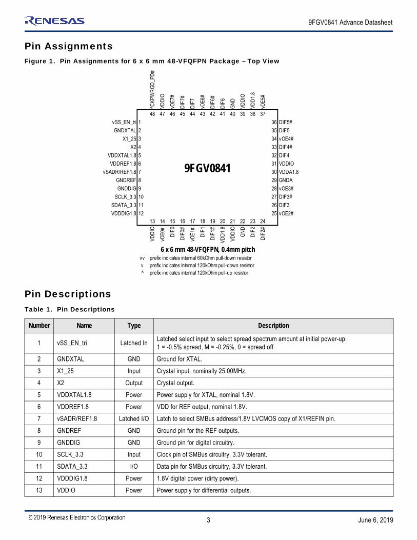
Pin AssignmentsFigure 1. Pin Assignments for 6 x 6 mm 48-VFQFPN Package – Top View
Pin DescriptionsTable 1. Pin Descriptions
Number Name Type Description
1 vSS_EN_tri Latched InLatched select input to select spread spectrum amount at initial power-up:1 = -0.5% spread, M = -0.25%, 0 = spread off
2 GNDXTAL GND Ground for XTAL.
3 X1_25 Input Crystal input, nominally 25.00MHz.
4 X2 Output Crystal output.
5 VDDXTAL1.8 Power Power supply for XTAL, nominal 1.8V.
6 VDDREF1.8 Power VDD for REF output, nominal 1.8V.
7 vSADR/REF1.8 Latched I/O Latch to select SMBus address/1.8V LVCMOS copy of X1/REFIN pin.
8 GNDREF GND Ground pin for the REF outputs.
9 GNDDIG GND Ground pin for digital circuitry.
10 SCLK_3.3 Input Clock pin of SMBus circuitry, 3.3V tolerant.
11 SDATA_3.3 I/O Data pin for SMBus circuitry, 3.3V tolerant.
12 VDDDIG1.8 Power 1.8V digital power (dirty power).
13 VDDIO Power Power supply for differential outputs.
^CKP
WR
GD
_PD
#
VDD
IO
vOE7
#
DIF
7#
DIF
7
vOE6
#
DIF
6#
DIF
6
GN
D
VDD
IO
VDD
1.8
vOE5
#
48 47 46 45 44 43 42 41 40 39 38 37
vSS_EN_tri 1 36 DIF5#
GNDXTAL 2 35 DIF5
X1_25 3 34 vOE4#
X2 4 33 DIF4#
VDDXTAL1.8 5 32 DIF4
VDDREF1.8 6 31 VDDIO
vSADR/REF1.8 7 30 VDDA1.8
GNDREF 8 29 GNDA
GNDDIG 9 28 vOE3#
SCLK_3.3 10 27 DIF3#
SDATA_3.3 11 26 DIF3
VDDDIG1.8 12 25 vOE2#13 14 15 16 17 18 19 20 21 22 23 24
VDD
IO
vOE0
#
DIF
0
DIF
0#
vOE1
#
DIF
1
DIF
1#
VDD
1.8
VDD
IO
GN
D
DIF
2
DIF
2#vv prefix indicates internal 60kOhm pull-down resistorv prefix indicates internal 120kOhm pull-down resistor^ prefix indicates internal 120kOhm pull-up resistor
6 x 6 mm 48-VFQFPN, 0.4mm pitch
9FGV0841

4 June 6, 2019
9FGV0841 Advance Datasheet
14 vOE0# InputActive low input for enabling DIF pair 0. This pin has an internal pull-down.1 =disable outputs, 0 = enable outputs
15 DIF0 Output Differential true clock output.
16 DIF0# Output Differential complementary clock output.
17 vOE1# InputActive low input for enabling DIF pair 1. This pin has an internal pull-down.1 =disable outputs, 0 = enable outputs
18 DIF1 Output Differential true clock output.
19 DIF1# Output Differential complementary clock output.
20 VDD1.8 Power Power supply, nominal 1.8V.
21 VDDIO Power Power supply for differential outputs.
22 GND GND Ground pin.
23 DIF2 Output Differential true clock output.
24 DIF2# Output Differential complementary clock output.
25 vOE2# InputActive low input for enabling DIF pair 2. This pin has an internal pull-down. 1 =disable outputs, 0 = enable outputs
26 DIF3 OUT Differential true clock output.
27 DIF3# OUT Differential complementary clock output.
28 vOE3# InputActive low input for enabling DIF pair 3. This pin has an internal pull-down. 1 =disable outputs, 0 = enable outputs
29 GNDA GND Ground pin for the PLL core.
30 VDDA1.8 Power 1.8V power for the PLL core.
31 VDDIO Power Power supply for differential outputs.
32 DIF4 Output Differential true clock output.
33 DIF4# Output Differential complementary clock output.
34 vOE4# InputActive low input for enabling DIF pair 4. This pin has an internal pull-down. 1 =disable outputs, 0 = enable outputs
35 DIF5 Output Differential true clock output.
36 DIF5# Output Differential complementary clock output.
37 vOE5# InputActive low input for enabling DIF pair 5. This pin has an internal pull-down.1 =disable outputs, 0 = enable outputs
38 VDD1.8 Power Power supply, nominal 1.8V.
39 VDDIO Power Power supply for differential outputs.
40 GND GND Ground pin.
41 DIF6 Output Differential true clock output.
42 DIF6# Output Differential complementary clock output.
43 vOE6# InputActive low input for enabling DIF pair 6. This pin has an internal pull-down. 1 =disable outputs, 0 = enable outputs
44 DIF7 Output Differential true clock output.
Table 1. Pin Descriptions (Cont.)
Number Name Type Description

5 June 6, 2019
9FGV0841 Advance Datasheet
Power Management
1 REF is Hi-Z until the 1st assertion of CKPWRGD_PD# high. After this, when CKPWRG_PD# is low, REF is Low.
45 DIF7# Output Differential complementary clock output.
46 vOE7# InputActive low input for enabling DIF pair 7. This pin has an internal pull-down. 1 =disable outputs, 0 = enable outputs
47 VDDIO Power Power supply for differential outputs.
48 ^CKPWRGD_PD# InputInput notifies device to sample latched inputs and start up on first high assertion. Low enters Power Down Mode, subsequent high assertions exit Power Down Mode. This pin has internal pull-up resistor.
Table 2. Power Management
CKPWRGD_PD# SMBus OE bitDIFx
REFOEx# True Output Complementary Output
0 X X Low Low Hi-Z1
1 1 0 Running Running Running
1 0 1 Low Low Low
Table 3. SMBus Address Selection
SADR Address + Read/Write Bit
State of SADR on first application of CKPWRGD_PD#0 1101000 X
1 1101010 X
Table 4. Power Connections
Pin NumberDescription
VDD VDDIO GND
5 2 XTAL OSC
6 8 REF Power
12 9 Digital (dirty) Power
20, 38 13, 21, 31, 39, 47 22, 29, 40 DIF Outputs
30 29 PLL Analog
Table 1. Pin Descriptions (Cont.)
Number Name Type Description

6 June 6, 2019
9FGV0841 Advance Datasheet
Absolute Maximum RatingsThe absolute maximum ratings are stress ratings only. Stresses greater than those listed below can cause permanent damage to the device. Functional operation of the 9FGV0841 at absolute maximum ratings is not implied. Exposure to absolute maximum rating conditions may affect device reliability.
1 Guaranteed by design and characterization, not 100% tested in production.2 Operation under these conditions is neither implied nor guaranteed.3 Not to exceed 2.5V.
Thermal Characteristics
1 EPAD soldered to board.
Electrical CharacteristicsTA = TAMB; supply voltages per normal operation conditions. See ITest Loads for loading conditions
Table 5. Absolute Maximum Ratings
Parameter Symbol Conditions Minimum Typical Maximum Units Notes
Supply Voltage VDDxx Applies to all VDD pins. -0.5 2.5 V 1,2
Input Voltage VIN -0.5 VDD + 0.5V V 1,3
Input High Voltage, SMBus VIHSMB SMBus clock and data pins. 3.6V V 1
Storage Temperature Ts -65 150 °C 1
Junction Temperature Tj 125 °C 1
Input ESD protection ESD prot Human Body Model. 2000 V 1
Table 6. Thermal Characteristics
Parameter Symbol Conditions Package Typical Values Units Notes
Thermal Resistance
θJC Junction to case.
NDG48
33 °C/W 1
θJb Junction to base. 2.1 °C/W 1
θJA0 Junction to air, still air. 37 °C/W 1
θJA1 Junction to air, 1 m/s air flow. 30 °C/W 1
θJA3 Junction to air, 3 m/s air flow. 27 °C/W 1
θJA5 Junction to air, 5 m/s air flow. 26 °C/W 1
Table 7. Common Electrical Characteristics
Parameter Symbol Conditions Minimum Typical Maximum Units Notes
Supply Voltage VDDxxSupply voltage for core, analog and single-ended LVCMOS outputs.
1.7 1.8 1.9 V
Output Supply Voltage VDDIOSupply voltage for differential Low Power outputs.
0.9975 1.05–1.8 1.9 V
Ambient Operating Temperature
TAMBCommercial range. 0 25 70 °C
Industrial range. -40 25 85 °C

7 June 6, 2019
9FGV0841 Advance Datasheet
1 Guaranteed by design and characterization, not 100% tested in production.2 Control input must be monotonic from 20% to 80% of input swing.3 Time from deassertion until outputs are > 200mV.4 For VDDSMB < 3.3V, VIHSMB > = 0.65 x VDDSMB.
Input High Voltage VIH Single-ended inputs, except SMBus. 0.75 VDD VDD + 0.3 V
Input Mid Voltage VIM Single-ended tri-level inputs ('_tri' suffix). 0.4 VDD 0.5 VDD 0.6 VDD V
Input Low Voltage VIL Single-ended inputs, except SMBus. -0.3 0.25 VDD V
Output High Voltage VOHSingle-ended outputs, except SMBus. IOH = -2mA
VDD-0.45 V
Output Low Voltage VOLSingle-ended outputs, except SMBus. IOL = -2mA
0.45 V
Input Current
IIN Single-ended inputs, VIN = GND, VIN = VDD. -5 5 μA
IINP
Single-ended inputs.
VIN = 0 V; Inputs with internal pull-up resistors.
VIN = VDD; Inputs with internal pull-down resistors.
-20 20 μA
Input Frequency Fin XTAL, or X1 input. 23 25 27 MHz
Pin Inductance Lpin 7 nH 1
CapacitanceCIN Logic Inputs, except DIF_IN. 1.5 5 pF 1
COUT Output pin capacitance. 6 pF 1
Clk Stabilization TSTABFrom VDD Power-Up and after input clock stabilization or de-assertion of PD# to 1st clock.
0.6 1.8 ms 1,2
SS Modulation Frequency fMODAllowable Frequency.
(Triangular Modulation)30 31.6 33 kHz 1
OE# Latency tLATOE#DIF start after OE# assertion.
DIF stop after OE# deassertion1 3 3 clocks 1,3
Tdrive_PD# tDRVPD DIF output enable after PD# de-assertion. 20 300 us 1,3
Tfall tF Fall time of single-ended control inputs. 5 ns 2
Trise tR Rise time of single-ended control inputs. 5 ns 2
SMBus Input Low Voltage VILSMB VDDSMB = 3.3V, see note 4 for VDDSMB < 3.3V. 0.6 V
SMBus Input High Voltage VIHSMB VDDSMB = 3.3V, see note 5 for VDDSMB < 3.3V. 2.1 3.6 V 4
SMBus Output Low Voltage VOLSMB At IPULLUP. 0.4 V
SMBus Sink Current IPULLUP At VOL. 4 mA
Nominal Bus Voltage VDDSMB 1.7 3.6 V
SCLK/SDATA Rise Time tRSMB (Max VIL - 0.15V) to (Min VIH + 0.15V). 1000 ns 1
SCLK/SDATA Fall Time tFSMB (Min VIH + 0.15V) to (Max VIL - 0.15V). 300 ns 1
SMBus Operating Frequency fMAXSMB Maximum SMBus operating frequency. 400 kHz 1
Table 7. Common Electrical Characteristics (Cont.)
Parameter Symbol Conditions Minimum Typical Maximum Units Notes

8 June 6, 2019
9FGV0841 Advance Datasheet
1 Guaranteed by design and characterization, not 100% tested in production.2 Measured from differential waveform.3 Slew rate is measured through the Vswing voltage range centered around differential 0V. This results in a ±150mV window around differential 0V. 4 Matching applies to rising edge rate for Clock and falling edge rate for Clock#. It is measured using a ±75mV window centered on the average
cross point where Clock rising meets Clock# falling. The median cross point is used to calculate the voltage thresholds the oscilloscope is to use for the edge rate calculations
5 VCROSS is defined as voltage where Clock = Clock# measured on a component test board and only applies to the differential rising edge (i.e. Clockrising and Clock# falling).
6 The total variation of all Vcross measurements in any particular system. Note that this is a subset of VCROSS_min/max (VCROSS absolute) allowed.The intent is to limit VCROSS induced modulation by setting Δ-VCROSS to be smaller than VCROSS absolute.
7 At default SMBus amplitude settings.
1 Guaranteed by design and characterization, not 100% tested in production.2 This is the current required to have the REF output running in Wake-on-LAN mode (Byte 3, bit 5 = 1).
Table 8. DIF Low-Power HCSL (LP-HCSL) Outputs
Parameter Symbol Conditions Minimum Typical Maximum Units Notes
Slew Rate TrfScope averaging on fast setting. 1.6 2.3 3.5 V/ns 1,2,3
Scope averaging on slow setting. 1.3 1.9 2.9 V/ns 1,2,3
Slew Rate Matching ΔTrf Slew rate matching, scope averaging on. 7 20 % 1,2,4
Voltage High VHIGH Statistical measurement on single-ended signal using oscilloscope math function (scope averaging on).
660 784 850mV
7
Voltage Low VLOW -150 -33 150 7
Max Voltage Vmax Measurement on single-ended signal using absolute value (scope averaging off).
816 1150mV
7
Min Voltage Vmin -300 -42 7
Vswing Vswing Scope averaging off. 300 1634 mV 1,2,7
Crossing Voltage (abs) Vcross_abs Scope averaging off. 250 427 550 mV 1,5,7
Crossing Voltage (var) Δ-Vcross Scope averaging off. 12 140 mV 1,6,7
Table 9. Current Consumption
Parameter Symbol Conditions Minimum Typical Maximum Units Notes
Operating Supply Current
IDDAOP VDDA, All outputs active at100MHz. 6 9 mA
IDDOPAll VDD, except VDDA and VDDIO, All outputs active at100MHz.
12 16 mA
IDDIOOP VDDIO, All outputs active at100MHz. 28 35 mA
Wake-on-LAN Current
(CKPWRGD_PD# = '0' Byte 3, bit 5 = '1')
IDDAPD VDDA, DIF outputs off, REF output running. 0.4 1 mA 2
IDDPDAll VDD, except VDDA and VDDIO, DIF outputs off, REF output running.
5.3 8 mA 2
IDDIOPD VDDIO, DIF outputs off, REF output running. 0.04 0.1 mA 2
Powerdown Current
(CKPWRGD_PD# = '0'Byte 3, bit 5 = '0')
IDDAPD VDDA, all outputs off. 0.4 1 mA
IDDPDAll VDD, except VDDA and VDDIO, all outputs off.
0.6 1 mA
IDDIOPD VDDIO, all outputs off. 0.0005 0.1 mA

9 June 6, 2019
9FGV0841 Advance Datasheet
1 Guaranteed by design and characterization, not 100% tested in production.2 Measured from differential waveform.
Table 10. DIF Output Duty Cycle, Jitter, and Skew Characteristics
Parameter Symbol Conditions Minimum Typical Maximum Units Notes
Duty Cycle tDC Measured differentially, PLL Mode. 45 50 55 % 1,2
Skew, Output to Output tsk3 Averaging on, VT = 50%. 43 50 ps 1,2
Jitter, Cycle to Cycle tjcyc-cyc 14 50 ps 1,2
Table 11. Filtered Phase Jitter Parameters – PCIe Common Clocked (CC) Architectures
Parameter Symbol Conditions Minimum Typical MaximumSpecification
Limits Units Notes
Phase Jitter, PLL Mode
tjphPCIeG1-CC PCIe Gen1. 21 25 35 86ps
(p-p)1,2,3
tjphPCIeG2-CC
PCIe Gen2 Low Band10kHz < f < 1.5MHz
(PLL BW of 5–16MHz, 8–16MHz, CDR = 5MHz).
0.9 0.9 1.1 3ps
(rms)1,2
PCIe Gen2 High Band
1.5MHz < f < Nyquist (50MHz)
(PLL BW of 5–16MHz, 8–16MHz, CDR = 5MHz).
1.5 1.6 1.9 3.1ps
(rms)1,2
tjphPCIeG3-CC
PCIe Gen3
(PLL BW of 2–4MHz, 2–5MHz, CDR = 10MHz).
0.3 0.37 0.44 1ps
(rms)1,2
tjphPCIeG4-CC
PCIe Gen4
(PLL BW of 2–4MHz, 2–5MHz, CDR = 10MHz).
0.3 0.37 0.44 0.5ps
(rms)1,2
Table 12. REF
Parameter Symbol Conditions Minimum Typical Maximum Units Notes
Long Accuracy ppm See Tperiod min–max values. 0 ppm 1,2
Clock Period Tperiod 25MHz output. 40 ns 2
Rise/Fall Slew Rate trf1 Byte 3 = 1F, 20% to 80% of VDDREF. 0.6 1 1.6 V/ns 1
Rise/Fall Slew Rate trf1 Byte 3 = 5F, 20% to 80% of VDDREF. 0.9 1.4 2.2 V/ns 1,3
Rise/Fall Slew Rate trf1 Byte 3 = 9F, 20% to 80% of VDDREF. 1.1 1.7 2.7 V/ns 1
Rise/Fall Slew Rate trf1 Byte 3 = DF, 20% to 80% of VDDREF. 1.1 1.8 2.9 V/ns 1
Duty Cycle dt1X VT = VDD/2 V. 45 49.1 55 % 1,4
Duty Cycle Distortion dtcd VT = VDD/2 V. 0 2 4 % 1,5
Jitter, Cycle to Cycle tjcyc-cyc VT = VDD/2 V. 19.1 250 ps 1,4

10 June 6, 2019
9FGV0841 Advance Datasheet
1 Guaranteed by design and characterization, not 100% tested in production.2 All Long Term Accuracy and Clock Period specifications are guaranteed assuming that REF is trimmed to 25.00MHz.3 Default SMBus value.4 When driven by a crystal.5 When driven by an external oscillator via the X1 pin, X2 should be floating.
Clock Periods
1 Guaranteed by design and characterization, not 100% tested in production.2 All Long Term Accuracy and Clock Period specifications are guaranteed assuming that REF is trimmed to 0ppm.
Noise Floor tjdBc1k 1kHz offset. -129.8 -105 dBc 1,4
Noise Floor tjdBc10k 10kHz offset to Nyquist. -143.6 -115 dBc 1,4
Jitter, Phase tjphREF 12kHz to 5MHz. 0.63 1.5 ps (rms) 1,4
Table 13. Clock Periods - Differential Outputs with Spread Spectrum Disabled
SSC OFFCenter
FrequencyMHz
Measurement Window
Units Notes
1 Clock 1μs 0.1s 0.1s 0.1s 1μs 1 Clock
-c2c jitter AbsPer
Min
-SSCShort-Term
AverageMin
- ppm Long-Term
AverageMin
0 ppm Period
Nominal
+ ppm Long-Term
AverageMax
+SSC Short-Term
AverageMax
+c2c jitter AbsPer
Max
DIF 100.00 9.94900 — 9.99900 10.00000 10.00100 — 10.05100 ns 1,2
Table 14. Clock Periods - Differential Outputs with Spread Spectrum Enabled
SSC ONCenter
FrequencyMHz
Measurement Window
Units Notes
1 Clock 1μs 0.1s 0.1s 0.1s 1μs 1 Clock
-c2c jitter AbsPer
Min
-SSCShort-Term
AverageMin
- ppm Long-Term
AverageMin
0 ppm Period
Nominal
+ ppm Long-Term
AverageMax
+SSC Short-Term
AverageMax
+c2c jitter AbsPer
Max
DIF 99.75 9.94906 9.99906 10.02406 10.02506 10.02607 10.05107 10.10107 ns 1,2
Table 12. REF (Cont.)
Parameter Symbol Conditions Minimum Typical Maximum Units Notes

11 June 6, 2019
9FGV0841 Advance Datasheet
Crystal Characteristics
ITest LoadsFigure 2. Low-Power HCSL (LP-HCSL) Differential Output Test Load
Figure 3. REF Output Test Load
Table 15. Recommended Crystal Characteristics
Parameter Value Units
Frequency 25 MHz
Resonance Mode Fundamental –
Frequency Tolerance at 25°C ±20 ppm maximum
Frequency Stability, REF at 25°C Over Operating Temperature Range ±20 ppm maximum
Temperature Range (commercial) 0–70 °C
Temperature Range (industrial) -40–85 °C
Equivalent Series Resistance (ESR) 50 Ω maximum
Shunt Capacitance (CO) 7 pF maximum
Load Capacitance (CL) 8 pF maximum
Drive Level 0.1 mW maximum
Aging Per Year ±5 ppm maximum
Rs
Rs2pF 2pF
5 inches
Zo = 100ohm
Device
REF Output
335pF
Zo = 50 ohms

12 June 6, 2019
9FGV0841 Advance Datasheet
Alternate Terminations
Figure 4. Driving LVDS
Table 16. Driving LVDS Inputs
ComponentValue
Receiver has termination Receiver does not have termination
R7a, R7b 10kΩ 140Ω
R8a, R8b 5.6kΩ 75Ω
Cc 0.1uF 0.1uF
Vcm 1.2 Volts 1.2 Volts
Rs
Device
Rs
Zo
Driving LVDS
Cc
Cc R7a R7b
R8a R8b
3.3V
LVDS Clock input

13 June 6, 2019
9FGV0841 Advance Datasheet
General SMBus Serial Interface InformationHow to Write Controller (host) sends a start bit
Controller (host) sends the write address
IDT clock will acknowledge
Controller (host) sends the beginning byte location = N
IDT clock will acknowledge
Controller (host) sends the byte count = X
IDT clock will acknowledge
Controller (host) starts sending Byte N through Byte N+X-1
IDT clock will acknowledge each byte one at a time
Controller (host) sends a stop bit
Note: SMBus address is latched on SADR pin.
How to Read Controller (host) will send a start bit
Controller (host) sends the write address
IDT clock will acknowledge
Controller (host) sends the beginning byte location = N
IDT clock will acknowledge
Controller (host) will send a separate start bit
Controller (host) sends the read address
IDT clock will acknowledge
IDT clock will send the data byte count = X
IDT clock sends Byte N+X-1
IDT clock sends Byte 0 through Byte X (if X(H) was written toByte 8)
Controller (host) will need to acknowledge each byte
Controller (host) will send a not acknowledge bit
Controller (host) will send a stop bit
Index Block Write Operation
Controller (Host) IDT (Slave/Receiver)
T starT bitSlave Address
WR WRiteACK
Beginning Byte = NACK
Data Byte Count = XACK
Beginning Byte N
X ByteACK
OO OO O
OByte N + X - 1
ACKP stoP bit
Index Block Read Operation
Controller (Host) IDT (Slave/Receiver)
T starT bitSlave Address
WR WRiteACK
Beginning Byte = NACK
RT Repeat starTSlave Address
RD ReaD
ACK
Data Byte Count=XACK
X By
te
Beginning Byte NACK
OO OO OO
Byte N + X - 1N Not acknowledgeP stoP bit

14 June 6, 2019
9FGV0841 Advance Datasheet
SMBus Table: Output Enable Register1
1 A low on these bits will override the OE# pin and force the differential output Low/Low.
SMBus Table: SS Readback and Control Register
1 B1[5] must be set to a 1 for these bits to have any effect on the part.
SMBus Table: DIF Slew Rate Control Register
Byte 0 Name Control Function Type 0 1 Default
Bit 7 DIF OE7 Output Enable RW Low/Low Enabled 1
Bit 6 DIF OE6 Output Enable RW Low/Low Enabled 1
Bit 5 DIF OE5 Output Enable RW Low/Low Enabled 1
Bit 4 DIF OE4 Output Enable RW Low/Low Enabled 1
Bit 3 DIF OE3 Output Enable RW Low/Low Enabled 1
Bit 2 DIF OE2 Output Enable RW Low/Low Enabled 1
Bit 1 DIF OE1 Output Enable RW Low/Low Enabled 1
Bit 0 DIF OE0 Output Enable RW Low/Low Enabled 1
Byte 1 Name Control Function Type 0 1 Default
Bit 7 SSENRB1 SS Enable Readback Bit1 R 00' for SS_EN_tri = 0, '01' for SS_EN_tri = 'M', '11 for SS_EN_tri = '1'
Latch
Bit 6 SSENRB1 SS Enable Readback Bit0 R Latch
Bit 5 SSEN_SWCNTRL Enable SW control of SS RWValues in B1[7:6]
control SS amountValues in B1[4:3]
control SS amount.0
Bit 4 SSENSW1 SS Enable Software Ctl Bit1 RW1 00' = SS Off, '01' = -0.25% SS,
'10' = Reserved, '11'= -0.5% SS
0
Bit 3 SSENSW0 SS Enable Software Ctl Bit0 RW1 0
Bit 2 Reserved 1
Bit 1 AMPLITUDE 1Controls Output Amplitude
RW 00 = 0.6V 01 = 0.7V 1
Bit 0 AMPLITUDE 0 RW 10= 0.8V 11 = 0.9V 0
Byte 2 Name Control Function Type 0 1 Default
Bit 7 SLEWRATESEL DIF7 Adjust Slew Rate of DIF7 RW Slow Setting Fast Setting 1
Bit 6 SLEWRATESEL DIF6 Adjust Slew Rate of DIF6 RW Slow Setting Fast Setting 1
Bit 5 SLEWRATESEL DIF5 Adjust Slew Rate of DIF5 RW Slow Setting Fast Setting 1
Bit 4 SLEWRATESEL DIF4 Adjust Slew Rate of DIF4 RW Slow Setting Fast Setting 1
Bit 3 SLEWRATESEL DIF3 Adjust Slew Rate of DIF3 RW Slow Setting Fast Setting 1
Bit 2 SLEWRATESEL DIF2 Adjust Slew Rate of DIF2 RW Slow Setting Fast Setting 1
Bit 1 SLEWRATESEL DIF1 Adjust Slew Rate of DIF1 RW Slow Setting Fast Setting 1
Bit 0 SLEWRATESEL DIF0 Adjust Slew Rate of DIF0 RW Slow Setting Fast Setting 1

15 June 6, 2019
9FGV0841 Advance Datasheet
SMBus Table: Nominal VHIGH Amplitude Control / REF Control Register
Byte 4 is Reserved.
SMBus Table: Revision and Vendor ID Register
SMBus Table: Device Type/Device ID Register
Byte 3 Name Control Function Type 0 1 Default
Bit 7REF Slew Rate Control
RW 00 = Slowest 01 = Slow 0
Bit 6 RW 10 = Fast 11 = Faster 1
Bit 5REF Power
Down FunctionWake-on-Lan Enable for REF RW REF does not run in Power Down REF runs in Power Down 0
Bit 4 REF OE REF Output Enable RW Low Enabled 1
Bit 3 Reserved 1
Bit 2 Reserved 1
Bit 1 Reserved 1
Bit 0 Reserved 1
Byte 5 Name Control Function Type 0 1 Default
Bit 7 RID3
Revision ID
R
Industrial: 0001 (revision A)
Automotive; 1000 (revision A)
0
Bit 6 RID2 R 0
Bit 5 RID1 R 0
Bit 4 RID0 R 1
Bit 3 VID3
VENDOR ID
R
0001 = IDT
0
Bit 2 VID2 R 0
Bit 1 VID1 R 0
Bit 0 VID0 R 1
Byte 6 Name Control Function Type 0 1 Default
Bit 7 Device Type1Device Type
R 00 = FGx, 01 = DBx ZDB/FOB,
10 = DMx, 11= DBx FOB
0
Bit 6 Device Type0 R 0
Bit 5 Device ID5
Device ID
R
001000 binary or 08 hex
0
Bit 4 Device ID4 R 0
Bit 3 Device ID3 R 1
Bit 2 Device ID2 R 0
Bit 1 Device ID1 R 0
Bit 0 Device ID0 R 0
16 June 6, 2019
9FGV0841 Advance Datasheet
SMBus Table: Revision and Vendor ID Register
Package Outline DrawingsThe package outline drawings are appended at the end of this document and are also accessible from the link below. The package information is the most current data available and is subject to change without notice or revision of this document.
Commercial and Industrial Deviceswww.idt.com/document/psc/48-vfqfpn-package-outline-drawing-60-x-60-x-090-mm-body-epad-42-x-42-mm-040mm-pitch-ndg48p2
Automotive Deviceswww.idt.com/document/psc/48-vfqfpn-package-outline-drawing-48-vfqfpn-package-outline-drawing-ndg48s1-wettable-flank
Marking Diagrams
Byte 7 Name Control Function Type 0 1 Default
Bit 7 Reserved 0
Bit 6 Reserved 0
Bit 5 Reserved 0
Bit 4 BC4
Byte Count Programming
RW
Writing to this register will configure how many bytes will be read back,
default is = 8 bytes.
0
Bit 3 BC3 RW 1
Bit 2 BC2 RW 0
Bit 1 BC1 RW 0
Bit 0 BC0 RW 0
Lines 1 and 2: truncated part number
“YYWW” denotes the last digits of the year and work week the part was assembled.
“#” denotes the stepping sequence.
“$” denotes mark code.
“COO” denotes country of origin/
“LOT” denotes the lot number.
Commercial Industrial Automotive

DISCLAIMER Integrated Device Technology, Inc. (IDT) and its affiliated companies (herein referred to as “IDT”) reserve the right to modify the products and/or specifications described herein at any time,without notice, at IDT’s sole discretion. Performance specifications and operating parameters of the described products are determined in an independent state and are not guaranteed to perform the sameway when installed in customer products. The information contained herein is provided without representation or warranty of any kind, whether express or implied, including, but not limited to, the suitabilityof IDT's products for any particular purpose, an implied warranty of merchantability, or non-infringement of the intellectual property rights of others. This document is presented only as a guide and does notconvey any license under intellectual property rights of IDT or any third parties.
IDT's products are not intended for use in applications involving extreme environmental conditions or in life support systems or similar devices where the failure or malfunction of an IDT product can be rea-sonably expected to significantly affect the health or safety of users. Anyone using an IDT product in such a manner does so at their own risk, absent an express, written agreement by IDT.
Integrated Device Technology, IDT and the IDT logo are trademarks or registered trademarks of IDT and its subsidiaries in the United States and other countries. Other trademarks used herein are the propertyof IDT or their respective third party owners. For datasheet type definitions and a glossary of common terms, visit www.idt.com/go/glossary. Integrated Device Technology, Inc. All rights reserved.
Tech Supportwww.IDT.com/go/support
Sales1-800-345-7015 or 408-284-8200Fax: 408-284-2775www.IDT.com/go/sales
Corporate Headquarters6024 Silver Creek Valley Road San Jose, CA 95138 USAwww.IDT.com
17©2019 Integrated Device Technology, Inc. June 6, 2019
9FGV0841 Advance Datasheet
Ordering Information
“LF” indicates Pb-free, RoHS compliant.
“A” is the device revision designator (will not correlate to with the datasheet revision).
Revision History
Orderable Part Number Package Carrier Type Temperature
9FGV0841AKLF 6 × 6 mm, 0.4mm pitch 48-VFQFPN Tray 0 to +70°C
9FGV0841AKLFT 6 × 6 mm, 0.4mm pitch 48-VFQFPN Reel 0 to +70°C
9FGV0841AKILF 6 × 6 mm, 0.4mm pitch 48-VFQFPN Tray -40 to +85°C
9FGV0841AKILFT 6 × 6 mm, 0.4mm pitch 48-VFQFPN Reel -40 to +85°C
9FGV0841ANDG2 6 × 6 mm, 0.4mm pitch 48-VFQFPN (wettable flank) Tray -40 to +105°C
9FGV0841ANDG28 6 × 6 mm, 0.4mm pitch 48-VFQFPN (wettable flank) Reel -40 to +105°C
Revision Date Description of Change
June 6, 2019 Changed Input Current minimum and maximum values from -200/200µA to -20/20µA.
May 16, 2019 Added automotive information.
January 24, 2018 Corrected Byte 5 bit 4 to be '1' instead of '0'.
June 26, 2017 Updated front page general description to reflect the PCIe Gen4 updates. Updated Electrical Characteristics - Filtered Phase Jitter Parameters - PCIe Common Clocked (CC)
Architectures table and added PCIe Gen4 Data.
October 18, 2016 Removed IDT crystal part number.
November 12, 2015 Updated Package outline drawings.

48-VFQFPN Package Outline Drawing
6.0 x 6.0 x 0.90 mm Body, Epad 4.2 x 4.2 mm, 0.40mm PitchNDG48P2, PSC-4212-02, Rev 03, Page 1
© Renesas Electronics Corporation

48-VFQFPN Package Outline Drawing
6.0 x 6.0 x 0.90 mm Body, Epad 4.2 x 4.2 mm, 0.40mm PitchNDG48P2, PSC-4212-02, Rev 03, Page 2
Package Revision HistoryRev No.Date Created Description
Feb 25, 2020 Rev 03 Tolerance Format Change
July 24, 2018 Rev 02 New Format Change QFN to VFQFPN, Recalculate Land Pattern
© Renesas Electronics Corporation

© Integrated Device Technology, Inc.
48-VFQFPN, Package Outline Drawing
6.00 x 6.00 x 0.90 mm Body, 0.4mm PitchNDG48S1 Wettable Flank, PSC-4212-04, Rev 00, Page 1

© Integrated Device Technology, Inc.
48-VFQFPN, Package Outline Drawing
6.00 x 6.00 x 0.90 mm Body, 0.4mm PitchNDG48S1 Wettable Flank, PSC-4212-04, Rev 00, Page 2
Package Revision HistoryRev No.Date Created Description
May 3, 2019 Rev 00 Initial Release

20
Corporate HeadquartersTOYOSU FORESIA, 3-2-24 Toyosu,Koto-ku, Tokyo 135-0061, Japanwww.renesas.com
Contact InformationFor further information on a product, technology, the most up-to-date version of a document, or your nearest sales office, please visit:www.renesas.com/contact/
TrademarksRenesas and the Renesas logo are trademarks of Renesas Electronics Corporation. All trademarks and registered trademarks are the property of their respective owners.