8-bit flash microcontroller with 64k bytes program memory - keil
TRANSCRIPT

8-bit Flash Microcontroller with 64K bytes Program Memory
AT89LP51RD2AT89LP51ED2AT89LP51ID2Preliminary
3714A–MICRO–7/11
Features• 8-bit Microcontroller Compatible with 8051 Products• Enhanced 8051 Architecture
– Single Clock Cycle per Byte Fetch– 12 Clock per Machine Cycle Compatibility Mode– Up to 20 MIPS Throughput at 20 MHz Clock Frequency– Fully Static Operation: 0 Hz to 20 MHz– On-chip 2-cycle Hardware Multiplier– 16x16 Multiply–Accumulate Unit– 256 x 8 Internal RAM– On-chip 2KB Expanded RAM (ERAM)
• Software Selectable Size (0, 256, 512, 768, 1024, 1792, 2048 Bytes)– Dual Data Pointers– 4-level Interrupt Priority
• Nonvolatile Program and Data Memory– 64KB of In-System Programmable (ISP) Flash Program Memory– 4KB of EEPROM (AT89LP51ED2/ID2 Only)– 512-byte User Signature Array– Endurance: 10,000 Write/Erase Cycles– Serial Interface for Program Downloading– 2KB Boot ROM Contains Low Level Flash Programming Routines and a Default
Serial Bootloader• Peripheral Features
– Three 16-bit Enhanced Timer/Counters– Seven 8-bit PWM Outputs– 16-bit Programmable Counter Array
• High Speed Output, Compare/Capture• Pulse Width Modulation, Watchdog Timer Capabilities
– Enhanced UART with Automatic Address Recognition and Framing Error Detection
– Enhanced Master/Slave SPI with Double-buffered Send/Receive– Two Wire Interface 400K bit/s– Programmable Watchdog Timer with Software Reset– 8 General-purpose Interrupt and Keyboard Interface Pins
• Special Microcontroller Features– Dual Oscillator Support: Crystal, 32 kHz Crystal, 8 MHz Internal (AT89LP51ID2)– Two-wire On-Chip Debug Interface– Brown-out Detection and Power-on Reset with Power-off Flag– Selectable Polarity External Reset Pin– Low Power Idle and Power-down Modes– Interrupt Recovery from Power-down Mode– 8-bit Clock Prescaler
• I/O and Packages– Up to 40 Programmable I/O Lines– Green (Pb/Halide-free) PLCC44, VQFP44, QFN44. PDIP40– Configurable I/O Modes
• Quasi-bidirectional (80C51 Style), Input-only (Tristate)• Push-pull CMOS Output, Open-drain
• Operating Conditions– 2.4V to 5.5V VCC Voltage Range– -40° C to 85°C Temperature Range– 0 to 20 MHz @ 2.4V–5.5V (Single-cycle)

1. Pin Configurations
1.1 44-lead TQFP/LQFP
1.2 44-lead PLCC
1 2 3 4 5 6 7 8 9 10 11
33 32 31 30 29 28 27 26 25 24 23
44
43
42
41
40
39
38
37
36
35
34
12
13
14
15
16
17
18
19
20
21
22
(†MOSI/CEX2/MISO) P1.5(†MISO/CEX3/SCK) P1.6(†SCK/CEX4/MOSI) P1.7
(DCL) RST(RXD) P3.0(SDA) P4.1(TXD) P3.1(INT0) P3.2(INT1) P3.3
(T0) P3.4(T1) P3.5
P0.4 (AD4)P0.5 (AD5)P0.6 (AD6)P0.7 (AD7)POLP4.0 (SCL)P4.4 (ALE)P4.5 (PSEN)P2.7 (A15/AIN3)P2.6 (A14/AIN2)P2.5 (A13/AIN1)
P1.
4 (C
EX
1/S
S†)
P1.
3 (C
EX
0)P
1.2
(EC
I)P
1.1
(T2
EX
/SS
)P
1.0
(T2/
XTA
L1B
‡)P
4.2
(XTA
L2B
‡)
VC
CP
0.0
(AD
0)P
0.1
(AD
1)P
0.2
(AD
2)P
0.3
(AD
3)
(WR
) P
3.6
(RD
) P
3.7
(XTA
L2A
) P
4.7
(XTA
L1A
) P
4.6
VS
S(D
DA
) P
4.3
(A8)
P2.
0(A
9) P
2.1
(DA
C-/
A10
) P
2.2
(DA
C+
/A11
) P
2.3
(AIN
0/A
12)
P2.
4
† SPI in remap mode‡ AT89LP51ID2 Only
7 8 9 10 11 12 13 14 15 16 17
39 38 37 36 35 34 33 32 31 30 29
(†MOSI/CEX2/MISO) P1.5(†MISO/CEX3/SCK) P1.6(†SCK/CEX4/MOSI) P1.7
(DCL) RST(RXD) P3.0(SDA) P4.1(TXD) P3.1(INT0) P3.2(INT1) P3.3
(T0) P3.4(T1) P3.5
P0.4 (AD4)P0.5 (AD5)P0.6 (AD6)P0.7 (AD7)POLP4.0 (SCL)P4.4 (ALE)P4.5 (PSEN)P2.7 (A15/AIN3)P2.6 (A14/AIN2)P2.5 (A13/AIN1)
6 5 4 3 2 1 44
43
42
41
40
18
19
20
21
22
23
24
25
26
27
28
(WR
) P
3.6
(RD
) P
3.7
(XTA
L2A
) P
4.7
(XTA
L1A
) P
4.6
VS
S(D
DA
) P
4.3
(A8)
P2.
0(A
9) P
2.1
(DA
C-/
A10
) P
2.2
(DA
C+
/A11
) P
2.3
(AIN
0/A
12)
P2.
4
P1.
4 (C
EX
1/S
S†)
P
1.3
(CE
X0)
P1.
2 (E
CI)
P1.
1 (T
2 E
X/S
S)
P1.
0 (T
2/X
TAL1
B‡)
P4.
2 (X
TAL2
B‡)
V
CC
P0.
0 (A
D0)
P0.
1 (A
D1)
P0.
2 (A
D2)
P0.
3 (A
D3)
† SPI in remap mode‡ AT89LP51ID2 Only
23714A–MICRO–7/11
AT89LP51RD2/ED2/ID2 Preliminary

AT89LP51RD2/ED2/ID2 Preliminary
1.3 44-pad VQFN/QFN/MLF
1.4 40-pin PDIP
Note: 1. The AT89LP51ID2 is not available in the PDIP package
1 2 3 4 5 6 7 8 9 10 11
33 32 31 30 29 28 27 26 25 24 23
44
43
42
41
40
39
38
37
36
35
34
12
13
14
15
16
17
18
19
20
21
22
Bottom pad should be soldered to ground
NOTE:
† SPI in remap mode‡ AT89LP51ID2 Only
(†MOSI/CEX2/MISO) P1.5(†MISO/CEX3/SCK) P1.6(†SCK/CEX4/MOSI) P1.7
(DCL) RST(RXD) P3.0(SDA) P4.1(TXD) P3.1(INT0) P3.2(INT1) P3.3
(T0) P3.4(T1) P3.5
P0.4 (AD4)P0.5 (AD5)P0.6 (AD6)P0.7 (AD7)POLP4.0 (SCL)P4.4 (ALE)P4.5 (PSEN)P2.7 (A15/AIN3)P2.6 (A14/AIN2)P2.5 (A13/AIN1)
P1.
4 (C
EX
1/S
S†)
P1.
3 (C
EX
0)P
1.2
(EC
I)P
1.1
(T2
EX
/SS
)P
1.0
(T2/
XTA
L1B
‡)P
4.2
(XTA
L2B
‡)V
DD
P0.
0 (A
D0)
P0.
1 (A
D1)
P0.
2 (A
D2)
P0.
3 (A
D3)
(WR
) P
3.6
(RD
) P
3.7
(XTA
L2A
) P
4.7
(XTA
L1A
) P
4.6
GN
D(D
DA
) P
4.3
(A8)
P2.
0(A
9) P
2.1
(DA
-/A
10)
P2.
2(D
A+
/A11
) P
2.3
(AIN
0/A
12)
P2.
4
1 2 3 4 5 6 7 8 9 10 11 12 13 14 15 16 17 18 19 20
40 39 38 37 36 35 34 33 32 31 30 29 28 27 26 25 24 23 22 21
(T2) P1.0(SS/T2EX) P1.1
(ECI) P1.2(CEX0) P1.3
(†SS/CEX1) P1.4(†MOSI/CEX2/MISO) P1.5
(†MISO/CEX3/SCL) P1.6(†SCK/CEX4/MOSI) P1.7
RST(RXD) P3.0(TXD) P3.1(INT0) P3.2(INT1) P3.3
(T0) P3.4(T1) P3.5
(WR) P3.6(RD) P3.7
(XTAL2A) P4.7(XTAL1A) P4.6
GND
VDDP0.0 (AD0)P0.1 (AD1)P0.2 (AD2)P0.3 (AD3)P0.4 (AD4)P0.5 (AD5)P0.6 (AD6)P0.7 (AD7)POLP4.4 (ALE)P4.5 (PSEN)P2.7 (A15/AIN3)P2.6 (A14/AIN2)P2.5 (A13/AIN1)P2.4 (A12/AIN0)P2.3 (A11/DAC+)P2.2 (A10/DAC-)P2.1 (A9)P2.0 (A8)
†SPI in remap mode
33714A–MICRO–7/11
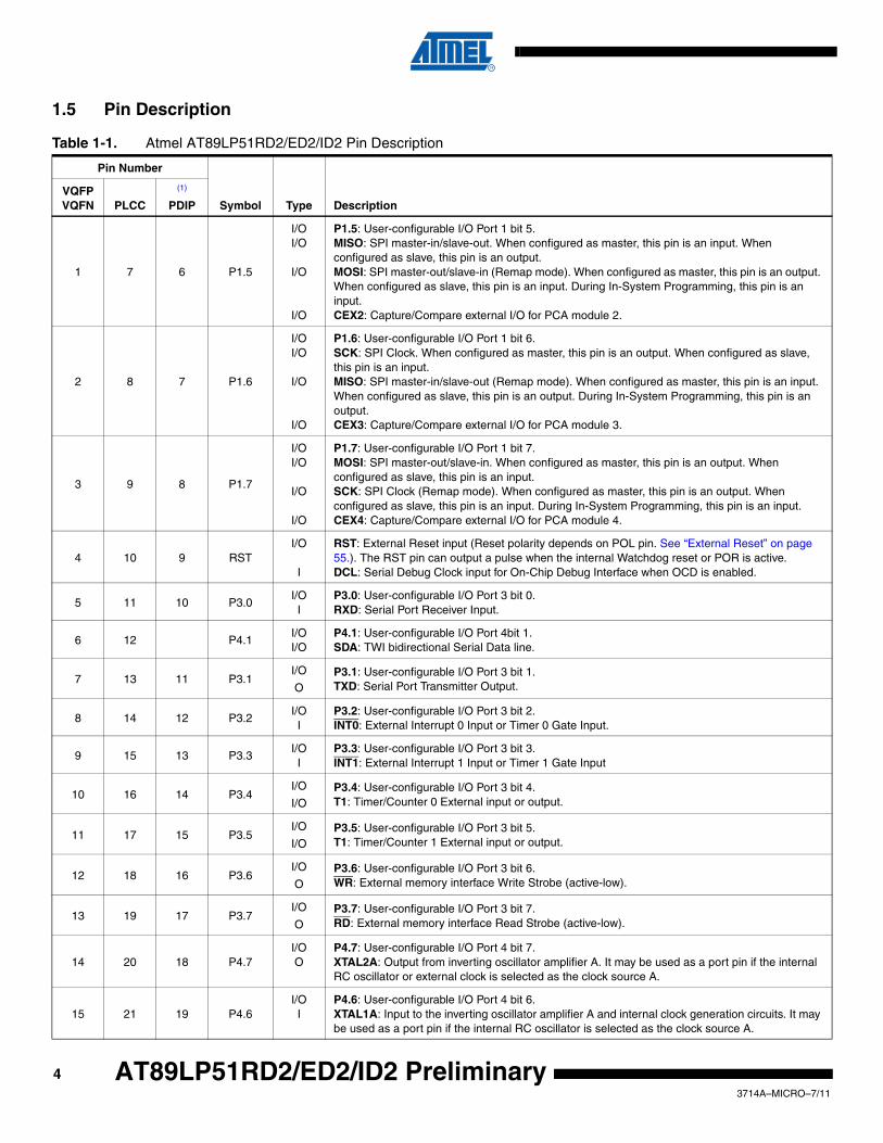
1.5 Pin Description
Table 1-1. Atmel AT89LP51RD2/ED2/ID2 Pin Description
Pin Number
Symbol Type DescriptionVQFPVQFN PLCC
(1)
PDIP
1 7 6 P1.5
I/OI/O
I/O
I/O
P1.5: User-configurable I/O Port 1 bit 5.MISO: SPI master-in/slave-out. When configured as master, this pin is an input. When configured as slave, this pin is an output.MOSI: SPI master-out/slave-in (Remap mode). When configured as master, this pin is an output. When configured as slave, this pin is an input. During In-System Programming, this pin is an input.CEX2: Capture/Compare external I/O for PCA module 2.
2 8 7 P1.6
I/OI/O
I/O
I/O
P1.6: User-configurable I/O Port 1 bit 6.SCK: SPI Clock. When configured as master, this pin is an output. When configured as slave, this pin is an input.MISO: SPI master-in/slave-out (Remap mode). When configured as master, this pin is an input. When configured as slave, this pin is an output. During In-System Programming, this pin is an output.CEX3: Capture/Compare external I/O for PCA module 3.
3 9 8 P1.7
I/OI/O
I/O
I/O
P1.7: User-configurable I/O Port 1 bit 7.MOSI: SPI master-out/slave-in. When configured as master, this pin is an output. When configured as slave, this pin is an input.SCK: SPI Clock (Remap mode). When configured as master, this pin is an output. When configured as slave, this pin is an input. During In-System Programming, this pin is an input.CEX4: Capture/Compare external I/O for PCA module 4.
4 10 9 RSTI/O
I
RST: External Reset input (Reset polarity depends on POL pin. See “External Reset” on page 55.). The RST pin can output a pulse when the internal Watchdog reset or POR is active.DCL: Serial Debug Clock input for On-Chip Debug Interface when OCD is enabled.
5 11 10 P3.0I/OI
P3.0: User-configurable I/O Port 3 bit 0.RXD: Serial Port Receiver Input.
6 12 P4.1I/OI/O
P4.1: User-configurable I/O Port 4bit 1.SDA: TWI bidirectional Serial Data line.
7 13 11 P3.1I/O
OP3.1: User-configurable I/O Port 3 bit 1.TXD: Serial Port Transmitter Output.
8 14 12 P3.2I/OI
P3.2: User-configurable I/O Port 3 bit 2.INT0: External Interrupt 0 Input or Timer 0 Gate Input.
9 15 13 P3.3I/OI
P3.3: User-configurable I/O Port 3 bit 3.INT1: External Interrupt 1 Input or Timer 1 Gate Input
10 16 14 P3.4I/O
I/OP3.4: User-configurable I/O Port 3 bit 4.T1: Timer/Counter 0 External input or output.
11 17 15 P3.5I/O
I/OP3.5: User-configurable I/O Port 3 bit 5.T1: Timer/Counter 1 External input or output.
12 18 16 P3.6I/O
OP3.6: User-configurable I/O Port 3 bit 6.WR: External memory interface Write Strobe (active-low).
13 19 17 P3.7I/O
OP3.7: User-configurable I/O Port 3 bit 7.RD: External memory interface Read Strobe (active-low).
14 20 18 P4.7I/OO
P4.7: User-configurable I/O Port 4 bit 7.XTAL2A: Output from inverting oscillator amplifier A. It may be used as a port pin if the internal RC oscillator or external clock is selected as the clock source A.
15 21 19 P4.6I/OI
P4.6: User-configurable I/O Port 4 bit 6.XTAL1A: Input to the inverting oscillator amplifier A and internal clock generation circuits. It may be used as a port pin if the internal RC oscillator is selected as the clock source A.
43714A–MICRO–7/11
AT89LP51RD2/ED2/ID2 Preliminary
AT89LP51RD2/ED2/ID2 Preliminary
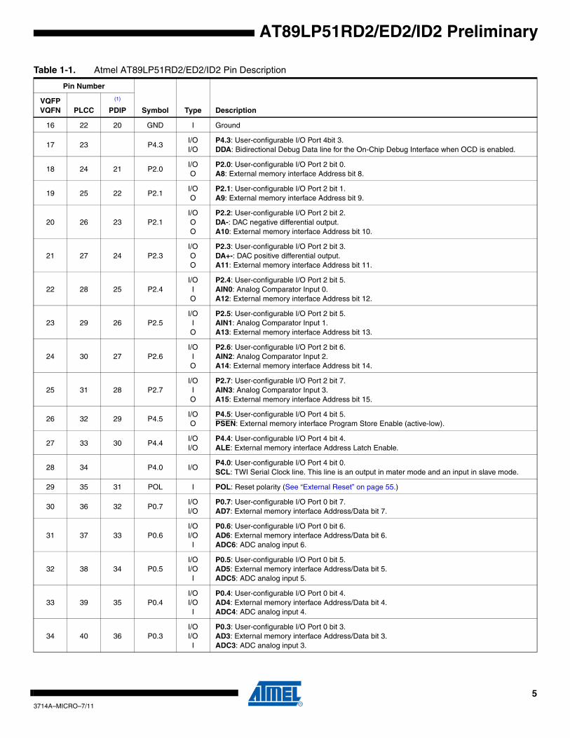
16 22 20 GND I Ground
17 23 P4.3I/OI/O
P4.3: User-configurable I/O Port 4bit 3.DDA: Bidirectional Debug Data line for the On-Chip Debug Interface when OCD is enabled.
18 24 21 P2.0I/OO
P2.0: User-configurable I/O Port 2 bit 0.A8: External memory interface Address bit 8.
19 25 22 P2.1I/OO
P2.1: User-configurable I/O Port 2 bit 1.A9: External memory interface Address bit 9.
20 26 23 P2.1I/OOO
P2.2: User-configurable I/O Port 2 bit 2.DA-: DAC negative differential output.A10: External memory interface Address bit 10.
21 27 24 P2.3I/OOO
P2.3: User-configurable I/O Port 2 bit 3.DA+-: DAC positive differential output.A11: External memory interface Address bit 11.
22 28 25 P2.4I/OIO
P2.4: User-configurable I/O Port 2 bit 5.AIN0: Analog Comparator Input 0.A12: External memory interface Address bit 12.
23 29 26 P2.5I/OIO
P2.5: User-configurable I/O Port 2 bit 5.AIN1: Analog Comparator Input 1.A13: External memory interface Address bit 13.
24 30 27 P2.6I/OIO
P2.6: User-configurable I/O Port 2 bit 6.AIN2: Analog Comparator Input 2.A14: External memory interface Address bit 14.
25 31 28 P2.7I/OIO
P2.7: User-configurable I/O Port 2 bit 7.AIN3: Analog Comparator Input 3.A15: External memory interface Address bit 15.
26 32 29 P4.5I/OO
P4.5: User-configurable I/O Port 4 bit 5.PSEN: External memory interface Program Store Enable (active-low).
27 33 30 P4.4I/OI/O
P4.4: User-configurable I/O Port 4 bit 4.ALE: External memory interface Address Latch Enable.
28 34 P4.0 I/OP4.0: User-configurable I/O Port 4 bit 0.SCL: TWI Serial Clock line. This line is an output in mater mode and an input in slave mode.
29 35 31 POL I POL: Reset polarity (See “External Reset” on page 55.)
30 36 32 P0.7I/OI/O
P0.7: User-configurable I/O Port 0 bit 7.AD7: External memory interface Address/Data bit 7.
31 37 33 P0.6I/OI/OI
P0.6: User-configurable I/O Port 0 bit 6.AD6: External memory interface Address/Data bit 6.ADC6: ADC analog input 6.
32 38 34 P0.5I/OI/OI
P0.5: User-configurable I/O Port 0 bit 5.AD5: External memory interface Address/Data bit 5.ADC5: ADC analog input 5.
33 39 35 P0.4I/OI/OI
P0.4: User-configurable I/O Port 0 bit 4.AD4: External memory interface Address/Data bit 4.ADC4: ADC analog input 4.
34 40 36 P0.3I/OI/OI
P0.3: User-configurable I/O Port 0 bit 3.AD3: External memory interface Address/Data bit 3.ADC3: ADC analog input 3.
Table 1-1. Atmel AT89LP51RD2/ED2/ID2 Pin Description
Pin Number
Symbol Type DescriptionVQFPVQFN PLCC
(1)
PDIP
53714A–MICRO–7/11

Note: 1. The AT89LP51ID2 is not available in the PDIP package
2. OverviewThe Atmel® AT89LP51RD2/ED2/ID2 is a low-power, high-performance CMOS 8-bit 8051 micro-controller with 64KB of In-System Programmable Flash program memory. The AT89LP51ED2and AT89LP51ID2 provide an additional 4KB of EEPROM for nonvolatile data storage. Thedevices are manufactured using Atmel's high-density nonvolatile memory technology and arecompatible with the industry-standard 80C51 instruction set.
The AT89LP51RD2/ED2/ID2 is built around an enhanced CPU core that can fetch a single bytefrom memory every clock cycle. In the classic 8051 architecture, each fetch requires 6 clockcyc les , f o rc ing ins t ruc t ions to execu t e in 12 , 24 o r 48 c lock cyc les . In theAT89LP51RD2/ED2/ID2 CPU, standard instructions need only one to four clock cycles providingsix to twelve times more throughput than the standard 8051. Seventy percent of instructionsneed only as many clock cycles as they have bytes to execute, and most of the remaininginstructions require only one additional clock. The enhanced CPU core is capable of 20 MIPSthroughput whereas the classic 8051 CPU can deliver only 4 MIPS at the same current con-sumption. Conversely, at the same throughput as the classic 8051, the new CPU core runs at amuch lower speed and thereby great ly reducing power consumption and EMI. The
35 41 37 P0.2I/OI/OI
P0.2: User-configurable I/O Port 0 bit 2.AD2: External memory interface Address/Data bit 2.ADC2: ADC analog input 2.
36 42 38 P0.1I/OI/OI
P0.1: User-configurable I/O Port 0 bit 1.AD1: External memory interface Address/Data bit 1.ADC1: ADC analog input 1.
37 43 39 P0.0I/OI/OI
P0.0: User-configurable I/O Port 0 bit 0.AD0: External memory interface Address/Data bit 0.ADC0: ADC analog input 0.
38 44 40 VDD I Supply Voltage
39 1 P4.2 I/O
P4.2: User-configurable I/O Port 4bit 2.XTAL2B: Output from low-frequency inverting oscillator amplifier B (AT89LP51ID2 only). It may be used as a port pin if the internal RC oscillator or external clock is selected as the clock source B.
40 2 1 P1.0I/OI/O
P1.0: User-configurable I/O Port 1 bit 0.T2: Timer 2 External Input or Clock Output.XTAL1B: Input to the low-frequency inverting oscillator amplifier B and internal clock generation circuits. It may be used as a port pin if the internal RC oscillator is selected as the clock source B.
41 3 2 P1.1I/OII
P1.1: User-configurable I/O Port 1 bit 1.T2EX: Timer 2 External Capture/Reload Input.SS: SPI Slave-Select.
42 4 3 P1.2 I/O P1.2: User-configurable I/O Port 1 bit 2.
43 5 4 P1.3I/OI/O
P1.3: User-configurable I/O Port 1 bit 3.CEX0: Capture/Compare external I/O for PCA module 0.
44 6 5 P1.4I/OI
I/O
P1.4: User-configurable I/O Port 1 bit 4.SS: SPI Slave-Select (Remap Mode). This pin is an input for In-System ProgrammingCEX1: Capture/Compare external I/O for PCA module 1.
Table 1-1. Atmel AT89LP51RD2/ED2/ID2 Pin Description
Pin Number
Symbol Type DescriptionVQFPVQFN PLCC
(1)
PDIP
63714A–MICRO–7/11
AT89LP51RD2/ED2/ID2 Preliminary

AT89LP51RD2/ED2/ID2 Preliminary
AT89LP51RD2/ED2/ID2 also includes a compatibility mode that will enable classic 12 clock permachine cycle operation for true timing compatibility with the Atmel AT89C51RD2/ED2.
The AT89LP51RD2/ED2/ID2 retains all of the standard features of the AT89C51RD2/ED2,including: 64KB of In-System Programmable Flash program memory, 4KB of EEPROM(AT89LP51ED2/ID2 Only), 256 bytes of RAM, 2KB of expanded RAM, up to 40 I/O lines, three16-bit timer/counters, a Programmable Counter Array, a programmable hardware watchdogtimer, a keyboard interface, a full-duplex enhanced serial port, a serial peripheral interface (SPI),on-chip crystal oscillator, and a four-level, ten-vector interrupt system. A block diagram is shownin Figure 2-1.
In addition, the Atmel® AT89LP51RD2/ED2/ID2 provides a Two-Wire Interface (TWI) for up to400KB/s serial transfer; a 10-bit, 8-channel Analog-to-Digital Converter (ADC) with temperaturesensor and digital-to-analog (DAC) mode; two analog comparators; an 8MHz internal oscillator;and more on-chip data memory than the Atmel AT89C51RD2/ED2 (4KB vs. 2KB EEPROM and2048 vs. 1792 bytes ERAM).
Some standard features on the AT89LP51RD2/ED2/ID2 are enhanced with new modes or oper-ations. Mode 0 of Timer 0 or Timer 1 acts as a variable 9–16 bit timer/counter and Mode 1 actsas a 16-bit auto-reload timer/counter. In addition, each timer/counter may independently drive an8-bit precision pulse width modulation output. Mode 0 (synchronous mode) of the serial portallows flexibility in the phase/polarity relationship between clock and data.
The I/O ports of the AT89LP51RD2/ED2/ID2 can be independently configured in one of fouroperating modes. In quasi-bidirectional mode, the ports operate as in the classic 8051. In input-only mode, the ports are tristated. Push-pull output mode provides full CMOS drivers and open-drain mode provides just a pull-down. Unlike other 8051s, this allows Port 0 to operate with on-chip pull-ups if desired.
The AT89LP51RD2/ED2/ID2 includes an On-Chip Debug (OCD) interface that allows read-mod-ify-write capabilities of the system state and program flow control, and programming of theinternal memories. The on-chip Flash and EEPROM may also be programmed through theUART-based bootloader or the SPI-based In-System programming interface (ISP).
The TWI and OCD features are not available on the PDIP package. The AT89LP51ID2 is alsonot available in the PDIP.
The features of the AT89LP51RD2/ED2/ID2 make it a powerful choice for applications that needpulse width modulation, high speed I/O, and counting capabilities such as alarms, motor control,corded phones, and smart card readers.
73714A–MICRO–7/11

2.1 Block Diagram
Figure 2-1. Atmel AT89LP51RD2/ED2/ID2 Block Diagram
2.2 System ConfigurationThe AT89LP51RD2/ED2/ID2 supports several system configuration options. Nonvolatile optionsare set through user fuses that must be programmed through the flash programming interface.Volatile options are controlled by software through individual bits of special function registers(SFRs). The AT89LP51RD2/ED2/ID2 must be properly configured before correct operation canoccur.
2.2.1 Fuse OptionsTable 2-1 lists the fusible options for the AT89LP51RD2/ED2/ID2. These options maintain theirstate even when the device is powered off. Some may be changed through the Flash API butothers can only be changed with an external device programmer. For more information, seeSection 24.2 “User Configuration Fuses” on page 190.
Flash Code64KB
Port 2Configurable I/O
Port 1Configurable I/O
UART
SPI
Timer 0Timer 1
WatchdogTimer
Crystal orResonator
EEPROM4KB
(AT89LP51ED2/ID2)
Port 4Configurable I/O
Port 3Configurable I/O Timer 2
Port 0Configurable I/O
RAM256 Bytes
XRAMInterface
8051 Single Cycle CPUwith 12-cycle Compatiblity
PORBOD
Dual DataPointers
MultiplyAccumulate
(16 x 16)
ERAM2KB
KeyboardInterface
PCA
Boot ROM2KB
On-ChipDebug
Internal 8 MHzRC Oscillator
ConfigurableOscillator A
10-bitADC/DAC
TWI
7Dual AnalogComparators
Crystal orResonator
ConfigurableOscillator B(AT89LP51ID2)
83714A–MICRO–7/11
AT89LP51RD2/ED2/ID2 Preliminary

AT89LP51RD2/ED2/ID2 Preliminary
2.2.2 Software OptionsTable 2-2 lists some important software configuration bits that affect operation at the systemlevel. These can be changed by the application software but are set to their default values uponany reset. Most peripherals also have multiple configuration bits that are not listed here.
Table 2-1. User Configuration Fuses
Fuse Name Description
Clock Source ASelects between the High Speed Crystal Oscillator, Low Power Crystal Oscillator, External Clock on XTAL1A or Internal RC Oscillator for the source of the system clock when oscillator A is selected.
Clock Source BSelects between the 32 kHzCrystal Oscillator, External Clock on XTAL1B or Internal RC Oscillator for the source of the system clock when oscillator B is selected (AT89LP51ID2 Only).
Oscillator SelectSelects whether oscillator A or B is enabled to boot the device. (AT89LP51ID2 Only)
X2 ModeSelects the default state of whether the clock source is divided by two (X1) or not (X2) to generate the system clock.
Start-up Time Selects time-out delay for the POR/BOD/PWD wake-up period.
Compatibility ModeConfigures the CPU in 12-clock compatibility or single-cycle fast execution mode.
XRAM ConfigurationConfigures if access to on-chip memories that are mapped to the external data memory address space is enabled/disabled by default.
Bootloader Jump Bit Enables or disables the on-ship bootloader.
On-Chip Debug EnableEnables or disables On-Chip Debug. OCD must be enabled prior to using an in-circuit debugger with the device.
In-System Programming Enable Enables or disables In-System Programming.
User Signature Programming Enable Enables or disables programming of User Signature array.
Default Port StateConfigures the default port state as input-only mode (tristated) or quasi-bidirectional mode (weakly pulled high).
Low Power ModeEnables or disables power reduction features for lower system frequencies.
Table 2-2. Important Software Configuration Bits
Bit(s) SFR Location Description
PxM0.yPxM1.y
P0M0, P0M1, P1M0, P1M1, P2M0, P2M1, P3M0, P3M1, P4M0, P4M1
Configures the I/O mode of Port x Pin y to be one of input-only, quasi-bidirectional, push-pull output or open-drain. The default state is controlled by the Default Port State fuse above
CKRL CKRL Selects the division ratio between the oscillator and the system clock
TPS3-0 CLKREG.7-4 Selects the division ratio between the system clock and the timers
ALES AUXR.0 Enables/disables toggling of ALE
EXRAM AUXR.1Enables/disables access to on-chip memories that are mapped to the external data memory address space
WS1-0 AUXR.6-5Selects the number of wait states when accessing external data memory
XSTK AUXR1.4 Configures the hardware stack to be in RAM or extra RAM
EEE EECON.1 Enables/disables access to the on-chip EEPROM
ENBOOT AUXR1.5 Enables/disables access to the on-chip Flash API
93714A–MICRO–7/11

2.3 Comparison to the Atmel AT89C51RD2/ED2/ID2The Atmel® AT89LP51RD2/ED2/ID2 is part of a family of devices with enhanced features thatare fully binary compatible with the 8051 instruction set. The AT89LP51RD2/ED2/ID2 has twomodes of operations, Compatibility mode and Fast mode. In Compatibility mode the instructiontiming, peripheral behavior, SFR addresses, bit assignments and pin functions are identical tothe existing Atmel AT89C51RD2/ED2/ID2 product. Additional enhancements are transparent tothe user and can be used if desired. Fast mode allows greater performance, but with some dif-ferences in behavior. The major enhancements from the AT89C51RD2/ED2/ID2 are outlined inthe following paragraphs and may be useful to users migrating to the AT89LP51RD2/ED2/ID2from older devices. A summary of the differences between Compatibility and Fast modes isg iven in Table 2-3 on page 12. See a lso the Appl ica t ion note “Migra t ing f romAT89C51RD2/ED2/ID2 to AT89LP51RD2/ED2/ID2.”
2.3.1 Instruction ExecutionIn Compatibility mode the Atmel® AT89LP51RD2/ED2/ID2 CPU uses the six-state machinecycle of the standard 8051 where instruction bytes are fetched every three system clock cycles.Execution times in this mode are identical to the Atmel AT89C51RD2/ED2/ID2. For greater per-formance the user can enable Fast mode by disabling the Compatibility fuse. In Fast mode theCPU fetches one code byte from memory every clock cycle instead of every three clock cycles.This greatly increases the throughput of the CPU. Each standard instruction executes in onlyone to four clock cycles. See “Instruction Set Summary” on page 175 for more details. Any soft-ware delay loops or instruction-based timing operations may need to be retuned to achieve thedesired results in Fast mode.
2.3.2 System ClockThe system clock source is not limited to a crystal or external clock. The system clock source isselectable between the crystal oscillator, an externally driven clock and an internal 8.0MHz RCoscillator for AT89LP51RD2/ED2 and clock source A of AT89LP51ID2. Clock source B ofAT89LP51ID2 is not limited to a 32 kHz crystal. The clock source B is selectable between the 32kHz crystal oscillator, an externally driven clock and an internal 8.0MHz RC oscillator. UnlikeAT89C51ID2, the X2 and CKRL features will also affect the OSCB source.
By default in Compatibility mode the system clock frequency is divided by 2 from the externallysupplied XTAL1 frequency for compatibility with standard 8051s (12 clocks per machine cycle).The System Clock Divider can scale the system clock versus the oscillator source (See Section6.8 on page 49). The divide-by-2 can be disabled to operate in X2 mode (6 clocks per machinecycle) or the clock may be further divided to reduce the operating frequency. In Fast mode theclock divider defaults to divide by 1.
2.3.3 ResetThe RST pin of the AT89LP51RD2/ED2/ID2 has selectable polarity using the POL pin (formerlyEA). When POL is high the RST pin is active high with a pull-down resistor and when POL is lowthe RST pin is active low with a pull-up resistor. For existing AT89C51RD2/ED2/ID2 socketswhere EA is tied to VDD, replacing AT89C51RD2/ED2 with AT89LP51RD2/ED2/ID2 will main-tain the active high reset. Note that forcing external execution by tying EA low is not supported.
The AT89LP51RD2/ED2/ID2 includes an on-chip Power-On Reset and Brown-out Detector cir-cuit that ensures that the device is reset from system power up. In most cases a RC startupcircuit is not required on the RST pin, reducing system cost, and the RST pin may be left uncon-nected if a board-level reset is not present.
103714A–MICRO–7/11
AT89LP51RD2/ED2/ID2 Preliminary

AT89LP51RD2/ED2/ID2 Preliminary
2.3.4 Timer/CountersA common prescaler is available to divide the time base for Timer 0, Timer 1, Timer 2 and theWDT. The TPS3-0 bits in the CLKREG SFR control the prescaler (Table 6-8 on page 49). InCompatibility mode TPS3-0 defaults to 0101B, which causes the timers to count once everymachine cycle. The counting rate can be adjusted linearly from the system clock rate to 1/16 ofthe system clock rate by changing TPS3-0. In Fast mode TPS3-0 defaults to 0000B, or the systemclock rate. TPS does not affect Timer 2 in Clock Out or Baud Generator modes.
In Compatibility mode the sampling of the external Timer/Counter pins: T0, T1, T2 and T2EX;and the external interrupt pins, INT0 and INT1, is also controlled by the prescaler. In Fast modethese pins are always sampled at the system clock rate.
Both Timer 0 and Timer 1 can toggle their respective counter pins, T0 and T1, when they over-flow by setting the output enable bits in TCONB.
2.3.5 Interrupt HandlingFast mode allows for faster interrupt response due to the shorter instruction execution times.
2.3.6 Keyboard InterfaceThe AT89LP51RD2/ED2/ID2 does not clear the keyboard flag register (KBF) after a read. Eachbit must be cleared in software. This allows the interrupt to be generate once per flag when mul-tiple flags are set, if desired. To mimic the old behavior the service routine must clear the wholeregister.
The keyboard can also support general edge-triggered interrupts with the addition of theKBMOD register.
2.3.7 Serial PortThe timer prescaler increases the range of achievable baud rates when using Timer 1 to gener-ate the baud rate in UART Modes 1 or 3, including an increase in the maximum baud rateavailable in Compatibility mode. Additional features include automatic address recognition andframing error detection.
The shift register mode (Mode 0) has been enhanced with more control of the polarity, phaseand frequency of the clock and full-duplex operation. This allows emulation of master serialperipheral (SPI) and two-wire (TWI) interfaces.
2.3.8 I/O PortsThe P0, P1, P2 and P3 I/O ports of the AT89LP51RD2/ED2/ID2 may be configured in four differ-ent modes. The default setting depends on the Tristate-Port User Fuse. When the fuse is set allthe I/O ports revert to input-only (tristated) mode at power-up or reset. When the fuse is notactive, ports P1, P2 and P3 start in quasi-bidirectional mode and P0 starts in open-drain mode.P4 always operates in quasi-bidirectional mode. P0 can be configured to have internal pull-upsby placing it in quasi-bidirectional or output modes. This can reduce system cost by removingthe need for external pull-ups on Port 0.
The P4.4–P4.7 pins are additional I/Os that replace the normally dedicated ALE, PSEN, XTAL1and XTAL2 pins of the AT89C51RD2/ED2/ID2. These pins can be used as additional I/Osdepending on the configuration of the clock and external memory.
113714A–MICRO–7/11

2.3.9 SecurityThe AT89LP51RD2/ED2/ID2 does not support the external access pin (EA). Therefore it is notpossible to execute from external program memory in address range 0000H–1FFFH. When thethird Lockbit is enabled (Lock Mode 4) external program execution is disabled for all addressesabove 1FFFH. This differs from AT89C51RD2/ED2/ID2 where Lock Mode 4 prevents EA frombeing sampled low, but may still allow external execution at addresses outside the 8K internalspace.
2.3.10 ProgrammingThe AT89LP51RD2/ED2/ID2 supports a richer command set for In-System Programming (ISP).Ex is t i ng AT89C51RD2/ED2 p rog rammers shou l d be ab le to p rog ram theAT89LP51RD2/ED2/ID2 in byte mode. In page mode the AT89LP51RD2/ED2/ID2 only supportsprogramming of a half-page of 64 bytes and therefore requires an extra address byte as com-pared to AT89C51RD2/ED2. Furthermore the device signature is located at addresses 0000H,0001H and 0003H instead of 0000H, 0100H and 0200H.
Table 2-3. Compatibility Mode versus Fast Mode Summary
Feature Compatibility Fast
Instruction Fetch in System Clocks 3 1
Instruction Execution Time in System Clocks 6, 12, 18 or 24 1, 2, 3, 4 or 5
Default System Clock Divisor 2 1
Default Timer Prescaler Divisor 6 1
Pin Sampling Rate (INT0, INT1, T0, T1, T2, T2EX) Prescaler Rate System Clock
Minimum RST input pulse in System Clocks 12 2
123714A–MICRO–7/11
AT89LP51RD2/ED2/ID2 Preliminary
AT89LP51RD2/ED2/ID2 Preliminary
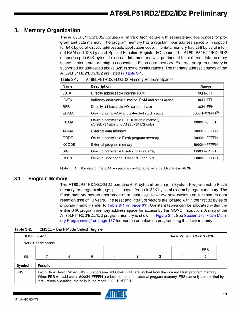
3. Memory OrganizationThe AT89LP51RD2/ED2/ID2 uses a Harvard Architecture with separate address spaces for pro-gram and data memory. The program memory has a regular linear address space with supportfor 64K bytes of directly addressable application code. The data memory has 256 bytes of inter-nal RAM and 128 bytes of Special Function Register I/O space. The AT89LP51RD2/ED2/ID2supports up to 64K bytes of external data memory, with portions of the external data memoryspace implemented on chip as nonvolatile Flash data memory. External program memory issupported for addresses above 32K in some configurations. The memory address spaces of theAT89LP51RD2/ED2/ID2 are listed in Table 3-1.
Note: 1. The size of the EDATA space is configurable with the XRS bits in AUXR.
3.1 Program MemoryThe AT89LP51RD2/ED2/ID2 contains 64K bytes of on-chip In-System Programmable Flashmemory for program storage, plus support for up to 32K bytes of external program memory. TheFlash memory has an endurance of at least 10,000 write/erase cycles and a minimum dataretention time of 10 years. The reset and interrupt vectors are located within the first 83 bytes ofprogram memory (refer to Table 9-1 on page 61). Constant tables can be allocated within theentire 64K program memory address space for access by the MOVC instruction. A map of theAT89LP51RD2/ED2/ID2 program memory is shown in Figure 3-1. See Section 24. “Flash Mem-ory Programming” on page 187 for more information on programming the flash memory.
Table 3-1. AT89LP51RD2/ED2/ID2 Memory Address Spaces
Name Description Range
DATA Directly addressable internal RAM 00H–7FH
IDATA Indirectly addressable internal RAM and stack space 00H–FFH
SFR Directly addressable I/O register space 80H–FFH
EDATA On-chip Extra RAM and extended stack space 0000H–07FFH(1)
FDATAOn-chip nonvolatile EEPROM data memory (AT89LP51ED2 and AT89LP51ID2 only)
0000H–0FFFH
XDATA External data memory 0000H–FFFFH
CODE On-chip nonvolatile Flash program memory 0000H–FFFFH
XCODE External program memory 8000H–FFFFH
SIG On-chip nonvolatile Flash signature array 0000H–01FFH
BOOT On-chip Bootloader ROM and Flash API F800H–FFFFH
Table 3-2. BMSEL – Bank Mode Select Register
BMSEL = 92H Reset Value = XXXX XXX0B
Not Bit Addressable
— — — — — — — FBS
Bit 7 6 5 4 3 2 1 0
Symbol Function
FBS Fetch Bank Select. When FBS = 0 addresses 8000H–FFFFH are fetched from the internal Flash program memory. When FBS = 1 addresses 8000H–FFFFH are fetched from the external program memory. FBS can only be modified by instructions executing internally in the range 0000H–7FFFH.
133714A–MICRO–7/11

Figure 3-1. Program Memory Map
3.1.1 External Program Memory The AT89LP51RD2/ED2/ID2 implements the entire 16-bit, 64 KB program memory space inter-nally. The AT89LP51RD2/ED2/ID2 does not support forcing external execution using the EA pin;however it does include a bank-switching mechanism to allow for up to 32 KB of external pro-gram memory to be mapped into the upper half of the address space. The FBS bit in the BMSELSFR (Table 3-2) selects whether addresses 8000H–FFFFH are mapped to internal or externalprogram memory. FBS can only be modified by instructions executing internally in the range0000H–7FFFH
The AT89LP51RD2/ED2/ID2 uses the standard 8051 external program memory interface withthe upper address on Port 2, the lower address and data in/out multiplexed on Port 0, and theALE and PSEN strobes. Program memory addresses are always 16-bits wide. External programexecution sacrifices two full 8-bit ports, P0 and P2, to the function of addressing the programmemory.
Figure 3-2 shows a hardware configuration for accessing up to 64K bytes of external ROM usinga 16-bit linear address. Port 0 serves as a multiplexed address/data bus to the ROM. TheAddress Latch Enable strobe (ALE) is used to latch the lower address byte into an external reg-ister so that Port 0 can be freed for data input/output. Port 2 provides the upper address bytethroughout the operation. PSEN strobes the external memory.
Figure 3-3 shows the timing of the external program memory interface. ALE is emitted at a con-stant rate of 1/3 of the system clock with a 1/3 duty cycle. PSEN is emitted at a similar rate, butwith 50% duty cycle. The new address changes in the middle of the ALE pulse for latching onthe falling edge and is tristated at the falling edge of PSEN. The instruction data is sampled fromP0 and latched internally during the high phase of the clock prior to the rising edge of PSEN.This timing applies to both Compatibility and Fast modes. In Compatibility mode there is no dif-ference in instruction timing between internal and external execution.
0000
FFFF
0000
007F
User Signature Array
0100
01FF
Atmel Signature Array
SIGEN=0
SIGEN=1
80007FFF
External Program Memory
(XCODE: 30KB)
Internal Program Memory
(CODE: 32KB)
0000
FFFF
0000
007F
User Signature Array
0100
01FF
Atmel Signature Array
Internal Program Memory
(CODE: 62KB)
FBS = 0ENBOOT = 1
F800F7FF
Boot ROM
(BOOT: 2KB)
0000
FFFF
0000
007F
User Signature Array
0100
01FF
Atmel Signature Array
Internal Program Memory
(CODE: 64KB)
FBS = 0ENBOOT = 0
0000
FFFF
0000
007F
User Signature Array
0100
01FF
Atmel Signature Array
80007FFF
External Program Memory
(XCODE: 32KB)
Internal Program Memory
(CODE: 32KB)
FBS = 1ENBOOT = 1
FBS = 1ENBOOT = 0
F800F7FF
Boot ROM
(BOOT: 2KB)
143714A–MICRO–7/11
AT89LP51RD2/ED2/ID2 Preliminary

AT89LP51RD2/ED2/ID2 Preliminary
Figure 3-2. Executing from External Program Memory
Figure 3-3. External Program Memory Fetches
In order for Fast mode to fetch externally, two wait states must be inserted for every clock cycle,increasing the instruction execution time by a factor of 3. However, due to other optimizations,external Fast mode instructions may still be 1/4 to 1/2 faster than their Compatibility mode equiv-alents. Note that if ALE is allowed to toggle in Fast mode, there is a possibility that when theCPU jumps from internal to external execution a short pulse may occur on ALE as shown in Fig-ure 3-4. The setup time from the address to the falling edge of ALE remains the same. However,this behavior can be avoided by setting the DISALE bit prior to any jump above the 8K border.
Figure 3-4. Internal/External Program Memory Boundary (Fast Mode)
AT89LP EXTERNALPROGRAMMEMORY
INSTR.
ADDR
OEPSEN
P3 P2
ALE
P0P1
LATCH
CLK
ALE
PSEN
FLOATPCLOUT
P0
PCH OUTP2 PCH OUT PCH OUT
DATA SAMPLED
PCLOUT
PCLOUT
DATA SAMPLED
DATA SAMPLED
CLK
ALEDISALE=0
PSEN
FLOATP0 SFR OUTP0
P2 SFR OUTP2 PCH OUT PCH OUT
PCL OUT PCL OUT
DATA SAMPLED
SHORTPULSE
ALEDISALE=1
INTERNAL EXECUTION EXTERNAL EXECUTION
153714A–MICRO–7/11

3.1.2 SIGIn addition to the 64K code space, the AT89LP51RD2/ED2/ID2 also supports a 512-byte UserSignature Array and a 128-byte Atmel Signature Array that are accessible by the CPU. TheAtmel Signature Array is initialized with the Device ID in the factory. The User Signature Array isavailable for user identification codes or constant parameter data. Data stored in the signaturearray is not secure. Security bits will disable writes to the array; however, reads by an externaldevice programmer are always allowed. The signatures can be accessed with the Flash APIfunctions or low-level IAP interface. See Section 24.4 “In-Application Programming (IAP)” onpage 192 for more information.
3.2 Internal Data MemoryThe AT89LP51RD2/ED2/ID2 contains 256 bytes of general SRAM data memory plus 128 bytesof I/O memory mapped into a single 8-bit address space. Access to the internal data memorydoes not require any configuration. The internal data memory has three address spaces: DATA,IDATA and SFR; as shown in Figure 3-5. Some portions of external data memory are also imple-mented internally. See “External Data Memory” below for more information.
Figure 3-5. Internal Data Memory Map
3.2.1 DATAThe first 128 bytes of RAM are directly addressable by an 8-bit address (00H–7FH) included inthe instruction. The lowest 32 bytes of DATA memory are grouped into 4 banks of 8 registerseach. The RS0 and RS1 bits (PSW.3 and PSW.4) select which register bank is in use. Instruc-tions using register addressing will only access the currently specified bank. The lower 128 bitaddresses are also mapped into DATA addresses 20H—2FH.
3.2.2 IDATAThe full 256 byte internal RAM can be indirectly addressed using the 8-bit pointers R0 and R1.The first 128 bytes of IDATA include the DATA space. The hardware stack is also located in theIDATA space.
3.2.3 SFRThe upper 128 direct addresses (80H–FFH) access the I/O registers. I/O registers on AT89LPdevices are referred to as Special Function Registers. The SFRs can only be accessed throughdirect addressing. All SFR locations are not implemented. See Section 4. for a listed of availableSFRs.
FFH
UPPER128
80H7FH
LOWER128
0
ACCESSIBLEBY DIRECT
ADDRESSING
FFH
80H
ACCESSIBLEBY DIRECT
AND INDIRECTADDRESSING
SPECIALFUNCTIONREGISTERS
PORTSSTATUS ANDCONTROL BITS
REGISTERSSTACK POINTERACCUMULATOR(ETC.)
TIMERS
ACCESSIBLEBY INDIRECTADDRESSING
ONLY
IDATA SFR
DATA/IDATA
163714A–MICRO–7/11
AT89LP51RD2/ED2/ID2 Preliminary

AT89LP51RD2/ED2/ID2 Preliminary
3.3 External Data MemoryAT89LP microcontrollers support a 16-bit external memory address space for up to 64K bytes ofexternal data memory (XDATA). The external memory space is accessed with the MOVXinstructions. Some internal data memory resources are mapped into portions of the externaladdress space as shown in Figure 3-6. These memory spaces may require configuration beforethe CPU can access them. The AT89LP51RD2/ED2/ID2 includes 2K bytes of on-chip ExtraRAM (EDATA) and 4K bytes of nonvolatile EEPROM data memory (FDATA).
3.3.1 XDATAThe external data memory space can accommodate up to 64KB of external memory. TheAT89LP51RD2/ED2/ID2 uses the standard 8051 external data memory interface with the upperaddress byte on Port 2, the lower address byte and data in/out multiplexed on Port 0, and theALE, RD and WR strobes. XDATA can be accessed with both 16-bit (MOVX @DPTR) and 8-bit(MOVX @Ri) addresses. See Section 3.3.2 on page 17 for more details of the external memoryinterface.
Some internal data memory spaces are mapped into portions of the XDATA address space. Inthis case the lower address ranges will access internal resources instead of external memory.Addresses above the range implemented interna l ly wi l l defau l t to XDATA. TheAT89LP51RD2/ED2/ID2 supports up to 60–62K bytes of external memory when using the inter-nally mapped memories. Setting the EXTRAM bit (AUXR.1) to one will force all MOVXinstructions to access the entire 64KB XDATA regardless of their address (See “AUXR – Auxil-iary Control Register” on page 19).
Figure 3-6. External Data Memory Map
3.3.2 External Data Memory InterfaceThe AT89LP51RD2/ED2/ID2 uses the standard 8051 external data memory interface with theupper address on Port 2, the lower address and data in/out multiplexed on Port 0, and the ALE,RD and WR strobes. The interface may be used in two different configurations depending onwhich type of MOVX instruction is used to access XDATA.
Extra RAM(EDATA: 2KB)
07FF
Flash Program(CODE: 64KB)
0000
0800
FFFF
External Data(XDATA: 64KB)
External Data(XDATA: 62KB)
FFFF FFFF
EXRAM = 1 EXRAM = 0DMEN = 0
IAP = 0
EXRAM = 0DMEN = x
IAP = 1
EEPROM(FDATA: 2KB)
07FF0800
External Data(XDATA: 62KB)
FFFF
EXRAM = 0DMEN = 1
IAP = 0
173714A–MICRO–7/11

Figure 3-7 shows a hardware configuration for accessing up to 64K bytes of external RAM usinga 16-bit linear address. Port 0 serves as a multiplexed address/data bus to the RAM. TheAddress Latch Enable strobe (ALE) is used to latch the lower address byte into an external reg-ister so that Port 0 can be freed for data input/output. Port 2 provides the upper address bytethroughout the operation. The MOVX @DPTR instructions use Linear Address mode.
Figure 3-7. External Data Memory 16-bit Linear Address Mode
Figure 3-8 shows a hardware configuration for accessing 256-byte blocks of external RAM usingan 8-bit paged address. Port 0 serves as a multiplexed address/data bus to the RAM. The ALEstrobe is used to latch the address byte into an external register so that Port 0 can be freed fordata input/output. The Port 2 I/O lines (or other ports) can provide control lines to page the mem-ory; however, this operation is not handled automatically by hardware. The software applicationmust change the Port 2 register when appropriate to access different pages. The MOVX @Riinstructions use Paged Address mode.
Figure 3-8. External Data Memory 8-bit Paged Address Mode
Note that prior to using the external memory interface, WR (P3.6) and RD (P3.7) must be config-ured as outputs. See Section 12.1 “Port Configuration” on page 71. P0 and P2 are configuredautomatically to push-pull output mode when outputting address or data and P0 is automaticallytristated when inputting data regardless of the port configuration. The Port 0 configuration willdetermine the idle state of Port 0 when not accessing the external memory.
Figure 3-9 and Figure 3-10 show examples of external data memory write and read cycles,respectively. The address on P0 and P2 is stable at the falling edge of ALE. The idle state ofALE is controlled by DISALE (AUXR.0). When DISALE = 0 the ALE toggles at a constant ratewhen not accessing external memory. When DISALE = 1 the ALE is weakly pulled high. DISALEmust be one in order to use P4.4 as a general-purpose I/O. The WS bits in AUXR can extendedthe RD and WR strobes by 1, 2 or 3 cycles as shown in Figures 3-13, 3-14 and 3-15. If a longer
P1 P0
ALE
P2
RDP3
WR
AT89LP
DATA
LATCH
EXTERNALDATA
MEMORY
WE
ADDR
OE
P1 P0
I/O
ALE
P2RD
P3
WR
AT89LP
DATA
LATCH
EXTERNALDATA
MEMORY
WE
ADDR
PAGEBITS OE
183714A–MICRO–7/11
AT89LP51RD2/ED2/ID2 Preliminary

AT89LP51RD2/ED2/ID2 Preliminary
strobe is required, the application can scale the system clock with the clock divider to meet therequirements (See Section 6.8 on page 49).
Notes: 1. WS1 is only available in Fast mode. WS1 is forced to 0 in Compatibility mode.
Table 3-3. AUXR – Auxiliary Control Register
AUXR = 8EH Reset Value = 0000 10X0B
Not Bit Addressable
DPU WS1(1) WS0 XRS2 XRS1 XRS0 EXTRAM AO
Bit 7 6 5 4 3 2 1 0
Symbol Function
DPUDisable Weak Pull-up. When DPU = 0 all I/O ports in quasi-bidirectional mode have their weak pull-up enabled. When DPU = 1 all I/O ports in quasi-bidirectional mode have their weak pull-up disabled to reduce power consumption.
WS1-0 Wait State Select. Determines the number of wait states inserted into external memory accesses.
WS1 WS0 Wait States RD / WR Strobe Width ALE to RD / WR Setup
0 0 0 1 x tCYC (Fast); 3 x tCYC (Compatibility) 1 x tCYC (Fast); 1.5 x tCYC (Compatibility)
0 1 1 2 x tCYC (Fast); 15 x tCYC (Compatibility) 1 x tCYC (Fast); 1.5 x tCYC (Compatibility)
1 0 2 2 x tCYC (Fast) 2 x tCYC (Fast)
1 1 3 3 x tCYC (Fast) 2 x tCYC (Fast)
XRS2-0
XRAM Size. Selects the size of the on-chip extra RAM (EDATA)
XRS2 XRS1 XRS0 EDATA Size (bytes) Address Range
0 0 0 256 0000H–00FFH
0 0 1 512 0000H–01FFH
0 1 0 768 (default) 0000H–02FFH
0 1 1 1024 0000H–03FFH
1 0 0 1792 0000H–06FFH
1 0 1 2048 0000H–07FFH
1 1 – Reserved
EXTRAM
External RAM Enable. When EXTRAM = 0, MOVX instructions can access the internally mapped portions of the address space (Extra RAM and EEPROM). Accesses to addresses above internally mapped memory will access external memory. Set EXTRAM = 1 to bypass the internal memory and map the entire 64KB address space to external memory. The default state of EXTRAM is set by a user configuration fuse. See Section 24.2 on page 190.
DISALEALE Output. When AO = 0 the ALE pulse is active at 1/3 of the system clock frequency in Compatibility mode and 1/2 of the system clock frequency in Fast mode. When AO = 1 the ALE is inactive (high) unless an external memory access occurs. AO must be set to use P4.4 as a general I/O.
193714A–MICRO–7/11

Figure 3-9. Fast Mode External Data Memory Write Cycle (WS = 00B)
Figure 3-10. Fast Mode External Data Memory Read Cycle (WS = 00B)
Figure 3-11. Compatibility Mode External Data Memory Write Cycle (WS0 = 0)
S1 S2 S3 S4
CLK
ALE
WR
DPL or Ri OUTP0 SFR P0 SFRP0
P2 SFR P2 SFRDPH or P2 OUTP2
DATA OUT
S1 S2 S3 S4
CLK
ALE
RD
FLOAT
DATA SAMPLED
DPL or Ri OUTP0 SFR P0 SFRP0
P2 SFR P2 SFRDPH or P2 OUTP2
S4 S5 S6 S1
CLK
ALE
WR
DPL or Ri OUT
P0 SFR PCL orP0 SFR
P0
PCH orP2 SFR
PCH orP2 SFR
DPH or P2 OUTP2
DATA OUT
S2 S3 S4 S5
203714A–MICRO–7/11
AT89LP51RD2/ED2/ID2 Preliminary

AT89LP51RD2/ED2/ID2 Preliminary
Figure 3-12. Compatibility Mode External Data Memory Read Cycle (WS0 = 0)
Figure 3-13. MOVX with One Wait State (WS = 01B)
Figure 3-14. MOVX with Two Wait States (WS = 10B)
CLK
ALE
RD
FLOAT
DATA SAMPLED
DPL or Ri OUT
P0 SFR PCL orP0 SFRP0
PCH orP2 SFR
PCH orP2 SFR
DPH or P2 OUTP2
S4 S5 S6 S1 S2 S3 S4 S5
S1 S2 S3 W1
CLK
ALE
WR
DPL OUTP0 SFR P0 SFRP0
P2 SFR P2 SFRDPH or P2 OUTP2
DATA OUT
S4
RD
DPL OUTP0 SFR P0 SFRP0FLOAT
S1 S2 S3 W1
CLK
ALE
WR
DPL OUT P0 SFR P0 SFR P0
P2 SFR P2 SFR DPH or P2 OUT P2
DATA OUT
W2
RD
DPL OUT P0 SFR P0 SFR P0 FLOAT
S4
213714A–MICRO–7/11

Figure 3-15. MOVX with Three Wait States (WS = 11B)
3.4 Extra RAM (EDATA)The Extra RAM is a portion of the external memory space implemented as an internal 2K byteauxiliary RAM. The Extra RAM is mapped into the EDATA space at the bottom of the externalmemory address space, from 0000H to 07FFH, when EXTRAM = 0 (AUXR.1). The size ofEDATA can be reduced by the XRS bits in AUXR (See Table 3-3). MOVX instructions to thisaddress range will access the internal Extra RAM. EDATA can be accessed with both 16-bit(MOVX @DPTR) and 8-bit (MOVX @Ri) addresses. When 8-bit addresses are used, the PAGEregister (0F6H) supplies the upper address bits. The PAGE register breaks EDATA into eight256-byte pages. A page cannot be specified independently for MOVX @R0 and MOVX @R1.Setting PAGE above 07H enables XDATA access, but does not change the value of Port 2.When 16-bit addresses are used (DPTR), the EEE bit (EECON.1) must also be zero to accessEDATA. MOVX instructions to EDATA require a minimum of 2 clock cycles.
3.5 EEPROMThe EEPROM is a portion of the external data memory space implemented as an on-chip non-volatile data memory. EEPROM is enabled by setting the EEE bit (EEMCON.1) to one. WhenEXTRAM = 0 and EE = 1, the EEPROM is mapped into the FDATA space, at the bottom of theexternal memory address space, from 0000H to 0FFFH. (See Figure 3-6). MOVX instructions tothis address range will access the EEPROM. EEPROM is not accessible while EEE = 0.EEPROM can be accessed only by 16-bit (MOVX @DPTR) addresses. MOVX @Ri instructionsto the EEPROM address range will access data memory in the EDATA or XDATA spaces.Addresses above the EEPROM range are mapped to external data memory (XDATA).
This feature is only available on AT89LP51ED2 and AT89LP51ID2.
S1 S2 S3 W1
CLK
ALE
WR
DPL OUT P0 SFR P0 SFR P0
P2 SFR P2 SFR DPH or P2 OUT P2
DATA OUT
W2
RD
DPL OUT P0 SFR P0 SFR P0 FLOAT
W3 S4
Table 3-4. PAGE – EDATA Page Register
PAGE = F6H Reset Value = 0000 0000B
Not Bit Addressable
— — — — PAGE.3 PAGE.2 PAGE.1 PAGE.0
Bit 7 6 5 4 3 2 1 0
Symbol Function
PAGE7-0 Selects which 256-byte page of EDATA is currently accessible by MOVX @Ri instructions when PAGE < 08H. Any PAGE value between 08H and FFH will selected XDATA; however, this value will not be output on P2.
223714A–MICRO–7/11
AT89LP51RD2/ED2/ID2 Preliminary

AT89LP51RD2/ED2/ID2 Preliminary
3.5.1 Read ProtocolThe following procedure is used to read data stored in the on-chip EEPROM.
1. Check EEBUSY flag (EECON.0) and wait for it to go low if necessary
2. Disable interrupts if any interrupt routine accesses external data memory in the range 0000H–0FFFH
3. Set bit EEE in EECON register
4. Load DPTR (or DPTRB) with the address to read
5. Execute MOVX A, @DPTR (or MOVX A, @/DPTR)
6. Repeat steps 4–5 for other locations if needed
7. Clear bit EEE in EECON register
8. Restore interrupts if disabled in #2
3.5.2 Write ProtocolThe EEPROM address space accesses an internal nonvolatile data memory. Writes toEEPROM require a more complex protocol and take several milliseconds to complete. TheAT89LP51RD2/ED2/ID2 uses an execute-while-write architecture where the CPU continues tooperate while the EEPROM write occurs. The software must poll the state of the EEBUSY flag todetermine when the write completes. EEPROM data can be written one byte or one page at atime.
An EEPROM write includes both an erase and write of the affected byte location. A writesequence will not occur if the Brown-out Detector was active within the last 2 ms. If a write cur-rently in progress is interrupted by the BOD due to a low voltage condition, the ERR flag(EECON.2) will be set by hardware.
3.5.2.1 Byte WriteThe following procedure is used to write a single byte to the on-chip EEPROM. See Figure 3-16.
1. If the write will occur within 2 ms of a reset or power-up event, check the INHIBIT flag and wait for it to go high if necessary.
2. Check the EEBUSY flag (EECON.0) and wait for it to go low if necessary
3. Disable interrupts if any interrupt routine accesses external data memory in the range 0000H–0FFFH
4. Set bit EEE in EECON register
5. Load DPTR (or DPTRB) with the address to write
6. Load the accumulator (ACC) with the data to be written
7. Execute MOVX @DPTR, A (or MOVX @/DPTR, A)
8. Clear bit EEE in EECON register
9. Restore interrupts if disabled in #3
10. The EEBUSY flag is set by hardware to indicate that programming is in progress and that the EEPROM is not available for reading and writing
11. The end of programming is indicated by a hardware clear of EEBUSY
233714A–MICRO–7/11

Figure 3-16. EEPROM Byte Write of Two Bytes
3.5.2.2 Page WriteThe LDPG bit in EECON prevents a write to the EEPROM from starting. While LDPG = 1 allwrites will load the temporary page buffer of the EEPROM. The next write to occur withLDPG = 0 will write that byte and a l l previously loaded bytes to the EEPROM. TheAT89LP51ED2/ID2 has a EEPROM buffer of 32 bytes. Address locations that are not loaded willremain untouched, i.e. no erase/write will occur.
The following procedure is used to write multiple bytes (up to 32) to the on-chip EEPROM. SeeFigure 3-17. All bytes must reside within the same 32-byte page boundary and the same bytemay not be loaded more than once. This procedure assumes N bytes will be written, where 2≤ ≤N ≤ 32.
1. If the write will occur within 2 ms of a reset or power-up event, check the INHIBIT flag and wait for it to go high if necessary.
2. Check the EEBUSY flag (EECON.0) and wait for it to go low if necessary
3. Disable interrupts if any interrupt routine accesses external data memory in the range 0000H–0FFFH
4. Set bit EEE in EECON register
5. Set bit LDPG in EECON register
6. Load DPTR (or DPTRB) with the address to write
7. Load the accumulator (ACC) with the data to be written
8. Execute MOVX @DPTR, A (or MOVX @/DPTR, A)
9. Repeat steps 6–8 for the first N-1 bytes
10. Clear bit LDPG in EECON register
11. Load DPTR (or DPTRB) with the address of byte N. The page address is set by the address of this byte
12. Load the accumulator (ACC) with the data to be written
13. Execute MOVX @DPTR, A (or MOVX @/DPTR, A)
14. Clear bit EEE in EECON register
15. Restore interrupts if disabled in #3
16. The EEBUSY flag is set by hardware to indicate that programming is in progress and that the EEPROM is not available for reading and writing
17. The end of programming is indicated by a hardware clear of EEBUSY
EEE
tWC
LDPG
EEBUSY
MOVX
tWC
243714A–MICRO–7/11
AT89LP51RD2/ED2/ID2 Preliminary

AT89LP51RD2/ED2/ID2 Preliminary
Figure 3-17. EEPROM Page Write of Five Bytes
3.5.3 EraseDuring a write sequence, individual EEPROM bytes are erased and then written in one atomicoperation. The entire 4KB EEPROM is normally erased when a Chip Erase command is issuedby the In-System Programming (ISP) interface. If this behavior is not desired, a user configura-tion fuse exists to disable chip erase of the EEPROM. See Section 24.2 on page 190. The entireEERPROM is never erased by the bootloader or Flash API.
3.5.4 EEPROM Register
EEE
tWC
LDPG
EEBUSY
MOVX
Table 3-5. EECON – EEPROM Control Register
EECON = D2H Reset Value = 1000 XX0XB
Not Bit Addressable
FOUT AERS LDPG FLGE INHIBIT ERR EEE EEBUSY
Bit 7 6 5 4 3 2 1 0
Symbol Function
FOUT When FLGE = 1, FOUT is set/cleared by hardware during reads from EDATA in the range of 0780H–07FFH to show the byte flag status of the last location accessed. FOUT = 1 when FLGE = 0.
AERS Auto-Erase Enable. Set to perform an auto-erase of a Flash memory page during the next write sequence. Clear to perform write without erase. This bit is reserved for the Flash API.
LDPG Load Page Enable. Set to this bit to load multiple bytes to the temporary page buffer. Byte locations may not be loaded more than once before a write. LDPG must be cleared before writing.
FLGE Byte Flag Enable. When FLGE = 1, writes to EDATA in the range of 0780H–07FFH will set the byte flag of the location accessed. Reads in the range of 0780H–07FFH will return the byte flag status in FOUT. When FLGE = 0 all byte flags are reset to zero.
INHIBIT Write Inhibit Flag. Cleared by hardware when the voltage on VDD has fallen below the minimum programming voltage. Set by hardware when the voltage on VDD is above the minimum programming voltage (after 2 ms delay).
ERR Error Flag. Set by hardware if an error occurred during the last programming sequence (Flash or EEPROM) due to a brownout condition (low voltage on VDD). Must be cleared by software.
EEE EEPROM Enable. Set to enable EEPROM and map it into the FDATA space 0000H–0FFFH. Clear to disable EEPROM and access EDATA/XDATA in the 0000H–0FFFH address space.
BUSY Busy Flag. Set by hardware when programming is in progress. Cleared by hardware when programming is complete.
253714A–MICRO–7/11

3.6 Extended StackThe AT89LP51RD2/ED2/ID2 provides an extended stack space for applications requiring addi-tional stack memory. By default the stack is located in the 256-byte IDATA space of internal datamemory. The IDATA stack is referenced solely by the 8-bit Stack Pointer (SP: 81H). Setting theXSTK bit in AUXR1 (see Table 5-6) enables the extended stack. The extended stack resides inthe EDATA space for up to 2KB of stack memory. The extended stack is referenced by an 11-bitpointer formed from SP and the three LSBs of the Extended Stack Pointer (SPX: EFH) as shownin Figure 3-18. SP is shared between both stacks. Note that the standard IDATA stack will notoverflow to the EDATA stack or vice versa. The stack and extended stack are mutually exclusiveand SPX is ignored when XTSK = 0. An application choosing to switch between stacks by tog-gling XSTK must maintain separate copies of SP for use with each stack space. Interruptsshould be disabled while swapping copies of SP in such an application to prevent illegal stackaccesses.
All interrupt calls and PUSH, POP, ACALL, LCALL, RET and RETI instructions will incur a oneor two-cycle penalty while the extended stack is enabled, depending on the number of stackaccess in each instruction. The extended stack may only exist within the internal EDATA space;it cannot be placed in XDATA. The stack will continue to use EDATA even if EDATA is disabledby setting EXRRAM = 1 or if EEPROM is mapped in the same address space with EEE = 1.
Figure 3-18. Stack Configurations
7 0
00h
FFh
IDATA (256)
SP
7 0
00h
7FFh
EDATA(2K)
SP 2 0 SPX
XSTK = 0 XSTK = 1
263714A–MICRO–7/11
AT89LP51RD2/ED2/ID2 Preliminary

AT89LP51RD2/ED2/ID2 Preliminary
4. Special Function RegistersA map of the on-chip memory area called the Special Function Register (SFR) space is shown inTable 4-1.
Note that not all of the addresses are occupied, and unoccupied addresses may not be imple-mented on the chip. Read accesses to these addresses will in general return random data, andwrite accesses will have an indeterminate effect. User software should not write to these unlistedlocations, since they may be used in future products to invoke new features.
Notes: 1. All SFRs in the left-most column are bit-addressable.
2. Reset value is 1111 1111B when Tristate-Port Fuse is enabled and 0000 0000B when disabled.
3. Reset value is 0101 0010B when Compatibility mode is enabled and 0000 0000B when disabled.
Table 4-1. Atmel AT89LP51RD2/ED2/ID2 SFR Map and Reset Values
8 9 A B C D E F
0F8HCH
0000 0000CCAP0H
0000 0000CCAP1H
0000 0000CCAP2H
0000 0000CCAP3H
0000 0000CCAP4H
0000 00000FFH
0F0HB
0000 0000RL0
0000 0000RL1
0000 0000RH0
0000 0000RH1
0000 0000PAGE
0000 0000BX
0000 00000F7H
0E8HCL
0000 0000CCAP0L
0000 0000CCAP1L
0000 0000CCAP2L
0000 0000CCAP3L
0000 0000CCAP4L
0000 0000SPX
xxxx x0000EFH
0E0HACC
0000 0000AX
0000 0000DSPR
0000 0000FIRD
0000 0000MACL
0000 0000MACH
0000 0000P0M0
(2)P0M1
0000 00000E7H
0D8HCCON
00x0 0000CMOD
00xx x000CCAPM0x000 0000
CCAPM1x000 0000
CCAPM2x000 0000
CCAPM3x000 0000
CCAPM4x000 0000
0DFH
0D0HPSW
0000 0000FCON
xxxx 0000EECON
0000 0000DPLB
0000 0000DPHB
0000 0000P1M0
(2)P1M1
0000 00000D7H
0C8H T2CON0000 0000
T2MOD0000 0000
RCAP2L0000 000
RCAP2H0000 0000
TL20000 000
TH20000 0000
P2M0(2)
P2M10000 0000
0CFH
0C0HP4
1111 1111SPCON
0001 0100SPSTA
0000 0000SPDAT
xxxx xxxxP3M0
(2)P3M1
0000 00000C7H
0B8HIPL0
xx00 0000SADEN
0000 0000AREF
0000 0000P4M0
(2)P4M1
0000 00000BFH
0B0HP3
1111 1111IEN1
xxxx 0000IPL1
xxxx 0000IPH1
xxxx 0000IPH0
xx00 00000B7H
0A8HIEN0
0x00 0000SADDR
0000 0000ACSRB
0000 0000DADL
0000 0000DADH
0000 0000CLKREG0101 xxxx
CKCON1xxxx xxx0
0AFH
0A0H P21111 1111
DPCF0000 xxxx
AUXR10000 00x0
ACSRA0000 0000
DADC0000 0000
DADI0000 0000
WDTRST(write-only)
WDTPRG0000 0xx0
0A7H
98HSCON
0000 0000SBUF
xxxx xxxxBRL
0000 0000BDRCONxxx0 0000
KBLS0000 0000
KBE0000 0000
KBF0000 0000
KBMOD0000 0000
9FH
90HP1
1111 1111TCONB
0010 0100BMSEL
xxxx xxx0SSCON
0000 0000SSCS
1111 1000SSDAT
1111 1111SSADR
1111 1110CKRL
1111 111197H
88HTCON
0000 0000TMOD
0000 0000TL0
0000 0000TL1
0000 0000TH0
0000 0000TH1
0000 0000AUXR
0000 0000CKCON0
0000 00008FH
80HP0
1111 1111SP
0000 0111DPL
0000 0000DPH
0000 0000CKSEL
xxxx xxx0OSCCONxxxx x001
PCON000x 0000
87H
0 1 2 3 4 5 6 7
273714A–MICRO–7/11

Note: 1. Present on AT89LP51ID2 Only
Table 4-2. C51 Core SFRs
Mnemonic Add Name 7 6 5 4 3 2 1 0
ACC E0h Accumulator
B F0h B Register
PSW D0h Program Status Word CY AC F0 RS1 RS0 OV F1 P
SP 81h Stack Pointer
SPX EFh Extended Stack Pointer – – – – SP11 SP10 SP9 SP8
DPL 82h Data Pointer Low Byte
DPH 83h Data Pointer High Byte
DPLB D4h Alternate Data Pointer Low Byte
DPHB D5h Alternate Data Pointer High Byte
PAGE F6h ERAM Page Register – – – –
Table 4-3. Digital Signal Processing SFRs
Mnemonic Add Name 7 6 5 4 3 2 1 0
AX E1h Extended Accumulator
BX F7h Extended B Register
DSPR E2h DSP Control Register MRW1 MRW0 SMLB SMLA CBE1 CBE0 MVCD DPRB
FIRD E3h FIFO Depth
MACL E4h MAC Low Byte
MACH E5h MAC High Byte
Table 4-4. System Management SFRs
Mnemonic Add Name 7 6 5 4 3 2 1 0
PCON 87h Power Control SMOD1 SMOD0 PWDEX POF GF1 GF0 PD IDL
AUXR 8Eh Auxiliary Register 0 DPU WS1 WS0/M0 XRS2 XRS1 XRS0 EXTRAM AO
AUXR1 A2h Auxiliary Register 1 – – ENBOOT XSTK GF3 0 – DPS
DPCF A1h Datapointer Config Register DPU1 DPU0 DPD1 DPD0 – – – –
CKRL 97h Clock Reload Register
CKCKON0 8Fh Clock Control Register 0 TWIX2 WDTX2 PCAX2 SIX2 T2X2 T1X2 T0X2 X2
CKCKON1 AFh Clock Control Register 1 – – – – – – – SPIX2
CKSEL(1) 85h Clock Selection Register – – – – – – – CKS
CLKREG AEh Clock Register TPS3 TPS2 TPS1 TPS0 – – – –
OSCCON(1) 85h Oscillator Control Register – – – – – SCLKT0 OscBEn OscAEn
283714A–MICRO–7/11
AT89LP51RD2/ED2/ID2 Preliminary

AT89LP51RD2/ED2/ID2 Preliminary
Table 4-5. Interrupt SFRs
Mnemonic Add Name 7 6 5 4 3 2 1 0
IEN0 A8h Interrupt Enable Control 0 EA EC ET2 ES ET1 EX1 ET0 EX0
IEN1 B1h Interrupt Enable Control 1 – – EADC ECMP – ESPI ETWI EKB
IPH0 B7h Interrupt Priority Control High 0 IP1D PPCH PT2H PHS PT1H PX1H PT0H PX0H
IPL0 B8h Interrupt Priority Control Low 0 IP0D PPCL PT2L PLS PT1L PX1L PT0L PX0L
IPH1 B3h Interrupt Priority Control High 1 IP3D – PADL PCMPL – SPIH PTWL PKBH
IPL1 B2h Interrupt Priority Control Low 1 IP2D – PADH PCMPH – SPIL PTWH PKBL
Table 4-6. Port SFRs
Mnemonic Add Name 7 6 5 4 3 2 1 0
P0 80h 8-bit Port 0
P1 90h 8-bit Port 1
P2 A0h 8-bit Port 2
P3 B0h 8-bit Port 3
P4 C0h 8-bit Port 4
P0M0 E6h Port 0 Mode 0
P0M1 E7h Port 0 Mode 1
P1M0 D6h Port 1 Mode 0
P1M1 D7h Port 1 Mode 1
P2M0 CEh Port 2 Mode 0
P2M1 CFh Port 2 Mode 1
P3M0 C6h Port 3 Mode 0
P3M1 C7h Port 3 Mode 1
P4M0 BEh Port 4 Mode 0
P4M1 BFh Port 4 Mode 1
Table 4-7. Serial I/O Port SFRs
Mnemonic Add Name 7 6 5 4 3 2 1 0
SCON 98h Serial Control FE/SM0 SM1 SM2 REN TB8 RB8 TI RI
SBUF 99h Serial Data Buffer
SADEN B9h Slave Address Mask
SADDR A9h Slave Address
BDRCON 9Bh Baud Rate Control – – – BRR TBCK RBCK SPD SRC
BRL 9Ah Baud Rate Reload
293714A–MICRO–7/11

Table 4-8. Timer SFRs
Mnemonic Add Name 7 6 5 4 3 2 1 0
TCON 88h Timer/Counter 0 and 1 Control TF1 TR1 TF0 TR0 IE1 IT1 IE0 IT0
TMOD 89h Timer/Counter 0 and 1 Modes GATE1 C/T1 M11 M01 GATE0 C/T0 M10 M00
TCONB 91h Timer/Counter 0 and 1 Mode B
TL0 8Ah Timer/Counter 0 Low Byte
TH0 8Ch Timer/Counter 0 High Byte
TL1 8Bh Timer/Counter 1 Low Byte
TH1 8Dh Timer/Counter 1 High Byte
RL0 F2h Timer/Counter 0 Reload Low
RH0 F3h Timer/Counter 0 Reload High
RTL1 F4h Timer/Counter 1 Reload Low
RH1 F5h Timer/Counter 1 Reload High
WDTRST A6h WatchDog Timer Reset
WDTPRG A7h WatchDog Timer Program WDTOVF SWRST WDTEN WDIDLE DISRTO WTO2 WTO1 WTO0
T2CON C8h Timer/Counter 2 control TF2 EXF2 RCLK TCLK EXEN2 TR2 C/T2 CP/RL2
T2MOD C9h Timer/Counter 2 Mode – – – – – – T2OE DCEN
RCAP2H CBhTimer/Counter 2 Reload/Capture High Byte
RCAP2L CAhTimer/Counter 2 Reload/Capture Low Byte
TH2 CDh Timer/Counter 2 High Byte
TL2 CCh Timer/Counter 2 Low Byte
Table 4-9. SPI Controller SFRs
Mnemonic Add Name 7 6 5 4 3 2 1 0
SPCON C3h SPI Control SPR2 SPEN SSDIS MSTR CPOL CPHA SPR1 SPR0
SPSTA C4h SPI Status SPIF WCOL SSERR MODF TXE DORD REMAP TBIE
SPDAT C5h SPI Data SPD7 SPD6 SPD5 SPD4 SPD3 SPD2 SPD1 SPD0
Table 4-10. TWI Controller SFRs
Mnemonic Add Name 7 6 5 4 3 2 1 0
SSCON 93h Synchronous Serial Control SSCR2 SSPE SSSTA SSSTO SSI SSAA SSCR1 SSCR0
SSCS 94h Synchronous Serial Status SSC4 SSC3 SSC2 SSC1 SSC0 0 0 0
SSDAT 95h Synchronous Serial Data
SSADR 96h Synchronous Serial Address SSA7 SSA6 SSA5 SSA4 SSA3 SSA2 SSA1 SSGC
303714A–MICRO–7/11
AT89LP51RD2/ED2/ID2 Preliminary

AT89LP51RD2/ED2/ID2 Preliminary
Table 4-11. Keyboard Interface SFRs
Mnemonic Add Name 7 6 5 4 3 2 1 0
KBLS 9Ch Keyboard Level Selector KBLS7 KBLS6 KBLS5 KBLS4 KBLS3 KBLS2 KBLS1 KBLS0
KBE 9Dh Keyboard Input Enable KBE7 KBE6 KBE5 KBE4 KBE3 KBE2 KBE1 KBE0
KBF 9Eh Keyboard Flag Register KBF7 KBF6 KBF5 KBF4 KBF3 KBF2 KBF1 KBF0
KBMOD 9Fh Keyboard Mode Register KBM7 KBM6 KBM5 KBM4 KBM3 KBM2 KBM1 KBM0
Table 4-12. Flash/EEPROM Memory SFR
Mnemonic Add Name 7 6 5 4 3 2 1 0
BMSEL 92h Bank Mode Select Register – – – – – – – FBS
FCON D2h Flash Control Register FPL3 FPL2 FPL1 FPL0 FPS FMOD1 FMOD0 FBUSY
EECON D2h EEPROM Control Register FOUT AERS LDPG FLGE INHIBIT ERR EEE EEBUSY
Table 4-13. Analog Comparator SFRs
Mnemonic Add Name 7 6 5 4 3 2 1 0
ACSRA A3h Comparator A Control Register CSA1 CSA0 CONA CFA CENA CMA CMA1 CMA0
ACSRB ABh Comparator B Control Register CSB1 CSB0 CONB CFB CENB CMB CMB1 CMB0
AREF BDh Comparator Reference Register CMPB CMPA RFB1 RFB0 CCS1 CCS0 RFA1 RFA0
Table 4-14. ADC Controller SFRs
Mnemonic Add Name 7 6 5 4 3 2 1 0
DADC A4h DAC/ADC Control Register ADIF GO/BSY DAC ADCE LADJ ACK2 ACK1 ACK0
DADI A5h DAC/ADC Input Register ACON IREF TRG1 TRG0 DIFF ACS2 ACS1 ACS0
DADL ACh DAC/ADC Data Low Register
DADH ADh DAC/ADC Data High Register
Table 4-15. PCA SFRs
Mnemo-nic Add Name 7 6 5 4 3 2 1 0
CCON D8h PCA Timer/Counter Control CF CR – CCF4 CCF3 CCF2 CCF1 CCF0
CMOD D9h PCA Timer/Counter Mode CIDL WDTE – – – CPS1 CPS0 ECF
CL E9h PCA Timer/Counter Low Byte
CH F9h PCA Timer/Counter High Byte
CCAPM0 DAh PCA Timer/Counter Mode 0 – ECOM0 CAPP0 CAPN0 MAT0 TOG0 PWM0 ECCF0
CCAPM1 DBh PCA Timer/Counter Mode 1 – ECOM1 CAPP1 CAPN1 MAT1 TOG1 PWM1 ECCF1
CCAPM2 DCh PCA Timer/Counter Mode 2 – ECOM2 CAPP2 CAPN2 MAT2 TOG2 PWM2 ECCF2
313714A–MICRO–7/11

CCAPM3 DDh PCA Timer/Counter Mode 3 – ECOM3 CAPP3 CAPN3 MAT3 TOG3 PWM3 ECCF3
CCAPM4 DEh PCA Timer/Counter Mode 4 – ECOM4 CAPP4 CAPN4 MAT4 TOG4 PWM4 ECCF4
CCAP0H FAh PCA Compare Capture Module 0 H CCAP0H7 CCAP0H6 CCAP0H5 CCAP0H4 CCAP0H3 CCAP0H2 CCAP0H1 CCAP0H0
CCAP1H FBh PCA Compare Capture Module 1 H CCAP1H7 CCAP1H6 CCAP1H5 CCAP1H4 CCAP1H3 CCAP1H2 CCAP1H1 CCAP1H0
CCAP2H FCh PCA Compare Capture Module 2 H CCAP2H7 CCAP2H6 CCAP2H5 CCAP2H4 CCAP2H3 CCAP2H2 CCAP2H1 CCAP2H0
CCAP3H FDh PCA Compare Capture Module 3 H CCAP3H7 CCAP3H6 CCAP3H5 CCAP3H4 CCAP3H3 CCAP3H2 CCAP3H1 CCAP3H0
CCAP4H FEh PCA Compare Capture Module 4 H CCAP4H7 CCAP4H6 CCAP4H5 CCAP4H4 CCAP4H3 CCAP4H2 CCAP4H1 CCAP4H0
CCAP0L EAh PCA Compare Capture Module 0 L CCAP0L7 CCAP0L6 CCAP0L5 CCAP0L4 CCAP0L3 CCAP0L2 CCAP0L1 CCAP0L0
CCAP1L EBh PCA Compare Capture Module 1 L CCAP1L7 CCAP1L6 CCAP1L5 CCAP1L4 CCAP1L3 CCAP1L2 CCAP1L1 CCAP1L0
CCAP2L ECh PCA Compare Capture Module 2 L CCAP2L7 CCAP2L6 CCAP2L5 CCAP2L4 CCAP2L3 CCAP2L2 CCAP2L1 CCAP2L0
CCAP3L EDh PCA Compare Capture Module 3 L CCAP3L7 CCAP3L6 CCAP3L5 CCAP3L4 CCAP3L3 CCAP3L2 CCAP3L1 CCAP3L0
CCAP4L EEh PCA Compare Capture Module 4 L CCAP4L7 CCAP4L6 CCAP4L5 CCAP4L4 CCAP4L3 CCAP4L2 CCAP4L1 CCAP4L0
Table 4-15. PCA SFRs (Continued)
Mnemo-nic Add Name 7 6 5 4 3 2 1 0
323714A–MICRO–7/11
AT89LP51RD2/ED2/ID2 Preliminary

AT89LP51RD2/ED2/ID2 Preliminary
5. Enhanced CPUThe AT89LP51RD2/ED2/ID2 uses an enhanced 8051 CPU that runs at 6 to 12 times the speedof standard 8051 devices (or 3 to 6 times the speed of X2 8051 devices). The increase in perfor-mance is due to two factors. First, the CPU fetches one instruction byte from the code memoryevery clock cycle. Second, the CPU uses a simple two-stage pipeline to fetch and executeinstructions in parallel. This basic pipelining concept allows the CPU to obtain up to1 MIPS per MHz. The AT89LP51RD2/ED2/ID2 also has a Compatibility mode that preserves the12-clock machine cycle of standard 8051s like the AT89C51RD2/ED2/ID2.
5.1 Fast ModeFast (Single-Cycle) mode must be enabled by clearing the Compatibility User Fuse. (See “UserConfiguration Fuses” on page 190.) In this mode one instruction byte is fetched every systemclock cycle. The 8051 instruction set allows for instructions of variable length from 1 to 3 bytes.In a single-clock-per-byte-fetch system this means each instruction takes at least as manyclocks as it has bytes to execute. The majority of instructions in the AT89LP51RD2/ED2/ID2 fol-low this rule: the instruction execution time in system clock cycles equals the number of bytesper instruction, with a few exceptions. Branches and Calls require an additional cycle to com-pute the target address and some other complex instructions require multiple cycles. See“Instruction Set Summary” on page 175. for more detailed information on individual instructions.
Example of Fast mode instructions are shown in Figure 5-1. Note that Fast mode instructionstake three times as long to execute if they are fetched from external program memory.
Figure 5-1. Instruction Execution Sequences in Fast Mode
READ NEXTOPCODE
(A) 1-byte, 1-cycle instruction, e.g. INC A
S1
(B) 2-byte, 2-cycle instruction, e.g. ADD A, #data
S1 S2
READ NEXT OPCODE
READ OPERAND
(C) 1-byte, 2-cycle instruction, e.g. INC DPTR
S1 S2
READ NEXT OPCODE
(D) MOVX (1-byte, 4-cycle)
S1 S2 S3 S4
ADDR DATA
ACCESS EXTERNAL MEMORY
CLK
READ NEXTOPCODE
333714A–MICRO–7/11

5.2 Compatibility ModeCompatibility (12-Clock) mode is enabled by default from the factory or by setting the Compati-bility User Fuse. In Compatibility mode instruction bytes are fetched every three system clockcycles and the CPU operates with 6-state machine cycles and a divide-by-2 system clock for 12oscillator periods per machine cycle. Standard instructions execute in1, 2 or 4 machine cycles.Inst ruct ion t iming in th is mode is compa t ib le wi th s tanda rd 8051s such as theAT89C51RD2/ED2/ID2. In Compatibility mode there is no difference in timing betweeninstructions executed from internal versus external program memory.
Compatibility mode can be used to preserve the execution profiles of legacy applications. For asummary of differences between Fast and Compatibility modes see Table 2-3 on page 12.Examples of Compatibility mode instructions are shown in Figure 5-2.
Figure 5-2. Instruction Execution Sequences in Compatibility Mode
5.3 Multiply–Accumulate Unit (MAC)The AT89LP51RD2/ED2/ID2 includes a multiply and accumulate (MAC) unit that can signifi-cantly speed up many mathematical operations required for digital signal processing. The MACunit includes a 16-by-16 bit multiplier and a 40-bit adder that can perform integer or fractionalmultiply-accumulate operations on signed 16-bit input values. The MAC unit also includes a 1-bitarithmetic shifter that will left or right shift the contents of the 40-bit MAC accumulator register(M).
S1S1 S2S2 S3S3 S4S4 S5S5 S6S6
S1S1 S2S2 S3S3 S4S4 S5S5 S6S6
S1S1 S2S2 S3S3 S4S4 S5S5 S6S6 S1S1 S2S2 S3S3 S4S4 S5S5 S6S6
S1S1 S2S2 S3S3 S4S4 S5S5 S6S6 S1S1 S2S2 S3S3 S4S4 S5S5 S6S6
S1S1 S2S2 S3S3 S4S4 S5S5 S6S6 S1S1 S2S2 S3S3 S4S4 S5S5 S6S6
S1S1
CLKCLK
ALEALE
READ OPCODEREAD OPCODE
(A) 1-byte, 1-cycle instruction, e.g., INC AA
(B) 2-byte, 1-cycle instruction, e.g., ADD A, #data(B) 2-byte, 1-cycle instruction, e.g., ADD A, #data
(C) 1-byte, 2-cycle instruction, e.g., INC DPTR(C) 1-byte, 2-cycle instruction, e.g., INC DPTR
(D) MOVX (1-byte, 2-cycle)(D) MOVX (1-byte, 2-cycle)
READ NEXTREAD NEXTOPCODEOPCODE(DISCARD)(DISCARD)
READ NEXT OPCODE AGAINREAD NEXT OPCODE AGAIN
READ OPCODEREAD OPCODE
READ 2NDREAD 2NDBYTEBYTE
READ NEXT OPCODEREAD NEXT OPCODE
READ OPCODEREAD OPCODE READ NEXTREAD NEXTOPCODE AGAINOPCODE AGAIN
READ READ OPCODEOPCODE(MOVX)(MOVX)
NO NO ALEALE
READ NEXTREAD NEXTOPCODE (DISCARD)OPCODE (DISCARD)
READ NEXTREAD NEXTOPCODE OPCODE
AGAINAGAIN
NONOFETCHFETCH
DADATA
ACCESS EXTERNAL MEMORACCESS EXTERNAL MEMORY
ADDRADDR
NONOFETCHFETCH
READ NEXTREAD NEXTOPCODE (DISCARD)OPCODE (DISCARD)
343714A–MICRO–7/11
AT89LP51RD2/ED2/ID2 Preliminary

AT89LP51RD2/ED2/ID2 Preliminary
A block diagram of the MAC unit is shown in Figure 5-3. The 16-bit signed operands are pro-vided by the register pairs (AX,ACC) and (BX,B) where AX (E1H) and BX (F7H) hold the higherorder bytes. The 16-by-16 bit multiplication is computed through partial products using theAT89LP51RD2/ED2/ID2’s 8-bit multiplier. The 32-bit signed product is added to the 40-bit Maccumulator register. The MAC operation is summarized as follows:
All computation is done in signed two’s complement form.
Figure 5-3. Multiply–Accumulate Unit
The MAC operation is performed by executing the MAC AB (A5 A4H) extended instruction. Thistwo-byte instruction requires nine clock cycles to complete as the multiply is done in a sequentialmanner using partial products. The operand registers are not modified by the instruction and theresult is stored in the 40-bit M register. MAC AB also updates the C and OV flags in PSW. C rep-resents the sign of the MAC result and OV is the two’s complement overflow. Note that MAC ABwill not clear OV if it was previously set to one.
Three additional extended instructions operate directly on the M register. CLR M (A5 E4H)clears the entire 40-bit register in two clock cycles. LSL M (A5 23H) and ASR (A5 03H) shift Mone bit to the left and right respectively. Right shifts are done arithmetically, i.e. the sign ispreserved.
The 40-bit M register is accessible 16-bits at a time through a sliding window as shown in Figure5-4. The MRW1-0 bits in DSPR (Table 5-1) select which 16-bit segment is currently accessiblethrough the MACL and MACH addresses. For normal fixed point operations the window can befixed to the rank of interest. For example, multiplying two 1.15 format numbers places a 2.30 for-mat result in the M register. If MRW is set to 10B, a 1.15 value is obtained after performing asingle LSL M.
MAC AB: M M AX ACC{ , } BX B{ , }×+←
M3 M4 M2 M1 M0
ACC AX BX B
16 x 16-bit Signed MULT
40-bit ADD Shifter
MACH MACL
PSW
MRW
SMLA
SMLB
353714A–MICRO–7/11
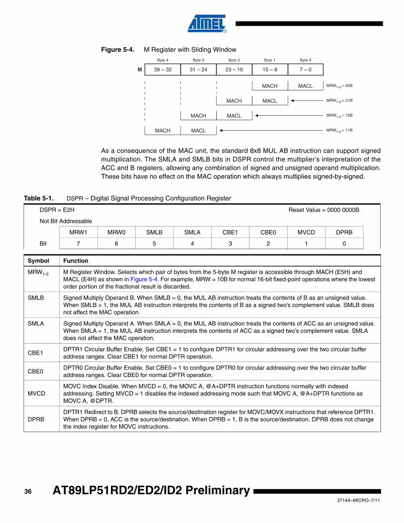
Figure 5-4. M Register with Sliding Window
As a consequence of the MAC unit, the standard 8x8 MUL AB instruction can support signedmultiplication. The SMLA and SMLB bits in DSPR control the multiplier’s interpretation of theACC and B registers, allowing any combination of signed and unsigned operand multiplication.These bits have no effect on the MAC operation which always multiplies signed-by-signed.
M 23 – 16 15 – 8 7 – 031 – 2439 – 32
Byte 4 Byte 3 Byte 2 Byte 1 Byte 0
MACH MACL
MACH MACL
MACH MACL
MACH MACL
MRW1-0 = 00B
MRW1-0 = 01B
MRW1-0 = 10B
MRW1-0 = 11B
Table 5-1. DSPR – Digital Signal Processing Configuration Register
DSPR = E2H Reset Value = 0000 0000B
Not Bit Addressable
MRW1 MRW0 SMLB SMLA CBE1 CBE0 MVCD DPRB
Bit 7 6 5 4 3 2 1 0
Symbol Function
MRW1-0 M Register Window. Selects which pair of bytes from the 5-byte M register is accessible through MACH (E5H) and MACL (E4H) as shown in Figure 5-4. For example, MRW = 10B for normal 16-bit fixed-point operations where the lowest order portion of the fractional result is discarded.
SMLB Signed Multiply Operand B. When SMLB = 0, the MUL AB instruction treats the contents of B as an unsigned value. When SMLB = 1, the MUL AB instruction interprets the contents of B as a signed two’s complement value. SMLB does not affect the MAC operation.
SMLA Signed Multiply Operand A. When SMLA = 0, the MUL AB instruction treats the contents of ACC as an unsigned value. When SMLA = 1, the MUL AB instruction interprets the contents of ACC as a signed two’s complement value. SMLA does not affect the MAC operation.
CBE1DPTR1 Circular Buffer Enable. Set CBE1 = 1 to configure DPTR1 for circular addressing over the two circular buffer address ranges. Clear CBE1 for normal DPTR operation.
CBE0DPTR0 Circular Buffer Enable. Set CBE0 = 1 to configure DPTR0 for circular addressing over the two circular buffer address ranges. Clear CBE0 for normal DPTR operation.
MVCDMOVC Index Disable. When MVCD = 0, the MOVC A, @A+DPTR instruction functions normally with indexed addressing. Setting MVCD = 1 disables the indexed addressing mode such that MOVC A, @A+DPTR functions as MOVC A, @DPTR.
DPRBDPTR1 Redirect to B. DPRB selects the source/destination register for MOVC/MOVX instructions that reference DPTR1. When DPRB = 0, ACC is the source/destination. When DPRB = 1, B is the source/destination. DPRB does not change the index register for MOVC instructions.
363714A–MICRO–7/11
AT89LP51RD2/ED2/ID2 Preliminary

AT89LP51RD2/ED2/ID2 Preliminary
5.4 Enhanced Dual Data PointersThe AT89LP51RD2/ED2/ID2 provides two 16-bit data pointers: DPTR0 and DPTR1. The datapointers are used by several instructions to access the program or data memories. TheAuxiliary 1 Register (AUXR1) and Data Pointer Configuration Register (DPCF) control operationof the dual data pointers (see Table 5-6 on page 39 and Table 5-7 on page 39). The DPS bit inAUXR1 selects which data pointer is currently referenced by instructions including the DPTRoperand. Each data pointer may also be accessed at a pair of SFR addresses that also dependon the DPS value. The data pointer referenced by DPS is located at the register pair DPL andDPH (82H an 83H), and the alternate data pointer not referenced by DPS is located at the regis-ter pair DPLB and DPHB (D4H and D5H). When DPS is toggled, the two data pointers also swapwhich SFR pair will access them as shown in Table 5-2. The AT89LP51RD2/ED2/ID2 providestwo methods for fast context switching of the data pointers:
• Bit 2 of AUXR1 is hard-wired as a logic 0. The DPS bit may be toggled (to switch data pointers) simply by incrementing the AUXR1 register, without altering other bits in the register unintentionally. This is the preferred method when only a single data pointer will be used at one time.EX: INC AUXR1 ; Toggle DPS
• In some cases, both data pointers must be used simultaneously. To prevent frequent toggling of DPS, the AT89LP51RD2/ED2/ID2 supports a prefix notation for selecting the opposite data pointer per instruction. All DPTR instructions, with the exception of JMP @A+DPTR, when prefixed with an 0A5H opcode will use the inverse value of DPS (DPS) to select the data pointer. Some assemblers may support this operation by using the /DPTR operand. For example, the following code performs a block copy within EDATA:
MOV AUXR1, #00H ; DPS = 0
MOV DPTR, #SRC ; load source address to dptr0
MOV /DPTR, #DST ; load destination address to dptr1
MOV R7, #BLKSIZE ; number of bytes to copy
COPY: MOVX A, @DPTR ; read source (dptr0)
INC DPTR ; next src (dptr0+1)
MOVX @/DPTR, A ; write destination (dptr1)
INC /DPTR ; next dst (dptr1+1)
DJNZ R7, COPY
For assemblers that do not support this notation, the 0A5H prefix must be declared in-line:
EX: DB 0A5H
INC DPTR ; equivalent to INC /DPTR
Table 5-2. Data Pointer Register Access
SFR DPS = 0 DPS = 1
DPL (82H) DP0L DP1L
DPH (83H) DP0H DP1H
DPLB (D4H) DP1L DP0L
DPHB (D5H) DP1H DP0H
373714A–MICRO–7/11

A summary of data pointer instructions with fast context switching is listed inTable 5-3.
5.4.1 Data Pointer UpdateThe Dual Data Pointers on the AT89LP51RD2/ED2/ID2 include two features that control howthe data pointers are updated. The data pointer decrement bits, DPD1 and DPD0 in AUXR1,configure the INC DPTR instruction to act as DEC DPTR. The resulting operation will depend onDPS as shown in Table 5-4. These bits also control the direction of auto-updates during MOVCand MOVX.
The data pointer update bits, DPU1 and DPU0, allow MOVX @DPTR and MOVC @DPTRinstructions to update the selected data pointer automatically in a post-increment or post-decre-ment fashion. The direction of update depends on the DPD1 and DPD0 bits as shown in Table5-5. These bits can be used to make block copy routines more efficient. Note that DPCF shouldbe cleared to zero, disabling these modes, before any calls are made to the Flash API.Caremust also be taken when interrupt routines use data pointers to ensure that correct operation issaved/restored correctly.
Table 5-3. Data Pointer Instructions
Instruction
Operation
DPS = 0 DPS = 1
JMP @A+DPTR JMP @A+DPTR0 JMP @A+DPTR1
MOV DPTR, #data16 MOV DPTR0, #data16 MOV DPTR1, #data16
MOV /DPTR, #data16 MOV DPTR1, #data16 MOV DPTR0, #data16
INC DPTR INC DPTR0 INC DPTR1
INC /DPTR INC DPTR1 INC DPTR0
MOVC A,@A+DPTR MOVC A,@A+DPTR0 MOVC A,@A+DPTR1
MOVC A,@A+/DPTR MOVC A,@A+DPTR1 MOVC A,@A+DPTR0
MOVX A,@DPTR MOVX A,@DPTR0 MOVX A,@DPTR1
MOVX A,@/DPTR MOVX A,@DPTR1 MOVX A,@DPTR0
MOVX @DPTR, A MOVX @DPTR0, A MOVX @DPTR1, A
MOVX @/DPTR, A MOVX @DPTR1, A MOVX @DPTR0, A
Table 5-4. Data Pointer Decrement Behavior
DPD1 DPD0
Equivalent Operation for INC DPTR and INC /DPTR
DPS = 0 DPS = 1
INC DPTR INC /DPTR INC DPTR INC /DPTR
0 0 INC DPTR0 INC DPTR1 INC DPTR1 INC DPTR0
0 1 DEC DPTR0 INC DPTR1 INC DPTR1 DEC DPTR0
1 0 INC DPTR0 DEC DPTR1 DEC DPTR1 INC DPTR0
1 1 DEC DPTR0 DEC DPTR1 DEC DPTR1 DEC DPTR0
383714A–MICRO–7/11
AT89LP51RD2/ED2/ID2 Preliminary

AT89LP51RD2/ED2/ID2 Preliminary
Table 5-5. Data Pointer Auto-Update
DPD1 DPD0
Update Operation for MOVX and MOVC (DPU1 = 1 & DPU0 = 1)
DPS = 0 DPS = 1
DPTR /DPTR DPTR /DPTR
0 0 DPTR0++ DPTR1++ DPTR1++ DPTR0++
0 1 DPTR0-- DPTR1++ DPTR1++ DPTR0--
1 0 DPTR0++ DPTR1-- DPTR1-- DPTR0++
1 1 DPTR0-- DPTR1-- DPTR1-- DPTR0--
Table 5-6. AUXR1 – Auxiliary Register 1
AUXR1 = A2H Reset Value = XXX0 00X0B
Not Bit Addressable
– – ENBOOT XSTK GF3 0 – DPS
Bit 7 6 5 4 3 2 1 0
Symbol Function
ENBOOT Set ENBOOT = 1 to map the Boot ROM in the range F800H–FFFFH. This is required to run the bootloader or access the Flash API. When ENBOOT = 0 the Boot ROM is not accessible and normal program memory is mapped to this range. The default value is set by the Bootloader Jump bit. See Section 24.2 on page 190.
XSTK Extended Stack Enable. When XSTK = 0 the stack resides in IDATA and is limited to 256 bytes. Set XSTK = 1 to place the stack in EDATA for up to 2K bytes of extended stack space. All PUSH, POP, CALL and RET instructions will incur a one or two cycle penalty when accessing the extended stack.
GF3 This bit is a general purpose user flag.
DPS Data Pointer Select. DPS selects the active data pointer for instructions that reference DPTR. When DPS = 0, DPTR will target DPTR0 and /DPTR will target DPTR1. When DPS = 1, DPTR will target DPTR1 and /DPTR will target DPTR0.
Table 5-7. DPCF – Data Pointer Configuration Register
DPCF = A1H Reset Value = 0000 XXXXB
Not Bit Addressable
DPU1 DPU0 DPD1 DPD0 – – – –
Bit 7 6 5 4 3 2 1 0
Symbol Function
DPU1 Data Pointer 1 Update. When set, MOVX @DPTR and MOVC @DPTR instructions that use DPTR1 will also update DPTR1 based on DPD1. If DPD1 = 0 the operation is post-increment and if DPD1 = 1 the operation is post-decrement. When DPU1 = 0, DPTR1 is not updated.
DPU0 Data Pointer 0 Update. When set, MOVX @DPTR and MOVC @DPTR instructions that use DPTR0 will also update DPTR0 based on DPD0. If DPD0 = 0 the operation is post-increment and if DPD0 = 1 the operation is post-decrement. When DPU0 = 0, DPTR0 is not updated.
DPD1 Data Pointer 1 Decrement. When set, INC DPTR instructions targeted to DPTR1 will decrement DPTR1. When cleared, INC DPTR instructions will increment DPTR1. DPD1 also determines the direction of auto-update for DPTR1 when DPU1 = 1.
DPD0 Data Pointer 0 Decrement. When set, INC DPTR instructions targeted to DPTR0 will decrement DPTR0. When cleared, INC DPTR instructions will increment DPTR0. DPD0 also determines the direction of auto-update for DPTR0 when DPU0 = 1.
393714A–MICRO–7/11

5.4.2 Data Pointer Operating ModesThe Dual Data Pointers on the AT89LP51RD2/ED2/ID2 include three additional operatingmodes that affect data pointer based instructions. These modes are controlled by bits in DSPR.Note that these bits in DSPR should be cleared to zero, disabling these modes, before any callsare made to the Flash API.Care must also be taken when interrupt routines use data pointers toensure that correct operation is saved/restored correctly.
5.4.2.1 DPTR RedirectThe Data Pointer Redirect to B bit, DPRB (DSPR.0), allows MOVX and MOVC instructions touse the B register as the data source/destination when the instruction references DPTR1 asshown in Table 5-8 and Table 5-9. DPRB can improve the efficiency of routines that must fetchmultiple operands from different RAM locations.
5.4.2.2 Index DisableThe MOVC Index Disable bit, MVCD (DSPR.1), disables the indexed addressing mode of theMOVC A, @A+DPTR instruction. When MVCD = 1, the MOVC instruction functions asMOVC A, @DPTR with no indexing as shown in Table 5-9. MVCD can improve the efficiency ofroutines that must fetch multiple operands from program memory. DPRB can change the MOVCdestination register from ACC to B, but has no effect on the MOVC index register.
Table 5-8. MOVX @DPTR Operating Modes
DPRB DPS
Equivalent Operation for MOVX
MOVX A, @DPTR MOVX @DPTR, A
DPTR /DPTR DPTR /DPTR
0 0MOVX
A, @DPTR0MOVX
A, @DPTR1MOVX
@DPTR0, AMOVX
@DPTR1, A
0 1MOVX
A, @DPTR1MOVX
A, @DPTR0MOVX
@DPTR1, AMOVX
@DPTR0, A
1 0MOVX
A, @DPTR0MOVX
B, @DPTR1MOVX
@DPTR0, AMOVX
@DPTR1, B
1 1MOVX
B, @DPTR1MOVX
A, @DPTR0MOVX
@DPTR1, BMOVX
@DPTR0, A
Table 5-9. MOVC @DPTR Operating Modes
MVCD DPRB
Equivalent Operation for MOVC A, @A+DPTR
DPS = 0 DPS = 1
DPTR /DPTR DPTR /DPTR
0 0MOVC
A, @A+DPTR0MOVC
A, @A+DPTR1MOVC
A, @A+DPTR1MOVC
A, @A+DPTR0
0 1MOVC
A, @A+DPTR0MOVC
B, @A+DPTR1MOVC
B, @A+DPTR1MOVC
A, @A+DPTR0
1 0MOVC
A, @DPTR0MOVC
A, @DPTR1MOVC
A, @DPTR1MOVC
A, @DPTR0
1 1MOVC
A, @DPTR0MOVC
B, @DPTR1MOVC
B, @DPTR1MOVC
A, @DPTR0
403714A–MICRO–7/11
AT89LP51RD2/ED2/ID2 Preliminary

AT89LP51RD2/ED2/ID2 Preliminary
5.4.2.3 Circular BuffersThe CBE0 and CBE1 bits in DSPR can configure DPTR0 and DPTR1, respectively, to operate incircular buffer mode. The AT89LP51RD2/ED2/ID2 maps circular buffers into two identicallysized regions of EDATA/XDATA. These buffers can speed up convolution computations such asFIR and IAR digital filters. The length of the buffers are set by the value of the FIRD (E3H) regis-ter for up to 256 entries. Buffer A is mapped from 0000H to FIRD and Buffer B is mapped from0100H to 100H+FIRD as shown in Figure 5-5. Both data pointers may operate in either buffer.When circular buffer mode is enabled, updates to a data pointer referencing the buffer region willfollow circular addressing rules. If the data pointer is equal to FIRD or 100H+FIRD any incre-ment will cause it to overflow to 0000H or 0100H respectively. If the data pointer is equal to0000H or 0100H any decrement will cause it to underflow to FIRD or 100H+FIRD respectively.In this mode, updates can be either an explicit INC DPTR or an automatic update using DPUnwhere the DPDn bits control the direction. The data pointer will increment or decrement normallyat any other addresses. Therefore, when circular addressing is in use, the data pointers can stilloperate as regular pointers in the FIRD+1 to 00FFH and greater than 100H+FIRD ranges.
Figure 5-5. Circular Buffer Mode
5.5 Instruction Set ExtensionsTable 5-10 lists the additions to the 8051 instruction set that are supported by theAT89LP51RD2/ED2/ID2. For more information on the instruction set see Section 22. “InstructionSet Summary” on page 175. For detailed descriptions of the extended instructions see Section22.1 “Instruction Set Extensions” on page 179.
0000h
DPTR
0100h
FIRD
100h + FIRD
DPTR
DP
Dn
= 0
DP
Dn
= 1
DP
Dn
= 0
DP
Dn
= 1A
B
Table 5-10. AT89LP51RD2/ED2/ID2 Extended Instructions
Opcode Mnemonic Description Bytes Cycles
A5 00 BREAK Software breakpoint 2 2
A5 03 ASR M Arithmetic shift right of M register 2 2
A5 23 LSL M Logical shift left of M register 2 2
A5 73 JMP @A+PC Indirect jump relative to PC 2 3
A5 90 MOV /DPTR, #data16Move 16-bit constant to alternate data pointer
4 4
A5 93 MOVC A, @A+/DPTRMove code location to ACC relative to alternate data pointer
2 4
A5 A3 INC /DPTR Increment alternate data pointer 2 3
413714A–MICRO–7/11

• The /DPTR instructions provide support for the dual data pointer features described above (See Section 5.4).
• The ASR M, LSL M, CLR M and MAC AB instructions are part of the Multiply-Accumulate Unit (See Section 5.3).
• The JMP @A+PC instruction supports localized jump tables without using a data pointer.
• The CJNE A, @Ri, rel instructions allow compares of array values with non-constant values.
• The BREAK instruction is used by the On-Chip Debug system. See Section 23. on page 185.
• Some third party assemblers/compilers do not support these instructions. In order to use them you may need to write assembly functions that emulate the instruction by declaring the opcodes inline as shown in Table 5-11.
A5 A4 MAC AB Multiply and accumulate 2 9
A5 B6 CJNE A, @R0, relCompare ACC to indirect RAM and jump if not equal
3 4
A5 B7 CJNE A, @R1, relCompare ACC to indirect RAM and jump if not equal
3 4
A5 E0 MOVX A, @/DPTRMove external to ACC; 16-bit address in alternate data pointer
2 3/5
A5 E4 CLR M Clear M register 2 2
A5 F0 MOVX @/DPTR, AMove ACC to external; 16-bit address in alternate data pointer
2 3/5
Table 5-11. Extended Instruction Assembly Emulations
Opcode Mnemonic Emulation
A5 00 BREAK DB A5H, 00H
A5 03 ASR M DB A5H, 03H or DB A5H followed by RR A
A5 23 LSL M DB A5H, 23H or DB A5H followed by RL A
A5 73 JMP @A+PC DB A5H, 73H or DB A5H followed by JMP @A+DPTR
A5 90 MOV /DPTR, #data16 DB A5H followed by MOV DPTR, #data16
A5 93 MOVC A, @A+/DPTR DB A5H, 93H or DB A5H followed by MOVC A, @A+DPTR
A5 A3 INC /DPTR DB A5H, A3H or DB A5H followed by INC DPTR
A5 A4 MAC AB DB A5H, A4H or DB A5H followed by MUL AB
A5 B6 CJNE A, @R0, rel DB A5H, B6H, (LABEL-$-3) where LABEL is the jump target
A5 B7 CJNE A, @R1, rel DB A5H, B7H, (LABEL-$-3) where LABEL is the jump target
A5 E0 MOVX A, @/DPTR DB A5H, E0H or DB A5H followed by MOVX A, @DPTR
A5 E4 CLR M DB E4H, E0H or DB A5H followed by CLR A
A5 F0 MOVX @/DPTR, A DB A5H, F0H or DB A5H followed by MOVX @DPTR, A
Table 5-10. AT89LP51RD2/ED2/ID2 Extended Instructions
Opcode Mnemonic Description Bytes Cycles
423714A–MICRO–7/11
AT89LP51RD2/ED2/ID2 Preliminary

AT89LP51RD2/ED2/ID2 Preliminary
6. System ClockThe AT89LP51RD2/ED2 has a single system clock that is generated directly from one of threeselectable clock sources: on-chip crystal oscillator A in high or low power operation, externalclock source on XTAL1A, and the internal 8 MHz RC oscillator. A diagram of the clock subsys-tem is shown in Figure 6-1. The clock source is selected by the Clock Source A User Fuses asshown in Table 6-1 (See “User Configuration Fuses” on page 190). In addition to this systemclock, the AT89LP51ID2 device adds a second system clock source that is selectable from on-chip low frequency crystal oscillator B in, external clock source on XTAL1B, and the internal 8MHz RC oscillator. A diagram of this clock subsystem is shown in Figure 6-2. Clock source B isselected by the Clock Source B User Fuses as shown in Table 6-2. The choice of clock sourcealso affects the start-up time after a POR, BOD or Power-down event (See “Reset” on page 53or “Power-down Mode” on page 58).
The AT89LP51RD2/ED2/ ID2 inc ludes a X1 /X2 fea tu re fo r compa t i b i l i t y w i thAT89C51RD2/ED2/ID2. This feature determines if the oscillator source is divided by two or notto generate the system clock. The 8-bit system clock divider may be used to prescale the systemclock to reduce the operating frequency. In addition a 4-bit prescaler is available to change theclocks of the peripherals.
Figure 6-1. AT89LP51RD2/ED2 Clock Subsystem Diagram
Figure 6-2. AT89LP51ID2 Clock Subsystem Diagram
XTAL1A
XTAL2ASYSTEM CLOCK
(CLKSYS)
INTERNAL8.0 MHz
OSC0
1
2
3
8-BITCLOCK
DIVIDER
CLKIRC
CLKEXT
CLKXTAL
CLOCK FUSE A
4-BITPRESCALER
TPS3-0
Timer 0Timer 1Timer 2PCAWatchdog
÷2 0
1
X2 (CKCON0.0)
CKRL
0
1
CKRL != FFH
OSCA
XTAL1A
XTAL2A
SYSTEM CLOCK(CLKSYS)
INTERNAL8.0 MHz
OSC0
1
2
3
8-BITCLOCK
DIVIDER
CLKIRC
CLKEXTA
CLKXTALA
CLOCK FUSE A
4-BITPRESCALER
TPS3-0
Timer 0Timer 1Timer 2PCAWatchdog
÷2 0
1
X2 (CKCON0.0)
CKRL
0
1
CKRL != FFHOSCA
XTAL1B
XTAL2B
0
1
2
3
CLKIRC
CLKEXTB
CLKXTALB
CLOCK FUSE B
OSCB
OscAEn (OSCON.0)
OscBEn (OSCON.1)
0
1
CKS (CKSEL.0)
÷128 Timer 0 Subclock
Timer 2 (EXTB or XTALB only via T2 )
433714A–MICRO–7/11

6.1 Crystal Oscillator AWhen enabled, internal inverting oscillator amplifier A is connected between XTAL1A andXTAL2A for connection to an external quartz crystal or ceramic resonator. The oscillator mayoperate in either high-speed or low-power mode. Low-power mode is intended for crystals of 12MHz or less and consumes less power than the higher speed mode. The configuration as shownin Figure 6-3 applies for both high and low power oscillators. Note that in some cases, externalcapacitors C1 and C2 may be reduced due to the on-chip capacitance of the XTAL1A andXTAL2A inputs (approximately 10 pF each). When using the crystal oscillator, P4.6 and P4.7 willhave their inputs and outputs disabled. Also, XTAL2A in crystal oscillator mode should not beused to directly drive a board-level clock without a buffer.
An optional 5 MΩ on-chip resistor can be connected between XTAL1A and GND. This resistorcan improve the startup characteristics of the oscillator especially at higher frequencies. Theresistor can be enabled/disabled with the R1 User Fuse (See “User Configuration Fuses” onpage 190.)
Figure 6-3. Crystal Oscillator A Connections
Note: 1. C1, C2 = 5–15 pF for Crystals= 5–15 pF for Ceramic Resonators
Table 6-1. Clock Source A Settings
Clock Source AFuse 1
Clock Source AFuse 0 Selected Clock Source
1 1 High Speed Crystal Oscillator A (f > 12 MHz)
1 0 Low Power Crystal Oscillator A (f ≤ 12 MHz)
0 1 External Clock on XTAL1A
0 0 Internal 8.0 MHz RC Oscillator
Table 6-2. Clock Source B Settings (AT89LP51ID2 Only)
Clock Source BFuse 1
Clock Source BFuse 0 Selected Clock Source
1 – Low Frequency Crystal Oscillator B (32 kHz)
0 1 External Clock on XTAL1B
0 0 Internal 8.0 MHz RC Oscillator
~10 pF
~10 pF
C2
C1
R1~5 MΩ
443714A–MICRO–7/11
AT89LP51RD2/ED2/ID2 Preliminary

AT89LP51RD2/ED2/ID2 Preliminary
6.2 External Clock Source AThe external clock option disables the oscillator amplifier and allows XTAL1A to be drivendirectly by an external clock source as shown in Figure 6-4. XTAL2A may be left unconnected,used as general purpose I/O P4.7, or configured to output a divided version of the system clock.
Figure 6-4. External Clock A Drive Configuration
6.3 Internal RC OscillatorThe AT89LP51RD2/ED2/ID2 has an Internal RC oscillator tuned to 8.0 MHz ±2.5%. Whenenabled as clock source A, XTAL1A and XTAL2A may be used as P4.6 and P4.7 respectively.For AT89LP51ID2 the internal oscillator can also be selected for clock source B, freeing upXTAL1B and XTAL2B to act as P1.0 and P4.2 respectively. The frequency of the oscillator maybe adjusted within limits by changing the RC Calibration Byte stored at byte 384 of the User Sig-nature Array. This location may be updated using the IAP interface or by an external deviceprogrammer (User Signature location 0180H). See Section 24.1.2 “Atmel Signature Array” onpage 190. A copy of the factory calibration byte is stored at byte 8 of the Atmel Signature Array(0008H in SIG space).
6.4 Crystal Oscillator B (AT89LP51ID2)AT89LP51ID2 includes a second crystal oscillator for low-frequency (~32 KHz) operation. Whenenabled, internal inverting oscillator amplifier B is connected between XTAL1B and XTAL2B forconnection to an external quartz crystal or ceramic resonator as shown in Figure 6-5. Note thatin some cases, external capacitors C1 and C2 may be reduced due to the on-chip capacitanceof the XTAL1B and XTAL2B inputs (approximately 10 pF each). An on-chip series resistance isincluded between the amplifier and the XTAL2B pad to limit the drive level. In most cases anexternal series resistor is not required. When using the crystal oscillator, P1.0 and P4.2 will havetheir inputs and outputs disabled. Also, XTAL2B in crystal oscillator mode should not be used todirectly drive a board-level clock without a buffer.
Please note that the low-frequency oscillator may have a very long settling time. The systemmust ensure that the oscillator has sufficient time to stabilize before the device is allowed tooperate from this clock source.
XT AL2A (P4.7)
XT AL1A (P4.6)
GND
NC GPIO
EXTERNAL OSCILLA T OR
SIGNAL
453714A–MICRO–7/11
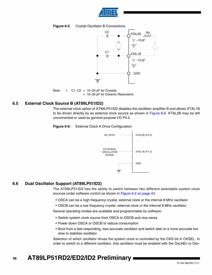
Figure 6-5. Crystal Oscillator B Connections
Note: 1. C1, C2 = 10–20 pF for Crystals= 10–20 pF for Ceramic Resonators
6.5 External Clock Source B (AT89LP51ID2)The external clock option of AT89LP51ID2 disables the oscillator amplifier B and allows XTAL1Bto be driven directly by an external clock source as shown in Figure 6-6. XTAL2B may be leftunconnected or used as general purpose I/O P4.2.
Figure 6-6. External Clock A Drive Configuration
6.6 Dual Oscillator Support (AT89LP51ID2)The AT89LP51ID2 has the ability to switch between two different selectable system clocksources under software control as shown in Figure 6-2 on page 43.
• OSCA can be a high frequency crystal, external clock or the internal 8 MHz oscillator
• OSCB can be a low frequency crystal, external clock or the internal 8 MHz oscillator
Several operating modes are available and programmable by software:
• Switch system clock source from OSCA to OSCB and vice-versa
• Power down OSCA or OSCB to reduce consumption
• Boot from a fast responding, less accurate oscillator and switch later to a more accurate but slow to stabilize oscillator.
Selection of which oscillator drives the system clock is controlled by the CKS bit in CKSEL. Inorder to switch to a different oscillator, that oscillator must be enabled with the OscAEn or Osc-
~10 pF
~10 pF
C2 Rd
C1
XTAL2B
XTAL1B
XT AL2B (P4.2)
XT AL1B (P1.0)
GND
NC GPIO
EXTERNAL OSCILLA T OR
SIGNAL
463714A–MICRO–7/11
AT89LP51RD2/ED2/ID2 Preliminary
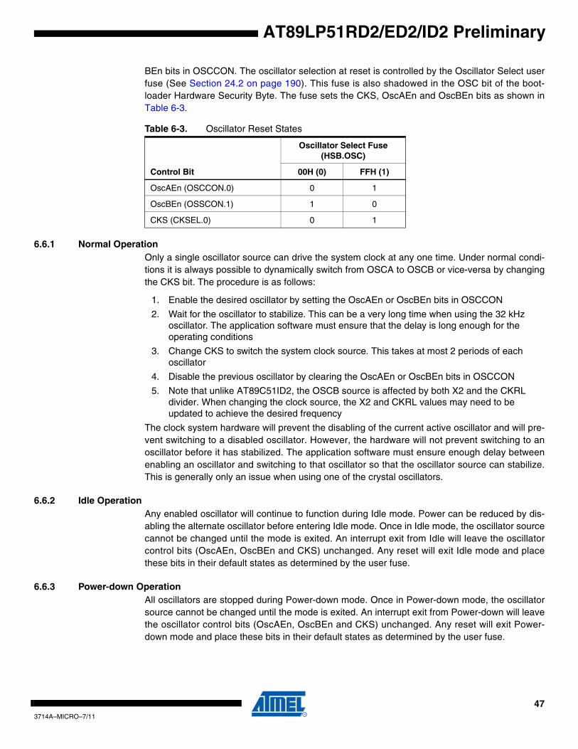
AT89LP51RD2/ED2/ID2 Preliminary
BEn bits in OSCCON. The oscillator selection at reset is controlled by the Oscillator Select userfuse (See Section 24.2 on page 190). This fuse is also shadowed in the OSC bit of the boot-loader Hardware Security Byte. The fuse sets the CKS, OscAEn and OscBEn bits as shown inTable 6-3.
6.6.1 Normal OperationOnly a single oscillator source can drive the system clock at any one time. Under normal condi-tions it is always possible to dynamically switch from OSCA to OSCB or vice-versa by changingthe CKS bit. The procedure is as follows:
1. Enable the desired oscillator by setting the OscAEn or OscBEn bits in OSCCON
2. Wait for the oscillator to stabilize. This can be a very long time when using the 32 kHz oscillator. The application software must ensure that the delay is long enough for the operating conditions
3. Change CKS to switch the system clock source. This takes at most 2 periods of each oscillator
4. Disable the previous oscillator by clearing the OscAEn or OscBEn bits in OSCCON
5. Note that unlike AT89C51ID2, the OSCB source is affected by both X2 and the CKRL divider. When changing the clock source, the X2 and CKRL values may need to be updated to achieve the desired frequency
The clock system hardware will prevent the disabling of the current active oscillator and will pre-vent switching to a disabled oscillator. However, the hardware will not prevent switching to anoscillator before it has stabilized. The application software must ensure enough delay betweenenabling an oscillator and switching to that oscillator so that the oscillator source can stabilize.This is generally only an issue when using one of the crystal oscillators.
6.6.2 Idle OperationAny enabled oscillator will continue to function during Idle mode. Power can be reduced by dis-abling the alternate oscillator before entering Idle mode. Once in Idle mode, the oscillator sourcecannot be changed until the mode is exited. An interrupt exit from Idle will leave the oscillatorcontrol bits (OscAEn, OscBEn and CKS) unchanged. Any reset will exit Idle mode and placethese bits in their default states as determined by the user fuse.
6.6.3 Power-down OperationAll oscillators are stopped during Power-down mode. Once in Power-down mode, the oscillatorsource cannot be changed until the mode is exited. An interrupt exit from Power-down will leavethe oscillator control bits (OscAEn, OscBEn and CKS) unchanged. Any reset will exit Power-down mode and place these bits in their default states as determined by the user fuse.
Table 6-3. Oscillator Reset States
Control Bit
Oscillator Select Fuse(HSB.OSC)
00H (0) FFH (1)
OscAEn (OSCCON.0) 0 1
OscBEn (OSSCON.1) 1 0
CKS (CKSEL.0) 0 1
473714A–MICRO–7/11
6.6.4 Registers
6.7 X1/X2 FeatureThe AT89LP51RD2/ED2/ID2 includes the X1/X2 feature for compatibility with the existingAT89C51RD2/ED2/ID2. This feature allows a divider-by-2 to be switched in/out between theoscillator source and the main system clock. This feature is controlled by the X2 bit in CKCON0(See Table 6-9 on page 50). When X2 = 0 the system clock is divided by two from the oscillatorsource, ensuring a 50% duty cycle regardless of the cyclic ratio at the oscillator output. WhenX2 = 1 the oscillator output is passed through with no division. In this case the duty cycle at theoscillator must be between 40% and 60%. Note that the naming convention can be confusingsince X1 means divide-by-2 and X2 means divide-by-1 as shown in Table 6-7. The default stateof the X2 bit is set by the X2 User fuse (See Section 24.2 on page 190) but can always bechanged by software. This fuse is also shadowed in the X2 bit of the bootloader Hardware Secu-rity Byte (HSB). Note that the fuse/HSB bit is inverted from the control bit in the CKCON0 SFR.
Table 6-4. CKSEL – Clock Selection Register
CKSEL = 85H (AT89LP51ID2 Only) Reset Value = XXXX XXX?B
Not Bit Addressable
– – – – – – – CKS
Bit 7 6 5 4 3 2 1 0
Symbol Function
CKS Clock Select. Clear CKS to connect the system clock (CPU and peripherals) to the OSCB source. Set CKS to connect the system clock to the OSCA source. The default state is set by the Oscillator Select user fuse. See Section 24.2 on page 190.
Table 6-5. OSCCON – Oscillator Control Register
OSCCON = 86H (AT89LP51ID2 Only) Reset Value = XXXX X0??B
Not Bit Addressable
– – – – – SCLKT0 OscBEn OscAEn
Bit 7 6 5 4 3 2 1 0
Symbol Function
SCLKT0 Sub Clock Timer 0. Clear to connect the Timer 0 counter input to T0 (P3.4). Set to connect the Timer 0 counter input to OSCB output divided by 128. OSCB must be sourced from crystal oscillator B to use this feature.
OscBEn OSCB Enable. Clear to power down the OSCB source. Set to enable the OSCB source. The default state is set by the Oscillator Select user fuse. See Section 24.2 on page 190. OscBEn cannot be disabled when CKS = 0. Disabling OSCB will free the XTAL1B and XTAL2B pins for use as P1.0 and P4.2.
OscAEn OSCA Enable. Clear to power down the OSCA source. Set to enable the OSCA source. The default state is set by the Oscillator Select user fuse. See Section 24.2 on page 190. OscAEn cannot be disabled when CKS = 1.
Table 6-6. X1/X2 Modes
ModeX2
(CKCON0.0) CPU ClockXTAL1
Duty CycleX2 Fuse(HSB.X2)
X1 0 fCPU = fSYS/2 No limits FFH (1)
X2 1 fCPU = fSYS/1 40–60% 00H (0)
483714A–MICRO–7/11
AT89LP51RD2/ED2/ID2 Preliminary

AT89LP51RD2/ED2/ID2 Preliminary
6.8 System Clock PrescalerThe AT89LP51RD2/ED2/ID2 includes an 8-bit prescaler that allows the system clock to bedivided down from the selected clock source by even numbers in the range 4–1020 in X1 modeand 2–510 in X2 mode. The prescaler can reduce power consumption by decreasing the opera-tional frequency during non-critical periods. The prescaler is implemented as an 8-bit counterwith reload. Upon overflow from FFH to 00H the counter is reloaded with the value of the CKRLregister. When CKRL = FFH the prescaler is disabled. The resulting system frequency is givenby the following equations where fOSC is the frequency of the selected clock source and X2 is thevalue of CKCON0.0:
The clock divider will prescale the clock for the CPU and all peripherals. The value of CKRL maybe changed at any time without interrupting normal execution. Changes to CKRL will take affecton the next prescaler overflow. When CKRL is updated, the new frequency will take affect withina maximum period of 1024 x tOSC. The prescaler is disabled by reset.
fSYSfOSC 2X2×
4 255 CKRL–( )×-----------------------------------------------= CKRL 255<( )
fSYSfOSC 2X2×
2----------------------------= CKRL 255=( )
Table 6-7. CKRL – Clock Reload Register
CKRL = 97H Reset Value = 1111 1111B
Not Bit Addressable
CKRL7 CKRL6 CKRL5 CKRL4 CKRL3 CKRL2 CKRL1 CKRL0
Bit 7 6 5 4 3 2 1 0
Symbol Function
CKRL7-0 Clock Reload. CKRL holds the reload value for the 8-bit system clock prescaler. When CKRL = FFH the prescaler is disabled and no division is used. For all other values, the prescaler counts up to FFH and is reloaded with the value of CKRL on the overflow to 00H. Each overflow of the prescaler will toggle the system clock. Changes to CKRL will take affect on the next overflow.
Table 6-8. CLKREG – Clock Register
CLKREG = AEH Reset Value = 0101 XXXXB
Not Bit Addressable
TPS3 TPS2 TPS1 TPS0 — — — —
Bit 7 6 5 4 3 2 1 0
Symbol Function
TPS3-0 Timer Prescaler. The Timer Prescaler selects the time base for Timer 0, Timer 1, Timer 2, PCA and the Watchdog Timer. The prescaler is implemented as a 4-bit binary down counter. When the counter reaches zero it is reloaded with the value stored in the TPS bits to give a division ratio between 1 and 16. By default TPS is set to 5 for counting every six cycles (AT89C51RD2/ED2/ID2 compatibility). The prescaler is always enabled in Compatibility mode. In Fast mode the prescaler is off by default and can be individually enabled for the peripherals through the CKCON0 and CKCON1 SFRs.
493714A–MICRO–7/11

6.9 Peripheral ClocksThe base peripheral clock is the same as the CPU clock. It is affected by both the X2 setting andthe CKRL prescaler. However, individual peripherals can have their clock further modified usingthe Timer Prescaler in the CLKREG register and the clock selection bits in the CKCON0 andCKCON1 registers. The Timer Prescaler is a 4-bit prescaler controlled by the TPS bits inCLKREG (See Table 6-8 on page 49). This prescaler is shared among all peripherals and con-trols the counting rate of Timer 0, Timer 1, Timer 2, the PCA Timer and the Watchdog. By defaultthe timers will count every CPU clock cycle in Fast mode (TPS = 0000B) and every six CPUcycles in Compatibility mode (TPS = 0101B).
The bits in CKCON0 and CKCON1 select how the Timer Prescaler affects each peripheral. InCompatibility mode these bits decide if a further divide-by-two is included in addition to the pres-caler. This allows a device in X2 mode to use peripherals that still run in X1 mode, i.e. X2 can beenabled to speed up the CPU without needing to update the peripheral baud rates, overflowperiods, etc. Peripherals not affected by the Timer Prescaler switch between the CPU clock andthe CPU clock divided-by-2.
In Fast Mode the bits in CKCON0 and CKCON1 turn the Timer Prescaler on/off for each periph-eral. The following equations show the peripheral clock rates in Compatibility Mode and FastMode where ?X2 is a peripherals bit in CKCON0 or CKCON1.
An overview of the peripheral clock selection is given in Figure 6-7 on page 51.
fPERIPHERALfCPU
2?X2 TPS 1+( )×---------------------------------------------= Compatibility Mode
fPERIPHERALfCPU
TPS 1+---------------------= Fast Mode and ?X2 = 1
Table 6-9. CKCON0 – Clock Control Register 0
CKCON0 = 8FH Reset Value = 0000 000?B
Not Bit Addressable
TWIX2 WDX2 PCAX2 SIX2 T2X2 T1X2 T0X2 X2
Bit 7 6 5 4 3 2 1 0
Symbol Function
TWIX2 Two-Wire Clock. In Compatibility Mode, clear for one system clock period per peripheral clock cycle and set for two clock periods per peripheral clock cycle (only valid when X2 = 1). In Fast Mode, clear for one system clock period and set for TPS+1 clocks per peripheral clock cycle. This bit only affects the generated SCL rate during TWI master mode.
WDX2Watchdog Clock. In Compatibility Mode, clear for TPS+1 system clock periods per peripheral clock cycle and set for 2(TPS+1) clock periods per peripheral clock cycle. In Fast Mode, clear for one system clock period and set for TPS+1 clocks per peripheral clock cycle. This bit affects the watchdog timeout period.
PCAX2 Programmable Counter Array Clock. This bit affects the PCA timer increment rate and depends on CPS in CMOD.
CPS1-0 = 00B: In Compatibility Mode, clear for TPS+1 system clock periods per peripheral clock cycle and set for 2(TPS+1) clock periods per peripheral clock cycle. In Fast Mode, clear for one system clock period and set for TPS+1 clocks per peripheral clock cycle. CPS1-0 = 01B: In Compatibility Mode, clear for one system clock period per peripheral clock cycle and set for two clock periods per peripheral clock cycle. In Fast Mode, clear for one system clock period and set for TPS+1 clocks per peripheral clock cycle.
503714A–MICRO–7/11
AT89LP51RD2/ED2/ID2 Preliminary

AT89LP51RD2/ED2/ID2 Preliminary
Figure 6-7. Peripheral Clock Selection
SIX2 UART Clock. In Compatibility Mode, clear for one system clock period per peripheral clock cycle and set for two clock periods per peripheral clock cycle (only valid when X2 = 1). In Fast Mode, clear for one system clock period and set for TPS+1 clocks per peripheral clock cycle. This bit affects the generated baud rate during modes 0 and 2.
T2X2 Timer 2 Clock. In Compatibility Mode, clear for TPS+1 system clock periods per peripheral clock cycle and set for 2(TPS+1) clock periods per peripheral clock cycle. In Fast Mode, clear for one system clock period and set for TPS+1 clocks per peripheral clock cycle. This bit affects the timer increment/decrement rate.
T1X2 Timer 1 Clock. In Compatibility Mode, clear for TPS+1 system clock periods per peripheral clock cycle and set for 2(TPS+1) clock periods per peripheral clock cycle. In Fast Mode, clear for one system clock period and set for TPS+1 clocks per peripheral clock cycle. This bit affects the timer increment rate.
T0X2 Timer 0 Clock. In Compatibility Mode, clear for TPS+1 system clock periods per peripheral clock cycle and set for 2(TPS+1) clock periods per peripheral clock cycle. In Fast Mode, clear for one system clock period and set for TPS+1 clocks per peripheral clock cycle. This bit affects the timer increment rate.
X2 CPU Clock. In Compatibility Mode, clear for 12 clock periods per machine cycle and set for 6 clock periods per machine cycle. In Fast Mode, clear for two clock periods per instruction cycle and set for one clock periods per instruction cycle. The default state of X2 is set by the X2 Fuse. See Section 24.2 on page 190.
Symbol Function
SYSTEM CLOCK ÷2
0
1
T0X2
÷(TPS+1)Timer 0
÷2
0
1Timer 1
T1X2
0
1Timer 2
T2X2
0
1Watchdog
WDX2
0
1PCA(CPS = 00B)
PCAX2
0
1PCA(CPS = 01B)
PCAX2
SIX2 & X2
UART0
1
SPIX2 & X2
SPI0
1
TWIX2 & X2
TWI0
1
SYSTEM CLOCK
0
1
T0X2
÷(TPS+1)Timer 0
÷2
0
1Timer 1
T1X2
0
1Timer 2
T2X2
0
1Watchdog
WDX2
0
1PCA(CPS = 00B)
PCAX2
0
1PCA(CPS = 01B)
PCAX2
SIX2 & X2
UART0
1
SPIX2 & X2
SPI0
1
TWIX2 & X2
TWI0
1
Fast ModeCompatibility Mode
513714A–MICRO–7/11

6.10 Timer Subclock (AT89L51ID2)When OSCB of AT89LP51ID2 is enabled and sourced from the low-frequency crystal oscillator,it can drive the counter input of Timer 0 in place of the T0 pin by setting the SCLKT0 bit in OSC-CON. The counter input will be toggled at the oscillator frequency divided by 128. For this modeto function correctly, the timer peripheral clock must be running (not in Power-down) and operat-ing at a frequency at least twice as high as the subclock as shown in the following equation:
This requirement is due to the fact that the timer must still sample the subclock edges the sameas if were sampling the T0 pin. This feature is not available when OSCB is sourced from eitherthe external clock on XTAL1B or the internal oscillator.
Pin T2 is also shared with the XTAL1B pin. When OSBC is enabled in the crystal oscillator orexternal clock modes, T2 will toggle at the oscillator frequency. Timer 2 can then use the oscilla-tor as its counter input as well, with no division. For this mode to function correctly, the timerperipheral clock must be running (not in Power-down) and operating at a frequency at leasttwice as high OSCB as shown in the following equation:
Table 6-10. CKCON1 – Clock Control Register 1
CKCON1 = AFH Reset Value = XXXX XXX0B
Not Bit Addressable
– – – – – – – SPIX2
Bit 7 6 5 4 3 2 1 0
Symbol Function
SPIX2 SPI Clock. In Compatibility Mode, clear for one system clock period per peripheral clock cycle and set for two clock periods per peripheral clock cycle (only valid when X2 = 1). In Fast Mode, clear for one system clock period and set for TPS+1 clocks per peripheral clock cycle. This bit only affects the generated SCK rate during SPI master mode.
Timer 0 Subclock: fTIMER0
fXTAL1B
64-------------------≥
Timer 2 Subclock: fTIMER2 fXTAL1B 2×≥
523714A–MICRO–7/11
AT89LP51RD2/ED2/ID2 Preliminary

AT89LP51RD2/ED2/ID2 Preliminary
7. ResetDuring reset, all I/O Registers are set to their initial values, the port pins are set to their defaultmode, and the p rogram s ta r ts execu t i on f rom the Rese t Vec to r , 0000H. TheAT89LP51RD2/ED2/ID2 has six sources of reset: power-on reset, brown-out reset, externalreset, hardware watchdog reset, PCA watchdog reset and software reset.
Figure 7-1. Reset Subsystem Diagram
7.1 Power-on ResetA Power-on Reset (POR) is generated by an on-chip detection circuit. The detection level VPOR
is nominally 1.4V. The POR is activated whenever VDD is below the detection level. The POR cir-cuit can be used to trigger the start-up reset or to detect a major supply voltage failure. The PORcircuit ensures that the device is reset from power-on. A power-on sequence is shown in Figure7-2. When VDD reaches the Power-on Reset threshold voltage VPOR, an initialization sequencelasting tPOR is started. When the initialization sequence completes, the start-up timer determineshow long the device is kept in POR after VDD rise. The start-up timer does not begin countinguntil after VDD reaches the Brown-out Detector (BOD) threshold voltage VBOD. The POR signal isactivated again, without any delay, when VDD falls below the POR threshold level. A Power-onReset (i.e. a cold reset) will set the POF flag in PCON. The internally generated reset can beextended beyond the power-on period by holding the RST pin active longer than the time-out.
The start-up timer delay is user-configurable with the Start-up Time User Fuses and depends onthe clock source (Table 7-1). The Start-Up Time fuses also control the length of the start-up timeafter a Brown-out Reset or when waking up from Power-down during internally timed mode. Thestart-up delay should be selected to provide enough settling time for VDD and the selected clocksource. The device operating environment (supply voltage, frequency, temperature, etc.) mustmeet the minimum system requirements before the device exits reset and starts normal opera-tion. The RST pin may be held active externally until these conditions are met.
While the POR is active a reset output pulse will be generated on the RST pin to reset the board-level circuitry. The output pulse is either open-drain or open-source as shown in Figure 7-4. Inorder to properly propagate this pulse to the rest of the board in the case of an external capacitoror power-supply supervisor circuit, a 1 kΩ resistor should be placed in series with any externaldriving circuitry as shown in Figure 7-5. The POR output pulse cannot be disabled.
PORBOD
DISRTO
RST
Internal Reset
HardwareWatchdog
PCAWatchdog
SoftwareReset
533714A–MICRO–7/11
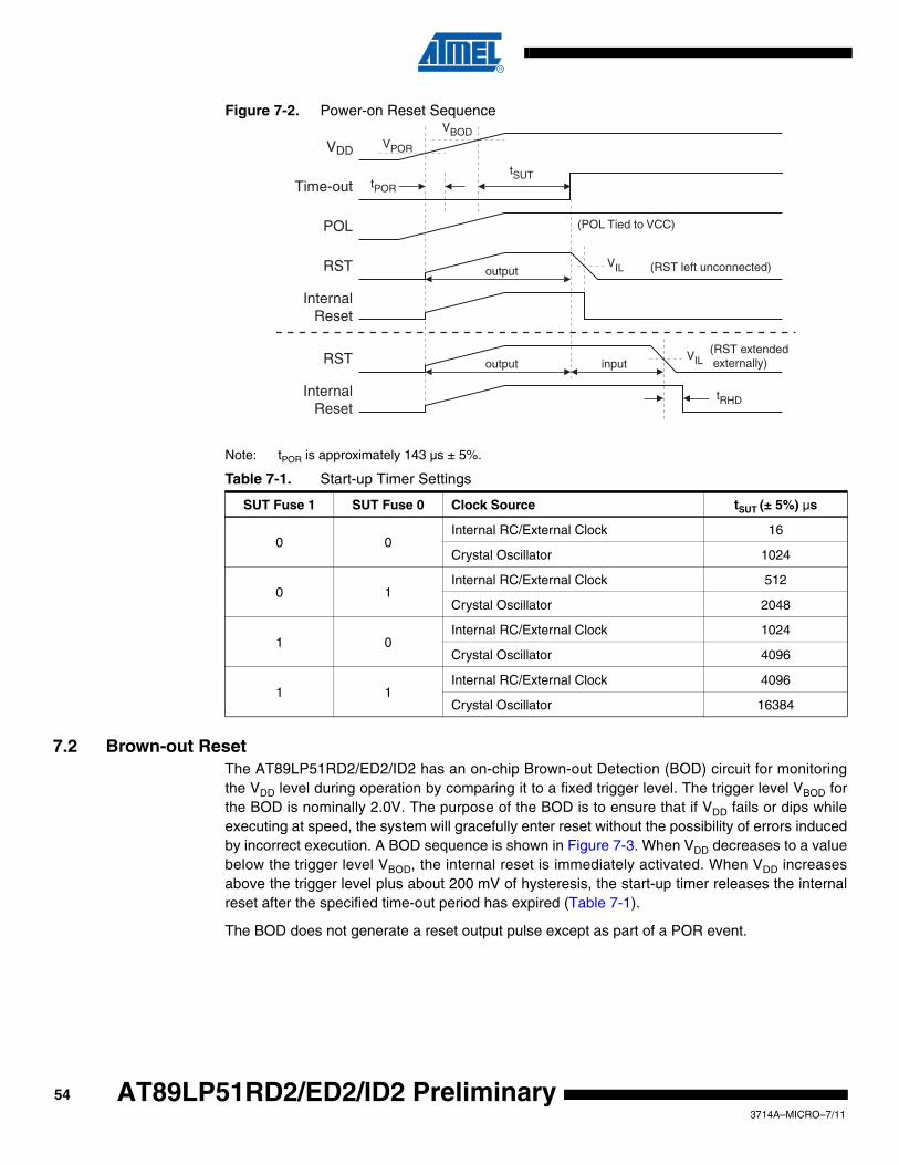
Figure 7-2. Power-on Reset Sequence
Note: tPOR is approximately 143 µs ± 5%.
7.2 Brown-out ResetThe AT89LP51RD2/ED2/ID2 has an on-chip Brown-out Detection (BOD) circuit for monitoringthe VDD level during operation by comparing it to a fixed trigger level. The trigger level VBOD forthe BOD is nominally 2.0V. The purpose of the BOD is to ensure that if VDD fails or dips whileexecuting at speed, the system will gracefully enter reset without the possibility of errors inducedby incorrect execution. A BOD sequence is shown in Figure 7-3. When VDD decreases to a valuebelow the trigger level VBOD, the internal reset is immediately activated. When VDD increasesabove the trigger level plus about 200 mV of hysteresis, the start-up timer releases the internalreset after the specified time-out period has expired (Table 7-1).
The BOD does not generate a reset output pulse except as part of a POR event.
Table 7-1. Start-up Timer Settings
SUT Fuse 1 SUT Fuse 0 Clock Source tSUT (± 5%) µs
0 0Internal RC/External Clock 16
Crystal Oscillator 1024
0 1Internal RC/External Clock 512
Crystal Oscillator 2048
1 0Internal RC/External Clock 1024
Crystal Oscillator 4096
1 1Internal RC/External Clock 4096
Crystal Oscillator 16384
VDD
RST
Time-out tPOR
tRHD
VPOR
InternalReset
RST
InternalReset
VIL
tSUT
VBOD
(RST left unconnected)
(RST extended externally)
POL (POL Tied to VCC)
VILoutput
output input
543714A–MICRO–7/11
AT89LP51RD2/ED2/ID2 Preliminary

AT89LP51RD2/ED2/ID2 Preliminary
Figure 7-3. Brown-out Detector Reset
The AT89LP51RD2/ED2/ID2 allows for a wide VDD operating range. The on-chip BOD may notbe sufficient to prevent incorrect execution if VBOD is lower than the minimum required VDD
range, such as when a 5.0V supply is coupled with high frequency operation. In such cases anexternal Brown-out Reset circuit connected to the RST pin may be required.
7.3 External ResetThe RST pin of the AT89LP51RD2/ED2/ID2 can function as either an active-low reset input oras an active-high reset input. The polarity of the RST pin is selectable using the POL pin (for-merly EA). When POL is high the RST pin is active high with an on-chip pull-down resistor tied toGND. When POL is low the RST pin is active low with an on-chip pull-up resistor tied to VDD. TheRST pin structure is shown in Figure 7-4. Entry into reset is completely asynchronous. The pres-ence of the active reset level on the input will immediately reset the device. A glitch filter willsuppress all reset input pulses of less than 50 ns. Exit from reset is synchronous. In Compatibil-ity mode the reset pin is sampled every six clock cycles and must be held inactive for at leasttwelve clock cycles to deassert the internal reset. In Fast mode the reset pin is sampled everyclock cycle and must be held inactive for at least two clock cycles to deassert the internal reset.
The AT89LP51RD2/ED2/ID2 includes an on-chip Power-On Reset and Brown-out Detector cir-cuit that ensures that the device is reset from system power up. In most cases a RC startupcircuit is not required on the RST pin, reducing system cost, and the RST pin may be left uncon-nected if a board-level reset is not present.
Note: RST also serves as the In-System Programming (ISP) enable. ISP is enabled when the external reset pin is held active. When ISP is disabled by fuse, ISP may only be entered by pulling RST active during power-up. If this behavior is necessary, it is recommended to use an active-low reset so that ISP can be entered by shorting RST to GND at power-up.
Figure 7-4. Reset Pin Structure
VDD
Time-out
VPOR
InternalReset
tSUT
VBOD
VCC
DISRTO
WDT Reset
RSTInternal Reset
POL = 1 VCC
DISRTO
WDT Reset
RSTInternal Reset
POL = 0
553714A–MICRO–7/11

7.4 Hardware Watchdog ResetWhen the Hardware Watchdog times out, it will generate a reset pulse lasting 49 clock cycles.By default this pulse is also output on the RST pin. The output pulse is either open-drain oropen-source as shown in Figure 7-4. In order to properly propagate this pulse to the rest of theboard in the case of an external capacitor or power-supply supervisor circuit, a 1 kΩ resistorshould be placed in series with any external driving circuitry as shown in Figure 7-5. To disablethe RST output the DISRTO bit in the WDTPRG register must be set to one. Watchdog reset willset the WDTOVF flag in WDTPRG. To prevent a Watchdog reset, the watchdog reset sequence1EH/E1H must be written to WDTRST before the Watchdog times out. See Section 16. on page106 for details on the operation of the Watchdog.
Figure 7-5. Recommended Reset Output Schematics
7.5 PCA Watchdog ResetModule 4 of the Programmable Counter Array (PCA) can be configured as a watchdog timer.When a compare match occurs between module 4 and the PCA timer, it will generate an internalreset pulse lasting 16 clock cycles. This pulse is never output on the RST pin. See Section 15.7on page 106 for details on the operation of the PCA Watchdog.
7.6 Software ResetThe CPU may generate a 49-clock cycle reset pulse by writing the software reset sequence5AH/A5H to the WDRST register. A software reset will set the SWRST bit in WDTPRG. See“Software Reset” on page 107 for more information on software reset. Writing any sequencesother than 5AH/A5H or 1EH/E1H to WDTRST will generate an immediate reset and set bothWDTOVF and SWRST to flag an error. Software reset will also drive the RST pin active unlessDISRTO is set.
RST
POL = 1
AT89LP51xD2
To otheron-boardcircuitry
1 kΩ
Vcc+
RST
Vcc RST
POL = 0
AT89LP51xD2
To otheron-boardcircuitry
1 kΩ
+
RST
Vcc
563714A–MICRO–7/11
AT89LP51RD2/ED2/ID2 Preliminary

AT89LP51RD2/ED2/ID2 Preliminary
8. Power Saving ModesThe AT89LP51RD2/ED2/ID2 supports two different software selectable power-reducing modes:Idle and Power-down. These modes are accessed through the PCON register. Additional stepsmay be required to achieve the lowest possible power consumption while using these modes. Inaddition the AT89LP51RD2/ED2/ID2 has fusible configuration options that can further reducethe active power consumption under certain circumstances.
8.1 Idle ModeSetting the IDL bit in PCON enters idle mode. Idle mode halts the internal CPU clock. The CPUstate is preserved in its entirety, including the RAM, stack pointer, program counter, programstatus word, and accumulator. The Port pins hold the logic states they had at the time that Idlewas activated. Idle mode leaves the peripherals running in order to allow them to wake up theCPU when an interrupt is generated. The timer and UART peripherals continue to function dur-ing Idle. If these functions are not needed during idle, they should be explicitly disabled byclearing the appropriate control bits in their respective SFRs. The watchdog may be selectivelyenabled or disabled during Idle by setting/clearing the WDIDLE bit. The Brown-out Detector isalways active during Idle. Any enabled interrupt source or reset may terminate Idle mode. Whenexiting Idle mode with an interrupt, the interrupt will immediately be serviced, and following RETIthe next instruction to be executed will be the one following the instruction that put the deviceinto Idle.
The power consumption during Idle mode can be further reduced by prescaling down the systemclock using the System Clock Prescaler (Section 6.8 on page 49). Be aware that the clockdivider will affect all peripheral functions and baud rates may need to be adjusted to maintaintheir rate with the new clock frequency..
Table 8-1. PCON – Power Control Register
PCON = 87H Reset Value = 000X 0000B
Not Bit Addressable
SMOD1 SMOD0 PWDEX POF GF1 GF0 PD IDL
Bit 7 6 5 4 3 2 1 0
Symbol Function
SMOD1 Double Baud Rate bit. Doubles the baud rate of the UART in Modes 1, 2, or 3.
SMOD0 Frame Error Select. When SMOD0 = 1, SCON.7 is SM0. When SMOD0 = 1, SCON.7 is FE. Note that FE will be set after a frame error regardless of the state of SMOD0.
PWDEX Power-down Exit Mode. When PWDEX = 0, wake up from Power-down is externally controlled. When PWDEX = 1, wake up from Power-down is internally timed.
POF Power Off Flag. POF is set to “1” during power up (i.e. cold reset). It can be set or reset under software control and is not affected by RST or BOD (i.e. warm resets).
GF1, GF0 General-purpose Flags
PD Power-down bit. Setting this bit activates power-down operation. The PD bit is cleared automatically by hardware when waking up from power-down.
IDL Idle Mode bit. Setting this bit activates Idle mode operation. The IDL bit is cleared automatically by hardware when waking up from idle
573714A–MICRO–7/11

8.2 Power-down ModeSetting the Power-down (PD) bit in PCON enters Power-down mode. Power-down mode stopsthe oscillator, disables the BOD and powers down the Flash memory in order to minimize powerconsumption. Only the power-on circuitry will continue to draw power during Power-down. Dur-ing Power-down, the power supply voltage may be reduced to the RAM keep-alive voltage. TheRAM contents will be retained, but the SFR contents are not guaranteed once VDD has beenreduced. Power-down may be exited by external reset, power-on reset, or certain enabledinterrupts.
8.2.1 Interrupt Recovery from Power-down Two external interrupt sources may be configured to terminate Power-down mode: externalinterrupts INT0 (P3.2) and INT1 (P3.3). To wake up by external interrupt INT0 or INT1, that inter-rupt must be enabled by setting EX0 or EX1 in IE and must be configured for level-sensitiveoperation by clearing IT0 or IT1.
When terminating Power-down by an interrupt, two different wake-up modes are available.When PWDEX in PCON is one, the wake-up period is internally timed as shown in Figure 8-1. Atthe falling edge on the interrupt pin, Power-down is exited, the oscillator is restarted, and aninternal timer begins counting. The internal clock will not be allowed to propagate to the CPUuntil after the timer has timed out. After the time-out period the interrupt service routine willbegin. The time-out period is controlled by the Start-up Timer Fuses (see Table 7-1 on page 54).The interrupt pin need not remain low for the entire time-out period.
Figure 8-1. Interrupt Recovery from Power-down (PWDEX = 1)
When PWDEX = “0”, the wake-up period is controlled externally by the interrupt. Again, at thefalling edge on the interrupt pin, power-down is exited and the oscillator is restarted. However,the internal clock will not propagate until the rising edge of the interrupt pin as shown in Figure 8-2. The interrupt pin should be held low long enough for the selected clock source to stabilize.After the rising edge on the pin the interrupt service routine will be executed.
PWD
INT1
XTAL1
tSUT
InternalClock
583714A–MICRO–7/11
AT89LP51RD2/ED2/ID2 Preliminary

AT89LP51RD2/ED2/ID2 Preliminary
Figure 8-2. Interrupt Recovery from Power-down (PWDEX = 0)
8.2.2 Reset Recovery from Power-downThe wake-up from Power-down through an external reset is similar to the interrupt withPWDEX = “1”. At the rising edge of RST, Power-down is exited, the oscillator is restarted, andan internal timer begins counting as shown in Figure 8-3. The internal clock will not be allowed topropagate to the CPU until after the timer has timed out. The time-out period is controlled by theStart-up Timer Fuses. (See Table 7-1 on page 54). If RST returns low before the time-out, a twoclock cycle internal reset is generated when the internal clock restarts. Otherwise, the device willremain in reset until RST is brought low.
Figure 8-3. Reset Recovery from Power-down (POL = 1)
8.3 Reducing Power ConsumptionSeveral possibilities need consideration when trying to reduce the power consumption in an8051-based system.
• Idle or Power-down mode should be used as often as possible with interrupts waking up the system to handle specific tasks
• All un-needed peripheral functions should be disabled
• The System Clock Prescaler can scale down the operating frequency during periods of low demand (See “System Clock Prescaler” on page 49.)
• The ALE output can be disabled by setting AO in AUXR, thereby also reducing EMI
• Write to the EEPROM by page instead of by byte to limit the number of write cycles
• For AT89LP51ID2, switch the system clock from a high power oscillator like XTALA to a lower power oscillator like the internal 8 MHz oscillator during periods when frequency accuracy is not as important.
PWD
INT1
XTAL1
InternalClock
PWD
RST
XTAL1
tSUT
Internal Clock
Internal Reset
593714A–MICRO–7/11

8.4 Low Power ConfigurationSeveral of the nonvolatile User Configuration Fuses can enable modes where less power will beconsumed during normal operation as listed in Table 8-2. These fuses must generally be setonce by an external programmer to match the desired operating environment.
• For crystal frequencies of 12 MHz or less, OSCA should be placed in Low Power Crystal Oscillator mode
• X1 Mode is supported for compatibility with existing applications. X2 Mode should be used to achieve the same CPU and peripheral speed at half the crystal frequency
• The Low Power Mode settings change the slope and intercept of the active current versus frequency relationship. See Table 8-3 below.
Table 8-2. User Configuration Fuses Affecting Power Consumption
Fuse Name Description
Clock Source AThe Low Power Crystal Oscillator (setting 2) will use half the power of the High Speed Crystal Oscillator (setting 3) for the same frequency ( ≤ 12 MHz)
X2 ModeX2 mode can keep the same CPU speed while cutting the crystal frequency in half.
Low Power Mode
Low Power Mode can reduce the power consumption for system frequencies under 20 MHz. Extra Low Power Mode can further reduce the power if the system frequency is less than 1 MHz.
Table 8-3. Low Power Mode Fuses
Fuse 1 (0EH)
Fuse 0 (0DH) Mode Description
00H (0) FFH (1)Extra Low Power
Lowest power mode. Use only if the oscillator frequency can never be above 1 MHz.
FFH (1) FFH (0) Low Power
Low power mode will reduce consumption for CPU frequencies under 10 MHz and slightly increase consumption for CPU frequencies over 10 MHz compared to Normal Mode. This mode is best for oscillator frequencies below 10 MHz or for frequencies 10–20 MHz where the prescaler may be used to scale the CPU frequency below 10 MHz.
— 00H (0) Normal
Normal mode has higher consumption than Low Power mode for CPU frequencies under 10 MHz but slightly less consumption for CPU frequencies over 10 MHz. This mode is best for oscillator frequencies over 20 MHz or for frequencies 10–20 MHz where the prescaler is not used to scale the CPU frequency.
603714A–MICRO–7/11
AT89LP51RD2/ED2/ID2 Preliminary

AT89LP51RD2/ED2/ID2 Preliminary
9. InterruptsThe AT89LP51RD2/ED2/ID2 provides 11 interrupt vectors: two external interrupts (INT0 andINT1), three timer interrupts (Timers 0, 1 and 2), a serial port interrupt, an SPI interrupt, a key-board interrupt, a PCA interrupt, an analog comparator interrupt and an ADC interrupt. Theseinterrupts and the system reset each have a separate program vector at the start of the programmemory space.
Each interrupt source can be individually enabled or disabled by setting or clearing a bit in theinterrupt enable registers: IEN0 and IEN1. The IEN0 register also contains a global disable bit,EA, which disables all interrupts. All of the bits that generate interrupts can be set or cleared bysoftware, with the same result as though they had been set or cleared by hardware. That is,interrupts can be generated and pending interrupts can be canceled in software.
9.1 Interrupt PriorityEach interrupt source can be individually programmed to one of four priority levels by setting orclearing bits in the interrupt priority registers: IPL0, IPL1, IPH0 and IPH1. IPL0 and IPL1 hold thelow order priority bits and IPH0 and IPH1 hold the high priority bits for each interrupt as shown inTable 9-2. An interrupt service routine in progress can be interrupted by a higher priority inter-rupt, but not by another interrupt of the same or lower priority. The highest priority interruptcannot be interrupted by any other interrupt source. If two requests of different priority levels arepending at the end of an instruction, the request of higher priority level is serviced. If requests ofthe same priority level are pending at the end of an instruction, an internal polling sequencedetermines which request is serviced. The polling sequence is based on the vector address; aninterrupt with a lower vector address has higher priority than an interrupt with a higher vectoraddress, except in the case of the PCA, whose polling priority is moved up by two as shown inTable 9-1 and Figure 9-1. Note that the polling sequence is only used to resolve pendingrequests of the same priority level.
Table 9-1. Interrupt Vector Addresses and Priority
Polling Priority Interrupt Source
Vector Address
0 System Reset RST or POR or BOD 0000H
1 External Interrupt 0 IE0 0003H
2 Timer 0 Overflow TF0 000BH
3 External Interrupt 1 IE1 0013H
4 Timer 1 Overflow TF1 001BH
6 Serial Port Interrupt RI or TI 0023H
7 Timer 2 Interrupt TF2 or EXF2 002BH
5 PCA Interrupt CF, CCF0, CCF1, CCF2, CCF3 or CCF4 0033H
8 Keyboard Interrupt KBF7-0 003BH
9 Two-Wire Interrupt SI 0043H
10 SPI Interrupt SPIF or MODF or TXE 004BH
11 reserved 0053H
12 Analog Comparator Interrupt CFA or CFB 005BH
13 ADC Interrupt ADIF 0063H
613714A–MICRO–7/11
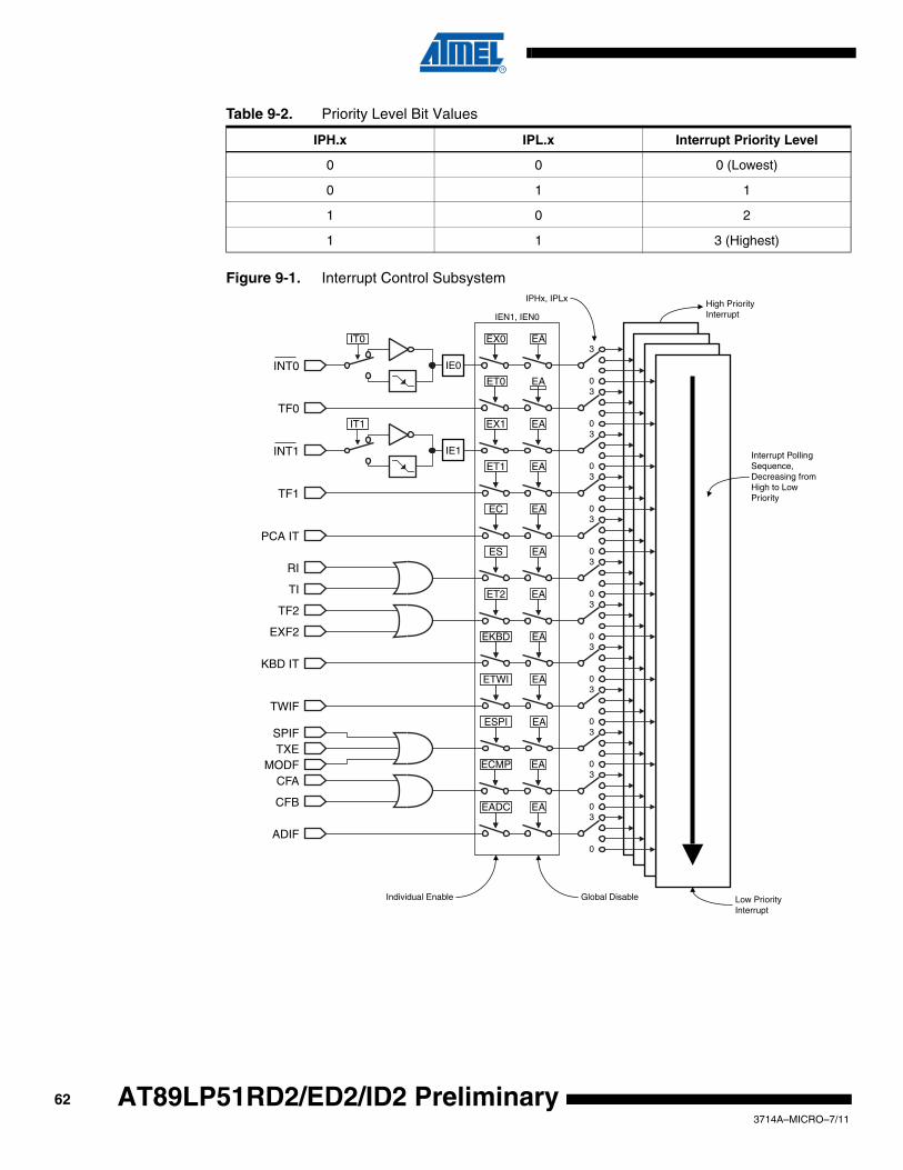
Figure 9-1. Interrupt Control Subsystem
Table 9-2. Priority Level Bit Values
IPH.x IPL.x Interrupt Priority Level
0 0 0 (Lowest)
0 1 1
1 0 2
1 1 3 (Highest)
TF0
EA
INT0
IPHx, IPLx
IEN1, IEN0
EA
EA
EA
EA
EA
EA
EA
IT0
IE0
INT1
IT1
IE1
TF1
PCA IT
RI
TI
TF2
EXF2
KBD ITEA
EATWIF
SPIF
MODFTXE
EA
EA
CFA
CFB
ADIF
EX0
ET0
EX1
ET1
EC
ES
ET2
EKBD
ETWI
ESPI
ECMP
EADC
3
03
03
03
03
03
03
03
03
03
03
03
0
High PriorityInterrupt
Low PriorityInterrupt
Global DisableIndividual Enable
Interrupt PollingSequence, Decreasing fromHigh to LowPriority
623714A–MICRO–7/11
AT89LP51RD2/ED2/ID2 Preliminary
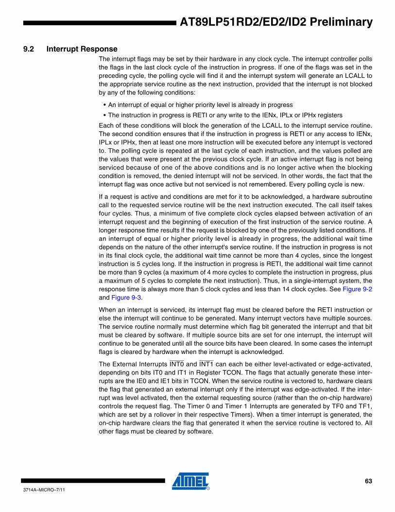
AT89LP51RD2/ED2/ID2 Preliminary
9.2 Interrupt ResponseThe interrupt flags may be set by their hardware in any clock cycle. The interrupt controller pollsthe flags in the last clock cycle of the instruction in progress. If one of the flags was set in thepreceding cycle, the polling cycle will find it and the interrupt system will generate an LCALL tothe appropriate service routine as the next instruction, provided that the interrupt is not blockedby any of the following conditions:
• An interrupt of equal or higher priority level is already in progress
• The instruction in progress is RETI or any write to the IENx, IPLx or IPHx registers
Each of these conditions will block the generation of the LCALL to the interrupt service routine.The second condition ensures that if the instruction in progress is RETI or any access to IENx,IPLx or IPHx, then at least one more instruction will be executed before any interrupt is vectoredto. The polling cycle is repeated at the last cycle of each instruction, and the values polled arethe values that were present at the previous clock cycle. If an active interrupt flag is not beingserviced because of one of the above conditions and is no longer active when the blockingcondition is removed, the denied interrupt will not be serviced. In other words, the fact that theinterrupt flag was once active but not serviced is not remembered. Every polling cycle is new.
If a request is active and conditions are met for it to be acknowledged, a hardware subroutinecall to the requested service routine will be the next instruction executed. The call itself takesfour cycles. Thus, a minimum of five complete clock cycles elapsed between activation of aninterrupt request and the beginning of execution of the first instruction of the service routine. Alonger response time results if the request is blocked by one of the previously listed conditions. Ifan interrupt of equal or higher priority level is already in progress, the additional wait timedepends on the nature of the other interrupt's service routine. If the instruction in progress is notin its final clock cycle, the additional wait time cannot be more than 4 cycles, since the longestinstruction is 5 cycles long. If the instruction in progress is RETI, the additional wait time cannotbe more than 9 cycles (a maximum of 4 more cycles to complete the instruction in progress, plusa maximum of 5 cycles to complete the next instruction). Thus, in a single-interrupt system, theresponse time is always more than 5 clock cycles and less than 14 clock cycles. See Figure 9-2and Figure 9-3.
When an interrupt is serviced, its interrupt flag must be cleared before the RETI instruction orelse the interrupt will continue to be generated. Many interrupt vectors have multiple sources.The service routine normally must determine which flag bit generated the interrupt and that bitmust be cleared by software. If multiple source bits are set for one interrupt, the interrupt willcontinue to be generated until all the source bits have been cleared. In some cases the interruptflags is cleared by hardware when the interrupt is acknowledged.
The External Interrupts INT0 and INT1 can each be either level-activated or edge-activated,depending on bits IT0 and IT1 in Register TCON. The flags that actually generate these inter-rupts are the IE0 and IE1 bits in TCON. When the service routine is vectored to, hardware clearsthe flag that generated an external interrupt only if the interrupt was edge-activated. If the inter-rupt was level activated, then the external requesting source (rather than the on-chip hardware)controls the request flag. The Timer 0 and Timer 1 Interrupts are generated by TF0 and TF1,which are set by a rollover in their respective Timers). When a timer interrupt is generated, theon-chip hardware clears the flag that generated it when the service routine is vectored to. Allother flags must be cleared by software.
633714A–MICRO–7/11
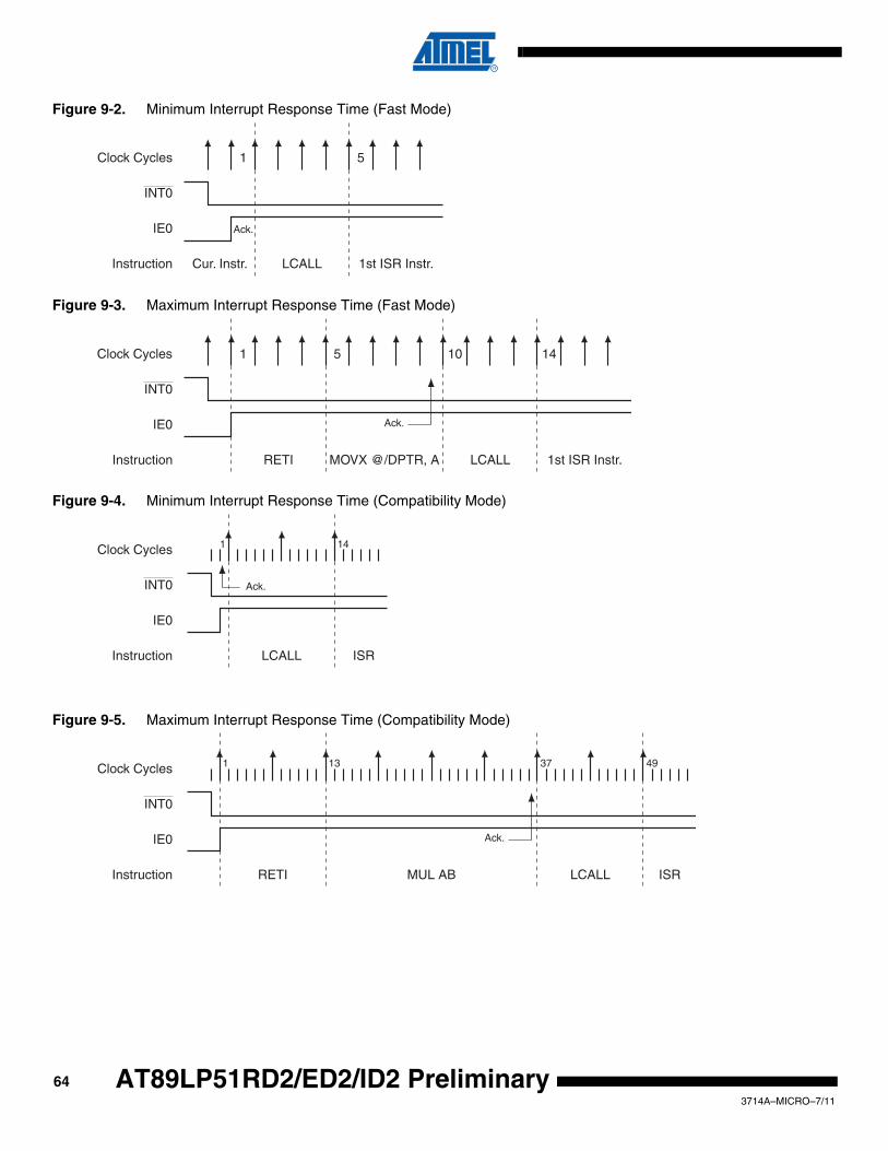
Figure 9-2. Minimum Interrupt Response Time (Fast Mode)
Figure 9-3. Maximum Interrupt Response Time (Fast Mode)
Figure 9-4. Minimum Interrupt Response Time (Compatibility Mode)
Figure 9-5. Maximum Interrupt Response Time (Compatibility Mode)
Clock Cycles
INT0
IE0
1 5
Instruction LCALL 1st ISR Instr.Cur. Instr.
Ack.
Clock Cycles
INT0
IE0
1 14
Instruction RETI MOVX @/DPTR, A LCALL 1st ISR Instr.
Ack.
5 10
Clock Cycles
INT0
IE0
1
Instruction LCALL ISR
Ack.
14
Clock Cycles
INT0
IE0
1
Instruction RETI MUL AB LCALL ISR
Ack.
13 37 49
643714A–MICRO–7/11
AT89LP51RD2/ED2/ID2 Preliminary

AT89LP51RD2/ED2/ID2 Preliminary
9.3 Interrupt RegistersTable 9-3. IEN0 – Interrupt Enable Register 0
IEN0 = A8H Reset Value = 0000 0000B
Bit Addressable
EA EC ET2 ES ET1 EX1 ET0 EX0
Bit 7 6 5 4 3 2 1 0
Symbol Function
EAGlobal Interrupt Enable
All interrupts are disabled when EA = 0. When EA = 1, each interrupt source is enabled/disabled by setting /clearing its own enable bit.
ECPCA Interrupt Enable
Clear to disable the PCA interrupt. Set to enable the PCA interrupt when EA = 1.
ET2Timer 2 Interrupt Enable
Clear to disable the Timer 2 interrupt. Set to enable the Timer 2 interrupt when EA = 1.
ESSerial Port Interrupt Enable
Clear to disable the UART interrupt. Set to enable the UART interrupt when EA = 1.
ET1Timer 1 Interrupt Enable
Clear to disable the Timer 1 interrupt. Set to enable the Timer 1 interrupt when EA = 1.
EX1External Interrupt 1 Enable.
Clear to disable the INT1 interrupt. Set to enable the INT1 interrupt when EA = 1.
ET0Timer 0 Interrupt Enable
Clear to disable the Timer 0 interrupt. Set to enable the Timer 0 interrupt when EA = 1.
EX0External Interrupt 0 Enable
Clear to disable the INT0 interrupt. Set to enable the INT0 interrupt when EA = 1.
Table 9-4. IEN1 – Interrupt Enable Register 1
IEN1 = B1H Reset Value = 0000 0000B
Bit Addressable
– – EADC ECMP – ESPI ETWI EKBD
Bit 7 6 5 4 3 2 1 0
Symbol Function
EADCADC Interrupt Enable.
Clear to disable the ADC interrupt. Set to enable the ADC interrupt when EA = 1.
ECMPAnalog COmparator Interrupt Enable
Clear to disable the Analog Comparator interrupt. Set to enable the Analog Comparator interrupt when EA = 1.
ESPISPI Interrupt Enable
Clear to disable the SPI interrupt. Set to enable the SPI interrupt when EA = 1.
ETWITWI Interrupt Enable
Clear to disable the TWI interrupt. Set to enable the TWI interrupt when EA = 1.
EKBDKeyboard Interrupt Enable
Clear to disable the Keyboard interrupt. Set to enable the Keyboard interrupt when EA = 1.
653714A–MICRO–7/11

Table 9-5. IPL0 – Interrupt Priority Low Register 0
IPL0 = B8H Reset Value = 0000 0000B
Bit Addressable
IP0DIS PPCL PT2L PSL PT1L PX1L PT0L PX0L
Bit 7 6 5 4 3 2 1 0
Symbol Function
IP0DISInterrupt Level 0 Disable
Clear to enable all interrupts with priority level 0. Set to disable all interrupts with priority level 0.
PPCLPCA Interrupt Priority Low
Low order bit for PCA interrupt priority level.
PT2LTimer 2 Interrupt Priority Low
Low order bit for Timer 2 interrupt priority level.
PSLSerial Port Interrupt Priority Low
Low order bit for UART interrupt priority level.
PT1LTimer 1 Interrupt Priority Low
Low order bit for Timer 1 interrupt priority level.
PX1LExternal Interrupt 1 Priority Low
Low order bit for INT1 interrupt priority level.
PT0LTimer 0 Interrupt Priority Low
Low order bit for Timer 0 interrupt priority level.
PX0LExternal Interrupt 0 Priority Low
Low order bit for INT0 interrupt priority level.
Table 9-6. IPL1 – Interrupt Priority Low Register 1
IPL1 = B2H Reset Value = 0000 0000B
Bit Addressable
IP2DIS – PADCL PCMPL – PSPL PTWL PKBL
Bit 7 6 5 4 3 2 1 0
Symbol Function
IP2DISInterrupt Level 2 Disable
Clear to enable all interrupts with priority level 2. Set to disable all interrupts with priority level 2.
PADCLADC Interrupt Priority Low
Low order bit for ADC interrupt priority level.
PCMPLAnalog Comparator Interrupt Priority Low
Low order bit for Analog Comparator interrupt priority level.
PSPLSPI Interrupt Priority Low
Low order bit for SPI interrupt priority level.
PTWLTWI Interrupt Priority Low
Low order bit for TWI interrupt priority level.
PKBLKeyboard Interrupt Priority Low
Low order bit for Keyboard interrupt priority level.
663714A–MICRO–7/11
AT89LP51RD2/ED2/ID2 Preliminary

AT89LP51RD2/ED2/ID2 Preliminary
Table 9-7. IPH0 – Interrupt Priority High Register 0
IPH0 = B7H Reset Value = 0000 0000B
Not Bit Addressable
IP1DIS PPCH PT2H PSH PT1H PX1H PT0H PX0H
Bit 7 6 5 4 3 2 1 0
Symbol Function
IP1DISInterrupt Level 1 Disable
Clear to enable all interrupts with priority level 1. Set to disable all interrupts with priority level 1.
PPCHPCA Interrupt Priority High
High order bit for PCA interrupt priority level.
PT2HTimer 2 Interrupt Priority High
High order bit for Timer 2 interrupt priority level.
PSHSerial Port Interrupt Priority High
High order bit for UART interrupt priority level.
PT1HTimer 1 Interrupt Priority High
High order bit for Timer 1 interrupt priority level.
PX1HExternal Interrupt 1 Priority High
High order bit for INT1 interrupt priority level.
PT0HTimer 0 Interrupt Priority High
High order bit for Timer 0 interrupt priority level.
PX0HExternal Interrupt 0 Priority High
High order bit for INT0 interrupt priority level.
Table 9-8. IPH1 – Interrupt Priority High Register 1
IPH1 = B3H Reset Value = 0000 0000B
Not Bit Addressable
IP3DIS – PADCH PCMPH – PSPH PTWH PKBH
Bit 7 6 5 4 3 2 1 0
Symbol Function
IP3DISInterrupt Level 3 Disable
Clear to enable all interrupts with priority level 3. Set to disable all interrupts with priority level 3.
PADCHADC Interrupt Priority High
High order bit for ADC interrupt priority level.
PCMPHAnalog Comparator Interrupt Priority High
High order bit for Analog Comparator interrupt priority level.
PSPHSPI Interrupt Priority High
High order bit for SPI interrupt priority level.
PTWHTWI Interrupt Priority High
High order bit for TWI interrupt priority level.
PKBHKeyboard Interrupt Priority High
High order bit for Keyboard interrupt priority level.
673714A–MICRO–7/11

10. External InterruptsThe INT0 (P3.2) and INT1 (P3.3) pins of the AT89LP51RD2/ED2/ID2 may be used as externalinterrupt sources. The external interrupts can be programmed to be level-activated or transition-activated by setting or clearing bit IT1 or IT0 in Register TCON. If ITx = 0, external interrupt x istriggered by a detected low at the INTx pin. If ITx = 1, external interrupt x is edge-triggered. Inthis mode if successive samples of the INTx pin show a high in one cycle and a low in the nextcycle, interrupt request flag IEx in TCON is set. Flag bit IEx then requests the interrupt.
Since the external interrupt pins are sampled once each clock cycle, an input high or low shouldhold for at least 2 system periods to ensure sampling. If the external interrupt is transition-acti-vated, the external source has to hold the request pin high for at least two clock cycles, and thenhold it low for at least two clock cycles to ensure that the transition is seen so that interruptrequest flag IEx will be set. IEx will be automatically cleared by the CPU when the service rou-tine is called if generated in edge-triggered mode. If the external interrupt is level-activated, theexternal source has to hold the request active until the requested interrupt is actually generated.Then the external source must deactivate the request before the interrupt service routine is com-pleted, or else another interrupt will be generated. Both INT0 and INT1 may wake up the devicefrom the Power-down state.
Other peripheral pins can also generate interrupts in response to an external event:
• A negative edge on the T2EX pin (P1.1) can set the EXF2 flag in T2CON
• Transitions on the PCA capture inputs CEX0–CEX4 (P1.3–7) can set the CCFx bits in CCON
• Transitions or levels on Port 1 can set the bits in KBF using the keyboard interface (see next section).
11. Keyboard Interface and General-purpose InterruptsThe AT89LP51RD2/ED2/ID2 implements a keyboard interface allowing the connection of a 1 x nto 8 x n matrix keyboard. The keyboard function provides 8 configurable external interrupts onPort 1. Each port pin can detect high/low levels or positive/negative edges. The keyboard inputsare considered as 8 independent interrupt sources sharing the same interrupt vector. The KBEregister selects which bits of Port 1 are enabled to generate an interrupt. The KBMOD and KBLSregisters determine the mode for each individual pin. KBMOD selects between level-sensitiveand edge-triggered mode. KBLS selects between high/low in level mode and positive/negative inedge mode. A block diagram is shown in Figure 11-1.
The pins of Port 1 are sampled every clock cycle. In level-sensitive mode, a valid level mustappear in two successive samples before generating the interrupt. In edge-triggered mode, atransition will be detected if the value changes from one sample to the next. When an interruptcondition on a pin is detected, and that pin is enabled, the appropriate flag in the KBF register isset. The flags in KBF must be cleared by software. Any enabled keyboard interrupt may wake upthe device from the Idle or Power-down state.
Unlike AT89C51RD2/ED2/ID2 the flags in KBF are not cleared by reading the register. The soft-ware may clear each bit individually or all at once. This allows the interface to be used forgeneral purpose external interrupts where some flags can be left pending between calls to theservice routine. Each flag can also be made pending by software by writing a one to it. Toachieve the same behavior as AT89C51RD2/ED2/ID2, the service routine must clear the entireregister.
683714A–MICRO–7/11
AT89LP51RD2/ED2/ID2 Preliminary

AT89LP51RD2/ED2/ID2 Preliminary
Figure 11-1. Keyboard Block Diagram
D Q
2 2 2 2
0 0
1 1
(P1.2) GPI2
D Q
1 1 1 1
0 0
1 1
(P1.1) GPI1
D Q
0 0 0 0
0 0
1 1
(P1.0) GPI0
D Q
3 3 3 3
0 0
1 1
(P1.3) GPI3
D Q
6 6 6 6
0 0
1 1
(P1.6) GPI6
D Q
5 5 5 5
0 0
1 1
(P1.5) GPI5
D Q
4 4 4 4
0 0
1 1
(P1.4) GPI4
D Q
7 7 7 7
0 0
1 1
(P1.7) GPI7
KBMODKBLS KBE KBF
Interrupt
CLK
693714A–MICRO–7/11
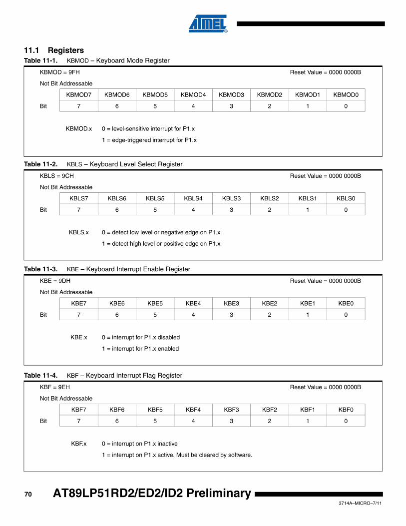
11.1 Registers.
.
.
Table 11-1. KBMOD – Keyboard Mode Register
KBMOD = 9FH Reset Value = 0000 0000B
Not Bit Addressable
KBMOD7 KBMOD6 KBMOD5 KBMOD4 KBMOD3 KBMOD2 KBMOD1 KBMOD0
Bit 7 6 5 4 3 2 1 0
KBMOD.x 0 = level-sensitive interrupt for P1.x
1 = edge-triggered interrupt for P1.x
Table 11-2. KBLS – Keyboard Level Select Register
KBLS = 9CH Reset Value = 0000 0000B
Not Bit Addressable
KBLS7 KBLS6 KBLS5 KBLS4 KBLS3 KBLS2 KBLS1 KBLS0
Bit 7 6 5 4 3 2 1 0
KBLS.x 0 = detect low level or negative edge on P1.x
1 = detect high level or positive edge on P1.x
Table 11-3. KBE – Keyboard Interrupt Enable Register
KBE = 9DH Reset Value = 0000 0000B
Not Bit Addressable
KBE7 KBE6 KBE5 KBE4 KBE3 KBE2 KBE1 KBE0
Bit 7 6 5 4 3 2 1 0
KBE.x 0 = interrupt for P1.x disabled
1 = interrupt for P1.x enabled
Table 11-4. KBF – Keyboard Interrupt Flag Register
KBF = 9EH Reset Value = 0000 0000B
Not Bit Addressable
KBF7 KBF6 KBF5 KBF4 KBF3 KBF2 KBF1 KBF0
Bit 7 6 5 4 3 2 1 0
KBF.x 0 = interrupt on P1.x inactive
1 = interrupt on P1.x active. Must be cleared by software.
703714A–MICRO–7/11
AT89LP51RD2/ED2/ID2 Preliminary

AT89LP51RD2/ED2/ID2 Preliminary
12. I/O PortsThe AT89LP51RD2/ED2/ID2 can be configured for between 36 and 40 I/O pins. The exact num-ber of general I/O pins available depends on the clock and external memory configuration asshown in Table 12-1.
Note: On AT89LP51ID2 OSCB requires 0, 1 or 2 I/O pins depending on the Clock Source B setting. Dis-abling OSCB (OscbEn = 0) frees up the OSCB pins for general use. Disabling OSCA (OscAEn = 0) does NOT free up the OSCA pins. OSCA must be configured for Internal RC mode to use these pins even when running from OSCB only.
12.1 Port ConfigurationAll port pins on the AT89LP51RD2/ED2/ID2 may be configured in one of four modes: quasi-bidi-rectional (standard 8051 port outputs), push-pull output, open-drain output, or input-only. Portmodes may be assigned in software on a pin-by-pin basis as shown in Table 12-2 using the reg-isters listed in Table 12-3. The Tristate-Port User Fuse (See Section 24.2 on page 190)determines the default state of the port pins. When the fuse is enabled, all port pins on P1, P2and P3 default to input-only mode after reset. When the fuse is disabled, all port pins on P1, P2and P3 default to quasi-bidirectional mode after reset and are weakly pulled high. P0 alwaysdefaults to open-drain mode. P4.4–5 always default to quasi-bidirectional mode. P4.0–1 alwaysdefault to open-drain. The other pins of P4 obey the fuse.
Each port pin also has a Schmitt-triggered input for improved input noise rejection. DuringPower-down all the Schmitt-triggered inputs are disabled with the exception of P3.2 (INT0), P3.3(INT1), RST, P4.6 (XTAL1) and P4.7 (XTAL2). Therefore, P3.2, P3.3, P4.6 and P4.7 should notbe left floating during Power-down. n addition any pin of Port 1 configured as a keyboard inter-rupt input will also remain active during Power-down to wake-up the device. These interrupt pinsshould either be disabled before entering Power-down or they should not be left floating.
Table 12-1. AT89LP51RD2/ED2 I/O Pin Configurations
Clock Source A External Program Access External Data AccessNumber of I/O
Pins
External Crystal or Resonator
Yes (PSEN+ALE+P0+P2)Yes (RD+WR) 18
No 20
No
8-bit (ALE+RD+WR+P0) 27
16-bit (ALE+RD+WR+P0) 19
No 38
External Clock
Yes (PSEN+ALE+P0+P2)Yes (RD+WR) 19
No 21
No
8-bit (ALE+RD+WR+P0) 28
16-bit (ALE+RD+WR+P0+P2) 20
No 39
Internal RC Oscillator
Yes (PSEN+ALE+P0+P2)Yes (RD+WR) 20
No 22
No
8-bit (ALE+RD+WR+P0) 29
16-bit (ALE+RD+WR+P0+P2) 21
No 40
713714A–MICRO–711

.
.
.
12.1.1 Quasi-bidirectional OutputPort pins in quasi-bidirectional output mode function similar to standard 8051 port pins. A Quasi-bidirectional port can be used both as an input and output without the need to reconfigure theport. This is possible because when the port outputs a logic high, it is weakly driven, allowing anexternal device to pull the pin low. When the pin is driven low, it is driven strongly and able tosink a large current. There are three pull-up transistors in the quasi-bidirectional output thatserve different purposes.
One of these pull-ups, called the “very weak” pull-up, is turned on whenever the port latch for thepin contains a logic “1”. This very weak pull-up sources a very small current that will pull the pinhigh if it is left floating. When the pin is pulled low externally this pull-up will always source somecurrent. The very weak pull-up is disabled when the port register contains a zero. In addition thevery weak pull-ups of all quasi-bidirectional ports can be disabled globally by setting the DPU bitin the AUXR register (See Table 3-3 on page 19).
Table 12-2. Configuration Modes for Port x Pin y
PxM0.y PxM1.y Port Mode
0 0 Quasi-bidirectional
0 1 Push-pull Output
1 0 Input Only (High Impedance)
1 1 Open-Drain Output
Table 12-3. Port Configuration Registers
Port Port Data Port Configuration
0 P0 (80H) P0M0 (D4H), P0M1 (D5H)
1 P1 (90H) P1M0 (E6H), P1M1 (E7H)
2 P2 (A0H) P2M0 (D6H), P2M1 (D7H)
3 P3 (B0H) P3M0 (DEH), P3M1 (CFH)
4 P4 (C0H) P4M0 (BEH), P4M1 (BFH)
Table 12-4. Port Configuration Reset Values
Register Tristate Ports Fuse = FFH (1) Tristate Ports Fuse = 00H (0)
P0M0 FF FF
P0M1 FF FF
P1M0 FF 00
P1M1 00 00
P2M0 FF 00
P2M1 00 00
P3M0 FF 00
P3M1 00 00
P4M0 C7 03
P4M0 03 03
723714A–MICRO–711
AT89LP51RD2/ED2/ID2 Preliminary

AT89LP51RD2/ED2/ID2 Preliminary
A second pull-up, called the “weak” pull-up, is turned on when the port latch for the pin containsa logic “1” and the pin itself is also at a logic “1” level. This pull-up provides the primary sourcecurrent for a quasi-bidirectional pin that is outputting a “1”. If this pin is pulled low by an externaldevice, this weak pull-up turns off, and only the very weak pull-up remains on. In order to pull thepin low under these conditions, the external device has to sink enough current to overpower theweak pull-up and pull the port pin below its input threshold voltage.
The third pull-up is referred to as the “strong” pull-up. This pull-up is used to speed up low-to-high transitions on a quasi-bidirectional port pin when the port latch changes from a logic “0” to alogic “1”. When this occurs, the strong pull-up turns on for one CPU clock, quickly pulling the portpin high. The quasi-bidirectional port configuration is shown in Figure 12-1.
12.1.2 Input-only ModeThe input only port configuration is shown in Figure 12-2. The output drivers are tristated. Theinput includes a Schmitt-triggered input for improved input noise rejection. The input circuitry ofP3.2, P3.3, P4.6 and P4.7 is not disabled during Power-down (see Figure 12-3) and thereforethese pins should not be left floating during Power-down when configured in this mode.
Input-only mode can reduce power consumption for low-level inputs over quasi-bidirectionalmode because the “very weak” pull-up is turned off and only very small leakage current in thesub microamp range is present.
Figure 12-1. Quasi-bidirectional Output
Figure 12-2. Input Only
Figure 12-3. Input Circuit for P3.2, P3.3, P4.6 and P4.7
1 Clo c k Del a y (D Flip-Flop) Strong V e r y
W ea k W ea k
P o r t Pin
V CC V CC V CC
F rom P o r t Register
Input Data
PWD
P o r t Pin
Input Data
PWD
PortPin
InputData
733714A–MICRO–711

12.1.3 Open-drain OutputThe open-drain output configuration turns off all pull-ups and only drives the pull-down transistorof the port pin when the port latch contains a logic “0”. To be used as a logic output, a port con-figured in this manner must have an external pull-up, typically a resistor tied to VDD. The pull-down for this mode is the same as for the quasi-bidirectional mode. The open-drain port configu-ration is shown in Figure 12-4. The input circuitry of P3.2, P3.3, P4.6 and P4.7 is not disabledduring Power-down (see Figure 12-3) and therefore these pins should not be left floating duringPower-down when configured in this mode.
Figure 12-4. Open-Drain Output
12.1.4 Push-pull OutputThe push-pull output configuration has the same pull-down structure as both the open-drain andthe quasi-bidirectional output modes, but provides a continuous strong pull-up when the portlatch contains a logic “1”. The push-pull mode may be used when more source current is neededfrom a port output. The push-pull port configuration is shown in Figure 12-5.
Figure 12-5. Push-pull Output
12.2 Port Analog FunctionsThe AT89LP51RD2/ED2/ID2 incorporates two analog comparators and an 8-channel analog-to-digital converter. In order to give the best analog performance and minimize power consump-tion, pins that are being used for analog functions must have both their digital outputs and digitalinputs disabled. Digital outputs are disabled by putting the port pins into the input-only mode asdescribed in “Port Configuration” on page 71. The analog input pins will always default to input-only mode after reset regardless of the state of the Tristate-Port Fuse.
P o r t Pin
F rom P o r t Register
Input Data
PWD
P o r t Pin
V CC
F rom P o r t Register
Input Data
PWD
743714A–MICRO–711
AT89LP51RD2/ED2/ID2 Preliminary

AT89LP51RD2/ED2/ID2 Preliminary
Digital inputs on P2.4, P2.5, P2.6 and P2.7 are disabled whenever an analog comparator isenabled by setting the CENA or CENB bits in ACSRA and ACSRB and that pin is configured forinput-only mode. To use an analog input pin as a high-impedance digital input while a compara-tor is enabled, that pin should be configured in open-drain mode and the corresponding portregister bit should be set to 1.
Digital inputs on Port 0 are disabled for each pin configured for input-only mode whenever theADC is enabled by setting the ADCE bit and clearing the DAC bit in DADC. To use any Port 0input pin as a high-impedance digital input while the ADC is enabled, that pin should be config-ured in open-drain mode and the corresponding port register bit should be set to 1. When DACmode is enabled, P2.2 and P2.3 are forced to input-only mode.
12.3 Port Read-Modify-Write A read from a port will read either the state of the pins or the state of the port register dependingon which instruction is used. Simple read instructions will always access the port pins directly.Read-modify-write instructions, which read a value, possibly modify it, and then write it back, willalways access the port register. This includes bit write instructions such as CLR or SETB as theyactually read the entire port, modify a single bit, then write the data back to the entire port. SeeTable 12-5 for a complete list of Read-Modify-Write instruction which may access the ports.
12.4 Port Alternate FunctionsMost general-purpose digital I/O pins of the AT89LP51RD2/ED2/ID2 share functionality with thevarious I/Os needed for the peripheral units. Table 12-7 lists the alternate functions of the portpins. Alternate functions are connected to the pins in a logic AND fashion. In order to enable thealternate function on a port pin, that pin must have a “1” in its corresponding port register bit,otherwise the input/output will always be “0”. However, alternate functions may be temporarilyforced to “0” by clearing the associated port bit, provided that the pin is not in input-only mode.Furthermore, each pin must be configured for the correct input/output mode as required by itsperipheral before it may be used as such. Table 12-6 shows how to configure a generic pin foruse with an alternate function. If two or more port pins on the same 8-bit require difference direc-tions, the port must be configured for bidirectional operation.
Table 12-5. Port Read-Modify-Write Instructions
Mnemonic Instruction Example
ANL Logical AND ANL P1, A
ORL Logical OR ORL P1, A
XRL Logical EX-OR XRL P1, A
JBC Jump if bit set and clear bit JBC P3.0, LABEL
CPL Complement bit CPL P3.1
INC Increment INC P1
DEC Decrement DEC P3
DJNZ Decrement and jump if not zero DJNZ P3, LABEL
MOV PX.Y, C Move carry to bit Y of Port X MOV P1.0, C
CLR PX.Y Clear bit Y of Port X CLR P1.1
SETB PX.Y Set bit Y of Port X SETB P3.2
753714A–MICRO–711
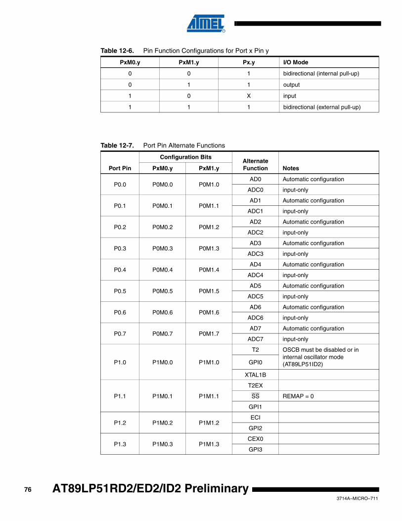
Table 12-6. Pin Function Configurations for Port x Pin y
PxM0.y PxM1.y Px.y I/O Mode
0 0 1 bidirectional (internal pull-up)
0 1 1 output
1 0 X input
1 1 1 bidirectional (external pull-up)
Table 12-7. Port Pin Alternate Functions
Port Pin
Configuration BitsAlternateFunction NotesPxM0.y PxM1.y
P0.0 P0M0.0 P0M1.0AD0 Automatic configuration
ADC0 input-only
P0.1 P0M0.1 P0M1.1AD1 Automatic configuration
ADC1 input-only
P0.2 P0M0.2 P0M1.2AD2 Automatic configuration
ADC2 input-only
P0.3 P0M0.3 P0M1.3AD3 Automatic configuration
ADC3 input-only
P0.4 P0M0.4 P0M1.4AD4 Automatic configuration
ADC4 input-only
P0.5 P0M0.5 P0M1.5AD5 Automatic configuration
ADC5 input-only
P0.6 P0M0.6 P0M1.6AD6 Automatic configuration
ADC6 input-only
P0.7 P0M0.7 P0M1.7AD7 Automatic configuration
ADC7 input-only
P1.0 P1M0.0 P1M1.0
T2 OSCB must be disabled or in internal oscillator mode (AT89LP51ID2)GPI0
XTAL1B
P1.1 P1M0.1 P1M1.1
T2EX
SS REMAP = 0
GPI1
P1.2 P1M0.2 P1M1.2ECI
GPI2
P1.3 P1M0.3 P1M1.3CEX0
GPI3
763714A–MICRO–711
AT89LP51RD2/ED2/ID2 Preliminary

AT89LP51RD2/ED2/ID2 Preliminary
P1.4 P1M0.4 P1M1.4
SS REMAP = 1
GPI4
CEX1
P1.5 P1M0.5 P1M1.5
MISO REMAP = 0
MOSI REMAP = 1
CEX2
GPI5
P1.6 P1M0.6 P1M1.6
SCK REMAP = 0
MISO REMAP = 1
CEX3
GPI6
P1.7 P1M0.7 P1M1.7
MOSI REMAP = 0
SCK REMAP = 1
CEX4
GPI7
P2.0 P2M0.0 P2M1.0 A8
P2.1 P2M0.1 P2M1.1 A9
P2.2 P2M0.2 P2M1.2A10
DA+ input-only
P2.3 P2M0.3 P2M1.3A11
DA- input-only
P2.4 P2M0.4 P2M1.4A12
AIN0 input-only
P2.5 P2M0.5 P2M1.5A13
AIN1 input-only
P2.6 P2M0.6 P2M1.6A14
AIN2 input-only
P2.7 P2M0.7 P2M1.7A15
AIN3 input-only
P3.0 P3M0.0 P3M1.0 RXD
P3.1 P3M0.1 P3M1.1 TXD
P3.2 P3M0.2 P3M1.2 INT0
P3.3 P3M0.3 P3M1.3 INT1
P3.4 P3M0.4 P3M1.4 T0
P3.5 P3M0.5 P3M1.5 T1
P3.6 P3M0.6 P3M1.6 WR
Table 12-7. Port Pin Alternate Functions
Port Pin
Configuration BitsAlternateFunction NotesPxM0.y PxM1.y
773714A–MICRO–711

P3.7 P3M0.7 P3M1.7 RD
P4.0 P4M0.0 P4M1.0 SCL open-drain
P4.1 P4M0.1 P4M1.1 SDA open-drain
P4.2 P4M0.2 P4M1.2 XTAL2BOSCB must be disabled or in internal oscillator or external clock modes to use P4.2(AT89LP51ID2)
P4.4 P4M0.4 P4M1.4 ALE Set AO in AUXR to use P4.4
P4.5 P4M0.5 P4M1.5 PSEN
P4.6 P4M0.6 P4M1.6 XTAL1AOSCA must be set to internal RC mode to use P4.6
P4.7 P4M0.7 P4M1.7 XTAL2AOSCA must be set to internal RC or external clock modes to use P4.7
Table 12-7. Port Pin Alternate Functions
Port Pin
Configuration BitsAlternateFunction NotesPxM0.y PxM1.y
783714A–MICRO–711
AT89LP51RD2/ED2/ID2 Preliminary

AT89LP51RD2/ED2/ID2 Preliminary
13. Enhanced Timer 0 and Timer 1 with PWMThe AT89LP51RD2/ED2/ID2 has two 16-bit Timer/Counters, Timer 0 and Timer 1, with the fol-lowing features:
• Two 16-bit timer/counters with 16-bit reload registers
• Two independent 8-bit precision PWM outputs with 8-bit prescalers
• UART or SPI baud rate generation using Timer 1
• Output pin toggle on timer overflow
• Split timer mode allows for three separate timers (2 8-bit, 1 16-bit)
• Gated modes allow timers to run/halt based on an external input
Timer 0 and Timer 1 have similar modes of operation. As timers, the timer registers normallyincrease every clock cycle. Thus, the registers count clock cycles. The timer rate can be pres-caled by a value between 1 and 16 using the Timer Prescaler (see Section 6.9 on page 50).Both Timers share the same prescaler. In Compatibility mode the prescaler is always enabledand TPS defaults to 5, so the timers count every six clock cycles (1/12 of the oscillator frequencyin X1 mode or 1/6 of the oscillator frequency in X2 mode). In X2 mode the timers can be set tothe X1 rate by setting the T0X2 or T1X2 bits in CKCON1. In Fast mode the prescaler is notenabled by default so the count rate is equal to the system frequency (1/2 of the oscillator fre-quency in X1 mode or equal to the oscillator frequency in X2 mode). In this case setting theT0X2 or T1X2 bits in CKCON1 enables the prescaler for each timer.
As counters, the timer registers are incremented in response to a 1-to-0 transition at the corre-sponding input pins, T0 or T1. In Fast mode the external input is sampled every clock cycle.When the samples show a high in one cycle and a low in the next cycle, the count is incre-mented. The new count value appears in the register during the cycle following the one in whichthe transition was detected. Since 2 clock cycles are required to recognize a 1-to-0 transition,the maximum count rate is 1/2 of the system frequency. There are no restrictions on the dutycycle of the input signal, but it should be held for at least one full clock cycle to ensure that agiven level is sampled at least once before it changes.
In Compatibility mode the counter input sampling is controlled by the prescaler. Since TPSdefaults to 6 in this mode, the pins are sampled every six system clocks. Therefore the input sig-nal should be held for at least six clock cycles to ensure that a given level is sampled at leastonce before it changes.
Furthermore, the Timer or Counter functions for Timer 0 and Timer 1 have four operating modes:13-bit timer, 16-bit timer, 8-bit auto-reload timer, and split timer. The control bits C/T in the Spe-cial Function Register TMOD select the Timer or Counter function. The bit pairs (M1, M0) inTMOD select the operating modes.
fTIMERfSYS
2TnX2 TPS 1+( )×------------------------------------------------= Compatibility Mode
fTIMERfSYS
TPS 1+---------------------= Fast Mode and TnX2 = 1
fTIMER fSYS= Fast Mode and TnX2 = 0
793714A–MICRO–7/11

13.1 RegistersTable 13-1 lists the registers used by Timer 0/1. TCON, TCONB and TMOD are detailed below.
Note: The RHn/RLn registers are not required by the Timer during Modes 0, 2 or 3 and may be used as temporary storage registers in these modes, except when using the PWM generator.
.
Table 13-1. Timer 0/1 Register Summary
Name Address Purpose Bit-Addressable
TCON 88H Control Y
TMOD 89H Mode N
TL0 8AH Timer 0 low-byte N
TL1 8BH Timer 1 low-byte N
TH0 8CH Timer 0 high-byte N
TH1 8DH Timer 1 high-byte N
TCONB 91H Mode N
RL0 F2H Timer 0 reload low-byte N
RL1 F3H Timer 1 reload low-byte N
RH0 F4H Timer 0 reload high-byte N
RH1 F5H Timer 1 reload high-byte N
Table 13-2. TCON – Timer/Counter Control Register
TCON = 88H Reset Value = 0000 0000B
Bit Addressable
TF1 TR1 TF0 TR0 IE1 IT1 IE0 IT0
Bit 7 6 5 4 3 2 1 0
Symbol Function
TF1Timer 1 Overflow FlagSet by hardware on Timer/Counter overflow. Cleared by hardware when the processor vectors to interrupt routine.
TR1Timer 1 Run ControlSet/cleared by software to turn Timer/Counter on/off.
TF0Timer 0 Overflow FlagSet by hardware on Timer/Counter overflow. Cleared by hardware when the processor vectors to interrupt routine.
TR0Timer 0 Run ControlSet/cleared by software to turn Timer/Counter on/off.
IE1Interrupt 1 Edge FlagSet by hardware when external interrupt edge detected. Cleared when interrupt processed.
IT1Interrupt 1 TypeSet/cleared by software to specify falling edge/low level triggered external interrupts.
IE0Interrupt 0 Edge FlagSet by hardware when external interrupt edge detected. Cleared when interrupt processed.
IT0Interrupt 0 TypeSet/cleared by software to specify falling edge/low level triggered external interrupts.
803714A–MICRO–7/11
AT89LP51RD2/ED2/ID2 Preliminary

AT89LP51RD2/ED2/ID2 Preliminary
Table 13-3. TMOD – Timer/Counter Mode Control Register
TMOD Address = 089H Reset Value = 0000 0000B
Not Bit Addressable
GATE1 C/T1 T1M1 T1M0 GATE0 C/T0 T0M0 T0M1
Bit 7 6 5 4 3 2 1 0
Symbol Function
GATE1Timer 1 Gating ControlWhen set, Timer/Counter 1 is enabled only while INT1 pin is high and TR1 control pin is set. When cleared, Timer 1 is enabled whenever TR1 control bit is set.
C/T1Timer or Counter Selector 1Cleared for Timer operation (input from internal system clock). Set for Counter operation (input from T1 input pin). C/T1 must be zero when using Timer 1 in PWM output mode.
T1M1T1M0
Timer 1 Operating Mode
Mode T1M1 T1M0 Operation
0 0 0Variable Timer Mode. 8-bit Timer/Counter TH1 with TL1 as 1–8 bit prescaler. Default is 5 bits for a 13-bit timer/counter compatible with AT89C51RD2/ED2/ID2.
1 0 116-bit Auto-Reload Mode. TH1 and TL1 are cascaded to form a 16-bit Timer/Counter which is reloaded from RH1 and RL1 when it overflows.
2 1 08-bit Auto-Reload Mode. TH1 holds a value which is reloaded into 8-bit Timer/Counter TL1 each time it overflows.
3 1 1 Timer/Counter 1 is stopped
GATE0Timer 0 Gating ControlWhen set, Timer/Counter 0 is enabled only while INT0 pin is high and TR0 control pin is set. When cleared, Timer 0 is enabled whenever TR0 control bit is set.
C/T0Timer or Counter Selector 0Cleared for Timer operation (input from internal system clock). Set for Counter operation (input from T0 input pin). C/T0 must be zero when using Timer 0 in PWM output mode.
T0M1T0M0
Timer 0 Operating Mode
Mode T0M1 T0M0 Operation
0 0 0Variable Timer Mode. 8-bit Timer/Counter TH0 with TL0 as 1–8 bit prescaler. Default is 5 bits for a 13-bit timer/counter compatible with AT89C51RD2/ED2/ID2.
1 0 116-bit Auto-Reload Mode. TH0 and TL0 are cascaded to form a 16-bit Timer/Counter which is reloaded from RH0 and RL0 when it overflows.
2 1 08-bit Auto-Reload Mode. TH0 holds a value which is reloaded into 8-bit Timer/Counter TL0 each time it overflows.
3 1 1Split Timer Mode. TL0 is an 8-bit Timer/Counter controlled by the standard Timer 0 control bits. TH0 is only an 8-bit timer controlled by Timer 1 control bits.
813714A–MICRO–7/11
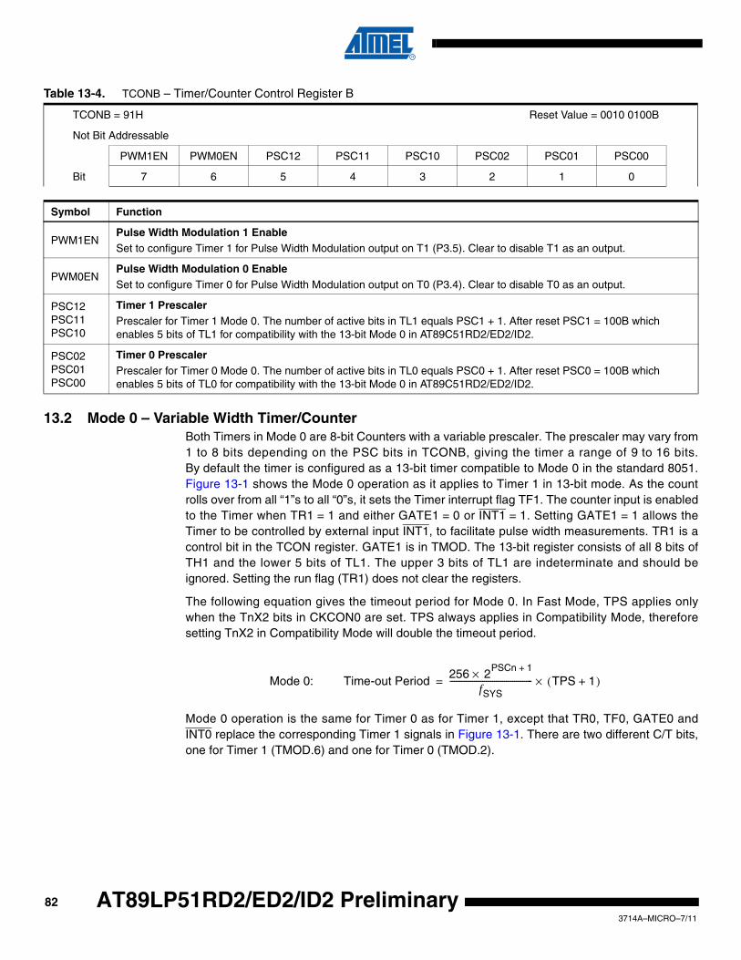
13.2 Mode 0 – Variable Width Timer/CounterBoth Timers in Mode 0 are 8-bit Counters with a variable prescaler. The prescaler may vary from1 to 8 bits depending on the PSC bits in TCONB, giving the timer a range of 9 to 16 bits.By default the timer is configured as a 13-bit timer compatible to Mode 0 in the standard 8051.Figure 13-1 shows the Mode 0 operation as it applies to Timer 1 in 13-bit mode. As the countrolls over from all “1”s to all “0”s, it sets the Timer interrupt flag TF1. The counter input is enabledto the Timer when TR1 = 1 and either GATE1 = 0 or INT1 = 1. Setting GATE1 = 1 allows theTimer to be controlled by external input INT1, to facilitate pulse width measurements. TR1 is acontrol bit in the TCON register. GATE1 is in TMOD. The 13-bit register consists of all 8 bits ofTH1 and the lower 5 bits of TL1. The upper 3 bits of TL1 are indeterminate and should beignored. Setting the run flag (TR1) does not clear the registers.
The following equation gives the timeout period for Mode 0. In Fast Mode, TPS applies onlywhen the TnX2 bits in CKCON0 are set. TPS always applies in Compatibility Mode, thereforesetting TnX2 in Compatibility Mode will double the timeout period.
Mode 0 operation is the same for Timer 0 as for Timer 1, except that TR0, TF0, GATE0 andINT0 replace the corresponding Timer 1 signals in Figure 13-1. There are two different C/T bits,one for Timer 1 (TMOD.6) and one for Timer 0 (TMOD.2).
Table 13-4. TCONB – Timer/Counter Control Register B
TCONB = 91H Reset Value = 0010 0100B
Not Bit Addressable
PWM1EN PWM0EN PSC12 PSC11 PSC10 PSC02 PSC01 PSC00
Bit 7 6 5 4 3 2 1 0
Symbol Function
PWM1ENPulse Width Modulation 1 EnableSet to configure Timer 1 for Pulse Width Modulation output on T1 (P3.5). Clear to disable T1 as an output.
PWM0ENPulse Width Modulation 0 EnableSet to configure Timer 0 for Pulse Width Modulation output on T0 (P3.4). Clear to disable T0 as an output.
PSC12PSC11PSC10
Timer 1 PrescalerPrescaler for Timer 1 Mode 0. The number of active bits in TL1 equals PSC1 + 1. After reset PSC1 = 100B which enables 5 bits of TL1 for compatibility with the 13-bit Mode 0 in AT89C51RD2/ED2/ID2.
PSC02PSC01PSC00
Timer 0 PrescalerPrescaler for Timer 0 Mode 0. The number of active bits in TL0 equals PSC0 + 1. After reset PSC0 = 100B which enables 5 bits of TL0 for compatibility with the 13-bit Mode 0 in AT89C51RD2/ED2/ID2.
Mode 0: Time-out Period256 2
PSCn 1+×fSYS
----------------------------------------- TPS 1+( )×=
823714A–MICRO–7/11
AT89LP51RD2/ED2/ID2 Preliminary

AT89LP51RD2/ED2/ID2 Preliminary
Figure 13-1. Timer/Counter 1 Mode 0: Variable Width Counter
13.3 Mode 1 – 16-bit Auto-Reload Timer/CounterIn Mode 1 the Timers are configured for 16-bit auto-reload. The Timer register is run with all16 bits. The 16-bit reload value is stored in the high and low reload registers (RH1/RL1). Theclock is applied to the combined high and low timer registers (TH1/TL1). As clock pulses arereceived, the timer counts up: 0000H, 0001H, 0002H, etc. An overflow occurs on the FFFFH-to-0000H transition, upon which the timer register is reloaded with the value from RH1/RL1 and theoverflow flag bit in TCON is set. See Figure 13-2. The reload registers default to 0000H, whichgives the full 16-bit timer period compatible with the standard 8051. Mode 1 operation is thesame for Timer/Counter 0.
The following equation gives the timeout period for Mode 1. In Fast Mode, TPS applies onlywhen the TnX2 bits in CKCON0 are set. TPS always applies in Compatibility Mode, thereforesetting TnX2 in Compatibility Mode will double the timeout period.
Figure 13-2. Timer/Counter 1 Mode 1: 16-bit Auto-Reload
CLKSYS
T1 Pin
TR1
GATE1
INT1 Pin
TL1 (8 Bits)
Control
Inter r up t
C/T = 0
C/T = 1
PSC1
TH1 (8 Bits) TF1
÷TPS
Mode 1: Time-out Period65536 RHn RLn{ , }–( )
fSYS--------------------------------------------------------- TPS 1+( )×=
CLKSYS
T1 Pin
TR1
GATE1
INT1 Pin
TL1 (8 Bits)
Control
Inter r up t
C/T = 0
C/T =1
TH1 (8 Bits) TF1
RL1 (8 Bits)
RH1 (8 Bits)
Reload ÷TPS
833714A–MICRO–7/11

13.4 Mode 2 – 8-bit Auto-Reload Timer/CounterMode 2 configures the Timer register as an 8-bit Counter (TL1) with automatic reload, as shownin Figure 13-3. Overflow from TL1 not only sets TF1, but also reloads TL1 with the contents ofTH1, which is preset by software. The reload leaves TH1 unchanged. Mode 2 operation is thesame for Timer/Counter 0.
The following equation gives the timeout period for Mode 2. In Fast Mode, TPS applies onlywhen the TnX2 bits in CKCON0 are set. TPS always applies in Compatibility Mode, thereforesetting TnX2 in Compatibility Mode will double the timeout period.
Figure 13-3. Timer/Counter 1 Mode 2: 8-bit Auto-Reload
Note: RH1/RL1 are not required by Timer 1 during Mode 2 and may be used as temporary storage registers.
13.5 Mode 3 – 8-bit Split TimerTimer 1 in Mode 3 simply holds its count. The effect is the same as setting TR1 = 0. Timer 0 inMode 3 establishes TL0 and TH0 as two separate counters. The logic for Mode 3 on Timer 0 isshown in Figure 13-4. TL0 uses the Timer 0 control bits: C/T, GATE0, TR0, INT0, and TF0. TH0is locked into a timer function (counting clock cycles) and takes over the use of TR1 and TF1from Timer 1. Thus, TH0 now controls the Timer 1 interrupt. While Timer 0 is in Mode 3, Timer 1will still obey its settings in TMOD but cannot generate an interrupt.
Mode 3 is for applications requiring an extra 8-bit timer or counter. With Timer 0 in Mode 3, theAT89LP51RD2/ED2/ID2 can appear to have four Timer/Counters. When Timer 0 is in Mode 3,Timer 1 can be turned on and off by switching it out of and into its own Mode 3. In this case,Timer 1 can still be used by the serial port as a baud rate generator or in any application notrequiring an interrupt.
The following equation gives the timeout period for Mode 3. In Fast Mode, TPS applies onlywhen the TnX2 bits in CKCON0 are set. TPS always applies in Compatibility Mode, thereforesetting TnX2 in Compatibility Mode will double the timeout period.
Mode 2: Time-out Period256 THn–( )
fSYS-------------------------------- TPS 1+( )×=
CLKSYS
T1 Pin
TR1
GATE1
TF1 TL1 (8 Bits)
TH1 (8 Bits)
Control Reload
Inter r up t
INT0 Pin
C/T = 0
C/T = 1
÷TPS
Mode 3: Time-out Period256fSYS----------- TPS 1+( )×=
843714A–MICRO–7/11
AT89LP51RD2/ED2/ID2 Preliminary

AT89LP51RD2/ED2/ID2 Preliminary
Figure 13-4. Timer/Counter 0 Mode 3: Two 8-bit Counters
13.6 Pulse Width ModulationOn the AT89LP51RD2/ED2/ID2, Timer 0 and Timer 1 may be independently configured as 8-bitasymmetrical (edge-aligned) pulse width modulators (PWM) by setting the PWM0EN orPWM1EN bits in TCONB, respectively. In PWM Mode the generated waveform is output on thetimer's input pin, T0 or T1. Therefore, C/Tx must be set to “0” when in PWM mode and the T0(P3.4) and T1 (P3.5) must be configured in an output mode. The Timer Overflow Flags andInterrupts will continue to function while in PWM Mode and Timer 1 may still generate the baudrate for the UART. The timer GATE function also works in PWM mode, allowing the output to behalted by an external input. Each PWM channel has four modes selected by the mode bits inTMOD.
An example waveform for Timer 0 in PWM Mode 0 is shown in Figure 13-5. TH0 acts as an 8-bitcounter while RH0 stores the 8-bit compare value. When TH0 is 00H the PWM output isset high. When the TH0 count reaches the value stored in RH0 the PWM output is set low.Therefore, the pulse width is proportional to the value in RH0. To prevent glitches, writes toRH0 only take effect on the FFH to 00H overflow of TH0. Setting RH0 to 00H will keep the PWMoutput low.
Figure 13-5. 8-bit Asymmetrical Pulse Width Modulation
Control
Inter r up t
Control
Inter r up t (8 Bits)
(8 Bits)
C/T = 0
C/T =1 T0 Pin
GATE0
INT0 Pin
÷TPS
÷TPS
CLKSYS
CLKSYS
FFH
00H
RH0
(P3.4)T0
TF0 SetTH0
time
853714A–MICRO–7/11

13.6.1 Mode 0 – 8-bit PWM with 8-bit Logarithmic PrescalerIn Mode 0, TLn acts as a logarithmic prescaler driving 8-bit counter THn (see Figure 13-6). ThePSCn bits in TCONB control the prescaler value. On THn overflow, the duty cycle value in RHnis transferred to OCRn and the output pin is set high. When the count in THn matches OCRn,the output pin is cleared low. The following formulas give the output frequency and duty cycle forTimer n in PWM Mode 0. Timer 1 in PWM Mode 0 is identical to Timer 0.
Note: In Fast Mode, TPS applies only when the TnX2 bits in CKCON0 are set. TPS always applies in Compatibility Mode, therefore setting TnX2 in Compatibility Mode will halve the output frequency.
Figure 13-6. Timer/Counter 1 PWM Mode 0
13.6.2 Mode 1 – 8-bit PWM with 8-bit Linear PrescalerIn Mode 1, TLn provides linear prescaling with an 8-bit auto-reload from RLn (see Figure 13-7 onpage 87). On TLn overflow, TLn is loaded with the value of RLn. THn acts as an 8-bit counter.On THn overflow, the duty cycle value in RHn is transferred to OCRn and the output pin is sethigh. When the count in THn matches OCRn, the output pin is cleared low. The following formu-las give the output frequency and duty cycle for Timer n in PWM Mode 1. Timer 1 in PWM Mode1 is identical to Timer 0.
Note: In Fast Mode, TPS applies only when the TnX2 bits in CKCON0 are set. TPS always applies in Compatibility Mode, therefore setting TnX2 in Compatibility Mode will halve the output frequency.
Mode 0:fout
fSYS
256 2PSCn 1+×
----------------------------------------- 1TPS 1+---------------------×=
Duty Cycle % 100RHn256------------×=
CLKSYS
TR1
GATE1
INT1 Pin
TL1 (8 Bits)
Control
PSC1 TH1 (8 Bits)
OCR1
RH1 (8 Bits)
= T1
÷TPS
Mode 1:fout
fSYS
256 256 RLn–( )×------------------------------------------------- 1
TPS 1+---------------------×=
Duty Cycle % 100RHn256------------×=
863714A–MICRO–7/11
AT89LP51RD2/ED2/ID2 Preliminary
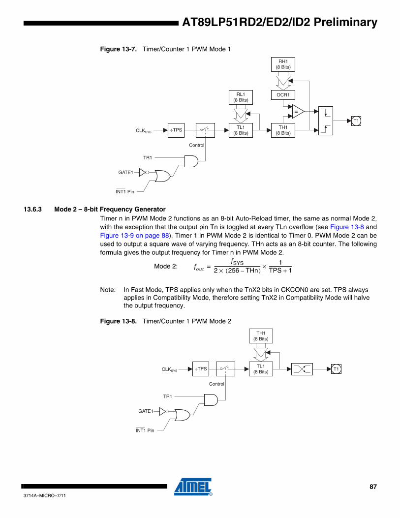
AT89LP51RD2/ED2/ID2 Preliminary
Figure 13-7. Timer/Counter 1 PWM Mode 1
13.6.3 Mode 2 – 8-bit Frequency GeneratorTimer n in PWM Mode 2 functions as an 8-bit Auto-Reload timer, the same as normal Mode 2,with the exception that the output pin Tn is toggled at every TLn overflow (see Figure 13-8 andFigure 13-9 on page 88). Timer 1 in PWM Mode 2 is identical to Timer 0. PWM Mode 2 can beused to output a square wave of varying frequency. THn acts as an 8-bit counter. The followingformula gives the output frequency for Timer n in PWM Mode 2.
Note: In Fast Mode, TPS applies only when the TnX2 bits in CKCON0 are set. TPS always applies in Compatibility Mode, therefore setting TnX2 in Compatibility Mode will halve the output frequency.
Figure 13-8. Timer/Counter 1 PWM Mode 2
CLKSYS
TR1
GATE1
INT1 Pin
TL1 (8 Bits)
Control
TH1 (8 Bits)
OCR1
RH1 (8 Bits)
= T1
RL1 (8 Bits)
÷TPS
Mode 2: foutfSYS
2 256 THn–( )×------------------------------------------ 1
TPS 1+---------------------×=
CLKSYS
TR1
GATE1
INT1 Pin
TL1 (8 Bits)
Control
T1
TH1 (8 Bits)
÷TPS
873714A–MICRO–7/11

Figure 13-9. PWM Mode 2 Waveform
13.6.4 Mode 3 – Split 8-bit PWMTimer 1 in PWM Mode 3 simply holds its count. The effect is the same as setting TR1 = 0.Timer 0 in PWM Mode 3 establishes TL0 and TH0 as two separate PWM counters in a mannersimilar to normal Mode 3. PWM Mode 3 on Timer 0 is shown in Figure 13-10. Only the TimerPrescaler is available to change the output frequency during PWM Mode 3. TL0 can use theTimer 0 control bits: GATE, TR0, INT0, PWM0EN and TF0. TH0 is locked into a timer functionand uses TR1, PWM1EN and TF1. RL0 provides the duty cycle for TL0 and RH0 provides theduty cycle for TH0.
PWM Mode 3 is for applications requiring a single PWM channel and two timers, or two PWMchanne ls and an ex t ra t imer o r coun te r . Wi th T imer 0 in PWM Mode 3 , theAT89LP51RD2/ED2/ID2 can appear to have four Timer/Counters. When Timer 0 is in PWMMode 3, Timer 1 can be turned on and off by switching it out of and into its own Mode 3. In thiscase, Timer 1 can still be used by the serial port as a baud rate generator or in any applicationnot requiring an interrupt. The following formulas give the output frequency and duty cycle forTimer 0 in PWM Mode 3.
Note: In Fast Mode, TPS applies only when the TnX2 bits in CKCON0 are set. TPS always applies in Compatibility Mode, therefore setting TnX2 in Compatibility Mode will halve the output frequency.
Tx
THx
FFh
Mode 3: foutfSYS
256----------- 1
TPS 1+---------------------×=
Mode 3, T0: Duty Cycle % 100RL0256-----------×=
Mode 3, T1: Duty Cycle % 100RH0256------------×=
883714A–MICRO–7/11
AT89LP51RD2/ED2/ID2 Preliminary
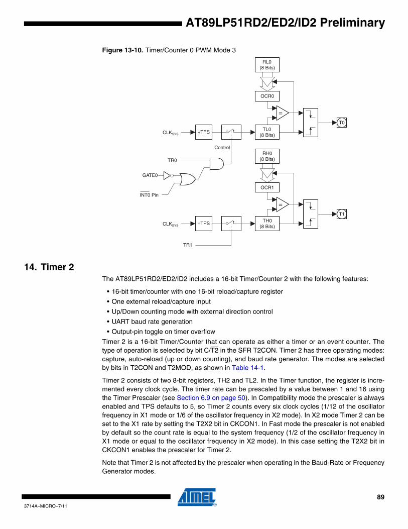
AT89LP51RD2/ED2/ID2 Preliminary
Figure 13-10. Timer/Counter 0 PWM Mode 3
14. Timer 2The AT89LP51RD2/ED2/ID2 includes a 16-bit Timer/Counter 2 with the following features:
• 16-bit timer/counter with one 16-bit reload/capture register
• One external reload/capture input
• Up/Down counting mode with external direction control
• UART baud rate generation
• Output-pin toggle on timer overflow
Timer 2 is a 16-bit Timer/Counter that can operate as either a timer or an event counter. Thetype of operation is selected by bit C/T2 in the SFR T2CON. Timer 2 has three operating modes:capture, auto-reload (up or down counting), and baud rate generator. The modes are selectedby bits in T2CON and T2MOD, as shown in Table 14-1.
Timer 2 consists of two 8-bit registers, TH2 and TL2. In the Timer function, the register is incre-mented every clock cycle. The timer rate can be prescaled by a value between 1 and 16 usingthe Timer Prescaler (see Section 6.9 on page 50). In Compatibility mode the prescaler is alwaysenabled and TPS defaults to 5, so Timer 2 counts every six clock cycles (1/12 of the oscillatorfrequency in X1 mode or 1/6 of the oscillator frequency in X2 mode). In X2 mode Timer 2 can beset to the X1 rate by setting the T2X2 bit in CKCON1. In Fast mode the prescaler is not enabledby default so the count rate is equal to the system frequency (1/2 of the oscillator frequency inX1 mode or equal to the oscillator frequency in X2 mode). In this case setting the T2X2 bit inCKCON1 enables the prescaler for Timer 2.
Note that Timer 2 is not affected by the prescaler when operating in the Baud-Rate or FrequencyGenerator modes.
CLKSYS
TR0
GATE0
INT0 Pin
Control
TL0 (8 Bits)
OCR0
RL0 (8 Bits)
= T0
CLKSYSTH0 (8 Bits)
OCR1
RH0 (8 Bits)
= T1
TR1
÷TPS
÷TPS
893714A–MICRO–7/11

Note: In Fast Mode, TPS applies only when the T2X2 bit in CKCON0 is set. TPS always applies in Compatibility Mode, therefore setting T2X2 in Compatibility Mode will halve the timer frequency.
In the Counter function, the register is incremented in response to a 1-to-0 transition at its corre-sponding external input pin, T2. In Fast mode the external input is sampled every clock cycle.When the samples show a high in one cycle and a low in the next cycle, the count is incre-mented. The new count value appears in the register during the cycle following the one in whichthe transition was detected. Since 2 clock cycles are required to recognize a 1-to-0 transition,the maximum count rate is 1/2 of the system frequency. There are no restrictions on the dutycycle of the input signal, but it should be held for at least one full clock cycle to ensure that agiven level is sampled at least once before it changes.
In Compatibility mode the counter input sampling is controlled by the prescaler. Since TPSdefaults to 6 in this mode, the pins are sampled every six system clocks. Therefore the input sig-nal should be held for at least six clock cycles to ensure that a given level is sampled at leastonce before it changes.
The following definitions for Timer 2 are used in the subsequent paragraphs:
Table 14-1. Timer 2 Operating Modes
RCLK + TCLK CP/RL2 DCEN T2OE TR2 MODE
0 0 0 0 1 16-bit Auto-reload
0 0 1 0 1 16-bit Auto-reload Up-Down
0 1 X 0 1 16-bit Capture
1 X X X 1 Baud Rate Generator
X X X 1 1 Frequency Generator
X X X X 0 (Off)
Table 14-2. Timer 2 Definitions
Symbol Definition
MIN 0000H
MAX FFFFH
BOTTOM 16-bit value of {RCAP2H,RCAP2L}
fTIMERfSYS
2T2X2 TPS 1+( )×------------------------------------------------= Compatibility Mode
fTIMERfSYS
TPS 1+---------------------= Fast Mode and T2X2 = 1
fTIMER fSYS= Fast Mode and T2X2 = 0
903714A–MICRO–7/11
AT89LP51RD2/ED2/ID2 Preliminary

AT89LP51RD2/ED2/ID2 Preliminary
14.1 Timer 2 RegistersControl and status bits for Timer 2 are contained in registers T2CON (see Table 14-3) andT2MOD (see Table 14-4). The register pair {TH2, TL2} at addresses 0CDH and 0CCH are the16-bit timer register for Timer 2. The register pair {RCAP2H, RCAP2L} at addresses 0CBH and0CAH are the 16-bit Capture/Reload register for Timer 2 in capture and auto-reload modes.
Note: The Timer 2 operating mode depends on bits in both T2CON and T2MOD as shown in Table 14-1. The RCLK, TCLK and T2OE bits have priority over CP/RL2.
Table 14-3. T2CON – Timer/Counter 2 Control Register
T2CON Address = 0C8H Reset Value = 0000 0000B
Bit Addressable
TF2 EXF2 RCLK TCLK EXEN2 TR2 C/T2 CP/RL2
Bit 7 6 5 4 3 2 1 0
Symbol Function
TF2Timer 2 Overflow FlagSet by hardware when Timer 2 overflows and must be cleared by software. TF2 will not be set when either RCLK = 1 or TCLK = 1. TF2 will generate an interrupt when ET2 is set in IEN0.
EXF2
Timer 2 External FlagSet when either a capture or reload is caused by a negative transition on T2EX and EXEN2 = 1. When Timer 2 interrupt is enabled, EXF2 = 1 will cause the CPU to vector to the Timer 2 interrupt routine. EXF2 must be cleared by software. EXF2 does not cause an interrupt in up/down counter mode (DCEN = 1) or dual-slope mode.
RCLKReceive Clock EnableSet to use Timer 2 overflow pulses for receive clock in serial port Modes 1 and 3. Clear to use Timer 1 overflows for the receive clock.
TCLKTransmit Clock EnableSet to use Timer 2 overflow pulses for transmit clock in serial port Modes 1 and 3. Clear to use Timer 1 overflows for the transmit clock.
EXEN2Timer 2 External EnableWhen set, allows a capture or reload to occur as a result of a negative transition on T2EX if Timer 2 is not being used to clock the serial port. EXEN2 = 0 causes Timer 2 to ignore events at T2EX.
TR2Timer 2 Run ControlStart/Stop control for Timer 2. TR2 = 1 starts the timer. TR2 = 0 stops the timer.
C/T2Timer/Counter Select 2Clear C/T2 = 0 for timer function. Set C/T2 = 1 for external event counter on T2 (P1.0) (falling edge triggered). C/T2 must be 0 to use clock out mode.
CP/RL2
Capture/Reload SelectCP/RL2 = 1 causes captures to occur on negative transitions at T2EX if EXEN2 = 1. CP/RL2 = 0 causes automatic reloads to occur when Timer 2 overflows or negative transitions occur at T2EX when EXEN2 = 1. When either RCLK or TCLK = 1, this bit is ignored and the timer is forced to auto-reload on Timer 2 overflow.
913714A–MICRO–7/11

14.2 Capture ModeIn the Capture mode, Timer 2 is a fixed 16-bit timer or counter that counts up from MIN to MAX.An overflow from MAX to MIN sets bit TF2 in T2CON. If EXEN2 = 1, a 1-to-0 transition at exter-nal input T2EX also causes the current value in TH2 and TL2 to be captured into RCAP2H andRCAP2L, respectively. In addition, the transition at T2EX causes bit EXF2 in T2CON to be set.The EXF2 and TF2 bits can generate an interrupt. Capture mode is illustrated in Figure 14-1.The Timer 2 overflow rate in Capture mode is given by the following equation:
Note: In Fast Mode, TPS applies only when the T2X2 bit in CKCON0 is set. TPS always applies in Compatibility Mode, therefore setting T2X2 in Compatibility Mode will double the timeout period.
Figure 14-1. Timer 2 Diagram: Capture Mode
Table 14-4. T2MOD – Timer 2 Mode Control Register
T2MOD Address = 0C9H Reset Value = 0000 0000B
Not Bit Addressable
– – – – – – T2OE DCEN
Bit 7 6 5 4 3 2 1 0
Symbol Function
T2OE Timer 2 Output EnableWhen T2OE = 1 and C/T2 = 0, the T2 pin will toggle after every Timer 2 overflow.
DCEN Timer 2 Down Count EnableWhen Timer 2 operates in Auto-Reload mode and EXEN2 = 1, setting DCEN = 1 will cause Timer 2 to count up or down depending on the state of T2EX.
Capture Mode: Time-out Period65536fSYS
---------------- TPS 1+( )×=
÷TPS
EXF2 T2EX PI N
T2 PI N
TR2
EXEN2
C/T2 = 0
C/T2 = 1
CAPTURE
O VERFLO W
TRANSITION DETECT OR TIMER 2
INTERR UPT
RCAP2H RCAP2L
TL2 TH2 TF2
CLKSYS
923714A–MICRO–7/11
AT89LP51RD2/ED2/ID2 Preliminary

AT89LP51RD2/ED2/ID2 Preliminary
14.3 Auto-Reload ModeTimer 2 can be programmed to count up or down when configured in its 16-bit auto-reloadmode. This feature is invoked by the DCEN (Down Counter Enable) bit located in the SFRT2MOD (see Table 14-4). Upon reset, the DCEN bit is set to 0 so that timer 2 will default tocount up. When DCEN is set, Timer 2 can count up or down, depending on the value of theT2EX pin. A summary of the Auto-Reload behaviors is listed in Table 14-5.
14.3.1 Up CounterFigure 14-2 shows Timer 2 automatically counting up when DCEN = 0. In this mode Timer 2counts up to MAX and then sets the TF2 bit upon overflow. The overflow also causes the timerregisters to be reloaded with BOTTOM, the 16-bit value in RCAP2H and RCAP2L. If EXEN2 = 1,a 16-bit reload can be triggered either by an overflow or by a 1-to-0 transition at external inputT2EX. This transition also sets the EXF2 bit. Both the TF2 and EXF2 bits can generate an inter-rupt. The Timer 2 overflow rate for this mode is given in the following equation:
Note: In Fast Mode, TPS applies only when the T2X2 bit in CKCON0 is set. TPS always applies in Compatibility Mode, therefore setting T2X2 in Compatibility Mode will double the timeout period.
Figure 14-2. Timer 2 Diagram: Auto-Reload Mode (DCEN = 0)
Table 14-5. Summary of Auto-Reload Modes
DCEN T2EX Direction Behavior
0 X Up reload to BOTTOM
1 0 Down underflow to MAX
1 1 Up overflow to BOTTOM
BOTTOM MAX→
MAX BOTTOM→
BOTTOM MAX→
Auto-Reload Mode:
DCEN = 0Time-out Period
65536 RCAP2H RCAP2L{ , }–fSYS
------------------------------------------------------------------------------- TPS 1+( )×=
CLKSYS
TL2 TH2
÷TPS
933714A–MICRO–7/11

Figure 14-3. Timer 2 Waveform: Auto-Reload Mode (DCEN = 0)
14.3.2 Up or Down CounterSetting DCEN = 1 enables Timer 2 to count up or down, as shown in Figure 14-5. In this mode,the T2EX pin controls the direction of the count (if EXEN2 = 1). A logic 1 at T2EX makes Timer 2count up. When T2CM1-0 = 00B, the timer will overflow at MAX and set the TF2 bit. This overflowalso causes BOTTOM, the 16-bit value in RCAP2H and RCAP2L, to be reloaded into the timerregisters, TH2 and TL2, respectively. A logic 0 at T2EX makes Timer 2 count down. The timerunderflows when TH2 and TL2 equal BOTTOM, the 16-bit value stored in RCAP2H andRCAP2L. The underflow sets the TF2 bit and causes MAX to be reloaded into the timer regis-ters. The EXF2 bit toggles whenever Timer 2 overflows or underflows and can be used as a 17thbit of resolution. In this operating mode, EXF2 does not flag an interrupt.
The behavior of Timer 2 when DCEN is enabled is shown in Figure 14-4. The timer over-flow/underflow rate for up-down counting mode is the same as for up counting mode, providedthat the count direction does not change. Changes to the count direction may result in longer orshorter periods between time-outs.
Figure 14-4. Timer 2 Waveform: Auto-Reload Mode (DCEN = 1)
MAX
MIN
BOTTOM
TF2 Set
MAX
MIN
BOTTOM
T2EX
TF2 Set
EXF2
943714A–MICRO–7/11
AT89LP51RD2/ED2/ID2 Preliminary

AT89LP51RD2/ED2/ID2 Preliminary
Figure 14-5. Timer 2 Diagram: Auto-Reload Mode (DCEN = 1)
14.4 Baud Rate GeneratorTimer 2 is selected as the baud rate generator by setting TCLK and/or RCLK in T2CON (Table14-3). Note that the baud rates for transmit and receive can be different if Timer 2 is used for thereceiver or transmitter and Timer 1 is used for the other function. Setting RCLK and/or TCLKputs Timer 2 into its baud rate generator mode, as shown in Figure 14-6.
The baud rate generator mode is similar to the auto-reload mode, in that a rollover in TH2causes the Timer 2 registers to be reloaded with the 16-bit value in registers RCAP2H andRCAP2L, which are preset by software.
The baud rates in UART Modes 1 and 3 are determined by Timer 2’s overflow rate according tothe following equation.
The Timer can be configured for either timer or counter operation. In most applications, it is con-figured for timer operation (CP/T2 = 0). The baud rate formulas are given below.
where (RCAP2H, RCAP2L) is the content of RCAP2H and RCAP2L taken as a 16-bit unsignedinteger.
Timer 2 as a baud rate generator is shown in Figure 14-6. This figure is valid only if RCLK orTCLK = 1 in T2CON. Note that a rollover in TH2 does not set TF2 and will not generate an inter-rupt. Note too, that if EXEN2 is set, a 1-to-0 transition in T2EX will set EXF2 but will not cause areload from (RCAP2H, RCAP2L) to (TH2, TL2). Thus when Timer 2 is in use as a baud rate gen-erator, T2EX can be used as an extra external interrupt. Also note that the Baud Rate andFrequency Generator modes may be used simultaneously.
÷TPS CLKSYS
Modes 1 and 3 Baud Rates Timer 2 Overflow Rate16
------------------------------------------------------------=
Modes 1, 3
Baud Rate
fSYS
16 65536 RCAP2H,RCAP2L( )–[ ]×-----------------------------------------------------------------------------------------------=
953714A–MICRO–7/11

Figure 14-6. Timer 2 in Baud Rate Generator Mode
14.5 Frequency Generator (Programmable Clock Out)Timer 2 can generate a 50% duty cycle clock on T2 (P1.0). This pin, besides being a regular I/Opin, has two alternate functions. It can be programmed to input the external clock forTimer/Counter 2 or to toggle its output at every timer overflow. To configure the Timer/Counter 2as a clock generator, bit C/T2 (T2CON.1) must be cleared and bit T2OE (T2MOD.1) must beset. Bit TR2 (T2CON.2) starts and stops the timer. The clock-out frequency depends on the sys-tem frequency and the reload value of Timer 2 capture registers (RCAP2H, RCAP2L), as shownin the following equation.
In the frequency generator mode, Timer 2 roll-overs will not generate an interrupt. This behavioris similar to when Timer 2 is used as a baud-rate generator. It is possible to use Timer 2 as abaud-rate generator and a clock generator simultaneously. Note, however, that the baud-rateand clock-out frequencies cannot be determined independently from one another since theyboth use RCAP2H and RCAP2L.
Figure 14-7. Timer 2 in Clock-out Mode
SMOD1
RCLK
TCLK
Rx CLOCK
Tx CLOCK
T2EX PI N
T2 PI N
TR2
"1"
"1"
"1"
"0"
"0"
"0"
TIMER 1 OVERFLOW
TIMER 2 INTERR UPT
2
16
16
RCAP2H RCAP2L
TL2 TH2
C/T2 = 0
C/T2 = 1
EXF2
TRANSITION DETECT OR
EXEN2
÷
÷
÷
CLKSYS
Clock Out FrequencyfSYS
2 65536 RCAP2H,RCAP2L( )–[ ]×--------------------------------------------------------------------------------------------=
T2EX PIN
T2 PIN
TR2
TIMER 2INTERRUPT
RCAP2HRCAP2L
TL2 TH2
C/T2
EXF2
TRANSITIONDETECTOR EXEN2
CLKSYS
÷2
T2OE
963714A–MICRO–7/11
AT89LP51RD2/ED2/ID2 Preliminary
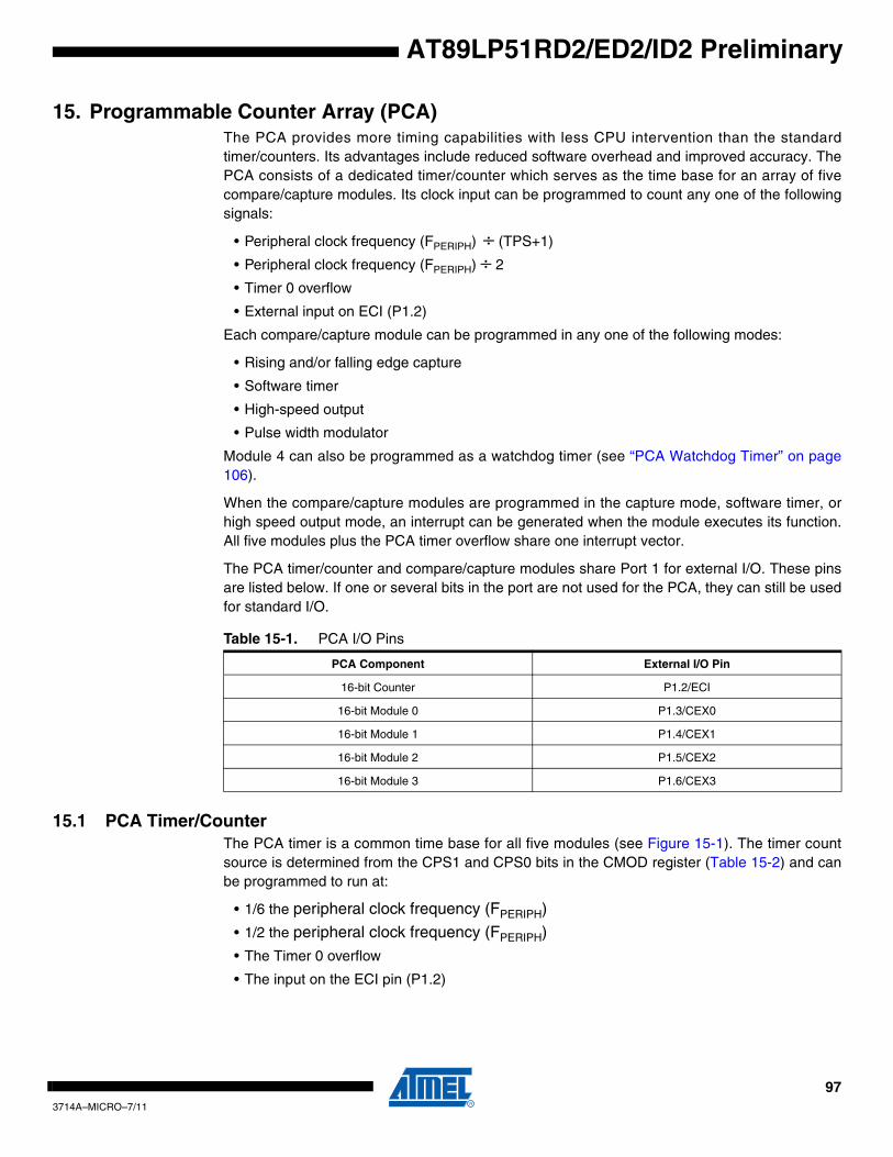
AT89LP51RD2/ED2/ID2 Preliminary
15. Programmable Counter Array (PCA)The PCA provides more timing capabilities with less CPU intervention than the standardtimer/counters. Its advantages include reduced software overhead and improved accuracy. ThePCA consists of a dedicated timer/counter which serves as the time base for an array of fivecompare/capture modules. Its clock input can be programmed to count any one of the followingsignals:
• Peripheral clock frequency (FPERIPH) ÷ (TPS+1)
• Peripheral clock frequency (FPERIPH) ÷ 2
• Timer 0 overflow
• External input on ECI (P1.2)
Each compare/capture module can be programmed in any one of the following modes:
• Rising and/or falling edge capture
• Software timer
• High-speed output
• Pulse width modulator
Module 4 can also be programmed as a watchdog timer (see “PCA Watchdog Timer” on page106).
When the compare/capture modules are programmed in the capture mode, software timer, orhigh speed output mode, an interrupt can be generated when the module executes its function.All five modules plus the PCA timer overflow share one interrupt vector.
The PCA timer/counter and compare/capture modules share Port 1 for external I/O. These pinsare listed below. If one or several bits in the port are not used for the PCA, they can still be usedfor standard I/O.
15.1 PCA Timer/CounterThe PCA timer is a common time base for all five modules (see Figure 15-1). The timer countsource is determined from the CPS1 and CPS0 bits in the CMOD register (Table 15-2) and canbe programmed to run at:
• 1/6 the peripheral clock frequency (FPERIPH)
• 1/2 the peripheral clock frequency (FPERIPH)
• The Timer 0 overflow
• The input on the ECI pin (P1.2)
Table 15-1. PCA I/O Pins
PCA Component External I/O Pin
16-bit Counter P1.2/ECI
16-bit Module 0 P1.3/CEX0
16-bit Module 1 P1.4/CEX1
16-bit Module 2 P1.5/CEX2
16-bit Module 3 P1.6/CEX3
973714A–MICRO–7/11
The CMOD register includes three additional bits associated with the PCA (See Figure 15-1 andTable 15-2).
• The CIDL bit which allows the PCA to stop during idle mode.
• The WDTE bit which enables or disables the watchdog function on module 4. (See Figure 15-4 and Section 15.7)
• The ECF bit which when set causes an interrupt and the PCA overflow flag CF (in the CCON SFR) to be set when the PCA timer overflows.
Figure 15-1. PCA Timer/Counter
The CCON register contains the run control bit for the PCA and the flags for the PCA timer (CF)and each module (Refer to Table 15-3).
• Bit CR (CCON.6) must be set by software to run the PCA. The PCA is shut off by clearing this bit.
CL CH Interrupt
CCAPnL CCAPnH
0123
fPERIPH÷(TPS+1)
Timer 0 Overflow(P1.2) ECI
CR
CF
ECF
CPS1-0
fPERIPH÷2
IdleCIDL
Overflow
To PCAModules
Table 15-2. CMOD – PCA Counter Mode Register
CMOD Address = 0D9H Reset Value = 00xx x000B
Not Bit Addressable
CIDL WDTE – – – CPS1 CPS0 ECF
Bit 7 6 5 4 3 2 1 0
Symbol Function
CIDLCounter Idle ControlClear to allow the PCA Counter to function during Idle Mode. Set to halt the PCA Counter during Idle.
WDTEWatchdog Timer EnableClear to disable the watchdog timer function on PCA Module 4. Set to enable the watchdog function of PCA Module 4.
CPS1-0
PCA Count Pulse Select
CPS1 CPS0 PCA Clock Input
0 0 fPERIPH/(TPS+1) *Note: In Fast Mode TPS is only active when PCAX2 = 1 in CKCON0.
0 1 fPERIPH/2
1 0 Timer 0 Overflow
1 1 ECI Input (P1.2)
ECFPCA Enable Counter Overflow InterruptClear to prevent the CF bit in CCON from generating an interrupt. Set to enable CF in CCON as an interrupt source.
983714A–MICRO–7/11
AT89LP51RD2/ED2/ID2 Preliminary
AT89LP51RD2/ED2/ID2 Preliminary
• Bit CF: The CF bit (CCON.7) is set when the PCA counter overflows and an interrupt will be generated if the ECF bit in the CMOD register is set. The CF bit can only be cleared by software.
• Bits 0 through 4 are the flags for the modules (bit 0 for module 0, bit 1 for module 1, etc.) and are set by hardware when either a match or a capture occurs. These flags also can only be cleared by software. The PCA interrupt system is shown in Figure 15-2.
Table 15-3. CCON – PCA Counter Control Register
CCON Address = 0D8H Reset Value = 00x0 0000B
Bit Addressable
CF CR – CCF4 CCF3 CCF2 CCF1 CCF0
Bit 7 6 5 4 3 2 1 0
Symbol Function
CFPCA Counter Overflow FlagSet by hardware when the PCA counter overflows from FFFFH to 0000H. CF generates an interrupt if the ECF bit in CMOD and EC bit in IEN0 are both set. Must be cleared by software.
CRPCA Counter Run ControlClear to disable the PCA Counter from operating. Set to enable the PCA Counter to count at the CPS rate in CMOD.
CCF4PCA Module 4 Interrupt FlagSet by hardware when a compare of match occurs in Module 4. CCF4 generates an interrupt if the ECCF4 bit in CCAPM4 and EC bit in IEN0 are both set. Must be cleared by software.
CCF3PCA Module 3 Interrupt FlagSet by hardware when a compare of match occurs in Module 2. CCF3 generates an interrupt if the ECCF3 bit in CCAPM3 and EC bit in IEN0 are both set. Must be cleared by software.
CCF2PCA Module 2 Interrupt FlagSet by hardware when a compare of match occurs in Module 2. CCF2 generates an interrupt if the ECCF2 bit in CCAPM2 and EC bit in IEN0 are both set. Must be cleared by software.
CCF1PCA Module 1 Interrupt FlagSet by hardware when a compare of match occurs in Module 1. CCF1 generates an interrupt if the ECCF1 bit in CCAPM1 and EC bit in IEN0 are both set. Must be cleared by software.
CCF0PCA Module 0 Interrupt FlagSet by hardware when a compare of match occurs in Module 0. CCF0 generates an interrupt if the ECCF0 bit in CCAPM0 and EC bit in IEN0 are both set. Must be cleared by software.
Table 15-4. CH – PCA Counter Register High
CH Address = 0F9H Reset Value = 0000 0000B
Not Bit Addressable
C15 C14 C13 C12 C11 C10 C9 C8
Bit 7 6 5 4 3 2 1 0
Symbol Function
C15-8Module n Compare/Capture Register HighHolds the higher order bits of the 16-bit PCA Timer/Counter.
993714A–MICRO–7/11
Figure 15-2. PCA Interrupt System
15.2 PCA ModulesEach one of the five compare/capture modules has six possible functions. It can perform:
• 16-bit Capture, positive-edge triggered
• 16-bit Capture, negative-edge triggered
• 16-bit Capture, both positive and negative-edge triggered
• 16-bit Software Timer
• 16-bit High Speed Output
• 8-bit Pulse Width Modulator
In addition, Module 4 can be used as a Watchdog Timer.
Each module in the PCA has a special function register associated with it. These registers are:CCAPM0 for Module 0, CCAPM1 for Module 1, etc. (See Table 15-6). The registers contain thebits that control the mode that each module will operate in.
• The ECCF bit (CCAPMn.0 where n = 0, 1, 2, 3, or 4 depending on the module) enables the CCF flag in the CCON SFR to generate an interrupt when a match or compare occurs in the associated module.
• PWM (CCAPMn.1) enables the pulse width modulation mode.
Table 15-5. CL – PCA Counter Register Low
CL Address = 0E9H Reset Value = 0000 0000B
Not Bit Addressable
C7 C6 C5 C4 C3 C2 C1 C0
Bit 7 6 5 4 3 2 1 0
Symbol Function
C7-0Module n Compare/Capture Register LowHolds the lower order bits of the 16-bit PCA Timer/Counter.
EC EA
CCF0
ECF
ECCF0
ECCF1
ECCF2
ECCF3
ECCF4
CCF0
CCF0
CCF0
CCF0
CF
0
1
2
3
4
7
CCON
Timer/Counter
Module 4
Module 3
Module 2
Module 1
Module 0
IEN0.6 IEN0.7
PCA Interruptto priority decoder
CMOD.0
CCAPMn.0
1003714A–MICRO–7/11
AT89LP51RD2/ED2/ID2 Preliminary
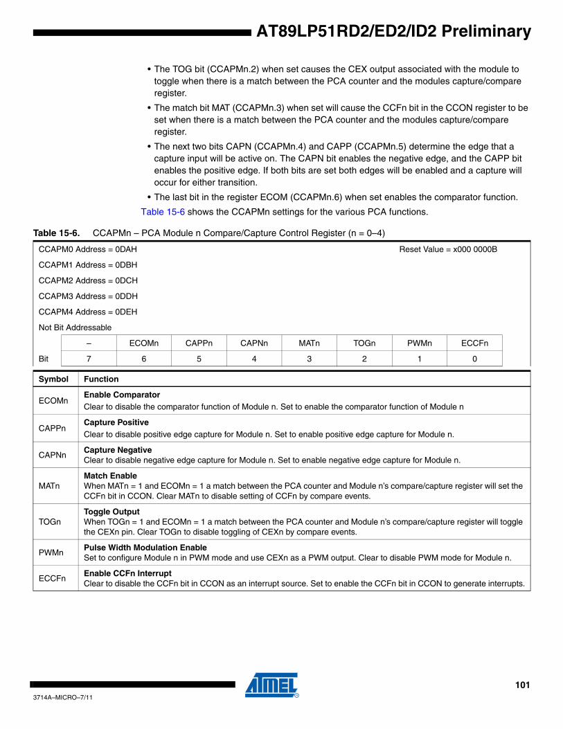
AT89LP51RD2/ED2/ID2 Preliminary
• The TOG bit (CCAPMn.2) when set causes the CEX output associated with the module to toggle when there is a match between the PCA counter and the modules capture/compare register.
• The match bit MAT (CCAPMn.3) when set will cause the CCFn bit in the CCON register to be set when there is a match between the PCA counter and the modules capture/compare register.
• The next two bits CAPN (CCAPMn.4) and CAPP (CCAPMn.5) determine the edge that a capture input will be active on. The CAPN bit enables the negative edge, and the CAPP bit enables the positive edge. If both bits are set both edges will be enabled and a capture will occur for either transition.
• The last bit in the register ECOM (CCAPMn.6) when set enables the comparator function.
Table 15-6 shows the CCAPMn settings for the various PCA functions.
Table 15-6. CCAPMn – PCA Module n Compare/Capture Control Register (n = 0–4)
CCAPM0 Address = 0DAH Reset Value = x000 0000B
CCAPM1 Address = 0DBH
CCAPM2 Address = 0DCH
CCAPM3 Address = 0DDH
CCAPM4 Address = 0DEH
Not Bit Addressable
– ECOMn CAPPn CAPNn MATn TOGn PWMn ECCFn
Bit 7 6 5 4 3 2 1 0
Symbol Function
ECOMnEnable ComparatorClear to disable the comparator function of Module n. Set to enable the comparator function of Module n
CAPPnCapture PositiveClear to disable positive edge capture for Module n. Set to enable positive edge capture for Module n.
CAPNnCapture NegativeClear to disable negative edge capture for Module n. Set to enable negative edge capture for Module n.
MATnMatch EnableWhen MATn = 1 and ECOMn = 1 a match between the PCA counter and Module n’s compare/capture register will set the CCFn bit in CCON. Clear MATn to disable setting of CCFn by compare events.
TOGnToggle OutputWhen TOGn = 1 and ECOMn = 1 a match between the PCA counter and Module n’s compare/capture register will toggle the CEXn pin. Clear TOGn to disable toggling of CEXn by compare events.
PWMnPulse Width Modulation EnableSet to configure Module n in PWM mode and use CEXn as a PWM output. Clear to disable PWM mode for Module n.
ECCFnEnable CCFn InterruptClear to disable the CCFn bit in CCON as an interrupt source. Set to enable the CCFn bit in CCON to generate interrupts.
1013714A–MICRO–7/11

There are two additional registers associated with each of the PCA modules. They are CCAPnH and CCAPnL and theseare the registers that store the 16-bit count when a capture occurs or a compare should occur. When a module is used inthe PWM mode these registers are used to control the duty cycle of the output (See Table 15-7 & Table 15-8).
Note: PCA Module Modes (CCAPMn Registers
ECOMn CAPPn CAPNn MATn TOGn PWMn ECCFn Module Function
0 0 0 0 0 0 0 No Operation
X 1 0 0 0 0 X 16-bit capture by a positive-edge trigger on CEXn
X 0 1 0 0 0 X 16-bit capture by a negative trigger on CEXn
X 1 1 0 0 0 X 16-bit capture by a transition on CEXn
1 0 0 1 0 0 X 16-bit Software Timer/Compare mode.
1 0 0 1 1 0 X 16-bit High Speed Output
1 0 0 0 0 1 0 8-bit PWM
1 0 0 1 X 0 X Watchdog Timer (module 4 only)
Table 15-7. CCAPnH – PCA Module n Compare/Capture Register High (n = 0–4)
CCAP0H Address = 0FAH Reset Value = 0000 0000B
CCAP1H Address = 0FBH
CCAP2H Address = 0FCH
CCAP3H Address = 0FDH
CCAP4H Address = 0FEH
Not Bit Addressable
CCAPn.15 CCAPn.14 CCAPn.13 CCAPn.12 CCAPn.11 CCAPn.10 CCAPn.9 CCAPn.8
Bit 7 6 5 4 3 2 1 0
Symbol Function
CCAPn15-8Module n Compare/Capture Register HighHolds the higher order bits of the 16-bit Compare/Capture value for Module n.
Table 15-8. CCAPnL – PCA Module n Compare/Capture Register Low (n = 0–4)
CCAP0L Address = 0EAH Reset Value = 0000 0000B
CCAP1L Address = 0EBH
CCAP2L Address = 0ECH
CCAP3L Address = 0EDH
CCAP4L Address = 0EEH
Not Bit Addressable
CCAPn.7 CCAPn.6 CCAPn.5 CCAPn.4 CCAPn.3 CCAPn.2 CCAPn.1 CCAPn.0
Bit 7 6 5 4 3 2 1 0
Symbol Function
CCAPn7-0Module n Compare/Capture Register LowHolds the lower order bits of the 16-bit Compare/Capture value for Module n.
1023714A–MICRO–7/11
AT89LP51RD2/ED2/ID2 Preliminary
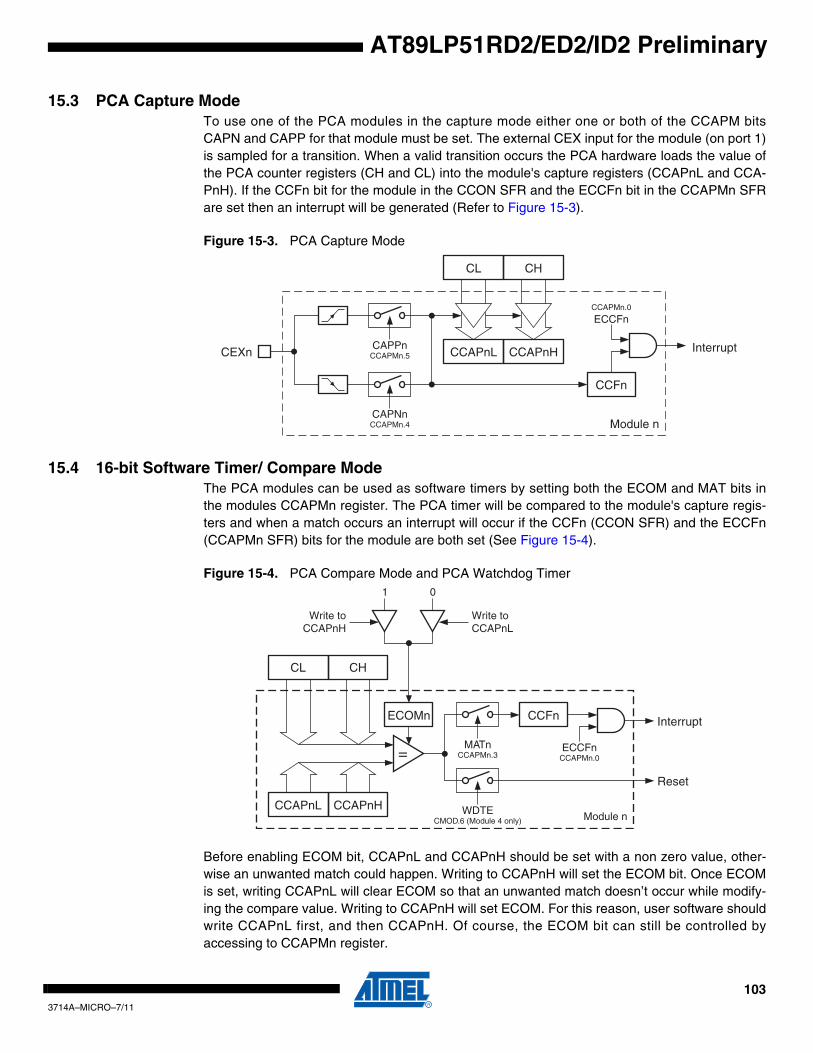
AT89LP51RD2/ED2/ID2 Preliminary
15.3 PCA Capture ModeTo use one of the PCA modules in the capture mode either one or both of the CCAPM bitsCAPN and CAPP for that module must be set. The external CEX input for the module (on port 1)is sampled for a transition. When a valid transition occurs the PCA hardware loads the value ofthe PCA counter registers (CH and CL) into the module's capture registers (CCAPnL and CCA-PnH). If the CCFn bit for the module in the CCON SFR and the ECCFn bit in the CCAPMn SFRare set then an interrupt will be generated (Refer to Figure 15-3).
Figure 15-3. PCA Capture Mode
15.4 16-bit Software Timer/ Compare ModeThe PCA modules can be used as software timers by setting both the ECOM and MAT bits inthe modules CCAPMn register. The PCA timer will be compared to the module's capture regis-ters and when a match occurs an interrupt will occur if the CCFn (CCON SFR) and the ECCFn(CCAPMn SFR) bits for the module are both set (See Figure 15-4).
Figure 15-4. PCA Compare Mode and PCA Watchdog Timer
Before enabling ECOM bit, CCAPnL and CCAPnH should be set with a non zero value, other-wise an unwanted match could happen. Writing to CCAPnH will set the ECOM bit. Once ECOMis set, writing CCAPnL will clear ECOM so that an unwanted match doesn’t occur while modify-ing the compare value. Writing to CCAPnH will set ECOM. For this reason, user software shouldwrite CCAPnL first, and then CCAPnH. Of course, the ECOM bit can still be controlled byaccessing to CCAPMn register.
CL CH
CCAPnL CCAPnH InterruptCEXn
CCFn
CCAPMn.0
ECCFn
CAPNnCCAPMn.4
CAPPnCCAPMn.5
Module n
CL CH
CCAPnL CCAPnH
InterruptCCFn
= MATn
CCAPMn.3
ECOMn
01
Write toCCAPnH
Write toCCAPnL
ECCFnCCAPMn.0
WDTECMOD.6 (Module 4 only) Module n
Reset
1033714A–MICRO–7/11

15.5 High Speed Output ModeIn this mode the CEX output (on port 1) associated with the PCA module will toggle each time amatch occurs between the PCA counter and the modules capture registers as shown in Figure15-6. To activate this mode the TOG, MAT, and ECOM bits in the module's CCAPMn SFR mustbe set (See Figure 15-5).
A prior write must be done to CCAPnL and CCAPnH before writing the ECOMn bit.
Figure 15-5. PCA High Speed Output Mode
Before enabling ECOM bit, CCAPnL and CCAPnH should be set with a non zero value, other-wise an unwanted match could happen. Once ECOM is set, writing CCAPnL will clear ECOM sothat an unwanted match doesn’t occur while modifying the compare value. Writing to CCAPnHwill set ECOM. For this reason, user software should write CCAPnL first, and then CCAPnH. Ofcourse, the ECOM bit can still be controlled by accessing to CCAPMn register.
An example of a High Speed Output waveform is shown in Figure 15-6. The frequency of theoutput can be controlled by reloading the PCA Timer in software and/or changing the comparevalues multiple times per timeout period.
Figure 15-6. High Speed Output Waveform
CL CH
CCAPnL CCAPnH
InterruptCCFn
= MATn
CCAPMn.3
ECOMn
01
Write toCCAPnH
Write toCCAPnL
ECCFnCCAPMn.0
TOGnCCAPMn.2 Module n
CEXn
{CH,CL} = FFFFH
TOGn = 1, ECOMn = 1
CEXn
{CCAPnH,CCAPnL}
{CH,CL} = 0000H
1043714A–MICRO–7/11
AT89LP51RD2/ED2/ID2 Preliminary
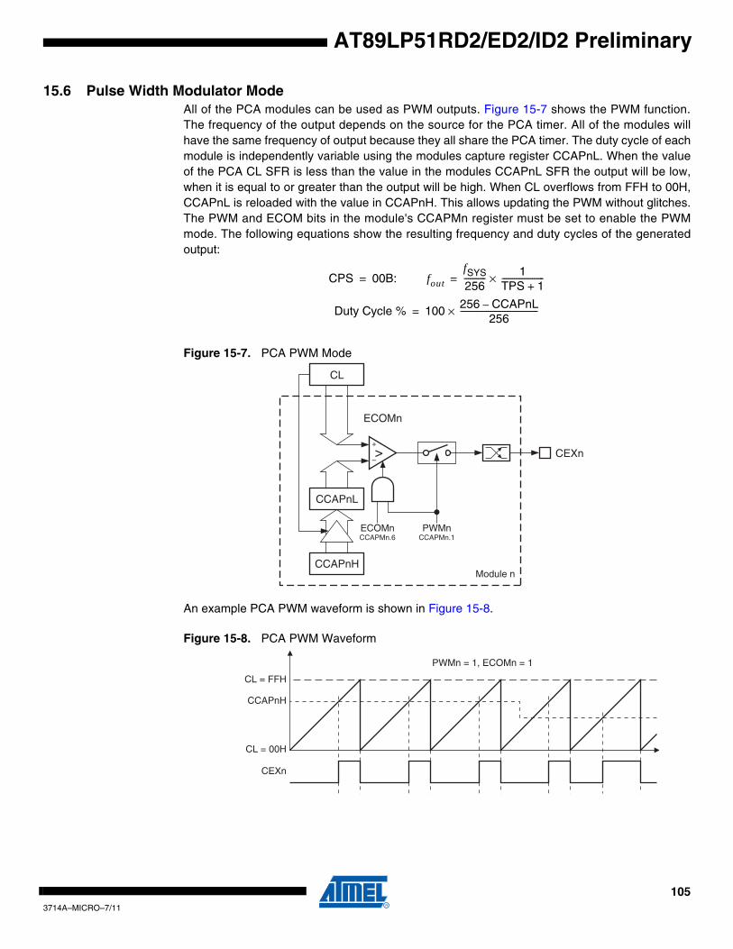
AT89LP51RD2/ED2/ID2 Preliminary
15.6 Pulse Width Modulator ModeAll of the PCA modules can be used as PWM outputs. Figure 15-7 shows the PWM function.The frequency of the output depends on the source for the PCA timer. All of the modules willhave the same frequency of output because they all share the PCA timer. The duty cycle of eachmodule is independently variable using the modules capture register CCAPnL. When the valueof the PCA CL SFR is less than the value in the modules CCAPnL SFR the output will be low,when it is equal to or greater than the output will be high. When CL overflows from FFH to 00H,CCAPnL is reloaded with the value in CCAPnH. This allows updating the PWM without glitches.The PWM and ECOM bits in the module's CCAPMn register must be set to enable the PWMmode. The following equations show the resulting frequency and duty cycles of the generatedoutput:
Figure 15-7. PCA PWM Mode
An example PCA PWM waveform is shown in Figure 15-8.
Figure 15-8. PCA PWM Waveform
CPS 00B:= foutfSYS
256----------- 1
TPS 1+---------------------×=
Duty Cycle % 100256 CCAPnL–
256---------------------------------------×=
CL
CCAPnH
CCAPnL
>
ECOMn
PWMnCCAPMn.1
Module n
CEXn+
–
ECOMnCCAPMn.6
CL = FFH
PWMn = 1, ECOMn = 1
CCAPnH
CEXn
CL = 00H
1053714A–MICRO–7/11
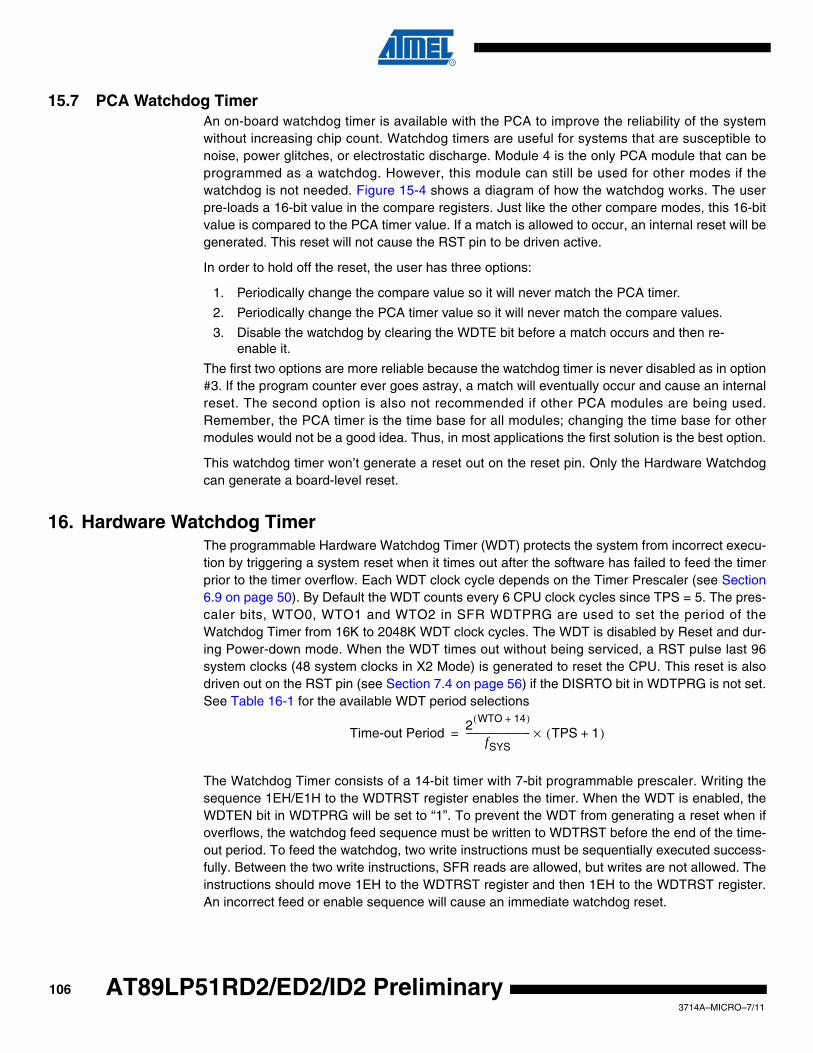
15.7 PCA Watchdog Timer An on-board watchdog timer is available with the PCA to improve the reliability of the systemwithout increasing chip count. Watchdog timers are useful for systems that are susceptible tonoise, power glitches, or electrostatic discharge. Module 4 is the only PCA module that can beprogrammed as a watchdog. However, this module can still be used for other modes if thewatchdog is not needed. Figure 15-4 shows a diagram of how the watchdog works. The userpre-loads a 16-bit value in the compare registers. Just like the other compare modes, this 16-bitvalue is compared to the PCA timer value. If a match is allowed to occur, an internal reset will begenerated. This reset will not cause the RST pin to be driven active.
In order to hold off the reset, the user has three options:
1. Periodically change the compare value so it will never match the PCA timer.
2. Periodically change the PCA timer value so it will never match the compare values.
3. Disable the watchdog by clearing the WDTE bit before a match occurs and then re-enable it.
The first two options are more reliable because the watchdog timer is never disabled as in option#3. If the program counter ever goes astray, a match will eventually occur and cause an internalreset. The second option is also not recommended if other PCA modules are being used.Remember, the PCA timer is the time base for all modules; changing the time base for othermodules would not be a good idea. Thus, in most applications the first solution is the best option.
This watchdog timer won’t generate a reset out on the reset pin. Only the Hardware Watchdogcan generate a board-level reset.
16. Hardware Watchdog TimerThe programmable Hardware Watchdog Timer (WDT) protects the system from incorrect execu-tion by triggering a system reset when it times out after the software has failed to feed the timerprior to the timer overflow. Each WDT clock cycle depends on the Timer Prescaler (see Section6.9 on page 50). By Default the WDT counts every 6 CPU clock cycles since TPS = 5. The pres-caler bits, WTO0, WTO1 and WTO2 in SFR WDTPRG are used to set the period of theWatchdog Timer from 16K to 2048K WDT clock cycles. The WDT is disabled by Reset and dur-ing Power-down mode. When the WDT times out without being serviced, a RST pulse last 96system clocks (48 system clocks in X2 Mode) is generated to reset the CPU. This reset is alsodriven out on the RST pin (see Section 7.4 on page 56) if the DISRTO bit in WDTPRG is not set.See Table 16-1 for the available WDT period selections
The Watchdog Timer consists of a 14-bit timer with 7-bit programmable prescaler. Writing thesequence 1EH/E1H to the WDTRST register enables the timer. When the WDT is enabled, theWDTEN bit in WDTPRG will be set to “1”. To prevent the WDT from generating a reset when ifoverflows, the watchdog feed sequence must be written to WDTRST before the end of the time-out period. To feed the watchdog, two write instructions must be sequentially executed success-fully. Between the two write instructions, SFR reads are allowed, but writes are not allowed. Theinstructions should move 1EH to the WDTRST register and then 1EH to the WDTRST register.An incorrect feed or enable sequence will cause an immediate watchdog reset.
Time-out Period2
WTO 14+( )
fSYS----------------------------- TPS 1+( )×=
1063714A–MICRO–7/11
AT89LP51RD2/ED2/ID2 Preliminary

AT89LP51RD2/ED2/ID2 Preliminary
The program sequence to feed or enable the watchdog timer is as follows:
MOV WDTRST, #01EhMOV WDTRST, #0E1h
The WDT time-out period is dependent on the system clock frequency.
16.1 Software ResetA Software Reset of the AT89LP51RD2/ED2/ID2 is accomplished by writing the software resetsequence 5AH/A5H to the WDTRST SFR. The WDT does not need to be enabled to generatethe software reset. A normal software reset will set the SWRST flag in WDTCON. However, if atany time an incorrect sequence is written to WDTRST (i.e. anything other than 1EH/E1H or5AH/A5H), a software reset will immediately be generated and both the SWRST and WDTOVFflags will be set. In this manner an intentional software reset may be distinguished from a soft-ware error-generated reset. The program sequence to generate a software reset is as follows:
MOV WDTRST, #05AhMOV WDTRST, #0A5h
A software reset has the same duration as the normal watchdog reset and will also generate areset pulse on the RST pin unless DISRTO is set.
Table 16-1. Watchdog Timer Time-out Period Selection
WDT Prescaler BitsPeriod()
(Clock Cycles)WTO2 WTO1 WTO0
0 0 0 16K x (TPS+1)
0 0 1 32K x (TPS+1)
0 1 0 64K x (TPS+1)
0 1 1 128K x (TPS+1)
1 0 0 256K x (TPS+1)
1 0 1 512K x (TPS+1)
1 1 0 1024K x (TPS+1)
1 1 1 2048K x (TPS+1)
1073714A–MICRO–7/11

16.2 WDT Registers)
Table 16-2. WDTPRG – Watchdog Control Register
WDTPRG Address = A7H Reset Value = xx00 0000B
Not Bit Addressable
WDTOVF SWRST WDTEN WDIDLE DISRTO WTO2 WTO1 WTO0
Bit 7 6 5 4 3 2 1 0
Symbol Function
WDTOVFWatchdog Overflow FlagSet by hardware when a WDT rest is generated by the WDT timer overflow. Also set when an incorrect sequence is written to WDTRST. Must be cleared by software.
SWRSTSoftware Reset FlagSet by hardware when a software reset is generated by writing the sequence 5AH/A5H to WDTRST. Also set when an incorrect sequence is written to WDTRST. Must be cleared by software.
WDTENWatchdog Enable FlagThis bit is READ-ONLY and reflects the status of the WDT (whether it is running or not). The WDT is disabled after any reset and must be re-enabled by writing 1EH/E1H to WDTRST
WDIDLEWDT Disable During IdleWhen WDIDLE = 0 the WDT continues to count in Idle mode. When WDIDLE = 1 the WDT halts counting in Idle mode.
DISRTODisable Reset OutputWhen DISTRO = 0 the reset pin is driven to the same level as POL when the WDT resets. When DISRTO = 1 the reset pin is input only.
WTO2WTO1WTO0
Watchdog TiemoutPrescaler bits for the watchdog timer (WDT). When all three bits are cleared to 0, the watchdog timer has a nominal period of 16K clock cycles. When all three bits are set to 1, the nominal period is 2048K clock cycles.
Table 16-3. WDTRST – Watchdog Reset Register
WDTCON Address = A6H (Write-Only)
Not Bit Addressable
– – – – – – – –
Bit 7 6 5 4 3 2 1 0
The WDT is enabled by writing the sequence 1EH/E1H to the WDTRST SFR. The current status may be checked by reading the WDTEN bit in WDTCON. To prevent the WDT from resetting the device, the same sequence 1EH/E1H must be written to WDTRST before the time-out interval expires. A software reset is generated by writing the sequence 5AH/A5H to WDTRST.
1083714A–MICRO–7/11
AT89LP51RD2/ED2/ID2 Preliminary
AT89LP51RD2/ED2/ID2 Preliminary
17. Serial Interface (UART)The serial interface on the AT89LP51RD2/ED2/ID2 implements a Universal AsynchronousReceiver/Transmitter (UART). The UART has the following features:
• Full-duplex Operation
• 8 or 9 Data Bits
• Framing Error Detection
• Multiprocessor Communication Mode with Automatic Address Recognition
• Baud Rate Generator Using Timer 1, Timer 2 or dedicated Internal Baud Rate Generator
• Interrupt on Receive Buffer Full or Transmission Complete
• Synchronous SPI or TWI Master Emulation
The serial interface is full-duplex, which means it can transmit and receive simultaneously. It isalso receive-buffered, which means it can begin receiving a second byte before a previouslyreceived byte has been read from the receive register. (However, if the first byte still has notbeen read when reception of the second byte is complete, one of the bytes will be lost.) Theserial port receive and transmit registers are both accessed at the Special Function RegisterSBUF. Writing to SBUF loads the transmit register, and reading SBUF accesses a physicallyseparate receive register. The serial port can operate in the following four modes.
• Mode 0: Serial data enters and exits through RXD. TXD outputs the shift clock. Eight data bits are transmitted/received, with the LSB first. The baud rate is programmable to 1/6 or 1/3 the system frequency in Compatibility mode, 1/4 or 1/2 the system frequency in Fast mode, or variable based on Time 1.
• Mode 1: 10 bits are transmitted (through TXD) or received (through RXD): a start bit (0), 8 data bits (LSB first), and a stop bit (1). On receive, the stop bit goes into RB8 in the Special Function Register SCON. The baud rate is variable based on Timer 1 or Timer 2.
• Mode 2: 11 bits are transmitted (through TXD) or received (through RXD): a start bit (0), 8 data bits (LSB first), a programmable 9th data bit, and a stop bit (1). On transmit, the 9th data bit (TB8 in SCON) can be assigned the value of “0” or “1”. For example, the parity bit (P, in the PSW) can be moved into TB8. On receive, the 9th data bit goes into RB8 in the Special Function Register SCON, while the stop bit is ignored. The baud rate is programmable to either 1/16 or 1/32 the system frequency.
• Mode 3: 11 bits are transmitted (through TXD) or received (through RXD): a start bit (0), 8 data bits (LSB first), a programmable 9th data bit, and a stop bit (1). In fact, Mode 3 is the same as Mode 2 in all respects except the baud rate, which is variable based on Timer 1 or Timer 2 in Mode 3.
In all four modes, transmission is initiated by any instruction that uses SBUF as a destinationregister. Reception is initiated in Mode 0 by the condition RI = 0 and REN = 1. Reception is initi-ated in the other modes by the incoming start bit if REN = 1.
1093714A–MICRO–7/11

Notes: 1. SMOD0 is located at PCON.6.2. fSYS = system frequency. The baud rate depends on SMOD1 (PCON.7).
Table 17-1. SCON – Serial Port Control Register
SCON Address = 98H Reset Value = 0000 0000B
Bit Addressable
SM0/FE SM1 SM2 REN TB8 RB8 T1 RI
Bit 7 6 5 4 3 2 1 0
(SMOD0 = 0/1)(1)
Symbol Function
FE
Framing Error BitThis bit is set by the receiver when an invalid stop bit is detected. The FE bit is not cleared by valid frames and must be cleared by software. The SMOD0 bit must be set to enable access to the FE bit. FE will be set regardless of the state of SMOD0.
SM0Serial Port Mode Bit 0Refer to SM1 for serial port mode selection. SMOD0 must = 0 to access bit SM0.
SM1
Serial Port Mode Bit 1
SM2
Multiprocessor Communications EnableEnables the Automatic Address Recognition feature in Modes 2 or 3. If SM2 = 1 then Rl will not be set unless the received 9th data bit (RB8) is 1, indicating an address, and the received byte is a Given or Broadcast Address. In Mode 1, if SM2 = 1 then Rl will not be activated unless a valid stop bit was received, and the received byte is a Given or Broadcast Address. In Mode 0, SM2 determines the idle state of the shift clock such that the clock is the inverse of SM2, i.e. when SM2 = 0 the clock idles high and when SM2 = 1 the clock idles low.
RENSerial Reception EnableSet by software to enable reception. Clear by software to disable reception.
TB8Transmitter Bit 8The 9th data bit that will be transmitted in Modes 2 and 3. Set or clear by software as desired. In Mode 0, setting TB8 enables Timer 1 as the shift clock generator.
RB8Receiver Bit 8In Modes 2 and 3, the 9th data bit that was received. In Mode 1, if SM2 = 0, RB8 is the stop bit that was received. In Mode 0, RB8 is not used.
TITransmit Interrupt FlagSet by hardware at the end of the 8th bit time in Mode 0, or at the beginning of the stop bit in the other modes, in any serial transmission. Must be cleared by software.
RIReceive Interrupt FlagSet by hardware at the end of the 8th bit time in Mode 0, or halfway through the stop bit time in the other modes, in any serial reception (except see SM2). Must be cleared by software.
SM0 SM1 Mode Description Baud Rate (Compat.)(2) Baud Rate (Fast)(2)
0 0 0 shift register fSYS/3 or fSYS/6 or Timer 1 fSYS/2 or fSYS/4 or Timer 1
0 1 1 8-bit UART variable (Timer 1 or Timer 2) variable (Timer 1 or Timer 2)
1 0 2 9-bit UART fSYS/32 or fSYS/16 fSYS/32 or fSYS/16
1 1 3 9-bit UART variable (Timer 1 or Timer 2) variable (Timer 1 or Timer 2)
1103714A–MICRO–7/11
AT89LP51RD2/ED2/ID2 Preliminary

AT89LP51RD2/ED2/ID2 Preliminary
17.1 Multiprocessor CommunicationsModes 2 and 3 have a special provision for multiprocessor communications. In these modes,9 data bits are received, followed by a stop bit. The 9th bit goes into RB8. Then comes a stop bit.The port can be programmed such that when the stop bit is received, the serial port interrupt isactivated only if RB8 = 1. This feature is enabled by setting bit SM2 in SCON.
The following example shows how to use the serial interrupt for multiprocessor communications.When the master processor must transmit a block of data to one of several slaves, it first sendsout an address byte that identifies the target slave. An address byte differs from a data byte inthat the 9th bit is “1” in an address byte and “0” in a data byte. With SM2 = 1, no slave isinterrupted by a data byte. An address byte, however, interrupts all slaves. Each slave canexamine the received byte and see if it is being addressed. The addressed slave clears its SM2bit and prepares to receive the data bytes that follows. The slaves that are not addressed settheir SM2 bits and ignore the data bytes. See “Automatic Address Recognition” on page 116.
The SM2 bit can be used to check the validity of the stop bit in Mode 1. In a Mode 1 reception, ifSM2 = 1, the receive interrupt is not activated unless a valid stop bit is received.
17.2 Baud RatesThe baud rate in Mode 0 depends on the value of the SMOD1 bit in Special Function RegisterPCON.7. If SMOD1 = 0 (the value on reset) and TB8 = 0, the baud rate is 1/4 of the system fre-quency in Fast mode. If SMOD1 = 1 and TB8 = 0, the baud rate is 1/2 of the system frequency,as shown in the following equation:
In Compatibility mode the baud rate is 1/6 of the system frequency, scaling to 1/3 whenSMOD1 = 1.
Mode 0 can also be generated from either Timer 1 or the Internal Baud Rate Generator bysetting TB8 in SCON or SRC in BDRCON respectively.
The baud rate in Mode 2 also depends on the value of the SMOD1 bit. If SMOD1 = 0, the baudrate is 1/32 of the system frequency. If SMOD1 = 1, the baud rate is 1/16 of the system fre-quency, as shown in the following equation:
The baud rate in Modes 1 and 3 is generated from one of Timer 1, Timer 2 or the Internal BaudRate Generator as detailed in Table 17-2.
Mode 0 Baud Rate
TB8 = 0
2SMOD1
4-------------------- System Frequency×=
Mode 0 Baud Rate
TB8 = 0
2SMOD1
6-------------------- System Frequency×=
Mode 2 Baud Rate2
SMOD1
32-------------------- System Frequency×=
1113714A–MICRO–7/11

17.2.1 Using Timer 1 to Generate Baud RatesSetting TB8 = 1 in Mode 0 enables Timer 1 as the baud rate generator. When Timer 1 is thebaud rate generator for Mode 0, the baud rates are determined by the Timer 1 overflow rate andthe value of SMOD1 according to the following equation:
The Timer 1 overflow rate normally determines the baud rates in Modes 1 and 3. When Timer 1is the baud rate generator, the baud rates are determined by the Timer 1 overflow rate and thevalue of SMOD1 according to the following equation:
The Timer 1 interrupt should be disabled in this application. The Timer itself can be configuredfor either timer or counter operation in any of its 3 running modes. In the most typical applica-tions, it is configured for timer operation in auto-reload mode (high nibble of TMOD = 0010B). Inthis case, the baud rate is given by the following formula:
Table 17-3 lists commonly used baud rates and how they can be obtained from Timer 1.
Table 17-2. UART Baud Rate Selection Table for Modes 1 and 3
TCLK(T2CON.4)
RCLK(T2CON.5)
TBCK(BDRCON.3)
RBCK(BDRCON.2)
Clock Source UART Tx
Clock Source UART Rx
0 0 0 0 Timer 1 Timer 1
1 0 0 0 Timer 2 Timer 1
0 1 0 0 Timer 1 Timer 2
1 1 0 0 Timer 2 Timer 2
X 0 1 0 BRG Timer 1
X 1 1 0 BRG Timer 2
0 X 0 1 Timer 1 BRG
1 X 0 1 Timer 2 BRG
X X 1 1 BRG BRG
Mode 0 Baud Rate
TB8 = 1
2SMOD1
4-------------------- (Timer 1 Overflow Rate)×=
Modes 1, 3
Baud Rate
2SMOD1
32-------------------- (Timer 1 Overflow Rate)×=
Modes 1, 3
Baud Rate
2SMOD1
32-------------------- System Frequency
256 TH1( )–[ ]-------------------------------------------------- 1
TPS 1+---------------------××=
1123714A–MICRO–7/11
AT89LP51RD2/ED2/ID2 Preliminary

AT89LP51RD2/ED2/ID2 Preliminary
17.2.2 Using Timer 2 to Generate Baud RatesTimer 2 is selected as the baud rate generator by setting TCLK and/or RCLK in T2CON. Underthese conditions, the baud rates for transmit and receive can be simultaneously different byusing Timer 1 for transmit and Timer 2 for receive, or vice versa. The baud rate generator modeis similar to the auto-reload mode, in that a rollover causes the Timer 2 registers to be reloadedwith the 16-bit value in registers RCAP2H and RCAP2L, which are preset by software. In thiscase, the baud rates in Modes 1 and 3 are determined by Timer 2’s overflow rate according tothe following equation:
Table 17-4 lists commonly used baud rates and how they can be obtained from Timer 2. Notethat TPS and T2X2 do not apply to Timer 2 in baud rate mode.
Table 17-3. Commonly Used Baud Rates Generated by Timer 1
Baud Rate fOSC (MHz) X2 SMOD1
Timer 1
C/T Mode TPS Reload Value
Mode 0 Max: 6 MHz 12 1 1 X X 0 X
Mode 2 Max: 750K 12 1 1 X X 0 X
Modes 1, 3 Max: 750K 12 1 1 0 2 0 F4H
19.2K 11.059 1 1 0 2 0 DCH
9.6K 11.059 1 0 0 2 0 DCH
4.8K 11.059 1 0 0 2 0 B8H
2.4K 11.059 1 0 0 2 0 70H
1.2K 11.059 1 0 0 1 0 FEE0H
137.5 11.986 1 0 0 1 0 F55CH
110 6 1 1 0 1 0 F2AFH
110 12 1 0 0 1 0 F2AFH
19.2K 11.059 0 1 0 2 5 FDH
9.6K 11.059 0 0 0 2 5 FDH
4.8K 11.059 0 0 0 2 5 FAH
2.4K 11.059 0 0 0 2 5 F4H
1.2K 11.059 0 0 0 2 5 E8H
137.5 11.986 0 0 0 2 5 1DH
110 6 0 0 0 2 5 72H
110 12 0 0 0 1 5 FEEBH
Modes 1 and 3
Baud Rate
116------ System Frequency
65536 RCAP2H,RCAP2L( )–[ ]---------------------------------------------------------------------------------×=
1133714A–MICRO–7/11

17.2.3 Internal Baud Rate Generator (BRG)The AT89LP51RD2/ED2/ID2 includes an Internal Baud Rate Generator (BRG) for UART modes1 and 3 that can free up Timer 1 or Timer 2 for other uses. The BRG is an 8-bit counter withreload as shown in Figure 17-1. On overflow, the BRG is loaded with the value of BRL. The BRGis controlled by the BDRCON register (See Table 17-7). The BRG operates when BRR = 1. TheSPD bit determines the clock source: either the system clock divided-by-6 or the system clockwith no division. The BRG is not affected by the Timer Prescaler; however, it is affected by theSMOD1 bit in PCON. The following equation shows the baud rate calculation using the BRG:
The output of the Internal Baud Rate Generator can be independently selected for the transmitand receive clocks using the TBCK and RBCK bits in BDRCON. These bits have priority overthe TCLK and TCLK bits in T2CON as shown in Table 17-2. Table 17-5 lists some commonbaud rates generated by the BRG.
Table 17-4. Commonly Used Baud Rates Generated by Timer 2
Baud Rate fOSC (MHz) X2
Timer 2
CP/RL2 C/T2 TCLK or RCLK Reload Value
Max: 750K 12 1 0 0 1 FFFFH
19.2K 11.059 1 0 0 1 FFDCH
9.6K 11.059 1 0 0 1 FFB8H
4.8K 11.059 1 0 0 1 FF70H
2.4K 11.059 1 0 0 1 FEE0H
1.2K 11.059 1 0 0 1 FDC0H
137.5 11.986 1 0 0 1 EAB8H
110 6 1 0 0 1 F2AFH
110 12 1 0 0 1 E55EH
19.2K 11.059 0 0 0 1 FFEEH
9.6K 11.059 0 0 0 1 FFDCH
4.8K 11.059 0 0 0 1 FFB8H
2.4K 11.059 0 0 0 1 FF70H
1.2K 11.059 0 0 0 1 FEE0H
137.5 11.986 0 0 0 1 F55CH
110 12 0 0 0 1 F2AFH
Baud Rate2
SMOD1
32--------------------
fSYS
256 BRL( )–-------------------------------- 1
61 SPD–( )
------------------------××=
1143714A–MICRO–7/11
AT89LP51RD2/ED2/ID2 Preliminary

AT89LP51RD2/ED2/ID2 Preliminary
Figure 17-1. Internal Baud Rate Generator
Table 17-5. Commonly Used Baud Rates Generated by BRG
Baud Rate X2 SMOD1 SPD
fOSC = 16.384 MHz fOSC = 24 MHz
BRL Error (%) BRL Error (%)
115200 1 1 1 247 1.23 243 0.16
57600 1 1 1 238 1.23 230 0.16
38400 1 1 1 229 1.23 217 0.16
28800 1 1 1 220 1.23 204 0.16
19200 1 1 1 203 0.63 178 0.16
9600 1 1 1 149 0.31 100 0.16
4800 1 1 1 43 1.23 – –
4800 0 0 0 247 1.23 243 0.16
2400 0 0 0 238 1.23 230 0.16
1200 0 0 0 220 1.23 202 3.55
600 0 0 0 185 0.16 152 0.16
BRG
BRL
UART
0
1
BRR(BDRCON.4)
CLKSYS
Overflow
SPD(BDRCON.1)
÷60
1
SMOD1(PCON.7)
÷6
Table 17-6. BRL – Baud Rate Reload Register
BRL Address = 09AH Reset Value = 0000 0000B
Not Bit Addressable
Bit 7 6 5 4 3 2 1 0
Symbol Function
BRL7-0
Baud Rate Reload ValueHolds the 8-bit reload value of the Internal Baud Rate Generator. This value is loaded into the BRG when the BRG overflows from FFH to 00H.
1153714A–MICRO–7/11

17.3 Framing Error DetectionIn addition to all of its usual modes, the UART can perform framing error detection by looking formissing stop bits. When used for framing error detect, the UART looks for missing stop bits inthe communication. A missing bit will set the FE bit in the SCON register. The FE bit shares theSCON.7 bit with SM0 and the function of SCON.7 is determined by PCON.6 (SMOD0). IfSMOD0 is set then SCON.7 functions as FE. SCON.7 functions as SM0 when SMOD0 iscleared. When used as FE, SCON.7 can only be cleared by software. The FE bit will be set by aframing error regardless of the state of SMOD0.
17.4 Automatic Address RecognitionAutomatic Address Recognition is a feature which allows the UART to recognize certainaddresses in the serial bit stream by using hardware to make the comparisons. This featuresaves a great deal of software overhead by eliminating the need for the software to examineevery serial address which passes by the serial port. This feature is enabled by setting the SM2bit in SCON for Modes 1, 2 or 3. In the 9-bit UART modes, Mode 2 and Mode 3, the ReceiveInterrupt flag (RI) will be automatically set when the received byte contains either the “Given”address or the “Broadcast” address. The 9-bit mode requires that the 9th information bit be a “1”to indicate that the received information is an address and not data.
In Mode 1 (8-bit) the RI flag will be set if SM2 is enabled and the information received has a validstop bit following the 8th address bits and the information is either a Given or Broadcastaddress. Using the Automatic Address Recognition feature allows a master to selectively com-municate with one or more slaves by invoking the given slave address or addresses. All of theslaves may be contacted by using the Broadcast address. Automatic Address Recognition is notavailable during Mode 0.
Table 17-7. BDRCON – Baud Rate Control Register
BDRCON Address = 9BH Reset Value = xxx0 0000B
Not Bit Addressable
– – – BRR TBCK RBCK SPD SRC
Bit 7 6 5 4 3 2 1 0
Symbol Function
BRRBaud Rate Run ControlClear to stop the Internal Baud Rate Generator. Set to start the Internal Baud Rate Generator.
TBCKTransmission Baud Rate SelectClear to select Timer 1 or Timer 2 overflow as transmit clock for the serial port. Set to select the Internal Baud Rate Generator as transmit clock for the serial port.
RBCKReceive Baud Rate SelectClear to select Timer 1 or Timer 2 overflow as receive clock for the serial port. Set to select the Internal Baud Rate Generator as receive clock for the serial port.
SPDBRG Speed ControlClear to select the SLOW baud rate generator mode. Set to select the FAST baud rate generator mode.
SRCBaud Rate Source for Mod e 0Clear to select fixed or Timer 1 clock source for UART mode 0. Set to select BRG for UART mode 0.
1163714A–MICRO–7/11
AT89LP51RD2/ED2/ID2 Preliminary

AT89LP51RD2/ED2/ID2 Preliminary
17.4.1 Given AddressTwo special Function Registers are used to define the slave’s address, SADDR (A9H), and theaddress mask, SADEN (B9H). SADEN is used to define which bits in the SADDR are to be usedand which bits are “don’t care”. The SADEN mask can be logically ANDed with the SADDR tocreate the “Given” address which the master will use for addressing each of the slaves. Use ofthe Given address allows multiple slaves to be recognized while excluding others. The followingexamples show the versatility of this scheme:
Slave 0 SADDR = 1100 0000SADEN = 1111 1101Given = 1100 00X0
Slave 1 SADDR = 1100 0000SADEN = 1111 1110Given = 1100 000X
In the previous example, SADDR is the same and the SADEN data is used to differentiatebetween the two slaves. Slave 0 requires a “0” in bit 0 and it ignores bit 1. Slave 1 requires a “0”in bit 1 and bit 0 is ignored. A unique address for slave 0 would be 1100 0010 since slave 1requires a “0” in bit 1. A unique address for slave 1 would be 1100 0001 since a “1” in bit 0 willexclude slave 0. Both slaves can be selected at the same time by an address which has bit 0 = 0(for slave 0) and bit 1 = 0 (for slave 1). Thus, both could be addressed with 1100 0000.
In a more complex system, the following could be used to select slaves 1 and 2 while excludingslave 0:
Slave 0 SADDR = 1100 0000SADEN = 1111 1001Given = 1100 0XX0
Slave 1 SADDR = 1110 0000SADEN = 1111 1010Given = 1110 0X0X
Slave 2 SADDR = 1110 0000SADEN = 1111 1100Given = 1110 00XX
In the above example, the differentiation among the 3 slaves is in the lower 3 address bits. Slave0 requires that bit 0 = 0 and it can be uniquely addressed by 1110 0110. Slave 1 requires thatbit 1 = 0 and it can be uniquely addressed by 1110 and 0101. Slave 2 requires that bit 2 = 0 andits unique address is 1110 0011. To select Slaves 0 and 1 and exclude Slave 2, use address1110 0100, since it is necessary to make bit 2 = 1 to exclude slave 2.
Upon reset the SADDR and SADEN registers are loaded with “0”s. This produces a givenaddress of all “don’t cares” as well as a Broadcast address of all “don’t cares”. This effectivelydisables the Automatic Addressing mode and allows the microcontroller to use standard 80C51-type UART drivers which do not make use of this feature.
1173714A–MICRO–7/11
17.4.2 Broadcast AddressThe Broadcast Address for each slave is created by taking the logic OR of SADDR and SADEN.Zeros in this result are trended as don’t cares. In most cases, interpreting the don’t cares asones, the broadcast address will be FF hexadecimal.
17.5 More About Mode 0In Mode 0, the UART is configured as a two wire half-duplex synchronous serial interface. Intwo-wire mode serial data enters and exits through RXD and TXD outputs the shift clock. Eightdata bits are transmitted/received, with the LSB first. Figure 17-4 and Figure 17.6 on page 122show simplified functional diagrams of the serial port in Mode 0 and associated timing. The baudrate is programmable to 1/2 or 1/4 the system frequency by setting/clearing the SMOD1 bit inFast mode, or 1/3 or 1/6 the system frequency in Compatibility mode. However, changingSMOD1 has an effect on the relationship between the clock and data as described below. Thebaud rate can also be generated by Timer 1 by setting TB8 in SCON or the Internal Baud RateGenerator by setting SRC in BDRCON. Table 17-10 lists the baud rate options for Mode 0.
Table 17-8. SADDR – Slave Address Register
SADDR Address = 0A9H Reset Value = 0000 0000B
Not Bit Addressable
Bit 7 6 5 4 3 2 1 0
Symbol Function
SADDR7-0
UART Slave AddressWhen SM2 = 1, SADDR holds the 8-bit address for the UART multiprocessor communication mode. This address is combined with SADEN to create the given and broadcast addresses for the device.
Table 17-9. SADEN – Slave Address Mask Register
SADEN Address = 0B9H Reset Value = 0000 0000B
Not Bit Addressable
Bit 7 6 5 4 3 2 1 0
Symbol Function
SADEN7-0
UART Slave Address MaskWhen SM2 = 1, SADEN holds the 8-bit address mask for the UART multiprocessor communication mode. This address is combined with SADDR to create the given and broadcast addresses for the device.
Table 17-10. Mode 0 Baud Rates
SRC TB8 SMOD1 Baud Rate (Fast) Baud Rate (Compatibility)
0 0 0 fSYS/4 fSYS/6
0 0 1 fSYS/2 fSYS/3
0 1 0 (Timer 1 Overflow) / 4 (Timer 1 Overflow) / 4
0 1 1 (Timer 1 Overflow) / 2 (Timer 1 Overflow) / 2
1 X 0 (BRG Overflow) / 2 (BRG Overflow) / 2
1 X 1 BRG Overflow BRG Overflow
1183714A–MICRO–7/11
AT89LP51RD2/ED2/ID2 Preliminary

AT89LP51RD2/ED2/ID2 Preliminary
17.5.1 Two-Wire (Half-Duplex) ModeTransmission is initiated by any instruction that uses SBUF as a destination register. The “writeto SBUF” signal also loads a “1” into the 9th position of the transmit shift register and tells the TXControl Block to begin a transmission. The internal timing is such that one full bit slot may elapsebetween “write to SBUF” and activation of SEND.
SEND transfers the output of the shift register to the alternate output function line of P3.0, andalso transfers Shift Clock to the alternate output function line of P3.1. As data bits shift out to theright, “0”s come in from the left. When the MSB of the data byte is at the output position of theshift register, the “1” that was initially loaded into the 9th position is just to the left of the MSB,and all positions to the left of that contain “0”s. This condition flags the TX Control block to doone last shift, then deactivate SEND and set TI.
Reception is initiated by the condition REN = 1 and RI = 0. At the next clock cycle, the RX Con-trol unit writes the bits 11111110B to the receive shift register and activates RECEIVE in thenext clock phase. RECEIVE enables Shift Clock to the alternate output function line of P3.1. Asdata bits come in from the right, “1”s shift out to the left. When the “0” that was initially loadedinto the right-most position arrives at the left-most position in the shift register, it flags the RXControl block to do one last shift and load SBUF. Then RECEIVE is cleared and RI is set.
The relationship between the shift clock and data is determined by the combination of the SM2and SMOD1 bits as listed in Table 17-11 and shown in Figure . The SM2 bit determines the idlestate of the clock when not currently transmitting/receiving. The SMOD1 bit determines if theoutput data is stable for both edges of the clock, or just one.
In Two-Wire configuration Mode 0 may be used as a hardware accelerator for software emula-tion of serial interfaces such as a half-duplex Serial Peripheral Interface (SPI) master in mode(0,0) or (1,1) or a Two-Wire Interface (TWI) in master mode. An example of Mode 0 emulating aTWI master device is shown in Figure 17-3. In this example, the start, stop, and acknowledgeare handled in software while the byte transmission is done in hardware. Falling/rising edges onTXD are created by setting/clearing SM2. Rising/falling edges on RXD are forced by set-ting/clearing the P3.0 register bit. SM2 and P3.0 must be 1 while the byte is being transferred.
Mode 0 transfers data LSB first whereas SPI or TWI are generally MSB first. Emulation of theseinterfaces may require bit reversal of the transferred data bytes. The following code examplereverses the bits in the accumulator:
EX: MOV R7, #8REVRS: RLC A ; C << msb (ACC)
XCH A, R6RRC A ; msb (ACC) >> BXCH A, R6DJNZ R7, REVRS
Table 17-11. Mode 0 Clock and Data Modes
SM2 SMOD1 Clock Idle Data Changes Data Sampled
0 0 High While clock is high Positive edge of clock
0 1 High Negative edge of clock Positive edge of clock
1 0 Low While clock is low Negative edge of clock
1 1 Low Negative edge of clock Positive edge of clock
1193714A–MICRO–7/11
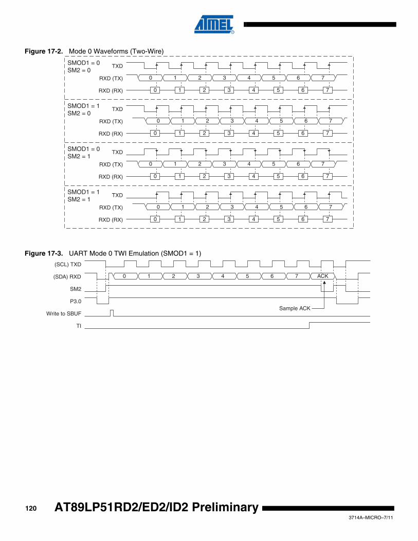
Figure 17-2. Mode 0 Waveforms (Two-Wire)
Figure 17-3. UART Mode 0 TWI Emulation (SMOD1 = 1)
7RXD (TX)
TXD
6543210
RXD (RX) 0 1 2 3 4 5 6 7
7RXD (TX)
TXD
6543210
RXD (RX) 0 1 2 3 4 5 6 7
7RXD (TX)
TXD
6543210
RXD (RX) 0 1 2 3 4 5 6 7
7RXD (TX)
TXD
6543210
RXD (RX) 0 1 2 3 4 5 6 7
SMOD1 = 0SM2 = 0
SMOD1 = 1SM2 = 0
SMOD1 = 0SM2 = 1
SMOD1 = 1SM2 = 1
7 (SDA) RXD
(SCL) TXD
6543210 ACK
SM2
P3.0
Write to SBUF
TI
Sample ACK
1203714A–MICRO–7/11
AT89LP51RD2/ED2/ID2 Preliminary

AT89LP51RD2/ED2/ID2 Preliminary
Figure 17-4. Serial Port Mode 0 (Two-Wire)
INTERNAL B U S
f sys
INTERNAL B U S
TXD (SHIFT CLOCK)
RXD ( D A T A OUT )
TXD (SHIFT CLOCK)
RXD ( D A T A IN )
WRITE T O S B U F
SEND
SHIFT
TI
WRITE T O SCON (CLEAR RI )
SHIFT
RECEIVE
RI
“1“
÷2
TB8
0 1
TIMER 1 O VERF L O W
÷2
SMOD1
0 1
SM2
1213714A–MICRO–7/11
17.6 More About Mode 1Ten bits are transmitted (through TXD), or received (through RXD): a start bit (0), 8 data bits(LSB first), and a stop bit (1). On receive, the stop bit goes into RB8 in SCON. In theAT89LP51RD2/ED2/ID2, the baud rate is determined either by the Timer 1 overflow rate, theTImer 2 overflow rate, or both. In this case one timer is for transmit and the other is for receive.Figure 17-5 shows a simplified functional diagram of the serial port in Mode 1 and associatedtimings for transmit and receive.
Transmission is initiated by any instruction that uses SBUF as a destination register. The “writeto SBUF” signal also loads a “1” into the 9th bit position of the transmit shift register and flags theTX Control unit that a transmission is requested. Transmission actually commences at S1P1 ofthe machine cycle following the next rollover in the divide-by-16 counter. Thus, the bit times aresynchronized to the divide-by-16 counter, not to the “write to SBUF” signal.
The transmission begins when SEND is activated, which puts the start bit at TXD. One bit timelater, DATA is activated, which enables the output bit of the transmit shift register to TXD. Thefirst shift pulse occurs one bit time after that.
As data bits shift out to the right, “0”s are clocked in from the left. When the MSB of the data byteis at the output position of the shift register, the “1” that was initially loaded into the 9th position isjust to the left of the MSB, and all positions to the left of that contain “0”s. This condition flags theTX Control unit to do one last shift, then deactivate SEND and set TI. This occurs at the tenthdivide-by-16 rollover after “write to SBUF.”
Reception is initiated by a 1-to-0 transition detected at RXD. For this purpose, RXD is sampledat a rate of 16 times the established baud rate. When a transition is detected, the divide-by-16counter is immediately reset, and 1FFH is written into the input shift register. Resetting thedivide-by-16 counter aligns its roll-overs with the boundaries of the incoming bit times.
The 16 states of the counter divide each bit time into 16ths. At the 7th, 8th, and 9th counterstates of each bit time, the bit detector samples the value of RXD. The value accepted is thevalue that was seen in at least 2 of the 3 samples. This is done to reject noise. In order to rejectfalse bits, if the value accepted during the first bit time is not 0, the receive circuits are reset andthe unit continues looking for another 1-to-0 transition. If the start bit is valid, it is shifted into theinput shift register, and reception of the rest of the frame proceeds.
As data bits come in from the right, “1”s shift out to the left. When the start bit arrives at the left-most position in the shift register, (which is a 9-bit register in Mode 1), it flags the RX Controlblock to do one last shift, load SBUF and RB8, and set RI. The signal to load SBUF and RB8and to set RI is generated if, and only if, the following conditions are met at the time the final shiftpulse is generated.
RI = 0 and
Either SM2 = 0, or the received stop bit = 1
If either of these two conditions is not met, the received frame is irretrievably lost. If both condi-tions are met, the stop bit goes into RB8, the 8 data bits go into SBUF, and RI is activated. Atthis time, whether or not the above conditions are met, the unit continues looking for a 1-to-0transition in RXD.
1223714A–MICRO–7/11
AT89LP51RD2/ED2/ID2 Preliminary

AT89LP51RD2/ED2/ID2 Preliminary
Figure 17-5. Serial Port Mode 1
TXCLOCK
WRITE TO SBUF
INTERNAL BUS
READSBUF
LOADSBUF
SBUF
SHIFT
INPUT SHIFT REG.(9 BITS)
BITDETECTOR
1-TO-0TRANSITIONDETECTOR
SERIALPORT
INTERRUPT
WRITETO
SBUF÷2
SMOD1
“0” “1”
TIMER 1OVERFLOW
RXD
RX CLOCK
RX CLOCK
RX CONTROLSTART
START DATA
SEND
SAMPLE
÷16
÷16TX CONTROL
TITI
ZERO DETECTOR
SBUFTXD
INTERNAL BUS
“1”
D QCL
S
LOADSBUFSHIFT
SHIFT
1FFH
RI
SEND
DATA
SHIFT
TXD
TI
D0 D1 D2 D3 D4 D5 D6 D7
D0 D1 D2 D3 D4 D5 D6 D7
STOP BIT
TR
AN
SM
IT
START BIT
÷16 RESET
START BIT STOP BIT
RXCLOCK
BIT DETECTOR SAMPLE TIMES
SHIFT
RE
CE
IVE RXD
RI
TIMER 2OVERFLOW
TCLK
RCLK
“0”
“0”
“1”
“1”
1233714A–MICRO–7/11

17.7 More About Modes 2 and 3Eleven bits are transmitted (through TXD), or received (through RXD): a start bit (0), 8 data bits(LSB first), a programmable 9th data bit, and a stop bit (1). On transmit, the 9th data bit (TB8)can be assigned the value of “0” or “1”. On receive, the 9th data bit goes into RB8 in SCON. Thebaud rate is programmable to either 1/16 or 1/32 of the oscillator frequency in Mode 2. Mode 3may have a variable baud rate generated from either Timer 1 or Timer 2, depending on the stateof RCLK and TCLK.
Figures 17-6 and 17-7 show a functional diagram of the serial port in Modes 2 and 3. Thereceive portion is exactly the same as in Mode 1. The transmit portion differs from Mode 1 onlyin the 9th bit of the transmit shift register.
Transmission is initiated by any instruction that uses SBUF as a destination register. The “writeto SBUF” signal also loads TB8 into the 9th bit position of the transmit shift register and flags theTX Control unit that a transmission is requested. Transmission commences at S1P1 of themachine cycle following the next rollover in the divide-by-16 counter. Thus, the bit times are syn-chronized to the divide-by-16 counter, not to the “write to SBUF” signal.
The transmission begins when SEND is activated, which puts the start bit at TXD. One bit timelater, DATA is activated, which enables the output bit of the transmit shift register to TXD. Thefirst shift pulse occurs one bit time after that. The first shift clocks a “1” (the stop bit) into the 9thbit position of the shift register. Thereafter, only “0”s are clocked in. Thus, as data bits shift out tothe right, “0”s are clocked in from the left. When TB8 is at the output position of the shift register,then the stop bit is just to the left of TB8, and all positions to the left of that contain “0”s. This con-dition flags the TX Control unit to do one last shift, then deactivate SEND and set TI. This occursat the 11th divide-by-16 rollover after “write to SBUF.”
Reception is initiated by a 1-to-0 transition detected at RXD. For this purpose, RXD is sampledat a rate of 16 times the established baud rate. When a transition is detected, the divide-by-16counter is immediately reset, and 1FFH is written to the input shift register.
At the 7th, 8th and 9th counter states of each bit time, the bit detector samples the value of RXD.The value accepted is the value that was seen in at least 2 of the 3 samples. If the valueaccepted during the first bit time is not 0, the receive circuits are reset and the unit continueslooking for another 1-to-0 transition. If the start bit proves valid, it is shifted into the input shiftregister, and reception of the rest of the frame proceeds.
As data bits come in from the right, “1”s shift out to the left. When the start bit arrives at the left-most position in the shift register (which in Modes 2 and 3 is a 9-bit register), it flags the RX Con-trol block to do one last shift, load SBUF and RB8, and set RI. The signal to load SBUF and RB8and to set RI is generated if, and only if, the following conditions are met at the time the final shiftpulse is generated:
RI = 0, and
Either SM2 = 0 or the received 9th data bit = 1
If either of these conditions is not met, the received frame is irretrievably lost, and RI is not set. Ifboth conditions are met, the received 9th data bit goes into RB8, and the first 8 data bits go intoSBUF. One bit time later, whether the above conditions were met or not, the unit continues look-ing for a 1-to-0 transition at the RXD input.
Note that the value of the received stop bit is irrelevant to SBUF, RB8, or RI.
1243714A–MICRO–7/11
AT89LP51RD2/ED2/ID2 Preliminary

AT89LP51RD2/ED2/ID2 Preliminary
Figure 17-6. Serial Port Mode 2
SMOD1 1
SMOD1 0
INTERNAL BUS
INTERNAL BUS
CPU CLOCK
1253714A–MICRO–7/11

Figure 17-7. Serial Port Mode 3
TXCLOCK
WRITE TO SBUF
SEND
DATA
SHIFT
TXD
STOP BIT GEN
TI
D0 D1 D2 D3 D4 D5 D6 D7 TB8 STOP BIT
TR
AN
SM
IT
START BIT
INTERNAL BUS
READSBUF
LOADSBUF
SBUF
SHIFT
INPUT SHIFT REG.(9 BITS)
BITDETECTOR
1-TO-0TRANSITIONDETECTOR
SERIALPORT
INTERRUPT
WRITETO
SBUF÷2
SMOD1
TIMER 1OVERFLOW
RXD
RX CLOCK
RX CLOCK
RX CONTROLSTART
START DATA
SAMPLE
÷16
÷16
TX CONTROL
TI
ZERO DETECTOR
SBUFTXD
INTERNAL BUS
TB8
D QCL
S
LOADSBUFSHIFT1FFH
SHIFT
RI
SEND
D0 D1 D2 D3 D4 D5 D6 D7 RB8START BIT STOPBIT
÷16 RESETRXCLOCK
BIT DETECTOR SAMPLE TIMES
SHIFT
RE
CE
IVE
RXD
RI
STOP BIT
TIMER 2OVERFLOW
TCLK
RCLK
“0”
“0”
“1”
“1”
“0” “1”
1263714A–MICRO–7/11
AT89LP51RD2/ED2/ID2 Preliminary

AT89LP51RD2/ED2/ID2 Preliminary
18. Enhanced Serial Peripheral InterfaceThe Serial Peripheral Interface (SPI) allows high-speed, full-duplex synchronous data transferbetween the AT89LP51RD2/ED2/ID2 and peripheral devices or between multiple microcon-troller devices, including multiple masters and slaves on a single bus. The SPI includes thefollowing features:
• Full-duplex, 3-wire or 4-wire Synchronous Data Transfer
• Master or Slave Operation
• Maximum Bit Frequency = fSYS/2
• LSB First or MSB First Data Transfer
• Seven Programmable Bit Rates or Timer 1-based Baud Generation (Master Mode)
• End of Transmission Interrupt Flag
• Write Collision Flag Protection
• Double-buffered Receive and Transmit
• Transmit Buffer Empty Interrupt Flag
• Mode Fault (Master Collision) Detection and Interrupt
• Wake up from Idle Mode
A block diagram of the SPI is shown below in Figure 18-1.
Figure 18-1. SPI Block Diagram
FPERIPH8-bit Shift Register
Read Data Buf f e r
Pin
Con
trol
Log
ic
SPI Control
SPI Status Register
SPI Inter r up t Request
Inte r na l Data Bus
Clock SelectSPI Clock (Master)
7-bit Divider
SPI Control Register
8
8
8
SP
IF
WC
OL
SP
R1
MSTR
SP
R2
Clo c k Logic
MSB
S
M
SP
EN
SS
DIS
MS
TR
CP
OL
CP
HA
SP
R1
SP
R0
MS
TR
SP
EN
DO
RD
LSB
S
M M
S
MISO
MOSI
SCK
SS
SP
R0
SPEN
W r ite Data Buf f e r
SS
ER
R
MO
DF
TB
IE
T1 OVF
RE
MA
P
DO
RD
SP
R2
TX
E
1273714A–MICRO–7/11
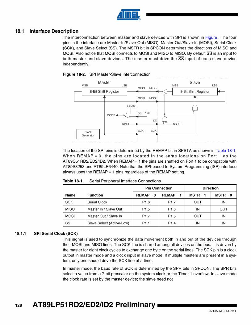
18.1 Interface DescriptionThe interconnection between master and slave devices with SPI is shown in Figure . The fourpins in the interface are Master-In/Slave-Out (MISO), Master-Out/Slave-In (MOSI), Serial Clock(SCK), and Slave Select (SS). The MSTR bit in SPCON determines the directions of MISO andMOSI. Also notice that MOSI connects to MOSI and MISO to MISO. By default SS is an input toboth master and slave devices. The master must drive the SS input of each slave deviceindependently.
Figure 18-2. SPI Master-Slave Interconnection
The location of the SPI pins is determined by the REMAP bit in SPSTA as shown in Table 18-1.When REMAP = 0, the p ins a re loca ted in the same loca t ions on Port 1 as theAT89C51RD2/ED2/ID2. When REMAP = 1 the pins are shuffled on Port 1 to be compatible withAT89S8253 and AT89LP6440. Note that the SPI-based In-System Programming (ISP) interfacealways uses the REMAP = 1 pins regardless of the REMAP setting.
18.1.1 SPI Serial Clock (SCK)This signal is used to synchronize the data movement both in and out of the devices throughtheir MOSI and MISO lines. The SCK line is shared among all devices on the bus. It is driven bythe master for eight clock cycles to exchange one byte on the serial lines. The SCK pin is a clockoutput in master mode and a clock input in slave mode. If multiple masters are present in a sys-tem, only one should drive the SCK line at a time.
In master mode, the baud rate of SCK is determined by the SPR bits in SPCON. The SPR bitsselect a value from a 7-bit prescaler on the system clock or the Timer 1 overflow. In slave modethe clock rate is set by the master device; the slave need not
Table 18-1. Serial Peripheral Interface Connections
Name Function
Pin Connection Direction
REMAP = 0 REMAP = 1 MSTR = 1 MSTR = 0
SCK Serial Clock P1.6 P1.7 OUT IN
MISO Master In / Slave Out P1.5 P1.6 IN OUT
MOSI Master Out / Slave In P1.7 P1.5 OUT IN
SS Slave Select (Active-Low) P1.1 P1.4 IN IN
8-Bit Shift Register
Master Slave MSB LSB MSB LSB
8-Bit Shift Register MISO MISO
SSDIS
MOSI MOSI
SS
SS
GPIO
SSDIS
VCC
SCK SCK
MODF
Clock Generator
1283714A–MICRO–7/11
AT89LP51RD2/ED2/ID2 Preliminary

AT89LP51RD2/ED2/ID2 Preliminary
18.1.2 Master Output / Slave Input (MOSI)This 1-bit signal is directly connected between the master device and all slave devices. TheMOSI line is used to transfer data in series from the master to the slave. Therefore, it is an out-put signal from the master, and an input signal to a slave. A byte (8-bit word) is normallytransmitted most significant bit (MSB) first, least significant bit (LSB) last. The DORD bit inSPSTA can change the data ordering to LSB first and MSB last. All devices on the same busshould share the same data order. If multiple masters are present in a system, only one shoulddrive the MOSI line at a time.
18.1.3 Master Input / Slave Output (MISO)This 1-bit signal is directly connected between all slave devices and a master device. The MISOline is used to transfer data in series from a slave to the master. Therefore, it is an output signalfrom the slave, and an input signal to the master. A byte (8-bit word) is transmitted most signifi-cant bit (MSB) first, least significant bit (LSB) last. The DORD bit in SPSTA can change the dataordering to LSB first anf MSB last. All devices on the same bus should share the same dataorder. When multiple slaves are present in a system, only the slave with its SS input low willdrive MISO.
18.1.4 Slave Select (SS)Each slave peripheral is selected by one Slave Select pin (SS). This signal must stay low for anymessage for a slave. It is obvious that only one master can drive the network at a time. The mas-ter may select each slave device by software through port pins. To prevent bus conflicts on theMISO line, only one slave should be selected at a time by the master for a transmission.
In a master configuration, the SS line can be used in conjunction with the MODF flag in the SPIStatus register (SPSTA) to prevent multiple masters from driving MOSI and SCK (see Errorconditions).
A high level on the SS pin puts the MISO line of a Slave SPI in a high-impedance state.
The SS pin can be used as a general-purpose I/O if the following conditions are met:
• The device is configured as a Master and the SSDIS control bit in SPCON is set. This kind of configuration can be found when only one Master is driving the network and there is no way that the SS pin could be pulled low. Therefore, the MODF flag in the SPSTA will never be set(1).
• The Device is configured as a Slave with CPHA and SSDIS control bits set(2). This kind of configuration can happen when the system comprises one Master and one Slave only. Therefore, the device should always be selected and there is no reason that the Master uses the SS pin to select the communicating Slave device.
Note: 1. Clearing SSDIS control bit does not clear MODF.
2. Special care should be taken when setting SSDIS control bit when CPHA = ’0’ because in this mode the SS is used to start the transmission on some devices. This requirement does not apply to the AT89LP51RD2/ED2/ID2 itself.
The In-System Programming (ISP) interface also uses the SPI pins. Although the ISP protocol isSPI-based, the SS pin has special meaning and must be driven by the master as a frame delim-iter. SS cannot be tied to ground for ISP to function correctly.
When the SPI is configured as a Master (MSTR in SPCON is set), the operation of the SS pindepends on the setting of the Slave Select Disable bit, SSDIS. If SSDIS = 1, the SS pin is a gen-eral purpose output pin which does not affect the SPI system. Typically, the pin will be drivingthe SS pin of an SPI Slave. If SSDIS = 0, SS must be held high to ensure Master SPI operation.
1293714A–MICRO–7/11

If the SS pin is driven low by peripheral circuitry when the SPI is configured as a Master withSSIG = 0, the SPI system interprets this as another master selecting the SPI as a slave andstarting to send data to it. To avoid bus contention, the SPI system takes the following actions:
1. The MSTR bit in SPCON is cleared and the SPI system becomes a Slave. As a result of the SPI becoming a Slave, the MOSI and SCK pins become inputs.
2. The MODF Flag in SPSTA is set, and if the SPI interrupt is enabled, the interrupt rou-tine will be executed.
Thus, when interrupt-driven SPI transmission is used in Master mode, and there exists a possi-bility that SS may be driven low, the interrupt should always check that the MSTR bit is still set. Ifthe MSTR bit has been cleared by a slave select, it must be set by the user to re-enable SPIMaster mode.
18.1.5 Pin ConfigurationWhen the SPI is enabled (SPEN = 1), the data direction of the MOSI, MISO and SCK pins isautomatically overridden according to the MSTR bit as shown in Table 18-2. The user need notreconfigure the pins when switching from master to slave or vice-versa. For more details on portconfiguration, refer to “Port Configuration” on page 71..
Notes: 1. In these modes MOSI is active only during transfers. MOSI will be pulled high between trans-fers to allow other masters to control the line.
2. In Push-Pull mode MOSI is active only during transfers, otherwise it is tristated to prevent line contention. A weak external pull-up may be required to prevent MOSI from floating.
Table 18-2. SPI Pin Configuration and Behavior when SPE = 1
Pin Mode Master (MSTR = 1) Slave (MSTR = 0)
SCK
Quasi-bidirectional Output Input (Internal Pull-up)
Push-Pull Output Output Input (Tristate)
Input-Only No output (Tristated) Input (Tristate)
Open-Drain Output Output Input (External Pull-up)
MOSI
Quasi-bidirectional Output(1) Input (Internal Pull-up)
Push-Pull Output Output(2) Input (Tristate)
Input-Only No output (Tristated) Input (Tristate)
Open-Drain Output Output(1) Input (External Pull-up)
MISO
Quasi-bidirectional Input (Internal Pull-up)Output (SS = 0)
Internal Pull-up (SS = 1)
Push-Pull Output Input (Tristate)Output (SS = 0)
Tristated (SS = 1)
Input-Only Input (Tristate) No output (Tristated)
Open-Drain Output Input (External Pull-up)Output (SS = 0)
External Pull-up (SS = 1)
1303714A–MICRO–7/11
AT89LP51RD2/ED2/ID2 Preliminary

AT89LP51RD2/ED2/ID2 Preliminary
18.2 Master OperationAn SPI master device initiates all data transfers on the SPI bus. The AT89LP51RD2/ED2/ID2 isconfigured for master operation by setting MSTR = 1 in SPCON. Writing to the SPI data register(SPDAT) while in master mode loads the transmit buffer. If the SPI shift register is empty, thebyte in the transmit buffer is moved to the shift register; the transmit buffer empty flag, TXE, isset; and a transmission begins. The transfer may start after an initial delay, while the clock gen-erator waits for the next full bit slot of the specified baud rate. The master shifts the data outserially on the MOSI line while providing the serial shift clock on SCK. When the transfer fin-ishes, the SPIF flag is set to “1” and an interrupt request is generated, if enabled. The datareceived from the addressed SPI slave device is also transferred from the shift register to thereceive buffer. Therefore, the SPIF bit flags both the transmit-complete and receive-data-readyconditions. The received data is accessed by reading SPDAT.
While the TXE flag is set, the transmit buffer is empty. TXE can be cleared by software or bywriting to SPDAT. Writing to SPDAT will clear TXE and load the transmit buffer. The user mayload the buffer while the shift register is busy, i.e. before the current transfer completes. Whenthe current transfer completes, the queued byte in the transmit buffer is moved to the shift regis-ter and the next transfer commences. TXE will generate an interrupt if the SPI interrupt isenabled and if the ENH bit in SPSTA is set. For multi-byte transfers, TXE may be used toremove any dead time between byte transmissions.
The SPI master can operate in two modes: multi-master mode and single-master mode. Bydefault, multi-master mode is active when SSIG = 0. In this mode, the SS input is used to dis-able a master device when another master is accessing the bus. When SS is driven low, themaster device becomes a slave by clearing its MSTR bit and a Mode Fault is generated by set-ting the MODF bit in SPSTA. MODF will generate an interrupt if enabled. The MSTR bit must beset in software before the device may become a master again. Single-master mode is enabledby setting SSIG = 1. In this mode SS is ignored and the master is always active. SS may beused as a general purpose I/O in this mode.
18.3 Slave OperationWhen the AT89LP51RD2/ED2/ID2 is not configured for master operation, MSTR = 0, it will oper-ate as an SPI slave. In slave mode, bytes are shifted in through MOSI and out through MISO bya master device controlling the serial clock on SCK. When a byte has been transferred, the SPIFflag is set to “1” and an interrupt request is generated, if enabled. The data received from theaddressed master device is also transferred from the shift register to the receive buffer. Thereceived data is accessed by reading SPDAT. A slave device cannot initiate transfers. Data tobe transferred to the master device must be preloaded by writing to SPDAT. Writes to SPDATare double-buffered. The transmit buffer is loaded first and if the shift register is empty, the con-tents of the buffer will be transferred to the shift register.
While the TXE flag is set, the transmit buffer is empty. TXE can be cleared by software or bywriting to SPDAT. Writing to SPDAT will clear TXE and load the transmit buffer. The user mayload the buffer while the shift register is busy, i.e. before the current transfer completes. Whenthe current transfer completes, the queued byte in the transmit buffer is moved to the shift regis-ter and waits for the master to initiate another transfer. TXE will generate an interrupt if the SPIinterrupt is enabled and if the ENH bit in SPSTA is set.
The SPI slave can operate in two modes: 4-wire mode and 3-wire mode. By default, 4-wiremode is active when SSIG = 0. In this mode, the SS input is used to enable/disable the slavedevice when addressed by a master. When SS is driven low, the slave device is enabled and will
1313714A–MICRO–7/11

shift out data on MISO in response to the serial clock on SCK. While SS is high, the SPI slavewill remain sleeping with MISO inactive. Three-wire mode is enabled by setting SSIG = 1. In thismode SS is ignored and the slave is always active. SS may be used as a general purpose I/O inthis mode.
The Disable Slave Output bit, DISSO in SPSTA, may be used to disable the MISO line of a slavedevice. DISSO can allow several slave devices to share MISO while operating in 3-wire mode. Inthis case some protocol other than SS may be used to determine which slave is enabled.
18.4 Error ConditionsThe following flags in the SPSTA signal SPI error conditions:
18.4.1 Mode Fault (MODF)Mode Fault error in Master mode SPI indicates that the level on the Slave Select (SS) pin isinconsistent with the actual mode of the device. MODF is set to warn that there may be a multi-master conflict for system control. In this case, the SPI system is affected in the following ways:
• An SPI receiver/error CPU interrupt request is generated
• The SPEN bit in SPCON is cleared. This disables the SPI
• The MSTR bit in SPCON is cleared
When SS Disable (SSDIS) bit in the SPCON register is cleared, the MODF flag is set when theSS signal becomes ’0’.
However, as stated before, for a system with one Master, if the SS pin of the Master device ispulled low, there is no way that another Master attempts to drive the network. In this case, toprevent the MODF flag from being set, software can set the SSDIS bit in the SPCON registerand therefore making the SS pin as a general-purpose I/O pin.
Clearing the MODF bit is accomplished by a read of SPSTA register with MODF bit set, followedby a write to the SPCON register. SPEN Control bit may be restored to its original set state afterthe MODF bit has been cleared.
18.4.2 Write Collision (WCOL)A Write Collision (WCOL) flag in the SPSTA is set when a write to the SPDAT register is doneduring a transmit sequence.
WCOL does not cause an interruption, and the transfer continues uninterrupted.
Clearing the WCOL bit is done through a software sequence of an access to SPSTA and anaccess to SPDAT.
18.4.3 Overrun ConditionAn overrun condition occurs when the Master device tries to send several data Bytes and theSlave devise has not cleared the SPIF bit issuing from the previous data Byte transmitted. In thiscase, the receiver buffer contains the Byte sent after the SPIF bit was last cleared. A read of theSPDAT returns this Byte. All others Bytes are lost.
This condition is not detected by the SPI peripheral.
1323714A–MICRO–7/11
AT89LP51RD2/ED2/ID2 Preliminary
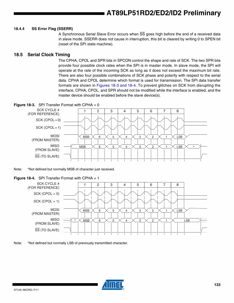
AT89LP51RD2/ED2/ID2 Preliminary
18.4.4 SS Error Flag (SSERR)A Synchronous Serial Slave Error occurs when SS goes high before the end of a received datain slave mode. SSERR does not cause in interruption, this bit is cleared by writing 0 to SPEN bit(reset of the SPI state machine).
18.5 Serial Clock TimingThe CPHA, CPOL and SPR bits in SPCON control the shape and rate of SCK. The two SPR bitsprovide four possible clock rates when the SPI is in master mode. In slave mode, the SPI willoperate at the rate of the incoming SCK as long as it does not exceed the maximum bit rate.There are also four possible combinations of SCK phase and polarity with respect to the serialdata. CPHA and CPOL determine which format is used for transmission. The SPI data transferformats are shown in Figures 18-3 and 18-4. To prevent glitches on SCK from disrupting theinterface, CPHA, CPOL, and SPR should not be modified while the interface is enabled, and themaster device should be enabled before the slave device(s).
Figure 18-3. SPI Transfer Format with CPHA = 0
Note: *Not defined but normally MSB of character just received.
Figure 18-4. SPI Transfer Format with CPHA = 1
Note: *Not defined but normally LSB of previously transmitted character.
MSB 6 5 4 3 2 1 LSB
1 2 3 4 5 6 7 8
MSB* 6 5 4 3 2 1 LSB
SCK CYCLE #(FOR REFERENCE)
SCK (CPOL = 0)
SCK (CPOL = 1)
MOSI(FROM MASTER)
MISO(FROM SLAVE)
SS (TO SLAVE)
1333714A–MICRO–7/11
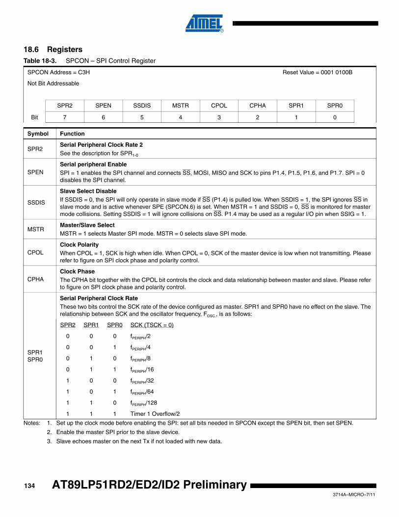
18.6 Registers
Notes: 1. Set up the clock mode before enabling the SPI: set all bits needed in SPCON except the SPEN bit, then set SPEN.
2. Enable the master SPI prior to the slave device.
3. Slave echoes master on the next Tx if not loaded with new data.
Table 18-3. SPCON – SPI Control Register
SPCON Address = C3H Reset Value = 0001 0100B
Not Bit Addressable
SPR2 SPEN SSDIS MSTR CPOL CPHA SPR1 SPR0
Bit 7 6 5 4 3 2 1 0
Symbol Function
SPR2Serial Peripheral Clock Rate 2See the description for SPR1-0
SPENSerial peripheral EnableSPI = 1 enables the SPI channel and connects SS, MOSI, MISO and SCK to pins P1.4, P1.5, P1.6, and P1.7. SPI = 0 disables the SPI channel.
SSDIS
Slave Select DisableIf SSDIS = 0, the SPI will only operate in slave mode if SS (P1.4) is pulled low. When SSDIS = 1, the SPI ignores SS in slave mode and is active whenever SPE (SPCON.6) is set. When MSTR = 1 and SSDIS = 0, SS is monitored for master mode collisions. Setting SSDIS = 1 will ignore collisions on SS. P1.4 may be used as a regular I/O pin when SSIG = 1.
MSTRMaster/Slave SelectMSTR = 1 selects Master SPI mode. MSTR = 0 selects slave SPI mode.
CPOLClock PolarityWhen CPOL = 1, SCK is high when idle. When CPOL = 0, SCK of the master device is low when not transmitting. Please refer to figure on SPI clock phase and polarity control.
CPHAClock PhaseThe CPHA bit together with the CPOL bit controls the clock and data relationship between master and slave. Please refer to figure on SPI clock phase and polarity control.
SPR1SPR0
Serial Peripheral Clock Rate These two bits control the SCK rate of the device configured as master. SPR1 and SPR0 have no effect on the slave. The relationship between SCK and the oscillator frequency, FOSC., is as follows:
SPR2 SPR1 SPR0 SCK (TSCK = 0)
0 0 0 fPERIPH/2
0 0 1 fPERIPH/4
0 1 0 fPERIPH/8
0 1 1 fPERIPH/16
1 0 0 fPERIPH/32
1 0 1 fPERIPH/64
1 1 0 fPERIPH/128
1 1 1 Timer 1 Overflow/2
1343714A–MICRO–7/11
AT89LP51RD2/ED2/ID2 Preliminary

AT89LP51RD2/ED2/ID2 Preliminary
Table 18-4. SPDAT – SPI Data Register
SPDAT Address = C5H Reset Value = 0000 0000
Not Bit Addressable
SPD7 SPD6 SPD5 SPD4 SPD3 SPD2 SPD1 SPD0
Bit 7 6 5 4 3 2 1 0
Table 18-5. SPSTA – SPI Status Register
SPSTA Address = C4H Reset Value = 0000 0000B
Not Bit Addressable
SPIF WCOL SSERR MODF TXE DORD REMAP TBIE
Bit 7 6 5 4 3 2 1 0
Symbol Function
SPIFSPI Transfer Complete Interrupt FlagWhen a serial transfer is complete, the SPIF bit is set by hardware and an interrupt is generated if ESP = 1. The SPIF bit may be cleared by software or by reading the SPI status register followed by reading/writing the SPI data register.
WCOLWrite Collision FlagThe WCOL bit is set by hardware if SPDAT is written while the transmit buffer is full. The ongoing transfer is not affected. WCOL may be cleared by software or by reading the SPI status register followed by reading/writing the SPI data register.
SSERRSS Slave Error FlagSet by hardware when SS is deasserted before the end of a received data byte.
MODFMode Fault FlagMODF is set by hardware when a master mode collision is detected (MSTR = 1, SSIG = 0 and SS = 0) and an interrupt is generated if ESP = 1. MODF must be cleared by software.
TXETransmit Buffer Empty FlagSet by hardware when the transmit buffer is loaded into the shift register, allowing a new byte to be loaded. TXE must be cleared by software. When ENH = 1 and ESP = 1, TXE will generate an interrupt.
DORDData orderDORD = 1 selects LSB first data transmission. DORD = 0 selects MSB first data transmission.
REMAPRemap SPI PinsWhen cleared the SPI pins are in the default locations on Port 1 that are compatible with AT89C51RD2/ED2/ID2. When set the pins are shuffled on Port 1 to match the AT89S8253 or AT89LP6440 devices. See Table 18-1.
TBIETX Buffer Interrupt EnableWhen TBIE = 1, TXE will generate an SPI interrupt if ESP = 1. When TBIE = 0, TXE does not generate an interrupt.
1353714A–MICRO–7/11

19. Two-Wire Serial InterfaceThe Two-Wire Interface (TWI) is a bi-directional 2-wire serial communication standard. It isdesigned primarily for simple but efficient integrated circuit (IC) control. The system is comprisedof two lines, SCL (Serial Clock) and SDA (Serial Data) that carry information between the ICsconnected to them. The only external hardware needed to implement the bus is a single pull-upresistor for each of the TWI bus lines. All devices connected to the bus have individualaddresses, and mechanisms for resolving bus contention are inherent in the TWI protocol. Theserial data transfer is limited to 400Kbit/s in standard mode. Various communication configura-tions can be designed using this bus. Figure 19-1 shows a typical 2-wire bus configuration. Anyof the devices connected to the bus can be master or slave.
The Two-Wire Interface on the AT89LP51RD2/ED2/ID2 provides the following features:
• Simple Yet Powerful and Flexible Communication Interface, only two Bus Lines Needed
• Both Master and Slave Operation Supported
• Device can Operate as Transmitter or Receiver
• 7-bit Address Space Allows up to 128 Different Slave Addresses
• Multi-master Arbitration Support
• Up to 400 kHz Data Transfer Speed
• Fully Programmable Slave Address with General Call Support
Note: The TWI is available on both the AT89LP51RD2 and AT89LP51ED2 where as it was not available on the AT89C51RD2 and AT89C51ED2. The TWI is not available in the PDIP package.
Figure 19-1. Two-Wire Bus Configuration
As depicted in Figure 19-1, both bus lines are connected to the positive supply voltage throughpull-up resistors. The bus drivers of all TWI-compliant devices are open-drain or open-collector.This implements a wired-AND function which is essential to the operation of the interface. A lowlevel on a TWI bus line is generated when one or more TWI devices output a zero. A high levelis output when all TWI devices tristate their outputs, allowing the pull-up resistors to pull the linehigh. Note that all AT89LP devices connected to the TWI bus must be powered in order to allowany bus operation. The number of devices that can be connected to the bus is only limited by thebus capacitance limit of 400 pF and the 7-bit slave address space.
Device 1 Device 2 Device 3 Device n
SDA
SCL
........ R1 R2
VCC
1363714A–MICRO–7/11
AT89LP51RD2/ED2/ID2 Preliminary

AT89LP51RD2/ED2/ID2 Preliminary
19.1 Data Transfer and Frame Format
19.1.1 Transferring BitsEach data bit transferred on the TWI bus is accompanied by a pulse on the clock line. The levelof the data line must be stable when the clock line is high. The only exception to this rule is forgenerating start and stop conditions.
Figure 19-2. Data Validity
19.1.2 START and STOP ConditionsThe Master initiates and terminates a data transmission. The transmission is initiated when theMaster issues a START condition on the bus, and it is terminated when the Master issues aSTOP condition. Between a START and a STOP condition, the bus is considered busy, and noother Master should try to seize control of the bus. A special case occurs when a new STARTcondition is issued between a START and STOP condition. This is referred to as a REPEATEDSTART condition, and is used when the Master wishes to initiate a new transfer without relin-quishing control of the bus. After a REPEATED START, the bus is considered busy until the nextSTOP. This is identical to the START behavior, and therefore START is used to describe bothSTART and REPEATED START for the remainder of this data sheet, unless otherwise noted.As depicted below, START and STOP conditions are signalled by changing the level of the SDAline when the SCL line is high.
Figure 19-3. START, REPEATED START, and STOP Conditions
19.1.3 Address Packet FormatAll address packets transmitted on the TWI bus are nine bits long, consisting of seven addressbits, one READ/WRITE control bit and an acknowledge bit. If the READ/WRITE bit is set, a readoperation is to be performed, otherwise a write operation should be performed. When a slaverecognizes that it is being addressed, it should acknowledge by pulling SDA low in the ninth SCL(ACK) cycle. If the addressed Slave is busy, or for some other reason can not service the Mas-
SDA
SCL
Data Stable Data Stable
Data Change
SDA
SCL
START STOPREPEATED STARTSTOP START
1373714A–MICRO–7/11

ter’s request, the SDA line should be left high in the ACK clock cycle. The Master can thentransmit a STOP condition, or a REPEATED START condition to initiate a new transmission. Anaddress packet consisting of a slave address and a READ or a WRITE bit is called SLA+R orSLA+W, respectively.
The MSB of the address byte is transmitted first. Slave addresses can freely be allocated by thedesigner, but the address 0000 000 is reserved for a general call.
When a general call is issued, all slaves should respond by pulling the SDA line low in the ACKcycle. A general call is used when a Master wishes to transmit the same message to severalslaves in the system. When the general call address followed by a write bit is transmitted on thebus, all slaves set up to acknowledge the general call will pull the SDA line low in the ACK cycle.The following data packets will then be received by all the slaves that acknowledged the generalcall. Note that transmitting the general call address followed by a Read bit is meaningless, asthis would cause contention if several slaves started transmitting different data.
All addresses of the format 1111 xxx should be reserved for future purposes.
Figure 19-4. Address Packet Format
19.1.4 Data Packet FormatAll data packets transmitted on the TWI bus are nine bits long, consisting of one data byte andan acknowledge bit. During a data transfer, the Master generates the clock and the START andSTOP conditions, while the Receiver is responsible for acknowledging the reception. AnAcknowledge (ACK) is signalled by the Receiver pulling the SDA line low during the ninth SCLcycle. If the Receiver leaves the SDA line high, a NACK is signalled. When the Receiver hasreceived the last byte, or for some reason cannot receive any more bytes, it should inform theTransmitter by sending a NACK after the final byte. The MSB of the data byte is transmitted first.
Figure 19-5. Data Packet Format
SDA
SCL
START
1 2 7 8 9
Addr MSB Addr LSB R/W ACK
1 2 7 8 9
Data MSB Data LSB ACK
AggregateSDA
SDA fromTransmitter
SDA fromReceiver
SCL fromMaster
SLA+R/W Data ByteSTOP, REPEATED
START, or NextData Byte
1383714A–MICRO–7/11
AT89LP51RD2/ED2/ID2 Preliminary

AT89LP51RD2/ED2/ID2 Preliminary
19.1.5 Combining Address and Data Packets Into a TransmissionA transmission basically consists of a START condition, a SLA+R/W, one or more data packetsand a STOP condition. An empty message, consisting of a START followed by a STOP condi-tion, is illegal. Note that the wired-ANDing of the SCL line can be used to implementhandshaking between the Master and the Slave. The Slave can extend the SCL low period bypulling the SCL line low. This is useful if the clock speed set up by the Master is too fast for theSlave, or the Slave needs extra time for processing between the data transmissions. The Slaveextending the SCL low period will not affect the SCL high period, which is determined by theMaster. As a consequence, the Slave can reduce the TWI data transfer speed by prolonging theSCL duty cycle.
Figure 19-6 shows a typical data transmission. Note that several data bytes can be transmittedbetween the SLA+R/W and the STOP condition, depending on the software protocol imple-mented by the application software.
Figure 19-6. Typical Data Transmission
19.2 Multi-master Bus Systems, Arbitration and SynchronizationThe TWI protocol allows bus systems with several masters. Special concerns have been takenin order to ensure that transmissions will proceed as normal, even if two or more masters initiatea transmission at the same time. Two problems arise in multi-master systems:
• An algorithm must be implemented allowing only one of the masters to complete the transmission. All other masters should cease transmission when they discover that they have lost the selection process. This selection process is called arbitration. When a contending master discovers that it has lost the arbitration process, it should immediately switch to Slave mode to check whether it is being addressed by the winning master. The fact that multiple masters have started transmission at the same time should not be detectable to the slaves (i.e., the data being transferred on the bus must not be corrupted).
• Different masters may use different SCL frequencies. A scheme must be devised to synchronize the serial clocks from all masters, in order to let the transmission proceed in a lockstep fashion. This will facilitate the arbitration process.
The wired-ANDing of the bus lines is used to solve both these problems. The serial clocks fromall masters will be wired-ANDed, yielding a combined clock with a high period equal to the onefrom the master with the shortest high period. The low period of the combined clock is equal tothe low period of the master with the longest low period. Note that all masters listen to the SCLline, effectively starting to count their SCL high and low Time-out periods when the combinedSCL line goes high or low, respectively.
1 2 7 8 9
Data Byte
Data MSB Data LSB ACK
SDA
SCL
START
1 2 7 8 9
Addr MSB Addr LSB R/W ACK
SLA+R/W STOP
1393714A–MICRO–7/11

Figure 19-7. SCL Synchronization between Multiple Masters
Arbitration is carried out by all masters continuously monitoring the SDA line after outputtingdata. If the value read from the SDA line does not match the value the master had output, it haslost the arbitration. Note that a master can only lose arbitration when it outputs a high SDA valuewhile another master outputs a low value. The losing master should immediately go to Slavemode, checking if it is being addressed by the winning master. The SDA line should be left high,but losing masters are allowed to generate a clock signal until the end of the current data oraddress packet. Arbitration will continue until only one master remains, and this may take manybits. If several masters are trying to address the same slave, arbitration will continue into thedata packet.
Figure 19-8. Arbitration between Two Masters
Note that arbitration is not allowed between:
• A REPEATED START condition and a data bit.
• A STOP condition and a data bit.
• A REPEATED START and a STOP condition.
TA low TA high
SCL fromMaster A
SCL fromMaster B
SCL busLine
TBlow TBhigh
Masters StartCounting Low Period
Masters StartCounting High Period
SDA fromMaster A
SDA fromM
SDA Line
SynchronizedSCL Line
STARTMaster A Loses
Arbitration, SDAA SDA
1403714A–MICRO–7/11
AT89LP51RD2/ED2/ID2 Preliminary

AT89LP51RD2/ED2/ID2 Preliminary
It is the user software’s responsibility to ensure that these illegal arbitration conditions neveroccur. This implies that in multi-master systems, all data transfers must use the same composi-tion of SLA+R/W and data packets. In other words: All transmissions must contain the samenumber of data packets, otherwise the result of the arbitration is undefined.
19.3 Overview of the TWI ModuleThe TWI module is comprised of several submodules, as shown in Figure 19-9. All registersdrawn in a thick line are accessible through the AT89LP data bus.
Figure 19-9. Overview of the TWI Module
19.3.1 SCL and SDA PinsThese pins interface the TWI with the rest of the MCU system. The output drivers contain a slew-rate limiter in order to conform to the TWI specification. The input stages contain a spike sup-pression unit removing spikes shorter than 50 ns.
19.3.2 Bit Rate Generator UnitThis unit controls the period of SCL when operating in a Master mode. The SCL period is con-trolled by settings in the SSCON register. Slave operation does not depend on the Bit Ratesetting, but the CPU clock frequency in the slave must be at least 16 times higher than the SCLfrequency. Note that slaves may prolong the SCL low period, thereby reducing the average TWIbus clock period. The SCL frequency is generated according to Table 19-1.
TW
I Uni
t
Address Register (SSADR)
Address Match Unit
Address Comparator
Control Unit
Control Register (SSCON)
Status Register (SSCS)
State Machine and Status Control
SCL
Slew-rate Control
Spike Filter
SDA
Slew-rate Control
Spike Filter
Bit Rate Generator
Timer 1 Overflow
Prescaler
Bus Interface Unit
START / STOP Control
Arbitration Detection Ack
Spike Suppression
Address/Data Shift Register (SSDAT)
1413714A–MICRO–7/11
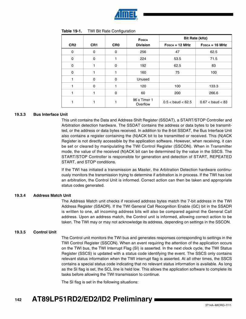
19.3.3 Bus Interface UnitThis unit contains the Data and Address Shift Register (SSDAT), a START/STOP Controller andArbitration detection hardware. The SSDAT contains the address or data bytes to be transmit-ted, or the address or data bytes received. In addition to the 8-bit SSDAT, the Bus Interface Unitalso contains a register containing the (N)ACK bit to be transmitted or received. This (N)ACKRegister is not directly accessible by the application software. However, when receiving, it canbe set or cleared by manipulating the TWI Control Register (SSCON). When in Transmittermode, the value of the received (N)ACK bit can be determined by the value in the SSCS. TheSTART/STOP Controller is responsible for generation and detection of START, REPEATEDSTART, and STOP conditions.
If the TWI has initiated a transmission as Master, the Arbitration Detection hardware continu-ously monitors the transmission trying to determine if arbitration is in process. If the TWI has lostan arbitration, the Control Unit is informed. Correct action can then be taken and appropriatestatus codes generated.
19.3.4 Address Match UnitThe Address Match unit checks if received address bytes match the 7-bit address in the TWIAddress Register (SSADR). If the TWI General Call Recognition Enable (GC) bit in the SSADRis written to one, all incoming address bits will also be compared against the General Calladdress. Upon an address match, the Control unit is informed, allowing correct action to betaken. The TWI may or may not acknowledge its address, depending on settings in the SSCON.
19.3.5 Control UnitThe Control unit monitors the TWI bus and generates responses corresponding to settings in theTWI Control Register (SSCON). When an event requiring the attention of the application occurson the TWI bus, the TWI Interrupt Flag (SI) is asserted. In the next clock cycle, the TWI StatusRegister (SSCS) is updated with a status code identifying the event. The SSCS only containsrelevant status information when the TWI interrupt flag is asserted. At all other times, the SSCScontains a special status code indicating that no relevant status information is available. As longas the SI flag is set, the SCL line is held low. This allows the application software to complete itstasks before allowing the TWI transmission to continue.
The SI flag is set in the following situations:
Table 19-1. TWI Bit Rate Configuration
CR2 CR1 CR0FOSCA
Division
Bit Rate (kHz)
FOSCA = 12 MHz FOSCA = 16 MHz
0 0 0 256 47 62.5
0 0 1 224 53.5 71.5
0 1 0 192 62.5 83
0 1 1 160 75 100
1 0 0 Unused
1 0 1 120 100 133.3
1 1 0 60 200 266.6
1 1 196 x Timer 1
Overflow0.5 < baud < 62.5 0.67 < baud < 83
1423714A–MICRO–7/11
AT89LP51RD2/ED2/ID2 Preliminary

AT89LP51RD2/ED2/ID2 Preliminary
• After the TWI has transmitted a START/REPEATED START condition.
• After the TWI has transmitted SLA+R/W.
• After the TWI has transmitted an address byte.
• After the TWI has lost arbitration.
• After the TWI has been addressed by own slave address or general call.
• After the TWI has received a data byte.
• After a STOP or REPEATED START has been received while still addressed as a Slave.
• When a bus error has occurred due to an illegal START or STOP condition.
19.4 Register Overview
Table 19-2. SSCON – Two-Wire Control Register
SSCON Address = AAH Reset Value = X000 00XXB
Not Bit Addressable
CR2 SSIE STA STO SI AA CR1 CR0
Bit 7 6 5 4 3 2 1 0
Symbol Function
CR2Bit Control Rate 2Sets the bit rate for TWI master mode along with C1 and CR0. See Table 19-1.
SSIETwo-wire Serial Interface EnableSet to enable the TWI. Clear to disable the TWI.
STAStart FlagSet to send a START condition on the bus. Must be cleared by software.
STOStop FlagSet to send a STOP condition on the bus. Cleared automatically by hardware when the STOP occurs.
SI
Two-wire Interface Interrupt FlagSet by hardware when the TWI requests an interrupt. SI must be cleared by software. While SI is set, the SCL low period is stretched. Note that clearing this flag starts the operation of the TWI, so all accesses to the other TWI registers (SSADR, SSCS and SSDAT) must be complete before clearing this flag.
AA
Assert Acknowledge FlagClear in master and slave receiver modes, to force a not acknowledge (high level on SDA). Clear to disable SLA or GCA recognition. Set to recognize SLA or GCA (if GC set) for entering slave receiver or transmitter modes. Set in master and slave receiver modes, to force an acknowledge (low level on SDA). This bit has no effect when in master transmitter mode. By clearing AA to zero, the device can be virtually disconnected from the Two-wire Serial Bus temporarily. Address recognition can then be resumed by setting the AA bit to one again.
CR1Bit Control Rate 1Sets the bit rate for TWI master mode along with C0 and CR2. See Table 19-1.
CR0Bit Control Rate 02Sets the bit rate for TWI master mode along with C1 and CR2. See Table 19-1.
1433714A–MICRO–7/11

19.5 Using the TWIThe AT89LP TWI is byte-oriented and interrupt based. Interrupts are issued after all bus events,like reception of a byte or transmission of a START condition. Because the TWI is interrupt-based, the application software is free to carry on other operations during a TWI byte transfer.Note that the TWI Interrupt Enable (ETWI) bit in IE2 together with the Global Interrupt Enable bitin EA allow the application to decide whether or not assertion of the SI flag should generate an
Table 19-3. SSCS – Two-Wire Status Register
SSCS Address = ABH Reset Value = 1111 1000B
Not Bit Addressable
SC7 SC6 SC5 SC4 SC3 0 0 0
Bit 7 6 5 4 3 2 1 0
Symbol Function
SC7-0
Two-wire Interface StatusThe current status code of the TWI logic and serial bus. See Table 19-6 through Table 19-10 for a description of the status codes. Note that the three least significant bits always read as zero. The Status code is valid only while SI remains set.
Table 19-4. SSADR – Two-Wire Address Register
SSADR Address = ACH Reset Value = 1111 1110B
Not Bit Addressable
SA6 SA5 SA4 SA3 SA2 SA1 SA0 GC
Bit 7 6 5 4 3 2 1 0
Symbol Function
SA6-0Two-wire Interface Slave AddressThe TWI will only respond to slave addresses that match this 7-bit address.
GCGeneral Call EnableSet to enable General Call address (00h) recognition. Clear to disable General Call address recognition.
Table 19-5. SSDAT – Two-Wire Data Register
SSDAT Address = ADH Reset Value = 1111 1111B
Not Bit Addressable
SD7 SD6 SD5 SD4 SD3 SD2 SD1 SD0
Bit 7 6 5 4 3 2 1 0
Symbol Function
SD7-0
Two-wire Interface Serial DataWrites to SSDAT queue the next address or data byte for transmission. Reads from SSDAT return the last address or data byte present on the bus. Writes/reads to/from SSDAT must occur only while SI is set. Writes to SSDAT while SI = 0 are ignored. Reads from SSDAT while SI = 0 may return random data.
1443714A–MICRO–7/11
AT89LP51RD2/ED2/ID2 Preliminary
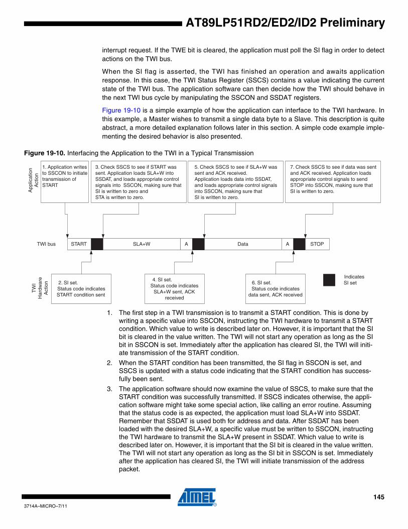
AT89LP51RD2/ED2/ID2 Preliminary
interrupt request. If the TWE bit is cleared, the application must poll the SI flag in order to detectactions on the TWI bus.
When the SI flag is asserted, the TWI has finished an operation and awaits applicationresponse. In this case, the TWI Status Register (SSCS) contains a value indicating the currentstate of the TWI bus. The application software can then decide how the TWI should behave inthe next TWI bus cycle by manipulating the SSCON and SSDAT registers.
Figure 19-10 is a simple example of how the application can interface to the TWI hardware. Inthis example, a Master wishes to transmit a single data byte to a Slave. This description is quiteabstract, a more detailed explanation follows later in this section. A simple code example imple-menting the desired behavior is also presented.
Figure 19-10. Interfacing the Application to the TWI in a Typical Transmission
1. The first step in a TWI transmission is to transmit a START condition. This is done by writing a specific value into SSCON, instructing the TWI hardware to transmit a START condition. Which value to write is described later on. However, it is important that the SI bit is cleared in the value written. The TWI will not start any operation as long as the SI bit in SSCON is set. Immediately after the application has cleared SI, the TWI will initi-ate transmission of the START condition.
2. When the START condition has been transmitted, the SI flag in SSCON is set, and SSCS is updated with a status code indicating that the START condition has success-fully been sent.
3. The application software should now examine the value of SSCS, to make sure that the START condition was successfully transmitted. If SSCS indicates otherwise, the appli-cation software might take some special action, like calling an error routine. Assuming that the status code is as expected, the application must load SLA+W into SSDAT. Remember that SSDAT is used both for address and data. After SSDAT has been loaded with the desired SLA+W, a specific value must be written to SSCON, instructing the TWI hardware to transmit the SLA+W present in SSDAT. Which value to write is described later on. However, it is important that the SI bit is cleared in the value written. The TWI will not start any operation as long as the SI bit in SSCON is set. Immediately after the application has cleared SI, the TWI will initiate transmission of the address packet.
START SLA+W A Data A STOP
1. Application writesto SSCON to initiatetransmission of START
2. SI set.Status code indicates START condition sent
4. SI set.Status code indicates
SLA+W sent, ACK received
6. SI set.Status code indicates
data sent, ACK received
3. Check SSCS to see if START was sent. Application loads SLA+W into SSDAT, and loads appropriate control signals into SSCON, making sure that SI is written to zero and STA is written to zero.
5. Check SSCS to see if SLA+W was sent and ACK received.Application loads data into SSDAT, and loads appropriate control signals into SSCON, making sure that SI is written to zero.
7. Check SSCS to see if data was sent and ACK received. Application loads appropriate control signals to send STOP into SSCON, making sure that SI is written to zero.
TWI bus
IndicatesSI set
App
licat
ion
Act
ion
TW
I H
ardw
are
Act
ion
1453714A–MICRO–7/11

4. When the address packet has been transmitted, the SI flag in SSCON is set, and SSCS is updated with a status code indicating that the address packet has successfully been sent. The status code will also reflect whether a slave acknowledged the packet or not.
5. The application software should now examine the value of SSCS, to make sure that the address packet was successfully transmitted, and that the value of the ACK bit was as expected. If SSCS indicates otherwise, the application software might take some spe-cial action, like calling an error routine. Assuming that the status code is as expected, the application must load a data packet into SSDAT. Subsequently, a specific value must be written to SSCON, instructing the TWI hardware to transmit the data packet present in SSDAT. Which value to write is described later on. However, it is important that the SI bit is cleared in the value written. The TWI will not start any operation as long as the SI bit in SSCON is set. Immediately after the application has cleared SI, the TWI will initiate transmission of the data packet.
6. When the data packet has been transmitted, the SI flag in SSCON is set, and SSCS is updated with a status code indicating that the data packet has successfully been sent. The status code will also reflect whether a slave acknowledged the packet or not.
7. The application software should now examine the value of SSCS, to make sure that the data packet was successfully transmitted, and that the value of the ACK bit was as expected. If SSCS indicates otherwise, the application software might take some spe-cial action, like calling an error routine. Assuming that the status code is as expected, the application must write a specific value to SSCON, instructing the TWI hardware to transmit a STOP condition. Which value to write is described later on. However, it is important that the SI bit is cleared in the value written. The TWI will not start any opera-tion as long as the SI bit in SSCON is set. Immediately after the application has cleared SI, the TWI will initiate transmission of the STOP condition. Note that SI is NOT set after a STOP condition has been sent.
Even though this example is simple, it shows the principles involved in all TWI transmissions.These can be summarized as follows:
• When the TWI has finished an operation and expects application response, the SI flag is set. The SCL line is pulled low until SI is cleared.
• When the SI flag is set, the user must update all TWI registers with the value relevant for the next TWI bus cycle. As an example, SSDAT must be loaded with the value to be transmitted in the next bus cycle.
• After all TWI Register updates and other pending application software tasks have been completed, SSCON is written. When writing SSCON, the SI bit should be cleared. The TWI will then commence executing whatever operation was specified by the SSCON setting.
19.6 Transmission Modes The TWI can operate in one of four major modes. These are named Master Transmitter (MT),Master Receiver (MR), Slave Transmitter (ST) and Slave Receiver (SR). Several of thesemodes can be used in the same application. As an example, the TWI can use MT mode to writedata into a TWI EEPROM, MR mode to read the data back from the EEPROM. If other mastersare present in the system, some of these might transmit data to the TWI, and then SR modewould be used. It is the application software that decides which modes are legal.
The following sections describe each of these modes. Possible status codes are describedalong with figures detailing data transmission in each of the modes. These figures contain thefollowing abbreviations:
1463714A–MICRO–7/11
AT89LP51RD2/ED2/ID2 Preliminary

AT89LP51RD2/ED2/ID2 Preliminary
S: START condition
Rs: REPEATED START condition
R: Read bit (high level at SDA)
W: Write bit (low level at SDA)
A: Acknowledge bit (low level at SDA)
A: Not acknowledge bit (high level at SDA)
Data: 8-bit data byte
P: STOP condition
SLA: Slave Address
In Figure 19-11 to Figure 19-14, circles are used to indicate that the SI flag is set. The numbersin the circles show the status code held in SSCS. At these points, actions must be taken by theapplication to continue or complete the TWI transfer. The TWI transfer is suspended until the SIflag is cleared by software.
When the SI flag is set, the status code in SSCS is used to determine the appropriate softwareaction. For each status code, the required software action and details of the following serialtransfer are given in Table 19-6 to Table 19-9.
19.6.1 Master Transmitter ModeIn the Master Transmitter mode, a number of data bytes are transmitted to a Slave Receiver. Inorder to enter a Master mode, a START condition must be transmitted. The format of the follow-ing address packet determines whether Master Transmitter or Master Receiver mode is to beentered. If SLA+W is transmitted, MT mode is entered, if SLA+R is transmitted, MR mode isentered.
A START condition is sent by writing the following value to SSCON:
SSIE must be set to enable the Two-wire Serial Interface, STA must be written to one to transmita START condition and SI must be cleared. The TWI will then test the Two-wire Serial Bus andgenerate a START condition as soon as the bus becomes free. After a START condition hasbeen transmitted, the SI flag is set by hardware, and the status code in SSCS will be 08h (seeTable 19-6). In order to enter MT mode, SLA+W must be transmitted. This is done by writingSLA+W to SSDAT. Thereafter the SI bit should be cleared to continue the transfer.
When SLA+W has been transmitted and an acknowledgment bit has been received, SI is setagain and a number of status codes in SSCS are possible. Possible status codes in Mastermode are 18h, 20h, or 38h. The appropriate action to be taken for each of these status codes isdetailed in Table 19-6.
After SLA+W has been successfully transmitted, a data packet should be transmitted. This isdone by writing the data byte to SSDAT. SSDAT must only be written when SI is high. If not, theaccess will be discarded and the previous value will be transmitted. After updating SSDAT, theSI bit should be cleared to continue the transfer. This scheme is repeated until the last byte hasbeen sent and the transfer is ended by generating a STOP condition or a repeated START con-dition. A STOP condition is generated by writing the following value to SSCON:
SSCON CR2 SSIE STA STO SI AA CR1 CR0
Value bit rate 1 1 0 0 X bit rate bit rate
1473714A–MICRO–7/11

A REPEATED START condition is generated by writing the following value to SSCON:
After a repeated START condition (status 10h) the Two-wire Serial Interface can access thesame slave again, or a new slave without transmitting a STOP condition. Repeated STARTenables the master to switch between slaves, Master Transmitter mode and Master Receivermode without losing control of the bus.
.
SSCON CR2 SSIE STA STO SI AA CR1 CR0
Value bit rate 1 0 1 0 X bit rate bit rate
SSCON CR2 SSIE STA STO SI AA CR1 CR0
Value bit rate 1 1 0 0 X bit rate bit rate
Table 19-6. Status Codes for Master Transmitter Mode
Status Code
(SSCS)
Status of the Two-wire Serial Bus and Two-wire Serial Interface Hardware
Application Software Response
Next Action Taken by TWI HardwareTo/from SSDAT
To SSCON
STA STO SI AA
0x08A START condition has been transmitted
Load SLA+W 0 0 1 XSLA+W will be transmitted;ACK or NOT ACK will be received
10hA repeated START condition has been transmitted
Load SLA+W 0 0 1 XSLA+W will be transmitted;ACK or NOT ACK will be received
Load SLA+R 0 0 1 XSLA+R will be transmitted;Logic will switch to Master Receiver mode
18hSLA+W has been transmitted; ACK has been received
Load data byte 0 0 1 XData byte will be transmitted and ACK or NOT ACK will be received
No action 1 0 1 X Repeated START will be transmitted
No action 0 1 1 XSTOP condition will be transmitted and STO flag will be reset
No action 1 1 1 XSTOP condition followed by a START condition will be transmitted and STO flag will be reset
20hSLA+W has been transmitted; NOT ACK has been received
Load data byte 0 0 1 XData byte will be transmitted and ACK or NOT ACK will be received
No action 1 0 1 X Repeated START will be transmitted
No action 0 1 1 XSTOP condition will be transmitted and STO flag will be reset
No action 1 1 1 XSTOP condition followed by a START condition will be transmitted and STO flag will be reset
28hData byte has been transmitted; ACK has been received
Load data byte 0 0 1 XData byte will be transmitted and ACK or NOT ACK will be received
No action 1 0 1 X Repeated START will be transmitted
No action 0 1 1 XSTOP condition will be transmitted and STO flag will be reset
No action 1 1 1 XSTOP condition followed by a START condition will be transmitted and STO flag will be reset
1483714A–MICRO–7/11
AT89LP51RD2/ED2/ID2 Preliminary
AT89LP51RD2/ED2/ID2 Preliminary
19.6.2 Master Receiver ModeIn the Master Receiver mode, a number of data bytes are received from a slave transmitter. Inorder to enter a Master mode, a START condition must be transmitted. The format of the follow-ing address packet determines whether Master Transmitter or Master Receiver mode is to beentered. If SLA+W is transmitted, MT mode is entered, if SLA+R is transmitted, MR mode isentered.
SSIE must be written to one to enable the Two-wire Serial Interface, STA must be written to oneto transmit a START condition and SI must be cleared. The TWI will then test the Two-wireSerial Bus and generate a START condition as soon as the bus becomes free. After a STARTcondition has been transmitted, the SI flag is set by hardware, and the status code in SSCS willbe 08h (see Table 19-7). In order to enter MR mode, SLA+R must be transmitted. This is doneby writing SLA+R to SSDAT. Thereafter the SI bit should be cleared to continue the transfer.
When SLA+R has been transmitted and an acknowledgment bit has been received, SI is setagain and a number of status codes in SSCS are possible. Possible status codes in Mastermode are 38h, 40h or 48h. The appropriate action to be taken for each of these status codes isdetailed in Table 19-7. Received data can be read from the SSDAT Register when the SI flag isset high by hardware. This scheme is repeated until the last byte has been received. After thelast byte has been received, the MR should inform the ST by sending a NACK after the lastreceived data byte. The transfer is ended by generating a STOP condition or a repeated STARTcondition.
30hData byte has been transmitted; NOT ACK has been received
Load data byte 0 0 1 XData byte will be transmitted and ACK or NOT ACK will be received
No action 1 0 1 X Repeated START will be transmitted
No action 0 1 1 XSTOP condition will be transmitted and STO flag will be reset
No action 1 1 1 XSTOP condition followed by a START condition will be transmitted and STO flag will be reset
38hArbitration lost in SLA+W or data bytes
No action 0 0 1 XTwo-wire Serial Bus will be released and not addressed slave mode entered
No action 1 0 1 XA START condition will be transmitted when the bus becomes free
Table 19-6. Status Codes for Master Transmitter Mode
1493714A–MICRO–7/11
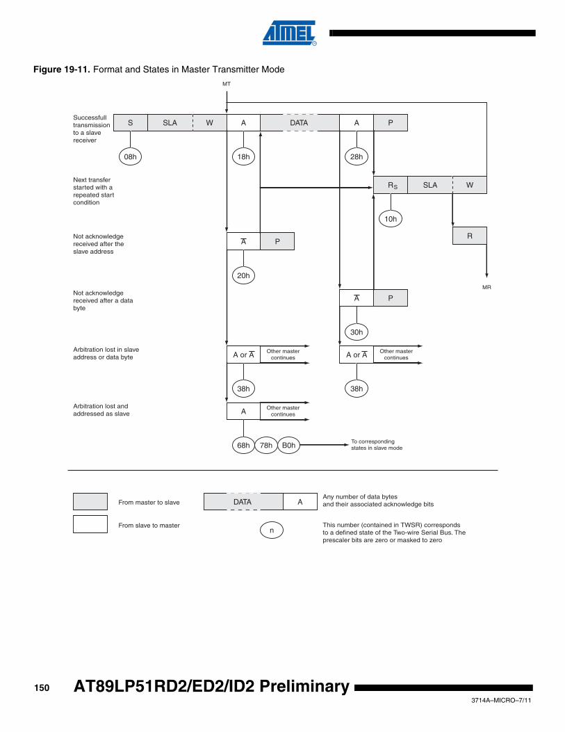
Figure 19-11. Format and States in Master Transmitter Mode
S SLA W A DATA A P
08h 18h 28h
R SLA W
10h
A P
20h
P
30h
A or A
38h
A
Other mastercontinues A or A
38h
Other mastercontinues
R
A
68h
Other mastercontinues
78h B0hTo correspondingstates in slave mode
MT
MR
Successfulltransmissionto a slavereceiver
Next transferstarted with arepeated startcondition
Not acknowledgereceived after theslave address
Not acknowledgereceived after a databyte
Arbitration lost in slaveaddress or data byte
Arbitration lost andaddressed as slave
DATA A
n
From master to slave
From slave to master
Any number of data bytesand their associated acknowledge bits
This number (contained in TWSR) correspondsto a defined state of the Two-wire Serial Bus. Theprescaler bits are zero or masked to zero
S
1503714A–MICRO–7/11
AT89LP51RD2/ED2/ID2 Preliminary

AT89LP51RD2/ED2/ID2 Preliminary
Table 19-7. Status Codes for Master Receiver Mode
Status Code
(SSCS)
Status of the Two-wire Serial Bus and Two-wire Serial Interface Hardware
Application Software Response
Next Action Taken by TWI HardwareTo/from SSDAT
To SSCON
STA STO SI AA
08hA START condition has been transmitted
Load SLA+R 0 0 1 XSLA+R will be transmitted; ACK or NOT ACK will be received
10hA repeated START condition has been transmitted
Load SLA+R 0 0 1 XSLA+R will be transmitted; ACK or NOT ACK will be received
Load SLA+W 0 0 1 XSLA+W will be transmitted; Logic will switch to Master Transmitter mode
38hArbitration lost in SLA+R or NOT ACK bit
No action 0 0 1 XTwo-wire Serial Bus will be released and not addressed Slave mode will be entered
No action 1 0 1 XA START condition will be transmitted when the bus becomes free
40hSLA+R has been transmitted; ACK has been received
No action 0 0 1 0Data byte will be received and NOT ACK will be returned
No action 0 0 1 1Data byte will be received and ACK will be returned
48hSLA+R has been transmitted; NOT ACK has been received
No action 1 0 1 X Repeated START will be transmitted
No action 0 1 1 XSTOP condition will be transmitted and STO flag will be reset
No action 1 1 1 XSTOP condition followed by a START condition will be transmitted and STO flag will be reset
50hData byte has been received; ACK has been returned
Read data byte 0 0 1 0Data byte will be received and NOT ACK will be returned
Read data byte 0 0 1 1Data byte will be received and ACK will be returned
58hData byte has been received; NOT ACK has been returned
Read data byte 1 0 1 X Repeated START will be transmitted
Read data byte 0 1 1 XSTOP condition will be transmitted and STO flag will be reset
Read data byte 1 1 1 XSTOP condition followed by a START condition will be transmitted and STO flag will be reset
1513714A–MICRO–7/11

Figure 19-12. Format and States in Master Receiver Mode
19.6.3 Slave Receiver ModeIn the Slave Receiver mode, a number of data bytes are received from a master transmitter. Toinitiate the Slave Receiver mode, SSADR and SSCON must be initialized as follows:
The upper seven bits are the address to which the Two-wire Serial Interface will respond whenaddressed by a master. If the LSB is set, the TWI will respond to the general call address (00h),otherwise it will ignore the general call address.:
S SLA R A DATA A
08h 40h 50h
SLA R
10h
A P
48h
A or A
38h
Other mastercontinues
38h
Other mastercontinues
W
A
68h
Other mastercontinues
78h B0hTo correspondingstates in slave mode
MR
MT
Successfullreceptionfrom a slavereceiver
Next transferstarted with arepeated startcondition
Not acknowledgereceived after theslave address
Arbitration lost in slaveaddress or data byte
Arbitration lost andaddressed as slave
DATA A
n
From master to slave
From slave to master
Any number of data bytesand their associated acknowledge bits
This number (contained in TWSR) correspondsto a defined state of the Two-wire Serial Bus. The prescaler bits are zero or masked to zero
PDATA A
58h
A
RS
SSADR S6 SA5 SA4 SA3 SA2 SA1 SA0 GC
Value Device’s own Slave Address X
SSCON CR2 SSIE STA STO SI AA CR1 CR0
Value X 1 0 0 0 1 X X
1523714A–MICRO–7/11
AT89LP51RD2/ED2/ID2 Preliminary

AT89LP51RD2/ED2/ID2 Preliminary
SSIE must be written to one to enable the TWI. The AA bit must be written to one to enable theacknowledgment of the device’s own slave address or the general call address. STA and STOmust be written to zero.
When SSADR and SSCON have been initialized, the TWI waits until it is addressed by its ownslave address (or the general call address if enabled) followed by the data direction bit. If thedirection bit is “0” (write), the TWI will operate in SR mode, otherwise ST mode is entered. Afterits own slave address and the write bit have been received, the SI flag is set and a valid statuscode can be read from SSCS. The status code is used to determine the appropriate softwareaction. The appropriate action to be taken for each status code is detailed in Table 19-8. TheSlave Receiver mode may also be entered if arbitration is lost while the TWI is in the Mastermode (see states 68h and 78h).
If the AA bit is reset during a transfer, the TWI will return a “Not Acknowledge” (“1”) to SDA afterthe next received data byte. This can be used to indicate that the slave is not able to receive anymore bytes. While AA is zero, the TWI does not acknowledge its own slave address. However,the Two-wire Serial Bus is still monitored and address recognition may resume at any time bysetting AA. This implies that the AA bit may be used to temporarily isolate the TWI from the Two-wire Serial Bus.
.
Table 19-8. Status Codes for Slave Receiver Mode
Status Code
(SSCS)
Status of the Two-wire Serial Bus and Two-wire Serial Interface Hardware
Application Software Response
Next Action Taken by TWI HardwareTo/from SSDAT
To SSCON
STA STO SI AA
60hOwn SLA+W has been received; ACK has been returned
No action X 0 1 0Data byte will be received and NOT ACK will be returned
No action X 0 1 1Data byte will be received and ACK will be returned
68h
Arbitration lost in SLA+R/W as master; own SLA+W has been received; ACK has been returned
No action X 0 1 0Data byte will be received and NOT ACK will be returned
No action X 0 1 1Data byte will be received and ACK will be returned
70hGeneral call address has been received; ACK has been returned
No action X 0 1 0Data byte will be received and NOT ACK will be returned
No action X 0 1 1Data byte will be received and ACK will be returned
78h
Arbitration lost in SLA+R/W as master; General call address has been received; ACK has been returned
No action X 0 1 0Data byte will be received and NOT ACK will be returned
No action X 0 1 1Data byte will be received and ACK will be returned
80h
Previously addressed with own SLA+W; data has been received; ACK has been returned
Read data byte X 0 1 0Data byte will be received and NOT ACK will be returned
Read data byte X 0 1 1Data byte will be received and ACK will be returned
1533714A–MICRO–7/11

88h
Previously addressed with own SLA+W; data has been received; NOT ACK has been returned
Read data byte 0 0 1 0Switched to the not addressed Slave mode; no recognition of own SLA or GCA
Read data byte 0 0 1 1Switched to the not addressed Slave mode; own SLA will be recognized; GCA will be recognized if GC = “1”
Read data byte 1 0 1 0
Switched to the not addressed Slave mode; no recognition of own SLA or GCA; a START condition will be transmitted when the bus becomes free
Read data byte 1 0 1 1
Switched to the not addressed Slave mode; own SLA will be recognized; GCA will be recognized if GC = “1”; a START condition will be transmitted when the bus becomes free
90h
Previously addressed with general call; data has been received; ACK has been returned
Read data byte X 0 1 0Data byte will be received and NOT ACK will be returned
Read data byte X 0 1 1Data byte will be received and ACK will be returned
98h
Previously addressed with general call; data has been received; NOT ACK has been returned
Read data byte 0 0 1 0Switched to the not addressed Slave mode; no recognition of own SLA or GCA
Read data byte 0 0 1 1Switched to the not addressed Slave mode; own SLA will be recognized; GCA will be recognized if GC = “1”
Read data byte 1 0 1 0
Switched to the not addressed Slave mode; no recognition of own SLA or GCA; a START condition will be transmitted when the bus becomes free
Read data byte 1 0 1 1
Switched to the not addressed Slave mode; own SLA will be recognized; GCA will be recognized if GC = “1”; a START condition will be transmitted when the bus becomes free
A0h
A STOP condition or repeated START condition has been received while still addressed as slave
No Action 0 0 1 0Switched to the not addressed Slave mode; no recognition of own SLA or GCA
No Action 0 0 1 1Switched to the not addressed Slave mode; own SLA will be recognized; GCA will be recognized if GC = “1”
No Action 1 0 1 0
Switched to the not addressed Slave mode; no recognition of own SLA or GCA; a START condition will be transmitted when the bus becomes free
No Action 1 0 1 1
Switched to the not addressed Slave mode; own SLA will be recognized; GCA will be recognized if GC = “1”; a START condition will be transmitted when the bus becomes free
Table 19-8. Status Codes for Slave Receiver Mode
1543714A–MICRO–7/11
AT89LP51RD2/ED2/ID2 Preliminary

AT89LP51RD2/ED2/ID2 Preliminary
Figure 19-13. Format and States in Slave Receiver Mode
S SLA W A DATA A
60h 80h
88h
A
68h
Reception of the ownslave address and one ormore data bytes. All areacknowledged
Last data byte receivedis not acknowledged
Arbitration lost as masterand addressed as slave
Reception of the general calladdress and one or more databytes
Last data byte received isnot acknowledged
n
From master to slave
From slave to master
Any number of data bytesand their associated acknowledge bits
This number (contained in TWSR) correspondsto a defined state of the Two-wire Serial Bus. The prescaler bits are zero or masked to zero
P or SDATA A
80h A0h
P or SA
A DATA A
70h 90h
98h
A
78h
P or SDATA A
90h A0h
P or SA
General Call
Arbitration lost as master andaddressed as slave by general call
DATA A
1553714A–MICRO–7/11

19.6.4 Slave Transmitter Mode
In the Slave Transmitter mode, a number of data bytes are transmitted to a master receiver. Toinitiate the Slave Transmitter mode, upper 7 bits of SSADR must be initialized with the addressto which the Two-wire Serial Interface will respond when addressed by a master. If the LSB isset, the TWI will respond to the general call address (00h), otherwise it will ignore the generalcall address. SSIE must be written to one to enable the TWI. The AA bit must be written to oneto enable the acknowledgment of the device’s own slave address or the general call address.STA and STO must be written to zero.
When SSADR and SSCON have been initialized, the TWI waits until it is addressed by its ownslave address (or the general call address if enabled) followed by the data direction bit. If thedirection bit is “1” (read), the TWI will operate in ST mode, otherwise SR mode is entered. Afterits own slave address and the write bit have been received, the TWINT flag is set and a validstatus code can be read from SSCS. The status code is used to determine the appropriate soft-ware action. The appropriate action to be taken for each status code is detailed in Table 19-9.The Slave Transmitter mode may also be entered if arbitration is lost while the TWI is in theMaster mode (see state B0h).
If the AA bit is written to zero during a transfer, the TWI will transmit the last byte of the transfer.State C0h or state C8h will be entered, depending on whether the master receiver transmits aNACK or ACK after the final byte. The TWI is switched to the not addressed Slave mode, andwill ignore the master if it continues the transfer. Thus the master receiver receives all “1s” asserial data. State C8h is entered if the master demands additional data bytes (by transmittingACK), even though the slave has transmitted the last byte (AA zero and expecting NACK fromthe master). While AA is zero, the TWI does not respond to its own slave address. However, theTwo-wire Serial Bus is still monitored and address recognition may resume at any time by set-ting AA. This implies that the AA bit may be used to temporarily isolate the TWI from the Two-wire Serial Bus.
Figure 19-14. Format and States in Slave Transmitter Mode
S SLA R A DATA A
A8h B8h
A
B0h
Reception of the ownslave address and one ormore data bytes
Last data byte transmitted.Switched to not addressedslave (TWEA = '0')
Arbitration lost as masterand addressed as slave
n
From master to slave
From slave to master
Any number of data bytesand their associated acknowledge bits
This number (contained in TWSR) correspondsto a defined state of the Two-wire Serial Bus. The prescaler bits are zero or masked to zero
P or SDATA
C0h
DATA A
A
C8h
P or SAll 1's
A
1563714A–MICRO–7/11
AT89LP51RD2/ED2/ID2 Preliminary

AT89LP51RD2/ED2/ID2 Preliminary
.
19.6.5 Miscellaneous StatesThere are two status codes that do not correspond to a defined TWI state, see Table 19-10.
Status F8h indicates that no relevant information is available because the SI flag is not set. Thisoccurs between other states, and when the TWI is not involved in a serial transfer.
Status 00h indicates that a bus error has occurred during a Two-wire Serial Bus transfer. A buserror occurs when a START or STOP condition occurs at an illegal position in the format frame.
Table 19-9. Status Codes for Slave Transmitter Mode
Status Code
(SSCS)
Status of the Two-wire Serial Bus and Two-wire Serial Interface Hardware
Application Software Response
Next Action Taken by TWI HardwareTo/from SSDAT
To SSCON
STA STO SI AA
A8hOwn SLA+R has been received; ACK has been returned
Load data byte X 0 1 0Last data byte will be transmitted and NOT ACK should be received
Load data byte X 0 1 1Data byte will be transmitted and ACK should be received
B0h
Arbitration lost in SLA+R/W as master; own SLA+R has been received; ACK has been returned
Load data byte X 0 1 0Last data byte will be transmitted and NOT ACK should be received
Load data byte X 0 1 1Data byte will be transmitted and ACK should be received
B8hData byte in SSDAT has been transmitted; ACK has been received
Load data byte X 0 1 0Last data byte will be transmitted and NOT ACK should be received
Load data byte X 0 1 1Data byte will be transmitted and ACK should be received
C0hData byte in SSDAT has been transmitted; NOT ACK has been received
No action 0 0 1 0Switched to the not addressed Slave mode; no recognition of own SLA or GCA
No action 0 0 1 1Switched to the not addressed Slave mode; own SLA will be recognized; GCA will be recognized if GC = “1”
No action 1 0 1 0
Switched to the not addressed Slave mode; no recognition of own SLA or GCA; a START condition will be transmitted when the bus becomes free
No action 1 0 1 1
Switched to the not addressed Slave mode; own SLA will be recognized; GCA will be recognized if GC = “1”; a START condition will be transmitted when the bus becomes free
C8hLast data byte in SSDAT has been transmitted (AA = “0”); ACK has been received
No action 0 0 1 0Switched to the not addressed Slave mode; no recognition of own SLA or GCA
No action 0 0 1 1Switched to the not addressed Slave mode; own SLA will be recognized; GCA will be recognized if GC = “1”
No action 1 0 1 0
Switched to the not addressed Slave mode; no recognition of own SLA or GCA; a START condition will be transmitted when the bus becomes free
No action 1 0 1 1
Switched to the not addressed Slave mode; own SLA will be recognized; GCA will be recognized if GC = “1”; a START condition will be transmitted when the bus becomes free
1573714A–MICRO–7/11

Examples of such illegal positions are during the serial transfer of an address byte, a data byte,or an acknowledge bit. When a bus error occurs, SI is set. To recover from a bus error, the STOflag must set and SI must be cleared. This causes the TWI to enter the not addressed Slavemode and to clear the STO flag (no other bits in SSCON are affected). The SDA and SCL linesare released, and no STOP condition is transmitted.
19.6.6 Combining Several TWI ModesIn some cases, several TWI modes must be combined in order to complete the desired action.Consider for example reading data from a serial EEPROM. Typically, such a transfer involvesthe following steps:
1. The transfer must be initiated.
2. The EEPROM must be instructed what location should be read.
3. The reading must be performed.
4. The transfer must be finished.
Note that data is transmitted both from Master to Slave and vice versa. The Master must instructthe Slave what location it wants to read, requiring the use of the MT mode. Subsequently, datamust be read from the Slave, implying the use of the MR mode. Thus, the transfer direction mustbe changed. The Master must keep control of the bus during all these steps, and the stepsshould be carried out as an atomic operation. If this principle is violated in a multi-master sys-tem, another Master can alter the data pointer in the EEPROM between steps 2 and 3, and theMaster will read the wrong data location. Such a change in transfer direction is accomplished bytransmitting a REPEATED START between the transmission of the address byte and receptionof the data. After a REPEATED START, the Master keeps ownership of the bus. The followingfigure shows the flow in this transfer.
Figure 19-15. Combining Several TWI Modes to Access a Serial EEPROM
Table 19-10. Miscellaneous States
Status Code
(SSCS)
Status of the Two-wire Serial Bus and Two-wire Serial Interface hardware
Application Software Response
Next Action Taken by TWI HardwareTo/from SSDAT
To SSCON
STA STO SI AA
F8hNo relevant state information available; SI = “0”
No action No action Wait or proceed current transfer
00hBus error due to an illegal START or STOP condition
No action 0 1 1 XOnly the internal hardware is affected, no STOP condition is sent on the bus. In all cases, the bus is released and STO is cleared.
Master Transmitter Master Receiver
S = START Rs = REPEATED START P = STOP
Transmitted from master to slave Transmitted from slave to master
S SLA+W A ADDRESS A Rs SLA+R A DATA A P
1583714A–MICRO–7/11
AT89LP51RD2/ED2/ID2 Preliminary

AT89LP51RD2/ED2/ID2 Preliminary
20. Dual Analog ComparatorsThe AT89LP51RD2/ED2/ID2 provides two analog comparators. The analog comparators havethe following features:
• Internal 3-level Voltage Reference (1.125V, 1.25V, 1.375V)
• Four Shared Analog Input Channels
– Configure as Multiple Input Window Comparator
• Selectable Interrupt Conditions
– High- or Low-level
– Rising- or Falling-edge
– Output Toggle
• Hardware Debouncing Modes
Figure 20-1. Dual Comparator Block Diagram
A block diagram of the dual analog comparators with relevant connections is shown in Figure20-1. Input options allow the comparators to function in a number of different configurations asshown in Figure 20-4. Comparator operation is such that the output is a logic “1” when the posi-tive input is greater than the negative input. Otherwise the output is a zero. Setting the CENA(ACSRA.3) and CENB (ACSRB.3) bits enable Comparator A and B respectively. The user mustalso set the CONA (ACSRA.5) or CONB (ACSRB.5) bits to connect the comparator inputsbefore using a comparator. When a comparator is first enabled, the comparator output and inter-rupt flag are not guaranteed to be stable for 10 µs. The corresponding comparator interruptshould not be enabled during that time, and the comparator interrupt flag must be cleared beforethe interrupt is enabled in order to prevent an immediate interrupt service.
Before enabling the comparators, the analog inputs should be tristated by putting P2.4, P2.5,P2.6 and P2.7 into input-only mode. See “Port Analog Functions” on page 74. It is not possibleto use the Analog Comparators with external program memory or external data memory with 16-bit addresses (MOVX @DPTR) since these functions require the use of Port 2 for addressing.
A
B
(P2.5) AIN1
(P2.6) AIN2
(P2.4) AIN0
(P2.7) AIN3
11
10
01
00
11
10
01
00
RFB1
RFB0
RFA1
RFA0
11
10
01
00
11
10
01
00
CSB0
CSB1
CSA0
CSA1
CMPB
CMPA
CMB0
CMB1
CMB2
CMA0
CMA1
CMA2
CFB
CFA ECMP
Interrupt
VAREF
VAREF-Δ
VAREF+Δ
1593714A–MICRO–7/11

Each comparator may be configured to cause an interrupt under a variety of output value condi-tions by setting the CMx2-0 bits in ACSRx (See Table 20-1 or Table 20-2). The comparatorinterrupt flags CFx in ACSRx are set whenever the comparator outputs match the conditionsspecified by CMx2-0. The flags may be polled by software or may be used to generate an inter-rupt and must be cleared by software. Both comparators share a common interrupt vector. Ifboth comparators are enabled, the user needs to read the flags after entering the interrupt ser-vice routine to determine which comparator caused the interrupt.
The CCS1-0 bits in AREF (Table 20-3) control when the comparator interrupts sample the com-parator outputs. Normally the outputs are sampled every clock system; however, the outputsmay also be sampled whenever Timer 0, Timer 1 or Timer 2 overflows. These settings allow thecomparators to be sampled at a specific time or to reduce the number of comparator eventsseen by the system when using level sensitive modes. The raw value of the comparator outputscan always be read from the CMPA and CMPB bits in AREF.
The comparators will continue to function during Idle mode. If this is not the desired behavior,the comparators should be disabled before entering Idle. The comparators are always disabledduring Power-down mode.
20.1 Analog Input MuxesThe positive input terminal of each comparator may be connected to any of the four analog inputpins by changing the CSA1-0 or CSB1-0 bits in ACSRA and ACSRB. When changing the analoginput pins, the comparator must be disconnected from its inputs by clearing the CONA or CONBbits. The connection is restored by setting the bits again after the muxes have been modified.
CLR EC ; Disable comparator interrupts
ANL ACSRA, #0DFh ; Clear CONA to disconnect COMP A... ; Modify CSA or RFA bitsORL ACSRA, #020h ; Set CONA to connect COMP A
ANL ACSRA, #0EFh ; Clear any spurious interrupt
SETB EC ; Re-enable comparator interrupts
The corresponding comparator interrupt should not be enabled while the inputs are beingchanged, and the comparator interrupt flag must be cleared before the interrupt is re-enabled inorder to prevent an unintentional interrupt request.
The equivalent model for the analog input circuitry is illustrated in Figure 21-2. An analog sourceapplied to AINn is subjected to the pin capacitance and input leakage of that pin, regardless ofwhether that channel is selected as input to the comparator. When the channel is selected, thesource must drive the input capacitance of the comparator through the series resistance (com-bined resistance in the input path).
Figure 20-2. Equivalent Analog Input Model
AINn
CCMP < 0.3 pF
RIN = 10 kΩ
CPIN = 10 pF
RMUX = 10 kΩ
1603714A–MICRO–7/11
AT89LP51RD2/ED2/ID2 Preliminary

AT89LP51RD2/ED2/ID2 Preliminary
20.2 Internal Reference VoltageThe negative input terminal of each comparator may be connected to an internal voltage refer-ence by changing the RFB1-0 or RFA1-0 bits in AREF. The internal reference voltage, VAREF, isset to 1.25 V ±5%. The voltage reference also provides two additional voltage levels approxi-mately 125 mV above and below VAREF. These levels may be used to configure the comparatorsas an internally referenced window comparator with up to four input channels. Changing the ref-erence input must follow the same routine used for changing the positive input as described in“Analog Input Muxes” above.
20.3 Comparator Interrupt DebouncingThe comparator output is normally sampled every clock cycle. The conditions on the analoginputs may be such that the comparator output will toggle excessively. This is especially true ifapplying slow moving analog inputs. Three debouncing modes are provided to filter out thisnoise for edge-triggered interrupts. In debouncing mode, the comparator uses Timer 1 to modu-late its sampling time when CxC1-0 = 00B. When a relevant transition occurs, the comparatorwaits until two Timer 1 overflows have occurred before resampling the output. If the new sampleagrees with the expected value, CFx is set. Otherwise, the event is ignored. The filter may betuned by adjusting the time-out period of Timer 1. Because Timer 1 is free running, thedebouncer must wait for two overflows to guarantee that the sampling delay is at least 1 time-outperiod. Therefore, after the initial edge event, the interrupt may occur between 1 and 2 time-outperiods later. See Figure 20-3. When the comparator clock is provided by one of the timer over-flows, i.e. CxC1-0 != 00B, any change in the comparator output must be valid after 4 samples tobe accepted as an edge event.
Figure 20-3. Negative Edge with Debouncing Example
When the comparator sampling clock is configured for a timer overflow, Timer 1 still controls thedebouncing. The sampling clock will determine when the edge event occurs and the interrupt willbe validated two Timer 1 overflows after this event. When Timer 1 is selected for the samplingclock, this means the interrupt will occur on the second overflow after the overflow that sampleddesired event.
Comparator Out
Timer 1 Overflow
CFx
Start Start
Compare(rejected)
Compare(accepted)
1613714A–MICRO–7/11

Figure 20-4. Dual Comparator Configuration Examples
a. dual independent comparators with external references
+
-A CMPA
AIN0
AIN1
+
-B CMPB
AIN3
AIN2
CSA = 00 RFA = 00 CSB = 11 RFB = 00
b. 3-channel comparator with external reference
+
-A CMPA
AIN0
AIN1
CSA = 00/10/11 RFA = 00
AIN2
AIN3
c. 4-channel comparator with internal reference
+
-A CMPA
AIN0
VAREF
CSA = 00/01/10/11 RFA = 10
AIN1
AIN2
AIN3
d. 2-channel comparator with internal reference & comparator with external reference
+
-A CMPA
AIN0
VAREF
CSA = 00/01 RFA = 10
AIN1+
-B CMPBAIN3
AIN2
CSB = 11 RFB = 00
e. 2-channel comparator with external reference & comparator with internal reference
+
-A CMPA
AIN0
VAREF
CSA = 00/10 RFA = 00
AIN1
+
-B CMPBAIN2
AIN3
CSB = 11 RFB = 10
+
-B CMPB
+
-A CMPA
AIN1
AIN2
AIN0
AIN3
CSA = CSB = 00/11RFA = RFB = 00
f. 2-channel window comparator with external reference
+
-B CMPB
+
-A CMPAAIN3
AIN0
AIN1
AIN2
CSA = CSB = 00/01/10/11RFA = 01 RFB = 11
g. 4-channel window comparator with internal reference
VAREF+Δ
VAREF-Δ
1623714A–MICRO–7/11
AT89LP51RD2/ED2/ID2 Preliminary
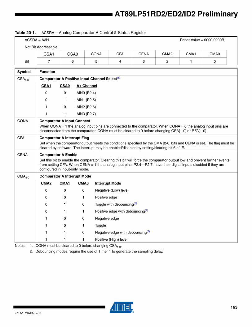
AT89LP51RD2/ED2/ID2 Preliminary
Notes: 1. CONA must be cleared to 0 before changing CSA1-0.
2. Debouncing modes require the use of Timer 1 to generate the sampling delay.
Table 20-1. ACSRA – Analog Comparator A Control & Status Register
ACSRA = A3H Reset Value = 0000 0000B
Not Bit Addressable
CSA1 CSA0 CONA CFA CENA CMA2 CMA1 CMA0
Bit 7 6 5 4 3 2 1 0
Symbol Function
CSA1-0 Comparator A Positive Input Channel Select(1)
CSA1 CSA0 A+ Channel
0 0 AIN0 (P2.4)
0 1 AIN1 (P2.5)
1 0 AIN2 (P2.6)
1 1 AIN3 (P2.7)
CONA Comparator A Input ConnectWhen CONA = 1 the analog input pins are connected to the comparator. When CONA = 0 the analog input pins are disconnected from the comparator. CONA must be cleared to 0 before changing CSA[1-0] or RFA[1-0].
CFA Comparator A Interrupt FlagSet when the comparator output meets the conditions specified by the CMA [2-0] bits and CENA is set. The flag must be cleared by software. The interrupt may be enabled/disabled by setting/clearing bit 6 of IE.
CENA Comparator A EnableSet this bit to enable the comparator. Clearing this bit will force the comparator output low and prevent further events from setting CFA. When CENA = 1 the analog input pins, P2.4—P2.7, have their digital inputs disabled if they are configured in input-only mode.
CMA2-0 Comparator A Interrupt Mode
CMA2 CMA1 CMA0 Interrupt Mode
0 0 0 Negative (Low) level
0 0 1 Positive edge
0 1 0 Toggle with debouncing(2)
0 1 1 Positive edge with debouncing(2)
1 0 0 Negative edge
1 0 1 Toggle
1 1 0 Negative edge with debouncing(2)
1 1 1 Positive (High) level
1633714A–MICRO–7/11
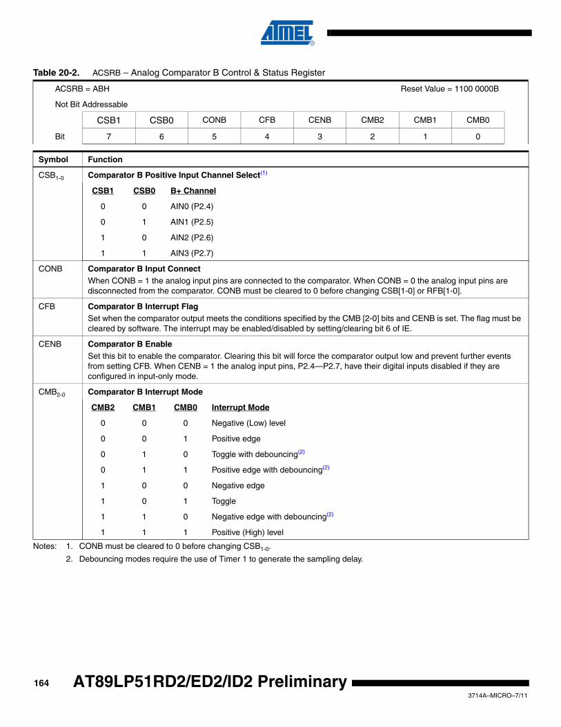
Notes: 1. CONB must be cleared to 0 before changing CSB1-0.
2. Debouncing modes require the use of Timer 1 to generate the sampling delay.
Table 20-2. ACSRB – Analog Comparator B Control & Status Register
ACSRB = ABH Reset Value = 1100 0000B
Not Bit Addressable
CSB1 CSB0 CONB CFB CENB CMB2 CMB1 CMB0
Bit 7 6 5 4 3 2 1 0
Symbol Function
CSB1-0 Comparator B Positive Input Channel Select(1)
CSB1 CSB0 B+ Channel
0 0 AIN0 (P2.4)
0 1 AIN1 (P2.5)
1 0 AIN2 (P2.6)
1 1 AIN3 (P2.7)
CONB Comparator B Input ConnectWhen CONB = 1 the analog input pins are connected to the comparator. When CONB = 0 the analog input pins are disconnected from the comparator. CONB must be cleared to 0 before changing CSB[1-0] or RFB[1-0].
CFB Comparator B Interrupt FlagSet when the comparator output meets the conditions specified by the CMB [2-0] bits and CENB is set. The flag must be cleared by software. The interrupt may be enabled/disabled by setting/clearing bit 6 of IE.
CENB Comparator B EnableSet this bit to enable the comparator. Clearing this bit will force the comparator output low and prevent further events from setting CFB. When CENB = 1 the analog input pins, P2.4—P2.7, have their digital inputs disabled if they are configured in input-only mode.
CMB2-0 Comparator B Interrupt Mode
CMB2 CMB1 CMB0 Interrupt Mode
0 0 0 Negative (Low) level
0 0 1 Positive edge
0 1 0 Toggle with debouncing(2)
0 1 1 Positive edge with debouncing(2)
1 0 0 Negative edge
1 0 1 Toggle
1 1 0 Negative edge with debouncing(2)
1 1 1 Positive (High) level
1643714A–MICRO–7/11
AT89LP51RD2/ED2/ID2 Preliminary
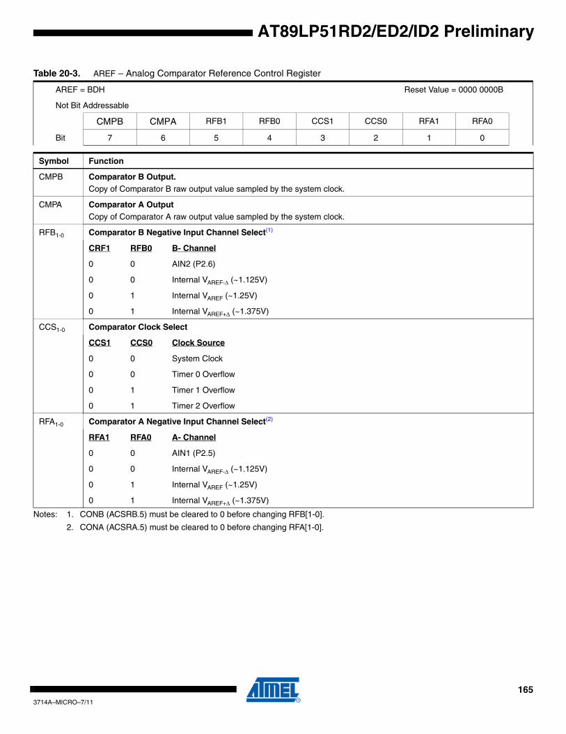
AT89LP51RD2/ED2/ID2 Preliminary
Notes: 1. CONB (ACSRB.5) must be cleared to 0 before changing RFB[1-0].
2. CONA (ACSRA.5) must be cleared to 0 before changing RFA[1-0].
Table 20-3. AREF – Analog Comparator Reference Control Register
AREF = BDH Reset Value = 0000 0000B
Not Bit Addressable
CMPB CMPA RFB1 RFB0 CCS1 CCS0 RFA1 RFA0
Bit 7 6 5 4 3 2 1 0
Symbol Function
CMPB Comparator B Output.Copy of Comparator B raw output value sampled by the system clock.
CMPA Comparator A OutputCopy of Comparator A raw output value sampled by the system clock.
RFB1-0 Comparator B Negative Input Channel Select(1)
CRF1 RFB0 B- Channel
0 0 AIN2 (P2.6)
0 0 Internal VAREF-Δ (~1.125V)
0 1 Internal VAREF (~1.25V)
0 1 Internal VAREF+Δ (~1.375V)
CCS1-0 Comparator Clock Select
CCS1 CCS0 Clock Source
0 0 System Clock
0 0 Timer 0 Overflow
0 1 Timer 1 Overflow
0 1 Timer 2 Overflow
RFA1-0 Comparator A Negative Input Channel Select(2)
RFA1 RFA0 A- Channel
0 0 AIN1 (P2.5)
0 0 Internal VAREF-Δ (~1.125V)
0 1 Internal VAREF (~1.25V)
0 1 Internal VAREF+Δ (~1.375V)
1653714A–MICRO–7/11

21. Digital-to-Analog/Analog-to-Digital ConverterThe AT89LP51RD2/ED2/ID2 includes a 10-bit Data Converter (DADC) with the followingfeatures:
• Digital-to-Analog (DAC) or Analog-to-Digital (ADC) Mode
• 10-bit Resolution
• 6.5 µs Conversion Time
• 7 Multiplexed Single-ended Channels or 3 Differential Channels
• Internal Temperature Sensor or Supply Voltage Channels
• Selectable 1.0V±10% Internal Reference Voltage
• Optional Left-Adjust of Conversion Results
• Single Conversion or Timer-triggered Mode
• Interrupt on Conversion Complete
The AT89LP51RD2/ED2/ID2 features a 10-bit successive approximation data converter thatfunctions in either Analog-to-Digital (ADC) or Digital-to-Analog (DAC) mode. A block diagram ofthe converter is shown in Figure 21-1. An 8-channel Analog Multiplexer connects eight single-ended or four differential voltage inputs from the pins of Port 0 to a sample-and-hold circuit thatin turn provides an input to the successive approximation block. The Sample-and-Hold circuitensures that the input voltage to the ADC is held at a constant level during conversion. The SARblock digitizes the analog voltage into a 10-bit value accessible through a data register. TheSAR block also operates in reverse to generate an analog voltage on Port 2 from a 10-bit digitalvalue.
ADC results are available in the DADL and DADH register pair. The ADC result scale is deter-mined by the reference voltage (VREF) generated either internally from a 1.0V reference orexternally from VDD/2. The ADC results are always represented in signed 2’s complement form,with single-ended voltage channels referring to the level above or below VDD/2. The 10-bitresults may be right or left adjusted within the 16-bit register. The sign is extended through the 6MSBs of right-adjusted results and the 6 LSBs of left-adjusted results are zeroed. If only 8-bitprecision is required, the user should select left-adjusted by setting LADJ in DADC and read onlythe DADH register. Example results are listed in Table 21-1.
The conversion formulas are as follows:
Conversion results can be converted into unsigned binary by adding 02h to DADH in right-adjusted mode or 80h to DADH in left-adjusted mode. When using the external reference(VDD/2) in single-ended mode this is equivalent to:
(Singled-Ended) ADC 511VIN VDD 2⁄( )–
VREF-----------------------------------------×=
(Differential) ADC 511VIN+ VIN-–
VREF----------------------------×=
(Unsigned Singled-Ended) ADC 1023VIN
VDD-----------×=
1663714A–MICRO–7/11
AT89LP51RD2/ED2/ID2 Preliminary

AT89LP51RD2/ED2/ID2 Preliminary
To convert the unsigned binary value back to 2’s complement, subtract 02h from DADH in right-adjusted mode or 80h from DADH in left-adjusted mode. Note that the DADH/DADL registerscannot be directly manipulated as they are read-only in ADC mode and write-only in DAC mode.
Figure 21-1. DADC Block Diagram
8-BIT DATA BUS
15 0 ADC INPUT SELECT
REGISTER (DADI) ADC CTRL & STATUS
REGISTER (DADC) ADC DATA REGISTER
(DADH/DADL)
AC
S2
DA
C
AD
IF
AC
S1
AC
S0
AC
K0
AC
K1
AC
K2
DIF
F
10-BIT SAR
SAMPLE & HOLD
INTERNAL1.0V
REFERENCE
AC
ON
VDD
P0.6
P0.5
P0.4
P0.3
P0.2
P0.1
P0.0
IRE
F
+
-
CHANNEL SELECTION PRESCALER
GND
POS. INPUT MUX
NEG. INPUT MUX
TRIGGER SELECT
Timer Overflows
INTERRUPT FLAG
START
VDD/2
DA+
DA-
TR
G1
TR
G0
GO
AD
CE
LAD
J
VREF
VIN+
VIN-
R
R
VD
D/2
IRE
F
7R
R
VDD/8
VDD/8TEMP
1673714A–MICRO–7/11

21.1 ADC OperationThe ADC converts an analog input voltage to a 10-bit signed digital value through successiveapproximation. When DIFF (DADI.3) is zero, the ADC operates in single-ended mode and theinput voltage is the difference between the voltage at the input pin and VDD/2. In differentialmode (DIFF = 1) the input voltage is the difference between the positive and negative input pins.The minimum value represents zero difference and the maximum values represent a differenceof positive or negative VREF minus 1 LSB.
The analog input channel is selected by writing to the ACS bits in DADI. The first six Port 0 inputpins can be selected as single-ended inputs to the ADC. Three pairs of Port 0 pins can beselected as differential inputs.The ACON bit (DADI.7) must be set to one to connect the inputpins to the ADC. Prior to changing ACS, ACON must be cleared to zero. This ensures thatcrosstalk between channels is limited. ACON must be set back to one after ACS is updated.ACON and ACS should not be changed while a conversion is in progress. ADC input channelsmust have their port pins configured for input-only mode. The AT89LP51RD2/ED2/ID2 alsoincludes an on-chip temperature sensor and voltage supply channel. These features areavailable when ACS = 6. See Section 21.2.
The equivalent model for the analog input circuitry is illustrated in Figure 21-2. An analog sourceapplied to ADCn is subjected to the pin capacitance and input leakage of that pin, regardless ofwhether that channel is selected as input to the ADC. When the channel is selected, the sourcemust drive the S/H capacitor through the series resistance (combined resistance in the inputpath). To achieve 10-bit resolution the S/H capacitor must be charged to within 1/2 LSB of theexpected value within the 1 ADC clock period sample time. High impedance sources mayrequire a reduction in the ADC clock frequency to achieve full resolution.
Figure 21-2. Equivalent Analog Input Model
The ADC is enabled by setting the ADCE bit in DADC. Some settling time is required for the ref-erence circuits to stabilize after the ADC is enabled. The ADC does not consume power whenADCE is cleared, so it is recommended to switch off the ADC before entering power savingmodes.
Table 21-1. Example ADC Conversion Codes
Right Adjust Left Adjust Single-Ended Mode (VIN) Differential Mode (VIN+ – VIN-)
0 0 VDD/2 0
0100h 4000h VDD/2 + 1/2 x VREF 1/2 x VREF
01FFh 7FC0h VDD/2 + 511/512 x VREF 511/512 x VREF
FF00h C000h VDD/2 – 1/2 x VREF –1/2 x VREF
FE01h 8040h VDD/2 – 511/512 x VREF –511/512 x VREF
ADCn
CS/H = 2 pF
RIN =10 kΩ
CPIN = 10 pF
RMUX =10 kΩ
1683714A–MICRO–7/11
AT89LP51RD2/ED2/ID2 Preliminary

AT89LP51RD2/ED2/ID2 Preliminary
A timing diagram of an ADC conversion is shown in Figure 21-3. The conversion requires 13ADC clock cycles to complete. The analog input is sampled during the third cycle of the conver-sion and is held constant for the remainder of the conversion. At the end of the conversion, theinterrupt flag, ADIF, is set and the result is written to the data registers. An additional 1 ADCclock cycle and up to 2 system clock cycles may be required to synchronize ADIF with the rest ofthe system. The results in DADH/DADL remain valid until the next conversion completes. DADHand DADL are read-only registers during ADC mode.
Figure 21-3. ADC Timing Diagram
21.2 Temperature SensorADC input channel 6 is not connected to a port pin. Instead it has a connection to two internalspecial functions: a temperature sensor and a voltage supply monitor. When ACS = 6 the IREFbit in DADI selects between them, such that IREF = 0 selects the voltage supply channel andIREF = 1 select the temperature sensor channel. Both these modes use the internal 1.0V refer-ence for the full scale and the negative input. The temperature sensor outputs a voltage that isproportional to the ambient operating temperature. The uncalibrated output is linear and is suit-able for relative temperature measurements. The supply voltage channel is the device supplylevel divided-by-8. It can be used to find the actual operating voltage of the device.
The following conversion formulae apply for temperature sensor and supply monitor modes:
21.3 DAC OperationThe DAC converts a 10-bit signed digital value to an analog output voltage through successiveapproximation. The DAC always operates in differential mode, outputting a voltage differentialbetween its positive (P2.2) and negative (P2.3) outputs with a common mode of VDD/2. The min-imum value represents zero difference and the maximum values represent a difference ofpositive or negative VREF minus 1 LSB.
The DAC is enabled by setting the ADCE and DAC bits in DADC. Some settling time is requiredfor the reference circuits to stabilize after the DAC is enabled. The DAC does not have multiple
1 2 3 4 5 6 7 8 9 10 11 12 13
MSB of Result
LSB of Result
ADC Clock
GO/BSY
ADIF
DADH
DADL
Cycle Number 1 2
One Conversion Next Conversion
3
Sample & Hold
Initialize CircuitryConversion
Complete Initialize
(Temp Sensor) ADC 511VTEMP VREF–
VREF-------------------------------------×=
(Supply Voltage) ADC 511VDD 8⁄( ) VREF–
VREF------------------------------------------------×=
1693714A–MICRO–7/11

output channels and the DIFF, ACON and ACS bits have no effect in DAC mode. P2.2 and P2.3are automatically forced to input-only mode while the DAC is enabled.
A timing diagram of a DAC conversion is shown in Figure 21-4. The conversion requires 11 ADCclock cycles to complete. Construction of the analog output starts in the second cycle of the con-version and the DAC will allow the new value to propagate to the outputs during cycle 7, after the5 MSBs are complete. At the end of the conversion, the interrupt flag is set. An additional 1 ADCclock cycle and up to 2 system clock cycles may be required to synchronize ADIF with the rest ofthe system. The DADL and DADH registers hold the value to be output and are write-only duringDAC mode. An internal buffer samples DADH/DADL at the start of the conversion and holds thevalue constant for the remainder of the conversion. One system clock cycle is required to trans-fer the contents of DADH/DADL into the buffer at the start of the conversion and therefore theADC clock frequency must always be equal to or less than the system clock frequency duringDAC mode to ensure that the buffer is updated before the second cycle.
Figure 21-4. DAC Timing Diagram
The equivalent model for the analog output circuitry is illustrated in Figure 21-5. The series out-put resistance of the DAC must drive the pin capacitance and any external load on the pin.
Figure 21-5. Equivalent Analog Output Model
21.4 Clock SelectionThe DADC requires a clock of 2 MHz or less to achieve full resolution. By default the DADC willuse an internal 2 MHz clock generated from the 8 MHz internal oscillator. The internal oscillatorwill be enabled even if it is not supplying the system clock. This may result in higher power con-sumption. Conversely, the DADC clock can be generated directly from the system oscillatorusing a 7-bit prescaler. The prescaler output is controlled by the ACK bits in DADC as shown inFigure 21-6. The prescaler is independent of any X2 or CKRL division used for the CPU clock.
1 2 3 4 5 6 7 8 9 10 11
MSB of Output
LSB of Output
ADC Clock
GO/BSY
ADIF
DADH
DADL
Cycle Number 1 2
One Conversion Next Conversion
3
Begin Output
Initialize CircuitryConversion
CompleteInitialize
DAn
VOUT
ROUT =100 kΩ
CPIN = 10 pF
AVDD/2
1703714A–MICRO–7/11
AT89LP51RD2/ED2/ID2 Preliminary

AT89LP51RD2/ED2/ID2 Preliminary
In ADC mode, there are no requirements on the clock frequency with respect to the systemclock. The ADC prescaler selection is independent of the system clock divider and the ADC mayoperate at both higher or lower frequencies than the CPU. However, in DAC mode the ADCclock frequency must not be higher than the CPU clock, including any clock division from thesystem clock.
Figure 21-6. DADC Clock Selection
21.5 Starting a ConversionSetting the GO/BSY bit (DADC.6) when ADCE = 1 starts a single conversion in both ADC andDAC modes. The bit remains set while the conversion is in progress and is cleared by hardwarewhen the conversion completes. The ADC channel should not be changed while a conversion isin progress.
Alternatively, a conversion can be started automatically by various timer sources. Conversiontrigger sources are selected by the TRG bits in DADI. A conversion is started every time theselected timer overflows, allowing for conversions to occur at fixed intervals. The GO/BSY bit willbe set by hardware while the conversion is in progress. Note that the timer overflow rate must beslower than the conversion time.
21.6 Noise ConsiderationsDigital circuitry inside and outside the device generates EMI which might affect the accuracy ofanalog measurements. If conversion accuracy is critical, the noise level can be reduced byapplying the following techniques:
• Keep analog signal paths as short as possible. Make sure to run analog signals tracks over an analog ground plane, and keep them well away from high-speed digital tracks.
• Place the CPU in Idle during a conversion. For best results, use a Timer to start the conversion while CPU is already in Idle Mode.
• If any Port 0 pins are used as digital outputs, it is essential that these do not switch while a conversion is in progress.
7-BIT ADC PRESCALER
ADC CLOCK SOURCE
OSC
ACK0 ACK1 ACK2
CK
/128
CK
/2
CK
/4
CK
/8
CK
/16
CK
/32
CK
/64
INTERNAL 8MHz OSC
÷ 4
1713714A–MICRO–7/11
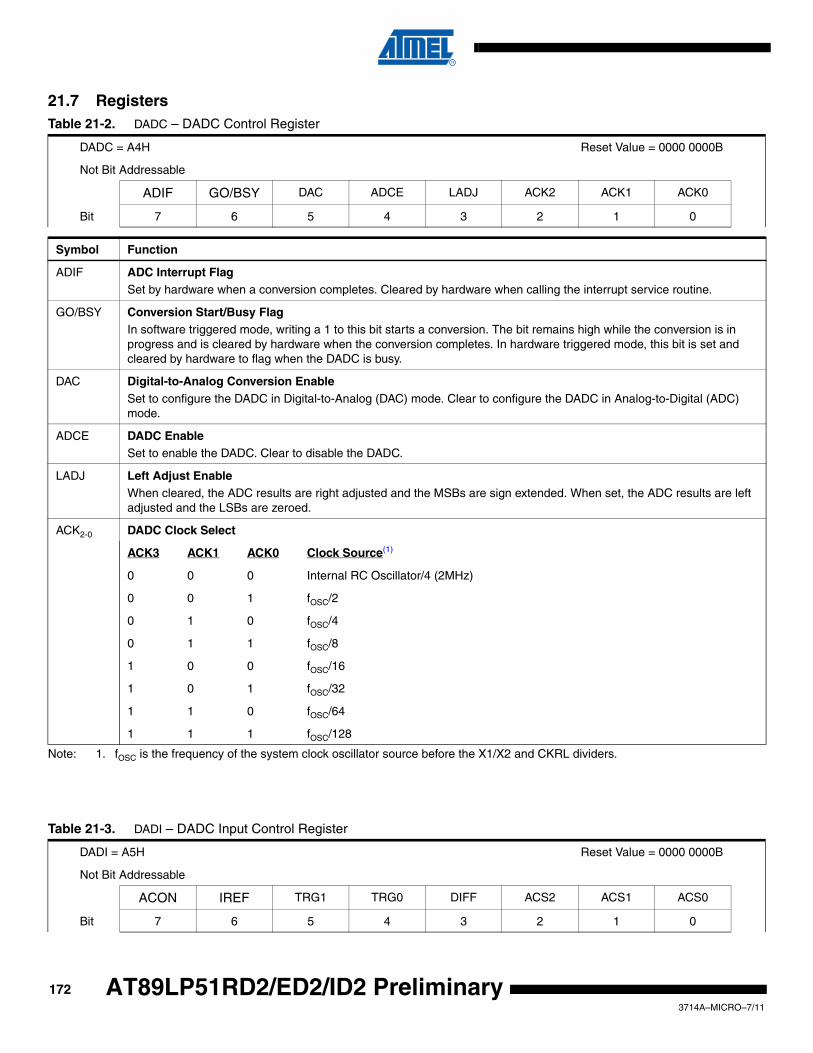
21.7 Registers
Note: 1. fOSC is the frequency of the system clock oscillator source before the X1/X2 and CKRL dividers.
Table 21-2. DADC – DADC Control Register
DADC = A4H Reset Value = 0000 0000B
Not Bit Addressable
ADIF GO/BSY DAC ADCE LADJ ACK2 ACK1 ACK0
Bit 7 6 5 4 3 2 1 0
Symbol Function
ADIF ADC Interrupt FlagSet by hardware when a conversion completes. Cleared by hardware when calling the interrupt service routine.
GO/BSY Conversion Start/Busy FlagIn software triggered mode, writing a 1 to this bit starts a conversion. The bit remains high while the conversion is in progress and is cleared by hardware when the conversion completes. In hardware triggered mode, this bit is set and cleared by hardware to flag when the DADC is busy.
DAC Digital-to-Analog Conversion EnableSet to configure the DADC in Digital-to-Analog (DAC) mode. Clear to configure the DADC in Analog-to-Digital (ADC) mode.
ADCE DADC EnableSet to enable the DADC. Clear to disable the DADC.
LADJ Left Adjust EnableWhen cleared, the ADC results are right adjusted and the MSBs are sign extended. When set, the ADC results are left adjusted and the LSBs are zeroed.
ACK2-0 DADC Clock Select
ACK3 ACK1 ACK0 Clock Source(1)
0 0 0 Internal RC Oscillator/4 (2MHz)
0 0 1 fOSC/2
0 1 0 fOSC/4
0 1 1 fOSC/8
1 0 0 fOSC/16
1 0 1 fOSC/32
1 1 0 fOSC/64
1 1 1 fOSC/128
Table 21-3. DADI – DADC Input Control Register
DADI = A5H Reset Value = 0000 0000B
Not Bit Addressable
ACON IREF TRG1 TRG0 DIFF ACS2 ACS1 ACS0
Bit 7 6 5 4 3 2 1 0
1723714A–MICRO–7/11
AT89LP51RD2/ED2/ID2 Preliminary
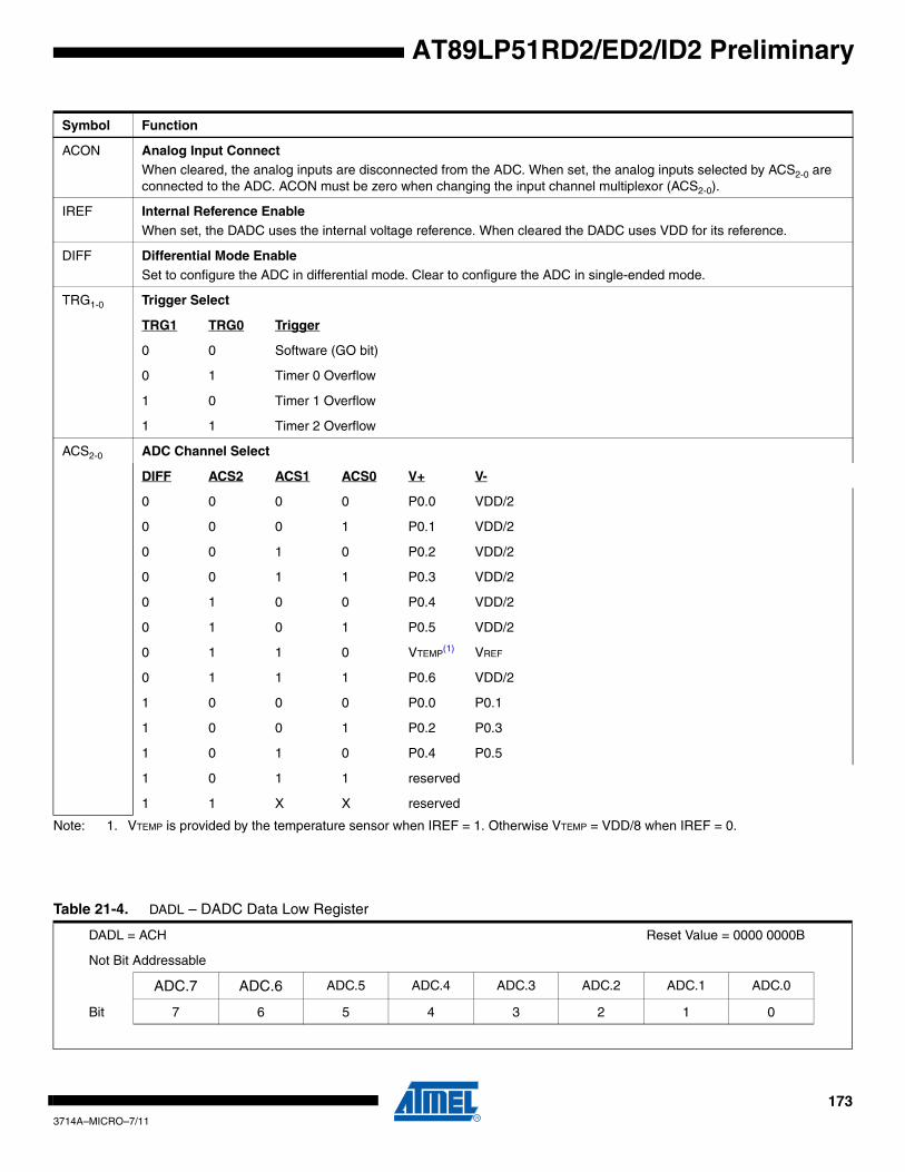
AT89LP51RD2/ED2/ID2 Preliminary
Note: 1. VTEMP is provided by the temperature sensor when IREF = 1. Otherwise VTEMP = VDD/8 when IREF = 0.
Symbol Function
ACON Analog Input ConnectWhen cleared, the analog inputs are disconnected from the ADC. When set, the analog inputs selected by ACS2-0 are connected to the ADC. ACON must be zero when changing the input channel multiplexor (ACS2-0).
IREF Internal Reference EnableWhen set, the DADC uses the internal voltage reference. When cleared the DADC uses VDD for its reference.
DIFF Differential Mode EnableSet to configure the ADC in differential mode. Clear to configure the ADC in single-ended mode.
TRG1-0 Trigger Select
TRG1 TRG0 Trigger
0 0 Software (GO bit)
0 1 Timer 0 Overflow
1 0 Timer 1 Overflow
1 1 Timer 2 Overflow
ACS2-0 ADC Channel Select
DIFF ACS2 ACS1 ACS0 V+ V-
0 0 0 0 P0.0 VDD/2
0 0 0 1 P0.1 VDD/2
0 0 1 0 P0.2 VDD/2
0 0 1 1 P0.3 VDD/2
0 1 0 0 P0.4 VDD/2
0 1 0 1 P0.5 VDD/2
0 1 1 0 VTEMP(1) VREF
0 1 1 1 P0.6 VDD/2
1 0 0 0 P0.0 P0.1
1 0 0 1 P0.2 P0.3
1 0 1 0 P0.4 P0.5
1 0 1 1 reserved
1 1 X X reserved
Table 21-4. DADL – DADC Data Low Register
DADL = ACH Reset Value = 0000 0000B
Not Bit Addressable
ADC.7 ADC.6 ADC.5 ADC.4 ADC.3 ADC.2 ADC.1 ADC.0
Bit 7 6 5 4 3 2 1 0
1733714A–MICRO–7/11

Note: When LADJ = 0, bits 7–0 of the ADC result are found in bits 7–0 of DADL. When LADJ = 1, bits 1–0 of the ADC result are found in bits 7–6 of DADL. Bits 5–0 are cleared to zero.
Note: When LADJ = 0, bits 9–8 of the ADC result are found in bits 1–0 of DADH. Bits 7–2 are signed extended copies of bit 1.When LADJ = 1, bits 9–2 of the ADC result are found in bits 7–0 of DADH.
Table 21-5. DADH – DADC Data High Register
DADH = ADH Reset Value = 0000 0000B
Not Bit Addressable
ADC.15 ADC.14 ADC.13 ADC.12 ADC.11 ADC.10 ADC.9 ADC.8
Bit 7 6 5 4 3 2 1 0
1743714A–MICRO–7/11
AT89LP51RD2/ED2/ID2 Preliminary
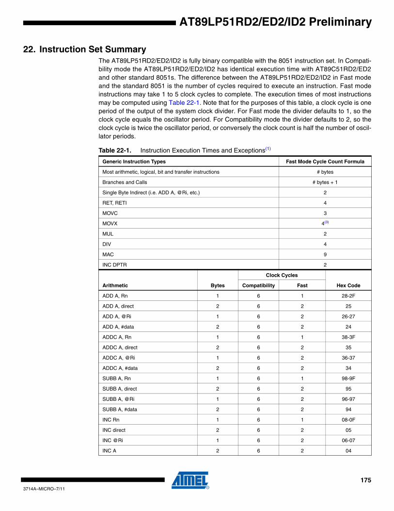
AT89LP51RD2/ED2/ID2 Preliminary
22. Instruction Set SummaryThe AT89LP51RD2/ED2/ID2 is fully binary compatible with the 8051 instruction set. In Compati-bility mode the AT89LP51RD2/ED2/ID2 has identical execution time with AT89C51RD2/ED2and other standard 8051s. The difference between the AT89LP51RD2/ED2/ID2 in Fast modeand the standard 8051 is the number of cycles required to execute an instruction. Fast modeinstructions may take 1 to 5 clock cycles to complete. The execution times of most instructionsmay be computed using Table 22-1. Note that for the purposes of this table, a clock cycle is oneperiod of the output of the system clock divider. For Fast mode the divider defaults to 1, so theclock cycle equals the oscillator period. For Compatibility mode the divider defaults to 2, so theclock cycle is twice the oscillator period, or conversely the clock count is half the number of oscil-lator periods.
Table 22-1. Instruction Execution Times and Exceptions(1)
Generic Instruction Types Fast Mode Cycle Count Formula
Most arithmetic, logical, bit and transfer instructions # bytes
Branches and Calls # bytes + 1
Single Byte Indirect (i.e. ADD A, @Ri, etc.) 2
RET, RETI 4
MOVC 3
MOVX 4(3)
MUL 2
DIV 4
MAC 9
INC DPTR 2
Arithmetic Bytes
Clock Cycles
Hex CodeCompatibility Fast
ADD A, Rn 1 6 1 28-2F
ADD A, direct 2 6 2 25
ADD A, @Ri 1 6 2 26-27
ADD A, #data 2 6 2 24
ADDC A, Rn 1 6 1 38-3F
ADDC A, direct 2 6 2 35
ADDC A, @Ri 1 6 2 36-37
ADDC A, #data 2 6 2 34
SUBB A, Rn 1 6 1 98-9F
SUBB A, direct 2 6 2 95
SUBB A, @Ri 1 6 2 96-97
SUBB A, #data 2 6 2 94
INC Rn 1 6 1 08-0F
INC direct 2 6 2 05
INC @Ri 1 6 2 06-07
INC A 2 6 2 04
1753714A–MICRO–7/11
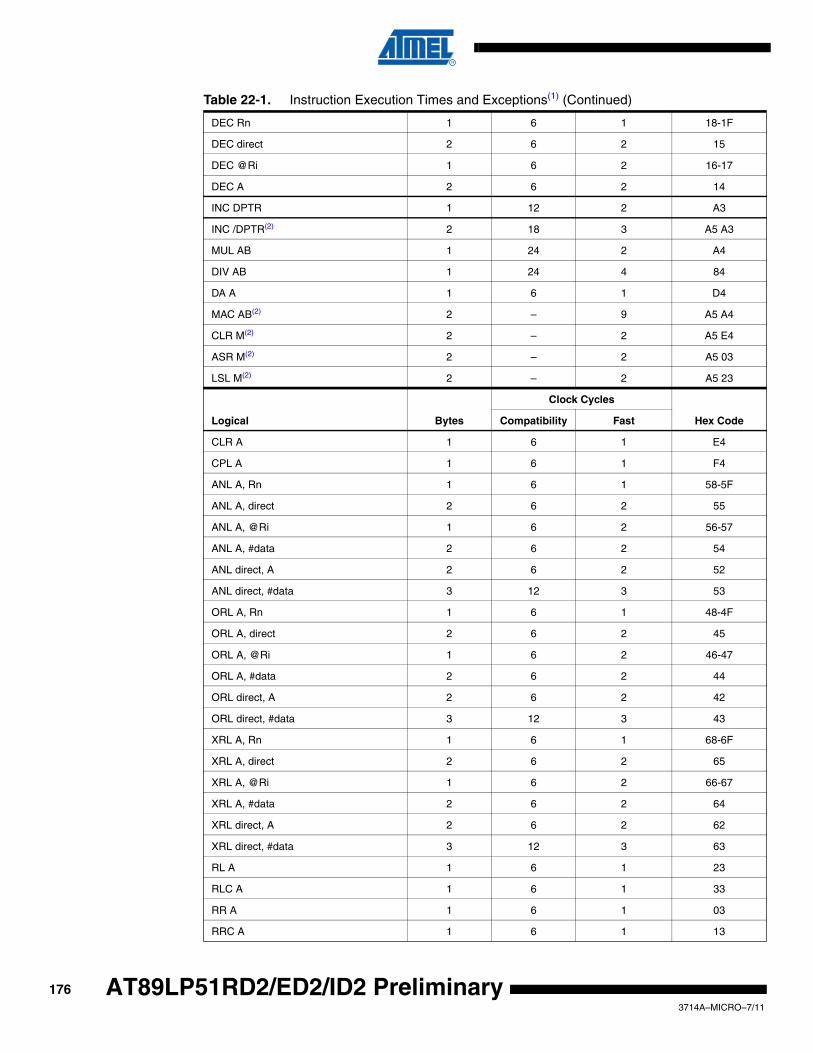
DEC Rn 1 6 1 18-1F
DEC direct 2 6 2 15
DEC @Ri 1 6 2 16-17
DEC A 2 6 2 14
INC DPTR 1 12 2 A3
INC /DPTR(2) 2 18 3 A5 A3
MUL AB 1 24 2 A4
DIV AB 1 24 4 84
DA A 1 6 1 D4
MAC AB(2) 2 – 9 A5 A4
CLR M(2) 2 – 2 A5 E4
ASR M(2) 2 – 2 A5 03
LSL M(2) 2 – 2 A5 23
Logical Bytes
Clock Cycles
Hex CodeCompatibility Fast
CLR A 1 6 1 E4
CPL A 1 6 1 F4
ANL A, Rn 1 6 1 58-5F
ANL A, direct 2 6 2 55
ANL A, @Ri 1 6 2 56-57
ANL A, #data 2 6 2 54
ANL direct, A 2 6 2 52
ANL direct, #data 3 12 3 53
ORL A, Rn 1 6 1 48-4F
ORL A, direct 2 6 2 45
ORL A, @Ri 1 6 2 46-47
ORL A, #data 2 6 2 44
ORL direct, A 2 6 2 42
ORL direct, #data 3 12 3 43
XRL A, Rn 1 6 1 68-6F
XRL A, direct 2 6 2 65
XRL A, @Ri 1 6 2 66-67
XRL A, #data 2 6 2 64
XRL direct, A 2 6 2 62
XRL direct, #data 3 12 3 63
RL A 1 6 1 23
RLC A 1 6 1 33
RR A 1 6 1 03
RRC A 1 6 1 13
Table 22-1. Instruction Execution Times and Exceptions(1) (Continued)
1763714A–MICRO–7/11
AT89LP51RD2/ED2/ID2 Preliminary

AT89LP51RD2/ED2/ID2 Preliminary
SWAP A 1 6 1 C4
Data Transfer Bytes
Clock Cycles
Hex CodeCompatibility Fast
MOV A, Rn 1 6 1 E8-EF
MOV A, direct 2 6 2 E5
MOV A, @Ri 1 6 2 E6-E7
MOV A, #data 2 6 2 74
MOV Rn, A 1 6 1 F8-FF
MOV Rn, direct 2 12 2 A8-AF
MOV Rn, #data 2 6 2 78-7F
MOV direct, A 2 6 2 F5
MOV direct, Rn 2 12 2 88-8F
MOV direct, direct 3 12 3 85
MOV direct, @Ri 2 12 2 86-87
MOV direct, #data 3 12 3 75
MOV @Ri, A 1 6 1 F6-F7
MOV @Ri, direct 2 12 2 A6-A7
MOV @Ri, #data 2 6 2 76-77
MOV DPTR, #data16 3 12 3 90
MOV /DPTR, #data16(2) 4 – 4 A5 90
MOVC A, @A+DPTR 1 12 3 93
MOVC A, @A+/DPTR(2) 2 – 4 A5 93
MOVC A, @A+PC 1 12 3 83
MOVX A, @Ri 1 12 2 E2-E3
MOVX A, @DPTR 1 12(3) 4(3) E0
MOVX A, @/DPTR(2) 2 18(3) 5(3) A5 E0
MOVX @Ri, A 1 12 2 F2-F3
MOVX @DPTR, A 1 12(3) 4(3) F0
MOVX @/DPTR, A(2) 2 18(3) 5(3) A5 F0
PUSH direct 2 12 2 C0
POP direct 2 12 2 D0
XCH A, Rn 1 6 1 C8-CF
XCH A, direct 2 6 2 C5
XCH A, @Ri 1 6 2 C6-C7
XCHD A, @Ri 1 6 2 D6-D7
Bit Operations Bytes
Clock Cycles
Hex CodeCompatibility Fast
CLR C 1 6 1 C3
CLR bit 2 6 2 C2
Table 22-1. Instruction Execution Times and Exceptions(1) (Continued)
1773714A–MICRO–7/11
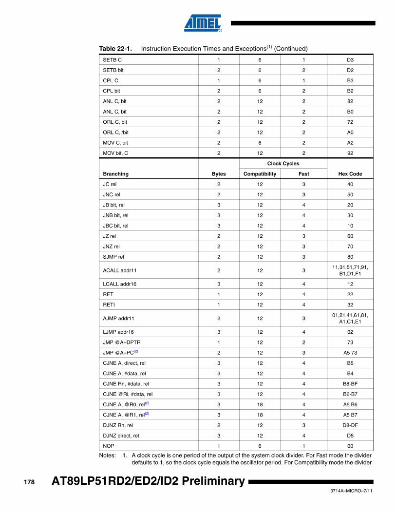
Notes: 1. A clock cycle is one period of the output of the system clock divider. For Fast mode the divider defaults to 1, so the clock cycle equals the oscillator period. For Compatibility mode the divider
SETB C 1 6 1 D3
SETB bit 2 6 2 D2
CPL C 1 6 1 B3
CPL bit 2 6 2 B2
ANL C, bit 2 12 2 82
ANL C, bit 2 12 2 B0
ORL C, bit 2 12 2 72
ORL C, /bit 2 12 2 A0
MOV C, bit 2 6 2 A2
MOV bit, C 2 12 2 92
Branching Bytes
Clock Cycles
Hex CodeCompatibility Fast
JC rel 2 12 3 40
JNC rel 2 12 3 50
JB bit, rel 3 12 4 20
JNB bit, rel 3 12 4 30
JBC bit, rel 3 12 4 10
JZ rel 2 12 3 60
JNZ rel 2 12 3 70
SJMP rel 2 12 3 80
ACALL addr11 2 12 311,31,51,71,91,
B1,D1,F1
LCALL addr16 3 12 4 12
RET 1 12 4 22
RETI 1 12 4 32
AJMP addr11 2 12 301,21,41,61,81,
A1,C1,E1
LJMP addr16 3 12 4 02
JMP @A+DPTR 1 12 2 73
JMP @A+PC(2) 2 12 3 A5 73
CJNE A, direct, rel 3 12 4 B5
CJNE A, #data, rel 3 12 4 B4
CJNE Rn, #data, rel 3 12 4 B8-BF
CJNE @Ri, #data, rel 3 12 4 B6-B7
CJNE A, @R0, rel(2) 3 18 4 A5 B6
CJNE A, @R1, rel(2) 3 18 4 A5 B7
DJNZ Rn, rel 2 12 3 D8-DF
DJNZ direct, rel 3 12 4 D5
NOP 1 6 1 00
Table 22-1. Instruction Execution Times and Exceptions(1) (Continued)
1783714A–MICRO–7/11
AT89LP51RD2/ED2/ID2 Preliminary

AT89LP51RD2/ED2/ID2 Preliminary
defaults to 2, so the clock cycle is twice the oscillator period, or conversely the clock count is half the number of oscillator periods.
2. This escaped instruction is an extension to the instruction set.
3. This is the minimum time for MOVX with no wait states. In Compatibility mode an additional 24 clocks are added for the wait state. In Fast mode, 1 clock is added for each wait state (0–3).
22.1 Instruction Set ExtensionsThe following instructions are extensions to the standard 8051 instruction set that provideenhanced capabilities not found in standard 8051 devices. All extended instructions start with anA5H escape code. For this reason random A5H reserved codes should not be placed in theinstruction stream even though other devices may have treated these as NOPs.
Other AT89LP devices may not support all of these instructions.
22.1.1 ASR M
Function: Shift MAC Accumulator Right Arithmetically
Description: The forty bits in the M register are shifted one bit to the right. Bit 39 retains its value to preserve the sign of the value. No flags are affected.
Example: The M register holds the value 0C5B1A29384H . The following instruction,
ASR M
leaves the M register holding the value 0E2D8D149C2H.
Bytes: 2
Cycles: 2
Encoding: A5 0 0 0 0 0 0 1 1
Operation: ASR(Mn) ← (Mn + 1) n = 0 - 38(M39) ← (M39)
22.1.2 BREAK
Function: Software Breakpoint (Halt execution)
Description: BREAK transfers control from normal execution to the On-Chip Debug (OCD) handler if OCD is enabled. The PC is left pointing to the following instruction. If OCD is disabled, BREAK acts as a double NOP. No flags are affected.
Example: If On-Chip Debugging is allowed, the following instruction,
BREAK
will halt instruction execution prior to the immediately following instruction. If debugging is not allowed, the BREAK is treated as a double NOP.
Bytes: 2
Cycles: 2
Encoding: A5 0 0 0 0 0 0 0 0
Operation: BREAK(PC) ← (PC) + 2
1793714A–MICRO–7/11

22.1.3 CJNE A, @Ri, rel
Function: Compare and Jump if Not Equal
Description: CJNE compares the magnitudes of the Accumulator and indirect RAM location and branches if their values are not equal. The branch destination is computed by adding the signed relative-displacement in the last instruction byte to the PC, after incrementing the PC to the start of the next instruction. The carry flag is set if the unsigned integer value of ACC is less than the unsigned integer value of the indirect location; otherwise, the carry is cleared. Neither operand is affected.
Example: The Accumulator contains 34H. Register 0 contains 78H and 78H contains 56H. The first instruction in the sequence,
CJNE A, @R0, NOT_EQ; . . . . . . ...... ...... ; ACC = @R0.NOT_EQ:
JC REQ_LOW .. ;IF ACC< @R0.; . . . . . . ...... ...... ;ACC > @R0.
sets the carry flag and branches to the instruction at label NOT_EQ. By testing the carry flag, the second instruction determines whether ACC is greater or less than the location pointed to by R0.
Bytes: 2
Cycles: 9
Encoding: A5 1 0 1 1 0 1 1 i rel. address
Operation: CJNE(PC) ← (PC) + 3IF (A) ≠ ((Ri))THEN
(PC) ← (PC) + relative offsetIF (A) < ((Ri))THEN
(C) ← 1ELSE
(C) ← 0
22.1.4 CLR M
Function: Clear MAC Accumulator
Description: CLR M clears the 40-bit M register. No flags are affected.
Example: The M registercontains 123456789AH. The following instruction,
CLR M
leaves the M register set to 0000000000H.
Bytes: 2
Cycles: 2
Encoding: A5 1 1 1 0 0 1 0 0
Operation: JMP(M) ← 0
1803714A–MICRO–7/11
AT89LP51RD2/ED2/ID2 Preliminary

AT89LP51RD2/ED2/ID2 Preliminary
22.1.5 INC /DPTR
Function: Increment Alternate Data Pointer
Description: INC /DPTR increments the unselected 16-bit data pointer by 1. A 16-bit increment (modulo 216 ) is performed, and an overflow of the low-order byte of the data pointer from 0FFH to 00H increments the high-order byte. No flags are affected.
Example: Registers DP1H and DP1L contain 12H and 0FEH, respectively, and DPS = 0. The following instruction sequence,
INC /DPTRINC /DPTRINC /DPTR
changes DP1H and DP1L to 13H and 01H.
Bytes: 2
Cycles: 3
Encoding: A5 1 0 1 0 0 0 1 1
Operation: INCIF (DPS) = 0THEN
(DPTR1) ← (DPTR1) + 1ELSE
(DPTR0) ← (DPTR0) + 1
22.1.6 JMP @A+PC
Function: Jump indirect relative to PC
Description: JMP @A+PC adds the eight-bit unsigned contents of the Accumulator to the program counter, which is first incremented by two. This is the address for subsequent instruction fetches. Sixteen-bit addition is performed (modulo 216): a carry-out from the low-order eight bits propagates through the higher-order bits. The Accumulator is not altered. No flags are affected.
Example: An even number from 0 to 6 is in the Accumulator. The following sequence of instructions branches to one of four AJMP instructions in a jump table starting at JMP_TBL.
JMP @A + PCJMP_TBL:
AJMP LABEL0
AJMP LABEL1AJMP LABEL2
AJMP LABEL3
If the Accumulator equals 04H when starting this sequence, execution jumps to label LABEL2. Because AJMP is a 2-byte instruction, the jump instructions start at every other address.
Bytes: 2
Cycles: 3
Encoding: A5 0 1 1 1 0 0 1 1
Operation: JMP(PC) ← (A) + (PC) + 2
1813714A–MICRO–7/11
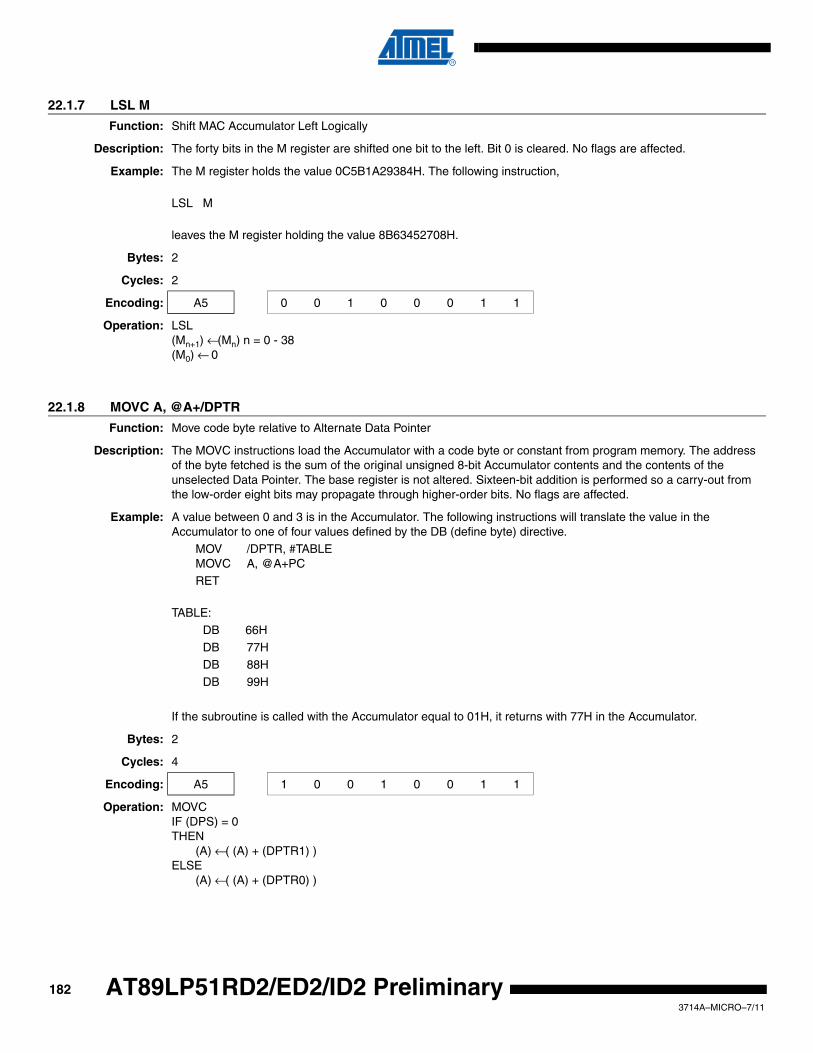
22.1.7 LSL M
Function: Shift MAC Accumulator Left Logically
Description: The forty bits in the M register are shifted one bit to the left. Bit 0 is cleared. No flags are affected.
Example: The M register holds the value 0C5B1A29384H. The following instruction,
LSL M
leaves the M register holding the value 8B63452708H.
Bytes: 2
Cycles: 2
Encoding: A5 0 0 1 0 0 0 1 1
Operation: LSL(Mn+1) ← (Mn) n = 0 - 38(M0) ← 0
22.1.8 MOVC A, @A+/DPTR
Function: Move code byte relative to Alternate Data Pointer
Description: The MOVC instructions load the Accumulator with a code byte or constant from program memory. The address of the byte fetched is the sum of the original unsigned 8-bit Accumulator contents and the contents of the unselected Data Pointer. The base register is not altered. Sixteen-bit addition is performed so a carry-out from the low-order eight bits may propagate through higher-order bits. No flags are affected.
Example: A value between 0 and 3 is in the Accumulator. The following instructions will translate the value in the Accumulator to one of four values defined by the DB (define byte) directive.
MOV /DPTR, #TABLEMOVC A, @A+PCRET
TABLE:
DB 66H
DB 77HDB 88H
DB 99H
If the subroutine is called with the Accumulator equal to 01H, it returns with 77H in the Accumulator.
Bytes: 2
Cycles: 4
Encoding: A5 1 0 0 1 0 0 1 1
Operation: MOVCIF (DPS) = 0THEN
(A) ← ( (A) + (DPTR1) )ELSE
(A) ← ( (A) + (DPTR0) )
1823714A–MICRO–7/11
AT89LP51RD2/ED2/ID2 Preliminary

AT89LP51RD2/ED2/ID2 Preliminary
22.1.9 MAC AB
Function: Multiply and Accumulate
Description: MAC AB multiplies the signed 16-bit integers in the register pairs {AX, A} and {BX, B} and adds the 32-bit product to the 40-bit M register. The low-order bytes of the 16-bit operands are stored in A and B, and the high-order bytes in AX and BX respectively. The four operand registers are unaffected by the operation. If the addition of the product to the accumulated sum in M results in a two's complement overflow, the overflow flag is set; otherwise it is not cleared. The carry flag is set if the result is negative and cleared if positive.
Example: Originally the Accumulator holds the value 80 (50H). Register B holds the value 160 (0A0H). The instruction,
MAC AB
will give the product 12, 800 (3200H), so B is changed to 32H (00110010B) and the Accumulator is cleared. The overflow flag is set, carry is cleared.
Bytes: 2
Cycles: 9
Encoding: A5 1 0 1 0 0 1 0 0
Operation: MAC(M39-0) ← (M) + { (AX), (A) } X { (BX), (B) }
22.1.10 MOV /DPTR, #data16
Function: Load Alternate Data Pointer with a 16-bit constant
Description: MOV /DPTR, #data16 loads the unselected Data Pointer with the 16-bit constant indicated. The third byte is the high-order byte, while the fourth byte holds the lower-order byte. No flags are affected.
Example: When DPS = 0, the instruction sequence,
MOV DPTR, # 1234HMOV /DPTR, # 5678H
loads the value 1234H into the first Data Pointer: DPH0 holds 12H and DPL0 holds 34H; and loads the value 5678H into the second Data Pointer: DPH1 hold 56H and DPL1 holds 78H.
Bytes: 2
Cycles: 3
Encoding: A5 90 immed. data 15-8 immed. data 7-0
Operation: MOVIF (DPS) = 0THEN
(DP1H) ← #data15-8(DP1L) ← #data7-0
ELSE(DP0H) ← #data15-8(DP0L) ← #data7-0
1833714A–MICRO–7/11

22.1.11 MOVX A, @/DPTR
Function: Move External using Alternate Data Pointer
Description: The MOVX instruction transfers data from external data memory to the Accumulator. The unselected Data Pointer generates a 16-bit address which targets EDATA, FDATA or XDATA.
Example: DPS = 0, DPTR0 contains 0123H and DPTR1 contains 4567H. The following instruction sequence,
MOVX A, @DPTRMOVX @/DPTR, A
copies the data from address 0123H to 4567H.
Bytes: 2
Cycles: 3 (EDATA)5 (FDATA or XDATA)
Encoding: A5 1 1 1 0 0 0 0 0
Operation: MOVXIF (DPS) = 0
(A) ← ((DPTR1))ELSE
(A) ← ((DPTR0))
22.1.12 MOVX @/DPTR, A
Function: Move External using Alternate Data Pointer
Description: The MOVX instruction transfer data from the Accumulator to external data memory. The unselected Data Pointer generates a 16-bit address which targets EDATA, FDATA or XDATA.
Example: DPS = 0, DPTR0 contains 0123H and DPTR1 contains 4567H. The following instruction sequence,
MOVX A, @DPTRMOVX @/DPTR, A
copies the data from address 0123H to 4567H.
Bytes: 2
Cycles: 3 (EDATA)5 (FDATA or XDATA)
Encoding: A5 1 1 1 1 0 0 0 0
Operation: MOVXIF (DPS) = 0THEN
((DPTR1)) ← (A)ELSE
((DPTR0)) ← (A)
1843714A–MICRO–7/11
AT89LP51RD2/ED2/ID2 Preliminary
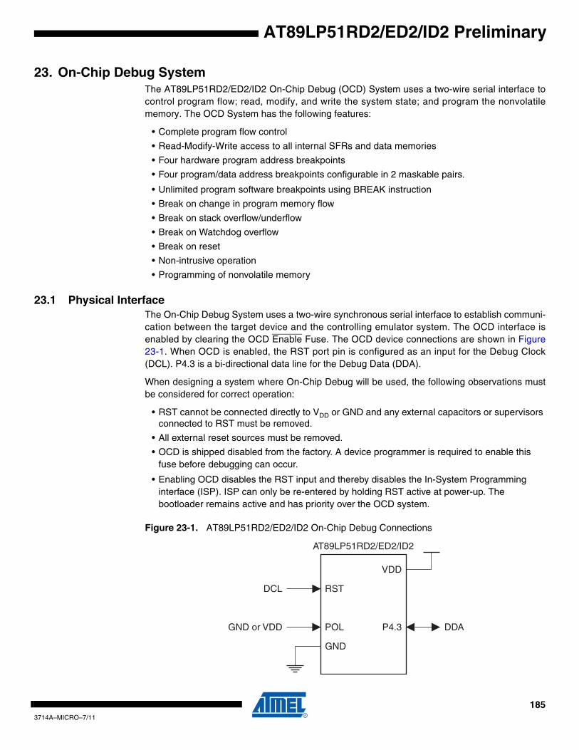
AT89LP51RD2/ED2/ID2 Preliminary
23. On-Chip Debug SystemThe AT89LP51RD2/ED2/ID2 On-Chip Debug (OCD) System uses a two-wire serial interface tocontrol program flow; read, modify, and write the system state; and program the nonvolatilememory. The OCD System has the following features:
• Complete program flow control
• Read-Modify-Write access to all internal SFRs and data memories
• Four hardware program address breakpoints
• Four program/data address breakpoints configurable in 2 maskable pairs.
• Unlimited program software breakpoints using BREAK instruction
• Break on change in program memory flow
• Break on stack overflow/underflow
• Break on Watchdog overflow
• Break on reset
• Non-intrusive operation
• Programming of nonvolatile memory
23.1 Physical InterfaceThe On-Chip Debug System uses a two-wire synchronous serial interface to establish communi-cation between the target device and the controlling emulator system. The OCD interface isenabled by clearing the OCD Enable Fuse. The OCD device connections are shown in Figure23-1. When OCD is enabled, the RST port pin is configured as an input for the Debug Clock(DCL). P4.3 is a bi-directional data line for the Debug Data (DDA).
When designing a system where On-Chip Debug will be used, the following observations mustbe considered for correct operation:
• RST cannot be connected directly to VDD or GND and any external capacitors or supervisors connected to RST must be removed.
• All external reset sources must be removed.
• OCD is shipped disabled from the factory. A device programmer is required to enable this fuse before debugging can occur.
• Enabling OCD disables the RST input and thereby disables the In-System Programming interface (ISP). ISP can only be re-entered by holding RST active at power-up. The bootloader remains active and has priority over the OCD system.
Figure 23-1. AT89LP51RD2/ED2/ID2 On-Chip Debug Connections
VDD
P4.3
RST
GND
DCL
DDA POLGND or VDD
AT89LP51RD2/ED2/ID2
1853714A–MICRO–7/11

23.2 Software BreakpointsThe AT89LP51RD2/ED2/ID2 microcontroller includes a BREAK instruction for implementingprogram memory breakpoints in software. A software breakpoint can be inserted manually byplacing the BREAK instruction in the program code. Some emulator systems may allow for auto-matic insertion/deletion of software breakpoints. The Flash memory must be re-programmedeach time a software breakpoint is changed. Frequent insertions/deletions of software break-points will reduce the endurance of the nonvolatile memory. Devices used for debuggingpurposes should not be shipped to end customers. The BREAK instruction is treated as a two-cycle NOP when OCD is disabled.
23.3 Limitations of On-Chip DebugThe AT89LP51RD2/ED2/ID2 is a fully-featured microcontroller that multiplexes several functionson its limited I/O pins. Some device functionality must be sacrificed to provide resources for On-Chip Debugging. The On-Chip Debug System has the following limitations:
• The Debug Clock pin (DCL) is physically located on the same pin as the External Reset (RST). Therefore, an external reset source is unavailable and must be emulated when OCD is enabled. The Reset Output feature is also disabled except during POR
• The Debug Data pin DDA is physically located on the same pin as P4.3. The P4.3 I/O function cannot be emulated in this mode
• The bootloader has priority over OCD. Debugging is not possible when the bootloader is active (BLJB = 0 or hardware entry triggered)
• Programming of any hardware lockbit will disable OCD
• The OCD pins are not bonded in the 40-pin PDIP package. In order to debug the device, one of the 44-pin packages must be used
1863714A–MICRO–7/11
AT89LP51RD2/ED2/ID2 Preliminary

AT89LP51RD2/ED2/ID2 Preliminary
24. Flash Memory ProgrammingThe Atmel AT89LP51RD2/ED2/ID2 microcontroller features 64K bytes of on-chip In-SystemProgrammable Flash program memory and 4K bytes of EEPROM data memory. In-System Pro-gramming allows programming and reprogramming of the microcontroller positioned inside theend system. The programmer communicates serially with the AT89LP51RD2/ED2/ID2 micro-controller, reprogramming all nonvolatile memories on the chip. In-System Programmingeliminates the need for physical removal of the chips from the system. This will save time andmoney, both during development in the lab, and when updating the software or parameters inthe field. The AT89LP51RD2/ED2/ID2 provides the following programming interfaces:
• High-Speed, four-wire SPI-based programming interface (ISP)This synchronous hardware interface programs the device while it is in reset and therefore, does not require the CPU to be operational, i.e. no clock is required except the SPI serial clock. This interface can be used both in-system and in a stand-alone programmer, and has full access to all nonvolatile memory resources. This interface is compatible with the Atmel AT89LP ISP Studio software. See Section 24.6 “In-System Programming (ISP)” on page 215 for more information.
• 12-pin parallel programming interface (PRL)This interface is a submode of the SPI interface that allows data to be read/written one 8-bit byte at a time instead of serially 1-bit at a time. This interface is intended only for stand-alone programmers. An 87C51-compatible parallel interface is not available. See Section 24.6.1 “Physical Interface” on page 215 for more information.
• ROM-based UART serial bootloader (BOOT)When using this 2-pin asynchronous interface, the device runs a default software bootloader from an on-chip ROM. The system clock must be operational and will limit the speed at which the interface functions. This interface is intended for in-system use. It has full access to the Flash code memory and EEPROM data memory, but does not have access to all configuration options. This interface is compatible with the Atmel FLIP software. See Section 24.5 “Bootloader” on page 200 for more information.
• User-defined bootloader and/or In-Application Programming (IAP)The ROM bootloader can call a user-defined bootloader located within the code memory instead of the default UART bootloader. The user is free to use any available interface to program the device. The ROM also contains an application programming interface (API) that implements the low-level routines necessary to perform in-application programming (IAP). It is recommended that users employ these functions instead of writing their own low-level routines. Advanced users may wish to implement their own routines in some cases. See Section 24.4 “In-Application Programming (IAP)” on page 192.
None of the programming interfaces require an external dedicated programming voltage. Thenecessary high programming voltage is generated on-chip using the standard VDD pin of themicrocontroller.
Note: In this document the term Bootloader, or BOOT, is used to when referring to the UART-based ROM bootloader and In-System Programming, or ISP, is used with reference to the SPI-based interface. This is different from AT89C51RD2/ED2/ID2 where ISP also referred to the bootloader (as no SPI programming interface was present). However, it should be noted that both interfaces are perfectly capable of performing in-system programming, i.e programming the device when it is already mounted in the final end-user system.
1873714A–MICRO–7/11

24.1 Memory OrganizationThe AT89LP51RD2/ED2/ID2 offers 64K bytes of In-System Programmable nonvolatile Flashcode memory and 4K bytes of nonvolatile EEPROM data memory. In addition, the device con-tains a 512-byte User Signature Array, a 128-byte read-only Atmel Signature Array and 19 UserConfiguration Fuses. The memory organization is shown in Table 24-1 and Figure 24-1. Thecode memory and auxiliary memories are divided into pages of 128 bytes each and share a tem-porary page buffer of 64 bytes (one half page). A single page erase operation will erase anentire 128-byte page, while a single write operation will only program half of a page. Therefore,two write operations are required for every erase operation when the whole page must be repro-grammed. This detail is transparent to the user when using the bootloader or Flash API.
The EEPROM data memory has a page size of 32 bytes and its own 32-byte page buffer. TheEEPROM supports erase/write operations on any number of bytes, 1–32, within a page withoutaffecting the other bytes in that page.
Figure 24-1. AT89LP51RD2/ED2/ID2 Memory Organization
.
Table 24-1. AT89LP51RD2/ED2/ID2 Memory Organization
Memory Capacity Page Size # Pages Address Range
Code Flash 65536 bytes 128 bytes 512 0000H – FFFFH
Data EEPROM 4096 bytes 32 bytes 128 0000H – 0FFFH
User Signature 512 bytes 128 bytes 4 0000H – 01FFH
Atmel Signature 128 bytes 128 bytes 1 0200H – 027FH
Page 511 Low
Page 510 Low
User Fuse Row
User Signature Array
Atmel Signature Array
Code Memory
00 3F 0000
FFFF
Page 0 0000
0FFF
Data Memory
Page 511 High
Page 510 High
40 7F
Page 128
Page 0 Low
Page 0 Low
Page 1 Low
Page 0 High
Page 1 High
Page 0 Low
Page 1 Low
Page 0 Low
Page 1 High
Page 1 High
Page 0 High
00 3F
Page Buffer
00 1F
Page 2 Low
Page 3 Low
Page 2 High
Page 3 High
SSB
BSB
SBV
OSCCAL
00 3F 40 7F
00 1F
Page Buffer
1883714A–MICRO–7/11
AT89LP51RD2/ED2/ID2 Preliminary

AT89LP51RD2/ED2/ID2 Preliminary
24.1.1 User Signature ArrayThe AT89LP51RD2/ED2/ID2 includes a 512-byte User Signature Array in four 128-byte pages.The User Signature Array is available for serial numbers, firmware revision information, datecodes or other user parameters. The User Signature Array may only be written by an externalISP programmer when the User Signature Programming Fuse is enabled. When the fuse isenabled, Chip Erase will also erase the third page of the array. When the fuse is disabled, noneof the pages are affected by page erase/write commands and only pages one and two will beerased by Chip Erase. Table 24-3 summarizes this behavior. Programming of the SignatureArray is also disabled by the Lock Bits. However, reading the signature is always allowed andthe array should not be used to store security sensitive information. The User Signature Arraymay be modified during execution through the In-Application Programming interface, regardlessof the state of the User Signature Programming fuse or Lock Bits.
Some locations of the User Signature Array have special meaning for the system as shown inTable 24-2. Pages one and two store bytes necessary for bootloader operation (See “Boot-loader” on page 200). Page three stores a calibration byte for the internal RC Oscillator. Thisbyte is read at power-up to set the frequency of the oscillator. Other bytes in these pages maybe used as additional signature space; however, care should be taken to preserve the parame-ter values when modifying other bytes in the same page.
Note: 1. The Oscillator Calibration Byte controls the frequency of the internal RC oscillator. The fre-quency is inversely proportional to the calibration value such that higher values result in lower frequencies. A copy of the factory-set calibration value is stored at location 0008H of the Atmel Signature.
Notes: 1. During ISP, a page erase/write of the user signature is only allowed when the User SIgnature Programming Fuse is active.
2. Chip Erase will erase this page only if the User SIgnature Programming Fuse is active.
Table 24-2. User Signature Parameter Bytes
Name Definition Location Default Value
BSB Boot Status Byte 0000H FFH
SBV Software Boot Vector 0001H FCH (or FFH)
SSB Software Security Byte 0080H FFH
OSCCAL Oscillator Calibration 0180H (1)
Table 24-3. User Signature ISP Programming Behavior
Page # Address Chip Erase Page Erase Page Write
0 0000–007FH YES By Fuse(1) By Fuse(1)
1 0080–00HFH YES By Fuse(1) By Fuse(1)
2 0100–017FH By Fuse(2) By Fuse(1) By Fuse(1)
3 0180–01FFH NO By Fuse(1) By Fuse(1)
1893714A–MICRO–7/11

24.1.2 Atmel Signature ArrayThe Atmel Signature Array is a 128-byte read-only array that contains the Device ID and relatedinformation. The Device ID values are shown in Table 24-4. A copy of the OSCCAL calibrationbyte is also stored at address 0008H.
24.2 User Configuration FusesThe AT89LP51RD2/ED2/ID2 includes 19 user fuses for configuration of the device. Each fuse isaccessed at a separate address in the User Fuse Row, with each byte representing one fuse aslisted in Table 24-5. From a programming standpoint, fuses are treated the same as normalcode bytes except they are not affected by Chip Erase. Fuses can be cleared at any time by writ-ing 00H to the appropriate locations in the fuse row. However, to set a fuse, i.e. write it to FFHthe entire fuse row must be erased and then reprogrammed. The programmer should read thestate of all the fuses into a temporary location, modify those fuses which need to be disabled,then issue a Fuse Write with Auto-Erase command using the temporary data.
Note that the bootloader only has limited access to the fuses. For full device configuration anexternal ISP programmer is required.
Table 24-4. Device ID Values in Atmel Signature
Device 00H 01H 02H 30H 31H 60H 61H
AT89LP51RD2 1EH 64H 72H 58H D7H ECH EFH
AT89LP51ED2 1EH 64H 65H 58H D7H ECH EFH
AT89LP51ID2 1EH 64H 69H 58H D7H ECH EFH
Table 24-5. User Configuration Fuse Definitions
Address Fuse Name Description
00 – 01H Clock Source A – CSA[0:1](2)
Selects source for the system clock when using OSCA:
CSA1 CSA0 Selected Source
FFh FFh High Speed Crystal Oscillator on XTAL1A/XTAL2A (XTAL)
FFh 00h Low Power Crystal Oscillator on XTAL1A/XTAL2A (XTAL)
00h FFh External Clock on XTAL1A (XCLK)
00h 00h Internal 8 MHz RC Oscillator (IRC)
02 – 03H Start-up Time – SUT[0:1]
Selects time-out delay for the POR/BOD/PWD wake-up period:
SUT1 SUT0 Selected Time-out
00h 00h 1 ms (XTAL); 16 µs (XCLK/IRC)
00h FFh 2 ms (XTAL); 512 µs (XCLK/IRC)
FFh 00h 4 ms (XTAL); 1 ms (XCLK/IRC)
FFh FFh 16 ms (XTAL); 4 ms (XCLK/IRC)
04H Bootloader Jump BitFFh: Reset to user application at 0000H00h: Reset to ROM bootloader at F800H
05H External RAM EnableFFh: External RAM enabled at reset (EXTRAM = 1)00h: External RAM disabled at reset (EXTRAM = 0)
06H Compatibility ModeFFh: CPU functions in 12-clock Compatibility mode00h: CPU functions is single-cycle Fast mode
07H ISP Enable(3) FFh: In-System Programming Enabled00h: In-System Programming Disabled (Enabled at POR only)
1903714A–MICRO–7/11
AT89LP51RD2/ED2/ID2 Preliminary

AT89LP51RD2/ED2/ID2 Preliminary
Notes: 1. The default state from the factory for all fuses is FFh, except for the Tristate Ports and Bootloader Jump Bit, which are 00H.
2. Changes to these fuses will only take effect after a device POR.
3. Changes to these fuses will only take effect after the ISP session terminates by bringing RST inactive.
24.3 Flash Hardware SecurityThe AT89LP51RD2/ED2/ID2 provides three Hardware Security Bits (or Lock Bits) for FlashCode Memory and Data EEPROM security. Security bits can be left unprogrammed (FFh) orprogrammed (00h) to obtain the protection levels listed in Table 24-6. Security bits can only beerased (set to FFh) by Chip Erase. Lock bit mode 2 disables programming of all memoryspaces, including the User Signature Array and User Configuration Fuses. User fuses must beprogrammed before enabling Lock bit mode 2 or 3. Lock bit mode 3 implements mode 2 andalso blocks reads from the code and data memories; however, reads of the User SignatureArray, Atmel Signature Array, and User Configuration Fuses are still allowed.
The Hardware Security bits only restrict the access of the SPI-based ISP interface. The Hard-ware Security Bits will not disable the Bootloader or any programming initiated by the applicationsoftware using IAP.
08H X1/X2 ModeFFh: X1 Mode (System clock is divided-by-two)00h: X2 Mode (System clock is not divided-by-two)
09H OCD EnableFFh: On-Chip Debug is Disabled00h: On-Chip Debug is Enabled
0AH User Signature ProgrammingFFh: Programming of User Signature Disabled00h: Programming of User Signature Enabled
0BH Tristate PortsFFh: I/O Ports start in input-only mode (tristated) after reset00h: I/O Ports start in quasi-bidirectional mode after reset
0CH EEPROM EraseFFh: EEPROM is erased during chiperase00h: EEPROM is not erased during chiperase
0D – 0EH Low Power Mode – LPM[0:1]
Selects source for the system clock when using OSCA:
LPM1 LPM0 Power Mode
FFh FFh Low Power Mode
FFh 00h Normal Mode
00h FFh Extra Low Power Mode (FOSC ≤ 1 MHz)
00h 00h Normal Mode
0FH R1 EnableFFh: 5 MΩ resistor on XTAL1A Disabled00h: 5 MΩ resistor on XTAL1A Enabled
10H Oscillator Select00h: Boot from Oscillator B (AT89LP51ID2 Only)FFh: Boot from Oscillator A
11 – 12h Clock Source B – CSB[0:1](2)
Selects source for the system clock when using OSCB (AT89LP51ID2 Only):
CSB1 CSB0 Selected Source
FFh FFh Low Frequency Crystal Oscillator on XTAL1B/XTAL2B (XTAL)
FFh 00h Low Frequency Crystal Oscillator on XTAL1B/XTAL2B (XTAL)
00h FFh External Clock on XTAL1B (XCLK)
00h 00h Internal 8 MHz RC Oscillator (IRC)
Table 24-5. User Configuration Fuse Definitions
Address Fuse Name Description
1913714A–MICRO–7/11

24.4 In-Application Programming (IAP)The AT89LP51RD2/ED2/ID2 supports In-Application Programming (IAP), allowing the programmemory to be modified during execution. IAP can be used to modify the user application on thefly or to use program memory for nonvolatile data storage. The AT89LP51RD2/ED2/ID2includes a Flash Application Programming Interface (API) as part of the bootloader ROM code.The Flash API is the preferred way to program the Flash memory from the application code.Advanced users looking to write their own low-level routines should refer to Section 24.4.2 onpage 194.
24.4.1 API Call DescriptionThe In-Application Programming (IAP) feature allows reprogramming a microcontroller on-chipFlash memory without removing it from the system and while the embedded application is run-ning. The user application can call Flash Application Programming Interface (API) routinesallowing IAP. These Flash API are also executed by the bootloader.
To call the corresponding API, the user may use a set of routines which can be linked with theapplication. Example of Flash_api routines are available on the Atmel web site on the softwareapplication note:
C Flash Drivers for the AT89C51RD2/ED2
The API calls description and arguments are shown in Table 24-7.
The application selects an API by setting R1, ACC, DPTR0 and DPTR1 registers. All calls aremade through a common interface “USER_CALL” at the address FFF0h. The jump to theUSER_CALL must be done by an LCALL instruction in order to be able to return to the applica-tion. Before jumping to USER_CALL, the bit ENBOOT in AUXR1 register must be set to map theROM code into the address space.
Flash API calls have the following constraints:
• The interrupts are not disabled by the bootloader. Interrupts must be disabled by the user prior to calling USER_CALL, then re-enabled when returning.
• The user must feed the hardware watchdog before launching a Flash operation.
• The API call requires a minimum of two free stack bytes
Table 24-6. Security Protection Modes
Program Lock Bits (by address)
Mode 00h 01h 02h Protection Mode
1 FFh FFh FFh No program lock features
2 00h FFh FFh Further programming of the Flash is disabled
3 00h 00h FFh Further programming of the Flash is disabled and verify (read) is also disabled
4 00h 00h 00hFurther programming of the Flash is disabled and verify (read) is also disabled; External execution above 32K when BMS = 1 is disabled
1923714A–MICRO–7/11
AT89LP51RD2/ED2/ID2 Preliminary
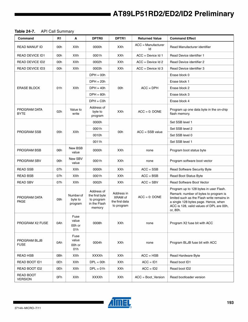
AT89LP51RD2/ED2/ID2 Preliminary
Table 24-7. API Call Summary
Command R1 A DPTR0 DPTR1 Returned Value Command Effect
READ MANUF ID 00h XXh 0000h XXhACC = Manufacturer
IdRead Manufacturer identifier
READ DEVICE ID1 00h XXh 0001h XXh ACC = Device Id 1 Read Device identifier 1
READ DEVICE ID2 00h XXh 0002h XXh ACC = Device Id 2 Read Device identifier 2
READ DEVICE ID3 00h XXh 0003h XXh ACC = Device Id 3 Read Device identifier 3
ERASE BLOCK 01h XXh
DPH = 00h
00h ACC = DPH
Erase block 0
DPH = 20h Erase block 1
DPH = 40h Erase block 2
DPH = 80h Erase block 3
DPH = C0h Erase block 4
PROGRAM DATA BYTE
02hValue to
write
Address of byte to
programXXh ACC = 0: DONE
Program up one data byte in the on-chip flash memory.
PROGRAM SSB 05h XXh
0000h
00h ACC = SSB value
Set SSB level 1
0001h Set SSB level 2
0010h Set SSB level 0
0011h Set SSB level 1
PROGRAM BSB 06hNew BSB
value0000h XXh none Program boot status byte
PROGRAM SBV 06hNew SBV
value0001h XXh none Program software boot vector
READ SSB 07h XXh 0000h XXh ACC = SSB Read Software Security Byte
READ BSB 07h XXh 0001h XXh ACC = BSB Read Boot Status Byte
READ SBV 07h XXh 0002h XXh ACC = SBV Read Software Boot Vector
PROGRAM DATA PAGE
09hNumber of
byte to program
Address of the first byte to program in the Flash
memory
Address in XRAM of
the first data to program
ACC = 0: DONE
Program up to 128 bytes in user Flash.
Remark: number of bytes to program is limited such as the Flash write remains in a single 128 bytes page. Hence, when ACC is 128, valid values of DPL are 00h, or, 80h.
PROGRAM X2 FUSE 0Ah
Fuse value
00h or 01h
0008h XXh none Program X2 fuse bit with ACC
PROGRAM BLJB FUSE
0Ah
Fuse value
00h or 01h
0004h XXh none Program BLJB fuse bit with ACC
READ HSB 0Bh XXh XXXXh XXh ACC = HSB Read Hardware Byte
READ BOOT ID1 0Eh XXh DPL = 00h XXh ACC = ID1 Read boot ID1
READ BOOT ID2 0Eh XXh DPL = 01h XXh ACC = ID2 Read boot ID2
READ BOOT VERSION
0Fh XXh XXXXh XXh ACC = Boot_Version Read bootloader version
1933714A–MICRO–7/11

24.4.2 Low-Level InterfaceThe CPU interfaces to the Flash memory through the FCON register (Table 24-10) and EECONregister (Table 3-5 on page 25). These registers are used to:
• Map the memory spaces in the addressable space
• Launch the programming of the memory spaces
• Get the status of the Flash memory (busy/not busy)
CAUTION: The incorrect usage of these functions can make the system unstable or inoperable.
For internal execution from user space the AT89LP51RD2/ED2/ID2 uses an idle-while-writearchitecture where the CPU is placed in an idle state while programming occurs. When the writecompletes, the CPU will continue executing with the instruction after the instruction that startedthe write sequence (usually a MOV to FCON). All peripherals will continue to function during thewrite cycle; however, interrupts will not be serviced until the write completes.
For external execution from user space the AT89LP51RD2/ED2/ID2 uses an execute-while-write architecture where the CPU continues to operate while the programming occurs. The soft-ware should poll the state of the FBUSY flag to determine when the write completes. Interruptsmust be disabled during the write sequence as the CPU will not be able to vector to the internalinterrupt table and care should be taken that the application does not jump to an internal addressuntil the programming completes.
The Flash API routines in the Boot ROM also use execute-while-write. Interrupts must be dis-abled before calling the routines to prevent the CPU from vectoring to a non-ROM addressbefore the programming completes.
Flash memory uses a page-based programming model. Flash data memory differs from tradi-tional EEPROM data memory in the method of writing data. EEPROM generally can update asingle byte with any value. Flash memory splits programming into write and erase operations. AFlash write can only program zeroes, i.e change ones into zeroes ( ). Any ones in the writedata are ignored. A Flash erase sets an entire page of data to ones so that all bytes becomeFFH. Therefore after an erase, each byte in the page can only be written once with any possiblevalue. Bytes can be overwritten without an erase as long as only ones are changed into zeroes.However, if even a single bit needs updating from zero to one ( ); then the contents of thepage must first be saved, the entire page must be erased and the zero bits in all bytes (old andnew data combined) must be written. Avoiding unnecessary page erases greatly improves theendurance of the memory.
24.4.2.1 Mapping of the Memory SpaceBy default, the user application space of the Flash Code memory is accessed read-only by theMOVC instruction. The Flash temporary page buffer is made accessible (write-only) by settingthe FPS bit in FCON register. Writing is possible from 0000H to FFFFF, address bits 6 to 0 areused to select an address within a page while bits 15 to 7 are used to select the programmingaddress of the page. Setting FPS takes precedence over the EXTRAM bit in AUXR.
The other memory spaces (User and Atmel Signatures, User Fuses, Hardware Security) aremade accessible in the code segment by programming bits FMOD0 and FMOD1 in FCON regis-ter in accordance with Table 24-8. A MOVC instruction can then be used for reading thesespaces.
1 0→
0 1→
1943714A–MICRO–7/11
AT89LP51RD2/ED2/ID2 Preliminary

AT89LP51RD2/ED2/ID2 Preliminary
24.4.2.2 Launching ProgrammingThe FPL bits in the FCON register are used to secure the launch of programming. A specificsequence must be written in these bits to unlock the write protection and to launch the program-ming. This sequence is 5xH followed by AxH. Table 24-9 summarizes the programming of thememory spaces according to the FMOD bits.
Notes: 1. The sequence 5xH and AxH must be executing without instructions between them otherwise the programming is aborted.
2. Interrupts that may occur during programming time must be disabled to avoid any spurious exit of the programming mode.
24.4.2.3 Status of the Flash MemoryThe bit FBUSY in FCON register is used to indicate the status of programming. FBUSY is setwhen programming is in progress and cleared when the programming completes. If program-ming was interrupted due to a brown-out condition the ERR flag in EECON is set.
24.4.2.4 Loading the Page BufferThe AT89LP51RD2/ED2/ID2 includes a temporary page buffer of 64 bytes, or one half of apage. Because the page buffer is 64 bytes long, the maximum number of bytes written at onetime is 64. Therefore, two write cycles are required to fill an entire 128-byte page, one for the lowhalf page (00H–3FH) and one for the high half page (40H–7FH) as shown in Figure 24-2.
Table 24-8. Memory Selection
FMOD1 FMOD0 Addressable space
0 0 User Application (0000–FFFFH)
0 1User Signature (0000–01FFH)
Atmel Signature (0200–027FH read-only)
1 0User Fuses (0000–007FH)
Hardware Security Bits (0080–00FFH read-only)
1 1 Reserved
Table 24-9. Programming Sequences
Memory
Write to FCON
OperationFPL3-0 FPS FMOD1 FMOD0
User Application(CODE)
5 X 0 0 No action
A X 0 0Write the page buffer to user space (0000–FFFFH)
User Signature
5 X 0 1 No action
A X 0 1Write the page buffer to User Signature space (0000–01FFH)
User Fuses
5 X 1 0 No action
A X 1 0Write the page buffer to User Fuse space (0000–007FH)
Reserved5 X 1 1 No action
A X 1 1 No action
1953714A–MICRO–7/11

Figure 24-2. Page Programming Structure
Any number of data bytes from 1 to 64 can be loaded into the temporary page buffer. This pro-vides the capability to program the whole memory by byte, by half-page or by any number ofbytes in a half-page. Note that once loaded, a buffer location cannot be reloaded with anothervalue. The page buffer is automatically cleared after each erase/write operation.
By default no erase is performed prior to writing the page buffer contents to the Flash array. Anyunloaded locations remain unchanged. Any zeroes in the loaded locations will be written to thedesired page. The auto-erase bit AERS (EECON.6) can be set to one to perform a page eraseautomatically at the beginning of any write sequence. The page erase will erase the entire page,i.e. both the low and high half pages. However, the write operation paired with the auto-erasecan only program one of the half pages. A second write cycle without auto-erase is required toupdate the other half page. When AERS = 1 any unloaded locations will be left blank (FFH) afterthe operation completes.
The following procedure is used to load the page buffer and is summarized in Figure 24-3:
1. Save then disable interrupts (EA = 0)
2. Map the page buffer space by setting FPS = 1
3. Load the DPTR (or /DPTR) with the address to load
4. Load Accumulator register with the data to load
5. Execute the MOVX @DPTR, A instruction (or MOVX @/DPTR, A instruction)
6. If needed loop the steps 3—5 until the page buffer is completely loaded
7. Unmap the page buffer (FPS = 0) and restore interrupts (EA = 1)
24.4.2.5 Programming the Flash Code SpaceThe following procedure is used to program the User code space and is summarized in Figure24-4:
1. Load up to one half-page of data in the page buffer from address 0000H to FFFFH
2. Save then disable the interrupts (EA = 0)
3. Launch the programming by writing the data sequence 50H followed by A0H to FCON register
4. If launched from internal memory, the CPU idles until programming completes. If launched from external memory, poll the FBUSY flag until it is cleared
5. Restore the interrupts (EA = 1)
Low Half Page
00 3F
Data Memory High Half Page
40 7F
00 3F
Page Buffer
1963714A–MICRO–7/11
AT89LP51RD2/ED2/ID2 Preliminary

AT89LP51RD2/ED2/ID2 Preliminary
Figure 24-3. Flash Page Buffer Loading Procedure
Note: The last page address used when loading the page buffer is the one used to select the page pro-gramming address.
24.4.2.6 Programming the User Signature SpaceThe following procedure is used to program the User Signature space and is summarized in Fig-ure 24-4:
1. Load up to one half-page of data in the page buffer from address 0000H to 01FFH
2. Save then disable the interrupts (EA = 0)
3. Launch the programming by writing the data sequence 52H followed by A2H to FCON register.
4. If launched from internal memory, the CPU idles until programming completes. If launched from external memory, poll the FBUSY flag until it is cleared
5. Restore the interrupts (EA = 1)
Flash Page Buffer Loading
Data LoadDPTR = Address
ACC = DataExec: MOVX @DPTR, A
Last Byteto load?
Page Buffer MappingFCON = 08h (FPS=1)
Data memory MappingFCON = 00h (FPS = 0)
Save and Disable ITEA = 0
Restore IT
1973714A–MICRO–7/11

Figure 24-4. Flash Programming Procedure
24.4.2.7 Programming the User Fuse SpaceThe following procedure is used to program the User Fuse space and is summarized in Figure24-4:
1. Load up to one half-page of data in the page buffer from address 0000H to 01FFH
2. Save then disable the interrupts (EA = 0)
3. Launch the programming by writing the data sequence 54H followed by A4H to FCON register.
4. If launched from internal memory, the CPU idles until programming completes. If launched from external memory, poll the FBUSY flag until it is cleared
5. Restore the interrupts (EA = 1)
24.4.2.8 Reading the Flash Code SpaceThe following procedure is used to read the User code space:
1. Map the code space by writing 00H to FCON (the default)
2. Read one byte in Accumulator by executing MOVC A,@A+DPTR where A+DPTR is the address of the code byte to read
Flash Spaces Programming
Save and Disable ITEA = 0
Launch ProgrammingFCON = 5xhFCON = Axh
End ProgrammingRestore IT
Page Buffer Loadingsee Figure 24-3
FBusyCleared?
Clear ModeFCON = 00h
1983714A–MICRO–7/11
AT89LP51RD2/ED2/ID2 Preliminary

AT89LP51RD2/ED2/ID2 Preliminary
24.4.2.9 Reading the User/Atmel SignatureThe following procedure is used to read the User or Atmel Signature space and is summarizedin Figure 24-5:
• Map the Signature space by writing 02H to FCON register
• Read one byte in Accumulator by executing MOVC A,@A+DPTR where A+DPTR is 0000–01FFH for the User Signature and 0200–027FH for the Atmel Signature
• Clear FCON to unmap the Signature space
24.4.2.10 Reading the User Fuses/Hardware Security BitsThe following procedure is used to read the User Fuses or Hardware Security space andis summarized in Figure 24-5:
• Map the User Fuses/Hardware Security space by writing 04H in FCON register
• Read one byte in Accumulator by executing MOVC A,@A+DPTR where A+DPTR is 0000–007FH for the User Fuses and 0080–00FFH for the Hardware Security
• Clear FCON to unmap the User Fuses/Hardware Security
Figure 24-5. Reading Procedure
Note: aa = 00B for the User Application Codeaa = 01B for the User/Atmel Signatureaa = 10B for the User Fuses/Hardware Security
Flash Spaces Reading
Flash Spaces MappingFCON = 00000aa0
Data ReadDPTR = Address
ACC = 0Exec: MOVC A, @A+DPTR
Clear ModeFCON = 00h
1993714A–MICRO–7/11
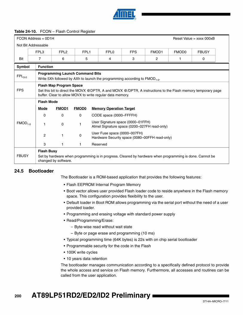
24.5 BootloaderThe Bootloader is a ROM-based application that provides the following features:
• Flash EEPROM Internal Program Memory
• Boot vector allows user provided Flash loader code to reside anywhere in the Flash memory space. This configuration provides flexibility to the user.
• Default loader in Boot ROM allows programming via the serial port without the need of a user provided loader.
• Programming and erasing voltage with standard power supply
• Read/Programming/Erase:
– Byte-wise read without wait state
– Byte or page erase and programming (10 ms)
• Typical programming time (64K bytes) is 22s with on chip serial bootloader
• Programmable security for the code in the Flash
• 100K write cycles
• 10 years data retention
The bootloader manages communication according to a specifically defined protocol to providethe whole access and service on Flash memory. Furthermore, all accesses and routines can becalled from the user application.
Table 24-10. FCON – Flash Control Register
FCON Address = 0D1H Reset Value = xxxx 000xB
Not Bit Addressable
FPL3 FPL2 FPL1 FPL0 FPS FMOD1 FMOD0 FBUSY
Bit 7 6 5 4 3 2 1 0
Symbol Function
FPL3-0Programming Launch Command BitsWrite 5Xh followed by AXh to launch the programming according to FMOD1-0.
FPSFlash Map Program SpaceSet this bit to direct the MOVX @DPTR, A and MOVX @/DPTR, A instructions to the Flash memory temporary page buffer. Clear to allow MOVX to write regular data memory.
FMOD1-0
Flash Mode
Mode FMOD1 FMOD0 Memory Operation Target
0 0 0 CODE space (0000–FFFFH)
1 0 1User Signature space (0000–01FFH)Atmel Signature space (0200–027FH read-only)
2 1 0User Fuse space (0000–007FH)Hardware Security space (0080–00FFH read-only)
3 1 1 Reserved
FBUSYFlash BusySet by hardware when programming is in progress. Cleared by hardware when programming is done. Cannot be changed by software.
2003714A–MICRO–7/11
AT89LP51RD2/ED2/ID2 Preliminary

AT89LP51RD2/ED2/ID2 Preliminary
Figure 24-6. Diagram Context Description
Table 24-11 list some acronyms used by the Bootloader.
On Figure 24-7, the on-chip bootloader processes are:
• ISP Communication ManagementThe purpose of this process is to manage the communication and its protocol between the on-chip bootloader and a external device. The on-chip ROM implements a serial protocol (see section “Bootloader Protocol Description” on page 206). This process translate serial communication frame (UART) into Flash memory access (read, write, erase, etc.).
• User Call ManagementSeveral Application Program Interface (API) calls are available for use by an application program to permit selective erasing and programming of Flash pages. All calls are made through a common interface (API calls), included in the ROM bootloader. The programming functions are selected by setting up the microcontroller’s registers before making a call to a common entry point (0xFFF0). Results are returned in the registers. The purpose on this process is to translate the registers values into internal Flash Memory Management. See “In-Application Programming (IAP)” on page 192
• Flash Memory ManagementThis process manages low level access to Flash memory (performs read and write access).
Bootloader Flash Memory
Access ViaSpecificProtocol
Access FromUserApplication
Table 24-11. Bootload Definitions
Mnemonic Definition
BSB Boot Status Byte
HW/HSB Hardware Byte/Hardware Security Byte
SBV Software Boot Vector
SSB Software Security Byte
2013714A–MICRO–7/11
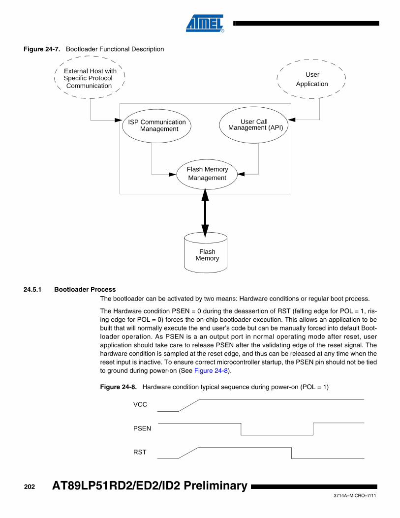
Figure 24-7. Bootloader Functional Description
24.5.1 Bootloader ProcessThe bootloader can be activated by two means: Hardware conditions or regular boot process.
The Hardware condition PSEN = 0 during the deassertion of RST (falling edge for POL = 1, ris-ing edge for POL = 0) forces the on-chip bootloader execution. This allows an application to bebuilt that will normally execute the end user’s code but can be manually forced into default Boot-loader operation. As PSEN is a an output port in normal operating mode after reset, userapplication should take care to release PSEN after the validating edge of the reset signal. Thehardware condition is sampled at the reset edge, and thus can be released at any time when thereset input is inactive. To ensure correct microcontroller startup, the PSEN pin should not be tiedto ground during power-on (See Figure 24-8).
Figure 24-8. Hardware condition typical sequence during power-on (POL = 1)
ISP CommunicationManagement
UserApplication
Specific ProtocolCommunication
Management
FlashMemory
External Host with
Flash Memory
User CallManagement (API)
VCC
PSEN
RST
2023714A–MICRO–7/11
AT89LP51RD2/ED2/ID2 Preliminary

AT89LP51RD2/ED2/ID2 Preliminary
The on-chip bootloader boot process is shown Figure 24-9 on page 204 and described in Table .
24.5.2 Bootloader ResourcesSeveral on-chip resources are provided for use by the bootloader.
24.5.2.1 Hardware RegisterThe hardware register of the AT89LP51RD2/ED2/ID2 is called the Hardware Byte or HardwareSecurity Byte (HSB). It is a shadow of selected resources from the User Fuses and HardwareSecurity Bits.
Table 24-12. Hardware Security Byte (HSB)
Bootloader Process Description
Purpose
Hardware ConditionThe Hardware Condition forces the bootloader execution whatever the BLJB, BSB and SBV values.
BLJB
The Boot Loader Jump Bit forces the application execution.BLJB = 0 => Bootloader executionBLJB = 1 => Application execution
The BLJB is a User configuration fuse. It can be modified by hardware (programmer) or by software (API). Note: The BLJB test is performed by hardware to prevent any program execution.
SBV
The Software Boot Vector contains the high address of customer bootloader stored in the application.SBV = FCh (default value) if no customer bootloader in user Flash.
Note: The customer bootloader is called by JMP [SBV]00h instruction.
7 6 5 4 3 2 1 0
X2 BLJB - - XRAM LB2 LB1 LB0
Bit Number
Bit Mnemonic Description
7 X2X2 ModeProgrammed (‘0’ value) to force X2 mode after reset.
Unprogrammed (‘1’ Value) to force X1 mode after reset (Default).
6 BLJB
Boot Loader Jump Bit
Unprogrammed (‘1’ value) to start the user’s application on next reset at address 0000h.
Programmed (‘0’ value) to start the boot loader at address F800h on next reset (Default).
5 OSC
Oscillator Bit
Programmed to allow oscillator B at startup
Unprogrammed this bit to allow oscillator A at startup (Default).
4 - Reserved
3 XRAM
XRAM config bit (only programmable by programmer tools)
Programmed to inhibit XRAM.
Unprogrammed, this bit to valid XRAM (Default).
2-0 LB2-0User Memory Lock Bits (only programmable by programmer tools)
See Table 24-13
2033714A–MICRO–7/11
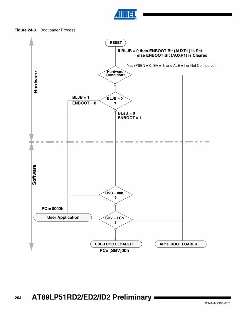
Figure 24-9. Bootloader Process
RESET
HardwareCondition?
BLJB!= 0?
User Application
Har
dw
are
So
ftw
are
Atmel BOOT LOADERUSER BOOT LOADER
BLJB = 1
BSB = 00h?
SBV = FCh?
PC = 0000h
PC= [SBV]00h
BLJB = 0
If BLJB = 0 then ENBOOT Bit (AUXR1) is Setelse ENBOOT Bit (AUXR1) is Cleared
ENBOOT = 1
ENBOOT = 0
Yes (PSEN = 0, EA = 1, and ALE =1 or Not Connected)
2043714A–MICRO–7/11
AT89LP51RD2/ED2/ID2 Preliminary
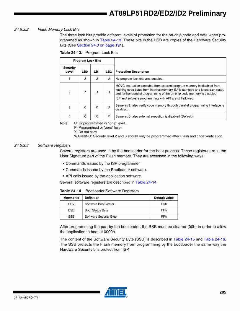
AT89LP51RD2/ED2/ID2 Preliminary
24.5.2.2 Flash Memory Lock BitsThe three lock bits provide different levels of protection for the on-chip code and data when pro-grammed as shown in Table 24-13. These bits in the HSB are copies of the Hardware SecurityBits (See Section 24.3 on page 191).
Table 24-13. Program Lock Bits
Note: U: Unprogrammed or "one" level. P: Programmed or "zero" level. X: Do not careWARNING: Security level 2 and 3 should only be programmed after Flash and code verification.
24.5.2.3 Software RegistersSeveral registers are used in by the bootloader for the boot process. These registers are in theUser Signature part of the Flash memory. They are accessed in the following ways:
• Commands issued by the ISP programmer
• Commands issued by the Bootloader software.
• API calls issued by the application software.
Several software registers are described in Table 24-14.
After programming the part by the bootloader, the BSB must be cleared (00h) in order to allowthe application to boot at 0000h.
The content of the Software Security Byte (SSB) is described in Table 24-15 and Table 24-16.The SSB protects the Flash memory from programming by the bootloader the same way theHardware Security bits protect from ISP.
Program Lock Bits
Protection DescriptionSecurity
Level LB0 LB1 LB2
1 U U U No program lock features enabled.
2 P U U
MOVC instruction executed from external program memory is disabled from fetching code bytes from internal memory, EA is sampled and latched on reset, and further parallel programming of the on chip code memory is disabled.
ISP and software programming with API are still allowed.
3 X P USame as 2, also verify code memory through parallel programming interface is disabled.
4 X X P Same as 3, also external execution is disabled (Default).
Table 24-14. Bootloader Software Registers
Mnemonic Definition Default value
SBV Software Boot Vector FCh
BSB Boot Status Byte FFh
SSB Software Security Byte FFh
2053714A–MICRO–7/11

Table 24-15. Software Security Byte
The two lock bits provide different levels of protection for the on-chip code and data, when pro-grammed as shown in Table 24-16.
Table 24-16. User Memory Lock Bits of the SSB
Note: X: Do not careWARNING: Security level 2 and 3 should only be programmed after Flash verification.
24.5.3 Bootloader Protocol Description
24.5.3.1 Physical LayerThe UART used to transmit information has the following configuration:
• Character: 8-bit data
• Parity: none
• Stop: 2 bits
• Flow control: none
• Baud Rate: autobaud is performed by the bootloader to compute the baud rate chosen by the host.
7 6 5 4 3 2 1 0
- - - - - - LB1 LB0
Bit
Number
Bit
Mnemonic Description
7 -ReservedDo not clear this bit.
6 -ReservedDo not clear this bit.
5 -ReservedDo not clear this bit.
4 -ReservedDo not clear this bit.
3 -ReservedDo not clear this bit.
2 -ReservedDo not clear this bit.
1-0 LB1-0User Memory Lock Bits
See Table 24-16
Program Lock Bits
Protection DescriptionSecurity
Level LB0 LB1
1 1 1 No program lock features enabled.
2 0 1 Bootloader programming of the Flash is disabled.
3 X 0 Same as 2, also verify through Bootloader programming interface is disabled.
2063714A–MICRO–7/11
AT89LP51RD2/ED2/ID2 Preliminary

AT89LP51RD2/ED2/ID2 Preliminary
24.5.3.2 Frame DescriptionThe Serial Protocol is based on the Intel Hex-type records.
Intel Hex records consist of ASCII characters used to represent hexadecimal values and aresummarized below.
Figure 24-10. Intel Hex Type Frame
• Record Mark:Record Mark is the start of frame. This field must contain ’:’.
• Reclen:Reclen specifies the number of bytes of information or data which follows the Record Type field of the record.
• Load Offset:Load Offset specifies the 16-bit starting load offset of the data bytes, therefore this field is used only for Data Program Record (see Section “Bootloader Command Summary”).
• Record Type:Record Type specifies the command type. This field is used to interpret the remaining information within the frame. The encoding for all the current record types is described in Section “Bootloader Command Summary”.
• Data/Info:Data/Info is a variable length field. It consists of zero or more bytes encoded as pairs of hexadecimal digits. The meaning of data depends on the Record Type.
• Checksum:The two’s complement of the 8-bit bytes that result from converting each pair of ASCII hexadecimal digits to one byte of binary, and including the Reclen field to and including the last byte of the Data/Info field. Therefore, the sum of all the ASCII pairs in a record after converting to binary, from the Reclen field to and including the Checksum field, is zero.
24.5.4 Functional Description
24.5.4.1 Software Security Bits (SSB)The SSB protects any Flash access from Bootloader commands. The command "Program Soft-ware Security Bit" can only write a higher priority level. There are three levels of security:
• level 0: NO_SECURITY (FFh)This is the default level.From level 0, one can write level 1 or level 2.
• level 1: WRITE_SECURITY (FEh)For this level it is impossible to write in the Flash memory, BSB or SBV. The Bootloader returns ’P’ on write access. From level 1, one can write only level 2.
• level 2: RD_WR_SECURITY (FCh)Level 2 forbids all read and write accesses to/from the Flash/EEPROM memory. The Bootloader returns ’L’ on read or write access. Only a full chip erase in parallel mode (using a programmer) or ISP command can reset the software security bits. From level 2, one cannot read and write anything.
Record Record Load Data
Mark’:’
Reclen Offset Typeor
InfoChecksum
1-byte 1-byte 2-bytes 1-byte n-bytes 1-byte
2073714A–MICRO–7/11

24.5.4.2 Full Chip EraseThe ISP command "Full Chip Erase" erases all user Flash memory (fills with FFh) and setssome bytes used by the bootloader at their default values:
• BSB = FFh
• SBV = FCh
• SSB = FFh
The Full Chip Erase does not affect the bootloader or the EEPROM.
24.5.4.3 Checksum ErrorWhen a checksum error is detected, ‘X’ is sent followed with CR&LF.
24.5.5 Flow Description
24.5.5.1 OverviewAn initialization step must be performed after each Reset. After microcontroller reset, the boot-loader waits for an autobaud sequence (see section “Autobaud Performance” ). After thecommunication is initialized, the protocol depends on the record type requested by the host.FLIP, a software utility to implement bootloader programming with a PC, is available from theAtmel web site.
24.5.5.2 Communication InitializationThe host initializes the communication by sending a ’U’ character to help the bootloader to com-pute the baud rate (autobaud).
Figure 24-11. Initialization
Table 24-17. Software Security Byte Behavior
Level 0 Level 1 Level 2
Flash/EEPROM Any access allowed Read-only access allowed Any access not allowed
Fuse Bit Any access allowed Read-only access allowed Any access not allowed
BSB & SBV Any access allowed Read-only access allowed Any access not allowed
SSB Any access allowed Write level 2 allowed Read-only access allowed
Manufacturer Info Read-only access allowed Read-only access allowed Read-only access allowed
Bootloader Info Read-only access allowed Read-only access allowed Read-only access allowed
Erase Block Allowed Not allowed Not allowed
Full Chip Erase Allowed Allowed Allowed
Blank Check Allowed Allowed Allowed
Host Bootloader
"U"Performs Autobaud
Init Communication
If (Not Received "U") "U"
Communication OpenedElse
Sends Back “U” Characte
2083714A–MICRO–7/11
AT89LP51RD2/ED2/ID2 Preliminary

AT89LP51RD2/ED2/ID2 Preliminary
24.5.5.3 Autobaud PerformanceThe bootloader feature allows a wide range of baud rates in the user application. It is also adapt-able to a wide range of oscillator frequencies. This is accomplished by measuring the bit-time ofa single bit in a received character. This information is then used to program the baud rate interms of timer counts based on the oscillator frequency. The bootloader feature requires that aninitial character (an uppercase U) be sent to the AT89LP51RD2/ED2/ID2 to establish the baudrate. Table 24-18 shows the autobaud capability.
For AT89LP51ID2 the bootloader always uses OSCA. If the device boots on OSCB, the boot-loader will enable and switch to OSCA. In this case both the OSCA and OSCB sources must beoperational, i.e. a crystal or external clock source must be connected to the oscillator inputsunless the oscillator source was previously configured as the internal RC oscillator.
Table 24-18. Autobaud Performance
Frequency (MHz)Baudrate (kHz) 1.8432 2 2.4576 3 3.6864 4 5 6 7.3728
2400 OK OK OK OK OK OK OK OK OK
4800 OK - OK OK OK OK OK OK OK
9600 OK - OK OK OK OK OK OK OK
19200 OK - OK OK OK - - OK OK
38400 - - OK OK - OK OK OK
57600 - - - - OK - - - OK
115200 - - - - - - - - OK
Frequency (MHz)Baudrate (kHz) 8 10 11.0592 12 14.746 16 20 24 26.6
2400 OK OK OK OK OK OK OK OK OK
4800 OK OK OK OK OK OK OK OK OK
9600 OK OK OK OK OK OK OK OK OK
19200 OK OK OK OK OK OK OK OK OK
38400 - - OK OK OK OK OK OK OK
57600 - - OK - OK OK OK OK OK
115200 - - OK - OK - - - -
2093714A–MICRO–7/11

24.5.5.4 Command Data Stream ProtocolAll commands are sent using the same flow. Each frame sent by the host is echoed by thebootloader.
Figure 24-12. Command Flow
24.5.6 Write/Program Commands DescriptionThis flow is common to the following frames:
• Flash/EEPROM Programming Data Frame
• EOF or Atmel Frame (only Programming Atmel Frame)
• Config Byte Programming Data Frame
• Baud Rate Frame
Figure 24-13. Write/Program Flow
Bootloader
":"Sends First Character of theFrame
If (not received ":")
Sends Frame (made of 2 ASCII Gets Frame, and Sends Back Echofor Each Received Byte
Host
Else":" Sends Echo and Start Reception
Characters Per Byte)Echo Analysis
Host Bootloader
Write Command
’X’ & CR & LF
NO_SECURITY
Wait Write Command
Checksum Error
Wait Programming
Send Security Error
Send COMMAND_OK
Send Write Command
Wait Checksum Error
Wait COMMAND_OK
Wait Security Error
OR
COMMAND ABORTED
COMMAND FINISHED
Send Checksum Error
COMMAND ABORTED
’P’ & CR & LFOR
’.’ & CR & LF
2103714A–MICRO–7/11
AT89LP51RD2/ED2/ID2 Preliminary
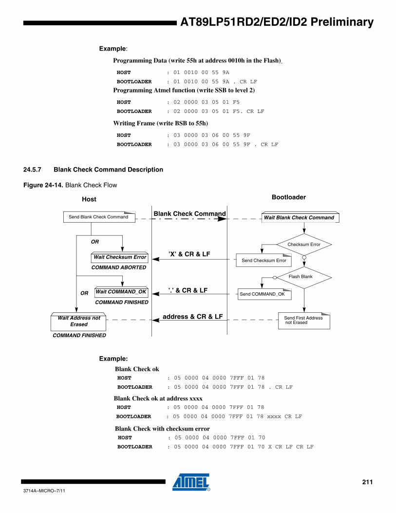
AT89LP51RD2/ED2/ID2 Preliminary
Example:
24.5.7 Blank Check Command Description
Figure 24-14. Blank Check Flow
Example:
HOST : 01 0010 00 55 9A
BOOTLOADER : 01 0010 00 55 9A . CR LF
Programming Data (write 55h at address 0010h in the Flash)
HOST : 02 0000 03 05 01 F5
BOOTLOADER : 02 0000 03 05 01 F5. CR LF
Programming Atmel function (write SSB to level 2)
HOST : 03 0000 03 06 00 55 9F
BOOTLOADER : 03 0000 03 06 00 55 9F . CR LF
Writing Frame (write BSB to 55h)
Host Bootloader
Blank Check Command
’X’ & CR & LF
Flash Blank
Wait Blank Check Command
Send First Address
Send COMMAND_OK
Send Blank Check Command
Wait Checksum Error
Wait Address notErased
Wait COMMAND_OK
OR
COMMAND ABORTED
COMMAND FINISHED
Send Checksum Error
COMMAND FINISHED
’.’ & CR & LFOR
address & CR & LF not Erased
Checksum Error
HOST : 05 0000 04 0000 7FFF 01 78
BOOTLOADER : 05 0000 04 0000 7FFF 01 78 . CR LF
Blank Check ok
BOOTLOADER : 05 0000 04 0000 7FFF 01 70 X CR LF CR LF
Blank Check with checksum errorHOST : 05 0000 04 0000 7FFF 01 70
BOOTLOADER : 05 0000 04 0000 7FFF 01 78 xxxx CR LF
Blank Check ok at address xxxxHOST : 05 0000 04 0000 7FFF 01 78
2113714A–MICRO–7/11

24.5.8 Display Data Description
Figure 24-15. Display Flow
Example:
Host Bootloader
Display Command
’X’ & CR & LF
RD_WR_SECURITY
Wait Display Command
Read Data
Send Security Error
Send Display Data
Send Display Command
Wait Checksum Error
Wait Display Data
Wait Security Error
OR
COMMAND ABORTED
COMMAND FINISHED
Send Checksum Error
COMMAND ABORTED
’L’ & CR & LFOR
"Address = "
All Data Read
Complet Frame
"Reading Value"CR & LF
All Data ReadAll Data Read
COMMAND FINISHED
Checksum error
HOST : 05 0000 04 0000 0020 00 D7
BOOTLOADER : 05 0000 04 0000 0020 00 D7 CR LF
BOOTLOADER 0000=-----data------ CR LF (16 data)
BOOTLOADER 0010=-----data------ CR LF (16 data)
BOOTLOADER 0020=data CR LF ( 1 data)
Display data from address 0000h to 0020h
2123714A–MICRO–7/11
AT89LP51RD2/ED2/ID2 Preliminary

AT89LP51RD2/ED2/ID2 Preliminary
24.5.9 Read Function DescriptionThis flow is similar for the following frames:
• Reading Frame
• EOF Frame/ Atmel Frame (only reading Atmel Frame)
Figure 24-16. Read Flow
Example:
Host Bootloader
Read Command
’X’ & CR & LF
RD_WR_SECURITY
Wait Read Command
Read Value
Send Security error
Send Data Read
Send Read Command
Wait Checksum Error
Wait Value of Data
Wait Security Error
OR
COMMAND ABORTED
COMMAND FINISHED
Send Checksum error
COMMAND ABORTED
’L’ & CR & LFOR
’value’ & ’.’ & CR & LF
Checksum error
HOST : 02 0000 05 07 02 F0
BOOTLOADER : 02 0000 05 07 02 F0 Value . CR LF
HOST : 02 0000 01 02 00 FB
BOOTLOADER : 02 0000 01 02 00 FB Value . CR LF
Read function (read SBV)
Atmel Read function (read Bootloader version)
2133714A–MICRO–7/11

24.5.10 Bootloader Command Summary
Note: 1. AT89C51ID2 Only. This byte differs from AT89C51ID2, which uses 02h
Table 24-19. Bootloader Command Summary
Command Command Name Data[0] Data[1] Command Effect
00h Program CodeProgram Nb Code Byte.
Bootloader will accept up to 128 (80h) data bytes. The data bytes should be 128 byte page flash boundary.
03h Write Function
01h
00h Erase block0 (0000h-1FFFh)
20h Erase block1 (2000h-3FFFh)
40h Erase block2 (4000h-7FFFh)
80h Erase block3 (8000h- BFFFh)
C0h Erase block4 (C000h- FFFFh)
03h 00h Hardware Reset
04h 00h Erase SBV & BSB
05h00h Program SSB level 1
01h Program SSB level 2
06h00h Program BSB (value to write in data[2])
01h Program SBV (value to write in data[2])
07h -Full Chip Erase (This command needs about 6 sec to be
executed)
0Ah
10h(1) Program OSC fuse (value to write in data[2])
04h Program BLJB fuse (value to write in data[2])
08h Program X2 fuse (value to write in data[2])
04h Display Function
Data[0:1] = start address
Data [2:3] = end address
Data[4] = 00h:Display Code
Data[4] = 01h: Blank check
Data[4] = 02h: Display EEPROM
Display Code
Blank Check
Display EEPROM data
05h Read Function
00h
00h Manufacturer Id
01h Device Id #1
02h Device Id #2
03h Device Id #3
07h
00h Read SSB
01h Read BSB
02h Read SBV
06h Read Extra Byte
0Bh 00h Read Hardware Byte
0Eh00h Read Device Boot ID1
01h Read Device Boot ID2
0Fh 00h Read Bootloader Version
07h Program EEPROM dataProgram Nn EEprom Data Byte.
Bootloader will accept up to 128 (80h) data bytes.
2143714A–MICRO–7/11
AT89LP51RD2/ED2/ID2 Preliminary

AT89LP51RD2/ED2/ID2 Preliminary
24.6 In-System Programming (ISP)The Atmel AT89LP51RD2/ED2/ID2 microcontroller features 64K bytes of on-chip In-SystemProgrammable Flash program memory and 4K bytes of nonvolatile EPROM data memory. In-System Programming allows programming and reprogramming of the microcontroller positionedinside the end system. Using a simple 4-wire SPI interface, the programmer communicates seri-ally with the AT89LP51RD2/ED2/ID2 microcontroller, reprogramming all nonvolatile memorieson the chip. In-System Programming eliminates the need for physical removal of the chips fromthe system. This will save time and money, both during development in the lab, and when updat-ing the sof twa re or pa rameters in the f ie ld . The programming in ter face o f theAT89LP51RD2/ED2/ID2 includes the following features:
• Four-wire serial SPI Programming Interface or 12-pin Parallel Interface
• Selectable Polarity Reset Entry into Programming
• User Signature Array
• Flexible Page Programming
• Row Erase Capability
• Page Write with Auto-Erase Commands
• Programming Status Register
For more detailed information on In-System Programming, refer to the Application Note entitled“AT89LP In-System Programming Specification”.
24.6.1 Physical InterfaceThe AT89LP51RD2/ED2/ID2 provides a standard programming command set with two physicalinterfaces: a bit-serial and a byte-parallel interface. Normal Flash programming utilizes the SerialPeripheral Interface (SPI) pins of an AT89LP51RD2/ED2/ID2 microcontroller. The SPI is a full-duplex synchronous serial interface consisting of four wires: Serial Clock (SCK), Master-In/Slave-out (MISO), Master-out/Slave-in (MOSI) and Slave Select (SS). When programming anAT89LP51RD2/ED2/ID2 device, the programmer always operates as the SPI master, and thetarget system always operates as the SPI slave. To enter or remain in Programming mode thedevice’s reset line (RST) must be held active. With the addition of VDD and GND, anAT89LP51RD2/ED2/ID2 microcontroller can be programmed with a minimum of eight connec-tions as shown in Figure 24-17.
Figure 24-17. In-System Programming Device Connections
AT89LP51RD2/ED2/ID2
VDD
RST
P1.7/SCK
P1.5/MOSI
GND
Serial Clock
Serial In
RST
P1.4/SS
P1.6/MISO Serial Out
SS POL GND or VDD
2153714A–MICRO–7/11

The Parallel interface is a special mode of the serial interface, i.e. the serial interface is used toenable the parallel interface. After enabling the interface serially over P1.7/SCK and P1.5/MOSI,P1.5 is reconfigured as an active-low output enable (OE) for data on Port 0. When OE = 1, com-mand, address and write data bytes are input on Port 0 and sampled at the rising edge of SCK.When OE = 0, read data bytes are output on Port 0 and should be sampled on the falling edge ofSCK. The P1.7/SCK and RST pins continue to function in the same manner. With the addition ofVDD and GND, the parallel interface requires a minimum of fourteen connections as shown inFigure 24-18. Note that a connection to P1.6/MISO is not required for using the parallelinterface.
Figure 24-18. Parallel Programming Device Connections
The Programming Interface is a means of externally programming the AT89LP51RD2/ED2/ID2microcontroller. The Interface can be used to program the device both in-system and in a stand-alone serial programmer. The Interface does not require any clock other than SCK and is notlimited by the system clock frequency. During Programming the system clock source of the tar-get device can operate normally.
When designing a system where In-System Programming will be used, the following observa-tions must be considered for correct operation:
• The ISP interface uses the SPI clock mode 0 (CPOL = 0, CPHA = 0) exclusively with a maximum frequency of 5 MHz.
• The AT89LP51RD2/ED2/ID2 will enter programming mode only when its reset line (RST) is active. To simplify this operation, it is recommended that the target reset can be controlled by the In-System programmer. To avoid problems, the In-System programmer should be able to keep the entire target system reset for the duration of the programming cycle. The target system should never attempt to drive the three SPI lines while reset is active.
• The ISP Enable Fuse must be set to allow programming during any reset period. If the ISP Fuse is disabled, ISP may only be entered at POR. To enter programming the RST pin must be driven active prior to the end of Power-On Reset (POR). After POR has completed the device will remain in ISP mode until RST is brought inactive. Once the initial ISP session has ended, the power to the target device must be cycled OFF and ON to enter another session. Note that if this method is required, an active-low reset polarity is recommended.
• For standalone programmers, an active-low reset polarity is recommended (POL = 0). RST may then be tied directly to GND to ensure correct entry into Programming mode regardless of the device settings.
AT89LP51RD2/ED2/ID2
VDD RST
P1.7/SCK
P1.5/MOSI
GND
Clock
OE
RST
P1.4/SS SS
P0.7-0 Data In/Out 8
POL GND or VDD
2163714A–MICRO–7/11
AT89LP51RD2/ED2/ID2 Preliminary

AT89LP51RD2/ED2/ID2 Preliminary
24.6.2 Command FormatProgramming commands consist of two preamble bytes, an opcode byte, two address bytes,and zero or more data bytes. Figure 24-19 on page 217 shows a simplified flow chart of a com-mand sequence.
A sample command packet is shown in Figure 24-20 on page 218. The SS pin defines thepacket frame. SS must be brought low before the first byte in a command is sent and broughtback high after the final byte in the command has been sent. The command is not complete untilSS returns high. Command bytes are issued serially on MOSI. Data output bytes are receivedserially on MISO. Packets of variable length are supported by returning SS high when the finalrequired byte has been transmitted. In some cases command bytes have a don’t care value.Don’t care bytes in the middle of a packet must be transmitted. Don’t care bytes at the end of apacket may be ignored.
Page oriented instructions always include a full 16-bit address. The higher order bits select thepage and the lower order bits select the byte within that page. The AT89LP51RD2/ED2/ID2 allo-cates 6 bits for byte address, 1 bit for low/high half page selection and 9 bits for page address.The half page to be accessed is always fixed by the page address and half select as transmitted.The byte address specifies the starting address for the first data byte. After each data byte hasbeen transmitted, the byte address is incremented to point to the next data byte. This allows apage command to linearly sweep the bytes within a page. If the byte address is incrementedpast the last byte in the half page, the byte address will roll over to the first byte in the same halfpage. While loading bytes into the page buffer, overwriting previously loaded bytes will result indata corruption.
For a summary of available commands, see Table 24-20 on page 219.
Figure 24-19. Command Sequence Flow Chart
Input Preamble 2(55h)
Input Opcode
Input AddressHigh Byte
Input AddressLow Byte
Input/OutputData
Address +1
Input Preamble 1(AAh)
2173714A–MICRO–7/11
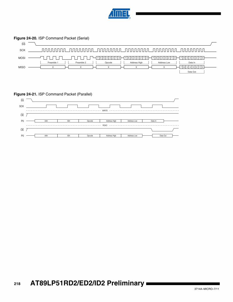
Figure 24-20. ISP Command Packet (Serial)
Figure 24-21. ISP Command Packet (Parallel)
7 06 5 4 3 2 1 7 06 5 4 3 2 1 7 06 5 4 3 2 1 7 06 5 4 3 2 1
7 06 5 4 3 2 1
SS
SCK
MOSI
MISO
Preamble 2 Opcode Address High Address Low Data In
Data Out
X X X X
Preamble 1
X
SS
SCK
P0 55h Opcode Address High Address LowAAh Data In
OE
WRITE
P0 55h Opcode Address High Address LowAAh Data Out
OE
READ
2183714A–MICRO–7/11
AT89LP51RD2/ED2/ID2 Preliminary

AT89LP51RD2/ED2/ID2 Preliminary
Notes: 1. Program Enable must be the first command issued after entering into programming mode.
2. Parallel Enable switches the interface from serial to parallel format until RST returns high.
3. Any number of Data bytes from 1 to 64 may be written/read. The internal address is incremented between each byte.
4. Each byte address selects one fuse or lock bit. Data bytes must be 00h or FFh.
5. See Table 24-5 on page 190 for Fuse definitions.
6. See Table 24-6 on page 192 for Lock Bit definitions.
7. Symbol Key:
Table 24-20. Programming Command Summary
Command Opcode Addr High Addr Low Data 0 Data n
Program Enable(1) 1010 1100 0101 0011 – – –
Parallel Enable(2) 1010 1100 0011 0101 – – –
Chip Erase 1000 1010 – – – –
Read Status 0110 0000 xxxx xxxx xxxx xxxx Status Out
Load Page Buffer(3) 0101 0001 xxxx xxxx 00bb bbbb Data In 0 ... Data In n
Write Code Page(3) 0101 0000 aaaa aaaa asbb bbbb Data In 0 ... Data In n
Write Code Page with Auto-Erase(3) 0111 0000 aaaa aaaa asbb bbbb Data In 0 ... Data In n
Read Code Page(3) 0011 0000 aaaa aaaa asbb bbbb Data Out 0 ... Data Out n
Write Data Page(3) 1101 0000 000a aaaa asbb bbbb Data In 0 ... Data In n
Write Data Page with Auto-Erase(3) 1101 0010 000a aaaa asbb bbbb Data In 0 ... Data In n
Read Data Page(3) 1011 0000 000a aaaa asbb bbbb Data Out 0 ... Data Out n
Write User Fuses(3)(4)(5) 1110 0001 0000 0000 00bb bbbb Data In 0 ... Data In n
Write User Fuses with Auto-Erase(3)(4)(5) 1111 0001 0000 0000 00bb bbbb Data In 0 ... Data In n
Read User Fuses(3)(4)(5) 0110 0001 0000 0000 00bb bbbb Data Out 0 ... Data Out n
Write Lock Bits(3)(4)(6) 1110 0100 0000 0000 00bb bbbb Data In 0 ... Data In n
Read Lock Bits(3)(4)(6) 0110 0100 0000 0000 00bb bbbb Data Out 0 ... Data Out n
Write User Signature Page(3) 0101 0010 0000 0000 asbb bbbb Data In 0 ... Data In n
Write User Signature Page with Auto-Erase(3) 0111 0010 0000 0000 asbb bbbb Data In 0 ... Data In n
Read User Signature Page(3) 0011 0010 0000 0000 asbb bbbb Data Out 0 ... Data Out n
Read Atmel Signature Page(3) 0011 1000 0000 0000 0sbb bbbb Data Out 0 ... Data Out n
a: Page Address Bit
s: Half Page Select Bit
b: Byte Address Bit
x: Don’t Care Bit
2193714A–MICRO–7/11

24.6.3 Status RegisterThe current state of the memory may be accessed by reading the status register. The status reg-ister is shown in Table 24-21.
24.6.4 DATA PollingThe AT89LP51RD2/ED2/ID2 implements DATA polling to indicate the end of a programmingcycle. While the device is busy, any attempted read of the last byte written will return the databyte with the MSB complemented. Once the programming cycle has completed, the true valuewill be accessible. During Erase the data is assumed to be FFH and DATA polling will return7FH. When writing multiple bytes in a page, the DATA value will be the last data byte loadedbefore programming begins, not the written byte with the highest physical address within thepage.
24.6.5 Programming Interface TimingThis section details general system timing sequences and constraints for entering or exiting In-System Programming as well as parameters related to the Serial Peripheral Interface duringISP. The general timing parameters for the following waveform figures are listed in section “Tim-ing Parameters” on page 223.
24.6.5.1 Power-up SequenceExecute this sequence to enter programming mode immediately after power-up. In the RST pinis disabled or if the ISP Fuse is disabled, this is the only method to enter programming (see“External Reset” on page 55).
1. Apply power between VDD and GND pins. RST should remain low.
2. Wait at least tPWRUP. and drive RST high if active-high otherwise keep low.
3. Wait at least tSUT for the internal Power-on Reset to complete. The value of tSUT will depend on the current settings of the device.
4. Start programming session.
Table 24-21. Status Register
– – – – LOAD SUCCESS WRTINH BUSY
Bit 7 6 5 4 3 2 1 0
Symbol Function
LOADLoad flag. Cleared low by the load page buffer command and set high by the next memory write. This flag signals that the page buffer was previously loaded with data by the load page buffer command.
SUCCESSSuccess flag. Cleared low at the start of a programming cycle and will only be set high if the programming cycle completes without interruption from the brownout detector.
WRTINHWrite Inhibit flag. Cleared low by the brownout detector (BOD) whenever programming is inhibited due to VDD falling below the minimum required programming voltage. If a BOD episode occurs during programming, the SUCCESS flag will remain low after the cycle is complete.
BUSY Busy flag. Cleared low whenever the memory is busy programming or if write is currently inhibited.
2203714A–MICRO–7/11
AT89LP51RD2/ED2/ID2 Preliminary
AT89LP51RD2/ED2/ID2 Preliminary
Figure 24-22. Serial Programming Power-up Sequence
24.6.5.2 Power-down Sequence Execute this sequence to power-down the device after programming.
1. Drive SCK low.
2. Wait at least tSSD and Tristate MOSI.
3. Wait at least tRHZ and drive RST low.
4. Wait at least tSSZ and tristate SCK.
5. Wait no more than tPWRDN and power off VDD.
Figure 24-23. Serial Programming Power-down Sequence
24.6.5.3 ISP Start Sequence Execute this sequence to exit CPU execution mode and enter ISP mode when the device haspassed Power-On Reset and is already operational.
1. Drive RST high.
2. Wait tRLZ + tSTL.
3. Drive SCK low.
4. Start programming session.
VDD
RST
SS
SCK
HIGH ZMISO
HIGH ZMOSI
tPWRUP
tPOR + tSUT tZSS
VDD
RST
SS
SCK
HIGH ZMISO
HIGH ZMOSI
tPWRDN
tSSD tSSZ
2213714A–MICRO–7/11

Figure 24-24. In-System Programming (ISP) Start Sequence
24.6.5.4 ISP Exit Sequence Execute this sequence to exit ISP mode and resume CPU execution mode.
1. Drive SCK low.
1. Wait at least tSSD.
2. Tristate MOSI.
3. Wait at least tRHZ and bring RST low.
4. Wait tSSZ and tristate SCK.
Figure 24-25. In-System Programming (ISP) Exit Sequence
Note: The waveforms on this page are not to scale.
24.6.5.5 Serial Peripheral InterfaceThe Serial Peripheral Interface (SPI) is a byte-oriented full-duplex synchronous serial communi-cation channel. During In-System Programming, the programmer always acts as the SPI masterand the target device always acts as the SPI slave. The target device receives serial data onMOSI and outputs serial data on MISO. The Programming Interface implements a standardSPI Port with a fixed data order and For In-System Programming, bytes are transferred MSBfirst as shown in Figure 24-26. The SCK phase and polarity follow SPI clock mode 0 (CPOL = 0,CPHA = 0) where bits are sampled on the rising edge of SCK and output on the falling edge ofSCK. For more detailed timing information see Figure 24-27.
tSTL
VDD
RST
SS
SCK
HIGH ZMOSI
HIGH ZMISO
XTAL1
tRLZ
tZSS
tSSE
VDD
RST
SS
SCK
HIGH ZMOSI
HIGH ZMISO
XTAL1
tSSZ
tSSD
tRHZ
2223714A–MICRO–7/11
AT89LP51RD2/ED2/ID2 Preliminary

AT89LP51RD2/ED2/ID2 Preliminary
Figure 24-26. ISP Byte Sequence
Figure 24-27. Serial Programming Interface Timing
Figure 24-28. Parallel Programming Interface Timing
24.6.6 Timing ParametersThe timing parameters for Figure 24-22, Figure 24-23, Figure 24-24, Figure 24-25, Figure 24-27and Figure 24-28 are shown in Table .
7
7
6
6
5
5
4
4
3
3
2
2
1
1
0
0
MOSI
MISO
SCK
Data Sampled
tSRtSSE
tSLSH
tSOV
tSF
tSOX
tSSDtSCK
tSHSL
tSOE tSOH
tSIHtSIS
SS
SCK
MISO
MOSI
tSRtSSE
tSLSH
tSF
tPOX
tSSDtSCK
tSHSL
tPOVtPOE
tPIHtPIS
SS
SCK
P0
OE
tPOH
2233714A–MICRO–7/11

Note: 1. tSCK is independent of tCLCL.
Table 24-22. Programming Interface Timing Parameters
Symbol Parameter Min Max Units
tCLCL System Clock Cycle Time 0 60 ns
tPWRUP Power On to SS High Time 10 µs
tPOR Power-on Reset Time 100 µs
tPWRDN SS Tristate to Power Off 1 µs
tRLZ RST Low to I/O Tristate tCLCL 2 tCLCL ns
tSTL RST Low Settling Time 100 ns
tRHZ RST High to SS Tristate 0 2 tCLCL ns
tSCK Serial Clock Cycle Time 200(1) ns
tSHSL Clock High Time 75 ns
tSLSH Clock Low Time 50 ns
tSR Rise Time 25 ns
tSF Fall Time 25 ns
tSIS Serial Input Setup Time 10 ns
tSIH Serial Input Hold Time 10 ns
tSOH Serial Output Hold Time 10 ns
tSOV Serial Output Valid Time 35 ns
tPIS Parallel Input Setup Time 10 ns
tPIH Parallel Input Hold Time 10 ns
tPOH Parallel Output Hold Time 10 ns
tPOV Parallel Output Valid Time 35 ns
tSOE Serial Output Enable Time 10 ns
tSOX Serial Output Disable Time 25 ns
tPOE Parallel Output Enable Time 10 ns
tPOX Parallel Output Disable Time 25 ns
tSSE SS Active Lead Time tSLSH ns
tSSD SS Inactive Lag Time tSLSH ns
tZSS SCK Setup to SS Low 25 ns
tSSZ SCK Hold after SS High 25 ns
tWR Write Cycle Time 2.5 ms
tAWR Write Cycle with Auto-Erase Time 5 ms
tERS Chip Erase Cycle Time 7.5 ms
2243714A–MICRO–7/11
AT89LP51RD2/ED2/ID2 Preliminary
AT89LP51RD2/ED2/ID2 Preliminary
25. Electrical Characteristics
Notes: 1. Under steady state (non-transient) conditions, IOL must be externally limited as follows:Maximum IOL per port pin: 10 mAMaximum total IOL for all output pins: 15 mAIf IOL exceeds the test condition, VOL may exceed the related specification. Pins are not guaranteed to sink current greater than the listed test conditions.
2. Minimum VDD for Power-down is 2V.
3. All characteristics contained in this datasheet are based on simulation and characterization of other microcontrollers manu-factured in the same process technology. These values are preliminary values representing design targets, and will be updated after characterization of actual silicon.
25.1 Absolute Maximum Ratings*
Operating Temperature ................................... -40°C to +85°C *NOTICE: Stresses beyond those listed under “Absolute Maximum Ratings” may cause permanent dam-age to the device. This is a stress rating only and functional operation of the device at these or any other conditions beyond those indicated in the operational sections of this specification is not implied. Exposure to absolute maximum rating conditions for extended periods may affect device reliability.
Storage Temperature ..................................... -65°C to +150°C
Voltage on Any Pin with Respect to Ground......-0.7V to +5.5V
Maximum Operating Voltage ............................................ 5.5V
DC Output Current...................................................... 15.0 mA
25.2 DC CharacteristicsTA = -40°C to 85°C, VDD = 2.4V to 5.5V (unless otherwise noted)
Symbol Parameter Condition Min Max Units
VIL Input Low-voltage -0.5 0.2 VDD - 0.1 V
VIH Input High-voltage 0.2 VDD + 0.9 VDD + 0.5 V
VOL Output Low-voltage(1) IOL = 10 mA, VDD = 2.7V, TA = 85°C 0.5 V
VOHOutput High-voltageWith Weak Pull-ups Enabled
IOH = -80 µA, VDD = 3V ± 10% 2.4 V
IOH = -30 µA 0.75 VDD V
IOH = -12 µA 0.9 VDD V
VOH1Output High-voltageWith Strong Pull-ups Enabled
IOH = -10 mA, TA = 85°C 0.9 VDD
IOH = -5 mA, TA = 85°C 0.75 VDD
IIL Logic 0 Input Current VIN = 0.45V -50 µA
ITL Logic 1 to 0 Transition Current VIN = 2V, VDD = 5V ± 10% -750 µA
ILI Input Leakage Current 0 < VIN < VDD ±10 µA
RRST Reset Pull-up Resistor 50 150 kΩ
CIO Pin Capacitance Test Freq. = 1 MHz, TA = 25°C 10 pF
ICC
Power Supply Current
Active Mode, 12 MHz, VDD = 5.5V 7 mA
Idle Mode, 12 MHz, VDD = 5.5V
P1.0 & P1.1 = 0V or VDD
3 mA
Power-down Mode(2)VDD = 5.5V, P1.0 & P1.1 = 0V or VDD 5 µA
VDD = 3V, P1.0 & P1.1 = 0V or VDD 2 µA
2253714A–MICRO–7/11

25.3 Typical CharacteristicsThe following charts show typical behavior. These figures are not tested during manufacturing.All current consumption measurements are performed with all I/O pins configured as quasi-bidi-rectional (with internal pull-ups). A square wave generator with rail-to-rail output is used as anexternal clock source for consumption versus frequency measurements.
25.3.1 Supply Current (Internal Oscillator)
Figure 25-1. Active Supply Current vs. Vcc (8.0 MHz Internal Oscillator)
Figure 25-2. Idle Supply Current vs. Vcc (8.0 MHz Internal Oscillator)
2.4 2.7 3.0 3.3 3.63.5
4.0
4.5
5.0
5.5
6.0
6.585C
-40C
25C
Vcc (V)
Icc
(mA
) Active Supply Current vs. Vcc
8MHz Internal Oscillator
2.4 2.7 3.0 3.3 3.61.00
1.25
1.50
1.75
2.0085C
-40C
25C
Vcc (V)
Icc
(mA
)
Idle Supply Current vs. Vcc 8MHz Internal Oscillator
2263714A–MICRO–7/11
AT89LP51RD2/ED2/ID2 Preliminary

AT89LP51RD2/ED2/ID2 Preliminary
25.3.2 Supply Current (External Clock)
Figure 25-3. Active Supply Current vs. Frequency
Figure 25-4. Idle Supply Current vs. Frequency
Note: All characteristics contained in this datasheet are based on simulation and characterization of other microcontrollers manufactured in the same process technology. These values are prelimi-nary values representing design targets, and will be updated after characterization of actual silicon.
0 5 10 15 20 250
2
4
6
8
10
12
14
16
18
205.5V
5.0V
4.5V
3.6V
3.0V
2.4V
Frequency (MHz)
Icc
(mA
)
Active Supply Current vs. FrequencyExternal Clock Source
0 5 10 15 20 250
1
2
3
4
5
6
75.5V
5.0V
4.5V
3.6V
3.0V
2.4V
Frequency (MHz)
Icc
(mA
)
Idle Supply Current vs. FrequencyExternal Clock Source
2273714A–MICRO–7/11

25.4 Clock CharacteristicsThe values shown in this table are valid for TA = -40°C to 85°C and VDD = 2.4 to 5.5V, unless otherwise noted.
Figure 25-5. External Clock Drive Waveform
Table 25-1. External Clock Parameters
Symbol Parameter
VDD = 2.4V to 5.5V VDD = 4.5V to 5.5V
UnitsMin Max Min Max
1/tCLCL Oscillator Frequency 0 20 0 25 MHz
tCLCL Clock Period 50 40 ns
tCHCX External Clock High Time 12 ns
tCLCX External Clock Low Time 12 ns
tCLCH External Clock Rise Time 5 ns
tCHCL External Clock Fall Time 5 ns
Table 25-2. Clock Characteristics
Symbol Parameter Condition Min Max Units
fXTAL Crystal Oscillator FrequencyLow Power Oscillator 0 12 MHz
High Power Oscillator 0 24 MHz
fRC Internal Oscillator FrequencyTA = 25°C; VDD = 5.0V 7.92 8.08 MHz
VDD = 2.4 to 5.5V 7.80 8.20 MHz
2283714A–MICRO–7/11
AT89LP51RD2/ED2/ID2 Preliminary
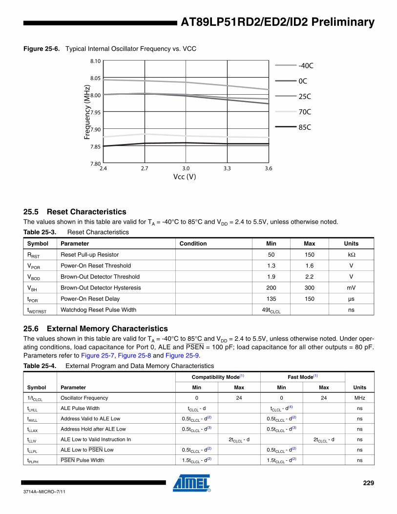
AT89LP51RD2/ED2/ID2 Preliminary
Figure 25-6. Typical Internal Oscillator Frequency vs. VCC
25.5 Reset CharacteristicsThe values shown in this table are valid for TA = -40°C to 85°C and VDD = 2.4 to 5.5V, unless otherwise noted.
25.6 External Memory CharacteristicsThe values shown in this table are valid for TA = -40°C to 85°C and VDD = 2.4 to 5.5V, unless otherwise noted. Under oper-ating conditions, load capacitance for Port 0, ALE and PSEN = 100 pF; load capacitance for all other outputs = 80 pF.Parameters refer to Figure 25-7, Figure 25-8 and Figure 25-9.
2.4 2.7 3.0 3.3 3.67.80
7.85
7.90
7.95
8.00
8.05
8.10-40C
0C
25C
70C
85C
Vcc (V)
Freq
uen
cy (M
Hz)
Table 25-3. Reset Characteristics
Symbol Parameter Condition Min Max Units
RRST Reset Pull-up Resistor 50 150 kΩ
VPOR Power-On Reset Threshold 1.3 1.6 V
VBOD Brown-Out Detector Threshold 1.9 2.2 V
VBH Brown-Out Detector Hysteresis 200 300 mV
tPOR Power-On Reset Delay 135 150 µs
tWDTRST Watchdog Reset Pulse Width 49tCLCL ns
Table 25-4. External Program and Data Memory Characteristics
Symbol Parameter
Compatibility Mode(1) Fast Mode(1)
UnitsMin Max Min Max
1/tCLCL Oscillator Frequency 0 24 0 24 MHz
tLHLL ALE Pulse Width tCLCL - d tCLCL - d(4) ns
tAVLL Address Valid to ALE Low 0.5tCLCL - d(2) 0.5tCLCL - d
(2) ns
tLLAX Address Hold after ALE Low 0.5tCLCL - d(3) 0.5tCLCL - d
(3) ns
tLLIV ALE Low to Valid Instruction In 2tCLCL - d 2tCLCL - d ns
tLLPL ALE Low to PSEN Low 0.5tCLCL - d(2) 0.5tCLCL - d
(2) ns
tPLPH PSEN Pulse WIdth 1.5tCLCL - d(2) 1.5tCLCL - d
(2) ns
2293714A–MICRO–7/11
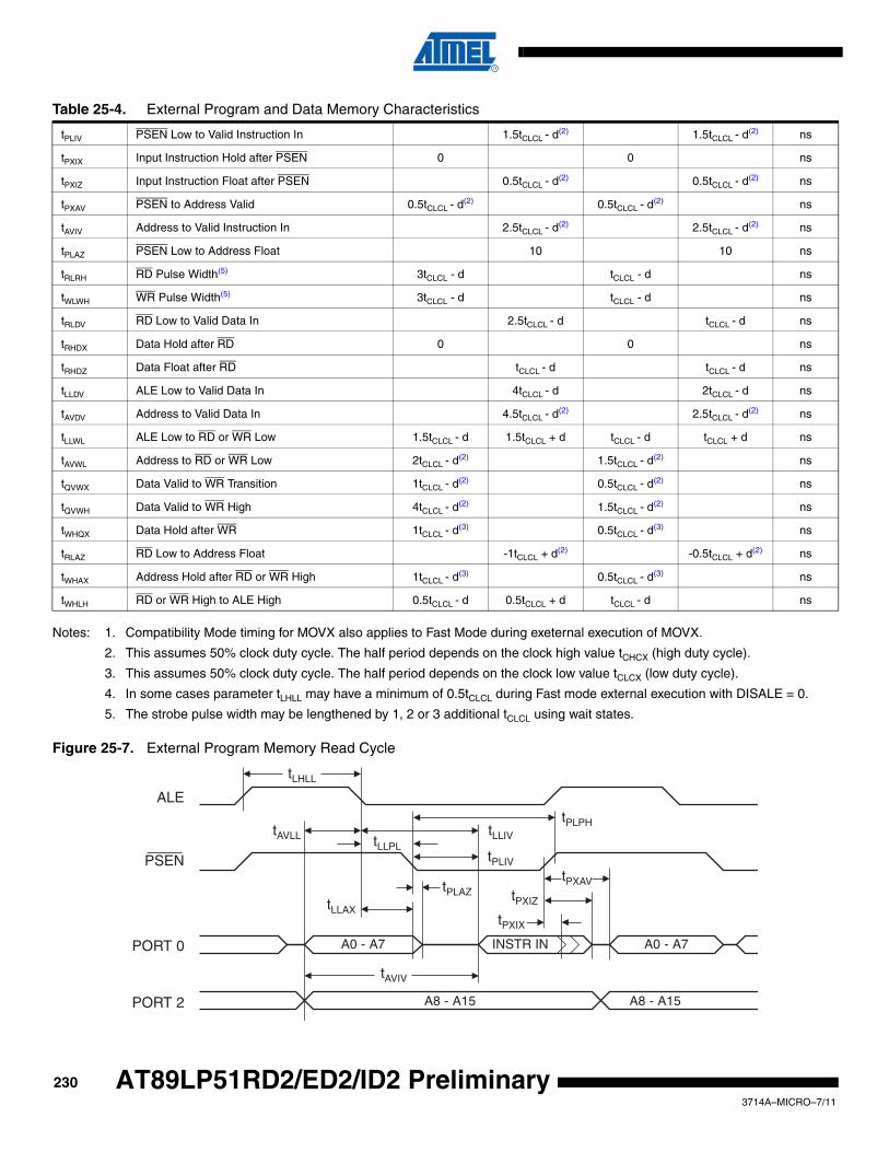
Notes: 1. Compatibility Mode timing for MOVX also applies to Fast Mode during exeternal execution of MOVX.
2. This assumes 50% clock duty cycle. The half period depends on the clock high value tCHCX (high duty cycle).
3. This assumes 50% clock duty cycle. The half period depends on the clock low value tCLCX (low duty cycle).
4. In some cases parameter tLHLL may have a minimum of 0.5tCLCL during Fast mode external execution with DISALE = 0.
5. The strobe pulse width may be lengthened by 1, 2 or 3 additional tCLCL using wait states.
Figure 25-7. External Program Memory Read Cycle
tPLIV PSEN Low to Valid Instruction In 1.5tCLCL - d(2) 1.5tCLCL - d
(2) ns
tPXIX Input Instruction Hold after PSEN 0 0 ns
tPXIZ Input Instruction Float after PSEN 0.5tCLCL - d(2) 0.5tCLCL - d
(2) ns
tPXAV PSEN to Address Valid 0.5tCLCL - d(2) 0.5tCLCL - d
(2) ns
tAVIV Address to Valid Instruction In 2.5tCLCL - d(2) 2.5tCLCL - d
(2) ns
tPLAZ PSEN Low to Address Float 10 10 ns
tRLRH RD Pulse Width(5) 3tCLCL - d tCLCL - d ns
tWLWH WR Pulse Width(5) 3tCLCL - d tCLCL - d ns
tRLDV RD Low to Valid Data In 2.5tCLCL - d tCLCL - d ns
tRHDX Data Hold after RD 0 0 ns
tRHDZ Data Float after RD tCLCL - d tCLCL - d ns
tLLDV ALE Low to Valid Data In 4tCLCL - d 2tCLCL - d ns
tAVDV Address to Valid Data In 4.5tCLCL - d(2) 2.5tCLCL - d
(2) ns
tLLWL ALE Low to RD or WR Low 1.5tCLCL - d 1.5tCLCL + d tCLCL - d tCLCL + d ns
tAVWL Address to RD or WR Low 2tCLCL - d(2) 1.5tCLCL - d
(2) ns
tQVWX Data Valid to WR Transition 1tCLCL - d(2) 0.5tCLCL - d
(2) ns
tQVWH Data Valid to WR High 4tCLCL - d(2) 1.5tCLCL - d
(2) ns
tWHQX Data Hold after WR 1tCLCL - d(3) 0.5tCLCL - d
(3) ns
tRLAZ RD Low to Address Float -1tCLCL + d(2) -0.5tCLCL + d(2) ns
tWHAX Address Hold after RD or WR High 1tCLCL - d(3) 0.5tCLCL - d
(3) ns
tWHLH RD or WR High to ALE High 0.5tCLCL - d 0.5tCLCL + d tCLCL - d ns
Table 25-4. External Program and Data Memory Characteristics
tLHLL
tLLIV
tPLIV
tLLAXtPXIZ
tPLPH
tPLAZtPXAV
tAVLL tLLPL
tAVIV
tPXIX
ALE
PSEN
PORT 0
PORT 2 A8 - A15
A0 - A7 A0 - A7
A8 - A15
INSTR IN
2303714A–MICRO–7/11
AT89LP51RD2/ED2/ID2 Preliminary

AT89LP51RD2/ED2/ID2 Preliminary
Figure 25-8. External Data Memory Read Cycle
Figure 25-9. External Data Memory Write Cycle
25.7 Serial Peripheral Interface TimingThe values shown in these tables are valid for TA = -40°C to 85°C and VDD = 2.4 to 5.5V, unless otherwise noted.
Table 25-5. SPI Master Characteristics
Symbol Parameter Min Max Units
tCLCL Oscillator Period 41.6 ns
tSCK Serial Clock Cycle Time 4tCLCL ns
tSHSL Clock High Time tSCK/2 - 25 ns
tSLSH Clock Low Time tSCK/2 - 25 ns
tSR Rise Time 25 ns
tSF Fall Time 25 ns
tSIS Serial Input Setup Time 10 ns
tLHLL
ALE
DATA INA0 - A7
A8 - A15 FROM DPH OR P2.0 - P2.7P2 P2
RD
PORT 0
PORT 2
tLLWL tRLRH
tAVLL tLLAX
tRLAZ tRHDZ
tAVWL
tWHLH
tWHAXtAVDV
tLLDV
tRLDV
tRHDX
tLHLL
ALE
DATA OUTA0 - A7
A8 - A15 FROM DPH OR P2.0 - P2.7P2 P2
WR
PORT 0
PORT 2
tLLWL tWLWH
tAVLL tLLAX
tQVWX
tQVWH
tWHQX
tAVWL
tWHLH
tWHAX
2313714A–MICRO–7/11

Figure 25-10. SPI Master Timing (CPHA = 0)
tSIH Serial Input Hold Time 10 ns
tSOH Serial Output Hold Time 10 ns
tSOV Serial Output Valid Time 35 ns
Table 25-5. SPI Master Characteristics
Symbol Parameter Min Max Units
Table 25-6. SPI Slave Characteristics
Symbol Parameter Min Max Units
tCLCL Oscillator Period 41.6 ns
tSCK Serial Clock Cycle Time 4tCLCL ns
tSHSL Clock High Time 1.5 tCLCL - 25 ns
tSLSH Clock Low Time 1.5 tCLCL - 25 ns
tSR Rise Time 25 ns
tSF Fall Time 25 ns
tSIS Serial Input Setup Time 10 ns
tSIH Serial Input Hold Time 10 ns
tSOH Serial Output Hold Time 10 ns
tSOV Serial Output Valid Time 35 ns
tSOE Output Enable Time 10 ns
tSOX Output Disable Time 25 ns
tSSE Slave Enable Lead Time 10 ns
tSSD Slave Disable Lag Time 0 ns
SS
SCK(CPOL = 0)
SCK(CPOL = 1)
MISO
MOSI
tSRtSCK
tSLSH
tSLSH
tSHSL
tSHSL
tSOH
tSF
tSIS tSIH
tSOV
2323714A–MICRO–7/11
AT89LP51RD2/ED2/ID2 Preliminary

AT89LP51RD2/ED2/ID2 Preliminary
Figure 25-11. SPI Slave Timing (CPHA = 0)
Figure 25-12. SPI Master Timing (CPHA = 1)
Figure 25-13. SPI Slave Timing (CPHA = 1)
tSRtSSE
tSLSH
tSHSL
tSOV
tSF
tSOX
tSSDtSCK
tSLSH
tSHSL
tSOE tSOH
tSIHtSIS
SS
SCK(CPOL = 0)
SCK(CPOL= 1)
MISO
MOSI
tSHSL tSLSH
tSHSLtSLSH
tSCK
tSOH
tSF tSR
tSIS
tSOV
tSIH
SS
SCK(CPOL = 0)
SCK(CPOL = 1)
MISO
MOSI
SS
SCK(CPOL = 0)
SCK(CPOL = 1)
MISO
MOSI
tSCKtSSE
tSHSL
tSHSLtSLSH
tSLSH
tSSD
tSIHtSIS
tSOE tSOV tSOH tSOX
tSF tSR
2333714A–MICRO–7/11

25.8 Two-wire Serial Interface CharacteristicsTable 25-7 describes the requirements for devices connected to the Two-wire Serial Bus. The AT89LP51RD2/ED2/ID2Two-wire Serial Interface meets or exceeds these requirements under the noted conditions. The values shown in this tableare valid for TA = -40°C to 85°C and VDD = 2.4 to 5.5V, unless otherwise noted.
Timing symbols refer to Figure 25-14.
Notes: 1. In AT89LP51RD2/ED2/ID2, this parameter is characterized and not 100% tested.
2. Required only for fSCL > 100 kHz.
Table 25-7. Two-wire Serial Bus Requirements
Symbol Parameter Condition Min Max Units
VIL Input Low-voltage -0.5 0.3 VDD V
VIH Input High-voltage 0.7 VDD VDD + 0.5 V
Vhys(1) Hysteresis of Schmitt Trigger Inputs 0.05 VDD
(2) – V
VOL(1) Output Low-voltage 3 mA sink current 0 0.4 V
tr(1) Rise Time for both SDA and SCL 20 + 0.1Cb
(3)(2) 300 ns
tof(1) Output Fall Time from VIHmin to VILmax 10 pF < Cb < 400 pF(3) 20 + 0.1Cb
(3)(2) 250 ns
tSP(1) Spikes Suppressed by Input Filter 0 50(2) ns
Ii Input Current each I/O Pin 0.1VDD < Vi < 0.9VDD -10 10 µA
Ci(1) Capacitance for each I/O Pin – 10 pF
fSCL SCL Clock Frequency fCK(4) > 16fSCL 0 400 kHz
Rp Value of Pull-up resistor
fSCL ≤ 100 kHz
fSCL > 100 kHz
tHD;STA Hold Time (repeated) START ConditionfSCL ≤ 100 kHz 4.0 – µs
fSCL > 100 kHz 0.6 – µs
tLOW Low Period of the SCL ClockfSCL ≤ 100 kHz 4.7 – µs
fSCL > 100 kHz 1.3 – µs
tHIGH High period of the SCL clockfSCL ≤ 100 kHz 4.0 – µs
fSCL > 100 kHz 0.6 – µs
tSU;STA Set-up time for a repeated START conditionfSCL ≤ 100 kHz 4.7 – µs
fSCL > 100 kHz 0.6 – µs
tHD;DAT Data hold timefSCL ≤ 100 kHz 0 3.45 µs
fSCL > 100 kHz 0 0.9 µs
tSU;DAT Data setup timefSCL ≤ 100 kHz 250 – ns
fSCL > 100 kHz 100 – ns
tSU;STO Setup time for STOP conditionfSCL ≤ 100 kHz 4.0 – µs
fSCL > 100 kHz 0.6 – µs
tBUFBus free time between a STOP and START condition
fSCL ≤ 100 kHz 4.7 – µs
VDD 0.4V–
3mA----------------------------- 1000ns
Cb------------------- Ω
VDD 0.4V–
3mA----------------------------- 300ns
Cb---------------- Ω
2343714A–MICRO–7/11
AT89LP51RD2/ED2/ID2 Preliminary
AT89LP51RD2/ED2/ID2 Preliminary
3. Cb = capacitance of one bus line in pF.
4. fCK = CPU clock frequency
Figure 25-14. Two-wire Serial Bus Timing
Figure 25-15. Shift Register Mode Timing Waveform
tSU;STA
tLOW
tHIGH
tLOW
tof
tHD;STA tHD;DAT tSU;DATtSU;STO
tBUF
SCL
SDA
tr
25.9 Serial Port Timing: Shift Register ModeThe values in this table are valid for VDD = 2.4V to 5.5V and Load Capacitance = 80 pF.
Symbol Parameter
SMOD1 = 0 SMOD1 = 1
UnitsMin Max Min Max
tXLXL Serial Port Clock Cycle Time 4tCLCL -15 2tCLCL -15 µs
tQVXH Output Data Setup to Clock Rising Edge 3tCLCL -15 tCLCL -15 ns
tXHQX Output Data Hold after Clock Rising Edge tCLCL -15 tCLCL -15 ns
tXHDX Input Data Hold after Clock Rising Edge 0 0 ns
tXHDV Input Data Valid to Clock Rising Edge 15 15 ns
0 1 2 3 4 5 6 7
ValidValidValidValid Valid Valid Valid Valid
Clock
Write to SBUF
Output Data
Clear RI
Input Data
SMOD1 = 0
0 1 2 3 4 5 6 7
ValidValidValidValid Valid Valid Valid Valid
Clock
Write to SBUF
Output Data
Clear RI
Input Data
SMOD1 = 1
2353714A–MICRO–7/11

25.10 Dual Analog Comparator CharacteristicsThe values shown in this table are valid for TA = -40°C to 85°C and VDD = 2.4 to 5.5V, unless otherwise noted.
Figure 25-16. Analog Reference Voltage Typical Characteristics
25.11 DADC CharacteristicsThe values shown in these tables are valid for TA = -40°C to 85°C and VDD = 2.4 to 5.5V, unless otherwise noted.
Table 25-8. Dual Analog Comparator Characteristics
Symbol Parameter Condition Min Max Units
VCM Common Mode Input Voltage GND VDD V
VOS Input Offset Voltage VDD = 3.6V 20 mV
VAREF Analog Reference Voltage 1.23 1.36 V
VΔREF Reference Delta Voltage 90 120 mV
tCMP Comparator Propagation Delay VIN+ – VIN- = 20mV; VDD = 2.4V 200 ns
tAREF Reference Settling Time 3 µs
Table 25-9. ADC Characteristics
Symbol Parameter Condition Min Typical Max Units
Resolution 10 Bits
Absolute Accuracy (including INL, DNL, quantization error, gain and offset error)
4 LSB
Integral Non-Linearity (INL) 4 LSB
DIfferential Non-Linearity (DNL)
4 LSB
2.4 2.7 3.0 3.3 3.61.1
1.2
1.3
1.4
1.5 Vref+ 85CVref+ 25C
Vref+ -40C
Vref 85CVref 25C
Vref -40C
Vref- -40C
Vref- 25C
Vref- 85C
Vcc (V)
VRE
F (V
)
2363714A–MICRO–7/11
AT89LP51RD2/ED2/ID2 Preliminary
AT89LP51RD2/ED2/ID2 Preliminary
.
Gain Error 16 LSB
Offset Error 16 LSB
tACK Clock Period 500 ns
tADC Conversion Time 13tACK14tACK + 2tCLCL
ns
VREF Reference VoltageExternal Reference VDD/2 - 0.2 VDD/2 VDD/2 + 0.2 V
Internal Reference 0.9 1.0 1.1 V
VIN Single-Ended Input Voltage VDD/2 - VREF VDD/2 + VREF V
VCMIDifferential Input Common Mode Voltage
GND VDD V
VDI Differential Input Voltage 0 ±VREF V
RIN Analog Input Resistance 10 kΩ
RMUX Analog Mux Resistance 10 kΩ
CS/H Sample & Hold Capacitance 3 pF
Table 25-10. DAC Characteristics
Symbol Parameter Condition Min Typical Max Units
Resolution 10 Bits
tACK Clock Period tACK ≥ tCLCL 500 ns
tDAC Conversion Time 11tACK12tACK + 2tCLCL
ns
VREF Reference VoltageExternal Reference VDD/2 - 0.2 VDD/2 VDD/2 + 0.2 V
Internal Reference 0.9 1.0 1.1 V
VIN Single-Ended Input Voltage VDD/2 - VREF VDD/2 + VREF V
VCMODifferential Output Common Mode Voltage
VDD/2 - 0.2 VDD/2 VDD/2 + 0.2 V
VDO Differential Output Voltage 0 ±VREF V
ROUT Analog Output Resistance 100 200 kΩ
Table 25-9. ADC Characteristics (Continued)
Symbol Parameter Condition Min Typical Max Units
2373714A–MICRO–7/11
25.12 Test Conditions
25.12.1 AC Testing Input/Output Waveform(1)
Note: 1. AC Inputs during testing are driven at VDD - 0.5V for a logic “1” and 0.45V for a logic “0”. Timing measurements are made at VIH min. for a logic “1” and VIL max. for a logic “0”.
25.12.2 Float Waveform(1)
Note: 1. For timing purposes, a port pin is no longer floating when a 100 mV change from load voltage occurs. A port pin begins to float when 100 mV change from the loaded VOH/VOL level occurs.
25.12.3 ICC Test Condition: Active Mode
Figure 25-17. Connection Diagram for ICC Active Measurement. All Other Pins are Disconnected
For active supply current measurements all ports are configured in quasi-bidirectional mode.Timers 0, 1 and 2 are configured to be free running in their default timer modes. The CPU exe-cutes a simple random number generator that accesses RAM, the SFR bus and exercises theALU and hardware multiplier.
X T AL 2
RST V DD
V DD
I CC
X T AL 1 GND
(NC)
CLOCK SIGNAL
V DD
POLGND
2383714A–MICRO–7/11
AT89LP51RD2/ED2/ID2 Preliminary
AT89LP51RD2/ED2/ID2 Preliminary
25.12.4 ICC Test Condition: Idle Mode
Figure 25-18. Connection Diagram for ICC Idle Measurement. All Other Pins are Disconnected-All Other Pins are Disconnected
25.12.5 Clock Signal Waveform for ICC Tests
Figure 25-19. Clock Signal Waveform for ICC in Active and Idle Modes, tCLCH = tCHCL = 5 ns
25.12.6 ICC Test Condition: Power-down Mode
Figure 25-20. Connection Diagram for ICC Power-down Measurement.All Other Pins are Dis-connected, VDD = 2V to 5.5V
X T AL 2
RSTV DD
V DD
I CC
X T AL 1 GND
(NC)
CLOCK SIGNAL
V DD
GND POL
VCC
- 0.5V
0.45V0.2 V
CC - 0.1V
0.7 VCC
tCHCX
tCHCX
tCLCH
tCHCL
tCLCL
XTAL2
RST VDD
VDD
ICC
XTAL1 GND
(NC)
VDD
POLGND
2393714A–MICRO–7/11

2403714A–MICRO–7/11
AT89LP51RD2/ED2/ID2 Preliminary

AT89LP51RD2/ED2/ID2 Preliminary
26. Ordering Information
Notes: 1. Speed is specified for single-cycle Fast Mode with X2 clock
2. See Table 26-1 on page 242 for a cross reference between AT89C51RD2/ED2/ID2 and AT89LP51RD2/ED2/ID2
26.1 Green Package Option (Pb/Halide-free)
Supply Voltage Speed(1)Temperature
RangeData
EEPROM
#
Oscillators Ordering Code Package Packing
2.4V to 5.5V 20 MHzIndustrial(-40° C to
85° C)
No 1
AT89LP51RD2-20AAU44AA (LQFP)
Tray
AT89LP51RD2-20AAUR Reel
AT89LP51RD2-20AU44A (TQFP)
Tray
AT89LP51RD2-20AUR Reel
AT89LP51RD2-20JU44J (PLCC)
Stick
AT89LP51RD2-20JUR Reel
AT89LP51RD2-20MU44M1 (VQFN)
Tray
AT89LP51RD2-20MUR Reel
AT89LP51RD2-20PU 40P6 (PDIP) Stick
Yes 1
AT89LP51ED2-20AAU44AA (LQFP)
Tray
AT89LP51ED2-20AAUR Reel
AT89LP51ED2-20AU44A (TQFP)
Tray
AT89LP51ED2-20AUR Reel
AT89LP51ED2-20JU44J (PLCC)
Stick
AT89LP51ED2-20JUR Reel
AT89LP51ED2-20MU44M1 (VQFN)
Tray
AT89LP51ED2-20MUR Reel
AT89LP51ED2-20PU 40P6 (PDIP) Stick
Yes 2
AT89LP51ID2-20AAU44AA (LQFP)
Tray
AT89LP51ID2-20AAUR Reel
AT89LP51ID2-20AU44A (TQFP)
Tray
AT89LP51ID2-20AUR Reel
AT89LP51ID2-20JU44J (PLCC)
Stick
AT89LP51ID2-20JUR Reel
AT89LP51ID2-20MU 44M1 (VQFN) Tray
Package Types
44AA 44-lead, Very Thin Plastic Quad Flat Package, 1.2 mm Thickness (VQFP/LQFP)
44A 44-lead, Thin Plastic Quad Flat Package, 1.0 mm Thickness (TQFP)
44J 44-lead, Plastic J-leaded Chip Carrier (PLCC)
44M1 44-pad, 7 x 7 x 1.0 mm Body, Plastic Very Thin Quad Flat No Lead Package (VQFN/MLF)
40P6 40-lead, 0.600” Wide, Plastic Dual Inline Package (PDIP)
2413714A–MICRO–7/11

26.2 Cross Reference with AT89C51RD2/ED2/ID2
Table 26-1. Ordering Cross Reference when Migrating from AT89C51RD2/ED2/ID2 to AT89LP51RD2/ED2/ID2
Device Migration Package Packing Previous Ordering Code New Ordering Code
AT89C51RD2 to AT89LP51RD2
PLCC44Stick AT89C51RD2-SLSUM AT89LP51RD2-20JU
Reel AT89C51RD2-SLRUM AT89LP51RD2-20JUR
VQFP44Tray AT89C51RD2-RLTUM AT89LP51RD2-20AAU
Reel AT89C51RD2-RLRUM AT89LP51RD2-20AAUR
AT89C51ED2 to AT89LP51ED2
PLCC44Stick AT89C51ED2-SLSUM AT89LP51ED2-20JU
Reel AT89C51ED2-SLRUM AT89LP51ED2-20JUR
VQFP44Tray AT89C51ED2-RLTUM AT89LP51ED2-20AAU
Reel AT89C51ED2-RLRUM AT89LP51ED2-20AAUR
AT89C51ID2 to AT89LP51ID2
PLCC44Stick AT89C51ID2-SLSUM AT89LP51ID2-20JU
Reel AT89C51ID2-SLRUM AT89LP51ID2-20JUR
VQFP44Tray AT89C51ID2-RLTUM AT89LP51ID2-20AAU
Reel AT89C51ID2-RLRUM AT89LP51ID2-20AAUR
Table 26-2. Packages Not Found in AT89C51RD2/ED2/ID2
Device Package Packing Ordering Code
AT89C51RD2 to AT89LP51RD2
PDIP40 Stick AT89LP51RD2-20PU
TQFP44Tray AT89LP51RD2-20AU
Reel AT89LP51RD2-20AUR
VQFN44Tray AT89LP51RD2-20MU
Reel AT89LP51RD2-20MUR
AT89C51ED2 to AT89LP51ED2
PDIP40 Stick AT89LP51ED2-20PU
TQFP44Tray AT89LP51ED2-20AU
Reel AT89LP51ED2-20AUR
VQFN44Tray AT89LP51ED2-20MU
Reel AT89LP51ED2-20MUR
AT89C51ID2 to AT89LP51ID2
PDIP40 Stick AT89LP51ID2-20PU
TQFP44Tray AT89LP51ID2-20AU
Reel AT89LP51ID2-20AUR
VQFN44Tray AT89LP51ID2-20MU
Reel AT89LP51ID2-20MUR
2423714A–MICRO–7/11
AT89LP51RD2/ED2/ID2 Preliminary

AT89LP51RD2/ED2/ID2 Preliminary
27. Packaging Information
27.1 44AA – VQFP/LQFP
2325 Orchard Parkway San Jose, CA 95131
TITLE DRAWING NO.
R
REV.
44AA, 44-lead, 10 x 10 mm Body Size, 1.4 mm Body Thickness,0.8 mm Lead Pitch, Low Profile Plastic Quad Flat Package (VQFP)
B44AA
10/5/2001
PIN 1 IDENTIFIER
0°~8°
PIN 1
L
C
A1 A2 A
D1
D
e E1 E
B
COMMON DIMENSIONS(Unit of Measure = mm)
SYMBOL MIN NOM MAX NOTE
Notes: 1. This package conforms to JEDEC reference MS-026, Variation ACB.
2. Dimensions D1 and E1 do not include mold protrusion. Allowable protrusion is 0.25 mm per side. Dimensions D1 and E1 are maximum plastic body size dimensions including mold mismatch. 3. Lead coplanarity is 0.102 mm maximum.
A – – 1.60
A1 0.05 – 0.15
A2 0.95 1.40 1.05
D 11.9 12.00 12.10
D1 9.90 10.00 10.10 Note 2
E 11.9 12.00 12.10
E1 9.90 10.00 10.10 Note 2
B 0.30 – 0.45
C 0.09 – 0.20
L 0.45 – 0.75
e 0.80 TYP
2433714A–MICRO–7/11
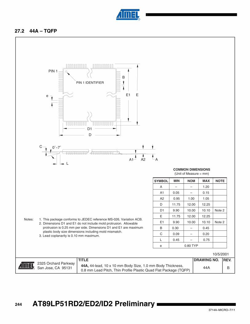
27.2 44A – TQFP
2325 Orchard Parkway San Jose, CA 95131
TITLE DRAWING NO.
R
REV.
44A, 44-lead, 10 x 10 mm Body Size, 1.0 mm Body Thickness,0.8 mm Lead Pitch, Thin Profile Plastic Quad Flat Package (TQFP)
B44A
10/5/2001
PIN 1 IDENTIFIER
0˚~7˚
PIN 1
L
C
A1 A2 A
D1
D
e E1 E
B
COMMON DIMENSIONS(Unit of Measure = mm)
SYMBOL MIN NOM MAX NOTE
Notes: 1. This package conforms to JEDEC reference MS-026, Variation ACB. 2. Dimensions D1 and E1 do not include mold protrusion. Allowable
protrusion is 0.25 mm per side. Dimensions D1 and E1 are maximum plastic body size dimensions including mold mismatch.
3. Lead coplanarity is 0.10 mm maximum.
A – – 1.20
A1 0.05 – 0.15
A2 0.95 1.00 1.05
D 11.75 12.00 12.25
D1 9.90 10.00 10.10 Note 2
E 11.75 12.00 12.25
E1 9.90 10.00 10.10 Note 2
B 0.30 – 0.45
C 0.09 – 0.20
L 0.45 – 0.75
e 0.80 TYP
2443714A–MICRO–7/11
AT89LP51RD2/ED2/ID2 Preliminary

AT89LP51RD2/ED2/ID2 Preliminary
27.3 44J – PLCC
Notes: 1. This package conforms to JEDEC reference MS-018, Variation AC. 2. Dimensions D1 and E1 do not include mold protrusion.
Allowable protrusion is .010"(0.254 mm) per side. Dimension D1and E1 include mold mismatch and are measured at the extremematerial condition at the upper or lower parting line.
3. Lead coplanarity is 0.004" (0.102 mm) maximum.
A 4.191 – 4.572
A1 2.286 – 3.048
A2 0.508 – –
D 17.399 – 17.653
D1 16.510 – 16.662 Note 2
E 17.399 – 17.653
E1 16.510 – 16.662 Note 2
D2/E2 14.986 – 16.002
B 0.660 – 0.813
B1 0.330 – 0.533
e 1.270 TYP
COMMON DIMENSIONS(Unit of Measure = mm)
SYMBOL MIN NOM MAX NOTE
1.14(0.045) X 45˚ PIN NO. 1
IDENTIFIER
1.14(0.045) X 45˚
0.51(0.020)MAX
0.318(0.0125)0.191(0.0075)
A2
45˚ MAX (3X)
A
A1
B1 D2/E2B
e
E1 E
D1
D
44J, 44-lead, Plastic J-leaded Chip Carrier (PLCC) B44J
10/04/01
2325 Orchard Parkway San Jose, CA 95131
TITLE DRAWING NO.
R
REV.
2453714A–MICRO–7/11

27.4 44M1 – VQFN/MLF
TITLE DRAWING NO.GPC REV. Package Drawing Contact: [email protected] 44M1ZWS H
44M1, 44-pad, 7 x 7 x 1.0 mm Body, Lead Pitch 0.50 mm, 5.20 mm Exposed Pad, Thermally Enhanced Plastic Very Thin Quad Flat No Lead Package (VQFN)
9/26/08
COMMON DIMENSIONS(Unit of Measure = mm)
SYMBOL MIN NOM MAX NOTE
A 0.80 0.90 1.00
A1 – 0.02 0.05
A3 0.20 REF
b 0.18 0.23 0.30
D
D2 5.00 5.20 5.40
6.90 7.00 7.10
6.90 7.00 7.10
E
E2 5.00 5.20 5.40
e 0.50 BSC
L 0.59 0.64 0.69
K 0.20 0.26 0.41Note: JEDEC Standard MO-220, Fig. 1 (SAW Singulation) VKKD-3.
TOP VIEW
SIDE VIEW
BOTTOM VIEW
D
E
Marked Pin# 1 ID
E2
D2
b e
Pin #1 CornerL
A1
A3
A
SEATING PLANE
Pin #1 Triangle
Pin #1 Chamfer(C 0.30)
Option A
Option B
Pin #1 Notch(0.20 R)
Option C
K
K
123
2463714A–MICRO–7/11
AT89LP51RD2/ED2/ID2 Preliminary

AT89LP51RD2/ED2/ID2 Preliminary
27.5 40P6 – PDIP
2325 Orchard Parkway San Jose, CA 95131
TITLE DRAWING NO.
R
REV. 40P6, 40-lead (0.600"/15.24 mm Wide) Plastic Dual Inline Package (PDIP) B40P6
09/28/01
PIN1
E1
A1
B
REF
E
B1
C
L
SEATING PLANE
A
0º ~ 15º
D
e
eB
COMMON DIMENSIONS(Unit of Measure = mm)
SYMBOL MIN NOM MAX NOTE
A – – 4.826
A1 0.381 – –
D 52.070 – 52.578 Note 2
E 15.240 – 15.875
E1 13.462 – 13.970 Note 2
B 0.356 – 0.559
B1 1.041 – 1.651
L 3.048 – 3.556
C 0.203 – 0.381
eB 15.494 – 17.526
e 2.540 TYP
Notes: 1. This package conforms to JEDEC reference MS-011, Variation AC. 2. Dimensions D and E1 do not include mold Flash or Protrusion.
Mold Flash or Protrusion shall not exceed 0.25 mm (0.010").
2473714A–MICRO–7/11

28. Revision History
Revision No. History
Revision A – July 2011 • Initial Release
2483714A–MICRO–7/11
AT89LP51RD2/ED2/ID2 Preliminary

AT89LP51RD2/ED2/ID2 Preliminary
Table of Contents
Features ..................................................................................................... 1
1 Pin Configurations ................................................................................... 2
1.1 44-lead VQFP ....................................................................................................2
1.2 44-lead PLCC ....................................................................................................2
.................................................................................................................... 3
1.3 44-pad VQFN/QFN/MLF ....................................................................................3
1.4 40-pin PDIP .......................................................................................................3
1.5 Pin Description ..................................................................................................4
2 Overview ................................................................................................... 6
2.1 Block Diagram ...................................................................................................8
2.2 System Configuration ........................................................................................8
2.3 Comparison to the Atmel AT89C51RD2/ED2/ID2 ...........................................10
3 Memory Organization ............................................................................ 13
3.1 Program Memory .............................................................................................13
3.2 Internal Data Memory ......................................................................................16
3.3 External Data Memory .....................................................................................17
3.4 Extra RAM (EDATA) ........................................................................................22
3.5 EEPROM .........................................................................................................22
3.6 Extended Stack ...............................................................................................26
4 Special Function Registers ................................................................... 27
5 Enhanced CPU ....................................................................................... 33
5.1 Fast Mode ........................................................................................................33
5.2 Compatibility Mode ..........................................................................................34
5.3 Multiply–Accumulate Unit (MAC) .....................................................................34
5.4 Enhanced Dual Data Pointers .........................................................................37
5.5 Instruction Set Extensions ...............................................................................41
6 System Clock ......................................................................................... 43
6.1 Crystal Oscillator A ..........................................................................................44
6.2 External Clock Source A ..................................................................................45
6.3 Internal RC Oscillator ......................................................................................45
6.4 Crystal Oscillator B (AT89LP51ID2) ................................................................45
6.5 External Clock Source B (AT89LP51ID2) ........................................................46
i3714A–MICRO–7/11
Table of Contents (Continued)6.6 Dual Oscillator Support (AT89LP51ID2) ..........................................................46
6.7 X1/X2 Feature .................................................................................................48
6.8 System Clock Prescaler ..................................................................................49
6.9 Peripheral Clocks ............................................................................................50
6.10 Timer Subclock (AT89L51ID2) ........................................................................52
7 Reset ....................................................................................................... 53
7.1 Power-on Reset ...............................................................................................53
7.2 Brown-out Reset ..............................................................................................54
7.3 External Reset .................................................................................................55
7.4 Hardware Watchdog Reset .............................................................................56
7.5 PCA Watchdog Reset ......................................................................................56
7.6 Software Reset ................................................................................................56
8 Power Saving Modes ............................................................................. 57
8.1 Idle Mode .........................................................................................................57
8.2 Power-down Mode ...........................................................................................58
8.3 Reducing Power Consumption ........................................................................59
8.4 Low Power Configuration ................................................................................60
9 Interrupts ................................................................................................ 61
9.1 Interrupt Priority ...............................................................................................61
9.2 Interrupt Response ..........................................................................................63
9.3 Interrupt Registers ...........................................................................................65
10 External Interrupts ................................................................................. 68
11 Keyboard Interface and General-purpose Interrupts .......................... 68
11.1 Registers .........................................................................................................70
12 I/O Ports .................................................................................................. 71
12.1 Port Configuration ............................................................................................71
12.2 Port Analog Functions .....................................................................................74
12.3 Port Read-Modify-Write ...................................................................................75
12.4 Port Alternate Functions ..................................................................................75
13 Enhanced Timer 0 and Timer 1 with PWM ........................................... 79
13.1 Registers .........................................................................................................80
13.2 Mode 0 – Variable Width Timer/Counter .........................................................82
ii3714A–MICRO–7/11
AT89LP51RD2/ED2/ID2 Preliminary

AT89LP51RD2/ED2/ID2 Preliminary
Table of Contents (Continued)13.3 Mode 1 – 16-bit Auto-Reload Timer/Counter ...................................................83
13.4 Mode 2 – 8-bit Auto-Reload Timer/Counter .....................................................84
13.5 Mode 3 – 8-bit Split Timer ...............................................................................84
13.6 Pulse Width Modulation ...................................................................................85
14 Timer 2 .................................................................................................... 89
14.1 Timer 2 Registers ............................................................................................91
14.2 Capture Mode ..................................................................................................92
14.3 Auto-Reload Mode ...........................................................................................93
14.4 Baud Rate Generator ......................................................................................95
14.5 Frequency Generator (Programmable Clock Out) ...........................................96
15 Programmable Counter Array (PCA) .................................................... 97
15.1 PCA Timer/Counter .........................................................................................97
15.2 PCA Modules .................................................................................................100
15.3 PCA Capture Mode .......................................................................................103
15.4 16-bit Software Timer/ Compare Mode .........................................................103
15.5 High Speed Output Mode ..............................................................................104
15.6 Pulse Width Modulator Mode ........................................................................105
15.7 PCA Watchdog Timer ....................................................................................106
16 Hardware Watchdog Timer ................................................................. 106
16.1 Software Reset ..............................................................................................107
16.2 WDT Registers ..............................................................................................108
17 Serial Interface (UART) ........................................................................ 109
17.1 Multiprocessor Communications ...................................................................111
17.2 Baud Rates ....................................................................................................111
17.3 Framing Error Detection ................................................................................116
17.4 Automatic Address Recognition ....................................................................116
17.5 More About Mode 0 .......................................................................................118
17.6 More About Mode 1 .......................................................................................122
17.7 More About Modes 2 and 3 ...........................................................................124
18 Enhanced Serial Peripheral Interface ................................................ 127
18.1 Interface Description ......................................................................................128
18.2 Master Operation ...........................................................................................131
18.3 Slave Operation .............................................................................................131
iii3714A–MICRO–7/11

Table of Contents (Continued)18.4 Error Conditions .............................................................................................132
18.5 Serial Clock Timing ........................................................................................133
18.6 Registers .......................................................................................................134
19 Two-Wire Serial Interface .................................................................... 136
19.1 Data Transfer and Frame Format ..................................................................137
19.2 Multi-master Bus Systems, Arbitration and Synchronization .........................139
19.3 Overview of the TWI Module .........................................................................141
19.4 Register Overview .........................................................................................143
19.5 Using the TWI ................................................................................................144
19.6 Transmission Modes .....................................................................................146
20 Dual Analog Comparators ................................................................... 159
20.1 Analog Input Muxes .......................................................................................160
20.2 Internal Reference Voltage ............................................................................161
20.3 Comparator Interrupt Debouncing .................................................................161
21 Digital-to-Analog/Analog-to-Digital Converter .................................. 166
21.1 ADC Operation ..............................................................................................168
21.2 Temperature Sensor ......................................................................................169
21.3 DAC Operation ..............................................................................................169
21.4 Clock Selection ..............................................................................................170
21.5 Starting a Conversion ....................................................................................171
21.6 Noise Considerations ....................................................................................171
21.7 Registers .......................................................................................................172
22 Instruction Set Summary .................................................................... 175
22.1 Instruction Set Extensions .............................................................................179
23 On-Chip Debug System ....................................................................... 185
23.1 Physical Interface ..........................................................................................185
23.2 Software Breakpoints ....................................................................................186
23.3 Limitations of On-Chip Debug .......................................................................186
24 Flash Memory Programming .............................................................. 187
24.1 Memory Organization ....................................................................................188
24.2 User Configuration Fuses ..............................................................................190
24.3 Flash Hardware Security ...............................................................................191
24.4 In-Application Programming (IAP) .................................................................192
iv3714A–MICRO–7/11
AT89LP51RD2/ED2/ID2 Preliminary
AT89LP51RD2/ED2/ID2 Preliminary
Table of Contents (Continued)24.5 Bootloader .....................................................................................................200
24.6 In-System Programming (ISP) .......................................................................215
25 Electrical Characteristics .................................................................... 225
25.1 Absolute Maximum Ratings* .........................................................................225
25.2 DC Characteristics .........................................................................................225
25.3 Typical Characteristics ..................................................................................226
25.4 Clock Characteristics .....................................................................................228
25.5 Reset Characteristics ....................................................................................229
25.6 External Memory Characteristics ...................................................................229
25.7 Serial Peripheral Interface Timing .................................................................231
25.8 Two-wire Serial Interface Characteristics ......................................................234
25.9 Serial Port Timing: Shift Register Mode ........................................................235
25.10 Dual Analog Comparator Characteristics ......................................................236
25.11 DADC Characteristics ....................................................................................236
25.12 Test Conditions ..............................................................................................238
26 Ordering Information ........................................................................... 241
26.1 Green Package Option (Pb/Halide-free) ........................................................241
27 Packaging Information ........................................................................ 242
27.1 44AA – VQFP/LQFP ......................................................................................242
27.2 44A – TQFP ...................................................................................................243
27.3 44J – PLCC ...................................................................................................244
27.4 44M1 – VQFN/MLF .......................................................................................245
27.5 40P6 – PDIP ..................................................................................................246
28 Revision History ................................................................................... 247
Table of Contents....................................................................................... i
v3714A–MICRO–7/11

3714A–MICRO–7/11
Atmel Corporation2325 Orchard ParkwaySan Jose, CA 95131USATel: (+1) (408) 441-0311Fax: (+1) (408) [email protected]
Atmel Asia LimitedUnit 1-5 & 16, 19/FBEA Tower, Millennium City 5418 Kwun Tong RoadKwun Tong, KowloonHONG KONGTel: (+852) 2245-6100Fax: (+852) 2722-1369
Atmel Munich GmbHBusiness CampusParkring 4BP 309D-85748 Garching b. MunichGERMANYTel: (+49) 89-31970-0Fax: (+49) 89-3194621
Atmel Japan9F, Tonetsu Shinkawa Bldg.1-24-8 ShinkawaChuo-ku, Tokyo 104-0033JAPANTel: (+81) (3) 3523-3551Fax: (+81) (3) 3523-7581
Disclaimer: The information in this document is provided in connection with Atmel products. No license, express or implied, by estoppel or otherwise, to anyintellectual property right is granted by this document or in connection with the sale of Atmel products. EXCEPT AS SET FORTH IN ATMEL’S TERMS AND CONDI-TIONS OF SALE LOCATED ON ATMEL’S WEB SITE, ATMEL ASSUMES NO LIABILITY WHATSOEVER AND DISCLAIMS ANY EXPRESS, IMPLIED OR STATUTORYWARRANTY RELATING TO ITS PRODUCTS INCLUDING, BUT NOT LIMITED TO, THE IMPLIED WARRANTY OF MERCHANTABILITY, FITNESS FOR A PARTICULARPURPOSE, OR NON-INFRINGEMENT. IN NO EVENT SHALL ATMEL BE LIABLE FOR ANY DIRECT, INDIRECT, CONSEQUENTIAL, PUNITIVE, SPECIAL OR INCIDEN-TAL DAMAGES (INCLUDING, WITHOUT LIMITATION, DAMAGES FOR LOSS OF PROFITS, BUSINESS INTERRUPTION, OR LOSS OF INFORMATION) ARISING OUTOF THE USE OR INABILITY TO USE THIS DOCUMENT, EVEN IF ATMEL HAS BEEN ADVISED OF THE POSSIBILITY OF SUCH DAMAGES. Atmel makes norepresentations or warranties with respect to the accuracy or completeness of the contents of this document and reserves the right to make changes to specificationsand product descriptions at any time without notice. Atmel does not make any commitment to update the information contained herein. Unless specifically providedotherwise, Atmel products are not suitable for, and shall not be used in, automotive applications. Atmel’s products are not intended, authorized, or warranted for useas components in applications intended to support or sustain life.
© 2011 Atmel Corporation. All rights reserved.
Atmel®, Atmel logo and combinations thereof, and others are registered trademarks or trademarks of Atmel Corporation or its subsidiaries. Otherterms and product names may be trademarks of others.