662 ieee transactions on circuits and …eprints.qut.edu.au/37477/1/ghosh2.pdf662 ieee transactions...
TRANSCRIPT
662 IEEE TRANSACTIONS ON CIRCUITS AND SYSTEMS—I: REGULAR PAPERS, VOL. 53, NO. 3, MARCH 2006
Frequency-Domain Characterization of SlidingMode Control of an Inverter Used in
DSTATCOM ApplicationRajesh Gupta, Student Member, IEEE, and Arindam Ghosh, Fellow, IEEE
Abstract—In this paper, the commonly used switching schemesfor sliding mode control of power converters is analyzed anddesigned in the frequency domain. Particular application of adistribution static compensator (DSTATCOM) in voltage controlmode is investigated in a power distribution system. Tsypkin’smethod and describing function is used to obtain the switchingconditions for the two-level and three-level voltage source in-verters. Magnitude conditions of carrier signals are developedfor robust switching of the inverter under carrier-based modu-lation scheme of sliding mode control. The existence of bordercollision bifurcation is identified to avoid the complex switchingstates of the inverter. The load bus voltage of an unbalancedthree-phase nonstiff radial distribution system is controlled usingthe proposed carrier-based design. The results are validated usingPSCAD/EMTDC simulation studies and through a scaled labo-ratory model of DSTATCOM that is developed for experimentalverification.
Index Terms—Bifurcation, distribution static compensator(DSTATCOM), forced-switching, sliding mode, Tsypkin’s locus.
I. INTRODUCTION
ANALYSIS of sliding mode control in the frequency domainhas been of recent interest for the characterization of
limit cycle with relay controller [1]–[3]. Limitation of thedescribing function is well understood, and Tsypkin’s methodneeds to be replaced for more accurate results [2]–[4]. Forpower converters, the relay output is the pulsewidth-modulated(PWM) input to the switching element of the inverter and, forhigh-power applications, the switching loss increases linearlywith the switching frequency. Therefore, the switching deviceneeds to switch at low frequency. As opposed to the signumfunction used in the ideal sliding mode, a hysteresis band needsto be introduced in two-level switching in order to limit theswitching frequency of converters. However, at low switchingfrequency, low attenuation of the system leads to the highmagnitude of switching harmonics. There have been a fewproposals for the calculation of the switching frequency forsimple circuits [5]. However, trial and error procedure are usually
Manuscript received November 4, 2004; revised April 28, 2005 and June 30,2005. This work was supported in part by the Central Power Research Insti-tute, Bangalore, India through the project “Development of Active Power LineConditioners for Power Distribution Systems.” This paper was recommendedby Associate Editor M. K. Kazimierczuk.
The authors are with the Department of Electrical Engineering, IndianInstitute of Technology, Kanpur 208016, India (e-mail: [email protected];[email protected]).
Digital Object Identifier 10.1109/TCSI.2005.859053
employed to arrive at the correct switching frequency for higherorder circuits [6]. In order to reduce the switching losses andswitching harmonics, a few configuration of three-level invertershave been proposed [7], [8]. However, both the two-level andthree-level inverters lead to the variable switching frequencyover one fundamental cycle of power frequency. The switchingcondition also varies with the variation of parameters [9],[10]. Carrier-based modulation is used to achieve constantswitching frequency [5], [7], [9]–[11] at the expense of a smallsacrifice in transient and steady-state characteristics. Magnitudeof the carrier is an important design parameter, and there isa minimum magnitude below which the synchronism is lost.Both the steady-state and transient performances deterioratewith the increase in the magnitude of the carrier.
In this paper, sliding mode control for a distribution staticcompensator (DSTATCOM) is designed for a power distributionsystem.Commonlyusedswitchingschemesforpowerconvertersof sliding mode, e.g., two-level, three-level, variable hysteresis,and carrier-based modulation, are analyzed and designed inthe frequency domain. Tsypkin’s locus of linear system anddescribing function of nonlinear relay [12], [13] are used todetermine the stable switching of power converters. Analyticaland graphical procedures are used for the characterization ofswitching frequency for the two- and three-level inverters.Further, the variable switching conditions are analyzed, and aprocedure to maintain constant maximum switching frequency issuggested. A switching algorithm for the three-level inverteris used with a small dead zone. Commonly used carriersfor the forced switching of inverters are also dealt with inthe frequency domain. Sinusoidal signal is introduced as thefundamental carrier signal for the carrier-based modulationof sliding mode control. Minimum magnitude conditions ofdifferent carriers are determined for fixed frequency switching.Below this, the synchronism is lost. For robust switching atprefixed frequency, the concept of parameter sensitivity isintroduced. The load bus voltage of a three-phase nonstiffradial distribution system is controlled using sliding modecontrol of DSTATCOM. Conditions of unbalancing, uncertainty,and parameter variations are considered for robust switchingof inverter using carrier-based modulation. Border collisionbifurcation is identified for the carrier-based modulation, andit is shown that the hysteresis band and carrier magnitudemust be chosen carefully to avoid chattering and harmonicswitching, respectively. An experimental verification of theswitching schemes developed in this paper is provided usingscaled laboratory model of a single-phase DSTATCOM.
1057-7122/$20.00 © 2006 IEEE
GUPTA AND GHOSH: FREQUENCY-DOMAIN CHARACTERIZATION OF SLIDING MODE CONTROL USED IN DSTATCOM APPLICATION 663
II. SLIDING MODE CONTROL OF DSTATCOM
A. DSTATCOM Model
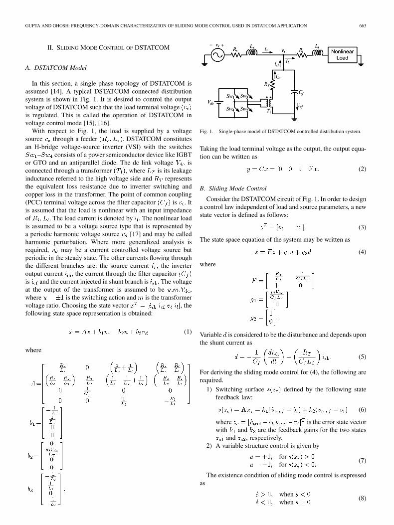
In this section, a single-phase topology of DSTATCOM isassumed [14]. A typical DSTATCOM connected distributionsystem is shown in Fig. 1. It is desired to control the outputvoltage of DSTATCOM such that the load terminal voltageis regulated. This is called the operation of DSTATCOM involtage control mode [15], [16].
With respect to Fig. 1, the load is supplied by a voltagesource through a feeder . DSTATCOM constitutesan H-bridge voltage-source inverter (VSI) with the switches
– consists of a power semiconductor device like IGBTor GTO and an antiparallel diode. The dc link voltage isconnected through a transformer , where is its leakageinductance referred to the high voltage side and representsthe equivalent loss resistance due to inverter switching andcopper loss in the transformer. The point of common coupling(PCC) terminal voltage across the filter capacitor is . Itis assumed that the load is nonlinear with an input impedanceof , . The load current is denoted by . The nonlinear loadis assumed to be a voltage source type that is represented bya periodic harmonic voltage source [17] and may be calledharmonic perturbation. Where more generalized analysis isrequired, may be a current controlled voltage source butperiodic in the steady state. The other currents flowing throughthe different branches are: the source current , the inverteroutput current , the current through the filter capacitoris and the current injected in shunt branch is . The voltageat the output of the transformer is assumed to be ,where is the switching action and is the transformervoltage ratio. Choosing the state vector , thefollowing state space representation is obtained:
(1)
where
Fig. 1. Single-phase model of DSTATCOM controlled distribution system.
Taking the load terminal voltage as the output, the output equa-tion can be written as
(2)
B. Sliding Mode Control
Consider the DSTATCOM circuit of Fig. 1. In order to designa control law independent of load and source parameters, a newstate vector is defined as follows:
(3)
The state space equation of the system may be written as
(4)
where
Variable is considered to be the disturbance and depends uponthe shunt current as
(5)
For deriving the sliding mode control for (4), the following arerequired.
1) Switching surface defined by the following statefeedback law:
(6)
where is the error state vectorwith and are the feedback gains for the two states
and , respectively.2) A variable structure control is given by
forfor
(7)
The existence condition of sliding mode control is expressedas
whenwhen
(8)
664 IEEE TRANSACTIONS ON CIRCUITS AND SYSTEMS—I: REGULAR PAPERS, VOL. 53, NO. 3, MARCH 2006
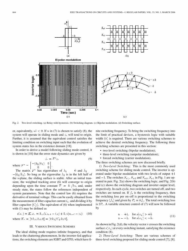
Fig. 2. Two-level switching. (a) Relay with hysteresis. (b) Switching diagram. (c) Bipolar modulation. (d) Switching surface.
or, equivalently, . If in (7) is chosen to satisfy (8), thesystem will operate in sliding mode and will tend to origin.Further, it is assumed that the equivalent control satisfies thelimiting condition on switching input such that the evolution ofsystem states lies in the existence domain [18].
In order to derive a model following sliding mode control, itis shown in [18] that the error state dynamics are given by
(9)
where .
The matrix has eigenvalues of and. So long as the eigenvalue is in the left half of
the s-plane, the sliding surface is stable. After an initial tran-sient, the weighted tracking error (6) will converge to origindepending upon the time constant , and, understeady state, the states follow the references independent ofsystem parameters. Note that the control law (6) requires thederivative of terminal voltage. This can be easily obtained fromthe measurement of filter capacitor current and dividing it byfilter capacitor . The equivalent of (6) when implementedwith (1) may be defined as
(10)
where .
III. VARIOUS SWITCHING SCHEMES
The ideal sliding mode requires infinite frequency, and thatleads to the chattering phenomenon. In the inverter-fed applica-tions, the switching elements are IGBT and GTO, which have fi-
nite switching frequency. To bring the switching frequency intothe limit of practical devices, a hysteresis logic with suitablewidth is required. There are various switching schemes toachieve the desired switching frequency. The following threeswitching schemes are presented in this section:
• two-level switching (bipolar modulation);• three-level switching (unipolar modulation);• forced switching (carrier modulation).
The three switching schemes are now discussed briefly.1) Two-Level Switching: This is the most commonly used
switching scheme for sliding mode control. The inverter is op-erated under bipolar modulation with two levels of output 1and 1. The switches , and , in Fig. 1 are op-erated in pair. Fig. 2(a) shows the switching logic, and Fig. 2(b)and (c) shows the switching diagram and inverter output level,respectively. In each cycle, two switches are turned off, and twoswitches are turned on. If is the switching frequency, thenthe switching loss per on–off is proportional to the switchingfrequency and given by . The total switching lossis . A variable structure control of (7) will now be followedby
forfor
(11)
As shown in Fig. 2(d), the velocity vector crosses the switchingsurface at every switching instant, satisfying the existencecondition (8).
2) Three-Level Switching: There are various schemes ofthree-level switching proposed for sliding mode control [7], [8].

GUPTA AND GHOSH: FREQUENCY-DOMAIN CHARACTERIZATION OF SLIDING MODE CONTROL USED IN DSTATCOM APPLICATION 665
Fig. 3. Three-level switching. (a) Relay with hysteresis and dead zone. (b) Switching diagram. (c) Unipolar modulation. (d) Switching surface.
The scheme presented in this paper is based on the followingvariable structure control algorithm and shown in Fig. 3(a).
If then
forfor
(12)
else if then
forfor
It is assumed that the variable structure control (12) satisfies theexistence condition of the sliding mode control (8) for switchingsurface shifted by a factor and fromits value for the condition of and ,respectively, in (12). This scheme leads to unipolar modulation,and the inverter has three levels of output, i.e., 1, 0, and 1,as shown in Fig. 3(c). In this scheme, the left leg is kept atlow switching frequency, thus accordingly lowering the oper-ational cost. Fig. 3(b) shows the pair of switches andthat change their status at every half cycle of switching functionat power frequency as the switching function is never al-lowed to touch the surface , and reverses its polaritywith every half cycle of switching function as shown in Fig. 3(d).A suitably small value of dead zone is introduced to avoid
any bipolar modulation while approaches zero. The pos-sibility of bipolar modulation is there due to the finite samplingmeasurement. This is because, in between the two samplinginstants, the switching function might cross the surface
and the switching algorithm (12) of opposite polaritywill follow. However, the increase in the dead zone increases thesteady-state tracking error. Therefore, the dead zone shouldbe chosen as a minimum to just avoid any crossing of .The right leg comprising switches and is kept at highswitching frequency similar to the two-level scheme. Althoughthe switching frequency as seen by the system is the same, theswitching losses are reduced to approximately half, i.e., plusa small amount due to a low-frequency switching leg. Moreover,due to the reduction of pulse height of the inverter output to half,the ripple in the system output is also reduced to half.
Both conditions (11) and (12) lead to the quasi-slidingregime. The two switching schemes presented above possessan excellent robust tracking that is insensitive to parameterchanges. However, both schemes suffer from the disadvantageof variable switching frequency. To overcome this disadvantage,there are two methods prevailing in the practice: carrier-basedmodulation and variable hysteresis band. The first methodis discussed below while the second method is presented inSection IV-B.
3) Forced Switching: Prefixed switching frequency can beobtained by comparing the switching function with fixed fre-quency carrier signal. Fig. 4(b) shows the block diagram fortwo-level forced switching using carrier and hysteresis band
. The carrier signal may be either a sinusoidal, triangular, or

666 IEEE TRANSACTIONS ON CIRCUITS AND SYSTEMS—I: REGULAR PAPERS, VOL. 53, NO. 3, MARCH 2006
Fig. 4. Carrier-based modulation. (a) Switching function modulation. (b) Block diagram.
three-level disturbance signal. In this method, the sliding modecontroller changes the control input at the crossing of the carrierand is delayed by hysteresis band , as shown in Fig. 4(a). Thetechnique retains the robustness properties of hysteresis con-troller while achieving the constant switching frequency. Thereis, however, a small tracking error depending upon the type andmagnitude of carrier signal. Further, there is a minimum mag-nitude of different carriers at different frequencies to lock theinverter at a fixed carrier frequency. The inverter may enter intocomplex switching states below this magnitude. Moreover, thetracking error and settling time increase with the increase in themagnitude of the carrier. Therefore, it is essential to use the cor-rect carrier with optimal magnitude.
IV. FREQUENCY-DOMAIN CHARACTERIZATION
In the sliding mode control of power converters, the relayoutput is implemented as the PWM input to the plant. Thisis the normal operating mode of the system. Hysteresis isthe design parameter that is intentionally introduced with therelay to control the switching frequency of the converters,which depends upon the hysteresis band , system parameters,and the feedback gains. Accurate estimation of the switchingfrequency is the important design requirement for the closed-loop control of power converters. In this section, a frequency-domain approach is proposed to estimate the switching frequencyand switching harmonics in the two- and three-level inverteroperation for DSTATCOM. Also, the conditions for constantswitching frequency operation for carrier-based modulation aredetermined. Describing function and Tsypkin’s methods arethe two main tools used to analyze and design the switchingoperations.
Consider the state-space description of the system of Fig. 1as obtained in (1) and (2). Let the switching function asdefined by (10) consist of two parts, i.e., and such that
(13)
(14)
where
(15)
Fig. 5. Sliding-mode-controlled system.
Fig. 5 shows the block diagram of the sliding-mode-controlledsystem of Fig. 1 with one of the switching schemes discussed inSection III.
A. Steady-State Analysis Using Tsypkin’s Method
Both the source voltage and harmonic perturbationdue to the nonlinear load are periodic. Then, for an asymptot-ically stable DSTATCOM converter model (1), let denotethe combined steady-state response of feedback function dueto the source and . Furthermore, in the steady state,can be subtracted from , yielding net reference for theDSTATCOM as follows:
(16)
Let represent the combined steady-state output due to and. Therefore, the block diagram of Fig. 5 may be redrawn as
in Fig. 6, thus eliminating the sources and while retainingthe rest of the system.
The describing function method or Tsypkin’s method maybe used with the model of system shown in Fig. 6. In the de-scribing function approach, it is assumed that the input/outputof the nonlinear element is single-frequency sinusoidal input.However, using Tsypkin’s method, a more exact analysis maybe done by assuming that the input/output of the nonlinear el-ement is a periodic signal [12]. Fig. 7 shows the quasi-linearmodel for the steady-state analysis of converter switching. Forsteady-state analysis, the reference is assumed to be zero,and represents the describing function of the relay ele-ment. The remnant harmonics are added as an external signalat the output of relay. Here, represents the integer multipleof the switching frequency and is phase at the th harmonic

GUPTA AND GHOSH: FREQUENCY-DOMAIN CHARACTERIZATION OF SLIDING MODE CONTROL USED IN DSTATCOM APPLICATION 667
Fig. 6. Decoupling of source voltage and harmonic perturbation.
Fig. 7. Quasi-linear model for steady-state analysis.
number. The signals at each point, i.e., , , and , areperiodic and may be represented by Fourier series. For self-os-cillatory response, the external input to the relay is assumed tobe zero, i.e., . The open-loop transfer function ofthe quasi-linear model for the DSTATCOM-controlled systemis obtained from (1) and (10) as
(17)
Expression for transfer function is given in Appendix B.The difference between the number of poles and zeros foris one, and therefore the following will hold:
(18a)
(18b)
In the following, Tsypkin’s locus is used to determine the fre-quency and magnitude of oscillation in the switching function.Consider the two-level relay characteristics of Fig. 2(a) with theoutput level being equal to 1. Using Tsypkin’s formulation,let us define as [12]
(19)
(20)
Note that only the odd harmonics are considered in (19) and (20)since the two-level relay characteristic is skew-symmetric. Thesolution of limit cycle is given by [12]
(21)
(22)
Fig. 8. Tsypkin’s locus and describing function.
Now let us define the harmonic summation in (19) and (20) asfollows:
(23)
(24)
The plot of versus withvarying frequency is defined here as the Tsypkin’s locus.Using (19)-(24), the following equation may be written as:
(25)
(26)
The conditions (25) and (26) can be checked graphically, andthe frequency of self-oscillation that is the same as the switchingfrequency of the inverter may be determined as shown in Fig. 8.Furthermore, the switching frequency determined is stable ifit satisfies the following condition:
(27)
The magnitude of switching harmonics in the terminalvoltage may be calculated from the frequency-domain transferfunction of the model in Fig. 6 at the switching frequencywith (2) as its output equation.
Property 1: For a two-level inverter, the switching conditionsare variable over one fundamental cycle of switching functionat power frequency.
Proof: Let us first assume that the feedback gains in (10)are chosen such that the system has sufficient stability margins.Under this condition, the two-level hysteresis nonlinearity cansafely be approximated by a gain through an incremental-inputdescribing function. Assume that the closed-loop frequencyresponse of the system has small error from its unity gainand zero-phase condition at the power frequency. The error
668 IEEE TRANSACTIONS ON CIRCUITS AND SYSTEMS—I: REGULAR PAPERS, VOL. 53, NO. 3, MARCH 2006
increases for higher order harmonics. Under this condition, theswitching function input to the nonlinearity consists of limitcycle at switching frequency and a small error component atpower frequency carrying higher order harmonics. Since theswitching component is very fast as compared to the low-fre-quency error, the input to the nonlinearity at any time instant isassumed to be a limit cycle with a bias. Let be the amplitudeof the limit cycle and be the constant bias. Then, the signaldual-input describing function is obtained as follows [13]:
(28)
(29)
The magnitude of bias varies between to throughzero along the one cycle of fundamental frequency of theswitching function. Consider the positive bias of input tothe relay of Fig. 2(a). The net input to the relay will now causemore switching duration for 1 level than for 1 level. Let thetwo levels of voltage be in the ratio of : 1. The average outputof the relay is given by .Now for bias the output of relay may be calculated fromincremental input describing function (29) and equated as
(30)
Let us define, and .Then, from (30), we obtain
(31)
Also, from (28), we obtain
(32)
Substituting andinto (32), the following is obtained:
(33)
Inverting (33) yields
(34)
Note from (34) that the imaginary part is independent of andthe expression for switching frequency may be obtained from(22) by replacing by as
(35)
Comparing (35) with (25), it is clear that bias has the ef-fect of increase in effective hysteresis band and hence reductionin switching frequency. Fig. 8 illustrates this phenomenon forfew values of and . Also, note from (34) and (35) that thenegative bias, i.e., has the same effect as positive bias. Theonly difference is that the switch will remain in the 1 level fora longer duration than will the 1 level. Furthermore, the limitcycle magnitude and switching harmonics also increase with theincrease in bias on either side. This is due to a reduction in at-
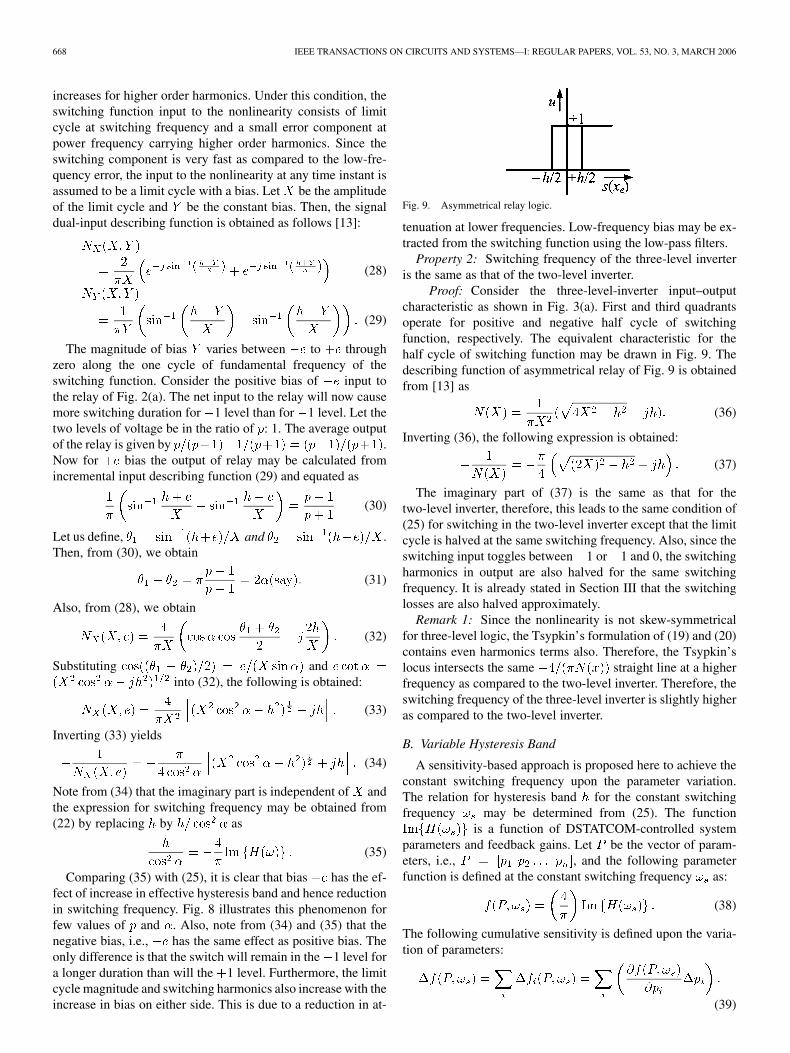
Fig. 9. Asymmetrical relay logic.
tenuation at lower frequencies. Low-frequency bias may be ex-tracted from the switching function using the low-pass filters.
Property 2: Switching frequency of the three-level inverteris the same as that of the two-level inverter.
Proof: Consider the three-level-inverter input–outputcharacteristic as shown in Fig. 3(a). First and third quadrantsoperate for positive and negative half cycle of switchingfunction, respectively. The equivalent characteristic for thehalf cycle of switching function may be drawn in Fig. 9. Thedescribing function of asymmetrical relay of Fig. 9 is obtainedfrom [13] as
(36)
Inverting (36), the following expression is obtained:
(37)
The imaginary part of (37) is the same as that for thetwo-level inverter, therefore, this leads to the same condition of(25) for switching in the two-level inverter except that the limitcycle is halved at the same switching frequency. Also, since theswitching input toggles between 1 or 1 and 0, the switchingharmonics in output are also halved for the same switchingfrequency. It is already stated in Section III that the switchinglosses are also halved approximately.
Remark 1: Since the nonlinearity is not skew-symmetricalfor three-level logic, the Tsypkin’s formulation of (19) and (20)contains even harmonics terms also. Therefore, the Tsypkin’slocus intersects the same straight line at a higherfrequency as compared to the two-level inverter. Therefore, theswitching frequency of the three-level inverter is slightly higheras compared to the two-level inverter.
B. Variable Hysteresis Band
A sensitivity-based approach is proposed here to achieve theconstant switching frequency upon the parameter variation.The relation for hysteresis band for the constant switchingfrequency may be determined from (25). The function
is a function of DSTATCOM-controlled systemparameters and feedback gains. Let be the vector of param-eters, i.e., , and the following parameterfunction is defined at the constant switching frequency as:
(38)
The following cumulative sensitivity is defined upon the varia-tion of parameters:
(39)
GUPTA AND GHOSH: FREQUENCY-DOMAIN CHARACTERIZATION OF SLIDING MODE CONTROL USED IN DSTATCOM APPLICATION 669
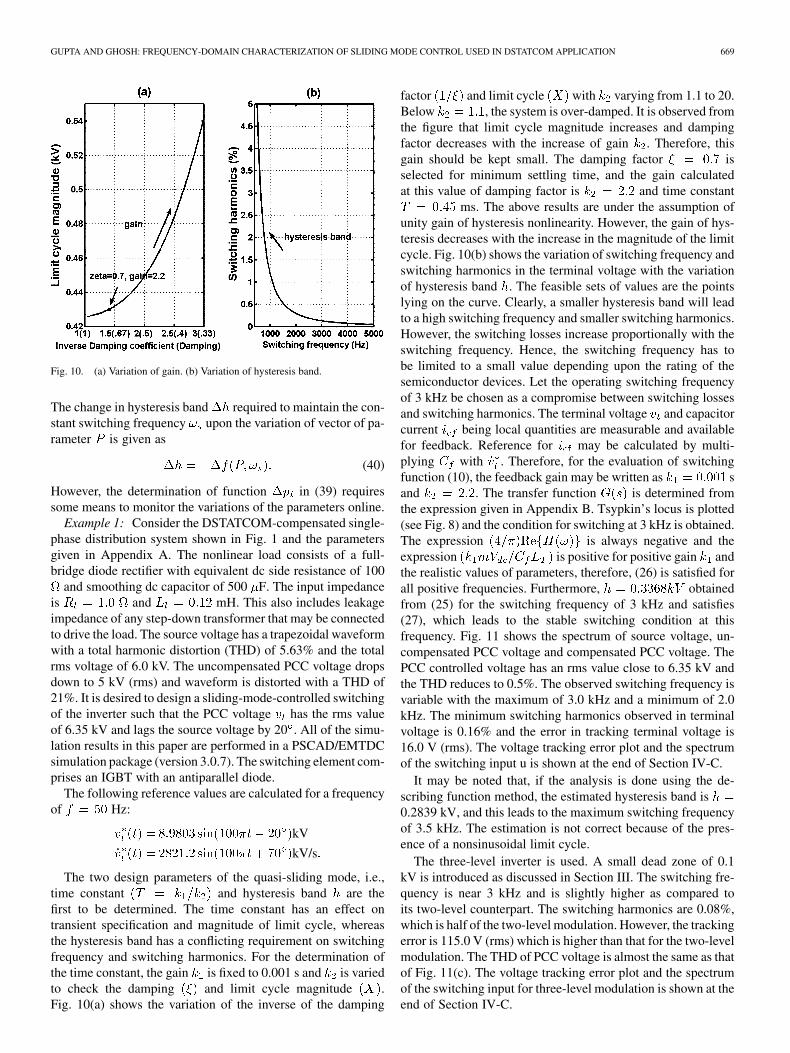
Fig. 10. (a) Variation of gain. (b) Variation of hysteresis band.
The change in hysteresis band required to maintain the con-stant switching frequency upon the variation of vector of pa-rameter is given as
(40)
However, the determination of function in (39) requiressome means to monitor the variations of the parameters online.
Example 1: Consider the DSTATCOM-compensated single-phase distribution system shown in Fig. 1 and the parametersgiven in Appendix A. The nonlinear load consists of a full-bridge diode rectifier with equivalent dc side resistance of 100
and smoothing dc capacitor of 500 F. The input impedanceis and mH. This also includes leakageimpedance of any step-down transformer that may be connectedto drive the load. The source voltage has a trapezoidal waveformwith a total harmonic distortion (THD) of 5.63% and the totalrms voltage of 6.0 kV. The uncompensated PCC voltage dropsdown to 5 kV (rms) and waveform is distorted with a THD of21%. It is desired to design a sliding-mode-controlled switchingof the inverter such that the PCC voltage has the rms valueof 6.35 kV and lags the source voltage by 20 . All of the simu-lation results in this paper are performed in a PSCAD/EMTDCsimulation package (version 3.0.7). The switching element com-prises an IGBT with an antiparallel diode.
The following reference values are calculated for a frequencyof Hz:
kV
kV/s
The two design parameters of the quasi-sliding mode, i.e.,time constant and hysteresis band are thefirst to be determined. The time constant has an effect ontransient specification and magnitude of limit cycle, whereasthe hysteresis band has a conflicting requirement on switchingfrequency and switching harmonics. For the determination ofthe time constant, the gain is fixed to 0.001 s and is variedto check the damping and limit cycle magnitude .Fig. 10(a) shows the variation of the inverse of the damping
factor and limit cycle with varying from 1.1 to 20.Below , the system is over-damped. It is observed fromthe figure that limit cycle magnitude increases and dampingfactor decreases with the increase of gain . Therefore, thisgain should be kept small. The damping factor isselected for minimum settling time, and the gain calculatedat this value of damping factor is and time constant
ms. The above results are under the assumption ofunity gain of hysteresis nonlinearity. However, the gain of hys-teresis decreases with the increase in the magnitude of the limitcycle. Fig. 10(b) shows the variation of switching frequency andswitching harmonics in the terminal voltage with the variationof hysteresis band . The feasible sets of values are the pointslying on the curve. Clearly, a smaller hysteresis band will leadto a high switching frequency and smaller switching harmonics.However, the switching losses increase proportionally with theswitching frequency. Hence, the switching frequency has tobe limited to a small value depending upon the rating of thesemiconductor devices. Let the operating switching frequencyof 3 kHz be chosen as a compromise between switching lossesand switching harmonics. The terminal voltage and capacitorcurrent being local quantities are measurable and availablefor feedback. Reference for may be calculated by multi-plying with . Therefore, for the evaluation of switchingfunction (10), the feedback gain may be written as sand . The transfer function is determined fromthe expression given in Appendix B. Tsypkin’s locus is plotted(see Fig. 8) and the condition for switching at 3 kHz is obtained.The expression is always negative and theexpression is positive for positive gain andthe realistic values of parameters, therefore, (26) is satisfied forall positive frequencies. Furthermore, obtainedfrom (25) for the switching frequency of 3 kHz and satisfies(27), which leads to the stable switching condition at thisfrequency. Fig. 11 shows the spectrum of source voltage, un-compensated PCC voltage and compensated PCC voltage. ThePCC controlled voltage has an rms value close to 6.35 kV andthe THD reduces to 0.5%. The observed switching frequency isvariable with the maximum of 3.0 kHz and a minimum of 2.0kHz. The minimum switching harmonics observed in terminalvoltage is 0.16% and the error in tracking terminal voltage is16.0 V (rms). The voltage tracking error plot and the spectrumof the switching input u is shown at the end of Section IV-C.
It may be noted that, if the analysis is done using the de-scribing function method, the estimated hysteresis band is0.2839 kV, and this leads to the maximum switching frequencyof 3.5 kHz. The estimation is not correct because of the pres-ence of a nonsinusoidal limit cycle.
The three-level inverter is used. A small dead zone of 0.1kV is introduced as discussed in Section III. The switching fre-quency is near 3 kHz and is slightly higher as compared toits two-level counterpart. The switching harmonics are 0.08%,which is half of the two-level modulation. However, the trackingerror is 115.0 V (rms) which is higher than that for the two-levelmodulation. The THD of PCC voltage is almost the same as thatof Fig. 11(c). The voltage tracking error plot and the spectrumof the switching input for three-level modulation is shown at theend of Section IV-C.

670 IEEE TRANSACTIONS ON CIRCUITS AND SYSTEMS—I: REGULAR PAPERS, VOL. 53, NO. 3, MARCH 2006
Fig. 11. Peak magnitude spectrum, base frequency 50 Hz. (a) Source voltage. (b) Uncompensated PCC voltage. (c) Compensated PCC voltage.
To verify the variable hysteresis band algorithm, a slowlyvarying dc link voltage is applied across the transformer. Thevoltage varies between 400–600 V continuously for the two-level modulation scheme. Using a constant hysteresis band of0.3368 kV, the maximum switching frequency varies between2.5–3.5 kHz. In order to obtain a constant switching frequencyusing (40), the sensitivity functionis calculated at the switching frequency of 3 kHz. The variablehysteresis band algorithm of Section IV-B is implemented, anda constant maximum switching frequency of 3 kHz is obtainedwith the hysteresis band varying between 0.269–0.404 kV. Thedc link voltage is fed back continuously for the calculation ofthe change in hysteresis band.
C. Forced Switching
Consider the external periodic carrier signal of frequencyin Fig. 6. It is desired to determine the minimum magnitude
of the carrier that will force the switching of the inverter at theexternal frequency . The input to the relay is given by
(41)
At synchronization, the following conditions are satisfied [12]:
(42)
For sinusoidal carrier signal , thecondition for forced switching at predefined frequency isobtained as
(43)
(44)
The graphical technique to find out the solution for (43)is shown in Fig. 12. The minimum amplitude requiredto produce the forced switching at is the radius of thecircle drawn from the point of at locus, whichjust touches the inverse describing function of two-level relay
, which is a straight line intersecting the imag-inary axis at and parallel to the real axis. For the inputmagnitudes, more than , there is always two solutionsand with phase angles of and , respectively. However,it is shown in [12] that the solution of is stable whereasis unstable. Condition (44) can easily be checked analytically.
Fig. 12. Carrier magnitude determination.
If the external periodic signal is other than sinusoidal, suchas triangular or pulsed, then, for the approximate analysis,the fundamental component of the periodic signal may beconsidered in (43) and (44). Since the magnitude of the higherorder odd-harmonic components of the periodic signal aresignificantly small, they cannot cause the forced harmonicswitching.
Theorem 1: The minimum magnitude of carrier signal re-quired for robust forced switching is given by
(45)Proof: It is assumed that the self-oscillation frequency is
higher than the desired forced external frequency at the chosenhysteresis band . With reference to Fig. 12, is theradius of the circle to which the straight lineis a tangent. Clearly, and . There-fore, the left-hand side (LHS) of (45) will be followed and
. For robust switching,it is desired that the inverter must be synchronized with theexternal input frequency even with the uncertainty orvariation of parameters. As has been shown in Fig. 12, an inputmagnitude greater than will keep the synchronization.Therefore, the positive cumulative sensitivity in

GUPTA AND GHOSH: FREQUENCY-DOMAIN CHARACTERIZATION OF SLIDING MODE CONTROL USED IN DSTATCOM APPLICATION 671
Fig. 13. Switching function modulation.
(39) will not affect the forced oscillation condition. However,if the cumulative sensitivity is negative the choice of iscrucial. Small choice of may just pull down the circle totouch the straight line . Therefore, it is requiredto determine the net change upon the variation of all of theparameters. Furthermore, this summation is compared withzero to avoid any positive cumulative sensitivity.
Remark 2: Note that, in the literature [5], [9], [10], a point ofcaution is mentioned that the amplitude of the carrier should notbe less than the oscillating magnitude of the switching functionand the slope of the control signal should not increase the slopeof the carrier. However, under closed-loop operation, it is diffi-cult to test this condition a priori. The above theorem is usefulto ascertain the condition of constant switching frequency of theinverter.
Property 3: Steady-state error in the switching function in-creases with the increase in the magnitude of the carrier signal.
Proof: The property is proved for more commonly usedtriangular carrier in power-converter applications. Let us ig-nore the oscillating limit cycle component in the switching errorfunction of Fig. 7. As assumed in Property 1, there will bea steady-state error at the power frequency and its harmonics.Therefore, the input to the relay is considered as the compar-ison of the low-frequency signal and the high-frequency carrier.Refer to Fig. 13 where the switching error function is com-pared with an external carrier signal and fed to the relaywith a small hysteresis width. The carrier frequency is consid-ered to be significantly high so that the switching functionis considered to be constant for one switching time period. FromFig. 13, it can be shown that the instantaneous average outputvoltage is proportional to the ratio of control voltageand peak of triangular voltage [19], which is given by
(46)
where is the constant that depends upon the logic levelsand equal to unity for bipolar modulation. The expression
in (46) may be considered as the gain in the feed-for-ward path. The input to the system is the periodic signalwith the fundamental frequency of 50 Hz. From Fig. 6, the si-nusoidal transfer function for switching error functionmay be written as
(47)
Clearly, if the amplitude of the carrier signal increases, thenthe system gain decreases. Since the bandwidth of the
Fig. 14. Variation of tracking error and settling time with carrier magnitude.
system is significantly high as compared to the power fre-quency, the steady-state magnitude in the frequency responseof the switching error function increases with the increase inthe amplitude of the carrier signal at low frequency such as atpower frequency. This also in effect increases the tracking errorin the terminal voltage.
Example 2: Consider the system parameters, nonlinear load,and time constant, as discussed in Example 1. In this example,it is illustrated that the constant switching frequency of 3 kHz isachieved using carrier-based modulation.
Carrier modulation allows the choice of a small hysteresisband. However, a very small hysteresis band should be avoidedas it may lead to multiple crossing of the carrier and, therefore,the chattering. Let us consider 0.1 kV. Using the condition(43), the minimum magnitude of sinusoidal carrier required is0.2368 kV (see Fig. 12) and, for a triangular carrier, this mag-nitude is 0.2921 kV with same the fundamental value as that ofthe sinusoidal carrier. The condition (44) is also required to besatisfied as in Example 1. Since the added term is al-ways negative for point A in Fig. 12, therefore (44) is satisfied.The actual minimum magnitudes observed from simulation are0.245 and 0.317 kV for sinusoidal and triangular carriers, re-spectively. The cause of small error is due to the finite termina-tion of Tsypkin’s locus at the 11th harmonic in the estimationof switching frequency. The voltage tracking error and the spec-trum of the switching input using sinusoidal carrier is shown atthe end of this section. The tracking error is 35 V (rms) and theswitching frequency is exactly 3 kHz. The THD of PCC voltageis further improved to 0.1% than that of Fig.11 (c) due to ab-sence of any low frequency switching as in the case of two-levelmodulation.Fig. 14 shows the variation of the tracking error andsettling time with the magnitude of the carrier. It is clear fromFig. 14 that, with the increase in carrier magnitude, both tran-sient and steady-state characteristic deteriorates. Therefore, onemust determine the minimum magnitude of the carrier to syn-chronize the switching at carrier frequency.
Example 3: In this example, the load bus voltage of the three-phase radial distribution is controlled using the DSTATCOM.The configuration of the DSTATCOM as in [15] is considered
672 IEEE TRANSACTIONS ON CIRCUITS AND SYSTEMS—I: REGULAR PAPERS, VOL. 53, NO. 3, MARCH 2006
where three separate voltage source inverters are supplied froma common dc source. Both feeder and load input impedance areunbalanced with following parameters:
0.1155 H
0.0955 H
6.05 0.2155 H
0.1 0.05 H
1.0 0.12 H
2.0 0.2 H
The supply is also unbalanced with 6.0 kV (rms),8.5 kV (rms), and 5.0 kV (rms). The shape of the sourcevoltage is trapezoidal, as discussed in Example 1. Furthermore,the dc voltage may vary from 500 to 520 V and the measuredvalue of the capacitance of phase a has an error of 5%. Thenonlinear load consists of a three-phase diode rectifier with anequivalent dc side resistance of 30 and smoothing dc capacitorof 500 F. The remainder of the parameters and design spec-ifications are same as in Example 2. Under these conditions,it is desired to control the PCC load bus voltage to balanced6.35 kV (rms) using carrier-based modulation with 3 kHz ofswitching frequency. A sliding mode controller is designed asillustrated in Example 2, however, Theorem 1 is used to deter-mine the minimum magnitude for robust switching. A commonminimum magnitude is determined for all three phases consid-ering the worst possible cumulative sensitivity. The followingsensitivity functions are calculated numerically:
0.6725/kV
0.0044 F
0.009 02/mH
0.000 623
7.54 10 mH
6.89 10 mH
6.014 10
where . The cumulative sensitivity is calcu-lated as
0.6725 0.02 0.0044 3.887
7.54 10 20.0 6.89 10
70.0 6.014 10 1.0
0.0306 kV
Therefore, from Theorem 1
0.345 0.0306 0.1 0.2756 kV
and
0.4178
0.0306 0.1
0.3548 kV
The error due to Tsypkin’s locus is accounted for while cal-culating the new magnitude of carrier. Rounding off the small
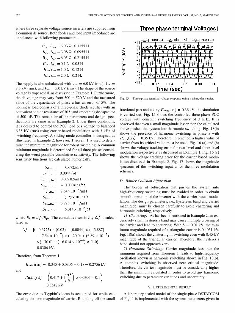
Fig. 15. Three-phase terminal voltage response using a triangular carrier.
fractional part and taking 0.36 kV, the simulationis carried out. Fig. 15 shows the controlled three-phase PCCvoltage with constant switching frequency of 3 kHz. It isobserved that even a small magnitude lesser than the calculatedabove pushes the system into harmonic switching. Fig. 18(b)shows the presence of harmonic switching in phase a with
0.35 kV. Therefore, in practice, a higher value ofcarrier from its critical value must be used. Fig. 16 (a) and (b)shows the voltage-tracking error for two-level and three-levelmodulation respectively as discussed in Example 1. Fig. 16 (c)shows the voltage tracking error for the carrier based modu-lation discussed in Example 2. Fig. 17 shows the magnitudespectrum of the switching input u for the three modulationschemes.
D. Border Collision Bifurcation
The border of bifurcation that pushes the system intohigh-frequency switching must be avoided in order to obtainsmooth operation of the inverter with the carrier-based modu-lation. The design parameters, i.e., hysteresis band and carriermagnitude, must be chosen carefully to avoid chattering andharmonic switching, respectively.
1) Chattering: As has been mentioned in Example 2, an ex-cessively small hysteresis band may cause multiple crossing ofthe carrier and lead to chattering. With 0.01 kV, the min-imum magnitude required of a triangular carrier is 0.4031 kV.Fig. 18(a) shows the chattering in switching even with 0.45-kVmagnitude of the triangular carrier. Therefore, the hysteresisband should not approach zero.
2) Harmonic Switching: Carrier magnitude less than theminimum required from Theorem 1 leads to high-frequencyoscillation known as harmonic switching shown in Fig. 18(b).A complex switching is observed near critical magnitude.Therefore, the carrier magnitude must be considerably higherthan the minimum calculated in order to avoid any harmonicswitching due to parameter variations and uncertainty.
V. EXPERIMENTAL RESULT
A laboratory scaled model of the single-phase DSTATCOMof Fig. 1 is implemented with the system parameters given in

GUPTA AND GHOSH: FREQUENCY-DOMAIN CHARACTERIZATION OF SLIDING MODE CONTROL USED IN DSTATCOM APPLICATION 673
Fig. 16. Voltage tracking error. (a) Two-level, (b) three-level, and (c) carrier-based modulation.
Fig. 17. Magnitude spectrum of switching input, with a base frequency of 50 Hz. (a) Two-level, (b) three-level, and (c) carrier-based modulation.
Fig. 18. Border collision bifurcation. (a) Chattering. (b) Harmonic switching.
Appendix A. However, the voltage levels are reduced as com-pared to kilovolts given in Appendix A. Since the voltage levelsare small, the output of the inverter is directly interfaced tothe PCC through the inductor with the dc link voltage equiv-alent to 125.0 V. The source voltage has the trape-zoidal waveform of the same spectrum as shown in Fig. 11(a)with a magnitude of 60.0 V(rms) The inductance is thesame as that of the equivalent leakage inductance of the trans-former, i.e., 38.5 mH. The nonlinear load connected is a diodebridge rectifier with the parameters the same as those consid-ered in Example 1. The -bridge of the inverter is implementedusing two arms of a Mitsubishi Intelligent Power Module (IPM)PM50CSD120. The sliding mode control and various switchingalgorithm proposed in this paper are implemented using Na-tional Instruments (NI) LabVIEW FPGA module programmingthat runs on reconfigurable I/O NI 7831R embedded in a re-
mote PXI 8186 processor. The terminal voltage and the filtercapacitor current are fed back using the voltage and currenttransducers LEM LV 25-P and LA 55-P, respectively. They arethen fed into the processor through an analog-to-digital (A/D)converter of NI 7831R. The switching logic signals are givento the inverter through the digital output lines of NI 7831Rthat have the TTL compatible voltage levels of 0.0 and 3.3 V.The switching signals provide the gating signal to the IGBTsof IPM through the isolation and dead-time circuit. The dig-ital processor samples the signal at a rate of 15 s. Referencesignals and are generated using the software-basedphase-locked loop implemented using LabVIEW programming.A discrete FIR low-pass filter is connected across the measuredvariables and with a cutoff frequency (1/10) of the sam-pling period to clean up the variables from high-frequency noisesignals.

674 IEEE TRANSACTIONS ON CIRCUITS AND SYSTEMS—I: REGULAR PAPERS, VOL. 53, NO. 3, MARCH 2006
Fig. 19. Two-level modulation. (a) Switching input. (b) Tracking error.
Fig. 20. (a) Source voltage. (b) Controlled voltage.
Fig. 21. Three-level modulation. (a) Gating signal for switch S . (b)Tracking error.
The load bus voltage is controlled using sliding mode controlwith the feedback gains as calculated in Example 1. All ofthe results of previous sections may be scaled by a factor of(1/100). In order to obtain the maximum switching frequencyof 3 kHz with two-level modulation, the calculated value ofhysteresis band 3.368 V is used. The required maximumswitching frequency of around 3 kHz is obtained as shownby the switching signal for the switch in Fig. 19(a). Thesteady-state tracking error in the terminal voltage is shown inFig. 19(b). The tracking error is computed in the processor andis converted into an analog signal through a digital-to-analog(D/A) converter for plotting and shown to the scale of one tenthof the actual value. Fig. 20(a) and (b) shows the waveforms ofthe source voltage and PCC-controlled voltage, respectively,at the reduced scale of 1/50 of the actual values. Similarly, the
Fig. 22. Three-level modulation. Gating signal for (a) switch S and (b)switch S .
Fig. 23. Harmonic switching. (a) Switching input. (b) Tracking error.
three-level modulation is implemented with the same hysteresisband of 3.368 V. However, the minimum dead zonerequired experimentally is 3.0 V to avoid any bipolarmodulation. The high value of dead zone is due to the finitesampling delay of digital processor in the feedback signal.Fig. 21(a) shows the switching signal for the switch andthe steady-state tracking error is shown in Fig. 21(b). Theswitching frequency observed is slightly higher as compared toits two-level counterpart as explained in Remark 1. The switch
also operates at the same frequency with the complemen-tary logic as that for . The left leg switches andoperate at the low frequency as explained in Section III andshown in Fig. 22. The tracking error is significantly high ascompared to the two-level inverter.
Carrier-based modulation is implemented with the sinusoidalcarrier magnitude of 2.368 V and hysteresis band 1.0 Vas calculated in Example 2. Fig. 23 shows the switching inputand tracking error for this magnitude of carrier. The figure il-lustrates the presence of harmonic switching at this minimumvalue of carrier magnitude As discussed in Section IV-D, theharmonic switching gets clear if the carrier magnitude is con-siderably higher than the critical value. Table I is referred inAppendix A. Fig. 24(a) shows the fixed frequency switching at3 kHz and the tracking error in Fig. 24(b) for the sinusoidal car-rier magnitude of 2.8 V. The same result is obtained using thetriangular carrier with the magnitude of 3.5 V having approxi-mately same fundamental value as that of sinusoidal carrier. Thetracking error characteristics for the three modulation schemesare similar to that shown in Fig. 16.

GUPTA AND GHOSH: FREQUENCY-DOMAIN CHARACTERIZATION OF SLIDING MODE CONTROL USED IN DSTATCOM APPLICATION 675
Fig. 24. Carrier-based modulation. (a) Switching input. (b) Tracking error.
TABLE ISYSTEM PARAMETERS
VI. CONCLUSION
Sliding mode control of DSTATCOM improves the totalharmonic distortion and controls the PCC voltage againstthe load nonlinearities and nonideal source. Commonly usedhysteresis-based switching has good dynamic and trackingproperties but suffers from the problem of variable switchingfrequency. Three-level inverter logic yields half of the switchingloss and switching harmonics at the expense of increasedtracking error. Tsypkin’s method together with the describingfunction provides good estimation of the switching frequencyfor power converters. Carrier-based modulation yields robustfixed frequency switching condition with the appropriate designof carrier magnitude. Sinusoidal carrier forms a fundamentalsignal for the design of any carrier-based modulation. Theregion of border collision bifurcation should be identified andthe complex switching states of the inverter, i.e., chatteringand harmonic switching, must be avoided with the properchoice of hysteresis band and carrier magnitude, respectively.Three-phase unbalance load and source parameter have neg-ligible effects on the design of all switching schemes of thesliding mode control. The dc link voltage variation, filter capac-itor, and shunt inductance uncertainty provide a high sensitivityfor the calculation of switching frequency for two-/three-levelmodulation and the determination of carrier magnitude forcarrier-based modulation. Both simulation studies and experi-mental results validate the theory proposed in this paper. Thedesign of any state feedback configuration of DSTATCOMcontrol can be extended using the proposed frequency-domainapproach.
APPENDIX A
The system parameters are given in Table I.
APPENDIX B
Transfer function for a DSTATCOM controlled system de-rived in terms of system parameters and feedback gains is givenas follows:
where
ACKNOWLEDGMENT
The authors would like to thank Prof. A. Joshi of the ElectricalEngineering Department, IIT Kanpur, for providing helpful sug-gestions during the preparation of this manuscript.
REFERENCES
[1] I. Boiko, “Analysis of sliding mode control system in the frequency do-main,” in Proc. Amer. Control Conf., vol. 1, Jun. 4–6, 2003, pp. 186–191.
[2] I. Boiko, L. Fridman, and M. I. Castellanos, “Analysis of second-ordersliding mode algorithms in the frequency domain,” IEEE Trans. Au-tomat. Contr., vol. 49, no. 6, pp. 946–950, Jun. 2004.
[3] S. C. Y. Chung and L. C. Liang, “A transformed Lur’e problem forsliding mode control and chattering reduction,” IEEE Trans. Automat.Contr., vol. 44, no. 3, pp. 563–568, Mar. 1999.
[4] S. Engleberg, “Limitation of describing function for the limit cycle pre-diction,” IEEE Trans. Automat. Contr., vol. 47, no. 11, pp. 1887–1890,Nov. 2002.
[5] D. M. Brod and D. M. Novotny, “Current control of VSI-PWMinverters,” IEEE Trans. Ind. Appl., vol. IA-21, no. 4, pp. 562–570,May/Jun. 1985.
[6] A. Ghosh and G. Ledwich, Power Quality Enhancement Using CustomPower Devices. Boston, MA: Kluwer, 2002.
[7] B. Nicolas, M. Fadel, and Y. Cheron, “Fixed frequency sliding modecontrol of a single phase voltage source inverter with input filter,” inProc. IEEE Int. Symp. Ind. Electron., vol. 1, Jun. 17–20, 1996, pp.470–475.
[8] M. Carpita, P. Farina, and S. Tenconi, “A single phase, sliding modecontrolled inverter with three levels output voltage for UPS or powerconditioning application,” in Proc. 5th Eur. Conf. Power Electron. Ap-plicat., vol. 4, Sep. 13–16, 1993, pp. 272–277.
[9] J. Holtz, “Pulse width modulation for electronic power conversion,”Proc. IEEE, vol. 82, no. 8, pp. 1194–1214, Aug. 1994.
[10] J. F. Silva, Power Electronics Handbook, M. H. Rashid, Ed. New York:Academic, 2001, ch. 19.
[11] B. J. Kang and C. M. Liaw, “Robust hysteresis current-controlled PWMscheme with fixed switching frequency,” Proc. Inst. Elect. Eng. Electr.Power Appl., vol. 47, no. 11, pp. 503–512, Nov. 2001.
[12] D. P. Atherton, Nonlinear Control Engineering. Workingham, U.K.:Van Nostrand, 1975.
[13] A. Gelb and W. E. Vander Veido, Multiple-Input Describing Functionand Nonlinear System Design. New York: McGraw-Hill, 1968.
[14] A. Ghosh and G. Ledwich, “Load compensating DSTATCOM in weakAC systems,” IEEE Trans. Power Del., vol. 18, no. 4, pp. 1302–1309,Oct. 2003.
676 IEEE TRANSACTIONS ON CIRCUITS AND SYSTEMS—I: REGULAR PAPERS, VOL. 53, NO. 3, MARCH 2006
[15] G. Ledwich and A. Ghosh, “A flexible DSTATCOM operating in voltageor current control mode,” Proc. Inst. Elect. Eng. Generation, Trans. Dis-trib., vol. 149, no. 2, pp. 215–224, Mar. 2002.
[16] M. K. Mishra, A. Ghosh, and A. Joshi, “Operation of a DSTATCOMin voltage control mode,” IEEE Trans. Power Del., vol. 18, no. 1, pp.258–264, Jan. 2003.
[17] F. Z. Peng, “Application issues of active power filters,” IEEE Ind. Ap-plicat. Mag., vol. 4, no. 5, pp. 21–30, Sep./Oct. 1998.
[18] M. Carpita and M. Marchesoni, “Experimental study of a power condi-tioning system using sliding mode control,” IEEE Trans. Power Elec-tron., vol. 11, no. 5, pp. 731–742, Sep. 1996.
[19] N. Mohan, T. M. Undeland, and W. P. Robbins, Power Electronics, Con-verters, Applications and Design, Singapore: Wiley, 2003.
Rajesh Gupta (S’05) received the B.E. degree inelectrical engineering from MMM EngineeringCollege, Gorakhpur, India, in 1993 and the M.E.degree from BIT, Mesra, Ranchi, India, in 1995. Heis currently working toward the Ph.D. degree at theIndian Institute of Technology, Kanpur, India.
He is currently on a study leave from the NationalInstitute of Technology, Allahabad, where he isa Senior Lecturer. From 1996 to 1999, he servedas a Lecturer with the Department of Electronicsand Electrical Engineering, G.B Pant Engineering
College, Pauri Garhwal, India. His interests include control of power elec-tronics-based systems, theoretical control ,and systems dynamics.
Arindam Ghosh (S’80–M’83–SM’93–F’06) re-ceived the Ph.D. degree in electrical engineeringfrom the University of Calgary, Calgary, Canada, in1983.
He is a Professor of electrical engineering with theIndian Institute of Technology, Kanpur. He has heldvisiting positions with Nanyang Technological Uni-versity, Singapore, the University of Queensland, andQueensland University of Technology, Australia. Hehas also been a Fulbright Scholar with the Universityof Illinois at Urbana-Champaign and a Distinguished
Visitor with the University of Seville, Seville, Spain. His interests are in controlof power systems and power electronic devices.
Prof. Ghosh is a Fellow of the Indian National Academy of Engineering.