650 data-processing system, 1957 - computer history museum
TRANSCRIPT

-
Customer Engineering
Manual of Instruction
NOTE: This edition, Form 22-6284-1, is written for the Stage 4 IBM
650 Data-Processing System.' This does not obsolete Form 22-6284-0
(Text) and Form 22-6213-1 (Illustrations).
ISSUED T~~ I-p=-_~(fj~A~a:::..-=IJ(~~ BRANCH OFFICE: S ..... ,.,.~ t1w~:4!". DEPARTMENT:
ADDRE~: ____________________________________ ~
Data-Processing System
If this manual is mislaid, please return it to the above address.
© 1956 and 1957 by International Busine$s Machines Corporation 590 Madison Avenue, New York 22, N. Y.
Printed in U. S.A. Form 22-6284-1

SECTION 1. GENERAL PRINCIPLES
General Features _ Nunlber Systems for Digit Representation _________ _ Drum Arrangement and Timings _________________ _ Stored Programming ____________________ --------------------Logical Oq;anizJtion, Data Flow, and Program Control Summary of Various Data Flow Paths _________ _ Physical Organization ____________________ _ Current Requirernents t Dimensions, Weight, and Hcat-
Dissipation Data ______ _ Self -Checking _____________________ _
SECTION II. BASIC PRINCIPLES
PROGRAMMING Storage Address and Operation Codes Summary of Operation Codes _____ _ Examples of Programming _______ _ Loading __________________ _
BASIC ELECTRONIC CIRCUITS Inverters and Double Inverters Cathode Followers ---------------Germanium Crystal Diode Switch and Mix Circuits Diodes Used for Restoration of DC Levels ------VacuuIll Diode Switching Circuits ---------------------Latch Circuits Latch Ring Voltage Am plifiers --------------------------Shaping Amplifiers ____________ -------------------------------------Power Units -------------------Single-Shot Multivibrators ------------------------ ------------------Vacuum Diodes __ -----------------Capacitor Storage _____________ _
GERMANIUM CR YST AL DIODES
PLUGGABLE UNITS ___________ _
BLOCK SYMBOLS Block Symbol Voltage Codes __
TIMING PULSES AND GATES ____________________ _ Basic Recorded Pulses
GLOSSARY OF 650 TIMING DESIGNATIONS ___ _ Tinling Dcsignati:)ns Tinling Designations Special Pulses Timing Gates·
with Abbreviations
PRINCIPLES OF MAGNETIC-DRUM STORAGE _ Drum Ivlechanical Features ____________________ _ Heads for Reading and Writing _______________________________________ _ Reading and Writing Principles ____ _ ______________________ _
MUL TIPLE-WRITE-NO-WRITE CIRCUIT Multiple Write ________________ _ N a-Write Circuit _________________________________ _
SEVEN-TO-FIVE AND FIVE-TO-SEVEN TRANSLATOR CIRCUITS ______________ _ _ _______________________ _ ________________________ _
Seven-to-Five Circuits _ Five-to-Seven Circuits
SELECTED STORAGE SWITCHING
VALIDITY CHECK CIRCUITS Capacitor Storage Validity Check Circuits Buffer Storage Validity Check Circuits
SECTION III. 650 CONSOLE UNIT
PROGRAM CONTROL UNITS __ _____________________________________ _ The Program Register _______________________________________________________ _ Operation and Address Registers _______________________________________ _ Dynamic Selection Circuits _ _ _______________ _
CONTENTS
I-I 1-2 I-3
1-10 1-11 1-16 1-16
1-17 I-17
II-I II-I II-I II-2 II-3
1I-8 II-8 II-9
II-IO II-12 II-14 II-15 II-17 II-18 II-18 II-20 II-22 II-23 II-24
CONTROL CONSOLE KEYS _ Error-Sense Reset Key ___________________________________ _ Error-Reset Key _____ _______________________ _ _____ _ _______________ _ Accumulator Reset Key ____________________________________ _ Program Reset Key __________________________________________ _ Transfer Key Program Start Key Program Stop Key Computer Reset Key
CONTROL CONSOLE LIGHTS Checking Lights _________________________________ _ Operating Lights ______________________ _
CONTROL CONSOLE SWITCHES _________ _ Address Selection Switches __________________________________ _ Control Switch ____ . ________________________________ _ Master Power Off Switch ________________________________________ _ Half-Cycle Swi tch _______________________________________________ _
Programmed Stop Switch Error Stop-Sense Switch ____________________ _ Error Disable Switch _________________________________ _ Overflow Stop-Sense Switch _______________________________________ _ Display Switch ____________________ _ Storage Entry Switches _________________________________________________ _
SECTION IV. ARITHMETIC UNITS
CAPACITOR STORAGE UNITS Distributor Accumulator ___ _
ADDER Bi-Quinary Arithmetic ______________________________________________ _ Adder A and B Entry Switching _____________________________ _ Adder Circuits ________________________________________________________ _
III-7 III-7 III-7 IJI-7 III-7 III-8 III-8 III-8 III-8
III-S III-8 III-8
III-I 2 III-12 III-I 2 III-12 III-13 III-13 III-13 III-I 4 I1I-14 I1I-14 III-I 5
IV-I IV-I IV-J
IV-4 IV-4 IV-6 IV-6
II-25
II-26
II-27 II-27
SECTION V. FUNCTIONS OF OPERATION CODES
II-28 11-28
II-30 II-30 11-31 II-32 II-J J
II-36 II-47 11-48 II-49
II-56 II-56 II-57
II-58 II-58 II-58
II-58
II-59 II-59 II-60
III-I III-I III-2 I1I- 5
10's AND 60's CODES ___________________________________________________ _ Control Commutator ___ _
I HALF CYCLE Restart A _______ _ Restart B ______________________________________ _ Enable Read-In _ . ______________________ _ Start Read-In ______________________ _ Read-In Program Step __________________ _ Circuit Description of the Alternation Control Latches ___ _
D HALF CYCLE 10's AND 60's CODES . _____________________________ _ Code 69 ______________________________________________________________________________ _
ADDITION AND SUBTRACTION OPERATIONS _ Code 10 AU ___________________________________________________________ _ Code 60 Reset and Add Upper _________ _ Code II SU _______________________________________ _ Accumulator Sign Read-Out _________________________________ _ Complement Result Operation __________________________ _
NO OPERATION, STOP AND STORE CODES _______________ _ No Op and Stop Codes 00 and 01 ____________________________________ _ Store Codes (20's) ______________________________ _
SHIFT CODES (30, 31, 35 AND 36) ________ _ _____________________ _ Code 30 SR T ________________________________________________________________ _ Code 3 I SRD ___________________________________________________________________ _ Code 35 SL T _________________________________________ _ Code 36 SCT ___________________________________________________________ _
BRANCH OPERATIONS (40's AND 90's CODES) Code 44 _______________________________________________________________ _ Code 4 5 _______________________________________________________________ _ Code 46 _____________________________________________________________________________ _ Code 47 ______________________________________________ . _____________________________ _ Test Codes (90's) __________________ _
V-I V-I
V-I V-3 V-J V-J V-3 V-J V-3
V-3 V-6
V-9 V-9 V-9
V-II V-II V-12
V-15 V-15 V-18
V-20 V-20 V-21 V-29 V-29
V-31 V-31 V-33 V-35 V-H V-J 5
--'-
--
----
--
CON TEN T S (continued)
MULTIPLICATION (CODE 19) _____________________________________________ _ Functions, Objectives and Circuits ___________________________________ _
DIVISION (CODE 14) __________________________________________________________ _ Principles of Division ___________________________________________________________ _
TABLE LOOKUP ______________________________________________________ _ Table Lookup Check Circuit ___________________________________________ _
SECTION VI. MANUAL OF OPERATION
V-36 V-36
V-42 V-42
V-53 V-57
MANUAL READ-OUT STORAGE OPERATION ________________ VI-I
MANUAL READ-IN STORAGE OPERATION VI-I
SECTION VII. INPUT AND OUTPUT CODES
CONVERSION CIRCUITS FOR READ-JN AND PUNCH OUT _____________________ ____________________________________ _ __________________ _ Read-In from Card (Code 70) _________________________ _ Code 70 __________________________________ -------------------------------------------Code 71-Punch Out to Card ___________________________________________ _
SIGN READ-IN AND PUNCH-OUT ____________________________ _ Sign Read-In ______________________________________________________ --------Word Size Emitter ___________________________________________________________ _
SECTION VIII. ALPHABETIC DEVICE
Alphamerical Input ________________________________________________ _ Alphamerical Output _________________________________________________________ _
SECTION IX. MAIN POWER SUPPLY
INTRODUCTION TO THE ACME SINGLE- AND THREE-PHASE POWER SUPPL Y _________________________________________________ _ Application _______________________________________________________________________ ~ __ Regulator ___________________________________________________________________________ ,_ Metering _____________________________________________________________________________ _ Servicing _____________________________________________________________________________ _
INTERLOCKING ______________________________________________________________________ _ Power-On Interlocking _______________________________________________________ _ Power -Off Sequence ____________________________________________________________ _
VII-I VII-I VU-4 VII-6
VII-II VII-I I VII-I 3
VIII-2 VIII-6
IX-I IX-I IX-I IX-2 IX-3
IX-3 IX-3 IX-3
DC-Off Seq uence _________ _ _____________ _ DC-On Sequence ___________________________ _ Master Power-Off Switch ______________ _
DESCRIPTION AND PURPOSE OF COMPONENTS _______ _ Contactors-Il5 Volts AC ______________________________________________ _ Relays-42 Volts DC _______________________________________________________ _ Timers _________________________________________________________________________________ _
SECTION X. 533 MECHANICAL PRINCIPLES AND CIRCUITS
Punch Drive Mechanism __________ _ Read Drive Mechanism ______________________ _
CONTROL PANEL
533 CIRCUITS
DOUBLE PUNCH. BLANK-COLUMN DETECTION _______ _ Double Punch Detection Circuit _______________________________________ _ Blank Column Detection Circuit _______________________________________ _ Double Punch Detection Exit __________________________________________ _
PUNCH DELAY _______ __________ _ Punch Delay Application _______________ _ Punch Delay Circuit ______________________ _
CONTROL INFORMATION __________ _ Control Information Application ______________________________________ _ Circuit Description ___________________________________________________________ _
READ CODE SELECTOR _______________________________________________________ _ Read Code Selector Application ___ _ __________________________ _ Circuit Description _________________________________ _ RSO (Read Second Only) Wired __________________________________ _
READ FEED CIRCUITS ___ _
PUNCH FEED CIRCUITS ______________________________________________________ _
CARD FEED STOP __________________________________________________________________ _ Circuit Operation
END OF FILE Circuit Operation
PUNCH CODE SELECTOR Punch Code Selector Application _____________________________________ _
CO-SELECTORS ______________________________________________________________________ _
PILOT SELECTORS _______________________________________________________________ _
IX-5 IX-5 IX-5
IX-6 IX-6 IX-6 IX-7
X-I X-3
X-3
X-3
X-3 X-3 X-5 X-5
X-5 X-5 X-5
X-5 X-6 X-6
X-7 X-7 X-7 X-7
X-8
X-8
X-12 X-I2
X-12 X-12
X-12 X-14
X-14
X-14

IBM 650 DATA-PROCESSING SYSTEM

--
SECTION I. GENERAL PRINCIPLES
General Features
The IBM 650 Magnetic-Drum Calculator has been developed to serve an increasing need for dataprocessing equipment to evaluate technical and accounting data. The 650 is completely self-checking without requiring the use of recalculation or special checking programs and consequently provides a high degree of reliability. It has a large memory capacity in the form of magnetic-drum storage and utilizes a system of stored programming that contributes to the ease of an operation and to flexibility in application.
The 650 is available in two models providing an optional main storage capacity for 1000 or 2000 words. A U'ord consists of ten digits and an algebraic sign. Magnetic-drum buffer storage is provided between the main storage and the input and output units for increased speed of operation. Thus, the machine can be calculating while both the input and the output units are operating.
Words are stored serially on the drum. Furthermore, the digits of a word are stored serially within each word interval. Digits are represented by parallel combinations of magnetically stored bits. Information is thus said to be stored serially by word and digit, parallel by bit.
Two systems of digit representation by stored bits are used in the 650. The buffer storages and the arithmetic units use a bi-quinary system, where the presence of two of seven possible parallel stored bits determines the decimal yalue of the digit. All general
storage uses a tu;o-out-of-five bit system, where two of five possible parallel stored bits determine the decimal value of the digit. Each of the word storage positions on the drum is located by a four-digit code or
address. In the stored programming system used by the
650, each instruction (program step) is stored in a drum word-storage location as a ten-digit word.
1-1
When interpreted by the program control circuits, the coded digits of an instruction word give information as to which operation is to be performed, in which storage location to find the data to be used in performing the operation, and in which storage location the next ten-digit instruction word is to be found. A stored sequence of such instruction words forms a program, or progralJ/ routine.
Calculations are performed by electronic means. The calculator can add, subtract, multiply, divide, and make logical tests, such as plus, minus and zero accumulator balance. The program routine can be altered by any of these logical tests or by sensing a control punch in a card. All arithmetical and logical operations are built in and require but little control panel setup. They are activated by the operation code portion of the instruction word.
The calculator will accumulate ten-digit words to develop a twenty-digit total, perform 10-digit X 10-digit multiplication to devc!op a twenty-digit product, and divide a nineteen-digit dividend by a ten-digit divisor to devc!op a ten-digit quotient and a ten-digit remainder. Sign control on all operations is automatic.
Unlike previous IBM calculators, the arithmetic units of the 650 are designed to handle numbers in a serial fashion. Thus, during calculations the ten-digit words are processed by the arithmetic units on a digitby-digit basis with machine time progressing from the units digit through the highest order digit of a word. This is desirable, because information is serially available from storage for presentation to the arithmetic units.
The basic cyclical timings of the 650 are therefore related to digit position rather than digit value as in previous machines. In the 650 the value of a digit is determined by simultaneous combinations of bit pulses on two of the seyen parallel information lines.

I-2 IBM 650
Number Systems for Digit Representation
A recorded magnetic spot is essentially a binary storage device, because it may have either of two magnetic polarities depending on the direction of current flow through the writing head at the time the spot is written. Polarization in one direction is taken to mean a binary 1, while the opposite direction means a binary O. Some system must be used so that a combination of these binary devices can represent the decimal digits 0 through 9.
In the 650 two such systems are used. The two-outof-seven, bi-quinary, system is used for Read Buffer Storage (RBS) and Punch Buffer Storage (PBS) and the arithmetic units. The two-out-of-five system is used for general storage.
Figure I-I shows how the bi-quinary system combines different binary 1 indications from two of seven parallel devices to represent each of the ten decimal digits. In the case of the read and punch buffer storages, the binary devices are recorded magnetic spots on seven parallel tracks. Successive 1 indications from the various combinations of two of the seven tracks during successive digit time intervals will indicate serially the decimal values of the digits of a word. In the case of the arithmetic units the paralleled binary devices are capacitor storage units. Seven parallel capacitors are used to represent each of the ten digits
J---BinClry level I
I Quinary ~vel
Decimol Value onigned to e<lch Binory Type Storage Oevice Digit Value BS BO 04 03 02 01 QO
0 0 I 0 0 0 0 1
I 0 I 0 0 0 1 0
2 0 1 0 0 I 0 0
3 0 , 0 1 0 0 0
4 0 , , 0 0 0 0
S I 0 0 0 0 0 , 6 , 0 0 0 0 , 0
7 , 0 0 0 , 0 0
B , 0 0 1 0 0 0
~ , 0 , 0 0 0 0
fol,a"k -I'" T,at ~ I-- T'o;k ~ Tra;k .1- Tra;k I- T''';k ~ I-- T,.;k ~
Buffer Storage Bond on Drum
Figure 1-1. Bi-Quinary System
of a word. Each row is tested at its digit time by impulses from a drum-driven timing ring. Binary 1 indications from two of the seven capacitors will indicate the decimal value of the digit.
Notice that the bi-quinary system requires that there be a 1 indication from one and only one of the binary indicating devices in each of the two levels. It is this unique characteristic of the bi-quinary system that makes it easily adaptable to self-checking arrangements.
Notice also that the binary level indication determines whether the quinary level indication is to be read as it is or have five added to it to determine the decimal value. This above- or below-five characteristic of the system makes it easily adaptable to calculating circuitry.
Figure 1-2 shows how the two-of-five system combines different binary 1 indications from two-of-five parallel devices to represent each of the ten decimal digits. This system is used only for general storage largely because of the saving of heads and circuits that it affords. This system requires that all information entering general storage passes through a sevento-five conversion matrix and that all information leaving general storage passes through a five-to-seven conversion matrix.
Decimal Value assigned to each Binary Device Digit Value 0 1 2 3 6
0 0 1 - 1 0 0
1 1 1 0 0 0
2 1 0 1 0 0
3 1 0 0 1 0
4 0 1 0 1 0
5 0 0 1 1 0
6 1 0 0 0 1
7 0 1 0 0 1
8 0 0 1 0 1
9 0 0 0 1 1
* Tr~,ck __ Tr~ck_f+Tr~ck .f+Tr~ck "I-Tr~ck ..
1 General Storage Band on Drum
Figure 1-2. Two-Out-of-Five System

SECTION 1. GENERAL PRINCIPLES 1-3
Figure 1-3. Drum Assembly
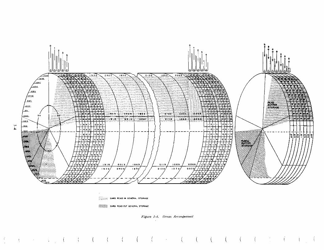
Drum Arrangement and Timings
The calculator is built around the magnetic drum
(Figure 1-3). This drum is a plated metallic cylinder about 4 inches in diameter and 16 inches long. Information is stored on its surface in the form of
magnetic spots. In order to place information on the drum in an orderly fashion and to have the stored
information available periodically, the drum must revolve. In the 650 the drum is driven at a speed of 12,500 rpm. Attached to the end frames and parallel
to the axis of the drum is a number of mounting bars on which are mounted the inductive heads that read
and write the information. Information stored on the drum is erased only by writing new information that
may be read as often as needed without being de
stroyed. The general storage portion of the drum has 2000
addressable locations where ten-digit words can be
stored. Each of these word positions is located by first determining statically which one of the 40 five
track bands it is in across the drum, then dynamically which one of 50 angular drum positions it occupies
around the periphery of the drum.
To accomplish head selection the four-digit address portion of the instruction word is placed in the ad
dress register where it activates the head selection
circuits. Both the static and the dynamic selection are
determined by the numerical value of the four-digit address in the address register.
For static selection purposes the general storage por~ tion of the drum is divided lengthwise into 40 five
track bands, one head per track. Each of the 40 bands has a six-bit track, a three-bit track, a two-bit track, a one-bit track, and a zero-bit track in accordance
with the two-of-five system of digit representation. Fifty 10-digit words are stored serially by digit and
word in each of these 40 bands, ten words in each of
five drum timing sectors. This drum division is illustrated in Figure 1-4.
In actual practice the five heads of a band are not physically adjacent but are displaced in a spiral fashion around the drum in such a way that the 6-bit
heads are ad j acen t as are the 3, 2, 1, and 0 heads each in its lateral row. Figure 1- 5 illustrates this positioning, which is made necessary by the fact that the width of a head is somewhat greater than the width
of a drum track. This spacing of the heads of a band
in no way affects the machine operation, because information placed on the drum by simultaneous im
pulsing of the heads of a band will later be available whenever the recorded spots pass under the same head
positions during the same drum time interval.
H
.j>.
~~~M o
~~~~~
CARD READ '" GE" .... L STOR.GE
~ C.RD RE.D OUT GENER.L STORA&E
Figure 1-4. Drum Arrangement
(
B
( (

SECTION 1. GENERAL PRINCIPLES 1-5
II
3
lLl-------- 16" -----------------I-..l
Figure 1-5. Positioning of Heads
Figure 1-6 illustrates the actual arrangement of the heads on the mounting bars around the drum. Notice from this figure that the seven buffer storage heads are mounted on the X-bar and are interspersed with the first six bands of general storage.
The four-digit address will appear III the address register in its bi-quinary form. The head selection circuits will select the proper five heads for reading or writing by interpreting the meaning of the four-digit bi-quinary address. Figure 1-7 shows how the 2000 positions of storage are arranged, with both the decimal and bi-quinary meaning of the address digits.
To explain this arrangement one specific address shown on Figure 1-7 will be analyzed. The bi-quinary form of address 0225 is
BQ BQ BQ BQ.
00 02 02 50
In the address 0225, the BOH selects the right half of the drum, while Q2H selects 4 of the 20 bands in the BOH group, while BoT selects 2 of the 4 bands in the Q2H group, and QOTh selects 1 of the pair.
The dynamic selection of one of the 50 words in the band is accomplished by the QT, BU and QU values of the addresg. For dynamic selection and other timing purposes, the drum is divided into five sectors (0-4) of 10-word intervals each (0-9). In the address 0225, the Q2T selects the third sector (sector 2), while B5U and QOU select the sixth word interval in the sector.

o i 0 r-(§)- - - - - - - - - -X BAR I 0 : 0: I-
, ,0 , , , ,0 , , e---------
I 1 I I I I I
0000000 6 BIT
, ~ ~~
0'
[ '"' I , 0: , e. 0' f.llL , ,
o 0 0 r- 0 I
"""W
0 , 0
'" , II: 0: It e. , III ..!!L :0
OO0c,- 0 I
I t I I I I t I I I J I I I I r I I I I I r I I
O~~~~DO~~ ~~DDDh~~O~~~O~~DO~~O~ 3 BIT
, r-r-r- I,
0: [ C;;;-, 0:
, ~ o I f.llL
I ""'T 'T'T
ooor-
t! 0 ,.-
I
rw-
0 ,0
'" , 0: 0:
1< e. , III r.!!L
, ,0
000" ''I 0 '-;::
, , , , , , , , , , , , , I I I I I I I I I I I
O[O~ODOOm ~DDDlJOOMoooooooOOOOO 2 BIT
I r-r-r-r-r-
~ 0' [ ur I , I
0 ' c,'-rc,c,- III J
nooor- or-" '"
0 , rw-
~ ~ [1 0: ,. rw
n '0
I l i " 0 ,
0: " :z: rI
, e. '" '" r-'2- 0: 0: ,
\Joooc,-e. ~ ,0
0 III III 0 , I 1 I I I I I I
000000008 · I , I , I ,
I , I , , , , ,
I I I I I I 1 J : 1 I 1 : I : " I
~~DQDDOOOOOOOOODooooonDDD~D; I BIT
, r-~r-r-r- ~,..
0: [ I-;;;--
I 0: I
~ 0' , ~ I '--r c,-c,-c,-,-;-- '-;--'-,-
ooor-r- r-or-r-r- r-or-r- , C;;;-
D c~ 0' 0 '" cia:J~ow I 0: cc ~ ~~~~~ :0 e. ~ III
o 0 0 '-r- c,- '-,- ,-;--0 fulll O " ' I I I I I I I I
OOOOODOO~~ , I : : : : : : : :: :;::: I:: :
~ODDDOOOOOOOOOODOOOOODDD~~D~ OBIT
, ~r---r-
I 0,
[ o 0 o 0 0 ..... 000 , It) It) o 0 ~ ~ ~~~ I !!! S (J> (J>
0' - 0 -..
( ( ( ( ( ( ( ( ( ( ( (
I • Statk Selection .. I
. .....
Th H T U Th H T U' Decimal 0 2 2 , 1 6 S' 3 §/Ooni Bi-Quinary SO SO SO BQ SO BQ SO SO
PO. ~2. 02 SO 01 51 53 03 001Th Figure 1-7. A.ctual Drum Address Arrangement
1-8 IBM 650
5 SECTORS PER DRUM REVOLUTION
Figure 1-8.
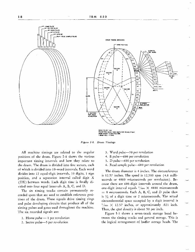
All machine timings are related to the angular positions of the drum. Figure 1-8 shows the various important timing intervals and how they relate to the drum. The drum is divided into five sectors, each of which is divided into 10-word intervals. Each word divides into 12 equal-digit intervals, 10 digits, 1 sign position, and a separation interval called digit X (DX) between words. Each digit time is finally divided into four equal intervals A, B, C, and D.
The six timing tracks contain permanently recorded spots that are used to establish reference positions of the drum. These signals drive timing rings and pulse developing circuits that produce all of the timing pulses and gates used throughout the machine. The six recorded signals are:
1. Home pulse - 1 per revolution 2. Sector pulse-5 per revolution
DRUM TIMI NG DIVISIONS
~ONE POSITION
--~*/
BASIC POL S( - eps
I \ SECTOR I \ I
I \ \
\ \
PULSE FREO-125KC 1&00 DIGITS PER REVOLUTION) ORUM SPEEO-IZ,.500 REV/MIN. I DRUM REV. - 'Ut MS.
Drum Timings
WI
w, DIGITS
3. Word pulse-50 per revolution 4. B pulse-600 per revolution 5. D pulse-600 per revolution 6. Read sample pulse-600 per revolution
The drum diameter is 4 inches. The circumference is 12.57 inches. The speed is 12,500 rpm (4.8 milliseconds or 4800 microseconds per revolution). Because there are 600-digit intervals around the drum, one-digit interval equals 1/600 X 4800 microseconds = 8 microseconds. Each A, B, C, and D pulse then is Y4 of a digit time or 2 microseconds. The actual circumferential space occupied by a digit interval is 1/600 X 12.57 inches, or approximately .021 inch. Thus, the spot density is about 50 per inch.
Figure 1-5 shows a seven-track storage band between the timing tracks and general storage. This is the logical arrangement of buffer storage heads. The
SECTION 1. GENERAL PRINCIPLES 1-9
actual arrangement of buffer storage is shown in Figure 1-6. This band is used for read-in and read-out buffer storage, called read-buffer storage (RBS) and punch-buffer storage (PBS), respectively. Both storages use the same band and the same heads for reading
and writing, but they occupy different portions of the drum circumference and are thus written into
and read from at different drum times. Digit values of words stored in read- and punch-buffer storage are represented in the bi-quinary system; thus seven tracks are used. Both storages have a capacity of ten words. All card input data enters general storage via RBS, and all output data from general storage must be punched via punch-buffer storage.
On read-in operations the parallel punched holes forming the digit notation of the words punched in the card are scanned by action of a cathode follower tube matrix and converted into serial form for stor
age in the 10 serial-word locations of RBS. At the same time the decimal punched hole notation is changed
to the proper bi-quinary form of representation. On read-out operations the serial pulses from the
PBS read circuits that form the bi-quinary digit notation of the ten words in PBS are converted into single, punch cycle timed, pulses and distributed to the proper punch magnet for punching in decimal notation by action of a thyratron punch scanning matrix.
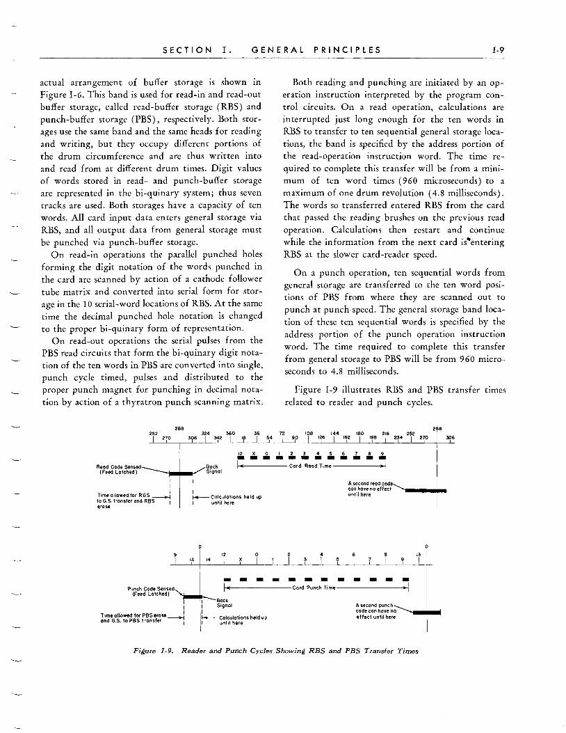
288 252
270 306
Both reading and punching are initiated by an operation instruction interpreted by the program control circuits. On a read operation, calculations are interrupted just long enough for the ten words in RBS to transfer to ten sequential general storage loca
tions, the band is specified by the address portion of the read-operation instruction word. The time re
quired to complete this transfer will be from a minimum of ten word times (960 microseconds) to a maximum of one drum revolution (4.8 milliseconds). The words so transferred entered RBS from the card that passed the reading brushes on the previous read operation. Calculations then restart and continue while the information from the next card is'-entering
RBS at the slower card-reader speed.
On a punch operation, ten sequential words from general storage are transferred to the ten word positions of PBS from where they are scanned out to punch at punch speed. The general storage band loca
tion of these ten sequential words is specified by the address portion of the punch operation instruction
word. The time required to complete this transfer from general storage to PBS will be from 960 micro
seconds to 4.8 milliseconds.
Figure 1-9 illustrates RBS and PBS transfer times related to reader and punch cycles.
288
270 306
~ x 0 123 4 5 6 7 8 9 ------------Reod Code Sensed (Feed Lotched)
I I
Time ollowed lor R BS ~ 10 G. S. Iransler and RBS I erase
Bock Signal
10( Cord Read Time »1 4 i I A second read code
I ~~~Ir~~~eno effecl ;-Calculotions held up I until here
9 12 0 4 6 e
Punch Code Sensed (Feed Lolched)
I I
Time allowed 10rpBserose~ and G.S. 10 PBS transler I
13 14 I X
- - -- -- - --- --I. Card Punch Ti me ) I I Back I Signal I k--- Calculalions held up I until here
A s.econd punch code can hove no effecl unlil here
13
I
Figure 1-9. Reader and Punch Cycles Showing RBS and PBS Transfer Times
o

1-10 IBM 650
One important limitation is imposed in transferring words between the buffer storage and general storage. The block transfer of ten words from RBS to general
storage is accomplished by switching together the RBS read output circuits and the general storage 'Zl/rite input circuits during the drum time that the words of RBS are passing their read heads. Similarly, a transfer of ten words from general storage to PBS is accomplished by switching together the general storage read output circuits and the PBS write input circuits during the drum time that the ten general storage words are passing their read heads. This means that only those
general storage word addresses that occupy the same drum sector as the words of RBS can receive informa
tion from RBS. Only those general storage word ad
dresses that occupy the same sector as the words of PBS can send information to PBS. Because there are 40 bands of general storage, there are 40 ten-word blocks or 400-word addresses, which can accept in
formation from RBS and 40 otlx1" ten-word blocks, which can send information to PBS. These addresses will be specified in the section on Programming.
If it is desired to store original data or instructions in any general storage location other than one of these 400, a transfer must be programmed. This programmed transfer is usually part of a pre-stored transfer routine that is used to distribute original in
formation to the desired general storage locations. Information to be punched must be placed by programming in one of the 40 general storage ten-word blocks associated with PBS. Notice that word locations in RBS and PBS are not addressable but func
tion automatically on programmed read and punch
operations.
The gray areas of Figure 1-4 show the general
storage positions that can be entered from RBS and those that can read out to PBS.
Stored Programming
The 650 uses a system of stored programming to provide the necessary sequence of operations for the solution of a problem. Unlike previous machines that utilized control-panel wiring of a program device, the 650 refers to any of its own storage locations to ob-
tain a previously stored or computed ten-digit, coded instruction word whose digit values can be interpreted by the machine to determine what its next
operation should be.
Original data and instructions are stored in drum storage locations from punched cards during the load
ing process. Additional data and/or instructions may be inserted from cards during the solution of the problem. Each instruction (program step) is stored
as a word. Because both data and instructions are stored in the same manner, an instruction word can be subjected to arithmetical operations and thus can
be altered by programming. The meaning of any valid coded instruction is built into the machine. Any sequence of instructions is called a program, or program routine.
All instructions are in the form of ten-digit words. The sign is carried along for checking purposes. It has no effect on the meaning of the instruction but must be considered when the instruction word is al
tered arithmetically.
The instruction word is divided into three sections (Figure 1-10). Digit positions 10 and 9 are the operation code, which tells the machine which of its several operations to perform on this program step. Positions 8- 5 are the n-address and usually mean either the loca
tion of information to be used in the operation, or the location where the information is to be stored as a result of the operation. In certain operations the naddress may have one of the following meanings:
1. The number of positions to be shifted either right or left.
2. The general storage band where the contents of the ten-word positions of RBS are to be entered on a read operation. Anyone of the 50 addresses of a band used as the n-address of a read instruction word will cause a transfer of the ten RBS words to the word 1
through 10 locations of the band.
3. The general storage band from which informa
tion is to be punched. Anyone of the 50 addresses of a band, used as the n-address of a punch instruction word will cause a transfer of the contents of word positions 27 through 36 of the band to the ten-word
positions of PBS. The transferred information will be punched from PBS.

SEC T 1.0 N I. GENERAL PRINCIPLES 1·11
010 09 08 07 06 os 04 03 02 01
Ixlxlxlxlxlxlxlxlxlxl v
Operation Code I' V ----" 'V I
Data Address Instruction Address
Typical Instruction words: 1 S 1726 1972 = Add to Lower Accumulator, without
reset, the contents of Storage location 1726 and use the contents of 1972 as the next instruction
20 1831 0734 = Store contents of Lower Accumulator . in Storage location 1831 and use the
contents of 0734 as the next instruction
Figure 1·10. Instruction Word Meaning
4. The location of an alternate instruction when selected by a branching operation. In any case the meaning of the n-address depends upon the associated operation code.
Positions 4-1 are the I-address that indicates the location in storage of the instruction word for the next program step, unless a branching operation has indicated the n-address is to be used for this purpose.
The following list shows all of the addressable storage locations in the 650:
Address
0000-1999 8000 8001 8002 8003
Location
General storage Control console storage entry switches Distributor Lower accumulator Upper accumulator
A more complete summary of addresses and opcodes will be found in a later section on Programming.
Logical Organization, Data Flow, and Program Control
The general logical arrangement of the machine is shown in Figure 1-11. The principal functional units and the various paths of information flow are shown.
It should be remembered that, although the data flow paths in Figure 1-11 are shown as a single line to simplify the illustration, each data flow path actually comprises seven parallel lines. In accordance with the bi-quinary system, information pulses representing
the numerical value of each digit will be present on two of these seven lines during each digit interval.
The preceding article on Drum Arrangement explains that the original data and instructions enter the ten-word RBS section of the drum after passing through the converter circuits where they are changed from the parallel, decimal notation of the punched card to the serial, bi-quinary form of RBS. A programmed read operation causes a block transfer of the ten words from RBS to one of 40 ten-word ge·neral storage blocks marked Card Read-In (Figure 1-11).
A programmed punch operation causes a block transfer of ten words from one of the 40 ten-word general storage blocks marked Card Punch-Out on Figure 1-11 to the ten-word PBS section of the drum. These 10 PBS words then pass through the converter circuits, where they are changed from serial, biquinary form to punch-unit timed impulses for punching into the card in parallel, decimal notation. Figure 1-11 also shows that all information entering the general storage section of the drum passes through a seven-to-five conversion matrix where the sevenbit, bi-quinary digit representation is changed to the five-bit code used for general storage. Similarly, all information leaving general storage passes through a five-to-seven conversion matrix where the five-bit representation is changed back to seven-bit, biquinary form. These seven-to-five and five-to-seven circuits are comprised of combinations of diode coincidence switches and diode OR circuits.

...... I
~
Storage Entry
Storage Exit
u Punch f
Converter
Address and OP 70 RQR8S 20's SlO
General Storage Read In Static Head Selection
5 to 7
(
8000 . 8001 8002 8003
Figure 1-11.
Ditploy Switch
650 Logical Schematic
(
I lU I I I I I I I I I
Adder "AM R. I. Switching
10'5 Adder MSM
R. I. Switching 10'. 6O's Except 69 35.36.84
r-------One Digit
Adder
l~U
Program Control
a,d OP84
TlU
OP & Addren Register R. I.
Switching
Program Control Circuits
Operation and Addren Registers
To OP code matrix for program control.
To storage selection and shift control.
10', 20·23
60's

SECTION 1. GENERAL PRINCIPLES 1-13
All of the arithmetical and logical operations that the machine can be programmed to perform such as add, subtract, multiply, divide, transfer of words to and from storage, shifting and logical tests are carried out by the action of the distributor, the accumulator and the one-digit matrix adder. The functionings of these units are controlled by the program control circuits of which the program step storage unit and the operation and address register are a part.
Each program step is performed in two parts, or half cycles. On the first part, or I half cycle, the operation and address registers are reset, and the 1-
address is placed in the address register where it is interpreted and used to select the location specified by the I-address. The new instruction word is then·read out of the selected I-address location and into the program register. On the second part of the program step, or D half cycle, the operation and address registers are reset, and the operation and data parts of the new instruction word now in the program register are read out of the program register and into the operation and address registers. Here the n-address is interpreted and used to select the n-address. The data word is then read out of the n-address location and into the distributor. The operation code is interpreted and activates the operation, which is performed using the data now in the distributor. This completes this
program step.
As soon as the operation is started, program control causes a return to the I half cycle. The operation and address registers are reset, and the I-address part of the instruction word in the program register is transferred 'to the address register, replacing the n-address, where it is interpreted and used to select the next I-address. The next instruction word is then read out of the I-address location and into the program register replacing the previous instruction word. The operation and address registers are again reset, and the operation and data parts of the new instruction word are read out of the program register and into the operation and address registers. At this point an interlock prevents further program advance except for read or punch operations, until the previous program step has finished using the arithmetic units. In this manner the machine advances through the steps of a stored program routine.
This half-cycle action, by which a program step is
performed, is accomplished by a program control
commutator, which controls the sequence of actions
necessary to advance through any program step (Fig
ure 1-12). This control commutator is a two-branched
ring with several positions in each branch. As it
cycles, it alternately advances through each branch.
The positions of one branch control the functions
of the I half cycle, while the positions of the other
branch control the functions of the D half cycle.
Normally the ring must advance through both branches, first I and then D, to complete a program step. The outputs of the steps of the control commutator are used to control the various transfers of data required for the accomplishment of the program step.
Program step storage (program register) and the distributor are capacitor storage units capable of storing serially, in bi-quinary form, the ten digits of a word and of making continuously available serially, a bi-quinary signal representing each of the ten digits in its proper sequence, once every word interval (1/50 drum revolution). Figure I-II shows that both units receive information from a common storage exit channel, but the switching into program step storage is open only on an I half cycle while that controlling entry into the distributor is open only on a D half cycle.
The main function of program step storage is to hold the instruction word that it receives from the 1-
address, and supply the proper part of this word to the operation and address registers for interpretation, at the proper time.
The distributor acts as a buffer between the accumulating components and addressable storage locations. Its main functions are to receive a word of data from a selected D-address and to make this word available to the accumulating circuits as required by the operation, or to receive a word of data from the accumulating circuits or the control console switches and make this word available for entry into a selected general storage location. The distributor is also an addressable storage location (8001) and can be used as a source of information, through selected storage switching, to supply an instruction word to the program register.
1-14 IBM 650
DX I Word Early DX Vi/ffi%'l//MW/M/?WA
Reslorl 10 "D" 1\ DX
--1 '-A Time -----.J Dynamic Sel L-- D9 DI
~ .Jl.. RIPS
DX DXBP
I---- Search 1- 49 Word Times -------!
"I" Alt.
OP Inllk Off
DI DX I Word Early D X
~/7D;n~;s;)M?JL- OP Inllk -"[i'Clri
D9 DI
~ JL~~~~I
DX
Code 69 . I Restor! to"( r--- Search 1-49 Word TImes ~ I
L ___ ~~~~~~ ______________________________________________________________ J DXL DI L ~nable Arith .Codes Sig.
Arith . IIO's and 60's)
Restort to"( 06
...F'L.
D6
Figure 1-12. Concept of Program Control Commutator
Capacitor storage units read out their stored information continuously during each drum word interval. This is done by driving the digit positions of the unit with drum timed-digit pulses from a drum driven digit ring. Each capacitor storage unit has a one-digitearly output and an on-time output. This is accomplished by driving each digit position of the unit with a drum time-digit pulse one-digit time in advance of the digit position of the storage unit. Thus, the digit-one position of the unit is read out at digit-zero drum time, digit two of the unit is driven at digit-one drum time, etc. Each early output is then delayed for a one-digit interval to provide an additional on-time output. Either output may be used depending upon the operation.
Capacitor storage units are a non-sustaining type of storage; i.e., each position requires periodic regeneration of its stored information. Regeneration is accomplished within the unit by providing a data flow path between the outputs of the unit and its input circuits. Thus, information that is available from the Dl position at digit-zero drum time is read back into the Dl position at digit-one drum time, etc., as long as the regeneration path is closed. Reading new information into a unit merely requires that the regeneration path be opened and that on-time output signals from the desired source be substituted at the storage unit input circuits in place of the units own on-time output signals. This is done whenever the input switching to the capacitor storage unit is activated.
SECTION 1. GENERAL PRINCIPLES 1-15
Figure 1-11 shows data flow paths from the outputs of all capacitor storage units. The information contained in any capacitor storage unit is continuously present serially, digit by digit, on these data flow paths. The data flow path from each of the capacitor storage units connects to the input switching circuitry of various other machine units; e.g., the distributor output connects to the adder B entry switching, selected storage switching, the control console light entry switching and the general storage entry switching. Reading information out of a capacitor storage unit requires merely that the entry switching for the desired receiving unit be opened for just the word time necessary to gate through the succession of output digit pulses representing the stored word.
The operation-code register is a two-position, biquinary, static storage unit. Each of its positions uses ') seven latches (electronic binary storage device) to in-dicate the operation-code value in bi-quinary form. It can accept information from the 9th and 10th positions of the program register on a D half cycle. Once a code is entered, a continuous, steady-state, biquinary output is available from two of the seven latches until the register is reset. These outputs are used in coincidence switching arrangements to control the indicated operation.
The address register is a four-position, bi-quinary, static storage unit similar to the operation code register. It can accept information from positions 5-8 o{ the program register on a D half cycle or from posi': tions 1-4 on an I half cycle. Its continuous, steadystate, bi-quinary outputs are used by the general storage read-write matrix to select statically the proper storage band for reading out 1- and D-addresses or for writing new information on programmed store operations and read operations. These outputs are also matched with the proper drum timing pulses by coincidence switching arrangements in the dynamic selection circuitry to select the proper word time for reading from or writing into a statically selected general storage band.
Operation code and address register outputs are also used as signals that help to control the advance of the program control commutator.
Figure I-II shows that information from these registers is also instrumental in controlling selected storage switching in those cases where it is desired to use
the control console switches, upper or lower accumulator, or the distributor as a source of information, rather than a general storage location.
The accumulator is a capacitor storage unit similar to the program register and the distributor, except that it has a two-word capacity. The serial digit signals of each word are available at their proper early and on-time drum digit times once every alternate word interval. The accumulator is divided into two halves for programming and calculating purposes, the low-order ten digits form the lower accumulator, and the high-order ten digits form the upper accumulator. Information in the lower accumulator is continuously available during each even-numbered drum-word interval, while information in the upper accumulator is continuously available during each odd-numbered drum-word interval.
Figure I-II shows data flow paths from the accumulator output to its own input, to one of the adder in-
• puts, to selected storage switching, to the distributor, and to the control console lights. Transfer of information from either half of the accumulator to one of these destinations is accomplished by controlling the read-in switching of the receiving unit to be open for the proper even- or odd-word time, during which time the output of the desired half of the accumulator is gated through the receiving unit.
The upper accumulator also can act as an overflow for the lower accumulator when a sum or product exceeds ten digits.
The main function of the accumulator is to work with the adder in accumulating sums, products, and quotients, and in performing shift operations. It also supplies zero-balance, plus balance, minus balance, and over-flow signals to the program control circuits for the logical test operations and can function as an addressable source of information (8002 or 8003) to supply an instruction word or a data word for programming purposes.
The one-digit adder is a diode and tube unit capable of receiving two input digit values, analyzing them, and producing a digit output signal equal in value to the sum of the two input values. The distributor and the accumulator feed into the one-digit adder. The output from the one-digit adder is stored back in the accumulator. A delay of one digit time is incurred between input to and output from the adder. An out-

1-16 IBM 650
put will be available from the adder only as a result of the entry of two input digits, one on each input line.
Digits from both the distributor and the accumulator can enter the adder-the distributor digits on one input line and the accumulator digits on the other. Provision is also made, in certain operations, for blanking the distributor or accumulator digit values and substituting zeros or constants for entry into the adder. Most calculator operations are performed by merging distributor and accumulator digit values or their substitutes in the adder and storing the result back in the accumulator. In most arithmetical operations the distributor and accumulator early output is used to produce an on-time adder output for the accumulator to store. In other operations such as shifting, the on-time output may be used.
Summary of Various Data Flow Paths
Digits can enter the distributor from any general storage location, from the entry switches on the control console or from either half of the accumulator. The selected storage path is used between the accumulator and distributor on arithmetical operations when the n-address is either half of the accumulator. The direct path is used on a Store-Accumulator operation. In this case the n-address is a general storage location meaning the destination of the word in the accumulator. The distributor can supply a word of information to the adder, to any general storage location, to the display lights on the control console (manual operation) ,or to the program register through Selected Storage switching.
The accumulator can be entered only from the output of the adder or from its own output (in certain shifting operations). The accumulator can supply information to the adder, the 'distributor directly, the distributor or the program register through selected storage switching, or the display lights (manual op
eration) . The program register can be entered from the com
mon storage exit line (either general storage output or selected storage) or from the adder on a table lookup operation. The program register can supply information to the operation and address registers, the display lights, or to the adder on a table lookup operation.
The operation and address registers can be entered from the program register. The operation and data part of an instruction word is transferred on a D half cycle, the 1 part on an 1 half cycle. The operation and address register static outputs control general storage head selection, the machine operation, selected storage switching, and the control commutator.
The adder normally accepts information simultaneously from the accumulator and distributor and supplies information to the accumulator. It can also receive data from the program register and read out to the program register on table lookup operations.
General storage can be read into from either read buffer storage or the distributor. General storage can read out either to PBS, the program register, the distributor, or to the adder on a table lookup operation.
The control console storage entry switches (8000) can read out to selected storage and thus to either the program register or the distributor.
The dotted lines on Figure I-II are the additional flow paths that are used only on the table lookup
operation.
Physical Organization
The machine is comprised of three basic physical units interconnected by cables. The 533 Read-Punch Unit, the 655 Power Unit, and the 650 Console Unit.
533 Read-Punch Unit
The 533 Read-Punch Unit is basically a high-speed punch similar to the 523 and the 402 Card Feed Unit, both mounted on a 528 base. The card reader is used to read information into the calculator, while the punch unit is used to record information taken from the calculator. The only control panel is on the 533 unit and is used primarily for designation and selection of input and output card fields, although some control of the calculator is possible. Input from the card reader is at 200 cards per minute. A maximum of 80 columns and 10 signs can be read from an 80-column IBM card. Selectors are provided to allow selection of input fields. Provision is made for card control of program routines.
The punch operates at 100 cards per minute. A maximum of 80 columns and 10 signs can be punched into an 80-column IBM card. Selectors that can be picked from the calculator are provided for output selection.

SECTION 1. GENERAL PRINCIPLES 1-17
655 Power Unit
The 655 Power Unit houses most of the power supply components used to provide the various necessary voltages. This unit also contains the read and punch scan matrices and associated circuits for converting to and from the parallel, decimal, punchedhole notation of the input and output cards and the serial, bi-quinary notation required by the drum storage.
650 Console Unit
The 650 Console Unit contains the magnetic drum, its associated read and write circuits and all calculating and program control circuits. In addition, it mounts the operator's control console, which contains switches and indicating lights for operation of the
machine.
Current Requirements, Dimensions, Weight, and Heat-Dissipation Data
Data given for machines manufactured prior to Ferbuary, 1956, except otherwise noted.
Approx. Height Width Length Weight
650 Console Unit 71" 307(/' 62Ys " 18001bs.
655 Power Unit 71" 307(6" 62Ys" 2400 lbs.
533 Read-Punch Unit 49 ~B" 2 5J{6" 5 7J{6" 1200 Ibs.
The power requirement is either 230 or 208 volts, with -+- 1 0 (A regulation. 1 OO-ampere service
50-60 Cycles 48,300 B.T.U./hour heat Single-phase or three-phase dissipation
Approximately 58,300 B.T.U./hour heat dissipation for machines manufactured after February,
1956.
Self-Checking
The accuracy of calculations is achieved by checking the transmission of all data and instructions to satisfy the validity requirement that there be one and only one bit in each level (binary and quinary) of a digit. Punched information is checked by doublepunch, blank-column-detection circuits. When a validity check error occurs, the machine may be stopped or the program routine may be branched to repeat a portion of the problem or to initiate a different problem.
Figure 1-11 shows the location of these validity check circuits, at the output of each of the capacitor storage units. Because all information eventually passes through these units, any invalid combinations will be detected.
In addition to these validity checking features, the program control circuits and the arithmetic circuits are designed with inherent checking features and fail safe logical arrangements as far as is economically possible. These control checks are dependent upon the proper combination of signals within the machine, the proper sequence of signals, double circuitry, and back signals, which insure that the signal to perform some operation was received and that the operation was completed before proceeding to the next step.
A special check assures that information is entered into only one general storage location on any general storage write operation.
Meaningless address and operation codes are detected and cause an error indication.
The timing rings are continuously checked on each cycle of their operation. Any timing error is detected
and causes a timing error indication. A continuous check is made of the accumulator for
an accumulator overflow or a quotient of more than 10 digits. An overflow condition can cause a machine stop or can be used to branch the program routine.

SECTION II. BASIC PRINCIPLES
PROGRAMMING
To SOLVE a problem on the 650, original data words and instruction words must first be loaded into storage locations on the drum from punched cards. The information to be punched in the loading cards is first written on a program sheet or planning chart in the numerical codes of the machine. Each line on this chart then represents either a word of data to be used on a program step or a word of instructions to be carried out on a program step. The coded information on each line of the chart is punched into the loading cards. Often several lines of coding are punched into several fields of one card and loaded into the specified storage locations by means of a previously stored loading routine.
Storage Address and Operation Codes
The addresses of all storage locations and the mean
ing of the operation codes follows:
Address Unit Addressed
0000-1999 General storage (General storage address can be either a source of information or a destination for information
depending on the OP-CODE meaning) 8000 Storage entry switches 8001 Distributor 8002 Lower accumulator 8003 Upper accumulator
General storage locations that are 111 the same angular position on the drum as word 0001-0010 can receive information from RBS. There are 10 words in each of the forty bands that can be transferred into from RBS (Figure 1-4).
There are other locations in general storage from which information may be transferred to punch bufer storage. These are the locations in each of the forty bands that occupy the same angular position
IJ-l
on the drum as PBS. The band is determined by using anyone of the fifty addresses within a band as the Daddress of the punch instruction. In the 0000 band the punch-out positions are words 27-36.
The two-digit operation codes represent the various built-in operations that the machine can perform.
In the case of the arithmetic codes (1 O's and 60's), the D-address of the instruction word specifies the' location of the addend, subtrahend, multiplicand, or divisor. In these operations the operand or operator is transferred from its storage location to the distributor. It is then added or subtracted into the accumulator as required by the operation. After the operation is complete, the original operand or operator remains in the distributor. The next instruction is taken from the location specified by the I-address.
In the case of store codes (20's), the D-address specifies the location where the number is to be stored. The information contained in a general storage location is automatically erased as the new number is entered. The stored number is also available in the distributor after completion of the store operation. The contents of the accumulator is not affected by a store operation.
Summary of Operation Codes
The following summary of operation codes is provided, without the detailed description, for easy reference.
To simplify the use of these codes, and as an aid in understanding the program control circuits, which will be considered in a later section, notice that the operation codes can be grouped into seven classifications according to their meaning. Also notice that each of the codes in one of these seven classifications has a common ten's position numerical value. Remember that within the machine, the codes and addresses appear in their bi-quinary form in the operation code and address registers where they are interpreted.

11-2
O's
10's
and 60's
20's
30's
40's
and 90's
70's
IBM 650
Code Abbreviation Operation
00 01 10 11 14 15 16 17 18 19 20 21 22 23 24 30 31 35 36 44 45 46 47 60 61 64 65 66 67 68 69 70 71 72 84 90 91 92-99
NO-OP and STOP
NOOP STOP AU SU DIV Al Sl AABl SABl MUlT STl STU STDA STIA STD SRT SRD SLT SCT BRNZU BRNZ BR MIN BR OV RAU RSU DIV RU RAl RSl RAABl RSABl LD RD1 WR1 RC1 TlU BRD 10 BRD 1 BRD 2-9
No Operation Stop Add to Upper Subtract from Upper Divide Add to lower Subtract from lower Add Absolute Value to lower Subtract Absolute Value from lower Multiply Store lower Store upper Store lower Data Address Store lower Instruction Address Store Di stri butor Shift Right Shift and Round Shift left Shift left and Count Branch on Non-zero in Upper Branch on Non-Zero Branch on Minus Branch on Overflow Reset-Add to Upper Reset-Subtract from Upper Divide-Reset Remainder Reset-Add to lower Reset-Subtract from lower Reset-Add Absolute Value to lower Reset-Subtract Absolute Value from lower load Distributor Read into Input Storage Area 1 Write (print or Punch) from Output Storage Area 1 Read Conditional into Input Storage Area 1 Table lookup Branch on 8 in 10th Position of Distributor Branch on 8 in 1st Position of Distributor Branch on 8 in 2nd through 9th Position of Distributor
Figure II-I. Operation Codes
84
Arithmetic codes. Notice that binary value of the ten's position determines the resetno-reset meaning of the code. The quinary part of the ten's position and all of the units positions are the same.
Table Lookup. Only one code is used in the 80 series
Figure II -1 shows the operation codes and abbreviations that are used in the 650.
Examples of Programming
Store codes
Shift codes
Test codes. Here the binary value of the ten's positions determines whether the accumulator or the distributor is to be tested.
Input and Output codes
To explain the use of the addresses and operation codes, a simple problem is shown. Figure II-2 shows the lines of coding that might be used to solve the
I (A + B -C) D prob em E
In this example the values of the factors are:
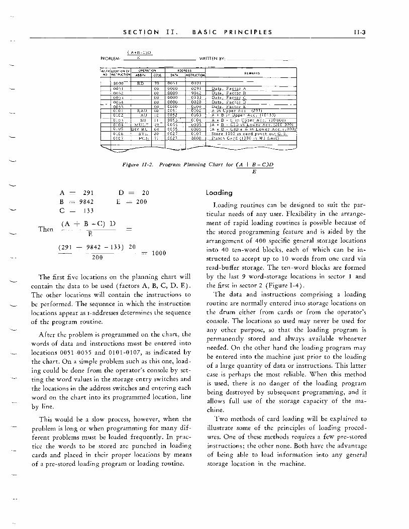
SECT!ON II. BASIC PRINCIPLES 11-3
( A+B-C)D
PROBLEM __ --=E=--_______ _ WRITTEN BY: _________ ~
INSTRI~CATION OF OPERATION ADDRESS NO INSTRUCTION ABBR" CODE DATA INSTRUCTION
REMARKS
"l K IU 000 onr 0651 00 0000 0291 Data, Factor A 0052 00 0000 Q842 Data Factor B 0053 00 0000 0133 Data Factor C 0054 00 0000 0020 Data Factor D 0055 OC 0000 0200 Data Fac tor E 0101 RAU 0051 0102 A in U er Ace 29 0102 AU 10 0052 0103 A + B In Upper Ace. 10133 0103 SU II 0053 .0104 A + B - C In UDPer Ace. (10000) 0104 MULT 19 0054 0105 :~ : : ~ ~ ~ ~nEL~:~~:;:.)~~~ i~ 0105 IV RU 64 0055 0106 0106 STL 20 0027 0107 Store lOaD 1Il card Duncn out~~ 0107 PCH 7 I 0027 8000 Puncn Card 1000 In Wl fIeld)
.... -'-.. ----------
-==
Figure JI-2. Program Planning Chart for (A + B - C)D
E
Then
A B
291
9842
C 133
(A + B ~C) D
E
D = 20
E = 200
(291 + 9842 ~ 133) 20
200 - 1000
The first five locations on the planning chart will contain the data to be used (factors A, B, C, D, E). The other locations will contain the instructions to be performed. The sequence in which the instruction locations appear as I-addresses determines the sequence of the program routine.
After the problem is programmed on the chart, the words of data and instructions must be entered into locations 0051-0055 and 0101-0107, as indicated by the chart. On a simple problem such as this one, loading could be done from the operator's console by setting the word values in the storage-entry switches and the locations in the address switches and entering each word on the chart into its programmed location, line
by line.
This would be a slow process, however, when the problem is long or when programming for many different problems must be loaded frequently. In practice the words to be stored are punched in loading cards and placed in their proper locations by means of a pre-stored loading program or loading routine.
loading
Loading routines can be designed to suit the particular needs of any user. Flexibility in the arrangement of rapid loading routines is possible because of the stored programming feature and is aided by the
arrangement of 400 specific general storage locations into 40 ten-word blocks, each of which can be instructed to accept up to 10 words from one card via read-buffer storage. The ten-word blocks are formed by the last 9 word-storage locations in sector 1 and the first in sector 2 (Figure 1-4).
The data and instructions comprising a loading rou tine are normally entered into storage locations on the drum either from cards or from the operator's console. The locations so used may never be used for any other purpose, so that the loading program is permanently stored and always available whenever
needed. On the other hand the loading program may be entered into the machine just prior to the loading of a large quantity of data or instructions. This latter case is perhaps the most reliable. When this method is used, there is no danger of the loading program being destroyed by subsequent programming, and it allows full use of the storage capacity of the machine.
Two methods of card loading will be explained to illustrate some of the principles of loading procedures. One of these methods requires a few pre-stored instructions; the other none. Both have the advantage of being able to load information into any general storage location in the machine.

II-4 IBM 650
B003 Upper Accumu iafo r
Block Co rd .....: locction Instruction Opero tion No. No. ~ Instr~fd ion OP Dolo In~ tr . Abbrev.
~!~:r~~~e Codes
8002 l ower ACCll mvlolo r
B001 Dist rib utor Remorb
8000 70 000] 0058 R D Re a d . Ii load card go to 0001 for next matr . Q-Normal 0001 69 0004 0003 LD L oad Distributor with instr. to be stored
Instruction 1--_+--++,O~OO~3~l=-,4+-:.:.:.=-+,8",O~0004~ST'..!D'---++-t-++-l+-H-+t-+-t-1+-H-+t-+-rH-++-t--H-+t-+---=:Stc:.or=-::e-'i::.:ns:::tr:.::u::..:ct=io:::.n..:.:in:...:s'-"p.:..:e c:::iC::.:ie:.::d..:.:lo:.::c::.:at::.:io:::.n.'--_-I
3-Sheet Heading
I L OA DIN G RO UT INE - ON E WOR D PER CARD
S ET - UP
1. S e t Sto r ag e E n t ry Switches to 700001 0058 3. P ress Computer Re set Key
2 . Se t Cont rol Swi tch to RUN 4. Pr ess Pro g r am Start Key
Figure Jl-3. Loading Routine-One Word per Card
Figure II-3 shows the planning chart and card arrangement for the simpler of these loading procedures. With this method, one word of a planned routine is loaded per card. Thus, one loading card will be required for each line of coding on the planning chart of the problem to be solved. No previously stored instructions are necessary for this routine. Only one control-panel wire is necessary from the column, which contains the loading card identification, to the LOAD hub.
This wire does two things: 1. Allows the word 1 field of the card (cols. 1-10)
to enter storage entry 1 (first word position of RBS) , word 2 field (cols. 11-20) to enter storage entry 2 (second word position of RBS), etc. These entries are accomplished without any column to storage con
trol-panel wiring. 2. Indicates to the calculator that the card was a
loading card, so that the next instruction will be taken from the D-address of the read instruction instead of the I-address.
After these cards are punched, they are placed in the read hopper, face down, 12-edge first. The read start key is depressed, resulting in three run-in cycles, at which point the read start key is no longer effective.
During the third run-in cycle the information in the three punched word fields of the first load card has automatically entered the first three word storage positions of read-buffer storage, and the load card back-signal control relay has been picked.
As shown in Figure II-3 the first instruction of the loading routine (70 0001 0058) is set in the storage-entry switches on the control console (location 8000). The control switch is set to RUN, and the computer reset key is depressed. This use of the computer reset key, resets the program register, distributor, and accumulator to zeros and, because the control switch is in the run position, resets the address register to 8000. It also insures that the control commutator will begin in an I half cycle. The program start key is depressed, allowing the control commutator to advance through its I half cycle. Because the address in the address register is 8000, the contents of the storage-entry switches will be transferred to the program register on this I half cycle. Upon completion of this transfer, the control commutator will signal a restart to D, and during the restart word time the
OP and D portion of the instruction in the program register will be placed in the operation code and address registers (70 0001).
SECT.ION II.
At the end of the restart word time, the 70 output from the operation code register will cause an advance read feed signal and will energize the readbuffer storage transfer and erase control circuits, resulting in a transfer of the contents of RBS to the card read-in positions (words 1-10) of the general storage band indicated by the address register (0001 band 0000-0049), and the subsequent erasure of RBS to blanks. This transfer and erase action occurs while the read clutch is being energized and during the first few degrees of the reader cycle. At 300 0 a reader cam (R57) sends a back signal to the backsignal control relay. As this relay is up, because of the load card impulse on the last reader cycle, the cam back signal is diverted from its normal restart action to a Use D signal.
The Use D signal flips the alternation control latch of the control commutator, removing the D signal and replacing it with an I signal, so that as the commutator advances from the restart word it will proceed through its I branch. No restart signal is given; thus the operation and address registers are not reset. As the commutator advances through its I half cycle, the address in the register is still the D-address of the read instruction (0001). This address now is used as the location of the information to be read into the program register.
Because 0001 now contains the first word of the first load card (69 0004 0003), this instruction is read into the program register, and a restart to D is again signalled. Note that if the back signal control relay had not been up, a normal restart to I would have occurred, resulting in a reset of the operation and address registers and a transfer of the I-address of the read instruction (0058) to the address register. The next instruction would then have been read into the program register from location 0058 instead of 0001.
During the restart word the operation and address registers are reset and the operation and D parts of the instruction in the program register are placed in
the operation and address registers (69 0004). During the D half cycle the operation and address register outputs signal the head selection circuits to choose general storage band 0000-0049 and the control commutator to open up distributor read-in switching at such a time that the contents of 0004, which is the word to be loaded, will be transferred to the distribu
tor.
BASIC PRINCIPLES 11-5
Upon completion of the distributor read-in, a restart to I is signalled, the I-address (0003) is placed in the address register and the next read-in to the program register is from 0003 (24-8000). On the next D half cycle the word to be loaded, now in the distributor, is placed in the specified D-address by the direction of the store distributor, operation code 24. The next instruction is taken from the switches, which feeds another card and causes a repetition of these steps. In this way the information required for the problem is placed in the general storage locations specified by the problem planning chart.
During the D half cycle in which the last load card information is transferred from read buffer storage to general storage, the following data card passes the second brushes. Data cards do not contain the load card 12 punch. Therefore, when the machine completes the next code 70 (code 70 for the first data card) D half cycle, a normal restart to I is sig
nalled. In this example location 0058 was arbitrarily chosen
as the I-address of the read instruction. Any other general storage location could be used.
With this procedure, one word can be loaded per card. It would require 2000 cards to load the machine to capacity. Because cards feed through the reader at 200 cards per minute, it would require 10 minutes to load the machine. The disadvantage is the relatively large number of cards to be punched and verified.
Figures II-4 and II-5 show a planning chart and card form for a loading procedure that can load up to four words from one card in any general storage
location. This program will load the information punched in the word 1 field of the card into the location specified by the D-address of word 2; word 3 into the D-address of word 4; etc. This procedure requires that the I-address of the last instruction be 8000.
In the card shown, four words are to be loaded. If fewer than four words are punched, the I-address of the last instruction on the card, whether it be the first, second, or third must be 8000. This loading routine requires that locations 1950, 1961, 1962, and 1963 contain the pre-stored instructions and constants indicated on the planning chart. This information can be initially placed in these locations manually from the the control console or by means of the previously described one-word-per-card, loading routine.

11-6 IBM 650
LOADING ROUTINE - FOUR WORDS PER CARD
SET - UP
1. Set Storage Entry SWitches to 701')61 (XXXX)o Z. Set Control Switch to "RUN"
3. Pre •• Computer Reset Key 4. Pre •• Program Start Key
Location In!otruction Operation 8003 8002 8001 1i of QC I IfU fion op Da'. Insfr. Abbrev. Upper Accumulator lower Accumulator DIStributor Remarks
8000 70 1961 XXX» RD into 1951-1960 if load card use 0 ,/ 1961 65 1962 1950 o (
21 ¥ RAL from 1962
1950 15 1963 8002 o 0 ~~ 2 .ilL from 1963 1st {
'" 8002 69 1951 1952 F LD from 1951 Word 1 from card 1952 24hcXX>O 1950 STD in XXXXI Word 1 now in (XXXX)
Word
o 0 o 0 o 2 o 0 o 2 1950 15 1963 8002 .ilL from 1963 8002 69 1953 1954 6 1 1 LD from 1953 Word 3 from card 1954 24 XXXJQ 1950 STD ;.'1 XXXX Word 3 now in (XXXX)z
2nd { Word
o 0 o 0 o 2 o 0 o 2 1950 15 1063 800> .ilL from 1963 8002 60 1055 1956 LD from 1955 Word 5 from card 1956 24 XXXJQ 1950 STD 111 XXXX3 Word 5 now m IAAAAl3
3rd { Word
o 0 o 0 o 2 o 0 o 2 1950 15 1963 8002 .ilL from 1963
8002 60 1057 1058 LD from 1957 Word 7 from card 1958 24 XXXXI 8000 STD in XXXX4 Word 7 now in (XXXX)4
4th { Word
8000 70 1961 XXXJQc RD into 1951-1960 if load card use 0 (Repeat) Repeat {
Iv 1962 69 1949 1950 Data Skeleton Instruction
'" 1963 00 0002 0002 Constant To modify skeleton matr.)
NOTE: (XXXX)o can.e the starting address of the problem to be solved.
NOTE: V shows pre-stored information and addresses where stored (1950~ 1961~ 1962:~ 1963).
Figure 11-4. Loading Routine-Four Words per Card
An advantage of this loading procedure is that it can load the machine with fewer cards. Only 500 cards would be needed to load the machine to its capacity. It retains the flexibility of being able to place any word in any storage location, an advantage when loading optimum-coded program routines. Notice that this procedure makes use of the machine's ability to alter instructions arithmetically.
Other routines can be devised that will load up to seven 10-digit words per card, one field being used for a loading instruction. These procedures, however, are usually subject to the limitation that the location of the first word on the card is specified, and the remaining words will be placed in successive or constantly spaced storage locations. The only advantage is the decrease in the volume of load cards to be punched and verified, because actual machine loading time, even at the rate of one word per card, is usually a negligible part of the total time required to solve a problem.
Refer to the planning chart for the sample problem
(A + B -C) D (Figure 11-2)
E
The lines of coding that make up this problem could be loaded by using either of the two preceding loading procedures. The cards that would be required to load this problem, using the four-word-percard routine, and factor cards for the solution of two problems, are shown in Figure 11-6. To start this problem these cards are placed in the read feed hopper, face down, 12-edge first. The read start key is used to feed the first card past the second brushes. At this point its information will be in the first eight word positions of read-buffer storage. The four steps of the setup procedure of Figure 11-4 are then performed, and the data and instructions contained in the cards are entered. In this case 0101, the starting address of the problem, is used as the I-address of the read instruction word (XXXX) set in the switches.

LOAD PUNCH
[]
ADDRESS WHERE WORD I IS TO BE STORED (KEY PUNCHED)
ADDRESS WHERE WORD 3 IS TO BE STORED (KEY PUNCHED)
ADDRESS WHERE WORD 51S TO BE STORED (KEY PUNCHED)
ADDRESS WHERE WORD 7 IS TO BE STORED (KEY PUNCHED)
24(XXXXI,1950 24(XXXX121950 24(XXXX131950 24(XXXXI4800c
FIRST WORD SECOND WORD THIRD WORD FOURTH WORD 10 BE STORED 10 BE STORED TO BE STORED TO BE STORED (KEY PUNCHED) (KEY PUNCHED) (KEY PUNCHED) (KEY PUNCHED)
WORD I WORD 2 WORD3 WORD 4 WORD 5 WORD 6 WORD 7 WORDS
1011 2021 3031 4041 5051 6061 7071
+ 1951 +
1958 + 1956 + 1957 + 1954 + 1955 + 1952
+ 1953
Figure II-S. Card for Four-Word-per-Card Routine
000000026100000097930000001254100000000020000000275 o 0 o
o o o
WORD 1 WORD 2 WORD 3 WORD -4 WORD ~ WORD 6 WORD 7 WORD 8
o 0 0 0
0000000291 0000009842 0000000133'00000000200000000200 o I o
WORD 1 WORD 2 WORD 3 WORD "' WORD !I WORD 6 WORD 1 WORD a 00000 0
II~~~~ 10~ 2~:~~ 195~20~~~~0 10 24~~~~ 1950 71 ~~~:8000 24~:~~8000 WOR,1 0 WORD.
o 01 0 0 0 0 0 0
6000510102 240 10 1195~ 1000520 103 2401021950 1100530104 2401031950 1900540105 2401048000 I I
WORD 1 WOR D 2 WOAD 3 WORD 4 WORD !I WOII:O 6 WORD 1 WORD 8
0 00 0 0 0 0 0
0111001010001010000 0111001010001010000 0011001010001010000 00110010100010100"
11 ::;; i; i; ~O ~I~2 ~J I~S il;8;9~11;2;J;4;~~;' i77~1~;J i;~~ I~;g7il;J ~;J ~;' i;9~~I~~i;5~ SI~;9~i~~7;5~;l i;9~O ;I;2~Ji;S;S;';8;9;0' IBM TYPE 650 MAGN[ TIC DRIJM DATA PROCESSING MACHINE
22222222211222222222122 I I I I 2222222222221222222222
3333333333333333333333 I I 3333333333333333333333
4444444444414444444444
155 5 515 5 5 5 515 5 5 5 5 5 5 515 5 5
116 6 6 6 6 6 6 6 6 6 6 6 6 6 6 6 6 6 6,6 6
'7777777777777777777777
4 4 4 4 4 4 4 14 4 4 4 4 14 4 4 14 4 4 4
15 '15 5 5 5 15 5 5 5 5 5 5 5 5 5 5 5 5 5
6666666666666666666666 1
7 77 7777777777777777777
8 8 8 8 8 8 8 8 8 8 8 8 8 8 8 8 8 8 9 8 8 8 8 8 a 8 8 8 8 8 8 8 8 8 8 8 8 8 8 8 18 8 8
9999999999199999991 99 i99 I 1999199999999 ,9999999999 1 2 3 4 5 , J • 910 11111!) 14::; If 1111 !!]C ,1! n 1~:,}" J~ n i8 n ~ 1 )1 J1 33 J( lS 3631 J839 401414] 43 44 4S 46 4148 49 ~ISI 52 ~l ~~ ~s 56 ~ 1 ~8!9 ti(ltbl ~? 63 64 6S 66 6168 6910:11 11 1314 15 16 HIS 19 811
IIM86 2 1BO X
Figure lJ-6. Loading Cards for (A + B - C)D E
11-7
80

II-8 IBM 650
Thus, the machine automatically starts processing the problem upon completion of the loading routine.
If it is desired to stop the machine after loading before proceeding with the calculations, an address containing a pre-stored stop instruction (01 0000 0000) can be used as the I-address (XXXX) of the read instruction set in the switches. The machine can
then be started by setting the starting address of the problem in the address selection switches and using the transfer key to transfer this address to the address register. The program start key will then start the calculator, which will take its first instruction from the location in the address register (0101).
An alternative method of starting the machine would be to set a NO-OP code in the storage-entry switches, with the starting address of the problem as its I-address (00 0000 0101). Set the control switch to the run position. Depress the computer reset key to reset the address register to 8000. Depress the program start key to start the calculator, which will then take its first instruction from the storage-entry switches. This instruction (00 0000 0101) will cause the machine to restart to I and take its next instruction from 0101, thus starting it on the sequence of the problem's program routine.
BASIC ELECTRONIC CIRCUITS
THE BASIC functional electronic circuits used in the 650 are few and simple. The computing circuits are designed to employ twin triode tubes and germanium crystal diodes. In the computing circuits tubes are used functionally as inverters, double inverters, and cathode followers. Elsewhere in the machine, triodes are used as voltage amplifiers, shaping amplifiers, power units, and single-shot multivibrators. Thyratrons are employed in the read-out circuitry. Inverters and cathode followers are connected by external circuitry to form a latch circuit. Latches are used as a substitute for triggers where a momentary signal must be stored for later use and in timing ring cir
cuits. The logical circuits of the 650 make extensive use
of germanium crystal diodes arranged to act as positive signal AND circuits and positive signal OR circuits.
Hereafter, to avoid confusion due to multiple usage of the terms AND and OR, AND circuits will be referred to as switches and OR circuits will be called mixes.
Crystal diodes are also used occasionally to clamp tube grid voltages at a fixed level.
Double-diode vacuum tubes (6AL5) are used in some circuits where applied voltages are too severe for crystal diodes or where the back resistance of a crystal diode is too low for proper back-circuit elimination.
Capacitor storage is used in the accumulator, distributor, and program register where rapid access to the stored information is essential. In the capacitor storage unit a capacitor and two associated vacuum diodes form a basic binary storage device, combinations of which are used to build up the one- or twoword storage unit.
Inverters and Double Inverters
The basic characteristic of an inverter is implied in its name. A signal applied to its grid is reversed in
polarity or inverted at the plate end of its load resistor (Figure 11-7). The signal is usually also amplified in the process because of the tube's characteristics. The voltage levels, between which the inverter's output signal swings, are relatively high (typical values are plus 150 to plus 50 volts although lower amplitudes are often obtained by tapping the plate load resistor). The load resistance, across which the output signal is developed, is relatively high (typical value, 20K). Thus, the inverter is a high-impedance device whose output signal is rather easily distorted by associated circuit capacitance.
A double inverter is merely two coupled inverter stages where the plate output signal of the first drives the grid of the second. In a double inverter the signal is inverted twice so that the final output is of the same phase as the input signal. The coupling between stages may be direct or capacitive. If direct, the output signal has the same duration as the input. If capacitive, a pulse output signal is obtain.ed even though the input may be of relatively long duration.
In the 650, inverters are largely used to restore the level of signals that have been altered by passage through diodes and cathode followers. The output signal of a double inverter is usually used to operate the

SECTION II.
+150 ·'~u +50
20K
+IOJL
-35
Single Inverter
+150 +15OU
+50
200K
lOOK
-50
Direct Coupled Double Inverter
Capacitor Coupled Double Inverter
Figure 11-7. Inverters
grid of a cathode follower whose output is a low-level,
low-impedance, restored signal as in Figure II-S. Inverters are sometimes used to block a signal that
20K
+150 +15OlJ
Altered +50 Signol
+20n -25
Note: Normal .lgnal level Is -35 10 +10
+150 +15On +50
Rl
+150
+7n -38 Restored
Signal +10 n -35J L
Figure II-B. Signal Level Restoration Using Double Inverter and Cathode Follower
BASIC PRINCIPLES
+150
Figure II-9. Blocking Inverter
11-9
810cked by B
J1illbcr',de I I I I
would otherwise be available. In Figure II-9 a positive output signal from tube A is periodically available except when tube B is caused to conduct through the common load resistor, thus holding the plate potential down and preventing tube A's plate voltage from rising to signal level.
Cathode Followers
A cathode follower is a tube, usually a triode, with circuitry arranged so that the output signal is taken from the cathode end of a cathode load resistor (Figure II-lOA). As its name suggests, the output signal follows or is in phase with the grid input signal. A cathode follower is inherently a negative feedback device, i.e., for values of grid voltage between cutoff and saturation, as the grid voltage is increased the cathode voltage also increases due to the increased IR drop across the cathode load resistor. The net result is a self-biasing action that limits the amplitude of the output signal to a value very nearly equal to the am
plitude of the input signal. The amount of bias de
veloped depends upon the tube characteristics and the load resistor value.
+150 +150 +150
A or 8
n
Figure II-lO. Cathode Followers

11-10 IBM 650
In any case the cathode reaches an equilibrium potential more positive than the grid. Thus, a signal will gradually have its levels raised as it passes through a series of cathode followers. Cathode follower load resistors need not be as large as those used for inverters, because the value of the load resistor has less effect on the amplitude of the output signal. Thus, a cathode follower can be a relatively low impedance device whose output signal is less susceptible to distortion by associated circuit capacitance. In the 650 the voltage levels between which a cathode follower output signal swings are commonly of the order of minus 35 to plus 10 volts.
An important point to note in connection with cathode followers as used in the 650 is that, unlike inverters, the tube is always conducting whether the grid is at the no-signal level (- 35) or the signal level (+ 10), because the cathode resistor is returned to a voltage value more negative than the no-signal
level. Cathode followers are frequently used with double
inverters for dc signal-level restoration (Figure II-8). They are also often used to give a signal, whose levels are still usable, more drive after it has been attenuated by passage through a series of diodes.
Tw@ cathode followers may share a common load resistor and thus form a logical OR circuit where either signal A or signal B will produce a similar output (Figure II-lOB).
Germanium Crystal Diode Switch and Mix Circuits
Diode AND Circuits
Germanium diodes are widely used in switching circuits in the 650. There are basically two types of switches, those requiring the presence of two or more signals to give an output and those requiring the presence of anyone of several input signals to give an output. The first type is called a switch and the sec
ond type is referred to as a mix.
The diagram shown in Figure II-II illustrates a diode switch circuit. Switches Sl and S2 are the inputs to the diodes, and the output is taken from the common plates of the diodes. The input signals can be either - 35 volts or + 1 0 volts.
+75V
Output
+IOV
IOV
n35V -35V
Figure 11-11. Diode AND Circuit
I"putt
Block Symbol
With SI and 52 set to position A as shown, the diodes are connected to - 35 volts. The output voltage will be effectively - 35 volts because of the low forward resistance of the diodes. Current can flow from the - 35-volt level up through the diodes in parallel, through the load resistor and to the +75-volt poten
tial. Practically all of the voltage drop will be across the load resistor so the output will be - 35 volts.
If 51 is now thrown to B, the potential across the D2 branch is the greatest. The output is still effectively connected to the - 35 volts through ,the low forward resistance of D2 so the output is - 35 volts. When 52 is also thrown to position B, both diodes are connected to + 10 volts, and the output will now be + 1 0 volts.
Notice from this it was necessary that both inputs be up to the + 1 0 volts level before the output could come up. Also note that the output is controlled by
the branch of the circuit that has the greatest voltage drop across it.
This type of switch circuit may have from two to about five inputs.
Diode OR Circuit
Figure II-12 illustrates a diode mix circuit. With 51
and 52 set to A as shown, the output will be - 35 volts. In this condition the output is connected through the diodes in the forward direction to the - 35-volt potential. The low resistance of the diodes is negligible compared to the load resistor, so that the ou tput is effectively - 35 volts.

40V
35V
r-3: ~ - 10V
-75V
Sl
-35V
+lOV
SEcnON II.
Output
:ff Inputs
Block Symbol
Figure II-12. Diode OR Circuit
If switch 51 is set to B, the output is now connected to + 1 0 volts through the diode Dl in the forward direction. This caused the output to be effectively + 1 0 volts. The same would be true if 52 had been set to B. Diode D2 would then connect the output
to the + 1 o-volt potential.
With this type of circuit, notice that either input going up to + 1 0 volts causes the output to go up to + 1 0 volts. In this circuit, as in the diode switch cir-
+ 70
T 150 A & +150
+150
Electron Flow -70 -70
BASIC PRINCIPLES 11-11
-50
cuit, the output is determined by the branch of the circuit that has the greatest voltage drop across it.
The diode mix is used when one of the several input signals is to control a given function. The mix prevents any back circuit or interaction between input signals. One mix may have from two to nine inputs.
50me typical connections using diodes to form switch circuits, mix circuits, and comqination switch and mix circuits are shown in Figure II -13. Consider the switch circuit. Ass~me that the A signal is - 35 volts and the B signal is + 10 volts. The source impedance of signal A in series with the forward resistance of the diode is sufficiently low in comparison to the resistance R to hold point X at a minus potential. The back resistance of the other diode is high enough to prevent the plus B signal from raising the potential at point X. Thus, point X will rise to a plus potential only when both signals A and B are at plus potential.
In the mix circuit a plus B signal will raise point X to about the signal potential (plus 10 volts) because the combined diode forward resistance and the signal B source impedance is small in comparison to resistance R. The minus A signal has no effect on the
-50
A OR
+150
-35
-70
OR + 70
& &
ABC 0 '----v-----"
+ 10'0-35 Volt Signals
Switch and Mix Both A and 8 to 9 i .... e output or both C and 0 to give output
Switch Mix Both Itt. and B to Either A or B to give output give output
Figure II-13. Crystal Diode Switch and Mix Circuits
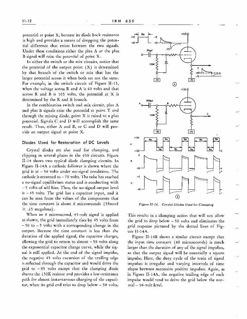
11-12 IBM 650
potential at point X, because its diode back resistance is high and provides a means of dropping the potential difference that exists between the two signals. Under these conditions either the plus A or the plus B signal will raise the potential of point X.
In either the switch or the mix circuits, notice that the potential of the output point (X) is determined by that branch of the switch or mix that has the larger potential across it when both are not the same. For example, in the switch circuit of Figure II-13, when the voltage across R and A is 60 volts and that across Rand B is 105 volts, the potential at X is determined by the Rand B branch.
In the combination switch and mix circuit, plus A and plus B signals raise the potential at point Y and through the mixing diode, point X is raised to a plus potential. Signals C and D will accomplish the same result. Thus, either A and B, or C and D will provide an output signal at point X.
Diodes Used for Restoration of DC Levels
Crystal diodes are also used for clamping, and clipping in several places in the 650 circuits. Figure II-14 shows two typical diode clamping circuits. In Figure II-14A a cathode follower is shown where the grid is at - 50 volts under no-signal conditions. The cathode is returned to - 70 volts. The tube has reached a no-signal equilibrium status and is conducting with - 5 volts of self bias. Thus, the no-signal output level is - 45 volts. The grid has a capacitor input, and it can be seen from the values of the components that the time constant is about 6 microseconds (39mmf X .15 megohms).
When an 8 microsecond, 45-volt signal is applied as shown, the grid immediately rises by 45 volts from - 50 to - 5 volts with a corresponding change in the output. Because the time constant is less than the duration of the applied signal, the capacitor charges, allowing the grid to return to almost - 50 volts along the exponential capacitor charge curve, while the signal is still applied. At the end of the signal impulse, the negative 45 volts excursion of the trailing edge is reflected through the capacitor and would drive the grid to - 95 volts except that the clamping diode shunts the 150K resistor and provides a low-resistance path for almost instantaneous charging of the capacitor, when its grid end tries to drop below - 50 volts.
-l 8/.1S :-- +150
:J1 :.~~~~ __ _ 391\11f -95
o--J f---<>---o-v'IN--t-
A +150 J" 4Iu
+100
o
-50
+5
c
-45
;5~---I __ _
-70 I <
c
I V
Figure 1I-14. Crystal Diodes Used for Clamping
This results in a clamping action that will not allow the grid to drop below - 50 volts and eliminates the grid response pictured by the dotted lines of Figure II-14A.
Figure II-14B shows a similar circuit except that the input time constant (68 microseconds) is much larger than the duration of any of the signal impulses, so that the output signal will be essentially a square impulse. Here, the duty cycle of the train of signal impulses is irregular and varying intervals of time elapse between successive positive impulses. Again, as in Figure II-14A, the negative trailing edge of each impulse would tend to drive the grid below the normal- 50-volt level.

SECTI·ON II. BASIC PRINCIPLES II-13
b 1000,1.,1. f
A
a
lOOK
+100 '\Jvfn"~"'"'+M,rum"m·~"':;;J-l\l 1\ M 1\ 1\ "" , 'v v vv v v vv v V I
o : + 90 ~ A.C head SIgnals used
I during time inter~ol I starting here __ Grid
Preceding selection removed
New selection made here
I must be within operating
I range
I I
+10 .----.----T-.- .. -. - "- -.---~ --
+.18
0 0 -.18
-10
',_ I --------_J
t
_=_~_-------l ---- I
AC. head signals should swing about this line during interval when they are used.
Figure II-15. Crystal Diodes Used for Clipping
Because of the varying duty cycle it is never known exactly how long the circuit has to recover from the
results of the negative excursion before the arrival of the next positive impulse, and in any event, insuf
ficient time would be available because of the long
time constant. Thus, the clamp diode holds the grid up to - 50 volts and eliminates the situation pictured
by the dotted lines. Note that except for the action
of the clamp diode, because of the irregular duty cycle, the potential of the grid (point B) would vary
and would be at a different level at the time of each new positive impulse. This would result in varying levels of output signal as shown by the dotted lines of
Figure II-14B.
Figure II-15 illustrates diodes used for rapid res
toration of a grid voltage level to a predetermined
operating range. This is an action similar to clipping
except that the time constants involved are sufficiently
long to allow a leading edge spike to appear, so that
the entire signal is not clipped. The circuit shown is
the input to a read head signal voltage amplifier. The
amplifier is operated class A, with a bias resistor in the
cathode circuit. The head signals that are to be ampli
fied are sinusoidal in form and are of the order of
160-270 millivolts, peak to peak.
Because there are several groups of heads across
the drum, on any read operation, one group must be

11-14 IBM 650
selected whose signals are to be amplified. This selection, which occurs anywhere from several milliseconds to a minimum of about 100 microseconds before the head signals are to be used, results in a shift of about 10 volts at the input to the amplifier. The circuit must have recovered from the effect of this shift before the time arrives when the ac head signals are to be used, so that the signals will swing about a zero dc level within the range of plus or minus 180 millivolts. This is necessary for proper operation of the circuits following the amplifier. The waveforms at Point A and B are shown. The dotted lines of B show what the dc grid level would be without the diodes, if recovery depended solely upon the time constant of the capacitor and resistor (1000 mmf X .1 megohms = 100 microseconds).
With the diodes in the circuit, whenever the voltage at B is forced above or below plus or minus 180 millivolts, one or the other of the diodes conducts and effectively shunts the resistor, thus reducing the time constant to 1000 mmf X the forward resistance of the conducting diode plus impedance of signal source, and thereby greatly reducing the time required for point B to recover to a level within the necessary limits. The diode forward resistance is of the order of 200 ohms. The same impedance on a positive swing is the effective internal resistance of the conducting cathode follower, also of the order of 200 ohms. Thus the time constant while diode B is conducting on a positive swing is about .001 mf X (200 plus 200 ohms) or .4 microsecond, resulting in the short positive spike at B.
The source impedance on a negative swing is practically zero, because the 1 o-volt negative shift was produced by cutting off the cathode follower, providing very little effective resistance in the charge path of the capacitor. Thus, the time constant while diode A is conducting on a negative swing is about .001 mf X 200 ohms or .2 microsecond, resulting in the somewhat shorter negative spike at point B.
Vacuum Diode Switching Circuits
On machines manufactured after February, 1956, there are switching circuits using vacuum diodes. These diodes are used in switch circuits and in combination switch and mix circuits.
To impulse Circuit Breaken +150 volts
Emitter
+I° rl -35 .....J®L
Either A,B, or C with 0 will give on output
output
Figure 1I-16. Basic Electronic Circuit-Vacuum Diode Mix
Figure II-16 shows a typical circuit that is a form of vacuum diode mix. In this circuit it is necessary to have plate voltage on one of the diodes and have a positive gate input to the cathode follower. With the emitter making contact at point B, as shown, there is a path for current flow from -50 volts through the cathode follower and up through the diode to the emitter at B and to the + 150-volt line. This circuit supplies plate voltage to the cathode follower so that when an impulse or gate is received at D the cathode follower will conduct more and cause the output of the cathode follower at E to go up. In this circuit it is necessary to have either A, B, or C, with D in order to give an output at E.
Figure II-17 shows a switch circuit using a vacuum diode. In this circuit it is necessary to have both inputs A and B up in order to get an output from C.
With a gate at A the output of the cathode follower is up to + 10 volts. There can be no conduction through the diode. Point C is held down by the action of the lower cathode follower through the 33K resistor.
With the impulse applied at B the lower cathode follower output will come up and therefore bring up
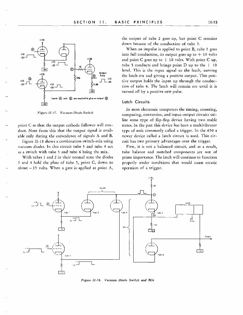
® +10 JL ·35
+150
+150
+10..JL.. ·35
SECTION II.
+150
lK © o-./Vv-+-
33K
3.6K
Oulput Pulse 11 +10
...J L .35
Inputs ® and ® are required to gTve an output @
Figure II-I 7. Vacuum Diode Switch
point C so that the output cathode follower will conduct. Note from this that the output signal is available only during the coincidence of signals A and B.
Figure II-IS shows a combination switch-mix using vacuum diodes. In this circuit tube 3 and tube 4 act as a switch with tube 5 and tube 6 being the mix.
With tubes 1 and 2 in their normal state the diodes 3 and 4 hold the plate of tube 5, point C, down to about - 35 volts. When a gate is applied at point A,
Switch
BASIC PRINCIPLES II·15
the output of tube 2 goes up, but point C remams down because of the conduction of tube 3.
When an impulse is applied to point B, tube 1 goes into full conduction, its output goes up to + 10 volts and point C goes up to + 10 volts. With point Cup, tube 5 conducts and brings point D up to the + 10
level. This is the input signal to the latch, turning the latch ON and giving a positive output. This positive output holds the input up through the conduction of tube 6. The latch will remain ON until it is turned off by a positive OFF pulse.
Latch Circuits
In most electronic computers the timing, counting, computing, conversion, and input-output circuits utilize some type of flip-flop device having two stable states. In the past this device has been a multivibrator type of unit commonly called a trigger. In the 650 a newer device called a latch circuit is used. This circuit has two primary advantages over the trigger.
First, it is not a balanced circuit, and as a result, tube balance and matched components are not of prime importance. The latch will continue to function properly under conditions that would cause erratic operation of a trigger .
• 70.
68
SL r--------<;r-----=--==---~©
lotch
-35'~
O ... tpul
.,0..----, 3\~ -50
L
Figure II-lB. Vacuum Diode Switch and Mix

II-16 IBM 650
ON INPUT
OFF CONTROL
3
IN-501
4 6
-50
Figure 1I-19.
Second, a latch is comprised of a double inverter and cathode follower, usually with a diode switch or mix input to the latch circuits. This permits standardizing on fewer types of pluggable units. When triggers are used, several different types are required. A latch is merely put together from existing inverter, cathode follower, and diode units.
Figure II-19 shows a latch circuit with a diode mix input. An input pulse will raise the grid of the first triode inverter above cutoff, causing the triode to conduct. This in turn lowers the grid potential of the second inverter below its cutoff point. The plate voltage rise of the second inverter in the non-conducting state causes the grid of the cathode follower to rise to a conducting potential. As a result the cathode follower output rises to about a + lO-volt potential.
This output is available for use, to act on some further circuit, and is fed back to the grid of the first inverter through the switch and mix diode circuitry to hold it at a conducting potential. This positive feedback is sufficient to hold the circuit in the latched condition. This ON condition will sustain itself until some external action is applied to the circuit to render
8
CF-.503
56--_ OUTPUT
Latch Circuit
the output cathode follower non-conductive. The most common method of turning a latch off is by lowering the signal on the latch back diode switch labeled OFF control.
When this signal goes down there is no longer a feed-back signal to keep the first inverter in a conducting status. Its plate voltage rises, causing the second grid to rise and throwing the second inverter into conduction. When this happens, its plate voltage goes down, thus forcing the output cathode follower signal to go down, thereby turning the latch off.
Another method of turning the latch off is to put in a positive signal to the second grid, pin 6. This causes the second inverter to go into conduction, bringing its plate voltage down, thus forcing the cathode follower output down.
When the latch is OFF it may be turned ON by a negative pulse applied to the second grid, pin 6. This negative pulse will turn the second inverter off, cause its plate voltage to go up, the cathode follower output to go up, and feed back to the grid of the first inverter and hold the latch ON.
The latch may also be turned on by clamping the

+150 04 03
OFF Input Signal
JL
SEC T 1-0 N I I .
02 01
ON Input Signal ..n..
+150
Figure lI-20. Double Latch Circuit
plate of the first inverter with another triode. This tube shares the same load resistor as the first inverter so that, when it conducts, the plate of the first inverter goes down and thus causes the latch to turn ON.
In a similar manner the latch may be turned OFF by clamping the plate of the second inverter down with another triode. When the plate of the second inverter is pulled down, the cathode follower output goes down and the latch is turned OFF.
It is also possible to reset the latch by connecting pin 4 to a reset line. If this reset line is allowed to go up, the bias will be removed from the second inverter, and it will go into conduction. When it conducts, its plate voltage goes down, the cathode follower output goes down, and the latch is reset OFF. This reset may be either automatic or controlled manually.
Figure II-20 shows a double latch circuit. This circuit is frequently used where the extra safety and checking action of a positive OFF signal is desirable. This circuit is comprised of two single inverters, two cathode followers with divider grid inputs and two diode mix circuits. Input variations can be obtained by using switch-mix diode circuitry instead of simple mixes as shown.
Initial circuit conditions, assuming the latch to be OFF are as follows:
BASIC PRINCIPLES II-l7
1. T1 conducting 2. A at low potential 3. B at no-signal level 4. C at no-signal level (- 35) 5. D below cutoff potential through mix diode D1 6. E at high potential 7. F at signal level (+ 10) 8. G at signal level (+ 10) 9. H at conducting potential through mIX diode
D4 holds T1 conducting.
When an ON input signal is applied to D through mix diode D2, the circuit is transferred to an opposite set of conditions. T2 conducts, lowering the output of T3, which drops H below cutoff potential. A rises and T 4 conducts, raising C, which holds D up through mix diode D 1. The latch has been turned on and remains in this condition until an OFF input signal restores it to the initial state.
Latch Ring
For timing and synchronizing purposes it is necessary to generate timed pulses and gates. These are used to establish the basic machine cycles and controlling gate voltages. A ring type of circuit is used to develop some of these timing gates. The latch cir:" cuit previously described is easily adapted for use in a ring circuit. Figure II-21 illustrates a 10-point ring where the first two stages and the last stage are shown together with a theoretical timing chart showing the relationship of input, output, and transfer pulses. The input pulse source is a cathode follower drive from a basic timing source such as permanently recorded spots on the drum timing tracks. The negative input pulses are about two microseconds in duration with an amplitude of 45 volts ranging from - 35 volts to + 10 volts. The cathode follower output gates have a duration equal to the time interval between the driving pulses with a swing of about - 40 to + 10 volts.
Assume that only stage 1 is on and thus the 1 output is at + 10 volts. This condition exists at time to of the timing chart. The + 10-volt 1 output signal through diode Y 1 of the diode switch in coincidence with the + 10-volt input signal through diode Xl of the same switch, holds the grid of the first inverter of stage 1 at conducting potential. This estab-
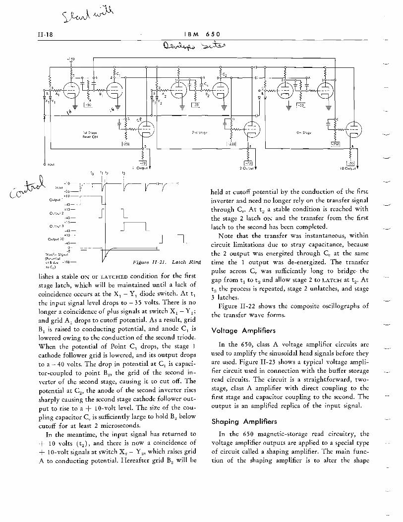
II-18 IBM 650
+150
'0 I I
+10-1 ---Input :/ J
-35-' +10-,--
Output 1 I -40- _J
'+10-Output 2
-40-+10-
Output 3
-40-+10-
Output 10 -40--0--3-
Transfer Signal (Potential at B due -100-to ee)
L J L
Figure I 1-21. Latch Ring
lishes a stable ON or LATCHED condition for the first stage latch, which will be maintained until a lack of coincidence occurs at the Xl - Y I diode switch. At tl the input signal level drops to - 35 volts. There is no longer a coincidence of plus signals at switch Xl - Y I;
and grid Al drops to cutoff potential. As a result, grid BI is raised to conducting potential, and anode C I is lowered owing to the conduction of the second triode. When the potential of Point C I drops, the stage I cathode follower grid is lowered, and its output drops to a - 40 volts. The drop in potential at C I is capacitor-coupled to point B2 , the grid of the second inverter of the second stage, causing it to cut off. The potential at C 2 , the anode of the second inverter rises sharply causing the second stage cathode follower output to rise to a + IO-volt level. The size of the coupling capacitor C e is sufficiently large to hold B2 below cutoff for at least 2 microseconds.
In the meantime, the input signal has returned to + IO volts (t2 ), and there is now a coincidence of + I o-volt signals at switch X 2 - Y 2' which raises grid A to conducting potential. Hereafter grid B2 will be
2 Output 10 Output
held at cutoff potential by the conduction of the first inverter and need no longer rely on the transfer signal through Ce. At t2 a stable condition is reached with the stage 2 latch ON and the transfer from the first latch to the second has been completed.
Note that the transfer was instantaneous, within circuit limitations due to stray capacitance, because the 2 output was energized through Ce at the same time the I output was de-energized. The transfer pulse across C e was sufficiently long to bridge· the
gap from tl to t2 and allow stage 2 to LATCH at t 2• At t3 the process is repeated, stage 2 unlatches, and stage 3 latches.
Figure 11-22 shows the composite oscillographs of the transfer wave forms.
Voltage Amplifiers
In the 650, class A voltage amplifier circuits are
used to amplify the sinusoidal head signals before they are used. Figure 11-23 shows a typical voltage amplifier circuit used in connection with the buffer storage read circuits. The circuit is a straightforward, twostage, class A amplifier with direct coupling to the first stage and capacitor coupling to the second. The output is an amplified replica of the input signal.
Shaping Amplifiers
In the 650 magnetic-storage read circuitry, the voltage amplifier outputs are applied to a special type of circuit called a shaping amplifier. The main function of the shaping amplifier is to alter the shape
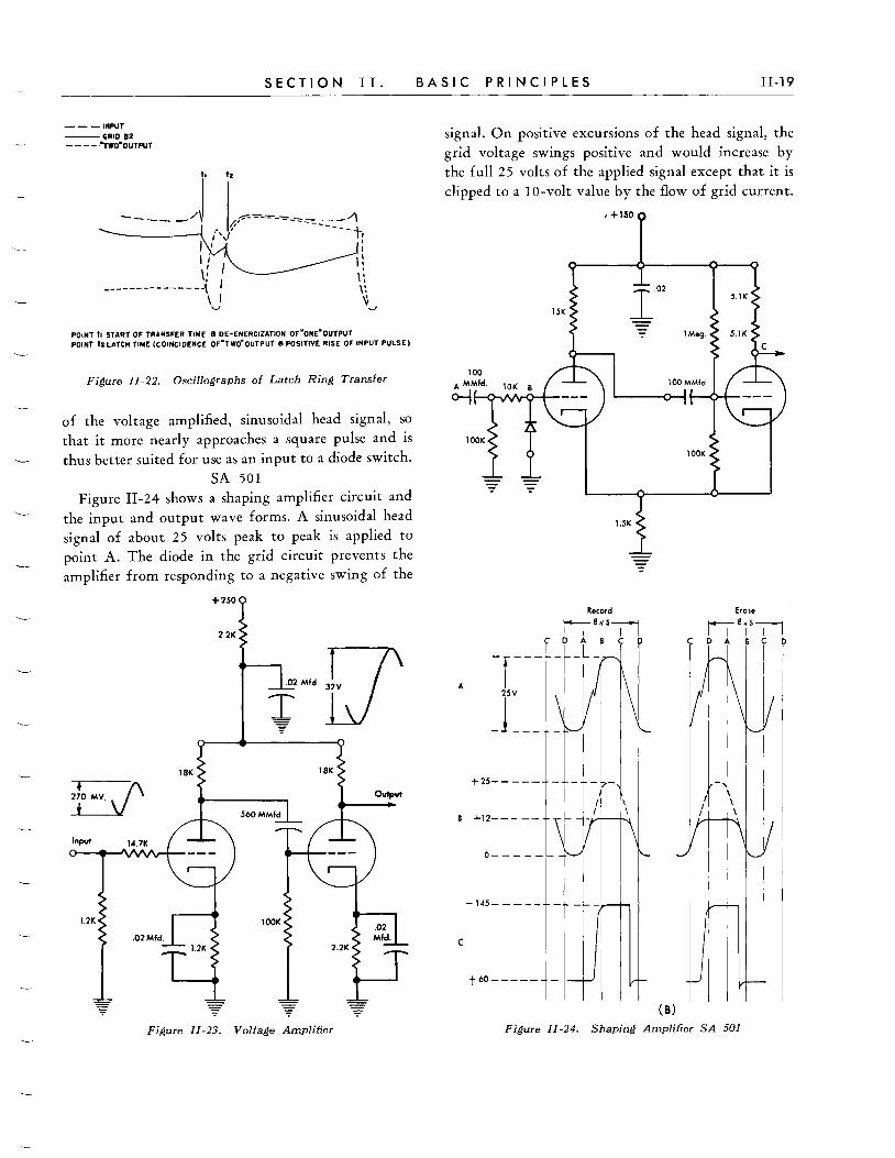
SECTION II.
---INPUT --GRID 82 - - - - ·"TWO·OUTPUT
;:?=-=---=---"'=-7 -/I /\',,( ---lOot
I I ,:
I I Il, I II I
\ : ---------------i ' \\ \ I ~
V V
POINT" START OF TRANSFER TIME a DE-ENERGIZATION OF·ONE·OUTPUT POINT fa LATCH TIME (COINCIDENCE OF"TWO"OUTPUT III POSITIVE RISE OF INPUT PULSE)
Figure II-22. Oscillographs of Latch Ring Transfer
of the voltage amplified, sinusoidal head signal, so that it more nearly approaches a square pulse and is thus better suited for use as an input to a diode switch.
SA 501 Figure II-24 shows a shaping amplifier circuit and
the input and output wave forms. A sinusoidal head signal of about 25 volts peak to peak is applied to point A. The diode in the grid circuit prevents the amplifier from responding to a negative swing of the
+2.50
2.2K
Inpvt 147K
1.2K
Figure II-23. Voltage Amplifier
BASIC PRINCIPLES II-19
signal. On positive excursions of the head signal, the grid voltage swings positive and would increase by the full 25 volts of the applied signal except that it is clipped to a 10-volt value by the flow of grid current.
A
i-25-- ---
B i"12-----
C
, +150
1°2
Record -8.S-:--l I I I I I DAB C
( B)
Erase
t--- 8,5-:--1 I I I I I
COABCO
/ 1\
Figure II-24. Shaping Amplifier SA 501

II-20 IBM 650
This clipping is shown by the dotted lines of the curves for point B. The output of the first stage is capacitor-coupled to the second stage, the output of which is shown by the curves for point C.
Thus, whenever the head signal swings in a positive direction, the shaping amplifier responds with a reasonably square pulse that IS m phase with the posi
tive signal swing. SA 506
Figure II-25 shows the input and the output wave forms and the shaping amplifier circuit used in general storage. The amplified head signal of about 25 volts peak to peak is applied to point A. Grid bias for TI is developed across RI on the negative swing of the input signal and holds TI cut off. On the next positive swing of the input signal, TI will conduct when the grid rises above cutoff. The grid rises to ground potential and is clamped at ground by the diode action of the grid and cathode as shown for point B. Wave form C shows the output of the first stage. This isinverted by the second stage to produce a positive square wave on each positive swing of the
A
c
D
-r---25V _1 ____ _
+50---
+150-----
F,·gure Il-25. Shaping Amplifier SA 506
head signal (Wave form D). As the amount of grid bias of TI is determined by the input signal, smaller head signals have less bias to overcome. Larger head signals must overcome a higher bias. This permits correct operation over a wider range of head signal amplitudes.
Power Units
A number of units are used in the 650 that are called power units. In general a power unit is basically either a cathode follower or an inverter using a tube type designed to deliver more power to the circuits that it drives.
One rather special type of power unit (PW502) is found in the magnetic-storage writing circuits. It is a two-stage unit consisting of an inverter, with a plate peaking inductor, and capacitor-coupled output cathode follower. The purpose of this unit is to develop an extremely sharp, short-duration signal for controlling the tube which impulses the write coils so that a short, sharp impulse of write current will be forced through the coil whenever a magnetic spot is to be placed on the drum surface.
Figure II-26 illustrates some typical power units found in the 650.
Figure II-27 illustrates the circuit and wave forms of the PW502 peaking power unit. In operation this unit is normally cut off and is pulsed by a twomicrosecond pulse as shown at A. This positive pulse causes T 1 to go into conduction, and the voltage at point B drops as shown by the curves. As current starts to flow through the peaking coil, the voltage at B rises along a time constant curve. At the end of the two-microsecond pulse, T 1 is cut off. This stops current flow and induces a large back emf in the peaking coil. This induced emf attempts to keep current flowing so that its potential is positive at point B. This accounts for the high positive spike of voltage at point B. This same wave shape is carried through the capacity-coupled cathode follower. It is this short-duration voltage spike that is used to operate the power unit that causes current to flow through the magnetic head to write on the drum.

56K
-150
A
270.n.
~. > ~~ " )
••••. J ...... . . , , . . , , . ~ ••••••••••• J
B
390K
Figure 11-26. Power Units 1I-21
68K
+ 150
c -50-
.-275--1
I ,
* >~
t :.~~-:
I _ ____ I
+ 120 --+--+."
+250-
D
+25--
Figure 11-27. Special Power Unit

II-n IBM 650
.. ."
-50
Not below -30
-30
Normally at -30 cannot get above ground
.,0------______ _
c ."0-----,.-\ Ir--~\--.-l ------<
·,,---rt-'------'I-, -'-----
Single-Shot Multivibrators
2k
2k
Several single-shot multi vibrators are used in the circuits for the development of constant-width square timing pulses from the sinusoidal-shaped signals obtained from the timing tracks. These units are built up by external circuitry applied to a basic PW504.
A typical single-shot multivibrator circuit is shown in Figure II-28, together with the wave forms at various points of the circuit. The input pulse is the cathode follower modified output of a shaping amplifier, part of the read circuitry associated with the heads, which read the permanently recorded spots of the timing tracks.
In this circuit the right-hand tube is normally conducting as indicated by the X in the tube schematic. The left-hand tube is held cutoff by the - 30-volt
2k
2k
+150
2k
S6k R 2k E 250 Mmfd
+70 +150
2k F .01 mfd G
2k
Figure II-28. Single-Shot Multivibrator
potential at point B, developed by the voltage divider action of the resistor-diode input circuitry. As the input pulse swings in a positive direction, point B tends to rise by the same amount but is clamped when it reaches ground (0 volts) by conduction of diode D3, which together with D2, prevents positive signal voltage variations from influencing the multivibrator during its ON time. This rise of point B causes Tl to conduct with the consequent drop in plate voltage as shown by the curves for point C. This negative voltage shift cuts off T 2' through the capacitor C b which together with R governs the ON time of the circuit and thus determines the width of the output pulse. As shown by the wave form for point D, T 2 remains cut off until D reaches cutoff along the capacitor charge curve as determined by the time constant R X C t (75mmf X 56K = 4.2 microseconds).
When T 2 cuts off, the positive voltage shift at its plate is applied to point B through the 250mmf capacitor, thus holding the multivibrator on until R X C t can cause it to turn off, even though the effect of the input signal is no longer felt at point B. This is why the curve at point B remains flat at 0 volts in-
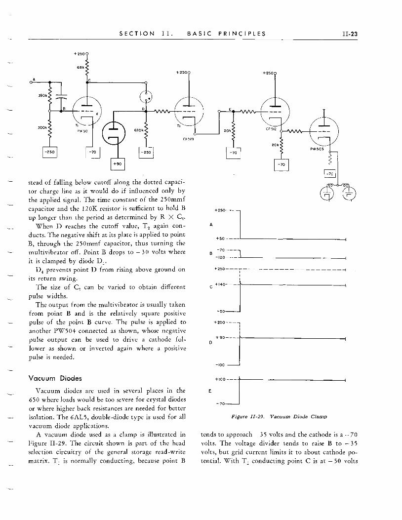
SEC T I· 0 N I I .
+250
68k +250
A
stead of falling below cutoff along the dotted capacitor charge line as it would do if influenced only by the applied signal. The time constant of the 250mmf capacitor and the 120K resistor is sufficient to hold B up longer than the period as determined by R X Cl"
When D reaches the cutoff value, T ~ again conducts. The negative shift at its plate is applied to point B, through the 250mmf capacitor, thus turning the multivibrator off. Point B drops to - 30 volts where
it is clamped by diode D 1. D4 prevents point D from rising above ground on
its return swing. The size of C t can be varied to obtain different
pulse widths. The output from the multivibrator is usually taken
from point B and is the relatively square positive pulse of the point B curve. The pulse is applied to another PW504 connected as shown, whose negative pulse output can be used to drive a cathode follower as shown or inverted again where a positive pulse is needed.
Vacuum Diodes
Vacuum diodes are used in several places in the 650 where loads would be too severe for crystal diodes or where higher back resistances are needed for better isolation. The 6AL5, double-diode type is used for all vacuum diode applications.
A vacuum diode used as a clamp is illustrated in Figure II-29. The circuit shown is part of the head selection circuitry of the general storage read-write matrix. T 1 is normally conducting, because point B
BASIC PRINCIPLES II-23
+250
E
, ~~:~~--------------------------~ B -70---\
-120--- ...... --------------_---l
+250---,-- - - -- ----_________ -j
I
+200---, I I
D +90J--I
-100
E +IOOJ-
-70
Figure 1I-29. Vacuum Diode Clamp
tends to approach - 35 volts and the cathode is a - 70 volts. The voltage divider tends to raise B to - 35 volts, but grid current limits it to about cathode potential. With T1 conducting point C is at - 50 volts

II-24 IBM 650
because about 300 volts is dropped across the 68K load resistor and about 20 volts across the tube. The voltage divider action of the 620K resistor and the neon bulb holds point D at -100 volts and T~ is cut off. (The neon bulb maintains a constant 50-volt drop across itself as long as it is conducting.) With T ~ cut off, point E is at - 70 volts.
When A drops to + 50 volts, the voltage divider allows B to drop to - 120 volts, cutting off T 1 • Point C tends to rise to + 250 volts. As Crises, D is pulled up at the same rate, but always 50 volts below C because of the action of the neon bulb. In this fashion D tends to rise to + 200 volts but is clamped at + 90 volts by the vacuum diode, which conducts at this point, effectively shunting the 620K resistor and changing the proportions of the voltage divider system. The heavier current due to the conduction of the diode causes a greater drop across the 68K load resistor, and point C never reaches + 250 volts but stops at + 140 volts.
The object here is to raise point D from its initial - 100-volt level to + 90 volts as rapidly as possible. To accomplish this, the large voltage swing of point C is used. The neon bulb provides 50-volt difference between points C and D and allows point D to vary between the desired limits while dropping some of the excess driving voltage. If a resistor were used in place of the neon bulb, of such a size as to allow point D to be at its initial - 100-volt level, so much voltage would be dropped across it when point C rises that D would never reach the desired + 90-volt level.
Vacuum diodes are also used in series with the magnetic-storage read and write coils in the general storage selection matrix to prevent back circuits between commonly connected points and in the basic capacitor storage cell from which the capacitor storage units are built up. These uses will be explained in more detail in connection with the specific circuits.
Capacitor Storage
Capacitor storage units are used in the 650 for working storage, where the information must be available frequently and rapidly, for calculating and control purposes. These capacitor storage units (accumulator, distributor, and program register) are built up from basic capacitor storage binary cells, each of
which is capable of storing one binary bit by virtue of its two possible states, charged and discharged.
One such capacitor storage device is shown in Figure II-30. The basic cell consists of diodes Dl and D~ and the storage capacitor Co> T l' T~, and T;: are shown to illustrate typical controlling circuits.
The initial circuit conditions are as follows: 1. C" discharged 2. T1 conducting at no-signal level; thus A IS at
- 35 volts 3. T2 cut off, thus B is at + 150 volts 4. T:I conducting at no-signal level; thus D is at
- 35 volts and, because there is no charge on C", point C is also at - 35 volts.
T 1 and T 2 are pulsed periodically by timing pulses from timing rings.
The pulsing of T 1 provides a positive read-out gate and is followed by the pulsing of T 2 which produces a negative read-in gate. T 3 is pulsed under control of the capacitor storage read-in circuitry (not shown) and is active only when it is desired to readin to the capacitor.
The capacitor is considered to be storing a binary 1 when it is discharged and a binary 0 when charged. Thus, reading into a capacitor storage cell requires that the capacitor be left discharged upon termination of the read-in gate.
The wave forms of Figure II-30 show how this is accomplished. When the read-out gate is applied, A rises to + 10 volts, causing Dl to conduct. This connects point C to point A and pulls C up to + 10 volts. This upward shift raises point D momentarily until the capacitor can charge and allow D to return to - 3 5 volts along the capacitor charge curve as determined by R X C s • This sharp pulse at D is obtained whenever the read-out gate tests a discharged capacitor. Had the capacitor been charged, no output pulse would appear. Termination of the read-out gate returns A to - 35 volts and effectively disconnects A and C, leaving C at + 10 volts. When the read-in gate is applied, B is lowered to + 10 volts, but with C also at + 10 volts there is no potential difference across D2 and no conduction occurs. No path is available to discharge CR' Under these conditions the capacitor remains charged upon termination of the read-in gate. A 1 has been read out, and a 0 has been stored.

+150
SECTION II.
8
+-----'''--_ ..... D _____ Output Pulse
Store "0" +IO--~ A A
A Reod out Gote -35
+150
Cycle Cycle Cycle 23 4
Reod out "I" Read out "0" Reod out "0" Store II]" Store "011 Store 11111 AAA AA~ AAA
Figure 11-30. Basic Capacitor Storage Device
Cycle 2 also assumes that C s is discharged when
tested by the read-out gate and an output pulse is obtained. Here, however, it is desired to st'ore a 1
and the capacitor must be left discharged. To accomplish this, the read-in control circuits (not shown)
cause the pedestal cathode follower (T 3) to conduct simultaneously with the read-in gate, This causes D
to be raised by an amount equal to the pedestal
pulse from the output of T 3' This positive shift at D is reflected momentarily through C s to point C. Thus
when B is lowered to + 10 volts by the read-in gate
C, which was at + 10 volts is simultaneously raised
to 55 volts by the pedestal pulse. Under these
conditions, D2 conducts, and C. discharges through
D2 and R while sitting on top of the pedestal. At the
termination of the pedestal pulse, points D and C are lowered to - 35 volts. The capacitor has been dis
charged during the read-in interval and a 1 is stored.
Cycles 3 and 4 show the action of the circuit un
der the other two possible conditions: read-out 0
and store 0, and read-out 0 and store 1.
BASIC PRINCIPLES II-25
Because a capacitor will not maintain a charge in
definitely, capacitor storage is a }lon-sustaining type of storage requiring periodic regeneration. In the 650
each capacitor has a read-out gate and a read-in gate applied to it once every word interval (96 micro
seconds) in the case of the distributor and program
register storages, and once every two word intervals (192 microseconds) in the case of the accumulator storage. When the capacitor storage unit is required
to read-out and retain its information for several
word intervals, each cell must be regenerated once each word. This is accomplished by causing the out
put pulse obtained when a 1 is read out, and that
is available several microseconds before read-in time, to actuate the read-in control circuits so that a pedestal pulse is obtained simultaneously with the read
in gate. Thus, when regenerating, any time a 1 is read out, a pedestal is obtained, and a 1 is read back into
the same capacitor. If a 0 is read out, no output
pulse is available to actuate the read-in control cir
cuits, no pedestal is obtained and a 0 is read back in.
Cycles 2 and :) illustrate the two possible conditions
during regeneration.
When it is desired to read a new word into a capacitor storage unit, the path between the output pulse
and the read-in control circuits is blocked, and the
read-in controls, and consequently the pedestal cathode followers, are actuated by information pulses from the read-in source.
A later section will describe how several capacitor storage cells are combined and controlled to form a
bi-quinary, serial storage unit capable of storing the
digits of one or two words.
GERMANIUM CRYSTAL DIODES
THE germanium crystal diodes used in the 650 are
supplied by two different vendors. They are similar
electrically. The physical construction and polarity
markings are shown in Figure II-31. An additional
marking in the form of a painted red dot may be
found on the anode end.

II-26
Metal Clip Terminals Cathode End Gold Color
Germanium Crystal
IBM
Glass Metal Clip Terminal (Anode)
Plastic Sleeve
Figure Il-31. Germanium Crystal Diodes
These diodes are sealed in glass to protect against moisture and temperature variations. The characteristics, however, are greatly affected by the operating temperature. In general, the front-to-back current or resistance ratio decreases as temperature increases, thus decreasing the diodes' effectiveness. At about 100 degrees c., germanium no longer exhibits semiconductor characteristics, and a temperature in excess of about 150 degrees C. will permanently alter its behavior. For this reason the pluggable diode units are mounted in vertical rows on each chassis, and cooling air is circulated by blowers at the top and bottom of each gate.
These diodes are especially manufactured for computer use. They have a minimum back resistance of about 400K and a maximum forward resistance of about 200 ohms, under operating conditions. Attention is also given to forward and reverse recovery
times when diodes are used in pulsed circuits.
PLUGGABLE UNITS
As IN previous IBM calculators, functional units are built in pluggable unit assemblies. The pluggable units use miniature ten-pin basis, which plug into wired
sockets mounted on chassis.
650
In the console unit there are three gates of three chassis each, and in the power unit there is one gate mounting two chassis. On machines manufactured after February, 1956, the power unit contains a maximum of two gates of three chassis each. One of the chassis consists of relays. There is also a small relay gate mounted above the cable connectors on the end of the power unit. Pluggable units are located on the chassis by columns A through Z (except 0 and I) <lnd rows 1 through 11 as in previous electronic calculators.
All tubes are part of pluggable units. Units are named according to function. Inverter units are identified with an IN prefix such as IN501, IN503, etc. Cathode followers, power units, voltage amplifiers, shaping amplifiers, thyratrons, double vacuum diode units, and capacitor storage units are similarly identified with the prefixes CF, PW, VA, SA, TH, DD, and CS respectively.
Several types of CF, IN and PW units are provided. Use of a particular type depends on the circuit requirements. An inverter unit may serve as two separate single inverters or its sections may be combined to act as a double inverter. Examples of these are the IN503 and the IN501.
Several types of cathode follower units provide different load resistance values, various types of grid divider, and input arrangements, etc. Many cathode follower units, such as the CF501 and the CF502 are duplicates except for the use of the 6350 tube instead of the 5965 to provide more drive.
Germanium crystal diode switch and mix circuits
are also built up in pluggable units. In the 650, up to twelve diodes are mounted in a pluggable unit. The associated resistors used in the switch or mix circuits are connected externally. The diodes are clipped into the units, allowing easy replacement of individual diodes without need of soldering. With this arrangement, one pluggable diode unit may comprise several logical switch or mix functions.
The logical circuits have been formed using various configurations of the pluggable diode units. Each pluggable diode unit frame is the same, including the wiring between pins and diode clips, and each has the same part number. The several configurations are determined by the number of diodes used, their position within the unit, and the direction in which they are clipped into the unit.

SECTION II.
The basic configuration, with all diodes clipped in the forward direction, is shown in WD 00-05. A diode chart in the wiring diagram, in chassis location order, lists the diodes used in their direction.
All pluggable unit schematic and point-to-point diagrams, together with the representative block diagram of the unit, ar shown in the wiring diagram.
Two types of pluggable units containing only capacitors are used as voltage supply filters on chassis 6. These units are named according to the size and working voltage rating of the capacitors that they contain; i.e., C-30-30-150 and C-20-450 (WD 00-16).
BLOCK SYMBOLS
To SIMPLIFY the logical representation of circuits, a system of block diagrams is used. Each block symbol represents a basic function. An effort has been made to identify the functional classification of a unit by the configurations of its block symbol. The physical location of the unit represented is shown over the block, and the unit-type identification, as well as the pin numbers, is shown for cross-referencing to the detailed pluggable unit drawings.
WD 00-07 through 00-16 and 00-30 show the block symbols that are used for 650 circuit representation. The most common tube functions are single inverters and cathode followers, both single-triode functions. These are shown as a square block with grid input on the left and anode or cathode output from top or bottom as the case may be. In each case these are half of a pluggable unit. When both halves of a unit are used for a single function, as in double inverters, the block is a rectangle with twice the area of a half unit. Double diode pluggable units contain two, double vacuum diode tubes (6AL5's), or four diode functions. Thus, a DD functional block is a rectangle, one half the area of a half unit block.
A single latch is made of a double inverter and a cathode follower (WD 00-30). Connections between the inverter output anode and the cathode follower grid need not be included every time a latch symbol appears. Thus, a latch symbol is an IN rectangle and a CF square joined as shown. Similarly, a double latch is an inverter plus two cathode followers, one on each side. Where latch input circuitry utilizes diode
BASIC PRINCIPLES II-27
switches and/or mixes, these will be shown as separate diode blocks. These distinctive latch configurations will help to locate latches on the wiring diagram. This is an advantage because latches are usually key components of a logical circuit.
On latch symbols grid inputs are shown entering the block from the bottom (left or right) instead of the left side as on other tube symbols in order to make room for the adjoining cathode followers.
In all other cases grid inputs are straight in from the left if there is no grid voltage divider network built into the unit. When a divider is a part of the unit, the grid input terminal is shown above the grid level as in the CF503.
Block Symbol Voltage Codes
When a unit has a built-in load resistor, this is indicated by a small box in the lower left corner of the block if it is a cathode follower, or the upper left corner if it is an inverter. If the load resistor is used, as is usually the case, the number in the box is the code number for the service voltage to which the load resistor is connected. These voltage codes are shown in WD 00-04.
Special input circuitry such as capacitors and diode clamps are shown as in the CF509, CF513, and CF516. Where a cathode load resistor for a preceding stage, which contains no built-in resistor of its own, is in the input of the next stage, it is shown as in the CF512. Here the cathode terminal of one-half of a CF512 may be connected directly to the grid terminal of the other half by wiring pin 5 to 6 or 3 to 8, thus
obtaining successive cathode follower stages. Input and output pin numbers are shown adjacent
to the terminal. In general, in the case of cathode followers and inverters, pins 3 and 5 are associated with the input and output terminals respectively, of one half of a unit while pins 6 and 8 are associated with the other half. In this way the pin numbers also serve to identify the unit half represented by a block.
In some cases where it is helpful to know that a tube element connects to an unusual voltage, this is shown. An example is the cathode of an IN505 which connects to - 22 volts rather than ground.
One pluggable capacitor storage unit contains two capacitor storage cells (two 6AL5's and two capacitors). These are shown as two separate functional

II-28 IBM 650
blocks with the same chassis location. Pins 3 and 4 are read-out gate terminals, 8 and 7 are read-in gate terminals while 6 and 10 are output pulse and pedestal input terminals.
In general, power units are shown as a block representative of their basic function as either an inverter or cathode follower. Special power units like the PW502 and PW503 have their own special block representation.
Voltage amplifiers and shaping amplifiers are actually special types of double inverters.
Thyratrons are the one departure from the basic system of using a full-size rectangle for a full pluggable-unit function. This was done to conserve wiring diagram space, because thyratrons are arranged in a matrix. In this block grid 1 and 2 inputs are from the left, cathode is at the bottom, and anode at the top.
A crystal diode pluggable unit may comprise severallogical switch and/or mix functions. For this reason the block representation uses several blocks with the same chassis location. Each switch or mix function contained in a pluggable unit is shown as a separate switch or mix block.
To distinguish crystal diode functions from tubes, the shape and size of the blocks have been made distinctive. Further to distinguish between a diode switch function and a diode mix function, the blocks are shown in distinctive positions. The switch (AND circuit) is shown as a long, low block with inputs to the bottom and output from the top. The mix (OR
circuit) is shown as a narrow, high block with in puts to the left side and output from the top. This same block proportion is carried into the higher level diagrams.
TIMING PULSES AND GATES
Basic Recorded Pulses
Information is recorded in the buffer storages and general storage by switching information gates with timing pulses to produce a specifically timed information pulse for energizing the writing heads.
Information is read from magnetic storage by switching a shaped, read head signal with a timing pulse to produce a specifically timed information pulse
A
8 ABC D A
I IDigi~~n~.rv~1 I
I I
6p.s
I Informolion Gol. I
A I
B
c
Figure Il-32.
Write Sample Timing Puise
TImed Output Pulse when information IS present at point A. Energizes Writing Head and thus determines position on Drum surface of written spa"
Principle of Magnetic-Storage Writing
that can be used to turn on a latch whose output will be an information gate similar in duration and timing to the one originally used in recording the spot.
Figures II-32 and II-33 illustrate these principles of magnetic-storage writing and reading.
A capacitor storage unit (distributor), whose output pulses are in the form of information gates, is frequently the source of information thus recorded in general storage. Also, capacitor storage units (distributor or program register) whose input circuits will respond to information gates, are frequently the destination of such information read from general storage.
Notice that the timing pulses occur at about the mid-point of the information gate interval when writing, and at the middle of the shaper output interval when reading.
Thus timing pulses determine the position of a spot when it is placed on the drum and also insure that information read from the drum is available in the form of a properly timed information gate. In a similar way, other necessary drum timing divisions are established by timing pulses such that the exact position of the drum is known by the computing and control circuits at all times.

BJ.s
A
B 1--1----'
CI--I---J
OH---......
EH---......I
SEC T 1·0 N I I .
3* I, _LillJ_2 2---J \fl-SASOI
Ampli I ied Head Signal
ShaPing AmpUI,er Output
CF Output }
'-----+---1 Read Sample Timing Pulse
I..-_-!-_-I Switch Output to lurn on Lotch
BASIC PRINCIPLES
o
InpulS to Diode Switch
01---.....1
o u
Buffer Storoge
11-29
F
FH---....J (Inlormalion Gate)
'------i Latch Oulput
Gf- ...----l Negative Lalch Reset Pulse Res.lslatch by remov i no coincidence of plus sionois Irom latch back diode switch.
Figure IJ-33. Principle of Magnetic-Storage Reading
Figure 1-8 shows the principal drum timing divisions. All drum times are with relation to HOME position, which is the beginning of sector o. Other drum divisions are sectors (5 per drum revolution), words (50 per drum revolution), digits (600 per revolution), and A, B, C, and D pulse, one of each per digit or 600 per drum revolution.
The basic timing interval is the eight microsecond digit interval, of which there are 600 around the cir-
cumference of the drum. Each digit interval is divided into four equal pulse intervals, A, B, C, and D. The beginning of a digit timing interval is marked by the leading edge of its A pulse. The B, C, and D pulses of a digit follow at two microsecond intervals. Twelve-digit intervals, each with its A, B, C, and D pulses are included in a work interval. The twelve digits of each word are successively, DX, DO, DI, D2, D3, D4, D5, D6, D7, D8, D9, DIO. DX is used
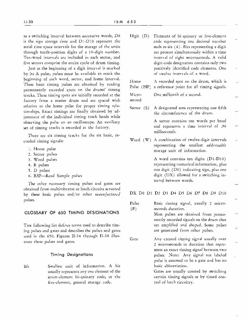
II-3~ IBM 650
as a switching interval between successive words, DO is the sign storage time and DI-DI0 represent the serial time space intervals for the storage of the units through tenth-position digits of a 10-digit number. Ten-word intervals are included in each sector, and five sectors comprise the entire cycle of drum timing.
Just as the beginning of a digit interval is marked by its A pulse, pulses must be available to mark the beginning of each word, sector, and home interval. These basic timing pulses are obtained by reading permanently recorded spots on the drums' timing tracks. These timing spots are initially recorded at the factory from a master drum and are spaced with relation to the home pulse for proper timing relationships. Exact timings are finally obtained by adjustment of the individual timing track heads while observing the pulse on an oscilloscope. An auxiliary set of timing tracks is recorded at the factory.
There are six timing tracks for the six basic, re-
corded timing signals:
1. Home pulse 2. Sector pulses 3 . Word pulses 4. B pulses 5. D pulses 6. RSP-Read Sample pulses
The other necessary timing pulses and gates are obtained from multivibrator or latch circuits actuated by these basic pulses and/or other manufactured
pulses.
GLOSSARY OF 650 TIMING DESIGNATIONS
THE following list defines terms used to describe timing pulses and gates and describes the pulses and gates used in the 650. Figures II-34 through II-3 S illus
trate these pulses and gates.
Bit
Timing Designations
Smallest unit of information. A bit usually represents anyone element of the seven-element bi-quinary code, or the five-element, general storage code.
Digit (D) Elements of bi-quinary or five-element code representing one decimal number such as six (6). Bits representing a digit are present simultaneously within a time interval of eight microseconds. A valid digit-code designation contains only two positively identified code elements. One of twelve intervals of a word.
Home A recorded spot on the drum, which is Pulse (HP) a reference point for all timing signals.
Microsecond
One millionth of a second.
Sector (S) A designated area representing one fifth the circumference of the drum.
A sector contains ten words per band and represents a time interval of .96 milliseconds.
Word (W) A combination of twelve-digit intervals representing the smallest addressable storage unit of information.
A word contains ten digits (DI-DI0) representing numerical information, .plus one digit (DO) indicating sign, plus one digit (DX) allowed for a switching interval between words.
DX DO Dl D2 D3 D4 D5 D6 D7 Ds D9 DI0
Pulse
(P)
Gate
Basic timing signal, usually 2 mIcroseconds duration. Most pulses are obtained from permanently recorded signals on the drum that are amplified and shaped. Some pulses are generated from other pulses.
Any created timing signal usually over 2 microseconds in duration that represents an exact timing signal between two pulses. Note: Any signal not labeled pulse is assumed to be a gate and has no basic abbreviation. Gates are usually created by switching certain timing signals or by timed control of latch circuitry.

SECTI.ON II.
Timing Designations with Abbreviations
a Timing divisions of a digit.
b One Digit -----'> I
c I
I I I I d a b c d a b
AP Basic 2 microsecond pulses within each digit.
I +-( ---- One Digit
CP
BP ) I
I DP AP BP CP DP I AP
41 2 micro. I <t:-seconds
Six hundred pulses per drum revolution, 8 mIcro
seconds apart.
A Pulse (AP). A positive pulse, 2 microseconds duration, occurring during the first quarter of a digit interval. A pulses are produced from a one-shot multivibrator, which is controlled by the leading edge of a delayed early A pulse and the leading edge of a nega
tive B pulse.
B Pulse (BP). A positive pulse, 2 microseconds duration, occurring during the second quarter of a digit interval. B pulses are obtained from permanently recorded signals on the magnetic drum.
C Pulse (CP). A positive pulse, 2 microseconds in duration, occurring during the third quarter of a digit interval. C pulses are produced from a one-shot multivibrator controlled by the trailing edge of a negative B pulse and the leading edge of a negative D
pulse.
D Pulse (DP). A positive pulse, 2 microseconds in duration, occurring during the fourth quarter of a digit interval. D pulses are obtained from permanently recorded signals on the magnetic drum.
Pulses that occur just prior (less than 2 microseconds) to a designated pulse time are signified with a prefix E meaning early. Early pulses are often used to compensate for time lost between stages of electronic circuitry that require an output at a certain
designated pulse time.
BASIC PRINCIPLES II-31
Early A Pulse (EAP). A positive pulse, 2 microseconds in duration, designed to occur about Yz microsecond prior to an A pulse. Early A pulses are obtained by delaying D pulses. Six hundred pulses per drum revolution, 8 microseconds apart.
Early Word Pulse (EWP). A positive pulse, 2
microseconds in duration, which occurs at early A pulse time every twelfth digit. Early word pulses are obtained from permanently recorded signals on the magnetic drum and are associated with DX, the first digit time of every word. Fifty pulses per drum revolution, 96 microseconds apart.
Early Sector Pulse (ESP). A positive pulse, 2 microseconds in duration, which occurs at early A pulse time every one-hundred-twentieth digit (or every tenth word). Early sector pulses are obtained from permanently recorded signals on the magnetic drum and are associated with DX, word 0, the first digit of the first word of every sector. Five pulses per drum revolution, 960 microseconds apart.
Early Home Pulse (EHP). A positive pulse, 2 microseconds in duration, which occurs at early A pulse time once every drum revolution. Early home pulse is obtained from a permanently recorded signal on the magnetic drum. Early home pulse is associated with DX, word 0, sector 0, the first digit of the first word of the first sector. One pulse per drum revolution, 4.8 milliseconds apart.
Home Pulse (HP ); Word Pulse (WP). These pulses, 2 microseconds in duration, are obtained by delaying their respective early pulse about Yz microsecond so that these pulses occur at A pulse time.
Word Pulse (Even Word); WPL (EvW). A positive word pulse, 2 microseconds in duration, which occurs for only every even word (192 microseconds apart). Words 0, 2,4, 6, 8 are considered even words and are associated with lower accumulator read-out
time.
Word Pulse (Odd Word); WPU (OdW). A positive word pulse, 2 microseconds in duration which occurs for only every odd word (192 microseconds apart) . Words 1, 3, 5, 7, 9 are considered odd words and are associated with upper accumulator read-out time.
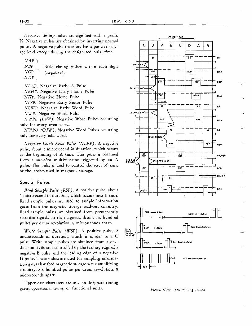
II-32 IBM 650
Negative timing pulses are signified with a prefix N. Negative pulses are obtained by inverting normal pulses. A negative pulse therefore has a positive voltage level except during the designated pulse time.
NAP f NBP NCP
NDPJ
Basic tlmmg pulses within each digit
(negative) .
NEAP. Negative Early A Pulse NEHP. Negative Early Home Pulse NHP. Negative Home Pulse NESP. Negative Early Sector Pulse
NEWP: Negative Early Word Pulse NWP. Negative Word Pulse NWPL (EvW). Negative Word Pulses occurnng
only for every even word. NWPU (OdW). Negative Word Pulses occurring
only for every odd word.
Negative Latch Reset Pulse (NLRP). A negative pulse, about 1 microsecond in duration, which occurs at the beginning of A time. This pulse is obtained from a one-shot multivibrator triggered by an A pulse. This pulse is used to control the reset of some of the latches used in magnetic storage.
Special Pulses
Read Sample Pulse (RSP). A positive pulse, about 1 microsecond in duration, which occurs near B time. Read sample pulses are used to sample information gates from the magnetic storage read-out circuitry. Read sample pulses are obtained from permanently recorded signals on the magnetic drum. Six hundred pulses per drum revolution, 8 microseconds apart.
-
° RUM
-
-
DElA .EO
-
OElA YEO
END NEG 'B' PU\.SE
Drum Signal Switched Wjth EAP'
-
-.-
--
--
~
-
fool ._---:;00.::..' :;;;Di'i'-..:!·J.:":·~_.--II
c 0 A B C 0 A B
- ----- -- -.- --- --- -- -DP OP OP
SIG(
---- -- ---- -- -- -NDP NDP NOP ......
~ -
~ --- .'---f ~- -- - EAP
'op'-< --c ~- -----1 5 -I l-tJ.. c.--- -- -
NEAP
AP AP AP
EAP'-k ~ -.- --- t\ ---- -
NAP NAP
I------ ~ ---- f---- -
NAP
BP BP BP
NAl(
-! RUM SI
-- -- -- --- - --- -- :::! NBP NBP NBP
f---- I---'::=-:-::' --- -- ---f-- --- --- ---CP CP
WSP WSP CP,WSP
>NE '0' PUL E
- -- -- --- -- -- -------NCP NCP NCP,
'--- "--
-- -.. ::. J= 17:1- ----lj- --~- NLRP
--- -- EF ------Ft -DRUM SI ...... Ij..
-I RSP
IporO,uOI,,,.luti.. * ,~L.
-R-5 per Orum f.volutiOft
'-------/-1-1 ----il J ~
'------i~" Drum " •• , •• i.o
600 D" Drum ,,",volulion
Write Sample Pulse (WSP). A positive pulse, 2
microseconds in duration, which is similar to a C pulse. Write sample pulses are obtained from a oneshot multivibrator controlled by the trailing edge of a negative B pulse and the leading edge of a negative D pulse. These pulses are used for sampling information gates that feed magnetic storage write amplifying circuitry. Six hundred pulses per drum revolution, 8
microseconds apart.
4 B/<. I--
Upper case characters are used to designate timing gates, operational terms, or functional units. Figure Il-34. 650 Timing Pulses
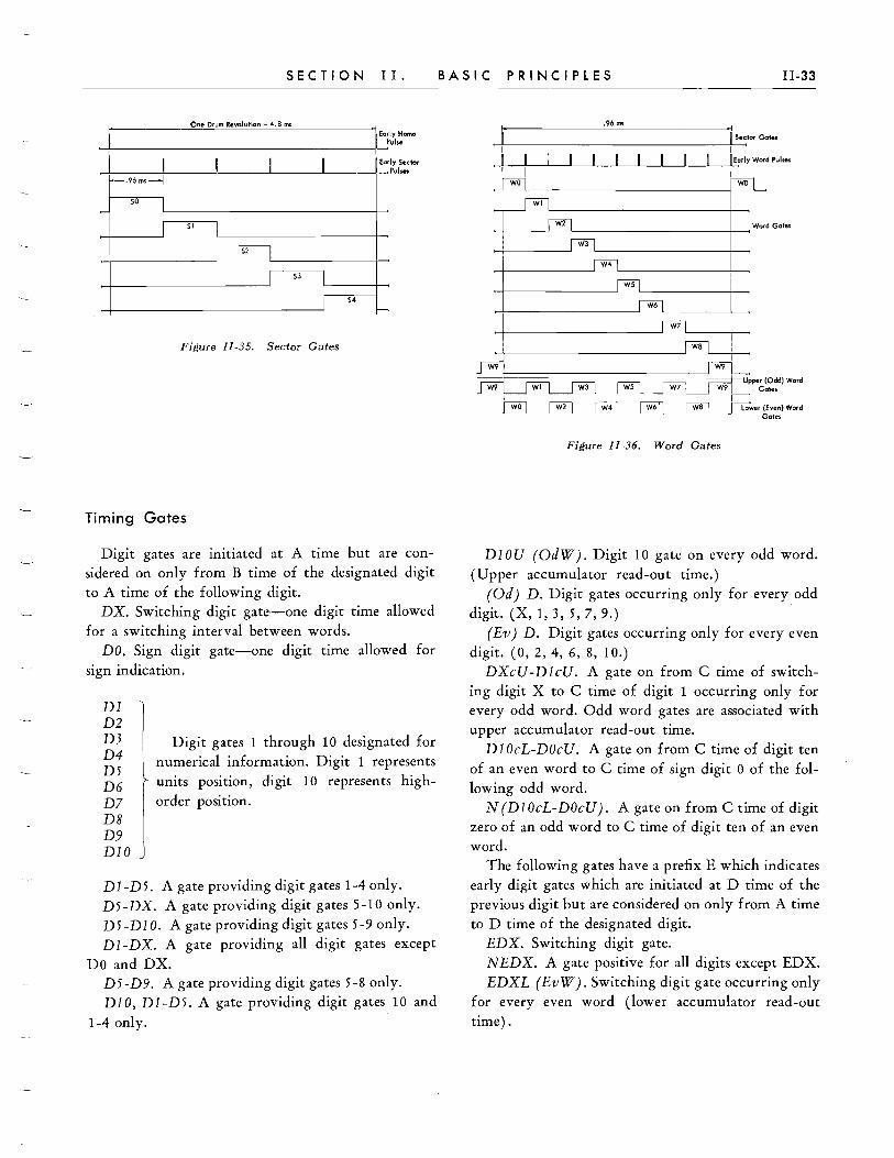
SECTION II.
One Drum Revolution - 4.8 ms • Early Home I Pulse
~------------------------------~I~
i Early Sector Pvlsa
-.96m.--j
50 I ~
I 51 I
I 52 I
I 53 I
I 54
r---
Figure II-35. Sector Gates
Timing Gates
Digit gates are initiated at A time but are considered on only from B time of the designated digit to A time of the following digit.
DX. Switching digit gate-one digit time allowed for a switching interval between words.
DO. Sign digit gate-one digit time allowed for sign indication.
DI 1 D2 D3 D4 D5 D6 D7 D8 D9 DIO
Digit gates 1 through 10 designated for numerical information. Digit 1 represents units position, digit 10 represents highorder position.
DI-D5. A gate providing digit gates 1-4 only. D5-DX. A gate providing digit gates 5-10 only. D5-DIO. A gate providing digit gates 5-9 only. DI-DX. A gate providing all digit gates except
DO and DX. D5-D9. A gate providing digit gates 5-8 only. D 10, D 1 -D 5. A gate providing digit gates 10 and
1-4 only.
BASIC PRINCIPLES 11-33
.96m$
, Sector Go ...
>-+----------------------~·f-~E.-rl~ word Pulses
-r~--~-L~~~~L~L-J-~-~I
L-___________________ ~~
L---------------t--< Word Gate.
Figure II-36. Word Gates
DIOU (OdW). Digit 10 gate on every odd word. (Upper accumulator read-out time.)
(Od) D. Digit gates occurring only for every odd digit. (X, 1,3,5,7,9.) .
(Ev) D. Digit gates occurring only for every even digit. (0,2,4, 6, 8, 10.)
DXcU-DIcU. A gate on from C time of switching digit X to C time of digit 1 occurring only for every odd word. Odd word gates are associated with upper accumulator read-out time.
DIOcL-DOcU. A gate on from C time of digit ten of an even word to C time of sign digit 0 of the following odd word.
N(DIOcL-DOcU). A gate on from C time of digit zero of an odd word to C time of digit ten of an even word.
The following gates have a prefix E which indicates early digit gates which are initiated at D time of the previous digit but are considered on only from A time to D time of the designated digit.
EDX. Switching digit gate. NEDX. A gate positive for all digits except EDX. EDXL (Ev W). Switching digit gate occurring only
for every even word (lower accumulator read-out time) .
One Word - 96j...s
DIGIT GATES
EARLY DIGIT GATES
EDX
A-C GATE
Figure IJ-37. Digit Gates
II-34

H H
W 01
LOWER EVEN WORO
05-DX GATE
05-010 GATE
05-09 GATE
OXUC(Od W)- OIUCIOdWl GATE
OIOLCIEvWl-OOUCIDdWl GATE
010 LC lEv W) - OOUC lad Wl NEG. GATE
EDXUIOd Wl GATE
EOOU lad Wl GATE
EDIU(Od Wl GATE
EDOL IEvWl GATE
010 UIOd Wl GATE
EDXLtEv W) GATE
EO I L lEv WI GATE
Figure 11-38. Special Gates

II-36 IBM 650
EDXU (OdW). Switching digit gate occurring only for every odd word (upper accumulator readout time).
NEDXL (EvW). A gate positive at all times except EDX of even words (lower accumulator readout time).
NEDXU (OdW). A gate positive at all times except EDX of odd words (upper accumulator readout time).
EDO. Sign digit gate. NEDO. A gate positive for all digits except EDO. EDOL (EvW). Sign digit gate occurring only for
every even word (lower accumulator read-out time). EDO U (OdW). Sign digit gate occurring only for
every odd word (upper accumulator read-out time). EDI. Digit one gate. NEDl. A gate positive for all digit times except
ED 1. EDIL (EvW). Digit 1 gate occurring only for
every even word (lower accumulator read-out time). ED 1 U (OdW). Digit 1 gate occurring only every
odd word (upper accumulator read-out time). ED2. Digit 2 gate. NED2. A gate positive for all digits except ED2. ED2L (EvW). Digit 2 gate occurring only for
every even word (lower accumulator read-out time).
Sector gates are considered on from B time of digit X, word 0 to A time of the following digit X, word 0 (ten words).
so. SI. S2. S3. S4.
Sector Gates 0-4. Positive signals from a ring lasting approximately 960 microseconds. These gates distinguish one of five drum sectors.
Word gates are considered on from B time of digit X to A time of the following digit X (twelve digits).
WOo WI. W2. W3. W4. W5. W6. W7. WB. W9.
Word Gates 0-9. Positive signals lasting 96 microseconds. These gates establish the position of a word in a sector.
WL (EvW). Word gates occurring only for every even word (0, 2, 4, 6, 8; lower accumulator readout time).
WU (OdW) . Word gates occurring only for every odd word (1, 3, 5, 7, 9; upper accumulator read-out time) .
A-G. Timing gate on from A to C time within
each digit (equivalent of AP + BP). C-A. Timing gate on from C to A time within
each digit (equivalent of CP + DP). Figures II-39 through II-49 illustrate typical cir
cuitry used to obtain timing pulses and gates. In these circuits, extensive and flexible use is made of the single-shot multi vibrator circuit of Figure II-28. This is explained in the section on basic electronic circuits. The curves of voltage wave forms at key points of the circuits show how the desired pulse is obtained.
The sector, word, and digit gates illustrated in Figures II-3 5, II-36, and II-37 are developed by latch ring circuits as shown in Figure II-49. Figure II-50
illustrates the timing for a digit ring. The wiring diagram sections on timing circuits
show the details of the development of all timing pulses and gates.
These circuits can be found on wiring diagrarp sections 1-00, 1-10, and 1-20. Sections 1-30, 1-33, and 1-34 show the circuits of the sector ring, word ring, and digit ring, respectively.
PRINCIPLES OF MAGNETIC-DRUM STORAGE
THE 650 utilizes a revolving magnetic drum for stor
ing information in the form of small magnetized spots on its surface. This system of storage offers a large storage capacity in small space together with reasonably fast access.
It is well known that a current through a coil around a bar of magnetic material will induce the bar to become a magnet having a north and south pole at either end (Figure II-51). Which end becomes the north pole is dependent upon the direction of the current in the coil. This magnet has associated with it a magnetic field, the approximate distribution of which is shown by the dotted lines of Figure II-51. This field exerts a magnetizing force on materials placed in it.

A ~[-'O SIGNal 220' lZO MY
" ,IIPurl[D HEaD SIGNAL lOll
C SHapINIj All., OUTPUT
o CF OuTPuT ~ INPUT TO S S MULTIVIBAATQR
1ST GRID or SS M\I, (INPUT TO P .... ~O. INVERTER)
aNODE O~ INVERTfR
GRID or Cr
CATHODE OF' cr (NEGATIVE TIMING PULSE)
ANODE OF INVERTER
GRID OF CF
CATHODE Or CF POSITIVE TIMING PULSE
T'O h -,o~ \,-
T1'h -45~ \-
SEC· T ION I I . BASIC PRINCIPLES
~---------------------,
1 I 1 1 I 1 I I I I I 1 I
s 5 MUL flVIBR.6TOR I
- - - - - - - - - - - - - - - - - - - - __ I
Il-37
Figure JI-39. Circuit for Development of Negative and Positive Timing Pulses from Recorded Timing Track Signals. Typical of BP, NBP; DP, NDP
Suppose now a sheet of suitable magnetic material is placed near the electromagnet (Figure II-52). Some of the field of the magnet will pass through the sheet. In fact, there will be a greater concentration of field in the sheet than in the surrounding air because the magnetic material of the sheet presents less reluctance than air. (Reluctance in connection with a magnetic circuit is analogous to resistance in an electrical circuit). During the time that current is flowing in the coil, that part of the sheet through which the field passes will itself become a magnet.
If the proper material is used, some of this induced magnetism will remain in the sheet after current ceases to flow. The fact that current was made to flow in the coil has been recorded in the sheet, and this fact could be detected by passing a compass needle over the sheet. The polarity of the recorded spot would indicate the direction of flow of the current through the coil. This is the principle of magnetic storage.
k~':'D :,RCUIT C" 0,jTDJT 11,>PJ T TO SS t,1y )
'~T (,!'iID 0' So. ~J
G~IO 0" 5') ""y
TO PW ~O" '''''ERIER)
CliTHOOE 0' C~ ~02·
POSIT,,/( TIMING PU~ 5E
.'\ I-t 75 ',_.J
- ~O ----
", n I '
- 45 __ j ~-_
---~----------- ------, -- .. _- ------, I
I ~ I
S S Mil
I I 1
1
Figure II-40. Development of Positive Timing Pulse from Timing Track Signal when Similar Negative Pulse Is Not Required. Typical of Read Sample Pulse.
P051TUE TRlIlLING EOGE
T,)R'fS 55"'11 "ON"
NEGATI.E L.EAOING EOGE
TuRNS 55 MY "OFF" ~ ---11--·
DOTlED LINE SHOWS MOW GRID WOULD ACT IF CONTROLLED ONLY ey A ~ C! WITHOuT' on"TlMING
__ PUL.SE Ct:S LARGER IN THIS CIRCUIT THAN IN OTHER 55 MY WK[R[ R x CI IS SOLE CONTROL ON WIOTH OF PULSE It
I -----
Figure II-41. Development of Negative and Positive Timing Pulses from Established Timing Pulses. Typical of C Pulses from Band D Pulses
II-3S
-.~ ---i POSIT!\f( TIMIN(, Ptll Sf
-----1 NEGATIYE TllltlNG PUL SE

"ON" NEGATIVE TIMING PULSE
"OFF" N[GATIVE B 33ornrn!
~I~~~~ 'r-- -------j~
1,:[(,tITIVE TIIoIIN(, PULSE
NEGATIVE 11l.lING PULSf
ISf GRID Of SS I.IV
1ST ANODE or S 5 ~V
2"<0 GRID Of S5 '-4V
(I"IPuT TO P .... ~04 If'.jVERT[R~
ANODE Of P .... 504 INVERTER
(:RIO Of C f ~02
CAfl-iOOE Of C f 502
POSITIVE TH.lING PULSE
-0
t I~O -
(
t"
, r-i, -'5
+"0 I[ t "
-.J __ t '0
~o
t " I I
., )
" I'
I
I 2T I
I 'l"'--I, [eN 11"_
1 __
L"i r 11l (JIl
Figure II-42. Circuit for Development of Positive Timing Pulse from Other Established Timing Pulses when No Similar Negative Pulse Is Required. Typical of Write Sample Pulse
II-39
1
.~1--TIMING " PULSE
A
8
C
o
E
F
1------1 1 1 1 I I I I I
I : Cd l I INPUT DEL AY I I __ ~R~I~_!
r----~---------------~
I I I I I I I I I R I I CI I
I I I I 1 ______ --
SSMY.
I I I I 1
NEGATIVE TIMING PULSE
POSITIVE
0---------_ ~~~~~
POSITIVE TIMING PULSE
DELAY ACTION. SSMY TRIGGERED 1/2 TO 11/2 pS AFTER SIGNAL DEPENDING ON SIZE OF Cd.
1ST. GRID OF 55 MV. INPUT TO PW 504 INVERTER.
ANODE OF PW 504 INVERTER
ORID OF CF 502
CATHODE OF CF 502 NEGATIVE TIMING PULSE.
-------------flRdXCd -SRdXCd= - -
TIO-- - /_/: ::-~ - - ---I
I
I I I
55 MY. STARTS HERE AT APPROX 0 YOLTS.
L+-DELAY TIME DEPENDS ON SIZE OF Cd. 1
I I ::+1 r-- SS MY. PERIOD OETERMINED IIY R X CI
-55Jl
Figure II -43. Circuit to Develop Negative and Positive Timing Pulses by Delaying an Established Timing Pulse. Typical of Development of EAP from DP; AP from EAP, etc.
II-40
READ CIRCUIT CF OUTPUT (INPuT TO SWITCH)
POSITIVE TIMING PULSE INPUT TO SWITCH
SWITCH OUTPUT (INPUT ·0 PW~O.)
PW ~04 Af~ODE (INPUT TO PW~04 INI/ERTER)
GRID OF PW 504 IHI/ERTER
ANODE OF PW 504 INVERTER
GRID OF CF!l02
CATHODE OF CF 502 POSITIVE TIMING PULSE
EA.
n - 500 ---1 ~ SHAPEA PULSE POSITIONED TO STRADDLE TIMING _ .. J L PULSE BY ADJUSTMENT O' "UO.
tl'OJlT .
i GREATER
LetCAuSE
t >0 --
O~\I
-100 U
THAN NORMAL SWING OF GRID CURRENT,
GREATER SWING BECAUSE OF' GRID CuRRENT JI'O --1-
t2> - -
t'~ n -!lO~ l
Figure 11-44. Circuit for Development of Positive Timing Pulse by Switching Established Pulse with Timing Track Signal. Typical of EHP, ESP, EWP
POSITIVE TIMING PULSE
'.0
-lOll -4&J l-~ ~ DETERMINED BY SIZE OF et
° I I
POSITIVE TIMING PULS(
NEGATIVE 1ST. GRID OF SS MY. -30A .>---------~ ~:::.~
ANODE OF INYERTER
GRID OF CF 502 NEGATiVE TIMING PULSE
CATHODE OF CF 502 NEGATIYE TIMING PUl.SE
t15°l r t" U
tlol r -50W
T15V -os
NOTE et IS SMALLER THAN IN OTHER SIMILAR el"CtliTS TO GM: A I TO 11/2 us PULSE
Figure 11-45. Circuit for Development of Short Duration, Negative Timing Pulse from a Normal Established Pulse. Typical of Negative Latch Reset Pulse from A Pulse
11-41
PULSE

POSITIVE TIMING PULSE (WPI
.JL RESET
1
,.....
3
o U
L.l..W IN 507
7 Is CF506 9
64 6 ODD DIGITS
I DU I ~F.:I~T~V£ !-_~ __ -<:>-_______ -+ ________ .ollo-_______ +_--, pu~s£ (NEAPI
ox
DP
010
7t 1
l.1..11J :F 5061 IN 507 J 64 6 9---+------------'1- EVEN DIGITS
DU I ~ ________________________ ~ll~--------~
o
Figure Il-46. Circuit to Develop Alternate Timing Gates. Typical of Odd and Even Digit Gates Using Negative Early A Pulses
r-- 010
1 b e
Ir----., A
B
/ °
\
OX~ < d •
I
I~
'--I
II i
I
Ir--
EAR~ Y OX(EDXI
c--
--N£GA TlVE EAR~Y
X(N£DXI °
Figure II-47. Development of Special Negative and Positive Gates from Established Gates and Pulses
II-42

NAP
NBP
A NEG.AP
NEG. BP
NEG. A'C GATE
ANODE OF INVERTER
GRID OF CF 506 (VOLTAGE DIVIDER)
CATHODE OF CF 506 (POSITIVE A·C GATE)
A
r.-- I 01 G 1 T -----..j o b •
I I I
U
Figure Il-48. Development of Special Timing Gate from Established Timing Pulses
II-43

......
...... ~ .c:..
START DIGIT ox DO 01 "'''.V
I r 1 11 r I 11 EWP 1 J ~ ~ ~ ~
L NEAP 0 z
~
START WORD WO RING
I I I
r:g NOP
NEWP
.. '" ... z
.. L
,. ! lI'
.. ~ 0 .. z OJ .. <II :r ... ... z
WORD A,B,C,O SECTOR HOllE PULSE PULSE PULSE PULSE CKTS CKTS CKTS CKTS
~
02 03
I III I III
? ~
WI W2
I I I I I I
~ r? NEWP
\.
DIGIT RING
04 05 06 07 os 09 DID
1 J 11 1 Jl r Till I 11 I I II I I I I I
~ ~ rrJ ~ ~ =? =?
~
DIG I/GATE S
WORD RING
W3 W4 W5 W6 W7 WB W9
I I I I I I I I I I I I I I I I I I I
r2 r2 r? ~ ~ n:J r=?
Y 9
WORD GATES
SECTOR RING
START SECTOR SO 51 RING
52 53 54
I I I I I I I I I I I I I I
'" -jJ NDP ~ ~ ~ ~ ~
NESP
I.! y ')
SECTOR GATES
(

010 OX DO DI D2 D3 D4 DS D6 D7 D8 D9 DIO DX A a C D A a C D A a C DAB C 0 ABC DAB C D A B C 0 ABC 0 ABC DAB C DAB C DAB C DAB C DAB C D A
lWP
HDP
NEAP
START LITCH
ex LATCH
DO LATCH
DI LATc;H
D2 LATc;H
D3 LATCH
D4 LATCH
D5 LATCH
D8 LATCH
D7 LATCH
De LATc;H
D9 LATCH
DIO LATc;H
DX LATCH
f~f8A
~~'" f~~ ERROR STORE LATCH
I-f-I-
f-I-1-1
h f-f- I- f-f-
f- f-h 1-1-h l-I-' f-~ I-
-;w .~ - -I..-. - -
t- I-r-I- f-I- f- t-!- f.-f.- f.- l- I-
I-hW r-I-h I-f-hf-' f-f.- h I-'
-!-- - -- --1--- +. -f--t-o +. ~-- -I- ~- !-- -
Ih f-f- f- f-f- f.- f-t- t- r-f- r- f.-I- I- f-f- I- H-I- f-I- f-
f- l- f- f- f- f- l-f-I-hLJ I-f.-hr-' f-t-h f-r-h 1-1-hlJ f-I- f- !-I-hI-' I-f-
f-' I-' I-' f-' H~ l-
-~ t:: I--f-. -~. -~. -!-. -t-o -- I-- - -l- t-- -~. -I-. --
,- -I-. -I-. 1-- -~. -- ~- -!-. -f-. ~- -t-o -I-. !-- -I-. ,- -I"'-~--
Figure II-50. Timing Chart for Digit Ring
" .... - ."., , ...... --~--..... --" ---~- ....
---~---.",.. --- ................... ,.. "
./' --~-- , / - --~----- , , ,.- - " '" ...... , \~~~~~--~~~~~~~~~
--- ----~- ..... Figure II-51. Magnetic-Head Principles Figure II-52. Magnetic-Head Principles
II-45
I-
h I-
I-
-
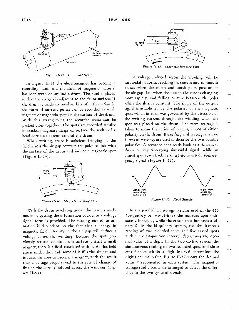
II-46 IBM 650
Figure II-53. Drum and Head
In Figure II-53 the electromagnet has become a recording head, and the sheet of magnetic material has been wrapped around a drum. The head is placed so that the air gap is adjacent to the drum surface. If the drum is made to revolve, bits of information in the form of current pulses can be recorded as small magnets or magnetic spots on the surface of the drum. With this arrangement the recorded spots can be packed close together. The spots are recorded serially in tracks, imaginary strips of surface the width of a head core that extend around the drum.
When writing, there is sufficient fringing of the field across the air gap between the poles to link with the surface of the drum and induce a magnetic spot
(Figure II-54).
Write Circuits
o
o
Figure II-54. Magnetic Writing Flux
With the drum revolving under the head, a ready means of getting the information back into a voltage signal form is provided. The reading out of information is dependent on the fact that a change in magnetic field intensity in the air gap will induce a voltage across the winding. Because the spot previously written on the drum surface is itself a small magnet, there is a field associated with it. As this field passes under the head, some of it fills the air gap and induces the core to become a magnet, with the result that a voltage proportional to the rate of change of flux in the core is induced across the winding (Fig
ure II-55).
-<To Read Circuits
Figure II-55. Magnetic Reading Flux
The voltage induced across the winding will be sinusoidal in form, reaching maximum and minimum values when the north and south poles pass under the air gap; i.e., when the flux in the core is changing most rapidly, and falling to zero between the poles when the flux is constant. The shape of the output signal is established by the polarity of the magnetic spot, which in turn was governed by the direction of the writing current through the winding when the spot was placed on the drum. The term writing is taken to mean the action of placing a spot of either polarity on the drum. Recording and erasing, the two forms of writing, are used to describe the two possible polarities. A recorded spot reads back as a down-updown or negative-going sinusoidal signal, while an erased spot reads back as an up-dawn-up or positil,egoing signal (Figure II-56).
S.gnal from recorded spot (Binary "I")
Figure II-56. Read Signals
Signal from erased spot (Binary "0")
In the parallel bit storage systems used in the 650 (bi-quinary or two-of-five) the recorded spot indicates a binary 1, while the erased spot indicates a binary O. In the bi-quinary system, the simultaneous reading of two recorded spots and five erased spots within a digit-position interval determines the decimal value of a digit. In the two-of-five system the simultaneous reading of two recorded spots and three erased spots within a digit interval determines the digit's decimal value. Figure II-57 shows the decimal value 7 represented in each system. The magneticstorage read circuits are arranged to detect the difference in the two types of signals.
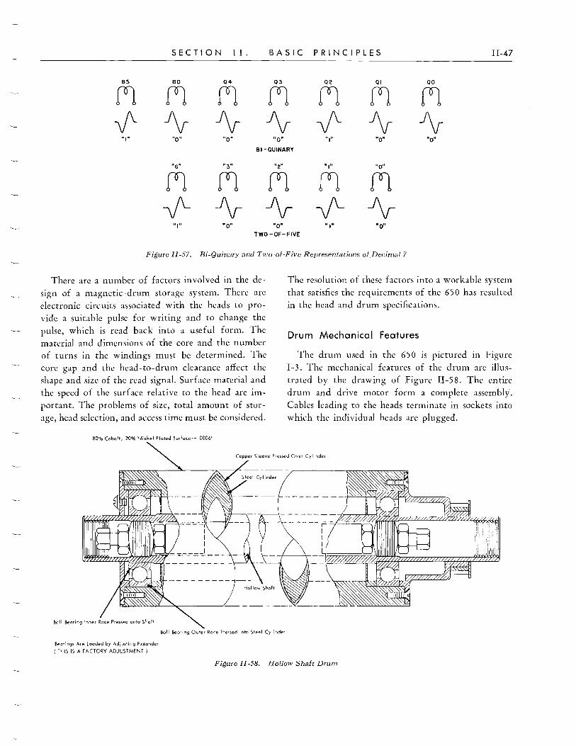
SECT10N I I . BAS I C PRINCIPLES II-47
B5 BO 04 03 02 01 00
r1 r1 r1 r1 r1 [0) r1 J'- -Av -Av -Av -J'- -Av -Av
"." "0" "0" 110 11 "I" "0" "0"
BI-QUINARY
"6" "3" ··2" 11111 ··0"
r1 r1 r1 r1 r1 -JL -iV- -iV- -JL -iV-
"111 ·0· ·0· "." 11 0"
TWO-OF-FIVE
Figure II-57. Bi-Quinary and Two-oi-Five Representations of Decimal 7
There are a number of factors involved in the design of a magnetic-drum storage system. There are electronic circuits associated with the heads to provide a suitable pulse for writing and to change the
pulse, which is read back into a useful form. The material and dimensions of the core and the number of turns in the windings must be determined. The core gap and the head-to-drum clearance affect the shape and size of the read signal. Surface material and the speed of the surface relative to the head are important. The problems of size, total amount of stor
age, head selection, and access time must be considered.
80% Cobalt, 20% Nickel Plated Surfoce-- 0006"
Bearings Are Loaded b>' Adjusting Expander
( THIS IS A FACTORY ADJUSTMENT)
Ball Bearing Outer Race Pressed into Steel Cylinder
The resolution of these factors into a workable system that satisfies the requirements of the 650 has resulted in the head and drum specifications.
Drum Mechanical Features
The drum used in the 650 is pictured in Figure 1-3. The mechanical features of the drum are illustrated by the drawing of Figure II - 58. The entire drum and drive motor form a complete assembly. Cables leading to the heads terminate in sockets into
which the individual heads are plugged.
Figure II-58. Hollow Shaft Drum
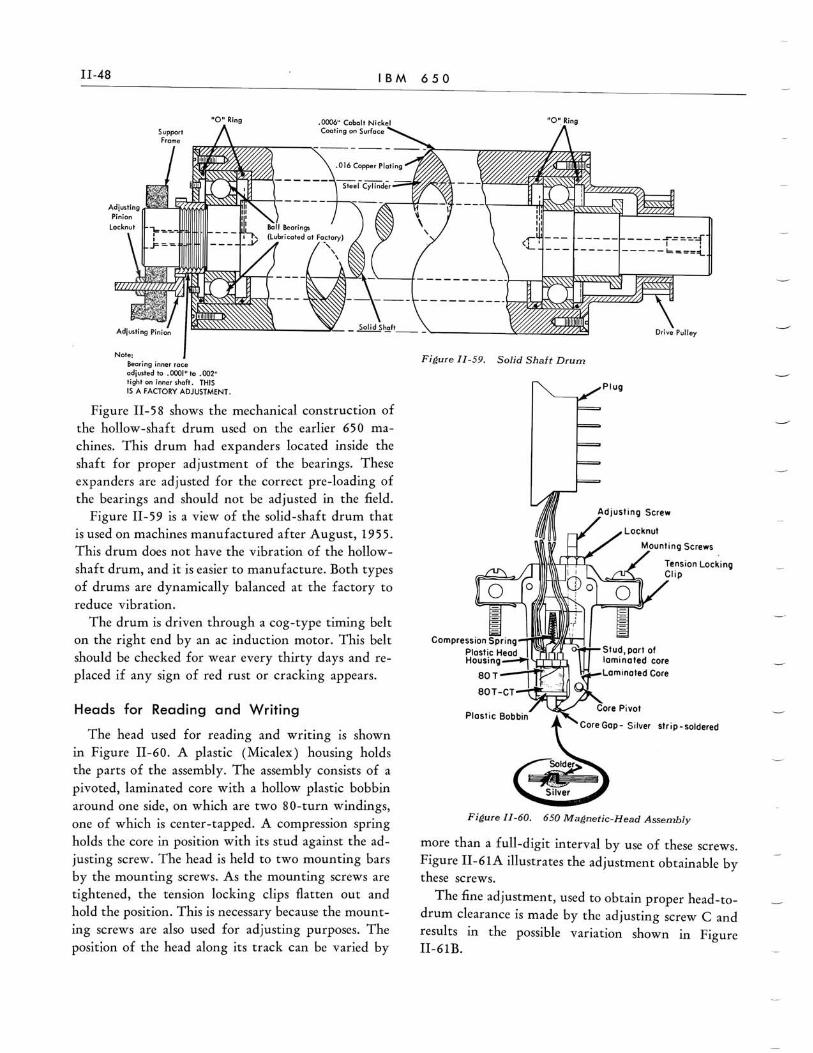
II-48 IBM 650
Note: Bearing inner race adjusted to .0001" to .002" tight on inner shoft. THIS IS A FACTORY ADJUSTMENT .
Figure II-5S shows the mechanical construction of the hollow-shaft drum used on the earlier 650 machines. This drum had expanders located inside the shaft for proper adjustment of the bearings. These expanders are adjusted for the correct pre-loading of the bearings and should not be adjusted in the field.
Figure II-59 is a view of the solid-shaft drum that is used on machines manufactured after August, 1955. This drum does not have the vibration of the hollowshaft drum, and it is easier to manufacture. Both types of drums are dynamically balanced at the factory to reduce vibration.
The drum is driven through a cog-type timing belt on the right end by an ac induction motor. This belt should be checked for wear every thirty days and replaced if any sign of red rust or cracking appears.
Heads for Reading and Writing
The head used for reading and writing IS shown in Figure II-60. A plastic (Micalex) housing holds the parts of the assembly. The assembly consists of a pivoted, laminated core with a hollow plastic bobbin around one side, on which are two SO-turn windings, one of which is center-tapped. A compression spring holds the core in position with its stud against the adjusting screw. The head is held to two mounting bars by the mounting screws. As the mounting screws are tightened, the tension locking clips flatten out and hold the position. This is necessary because the mounting screws are also used for adjusting purposes. The position of the head along its track can be varied by
Figure II-59. Solid Shaft Drum
Compression Spring-T1~~fi:-1 Plastic Head Housing~
80 T __ ~~;::"J
80T -CT.....; ..... ~~I
Plug
Tension Locking Clip
str ip - soldered
Figure Il-60. 650 Magnetic-Head Assembly
more than a full-digit interval by use of these screws. Figure II-61A illustrates the adjustment obtainable by these screws.
The fine adjustment, used to obtain proper head-todrum clearance is made by the adjusting screw C and results in the possible variation shown in Figure II-61B.
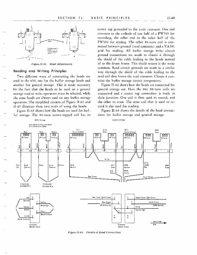
o o
Mount"'9 Bors
Turtllno strew A 9'vK __ _
Turnlo9 serew B 9'ves. _____ _
SECTI"ON II.
o o
Figure lJ-61. Head Adjustments
Reading and Writing Principles
Two different ways of connecting the heads are used in the 650, one for the buffer storage heads and another for general storage. This is made necessary by the fact that the heads to be used on a general storage read or write operation must be selected, while the same heads are always used on any buffer storage operation. The simplified circuits of Figure II-62 and II-63 illustrate these two ways of using the heads.
Figure II-63 shows how the heads are used for buffer storage. The SO-turn center-tapped coil has its
80 Turns
Bvffer Storoge
Sync Heoch Similar with Read Coil Connections Only
c . .5
Ero~e Record
c _____ ~
Read Read Erose Write Sig <;:ommon Common
Qlth
80 Turns
,------------,I 2 1- _________ _
Record Qllh Record
BASIC PRINCIPLES II-49
center tap grounded to the write CO III 1JlOn. One end connects to the cathode of one half of a PW503 for recording, the other end to the other half of the PW503 for erasing. The other SO-turn coil is connected between ground (read common) and a VA501 grid for reading. All buffer storage write circuit ground connections are made to chassis 6 through the shield of the cable leading to the heads instead of to the drum frame. This shield return is the write common. Read circuit grounds are made in a similar way through the shield of the cable leading to the read coil that forms the read common. Chassis 6 contains the buffer storage circuit components.
Figure II-62 shows how the heads are connected for general storage use. Here the two SO-turn coils are connected and a center tap connection is made at their junction. One coil is then used to record, and the other to erase. The same coil that is used to record is also used for reading.
Figure II-64 shows the details of the head connec
tions for buffer storage and general storage.
Qlth Ero~e
General Storoge
OOth
Olth ErO$e
Red Tracer
QOlh
OOth Erose
Blue Tracer
1 Conductor 2 Conductor Shielded Wire Shielded Wire
.-----_ .. , Red: 5 :
t (Record) I I : ~ i Yellow "-
Yellow: 3 I (Read 5ig) "
--(::-Ec-os~e)"':-O : I 2: Shield / I 0 I ' I I (Read Common)
Shield I 4 I t
(Write Common) : t t '-------,
Connector (ScHorn View)
~-----1 r-----' Red Tracer (Qlth Ero~e): 5 I I: 05 ,: Green Tracer (OOth Erose)
--------------~----~I-O I ~ . I I I I
Figure II-64.
Blue Tracer I b:! 6 ... .;.:I'--------~B:.;.I.:..:C.;.k ;..Tc.:...c.:..ec ____ _
(Q1th Record) : : (QOth Record) I 3 -+'~:~~~ __ ~:.:..w.;.hi.:..'e~ ________ ___ i ~ i! b! (Cenlec Top)
: 4 : 4 : 010 I
t I I I I L _____ : L _____ J
Connector (Bottom Vie.,...)
Details of Head Connections
Sync Track.
End

fR(lM ADDRESS REGISTER
Q 8
" 7
RIGS
B 5 TO G,S GATE
ws,o---------------~
OITH 0----------------<1
"OU 81T o-----Q:INF"O GATES
-t2,5l:1 I I
""O~
-50~
'90 1 '.IOO~
I
VO I H QI1H
BCD tJ. e c I I I
'l"0 ~-50
nJo "0
10
I1_ ). t:: i.1'<:::-7" _-_-_64V--<>-_--I-_
WD 4-10
Figure JI-62. General Storage Head Connection and Read-Write Circuitry
11-50

l~ -0
o .: .. o r a-A '"'0 GA'E
wSP
WRoTE 1 WROTE CURRENT
l FLUX
A OUTPUT FOR iRASEO SPOT
RS'
NLRP
RS'
C 0 A B
~ I
A I
II-51
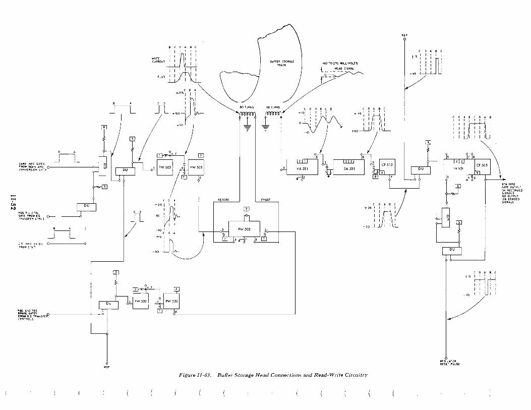
...... ...... &. ~
UAp INFO GATES ".OM SCAN AND tONV(RSIO"'l CKTS
~&S ,. ~ CnlL. ~( MloM 8S r~ANSr£R tTAL.S
~! fNFO GATES ".OM ~1C7
fi'1S ANO PBS 1~A5( GATeS -(110M B 50 'P'RAoNSF[ CO",!"IQOlS
J---i
• • ~~
wsp
WRIT' CURRENT
Jt
CD'
"t251~:: I I -'0
I I
-.40 C DUI T.D: hL
-50 --L
Figure I I -63.
BUFFER STORAGE TRACK
eo TURfolS
160 TO 270 MILLIVOLTS
l HEAD SIGNAL.
;~ C-
CDABCD :'V( + 145
+So
t 1"35 I
-50
Buffer Storage Head Connections and Read-Write Circuitry
osp
: 1: i) 1 1 •
I!...-
• t I i
tIS
;/
NEG LATe'" RESET pUL,SE
B~A INFO GATE OuTPuT ON RECORDED SIGNALS NO OuTPUT ON [RASIO SIGNALS

SEC T.I 0 N I I .
The general storage circuits represented in Figure II-62 will be used to explain the principles of magnetic writing and reading.
When placing information in general storage, the object is to place the spot on the drum in such a position that when it is later read out it will cause the read circuits to produce an on time B-A information gate; i.e., if the spot is to represent Dl, it should when read out, cause a B-A information gate to be developed during the Dl timing interval. It should be remembered that all information is transmitted throughout the machine in the form of B-A gates. Reference to Figure 1-11 will show that information can be sent to general storage from either the distributor or from read buffer storage. Thus, the output from these units must be in the form of B-A information gates, which, when allowed to reach the general storage input, will actuate the write circuits.
Because time is required to write and to read, the general storage write circuits must be actuated in advance of the drum time of the digit to be stored, if the digit is later to be available from the general storage read circuits as on time B-A gates. In this machine, the magnetic storage circuits have been designed so that one whole digit time is used in the process of writing and reading. Thus, the B-A gates from either distributor or read buffer storage, which actuate the general storage write circuits, must be one-digit time early with respect to the drum time of the digit that they represent. The spots will then be placed on the drum in such a position as to cause the read circuits to put out on time B-A gates when they are read out. In other words, general storage receives information in the form of one digit early B-A gates and puts out information as on-time B-A gates.
It will be remembered that the distributor, a capacitor storage unit, has both a one-digit-early output and an on-time output. The one-digit-early output is used when information is sent from the distributor to general storage. It will be seen also that information is written in read buffer storage at such a time that it will be available from the buffer storage read circuits one digit early for proper entry into general storage.
Figure II-62 shows a part of the circuitry of the general storage read-write matrix. The outputs from the address register will have activated the selection
BASIC PRINCIPLES II-53
circuits so that the potential of the center tap will have been rasied from - 70 volts to + 100 volts due to conduction of the PW505 as shown, thus readying the selected head for use. A one-digit-early, B-A gate present on one of the bit input terminals will activate the record circuit. (Only the 0 bit circuits are shown.) If the value of the digit is such that no information gate is present, this lack-of-information signal level is inverted, and the erase circuit will be activated instead of the record circuit.
At C time of the digit interval a write sample pulse will be present on either the Ql TH or the QOTH line, depending on the output of the address register (assume QOTH). This WSP will switch with the B-A gate to operate the record circuit or with the no B-A gate inverted to operate the erase circuit. With the trailing edge of the WSP a sharp, short voltage pulse is produced as shown by the wave forms associated with the PW502. This pulse causes the PW507 to conduct heavily for the short time of the pulse, thus energizing either the record or erase coil to place a spot on the drum. The complete circuit to energize the head is:
Ground, cathode of PW507, anode, DD501, coil, cathode of PW505, anode, 250-volt write circuit supply.
The PW507 is caused to conduct for about 1 Yz microseconds by the pulse on its grid. Write current flows through the coil during this time as shown by the wave form associated with the coil.
A timing chart showing the relation of the important factors involved in writing and reading is shown on the right end of Figure II-62. Notice that a pattern of the flux distribution on the drum surface due to the write current is shown and that the flux is slightly offset from the current. This time phase shift is due to the rapid movement of the drum surface during the current time interval. The diagram in the Note shows what the current-flux-time relationship would be if the drum were not moving.
The flux also appears to be spread over a greater time interval than the current. This is because the leakage flux around the core air gap of the head cannot be concentrated in a single point but affects an area of the surface either side of the point directly under the gap. Because of the drum motion and this
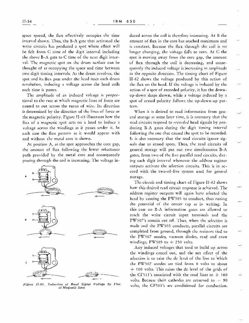
II-54 IBM 650
space spread, the flux effectively occupies the time interval shown. Thus, the B-A gate that activated the write circuits has produced a spot whose effect will be felt from C time of the digit interval including the above B-A gate to C time of the next digit interval. The magnetic spot on the drum surface can be thought of as occupying the space and time between two digit timing intervals. As the drum revolves, the spot and its flux pass under the head once each drum revolution, inducing a voltage across the head coils each time it passes.
The amplitude of an induced voltage is proportional to the rate at which magnetic lines of force are caused to cut across the turns of wire. Its direction is determined by the direction of the lines of force or the magnetic polarity. Figure II-65 illustrates how the flux of a magnetic spot acts on a head to induce a voltage across the windings as it passes under it. In each case the flux pattern as it would appear with and without the metal core is shown.
At position A, as the spot approaches the core gap, the amount of flux following the lower reluctance path provided by the metal core and consequently passing through the coil is increasing. The voltage in-
B
4--
Figure JI-65. Induction of Read Signal Voltage by Flux of Magnetic Spot
duced across the coil is therefore increasing. At B the amount of flux in the core has reached maximum and is COllstant. Because the flux through the coil is no longer changing, the voltage falls to zero. At C the
spot is moving away from the core gap, the amount of flux through the coil is decreasing, and consequently the induced voltage is increasing in amplitude in the opposite direction. The timing chart of Figure II-62 shows the voltage produced by this action of the flux on the head. If the voltage is induced by the action of a spot of recorded polarity, it has the downup-down shape shown, while a voltage induced by a
spot of erased polarity follows the up-down-up pattern.
When it is desired to read information from general storage at some later time, it is necessary that the read circuits respond to recorded head signals by producing B-A gates during the digit timing interval following the one that caused the spot to be recorded. It is also necessary that the read circuits ignore signals due to erased spots. Thus, the read circuits of
general storage will put out two simultaneous B-A gates, from two of the five parallel read circuits, during each digit interval whenever the address register outputs activate the selection circuits. This is in accord with the two-of-five system used for general storage.
The circuit and timing chart of Figure II-62 shows how this desired read circuit response is achieved. The address register outputs will again have selected the head by causing the PW505 to conduct, thus raising the potential of the center tap as in writing. In this case no B-A information gates are allowed to
reach the write circuit input terminals and the PW507's remain cut off. Thus, when the selection is made and the PW505 conducts, parallel circuits are completed from ground, through the resistors tied to the PW507 anodes, vacuum diodes, read and erase windings, PW505 to + 250 volts.
Any induced voltages that tend to build up across the windings cancel out, and the net effect of the selection is to raise the dc level of the hne to 'which the PW507 anodes are tied from 0 volts to about + 100 volts. This raises the dc level of the grids of t,he CF511's associated with the read lines to + 100 volts. Because their cathodes are returned to + 90 volts, the CF511's are conditioned for conduction.

SECTION II.
One of the pair of CF511 triodes, whose anodes are normally blocked by action of the PW504's used as blocking inverters, will be unblocked by QTH selection from the address register. This one will conduct and drive the VA502. After the selection transient has died out, the induced ac head signal present across the read winding and superimposed on the 100-volt selection level, continues to drive the unblocked CF511 and thus becomes the input signal to the VA502. The output of the VA502 is then an amplified replica of this ac head signal.
The dc component of the VA502 output is removed by the input capacitor of the SA501, and the signal on its grid is shown by the accompanying wave form. The output of the SA501, which responds only to positive changes in the input signal, is shown by the wave form diagram and in the timing chart. The timing chart shows how the shaping amplifier responds differently to recorded and erased signals. N 0-
tice that a shaping amplifier output from a recorded
signal overlaps the time of the read sample pulse (RSP), while that of an erased signal does not coincide. Thus, there is an RSP output from the diode switch on recorded signals and no output on erased signals. This pulse turns the output latch on at B time. The latch is reset every A time by a negative
latch reset pulse. The output of the latch is the necessary on-time B-A information gate. These B-A gates pass through the 5-to-7 conversion circuits, where they are converted to the 2-of-7 bi-quinary system of digit-value representation for transmission to distributor, program register, or adder.
This action takes place continuously as long as a valid general storage address is in the address register. Information gates from a whole selected band of general storage are therefore available from the output latches. The desired series of B-A gates is selected from this train of information by the read-in
switching circuitry of the unit that is to receive the information as directed by the program control cir
cuits. Reference to wiring diagram section 4-10 depicting
the general storage read-write circuits will show that a combination of circuitry, like that of Figure II-62, accomplishes all writing into and reading from general storage.
Figure II-63 is typical of the buffer storage CIrcuitry used to record, erase, and read. The main dif-
BASIC PRINCIPLES II-55
ference here is in the way the heads are connected. No head selection is necessary, less circuitry is needed, and the head circuits are completed to ground. Because there are fewer components in series with the head windings, less voltage is needed, and the PW502's and 503's have their anodes returned to + 150 volts instead of + 250 volts as in general storage circuits.
Information gates from the seven parallel buffer storage read circuits are continuously available from the output latches. (Only one circuit is shown.) On a read operation, a 10-word control gate coinciding in time with RBS, allows these B-A information gates to get through switches to operate the general storage write circuits, thus transferring the 10 RBS words to the selected general storage band. As soon as this transfer is complete, a similarly timed control gate (RBS erase gate) is applied to the diode switch as shown, gating through a WSP for each digit of each of the RBS words to operate the erase circuits and erase RBS to blanks. The card information gates from
the cathode follower scanning matrix are then gated through to operate the record windings of RBS, by repeated usage of an RBS read-in control gate on several drum revolutions, and transfer the card information to RBS. This information will be similarly transferred to a selected general storage band on the next read operation. The foregoing control gates are developed by the buffer storage transfer and erase controls. These controls are activated by input or output operation codes.
On a punch operation a PBS erase gate that coincides in time with PBS is applied to the diode switch, gating through a WSP for each digit of each PBS word, to operate the erase circuits and erase PBS to blanks. As soon as this erasure is completed, on the next drum revolution, a similarly timed control gate
\ (PBS read-in) is applied to diode switching as shown to allow the 5-to-7 converted B-A output gates of this portion of a selected general storage band to operate the buffer storage record circuits, thus transferring the information to be punched to PBS. The information now in PBS is then scanned out to punch by repeated usage of a PBS read-out gate on several successive drum revolutions.
The wave forms at key points of the circuits are shown and are similar to those of the general storage circuits.

II-56 IBM 650
1'2
+3-,...,--, /
I /
" -100 ~
~ __ ~-~-~--6
From Heads
D A +250U +195, 1
I I +160 1 ___ 1
-30
To Storage Check
Latch
/l +25
L..l..-50
-70 CF 504
Figure II -66. Multiple Write Circuit
MULTIPLE-WRITE-NO-WRITE CIRCUIT
THE 650 is designed as a self-checking machine.
There are circuits built into the machine for checking
information as it is transferred about the machine. In order to carry the self-checking throughout the
machine, there are check circuits on the magnetic
drum write circuits.
This checking is done by the circuit located on wir
ing diagram 4-10 ED. In this circuit the amount of
current flowing through the heads develops a voltage across five resistors, and this voltage in turn is checked
by the 1nultiple-write-no-write circuit. These five resistors may be found on wiring diagrams 4-10 and
4-13.
Multiple Write
The multiple-write circuit (Figure 11-66) is a schematic drawing of the circuit on wiring diagram 4-10ED. The purpose of the multiple-write circuit is
to detect whether more than one band of heads is writing simultaneously. The sensitivity of the circuit
is capable of indicating an error if seven or more
heads are conducting simultaneously. The circuit sam
ples the voltage developed across the five resistors.
The normal voltage swing is about +250 to +195 volts. This is not enough change to produce an out
put pulse. A greater negative swing will produce a
positive output pulse, which is used to turn on the storage check latch.
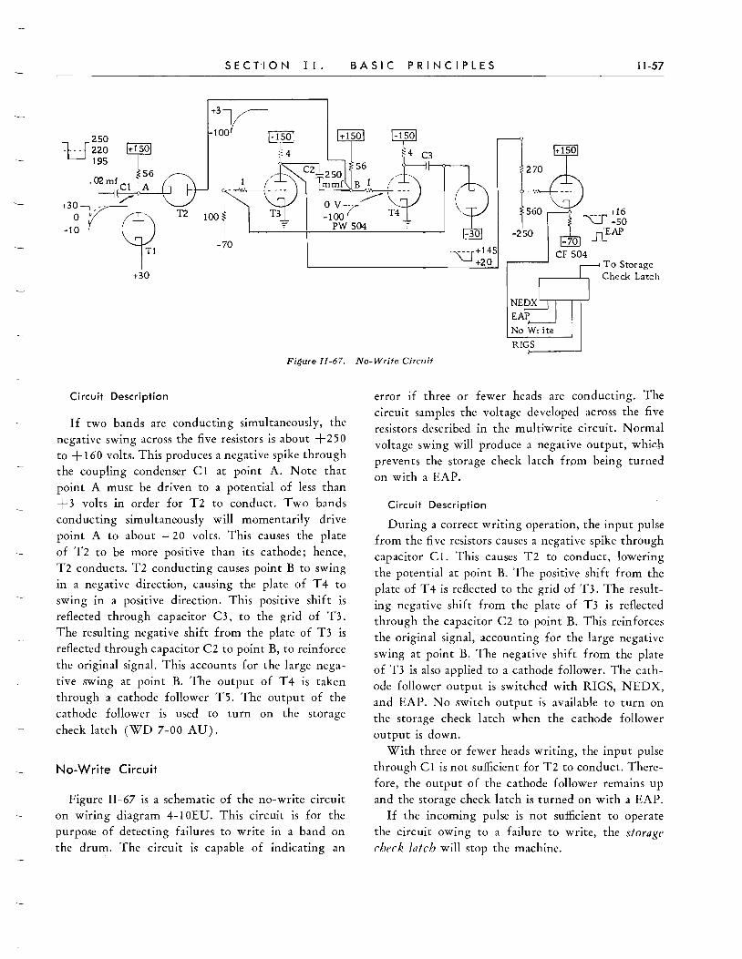
250 U 220 +150 195
56 .02mf C1 A
-l/ +30l,~
o V ( -10
+30
SEC TI ON I!.
T2
-70
BASIC PRINCIPLES II-57 ----------------------------
'CJ+145 +20
No Write
RIGS 1-----'
To Storage Check Latch
Figure II -67. No-Write Circuit
Circuit Description
If two bands are conducting simultaneously, the negative swing across the five resistors is about +250 to + 160 volts. This produces a negative spike through the coupling condenser C1 at point A. Note that point A must be driven to a potential of less than + 3 volts in order for T2 to conduct. Two bands conducting simultaneously will momentarily drive point A to about - 20 volts. This causes the plate of T2 to be more positive than its cathode; hence, T2 conducts. T2 conducting causes point B to swing in a negative direction, causing the plate of T 4 to swing in a positive direction. This positive shift is reflected through capacitor C3, to the grid of T3. The resulting negative shift from the plate of T3 is reflected through capacitor C2 to point B, to reinforce the original signal. This accounts for the large negative swing at point B. The output of T 4 is taken through a cathode follower T5. The output of the cathode follower is used to turn on the storage
check latch (WD 7-00 AU).
No-Write Circuit
Figure II-67 is a schematic of the no-write circuit on wiring diagram 4-10EU. This circuit is for the purpose of detecting failures to write in a band on the drum. The circuit is capable of indicating an
error if three or fewer heads are conducting. The circuit samples the voltage developed across the five
resistors described in the multiwrite circuit. Normal voltage swing will produce a negative output, which prevents the storage check latch from being turned on with a EAP.
Circuit Description
During a correct writing operation, the input pulse from the five resistors causes a negative spike through capacitor C1. This causes T2 to conduct, lowering the potential at point B. The positive shift from the plate of T 4 is reflected to the grid of T3. The resulting negative shift from the plate of T3 is reflected through the capacitor C2 to point B. This reinforces the original signal, accounting for the large negative
swing at point B. The negative shift from the plate of T3 is also applied to a cathode follower. The cathode follower output is switched with RIGS, NEDX, and EAP. No switch output is available to turn on the storage check latch when the cathode follower output is down.
With three or fewer heads writing, the input pulse through C1 is not sufficient for T2 to conduct. Therefore, the output of the cathode follower remains up and the storage check latch is turned on with a EAP.
If the incoming pulse is not sufficient to operate the circuit owing to a failure to write, the storage check latch will stop the machine.

II-58 IBM 650
SEVEN-TO-FIVE AND FIVE-TO-SEVEN
TRANSLATOR CIRCU ITS
INFORMA TION from the distributor (on a store operation) or from read buffer storage (on a read opera
tion) , must be changed from its 2-of-7 bi-quinary form to the 2-of-5 system used by general storage.
Also, 2-of-5 information from the general storage read-out latches must be changed back to the 2-of-7 bi-quinary form before it is sent to the selected stor
age line or to punch-buffer storage.
These conversions are done by the 7 -to-5 and
5 -to-7 - translator circuits. The position of these cir
cuits in the data flow paths is shown in WD 0-99. The circuit details are shown in section 4-00 of the
wiring diagram.
The chart at the top of section 4-00 shows which pair of bits must be present, in each system, to repre
sent each possible decimal digit value.
Seven-te-Five Circuits
Bi-quinary output lines from the distributor and from buffer storage enter the 7-to-5 circuits in 4-00
AU. Information on either of these inputs is gated through to the 7 -to-5 matrix by the presence of either a RIGS gate (developed by program control on 20 codes) or a BS to GS gate (developed by program control on a 70 code).
The chart shows that information gates on the BO
and QO input lines must cause similar gates to be present on the 1 and 2 output lines. BO and Q 1 gates must cause a and 1 outputs, etc.
Further analysis of the chart will show that several input combinations must produce gates on each of the output lines. These combinations are outlined in the
following table. The 7 -to- 5 switch and mix circuits serve to accomplish these objectives.
Outputl Line I
o 1 2 3 6
Input Conditions ~-=----:--c=--
Any Qt, EO and Q2, BO and Q3 BO and QO, EO and Ql, BO and Q4, B5 and Q2 Any QO, BO and Q2, B5 and Q3 Any Q4, BO and Q3, B5 and QO E5 and Qt, or Q2 or Q3 or Q4
Five-te-Seven Circuits
The 2-of-5 output lines from the general storage read-out latches bring information to the 5-of-7 circuits. The following table shows which input com
binations must produce a gate on each output line.
Output I _ Line __ I_Input Conditions
QO -2andlor3 Q1 J 0 and t or 6 Q2 I 2 and 0 or 6 and 1 Q3 3 and 0 or 6 and 2 Q4 I 3 and 1 or 6 Bo : 1 and 2 or 1 and 0 or 2 and 0 or 3 and 0 or 3 and 1 B5 I Any 6 or 3 and 2
The 5-to-7 switches (WD 4-00 CU) are further conditioned by a negative latch reset pulse and storage control (WD 4-00 BU). The negative latch reset pulse helps to cut off the trailing edge of the 5-to-7 output gates sharply at A time. The storage control insures that there will be no general storage latch output on the selected storage line on a manual read-in to general storage operation.
SELECTED STORAGE SWITCHING
REFERENCE to WD 0-99 shows the purpose of selected storage switching. The selected storage, bi
quinary, data flow lines that take information to distributor, program register, and adder can be supplied from any general storage band, upper or lower accumulator, distributor, or storage entry switches. T t is the function of selected storage switching to gate information through to the selected storage lines from accumulator, distributor, or storage entry switches in accordance with the particular 800X address.
The details of these circuits are shown in section 5-00 of the wiring diagram.
Figure 11-68 is a simplified circuit of the Q4 bit
line of selected storage switching. This is a composite view of the circuits that are located on wiring diagrams 5-00, 5-10, 6-10, 6-20, and 8-00.

SEC T·I 0 N I I . BASIC PRINCIPLES II-59
~,:o_J-- --- - -- -- - -- - - - - - - ~=I='-:'= i- - -T~_~O'----L6:.'2' 18::0.9.J TO I TO TO 1
ACC+ ACC-
015T ON-TIME
OUTPUT
Ace ON TIME LATCHES
7E
NAP
ADOR 8001
Ace ON HME OUTPuT
AD ER I PR GREG. DIST.
I
RIPS
4X, ,200 ;
SEL STOR. : I I ADO GATE I I
I " I
R' 0151.
~ _____ -' , _________ .J __ _______ J
I
I I ,.---1------- - -----r--
~5.:~ _I
I ,
128
I I I I I.
I STDR I I ENTRY I I SWITCHES I
----1 ________ ......
Figure 1I-68. Selective Storage Switching
VALIDITY CHECK CIRCUITS
Capacitor Storage Validity Check Circuits
The 650 is designed as a self-checking machine. There are circuits in the machine to keep a continuous
check on the contents of the three capacitor storage units within the machine. These units are the accumu
lator, the program register, and the distributor.
The check circuits are designed to check the bi
quinary number system for valid information. It has been proved that practically every circuit failure will
affect the valid 2-of-7 code system. It is only necessary then to design a circuit that
will check for the presence of one and only one binary bit and one and only one quinary bit at each digit time. In this manner the machine can detect extra bits or missing bits in the capacitor storage units.
Because every piece of information that enters the machine must flow through at least one of these units
at some time during the course of a problem, this sys
tem will detect errors in any data of instructions handled by the machine.
In order to check for extra bits, it is necessary to check for the following bit combinations:
BO & B5
QO & QI
QO & Q2
QO & Q3
QO & Q4
QI & Q2 QI & Q3 QI & Q4 Q2 & Q3 Q2 & Q4 Q3 & Q4
A schematic of a circuit to check this is shown in
Figure II-69. Any combination of the above will cause an error indication.

II-60 IBM 650
85 04 04 03 03 02
02
03
04
01
00
01 00
80
85
J""1..Error r-----'T"""~lndjcotion
Figure 11-69. Validity Check Schematic
This circuit will also check for missing bits by inverting the no-signal output from a diode switch and using that as the error indication.
Wiring diagram 6-30 shows the validity-check circuits in detail. There are three separate circuits, one for each capacitor storage unit. The output of each will turn on an error latch, which in turn will stop the machine and turn on the proper error light.
Buffer Storage Validity Check Circuits
Buffer storage validity check circuits are being incorporated in 650 machines beginning with about 650-10489 to increase the checking features of the
machine. The checking feature is controllable from the con
trol panel of the input-output device. The inputoutput device will control the checking feature for only the buffer it is using. This control is selectable between cards and consists of automatic checking circuits unless it is controlled off. The OFF position must be wired to make the checking device inoperative.
Checking is suspended for all load cards.
All ten words of input and output are checked. Therefore, if the checking feature is used, all words of input and all words of output must contain valid information.
If a failure occurs on the input from the reader, it will be detected when the information is being transferred to general storage. The storage check latch and the address selection light will be turned on. The RBS timer will be held OFF to prevent the erase of
buffer storage. The reader will feed the next card, but the information from this card will not be allowed to enter buffer storage. Therefore, the reader must be cleared, and the run restarted with the error card.
If an error occurs during output scanning, a validity check latch for that particular buffer will be turned on. This latch output will set the storage check latch, turn on the storage selection light, and stop the machine the next time the output code controlling this same buffer area is used. Therefore, even though an error on the output is detected, the machine will not necessarily stop immediately.

Example Program: Read Code 70 Arith. Code --Store Code ---
SECTION II.
Punch Code 71 --- Error In Punching
Store Code Punch Code 74 Read Code 70 Arith. Code ---Store Code ---Punch Code 71 --- Machine Stops (N 0 erase, transfer, or punching takes place)
Objectives:
READ VALIDITY CHECK
The objectives of the read validity check circuits ~lre to check the validity of the information being transferred to general storage, and if an error occurs, stop the machine, turn on the storage check latch, turn on the storage selection light, and prevent erase of the information containing the error.
Circuits:
READ VALIDITY CHECK (WD 6-33) The output of buffer storage output latches switches
and mixes to determine whether there is at least one binary and one quinary. The output is also switched and mixed to determine whether there is more than one binary or more than one quinary. If there is not at least one binary and one quinary or if there is more than one binary or more than one quinary, a cathode follower output will switch with ND10, DP and RVe Timer I and II to turn on the read validity check latch. This latch will be turned off with error
reset. The R ve Timer I 1171d II is a result of switching the
BS to GS Trf. gate buffer I and II with buffer I RBS transfer latch output to drive a cathode follower. The plate supply of this CF is a result of control panel wiring of the machine tied to buffer I (R VC not
plugged) . R ve Timer I and II may also be a result of switch
ing the BS to GS Trl. gate buffer I and II with buffer II RBS transfer latch output to drive a cathode follower. The plate supply of the CF is a result of control panel wiring of the machine tied to buffer II
(RVC not plugged).
BASIC PRINCIPLES 11-61
Buffer III is checked in a similar manner. The output of Buffer III is switched and mixed to determine whether there is at least one binary and one quinary, but no more than one of each. If there is an error, the output of a CF will switch with RVe Timer Ill, ND 1 0, and DP to turn on the read validity check latch.
The RVe Timer III is the result of switching the BS to GS Trf. gate buff('r III with Buffer III RBS transfer latch output to drive a cathode follower. The plate supply of this CF is the result of control panel wiring of the machine tied to buffer III (R VC not plugged) .
The output of read validity check latch will immediately set the storage check latch and prevent any further restarts. The output will also switch with Neg. R ve Timer I, II and III to hold off the RBS Timer for buffer I or II and prevent the completion of the read code operation. Only the transfer (of the transfer, erase and scall operation) will take place. The invalid information will be held in the buffer
area.
Objectives:
OUTPUT VALIDITY CHECK
The objectives of the output validity check circuits are to check the validity of information being punched; and if an error is detected, prevent erase of the invalid information, stop the machine, and turn on the storage check latch and storage selection light.
Circuits:
OUTPUT VALIDITY CHECK (WD 6-33) The same switching circuit used to check the input
validity is used to check output validity. An output validity check latch is turned on by switching the output of the check circuit with NDO, DP and PVC Timer (WD 6-33).
The PVC Timer is a gate developed for each punch (print) digit time by switching PBS Timer at a CF with the plate voltage determined by the control panel wiring and a timing cam (P44 on the 533) on the output device.
Because it is desirable to check validity during punching (printing), and use the operation register to indicate the error buffer, three output validity check latches are used. \Vhen an output validity error occurs, the output device is in its output cycle.
II-62 IBM 650
The error turns on the corresponding output validity check latch. The control commutator restart will have previously taken place. Therefore, the control commutator cannot be held up at this time. The validity check latch prevents the associated output code latch from turning on, and turns on the storage check latch, when the operation register calls for the next output code associated with the error buffer.
The output validity check latch is reset from the error reset line.
533 Read Validity Check Circuits
The R VC circuits in the 533 are controlled by R214 (28A). The R214-2N/C (27 A) point will provide plate voltage to the CF507 at 4M (3-30B). Plate voltage at this CF will allow the RVe Timer gate to be developed. Rve Timer gate is necessary to turn on the read buffer check latch if an error occurs.
To make the checking operation inoperative, R214 must be picked. This may be accomplished by wiring R VC OFF; or by R260-12N/o point on load cards.
------
Digit impulses through R26 and 27 will pick R214. The hold circuit is through R8 until 3520.
Validity will not be checked on run-in. Read codes are necessary for the checking operation and do not occur on run-in.
533 Punch Validity Check Circuits
The punch validity check circuits on the 533 are controlled by R215 (3B). The R215-2N/C (6A) point will provide plate voltage to the CF 507 at 3P (3 -3 OC) . Plate voltage at this CF will allow the PVC Timer to be developed. PVC Timer is necessary to turn on the output validity check latch.
To make the checking operation inoperative, R21 5
must be picked. This may be accomplished by wiring PVC-OFF. If PVC-OFF is wired, R215 will be picked and held from 13.8 to 9.3.
The hubs are located as follows on the 533 Control
panel: RVC PVC
OFF OFF
AR 43 and 44 AR 45 and 46
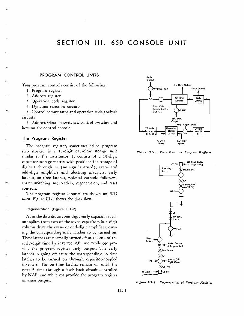
SECTION III. 650 CONSOLE UNIT
PROGRAM CONTROL UNITS
THE program controls consist of the following: 1. Program register 2. Address register 3. Operation code register 4. Dynamic selection circuits 5. Control commutator and operation code analysis
circuits 6. Address selection switches, control switches and
keys on the control console
The Program Register
The program register, sometimes called program step storage, is a 10-digit capacitor storage unit similar to the distributor. It consists of a 10-digit capacitor storage matrix with positions for storage of digits 1 through 10 (no sign is stored), even- and odd-digit amplifiers and blocking inverters, early
latches, on-time latches, pedestal cathode followers, entry switching and read-in, regeneration, and reset controls.
The program register circuits are shown on WD 6-20. Figure 1II-1 shows the data flow.
Regeneration (Figure III-2)
As in the distributor, one-digit-early capacitor readout spikes from two of the seven capacitors in a digit column drive the even- or odd-digit amplifiers, causing the corresponding early latches to be turned on. These latches are normally turned off at the end of the early-digit time by inverted AP, and while ON provide the program register early output. The early latches in going off cause the corresponding on-time latches to be turned on through capacitor-coupled inverters. The on-time latches remain on until the next A time through a latch back circuit controlled by NAP, and while ON provide the program register on-time output.
III-l
Adder Output
7-~.~ On-Time Output
OR
RI Digit RO Digit Gore. Gore.
Figure I I I -1. Data Flow for Program Register
Prog. Regen.
NAP
RI Digit Gates (an time)
OR ~ Adder Output & Program Add
Evon & Odd Digit Gate$
to Digit Gate> (I digit early)
Figure II1-2. Regeneration of Program Register

1II-2 IBM 650
The outputs of these latches also switch with a pro
gram pedestal regeneration gate (except when negative during a TLU operation) to drive amplifiers whose outputs switch with NAP and even- or odd
digit gates as the case may be, to operate the pedestal cathode followers. The output of these on-time ampli
fiers is also the input to the address register. Thus, as
long as the even- and odd-digit amplifier blocking inverters are not held in conduction and the program pedestal regeneration gate is open, a circulating regeneration path is possible whereby the stored information is continuously regenerated and made available
from the early and on-time outputs. Note from the wiring diagram that the switch,
cathode follower, and inverter driving circuits in the lower section of WD 6-20 which provide the read-out
and read-in gates also drive the distributor.
Function
The primary function of the program register is to
receive and store an instruction word from a selected storage location and make the operation, data, and instruction portions of this word quickly available to the operation and address registers for interpretation. During TLU operations, the data portion of the instruction word in the program register is altered by
merging the contents of the program register with
special digits, in the adder, and storing the altered
word back in the program register. Thus, the program register can be read into from
two sources: 1. Selected storage on a control commutator I half
cycle. 2. The adder during TLU operations.
Two separate sets of program register read-in and regeneration controls are provided for these two con
ditions (Figure III -1) . 1. On a program register read-in from selected
storage (RIPS), program register read-in switching and regeneration blocking are accomplished in the
same manner as for the distributor. The RIPS latch on WD 6-20 BU is turned ON by a signal from program control at the beginning of the word time when the selected storage location is in position to read-out. The output of this RIPS latch opens the read-in switching (selected storage output) to the on-time latches and turns ON a program regeneration control
latch (CL) whose output blocks regeneration by holding the even- and odd-digit amplifier blocking inverters in conduction. Both the read-in program
step and program regeneration control latches are turned off with the next WP, through a reset inverter
at 4W (CL). 2. During TLU operations, regeneration cannot be
blocked between the matrix and the early latches because a program register early output is needed for entry into the adder. Instead, the path between the on-time latch outputs and the pedestal cathode followers is opened and on-time information from the
adder output is substituted. This is accomplished by
the program pedestal regeneration and program add gates and the associated switches and mixes shown on WD 6-20 AU. These gates are the output of separate program pedestal regeneration and program add latches, which are part of the arithmetic control cir
cuits. All digit positions of the program register are re
set to zeros when the manual program reset gate is
developed. This gate is developed whenever either
the program reset key or the computer reset key on
the control console is depressed. This resetting is accomplished by the reset inverters shown on WD 6-20
BU. They are associated with the B5, Q1, Q2, Q3, and Q4 on-time latches and the extra mix diodes in
the input circuits of the BO and QO latches. This circuitry holds the BO and QO latches ON and holds the
others OFF during the manual program reset gate duration. Regeneration is not interrupted during reset; therefore, the BO and QO lines are pedestalled for
each digit interval, resulting in zeros being placed in
each digit position.
Operation and Address Registers
The operation and address registers are static storage registers with two-digit and four-digit capacities respectively. Their function is to receive the operation code and address portions of the instruction word
and to make this information available to the program control, arithmetic control, and head selection cir
cuits. It will be recalled from a previous description of
how the machine cycles through a program step, that the new instruction word is read into the program
register during an I half cycle of the control com-

SECTION III.
mutator. A back signal from the program register then advances the control commutator to its beginning position by causing the restart B latch to be turned on. This latch will remain on for one word interval. It is during this interval that the operation and data or the instruction positions of the instruction word are transferred to the operation and address registers. As the restart B latch is turned on , the alternation control flip-flop latch is transferred to indicate whether this is the start of a D or an I half cycle. A restart caused by a program register back signal will aways be a restart to D. During this restart word interval, the operation code must be read into the operation code register and the o-address into the address register.
During a word interval following a restart to I the I-address must be read into the address register.
During a TLU operation the o-address must be altered and stored in the address register.
Figure III-3 and WD 0-99 show a data flow path from the program register to the operation and address register and read-in switching for the operation and address registers. On a D half cycle it is necessary that this entry switching be open for D5 through D 10, the times at which the o-address and operation code digits are available from the program register. On an I half cycle, the entry switching must be open for DI through D4 when the I-address digits are available from the program register. During TLU the entry switching must be open for D5 through DIO, when the general storage search is changed from one band to the next.
TlU Restort 6 {land (',onge Sjgnal
Ds-oxAcp Cp
~O'
Sd. Storcgre
0dc:o,po, RIPS 5Add" ootPO:cog"m
Add
O.
we 6-20
we 7-20 AU
Figure 111-3. Read-In Operation and Address Registers
650 CONSOLE UNIT III-3
The Address Register
The address register, shown on WD 7-00, consists of four digit positions of bi-quinary latch storage. The RI-address register signal (developed on WD 7-20A) that occurs for D5-DX of a D alternation and DI-D5 of an I alternation, is further switched at the entry to each position of the address register. This switching provides a DI or D5 CP to the entry switches of the units position latches, D2 or D6 CP to the ten's position, D3 or D7 to the hundred's and D4 and Ds to the thousands; depending on whether an I or D half cycle is being performed.
Input to the address register is from the pedestal amplifiers of the program register. These seven, biquinary input lines are shown at the left end of WD 7 -OOAL. Each line connects to its associated bi-quinary latch of each position of the register. Thus a o-address of 1746 would be available as gates on the B5-QI lines at D5 time and BO-Q4 lines at D6 time, B5-Q2 lines at D7 time and BO-Ql lines at DS time. These gates would cause the B5-Q1 units position latches to turn on, the BO-Q4 ten's latches, the B5-Q2 hundreds latches and the BO-Ql thousands latches. An I-address of 1746 would be available as program step pedestal gates on the B5-Ql lines at Dl time, BO-Q4 lines at D2 time, B5-Q2 lines at D3 time, and BO-Ql lines at D4 time. These gates would cause the same latches to be turned on.
It will be recalled from the section describing the control console and its uses that the address register may be reset to two different values. When the control switch is set to MANUAL, depression of either the computer or the program reset key will reset the address register to blanks. If, however, the control switch is in the RUN or ADDRESS STOP position, the address register will reset to SOOO. This is accomplished by dividing the address register latches into two groups, those which are on to represent an 8000 address and those which are not. The resets of these two groups are separately controlled. A set 8000 signal, which turns the latches in the SOOO group on, is provided whenever the control switch is in the RUN or ADDRESS STOP position. The two reset circuits and their latches are shown in the lower right of WD 7-00. The reset 8000 latch is turned on by any restart, by a TLU band change signal at D1 time or
III-4 IBM 650
by either reset key when the control switch is in MANUAL. When it is on, it resets the 8000 latches OFF. The reset except 8000 latch is turned ON by any restart, by a TLU band change signal at D1 time, or by either reset key regardless of the setting of the control switch. When it is on, it resets all latches off except those which represent 8000. In those cases where both reset latches are turned ON, the register is reset to blanks. When the control switch is not in the MANUAL position, the manual operate-reset signal is not developed and the reset 8000 latch is NOT turned on. Instead, the set 8000 signal is developed, and the 8000 latches are turned on. The set 8000 signal enters WD 7-00AL at terminal Yd.
The following table summarizes the address register resets.
Control Switch Manual-Reset to Blanks
Control Switch Run or Address Stop-Reset to 8000
RESET 8000 SIGNAL Resets:
1. B5, Q3 Thous. 2. BO, QO Hund. 3. BO, QO Tens
All latches used to represent 84>00
4. BO, QO Units
Caused by:
1. Any restart
2. Control switchmal1ual and computer or program reset keys depressed.
3. TLU band change signal at D1 time
RESET EXCEPT 8000 SIGNAL Resets:
1. BO, QO, Q1, Q2, Q4 Thous. 2. B5, Q1, Q2, Q3, Q4 Hund.
3. B5, Q1, Q2, Q3, Q4, Tens 4. B5, Q1, Q2, Q3, Q4 Units
Caused by:
1. Any restart
1 A 11 latches l except those
fused to represent 8000
2. Computer or program reset keys regardless of control switch position
3. TLU band change signal at Dl time
SET 8000 SIGNAL Turns on:
l. B5, Q3 Thous. 2. BO, QO Hund. All latches used
3. BO, QO Tens to represent 8000
4. BO, QO Units Caused by:
1. Control switch m RUN or ADDRESS STOP position and computer or program reset keys depressed.
The address register latch outputs are shown along the top of WD 7-00. Also shown in the BU section are special switching circuits that provide gates to indicate when the contents of the register is 8000, 8001, 8002, or 8003 for use by the program control circuits.
Check circuits associated with the address register are shown in 7-00AU. These are provided to check the validity of the address in the register. They check the thousands position for presence of any digit value other than 0, 1, or 8. If any other value is found, the storage check double latch is turned on. This turns on the storage selection light on the control console and lowers the invalid address interlock line, removing one of the conditions necessary for a restart of the control commutator and thus stopping calculation. The storage check latch is reset only by a depression of the error reset key.
When the thousands position is 8, a further check of the hundreds, tens, and units position is made to insure that they are 0, 0, and below 5, respectively.
These circuits are straightforward and will not be explained in detail except to point out the reason for the negative reset except 8000 gate. When a reset to 8000 operation occurs, the B5-Q3 Th, BO-QO H, BO-QO T, and BO-QO Un latches are turned on. Variations in the time required for the proper latches to turn on could allow a voltage spike to turn on the storage check latch. The negative reset except 8000 gate prevents the test from being made until the latches have had time to turn on.
The outputs from the thousands, hundreds, and binary tens latches are taken to the general storage readwrite matrix where they control the static selection of one of the 40 bands, for reading or writing. The outputs from the quinary tens, and both binary and

SECTION III.
quinary units are used by the dynamic selection circuits shown on WD 7-00 CU to select the proper word interval within the statically selected band.
The Operation Code Register
The operation code register is a two-digit, bi-quinary storage register. Each digit position has seven latches, one for each bi-quinary bit. Input to the register is from the seven pedestal amplifiers of the program register. These seven input lines are shown on the right end of WD 7-20 C. Two-of-seven, bi-quinary, B-A gates, representative of the digit value in one position of the program register are present on these seven lines at each digit time. The QO line feeds the input switches of the units and tens QO latches. The Q1 line feeds the Q1 latches, etc.
The operation and address register read-in signal, explained above, is further switched at the entry to the operation code register with a D 10 and a CP to condition entry to the tens position latches and with D9 and a CP for entry into the units position latches. Thus, the units position will receive only the D9 output from the program register, while the tens position will receive only D 10.
Assume an operation code of 71. During D9 time B-A gates will be present on the BO and Ql input lines. This can only result in turning on the BO and Ql latches of the units position. During D 1 0 time, B5 and Q2 gates will be able to turn on the B5 and Q2 latches of the tens position.
Once on, any latch has a latch back circuit through a mix diode and will remain on until reset by a pulse applied to its pin 4.
Notice that pin 4 of all latches connects to a common line. This line is pulsed to reset the operation code register at the beginning of each restart, with a program reset signal from the control console or at DO of a TLU band change (WD 7-20A MIX at 11K diodes 3,5,6).
Dynamic Selection Circuits
The quinary portion of the tens posltlOn of an address and both portions of the units position, indicate the word position within a band. It is the function of the dynamic selection circuits to switch the outputs from the Q tens and Band Q units latches of
650 CONSOLE UNIT III-S
the address register with timing pulses to produce a D9
gate one word early, the presence of which indicates
that the word position specified by the address is about
to pass under the heads. This gate will be used to time
the opening of the general storage read-in switching
(RIGS gate) on all operations requiring read-in to
general storage from the distributor (20 Codes) and
to time the opening of distributor or program register
read-in switching on operations where they receive a
word of information from general storage. This in
cludes all I half cycles where the I-address is a general
storage location, and D half cycles on 10's and 60's
codes where the operand or operator must be trans
ferred from a general storage location to the distribu
tor.
The dynamic selection gate is developed one
word early to insure that at least one full word
interval will elapse before the general storage read
write circuits are used after they are energized by the
address register outputs. That is, the timing gates with
which the address register outputs are switched are
chosen so that the dynamic selection gate will occur
for the word interval preceding the one during which
the read-in gate will actually be open. For this reason
the dynamic selection circuits produce a gate which
is called one-uord fady dynamic selection.
This one-word early D9 gate is then switched with
timing pulses, in the control commutator, to turn
on latches whose outputs are the exactly timed gen
eral storage, distributor or program register read-in gates.
The chart of Figure IIl-4 shows the specific com
bination of Q Tens, B Units and Q Units values,
which define each word position on the drum and
when each of these combinations must produce a dy
namic selection gate. Notice that each combination
appears in the word interval preceding the one which
it represents. The switch and mix circuitry used to
match these combinations with the necessary sector
and word timing gates to produce the one-u/Ord early
D9 dynamic selection gate, is shown in Figure IlI-4. These same circuits, in detail, are shown in WD 7-00 CU.

,-0 ____ ---, ! ~ m:t) nOB 100
~ nlO noe 100
~ mo noe 100
3: noo n08 100
:g nto n~8 11'0 ~
~ nw n~8 11'0
~ nw n~8 11'0
-:' 3< nlo n~8 11'0 .g "<t-----< .3: "noo n~8 11'0
~ nto n08 11'0
i: nw n08 ltD
~ nw noe ltO
~ nlO noe ltO
3: noo n08 ltO
:gnto n~e 1£0
3: nw n~e 1£0
3nlO n~s lCO
':: 3< mo n~e lCO Jl ~ '3 noo n~'iI lCO
~ nto n08 1£0
i: nw nos 1£0
~ nlO nos lCO
~nlon081W
)< noo n08 1£0
:g nto n~8 100
3: nco n~e llO
Q 3 nlO n~s llO
:; N 3< nlo n~s llO Jl
; ~ .l: ~ noo n~e 100
o ~ nyo noe llO V> ~ i: nco nos llO
~ ~ nzo n09 lZO
~ ~ nlO noe llO ::2'-....:...----~ ~ )< noo nos 100
:g nto n~8 110
3: nw n~8 110
3nw n~8110 - 3< nlO n~8 liO
.~ Y' 3: noo n~8 110
~ nyO n08 110
i:nco nos 110
~ nlO noe 110
~ nlO noe 110
)< noo noe 110
~nto n~e 100
~nco ~e 100
3 nw n~8 100
~ 3< nlo n~s 100
'* ~ noD n~8 100
~nyo noe 100
i:nco noe 100
~nw noe 100
~ nlO nos 100
)<noo nos 100
:gnyO ~e bO
3: nw n~e 11'0
u
. E ;::
i
III-6
SECTION III. 650 CONSOLE UNIT Ill-?
An example of the operation of the dynamic selec
tion circuits follows: Assume that the address 0038 is in the address
register. A one-word early D9 gate at word time 37
should be developed. 1. Q3 tens output of the address register is switched
with S2 and a W9 gate at A. 2. Q3 tens output of the address register is switched
with S3 and a negative W9 gate at B. 3. These two switches operate cathode followers at
C and D to provide an S2 W9 gate and an S3 WO through W8 gate. This gives one input to the switch
at G. 4. B5 units output of the address register is switched
with W4 through W8 at E to provide another input
to the switch at G. 5. Q3 units is switched with W2 and W7 at F to
provide the third input to the switch at G. 6. The fourth input to the switch at G is a D9.
These inputs coincide only at D9, W7, of S3 to give a one word early D9 gate at word time 37.
CONTROL CONSOLE KEYS
THE functions of most of the switches, keys, and lights on the control console are such that they may be logically grouped with program controls. These are shown in WD 7-01, 7-02,5-10 and 5-11.
Error-Sense Reset Key
The error-sense, error-stop and error-reset circuits, shown in WD 7-30, will be discussed in a later section. The error-sense reset key (WD 7-02) resets the error-sense latch. When this key is depressed, control console terminal C35-1, normally at - 50 volts, is raised to ground. This raises terminal 9-Gy (WD 7 -30) to ground and resets the error-sense latch.
Error-Reset Key (WD 7 -02A)
When this key is depressed, terminal C42-3 is raised to ground. This raises terminal 9Bz (WD 7-30) to ground, turns off the error-stop latch. Also terminal 9Cx (WD 7-30) is raised, through diode 12 at 7C, thus resetting any error-detection circuits on chassis 2, 7, and 8, which may be on. The diode at 7C acts as a filter. It allows both the error-reset key and the signal from the error-reset cathode follower at 4-H
pins 6, 8 to operate the reset line to chassis 2, 7, and 8 but only allows the error-reset key to turn off the error-stop latch.
Accumulator Reset Key WD 7-02B
When this key is depressed, one of its sections parallels the error-reset key and energizes the errorreset circuits as just described. The other section raises terminal C42-2 to ground. C42-2 connects the following commoned chassis terminals:
9Nc (WD 7-21AL), to reset overflow sense latch IJx (WD 6-00EU), to reset accumulator to zeros 3Wd (WD 8-30DL), to turn on the manual ac-
cumulator reset latch and reset all necessary arithmetic control latches
4Uz (WD 6-10BU), to reset distributor to zeros IFI (WD 8-31AU), to reset TLU control latch The action of the accumulator reset key is paralleled
by an accumulator reset signal from the cathode follower at 9-7H (WD 7-30) on an error-sense operation. When this signal is developed it feeds 4K pin 5 on WD 7-21AL and then 9Nc on WD 7-21AL and thus all of the aforementioned commoned chassis terminals.
Program Reset Key (WD 7-02B)
When this key is depressed, one of its sections parallels the error-reset key and energizes the errorreset circuits. The other section raises terminal C42-4 on WD 7-01C to ground.
C42-4 connects to one segment of the control switch. If this switch is in the RUN or ADDRESS STOP
position, a set 8000 signal is sent to the address register; if it is on the MANUAL position, a reset 8000 signal is sent to the address register.
C42-4 also connects to several commoned chassis terminals as follows:
9-11Gl (WD 7-10AU) to turn on the program reset latch and reset all necessary program control latches.
8Xb (WD 7-00CL) to turn on the reset except 8000 latch.
lXy (WD 6-20BU) to reset the program register to zeros.
9Hz (WD 7-20A) to reset operation register 9-8P4 (WD 7-21BL) to reset codes 70 and 71
latches.

III-S IBM 650
The action of the program reset key is paralleled by a program reset signal from the error-sense circuit. This signal comes from the cathode followers at 9-8H (WD 7-30) on an error-sense operation. Pins 5 and 8 of 8H connect to 9-11K4 (WD 7-20A) and thence back aloilg the program reset latch output lines to the commoned chassis terminals.
Transfer Key
The function of this key is explained under address transfer.
Program Start Key WD 7-01 C
This key provides a way to manually turn on the run latch and allow the control commutator to advance. It has two sections. In its normal position the #2 section brings + 150 volts potential to C35-3 (WD 7-01) through the auxiliary program start switch to 9Fz (WD 7-10AL). Cathode follower 6P conducts and holds the manual start-stop latch off and pin 5 of 8E down. When the program start key is depressed, this circuit is opened. The manual start-stop latch remains off but is now free to be turned on by an input signal. Section 1 of the program start key or auxiliary program start key supplies plate voltage to the cathode follower at 9-9F, which supplies a signal to turn the manual start-stop latch on with the arrival of the next WPU. When the start-stop latch goes on, the voltage at pin 8 rises and impulses the capacitor-coupled cathode follower at 7F. This output turns on the run latch and starts the control commutator. In this way it is insured that the run latch will always turn on at the beginning of an upper word interval.
Program Stop Key (WD 7-01C)
This key turns the run latch off so that the control commutator will stop at the end of the next restart word interval. This allows the operation in process to be completed but does not allow the next one to start.
When this key is depressed, C49-1 and 9Ey (WD 7-10AU) are raised to + 150 volts. This supplies plate voltage to the 3, 5 side of cathode follower 9F turning on the stop latch. The output of the stop latch is switched with the next restart A to turn off the run latch.
Computer Reset Key WD 7-02B
When dc power comes on, the normally closed computer reset key and auxiliary computer reset key apply + 150 volts, from terminal C36-6 (WD 7-01C) to Rl and R2. These relays are energized continuously except when one of the computer reset keys is depressed. When the key is used, R 1 and R2 drop. R 1-1 parallels the error reset key and energizes the error-reset circuits. RI-2 parallels the accumulator reset key and energizes the accumulator reset circuits as above. RI-3 parallels the program reset key and energizes the program reset circuits, as above. Thus, computer reset is equivalent to both accumulator and program reset.
Write Inhibit Circuit
While computer reset is in process, R2 points on WD 7-02A are open. This removes -250 volts from the voltage divider and causes 6-7W pin 4 to remain positive even though a NBP is applied to pin 5 of 7W (WD 1-00AL). Thus, no WSP can be developed while computer reset is in progress, and no writing can be done.
CONTROL CONSOLE LIGHTS
Checking Lights (WD Section 7-02)
The checking lights are provided to give an indication as to where an error has occurred when one is detected by any Qf the checking circuits. One side of all the lights are commoned to terminal C41-7 (WD 7-01C) which is the tap on a voltage divider between - 250 and -70 volts. The resistor ratio is such that C41-7 is at about - 80 volts. The other side of each light connects to an error-detection latch. When the latch is off, its output level is about - 35 volts. This 45-volt drop across the neon bulb is not sufficient to fire it. When the latch turns on, its output level rises to about + 10 volts, and the 90 volts across the bulb causes it to fire.
Clocking light
This light indicates an error in one of the ring circuits or an error in special pulse timing. The sectorring error-detection circuit-output is available at 7Qz (WD 1-30B). The digit and word rings are on chassis

SECTION III.
13 in the 655. Their error-detection outputs are sent via connector cable to C59-4 on the back of the 650 and thence by cable to C42-5 on WD 7-02A. Terminal 7Qz also connects to C42-5. The special pulse timings are checked for errors on WD 1-20BL. Thus, the clocking light comes on if error is detected in any of the ring circuits or special pulse circuits.
Terminal7Qz also connects to 9Cz (WD 7-30) to turn on the error-stop latch.
Accumulator Light
This light indicates that a non-valid bi-quinary digit representation has been detected by the accumulator validity check circuits (WD 6-30A). Any extra or missing bi-quinary bits, as indicated by the status of the accumulator on-time latches will be detected by the switch-mix validity-check circuitry and will turn on the accumulator error latch. The output of this latch raises terminal 2Fb which connects to C42-6 (WD 7-02A) and lights the accumulator error light.
Two other checking circuits also cause an errorstop operation but without turning on the accumulator error latch and light. These are the TLU carry or no-carry check and the accumulator zero or nonzero check, as shown on WD 6-31.
The output of the accumulator error latch is also one of the five conditions that can provide an errorstop signal at 2 Hd (WD 6-30C), to 9Cy (WD 7-30) to turn on the error-stop latch.
Error-Sense Light
Terminal C42-7 on WD 7-02A connects to 9Gz (WD 7-30). When this terminal is raised by turning on the error-sense latch, the error-sense light goes on. The circuits to turn on the error-sense latch will be described later.
Program Register Light
The program register on-time latch outputs are checked by validity-checking switch-mix circuitry on WD 6-30B. Any non-valid digit value will turn on the program register error latch. The output of this latch raises terminal 8Mx which connects to C42-8 (WD 7-02) and turns on the program register light.
The program register error latch output is also one of the five conditions that develop an error stop signal at 2Hd, to 9Cy (WD 7-30) to turn on the error stop latch.
650 CONSOLE UNIT 111-9
Storage Selection Light
This light is turned on when terminal 8Fw is raised, whenever the storage check double latch is turned on (WD 7-00AU). This latch is turned on whenever an invalid address appears in the address register or in the event of a failure to write on any general storage read-in operation or a double write situation. The no-write, multiple-write detection circuit is shown as part of the read-write circuitry in WD 4-10EU. These no-write, multiple-write signals are brought to chassis 8 via 8Fy and 8Fz (WD 7-00). No-write is switched with a RIGS gate or BS to GS gate and mixed with multiple-write to provide a no-write, multiple-write signal to turn on the storage check latch. The storage check latch will also be turned on by a buffer validity check latch output (WD 6-3 3B).
Distributor Light
The distributor on-time latch outputs are checked by validity checking switch-mix circuitry on WD 6-30C. Any non-valid digit value will turn on the distributor error latch. The output of this latch raises terminal 2Fc, which connects to C44-2 (WD 7-02) and turns on the distributor light.
The distributor error latch output is also one of the five conditions that develop an error-stop signal at 2Hd, to 9Cy (WD 7-30) to turn on the error-stop latch.
Overflow Light
The overflow light indicates when an accumulator overflow condition has occurred. The overflow condition may be used to stop the machine, or it may be stored for later interrogation by a code 47.
Accumulator overflow conditions are as follows:
1. Add or Subtract-when factors added or subtracted exceed the capacity of the accumulator (test for carry at D10U [Figure III-5]).
2. Shift and Count-if the maximum allowable shifts have been taken and the accumulator still has a
, zero in D10U position (test for DOL carry except on first shift cycle) .
3. Divide-developing a quotient digit greater than nine in anyone left shift position (test for a carry D1L when quotient digit latch is on).

III-10
EDIL TLU DIOU Na Camp fOOL
Off1cc a. Dis' Carry Test QUO Digit Carry Test M-O Off s~. Ct.
La.ch (~~O AU) La.ch (11-10 AU) n
OR
CF
OR-----.....J
OR
(8-10 AU) CF
Overflow Sense Latch
IBM
DOL Carry latch (11-30 aU)
OP0147 Man. Ace. Reset t (7_21AL)
Error Reset OR
Run ± latch (7-10 AL)
SiN. ± CF
Arith.Op. Latch (8-30) f B.anchan
CF Overflow (7-21 Al)
Use 0 for I
Figure I II-5. Overflow Sense-Stop
Figure III-5 shows the overflow circuit operation. Sensing an overflow will turn on the overflow stop latch if the overflow switch is set to STOP or the overflow sense latch if the switch is set to SENSE. Turning on the overflow stop latch turns the run latch off and holds the arithmetic operation latch on. With the arithmetic operation latch held on, no end-of-operation signal will be developed to turn off the operation interlock latch. Thus, the control commutator is interlocked and cannot advance until the overflow stop latch has been turned off. Depressing the error reset key turns off the overflow stop latch.
When set to SENSE, an overflow condition turns on the overflow sense latch and the machine continues to run. The latch will remain on until reset by a code 47 or manual accumulator reset. NOTE: Divide overflow will stop the machine regardless of the overflow switch setting.
Operating Lights (WD 7-02B)
The operating lights are provided to give an indication of what units in the calculator are in operation.
Input-Output
The input-output light comes on at the beginning of a control commutator D half cycle on a 70 code operation (code 70, 71, or 72). It remains on until a restart signal is provided by a cam that closes as the
650
input-output unit starts its cycle. These circuits are shown in WD 7-21BL. When the read-punch D control signal of the control commutator coincides with a 71 output from the operation code register, terminal 9Mz is raised. This raises C44-4 (WD 7 -02B) and turns on the input-output light.
These punch code circuits will be explained later.
Program Light
The program light indicates that the calculator has stopped because of a condition that has turned off the run latch. When the run latch is OFF, its OFF output is available from 4E5 (WD 7-10AL). The OFF output is used to turn on the program light (WD 7-02B) .
Accumulator Light
The accumulator light will be on all during arithmetic and shift operations. These are the operations in which the accumulator is used. The operation interlock latch, WD 7-1 OCL in the control commutator, will be on at these times. Its output raises terminal 9Yc (WD 7-10CL), which connects to C44-6 (WD 7 -02B) to turn on the accumulator light.
Data and Instruction Address Lights
These lights indicate whether the control commutator is in an I or D half cycle, and thus whether the address in the register is a data or instruction address. The alternation control latches in the control commutator are connected to form a flip-flop device, which alternates on each restart or Use-D-for-I signal. The I latch output, pin 5 of 9-11F (WD 7-10AU), connects to terminal 9Gx; to C44-8 (WD 7-02) to turn the I light on. The D latch output, pin 8 of I1F, connects to terminal 9Hw; to C44-7, to turn the D light on.
Operation and Address Register Lights (WD 7-01)
These lights indicate the bi-quinary value of the number in the operation code and address register.
One side of all lights is commoned to the - 80 volt tap of the voltage divider (C41-7, WD 7-02). The other side of each light connects to its corresponding address or operation register output latch, via the C terminals shown on WD 7-01. Thus the lights are a direct indication as to which latches are on.
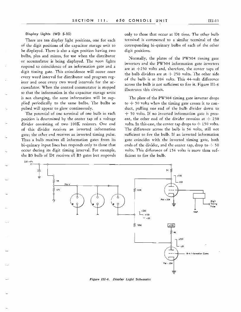
SECTION III.
Display Lights (WD 5-10)
There are ten display light positions, one for each of the digit positions of the capacitor storage unit to be displayed. There is also a sign position having two bulbs, plus and minus, for use when the distributor or accumulator is being displayed. The neon lights respond to coincidence of an information gate and a digit timing gate. This coincidence will occur once every word interval for distributor and program register and once every two word intervals for the accumulator. When the control commutator is stopped so that the information in the capacitor storage units is not changing, the same information will be supplied periodically to the same bulbs. The bulbs so pulsed will appear to glow continuously.
The potential of one terminal of one bulb in each position is determined by the center tap of a voltage divider consisting of two lOOK resistors. One end of this divider receives an inverted information gate; the other end receives an inverted timing pulse. Thus a bulb receives all information gates from its bi-quinary input lines but responds only to those that occur during its digit timing interval. For example, the B5 bulb of Dl receives all B5 gates but responds
250 volts
10K
206 V
47K
650 CONSOLE UNIT 111-11
only to those that occur at Dl time. The other bulb terminal is commoned to a similar terminal of the corresponding bi-quinary bulbs of each of the other digit positions.
Normally, the plates of the PW504 timing gate inverters and the PW504 information gate inverters are at +250 volts and, therefore, the center taps of the bulb dividers are at + 250 volts. The other side of the bulb is at 206 volts. This 44-volt difference across the bulb is not sufficient to fire it. Figure III-6 illustrates this circuit.
The plate of the PW504 timing gate inverter drops to + 50 volts when the timing gate causes it to conduct, pulling one end of the bulb divider down to + 50 volts. If no inverted information gate is present, the other end of the divider remains at + 250 volts. In this case, the center tap drops to + 150 volts. The difference across the bulb is 56 volts, still not sufficient to fire the bulb. If an inverted information gate coincides with the inverted timing gate, both ends of the divider, and the center tap, drop to + 50 volts. This difference of 156 volts is more than sufficient to fire the bulb.
lOOK
L SO -el50 +50
lOOK
NAP
. B-A Information Gates
PW - 504
Digit Timing Pulse
Figure 111-6. Display Light Schematic

III-12 IBM 650
There are two lights in the sign posItIOn (DO). The plus light fires when a Q4 information gate coincides with a DO timing gate. The minus light fires when a Q3 information gate coincides with a DO timing gate. This follows from the fact that a plus sign is stored in the distributor as a 9, while a minus is stored as an 8. The Q4 and Q3 information gates will be available at DO time only from the distributor or the accumulator sign latches, because there is no DO position in the program register.
CONTROL CONSOLE SWITCHES
Address Selection Switches WD 7-01
The address selection switches have two functions: 1. To set up a four-digit address that it is desired
to manually transfer to the address register. 2. To set up a four-digit address that is to be com
pared with the contents of the address register to develop an address stop signal when the two addresses are the same, if the control switch is in the address
stop position.
Address Transfer
The outputs of the 28 address register latches (WD 7 -00) connect to the binary and quinary sections of each address selection switch (WD 7-01). When a decimal value is set in a switch, the wiring is such that a circuit is completed between the binary and quinary common switch segments and those address register latches that represent the decimal value.
To transfer a number from the switches to the address register latches, the address is set in the switches. The control switch is set to MANUAL, and the transfer key is depressed. The following circuit is used to turn the proper latches on:
The address selection switches connect the diode cathodes, in units 15A, 15B, and 16A (WD 7-01C) to the selected address register latch outputs. N ormally the address register will have been previously reset by depressing the program reset key. Assuming no voltage drop in the diodes, the diode plates will be at the same potential as the address register latch outputs (about - 35 volts). Depressing the transfer key raises the diode plates essentially to ground potential; via the control switch set to MANUAL. Conduc-
tion of the diodes raises the connected latch output lines, through the address selection switches, to
ground potential. Reference to WD 7-00 will show that when any latch output line is raised to ground, the latch will be turned on through its latch-back diode.
Address Stop
With a specific address set in the address selection switches, all eight lines from the common segments will be raised only when the corresponding address register latches are on. When this occurs, all eight inputs to the switch at 15A, 15B, and 16A (WD 7-01C) are raised. If the control switch is in the AD
DRESS STOP position, this signal is sent through a double inverter and capacitor-coupled cathode follower. The resulting spike turns off the run latch.
Control Switch WD 7-01 C
The functions of this switch have been covered in connection with the address register and the address selection switches.
In ADDRESS STOP it allows an address stop signal to be developed when the address selection switch setting is matched by the address register latches and causes any reset of the address register to be to 8000 rather than blanks.
In RUN it also causes any address register reset to be to 8000.
In MANUAL it allows the transfer key to transfer a number from the address selection switches to the address register and causes any reset of the address register to be to blanks rather than 8000.
With the control switch set to MANUAL, the RUN
signal for the control commutator, and the run control cathode follower output are driven negative.
Master Power Off Switch (WD 7-02A)
This is a recessed toggle switch whose operation immediately cuts off all power to the machine. It is provided for use only as a safety measure and should not be used for normal machine operation, because it disregards the normal power on and power off operating sequences.

SEC T 1·0 N I I I .
Half-Cycle Switch (WD 7-01 C)
The action of this switch parallels that of the program stop key. Thus when it is in the half cycle position, the control commutator is stopped at the end of each restart word interval. Each depression of the program start key will allow it to advance until the next restart. Thus the machine may be manually halfcycled through program steps.
Programmed Stop Switch (WD 7-01 C)
When this switch is in the STOP position and an 01
operation code is sensed, the run latch is turned off, stopping the control commutator. This action was described under Program Light.
Error Stop-Sense Switch (WD 7-01 C and Figure 111-7)
This switch is provided to allow the use of selfcorrecting program routines. The machine can be made to respond to a detected error in either of two ways, depending upon the setting of this switch.
1. ERROR STOP. With the switch in this position, an error will cause the run latch to be turned off and the control commutator to be stopped at the end of the operation on which the error was detected.
2. ERROR SENSE. With the switch in this position, an error will turn the run latch off momentarily. Automatic program reset, accumulator, and errorreset signals will be developed, which will reset all units just as if the program, accumulator, and errorreset keys had been used. The address register will be reset to SOOO (because the control switch is in the RUN
or ADDRESS STOP position) and the run latch will be automatically turned back ON. The next instruction will be taken from the switches (SOOO) instead of the intended I-address, and the machine can branch into a self-correcting routine, if such a routine is provided
in the programming.
Error Sense
With the switch in this position, and after the error stop latch turns on, the circuits act as follows:
1. The error-sense latch is turned on and lights the error-sense light. This latch is reset only by a subsequent depression of the error-sense reset key.
2. Program accumulator, and error-reset signals are
650 CONSOLE UNIT
Mon. Ace.
Enor Stop Si,o Clodr:lng &ror All Re5tarts.D f« I (6-30) (1-30) . (7-3Oj
1-1 ___ + __ ----.JI
CF &ror Stop
+150 Error Disable Swilch Closed
EITOt Stop latch
+1,.
Stop Se~ -----ErrorStopSen5eSort, --
EI'fOfReset Mon. Envr
(7-30) -T\
III-13
Error ...... LlghtCF
..... " ... light 7-02
Error Hahn CF
Frog. Reset Resel (7 ... 21)
(7-02) \
L-________ ~.~----------~
(7·20) ± Tum on Iur. Latch (7-10)
Fil1ure 11l-7. Error Stop and Sense Function Chart
developed as a result of the signal coincidence at the switch at SG diodes 11, 12. These signals parallel the similar signals developed when the accumulator, program, and error-reset keys are used except that the error-reset signal from 4H pin S does not reset the error-stop latch because of the blocking effect of di~de 12 at 7e.
3. The run latch is turned off with the next EDOU gate by the switch at 7D diodes 1, 2, and the errorrestart latch is turned on by the switch at 3D diodes 6, 7. The error-restart latch remains on through its coincident latch back circuit until the next NEDXU.
The error restart latch is turned off with the next NEDXU. The resulting positive pulse from 3F pin 5 causes a spike output from the capacitor-coupled cathode follower, which is applied to the grid of the cathode follower at 7E. With the error stop-sense switch in the SENSE position, the cathode follower at 7E produces a positive spike to turn the run latch back on, and the error-stop latch off. The error-sense light remains on until the error-sense reset key is depressed.
Error Stop (Figure 111-7)
With the switch in this position, the output of the error stop latch is able only to turn the run latch off. The diode switch at sG diodes 11, 12 is blocked as are the cathode followers at 71 and 7E pin 6, 7, S.

III-14 IBM 650
Error Disable Switch (WD 7-30)
The error disable switch is a control console cover interlock switch that may be opened when the control console panel is swung out. It provides anode voltage for the cathode follower at 7E pin 10 and allows the output of the error stop latch to be used. Any detected error (except those that operate the storage check latch, WD 7 -OOAU) will cause the error stop latch to turn on.
Overflow Stop-Sense Switch
The functions of this switch were described under
Overflow Light.
Display Switch (WD 5-11 B)
The main function of the display switch is to select the accumulator (upper or lower), the distributor or the program register for display by the display lights. It also allows the control commutator to cycle continuously if it is in the upper accumulator, lower accumulator, distributor, or program register positions, but allows it only to cycle once in either of its manual operation positions (read-out storage or read-in storage). This switch also removes plate voltage from the general storage read-out latches in its read-in storage position to prevent a conflict of information on the selected storage line on a read-in storage operation.
The switch is a six-position switch with three sections. The third section supplies anode voltage to the upper accumulator, lower accumulator, distributor, or program register light selection cathode followers, depending upon its setting. Outputs from the accumulator on-time latches are switched with upper and lower word gates to provide inputs to the upper and lower light selection cathode followers. On-time outputs from the distributor and program register drive the distributor and program register light selection cathode followers. All these cathode follower outputs
are commoned and feed the bi-quinary, light selection output lines. The information on these lines then consists of on-time B-A information gates from the selected capacitor storage unit. These lines connect to terminals 2Ca, 2Bd, etc., on WD 5-11B. These terminals connect to CI0-3, CI0-2, etc., on WD 5-10C and are the information input to the display lights.
Notice that anode voltage is supplied to the distributor light selection cathode followers by either the distributor, read-out storage, or read-in storage positions of the switch. On a read-out storage operation, the contents of a storage location, specified by the number in the address register are transferred to the distributor and displayed from there. On a read-in storage operation the information set in the storage entry switches is transferred to the distributor and then to general storage.
In order for the control commutator to advance normally, a nl1Z signal must be available when the run latch is on, provided the display switch is in any position other than the two manual operation positions (read-out storage and read-in storage are both manual operations). WD 7-1 OAL shows that the ON output of the run latch raises the grids of three cathode followers, run control, manual read-out storage, and manual read-in storage. When the second section of the display switch is in the read-out storage posi
tion (WD 5-11B), + 150 volts is applied to C43-5, to 9Dz and the manual read-out storage. Cathode follower at 9E; therefore, when the run latch is on, it provides the manual read-out storage signal instead of the run signal. In the read-in storage position, + 150 volts is applied to C43-4, to 9Dw, and the manual read-in storage cathode follower at 9E. In this case, the run latch, when on, provides a read-in storage signal instead of the run signal.
On the read-in storage operation an 8000 control signal is developed by the manual read-in storage signal. This opens the path between the storage entry switches and the selected storage output line, allow
ing the storage entry switch information to enter the distributor. (The manual read-in storage signal also provides a R.I. distributor gate.) Meanwhile, the address register output has energized the general storage read-write matrix. Therefore, when a RIGS gate is provided, timed by the onc-ll/ord early selection circuits, the switch information (now in the distributor) is read into the selected general storage location.
Reference to the general storage read-write matrix circui ts (WD 4-10) will show that information is available from the selected band as long as a valid general storage address is in the address register. Normally this information operates the five general storage
SECTI·ON III.
read-out latches, supplying a stream of B-A information gates to the selected storage output line. If this is allowed to happen, there will be a conflict of information from entry switches and the general storage band on the selected storage line. To prevent this, the general storage information is blocked on a readin storage operation.
When the first section of the display switch is in the READ-IN STORAGE position (WD 5-11B), - 50 volts is applied from the control switch set to MAN
UAL to the switch at 4H (WD 4-00B). Therefore, the cathode follower outputs will be down, blocking the general storage latch output from reaching the selected storage output lines.
Storage Entry Switches (WD 5-10)
These switches provide a way to insert manually a word of information into any storage location. They are addressable (8000) and therefore may be used as a source of information by the program routine. As such they are used as the alternate source of an instruction word on self-correcting error program routines.
There are eleven switches, one for each significant digit of a word and one for the sign.
650 CONSOLE UNIT 111-15
Each switch has two sections, one for the binary level and one for the quinary level. Digit timing gates corresponding to the digit position represented are fed to the common segments of each switch. For a given decimal setting of a switch, digit gates will be distributed to the two bi-quinary lines that represent the digit. In the case of the sign position, a plus setting distributes a DO gate to the B5 and Q4 lines, while a minus setting distributes a DO gate to the B5 and Q3 lines.
These storage entry switch outputs are used either on a manual read-in storage operation or when the output of the address register is 8000. In the first case, a forced 8000 signal (heat 8000) is developed at terminal9Wz (WD 7-10CU) by the manual start readin distributor latch and is applied to C20-2 (WD 5-10C). In the second case, an 8000 address signal is developed at terminal 8Ea (WD 7-00BU) from the address register output and is applied to C19-2 (WD 5-10C). These signals are mixed at 16B so that either signal conditions the diode switches at 14B, 15A, 15B, and 16A. The storage entry switch outputs are thus gated through to the selected storage output lines by either an 8000 address or a heat 8000 signal from where they may enter the distributor or pro-gram register as the case may be. .


SECTION IV. ARITHMETIC UNITS
CAPACITOR STORAGE UNITS
THE PRINCIPLE of the basic capacitor storage binary
cell was discussed in Basic Principles (Section 2) under Capacitor Storage. In the 650, three major storage
units are built up from these basic cells: the distribu
tor, the program register, or program step storage unit, and the accumulator storage unit. Each of these
units is much the same in principle, although slight
differences exist in methods of read-in and regenera
tion control.
Distributor
Wiring diagram 6-10 show the circuits' comprising the distributor and its regeneration, read-in and reset controls. The unit consists of a capacitor storage ma
trix, even- and odd-digit amplifiers and blocking inverters, early latches, on-time latches, and pedestal
cathode followers together with entry switching and
read-in and regeneration controls. The matrix is made of eleven columns of seven
capacitor storage cells. There is one column for each digit storage position and one for the sign. There are seven cells in each column, one for each of the seven bi-quinary bits. The distributor is required to store
eleven digits, DO being the sign storage position. The seven cells of each column have their read-out
terminals common and driven by a one-digit-early
gate and their read-in terminals common and driven
by an on-time digit gate. The capacitor terminal of each of the even-digit
cells in a bi-quinary row connects to a common ped
estal line controlled by a pedestal cathode follower.
The same is true of the odd-digit cells.
For purposes of explanation assume that the distributor has been reset and is storing plus zeros. In this case, the DO position contains a 9 (only the B5 and Q4 capacitors are discharged). All other digit positions contains zeros only (BO and QO capacitors
discharged) .
IV-l
Distributor Regeneration
At DX time a B-A read-out gate is applied to the DO position. The B5 and Q4 capacitors charge, developing capacitor charge spik.es across the resistor in the corresponding pedestal cathode followers. These
spikes drive their corresponding even-digit amplifiers, which are free to operate because their blocking inverters normally conduct only during even-digit time intervals (DX is an odd-time interval). These amplifier outputs turn on the corresponding B5 and Q4 early latches. These latches stay on for the remainder of the DX interval and are reset by an inverted AP
through the associated reset inverters. The early
latches while on, furnish a distributor early output.
When the early latches go off at A time, the cor
responding on-time latches are pulled on by a pulse
from the left anode of the early latches through a capacitor-coupled inverter. These on-time latches are
held on until the next A time through a latch back circuit controlled by a NAP, and while on, furnish an
on-time output during Do time. The on-time latch outputs also switch with NAPs and (in this case) an even-digit gate to raise the B5 and Q4, even-digit
pedestal lines during DO time. This raising of the pedestal lines coincides with the DO read-in gate on
the DO position and allows the B5 and Q4 capacitors
to discharge on top of the pedestal as explained in Basic Electronic Circuits. The even-digit amplifier
blocking inverters are conducting during DO time while the even-digit lines are being pedestalled, thus preventing the amplifiers from responding to the ped
estal pulse and incorrectly turning on the early latches.
At the same time the D1 position (an odd position) is being read-out through the odd-digit amplifiers and
the foregoing process is repeated with read-out occur
ring at DO and read-in at Dl time. The BO and QO
latches will be active, because the BO and QO capacitors were discharged.

IV-2 IBM 650
Note the vacuum diodes connected between read-in and read-out lines of the capacitor storage cells. They clamp the pulsed output of the read-in inverters to
that of the read-out cathode followers (about + 10 volts) to stabilize the capacitor output spikes.
This processing reading out one digit early, reading in on-time and pedestalling two of the seven lines during read-in time from the on-time latches is repeated for each digit position. Each column of capacitors is tested once each word interval and thus is required to maintain its state of charge or discharge
for 96 microseconds. In this way a number stored in the unit is continu
ously available from the early and on-time outputs
and is continually regenerated. Reading a new number into the unit merely re
quires the circulating regeneration path to be opened and that two of the seven pedestal lines be operated each digit time by on-time pulses from the source of the information instead of pulses from t~e distribu
tors on-time output. This is accomplished by the distributor read-in and
regeneration controls. In the case of the distributor, regeneration is interrupted by causing the output of the regeneration control latch to energize all of the even- and odd-digit amplifier blocking inverters so that the outputs from the capacitor matrix cannot turn on the early latches. With the early latches blocked, the on-time latches cannot be turned on and regeneration is prevented. Instead, an output from either of the distributor read-in control latches (storage to distributor read-in or accumulator to distributor read-in) will open read-in switching, allowing the on-time latches to be turned on by on-time output pulses from either selected storage or the accumulator. When regeneration is interrupted by blocking the turning on of the early latches, it must be done by a gate that is one digit early with respect to the gate
that opens the read-in switching. WD 0-99 shows that the distributor can be read
into from two sources: 1. Selected storage that includes any general stor
age location, the storage entry switches (8000), and upper or lower accumulator when selected by an 8002 or 8003 address.
2. Directly from the accumulator on-time output
(Codes 20, 21, 22, 23).
The selected storage source is used to enter information into the distributor on all arithmetic operations (10' sand 60's codes). The first step of any arithmetic operation is the entering of data into the distributor from a storage location specified by the D-address of the instruction word. The data is then available from the distributor outputs for use in accomplishing the operation.
On 10's and 60's operations, a signal is sent from the program control commutator to operate the distributor read-in and regeneration controls. This signal occurs at DX time of the word when the storage location containing the data to be entered is in position to be read out.
To enter a selected word of information into the distributor, the distributor's selected storage entry switching must be open for Do through D 1 0 of the selected word interval and its regeneration path must be blocked from DO through D9 time. WD 6-10CU shows how the read-in distributor signal (DX) turns on the read-in distributor from storage latch and in turn the distributor regeneration control latch to provide the necessary read-in and regeneration blocking gates.
The read-in gate is actually open during DX .although not needed until Do time. No harm is done, however, because no output is available from any general storage location or the switches at DX time, and any DX output from the accumulator is a zero. A zero at DX time would only turn on the BO and QO on-time distributor latches, which are forced on at DX anyway by a distributor reset circuit, to provide an on-timG distributor output at DX to satisfy
the distributor validity check circuits. Regeneration is not blocked at the beginning of
DX time when the distributor's sign position is being read out because of delays between the development of the read-in distributor signal and the blocking inverters. Instead the Q3 and Q4 early-latches are held OFF every DX of a read-in distributor operation. The B5 early-latch is not held off; since in going off it turns on the B5 on-time latch at DO time. This causes no failure because the B5 on-time latch is
turned on at DO time anyway from selected storage. The read-in distributor from storage latch and the
regeneration control latch are turned off with a DIO
DP. Actually they taper off, because time is required

SECTION IV.
for a latch transfer, and cannot be considered fully down until the end of D10 time. Thus the read-in gate is up through D10 as required. The regeneration blocking gate is held through D 1 0 also although this would not be necessary, because no distributor posi
tion is read out at D10 time. Whenever a manual accumulator reset gate is de
veloped by depressing either the accumulator reset key or the computer reset key on the control console, the distributor is reset to plus zeros. This is done by holding the Q1, Q2, Q3 on-time latches off for all digits during manual accumulator reset; the B5, Q4 latches on and the BO, QO latches off for DO during manual accumulator reset; the BO, QO latches on and the B5, Q4 latches off for all digits except DO during manual accumulator reset. WD 6-10BU shows the switching of manual accumulator reset with DO and
NDO to accomplish this resetting.
Accumulator
The accumulator is a capacitor storage unit similar in principle and circuitry to the distributor and the program register except that it has capacity for two words of storage. The lower accumulator has twelve storage positions, DXL, DOL and D1L through D10L positions. The upper accumulator has 10 positions, DIU through D10U. There is a two-digit time gap
between the D 1 oL and DIU positions, because there are no DXU or DoU storage positions.
The accumulator (WD 6-00) consists of a 22-digit capacitor storage matrix, even- and odd-digit amplifiers and blocking inverters, early latches, on-time latches, read-in and regeneration switching, pedestal cathode followers and reset controls. Stored information is continuously regenerated as long as the accumulator regeneration gate is up. As with the distributor and program register, regeneration is accomplished by allowing the on-time latch outputs to
control the pedestal cathode followers. All read-in to the accumulator is to the pedestal
cathode followers. During the read-in operation the following controls are operated: Accumulator regeneration is turned off, opening the circuit between on-time latches and pedestal cathode followers. Accumulator read-in is brought up, completing the circuit between adder output and pedestal cathode
followers. The adder output now replaces the on-time
ARITHMETIC UNITS IV-3
latch output and read-in from the adder takes place. It is also possible to control the pedestal cathode
followers from the accumulator early latch outputs. This is done when the accumulator regeneration gate is turned off and the right-shift gate is developed. This is used to accomplish a right-shift operation.
The accumulator regeneration, accumulator readin, and right-shift latches that develop the read-in and regeneration control gates are part of the arithmetic control circuits and thus are not shown with the accumulator.
The accumulator is read into during the execution of the following codes: 10, 11, 14, 15, 16, 17, 18, 60,61,64,65,66,67,68 (add, subtract, multiply and divide operations), 30, 31, 35, 36 (shift operations), 84 (TLU). Arithmetic controls for each of these operations will therefore operate the accumulator regeneration latch and accumulator read-in latch. Codes 30 and 31 will also use the right-shift latch.
The operation of these control latches will be discussed later in connection with the description of the specific operation.
Several special circuits, not found in the other capacitor storage units are associated with the accumulator to handle conditions arising because of its design and use. These circuits will be discussed in the following paragraphs.
Because there are no DXU and DOU accumulator positions, the DIU position is read out at D10L time (one accumulator digit position early). DIU cannot be read-in until DIU time. The early latches, therefore, must not be reset during DXU and DOU time. To accomplish this the A pulses, which control the early latch reset inverters, are switched with a negative D10cL-DOcU gate. (Negative digit 10 clower to digit 0 c upper). This is a gate that is up for A time of all digits except DXU and DOU. Thus A pulses are supplied to reset the early latches except at DXU and DoU times.
On all operations requiring an accumulator entry to the adder, except the left-shift codes (35 and 36), the accumulator early output is used. On these operations therefore, the DIU information contained in the early latches is presented to the adder for three successive digit time intervals, D10L, DXU, and DOU. It will be seen later, when the adder circuits are described, that the adder does not accept this informa-

IV-4 IBM 650
tion for analysis until DO time. Reset of the adder
carry latches is prevented during DXU and DOU time so that their carry or no-carry information setup from
the DI0L digit is still available at DOU time for use with the DIU information to provide the correct
result.
Because of the lack of DXU and DOU positions and
of the previously mentioned behavior of the early latches during DXU and DOU time, there is no normal input to the on-time latches at DXU and DOU
times. To satisfy the validity check circuits an on
time DXU and DOU output of zero is created by forcing the BO and QO on-time latches on with DXU
and DOU gates. This is accomplished through the mix
circuit inputs to these two latches (WD 6-00CU).
On reset add or subtract operations it is necessary
to disregard the number that may be in the accumulator and to merge, in the adder, the contents of the
distributor with zeros substituted in place of the con
tents of the accumulator. This result is then stored back in the accumulator. The number in the distributor has been placed in the accumulator and the effect of an add or subtract with reset has been accom
plished.
On manual accumulator reset operations a manual
accumulator reset gate is produced by depression of either accumulator reset or computer reset keys on
the control console. This forces zeros into the on-time latches for each digit during the full two accumulator word times. These on-time latch zeros are regenerated into the matrix, thus resetting the accumulator.
The DOL position of the accumulator is not used
for storage of the sign. Each time a number is entered into the accumulator, its sign is determined and
held in the accumulator sign latches. The output of
these latches helps to determine whether the next accumulator entry to the adder will be true or comple
ment. The output of these latches also causes either a bi-quinary 8 or 9 to be inserted into the accumu
lator on-time output lines at DO time for transfer
to the distributor.
The DOL position is used on multiply, divide, and shifting operations to hold the shift count number.
The DXL position is used on multiply and divide to store the high order digit of the multiplicand and
the high order digit of the dividend.
ADDER
FIGURES 1-11 and WD 0-99 show how the adder and its A and B entry switching fit into the machine's data flow arrangement.
The adder is used in the accomplishment of all
arithmetic operations (1 O's and 60's except 69), the shift operations (30's) and the table-lookup operation, 84). There are two, 7 -bit, bi-quinary input
lines, and one 7 -bit, bi-quinary output line a~sociated with the adder. Bi-quinary digit information is pre
sented to the adder simultaneously on each of its two inputs. The bi-quinary sum of the digits presented is available from the output.
The information entering the adder is presented
digit by digit, from any of the several serial storage sources that have data flow paths connecting their
outputs to an adder input. The selection of the source
of information to be presented and the time of presen
tation to the adder are the functions of the A and B
input switching circuits. These circuits are opened and
closed, thus gating information to the adder, by con
trol gates developed by the program control and arithmetic control circuits.
A delay of one digit time is incurred in the adder; i.e., the sum of two digits is available from the out
put one digit time after they have entered the inputs.
The design of the adder is such that information must be presented simultaneously at the two inputs to obtain an output signal.
Bi-Quinary Arithmetic
The 650 adder uses only the operation of addition to accomplish all calculations. Subtraction is achieved
by entering one of the two numbers as a complement. Multiplication is done by over and over addition of the multiplicand. Division requires repeated subtraction of the divisor from the dividend. Thus
the serial, one digit adder need only have the ability
to receive two simultaneous, bi-quinary indications of digit values; combine them with a stored carry or
no-carry indication from the preceding digit analysis,
and produce a bi-quinary indication of this result.
Figure IV -1 is an example of a bi-quinary addition and subtraction operation with decimal comparison.

SECTION IV. ARITHMETIC UNITS IV-5
ADDITION
12345 + 67890 = 80235
Bi-Quinary System
05 04 03 D2 DI
Decimal System B Q B Q B Q B Q B Q
05 04 03 02 01 Above 5 5 5 5
Corry I I I Corry I 1 1
Adder entry A 1 2 3 4 5 Adder entry A 0 I 0 2 0 3 0 4 5 0
Adder entry B 6 7 8 9 0 Adder ehtry B 5 , 5 2 5 3 5 4 0 0
Adder Output 8 0 2 3 5 Adder Output 5 3 0 0 0 2 0 3 5 0
Decimal System
D6 D5 D4
Corry 1
SUBTRACTION
80235 - 67890 = 12345
D3 D2 DI Above 5
1 1 Corry
B
5
B;-Quinary System
D6 D5 D4 D3 D2 D1
Q B Q B Q B Q B Q B Q
5 5
1 1 1
Adder entry A 0 8 0 2 3 5 Adder entry A 0 0 5 3 0 0 0 2 0 3 5 0
Adder entry B 9 3 2 1 0 9 Adder entry B 5 4 0 3 0 2 0 1 0 o 5 4
Adder Output 0 1 2 3 4 5 Adder Output 0 o 0 I 0 2 0 3 0 4 5 0
Figure IV -1. Bi-Quinary Addition and Subtraction
NOTE: On all additions involving a complement, a carr)' is inserted in the units position.
The digits to be added are presented in bi-quinary form. Each decimal digit is represented by simultaneous B-A information gates on two of the seven
bi-quinary lines, one gate on one of the lines of the
binary level, and one on one of the lines of the quinary level. The quinary levels are added. In the quinary (base 5 level) the only values possible are 0, 1,
2, 3 and 4. Whenever a quinary sum exceeds 4, a
carry into the binary level occurs, the quinary returns
to 0 and again begins to advance toward 4.
Each of the two positions in the binary level represents a count of five units. That is, the two binary in
dications alternate to show whether the value represented by the quinary level is below five (0, 1, 2, 3, or 4) or five and above (5,6,7,8,9). Because the
binary level counts in units of five, any carry from the
quinary level to the binary will be a five-unit carry.
Similarly, because the quinary level counts units of
one, any carry from a binary level to the quinary of the next digit will be a one-unit carry.
Subtraction is accomplished by adding the complement of the number to be subtracted. In the binary
level BO and B5 are complementary, while in the qui
nary level QO and Q4 are complementary as are Q1 and Q3. Q2 is its own complement. The fact that the two levels are diagonally complementary as shown in Figure IV -2, makes complement entries to the adder quite simple. It is necessary only to allow the information gate from the source to enter the adder on the
diagonally opposite adder input lines. The result is the entry of a 9's complement. However (as indicated in the preceding subtraction example, a carry indication is inserted into the adder so that its analysis of
the units digit is the same as if a carry had been left
over from a preceding digit. This is done on any complement entry and the effect is the same as if a
10's complement had been entered.

IV-6 IBM 650
Adder A and BEntry Switching
WD 0-99 shows the different data flow paths, mix
ing at adder entry switching A, anyone of which
can supply information to the adder A input lines and the different paths mixing at entry switching B
that can supply information to the B input lines. The
details of these A and B entry switching circuits are
shown in WD 8-00 and WD 8-20. The control gates are developed by the arithmetic control circuits in ac
cordance with the operation being executed. The de
velopment of these control gates will be discussed in a later section on arithmetic controls. Thus, for any
given arithmetic operation the control gates will se
lect the data flow paths and will open these A and B
switching circuits at the proper times and for the
necessary intervals to supply information to the adder
as required by the operation.
Adder Circuits The one-digit adder consists of diode switch and
mix circuitry, carry and no-carry latches, binary and quinary output latches, reset controls, carry and nocarry insert controls and adder output latch zero
insert controls. In effect bi-quinary addition tables are built into
the adder. For a particular pair of bi-quinary inputs
only one bi-quinary output, which is the sum of the
inputs, is obtained.
During a digit interval when information is presented to the adder two of the seven bi-quinary input
lines, at both A and B inputs, are raised (WD8-10).
Either the carry or the no-carry latch will be on as
a result of the preceding digit analysis or as a result of a carry or no-carry insert. Quinary inputs are
analyzed in the quinary matrix. Similar A and B
quinary inputs are mixed to give A or B QO, A or
B QI, A or B Q2, A or B Q3, or A or B Q4 signals
from the cathode followers so labelled. When the A
and B quinary inputs are not the same, two of these
cathode followers will be energized. All combinations
of two of these five cathode followers are switched to operate the quinary sum cathode followers and indicate a quinary sum of I, 2, 3,4, 5, 6, or 7. When
the A and B quinary inputs are similar they are also switched, and mixed where necessary, to operate the quinary sum cathode followers and indicate a quinary
sum of 0, 2, 4, 6, or 8.
The 0, I, 2, 3 and 5, 6, 7, 8 quinary sums are sep
arately mixed to give below- 5 or 5 -and-above inputs to the binary matrix. The Q4 sum is switched with carry and no-carry signals. These switch outputs are
separately mixed into the below-5 and 5-and-above cathode followers. Thus a Q4 sum and no-carry is
below 5 while the Q4 sum and a carry is 5-and-above. The quinary sum signals 0 or 5, 1 or 6, 2 or 7 and 4 or 8 are mixed to provide the five signals for operation of the quinary output latches. These signals are
all separately switched with carry or no-carry D pulse signals to turn on the quinary output latches.
The three pieces of information necessary for turning on a quinary latch are quinary A input, quinary B input, and carry or no-carry. They are available during the adder entry digit interval and are sampled at the end of this interval with a D pulse. Thus, during D time of the adder entry digit interval, coincidence
of signals exists at one of the quinary latch input
switches. This positive D pulse output from the
switch is inverted to a negative D pulse and applied
to the grid of a capacitor-coupled inverter that is
normally cut off. A negative output is required from
this inverter to pull the latch on. Thus, the latch is turned on not during signal coincidence but when
coincidence is removed. This happens with the be
ginning of the next digit interval as the D pulse and the input and carry or no-carry signals terminate.
Signal coincidence was established and then removed from one of the latch input switches, which caused the latch to turn on.
Any adder latches that are on (binary, quinary and
carry or no-carry) are reset at A time of every digit
interval as long as the adder reset control latch is not
on. This reset is done by removing coincidence from the latch back switches with negative A pulses. Whenever it is desired to prevent resetting these latches, the adder reset control latch is turned on. Its output mixes to shunt the negative A pulses and holds the
reset line up. The time constant of the capacitor-coupled inv~rter
grid circuit is sufficient to supply a latch pull-on pulse
of about 4 microseconds duration. As just explained,
this pulse is acting to turn the latch on during the time that the NAP is re&etting the latches. However,
because the inverter pulse is of longer duration than the NAP, it overrides it, holding the latch on during

BO
B5
SOURCE OF
INFO. 00
01
02
03
04
COMPLEMENT ENTRY
CONTROL GATE
SECTION IV.
BO
B5
00
ADDER 01
02
03
04
Figure IV-2. Bi-Quinary Complement Entry
the NAP reset time and allowing it to latch back once the latch back circuit is completed at the termination of the NAP.
In this way, information that enters the adder during a given digit time is analyzed, combined with a carry or no-carry indication held over from the preceding digit, and transferred to the output latches at the beginning of the next digit interval. This information in the adder latches is available during the remainder of this next digit interval, for transfer to the accumulator, etc.
The information contained in the carry and nocarry latches, regarding the carry or no-carry status of the preceding digit, is used to set up the quinary latch for the next digit at the time when the sampling D pulse terminates. The carry, no-carry latches are, therefore, free at A pulse time, to be reset and set up with new information regarding the carry status of the new digit.
Returning to the adder entry terminals-at the same time that the quinary matrix is being energized by the quinary A and B inputs, the binary matrix is also energized by simultaneous binary A and B inputs. Four pieces of information must be analyzed to determine properly the binary sum and the carry, no-carry condition to be stored for the next digit. These con-
ARITHMETIC UNITS IV-?
ditions are: adder entry A, adder entry B, below-5, or 5-and-above, and D pulse. Figure IV -3 contains all the possible combinations and outputs. The below-5 and 5-and-above signals are a result of the quinary analySIS.
Entry Entry A B 5 and Above Below 5 DP OUTPUT B5 BO above 5 DP BO COrry BO B5 above 5 DP BO Corry B5 B5 above 5 DP B5 Corry BO BO above 5 DP B5 No Corry B5 BO below 5 DP B5 No Corry BO B5 below 5 DP B5 No Corry B5 B5 below 5 DP BO Corry BO Bu below 5 DP BO No Corry
Figure IV-3. Binary Addition Table
The input circuits to the binary latches and the carry and no-carry latches are energized in the same way that the quinary latches were energized.
The quinary latches and binary latches contain the new digit. The new-carry or no-carry indication is stored in the carry or no-carry latches. This new information is available from these latches during the remainder of the next digit interval.
As explained, three input signals are required to energize the binary matrix: a binary A input, a binary B input, and a 5-and-above or below-5 input from the quinary matrix. If anyone of these three inputs is blocked, there will be no output from the binary matrix to alter the status of the binary latches or the carry and no-carry latches.
If the blocking inverters associated with the 5-andabove and below-5 amplifiers are caused to conduct, they will block entry of the 5-and-above or below-5 signals to the binary matrix and thus prevent an output signal. This will prevent the status of the carry and no-carry latches from being altered.
This blocking action is used on those occasions where it is desired to prevent the normal resetting of the adder. When the adder reset control latch is turned on, not only is the NAP reset blocked as previously explained, but also the 5-and-above and below-5 blocking inverters are energized by the output of this latch. The carry and no-carry latches are thus protected so they will still contain the carry-no-carry indication of the last digit analyzed, even though several digit intervals pass before analysis of the next digit.

IV-8 IBM 650
The switch circuitry controlling the adder reset control latch is arranged to turn the latch on from DIObL-DOcU on any operation other than left shift or table lookup. On a left shift operation the latch is turned on from DXbU-DlcU, and on a TLU operation it is prevented from turning on at all.
The need for these adder reset controls is brought about by the two-digit gap in the middle of the accumulator at DXU and DOU. On all arithmetic operations except TLU the accumulator must supply its two words of information to the adder. On all of these operations except left shift the accumulator early output is used. On left shift the on-time out
put is used. When the accumulator early output is used to sup
ply the adder, the information to be analyzed must be presented to the adder one digit time early, so that an on-time output will be available from the adder
for storage back in the accumulator. It will be recalled from the discussion of the accumulator that the Dl U position is read out at DIOL time, and this information is stored in the accumulator early latches, which are not reset un til D 1 a U time. Thus, the DIU information is actually read out three digit times early but is still available for presentation to the adder at the normal one-digit early time, DoU. When this Dl U information is accepted by the adder at DOU time, the carry or no-carry information from DIOL must still be available for use by the adder in properly analyzing the DIU information.
This information will still be available in the adder carry, no-carry latches if they have not been reset and have not received any new signal. This blocking of any possible alteration of the carry status is accomplished by the Lt Sh Off control of the adder reset control latch.

SECTION V. FUNCTIONS OF OPERATION CODES
10'5 AND 60'S CODES
IN CONCEPT, the control commutator can be thought of as a two-branched ring (Figure V-I).
As an example of the operation of the control commutator, assume a series of instructions such as
XX XXXX 0012 10 0018 XXXX
During an I half cycle, the function of the control commutator is to
1. Find the location 0012 on the drum and read into the program register the instruction 10 0018 XXXX.
2. Signal that the new instruction has been read into the program register in order to cause a D half cycle.
During the D half cycle, the control commutator
sets up circuits that accomplish the following: 1. Find the location 0018 and read the data from
0018 into the distributor. 2. Perform the instruction 10 (add upper) using
the data in the distributor. 3. Signal that the operation 10 has been set up in
order to cause another I half cycle.
In the two-branch ring illustrated schematically, the amount of time necessary to complete each ring must vary. The cyclical nature of the 650, in which instruction and data words may be in any of 50 locations around the drum, makes necessary a flexible control system. Thus, after an I half cycle is started, its length depends on the location of the new instruction. Similarly, the length of a D half cycle varies
0 @
1 I Half Half 1 Cycle Cycle
0 ® .. 4
Starting Position
Figure V -1. Control Commutator
V-1
according to the location of the data and the type of operation being performed.
Another factor in the operation of the control commutator is the somewhat different operation for different operation code numbers. The 650 operation codes can be divided into the following groups:
00, 01 N o-op and STOP codes 10's and 60's Arithmetic codes 20's Store codes 30's Shift codes 40's and 90's Test codes 70's Input-output codes 84 TLU
The action of the control commutator is the same on the I half cycle for all of these groups. On the D half cycle the method of operation varies with the operation code. Control commutator principles and circuits will first be described in detail for a 10 code (add upper) operation. Later, the operation of the control commutator will be described for the other groups of codes.
Control Commutator
Before studying commutator operation, the student should be familiar with the operation code register, address register, program register, and distributor.
I HALF CYCLE (Figure V-2)
Major Objective:
Enter the next instruction word into the program register.
Minor Objectives:
1. Reset operation code and address registers. (Re
start A). 2. Transfer next instruction address (Dl through
D4) from the program register to the address register.
(Restart B). 3. Search for the next instruction word.
a. I Control b. Enable Read-In c. Start Read-In
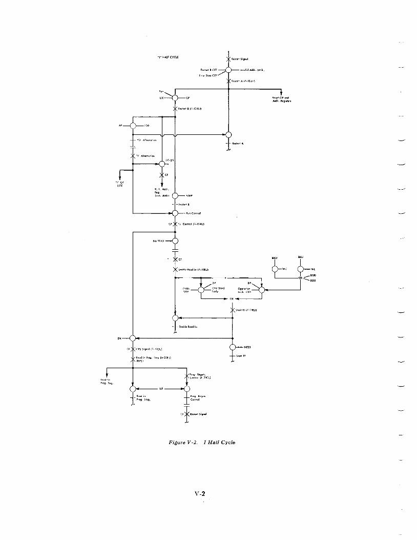
Read-In P,og. Reg.
AP--( (DO
"D" AlIe.nol;on
"I" OF UTE
"I" AII",.nolion
01-05
CF
R, I. Add.,
r~,IOrl 8 OFF
["0' :;109 OfF
cr
P~llo'l B (/-IQAI))
CF
Engble Read In (7-108U)
0000_
1999
09
On"wo.d Early
09
Ope'Qlio.. Inllk. OFF
'----... O. _------'
ox
£ngbl" R,,<!d In
CF RIPS Signal (7-1OCU)
Read in Prog. Slep (6-20SU) (RIPS)
~-----wp----~~
Read in ?og. Step,
P'og. Regen. CcrotrQl (6-2OCU
Prog. Regen Control
Figure V-2. I Half Cycle
V-2
Rl'selOParod Add" /lcgille.,

SECTION V. FUNCTIONS OF OPERATION CODES V-3
4. Read instruction word into the program register.
a. Stop program register regeneration
5. Restart signal to start the D half cycle. Figure V -3 shows the commutator operation for a
specific set of program steps. With this set of program steps, the word time at which each latch operates is predetermined. During word times 0011, 0012, and 001 3, the I half cycle occurs.
The following circuit elements function on every I half cycle.
Restart A
The restart signal to turn on restart A can occur at any digit time and at any word time, dependent only on the operation code being performed on the previous D half cycle. In Figure V - 3, it was assumed that restart A was turned on during word time 0010. The function of the restart A is to reset the operation code register and address register and to store the restart signal so that the restart B latch can be turned on at the beginning of the next word time.
Restart B
The restart A latch being on at the start of any word time will result in turning on the restart B latch. The purpose of restart B on an I half cycle is to cause the I-address of the instruction in the program register to transfer to the address register.
Enable Read-In
As soon as the I-address of the instruction III the program register has been placed in the address register during restart B time, the output of the address register attempts to develop a one-word-early D9 gate. If the I-address is 0013, one-word-early D9 would occur during 0012 word time. In order for the one
word-early D9 gate to be recognized, it is necessary to turn on an enable read-in latch. This latch must be on a minimum of one word time, if a drum address is in the address register. It could be on as long as 50 word times if the drum address of the example were 0012 instead of 0013. The example illustrates optimum programming, because the enable read-in latch is on for only one word time. Enable read-in is turned on when restart B goes off.
Start Read-In
The next step in the sequence of operating the RIPS gate is to turn on the start read-in latch. This is done at D9 time whenever enable read-in is on and a oneword-early D9 gate is developed.
Read-In Program Step
Whenever the start read-in latch is on at DX time during an I half cycle, a read-in program step signal will be developed. This signal turns on a latch that remains on for one word time so that the contents of drum location 0013 may enter the program register.
Circuit Description of the Alternation Control Latches (WD 7-10)
Assume that the D alternation latch is to be turned off, and the I alternation latch is turned on.
The restart B output switches at 9C diodes 1, 2, 4 with a EDO AP to provide a pulse to turn off the D alternation latch, and turn on the I alternation latch
so that an I half cycle can take place. The EDO AP output at 9C pin 3 is inverted by an IN503 unit at 9B. The negative pulse output then breaks the latch back of the D alternation latch at 11 G diodes 11, 12.
When the D alternation latch goes off, a capacitycoupled positive pulse from pin 7 of 11 H turns on the I alternation latch. The capacity-coupled input pulse to the I alternation latch lasts longer than the EDo AP to the latch back at IIG pin 6. The I alternation latch stays on until another restart B signal allows the control latches to again reverse their status.
D HALF CYCLE 10'$ AND 60'$ CODES
(Figure V-4)
As IS indicated by Figures V -2 and V - 3, the completion of the I half cycle when the RIPS gate ends, results in the restart signal, which initiates a D half cycle.
Major Objectives (Figures V-3 and V-4):
1. Search for the data 2. Perform the operation
Minor Objectives:
1. Reset operation code and address registers 2. Transfer operation code and data address (D5
through D 1 0) from the program register to the operation register and address register respectively.
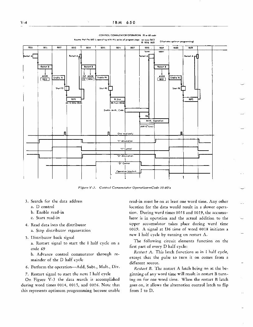
V-4 IBM 650
CONTROL COMMUl"TOR OPERATION, 10 Of 60 code
Au~ that the 650 is operating with this s.erie, of program ~teps: )01 xxxx 0013 10 0016 0021 (llIvstrotes optimum progromrntng)
0010 ()('II 0012 0013 0014 0015 001~ 0017 0018 0019 0020 0021
"We< 1 lower
RestartAL ReUort A Restott A r-- R •••• ,." i :-
Restort B Restart a Restort B
"OlR L"L "L ~ Enoble RI [!Q)[@D Enoble RI
~ Enoble RI
Start RI ~ ] Stort RJ S •• " RI
~ RIPS RIDisl RIPS
(RI 10 0016 0021) (RI f,om 0016)
Enoble Arj'h. Code.
06
Arith. Operation
Add to lower
n n One' word ear I y n I I "I" AItLno'ion J L-
"1"L".,ol -I II "0" Alternation I I
I ~D" Control II
I OPE"otion In'E"ti"ck I
I Figure V-3. Control Commutator Operation--Code 10-60's
3. Search for the data address a. D control b. Enable read-in c. Start read-in
4. Read data into the distributor a. Stop distributor regeneration
5. Distributor back signal a. Restart signal to start the I half cycle on a
code 69 b. Advance control commutator through re
mainder of the D half cycle
6. Perform the operation-Add, Subt., Mult., Div.
7. Restart signal to start the next I half cycle On Figure V -3 the data search is accomplished
during word times 0014, 0015, and 0016. Note that this represents optimum programming because enable
read-in must be on at least one word time. Any other location for the data would result in a slower operation. During word times 0018 and 0019, the accumulator is in operation and the actual addition to the upper accumulator takes place during word time 0019. A signal at D6 time of word 0018 initiates a new I half cycle by turning on restart A.
The following circuit elements function on the first part of every D half cycle:
Restart A. This latch functions as in I half cycle, except that the pulse to turn it on comes from a different source.
Restart B. The restart A latch being on at the beginning of any word time will result in restart B turning on for one word time. When the restart B latch goes on, it allows the alternation control latch to flip from I to D.
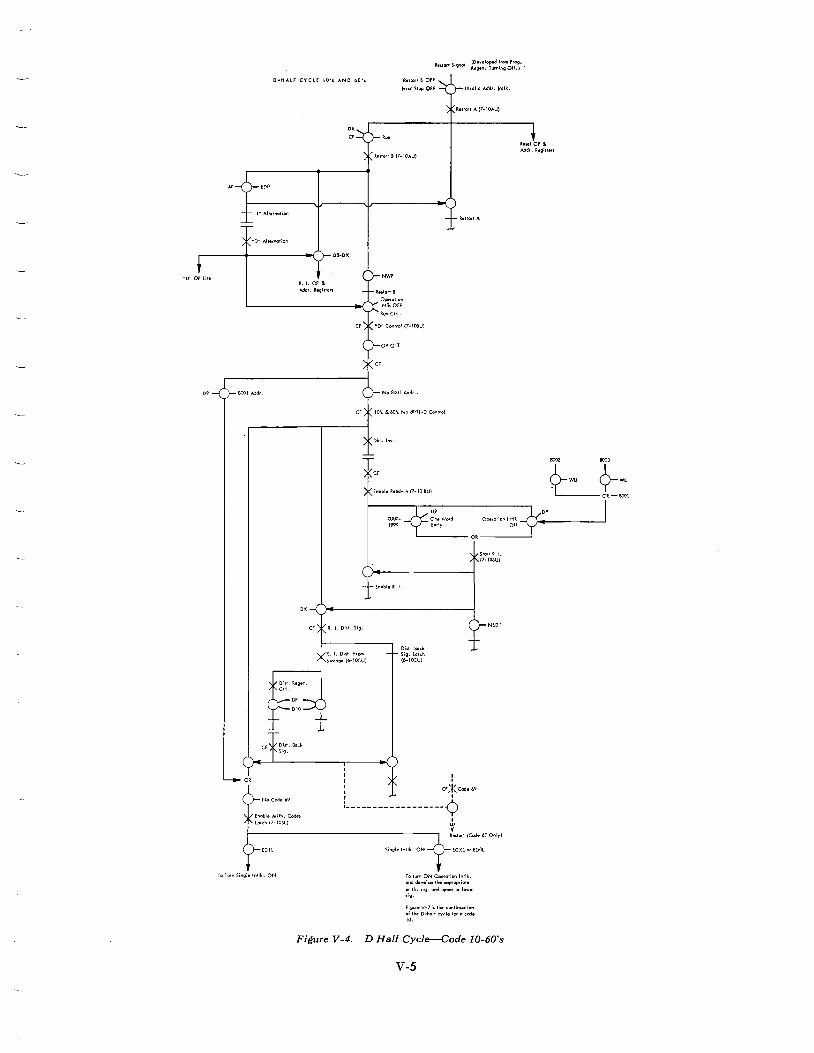
"0" OP Ute
09
O~HALF CYCLE 10', AND 60', •• llad B OFF
trror$'gpOFF
"0" Alt.,"II"o"
8001 Mdr.
OR
Til Turn 5ingle In!lk. ON
O!i-OX
R. I. OP & Add •. Regi,tel1
CF
CF
Rell".! B (7-IOAUl
CF
Ope'lIlion Intlk OFF
Run Ctrl.
opalT
No BOOI Add •..
Enllbl. Reod-In (7-10 BU)
0000-
"" D, O~e wo.d
Invalid Addr. Intlk.
Reitllr. A
Opera"on Inllk
0"
Re.eIOP & Add •. Rellil""
~--------o,--------~
I I I
Enoble ~ I.
Di.1. Blick 5'g. Latch (6-1OCU)
: CF:K Code 69
L _________________ ¢ I
"' V
Sta,'R.1. (7-10BU)
NEOI
Re,to.1 (Code 69 Only)
Single Intlk. OFF EOXl "r EDOl
To turn ON Ope.otion Intlk. and develop the app.opriate
arith .• ig. lind upper or lowe. lig.
FigureV-7il the continvatiOf"l of the D-halfcyc:le for II code 10.
Figure V-4. D Half Cycle-Code 10-60's
V-5

V-6 IBM 650
D Alternation and D Control. When restart B goes on, the alternation control latch, which had been at I is flipped to D. As restart B goes off, D control is turned on. The D alternation latch being on makes possible the read-in of the operation code and the naddress into the operation code register and the address register during restart B time. Also, the fact that D control is on allows the enable read-in, start read-in sequence to result in a read-in distributor signal instead of a read-in program step signal as on the I half cycle. The development of D control initiates a circuit to test the operation code. Refer to Figure V -3 to see the timing of D control and D alternation.
Enable Read-ln. As soon as the n-address of the instruction in the program register has been placed in the address register during restart B time, the output of the address register attempts to develop a oneword-early D9 gate.
In the example, one-word-early D9 occurs during word time 0015.
Start Read-ln. As in an I half cycle, the enable read-in latch output switches with a D9, one-wordearly D9 and no 800X address to turn on start readIn.
Read-In Distributor. Whenever start read-in is on at DX time during a D half cycle, the read-in distributor signal will be developed. The read-in distributor latch turns on for one word time so that the contents of location 0016 may enter the distributor.
The following circuit elements function on the second part of every D half cycle:
Distributor Back Signal. The distributor back signal, which occurs as the distributor regeneration controllatch goes off after the new data have entered the distributor, causes the control commutator to advance through the remainder of the D half cycle.
Enable Arithmetic Codes Latch. This latch causes the operation code to be examined and forces the 650 to wait for a lower word time before allowing the accumulator to go into action. The enable arithmetic codes signal, which is developed from the enable arithmetic codes latch, switches with the output of the operation code register to develop an add signal and an upper signal so that the add upper instruction will be performed.
Arithmetic Operation Latch. The development of an add signal (on a 10 or 60 code) will result in turning on the arithmetic operation latch. Once on, this latch controls the restart signal to signal the 650 to begin the next I half cycle. Also, interlock circuits are operated to prevent another accumulator operation until the present one is completed.
The arithmetic and shift operations make use of the accumulator and distributor and may require several word times for their completion. The restart signal on these operations is developed during the first word time of the operation. Thus, the commutator can advance concurrently with the performance of the operation and allow the next instruction to be located and read into program step storage. A restart for the D half cycle and a transfer of the new operation code and the n-address to the operation and address registers can take place. At this point, further advance of the commutator cannot be allowed until the preceding operation is completed.
Single interlock (WD 7-1 OCL) turning on prevents more than one testing of the operation code.
Operation interlock (WD 7-10CL) turning on prevents the development of a second D control until the accumulator and distributor have completed their operation. Operation interlock also prevents the development of a start read-in signal if the address is 800X. When an arithmetic or shift instruction has an 800X I-address, the locating of the next instruction must be prevented until the preceding operation is complete, because the instruction itself is in the process of being developed by the operation.
Code 69 (Load Distributor) (Figure V-5)
Major Objective:
To read the contents of the n-address into the distributor.
Circuit Operation:
The action is similar to the 10's and 60's code D half cycle except that only the enable read-in, start read-in sequence is performed. Energization of the enable arithmetic code latch is blocked and the distributor back signal causes a restart to I signal. Note that an operation code of 69 will always be accompanied by a p.o 8001 acldress.

Run
DX CP
Restart Signal (Developed from Prog,
Regen turning Off)
Restart B Off Inval ;d Addr Intlk
Error Stop Off Restart A (7-10 AU)
Re,tart B (7-IOAU) Reset OP and Addr Registers
AP
DS-DX
R.I. OP & Addr Reg.
"D" OP lite
OR
Dist. Regen Control (6-10 CUi
DX
Dist. Back Signal
~NOCOde 69
.: :: Enable N;th Code, (7-10 Bl) .. ~ (Does not turn ON for a Code 69)
OP 011
R.I. Dist. Signal
R.I. Dist. from Storage (6-10 CUi
Restart A
10·, & 60·s No 800I-D Control
Enable R.I.
Did. aack Signal later. (6-10 CUi
D9 Operation Intlk Off
One Word Early
OR_-----'
Start R.I. (7-10 BU)
NEDI
Restart Signal for next I-Half Cycle
Figure V-So D Half Cycle-Code 69
V-7

Add Signa'
Adder Entry { Ace. T.A. Gate "A"
Ae:e:. T .A. or Camp
{
adY Dht. Z.ro Con"ol
Adder Entry Early Dist. .. B II ZerO' Entry
Dist.T .A. Gate
No-Carry Insert
Carry Blank
Zero Insert
Ace. R.I. Gate
Ace. Regen
Restart
X 0 1 2
--I--.....
3
Plus DidributOf' and Plus. Accumufotor
Ae:e:. True
Add Gote (8-30 DU)
Low.r
4 5 6
-~
7 8 9 10
I-
02
X 0
Figure V-6. Add Upper-Code 10
V-8
Adder ( 8-10)
, , ,
! No-Corry Corry Blonk~ Insert ( 8-30 EU) I:,
(8-30 EU) , ....... _ ••••••••• _.~_~_ •• _. __ J
Ace. Read-In Got. (8-30 CU)
: Early Dlst, -----+i : Zero Entry ! (8-318U)..-_ ........ -,
i Early Dist. : Zero Control , (8-31 8U)
i Adder Entry "8" ( 8-20)
Dlst. True
Add Got. 18-30 CL)
1 .. ___ .... _-------- .. _---- .. -_ ... _---------_._-_ .... _ ...... -.
Upper
1 2 3 4 5 6 7 8 9 10
.....
Ir
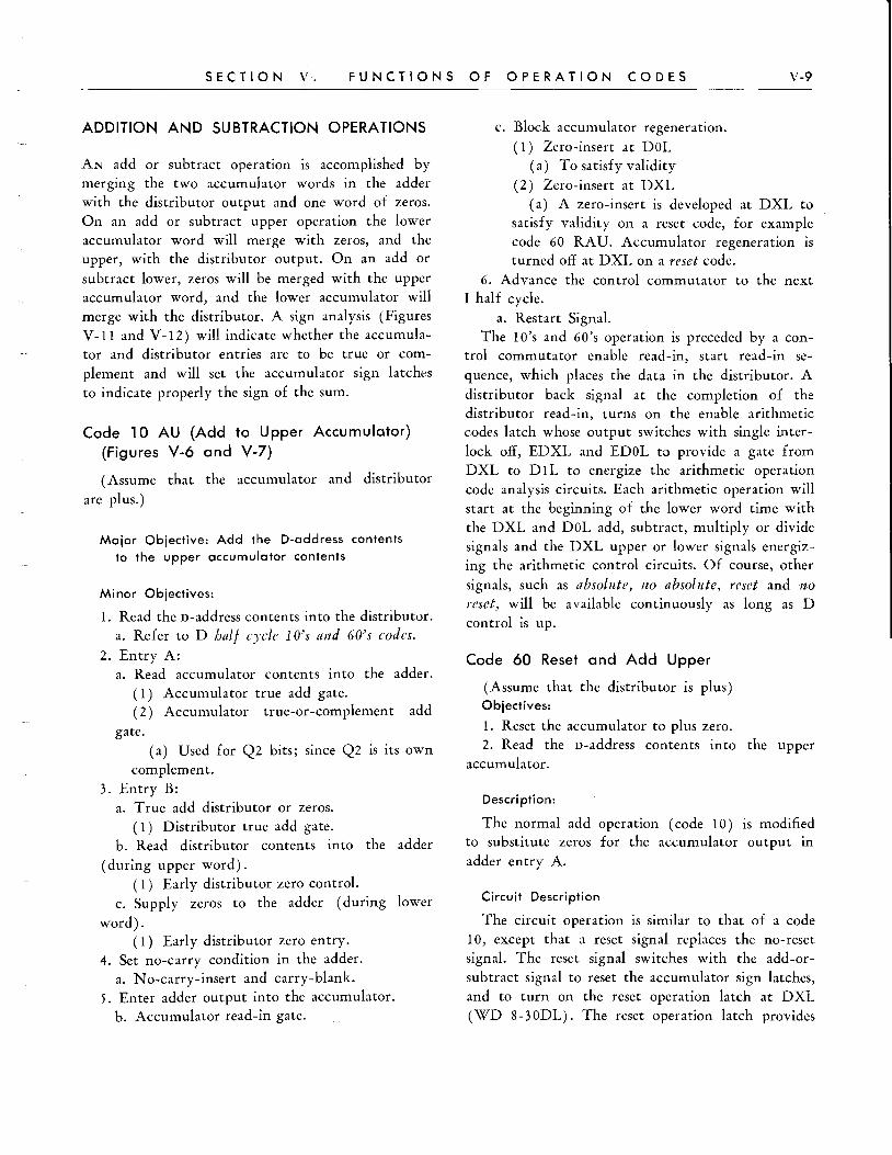
SEC T ION V. FUNCTIONS OF OPERATION CODES V-9
ADDITION AND SUBTRACTION OPERATIONS
AN add or subtract operation is accomplished by merging the two accumulator words in the adder with the distributor output and one word of zeros. On an add or subtract upper operation the lower accumulator word will merge with zeros, and the upper, with the distributor output. On an add or
subtract lower, zeros will be merged with the upper accumulator word, and the lower accumulator will merge with the distributor. A sign analysis (Figures V-II and V-I2) will indicate whether the accumulator and distributor entries are to be true or complement and will set the accumulator sign latches to indicate properly the sign of the sum.
Code 10 AU (Add to Upper Accumulator) (Figures V-6 and V-7)
(Assume that the accumulator and distributor
are plus.)
Major Objective: Add the D-address contents to the upper accumulator contents
Minor Objectives:
1. Read the D-address contents into the distributor. a. Refer to D balf cycle 10's and 60's codes.
2. Entry A: a. Read accumulator contents into the adder.
( 1) Accumulator true add gate. (2) Accumulator true-or-complement add
gate. ( a ) Used for Q2 bits; since Q2 is its own
complement. 3. Entry B:
a. True add distributor or zeros. (I) Distributor true add gate.
b. Read distributor contents into the adder
(during upper word). ( 1) Early distributor zero control.
c. Supply zeros to the adder (during lower
word). (1) Early distributor zero entry.
4. Set no-carry condition in the adder. a. No-carry-insert and carry-blank.
5. Enter adder output into the accumulator. b. Accumulator read-in gate.
c. Block accumulator regeneration.
(I) Zero-insert at DOL (a) To satisfy validity
(2) Zero-insert at DXL (a) A zero-insert is developed at DXL to
satisfy validity on a reset code, for example code 60 RAU. Accumulator regeneration is turned off at DXL on a reset code.
6. Advance the control commutator to the next I half cycle.
a. Restart Signal. The IO's and 60's operation is preceded by a con
trol commutator enable read-in, start read-in se
quence, which places the data in the distributor. A
distributor back signal at the completion of the distributor read-in, turns on the enable arithmetic codes latch whose output switches with single inter
lock off, EDXL and EDOL to provide a gate from DXL to DIL to energize the arithmetic operation code analysis circuits. Each arithmetic operation will start at the beginning of the lower word time with the DXL and DOL add, subtract, multiply or divide signals and the DXL upper or lower signals energizing the arithmetic control circuits. Of course, other
signals, such as absolute, 110 absolute, reset and 110
reset, will be available continuously as long as D control is up.
Code 60 Reset and Add Upper
(Assume that the distributor is plus) Objectives:
1. Reset the accumulator to plus zero. 2. Read the D-address contents into the upper
accumulator.
Description:
The normal add operation (code 10) is modified to substitute zeros for the accumulator output in adder entry A.
Circuit Description
The circuit operation is similar to that of a code 10, except that a reset signal replaces the no-reset signal. The reset signal switches with the add-orsubtract signal to reset the accumulator sign latches, and to turn on the reset operation latch at DXL (WD 8-30DL). The reset operation latch provides

CODE 10 OPERATION DIST. PLUS ACC. PLUS
CONDITIONS FOR ADDER CARRY CIRCUITS
SIGNALS FROM OP CODE AND "D" CONTROL
Enable Arilh. Code Lalch (7 - 10Bl)
HC Add 5 Off
He Add 5 Off
OP BOT OP QO
Q4 Q1UN
EDIL
To turn Single Intl'k On
OR .:t Add or Subt. Sig. l EDXl or EDOL
Adder Zero In,ert (S·- 30EU)
Carry Blank (S-30EU)
Single Inll 'k Off
Dist. Plus
Ace. Plus
EDO
No Carry Insert (S-30EU)
No Reset Sig. (7-2ICU)
No Absolute Signal (7-2ICU)
Wl(EV) W.L. (EV.W)
DIO-OR-DX DX-OR-DiO
• .LDbl. l lnv •
tlnv. t Early Dist. Zero Entry
Early Di,t. Zero Control
Dist. True Add Gale (Conditions Adder
r-----r----------------OR
Entry nsn Circuits)
I
OR
t Ace. True or Ace. True Compl. Add Add Gate Gate
(Conditions Adder Entry "A II Circuits)
Ace. True or Compl. Add (S-30Dl)
Ace. Read In Gale (8-30 CU)
Ace. Regen latch (8·3OCU)
WPL
Permits Ace. to accept Adder Input
NEDX
Blocks Ace. Regen
Figure V-7. Add Upper Function Chart--Code 10
V-10
Arith Op. Latch (S-30 DU)
by Ace. True or Campi. Add
Operation Interlock latch (7-lOCL) on with + Shift From 5T5
Restart ta Lag. (7-10)
D6
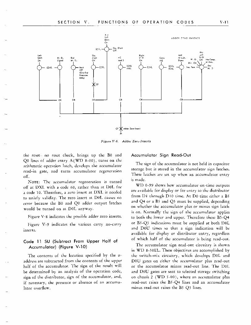
SECTION V. FUNCTIONS OF OPERATION CODES V-ll
left Shift On
EDXl
M. D. Signal
'----- OR
End M. D.
OR
Mult Off (Overlap Produces DXl)
EDll
Sig. Digit On
OR
EDOl
Aoy Left Shifl 00
Sig. Digit Off
He Add 5
OR
EDXl EDOl
Right Shift On
EDXL
Comp Adj
OR ___ ---l
ADDER ZERO INSERTS
EDXl EDOl
Acid or Subt. Signal
OR----.J
CF Adder Zero Ins-ert
Figure V-So Adder Zero Inserts
the reset-no reset check, brings up the BO and QO lines of adder entry A(WD 8-00), turns on the arithmetic operation latch, develops the accumulator read-in gate, and turns accumulator regeneration off.
NOTE: The accumulator regeneration is turned off at DXL with a code 60, rather than at DOL for a code 10. Therefore, a zero insert at DXL is needed to satisfy validity. The zero insert at DOL causes no error because the BO and QO adder output latches
would be turned on at DOL anyway.
Figure V-8 indicates the possible adder zero inserts.
Figure V -9 indicates the various carry no-carry
inserts.
Code 11 SU (Subtract From Upper Half of Accumulator) (Figure V-10)
The contents of the location specified by the D
address are subtracted from the contents of the upper half of the accumulator. The sign of the result will be determined by an analysis of the operation code,
sign of the distributor, sign of the accumulator, and, if necessary, the presence or absence of an accumu
lator overflow.
Accumulator Sign Read-Out
The sign of the accumulator is not held in capacitor storage but is stored in the accumulator sign latches. These latches are set up when an accumulator entry is made.
WD 0-99 shows how accumulator on-time outputs are available for display or for entry to the distributor
from Dl through DIO time. At DO time either a B5 and Q4 or a B5 and Q3 must be supplied, depending on whether the accumulator plus or minus sign latch
is on. Normally the sign of the accumulator applies to both the lower and upper. Therefore these B5-Q4 or B 5 -Q3 indications must be supplied at both DoL and DOU times so that a sign indication will be available for display or distributor entry, regardless of which half of the accumulator is being read-out.
The accumulator sign read-out circuitry is shown in WD 8-30EL. These objectives are accomplished by the switch-mix circuitry, which develops DoL and DOU gates on either the accumulator plus read-out or the accumulator minus read-out line. The DOL and DOU gates arc sent to selected storage switching on chassis 2 (WD 5-00), where an accumulator plus read-out raises the B5 -Q4 lines and an accumulator minus read-out raises the B5 -Q3 lines.
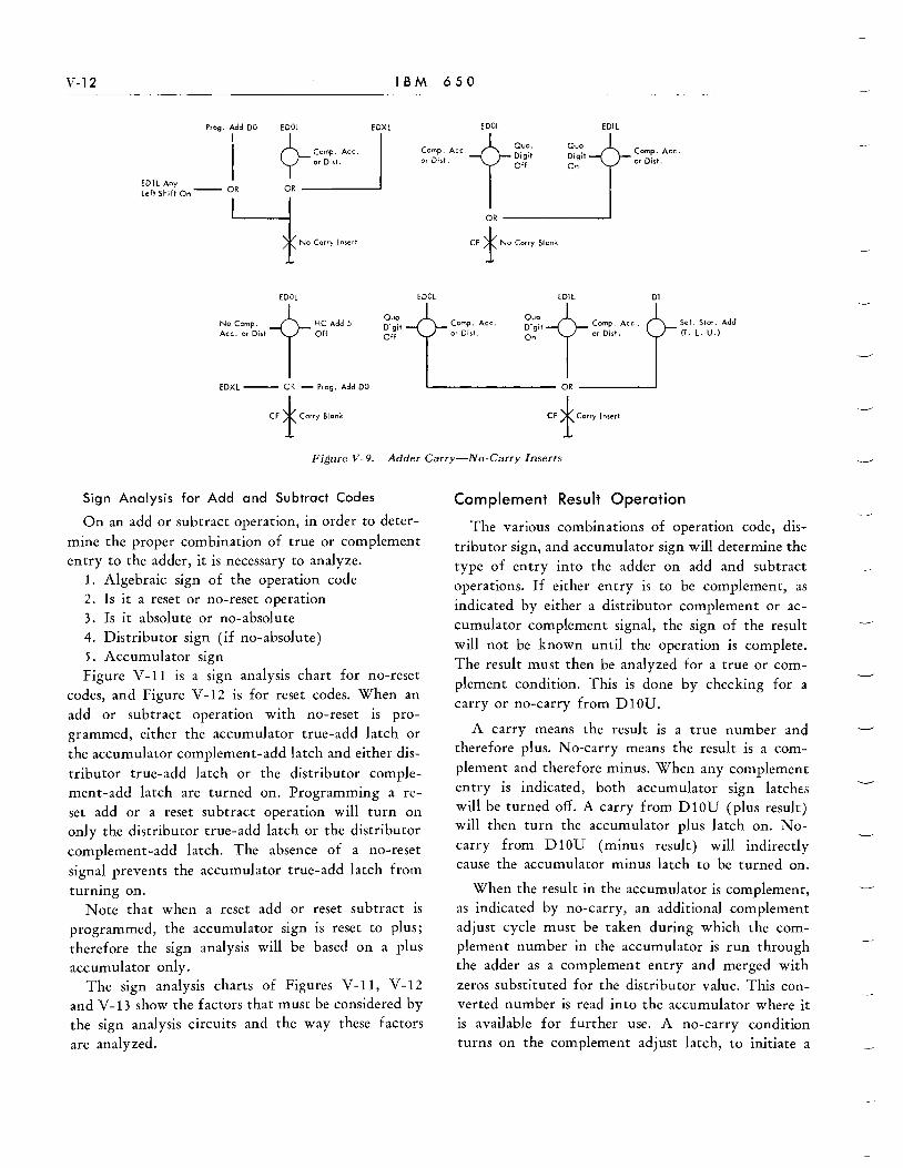
V-12 IBM 650
P,og. Add DO EDXL EDOL ED1L
Camp. ACC'~~i~~; .. ,,,' I 0"
Quo Digit On
Compo Ace. or Dist.
ED1L Any Left Shift On -- OR t N.~" ,,""
EDOL
No Camp. ~ HC Add 5 ", .' "" I 0"
Quo. Digit Off
EDOL
OR ------------~
CF f No Co"y Blank
Compo Ace. or Di$t.
ED1L Dl
~i~~t -6- Camp. Ace.
0, I .. ,,,,. Sel. Stor. Add (T. L. U.)
EDXL -- OR - P,og. Add DO OR _______ ----l
CF t Cm,y Blank CF t Co"y Inser.
Figure V -9. Adder Carry-No-Carry Inserts
Sign Analysis for Add and Subtract Codes Complement Result Operation
On an add or subtract operation, in order to determine the proper combination of true or complement entry to the adder, it is necessary to analyze.
1. Algebraic sign of the operation code 2. Is it a reset or no-reset operation 3. Is it absolute or no-absolute 4. Distributor sign (if no-absolute) 5. Accumulator sign Figure V-ll is a sign analysis chart for no-reset
codes, and Figure V -12 is for reset codes. When an add or subtract operation with no-reset is programmed, either the accumulator true-add latch or the accumulator complement-add latch and either dis
tributor true-add latch or the distributor complement-add latch are turned on. Programming a reset add or a reset subtract operation will turn on only the distributor true-add latch or the distributor complement-add latch. The absence of a no-reset signal prevents the accumulator true-add latch from
turning on. Note that when a reset add or reset subtract is
programmed, the accumulator sign is reset to plus; therefore the sign analysis will be based on a plus accumulator only.
The sign analysis charts of Figures V -11, V -12 and V -13 show the factors that must be considered by the sign analysis circuits and the way these factors
are analyzed.
The various combinations of operation code, dis
tributor sign, and accumulator sign will determine the type of entry into the adder on add and subtract operations. If either entry is to be complement, as indicated by either a distributor complement or accumulator complement signal, the sign of the result will not be known until the operation is complete. The result must then be analyzed for a true or complement condition. This is done by checking for a carry or no-carry from DIOU.
A carry means the result is a true number and therefore plus. No-carry means the result is a com
plement and therefore minus. When any complement entry is indicated, both accumulator sign latches will be turned off. A carry from D IOU (pi us result) will then turn the accumulator plus latch on. No
carry from DI0U (minus result) will indirectly cause the accumulator minus latch to be turned on.
When the result in the accumulator is complement, as indicated by no-carry, an additional complement adjust cycle must be taken during which the complement number in the accumulator is run through the adder as a complement entry and merged with
zeros substituted for the distributor value. This converted number is read into the accumulator where it is available for further use. A no-carry condition turns on the complement adjust latch, to initiate a

Provides Circuits
For Conditioning
Adder Entry A
And Accumulator (See Fig. V-7 for a
Code 10 Operation)
OR
Acc. True or Campi Add
No Reset
Carry
Insert
Quo. Digit OFF
Subtract Operation and Complement Adjust
Code II Acc Plus and Dist Plus
Ace. True Add Latch (8-30 CL)
No Absolute
Reset No Reset
Check
Campi.
Dist. Plus
Acc. Plus
Acc. Compl_ OR
Add Latch C I amp Acc.
or Dist
Adj. Off
NWPL Quo. Digit Off
Acc Carry Insert Mult - Sign And No Div Reset Carry Blank Off Dl0U (8-30 EL) (8-30 EU)
NEAP
Compl Result Test
Carry No Carry Test Test
ACC PLUS Compl. SIGN LATCH Adj. Latch
(8-30 EL) (8-30 DL)
Acc. Campi Add Turn On Latch Acc Minus EDXL
or Latch (8-30 EL) EDOL
Zero Insert (8-30 EU)
NWPL NWPl
Figure V-10. Subtract and Complement Adjust
V-13
Dist. Compl.
Add latch (8-30 Cl)
Dis!. Campi
Add Gate
NWPL
Add Zero
NEDXL
(8-31 AL)
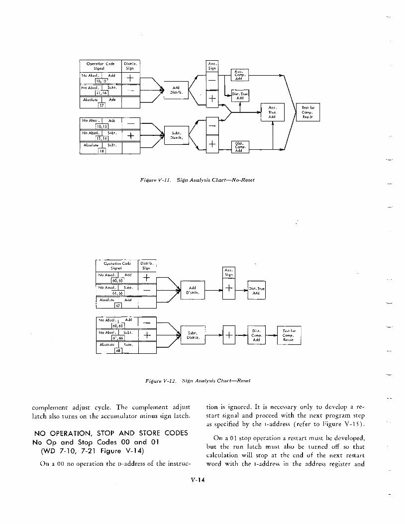
Operation Code Distrib. Signal Sign
+
+
Figure V-U. Sign Analysis Charl-No-Reset
Operation Code Signal
Distrib. Sign
+ Ace. Sign
Figure V -12. Sign Analysis Chart-Reset
complement adjust cycle. The complement adjust latch also turns on the accumulator minus sign latch.
NO OPERATION, STOP AND STORE CODES No Op and Stop Codes 00 and 01
(WD 7-10, 7-21 Figure V-14)
On a 00 no operation the D-address of the instruc-
V-14
tion is ignored. It is necessary only to develop a restart signal and proceed with the next program step as specified by the I -address (refer to Figure V -1 5) .
On a 01 stop operation a restart must be developed, but the run latch must also be turned off so that calculation will stop at the end of the next restart word with the I-address in the address register and

SECTION V. FUNCTIONS OF OPERATION CODES V-15
OP QOUN or Q2UN
Enable Arith. Codes Signal
OP QIUN or Q3UN
OR OR------------~
Ace. Camp Add
Latch
Dist True Add
Lotch
EOO No Reset Signal
OR -----------"-' t Ace True Add
latch
OR i D;;' Compo Add
Latch
SIGN ANALYSIS FOR ADD AND SUBTRACT
Code, 10, II, 15, 16, 17, 18,60,61,65,66,67,68
Figure V -13. Sign Analysis for Add and Subtract: Function Chart
the control commutator ready to continue on the interrupted I half cycle (refer to Figure V-16).
Major Objective: Stop the control commutator just before I con
trol of the next I half cycle.
Minor Objectives:
1. Advance the control commutator into the I
half cycle. a. Restart signal
2. Block I control
a. Turn off run latch
Sensing an Olin the operation register with D
control on turns off the run latch if the programmedstop switch is set to STOP. At the same time, the restart signal is developed to advance the control commutator through restart B time of the next I half cycle.
If the programmed-stop switch is set to RUN, an 01
code is treated as a no operation code.

,
Assume that the 650 i~ operating with the rollowing series of program deps' 'Xx kX". 0013 00 0000 0017
0()()9
Re,tort ~
0010 0011 0012 0013 0014 -~OOl5 =f-'OOl6 00/7 --I--- ----
. I - Note: Oevelopment or '"0" Restort A Restort A
control with a 00 OP code gi ves 0
restart signal
Re,tart B Restart B Re~tort B
Enable Reod-In Enable RI AOOR OP AOOR AOOR
~ , ~ I ooool~ Stmt RI Start RI
RIPS RIPS
(RI 00 0000 0017) RI fro", 0017
n One Word Eorly n "I" A'ternation [I r
"I" Control II
"Oil Alternation II II
"0" Control n I
If the 650 i, operating with the follow
then the operat;~ is changed
ing senes 0 program steps, xx )(.xxx 0013 010000 0017
as shown here ------+--estort A Restort A
Restort B Restart B
~ AJOR AOtR OP
01 I 0000 I ~
\..-n II "I" Alternation
r--- I "I" Control
"0..1 Alternation (--,I [I
J n "0" Control
I Run Control
FiRure V-14. Control Commutator Operation-Code 00 /lJ> 01
V·16
~
IL.-t
Iy
,

AP
"I" OP Light
DlD5
R.I. Add,. Reg.
NWP
"D" Control
Reset Op. and Addr. Register's
Restart A
Run Control
Read - In Prog. Step (RIPS) Refer to Figure
V-2
DID5
R.1. Addr.
Reg.
CF
Restart S (7- IOAU)
NWP
Restart [}
"D" Control
Rese~ Op_ and Add!-. Reg,sters
CF (7-21Bl)
"I" Control (7 - JOAU)
Prog. SlOp 5w. Set to STOP
Run latch (7 - IOAl)
Figure V -15. No Operation--Code 00 Figure V-16. Stop Code-Code OJ
0001 0002
I R."o,'A C
Restart B
AJOR 10005 I
CONTROL COMMUTATOR OPERATION, 20Code STL
Anume that the 650 i\ operating with Ihi\ \efic\ of program iteps: )(x xxxx 0005 200011 xxx x ....
0003 0004 0005 0006 0007 01308 0009
upper lower
Restart A
Restart B AfirUtm.p:o
AJOR DIOU (RIO:,. 012
13456789)
D9 DP
Enable RI ~ Enable RI
~tart RI tJ 0 RIPS
RI 200011 xux
I One word early
I [1 'I' Alternation
II 'I co:L
II "0" Alternation
"0" Control
I Figure V-17. Control Commutator Operation-Cod", 20
V-ll
0123456789 in upper accumulator
0010 0011
Re~tort A ~~
D9
Start RI b 010 0 RIGS
Store 0123456789 in 0011
n Ir
~ i"--

V-1S IBM 650
o Control
CF Stort Ace. 10
Dis .. R.I.(7-10SL)
Enable Read- In (7 - WSU)
Di~t. Di~t. Regen. Back Control Signal (6-1OCU)
D9
All Restart
Di~t. Regen. Control
Singla Intlk.
Figure V -18. Store Lower Accumulator-Code 20
Store Codes (20's) (WD 7-10, 7-21)
Objectives:
The store codes provide a means of transferring
information from arithmetic storage in the accumu
lator or distributor to general storage. A store opera
tion code is always accompanied by a general storage
D-address. The store operations have the common
characteristic that the number stored is also in the
distributor after completion of the operation. The
number contained in a memory location is automatically erased as new information is read into it. The contents of the accumulator is not affected by this operation. The D-address specifies the location in
which the number is to be stored. The next instruction is taken from the location specified by the J
address. A brief description of the store codes follows:
ST L Store LGluer Half of Accllmulator (20).
Major Objective (Figures V-17 and V-1S):
The contents of the lower half of the accumulator
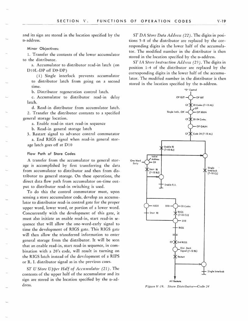
SECTION V. FUNCTIONS OF OPERATION CODES V-19
and its sign are stored in the location specified by the D-address.
Minor Objectives:
1. Transfer the contents of the lower accumulator to the distributor.
a. Accumulator to distributor read-in latch (on
DI0L-DP off D9-DP) (1) Single interlock prevents accumulator
to distributor latch from going on a second time. b. Distributor regeneration control latch. c. Accumulator to distributor read-in delay
latch.
d. Read-in distributor from accumulator latch. 2. Transfer the distributor contents to a specified
general storage location. a. Enable read-in start read-in sequence b. Read-in general storage latch
3. Restart signal to advance control commutator a. End RIGS signal when read-in general stor
age latch goes off at DI0
Flow Path of Store Codes
A transfer from the accumulator to general storage is accomplished by first transferring the dara from accumulator to distributor and then from distributor to general storage. On these operations, the direct data flow path from accumulator on-time output to distributor read-in switching is used.
To do this the control commutator must, upon
sensing a store accumulator code, develop an accumu·· lator to distributor read-in control gate for the proper upper word, lower word, or portion of a lower word.
Concurrently with the development of this gate, it must also initiate an enable read-in, start read-in se
quence that will allow the one-word-early signal to time the development of RIGS gate. This RIGS gate will then allow the tr'ansferred information to enter
general storage from the distributor. It will be seen that an enable read-in, start read-in sequence, in com
bination with a 20's code, will result in turning on
the RIGS latch instead of the development of a RIPS or R. 1. distributor signal as in the previous cases.
ST U Store Upper Half of Accumulator (21). The contents of the upper half of the accumulator and its sign are stored in the location specified by the D-ad
dress.
ST DA Store Data Address (22). The digits in positions 5-8 of the distributor are replaced by the corresponding digits in the lower half of the accumula
tor. The modified number in the distributor is then stored in the location specified by the D-address.
ST fA Store Instruction Address (23). The digits in position 1-4 of the distributor are replaced by the
corresponding digits in the lower half of the accumu
lator. The modified number in the distributor is then stored in the location specified by the D-address.
One Word Ea dy
NEDI
Start RI
OP Q2T
S;ngle In.lk. Off
Enable RI (7-10 BU)
Enable R.I.
"0" Coo"ol
D10 20 Codes
Single Interlock (7-10 Cl)
Single Interlodc
Figure V-J9. Store Distributor-Code 24
V-20 IBM 650 --------------. ------------
ST D Store Distributor (24) (Figure V-19). The contents of the distributor are stored in the location specified by the D-address.
If a store distributor code (24) is sensed, the accumulator to distributor control is not developed. Instead the enable read-in, start read-in sequence is started. This results in the development of a RIGS gate and the entry into general storage of the data already in the distributor.
SHIFT CODES (30, 31, 35 and 36)
THE FOUR SHIFT operations, shift right (Code 30), shift right and half correct (Code 31), shift left (Code 3 5 ), and shift left and count (Code 36) are all performed by repositioning the digits stored in the accumulator. No transfer of data between storage locations is required. The program control circuits sense the shift code and send a properly timed signal indicative of the shift operation to the arithmetic controls. Restart from a shift operation is similar to an arithmetic operation, and operation interlock is required because the performance of a shift operation may require several word times.
When the shift code is 30 or 35 the program controIs must also determine whether or not the shift number (units position of address register) is zero. If it is zero, no signal is sent to arithmetic controls and a restart is developed.
Proper timing of the shift signals is accomplished by the shift control latch. It must be remembered that the D control signal, developed when restart B goes off, starts at the beginning of a word interval, but the word could be either upper or lower. All shift operations start at lower word time. The shift control signal is timed to occur just prior to the beginning of a lower word and insures that the signals will be developed during a lower word interval.
The units digits of the D-address of any shift instruction specifies the number of shift cycles. The calculator will shift the contents of the entire accumulator only by the amount indicated by the units
digit. The next instruction is taken from the location
specified by the I-address. The contents of the distributor are not affected by these operations. Any digits shifted off are lost, and no indication is given jf this should occur.
Code 30 SRT (Shift Right) (Figures V-20, V-21 and V-22)
Major Objective:
The contents of the accumulator are shifted to the right the number of places specified by the units digit of the D-address. A zero indicates a shift of no positions, a one indicates a shift of one position, etc.
Minor Objectives:
1. Enter the ten's complement of the shift number (the units position of the address register) into the accumulator (DOL position).
a. Shift number gate at DXL, on first shift cycle only.
b. No-carry at DXL. c. Special digit add 1 at DXL. d. Accumulator read-in at DXL.
2. Supply zeros to accumulator. a. Zero insert at DXL.
3. Shift each position of the accumulator, except DOL, one position to the right.
a. Right shift gate (DIL-DXL). b. Turn off accumulator regen. latch.
4. Advance the shift number by one. a. Accumulator true add at DXL. b. No carry at DXL. c. Special digit add 1 at DXL d. Accumulator read-in at DXL
5. Stop shifting. a. DOL carry. b. Turn on accumulator regen. latch. c. Turn off operation interlock.
Right shifting is accomplished by allowing each accumulator early-digit output to control the pedestal lines. Thus D2L is read out at DIL time, controls the pedestals and reads back into the DIL position at DIL time. Each digit successively follows this procedure for the two accumulator word times, with the result that the accumulator number is shifted one position to the right. The number of shifts taken is controlled by the value of the units position of the D-address (in the address register), which accompanies the shift operation code. Each shift requires two word times, and in the following descriptions each of these twoword intervals is called a shift cycle.
On the first cycle of each shift operation the units position of the address register enters the adder at
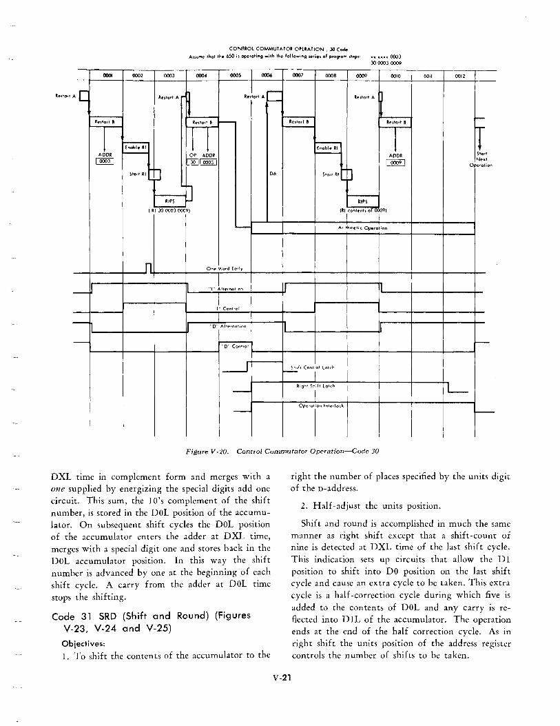
CONTROL COMMUTATOR OPERATION, JO Code Assume tha' the 650 it operating with the following sefiet of program dept· Xl( IO(JlX OOCIJ
JO 0003 0009
0001 0002 0003 0004 OOOS 0006 0007 0008 0009 0010 0011 0012
AC ~
I~ ~ Retlo" A Rettar' A Restart A
""'-
l -.~Ito't B Re~to,t B - Rellert B Retlar' B
.L ~1 .L I Enobl. II fnoble RI
I 0003 I LQOO:::iJ Next Operation
Slort RI J 06 Starl RI Q
liPS ]
RIP5
( R r 30 0003 0009) (RI I contenh of i -9)
""'- Arithmetic Ope-rolion
n One Wo,d Early
I n "'" AItNnolion II -I
"'" Control
-II ,
II "0' Alt(,rnol;on II
- -"0" (oMrol
---.J Shifl Control lotcr. r--
I RIghi Sh;/t latch
-----' I Operation Interlock -----
I -
Figure V-20, Control Commutator Operation-Code 30
DXL time III complement form and merges with a one supplied by energizing the special digits add one circuit. This sum, the 10's complement of the shift number, is stored in the DoL position of the accumu-lator. On subsequent shift cycles the DOL position of the accumulator enters the adder at DXL time, merges with a special digit one and stores back in the DOL accumulator position. In this way the shift number is advanced by one at the beginning of each shift cycle. A carry from the adder at DOL time
stops the shifting.
Code 31 SRD (Shift and Round) (Figures V-23, V-24 and V-25)
Objectives:
1. To shift the contents of the accumulator to the
V-21
right the number of places specified by the units digit of the D-address.
2. Half-adjust the units position.
Shift and round is accomplished in much the same manner as right shift except that a shift-count of nine is detected at DXL time of the last shift cycle. This indication sets up circuits that allow the D1 position to shift into Do position on the last shift cycle and cause an extra cycle to be taken. This extra cycle is a half-correction cycle during which five is added to the contents of DOL and any carry is reflected into DIL of the accumulator. The operation ends at the end of the half correction cycle. As in right shift the units position of the address register controls the number of shifts to be taken.

......
N tV
~I ~ u u ~ ~rl------------------~ ~~------~ 5 (0' Oil 2nd Cycle 5 (a D2l 1st Cycle
o o ~
~ .R ~ o @
Add I to 9 (a DXl time to get a DOL Carry from Adder
Thh causes RS late" to go off.
>-]
~ i~
Accumulator Read-In
Gate
1' ....... '- "-'AL Right Shift Gate
______ -+ _________________ -:-______________ --'~Shift Number Gate
I I
f"'i5"Xl'i roxn Accumulator True Add Gate ----~ I
~ 'DOL >Dxq 'DOL DXlL-- Accumulator Read-In Gate
I I r--- Accumulator Regenecation --, I !
,-----2nd Right Shift Cycle +- ---- I,t Right Shift Cycle-------1 < TIME
Figure V-21. Shift Right: Block Diagram-Code 30
DOL 1,1 RS Cycle
9 :,c, Do;. 2nd RS Cycle
I
• DXL Early [ = t ~'1-=-7(2DXl T -I · I Special Digit DXl
I,t Cycle Only
No C<my I ",ort (NCil , DXl
every cycle
Shift No. Gate DXl 15t Cycle Only
Anume a 650 Operation Code of 30 0002 XXXX Assume that a 5 in 03l is being shifted to ott.

o Control Single Interlock OFF
Inv. and CF
Neg. Sh ift Num Gate (8-30 DU)
Blocks Ace. True Add Gate during first cycle.
DIOU
EOXU
t" Turn Single Intlk ON
l.S. -OR-Half Correct
CF f 5hat Numbe, Gate (8-30 AU)
To enter camp. of un its p05. of
Add" Reg, into Add", Entry A (DXL)
MULT, DIY LT - 5H -OR- LT. 5H,
DXL
Add One To Add", Entry 8
Ac c. T rue Add Gate to Enter Ace. Early Output (DOL Count of Num. of Sh ;Its) into Adder Entry A.
(for each shift cycle except the first)
Note: No Carry Insert every EDXL. No Corry Insert with no Compo Ace. or Dist. and H,C. add 5 OFF.
Ace. Regen (8-30 CU)
CF Any Shift
(8-30 DU)
Turn ON Arith. Ope,ation (8-30 DU)
(Arith Restart)
WL
OR------l
No zero 5h ift number
EDXL
SOUn Code 31 -OR- Code 36
OR- Half Correct ~jgnol
Right 5h ift Latch (8-30 AU)
EDXL EDXL 0,
EDOL
Zero Insert
To Adder Output
INO ze'o ,hilt Num, on 30 or 35 Codes
Operation Intlk
(7-10 CL)
Neg. EDXL
0' EDOL
Gate (8-30 AU)
Allows Ace. Early
Ovtput to Control
Aec Pedestal
t:::R3S5 Caery
OX
Neg, (Shift Count 51g, o,H,c'S I9)
CF
H ,c, Add 5 -OR- Man Acc, Re.et
AlloW! Arlth. Op, Latch to turn OFF at EDX. This develops a end - of -operation slgnol to turn OFF Operation Intlk.
WPL
DOL Carry Latch
Figure V -22. Shift Right.' Function Chart-Code 30
\' -23

--: , IV .j:>.
0 -c >-u
i ~
. 1 u
~
~ ~
9@ OIL HaH Correct Cycle
e @ DOL lit Cycle
Note: Adder Output "9" C0U191 O?ertltio .... of the Right Skift Gate at DOt time inltQod 0' at OIL and 0110 tums on tne Half COrTe.;t Add 5 latch. !I
@ ! 1 l'HI'"" ~ o .':- E Note; w,?" (a, DOl of 2nd cycle
con not get through switch since Ace RI Gate is down.
Note: Adder OutPl,lt of I~ DOL of H.C.Cyclt' It blockGd by DOL Olnulf1. T},e Ccrty L.etch i. tet 10 thot ""I-Ien the 8 in 01 L i. odQK to a Spec;;iol O:git 0, In" Adder Ovtpvt is 9@ Oil timli!.
9 @ DOL 2nd RS Cycle
I I I
Blodc-Itd ot COL, open 01 Oil
51 51 wr ! ! >I l!. Q U
(D :l:
: I I
l Eor y He Correct eye e - , - -: - -tNcI' 8@ DOL Early Half Correct Cycle __ I _ ~ _ LD~t_
8 t?...) DXl (lIOf"ly) Cycle tNCI I !.:'Xl
7@;.OXl - -I DOL - - - -lit Cycle OnIY,I-_:-_+-__ _
J """ .. !
No Corry InMrt (NCt) OXl, DOL
Shift No Gato DXL 1st Cycle Only
orr DOL I ADDRESS 1)1:"",("
I ! DXl L... Hal f Correcl latch -....:...---------- I I
~ : DOL' I Half Correct Add 5 latch
S SpQciol Dig;'@ OXl of H.C. eyel. o Special Digit exc~pt Qt OXL
or H.C, Cyelt;'
I Spli!cioi Digit DXL evety'RS cycfe
~ I
~----------~D::::O:"1l ~ ! DOL DXll Right ,hilt Got.
Auume a 650 Operation Code of 31 0002 XXX)( Anumi(' thot 860 is in DIL.D2l. and 03\.
--~-----------~ I I
I rDXl"1.-. Sh i ft No Gote i I I
-iD1(XJ DXl' fDxl'IL ______________ -:-__ Ac.cumulator True Add G<lff:
I I I
----l DX'! ~ ~Accumula""Reod-IO Got.
I I Accumulator Regen~rat.oo --,~------------~----------~------------~ I
I-----Holf Adl~t (yel. -----t---- 2nd Ri~t Shift Cycle ht Right Shift Cyci(: --\
<:: TIM£
Figure V-23. Shift Right and Round: Block Diagra~Code 31
(

o Control
No Zero Shift number Inv.
& CF Neg. Sh 1ft Number Gate
DXl
Ace. True Add Gat.
EOOl
)( I CF
OPQOUN EDXl Shift Control
Turn Singl. Intlk ON r-----------------~r_------------~~~==~-------------------+------~OR
Holf Correct latch (8-30 AU)
Neg (Sh. CT. '" H.C.) (8-30AU)
Operation
alocks OOL Carry on First Shift cyle. l.S.-OR-R.S. OR
l CF Intlk (7-10Cl)
EDXl - No Corry Insert EOOl - No carry Insert When HC Add 5 i. OFF ond there is no Comp. ACC, nor Dist.
EOXL
Significant digit OFF
Ace. R.I.
for H.C.
CF *- Shift Number . ~ . Gate (8-30 AU)
To enter compo of units pos. of Addr. Reg. into Adder Entry A (DXL).
EOXl
MUlT. OIY _ OR _ IT SH LT. - SH. • •
ANY SHIFT (8-300U)
Turn ON Arith.OP
Ace. Regen. (8-30 CU)
Adder Enty a Adder Entry A (as & Q3)
Half Correct Add 5 latch (8-30 AU)
Add "5" Add "0" Zero Insert
Neg (EDXlor EOOL.)
Right Shift Gate (8-30 AU)
Allow. Ace. Early output to control Ace. Pedestal.
Right Sh ift Gate (Tran •. Dll to OOL for H. C. cycle only)
H.C. Add 5 Ace. Regen ON
Figure V-24. Shift Right and Round: Function Chart-Code 31
V-25
Right Shift latch (8-30 AU)
CF
Zero Ins:ert
EOXL
EDXl
or H.C. Add 5 OFF EOOl
Ace. Reod- in Gat. for Right Shifting
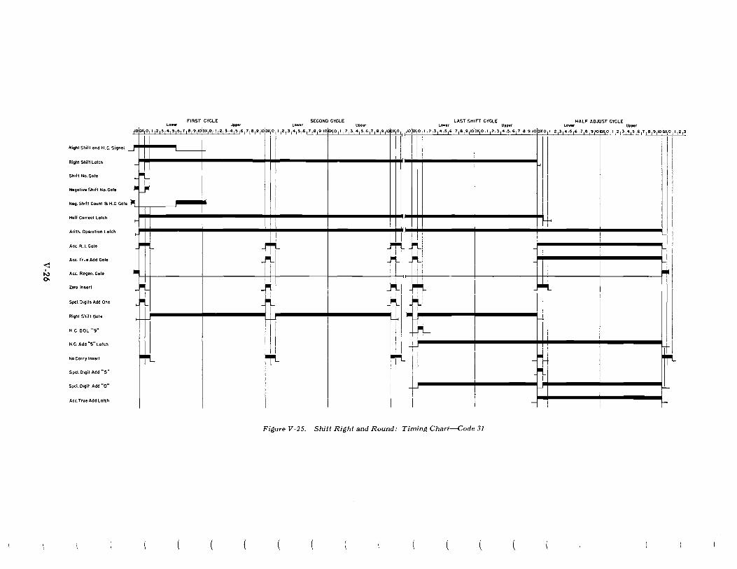
FIRST CYCLE SECOND CYCLE LAST SHIFT CYCLE Low., Upper
HALF ADJUST CYCLE Loww Upper Low" '- L ..... UP ..
012345678910 DXO 1 2345678910 012345678910 01234567891DO lolox.o I 2 3 4 5 6 7 8 9101mc.0 I 2 3 4""5 6 7 8 9 101D) 0 I 2 3 4 5 6 7 8 9 10~0 I 2 3 4 5 6 7 8 9 10 o I 2 3
RiQht Shift and H. C. SiQnal
Right Shift Latch f.<
Shift No. Gate
NeQative Shift NO-Gote
HeQ. Shift Count 8: H.C" Gate
HoJf Correct Lotch ....
Arith. Operation Latch
Ace. R. t. Gate
Ace:. True Add Gote ~ -~
~ ~ Acc. ReQen. Gat,
-po
0. Zero Insert ~ ~I-
Spcl. DiQits Add One H-I R;Ijh' StU" Ga'. H.C. DOL "9"
-I-' I ~
H.C. Add "s" Latch
No Carry Insert
!-'
~ i -l-Spcl. OiQit Add II 5 11 I-
I Spcl. DiQit Add "OH t-' f--' '-
Acc. True Add Latch I - t--
Figure V-2S. Shift Right and Round: Timing Chart-Code 31
( ( (

;1 '" ......
8J -'Io! ~~
t ;1 i ~ .!;
0
... l .3 il X 0
@, 0-
Add I to 9@ DXL lime to gel DOL Carry from Adder
I Th i s couteS LS Lotch to go off.
I I
o .. 5~~ @Iv 0. .q
] -' )( 0 @J
-'
t ! ~I c
E g
;:; @,
t
1 0
-',-8~ @J~ co-"
a; ~
Accumulator Read-In
Gote
8 @ DOLI" Cycle 1st Cycle
I
I I
I ..
I I 8@ OXl Early --l -L t:-
-- I NCI 5 @ Oil 1st Cycle I _ L _ _ 14--+- 0 Special Digit excepl (9; OXl
5 @ D2l 2nd Cycle ~CI I _ I Special Digil @ DXl every cycle 17@DXL •
1st Cycle Only No Corry I nX'rt
(NCI) DXL
Sh;l. No. Go •• @' DXL I,. Cycle only.
Register f __ . I ~~ ~~~~
_____ ....JIDIOU I!:!I IDOL DXl! ~ IDOL DXl: Lell Shill Gal.
I r=-I I IDXL L- Shift Number Gal. I
rDxil roxLi ____ oJ. 1 ' U,",L '~ ______________ ..J. __ Accumulator True Add Gote
~bOl -~ ~ Accumulator Read-In Gote
r Accumvlator Regeneration
ImlL ____ ~ __ ----__ --------~----------------~. I--- 2nd Left Shih Cycle-----'- lit Left Shift Cycle---...,
ASlvme a 6.50 Operation Code of 35 0002 XXXX Aslvme thot 0 5 in Oil i$ being shifted to 031
~===:;;::::::::=:= Figure V-26. Shift Left: Block Diagram-Code 35

DIOU
Inv & CF
Neg. Shift Num. Gote (8-30 DU) (Blocks Ace. True Add Gate during first cycle)
Turn Single Intlk On
Half Correct - OR - Right Shift
DXl
EDXl Sig. Digit Off
f Shift Number Gate (8-30 AU)
To enter campi. of units pos. of Addr. Reg. into Adder Entry A (DXl)
Any Shift
EDXl
(8-30 DU) Zero Insert Adder Ou tput
(8-30 EU)
Turn On Adth. Op.
OR- Add Sub
Ace. R.1. Gote (8-30 CU)
Ace. Regen (80-30 CU) Add One Adder Entry B
Ace. True Add Gate to enter Ace. Early Output (DOL Count of Num. of shifts) into Adder Entry A. For each shift cycle except the first.
Ace. Regen (On Dll)
~ Wl-Q-OI or 03
OR -WPL
OR
Inv.
CF
OR -Multl- Div, LT .SH.
Code 31 - OR - Code 36
CFl No zero ,hilt number on 30 or 35 cod ..
Operation I ntlk (7- 10Cl)
Neg (00, Significant ~=:;;'"4p-____ ...... _____ ...,o;git Oll)~
Adder Reset (8 - 10AU) Shilts the Adder Reset Gate one digit later.
Add Zero Adder Entry B
Zero In",r'
No Corry Insert (EDIL)
eOXL - No Carry Insert eDOl - No Carry Imert; H.C. Add 5 Off and
No Camp. Ace. nor Dist.
OR
t NDX
To odder Entry A. Allows Ace. On Time output to enter Adder
DOL Carry latch (8-30 BU)
EDll
Significant DlgltOIf
OR -~~:; Ace.
'NPl
Mise. Error Check (8-31) BL
Figure V-27. Shift Left: Function Chart-Code 35
V-28

SECTION V. FUNCTIONS OF OPERATION CODES V-29
A data address with a units of zero will result in
a right shift of ten with rounding. A carry from DOL will occur on the first shift cycle when the shift number is zero. Code 31 develops a negative half-correct signal to block this carry-stop.
On the last shift cycle the contents of the accumulator D IL position enters the DOL position via the
right shift path. The shift count number, coming from the adder output, is blocked. This is accomplished by the half-correct-add-five latch turning on at DOL, and blocking the accumulator read-in gate.
Removal of the OFF output of the half-correctadd-fi ve latch also prevents the no-carry insert at DoL time of the half-correct cycle. This allows the carry or no-carry status of the adder latches to be determined by the result of the half correction.
Code 35 SLT (Shift Left) (Figures V-26 and V-27)
Objective:
The contents of the accumulator are shifted to the left the number of places specified by the units digit
of the n-address. On a left shift operation the accumulator on-time
output enters the adder. It is merged with zeros from the B input and is available from the adder output one digit time later, to be stored in the accumulator
one digit position to the left of its original location. In this case the D 1 OL position of the accumulator is read out at D9L time but held in the early latches
during D9L time and is presented to the adder from
the on-time latches during D I OL time. For proper left shift operation, the D I OL in
formation must be available from the adder output
at DI U time, for storage in the DIU position of the accumulator. The DIOL information cannot be held
in the on-time latches because they are reset at DXaU time. Therefore, the DIOL information must
be transferred to the adder latches by normal adder
action at DXaU time and held there through DI U
time. The status of the adder latches must not be al
lowed to change until after DI U time, when their information is read into the accumulator. The DIU
position is read-out to the early latches at DIOL time as usual and stored there until transferred to
the on-time latches when the early latches are allowed to reset at DiaU time. This DI U information
is presented to the adder from the on-time latches during DIU time and the carry or no-carry indication from DIOL must still be available at this time
for proper analysis of the DI U information. This carry no-carry indication will still be available in the carry no-carry latches if they are not allowed to change until after DI U time.
To accomplish this, no new information must be
presented to the adder latches during DXU and DoU time and none of the adder latches must be reset
at DOaU or DiaU times. The left shift gate is closed at DX and DO time,
insuring that no new information will enter the A input during these times, thus blocking any new input to the adder latches. The adder reset control latch is controlled to block latch resets at DOaU and DIaD
times.
Code 36 SCT (Shift and Count) (Figures V-28, V-29, and V-29A, B)
Objectives:
1. The contents of the accumulator are shifted to the left until,
a. A no-zero is sensed in the D IOU position, or b. A DOL carry is sensed (except on the first
cycle) .
2. Enter the number of shifts in the DIL and D2L positions of the accumulator.
A left shift and count operation is accomplished
much the same as left shift except that the appearance
of a significant digit in the accumulator DIOU position is detected to stop the operation. The shift number in the address register units position is usually zero; so the shift count number in the accumulator DOL position indicates the number of shifts used before a significant digit is sensed in DIOU. If a
DOL carry is detected before a significant digit appears in DIOU, it is an indication that the maximum allowable number of shifts has been taken. The over
flow circuits will be set up, and a shift count of 10
will remain in the accumulator D2L and DIL positions.
When a shift number of zero accompanies this operation, the maximum allowable number of shifts
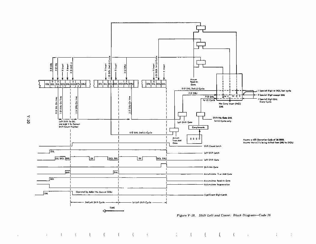
~ W 0
NI = o 0
@I @! o
i § ~ .£ .5 0
@I
~
u S
t ~I i l o ~
-------r-------------~+I----------------~--, S
::> i ... 0
0 @I
t
i T I
Aecum : Read-In I
I I
Gol. I I I
o @l DXL 2nd LS Cyel. _ ~ __ t _ + _ I Special Digil 01 DOL 1 .. , cyel.
2@OSU -~-~-N-cl- OSpeeioIOigil .. .,.,pIOXL
l r I ;:: I "<:
~ - .! <5 15
9@ DXL __ N _C _ _ _ _ I Speciol Digit DXL
ht lS Crcle Every Cycle c5 0 < I 0
~ 0 I ::> ... is 0 0 o
I @I @I ~ I
('" 0 - "
I ----Le" Shi', To DIL and Add 1 To Correct $hi h Count Number
I I
O@ DXl 2nd lS Cycle
I Aecum I True Add II Gole ___________ ~I L-_____ __
No eo.." I_, (NCI)
OXL
Shift No. Gate OXl
lsI LS Cyel. only
Shift Count Latch
-------.J D2l I I left Shill loleh I I I ~ ~ ~ ~ IDOL DXLJ left Shifl Gole
----- I I I
I I n Shift No Gol. I I
________ --'roxu [DXll Accumulator True Add Gate I I
I 02L I Accumulator Read-In Got. -------' I Accumulolor Regenerotion
I I
~ 061.. Operated by Adder No Zero at DIOU I Significant Digit lotch
I I
I, 2nd left Shift Cycle , " 1st left Shift Cycle _I
I TIME
<J~~=~
Anume 0 650 Operotion Code of 36 0000 Au""", lhol a 2 i, being ,hifled '- oaU to OIOU
Figure V-2S. Shift Left and Count: Block Diagram--Code 36
(

SECTION V. FUNCTIONS OF OPERATION CODES V-31
Inv. & Neg Shift Num. Gate (8-30 DU)
eF
eF Develop Ace. True Add Gate at DXLi each shift r cycle except the first, t
(See Shift left fvndion chart.)
)(
Turn Single Intlk ON
D Control Single !ntlk OFF
OP (BOT, Q3T)
Shift Control latch (7-21 aU)
EDXU
CP DIOU
Neg.SH.e!. (8-30 AU)
Blocks DOL Carry on firstshift (;ycle
EDll (8-30 BU)
cOO. DOL Carry Latch
ep Adder NO Zero
(See Sh iff left
function chort)
eF (8-10 AU)
r-------9R------~
Significant
Digit Latch (8-30 BU)
Stop Overflow Switch Sense eF (8_10 AU)
eo & QO Ace.
Ace. Regen.
OJ
Overflow Stop Latch (8-10 AU)
Overflow Sense latch (7-21 AI.)
PEO. Cf'o (6-00 EU)
Arith. OP. eK. (S-30 OU)
(8-31 Bl)
~----~OR~----~
Pklce zerO'$. in Oil & D2l
P::Isitions of the Accumulator.
t Overflow
light (7-02 A)
Run latch (7-10 A.)
Add "I" & Zero Insert
06
Figure V-29. Shift Left and Count: Function Chart--Code 36
is ten. If it is desired, for any reason, to limit the number of allowable shifts to fewer than ten, the number of allowable shifts desired can be indicated by the value of the units position of the D-address. In this way the number of shifts needed to cause a DOL carry is reduced. If, in this case, a significant digit is sensed before a DOL carry occurs, the shift count number in the DIL and D2L accumulator positions is the ten's complement of the unused allowable
shifts.
BRANCH OPERA nONS (40's and 90's Codes) Code 44 (Figure V-30)
BRNZU Branch on Non-Zero in Upper Half of
Accumulator (44)
The contents of the upper half of the accumulator are examined. If it is zero, the next instruction is taken from the location specified by the I-address. If it is not zero, the next instruction is taken from the location specified by the D-address.
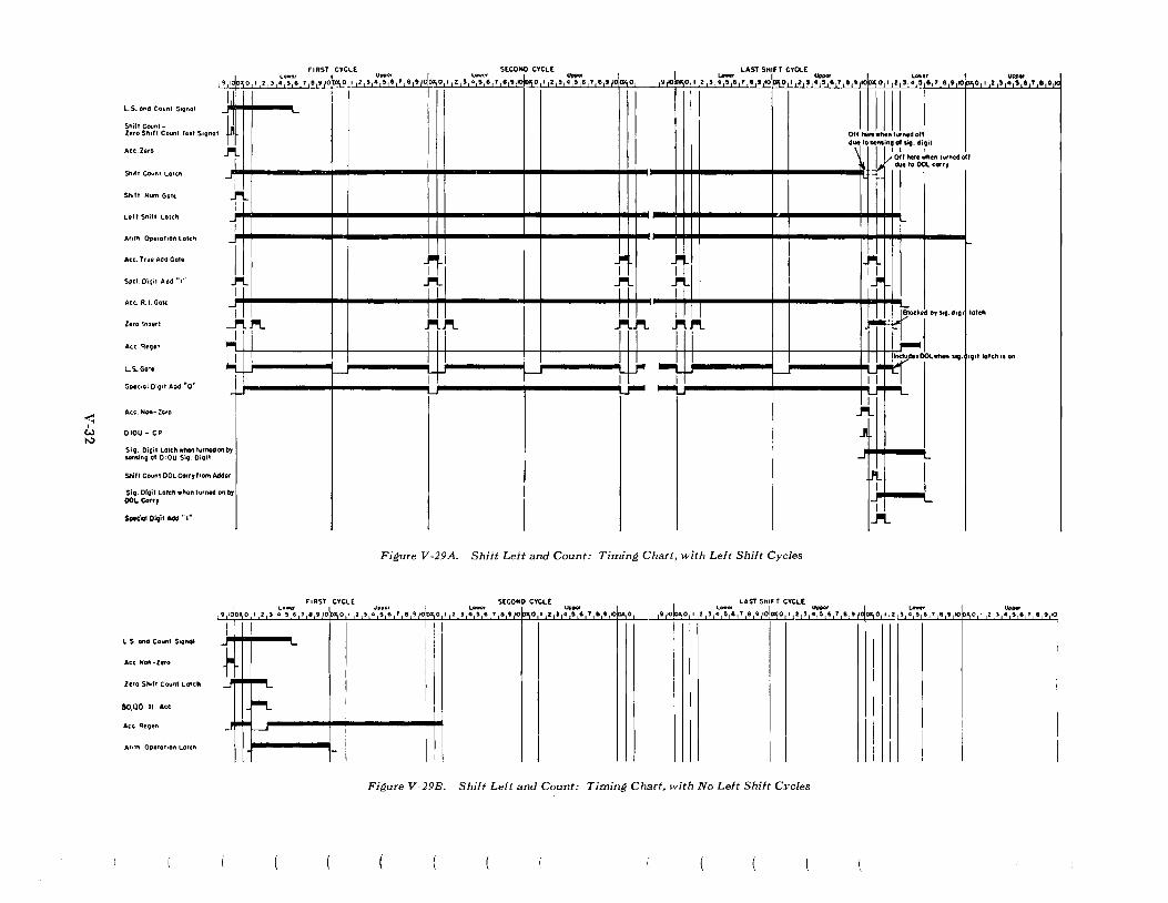
l S ond Count Sionol
Ate: Non· Zero
It'o SPlitt Counl Late"
80,00 RI Ace
Ace Regen
Ani" OP"O'lon Lole"
FIRST CYCLE SECONO CVCLE
d L._ I u •• ~ ~ ...... I "-~~o! I !2,3,4,~19ox.O~1 ,2,',4[5 1',7,8,',10 ~O~I ,2, ',4'~If$I 7 !819JI()D~~1 121'rtt~,Et7,e,,!tO~O
I'
"IO!ox"OI'121'1~61711J191101~o'l
-r1-1 ...l"'t.
tt I II ~I n n " I , 'I n...l"'t. JI'
1"tl"t J""d"\.
1'+ ~ L
Figure V-29A. Shift Left and Count: Timing Chart, with Left Shift Cycles
FIRST CTCLE SECOND CVCLE LAST SI'I'FT CYCLE
I ' .1't
I
..II
....
~ I
J"L
u_ I ' ....... r .. j • ' .. ' .. I .... pO' I ,2,',4,5,6,' 18 ,0
LD_r UDDer LowOl' Uppw 'IOOl2)4567891000ItS4!167S91O 012)45679'10 O'2S4~G78' •. lOlox.o, I ,2 t' ,;~';7617 ,8 "IIO!~O ,I 12, '1~~~6,7, 8,9 IId~ 0, I ,t I ),~~" ,8,' 11O~~O.1 .2,', ~~r6" ,., ••• '
.... '-
1 - ~
-Me II III !-
Figure V-29B, Shift Left and Count: Timing Chart. with No Left Shift Cycles
I I
II
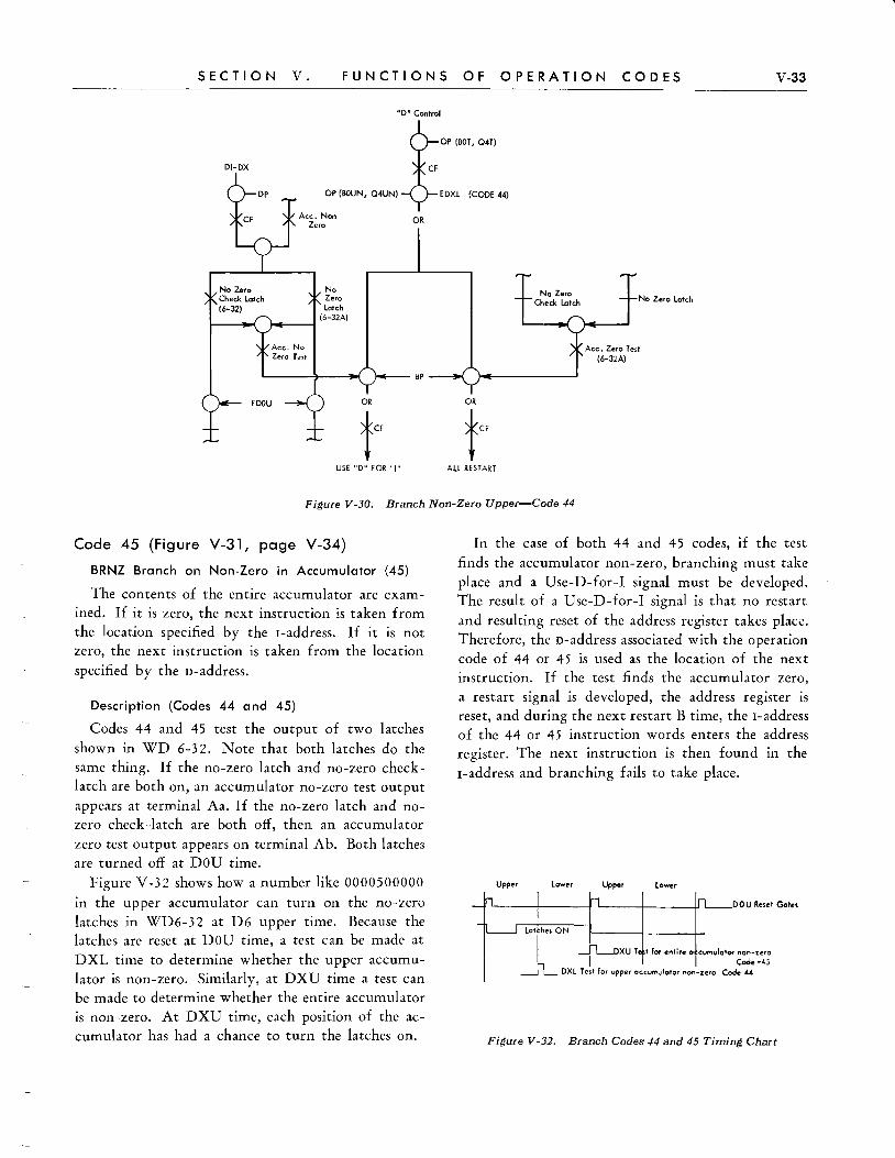
SECTION V. FUNCTIONS OF OPERATION CODES V-33
"D" Control
DI-DX
DP
No Zero Check latch (6-32)
OP (BOUN, 04UN)
Ace. Non Zero
No Zero Lctch
~_--1 (6-32A)
EDOU
Ace. No Zero T e$t
OR
USE "D" fOR "I"
OP (BOT, 04T)
EDXl (CODE 44)
OR
BP
OR
ALL RESTART
No Zero Check latch No Zero Latch
Ace. Zero Test (6-32A)
Figure V-30. Branch Non-Zero Upper-Code 44
Code 45 (Figure V-31, page V-34)
BRNZ Branch on Non-Zero in Accumulator (45)
The contents of the entire accumulator are examined. If it is zero, the next instruction is taken from the location specified by the I-address. If it is not zero the next instruction is taken from the location , specified by the D-address.
Description (Codes 44 and 45)
Codes 44 and 45 test the output of two latches shown in WD 6-32. Note that both latches do the same thing. If the no-zero latch and no-zero checklatch are both on, an accumulator no-zero test output appears at terminal Aa. If the no-zero latch and nozero check-latch are both off, then an accumulator
zero test output appears on terminal Ab. Both latches are turned off at DOU time.
Figure V-32 shows how a number like 0000500000
in the upper accumulator can turn on the no-zero latches in WD6-32 at D6 upper time. Because the latches are reset at DOU time, a test can be made at DXL time to determine whether the upper accumulator is non-zero. Similarly, at DXU time a test can be made to determine whether the entire accumulator is non-zero. At DXU time, each position of the accumulator has had a chance to turn the latches on.
In the case of both 44 and 45 codes, if the test
finds the accumulator non-zero, branching must take place and a Use-D-for-I signal must be developed. The result of a Use-D-for-I signal is that no restart
and resulting reset of the address register takes place. Therefore, the D-address associated with the operation code of 44 or 45 is used as the location of the next instruction. If the test finds the accumulator zero, a restart signal is developed, the address register is reset, and during the next restart B time, the I-address of the 44 or 45 instruction words enters the address register. The next instruction is then found in the
I-address and branching fails to take place.
Upper lower lower
_In In Ifl-DOU Re.et Gate.
-I~Lat he. ON
~XU T4 t for entire a cU"Iulot
I ----1L DXL Test for upper accumulator non-zero C
or non-zero Code -45
ode 44
Figure V-32. Branch Codes 44 and 45 Timing Chart

0000
I ReHo,'A C
II
-
CONTROL COMMUTATOR OPERATION, .5 Code BRNZ
.Auv~ thot the 650 is operating with the following series of program Jtep': .. )(Xu 0003 45 00060008
Auume the Accumulator h Zero
0001 0002 0003 0004 0005 0006 0007 0008
Restort A r- Restort A Restort A
OXBP OXCP
Restort B Restort B Restart B
j 1 -1 I AOOR Stort RI OP AOOR AOOR Enable Read-In
10003 I ~! 00061 I 0008 I 1 Stort RI n Stort RI P I-
0 RIPS RIPS
0
~tJ (RI 45 ,0006 0008 ) (It I contenh of 0008)
n One Word Early n "I" Alto,"ati01 . L
"I" Control
I L...--
Ir-"0" Alternation
"0" Control h i
EOXU '0" 1 f;nd, Accum)alo, = Z~ L I Auume the Accumvlot?r i~ non-zero
Restart A
~ U,o "0" fo,1 "I" ';9nol
Restort A ]
Re~tort B
j j OP AOOR
Enable RI
[ill 10006 1
Stort RI 0 RIPS
(RI con lent> of 0006)
n One Word Early n "I" Alte,"o,;oi II i I
"I" Control II
I "0" A hemotion II II II
J "0" Control h h EOXU test finds Accumulator;;; non-zero
I Figure V -31. Control Commutator Operation-Code 45
V-34

SECTION V. FUNCTIONS OF OPERATION CODES V-3S
Code 46
BR MIN (46)
The sign of the accumulator is examined. If it is positive, the next instruction is taken from the location specified by the I-address. If it is negative, the next instruction is taken from the location specified by the n-address.
Description-Code 46
Code 46 tests whether the accumulator plus sign or accumulator minus sign latch is on. These latches were set up when the last accumulator entry was
made. No waiting for a special test time is required and the test is timed by the appearance of D control. If the plus latch is on, a restart is developed. If the minus latch is on, a use-D-for-I signal is developed.
Circuits for Code 46
1. On WD7-2IAL, the D control 46 code signal is switched with the output of the accumulator plus
latch to give a restart signal. 2. The D control 46 code signal is switched with
the output of the accumulator minus latch to give a Use-D-for-I signal.
Code 47 (Figure V-33)
Objective
Examine the condition of the overflow circuit. If it is not set (indicating that no overflow has occurred), the next instruction is taken from the location specified by the I-address. If it is set (indicating that an overflow has occurred) , the next instruction is
taken from the location specified by the n-address.
Description Code 47 (WD 7-10, WD 7-21)
Code 47 tests for an accumulator overflow condi
tion as indicated by the status of the overflow sense
latch (WD7-2IAL). If this latch is off, a restart is signaled. If it is on, the next DI turns it off and a
capacitor-coupled cathode follower pulse when it goes
off is the use-D-for-I signal.
Test Codes (90's) (Figure V-34)
Objectives
The 90's codes test the digit posltlons of the distributor for eight's. For example, if a 93 code is programmed, a test is made of the D3 position of the
WD 7-21 AL
Overflow Sense Off
"D" Control
OP (BOT, Q4T)
OP B5UN
OP Q2U N (Code 47)
Dl
D5 Overflow Sense latch
All Restart Use 110" for 11111
Code 47 Branch On Overflow
Figure V-33. Branch on Overflow-Code 47
liD" Control
~----~OR--------------~.~OR
1'Ml7-2IAUI
D;" OT (BS. Q4)
D5 or DIO
CP
Restart Use "0" For "I"
Figure V-34. Branch on "8" in Position 1-IO-Code 90's
V-36 IBM 650
distributor to determine whether it contains an 8
or a 9. If the third position contains a digit 9, the next instruction is taken from the location specified by the I-address. If the third position contains a digit 8, the next instruction is taken from the location specified by the D-address. If the third position contains a digit other than an 8 or 9, it is an error and
the calculator will stop.
Description Code 90-99
During the word interval following the appearance of D control, the operation code value is switched with digit timing pulses to produce a test gate. The digit interval during which the test gate is developed depends on the value of the operation
code such that code 90 produces a D 1 0 code 91 produces a D1
code 92 produces a D2 code 93 produces a D3 code 94 produces a D4 code 95 produces a D 5 code 96 produces a D6 code 97 produces a D7 code 98 produces a D8 code 99 produces a D9
This test gate is then separately switched with the distributor B5 -Q3 on-time outputs and the B5 -Q4 ontime outputs to develop either a use-D-for-l signal if the distributor contains an 8, or a restart signal if the distributor contains a 9.
MULTIPLICATION (Code 19)
(Figures V-35 to V-41)
THE contents of the location specified by the Daddress are multiplied by the contents of the upper half of the accumulator. The twenty-digit product is developed in the accumulator, and the multiplier
is lost. On a code 19 it is possible to process a maximum
of a ten-digit multiplier with a ten-digit multiplicand to develop a twenty-digit product. The multiplication operation is a combination of left shift and true add
cycles.
Functions, Objectives and Circuits (Code 19) Descri ption
1. The multiplier is in the upper accumulator as
the result of a previous operation.
2. The multiplicand is put in the distributor from storage (part of the multiply operation).
3. The entire accumulator except the DXL and DOL positions is shifted left one place. During this shift, the high-order position of the accumulator, which is the multiplier digit, is shifted into the DXL position of the accumulator. The multiplicand is added into the lower accumulator the number of times indicated by this multiplier digit. If the multiplier digit is a zero another left shift is signaled.
4. Step 3 is repeated ten times, once for each multiplier digit. A count of these shifts will be kept in the DoL position to set up end-of-multiply.
5. The twenty-digit product is given the proper sign according to the signs of the factors.
The lower accumulator must be clear for this operation. If the lower accumulator contains some number at the start of a multiplication, the final result will have the absolute value of that number added to the ten high-order positions of the absolute value of the product and this result will be given the sign of the product. Thus, much care must be taken to assure that the lower accumulator is clear before a multiplication. Figure V -35 shows the values in the accumulator during the cycles of a typical mutiply operation.
General Circuit Action Code 19
The first cycle of a multiply operation is a multiPly-divide left shift cycle which is controlled by the multiply latch and the multiply-divide left shift latch, resulting in shifting the multiplier one position to the left in the accumulator. This places the high-order digit in the DXL position. Any partial product that may be in the lower accumulator is, of course, also shifted left one position, because any shift involves the whole accumulator. Also, on a multiply-divide left shift cycle, the shift count number in the accumulator DoL position is advanced by one. This number is zero at the start of the operation, so it becomes one during the first part of the first multiply add cycle.
At DXL time of each multiply cycle the adder output is tested for zero or non-zero. When this test is made at DXL of the cycle following a multiply-divide

~ W 'I
.. __ . CYCLE
1 2
~
5 6 7 A 0
10 11 12 13 14 15 16 17 18 19 20 21 22 23 24 25 26 27 2B 29 30
M<ltialle, Left Shift
Add Add Add Add Add
~ .. ~~ Add l S Add , S Add Add Add L S Add Add Add Add Add Add Add Add L S Add Add Add Add
10 9 8 7 6 5 4 3 2 lOX
Is 2 113 18 7 4 1 6 9 2 1 3 8 7 4 1 6 9 0
I B 7 9 0 2 1 3 8 7 4 1 9 0 2 1 3 8 '7 4 1 6 9 0 2 1 3 8 7 4 1 6 9 1 2 1 3 8 7 4 1 6"9 1 1 3 8 7 4 1 6 9 1 5
13 7 4 9 1 3 8 7 4 1 6 9 1 6 3 8 7 4 1 6 9 1 6 5 3 8 7 4 1 6 9 1 6 5
7 4 1 6 9 1 6 6 8 7 4 1 6 9 1 6 5 7 8 7 4 1 6 9 1 6 5 7 8 7 4 1 6 9 1 6 5 7 7 4 1 6 9 1 6 5 7 6 7 4 1 6 9 1 6 5 7 6 7 4 1 6 9 1 6 5 7 7 7 4 1 6 9 1 6 5,7 7 7 4 1 6 9 1 6 5 7 7 7 4 1 6 9 1 6 5 7 8 7 4 1 6 9 1 6 5 7 8 7 4 1 6 9 1 6 5 7 8 7 4 1 6 9 1 6 5 7 9 4 1 6 9 1 6 5 7 9 0 4 1 6 9 1 6 5 7 9 1 4 16 9 7 9 4 1 6 9 1 6 5 7 9 1 4 1 6 9 1 6 5 7 9 2
TYPICAL MULTIPLY OPERATION
10 Digit MlJltiplicand 10 Digit Multiplier 20 Digit Product
Shih count
I Add count 10 9 8 7 6 5 4 3 2 lOX
o 0 o 0 o 0 o 0 0 o 0 0 o 0 o 0 o 0 o 0 0 010
7 9 4 21n 9 6 3 9 6 9 6 4 1 B I 4 9 5 3 9 5 4 4 6 2 713 2 7 1 9 3 9, 2 8 3 612 5 B 9 9 2 4 1 0 4 1 1 8 9 9 2 4 1 o 4 5 0 2 0 2 7 2 2 16 912 5 3 5 2 1 0 6 8 6 8 2 1 3 5 2 1 o 6 8 6 8 0 3 0 6 7 o 0 9 1 6 8 8 9 3 1 7 0 091 8 9 040 o 1 8 9 o 1 7 0 9 9 4 3 3 3 6 8 8 6 5 3 o 8 4 2 6 5 4 8 7 1 3 5 1 4 1 5 4 8 7 1 3 5 1 7 0 5 0 8 6 6 6 9 8 3 3 7 9 5 8 1 8 4 6 8 3 1 5 8 8 5 7 5 0 2 6 6 7 9 7 9 7 5 6 8 2,0 6 ,5 2 8 o 0 65 15 1 3 8 6 3 7 6 2 1 5 5 4 4 5,6 6 2 2 4 4 2 4 5 3 7 : 7 4 6 o 7 2 6 3 3 5 2 o 9 2 5 9 2 o 8 4 2 5 1 9 2 5 9 2 0 8 4 2 0 6 0 2 4 3 9 o 5 6 6 2 '9 6 7
' 11 R 9 418 8 6 879 8 7 5 3 o 4 7 6 5 1 ~7 8 6 0 1 2 5J.6 6 4
.. __ . CYCLE
31 32 33 34 3S 36 37 3B 39 40 41 42 43 44 45 46 47 48 49 50 51 52 53 54 55 56 57 58
3179848209 5213874169
165793284382460 13321
IQYH76543210X
Add 4 1 6 9 1 6 5 7 9 2 Add 4 1 6 9 1 6 5 7 9 2 Add 4 1 6 9 1 6 5 7 9 3 l S 1 6 9 1 6 5 7 9 3 1 Add 1 6 9 1 6 5 7 9 3 1 Add 1 6 9 1 6 5 7 9 3 2 Add 1 6 9 1 6 5 7 9 3 2 Add 1 6 9 1 6 5 7 9 3 2 L S 6 9 1 6 5 7 9 3 2 7 Add 6 9 1 6 5 7 9 3 2 8 L S 9 1 6 5 7 9 3 2 8 2 Add 9 I 6 5 7 9 3 2 8 2 Add 9 1 6 5 7 9 3 2 8 2 Add 9 1 6 5 7 9 3 2 8 3 Add 9 1 6 5 7 9 3 2 8 3 Add 9 1 6 5 7 9 3 2 8 3 Add 9 1 6 5 7 9 3 2 8 4 L S 1 6 5 7 9 3 2 8 4 0 Add 1 6 5 7 9 3 2 8 4 1 Add 1 6 5 7 9 3 2 8 4 1 Add 1 6 5 7 9 3 2 8 4 1 Add 1 6 5 7 9 3 2 8 4 2 Add 1 6 5 7 9 3 2 8 4 2 Add 1 6 5 7 9 3 2 8 4 2 Add 1 6 5 7 9 3 2 8 4 3 Add 1 6 5 7 9 3 2 8 4 3 Add 1 6 5 7 9 3 2 3 4 3 Stop_ 1 6 5 7 9 3 2 8)4 3
Figure V -35, Accumulator Values during Typical Multiplication
r 10 9 8 7 6 5 4 3 2 lOX
5 1 5 8 4 4 9 4 6 5 6 3 8 3 3 8 2 9 7 6 7 4 6 2 1 5 1 8 1 4 5 8 B 3 6 1 5 1 8 1 4 5 8 8 3 0 7 0 8 3 6 1 3 0 7 0 3 9 7 4 1 5 4 1 1 5 5 2 4 8 7 3 4 7 2 1 o 0 3 4 5 7 7 2 7 9 o 0 e 5 1 6 16 7 9 0 0'8 5 1 6 6 6 0 8 0 2 1 8 8 3 6 4 8 6 9 8 1 1 8 8 3 6 4 8 0 9 0 9 0 5 0 6 3 4 9 6 8 9 9 9 6 8 2 4 3 3 4 5 1 o 8 9 5 1 4 2 3 1 9 3 3 1 7 9 4 4 6 o 3 o 4 1 5 2 6 9 3 7 7 8 2 8 8 9 7 3 5 9 2 o 9 6 2 7 3,7 9 4 49 1 9 6 2 7 3 7 9 4 4 0 o 0 2 8 o 7 2 2 7 6 4 9 o 9 5 9 8 7 o 7 5 8 5 8 o 8 9 1 6 6 9 2 4 0 6 7 o 7 2 3 4 6 7 7 2 2 7 6 o 6 5 5 2 6 6 2 o 4 8 5 o 5 8 7 o 6 4 6 8 6 9 4 o 4 1 8 B 6 3 1 6 9 o 3 o 3 5 0 6 6 1 6 5 1 1 2 o 2 8 2 4 6 o 1 3 3 2 1 o 1 8 2 4 6 o 1 3 3 2 1 o 0
Shift CO""t Add count
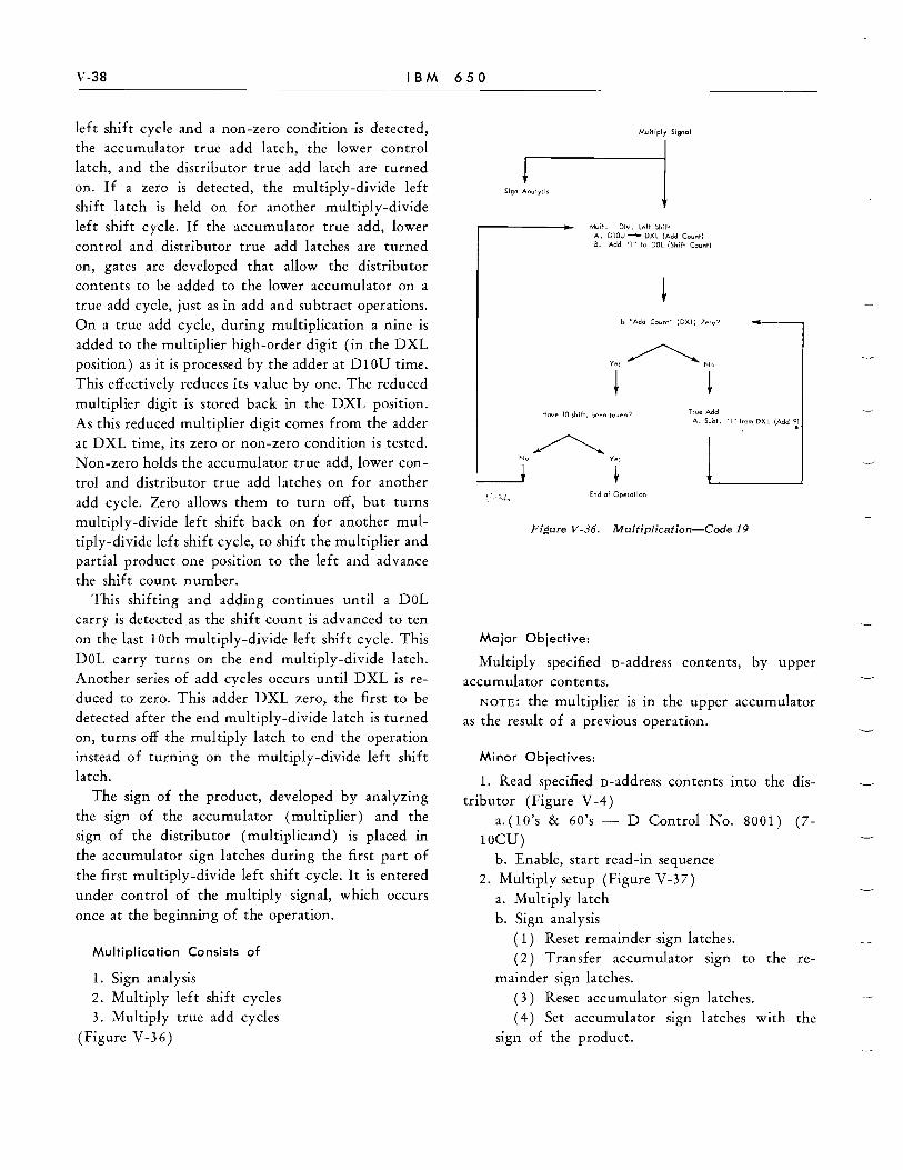
V-38 IBM 650
left shift cycle and a non-zero condition is detected, the accumulator true add latch, the lower control latch, and the distributor true add latch are turned on. If a zero is detected, the multiply-divide left shift latch is held on for another multiply-divide left shift cycle. If the accumulator true add, lower control and distributor true add latches are turned on, gates are developed that allow the distributor contents to be added to the lower accumulator on a true add cycle, just as in add and subtract operations. On a true add cycle, during multiplication a nine is added to the multiplier high-order digit (in the DXL position) as it is processed by the adder at DI0U time. This effectively reduces its value by one. The reduced multiplier digit is stored back in the DXL position. As this reduced multiplier digit comes from the adder at DXL time, its zero or non-zero condition is tested. Non-zero holds the accumulator true add, lower control and distributor true add latches on for another add cycle. Zero allows them to turn off, but turns multiply-divide left shift back on for another multiply-divide left shift cycle, to shift the multiplier and partial product one position to the left and advance the shift count number.
This shifting and adding continues until a DOL carry is detected as the shift count is advanced to ten on the last 10th multiply-divide left shift cycle. This DOL carry turns on the end multiply-divide latch. Another series of add cycles occurs until DXL is reduced to zero. This adder DXL zero, the first to be detected after the end multiply-divide latch is turned on, turns off the multiply latch to end the operation instead of turning on the multiply-divide left shift latch.
The sign of the product, developed by analyzing the sign of the accumulator (multiplier) and the sign of the distributor (multiplicand) is placed in the accumulator sign latches during the first part of the first multiply-divide left shift cycle. It is entered under control of the multiply signal, which occurs once at the beginning of the operation.
Multiplication Consists of
1. Sign analysis 2. Multiply left shift cycles 3. Multiply true add cycles
(Figure V-36)
Sign Anolysil
Multiply Signal
j Mult. Diy. left Shift
A. DIOU - DXl (Add Count) S. Add "I" to DOL (Shift Count)
Is "Add Count" (DXl) Zero?
~ Yes No
~ ~ Have 10 m ifts been taken? True Add
~ No Yes
End of Operation
A. Sub •• "I" from DXL (Add 9) .
Figure V-36. Multiplication-Code 19
Major Objective:
Multiply specified o-address contents, by upper accumulator contents.
NOTE: the multiplier is in the upper accumulator as the result of a previous operation.
Minor Objectives:
1. Read specified o-address contents into the distributor (Figure V -4 )
a.(IO's & 60's - D Control No. 8001) (7-IOCU)
b. Enable, start read-in sequence 2. Multiply setup (Figure V-37)
a. Multiply latch b. Sign analysis
( 1) Reset remainder sign latches. (2 ) Transfer accumulator sign to the re
mainder sign latches. ( 3) Reset accumulator sign latches. ( 4) Set accumulator sign latches with the
sign of the product.
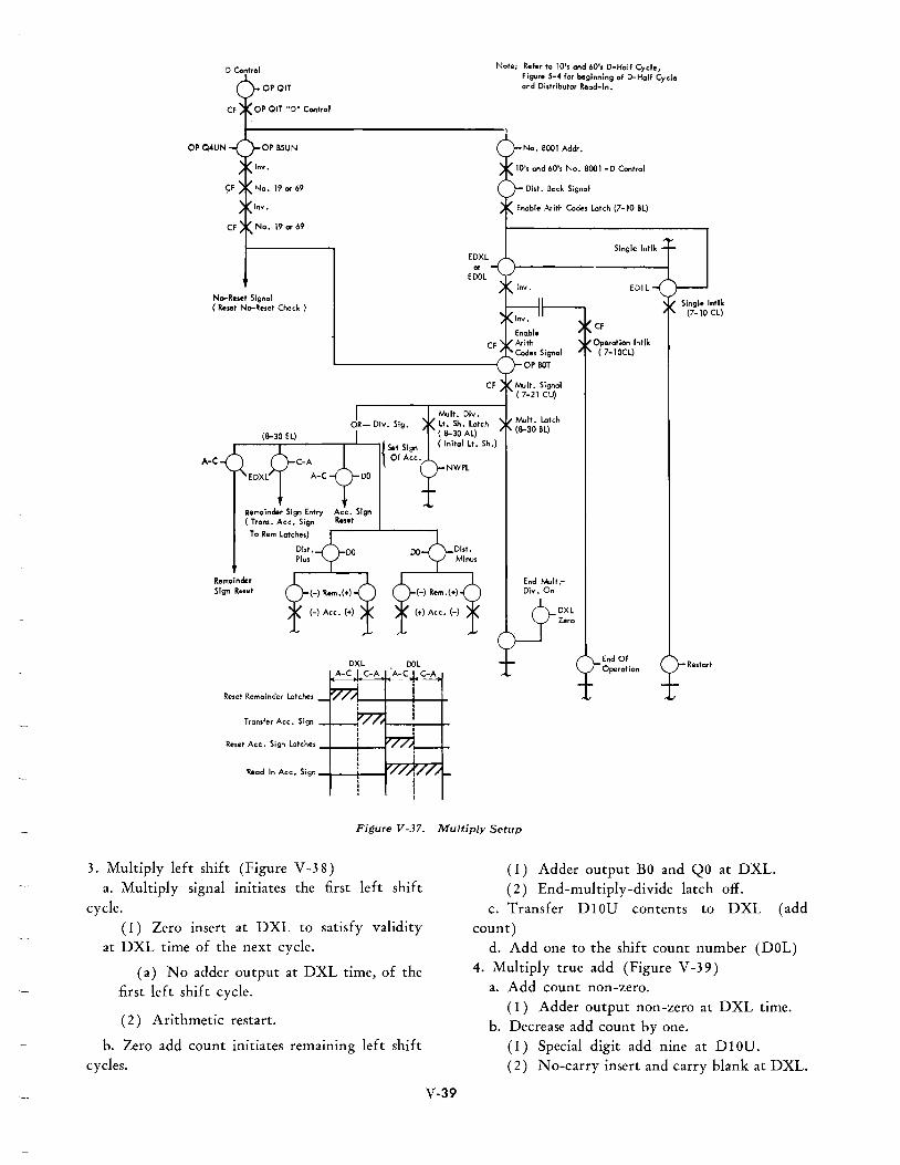
D Control
OPQIT
OP QIT "D" Control
OPQ4UN OP B.5UN
No--Reset Signal ( Reset No-Reset Check)
A-C
Remainder Sign Entry Ace. Sign ( Trans. Ace. Sign Reset
EDXL 0(
EDOL
Note; Refer to la's and 60's O-Holf Cycle, figure 5-4 f", beginning of D-Half Cycle and Distributor Read-In.
No. 8001 Addr.
10's cnd 60's No. 8001 -D Control
Oist. Back Signal
Enable Arith Codes lotch (7-10 BL)
CF
Operation Intlk ( 7-10CL)
To Rem Latches) ....-----'-----.
Remainder Sign Reset
Reset Remainder latches
Transfer Ace. Sign
Reset Ace. Sign Latches -+_-+-_-/
Read In Ace. Sign -+_-+_-1
Figure V-37.
3. Multiply left shift (Figure V-38) a. Multiply signal initiates the first left shift
cycle. (1) Zero insert at DXL to satisfy validity
at DXL time of the next cycle.
(a) No adder output at DXL time, of the first left shift cycle.
( 2) Arithmetic restart.
b. Zero add count initiates remaining left shift cycles.
End Mull.DiY'. On
DXL Zero
End Of Operation Restart
Multiply Setup
V-39
( 1) Adder output BO and QO at DXL. (2) End-multiply-divide latch off.
c. Transfer DIOU contents to DXL (add count)
d. Add one to the shift count number (DOL) 4. Multiply true add (Figure V-39)
a. Add count non-zero. (1) Adder output non-zero at DXL time.
b. Decrease add count by one. (1) Special digit add nine at DI0U. (2) No-carry insert and carry blank at DXL.

EDXL
Add "I" DXL
Sig. Digit Off
Ace. R.I. Gate
.------____ "0" Insert
.------"0" Insert On Initial L.S. Only ( T a Satisfy Validity )
First l.S. Cycle Initiated By - Multiply Signal Remaining l,S, Cycles Initiated By - Multiply On, End MID Off And DXL Z.,O.
Mult. Sig. (7-21 CU) ( Initiates First left Shift Cycle)
EDXL DXL
( Increase Shift Count Number
By One)
Left Shift Gate
Zero Insert ( 8-30 EU) ( Initiates Remaining loS. Cycles)
OR
CF Any Shift ( 8-30 DU )
Neg.Sh. Num. Gate
OR
Mult. o;v. Lt. Sh. Latch ( 8-30 AL )
DXL EDIL
OR
Ace. Regen Off Arith. Operation Latch On
Ace. True Add Gate
DXL
No-Carry Insert and Zero Insert
le'ft Add "O's"
NWPL
Shift Except Gote @DXL ( 8-30 BU )
No Camp Ace. or Dist.
EDXL ~ L EooL
OR
No-Carry Insert (8-30 EU )
Figure V-38. Multiply Left Shift Cycle
V-40
Ace. R.I. Gote
Spec. Digit Add "I" DXL
Spec. Digit Add "0" Except DXL
No-Carry Inserts DOL, DXL & OIL
End MID Off ( 8-30 AL)
Mult. Latch (B-30 BL)
Ace. Read-In Gate
( 8-30 CU )
End Mult.Div. On
Ace.Regen Oli (8-30 CU)
09
Restort
NEDX
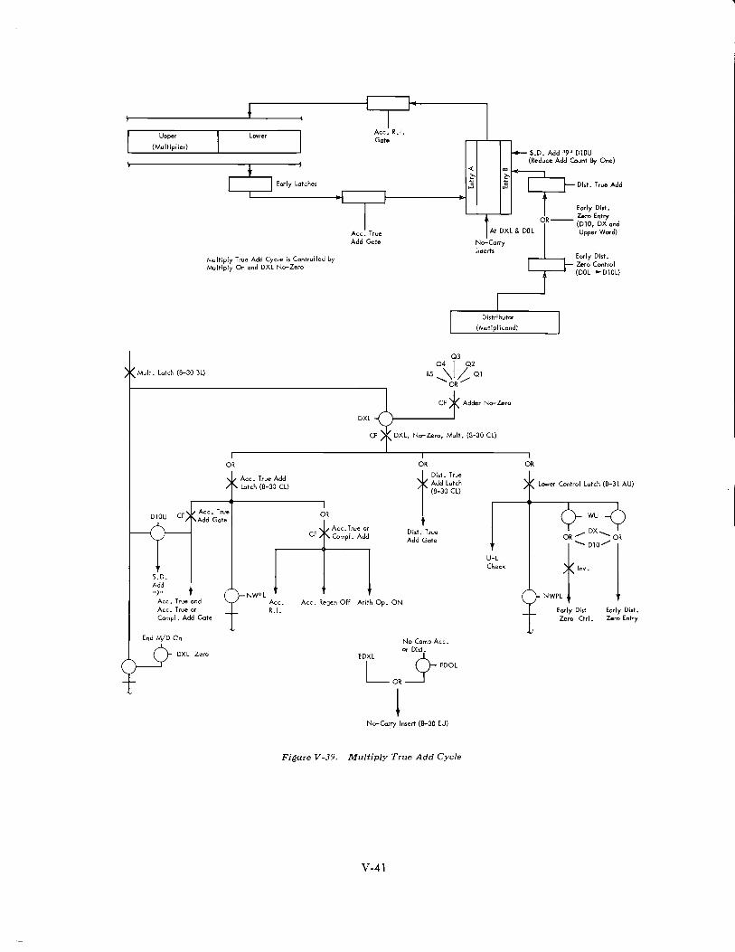
Upper
(Multiplier)
lower Ace. R.I. Gate
« ~
Early Latches ~
~=------------[~------l
Multiply TN. Add Cycle is Controlled by Multiply On and DXL No-Zero
Ace. True Add Gale
03
No-Carry Inserts
(Mutiplicand)
Mult. Lotch (8-30 BL) 04 I 02
B5 '\ /. 01 ........ OR/
OR
Dl0U CF Ace. True Add Gate
S.D. Add "9"
Ace. True and Ace. True or Compl. Add Gate
End M/D On
DXL Zero
Ace. True Add Lotch (8-30 CL)
NWPL Ace. R.I.
OR
CF
DXL
Ace.True or Compl. Add
OR
Add Lotch (8-30 CL) t Dist. True
Dist. True Add Gate
Ace. Regen Off Arith Op. ON
No Comp Ace. or Dist.
EDXL ~
LOR~ EDOL
No-Corry Insert (8-30 EU)
Figure V -39. Multiply True Add Cycle
V-41
Adder No-Zero
U-L Check
OR
Dlst. T Ne Add
Early Dist. Zero Control (DOL -- DlOL)
Lower Control Latch (8-31 AU)
°tR ::: ~;O-::: °IR Inv.
NWPL
Eorly Dist Zero Ctrl.
Eorly Dist. Zero Entry

V-42 IBM 650
Turn Operation Inlli<.. Off
Arlit.. Operation lntch (8~30DU)
"XL
'"-9-"0 PX.LZeroJ / Cf
(8-3(BL)
"'''''it.lc:Itcr. (8-30BL)
Tum ALe. Regen. On
Figure V -40. End of Multiply
5. Allow control commutator to advance (Figure
V-40) . a. Turn operation interlock off.
(1) End-of-operation. Refer to Figure V -41 for multiply sequence chart,
pages V-44 and V-45.
DIVISION (Code 14)
(Figures V-42 to V-52)
THE dividend must be in the accumulator as the result of a previous operation. The divisor is placed in the distributor from the D-address location specified in the divide instruction. The quotient will be developed in the lower accumulator and its sign will be in the accumulator sign latches. The remainder
will be in the upper accumulator and its sign will be in the remainder sign latches. Either half of the accumulator with its corresponding sign may be stored.
Principles of Division Division is accomplished by taking a left shift cyci<:
on the first cycle of divide, then subtracting the divisor (distributor) from the upper accumulator until a dividend sign change indicates it has been subtracted one too many times. Each time the divisor is subtracted with no change in dividend sign, a one is
added to the quotient (Dl Lower Acc.). When a dividend sign change occurs, the divisor is added once to the upper accumulator to correct for the over
draw. The reduced dividend and partial quotient are then shifted one place to the left. The divisor is subtracted from the reduced dividend until a dividend sign change occurs. Each time the divisor is subtracted with no change in dividend sign, a one is added to the quotient (Dl Lower Acc.).
This process is repeated for ten shifts in all. On the tenth left shift a DOL carry turns on the endmultiply-divide latch. The divisor is subtracted <!s before from the dividend until a dividend sign change occurs. A one is added to the quotient for each cycle the divisor is subtracted with no change in dividend sign. The divisor is added once to the dividend to correct for the overdraw and signals for a left shift. This time, however, because the end-multiply-divide
latch is on, instead of left shifting we end division (turn divide latch off).
Figure V -42 illustrates the concept of division, using
an abbreviated accumulator with eight positions for simplicity. The problem 1440 -7-" 12 = 120 is used.
The first cycle of a divide operation is a multiplydivide left shift cycle. This clears the D1L accumu
lator position for possible quotient digit entries during the first shift. In the case of the eight-position accumulator shown, only four shifts are possible. In actual practice the 650, with its 20-digit accumulator, uses ten shifts for each division. The number of shifts is counted, as in other shifting operations, and the count retained in the accumulator DOL position. This shift count action is not shown in the chart.
On any division the number of digits in the quotient is determined by the number of digits in the dividend and divisor. In the 650 the maximum number of quotient digits that can be developed is ten and is governed by the capacity of the accumulator and distributor. Thus, on any 650 divide operation, the highest significant dividend digit must be positioned in the accumulator, taking into account the number of digits in the divisor, so that no more than nine subtractions will be required on the first shift to produce a sign change.
When the dividend is not properly positioned and more than nine subtractions would be needed to cause a sign change, more than nine quotient digit one

PROBlEM: 1440 + 12 = 120
ACCUMULA TOR UPPER LOWER
D4 D3 D2 DI D4 03 02 01 OOL
Dividend 0 0 0 0 1 4 4 0 0
Shift 0 0 0 1 4 4 0 0 1
Subtract Oi .... (Upper) -0 0 1 2 0 0 0 0 1 -- --
Sign C~ange 9 9 8 9 4 4 0 0 1
Correct +0 0 1 2 0 0 0 0 1 -
0 0 0 1 4 4 0 0 1
Shift 0 0 1 4 4 0 0 0 2
Subtract Diy. (Upper) -0 0 1 2 0 0 0 0 2
No Sign Change 0 0 0 2 4 0 0 0 2
Sub'r. Div. (Upper) Enter" 1" (Lwr. ) - 0 0 1 2 0 0 0 1 2 ---
Sign Change 9 9 9 0 4 0 0 1 2
Correct +0 0 1 2 0 0 0 0 2 -
0 0 0 2 4 0 0 1 2
Shift 0 0 2 4 0 0 1 0 3
Subtr. Diy. (Upper) - 0 0 1 2 0 0 0 0 3 ----
No Sign Change 0 0 1 2 0 0 1 0 3
Subtr. Dlv. (Upper) Enter" 1" (Lwr. ) - 0 0 1 2 0 0 0 1 3
No 5 i gn Change 0 0 0 0 0 0 1 1 3
Subtr. Div. (Upper) Enter "1" (Lwr. ) - 0 0 1 2 0 0 0 1 3
Sign Change 9 9 8 8 0 0 1 2 3
Correct +0 0 1 2 0 0 0 0 3 ----- ---
0 0 0 0 0 0 1 2 3
Lost Shift 0 0 0 o I 0 1 2 0 4
Sub!r. Div. (Upper) - 0 0 1 2 0 0 0 0 4 - - - - - ---- -
Sign Chonge 9 9 8 8 0 1 2 0 4
Correct +0 0 1 2 0 0 0 0 4 --
Stop 0 0 0 0 0 1 2 0 0
Figure V -42. Division, Using an Abb[evia~ed Accumulator of Eight Positions
entries will be entered at DIL. A carry from DIL detects this condition and sets up an overflow stop.
On a multiply-divide left shift cycle the highorder dividend digit is shifted left from the D 1 OU accumulator position into the DXL accumulator position. From here it enters the adder at DI0U time on a divide subtract cycle, from the accumulator early output. The distributor contents are subtracted from the upper accumulator by the usual complement add entry.
A zero is supplied by the distributor zero entry circuit as a DXL distributor early output, to merge
with the high-order dividend digit. This zero enters as a complement on a subtract (reduction) cycle and in true form on an add (correction) cycle. When a complement number is added to a tme number, ,1
carry from the high-order position indic1tc3 that the
result is still a true number and the sign has not changed. No carry indicates that the result is complement and the sign has changed.
This principle is illustrated by Figure V -43 usmg the previous example of 1440 ~ 12 = 120.
This DXL carry or no-carryon a divide subtract
cycle is used to determine whether the following cycle will be add or subtract. When an add (correc .. tion) cycle is finally set up, its completion signals another multiply-divide left shift cycle.
On each multiply-divide left shift cycle the shift count number in the DOL accumulator position is advanced by one. This number is zero at the start of the divide operation, so it becomes zero and a DOL carry occurs on the tenth shift. After this DOL carry occurs, the completion of the next add (correction) cycle stops the operation instead of signaling a multi
ply-divide left shift cycle.
PROBLEM: 1440 i- 12 = 120
ACCUMULATOR UPPER LOWER
OXL 04 03 02 01 D4 03 02 DI OOL
Dividend 0 0 0 0 0 1 4 4 0 0
Shift 0 0 0 0 1 4 4 0 0 1
Subtr. Diy. 9 9 9 8 7 9 9 9 9 1 1 , 9 9 9 8 9 4 4 0 0 1 No Carry DXL, Sign Change
;
Correct 0 0 0 1 2 0 0 0 0 1 --
0 0 0 0 1 4 4 0 0 ·1
Shift 0 0 0 1 4 4 0 0 0 2
Subtr. Diy. Upper 9 9 9 8 7 9 9 9 9 1 2 ----- --- ---- ------ - --
Corry DXL, No Sign Change 0 0 0 0 2 4 0 0 0 2
Subtr. Diy. Upper. Enter" 1" Lwr. 9 9 9 8 7 9 9 9 1 1 2 -- ---,
No Carry DXl, Sign Change 9 9 9 9 0 4 0 0 1 2
Correct 0 0 0 1 2 0 0 0 0 2 ---
0 0 0 0 2 4 0 0 1 2
Shift 0 0 0 2 4 0 0 1 0 3
Subtr. Diy. Upper 9 9 9 8 7 9 9 9 9 1 3 -------
Corry DXL, No Sign Change 0 0 0 I 2 0 ci 1 0 3
Subtr. Diy. Upper. Enter" 1" lwr. 9 9 9 8 7 9 9 9 1 1 3
Carry DXL, No Sign Change 0 0 0 0 0 0 0 1 1 3
Subtr. Diy. Upper. Enter "I" lwr. 9 9 9 8 7 9 9 9 1 1 3 --,
No Corry DXL, Sign Change 9 9 9 8 8 0 0 1 2 3
Correct 0 0 0 1 2 0 0 0 0 3 --
0 0 0 0 0 0 0 1 2 3
Shih 0 0 0 0 0 0 1 2 0 4
Subtr. Diy. Upper 9 9 9 8 7 9 9 9 91 4
No Carry DXL, Sign Change I> 9 9 8 8 0 1 2 0 4
Correct 0 0 0 1 2 0 0 0 0 4 --
Stop 0 0 0 0 0 0 1 2 0 0
Figure V-43. Simplified Accumulator Showing Dividend Sign Change
V-43
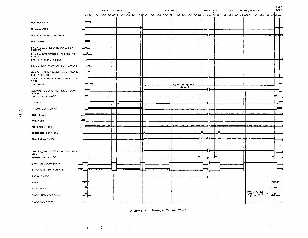
..-: ,i.. ./>..
MULTIPLY SIGNAL
M.-D.L.S. LATCH
MULTIPLY LATCH AND M-D GATE
M-D SIGNAL
DXL A-C GATE RESET REMAINDER SIGN LATCHES
OX L C-A GATE TRANSFER ACC. SIGN TO REM. LATCHES
REM. PLUS OR MINUS LATCH
DO A-C GATE. RESET ACC. SIGN LATCHES
MOL5-
FIRST CYCLE M.D.L S ADD CYCLE S ADD CYCLES LAST ADD CYCLE IN SHIFT CYCLE U L U L U L U L
OX 0 I 2 3 4 5 6 7 8 9 1 X 0 I 2 3 4 5 6 7 8 9 ox 0 1 2 3 4 5 6 7 8 9 I X 0 , 2 :3 4 5 6 7 8 9 I 2 :3 4 5 6 7 8 9 I 0 0 I 2 3 4 5 6 7 8 9 10 X 0 I J
I I III II H-ti'
-H-l -111 1111 III II Illf
~' M-D PLUS OR M-D MINUS SIGNAL CONTROLLED BY DlST. SIGN
~r-'J
ACCPLU5 OR MINUS SIGN LATCH(PRODUCT SIGN)
ZERO INSEf1T
ACC.TR"E ADD GATE AND TRUE OR COMP ADD GArE
SPECIAL DIGIT ADD "I"
L.S. GATE
SPECIAL DIGIT ADD "0"
ACC.R.LGATE
ACC.REGEN
ARITIi. OPER. LATCH
ADDER NON-ZERO DXL
ACC. TRUE ADD LATCH
LOWER CONTROL LATCH AND U-L CHECK GATE
SPECIAL DIGIT ADD "9"
EARLY D15T. ZERO ENTRY
E.\RLY DlST ZERO CONTROL
END M-D LATCH
NEAP
ADDER ZERO DXL
ADDER ZERO DXL SIGNAL
ADO!:R CO L CARRY
I
~ II i [~
Ii _~ __ ....... UP HERE DUE TO Ace. TRUE _
ADD LATCH L_ .. __ l-L
f-
~
4J 14J III II . III ,.' III II ~.
--
II ill II~ II II~~ II II II III 11'1 II I i I " Ii I II ~
~ ~. ~tl 1t1 fl iE I I II I I
* TuRN ON M.-O.L.S. ---i LATCH WHEN END ---.,. M-D OFF
Figure V -41. Multiply Timing Chart
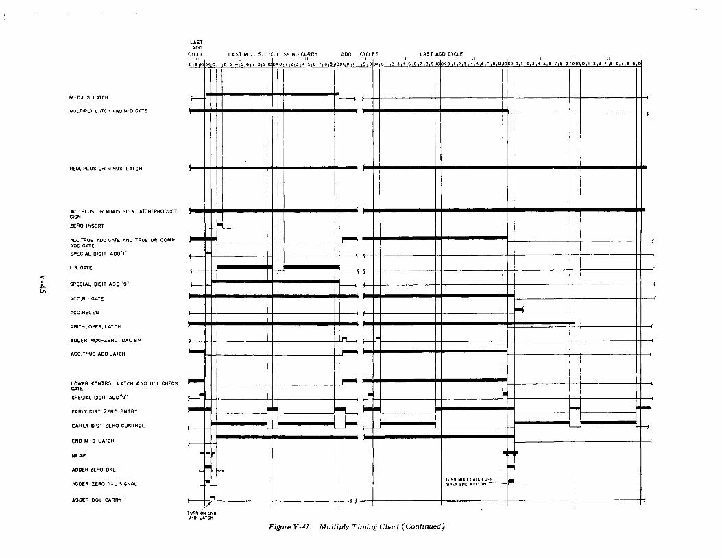
-<
M.-D.L.S. LATCH
MULTIPLY LATCH AND M-D GATE
REM. PLUS OR MINUS LATCH
ACC.PLUS OR MINUS SIGN LATCH! PRODUCT SIGN)
ZERO INSERT
ACC.TRUE ADO GATE AND TRUE OR COMP ADO GATE
SPECiAl DIGIT ADD .... '
L.S. GATE
~ SPECiAl DIGIT. ADD ·0" (,n
ACC.R.LGATE
Ace.REGEN
ARITH. OPER, LATCH
ADDER NON-ZERO DXL BP
ACC TRUE ADO LATCH
LOWER CONTROL LATCH AND U-L CHECK GATE
SPECIAL DIGIT ADO "9"
EARLY OIST. ZERO ENTRY
EARLY OIST ZERO CONTROL
END M-O LATCH
NEAP
ADDER ZERO OXL
ADDER ZERO OXL SIGNAL
ADDER DOL CARRY
LAST ADO
CYCLE LAST M.O.L.S. CYCLE SH NO CARRY ADD CYCLES LAST ADD CYCLE U L U L
gU,OOX 0\1 {2_fi4L!) 6 7 8 9101D~O 123 4U
S 6 78 9r1CDxtO I Z :3 4L
S 6 789,1(0;'-'0 I 23 4U
5 6 7 8 9.-c 89 IOOX 0 I 2: l 456 789 I o OXiO I Z 3 4 5 6 7 E 9 I OX 0 I
S--
!
'"
1----f--
r---
,.... ..... ~ ...... f--
• I~,.
- l- f--
- rL l_ U't
}7 TURN ON END M-O LATCH
I I ,
I ~ I
I I
I I I I I !
,
i
I i I
I
I~
! I-' f------,
t---'
I ~
~I-- .J'",
I~
~
~ ~
• "'~ ... • •• -I Ij.. I I L-I L I- ---' L~
-r+ - r-L
TU~N MULl L.,ATCH OFF'
~ WMEN E:NO M-O ON ~
Figure V-41. Multiply Timing Chart (C;ontinued)

V-46 IBM 650
ACC CYCLE
B :~ '" 0 Cl.~ .. 1=1
~~ ~ '> '5,15 :E"O
I
..J >< 0
UPPER
TYPICAL DIVIDE OPERATION 20 Digit Dividend 10 Digit Divisor 10 Digit Quotient 10 Digit Remainder
LOWER Xl0 9 8 7 6 5 4 3 2 lOX 10 9 8 7 6 5 4 3 2 1 0
, Divldend- 0 I 6 5 7 9 3 2 8 4 3 9 7 2 I 3 8 4 2 I 6 0 2 Shift I 6 5 7 9 3 2 8 4 3 9 7 2 I 3 842 I 6 o I 3 Subtract I I 3 6 5 4 5 4 2 7 0 7 2 I 3 842 I 6 o I 4 Subtract 0 6 I 5 1 5 8 o I o I 7 2 I 3 842 I 6 I I 5 Subtract 0 o 9 3 7 7 0 5 9 3 2 7 2 I 3 842 I 6 2 I 6 Subtract 9 5 7 2 3 8 3 1 7 6 3 7 2 I 3 842 I 6 3 I 7 Add 0 o 9 3 7 7 0 5 9 3 2 7 2 I 3 8 4 2 I 6 3 I 8 Shi ft 0 9 3 7 7 o 5 9 3 2 7 2 1 3 8 4 2 I 6 3 0 2 9 Subtract 0 4 I 6 3 I 8 5 I 5 8 2 I 3 8 4 2 I 6 3 0 2
10 Subtract 9 8 9 4 9 3 1 1 0 8 9 2 I 3 8 4 2 I 6 3 1 2 II Add 0 4 I 6 3 I 8 5 I 5 8 2 I 3 8 4 2 I 6 3 I 2 2 Shi ft 4 I 6 3 I 8 5 I 5 8 2 I 3 8 4 2 I 6 3 I 0 3
I~ S:Jbtmct 3 6 4 I 7 9 7 7 4 I 3 I 3 .s 4 2 I 6 3 I 0 3 14 Subtract 3 I 2 o 4 1 0 3 2 4 4 I 3 8 4 2 I 6 3 I I 3 15 Subtract 2 5 9 9 0 2 2 9 0 7 5 I 3 8 4 2 I 6 3 I 2 3 16 Subtract 2 o 7 7 6 3 5 4 9 o 6 1 3 8 4 2 I 6 3 I 3 3 17 Subtract I 5 5 6 2 4 8 o 7 3 7 I 3 8 4 2 I 6 3 I 4 3 16 Subtract I o 3 4 8 6 0 6 5 6 8 I 3 8 4 2 I 6 3 I 5 3 19 ~~b1'2St 0 5 I 3 4 7 3 2 3 9 9 1 3 8 4 2 I 6 3 I 6 3 20 So"~fQd Q. 9 9 2 0 8 5 8 2 3 0 I 3 8 4 2 I 6 3 I 7 3 Zl----;\d] O' 5 I 3 4 I 3 2 3 9 9 I 3 S 4 2 I 6 3 i 7 3 2? S~in 5 I 3 47 f 2 3 9 9 I 3 8 4 2 I 6 3 I 704 23 $ybtroc:t 4 6 I 3 3 4 4 9 S 2 2 3 8 4 2 I 6 3 I 704 24 S vbtr~ct 4 o 9 I 9 5 7 5 6 5 3 3 8 4 2 I 6 3 I 7 I 4 25 Subtract 3 5 7 o 5 j 0 1 4 8 4 3 8 '4- 2 I 6 3 I 7 2 4 26 S ... ,btract o 4 9 I 8 2 7 3 I 5 3 8 421 6 3 I 7 3 4
-27 Suhtrac t 2 5 2 7 7 9 5 3 I 4 6 3 8 4 2 1 6 3 I 7 44 28 Sub'Teet 2 o 0 6 4 o 7 8 9 7 7 13 8 4 2 I I 754 29 S",b'roct I 4 8 5 0 2 0 4 6 o 8 3 8 4 2 I 6 3 I 76 4 l) Subtraet 0 9 6 3 6 3 3 o 6 3 9 3 8 4 2 I 6 3 I 7 7 4 31 Subtract 0 4 4 2 2 4 5 6 4 7 0 3 8 4 2 1 6 3 I 784 32 Subtract 9 9 2 o 8 5 8 2 3 o I 3 8 4 2 1 6 3 1 794 33 Add 0 4 4 2 2 4 5 6 4 7 0 3 a 4 2 I 6 3 1 794 34 Shi ft 4 4 2 2 4 5 6 4 7 o 3 84 2 I 6 3 1 7 905 35 Subtrat;;t 3 9 0 1 0 6 9 o 5 3 4 842 I 6 3 1 7 9 0 5 36 Subtract ~ 3 7 9 6 a 1 6 3 6 5 a 4 2 I 6 3 1 7 9 1 5 37 Subtract 2 a 5 8. 2 9 4 2 1 9 6 842 I 6 3 1 7 9 2 5 38 Subtract 2 3 3 6 9 o 6 8 0 2 7 a 4 2 I 6 3 1 7 9 3 5 39 Subtract I 8 I 5 5 I 9 3 8 5 8 842 1 6 3 I 7 9 4 5 40 Subtract I 2 9 4 1 3 I 9 6 8 9 8 4 2 I 6 3 I 7 9 55 41 Subtract o 7 7 2 7 4 4' 5 5 2 0 842 1 6 3 1 7 9 6 5
ACC , CYCLE
42 43 44 4S 46 ~Z <18 49
_S!L 51 52 53 54 55 56 57 58 59 60 61 62 63 64 65 66 67 68 69 70 71 72 73 74 75 76 77 78 i9 80 81 82
31798<18209 5213874169116579328439721384216
1"5370895
UPPER LOWER I XIO 9 8 7 6 5 432 lOX 10 9 8 7 6 5 432 I 0
Subtract - o 2 5 1 3 5 7 1 3 5 1 8 4 2 1 6 3 1 7 9 7 5 Subtract 9 7 2 9 9 6 9 7 I 8 2 8 4 2 1 6 3 1 7 985 Add o 2 5 I 3 5 7 1 3 5 1 8 4 2 1 6 3 I 7 9 8 Shift 2 5 1 3 5 7 1 3 5 I B 4 2 1 6 3 1 7 9 8 o 6 Subtract 9 9 2 1 8 3 9 3 4 9 4 2 I 6 3 I 7 9 8 o 6 Subtract I 4 7 o 7 9 6 1 8 0 4 2 1 6 3 I 7 9 I Subtract 0 9 4 9 4 o 9 I 0 1 I 4 2 1 6 3 1 7 9 e 2 6 Subtract 0 4 2 8 0 2 I 6 8 4 2 4 2 1 6 3 1 7 9 8 3 G Subtract 9 9 0 6 6 3 4 2 6 7 3 4 2 1 b -3 1 7 9 8 4 6 Add 0 4 2 8 0 2 1 6 4 2 4 2 I 6 3 1 7 9 8 4 6 Shift 4 2 8 0 2 1 6 8 424 2 1 6 3 I 7 9 8 4 o 7 Subtract 3 7 5 8 8 2 9 4 2 5 5 2 1 6 3 I 7 9 S 4 o 7 Subtract 3 2 3 7 4 4 2 0 08 6 2 I 6 3 I 7 9 8 4 1 7 Subtract 2 7 1 6 o 5 4 5 9 I 7 2 I 6 3 I 7 9 B 4 2 7 Subtract 2 1 9 4 6 6 7 1 7 4 a 2 1 6 3 I 7 9 8 4 3 7 Subtroct
I " 7 3 2 7 9 7 5 7 9 2 1 6 3 1 7 9 a 4 4 7
Subtract I I 5 1 9 9 2 3 4 1 0 2 I 6 3 I 7 9 8 4 5 7 Subtract 0 6 3 0 5 0 4 9 2 4 I 2 1 6 3 I 7 9 8 4 6 7 Subtract o 1 o 9 I I 7 5 0 7 2 2 I 6 3 1 7 9 8 4 7 7 Subtract 9 5 8 7 7 4 o 0 9 0 3 2 1 6 3 I 7 9 8 4 8 7 Add o 1 o 9 1 I 7 5 0 7 2 2 1 6 3 1 7 9 8 4 8 7 Sh i ft I 0 9 1 I 7 5 0 7 2 2 1 I> 3 I 7 9 8 4 d o B Subtract o 5 6 9 7 8 7 6 553 I b 3 I 7 9 8 4 8 0 8 Su~lract o 0 4 9 4 0 o 2 3 9 4 I 6 3 I 7 9 8 4 8 1 8 Subtract 9 5 2 7 o 1 2 8 2 I 5 1 6 3 1 7 9 8 4 8 2 a Add o 0 4 8 4 0 a i 3 8 4 I 6 3 I 7 9 8 4 G 2 8 Shift o 4 8 4 o 0 2 3 8 4 I 6 3 1 7 9 8 4 S 2 0 9 Subtract 9 9 6 2 6 1 4 9 6 7 2 6 3 I 7 9 8 4 8 2 0 9 Add o 4 8 4 o 0 2 3 e 4 I 6 3 I 7 9 B 4 8 2 0 9 Shift 4 8 4 0 o 2 3 8 4 I 6 3 1 7 9 8 4 8 2 000 Subtract 4 3 1 8 6 3 6 4 2 4 7 3 I 7 9 a 4 8 2 o 0 O' Subtra ct 3 7 9 7 2 4 9 0 078 3 I 7 9 8 4 8 2 o 1 0 Subtract 3 2 7 5 8 6 1 5 90 9 3 1 7 9 a 4 B 2 o 2 0 Subtract 2 7 5 4 4 7 4' I 7 4 0 3 I 7 9 8 4 B 2 o 3 0 Subtroct 2 2 3 3 o 8 6 7 5 7 I 3 I 7 9 8 4 8 2 o 4 0 Svbtrac t I 7 1 I 6 9 9 3 4 o 2 3 I 7 9 8 4 8 2 o 5 0 Subtrac t 1 1 9 o 3 1 11 9 2 3 3 3 I 7 9 8 4 8 2 060 Subtract o 6 6 8 9 2 4 5 064 3 I 7 9 8 4 6 2 070 Subtroct o I 4 7 5 3 7 0 895 3 1 7 9 8 4 8 2 o 8 0 Subtract 9 6 2 6 1 4 9 6 726 3 I 7 9 8 4 8 2 0 90 Add o 1 4 7 5 3 7 0 8 9 5 13 1 7 9 a " 13 ~ 0 19 0
Figure V-44. Accumulator Values During Typical Division
Figure V -44 shows the values in the accumulator
during the cycles of a typical division operation.
Division can be programmed to retain the remainder (code 14) or to reset the remainder (code 64). In the latter case zeros are inserted during the upper word time of the last correction cycle. When the remainder is retained, its sign, held in the remainder sign latches, is read out in place of the accumulator sIgn at DOU time, as explained under accumulator sign read-out.
The sign of the quotient, developed by analyzing the sign of the accumulator (dividend ) and the sign of the distributor (divisor) is placed in the accumulator sign latches during the first part of the first multiply-divide left shift cycle.
On a divide operation the sign of the remainder will be the same as the sign of the dividend. At the beginning of each divide operation, the accumulator sign is transferred from the accumulator sign latches to the remainder sign latches. These latches are not reset until the next multiply or divide operation. The remainder sign is, therefore, available from the rem ainder latches after the division is completed.
When a divide without reset is programmed, the remainder will be left in the upper accumulator at the end of the operation, and the remainder control latch will be on. Under these conditions the sign indicated by the remainder sign latches will be supplied at DOU time instead of the sign indicated by the accumulator sign latches. The accumulator sign latches will, however, still control the sign supplied at DOL time.
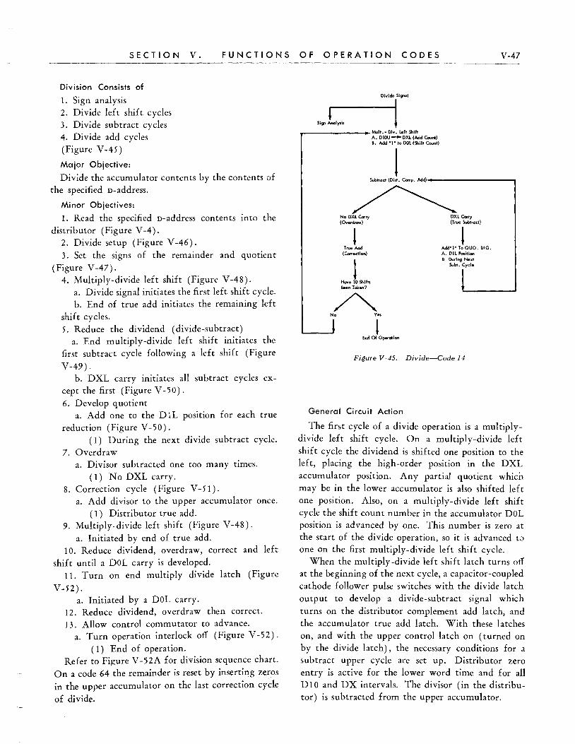
SECTION V. FUNCTIONS OF OPERATION CODES V-47
Division Consists of
1. Sign analysis 2. Divide left shift cycles 3. Divide subtract cycles 4. Divide add cycles (Figure V-45)
Major Objective:
Divide the accumulator contents by the contents of the specified D-address.
Minor Objectives:
1. Read the specified D-address contents into the distributor (Figure V -4).
2. Divide setup (Figure V-46). 3. Set the signs of the remainder and quotient
(Figure V -47). 4. Multiply-divide left shift (Figure V -48).
a. Divide signal initiates the first left shift cycle. b. End of true add initiates the remaining left
shift cycles. 5. Reduce the dividend (divide-subtract)
a. End multiply-divide left shift initiates the first subtract cycle following a left shift (Figure
V-49) . b. DXL carry initiates all subtract cycles ex
cept the first (Figure V-50). 6. Develop quotient
a. Add one to the DIL position for each true reduction (Figure V - 5 0 ) .
(1) During the next divide subtract cyct..:. 7. Overdraw
a. Divisor subtracted one too many times. (1) No DXL carry.
8. Correction cycle (Figure V-51). a. Add divisor to the upper accumulator once.
(1) Distributor true add. 9. Multiply-divide left shift (Figure V-48).
a. Initiated by end of true add. 10. Reduce dividend, overdraw, correct and left
shift until a DOL carry is developed. 11. Turn on end multiply divide latch (Figure
V-52) . a. Initiated by a DOL carry.
12. Reduce dividend, overdraw then correct. 13. Allow control commutator to advance.
a. Turn operation interlock off (Figure V-52).
( 1) End of operation. Refer to Figure V -52A for division sequence chart.
On a code 64 the remainder is reset by inserting zeros in the upper accumulator on the last correction cycle
of divide.
J Sign Analysis
r--_____ .-I.'ult.-Div. Left Shift A. DlOU-DXl (Add Count) B. Add "1- to DOL (Shift Count)
I Subtract (Did. Compo Add)I __ -------...,
~ No DXL Carry DXl Ccny (Ov."j,aw) (T,u. Sub""cI)
l True Add
(Correction)
1 Have 10 Shlfh Been Token?
~ No Yes
~ End Of Operation
l Add"1" To QUO. DiG. A. OlL Position B. During Next
Subt. Cycle
Figure V-45. Divide-Code 14
General Circuit Action
The first cycle of a divide operation is a multiplydivide left shift cycle. On a multiply-divide left shift cycle the dividend is shifted one position to the left, placing the high-order position in the DXL accumulator position. Any partial quotient whicn may be in the lower accumulator is also shifted left one position. Also, on a multiply-divide left shift cycle the shift count number in the accumulator DOL position is advanced by one. This number is zero at the start of the divide operation, so it is advanced to one on the first multiply-divide left shift cycle.
When the multiply-divide left shift latch turns off at the beginning of the next cycle, a capacitor-coupled cathode follower pulse switches with the divide latch output to develop a divide-subtract signal which
turns on the distributor complement add latch, and the accumulator true add latch. With these latches on, and with the upper control latch on (turned on by the divide latch), the necessary conditions for a subtract upper cycle are set up. Distributor zero entry is active for the lower word time and for all DIO and DX intervals. The divisor (in the distributor) is subtracted from the upper accumulator.

A-C
OPQ4UN
Enable Arith Codes Sig
Cf fa. ::-;'\:' 10R ~i~Snift 9 (8-30 AL)
NWPL
Dist. Compl. End
-r -~
o IOU
OP BOUN
Of BOT
Div. Sig
OR
Enable Arith Codes Sig
No Res.t Sig. ~R.,et Sig
OR ¢::em. Ctrl. Latch (8-30 BL)
o Reset Sig.
OR-------I
Reset Sig.
Rem. Check
Divide Latch (8-30 AL)
OR OR
CF Upper Ctrl
OR OR fist.T.A. Latch
Div. Subt. or DIOU
~Ge'T'A'
Latch
NWPL
EDXL
Rem. Sign Reset
To Rem. Plus latch
To Rem Minus Lotch
01
End M.D.On Div. Left Shift
Divide latcn
Figure V -46. Divide Controls
DO
Ace. Minus Sign
Ace. Sign Reset
To Ace. Plus Latch
Figure V-47. Divide Sign Analysis
V-48
OR
AGe. Reg.n.t Latch Cf (8-20 CU) AGe R.I.
End M.D. Lotch End
Rem. Plus Sign
To Ace. Minus Latch
Gatt'!
NEDX
To Ace. Minus latch
Latch (8-31 AU)
End MID Off
To Ace. Plus Latch
Rem. Plus Sign

EDXL
I--------...... ----;:=====:::!._ "0" Insert
Add "I" DXL
EndT.A. ( Initiates Remaining
Left Shift Cycl .. )
"on Insert On Initial l. S. (To Satisfy Validity)
Div. Signal ( Initiates First Left Shift Cycle)
Acc. T.A. At DXL
Increase Shift Count
Number By One
Left Sh 1ft Gate
No-Carry Inserts DXL, DOL, DI L
Quo. Digit Off Div. On
End M.D. Off
L....----_~OR
OR
Any Shift ( 8-30 DU )
Ace. Regen Off
Neg.Sh. Num.Gate
DXL
Arith Operation Latch On
Ace. True Add Gate DXL
CFPM.D. I Lt.Sh.
EDXL
Zero Insert
MuIt.Div.Lt.Sh. Latch ( 8-30 AL )
EDIL
OR
No Camp Ace.
EDL ~EDOL OR
1 No-Corry In •• rt ( 8-30 EU )
Figure V-4B. Divide Left Shift
V-49
Ace. R.I. Gote
S.D. Add "I" @DXL "0" Except DXL
EDXU
BP
Dl
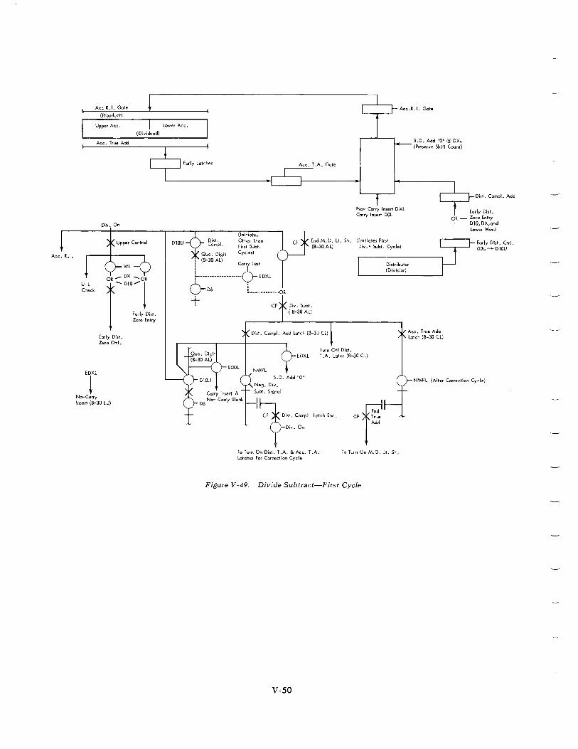
Acc R.I. Gate
(Prouduet)
Upper Ace.
Ace. True Add
Er No-Carry
Dlv. On
Early Dist. Zero Ctrl.
Insert (8-30 EU)
[ Lower Ace.
(Dividend)
I
1 Acc.R.I. Gcte
S.D. Add "O"@DXL ~ (Preserve Shift Count)
I I Early Latches .-_"A.:.,,:..;._T .A. Gate
I I
I (Initiates
t No- Carry Insert DXL Carry Insert DOL
D10U -0- Qist. Other Than Compl. First Subt.
End M.D. Lt. Sh. (Initiates First (8-30 AL) Div .... Subt. Cycle)
)k Quo. Digit Cycles)
: (8-30 ALl Car Test
~------------------.2): EDXL
0- D6 L----------.OR
+
~ Oi". Compl. Lotch End.
TOiV. On
To Turn On Dist. T .A. &. Acc. T .A. Latches For Correction Cycle
Cf E) True Add
Distributor (Divlsior)
To Turn On M.D. Lt. Sh.
Figure V-49. Divide Subtract-First Cycle
V-50
I I Dist. Compl. Add
t Early Dist. OR _ Zero Entry
DIO,DX,and Lower Word
Early Dist. Ctrl. DOU-DIOU
NWPL (After Correction Cycle)

Ace . R.I. Go" fr--------------------------------,
Ace. True Add
L-_,-_..J Early latches Ace. LA . Gate
Distrib~tor
Div. On
No-Corry Inst"rt DXL Carry Ir-s..: rt D II
S.D. Add "0" DXL "I" DOL ( Increase Quotient Digit)
Dis'. CampI. Add
OR ___ Early Dist. Zero Entry
I-- Early Di.,. C'rl. L--,,.------I. OOU _ 0 IOU
;
• 010, OX & WL
1------'
..--------+--------.----,--------------------------------------------. i
Ace. R. I.
U -L Check
EDXL
l No-Corry
..... ox .... OR OR
t~n~:O/ ~ Early Dist . Zero Entry
Early Di. ,. Zero etrl.
EDOL
Insert ( 8-30 EU ) S.D. Add"I" (Adds "I" To Quo. For Each True Reduction Cycle)
Did. Campi . ( From Preceding Subt. Cycle)
: CF~
9--------J
End M/D L,. Sh_
Cor Test
: I EDXL
L-_______ OR
D6 CF
Oi.t. Campi. Add La'ch ( 8-30 CL )
£DXL
y
- EDIL NWFL S.D. Add"O"
Neg. Div .Sub' . Si9 .
Div. Subt . ( 6-30 AL)
Turn Off Dist. T.A. la'ch
COiry Insert & No-Corry Blank
g OJ,,. Campi. la'ch End fnd
CF T"", Add.
Y-DiV. OIl
To Turn On Dlst. LA. & Ace. LA. Latches For Correction Cycle
To Turn On M. D. L,. Sh.
Figure V-50 . Divide Subtract--Except First Cycle
V-51
Ace. True Add La'ch ( 8-30 CL )
NWPL ( After Correction Cyeie )

Ace. R.I. Gab!
Upper Ace.
Aee. True Add
Ace. R.I.
U-L Check
Div. On
Inv.
Early Dist. Zero Orl.
NEDX
Lowe:r Ace.
Early Djst. Zero Entry
Eady latches
To Turn On t-.\ult. Div. Lt. Sh.
Ace. T .A. Gote
No-Carry Insert@ DXL and DOL
Ace. R.I. Gote
Dist. True Add
Early Dist. OR --Zero Entry
Dl0,DXand WL
Early Dist. Ctrf. DOU-ol0U
Distributor
CF
Dist. Compl. Latch End. (8-30 CL)
No Compl. Acc.
EDXL "' D~ L ~ EDOL
OR
I No-Coery Im.,t (8-30 EU)
Figure V-51. Divide Add-Correction Cycle
Arith. Operation Latch (8 - 30DU)
CF
Quo.Dig.Off
End True Add (8- 30CL)
Dlv. Lt. Sh. (8 - 30Al)
1'~"' 0",""_
Turn Operation Intlk. Off
Div ide lateh (8- 30AL)
Dl
End Mult. Div. Latch (8 - 30AL)
? End M.D. U l' Latch End
Turn Ace. Regen. On
Figure V-52. End of Divide
V-52
DOL CQ/7y Latch (8 - 30BU) (During tenth left shift)
NWPL

SECTION V. FUNCTIONS OF OPERATION CODES V-53
On this cycle the high order dividend digit in the DXL accumulator position enters the adder at DIOU time, merges with a complement zero from the distributor zero entry circuit, and comes from the adder at DXL time to enter the DXL accumulator position. It is the carry or no-carry impulse signal frora the adder, during this DXL time, which is tested to determine whether or not the sign of the reduced dividend has changed. The quotient digit latch is turned on at DIOU time of each reduction cycle by testing with a DIOU timing gate to discover whether or not the distributor complement add latch is on. The quotient digit latch output switches with a DXL timing gate and a carry test to test for a sign change.
If a carry is present, a divide subtract signal is developed, which shunts the NWPL reset of the distributor complement add, and accumulator true add latches, thus holding them on for another reduction cycle. If the distributor complement add latch stays on, the quotient digit latch output switchel with distributor complement add and DOL to operate special digit-add one to enter a quotient digit of one during this next reduction cycle.
The quotient digit latch output also controls the carry insert circuit so that a carry is inserted at D I L on all divide complement add cycles except the first
one after a shift, instead of at DoL as on other complement add cycles. This inserts the necessary elusive one into the D2L position when dividing, on all cycles when a quotient entry is made in the Dl L posi tion; but allows its insertion in to the D I L position on the first reduction cycle after a shift, wh!.':1 no quotient entry is made. This is illustrated in the preceding simplified chart of division.
Reduction cycles continue until no DXL carry occurs. No divide subtract signal is developed to shunt the NWPL reset of the distributor complement
add latch. As the distributor complement add latch goes off, on a divide operation, a capacitor-coupled
cathode follower impulse holds the accumulator true add latch on and turns on the distributor true add latch. With accumulator true add and distributor true add on, the necessary gates are developed to true add the distributor to the upper accumulator. thus providing the correction cycle.
At the end of the correction cycle the accumulator true add latch turns off. A capacitor-coupled im
pulse, when it goes off, switches with divide latch
on and quotient digit latch off to develop a divide left shift signal which turns the multiply-divide left latch shift on, if the end multiply-divide latch is still off.
This process of shifting, reducing and correcting and the consequent entry of quotient digits continues until the shift count number in the accumu
lator DOL position is advanced to ten, as indicated by a DOL carry. This carry turns on the end multiplydivide latch. With this latch on, the divide left shift signal at the end of the last correction cycle is prevented from turning on the multiply-divide left shift latch and instead turns off the divide latch to stop the operation.
TABLE LOOKUP
THE terminology used is defined as follows: Argument-Known reference factors. Function-Unknown results associated with the argu-
ments. Table-An arrangement of arguments in an ascend
ing sequence of absolute values and a series of associated functions.
On a TLU operation the contents of the word locations of the address selected table band are successively compared with the contents of the distributor. This is accomplished by allowing the general storage outputs to enter the adder via entry A and the on-time distributor outputs to enter the adder, in tens complement form, via entry B. An adder DX carry indicates that an equal or next higher argument has been found. If no adder DX carry is
detected, the selecting address in the D-address positions (5-8) of the program register and in the address register must be increased by fifty. This is accomplished by running the contents of the program register through the adder during the forty-ninth word interval of the band, adding a five to its D6 position and storing the result back in the program register.
The modified D5 through D8 positions also enter the address register from the program register ontime lines, in the normal manner. The new general storage selection is available from the address register during D5 through D8 of the forty-ninth word interval. The fiftieth word interval allows time for the general storage selection circuits to recover, before
being used.
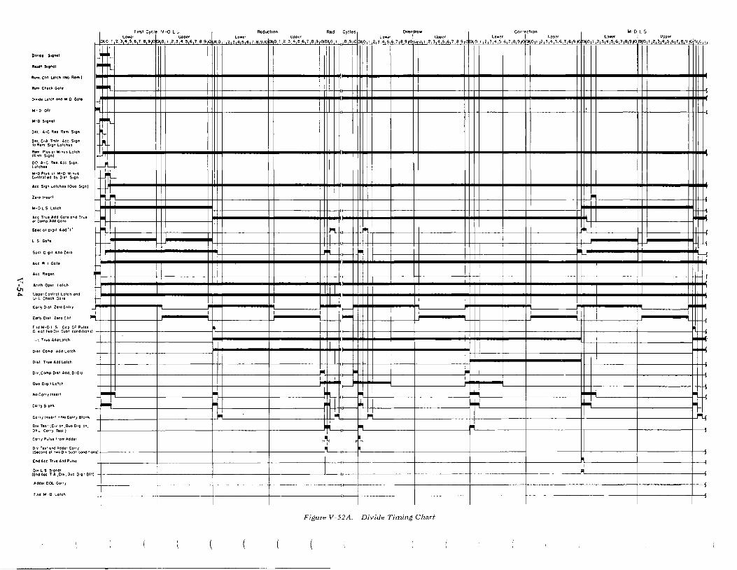
..-: c:" .j>.
OmOe 5'IItOI
Rtstt Si\1nOI
Rem. Clrl L,ottll (No. Rem)
R8m Ctleck Gate
Divide lolCtl GI'Id M 0 Got.
M-O Off
M-O SHilftOI
DXL A-C Res Rem. 510n
OXL C-A T"fr Ace. 51\1" to Rem 5lQn Lote""
ReII'! Plus .or Minus Latch (Rl!m S.gn)
DO A-C Ru. Ace. Sion lotell ••
""-0 Plvs or M-D M,nus v.l<ltroUed by Oisl 5'Qn
Ace 5iQn Latcl'les (Qu.o S";ln)
Zero Innr!
M-OLS Latch
Ate_Tru. Add Goleand True .or Camp. Add Gole
Splc,al O,;il Ada "I"
l S Go!e
5j;lCI 0';11 Add Zero
Acc R I Gote
A\;c Ri;ln
Artlh Oper Loteh
UDpGr Control latch and U- L Check Go I. EOlly 01,1 Zero En!r~
I-
III
"" ht tn
First Cycle rl'1-O L : .. Reduction Red Cycles Overdraw
Upper Lower .. ,., " .• t. Lower ~ Upper
• ' 'H <" "I ii"" " " · , ... ,,',', -~, '1'<,0,<"" ,."~.,, ,',<,0,<,',' ,.,,: CorrectIon I M-D L :::;
Low!!f . I U:-pet L:>'Rer I Upp., . 011,2,3,4,5,6, 7 ,B,)~O~O.I 1213,q.!5IS17!e:91IOjO~OII 12J3j4t5:1G,7jBj9.1O \ll!,OII12_J~413 &~!.I~<j.L.v{C,.ul . .0
00 III 11111 II 111111" IIIIII I II IIII I II IIIII I " I "" II
~
...
I11111 Ii illl I"' ilill Ii ~ Eorly OJ,, Zero GIrl
DIU Comp Add LotCtl ~::,:~:!:~.:"" IIII fll I 111111:: IIIII1 I I' IIII I I' '1111 I' "I 0,., True AddlOlcl'l
DI~ ,Camp 0.,1 Aad, 0 10 U
O~.o O'q,1 Lalcll
N~ Cor.y 'nse"
Corry Blol"Ili
~rr)' 'n,," - No Corry Blonk
D.,. Tul (D,y on,O ... o Oil;! on, DXL Corry T.st)
Carr1 p.,..,. from tldder
~I U I'
I~ ,.. -t:l n I m-++ ..
~ I
fS;t~~$~ ~~~!dg~ ~~;;~cond'I'O"': I ~---H---r II E"d ACt Tr u' Add Pwl,. 1'1
AOder DOL Corr 1 (~:d~ ~.~~o~" ,0" 0 ••• , Off) I ! _ II ': II II ~ t I :
t~-· I ------+--+. ---<::<-+. ---J-i' --I fnd M-O I,..QI,h
Figure V-52A. Divide Timing Chart

Red. Overdraw
J Correction Lower
, '"'r'''T''''''11''' I
M- 0 L S ~correct. on~d Lost M-D L.S Upper Lower Upper M-OL S. Cycles Lower UppGr
2,3,4,5,6,7 ,8,9 ,101~ol I ,2, 314,5J617,BI9Job>;o, I j 2,3 t 4'!)J6 j 7 ,8 19,10 :w;O, I 1.,8,9 t O:W;O, I ,2,3,4,5,15 11'BI91~OII ,2,314,5.6,7,8.9
Re~ Ctrl LQ'Ch INa. Rem)
Rem Chl3CIo, Golt
OJwide LO!Ch Ilr'ld M D Gott
M- 0 Off
RI~ PI\.I" or ","','\I~ LOfth tfhlrn 5'01'1'
I'll
I
I I
", 5°" "" ... to" So,,, !~ i I I Z.rolnHrt i r M~O L S :"f.~eh I I r-r-ACt True Add Gote orld True I I .~~- I
SPtC'OI DIQ" Add "( Ii; I
L 5 Go" I I ,! W-Spc! 01011 Add Z~fO
~ ~ce R I Got~ IJ1 01 \cc. Re'Jar'l
Arllh Ope' ... ol"n I I I I
UpP!H C\".>l'll rot Lole~ ond U-L eMC" ~t"l!
Eorly Dill Zero Enlry
Earl, Dis-I Zaro Clrl
£ftd M-D I... S Cop CF. P\ll~e ,O"eof ''''oD!~ Sub I condlt,ons)
AcC T(\.Ie Add Lotch
Oil! Comp Ajd lotch I I )11.1 Tf\.ll Aod lOICh
)!w,Comp D,!;I Add, DIOU ~T , ..... ".,,. I I ~ 1°
N"o Cerr,lrlSE:r!
:::,::::, .. "".... ; • 0 0,., les! (Ow on,gl.lo 0'9 on,
::':::~:.,," I . ~ (Seeon' " too 0" Subt ''''''''''): EM Act True M<! P\.Ilse
I 01., I. S S"~nQI
(Eod Ace T A ,0,,,, Quo D'Qll Off)
AI1«1. DOL Corry
End M-O Latch
I I
Figure V-S2A. Divide Timing Chart (Continued)
Red. Ond~ Correction cdrwCycle Lower Upper Lower
01,,19 110 [1(,0, 1,2,3,4 15,6 i 7t81911dox..0111213141!:i ,6, 7,8,9 l,dox.OI I ,2,3 ,4,516,718 ,9 Upper
011 !213141!1t617t819
III I: WlJI 4J ~
---+--~~ ~

V-56 IBM 650
Minor Objectives: I. Setup from code 84
A. Table look - up Conlrol Lalch
Single Inllk. Off
"D" Control
DO S4
Table Look - up Control Latch (8 - 3IAU)
Single Inllk. (7 - IOCL)
TLU ~ I '0'" ±
t,·,,·, Figure V-53. Table Lookup Setup--Code 84
The search continues as before until an adder DX carrv is detected. When a DX carry is sensed, a
nu~ber equal to the drum word interval during
which the DX carry was sensed is added to the modified address in the program register. Thus, the general storage address of the equal or next higher argument is found. This addition is done on a program register add cycle, during the word interval following the one on which the DX carry is detected. The value
of the number which is added is determined by the
sector and word timing interval during which the
DX carry is detected. After the desired address is in the program register
an additional cycle is taken, during which the pro
gram register enters the adder, merges with zeros and
the adder output for D5 through D8 is allowed to
enter the lower accumulator.
Major Objectives:
1. Search the table of arguments until one is found that is equal to the search argument; or if there is
no equal, locate the next higher argument.
II. Search the Table of Arguements A. Compare ira the Adder, drum readings and distributor output.
I. Test for OX carry
DX Corry
Adder
Drum
Tobie look-up Control latch (8-31AU)
Hold Adder Reset Control Off (8 - IOAU)
Dl
Carry Insert (8 - 30W)
Selected Storage Add Gate (Drum OutputEntry "A")
Cf
- N(54, WB and W9)
Selected Storage Add (S-31A") (Seacch Gate)
V (6-31)
On Time Disl. Add Gote (Adder Entry "B ")
No-Corry Test -OR-Carry Test
Misc. Error Check Latch (6-31)
DX
A-C
NDO
Figure V-54, Table Lookup Search
Camp-Iement Add
Carry Test latch
NWP
NOTE: The search argument is in the distributor as
the result of a previous operation.
2. Modify the o-address contents of the program
register to indicate the general storage address location of the argument found.
3. Read the modified program register o-address contents into D5-D9 positions of the lower accumulator.
TLU jectives ming is cated.
(Code 84) is complete when these three ob
have been accomplished. Further program
necessary to make use of the argument 10-
Minor Objectives: (Figure V-58)
1. Setup code 84 (Figure V-53) a. Table lookup control latch.
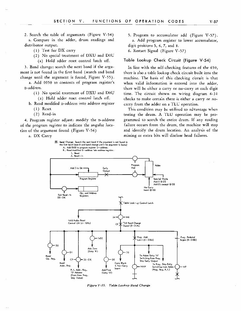
SECTION V. FUNCTIONS OF OPERATION CODES V-57
2. Search the table of arguments (Figure V-54) a. Compare in the adder, drum readings and
distributor output. ( 1) Test for DX carry (2) No special treatment of DXU and DoU
(a) Hold adder reset control latch off.
3. Band change: search the next band if the argument is not found in the first band (search and band change until the argument is found, Figure V-55).
a. Add 0050 to contents of program register's n-address.
(1) No special treatment of DXU and DoU (a) Hold adder reset control latch off.
b. Read modified n-address into address register
(1) Reset (2) Read-in
4. Program register adjust: modify the n-address of the program register to indicate the angular location of the argument found (Figure V-56)
a. DX Carry
5. Program to accumulator add (Figure V-57). a. Add program register to lower accumulator,
digit positions 5, 6, 7, and 8.
6. Restart Signal (Figure V-57)
Table Lookup Check Circuit (Figure V-54)
In line with the self-checking features of the 650,
there is also a table lookup check circuit built into the machine. The basis of this checking circuit is that when valid information is entered into the adder, there will be either a carry or no-carry at each digit time. The circuit shown on wiring diagram 6-31 checks to make certain there is either a carry or nocarry from the adder on a TL U operation.
This condition may be utilized to advantage when testing the drum. A TL U operation may be programmed to search the entire drum. If any reading failure occurs from the drum, the machine will stop and identify the drum location. An analysis of the missing or extra bits will disclose head failures.
m. Band Change: Search. the next band if the argument is not found in the first band (search and band change until the argument is found)
Reset Op. Reg.
A. Add 0500 to program register D-address. B. Read modi fied D - address into address register.
1. Reset 2. Read-in
Add 5 to 06
Program Register
TLU Read -In 05-0X
Hold Adder Reset Control Off (8- iOAU)
01
CP
Reset Addr. Reg.
Add Zero (Entry 18 1)
05- OX
R.I. Addr. Reg. '0 1 Address (From New Prog. Step Value)
ND5
Early Output
Add Five (Entry 'B')
Program Add
Adder
Special Digits Add 5 @05 Add 0', except @ 05
No Carry Insert @DO
Table Look - up Control Latch
54 W8
05
TLU Band Change Signal (8 - 3IAL)
DO
Carry Blank & No-Carry Insert
Prog. Add Latch (8 - 31 BU)
To Adder Entry I A I Switching from Prog. Step Early Output
To Prog. Step Entry NWP Switching from Adder
(Frog. Reg. R.I.)
Figure V-55. TabJe Lookup Band Change
Prog. Pedestal Regen (8-31BU)
WP
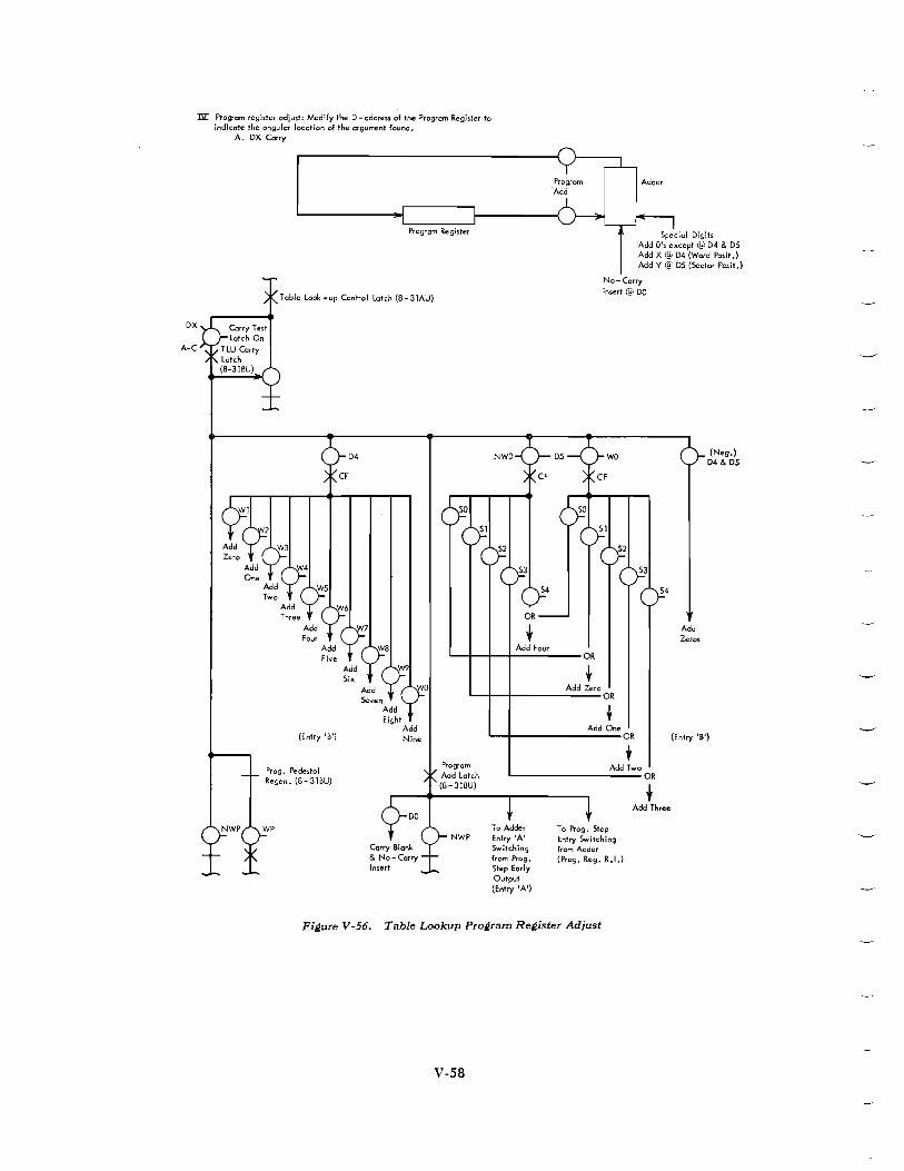
lll' Program register adjust: Modify the 0- address of the Program Register to indicate the angular location of the argument round.
A. OX Carry
Program Register
Table Look - up Control Latch (8 - 31AU)
Special Disih Add 0', except @ 04 & 05 Add X @ 04 (Word Po,it.) Add Y @ OS (Sector Posit.)
No- Corry In,ert@OO
OX
A-C
(Entry '8')
Prog. Pede,tal Regen. (8- 31BU)
OR t
Add Four L--r~--+----------OR
~ Add Zero
L--r~-------------OR
• Add One ~-r---------------OR
t Add Two
~-----------------OR
+ Add Three
Fi~ure V-56. Table Lookup Pro~ram Re~ister Adjust
V-58
Add Zeros
(Neg.) 04& 05
(Entry 'B')
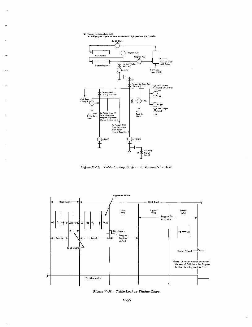
'Y. Program to Accumulator Add. A. Add program register to lCM'er accumulator, digit positions 5,6,7, and 8.
D5-D9 Only
Program Add
Program Register (8-31 BU) ~LUC""Yl.GtCh
Carry Blank & N<>-Carry Insert
Program Add Latch ( 8-31 BU)
To Adder Entry 'A' Switching From Program Step Early Output ( Entry' A' )
NWP
To Program Step Entry Switching From Adder (Prog. Reg. R.I.)
NWP
N<>-Carry Insert @ DOL
1TLuprog. CF Restart
Signal
Figure V-57. Table Lookup Program to Accumulator Add
Argument Address
0500~nd--~~~--------------7--------------------0050~nd----------------------~
Search
lO'Ner W22
Upper. W23. I Lower
W24 .. ____________ Program T ° ___________ ~~
Ace. Add
Program Search ---~~"'---Register
Adjust
"0" Alternation
Figure V-58. Table Lookup Timing Chart
V-59
,,,'" ;; .. , I Note: A restart cannot occur unti I
the end of TLU since the Program Register is be ing used for TlU.
I


SECTION VI. MANUAL OPERATION
MANUAL READ-OUT STORAGE OPERA nON
MANUAL read-out storage is provided to allow the contents of any general storage location to be dis
played. This is accomplished from the control con
sole, as explained in the manual of operation by the
following steps:
1. Stop the program. 2. Set the control switch to MANUAL.
3. Set the display switch to READ-OUT STORAGE.
4. Set the address of the location whose contents are to be displayed in the address selection switches.
5. Depress the program reset key (address register
reset to blanks) . 6. Transfer the address from the address selection
switches to the address register by depressing the
transfer key. 7. Depress the program start key. The control commutator functions in such a way
that when the specified general storage location is selected, its contents are transferred to the distributor and displayed from there. The control commutator
actually functions in rather special ways in accom
plishing both manual read-out storage and manual read-in storage operations.
Major Objective:
Display the contents of a specified general storage location.
Minor Objectives: (Figure VI-l)
1. Find the drum location.
2. Read the contents of the drum location into
the distributor.
3. Restart a. Reset operation and address registers.
4. Turn run latch off.
MANUAL READ-IN STORAGE OPERATION
MANUAL read-in storage is provided to allow the
insertion of any desired numeric word into any
VI-l
general storage location. This is accomplished from
the control console, as explained in the manual of operation by the following steps:
1. Stop the program.
2. Set the control switch to MANUAL.
3. Set the display switch to READ-IN STORAGE.
4. Set the word to be entered in the storage entry switches.
5. Set the address of the general storage location where the word is to be entered in the address selection. switches.
6. Depress program reset key.
7. Transfer the address from the address selection
switches to the address register by depressing the transfer key.
8. Depress program start key.
The control commutator functions to transfer the contents of the storage entry switches to the distrib
utor and then further transfer the contents of the distributor to the specified general storage location.
The contents of the distributor are displayed. The
entire operation is similar to a store code (20's) ex
cept that the word to be stored is taken from the storage entry switches.
Major Objective:
Transfer the contents of the storage entry switches
to the specified general storage location.
Minor Objectives: (Figure VI-2)
1. Transfer the contents of the storage entry switches to the distributor.
a. Heat 8000
( I) Allows the contents of the storage entry switches to appear on the selected storage data flow path.
b. Read-in distributor. 2. Find the drum location.
3. Read-in general storage. 4. Restart
a. Reset operation and address registers. 5. Turn run latch off.

er 0027 Trans! Ta Ad dr. Reg.
Program Start S ..... itch No.2 Key released (WO 7-01e)
~
Obiectives: (WD7 - IO)
I. Find Drum location 2. R.I. Dht
1. Control Switch Manual (WD7-01) 2. Disploy SW R.O. Stor. (WDS-ll) 3. locotion to R.O. in Store Sel. Sw.
(W07-01) '*. Computer Reset S. Transfer (WD7-0l)
3. Turn OFF Run latch and Restart 6. Program Start (WD7-0l)
0024 0025
I 0026 0027
I Program Start Switch I
Run latch
I jOld early
Enable R.I.
Start R.l.
-----.J~ Dist. display in lights
.d
.--J - -
- ~.BSgi ves Restart
WPU
Control S ..... itch on Manual (7 -OIC)
Run latch (7 - 10Al) Display Switch on Read-out Storage (5-IIB) .
CF
OR
MGnual Read- Out S'"oge (7 - JOAL)
Code 69 OR
CF load Did. (7-2ICU)
DX
Read-In CF Dist. Sig.
(7-IOCU)
Dist. Regen. Control (6- IOCU)
010
R.I.Dist. from Storage
DP
Invalid Address Intlk. (Storage Check latch Off 7 - OOAU)
Dist. Bock Signal latch (7-IOBL)
Fi~ure VI-I. Manual Read-Out Storage
VI-2
OR
1DbI.lnv.
CF
Enable Re~-ln (7-IOIJU)

Progrom Start Switch No.2 Key released (WD7-0IC)
, Transfer 0125 to Addr. Reg.
~
Objectives: (WD7-10)
1. R.I. Dist. from Switches 2. Find Drum location 3. RIGS 4. Restart
0122 0123
Run latch ON
Enable R.I.
R.I. Dist. Signal
~ R.!. Oist.
Program Start Switch No.1
Error Stop Lotch Off
CF
CF
Run Latch (7 - WAL)
WPU
CF N\anual Read - In Storage (7 - lOAl)
010
D9
Start ReadIn (7 - 10BU)
Setup
1. Control Switch Manual (WD7-0l) 2. Display Switch R.1. Storage (WD5-11) 3. location to R.I. in Address Selection
Switches (WD7-0J) 4. Computer Reset (WD7 - 02) 5. Transfer (WD7-0l) 6. Program Start (W07-0l)
0124 0125
~ Manual R.I. Star.
I 1 Word. Early
Control Switch on tliLonuol (7- OIC)
NEDI
Display Sw itch on Reoo - In Storage (5 - II B)
OJ,t. Bock Sig. Lotch (7 - 10BL)
Restart Signal
Dist. Reger,.
16-IOCU)
~p
010
I to 0125
I End RIGS
Reao - In Dist. from Stor.(6-lOCJ)
""onua I Stort R.I. Dist. Lotch 17 - 10BU)
Heat 8000 for R.1. Storage
NWP
NAP
Figure VI-2. Manual Read-In Storage
VI-3

SECTION VII. INPUT
THE 655 power unit contains circuits which serve two main purposes.
1. The conversion of card information into the proper information gates for input to read-buffer
storage and the conversion of punch-buffer storage information gates into a form suitable for punching.
2. Main power supply for the 650 machine.
CONVERSION CIRCUITS FOR READ-IN AND PUNCH OUT
CHASSIS 13 and 14 in the 655 contain much of the circuitry used in transferring information between cards and drum storage.
Refer to Dru III Arrangement section for general information on buffer storage functions.
Read-In from Card (Code 70) (Figures VII-l to VII-5) General Circuit Action
Ten words of information may enter RBS on each read operation. These ten words can then be transferred to the word one through word ten locations of any general storage band on a subsequent read operation. Figure VII-IA shows the time during which the digits of these ten words must be available from general storage. To be available from general storage ontime (as shown in Figure VII-IA), information must have been presented to general storage during a time interval one digit early (Figure VII-IB). Thus, the successive B-A information gates, representing the ten words of information in RBS, must be available from the RBS output latches one digit early and must be gated through to the general storage input lines by a ten-word gate, which is one digit early.
In order for information to be available from the buffer storage output latches one digit early it must be presented to the buffer storage record circuits two digits early, during the time shown in Figure VII-ID.
Because of the length of the lines and intervening units, information gates are delayed considerably between the output of the scan circuits and the input to buffer storage. To insure that information will be two digits early at buffer storage input, it is scanned
VII-l
AND OUTPUT CODES
from the card three digits early. The delay is then controlled by the scan delay latch with the result that two-digit-early information gates, which nicely overlap the write sample pulses, arrive at the buffer-storage record circuits. This delay action is shown in Figure VII-I.
The information gates from the read scan circuits are controlled by the output of the RBS timer so that they can reach the buffer-storage input only during the two-digit early, ten-word interval associated with RBS. The RBS timer establishes the basic RBS timer interval. Its output is also used by the buffer-storage transfer and erase control circuits in the development of the RBS to GS transfer gate and the BS erase gate for erasure of RBS. Its output is shown in Figure VII-IF.
The output of the read scan circuitry is a series of three-digit-early, B-A, digit gates. Each of these gates is produced by its own cathode follower, which serves to associate a specific card column with a specific digit position of drum storage. Note that the cathode follower has anode voltage applied by action of a brush reading a hole in the card. When one of these gates occurs during the time that the RBS timer is on, it turns on the scan delay latch whose output is a D-C gate (approximately 2 Yz digits early).
The presence of one of these scan delay gates is an indication that a digit is to be recorded in RBS in the digit and word position represented by the time of occurrence of the gate. The numerical value of the
digit to be recorded is established by the reader CB time during which the gate occurs. The single D-C scan delay gate is converted to two of seven bi-quinary form by the bi-quinary cathode followers. Anode voltage is applied to these cathode followers by emitters synchronized with the read feed. Thus, at zero CB time only bi-quinary zeros can be generated, and so on.
As a result of this circuit action on read feed cycles, two and one-half digit early bi-quinary information gates are sent to buffer storage during each successive digit interval included in the RBS timer gate. Zeros are entered on one drum revolution during zero CB time, ones on a later revolution during one CB time,

7 Time C.B. Impulse Duration 5.8 ms.
Digits Entered From Cord Must A Be Available From G.S. During
C
D
This Time
Digits Must Enter G.S. From RB During This Time (One Digit Early)
RBS to GS Transfer Gate
Digits From Read Sccn Circuits Must Be Available During This Time For Entry to RBS (Two Digits Early)
Digits Scanned From Cord During This Time (Three Digits Early)
RBS Timer, Gotes RBS Read-In And Ero~ure
S
Typical Digit Scan Gate. Inpu To Read Scan Matrix (Digit
t
Ten Scanning Of WI Is Shown
DP
NCP
Digits Delay Latch
Delayed Gate From Sccn Delay Output As I t Appears At RBS Input (Two Digih Early)
WSP For Record In RBS
B - A Information Gate from RBS to GS Input (One Digit Eady)
)
7 Hole In Cord WI
Sector 0 \ --------- Sector
WO WI W2
OXOOOI 02030405DE07 DB,or: OX DC O'ID2 03 D4,051
06 07·D8 091D<:
I I I
I I
--Wo----~>+I·~-----~
ox IDO 0 I 102,03 0405060708,09 pc OX ,DC 0'
f--!-. I
I
I " I / III
I I I
I I I
J
Lasts One Digit Longer Than Necessary
I I~.
J~
.~
I
I I ~
I I
~ I I
5 - 9 CB's
RBS Timer
B5 85
BFR Z ... ~
02 02
2& 7C.B. One One WI Digit Digit DIO Delay Delay
On Time
Figure VII-I. Card-to-General Storage: Read "7" Hole to WI, DIO
VII-2
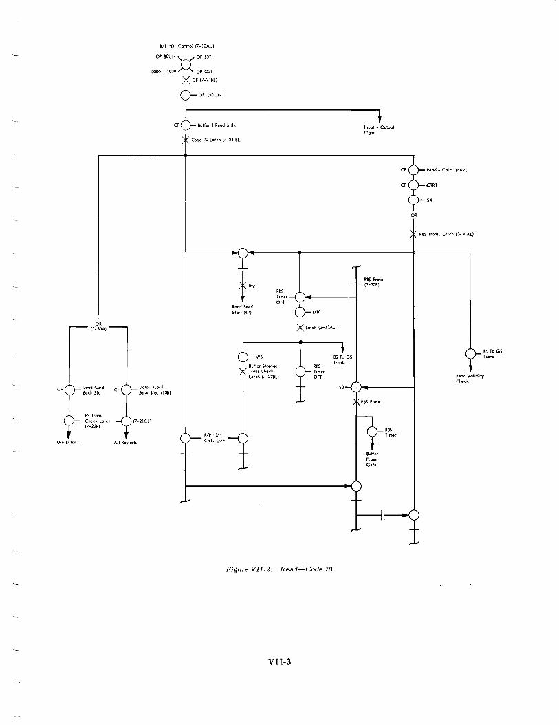
CF
Use 0 for I
OR (3~30")
Load Cord Back Sig.
BS Trons. Checlc Latch (7-228)
All Restarts
I!/P "D" C.nt •• 1 (7-IO"U)
OP 80UN
0000 - 1999
OP QOUN
Buffer 1 Read '"tile
Detail Card Bo,k 5;9. (138)
I!/P "D" etrl. OFF
Read Feed Start (R7)
W6
RBS Timer ON
Buffer Storage Trans Check Latd. (7-228L)
FiAure VJl-2. Read-Code 70
VII·3
Input - Output Light
RBS Erase (3-308)
RBS Erase
Buffer E .... Go ..
R85 Timer
CF
CF
OR
Reod - Colc. Intlle.
eRRl
54
RBS Trans. Latch (3-30AL),
IS To G5 Trans
Read Validity Ched<
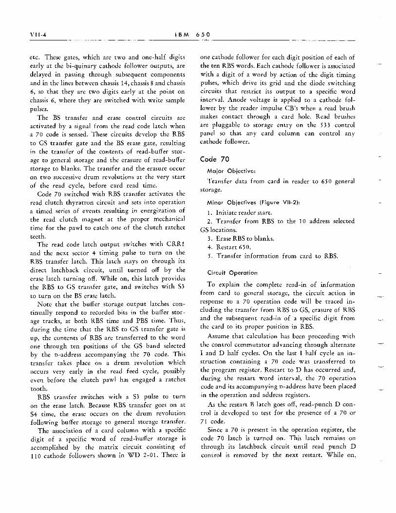
VII-4 IBM 650
etc. These gates, which are two and one-half digits early at the bi-quinary cathode follower outputs, are delayed in passing through subsequent components and in the lines between chassis 14, chassis 8 and chassis 6, so that they are two digits early at the point on chassis 6, where they are switched with write sample pulses.
The BS transfer and erase control circuits are activated by a signal from the read code latch when a 70 code is sensed. These circuits develop the RBS to GS transfer gate and the BS erase gate, resulting in the transfer of the contents of read-buffer storage to general storage and the erasure of read-buffer storage to blanks. The transfer and the erasure occur on two successive drum revolutions at the very start of the read cycle, before card read time.
Code 70 switched with RBS transfer activates the read clutch thyratron circuit and sets into operation a timed series of events resulting in energization of the read clutch magnet at the proper mechanical time for the pawl to catch one of the clutch ratchet
teeth. The read code latch output switches with CRR1
and the next sector 4 timing pulse to turn on the RBS transfer latch. This latch stays on through its
direct latchback circuit, until turned off by the erase latch turning off. While on, this latch provides the RBS to GS transfer gate, and switches with S3
to turn on the BS erase latch. Note that the buffer storage output latches con
tinually respond to recorded bits in the buffer storage tracks, at both RBS time and PBS time. Thus, during the time that the RBS to GS transfer gate is up, the contents of RBS are transferred to the word one through ten positions of the GS band selected by the D-address accompanying the 70 code. This transfer takes place on a drum revolution which occurs very early in the read feed cycle, possibly even before the clutch pawl has engaged a ratchet
tooth. RBS transfer switches with a S3 pulse to turn
on the erase latch. Because RBS transfer goes on at S4 time, the erase occurs on the drum revolution following buffer storage to general storage transfer.
The association of a card column with a specific digit of a specific word of read-buffer storage is accomplished by the matrix circuit consisting of 110 cathode followers shown in WD 2-01. The~e is
one cathode follower for each digit position of each of the ten RBS words. Each cathode follower is associated with a digit of a word by action of the digit timing pulses, which drive its grid and the diode switching circuits that restrict its output to a specific word interval. Anode voltage is applied to a cathode follower by the reader impulse CB's when a read brush makes contact through a card hole. Read brushes are pluggable to storage entry on the 533 control panel so that any card column can control any cathode follower.
Code 70
Major Objective:
Transfer data from card in reader to 650 general storage.
Minor Objectives (Figure VII-2):
1. Initiate reader start. 2 . Transfer from RBS to the 10 address selected
GS locations. 3. Erase RBS to blanks. 4. Restart 650.
5. Transfer information from card to RBS.
Circuit Operation
To explain the complete read-in of information from card to general storage, the circuit action in response to a 70 operation code will be traced including the transfer from RBS to GS, erasure of RBS and the subsequent read-in of a specific digit from the card to its proper position in RBS.
Assume that calculation has been proceeding with the control commutator advancing through alternate I and D half cycles. On the last I half cycle an instruction containing a 70 code was transferred to the program register. Restart to D has occurred and, during the restart word interval, the 70 operation code and its accompanying D-address have been placed in the operation and address registers.
As the restart B latch goes off, read-punch D control is developed to test for the presence of a 70 or 71 code.
Since a 70 is present in the operation register, the code 70 latch is turned on. This latch remains on through its latchback circuit until read punch D control is removed by the next restart. While on,

<: H H
&,
Back Signal y Control .~. _
-wDM1----- ---N;---r--
7P
~~I~ ~ ~I o 0:2 0
too ~
• I
I I I I I I I I
~
~I t .gl .:
-150
.~ b~ M240 R46
B 295 CRRI P M 2420
~~ O.k. f M "" r='~ B 3100
Interlock B 250 0 152-3
9-2
100
14L9
R":"I_ --1'" PC 12 14Pb -. -------- RC4 --132 ,'fI, RC 131
61~ &ti~
~O
N .... -8 .s
Figure VlI-3. Read Feed Circuits
;;!;
.. ISO Source
-70
[1p R47 M'199°
'T" B 294°
I til"'" Read Clutch
RP 14
RP2-2
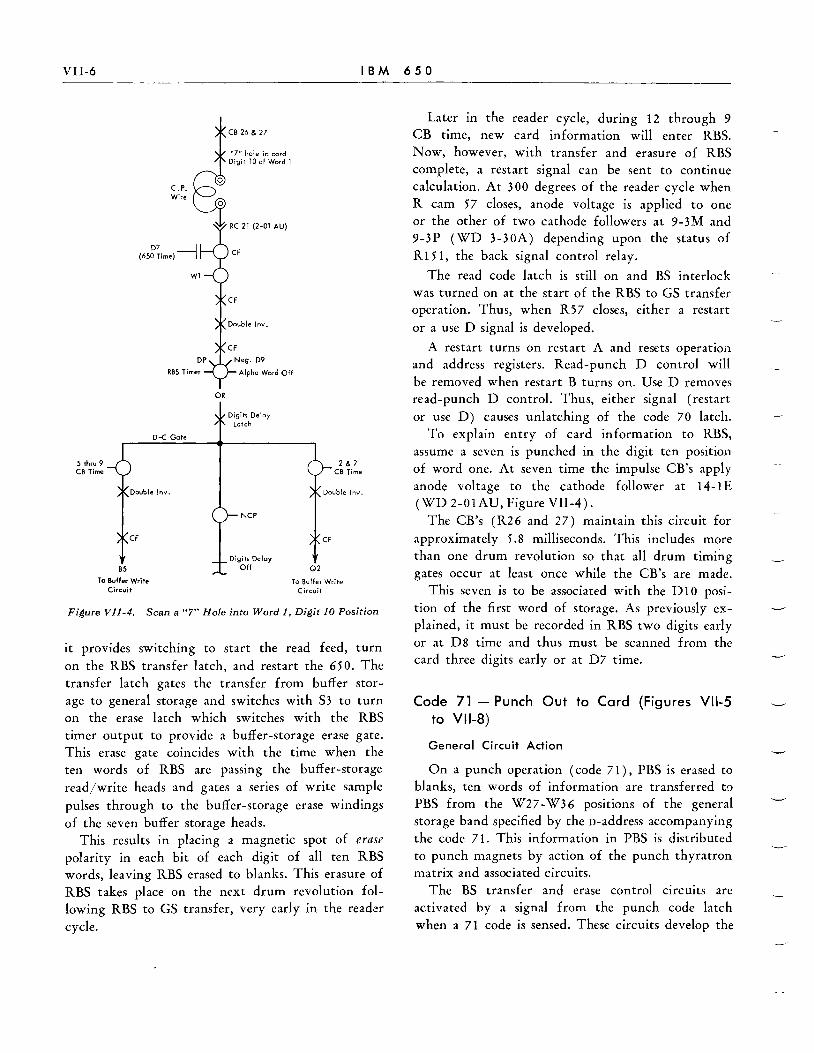
VII-6 IBM 650
5 the" 9 CB Time
B5 To Buffer Write
Circuit
C.P. Wire
OR
Alpha Woed Off
Digits Delo), Latch
NCP
Digits Delay Off
CF
Q2
2 & 7 CB Time
To Buffer Write Circuit
Figure V/l-4. Scan a "7" Hole into Word 1, Digit 10 Position
it provides switching to start the read feed, turn on the RBS transfer latch, and restart the 650. The transfer latch gates the transfer from buffer storage to general storage and switches with S3 to turn on the erase latch which switches with the RBS timer output to provide a buffer-storage erase gate. This erase gate coincides with the time when the ten words of RBS are passing the buffer-storage read/write heads and gates a series of write sample pulses through to the buffer-storage erase windings of the seven buffer storage heads.
This results in placing a magnetic spot of erase polarity in each bit of each digit of all ten RBS words, leaving RBS erased to blanks. This erasure of RBS takes place on the next drum revolution following RBS to GS transfer, very early in the reader cycle.
Later in the reader cycle, during 12 through 9 CB time, new card information will enter RBS. Now, however, with transfer and erasure of RBS complete, a restart signal can be sent to continue calculation. At 300 degrees of the reader cycle when R cam 57 closes, anode voltage is applied to one or the other of two cathode followers at 9-3M and 9-3P (WD 3-30A) depending upon the status of R 151, the back signal control relay.
The read code latch is still on and BS interlock was turned on at the start of the RBS to GS transfer operation. Thus, when R57 closes, either a restart or a use D signal is developed.
A restart turns on restart A and resets operation and address registers. Read-punch D control will be removed when restart B turns on. Use D removes read-punch D control. Thus, either signal (restart or use D) causes unlatching of the code 70 latch.
To explain entry of card information to RBS, assume a seven is punched in the digit ten position of word one. At seven time the impulse CB's apply anode voltage to the cathode follower at 14-1 E (WD 2-01AU, Figure VII-4).
The CB's (R26 and 27) maintain this circuit for approximately 5.8 milliseconds. This includes more than one drum revolution so that all drum timing gates occur at least once while the CB's are made.
This seven is to be associated with the D 1 0 position of the first word of storage. As previously explained, it must be recorded in RBS two digits early or at D8 time and thus must be scanned from the card three digits early or at D7 time.
Code 71 - Punch Out to Card (Figures VII-5 to VII-8)
General Circuit Action
On a punch operation (code 71), PBS is erased to blanks, ten words of information are transferred t'J
PBS from the W27-W36 positions of the general storage band specified by the D-address accompanying the code 71. This information in PBS is distributed to punch magnets by action of the punch thyratron matrix and associated circuits.
The BS transfer and erase control circuits are activated by a signal from the punch code latch when a 71 code is sensed. These circuits develop the
Card Flead T. m.
Read Cam I nllk (R30)
Read Clulch Canlrol (R226-12 a R 17-12 R Cam 0)
Read Com Back S.gnol (R31)
Fleod Code Lolch
Advance Read Feed Lolch
288 324
3 6 342
I-..... -~ •• '05_,"1
~~,--+-I' ---H
~~ I "--t--I--i
360 IS
36 54
72 'Or8 '44 'iSO 2'6 90 126 162 198, 252
234 270
288
'iII_._~_~:~Cdh;~gnol Sensed Feed
.. ~~i~~+-~i~~~~+-~ I :
R Cam II Thyrolron Anode _oi'0 Voltage and Relay 7 r--I"
24::.' ... -I_II( ___ Thyrotron Anode Voltage • applied wilh Feed Lolched
CRR Com
R Com 33-ReodClulch Circuit
Card Punch Time
R 162
P 27 Punch Clulch Conlrol
• ~or
o
14
l-
• • • •
I I RBS 10 G 5 Transfer and I--Erase has unlil Bock Signal I Com makes here, to be completed ,
12 0 2 X ,
~ , ~ ~
'" P 30 Punch Bock Signal I .6~ ~4.1
•
Punch Code Lolch
Advonce Punch Feed Lolch
P 16 Thyrolron Anode Voltage and Relay 166
CRP-I Picks RI60 Slarl Rela
P 14 R 160 Hold
CRP-2 Picks P Clulch
PI P Clulch Circuli
,
~ f----1 -l f----1 13.55
• • • • - •
- - - I- ~ --I PBS Erose and Transfer !-has unl" Bock S'9nol Cam I makes here, to be completed. ,
• •
4 3
• ~
• • -- ~
5
~
• • Thyralron fires. Feed slil\ ·-Iolched. R7picks 2451'0
ril' "'~_"'''''_I\--CluICh energized I 'I
R B S 10 G, S Transfer ' slorls here when Read---l Code Lalch comes on , ,
,
6 8 7 9
:. .- ~ ~
'3
u
~~
rr-...
1--; Punch Si9nal sensed
Thyrolron Anode Voltage applied
• • • • Thyratron fire.
~
9.2 9j. .. --~ r.; PBS Erose .Iorls here when Punch Code Lolch ~ comes on I ,
,
R 166 picks
I-Clulch eneroiud
Figure VII-So Read-and-Punch Feed Timing Charts
VIJ-7

VII-S IBM 650
RIP "0" Control (7-lOAU)
Code 71 lotch (7-2IBL)
Input - Output light
Buffer 1 PBS Intlk (3-30q
CF Punch-Calc. Irltlk
CF
All Restart
Punch Back Si9.
as TroFU
Check Latch
RIP "0" Ctrl. OFF
PBS Intlk
Punch Feed Stort, RIM (p-calT1s etrl. punch validity check.)
\1
\0
Buffer 1 PBS Tran~.
\4
GS To BS Tran$
Buffer I PBS Timer
W6
RIP "0" etrl. OFF
Erose Gate
Buffer I PBS Timet
Figure VIl-6. Punch-Code 71
BS erase gate and the RIPBS gate, resulting in the erasure of PBS to blanks and the transfer of the contents of W27 -W3 6 of the selected general storage band to PBS. The erasure and the transfer occur on two successive drum revolutions at the start of the punch cycle, before card punching time.
The association of a specific digit of a specific word of PBS with a card column is accomplished by the matrix of 110 thyratrons shown in WD 2-13. There is one thyratron for each digit position of each of the ten PBS words. Each thyratron is associated with a digit of a word by action of the digit and word timing gates which control its grids.
The PBS timer develops a gate from S2, W7, DO to S3, W7, DO. This is the timed source of the RIPBS gate which allows on-time information from general storage to enter PBS. The PBS timer output also controls the time of development of the BS era~e
gate for PBS.
Major Objective:
Transfer data from 650 to a card III the punch. Minor Objectives (Figure VII-6):
1. Erase PBS to blanks. 2. Initiate punch feed start. 3. Transfer from the 10 address selected GS loca
tions to PBS.

SECTION V I 1. INPUT OUTPUT CO D ES VII-9 ----"-
+150V +70 V
'" 1 J Punch P 24 P 25
M 9 50 Feed M 9"6 M9A B 13 55 B 13.95 B 13.95 B 14.35
533
i i Punch CRP 2 CClle.
161-1 161-3 Intlk
PC 156 PC 16 ---- ------ CRP 1 R 160-4
166
Start Punch Punch Clutch Feed
14 Ph ---1- - - ------- ----- - --- - -PC-3
14 Pc
9 Ny
TH
•
Cod. 70's
'ND 7-21 Bl
Figure VIJ-7. Punch Feed Circuit Composite
4. Restart 650.
5. Transfer information from PBS to card.
See WDO-99 for data flow.
Circuit Operation
To explain the complete punch-out of information
from general storage to card, the circuit action in
response to a 71 operation code will be traced including erasure of PBS, transfer from general storage to PBS and the subsequent distribution of prop
erly timed information impulses to punch magnets.
We will assume that calculation has been proceed
ing, with the control commutator advancing through
alternate I and D half cycles. On the last I half cycle
an instruction contammg a 71 code was transferred to the program register. Restart to D has occurred
and, during the restart word interval, the 71 operation code and its accompanying D-address have been
placed in die operation and address registers.
As the restart B latch goes off, read-punch D control is developed to test for the presence of a 70
or 71 code. Because a 71 is present in the operation register, the code 71 latch is turned on. This latch
remains on through its latchback circuit until read
punch D control is removed by the next restart.
The code 71 latch output switches with buffer
storage interlock latch off output and the next Sl timing pulse to turn on the PBS erase latch.

VII-lO IBM 650
This latch stays on through its direct latchback circuit until turned off at the next So timing pulse, when PBS transfer latch turns on. \Vhile on, this latch provides the PBS erase gate and mixes to turn on the buffer-storage interlock latch.
The PBS interlock latch activates the punch clutch
thyratron circuit and starts a timed series of events re
sulting in energization of the punch clutch magnet at the proper mechanical time for the pawl to catch one of the clutch ratchet teeth. The code 71 latch output
switches with buffer-storage interlock latch off output and the next SI timing pulse to turn on the
PBS erase latch.
The PBS erase latch switches with the PBS timer output to provide a buffer-storage erase gate. This erase gate coincides with the time when the ten words of PBS are passing the buffer-storage readwrite heads and gates a series of write sample
pulses through to the buffer-storage erase windings
of the seven buffer-storage heads. This places a magnetic spot of erase polarity in each bit of each digit of the ten PBS words and leaves PBS erased to blanks. The PBS interlock latch allows the bufferstorage erase gate to be developed only once for any code 71 operation. This erasure of PBS occurs
early in the punch cycle, possibly even before the clutch pawl has engaged a ratchet tooth.
The PBS transfer latch is turned on at so, and
stays on through a direct latch back circuit until turned off by the next S4 pulse. While on, it provides the general storage to buffer-storage transfer gate, which switches with the PBS timer output to
provide the general storage to PBS transfer gate. This gate allows information from general storage
(5 to 7) to enter buffer storage. The PBS interlock latch allows the GS to PBS transfer gate to be
developed only once for any code 71 operation.
Note that the entire contents of the selected band of general storage have been available from the 5 -to-7 circuits ever since the D-address entered the address register. The GS to PBS transfer gate allows only the information in W27 -W3 6 to enter PBS. This transfer from general storage to punch buffer storage occurs on the next drum revolution after erasure of PBS, very early in the punch cycle.
Later in the punch cycle, during 12 through <)
CB time, the transferred information now in PBS will be distributed to punch magnets for entry into
the card. Now, however, with erasure and transfer to PBS complete, a restart signal can be sent to continue calculation. At 13.65 on the punch index,
when P cam 45 closes, anode voltage is applied to the cathode follower at 14- 5M and a 650 restart is developed.
This turns on restart A and resets the operation and address registers. Read-punch D control will be removed when restart B turns on. With read-punch D control removed, the code 71 latch will unlatch. Removal of the code 71 latch output also inter
rupts the latchback path of the PBS interlock latch, allowing it to turn off.
Bi-quinary information gates from the bufferstorage output latches are continuously applied to the grids of the bi-quinary cathode followers (WD 2-12AU). Anode voltage is applied to these cathode followers by emitters synchronized with the punch, with the result that the cathode followers respond only to bi-quinary zeros during zero CB time, ones during one time, etc.
The output of the cathode followers is switched to provide a single information gate at a digit and
word time indicative of its position in PBS. This gate enters the thyratron matrix and because of its time of occurrence is able to energize only one thyratron. This thyratron associates the gate with a specific card column.
Note that one-digit-late timing pulses are used
to drive the grids of the thyratrons in the matrix, the sign thyratrons being driven with a D1 gate, Dl thyratrons with a D2 gate, etc. This is necessary because the information in PBS is available for dis
tribution one digit late.
To explain distribution of PBS information to
the proper card column, assume that a seven is stored in the D 1 ° position of the eighth word of PBS. This information will be available from the buffer storage B5 and Q2 output latches at DX time of a W5 timing interval (one digit late). At seven CB time anode voltage is applied to the B5 and Q2 cathode followers by the punch emitters and P44.
Anode voltage is applied to all thyratrons by P2 5, P27, and P28 for about 5.35 teeth on the punch in
dex. P29 and the RC circuitry are for arc suppression and may effectively extend the conducting time of the thyratrons from approximately 1 to 4 milli·seconds depending on the number of thyratrons con
ducting.

SECTION VII. INPUT OUTPUT CODES '"11-11
5 thru 9 CB Time
2&7 C& Time
CF B5 (2-12 AU) CF
CF
R894 -3 8. 4 (2-13 DL)
'f PC 121 @ (533 WiD 7B)
Storage Exit W8 DIO
Neg 0 I Alpha Control Off
NAP PBS Timer
W5
OX (2-13 AU)
Thy (2-13 Al)
!mpuhe CB Open~ (Hold u5ed only with
407 & 537 )
Q2
Figure VII-8. Punch "7'" in W8, DIG from General Storage W34. DlO
To Punch
While this anode voltage is applied during the PBS timer interval, the B5 and Q2 cathode followers respond to the information from buffer storage and the output is a B-A gate during the W5 timing interval included in the PBS timer gate. This B-A gate switches with a DX timing gate and the resulting DX B-A gate drives the first grids of the thyratrons in the
D 1 0 column of the matrix. Only the thyratron in the W8 row will fire because it is the only one whose second grid is driven by :l W 5 timing gate. The relay wired to the thyratron (R894) will be energized until P28 breaks the thyratron anode circuit.
Notice that for each cycle point anode voltage is applied for about 5.35 teeth or at 100 cpm approximately 23 milliseconds. In this length of time the drum revolves about fiyc times, and a thyratron
has several chances to fire.
SIGN READ-IN AND PUNCH-OUT
I r-.; the 650 drum storage system plus signs arc stored as nines, while minus signs are stored as eights. Thus, if a plus word is read into general storage a nine must be entered in the sign storage position (DO). If a minus word is read-in, an eight must be entered in the DO position of the storage location. As with other information, if these DO nines or eights are to be available from general storage at DO time, they must be entered into RBS two digits early or at D 1 0 time and scanned from the card three digits early or at D9 time.
\'«hen information is entered from non-load cards in the 650, the operator has a choice of using either a twelve punch for plus and an X for minus or blank for plus and X for minus. With either choice, the sign can be punched over the units position or in a separate column. Where information is entered from
load cards, a plus sign must be identified by a twelve ;\I1d a minus sign by an X and the sign indication must be punched over the units position.
Sign Read-In (Figure VII-9)
The following list summarizes the vanous W;\ys of handling sign entry.
Load Cards. Load hub wired. Plus. Twelve punch over units position. Minus. x-punch over units position.
No brush to storage entry wiring. Read plus not wired. Read sign over units 110t wired. Read plus relays 30 and 33 are picked with
load relays (533 WD 27 A). Non-Load Cards. Storage entry must be wired
from brushes. A. Plus twelve, Minus x-over units, read plus
wired. Read sign over units wired. Storage entry sign 110t wired from brushes.
B. Plus twelve, minus x-not over units.
Read + wired. RSU 110t wired. Storage entry sign wired from brushes.
C. Plus blank, minus x-over units.
R + 110t wired. RSU wired.
Storage entry sign !lot wired from brushes.

VII-12 IBM 650
.~-.. -Sign over units Sign not over units Minus sign over units Minus sign not over units R+ wired (R30 & 33) R+ w I red (R30 & 33) No plus sign punching No plus sign punching RSU wired (R27) RSU not wired R+ not wired R+ not wired
Load Card W8 sign entry not W8 sign entry wired RSU wired (R27)
~/ RSU not wired
wired W8 sign entry not wired W8 sign entry wired
12 Punch 12 or 11 Punch 12 or 11 Punch 11 Punch II Punch
R88-12 N/O RSS-12 N/C C.P.Wire
RS8-12 N/C C.P. Wire
R91-1 N/O C.P. Wire R266-S N/C
C.P. Wire R266-S N/C
R91-2 N/O R139-9 N/C R263-S N/C
R139-9 N/C R263-S N/C
R20-8 N/O RI36-9 N/C R136-9 N/C No Sign
0 R27-S N/C 0 Punch R27-S N/C
M M
R33-3 N/O R91-1 N/C u R91-2 N/C Jl
'* R91-1 N/C "9" R cam 25 R91-2 N/C
R27-S N/O 0 R20-S N/O 0 R27-S N/O R44-3 N/C R20-8 N/O
R91-2 N/C ;; ;;
R91-2 N/C R33-3 N/C M R33-3 N/O M R33-4 N/C M M <0 <0
R20-S N/O R20-S N/O R23-S N/O
R33-3 N/O R33-3 N/C Pick 44
-----R23-8 N/O
"8" R cam 24
PIck R44 R44-3 N/O
-----"8 11 R cam 24- R33-4 N/C
R44-3 N/O
R33-4 N/C
"12" "12" or "11" "12" or "11" "S" °9" "8 11
CF f--D9 f"(~"'''' Word Selection
The above lists indicate )k CF the point to point circuitry.
~~ Double Inv.
09) kCF
RBS Timer
D
Figure VJl-9. Sign Read-In to Word 8
D. Plus NX, minus x-not over units
R + not wired. RSU not wired.
Storage entry sign wired from brushes. It has been explained that plus signs are stored as
nines and minus signs as eights and that for these nines or eights to be available from general storage at DO time they must be entered into RBS at D 1 0
time (two digits early). Thus, the circuit objective on sign RI, regardless of which system of sign in-
dication is used, must be to supply bi-quinary nines
or eights to the RBS entry switches at D 1 0 time of each word.
It has already been seen how the scan delay latch responds to a three-digit-early digit gate and acts to
provide two-digit-early information gates to RBS. It
has also been explained that nines can be developed
for transmission to RBS at nine CB time and eights
at eight CB time.

SECTION VII. INPUT OUTPUT CODES VII-13
The read emitters can also apply anode voltage to the B5 and Q4 cathode followers at twelve CB time and to the B5 and Q3 cathode followers at X CB time. Thus, nines and eights can be developed at twelve and X CB times, respectively, as well as at nine and eight CB times.
Sign nines can therefore enter RBS at either twelve or nine CB time and eights at either X or eight CB time. Both CB times are used for sign entry depending on which system of sign indication is used.
The sign cathode followers in the scan matrix are
driven by D9 timing gates and put out D9 gates when anode voltage is applied by read brush action. These D9 gates are further associated with the proper drum word by switching, resulting in a D9, B-A sign input to the sign delay latch switching. The RBS timer and, a D pulse, are the other conditions necessary for turning on the sign delay latch. This switching prevents the sign delay latch from responding to any signals from the matrix other than D nines (sign), during twelve and X CB times.
The sensing of a sign indication in the card must result in the application of anode voltage to the associated matrix sign cathode follower. During the time that anode voltage is applied, sign nines or eights will be entered into the sign position of the associated RBS word.
Sign Punch-Out (Figure VII-10)
On punch operations, sign nines and eights are available from general storage at DO time for entry into PBS and are, therefore, available from PBS at Dl time. Thus, a Dl nine from PBS must be capable of causing a twelve to be punched in the card, while a Dl eight must cause an X to be punched. It must be possible, however, to prevent punching of a twelve by a Dl nine when the blank-X system of sign indication is used. On punch operations, whether the twelve-X or blank-X system is used, the sign indication can either be punched over the units position or in a separate, column.
Word Size Emitter (Figure VII-ll)
On some applications it may be required to enter words of less than ten digits. When this is done, zeros must be entered in those storage positions following the highest significant digit to avoid blanks in general storage and subsequent validity checking errors.
128. 11 CB Time 12 C3 Time 11 CB Time
as
f BO
CF (2-12 Al)
B5~12orlJtime
p,C,B'1 11 12
PC 173
R884-3&4 (2- 13 Dl)
(Punch Plus Relay) R170-8 (533 WiD) e;ec. 78)
PBS Timer
Dl
W4
PC 481 . (PSU ~!!'e.!~L (P~U_N~~ired)
RJ73-8 R173-8
R 176-8
o Sign Exit we "12~ impulse only if P + is wired On
and (l "9" is in sign position of Storage
CF (2-12 AU)
R8M Pick
Impulse CB Opens
'884
Figure VII-lO. Sign Punch-Out-Word 8
Load Routine Relay
Note action on load card operation.
RSS Timer
CF
Double Inv.
CF
Entered to RBS WIO D4 through OS
00
+150V.
+150V l,mp",,, CB', Read Emitter No.6
"5" Time
RCJ51 (2-01 AU)
Word Size Emitter Lotch (2-01 CUI
D.
D4
Figure VJI-ll. Word Size Emitter (Word Size of 5 in Word 10)

VII-14 IBM 650
The word size circuits are provided to allow automatic insertion of zeros into all storage digit positions beyond the one specified. Word size is wired on the 533 control panel. Word size emitter hubs are provided, one for each possible size from 0 through 10. \Vord size entry hubs for entry A, B, and C for each word (1 through 10) are provided. On load card operations the word size circuits provide an automatic word size of 10 for words one through eight and cl
word size of 0 for words 9 and 10. Information must be presented to RBS two digits
early. Thus, if word size zero is used, requiring zeros to be entered in digit positions 1 through 10 of an RBS word, the word size latch must be on from the beginning of DX through D8. If word size five is used requiring the entry of zeros in digit positions 6 through 10, the latch must be on from the beginning of D4 through D8. The word size emitter hubs emit the proper two-digit-early gate to control the turning on of the word size latch at the proper time.
Note word size ten emitter hub ties back to - 50 volts. All word size entry hubs not wired from some other emitter hub should be wired from word size ten. This is necessary to prevent an input to one of the diode coincidence switches from floating and allowing the word size latch to turn on with the leading edge of the word gate on the other input.
Major Objective:
Enter zeros into unused high-order positions of read buffer storage data words on a read-in operation.
------ -_ ... --_ ... ----.. ------ -- .. --
Minor Objectives:
Turn on word size emitter latch at the proper time to provide Bo QO pulses to read buffer storage input for the indicated number of digit times.
Circuit Operation
The word size circuits are shown in WD 2-0IAU. The circuit objective is to raise the BO and QO output lines for that remaining portion of the word interval following the entry of the last punched digit from the card field. This will result in the entry of zeros into those digit positions of the RBS word which would otherwise remain blank for lack of card information. The BO and QO output lines will be raised whenever the word size latch is on. Switch circuits are provided which control the turning on of the word size latch at a digit time determined by the control panel wiring. The latch is turned off by the next D9 gate.
If we assume that word lOon the card will require
a maximum of five digits and a 5-column field is therefore provided, the word size emitter five hub is wired to one of the WIO word size entry hubs A, B or C (usually C unless entry A or B is wired). In this case when less than five significant digits appear in card W3, the five-digit field must be completed with punched zeros.
This wiring will result in the insertion of zeros into the D6 through DI 0 positions of the third word of RBS on all read operations thus providing a tcndigit word for transfer to general storage.
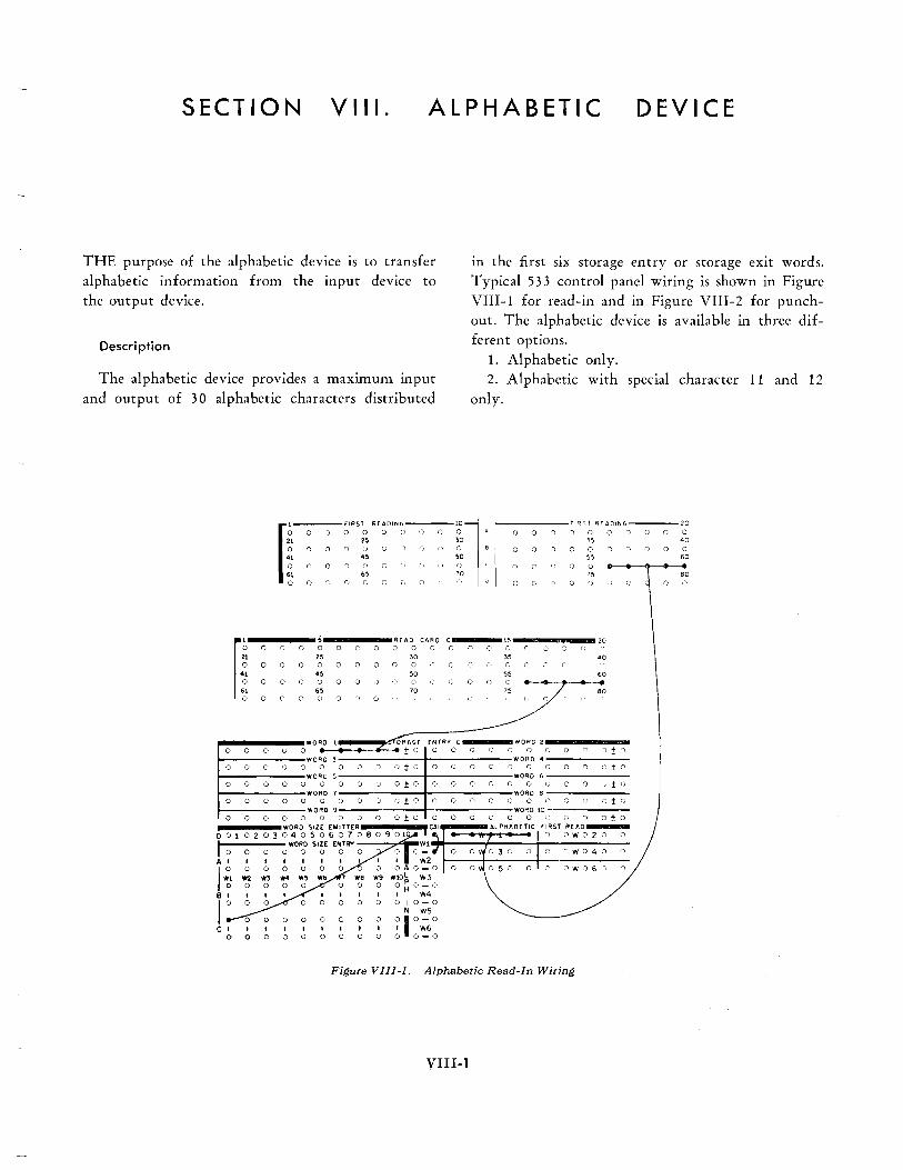
SECTION V III. ALPHABETIC D EV ICE
THE purpose of the alphabetic device is to transfer alphabetic information from the input device to the output device.
Descri ption
The alphabetic device provides a maximum input and output of 30 alphabetic characters distributed
fl j:"IRS T REAOINC>
0 () 0 0 0 0 25
() 0 () , 0 41 45 () () 0 C) n 6, 65 0 () " " 0 <]
(")
()
u
r~ 5 READ CARD
C 0 0 0 0 0 0 0 0 2. 30
0 0 0 0 0 0 0 0 0 41 4' 50 0 C 0 n 0 0 0 0
61 65 70 () 0 0 " 0 0 n 0
C 0
0
0
In the first SIX storage entry or storage exit words. Typical 533 control panel wiring is shown in Figure VIII-I for read-in and in Figure VIII-2 for punchout. The alphabetic device is available in three different options.
1. Alphabetic only. 2. Alphabetic with special character 11 and 12
only.
~l FIRST READING 20
() 0 <) () 0 0 0 0 0 0 30 35 40 () 0 0 () 0 0 0 0 0 0 0 50 55 60 0 " 0 0 70 75 60 r c 0 G 0 0 () 0 0
15 20 0 0 0 0 0 <)
35 40 () () .0 n
55 60 0 0 0
" 60 0 0 n
WORD 1 DRAGE EN TRY C WORD 2 .......
0 0 0 0 0 :t 0 G 0 0 0 () oj ± 0
"'ORO 3 wORD 4 0 0 0 " 0 0 0 0 I) ± .J 0 0 0 0 n () 0 c ± n
WORD 5 WORD " 0 0 0 0 0 0 0 0 o ± 0 () () 0 0 0 0 0 0 ,. ± " WORD 7 WORD 6
0 0 0 0 0 0 0 0 0 G ± () () 0 0 0 0 0 <) () 0 ()!:0 WORD 9 WORD 10
0 0 0 0 0 0 0 0 0 o ± 0 0 0 0 0 0 0 0 0 n oto WORD SIZE EMITTER FIRST R£AO_
001 o 2 0 3 0 4 0 5 0 6 iJ 7 :) 8 () 9 0 10 n W ;-12 () 0
I WORD SIZE ENTRY Wi 0 0 0 0 0 0 0 o- w () 4 () ()
A I I I I I I w2
I; 0 0 0 0 oAo_o .'J W () 6 "
"" W, W10~ W3 0 0 °H O - O
B I I I I W4
I 0 0 0 0 I 0-0 N W5
0 0 0 0 0 °1 0-
0 C I I I I I I I I I I W6 0 0 0 0 0 0 0 0 0 o 0-0
Figure VIII-I. Alphabetic Read-In Wiring
VIII-l
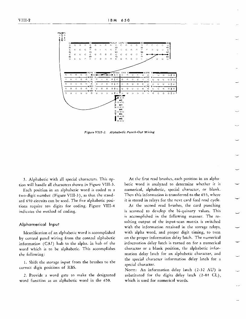
VIlI-2 IBM 650
PSU.". oSo • I • ~o
11 5 PUNCH CARD C ___ 15 201 o () 0 0 0 0 0 () 0 0 0 0 0 0 n (; C 0 0
~0002~OC003~OO o~g~OO()6 41 45 50 55 60 000 0 0 0 0 0 61 65 BO ooc,noooo 000
______ WORIDD~I.::~~:::::'O~RAGE 0:: IT C ___ _
u 0 0 0 0 .. ±O 0 0 0 0 WORD 2
0 0 0 0 0 o.i 0 WORD 3------+------WO~D 4
o 0 0 0 0 0 0 0 oio 0 0 0 0 0 0 0 0 c oio WORD 5 WORD 6
0 0 0 0 0 o ± 0 WORD 8
_____ 0_0 WO~D 7 0 0 0 0 ± 0 0 0 0 0
o 0 0 0 0 0 O±O 0 0 0 0 0 0 '- u 0 aia ------WORO 9 WORO 1O--___ ~
o 0 0 0 0 0 aia 0 0 0 0 0 0 'I 0 O!O
W1--0 W2
Ao_o ~ W3 HO-O
W4 00_0
Y W5
10-0 W6
0-0
Figure VIlI-2. Alphabetic Punch-Out Wiring
3. Alphabetic with all special characters. This option will handle all characters shown in Figure VIII-3.
Each position in an alphabetic word is coded as a two-digit number (Figure VIII-3), so that the standard 650 circuits can be used. The five alphabetic positions require ten digits for coding. Figure VIII-4 indicates the method of coding.
Alphamerical Input
Identification of an alphabetic word is accomplished by control panel wiring from the control alphabetic information (CAl) hub to the alpha. in hub of the word which is to be alphabetic. This accomplishes
the following:
1. Shift the storage input from the brushes to the
correct digit positions of RBS.
2. Provide a word gate to make the designated word function as an alphabetic word in the 650.
At the first read brushes, each position in an alphabetic word is analyzed to determine whether it is numerical, alphabetic, special character, or blank. Then this information is transferred to the 655, where it is stored in relays for the next card feed read cycle.
At the second read brushes, the card punching IS scanned to develop the bi-quinary values. This is accomplished in the following manner. The resulting output of the input-scan matrix is switched with the information retained in the storage relays, with alpha word, and proper digit timing, to turn on the proper information delay latch. The numerical information delay latch is turned on for a numerical character or a blank position, the alphabetic information delay latch for an alphabetic character, and the special character information delay latch for a special character. NOTE: An information delay latch (2-32 AU) IS
substituted for the digits delay latch (2-01 CL), which is used for numerical words.
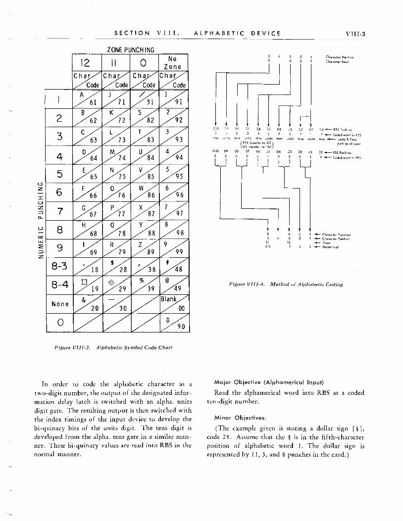
SECTION \'111.
ZONE PUNCH ING
12 II o
2
3
4
5 <.::> z 6 ::c: u z
7 ::J 0...
U 8 0::: u.J
~ 9 :::> z
8-3
8-4
None
0
Figure VIII-3. Alphabetic Symbol Code Chart
In order to code the alphabetic character as a two-digit number, the output of the designated information delay latch is switched with an alpha. units digit gate. The resulting output is then switched with the index timings of the input device to develop the bi-quinary bits of the units digit. The tens digit is developed from the alpha. tens gate in a similar manner. These bi-quinary values are read into RBS in the normal manner.
ALPHABETIC DEVICE
DlO D9 D8 D7 D6 D5 D4 2 J 9
lem units lens units lens units tens
( R3S transfer to GS ) GS transfer to PBS
D10 D9 DB D7 D6 D5 D4 B 0 0 I
5 II 3/8
3 A
D3 2
units
D3
A 3
12 I
D2 9
lens
D2
9
DJ J
VIII-3
Character Position
Character Read
DO 4-- RBS Po~ition
9 ....- Coded word in RBS units tens ~ Unih & Tens
portion of code
DI DO ~ PBS Position
I 9 ........- Coded word i"l PBS
~ Character Punched -1- Character Position
+- Zone J ~ Numerical
Figure VIII-4. Method of Alphabetic Coding
Major Objective (Alphamerical Input)
Read the alphamerical word into RBS as a coded ten-digit number.
Minor Objectives:
(The example given is storing a dollar sign [$], code 28. Assume that the $ is in the fifth-character position of alphabetic word 1. The dollar sign IS
represented by 11, 3, and 8 punches in the card.)
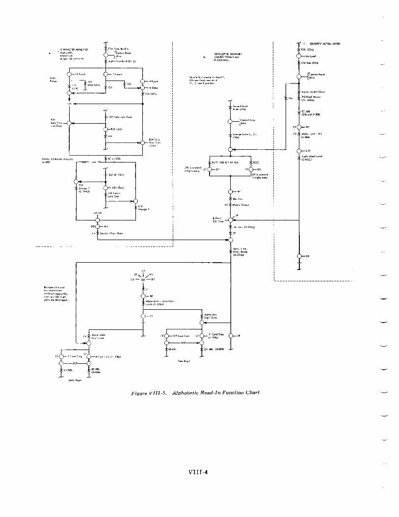
CHARACHR ANALYSIS • Alph,"""lic
Numerical or Sp<'ciol (ho,acte'
PJ5 h,teTirn., Ccnn{J5A)
(T,o".. Cf,ar(t<;'e< AnClly,j,
to 655)
8 Punch
8lime,
I--------{}- ~~~}~~: (35A)
. . ----------------------------------------------------~
!\eCQU'" unih orld Ie". pollion ere analyzed ""poralely. ~~ .. " "od odd digit ~Ol~' gre- de ... "lo?"d.
Unit, Digit
OJ
OJ,I/05
DX- OR -07
s. DEVELOP ai-QUINARY VALUES FROM CARD PUNCHING.
S ",f.arocler in Wo«! I, positie>n) coosilh of 3, and B punche.
DIOlts«Jllned CF 3 digits early
Te,),Digi'
Second Read 8.""h (1510.)
CP
Figure VIII-5. Alphabetic Read-In Function Chart
VIII-4
746
Alph".I"wl (lJA)
745 Read Alpha. Ctr. keloy.
RC 168 (358 gOO 7-301)
w.
Alpha Wo<d Latch (2-01Cl)
DB
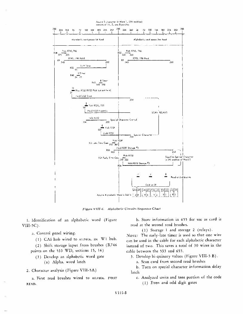
Assume S character in Word 1, (5th position) consisb of 11,3, and 8 punches
288 324 360 36 -I I 1
72 108 144 180 216 252 288 324 360 36 72 108 144 180 216 252 288 L-L II I -'I It I I I I II
;"jpna~tic cord passes 1st Read
R3() Pick R745,746
325 355
R745, 746 Hold R9
340 220 ,
1-9 Timer , R32 --------
55
1 Timer R40
54 72
11
8 Timer R41 -
180 198
_ Pick R722 (R723 Pick but not held) 27
: Hold R722 Zone
3 _ Pick R721, 723
99
: Hold R721 Numeric
Alphabetic card passes 2nd Read
R30 Pick R745, 746
325 355
R9 R745, 746 Hold
340 220
354
SCAN RELAYS
354 Special Cha,ader --
Pick R509 R35 Late Time Cam - I
252 267
Hold RS09 Stocage '1 R36 -....,1----=-----------'
260 ~30 l Pick R510
R34 Early Time Com ,..... Signifies Special Character
1310,1 325 in 5th position of Word 1
___ H_o_ld_RS_l0_S_to_'a.;;,ge_'2 ______ : J R36 ,-
11 Read ot 2nd brushes
~dea'2S j ~~~~f-D~
Assume Alpl,ebetic Word is S6215 l~ L~J L 9£J L~~J L~J
Figure VIlI-6. Alphabetic Circuits Sequence Chart
1. Identification of an alphabetic word (figure
VIIl-5C) .
a. Control panel wmng.
(1) CAl hub wired to ALPHA. IN WI hub.
(2) Shift storage input from brushes (R746
points on the 533 WD, sections 15, 16)
(3) Develop an alphabetic word gate
(a) Alpha. word latch
2. Character analysis (Figure VIII-5A)
a. First read hrushes wired to ALPHA. FIRST
READ.
h. Store information in 655 for use as card IS
read at the second read brushes. ( 1) Storage 1 and storage 2 (relays).
NOTE: The early-late timer is used so that one wire can he used in the cable for each alphabetic character
instead of two. This saves a total of 30 wires in the
cable between the 533 and 655, 3, Develop hi-quinary values (Figure VlII-5 B).
a. Scan card from second read brushes h. Turn on special character information delay
latch c. Analyzed units and tens portion of the code
(1) Even and odd digit gates
VIII·S

VIII-6 IBM 650
'09010 OX DO 01 02 1 03 1 0,, 1 0510610] 1 0809010 OX 00 1 I
"WC 8TIME
-
-f--. Alp~ Word lotch W~'d I
Figure VIlI-7. Alphabetic Read-In Timing Chart
d. Bring up the proper bi-quinary values ( 1) Read-in RBS
Refer to Figure VIII-6 and VIII-7 for timings.
Blank Position
o b jecti ve: Develop code 00.
A circuit from R38 (26A) is substituted for the second read brushes, because no scan relays are picked for the blank position at the first read brushes. Assume a blank position in word 1 alphabetic position 5. A circuit is completed through R38 (26A), R722-
4 N/ C (15B), 721-4 N/ C, and 901-4 N/ O. The remaining circuitry is similiar to the circuitry described for the dollar sign.
Sign Operation
Objective: Develop B5 and Q4 for DO. The plus sign associated with the alphabetic word
1 is provided by a 9 time pulse from R25 in the 533 (section 27A) to R746-2 N/ O (16B). The +55-volt potential is brought to the plate of the cathode follower at lIE on WD 2-01 BU. The D9 time output of the cathode follower is scanned by the switch 4G (WD 2-01 CL). The output of 4G turns on the sign delay latch. The output of the sign delay latch
develops a B5 and Q4 at 9 reader time at cathode followers 4K pin 8 and 4L pin 8 respectively.
Alphamerical Output
Major Objective:
To cause the proper double punching in the card columns, from the alphabetic information stored in a PBS word.
Minor Objectives:
(Assume that a $ IS In buffer I PBS, word 1, D9 and DI0. Figure VIII-8 concerns punching the 11. Figure VIII -9 concerns punching the 11, 3, and 8.)
1. Identification of an alphabetic word (Figure VIII-8A)
a. Control panel wiring (Figure VIII-2) ( 1) PSU wired to Alph. Out. WI
Assume (I 28 (S) is slored in 09 cnd 010 of PBS, the 5th character pos it ion of Alphabetic Word one. Code 28 couses pum:hing of 11, 3 \Jnd 8.
010 OX I DO
SwltcMd at 6U { dlodn 5,6 (WD 2- 12Bl) +~+":;""4J
s..ad.,d.,5T 1 diodln 9, 11 , 12 (WD 2- 121ll)
$wild-oed ot 7T
d'''''"' ', 9, la, ".1 I (\\'O 2 - 12CUj
Ten! ~ Digi ts Gates
Tho 9GtltS and lctchll$ shown above for 3 ;flciox limo oro repeatod in the lame manner ot a inde)! time to CQU,. pt.Inchlng of on 8.
Fip,llr/" VrIT- 9, AlphahMir P'tn('h~Of.1t Timing Chart
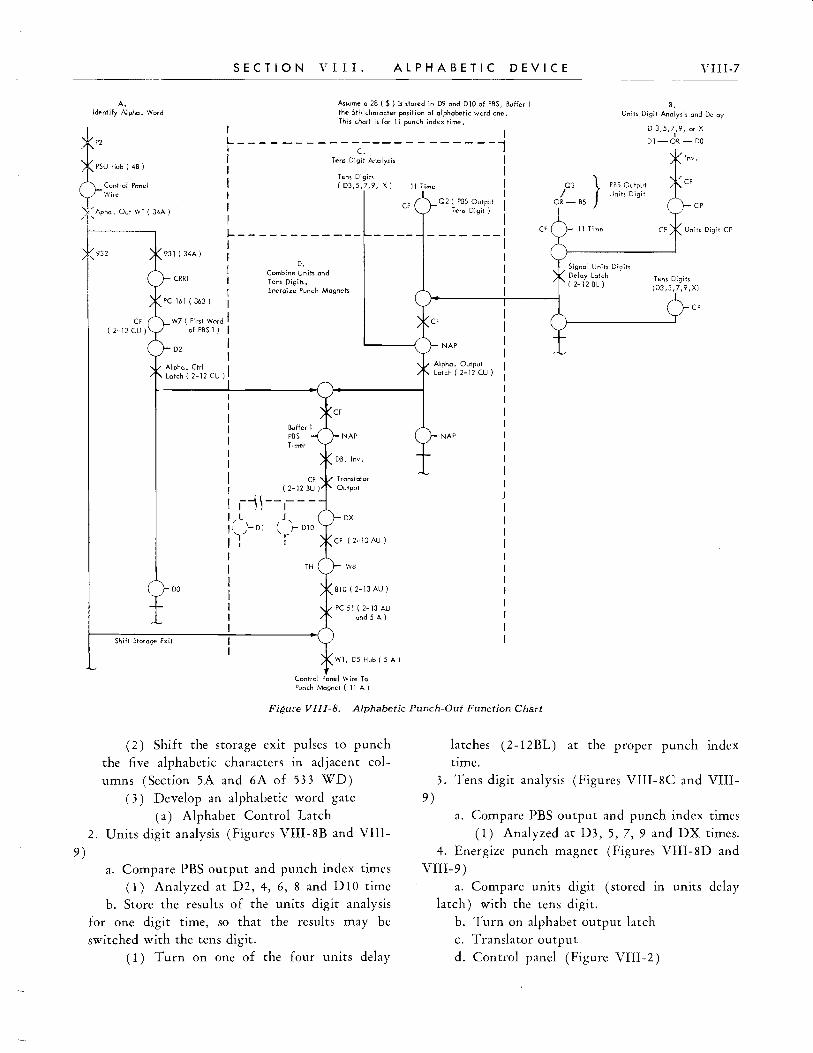
SECTION VIII. ALPHABETIC DEVICE VIII-7
A. B. Identify Alpha. Word
Assume a 28 ( S ) is dored in D9 and 010 of PBS, Buffer I the 5th character position of alphabetic word one. This chart is for 11 punch index time.
Units Digit Analysis and Delay
Control Panel Wire
CF ( 2-12 CU )
I I L-----------------------l II c. I
Tens Digit Analysis
II Tens Digits II ( D3,5,7,9, X) 11 Time
1 1 I CF 02 ( PBS Output I
Tens Digit)
I I 1------------- --- ____ 1 I I I 1
I Combine ~~ih and I I Tens Digits. I 1 Energize Punch Magnets I 1
W7 ( First Word I of PBS 1) I
DO
I I
I,..l II )-Dl I: 1 I 1 I 1 1 I
Timer NAP
DX
W8
NAP
Alpha. Output Latch ( 2-12 CU )
NAP
Shift Storage Exit
Wl, D5 Hub (5 A)
Control Panel Wire To Punch Magne. ( 11 A)
Figure VIII-B. Alphabetic Punch-Out Function Chart
03 /
OR- B5 }
PBS Output Units Digit
11 Time
Signol Units Digits Delay lotch ( 2-12 BL)
D 3,5,7,9, or X t
Dl-0R -DO
Tens Digits (D3,5,7,9,X)
CP
(2) Shift the storage exit pulses to punch the five alphabetic characters in adjacent columns (Section 5A and 6A of 533 WD)
latches (2-I2BL) at the proper punch index time.
(3) Develop an alphabetic word gate (a) Alphabet Control Latch
2. Units digit analysis (Figures VIII-8B and VIII-
9) a. Compare PBS output and punch index times
(1) Analyzed at D2, 4, 6, 8 and DIO time b. Store the results of the units digit analysis
for one digit time, so that the results may be switched with the tens digit.
( 1) Turn on one of the four units delay
3. Tens digit analysis (Figures VIlI-8C and VIII-9)
a. Compare PBS output and punch index times (1) Analyzed at D3, 5,7,9 and DX times.
4. Energize punch magnet (Figures VIlI-8D and VIIl-9)
a. Compare units digit (stored in units delay latch) with the tens digit.
b. Turn on alphabet output latch c. Translator output d. Control panel (Figure VIIl-2)
SECTION IX. MAIN POWER SUPPLY
INTRODUCTION TO THE ACME SINGLE
AND THREE-PHASE POWER SUPPLY
THE 655 houses, in addition to the read-in and readout circuitry, the power supplies for all electronic
circuits. The following list shows the power supplied and the units and purpose for which supplied.
1. Unregulated voltage Blower motors
2. 24 volts ac Buffer interlock relays
3. 230 volts unregulated Drum motor
4. Unregulated voltage, Buffers I, II, III
10 amperes 5. 115 volts at 10 am- Test equipment outlet
peres-isolated 6. Filament bring-up Filaments warm-up
voltage 7. Filament full voltage Filaments running
8. Negative 63 volts Protective bias ( in-sures no accidental writing on the drum)
9. Negative voltages Electronic circuits
10. Positive voltages Electronic circuits
11. 42 volts dc Control relays and lights
A set of push-button control switches located on
the relay gate performs the same functions as the power switches on the console of the calculator. In
dicator lights labeled POWER ON and READY indicate the power status of the machine. Control is by means of contactors (power-operated switches) and relays.
IX-l
Application
The three-phase 655 power supply may be operated from either a one- or a three-phase line source. When used on three-phase lines, the unit does not use three
phase power as such. The various loads are distributed to the phases arbitrarily. The unit may be changed for operation on alternate source of power (from one
to three or three to one phase) by changing the power cord and CB2 and rearranging the leads at the phasechanging terminal board to the right of the CB2. A bill of material is available for either change. Instructions for changing the leads for alternate source
are given in the power supply circuit diagram 2-20A.
Operation may be from a 208 or 230 volts line
source, plus or minus ten per cent. Adjustment for the different voltages is by means of jumpers on
three sets of terminals at the base of the fuse panel and the input lines to the filament transformers on
the opposite side of the machine. The jumpers and
terminals on the fuse panel are provided for adjusting the voltages to the drum motor, test receptacle, and the control relays and lights. The stabilizing trans
formers for the dc supplies have taps for two ranges of input voltage (170-220 and 200-250). The line frequency will be specified in the wiring diagram of
each machine. The frame must be at ground potential.
Regulator
The power supply makes use of stablizing transformers (Figure IX-IA) for the purpose of maintaining good voltage regulation. It is specially
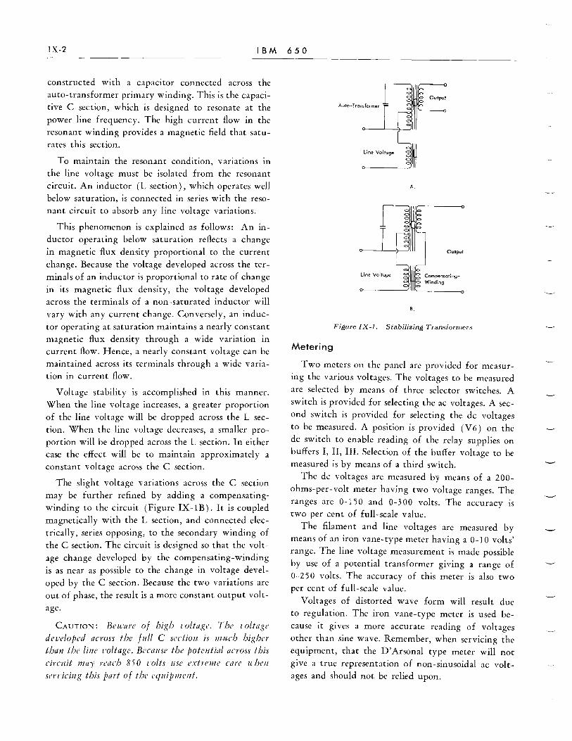
IX-2 IBM 650
constructed with a capacitor connected across the
auto-transformer primary winding. This is the capacitive C section, which is designed to resonate at the
power line frequency. The high current flow in the resonant winding provides a magnetic field that saturates this section.
To maintain the resonant condition, variations In
the line voltage must be isolated from the resonant
circuit. An inductor (L section), which operates well below saturation, is connected in series with the resonant circuit to absorb any line voltage variations.
This phenomenon is explained as follows: An inductor operating below saturation ref1ects a change in magnetic flux density proportional to the current
change. Because the voltage developed across the terminals of an inductor is proportional to rate of change
in its magnetic flux density, the voltage developed across the terminals of a non-saturated inductor will vary with any current change. Conversely, an inductor operating at saturation maintains a nearly constant magnetic flux density through a wide variation in current flow. Hence, a nearly constant voltage can be maintained across its terminals through a wide variation in current flow.
Voltage stability is accomplished in this manner. When the line voltage increases, a greater proportion
of the line voltage will be dropped across the L section. When the line voltage decreases, a smaller proportion will be dropped across the L section. In either case the effect will be to maintain approximately a constant voltage across the C section.
The slight voltage variations across the C section may be further refined by adding a compensatingwinding to the circuit (Figure IX -lB ). It is coupled
magnetically with the L section, and connected electrically, series opposing, to the secondary winding of the C section. The circuit is designed so that the volt
age change developed by the compensating-winding is as near as possible to the change in voltage developed by the C section. Because the two variations are
out of phase, the result is a more constant output voltage.
CAUTION: BellarI' of bigb l'oltage. The l'oitage developed across the full C scctiOIt is mucb bighcl' than the line l'oltage. Because fbI' potential across tbis circuit may reach 850 l'olts lise extreme cllre whcll scrl'icillg this part of flJC equipment.
Metering
Auto-Transfonner
line Voltage
A.
line Voltage
B.
Output
Output
CompetliotingWinding
Figure IX-I. Stabilizing Transiormers
Two meters on the panel are provided for measuring the various voltages. The voltages to be measured are selected by means of three selector switches. A switch is provided for selecting the ac voltages. A sec
ond switch is provided for selecting the dc voltages to be measured. A position is provided (V 6) on the dc switch to enable reading of the relay supplies on buffers I, II, III. Selection of the buffer voltage to be measured is by means of a third switch.
The dc voltages are measured by means of a 200-
ohms-per-volt meter having two voltage ranges. The
ranges are 0-150 and 0-300 volts. The accuracy is two per cent of full-scale value.
The filament and line voltages are measured by means of an iron vane-type meter haying a 0-10 volts' range. The line voltage measurement is made possible
by use of a potential transformer giving a range of 0-250 volts. The accuracy of this meter is also two per cent of full-scale yalue.
Voltages of distorted wave form will result due to regulation. The iron vane-type meter is used be
cause it gives a more accurate reading of voltages other than sine wave. Remember, when servicing the
equipment, that the D'Arsonal type meter will not give a true representation of non-sinusoidal ac voltages and should not be relied upon.

SECTION IX. MAIN POWER SUPPLY IX-3
Servicing
The power supply is so constructed that the various units are readily removed from the frame for servicing. The units are wired so that all interconnecting wires are brought to terminal boards for ease of removal.
All circuits (ac and dc) are fused or otherwise protected for current overloads. The dc branch circuits are fused by indicator-type fuses. All fuses are readily accessible for inspection and replacement.
INTERLOCKING
The individual power supplies are interlocked so that a definite sequence of turn-on and turn-off occurs. This is done to protect the equipment from possible damage due to application of voltages or due to heat accumulation. In addition, the 655 power supply is interlocked with the 652 and 653 power supplies, which operate as slave units to the 655 power supply. The corresponding units in the 652 and 653 must be operated to complete the sequence. The interlocking circuits provide for indication of filament voltage at the 652 and 653, all negative voltages on at the 652 and 653, all plus voltages on at the 652 and 653. Interlocking is also provided for blower motor failures, filament failures, blown dc fuses, and blown ac fuses. The power supply may be operated independently of the 652 and 653 by installing a set of jumpers at a terminal board supplied for this purpose (00-34 CL, Note XII).
Power-On Interlocking
When power is first applied, the blowers will be put into motion to start forced-air circulation. The voltages will be applied in such a sequence as to prevent damage to any of the components. The tube filaments will be brought up to operating temperature over a period of about one minute. The voltage is applied in such a manner as to prevent exceeding the current ratings by more than 25 per cent. When the filaments have reached operating temperature, the negative dc supplies will be turned on before the positive dc supplies.
The interlocking circuits assure that the supplies be turned on in proper sequence. The order of application of power is as follows:
1. Blowers - 63 volts
2. Filament bring-up circuit Drum motor Buffers I, II, III
3. Full filament 4. Negative voltage supplies 5. Positive voltage supplies 6. Ready light
When all the supplies in the 650, 652, and 653 have been turned on and the ready light on the console is on, the machine is in operating condition and ready to accept instructions.
Figure IX-2 shows the sequence of operations when the machine POWER-ON key is depressed. The chart shows the depression of the POWER-ON key resulting in the pick of relay 12, which in turn picks relay 4. Actually relay 4 is picked only if relay 31 (blown fuse) has not been picked and latched (00-34 AL). Relays 10 and 11 are shown as being picked by 16, 17, and 23. Actually, this circuit is further conditioned by filament ON relays in both the 652 and 653 (00-34 AL). Thus, before the negative dc voltage will be turned on, the filament voltage must be turned on in the 650, 652, and 653. In the same manner, R'3 is conditioned by negative supplies in the 652 and 653, and the ready light is conditioned by the positive supplies in the 652 and 653. When circuit failures are being analyzed, it is suggested that the charts be used for locating the general area of failure and the logics be used in finding the actual trouble.
Power-Off Sequence
The interlocking circuits provide for the removal of power in such manner as to prevent damage to the circuit components (Figure IX-3).
In general, the order of removal is as follows:
1. Positive dc voltage 2. Negative dc voltage 3. Drum motor 4. Filaments 5. Blower motors and protective bias
The blowers are left on for about five minutes after shut-down to prevent heat build-up in the units.
A POWER-OFF sequence may be initiated in several ways. (See hold circuit for relay 6 in 00-34 AL.)
er n Key ______ 1 Pow 0
R12
R16
R4 _
R7 _
RS _
R6 _
K4,
Slow
R13
R23
Slow
R9_
Kl
er Motots
er Timer
Motor
--',
~
AC On Interlock
Reduced Filament Power
.R8_
KS_
R34, 35,36 ___ filament Sense Relays
I
R29 _
R30
K6
R17_
RIO,
K2_
R24,
R3 _
K3 _
Reduced FIf. Voltage TImer
II
25,26,27 __
R18, 19,20,21,22
R1S
Ready Li~t
Warm-Up Timer
Full Filament Power
Filament Ready Relay
Negetive DC Relays
PONer Ta Negative Supplies
Negative DC Supplies
Pasiti .. DC Relay
Pasltlve DC Contactor
Pooitlve DC Supplies
Ready Relay
Power Off Sw itch +..
Power On Relay -T DC Sense Delay
1 Power On
Normal Power 011
DC Off
Auto Power 011
Slower Motors & Slas Supply Power
alowers Interlock Relay
Protective Bias Relay
AC Power Relay
T Machine & Drum Motor Power
1 I
T 4 30 Seconds
~ f.. 30 Seconds
1 I I V
~, T ------
_.-
Figure IX-2. Power-On Sequence
Ready Light
R7 I...: Normal Power Off
R3
K3
RI8,19,20,21,22
R1S, Ready light
RIO, II
R9
K2
R24,2S,26,27
Kl
Drum Motor
R8
K6
R34,35,36
Blower Timer
t17
R29,30
Power On light
K4
RI3
R23
Positive DC I Positive DC Contactor
Positive DC Supplies
Negative DC
AC Power
Negative DC Contactor
Negative DC Supplies
Iv\ain Contactor
AC On Interlock
Filament Contactor
Filament Sense
Filament Ready
Thoen
Blowers Contactor
652 - 653 Blowers
Protective Bias
I I
~ I
~ I
r
~ 1
r-. 1
5 minutes
r-.
'" ......
Figure IX-3. Power-OR Sequence
IX-4
1 T
'1 1
1
I
I
I
+ 2 }-- J
r-. ......
SECTION IX. MAIN POWER SUPPLY IX-5
DC Off Key
RS
R3
K3
RI8,I9,20,21,22
R15
Rl0,l1
K2
R24,25,26,27
DC Off
Positive DC
Positive DC Supplies
Ready
Negative DC
Negative DC (ontactor
Negative DC Supplies
Figure IX-4. DC-Off Sequence
DC On
R12
R16
R4
R5
Switch
--. TPower On I l r
r T DC Sense Delay
1 Power On
DC Off
Negative DC RIO, 11
K2
R24,25,
R3
1 Negative DC Contactor
<T .~ I Negotive DC Supp ies 26,27
K3
R18,19,
R15
Ready L
20,21,22
ight
.~
--------
Positive DC
I Positive DC Contactor
r Positive DC Supplies
I Ready
Figure IX-S. DC-On Sequence
When the power is removed by depressing the POWER
OFF key, sequence shown in Figure IX-3 will take place. Power may be reapplied by depressing the
POWER-ON key.
DC-Off Sequence
A DC-OFF sequence will be initiated when the DC
OFF key is depressed or a blown fuse is detected in a dc circuit. The DC-OFF sequence is similar to the be
ginning of a POWER-OFF sequence. The last step is the
removal of negative voltages. Figure IX-4 is an operation chart of a DC-OFF sequence initiated by depress
ing the DC-OFF key.
DC-On Sequence
When the machine power is on and the dc voltages
are off, depression of the POWER-ON key or DC-ON key
will cause a DC-ON sequence. The operation is described in Figure IX-5.
Master Power-Off Switch
A MASTER POWER-OFF switch is provided on both the console and the 655 switch panel, for emergency use only. This switch shuts off all power simultaneously. These switches are normally closed and are
connected in series. Depressing either of these switches will drop R2 causing a circuit to be completed from one side of the line through CB 1-3 coil and a 75-ohm resistor to the other side of the line when the R2A normally closed point closes. The current through CBl-3 causes CB1-1, 2, and 3 to open, reulting in removal of power from all circuits simultaneously. When the power is removed in this man
ner, it will be necessary to reset CB1 before power can be applied to the machine. All efforts should be
made to apply power to the machine as soon as pos
sible in all cases where a MASTER-POWER OFF has taken place. Thus, the blowers will prevent build-up of heat in the gates.
Figures IX-6 and IX-7 show the sequence of operations when a dc, or an ac fuse is blown respectively.

IX-6
DC Fuse Blows
R37
R31
R5
R3
K3
RI8,19,20,21,22
RlO,l1
K2
R24,25,26,27
AC Fuse Blows
R32
R6
R31
R3
K3
RI8,19,20,21,22
R 15
Ready Light
RIO, II
K2
R9
R24,25,26,27
KI
R8
Filaments
Drum Motor
Buffers 1,11,111
RI7
IBM 650
DC Fuse Relay
Blown Fuse Relay
DC Off
Positive DC Relay
Positlve DC Contactor
Positive DC Suppl ies
Negative DC Relays
Negative DC (ontactor
Negative DC Supplies
Figure IX-6. Blown DC Fuse Sequence
J AC Fuse Re lay
1 Auto Powe r Off I
1\ Blown Fuse Relay
\ Positive DC Relay I
1 Positive DC Contactor
1 ! Positive DC Supplies
I I'
-I I
Negative DC Relays !
Negative DC Contactor l\ AC Power \: I Negative DC Suppl ies I J Main line Contactor 1
1 I AC - On Interlock
!
1\\ \\
Filament Reody Relay ~\ \ \..~ Power - On Light
Blower Timer
K4
! '\ 5 Min. ~~B~I~~er~sa~n~d~~~~~.~B~ia$~C~o~nt~o~cto~r ______________________________________ ~
Figure IX-7. Blown AC Fuse Sequence
DESCRIPTION AND PURPOSE OF COMPONENTS
Contactors-115 Volts AC
KI Supplies line power to machine. Supplies power to drum motor
K2 Supplies power to negative supply primaries,
K3 Supplies power to positive supply primaries,
K4 Supplies power to blower motors and primary of minus 63 volts supply,
K5 Supplies reduced power to filaments.
K6 Supplies full power to filaments.
Relays-42 Volts DC (except fuse and sense relays)
RI Emergency OFF.
R2 Emergency OFF.
R3 Positive de.
R4 Power ON_
Picks and stays up as long as main power is on.
When dropped causes CIrcuit breaker (CBI) to open, removing all power from machines.
Picks K3; causes power to be applied to plus voltage supply primaries.
Starts POWER-ON sequence,

SECTION IX. MAIN POWER SUPPLY IX-7
R5
R6
R7
R8
R9
RIO
Rll
RI2
R13
RI5
RI6
RI7
DC OFF. Starts a DC-OFF sequence when dropped.
Auto power OFF. Starts POWER-OFF sequence when fuse blows or when a filament circuit fails ill
the 650, 652, or 653.
Normal power OFF. Starts a POWER-OFF sequence when dropped.
AC-ON Interlock. Supplies power to the timedelay relay clements (R29, R30). Turns on POWER-ON light. Provides circuit to blown fuse relay (R3 1 ) . Controls 0 per a t ion of blower timer.
AC power.
Negative dc 652, 653.
Negative dc.
Power ON.
Blowers.
Ready relay.
DC sense delay.
Filament ready.
Picks Kl. Supplies power to machine.
Indicates 652, 653 negative supplies operating.
Picks K2; applies power to negative supply pnmary circuits in 655.
When picked, it will cause (a) POWER-ON sequence if the machine is off (b) DCON sequence if the power is on and dc is off.
Picks when blower motor power is applied.
Picks when all positive supplies are operating.
Prevents setting of blown fuse circuit during turn on sequence.
Picks and stays up after filaments are at operating temperature.
RI8 +250-volt control. Indicates +250-volts operating for Read Circuits.
R19 +250-volt control. Indicates +250-volts operating for Write Circuits.
R20 + I 50-volt control. Indicates + I 50-volt supply operating.
R21 +70-volt control. Indicates +70-volt supply operating (V3).
R22 +70-volt control. Indicates +70-volt supply operating (VII).
R23 Protective bias relay.
Picked by - 63 -volt supply.
R24 - 250 volts control. Indicates - 250-volt supply operating.
R25 - 50 volts control. Indicates - 50-volt supply operating.
R26 -70 volts control. Indicates -70-volt supply operating.
R27 - 22 volts control. Indicates - 22-volt supply operating.
R29
R30
R31
R32, R33
RH, R35, R36
R37, R38
Filament timer.
Filament timer.
Blown fuse relay.
AC fuse relays.
Filament sense relays.
DC fuse relays.
Timers
Controls period of reduced voltage to filaments.
Controls period of full filament voltage prior to applying dc.
Indicates any blown fuse or filament failure in the 655, 652, or 653. This relay is of the latch-type and must be reset prior to restoring power.
Sense blown ac fuses.
Picked by filament supplies. Drop when filament circuit fails.
Pick when dc fuses blow.
BT (5-minute timer). Removes power from blower motors 5 minutes after POWER-OFF sequence.
R29 Thermal.
R30 Thermal.
30 seconds' reduced filament voltage.
30 seconds' warm-up.

SECTION x. 533 M E C HAN I CAL P R INC I P L ES
AND CIRCUITS
THE 533 Read-Punch Unit can perform all the card
reading and card punching for the 650 calculator. The read unit is almost identical to the 402 read
unit. It contains two sets of 80 brushes called the
first read brushes and the second read brushes. Figure X-1 illustrates a schematic of the read feed. The read feed operates at the rate of 200 cards per minute.
The punch unit is almost identical to the IBM Gang Summary Punch. It contains one punch station and one set of 80 brushes called the punch brushes. Figure
Firsf Reodin9 8ru~hM
W Stacker
Stop Switch
Figure X-I. 533 Read-Feed Schematic
X·l
X-2 illustrates a schematic of the punch feed. The punch feed operates at the rate of 100 cards per minute.
Punch Drive Mechanism
The power to drive the punch unit is furnished by the drive motor. The drive motor transmits power
to the gear housing through a belt. The gear housing
is almost identical to the 514.
Punch 8f'UlM Card leye, Contact
Die and St'ipp., V Stacker Rolf
~JlJL 0
Magazine I :~ I iI/j rr -.4 W
Magazine Cord Lever Contact
Di. Card Lever Contact
Punch Brushes Stocker
Figure X-2. 533 Punch-Feed Schematic

Figure X-3. Geneva Pawl Disengaging Mechanism
X-2
SECTION X. 533 MECHANICAL PRINCIPLES AND CIRCUITS X-3
'':==:P~U:NC;,:'.H BRUSHES 10 • 00000
25 30 o 0 0 0 0 0 0
45 50 000 0 G 0
65 70 000 COO
DP 6 Be DEl ENTRY_iO _____ 00000
I--Be DET ENTRY OR GP EXIT--,O OOOCCOOCOo
1 Be DEl CONTROL 10~ 00000 ~ 0 0 0 c 2,-- DP a Be DET ENTRY_30 o 0 0 0 0 0 coo 0 21-- Be DET ENTRY OR GP EXIT --30 00000 0 0 0 0 0 21 Be DET CONTROL 30 0000000000 41-- DP 8 Be DEl ENTRY --SO 0000000000 41-- Be DET ENTRY OR GP EXIT --SO 0000000000
Be_OFF 41 Be DEl CONTROL 50 .....,0000000000
61-- OP 8 Be OET ENTRY--70 000 000 0 0 0 0 61-- Be DEl ENTRY OR GP EXIT --70 0000000000 61 Be DE T CONTROL 70 o 0 0 0 0 0 0 0 0 0
Figure X-4. Double-Punch Detection Wiring
The main mechanical difference is in the design of the latch cam follower, knockoff cam follower arm assembly and the dog lock-out cam (Figure X-3). The dog lock-out cam pinned to the eccentric shaft will make one revolution per digit time. The high part of the cam is timed to prevent the geneva pawl from engaging with the geneva seven-tooth ratchet unless the punch clutch is engaged. When the punch clutch is engaged, the latch cams follower will turn, rotating the knockoff cam follower arm assembly in a counter-clockwise direction. This will prevent the dog lock-out cam from operating against the knockoff cam follower arm assembly to keep the geneva pawl from engaging in the ratchet. The geneva pawl will then be free to engage in the geneva seven-tooth ratchet. The operation of the latch cam arm also pre
vents the geneva pawl from disengaging until the punch clutch is latched.
Read Drive Mechanism
The power to drive the read unit is furnished by the same motor which supplied power to the punch unit. A pulley on the same shaft as the punch drive pulley drives the read unit through a timing belt. The read unit is almost identical to the 402 read feed. The main differences are the design of some of the feed rolls and gears to compensate for the increased speed. The read clutch has a 10-tooth ratchet, so it will engage without having to wait for a complete read cycle.
CONTROL PANEL
REFER to the 650 Magnetic Drum Data-Processing
Machine Manual of Operation (Form 22-6060).
533 CIRCUITS
(533 Wiring Diagram 254490B)
DOUBLE PUNCH, BLANK-COLUMN DETECTION
THE double punch, blank-column detection circuit is used to detect a column that contains two punches or a column that contains no punches.
Double Punch Detection Circuit (Figures
X-4 and X-5)
Refer to Figure X-4 for the control panel wiring. The Be hub is wired to the OFF hub picking relay 316 from P16 so the blank column detection circuit will be inoperative. The OPBC hub is wired to the STOP hub to pick the double punch, blank-column stop relay 3 18. The punch brushes corresponding to the columns to be checked for double punches are wired to the OP and BC OET ENTRY hubs. Refer to
Section 9A of the 533 wiring diagram. Assume that the column, wired to the first entry hub, contains a double punch. The impulse from the first hole will pick relay 319. Relay 319 will pick relay 320, and both relays will hold for the remainder of the feed cycle. The impulse from the second hole will go through relay point 320-2 N/O and pick relay 317.
At the beginning of the next feed cycle a OPBC OET error will result by picking relay 318. The following is the circuit to pick relay 318: P7, 315 -2 N/O, 317-2 N/O, DPBC wired to the STOP hub, relay 318
pick coil. Relay 315 is picked through the circuits set up by the die card lever. Relay 318-4 N/C point opens and de-energizes relay 160. Relay 160-4 N/O point opens the circuit to the punch clutch magnets. Relay 318-3 N/C point opens to prevent the punch start key from operating the punch feed until the error circuits have been reset. Relay 318 will stay energized until the reset key is depressed.
8 9 13 14 14 2 3 5 6 7 9 I , Ii " ? III ~ 1 , ", 1 i i " i " I I , 12
Punch Brush Card Lever Contact
ReI. 158 Pick & Hold
Die Card Lever Contact
ReI. 155 Pick & Hold
Rei. 314 Hold
PI ReI. 315 Pick
3:s--'4.45
Rei. 315 Hold P6 -----. -- - 14.2
I Hole Rei. 319 Pick -1.0 1.3
Rei. 319 Hold P6 --- -- 14.2
8 ReI. 320 Pick P -1.5 1.85
P6 ReI. 320 Hold ---- -- 14.2
4 Hole ReI. 317 Pick
4.04.3
P6 - _____ -- ReI. 317 Hold - 14.2
R.I. 316 Pick PI6 - 1
9.35 9.8 I
P6 Rei. 316 Hold -------------- - --- - 14.2
OP BC Hub is Wired to the Stop Hub
Rei. 318 Pic P7 1-
13.7 14.15
Reset Key I Rei. 318 H old
Figure X-So Double-Punch Detection Timing Chart
);,·4

SECTION X. 533 MECHANICAL PRINCIPLES AND CIRCUITS X-5
Blank Column Detection Circuit (Figure X-6)
Refer to Section 9A of the 533 wmng diagram. Wire the punch brushes to the DP and BC DET ENTRY hubs from the columns to be checked. \x'ire the DPBC hub to the STOP hub; the double punch,
blank-column stop relay 318 will be picked when an error occurs. With this wiring the double punch detection circuits will be operative, as well as the blank column detection circuits.
For the machine to indicate that all columns checked have at least one punch, relay 316 must be picked. The circuit to pick relay 316 is from P 16 through the normally open points of each relay, which is picked by the first digit impulse, in each position (relay 319-2 for position one). There may be a maximum of 80 of these points in series if the machine is equipped with 80 positions of DPBC de
tection. If only the first 10 positions are used, wire from the BLANK COLUMN DETECTION CONTROL hub
number 10 to the high order hub, which may be the 80th position. This will short out the normally open points of the unused positions. The blank column detection control hubs must always be wired to provide a circuit around all unused positions.
Assume position number 1 is wired to a blank column. Relay 319 will not be picked and relay point 319-2 N/O will remain open to prevent relay 316 from picking. Relay point 316-2 N/C remaining
;-:-:':"':} ":'"'~-:-:-;~., ~ 4~ ~ o coo C -:;", 0 .,:,
~ 6~ ro o~oooooooo 6~
1_ DP Ii BG U ENTRy_tO
1--8e OET ENTRY OR GP EXIT--10 ~f 00000002)00 ~,
1 ___ Be DET CONTROL ---10
0\:)000:)000
""" ,"c,",,-,.o1 o 0 0 0 0 0 ',' 0 t-) "
35 40 00000000:]0
55 BO 0000000800
15 80 ooooooooc'-:;' U_OP8 Be D£T [NTRY_20 oooooooooc; u-- Be OET ENTRY OR Gf' EXIT --20 0000000000
21 __ OPe, Be OET ENTRY __ 30 31-- OP e Be DET ENTR'I' __ 'O ooacoocooo 0000000000 ,, __ Be OET ENTRY OR GP EXIT --'0 [ Be OET ENTRY OR GP E~IT --'0 0000000000 ~J 0 O(lQOOOOO ,,---Be DET C(WTROL---30 31 Be DET CONTROL --'0 o 0 0 0 0 0 0 0 0 0 ,r..: 0 0 0 0 0 a a 0 0 0
ci~ OPOS B~ OE~ EN~RY~5g~~l r~~ 01"0 Be OE~ EN~RY-:;--;-~ '1 __ Be DEl ENTRY OR GP EXIT --:\0 r--51-- BC DEl EN OR {,P EXIT --60
o 0 0 0 0 0 a 0 0 0 ~ ... ~O 0 0 0 0 0 0 0 0 '1--_BCOETCONTROL ___ 50 51-- BeDETCON l --60 000008(:000 A', 000000 OQO 61 __ 01"5 Be OET ENTRY __ 10 11--01"& Be OET ENT --80 0000000200 AI' 0000000 OC 61-- Be OET ENTRY OR GP EXIT --10 11-- Be OET ENTRY OR Gf' (XII 80 0000000000"'0 0000000',)
~-o-o-~G O~T C~TRO~-O-O-~! r.Q ~~ ~C D~T C~TFW~ a 0
Figure X-6. Double-Punch and Blank-Column DetecUon Wiring
closed will provide a circuit to pick relay 318. A double punch or blank column error is detected when relay 318 is picked.
Double Punch Detection Exit
These hubs may be wired to the punch magnets for a gang punch operation.
PUNCH DELAY
THE PUNCH DELAY IN hub will accept any punch impulse from 13.8 to 9.8. During the following punch cycle, the OUT hub will emit an impulse between 13.7 and 14.5.
Punch Delay Application
Storage exit C and storage exit B word 1 are selected by control information to punch into different columns. When the card passes the punch brushes, one cycle after it had been punched, a co-selector must be used to select the corresponding punch brushes for double punch, blank-column detection. The co-selector must be controlled by a one cycle delayed control information impulse.
Punch Delay Circuit
Refer to section 4 B of the 53 3 wmng diagram. The input impulse will pick relay 306, which will
hold to 9.8; at 9.3 through the relay 306-2 N /0
point, relay 307 will pick. Relay 307 will hold until 14.2 of the next feed cycle through P6. A punch delayout impulse will be obtained through the 307-2 N/O point and P21 between 13.7 and 14.15 of the next feed cycle.
CONTROL INFORMATION
CONTROL information permits the operation of devices such as selectors and punch delay from information that has been stored or developed in the 650. The device utilizes the tenth word of punch-buffer storage, and the impulses produced are brought out at ten sets of hubs at AK to AM, 55 to 64 on the control panel. Any control information hub will emit an impulse when the corresponding position in punchbuffer storage has an eight stored in it. This impulse will occur at 14 punch index time.
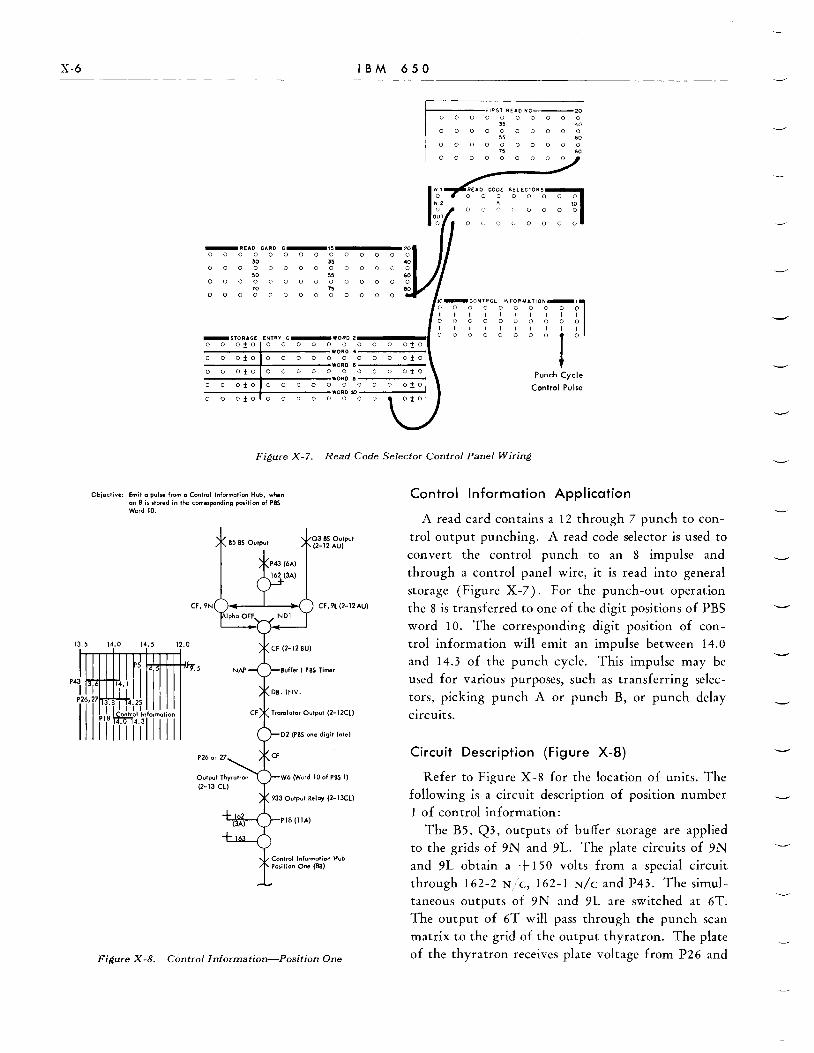
X-6
13.5
IBM 650
0 0
0 0
0 0
0 0
nRST REAOING--__ 20
0 0 0 0 0 0 0 0 35 40
0 0 0 0 0 0 0 0
" 60 0 0 0 0 0 0 0
" 80 0 0 0 0 0 0
READ CODE SELECTORS~ o 0 0 0 0 0 0 0
, to o 0 i} , (; 0 0 0
o 0 G 0 0 0 0 0
_READ CARD C_15 20 o 0 0 0 0 0 000 0 000 0
30 3:5 000 000 0 0 0 0
'0 ,. 0 0 0 0 0 0 0 0 0 0
70 " 0 0 0 0 0 0 0 0 0
_STORAGE ENTRY C WORD 2 0 0 o ± 0 0 0 0 0 0
WORD 4 0 0 0:1:0 0 0 0 0 0 0
WORD 6 0 0 0:1:0 0 0 0 0 0 0
WORD 8 0 0 0:1:0 0 0 0 0 0 0
WORD 10 0 0 o ± 0 0 0 0 0
0 0
0 0
0
0
0 0
0 0
0
0
0
10_GO~TROL INFORMAT10N_tl o COO 0 0 0 0 0 0 I I I I I I I I I I o 0 0 0 0 0 0 0 0 0 I I I I I I I I I I
000 000 0 0 I 0
Punch Cycle
Control Pulse
Figure X-7. Read Code Selector Control Panel Wiring
Objective: Emit a pulse from a Control Information Hub, when an 8 h stored in the corresponding position of PBS Word 10.
B5 B5 Output
14.0 14.5 12.0
03 as Output (2-12 AU)
Figure X-So Controllniormation--Position One
Control Information Application
A read card contains a 12 through 7 punch to control output punching. A read code selector is used to convert the control punch to an 8 impulse and through a control panel wire, it is read into general
storage (Figure X-7). For the punch-out operation the 8 is transferred to one of the digit positions of PBS word 10. The corresponding digit position of control information will emit an impulse between 14.0 and 14.3 of the punch cycle. This impulse may be used for various purposes, such as transferring selec
tors, picking punch A or punch B, or punch delay circuits.
Circuit Description (Figure X-8)
Refer to Figure X-8 for the location of units. The following is a circuit description of position number 1 of control information:
The B5, Q3, outputs of buffer storage are applied to the grids of 9N and 9L. The plate circuits of 9N and 9L obtain a -+ 150 volts from a special circuit through 162-2 N,C, 162-1 N/C and P43. The simultaneous outputs of 9N and 9L are switched at 6T. The output of 6T will pass through the punch scan matrix to the grid of the output thyratron. The plate of the thyratron receives plate voltage from P26 and

SECTION X. 533 MECHANICAL PRINCIPLES AND CIRCUITS X-7
P27. The output of the thyratron provides a circuit to the control information output through the 163-1 N/C point.
READ CODE SELECTOR
REFER to Section 11 of the 533 wiring diagram. Each read code selector has two input hubs (IN 1 and IN 2) and one exit hub (OUT). The outputs of the OUT hub may be an 8, 9, or no impulse, depending on how the IN hubs are conditioned. The chart below illustrates all the possible conditions and results.
In 1 In 2 Out one 12-7 impulse one 12-7 impulse 8 impulse one 12-7 impulse no impulse no impulse no impulse one 12-7 impulse no impulse no impulse no impulse 9 impulse
The read code selector operation sequence chart (Figure X-9A) shows that the IN 1 hub is impulsed one cycle before the IN 2 hub. The output from the out hub is obtained during the second feed cycle.
Read Code Selector Application (Figure X-7)
All problem cards that contain an X in column 80 will have their answers punched in columns 20 to 25 instead of columns 10 to 15. The IN 1 hub will be wired from column 80 of the first reading. The IN 2 hub will be wired from column 80 of the second read. The OUT hub will be wired to any digit of storage entry word 10. When a card containing an X in column 80 impulses the IN 1 and IN 2 hubs, the OUT
2BB I
CARD PASSING 1ST READING
"X" R659P
INI -27 36
2BB I
CARD PASSING 2ND READING
RB ____ ~R~65~9 ______ ~--
27 352
(0) RSO not plugged
R660P R7 -
31B 34B
R9-------R660~H-----340 220
"X" R66IP IN 2 -
2736
R661H R9 ----~-----
27 220
OUT B R24 -
IBB 200
2BB I
hub will emit an 8-impulse, which is eventually placed in one of the digits of word 10 of PBS. At 14 time during the next punch cycle, a corresponding hub of control information will emit an impulse. This impulse will transfer a selector so the punching will occur in columns 20 to 25.
If the OUT hub emits an 8 impulse, control information will emit an impulse at 14 time. If the OUT
hub emits a 9 impulse or no impulse, control information will not emit an impulse.
Circuit Description (Figure X-9A and 533-12A)
Any 12 through 7 impulse into the IN 1 hub will pick relay 659. Relay 659 will hold into the next feed cycle where it will pick relay 660. During the cycle in which relay 660 is picked, any 12 through 7 impulse into the IN 2 hub will pick relay 661. The 660-2 N/O and 661-2 N/O points will provide a circuit to emit an 8 impulse out the the OUT hub. If neither relay 661 or 660 is picked, the OUT hub will emit a 9 impulse. If just one of the two relays is picked, the OUT hub will not emit an impulse.
RSO (Read Second Only) Wired (Figure X-9B)
When RSO (533-12A) is plugged, the 655-2 N/O point shorts out the one cycle delay circuit and provides a circuit from the IN 1 hub to relay 660. To obtain the desired results from the example previously discussed, the IN 1 and IN 2 hubs must be wired from the second reading brushes.
2BB I
CARD PASSING 1ST READING
R655 & 691
(b) RSO plugged
2BB I
2BB I
CARD PASSING 2ND READING
"X" R660P IN I -27 36
R9 R660H
27 220
"X" R661P IN 2-
27 36
R9 R661H
27 220
OUT B R24 -
IBB 200
Figure X-9. Read Code Selector Operation

x-a IBM 650 ~------------~-----.~
READ FEED CIRCU ITS (Figure X-10)
The read clutch magnet in the 533 is under control of R7 1 and 2 points in section 13B of 533 wiring diagram. Relay 7 hold coil (14A) is operated for the first three card feed cycles under control of the read start key and card lever circuits. During the third card feed cycle, R9 is picked by action of the card lever circuits and R9-5 N/C points (14A) are opened. Control of card feeding is transferred to the 650. The next pulse to pick R7 comes to the pick coil as a result of a code 70, 73, or 76 in the 650. The code which is involved depends on the buffer to which the 533 is attached.
1. First feed cycle. Relay 7 hold coil is operated by a circuit from 50V-3 (14A) through the stacker stop, read start 1 key, 10-4 N c, 13-4 N/C, 16-3 N c, 142-4 N/O, 8-4 N/C, 9-5 N/C, and R7 hold coil.
2. Second read feed cycle. Relay 7 hold coil is operated by a circuit from 50V-3 (14A) through the stacker stop, 142-3 N/O, 13-3 N/C, 1-2 N/O, 16-2 N/O, 13-5 N/C, 2-3 N/O, 5-2 N/C, 6-2 N/C, 9-5 N/C, and R7 hold coil.
3. Third read feed cycle. Relay 7 hold coil is operated by a circuit from 5 OV -3 through the stacker
stop, 143-3 N/O, 13-3 N/C, 1-2 N/O, 16-2 N/O, 13-5 N/C, 2-3 N/O, 5-2 N/O, 3-3 N,O, 6-2 N,/C, 9-5 N/C and R7 hold coil.
4. All read feed cycles after the third. Control of feeding of cards passes to the 650 during the third card feed cycle by the pick of R9. The circuit to pick R9 is from 50V-3 through the stacker stop, 142-3
N/O, 13-3 N/C, 1-2 N/O, 16-2 N/O, 13-5 N/C, 2-3 N/O, 5-2 N/O, 3-3 N/O, 6-3 N/C, 3-4 N/O, R12, and R9 pick coil. R7 is operated by a circuit through R46 (14A) R7 pick coil, RC4, and a thyratron in the 655. Refer to Input-Output Codes, Section 7.
To provide a machine stop and a feed check light
if extra feed cycles occur. Extra feed cycles could be caused by improper clutch adjustments. R7 would not be operated, allowing R-cam 28 to drop R142 (l3B) at 295°. R142-3 N/O points allow R-cam 19 to drop R9 (14B) at 228°. With R9 down, the 650 loses control of the 533 read feed, providing a machine stop. R142-2 N/O (2B) provides a circuit to the feed check
light.
PUNCH FEED CIRCUITS (Figure X-ll)
The punch clutch magnet in the 533 is under con
trol of the R160-4 points in section 4A of the 533
wiring diagram. R160 pick coil (4A) is operated
initially by a circuit through the punch start key
(3A). R160 holds for the two cycles of run-in. After
the run-in, control of punching is transferred to the
650 by the pick of R161. Any punch feed cycles
after the run-in are provided by the pick of R160
( 4A) through the 161-2 and 166-2 points. R166 is
operated by the development of a code 71, 74, or 77
in the 650. The code that is involved depends on the
buffer to which the 533 is attached.
1. First Punch Feed Cycle. Relay 160 pick coil is
operated by a circuit from 50V -3 through the punch
start 1 key, 318-3 N/C, 155-6 N/C, 158-5 N/C, CRPl, and R 16 0 pick coil.
2. Second Punch Feed Cycle. Relay 160 holds
through 160-1 N/O (4A) and P13 until 9.2 of the
first punch feed cycle. R160 holds from 9.2 to 9.7
through 160-2 N/O, 156-2 N/C, 143-3 N/O, 155-1
N/O, and 157-2 N/O to 50V-3. R160 then holds
through 160-1 N/O and P13 until 9.2 of the second
punch feed cycle.
3. All Punch Feed Cycles after the Second Con
trol of feeding cards passes to the 650 after the second
punch feed cycle by the pick of R161 (4A) calculate
interlock. R161 is operated by a circuit from 50V-3
through PI, 158-1 N/C, 155-5 N/O, and R161 pick
coil. R161 holds through 161-1 N/O, 143-3 N/O, 155-1 N/O and 157-2 N/O. The punch start relay,
R160, is now under control of the 166-2 N/O points
(4A). R166 is operated by a circuit through P25,
R166 coil (5A), PC32, and a thyratron in the 655.
Refer to Input-Output Codes, Section 7.
To provide a machine stop and a feed check light
if extra feed cycles occur. Extra feed cycles could be
caused by improper clutch adjustments. R166 would
not be operated, allowing P-cam 4 to drop R143
(3A) at 13.6. With R143 down, tl;1e 650 loses con
trol of the 533 punch feed. R143-2 N/C (2B) pro
vide a circuit to the feed check light.

~ '0
Hopper Card lever
R4
R2
Hopper C
Read Start Key
R4
Rea
7-1 N/O
288 348 48 108 168 228 288 348 48 108 168 228 288 348 48 108 168 228 288
2ND READ FEED CYCLE 3RD READ FEED CYCLE 1ST READ FEED CYCLF F'nt Cord Pos~es ht Read First Cerd PosSoes 2nd Reod
RIP & H
R142P 6-1 N/C
160 190 160 190 150
R142H R142H I
308 295 308 295 308
onloet (R 18) Rll &161' RII & 161' R 11 & 161'
20 260 20 260 20 260
RIIH R4
190 160 190
Upper Cord Lever Contact (R 1) ~ R2P R2P
220 270 220 270 220 270
R2H R3
R2H
250 225 250 225 250
R5P R2-- R2...!!...
150 200 150 200
R4 R5H
190 160 190
RJP lower Cord Lever Contoct (Rl) _
RJP
220 270 220 270
R3 R3H
250 225 250
R6P
150 200
R4 190
R9p R12 _
122 140
RlP 16-3N/C
RlP 2-3N/O-- 16-2N/O 3-3N/O ~'6-2N/O
I 220 260 I 220
260 I I I R7H R7H R7f-i
R4 R4 160 160 160
J Clutch Read Clulc~ Read crutch R47 7-1N/O- R47
''''0 l'::' 294 294
RI First Cord to RBS
9' 2160
"12" 'I( • R ~,7
. 3,01312
R9 Down R16Down R 11 Up
1+ Ini'iol Erase
I
Figure X-lO. 533 Read-Feed Run-In Timing Chart
288 348 48 108 168 228 288
FEED \ 4TH READ FEED CYCLE
LATCHED
295
Rll & 161'
20 260
R llH
160 190
R 16H
R2P
220 270
R2H --225 250
R5P
150 200
R5H
160
RJP
220 270
R3H
225 250
R6P
/ 150 200
R6H
160 190
R9H
CRRJ RlP
~I 244 250
R7H R46 ----'-;10
Read Clutch 7-1N/O- R47
1\ 294
RI Second Card to RBS
9' 216'
( Stort 650 Code 70
)
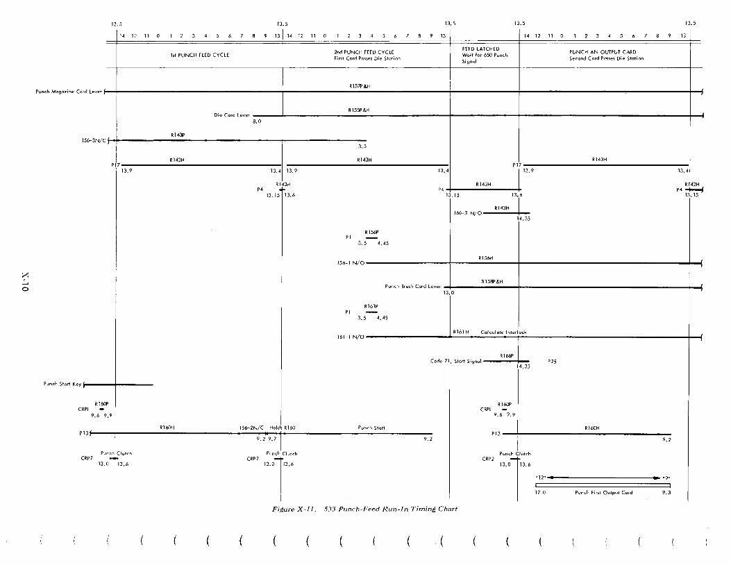
~ ~
o
13.5
14 12 \I
lot PUNCH FEED CYCLE
13.5
13 I 14 12 \I 0
2nd PUNCH FEED CYCLE First Cord Passes Die Station
RI57P&H
13.5
13
FEED LATCHED Wait for 650 Punch Signal
13.5
14 12 \I
PUNCH AN OUTPUT CARD Second Card Posses Die Station
13.5
13
Pvnch Magazine Card lever f J
RI55P&H Die Cord lever ______ -+ ________________________________________ -+ ________________ ~-----------------------------------------+ __ ~ 8.0
RI43P 15~3N/C~f~I~--------~~:-------------------_1----------------~
3.5
RI43H PI7 I
13.9 13.4 13.9
P4 RI43H
13.15tI3.6
RI43H
R156P PI
3.5 4.45
PI7 13.4
P4 I 1
13
.
9 RI43H
13.15 13.6
RI43H I 166-3 N/O 14.35
156-1 N/O R 156H
RI58'&H
RI43H
13.4
R143H P4~
13.15
Punch Brush Card Lever ~I----------------__Ir_--------------------------------_+......j 13.0
R161P PI
3.5 4.45
R161 H Calculate Interlock J6J-JN/O------------------r-------------;------------------------------------+~
RI66P . J I Code 71, Start Signa 14.35 P25
Punch Start Key .. l----+-----RI60P Rl60P
CRPI CRPI 9.6 9.9 9.6 9.9
RI60H PI31 15~2N/C Hold. RI60 II I 9.2 9.7 . 9.2
Punch Start
9.2
RI60H PI3---t-------~~~--------
CRP2 ':::r' CRP2 Punch Clurch
"'1'" I
CRP2 :;::1':~: "12" • .. "9"
Punch First Output Cord 12,0 9.3
Figure X-II. 533 Punch-Feed Run-In Timing Chart
( ( (
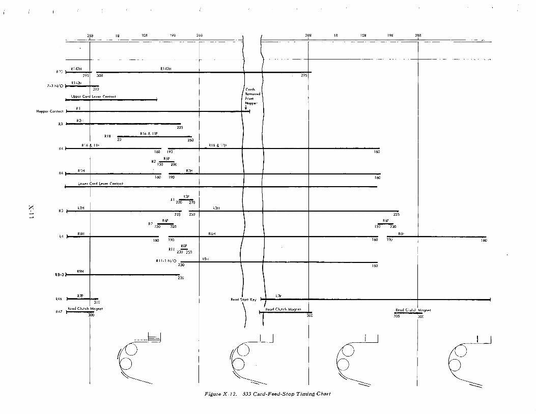
28B 18 lVe IY" leH; 2t1l:S Ie lVe lye lHH
R?8 RI42H R 142H
295 308 295
7-3 N/O RI42H
310 Cords
Upper Cord Lever Contact Removed From Hopper
Hopper Contoct R I t
R2H R3
225
R 18 RI6 & liP
20 260 RI6 & IIH RI6 & IIH
R4 160 190 160
R5P R2_
150 200
R4 RSH R5H
160 190 160
lower Cord Lever Contoct
R3P R I 2i0"'""270
~ R3 R3H R3H
225 250 225
R6P R6P R2 -150 200 15r-"200
R4 R6H R6H R6H
160 190 I 160 190 160
RSP RII -230 250
RII-I N/O R8H
230 160
R9H R8-3
230
RlP RlP
310 Read Stort Key
Read Clutch Mognet ) Read Clutch Mognet Read (I utch Magnet I 300
I 300 705 300
R46
R47
-----bd I I I I I I ~
j j -
~ ~ ----c:: --.::::::: ~
Figure X -12. 533 Card-Feed-Stop Timing Chart

X-12 IBM 650 ----- -------------------------~ ----------
CARD FEED STOP
WHEN a read feed failure occurs, the 650 loses control of the feed circuit. The 650 will progress to the next feed cycle and hang up. In order to restore the card feeding back to normal and calculate all the cards, the following procedure must be followed:
1. Remove the cards from the hopper.
2. Run all the cards into the stacker by depressing the read start key.
3. Remove the last two cards from the deck in the stacker and place them on the bottom of the deck yet to be fed. These cards have not been calculated.
4. Run the uncalculated cards into the feed in the normal manner. After the third run-in cycle the 650 will automatically signal for a feed cycle to calculate the first card.
Circuit Operation (Figure X-12)
Refer to sections 13 and 14 of the 533 wiring diagram. When a card fails to feed from the hopper, the upper card lever contact will open and relay 2 will de-energize. Relay 2-3 N/C points will provide a circuit to pick the card feed stop relay 8. Relay S
will hold under control 11-1 and 13 -3. Relay 8 - 3 points will open the hold circuit to relay 9 to prevent the calculating of the last two cards during the runout. Relay 8-4 points will render the start key useless until the cards have been removed from the hopper.
After the cards are removed from the hopper the read start key will provide a circuit to pick relay 7 and cause feed cycles to run the cards into the stacker. The last two cards that were fed must be placed on the bottom of the uncalculated deck. This deck should then be run-in using the read start key. The three run-in cycles will take place in the normal manner.
END OF FILE
REFER to the end-of-file sequence chart (Figure X-
13) .
When the hopper becomes empty, the hopper contact will open and the read feed will stop at the end of the current feed cycle. If the read start key is depressed, all cards will feed into the stacker, and the last three cards will not be calculated. If the endof-file key is depressed, the read feed will be placed under the control of the 650. Three automatic feed cycles will occur, and the last three cards will be calculated. The read start key is used to run the remaining cards into the stacker.
Circuit Operation
Refer to sections 13 and 14 of the 533 wiring diagram. The hopper contact opens at 220 degrees and dc-energizes relay 1. Relay 1-4 N/O points opens the pick circuit to relay 9. With relay 9 de-energized, the read feed will not operate under the control of the 650. Relay 10 is picked by the end-of-file key n urn ber 1 through the following circuit: 50 V -3, stacker stop switch, 142-3 N/O, 13-3 N/C, 1-4 N/C, 6-4 N/O, 13~6 N/C, R14, end-of-file key number 1, relay 10 pick coil. After relay 9 is picked through the 10-3 points, the 9-2 N/O and 9-3 N/O points (section 13B) will be used to enable the 650 to control the read feed.
After the third feed cycle, the last card will be calculated. The 650 will then lose control of the read feed. Relays 9 and 10 will be allowed to drop out by the second read delay relay 6-4 N/O point. The 10-4 N/C and 9-5 N/C points will now provide a circuit from the read start key to pick relay 7 so the remaining cards in the feed may be run into
the stacker.
PUNCH CODE SELECTOR
REFER to section lIB of the 533 wiring diagram. Punch code selectors may be picked by any punch impulse from 13.8 to 9.8. The selector will hold for the remainder of the punch cycle through P19.
~-

i-1 , w
288 18 1
108 1
198 1
last Card leaves the Hopper
Hopper Contact
220 RI
R16& II P
288 288
l I ( I Read Clutch latched
R18 20
RI6 & II H
Hopper Contact
R4 160 190
R2 P RI
220 270 R2 H
R3 I 225 250
R5 p R2 --
150 200
RSH R4 I 160 190
R3 P
220 270
R3 I R3 H 225 250
R6 P
150 200
R6 H
R4 I 160 190
RI42 P
R16& II H
Upper Card Lever Contact
R2 H
R5 H
LO"Ner Card lever Contact
R3 H
R6 H
RI42 P
18 I
108 I
160
198 I
R5 P
286
225
R2 --150 200
160 190
R3 P
220 270
225 250
R6 P
150 200
160 190
R5 H
R3 H
R6 H
R142 P
18 I
108 I
198 I
160
R6 P
288
225
150 200
R6 H
160 190
R 142 P
2421310
18 108 1
198
160
R4 190
266
R142 P
Read Clutch latched
288 18 I
106 I
198 1
Run Cord Out of Feed
160
u-, m-';" ! '" .~ 1_ """ !" I .~ r ." " I I I ·
R142 H :=rIO R142 H ----L. ____ ~R~142~H~ ________ _+I~I---I~1 RI42 H
R9 Rl- 4
R7 P R46 2421310
Read Clutch Magnet
R47 199j294
R9 ! ~
R46: 1 I 310
Read .Clutch f.Aagnet
TI294
295 308
R7 P
24~J31O Read Clutch Magnet
I 99j294
295 308
R7 P
240310 Read Clutch N\agnet
199j294
Figure X-13. 533 End-of-File Timing Chart
RI3 Read Stort
295 308
Key R7 P
!TT31O Read Clutch Magnet
TIm
288

X-14 IBM 650
_P1JNC.H CARD C 15 a 0 0 0 a 0 0 C
30 35 G 0 0 G a 0 0
50 a a a 0 0 0 ()
70 a :) 0 0 0 0 0
_STORAGE OIT C ___ _
o±a 0 a a 0 a
a±a a a a 0 a
o±o a 0 Gao
o±a a a 0 0
ota 0 0 0 0 0 IIO_CONTROL IN R o 0 0 0 0 , , I I o 0 0 a 0 0
I I I I 000 000
a
G
a
:)
I PU _ P\JNCH CODE SELECT 000 0 0 0 0 10 5 o T 0 a a a 0 0
aNo 0 a 0 a 0
oCo 0 0 0 0 0
~1 0 G
40 C 0 a
60 0 0 a
80 a 0 0
0
Figure X-l4. Punch-Code-Se/ector Control Panel Wiring
Punch Code Selector Application (Figure X-14)
The units position of word 2 of storage exit C emits a digit impulse. This impulse should normally punch a hole in column 35. The units position of control information emits an impulse, transferring punch code selector number 2. The digit impulse will then pass through the transferred point of the selector and punch a hole in column 75.
CO-SELECTORS
REFER to section lOB of the 533 wiring diagram. A co-selector may be picked by either a punch impulse or a read impulse. The hold circuit is determined by control panel wiring to the hold punch or hold read hubs.
If a co-selector is to be used for a punch cycle, a punch impulse must be used to pick the selector. The hold punch circuit must be used to provide a hold circuit. The co-selector can be picked and held from 13.8 to 9.8 of a punch cycle.
If a co-selector is to be used for a read cycle, it must be picked by a read impulse and held through the hold read circuit. The co-selector can be picked and held from 340 to 220 degrees of a read cycle.
PILOT SELECTORS
REFER to section lOA of the 533 wmng diagram. A pilot selector may be picked by a read impulse or a punch impulse. The XPU and DPU hub must receive a read impulse to transfer the selector. The IPU hub may receive a read impulse or a punch impulse to transfer the selector. The read or punch wired hold circuit should be used to correspond to the pick impulse.
The XPU and Dl'U provide a cycle delay; for example, an impulse from the first reading brushes will transfer the selector when the card passes the second reading station.
---
---