600 v coolmos™ c7 design guide - infineon technologies
TRANSCRIPT

1 Revision1.0, 2015-05-20
About this document
Scope and purpose
Describe Infineon latest high-voltage Superjunction (SJ) MOSFET technology 600 V CoolMOS™ C7
characteristics. The major advantage of the Superjunction MOSFET technologies applying in 600 V C7 SJ MOSFET and achievable application performance will be discussed in detail. A clear classification will be
made between 600 V CoolMOS™ C7 and existing CoolMOS™ series at the technology point of view and their application performances. Finally, a design guideline using CoolMOS™ C7 will be given for achieving high
efficient power conversion for all the relevant topologies with robust designs and safe operation.
Intended audience
This document is intended for design engineers who want to improve their high voltage power conversion
applications.
Table of Contents
1 Introduction ................................................................................................................................... 3
1.1 Technology description ...................................................................................................................... 3 1.2 Super junction (SJ) principle .............................................................................................................. 3
2 Technology comparison of CoolMOS™ CP, 650 V C7 and 600 V C7 .................................................. 6
2.1 Target applications ............................................................................................................................. 6
2.2 Electrical characteristics: General Overview ...................................................................................... 6
3 CoolMOS™ 600 V C7 features and application benefits .................................................................. 8
3.1 Low QG, QGD .......................................................................................................................................... 8 3.2 Tuned COSS Curve .................................................................................................................................. 9 3.3 Fast switching transition (dv/dt) ........................................................................................................ 9
3.4 Low EOSS .............................................................................................................................................. 10 3.5 Low QOSS ............................................................................................................................................. 13 3.6 Low COSS dissipation factor ................................................................................................................ 13 3.7 Rugged body diode ........................................................................................................................... 14
3.7.1 When is rugged body diode needed? ......................................................................................... 16 3.8 Small area specific RDS(on) ................................................................................................................... 17
600 V Co ol MOS™ C7 D esi gn Guid e Tuning the limits of Silicon
Franz Stückler
Sam Abdel-Rahman
Ken Siu
Application Note

600 V CoolMOS™ C7 Design Guide Tuning the limit of Silicon
Application Note 2 Revision1.0, 2015-05-20
Design Note DN 2013-01
V1.0 January 2013
3.9 TO-247 4pin package with Kelvin source connection ...................................................................... 19
4 Experimental Results for CCM PFC and LLC.................................................................................. 20
4.1 Efficiency comparison in standard CCM PFC (3pin vs. 4pin) ........................................................... 20 4.2 EMI comparison ................................................................................................................................. 21 4.3 Efficiency comparison in resonant LLC half-bridge ......................................................................... 22
5 Conclusions .................................................................................................................................. 23
6 List of abbreviations ..................................................................................................................... 24
7 Usefull material and links ............................................................................................................. 25
8 References ................................................................................................................................... 26

600 V CoolMOS™ C7 Design Guide Tuning the limit of Silicon
Application Note 3 Revision1.0, 2015-05-20
Design Note DN 2013-01
V1.0 January 2013
1 Introduction This application note describes the characteristics of 600 V CoolMOS™ C7, the newest high voltage super
junction MOSFET technology from Infineon, which features major advances in component metrics and
achievable application performance. 600 V CoolMOS™ C7 will be described in reference to existing CoolMOS™ generations from a technology viewpoint, and also with respect to application performance. Application guidelines will be given for achieving high performance in standard hard switching SMPS topologies with robust designs with safe operation.
1.1 Technology description
The 600 V CoolMOSTM C7 is the next step of Silicon improvement based on the 650 V CoolMOSTM C7. It stays
with the strategy to increase the switching performance in order to enable highest efficiency in any kind of target applications as for boost topologies like PFC’s (power factor correction) and high voltage DC/DC stages like LLC’s (DC/DC stage with resonant tank in order to maintain zero voltage switching). Although the
600 V CoolMOSTM offers very fast switching it also keeps the ease of use level (how easy to control the switch)
of the 650 V C7 “mother technology”. Therefore the 600 V CoolMOSTM C7 is an optimized device for highest efficiency SMPS (switched mode power supply).
The 600 V C7 represents the new standard of SJ MOSFET.
1.2 Super junction (SJ) principle
For conventional high-voltage MOSFETs (Figure 1), the voltage blocking capability in the drain drift region is
developed through the combination of a thick epitaxial region and light doping. This results in about 95% of
the device resistance in the drain region, which cannot be improved by the approaches used for low-voltage
transistors (trench cells with smaller cell pitch), where only about 30% of the transistor resistance is in the drain drift region.
The intrinsic resistance of a conventional epitaxial drift region of optimum doping profile for a given
blocking voltage class is shown in Figure 2 as the “silicon limit line,” which, in the past, has been a barrier to improved performance in high-voltage MOSFETs. Chen and Hu theoretically derived this limit line in the late
1980’s [1]. This aspect of MOSFET design and physics limited achievable performance until the introduction of CoolMOS™ by Siemens (now Infineon), the first commercially available super junction MOSFETs [2],[3].
Figure 1 Schematic drawing of conventional HV planar MOSFET and superjunction MOSFET

600 V CoolMOS™ C7 Design Guide Tuning the limit of Silicon
Application Note 4 Revision1.0, 2015-05-20
Design Note DN 2013-01
V1.0 January 2013
In 1999, CoolMOSTM first employed a novel drain structure realizing the super junction concept (Figure 1). There are two key principles implemented in this transistor design. First, the main current path is much
more heavily doped than for a conventional high-voltage MOSFET. This lowers the on-state resistance. But without the p-columns forming a charge compensation structure below the cell structure the transistor
would have a much lower blocking voltage capability due to the highly doped n-region. The precisely sized and doped p-columns constitute a “compensation structure”, which balances the heavily doped current path and supports a space charge region with zero net charge supporting high blocking voltage.
Figure 2 Silicon Limit line of area specific RDS(on) over blocking voltage capabilities of conventional
MOS versus CoolMOS™ C3, CP, C6, E6, CE and C7
This construction enables a reduction in area specific resistance which has obvious conduction loss benefits - the attendant remarkable reduction in chip area for the first generation of CoolMOS™ technology lowered capacitance and dynamic losses as well. The SJ technology made it possible to “beat” the silicon limit line
(Figure 2) and, with a new finer pitch generation in CoolMOS™ CP, to further improve all aspects of losses [4],[5].
This MOSFET technology approach has now been further extended with the development of 600 V CoolMOS™ C7, which reduces the typical area specific RDS(on) down below the 1 Ω*mm2 level. Together with several cell geometry considerations, this reduces all device capacitances, thus improving the switching related Figures of Merit (FOM) and application performance characteristics substantially as described in the
next chapters.

600 V CoolMOS™ C7 Design Guide Tuning the limit of Silicon
Application Note 5 Revision1.0, 2015-05-20
Design Note DN 2013-01
V1.0 January 2013
Figure 3 depicts the schematic cell cross-section and compensation structure comparison between CP (left) and C7 (right). This configuration poses significant manufacturing challenges and drew upon process
technology experience from a number of areas at Infineon in developing a new approach for this generation of CoolMOS™ but brings considerable technological benefits which are described below.
Figure 3 Schematic comparison of CoolMOS™ CP and C7 cross section concepts showing high aspect
ratio compensation structure for performance increase

600 V CoolMOS™ C7 Design Guide Tuning the limit of Silicon
Application Note 6 Revision1.0, 2015-05-20
Design Note DN 2013-01
V1.0 January 2013
2 Technology comparison of CoolMOS™ CP, 650 V C7 and
600 V C7 When CoolMOSTM CP was developed it has been a huge step towards fast switching high voltage MOSFET compared to conventional super junction devices. Since then the parasitic inductances and capacitances of
the PCB-layout came more and more into the focus to be optimized in order to keep the control of the
application. Therefore the 650 V CoolMOSTM C7 was invented to cope with the parasitic in the PCB-board and to offer more breakdown voltage for hard switching topologies like used in power factor correction (PFC) circuits. The 600 V C7 is the next level of C7 due to its special optimization in order to be used also in soft switching and resonant applications like LLC. Therefore the 600 V C7 represents a universal CoolMOSTM
for the whole switched mode power supply.
2.1 Target applications
Out of Table 1 one can read very easily that the 600 V C7 offers highest efficiency in hard switching topologies and in parallel can be used also in LLC applications with some measures taken in order to
minimize the hard commutation of the body diode which is described later in this application note.
Table 1 CoolMOSTM recommended application Matrix
Switching category Applications CP 650 V C7 600 V C7
Hard switching
Boost, PFC (CCM,
DCM) Good fit
increased voltage
safety Highest efficiency
TTF, ITTF Good fit higher efficiency
Soft switching LLC Not recommended due to hard
commutation of body diode.
Highest efficiency
More details see
section 3.7 - Rugged body diode
2.2 Electrical characteristics: General Overview
To make an optimum MOSFET selection for the application and apply it successfully, it is necessary to first
have a clear understanding of the technology differences to its predecessors. The most obvious advantage
of CoolMOS™ 600 V C7 is the substantially improved area specific RDS(on) (Table 2), 600 V C7 active chip area is reduced compared to previous generations to achieve a given RDS(on) class. The consequence is then two-fold: On the one hand, new best-in-class products with lower RDS(on) ratings are possible for the different packages,
for example 17 mΩ in TO-247 and 40 mΩ in TO-220. Additionally, this also means that certain maximum RDS(on) classes can be offered in packages with lower parasitic inductances, like TO-220 compared to TO-247,
which for previous technologies were not possible due to their larger silicon sizes. The reduction of the
parasitic inductance in the gate driver loop reduces switching losses. Naturally, the possibility to choose smaller packages also supports improving the power density.

600 V CoolMOS™ C7 Design Guide Tuning the limit of Silicon
Application Note 7 Revision1.0, 2015-05-20
Design Note DN 2013-01
V1.0 January 2013
Table 2 Comparison of CoolMOSTM CP, 650 V C7 and 600 V C7 for similar RDS(on) ratings of~ 40 mΩ
Specification Symbol IPW60R045CP IPW65R045C7 IPW60R040C7
Max on State
Resistance 25°C RDS(on) 45 mΩ 45 mΩ 40 mΩ
ID Current Rating ID 60 A 46 A 50 A
ID Pulse Rating ID, pulse 230 A 212 A 211 A
Area Specific RDS(on) Ω*cm2 24 mΩ*cm2 10 mΩ*cm2 8.5 mΩ*cm2
Typical Gate to
Source, Gate to Drain,
Gate charge total
QGS
QGD
QG
34 nC
51 nC 150 nC
23 nC
30 nC 93 nC
22 nC
36 nC 107 nC
Typical Ciss Ciss 6800 pF 4340 pF 4340 pF
Typical Crss @ 400 V Crss 9.4 pF 12 pF 18 pF
Typical Coss @ 400 V Coss 220 pF 70 pF 85 pF
Eoss @ 400 V Eoss 28 µJ 12µJ 12.6µJ
Typical Effective
output capacitance Energy related
Co(er) 310 pF 146 pF 158 pF
Table 3 Comparison of CoolMOSTM CP, 650 V C7 and 600 V C7 for similar RDS(on) ratings of ~190 mΩ
Specification Symbol IPP60R199CP IPP65R190C7 IPW60R180C7
Max on State
Resistance 25°C RDS(on) 199 mΩ 190 mΩ 180 mΩ
ID Current Rating ID 16 A 13 A 13 A
ID Pulse Rating ID, pulse 51 A 49 A 45 A
Area Specific RDS(on) Ω*cm2 24 mΩ*cm2 10 mΩ*cm2 8.5 mΩ*cm2
Typical Gate to
Source,
Gate to Drain,
Gate charge total
QGS
QGD
QG
8 nC
11 nC
32 nC
6 nC
7 nC
23 nC
5 nC
8 nC
24 nC
Typical Ciss Ciss 1696 pF 1150 pF 1080 pF
Typical Crss @ 400 V Crss 2.5 pF 4 pF 3,8 pF
Typical Coss @ 400 V Coss 39.48 pF 17 pF 18 pF
Eoss @ 400 V Eoss 5.5 µJ 2.7µJ 2.7µJ
Typical Effective
output capacitance Energy related
Co(er) 69 pF 34 pF 34 pF
When comparing parameters in the above two tables, the lower RDS(on) MOSFET (IPW60R040C7) against the
higher RDS(on) (IPW60R180C7), one can observe that figure of merits (RDS(on)*QG , RDS(on)*COSS …etc.) are slightly different, hence, scaling of different RDS(on) parts of the same 600 V C7 series won’t be linear due to the passive area needed for bond wires and edge termination. The low RDS(on) parts have larger active area which
accounts for most of the total chip area, this makes the parasitic capacitances/charges mostly related to the active area, whereas in higher RDS(on) parts, the passive area becomes a significant share of the total chip area, resulting in additional fixed switching parasitics, hence reducing the figure of merits.

600 V CoolMOS™ C7 Design Guide Tuning the limit of Silicon
Application Note 8 Revision1.0, 2015-05-20
Design Note DN 2013-01
V1.0 January 2013
3 CoolMOS™ 600 V C7 features and application benefits
3.1 Low QG, QGD
Figure 4 shows that CoolMOS™ C7 total gate charge QG is much reduced compared to CP charge, and very comparable to 650 V C7. Moreover, it shows gate-drain charge QGD reduction in the much shorter length of
the Miller Plateau compared to CoolMOS™ CP.
Figure 4 Gate charge comparision for 40-45 and 180-199 mΩ CoolMOS™ CP, 650 V C7 and 600 V C7
Although lower QG means lower gate driving losses, QGD is a significant parameter related to switching
transition times and losses. Figure 5 shows simplified switching waveforms; the voltage transition takes
place during the miller platue region, or QGD.
QgdQg
QgdQg
Figure 5 Simplified turn-on and turn-off waveforms
The above is the “classic” format for calculating turn-off time and loss, the actual turn-off losses with fast switching can be up to 50% lower than calculated, due to the high Qoss of Super Junction MOSFETs, and
because the Coss acts like a nonlinear capacitive snubber. The current flow through the drain during turn-off
under these conditions is non-dissipative capacitive current, and with fast drive, the channel may be completely turned off by the onset of drain voltage rise. The nonlinear shape of Coss capacitance varies from one CoolMOS family to another, consequently the shape and the snubbing of the voltage transition, which in turn affects switching losses, as explained in the following subsection.
0
1
2
3
4
5
6
7
8
9
10
0 20 40 60 80 100 120 140 160
VG
S[V
]
QGate [nC]
IPP60R040C7
IPW60R045CP
IPP65R045C7
0
1
2
3
4
5
6
7
8
9
10
0 5 10 15 20 25 30 35 40
VG
S[V
]
QGate [nC]
IPP60R180C7
IPP60R199CP
IPP65R190C7
600 V CoolMOS™ C7 Design Guide Tuning the limit of Silicon
Application Note 9 Revision1.0, 2015-05-20
Design Note DN 2013-01
V1.0 January 2013
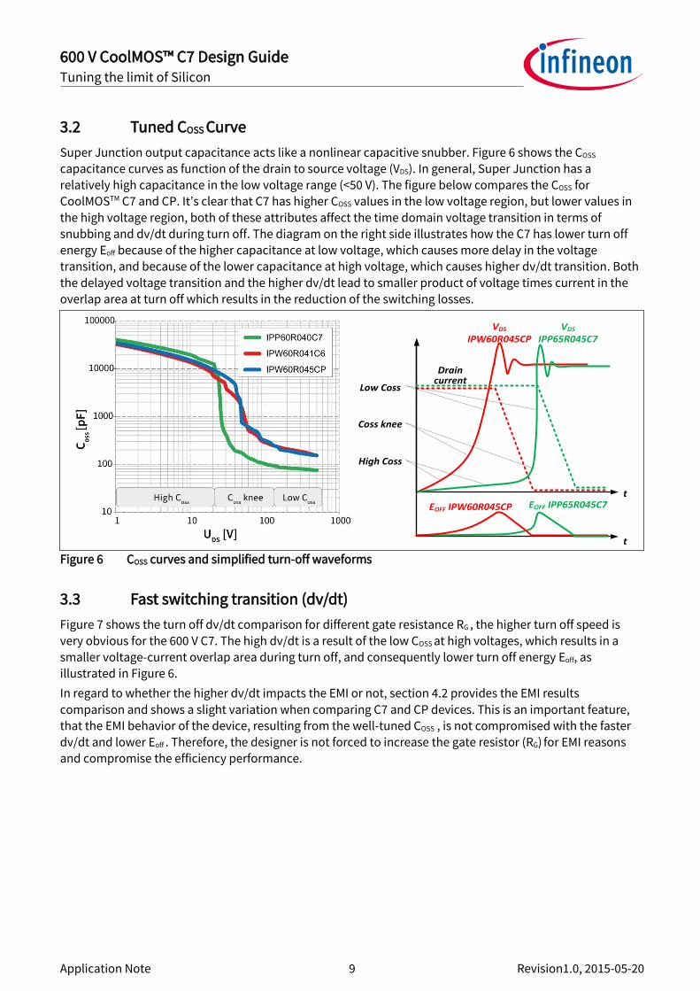
3.2 Tuned COSS Curve
Super Junction output capacitance acts like a nonlinear capacitive snubber. Figure 6 shows the COSS
capacitance curves as function of the drain to source voltage (VDS). In general, Super Junction has a relatively high capacitance in the low voltage range (<50 V). The figure below compares the COSS for CoolMOSTM C7 and CP. It’s clear that C7 has higher COSS values in the low voltage region, but lower values in
the high voltage region, both of these attributes affect the time domain voltage transition in terms of
snubbing and dv/dt during turn off. The diagram on the right side illustrates how the C7 has lower turn off energy Eoff because of the higher capacitance at low voltage, which causes more delay in the voltage transition, and because of the lower capacitance at high voltage, which causes higher dv/dt transition. Both
the delayed voltage transition and the higher dv/dt lead to smaller product of voltage times current in the overlap area at turn off which results in the reduction of the switching losses.
Figure 6 COSS curves and simplified turn-off waveforms
3.3 Fast switching transition (dv/dt)
Figure 7 shows the turn off dv/dt comparison for different gate resistance RG , the higher turn off speed is
very obvious for the 600 V C7. The high dv/dt is a result of the low COSS at high voltages, which results in a smaller voltage-current overlap area during turn off, and consequently lower turn off energy Eoff, as illustrated in Figure 6.
In regard to whether the higher dv/dt impacts the EMI or not, section 4.2 provides the EMI results
comparison and shows a slight variation when comparing C7 and CP devices. This is an important feature, that the EMI behavior of the device, resulting from the well-tuned COSS , is not compromised with the faster
dv/dt and lower Eoff . Therefore, the designer is not forced to increase the gate resistor (RG) for EMI reasons and compromise the efficiency performance.
High Coss
Low Coss
Coss knee
Drain current
VDS IPW60R045CP
VDS IPP65R045C7
EOFF IPP65R045C7EOFF IPW60R045CP
t
t

600 V CoolMOS™ C7 Design Guide Tuning the limit of Silicon
Application Note 10 Revision1.0, 2015-05-20
Design Note DN 2013-01
V1.0 January 2013
Figure 7 dv/dt comparision for 180-199 mΩ CoolMOS™ CP, 650 V C7 and 600 V C7
3.4 Low EOSS
As already discussed for the output capacitance (COSS), the capacitance drop of C7 takes place at lower
voltage levels compared to previous generations. This, combined with a remarkable reduction of the COSS level at high voltages, which dominates the overall value of the energy stored in the output capacitance,
brings the EOSS at typical DC link voltages of 400 V down to roughly one half of the previous generations, as is shown in Figure 8.
Figure 8 EOSS comparision for 40-45 mΩ and 180-199 mΩ of CoolMOS™ CP, 650 V C7 and 600 V C7
In hard switching applications, this energy is a fixed loss, EOSS is stored in the COSS during the turn-off phase; then is dissipated in the MOSFET channel in the next turn-on transient, as simplified in Figure 9.
0
5
10
15
20
25
30
35
0 100 200 300 400 500
Eo
ss
(µJ
]
UDS [V]
IPP60R040C7
IPP65R045C7
IPW60R045CP
0
1
2
3
4
5
6
7
8
0 100 200 300 400 500
Eo
ss
(µJ
]
UDS [V]
IPP60R180C7
IPP65R190C7
IPP60R199CP

600 V CoolMOS™ C7 Design Guide Tuning the limit of Silicon
Application Note 11 Revision1.0, 2015-05-20
Design Note DN 2013-01
V1.0 January 2013
Figure 9 Simplified EOSS dissipation mechanism in hard switching
This loss can be significant at light load condition because most of the other losses are load dependent and
decrease considerably at light load. Thus the EOSS reduction contributes to an improvement of the light load efficiency. Figure 10 illustrates the contribution of EOSS loss to the total MOSFET losses in a CCM PFC boost
application, showing that EOSS loss is two thirds of the total losses at 20% load condition.
Figure 10 EOSS contribution to total FET losses in PFC boost at different load conditions
In soft switching applications, with zero voltage turn on, this energy is recycled back to the circuit (before the turn-on) rather than dissipated, as simplified in Figure 11.
VCoss
ICoss
I II III IV V
iL
Vds
VGS
Coss
iL
+
-0V
iL
+
-0V→Vds
iL
+
-Vds
iL
+
-Vds→0V
iL
+
-0V
I II
Charging Coss
at turn off
III V
Coss Coss Coss Coss
IV
Dissipatting Coss energy
in the channel at turn on

600 V CoolMOS™ C7 Design Guide Tuning the limit of Silicon
Application Note 12 Revision1.0, 2015-05-20
Design Note DN 2013-01
V1.0 January 2013
Figure 11 Simplified EOSS recycling mechanism in soft switching
Although EOSS is assumed recycled in ZVS application, it is still desired to have lower EOSS. In topologies such
as resonant LLC or phase-shift Full Bridge, the designer must ensure proper sizing of the primary inductance
and its stores energy that is required to complete recycling of the EOSS and reach complete ZVS.
ZVS may be lost partially or completely if the inductive energy available in the circuit is not sufficient to charge and discharge the output capacitance of the two MOSFETs in the same bridge leg.
The Energy condition for achieving ZVS is:
𝐼𝑛𝑑𝑢𝑐𝑡𝑖𝑣𝑒 𝐸𝑛𝑒𝑟𝑔𝑦 ≥ 𝐶𝑎𝑝𝑎𝑐𝑖𝑡𝑖𝑣𝑒 𝐸𝑛𝑒𝑟𝑔𝑦
0.5 ∙ 𝐿𝑒𝑞 ∙ 𝐼𝐿 2 ≥ 0.5 ∙ (2 ∙ 𝐶o(er)) ∙ 𝑉𝑖𝑛
2
0.5 ∙ 𝐿𝑒𝑞 ∙ 𝐼𝐿 2 ≥ 2 ∙ 𝐸oss
where 𝐶o(er) is the MOSFET’s equivalent energy related output capacitance as listed in the datasheet. Figure
12 shows an example out of the IPP60R040C7 datasheet to show the 𝐶o(er) parameter and its definition,
which is used for energy calculation purposes.
Figure 12 Datasheet snapshot of the Co(er) capacitance and its difinition
Therefore, the tuned Coss curve of CoolMOSTM 600 V C7 resulting in lower Co(er) and EOSS , makes it easier for the designer to optimize efficiency without sacrificing ZVS. For example, in resonant LLC, the magnetizing inductance can be increased to reduce the lousy circulating primary side current, and in phase-shifted Full
Bridge, the ZVS will extend to a lighter load point, or the external primary side inductor used to increase the inductive energy might not be needed anymore.
VCoss
ICoss
I II III IV V
iL
Vds
VGS
iL
+
-0V
iL
+
-0V→Vds
iL
+
-Vds
iL
+
-Vds→0V
iL
+
-0V
I III
Coss Coss Coss Coss Coss
VII
Charging Coss
at turn off
IV
Recycling Coss energy
before turn on

600 V CoolMOS™ C7 Design Guide Tuning the limit of Silicon
Application Note 13 Revision1.0, 2015-05-20
Design Note DN 2013-01
V1.0 January 2013
3.5 Low QOSS
Due to the nonlinear capacitance of the Super Junction MOSFETs, the stored charge in the output
capacitance is mostly concentrated in the low voltage region. And due to the tuned COSS curve of the 600 V C7 CoolMOSTM, the integrated charge at the typical 400 V is reduced compared to other CoolMOSTM series, as shown in Figure 13.
Figure 13 QOSS comparision for 40-45 mΩ and 180-199 mΩ of CoolMOS™ CP, 650 V C7 and 600 V C7
The reduction in QOSS is advantageous in ZVS application as well, besides having sufficient energy for
achieving ZVS as discussed in the above section, the dead time between the two MOSFETs in the switching leg must also be long enough to allow the voltage transition.
The time condition for achieving ZVS is:
𝐷𝑒𝑎𝑑𝑡𝑖𝑚𝑒 ≥ 𝑍𝑉𝑆 𝑡𝑟𝑎𝑛𝑠𝑖𝑡𝑖𝑜𝑛 𝑡𝑖𝑚𝑒
𝐷𝑒𝑎𝑑𝑡𝑖𝑚𝑒 ≥ 2 ∗ 𝐶𝑜(𝑡𝑟) ∗𝑉𝐷𝑆
𝐼
𝐷𝑒𝑎𝑑𝑡𝑖𝑚𝑒 ≥ 2 ∗𝑄𝑂𝑆𝑆
𝐼
Where 𝐼 is the current used to charge and discharge both FETs in the switching leg.
𝑉𝐷𝑆 is the FET voltage, typically 400 V.
𝐶o(tr) is the MOSFET’s equivalent time related output capacitance as list in the datasheet. Figure 14 shows
the example from the IPP60R040C7 datasheet of the 𝐶o(tr) parameter and its definition, which is used for
time calculation purposes.
Figure 14 Datasheet snapshot of the Co(tr) capacitance and its difinition
Therefore, the QOSS and Co(tr) reduction facilitate completing the ZVS transition within the dead time period.
3.6 Low COSS dissipation factor
Every capacitor technology has a dissipation factor (tan∂=ESR*ωC) from which a practical capacitor has a series resistor ESR. Similarly, Super Junction MOSFETs also can be simply modeled with a series output resistance (ROSS), Figure 15, resulting in some dissipated energy during charging and discharging the COSS.
0
100
200
300
400
500
600
700
0 100 200 300 400 500
Qo
ss
[n
Q]
UDS [V]
IPP60R040C7
IPP65R045C7
IPW60R045CP
0
20
40
60
80
100
120
140
160
0 100 200 300 400 500
Qo
ss
[n
Q]
UDS [V]
IPP60R180C7
IPP65R190C7
IPP60R199CP

600 V CoolMOS™ C7 Design Guide Tuning the limit of Silicon
Application Note 14 Revision1.0, 2015-05-20
Design Note DN 2013-01
V1.0 January 2013
CoolMOS™ 600 V C7 series is optimized for low COSS energy dissipation. This is evident by the higher dv/dt shown in Figure 7, which can be explained by the efficient charging of the COSS , and by being less damped by
any structure impedance (ROSS).
Moreover, the energy dissipated in ROSS during charging and discharging COSS is a function of the passing
charge QOSS. Since CoolMOS™ 600 V C7 is featured with lowest QOSS in Figure 13, this results in a further reduction in COSS dissipated energy.
Figure 15 Schematic COSS circuit
This feature plays a significant role in soft switching applications, such as resonant LLC circuits, where in
theory the EOSS is completely recycled, while in reality, the inclusion of the COSS dissipation affects the
effectiveness of soft switching. Especially at high switching frequencies the COSS dissipation energy is important to be minimized, as it determines what portion of the EOSS is practically dissipated rather than recycled back as was assumed in Figure 11.
Figure 27 shows the efficiency comparison in a 600 W LLC circuit, the 0.1 % improvement across the load
range is mostly related to the low COSS dissipation, since other switching losses are minimal when operating at the resonant frequency.
3.7 Rugged body diode
The 600 V C7 CoolMOSTM body diode ruggedness was tested and proved a maximum dv/dt rating of 20 V/ns.
Furthermore its hard commutation was characterized in a double-pulse test fixture as shown in Figure 16.
The high side MOSFET is turned on to ramp the choke current to the specific value to be tested. When the high side MOSFET is turned off the choke current will freewheel through the body diode of the low side
MOSFET (DUT). After short freewheeling time the high side is turned on again causing the low side diode to hardly commutate the current and a negative reverse recovery current spike is seen in the diode current
waveform (LS_ISD), as in Figure 17.
Figure 16 Double pulse circuit for testing diode characteristics
Coss
Ross
LS_VDS
I_Choke
LS_ISD
DUT
Rg
Rg
600 V CoolMOS™ C7 Design Guide Tuning the limit of Silicon
Application Note 15 Revision1.0, 2015-05-20
Design Note DN 2013-01
V1.0 January 2013
Figure 17 Diode hard diode commutation waveform in a double pulse test circuit
The negative maximum reverse recovery current (Irrm), is one important parameter to characterize the hard commutation and the body diode robustness. For example, in the case of the 180 mΩ C7 part, Irrm=58 A was
seen to be a destruction limit for hard commutation, which can be reached either with a diode forward
current of 6A @ Rg=5 Ω, or with a 12 A @ Rg=30 Ω, as shown in Table 4.
Figure 18 shows the distruction wavefore for the 180 mΩ C7 part @Rg=30 Ω, where the body diode forward current is 12 A, and once hardly commutated the Irrm reached 58 A while dv/dt reaching 46 V/ns.
It must be noted that the results and destruction limits presented in this section are circuit and layout
specific. They will vary for different designs, and are only meant for relative comparison and understanding.
Table 4 Body diode reverse recovery destruction limits
Part # Body diode forward
current (A)
Gate resistor (Ω) Reverse recovery current
(Irrm) destruction limit (A)
IPx60R180C7 6 5
58 12 30
IPx60R040C7 34 8
110 8 30

600 V CoolMOS™ C7 Design Guide Tuning the limit of Silicon
Application Note 16 Revision1.0, 2015-05-20
Design Note DN 2013-01
V1.0 January 2013
Figure 18 Hard diode commutation failure waveform
3.7.1 When is rugged body diode needed?
In soft switching applications, such as resonant LLC and ZVS full-bridge converter, some circuit operations
may include hard commutation on the MOSFET’s body diode. In general, when a reverse current flows in the body diode, some charge (Qrr) is stored in the FET’s parasitic diode structure. If then the external voltage changes its direction, a high dv/dt voltage slope is applied to the diode before this charge is completely
removed. The residual charge will then be rushed out very quickly causing high di/dt current slope, hence causing high voltage overshoot.
Hard diode commutation can occur due to several circuit operations, such as:
1. Capacitive mode operation, Figure 19 shows the MOSFET operation in both inductive mode and in
capacitive mode. In the latter, the current is leading the voltage, and reverses it’s direction before the
half period has ended. The negative current flows in the body diode, when the next half period initiates by the turn on of the other MOSFET in the switching bridge. This exposes the diode to high dv/dt, and a high reverse recovery current spike is seen, as shown in Figure 19.
Figure 19 MOSFET operation in LLC circuit: Inductive mode (left), Capacitive mode (right)
MOSFET OFFDiode OFF
MOSFET OFFDiode ON
MOSFET ONDiode OFF
MOSFET OFFDiode OFF
IDS,L
VGS,L
VGS,H
MOSFET ONDiode OFF
MOSFET OFFDiode ON
MOSFET ONDiode OFF
MOSFET OFFDiode OFF
VDS,L
IDS,L
VGS,L
VGS,H
MOSFET ONDiode OFF
MOSFET OFFDiode Reverse Recovery

600 V CoolMOS™ C7 Design Guide Tuning the limit of Silicon
Application Note 17 Revision1.0, 2015-05-20
Design Note DN 2013-01
V1.0 January 2013
2. At light load or no load operation, hard commutation can occur in both LLC and ZVS full-bridge. When the diode conducts and stores Qrr charge during the dead time, the following period of the on-time is
supposed to generate a voltage drop across the diode. At light load this voltage drop can be insufficient to recover all the Qrr stored in the p-n region, hence the residual Qrr charge will cause hard commutation
of the body diode once the other bridge MOSFET is turned on, as can be seen in Figure 20.
Figure 20 MOSFET operation in light load
3. Also at short circuit, load transient and start-up, hard commutation can happen depending on the reaction speed of the control circuit. Although the steady state regulation curves were shaped to stay
away from the capacitive mode, these are transition modes that could force the operation to pass
through several cycles of capacitive mode and hard commutation, until the controller and resonant tank settle to the steady state again. Figure 21 is an illustration of the operational transition during short circuit, until detected and protected by the controller.
Figure 21 Short circuit operation in LLC circuit
3.8 Small area specific RDS(on)
Due to the technology break through, the latest CoolMOS™ C7 is available to offer the best performance among the CoolMOS™ family. It is able to provide a significant reduction of conduction and switching losses.
At the same time, the package limitation is further expanded. For the same packages the CoolMOS™ C7 technology offers lower possible on state resistance. As shown in Figure 22, the lowest RDS(on) of the TO-220
package is 40 mΩ which is 36% lower than for other technologies. The lowest RDS(on) in TO-247 is down to
17mΩ. Altogether it enables high power density and efficiency for the superior power conversion systems.
IDS,L
VGS,LVGS,H
td
Id,off
0.1 1 100
0.5
1
1.5
2
K .3 m, Fx, ( )
K 4 m, Fx, ( )
Fx
1
23
Gai
n
Normalize Frequency
Sho
rt c
ircu
it
Controller frequency increase protection
Normal inductive mode operation
Short circuit capacitve mode operation

600 V CoolMOS™ C7 Design Guide Tuning the limit of Silicon
Application Note 18 Revision1.0, 2015-05-20
Design Note DN 2013-01
V1.0 January 2013
Figure 22 Area specific RDS(on) comparison
Conventionally, the choice of package can be dominated by its thermal dissipation, which in some cases is the stopper from adopting smaller packages with smaller thermal interface area. But with the reduction of the total losses, such as in 600 V C7 CoolMOSTM, the thermal and mechanical designs can afford to use
smaller packages and maintain similar temperature performance at the same time.

600 V CoolMOS™ C7 Design Guide Tuning the limit of Silicon
Application Note 19 Revision1.0, 2015-05-20
Design Note DN 2013-01
V1.0 January 2013
3.9 TO-247 4pin package with Kelvin source connection
In common gate drive arrangements, the fast current transient causes a voltage drop VLS across the package
source inductance that can counteract the driving voltage. The induced source voltage, VLS = LS*di/dt, can reduce the gate current (Figure 23), therefore slowing down the switching transient and increasing the associated energy loss. In contrast to that, the Kelvin-source package concept is to exclude the package
source inductance and layout inductance from the driving loop, so that the LS*di/dt induced voltage is
outside the gate drive loop and does not affect the gate current anymore. So there is no increase of switching time and switching losses induced by the high di/dt on the drain to source power path.
Figure 23 a) Conventional package b) TO-247 4pin package
As the voltage spike accross the power source inductance is not incorporated in the gate drive circuit, the
quality of the gate signal increases at the same time. This helps to increase the robustness of the application as the stress to the driving circuit will be reduced. More detail to the advantages of TO-247 4pin package can
also be found inside its separate application note on the www.infineon.com/C7 homepage.

600 V CoolMOS™ C7 Design Guide Tuning the limit of Silicon
Application Note 20 Revision1.0, 2015-05-20
Design Note DN 2013-01
V1.0 January 2013
4 Experimental Results for CCM PFC and LLC
4.1 Efficiency comparison in standard CCM PFC (3pin vs. 4pin)
From the characterization data presented so far, it is clear that the 600 V C7 has substantially improved dynamic properties and can offer much lower RDS(on) in a given package. TO-220 package can now have RDS(on) as low as what was only available in the past in TO-247 package. The significance of this goes beyond space
utilization in the converter, as the TO-220 package has about one half of the source inductance of the TO-247. This offers even further performance potential for C7 over its predecessors due to better switching behavior and lower losses.
Moreover, 600 V C7 is also available with TO-247 4pin package which offers huge performance advantage for
the higher power range and enables the designer of SMPS to find very smart trade off optimization. More details of the high performance TO-247 4pin package can also be found inside its separate application note on the www.infineon.com/C7 homepage.
Figure 24 represents a comparison of the measured efficiency in a PFC between IPW60R045CP, IPP65R045C7, IPP60R040C7 and IPZ60R040C7, where the efficiency of IPW60R045CP is used as a normalized
reference and differences in % are plotted into the diagram. The maximum output power of this measurement is 1150 W where this on-state resistance class of MOSFETs is typically used.
Figure 24 Efficiency comparison between CoolMOSTM CP 3pin, 650 V C7 3pin, 600 V C7 3pin and 600 V C7
4pin.
Looking at the comparison of CP and C7, the technological differences mirrored in their key electrical
parameters (EOSS, QG and RDS(on)) are reflecting in the final efficiency test within the application. One can see the different aspects of improving the efficiency which is dominated by the lower switching losses at light load operation, whereas the slightly lower RDS(on) (40 mΩ vs. 45 mΩ) becomes more important towards heavy
load. Moreover, the 4pin package showed further efficiency improvement at heavy load due to improved
switching losses for high currents. Summing up the switching losses and RDS(on) advantages results in efficiency win for the whole load range even at the common switching frequencies of only 65 kHz. If the PFC uses higher switching frequencies, the advantage of the 600 V C7 will even be stronger pronounced.
0
0.1
0.2
0.3
0.4
0.5
0.6
0.7
0.8
0 200 400 600 800 1000 1200
Eff
icie
nc
y d
iffe
ren
ce
[%
]
Pout[W]
Efficiency difference for 90Vac (PFC CCM, 1150W @65kHz; RG=3Ohm)
IPP60R040C7IPP65R045C7IPW60R045CPIPZ60R040C7
fps@IFX
0,7% better efficiency@light load
0,5% better efficiency@full load

600 V CoolMOS™ C7 Design Guide Tuning the limit of Silicon
Application Note 21 Revision1.0, 2015-05-20
Design Note DN 2013-01
V1.0 January 2013
4.2 EMI comparison
EMI is a very important quality factor for a switching mode power supply. Especially the power switches are
the main source of the EMI noise based on their fast switching behaviour (high di/dt and dv/dt). The differential mode noise in the spectrum is induced by the PFC switching current and the circuit parameters. The common mode noise is caused by current induced by the high dv/dt in the switching with the parasitic
capacitors to the ground.
Figure 25 Conductive EMI of the PFC state with device IPW60R045CP(left) and IPW65R045C7 (right)
Figure 26 Conductive EMI of the PFC state with device IPW60R040C7
Due to the much faster dv/dt of the 600 V C7 device, the high frequency part of the common mode noise is
lightly higher than for 650 V C7 and 600 V CP devices. In the differential noise part there isn’t a significant
variation and the overall variation of the EMI noise spectrum is kept in a similar level. Out of this comparison one can see that the faster and more efficient switching of the 600 V CoolMOSTM C7 does not compromise in the EMI performance.
Av:35.66 Av:35.70
Av:35.04
Av:37.36 Av:35.26
Av:33.99
Av:37.97
Av:33.70
Av:35.1

600 V CoolMOS™ C7 Design Guide Tuning the limit of Silicon
Application Note 22 Revision1.0, 2015-05-20
Design Note DN 2013-01
V1.0 January 2013
The measurement is based on the ENRR022 standard. In the PFC state measurement, 600 V C7 meets both of the EMI average and quasi peak requirements. The design margin is more than 10 dB before touching the
standard line.
4.3 Efficiency comparison in resonant LLC half-bridge
Figure 27 shows the efficiency comparison in a 600W LLC circuit, Vin=380 V, Vo=12 V, running at resonant frequency fo=157 kHz. The 0.1 % improvement across the load range is mostly related to the low turn off losses and the low COSS dissipation, since other switching losses are minimal when operating at the resonant frequency. Furthermore, it’s expected to gain more efficiency benefit when operating above the resonant
frequency, where turn off losses start to engage.
Figure 27 Efficiency comparison in 600 W LLC half-bridge
-0.1
0.0
0.1
0.2
0.3
50 150 250 350 450 550 650
Effi
cie
ncy
dif
fere
nce
[%
]
Pout[W]
Delta Efficiency 600W LLC
with Deadtime Optimization_With Bias
IPP60R190P6
IPP60R180C7
600 V CoolMOS™ C7 Design Guide Tuning the limit of Silicon
Application Note 23 Revision1.0, 2015-05-20
Design Note DN 2013-01
V1.0 January 2013
5 Conclusions Infineon’s latest high-voltage super junction MOSFET technology 600 V CoolMOS™ C7 is able to achieve
typical RDS(on)*A values below 1 Ω*mm2 for the first time. Additionally, the switching FOMs are optimized to
keep both good ease-of-use and the best efficiency for hard and soft switching applications.
Furthermore, the relevance of the switching losses at high currents (i.e. power ratings) makes CoolMOS™ C7 an enabler for higher frequencies and/or higher power ratings.
The 600 V CoolMOSTM C7 is the next step of silicon improvement based on the 650 V CoolMOS™ C7. It stays
with the strategy to increase the switching performance in order to enable highest efficiency in all of the
target applications as for example in boost topologies like power factor correction and high voltage DC/DC
stages like LLC’s (DC/DC stage with resonant tank in order to maintain zero voltage switching). Although the
600 V CoolMOS™ C7 offers very fast switching, it also retains the ease of use level (how easy to control the
switch) of the 650 V C7 “parent technology”. Therefore, 600 V CoolMOSTM C7 is the optimized device for highest efficiency switched mode power supply.
In combination with the innovative TO-247 4pin package the 600 V C7 represents the new standard of SJ
MOSFET.

600 V CoolMOS™ C7 Design Guide Tuning the limit of Silicon
Application Note 24 Revision1.0, 2015-05-20
Design Note DN 2013-01
V1.0 January 2013
6 List of abbreviations
CGD ...................................................................................................... internal gate drain capacitance CGD=Crss
Ciss ................................................................................................................ input capacitance Ciss=CGS+CGD
Co(er) ...................................................................................................................... effective output capacitance
di/dt ............................................................................... steepness of current comutation at turn off / turn on
DUT .......................................................................................................................................... device under test
dv/dt .............................................................................. steepness of voltage comutation at turn off / turn on
Eoff .......................................................................................................................... power loss during switch off
Eon .......................................................................................................................... power loss during switch on
Eoss ..................................................................... stored energy in output capacitance (Coss) at typ. VDS=400V
FOM............................................................................................................................................ Figures of Merit
ID .................................................................................................................................................... drain current
MOSFET ............................................................................... metal oxide semiconductor field effect transistor
PFC................................................................................................................................ power factor correction
PNP .......................................................................................................... bipolar transistor type (pnp vs. npn)
QOSS ............................................................................................................................ Chage stored in the COSS
RDS(on) ............................................................................................................... drain-source on-state resistance
SMPS .................................................................................................................... switched mode power supply
VDS .......................................................................................... drain to source voltage, drain to source voltage
ZVS .................................................................................................................................. zero voltage switching
QG………………………………………………………………………………………………………..Gate Charge
QGS……………………………………………………………………………………..Gate Charge, gate to source
QGD……………………………………………………………………………………….Gate Charge, gate to drain
RG………………………………………………………………………………………………………...Gate resistor
CCM PFC………………………………………………….Continous conduction mode power factor correction
LS………………………………………………………………….………………..……………..Source inductance
LLC…………………………….. DC/DC stage with resonant tank in order to maintain zero voltage switching
600 V CoolMOS™ C7 Design Guide Tuning the limit of Silicon
Application Note 25 Revision1.0, 2015-05-20
Design Note DN 2013-01
V1.0 January 2013
7 Usefull material and links
600 V CoolMOS™ C7 Webpage
www.infineon.com/600V-C7
650 V CoolMOS™ C7 Webpage
www.infineon.com/c7
CoolMOS™ CP
www.infineon.com/cp
600 V CoolMOS™ C7 Design Guide Tuning the limit of Silicon
Application Note 26 Revision1.0, 2015-05-20
Design Note DN 2013-01
V1.0 January 2013
8 References [1] X. B. Chen and C. Hu, Optimum doping profile of power MOSFET’s epitaxial Layer. IEEE Trans.Electron
Devices, vol. ED-29, pp. 985-987, 1982.
[2] T. Fujihira: “Theory of Semiconductor superjunction Devices”, Jpn.J.Appl.Phys., Vol. 36, pp. 6254-6262, 1997.
[3] Deboy, G., März, M., Stengl, J. Strack, H., Tihanyi, J. and Wever, H., A New Generation of High Voltage
MOSFETs Breaks the Limit of Silicon. Proc. IEDM 98, San Francisco, Calif., December 1998, pp. 26.2.1- 26.2.3.
[4] G. Deboy, F. Dahlquist, T. Reimann and M. Scherf: Latest Generation of superjunction Power MOSFETs
Permits the use of Hard-switching Topologies for High Power Applications. Proceedings of PCIM
Nürnberg, 2005, pp. 38-40.
[5] Hancock, J. M.: Advancing Performance in HV Semiconductors Enables Hard Switching Topologies,
Proceedings of Power Electronics Technology Conference, October 2005, on CD-ROM.
[6] F. Stueckler, E. Vecino, Infineon Technologies Application Note: “Coo lMOSTM C7 650V Switch in a
Kelvin Source Configuration”. May 2013.
http://www.infineon.com/dgdl/Infineon+-+Application+Note+-+TO-247-4pin+-+650V+CoolMOS™
+C7+Switch+in+a+Kelvin+Source+Configuration.pdf?folderId=db3a304333b8a7ca0133c6bec0956188&fileId=db3a30433e5a5024013e6a9908a26410
[7] J. Hancock, F. Stueckler, E. Vecino, Infineon Technologies Application Note: “CoolMOS™ C7 : Mastering
the Art of Quickness”. April 2013.
http://www.infineon.com/dgdl/Infineon+-+Application+Note+-+650V+CoolMOS™ +C7+-
+Mastering+the+Art+of+Quickness.pdf?folderId=db3a304333b8a7ca0133c6bec0956188&fileId=db3a30
433e5a5024013e6a966779640b
[8] S. Abdel-Rahman, F. Stueckler, K. Siu, Infineon Technologies Application Note: “PFC Boost Converter
Design Guide. November 2014.
http://www.infineon.com/dgdl/Infineon-ApplicationNote_PFCCCMBoostConverterDesignGuide-AN-
v02_00-EN.pdf?fileId=5546d4624a56eed8014a62c75a923b05

600 V CoolMOS™ C7 Design Guide Tuning the limit of Silicon
Application Note 27 Revision1.0, 2015-05-20
Design Note DN 2013-01
V1.0 January 2013
Revision History
Major changes since the last revision
Page or Reference Description of change
-- First Release

Published by
Infineon Technologies AG
81726 Munich, Germany
© 2015 Infineon Technologies AG. All Rights Reserved.
Do you have a question about any
aspect of this document?
Email: [email protected]
Document reference
Legal Disclaimer THE INFORMATION GIVEN IN THIS APPLICATION NOTE (INCLUDING BUT NOT LIMITED TO CONTENTS OF REFERENCED WEBSITES) IS GIVEN AS A HINT FOR THE IMPLEMENTATION OF THE INFINEON TECHNOLOGIES COMPONENT ONLY AND SHALL NOT BE REGARDED AS ANY DESCRIPTION OR WARRANTY OF A CERTAIN FUNCTIONALITY, CONDITION OR QUALITY OF THE INFINEON TECHNOLOGIES COMPONENT. THE RECIPIENT OF THIS APPLICATION NOTE MUST VERIFY ANY FUNCTION DESCRIBED HEREIN IN THE REAL APPLICATION. INFINEON TECHNOLOGIES HEREBY DISCLAIMS ANY AND ALL WARRANTIES AND LIABILITIES OF ANY KIND (INCLUDING WITHOUT LIMITATION WARRANTIES OF NON-INFRINGEMENT OF INTELLECTUAL PROPERTY RIGHTS OF ANY THIRD PARTY) WITH RESPECT TO ANY AND ALL INFORMATION GIVEN IN THIS APPLICATION NOTE.
Information For further information on technology, delivery terms and conditions and prices, please contact the nearest Infineon Technologies Office (www.infineon.com).
Warnings Due to technical requirements, components may contain dangerous substances. For information on the types in question, please contact the nearest Infineon Technologies Office. Infineon Technologies components may be used in life-support devices or systems only with the express written approval of Infineon Technologies, if a failure of such components can reasonably be expected to cause the failure of that life-support device or system or to affect the safety or effectiveness of that device or system. Life support devices or systems are intended to be implanted in the human body or to support and/or maintain and sustain and/or protect human life. If they fail, it is reasonable to assume that the health of the user or other persons may be endangered.
www.infineon.com
Trademarks of Infineon Technologies AG AURIX™, C166™, CanPAK™, CIPOS™, CIPURSE™, CoolGaN™, CoolMOS™, CoolSET™, CoolSiC™, CORECONTROL™, CROSSAVE™, DAVE™, DI-POL™, DrBLADE™, EasyPIM™, EconoBRIDGE™, EconoDUAL™, EconoPACK™, EconoPIM™, EiceDRIVER™, eupec™, FCOS™, HITFET™, HybridPACK™, ISOFACE™, IsoPACK™, i-Wafer™, MIPAQ™, ModSTACK™, my-d™, NovalithIC™, OmniTune™, OPTIGA™, OptiMOS™, ORIGA™, POWERCODE™, PRIMARION™, PrimePACK™, PrimeSTACK™, PROFET™, PRO-SIL™, RASIC™, REAL3™, ReverSave™, SatRIC™, SIEGET™, SIPMOS™, SmartLEWIS™, SOLID FLASH™, SPOC™, TEMPFET™, thinQ!™, TRENCHSTOP™, TriCore™.
Other Trademarks Advance Design System™ (ADS) of Agilent Technologies, AMBA™, ARM™, MULTI-ICE™, KEIL™, PRIMECELL™, REALVIEW™, THUMB™, µVision™ of ARM Limited, UK. ANSI™ of American National Standards Institute. AUTOSAR™ of AUTOSAR development partnership. Bluetooth™ of Bluetooth SIG Inc. CAT-iq™ of DECT Forum. COLOSSUS™, FirstGPS™ of Trimble Navigation Ltd. EMV™ of EMVCo, LLC (Visa Holdings Inc.). EPCOS™ of Epcos AG. FLEXGO™ of Microsoft Corporation. HYPERTERMINAL™ of Hilgraeve Incorporated. MCS™ of Intel Corp. IEC™ of Commission Electrotechnique Internationale. IrDA™ of Infrared Data Association Corporation. ISO™ of INTERNATIONAL ORGANIZATION FOR STANDARDIZATION. MATLAB™ of MathWorks, Inc. MAXIM™ of Maxim Integrated Products, Inc. MICROTEC™, NUCLEUS™ of Mentor Graphics Corporation. MIPI™ of MIPI Alliance, Inc. MIPS™ of MIPS Technologies, Inc., USA. muRata™ of MURATA MANUFACTURING CO., MICROWAVE OFFICE™ (MWO) of Applied Wave Research Inc., OmniVision™ of OmniVision Technologies, Inc. Openwave™ of Openwave Systems Inc. RED HAT™ of Red Hat, Inc. RFMD™ of RF Micro Devices, Inc. SIRIUS™ of Sirius Satellite Radio Inc. SOLARIS™ of Sun Microsystems, Inc. SPANSION™ of Spansion LLC Ltd. Symbian™ of Symbian Software Limited. TAIYO YUDEN™ of Taiyo Yuden Co. TEAKLITE™ of CEVA, Inc. TEKTRONIX™ of Tektronix Inc. TOKO™ of TOKO KABUSHIKI KAISHA TA. UNIX™ of X/Open Company Limited. VERILOG™, PALLADIUM™ of Cadence Design Systems, Inc. VLYNQ™ of Texas Instruments Incorporated. VXWORKS™, WIND RIVER™ of WIND RIVER SYSTEMS, INC. ZETEX™ of Diodes Zetex Limited. Last Trademarks Update 2014-07-17
Edition 2015-05-01
AN_201411_PL52_005