55:131 introduction to vlsi design
TRANSCRIPT

55:131 Introduction to VLSI Design
Implementation Options Adapted from Weste and Harris notes

Implementation Options Use an existing chip Field Programmable Gate Array Sea of Gates/Gate Array Standard Cell Full Custom
2 55:131 Introduction to VLSI Design

Implementation Options Use an existing chip
Pros Minimal hardware development cost – hardware is “done”!
Cons May need a (big) software development! Other features may not be a great fit Beware of performance limitations Beware of power consumption Don’t forget about other hardware (memories, PHYs, etc)
Examples Off-the-shelf microprocessor Application Specific device
3 55:131 Introduction to VLSI Design

Applied Micro PPC460EX
Courtesy of Applied Micro (APM) 4 55:131 Introduction to VLSI Design

Implementation Options FPGAs or PLDs
Pros Back-end (fabrication) is done
Saves time and money Cons
Clock rate usually won’t match that of a Gate Array/Std Cell Usually has higher recurring cost “Fixed” feature set (RAM, PLLs, etc) may limit your options
Examples RAM-based FPGA from Xilinx or Altera Flash-based FPGA from Actel
5 55:131 Introduction to VLSI Design

Simplified FPGA Floorplan
6 55:131 Introduction to VLSI Design

“Configured” FPGA
7 55:131 Introduction to VLSI Design

Xilinx CLB – a.k.a. “Slice”
8 55:131 Introduction to VLSI Design

4-input Look-up Table Implementation
Out = f (in0, in1, in2, in3)
In0 In1 In2 In3
Out
…
16 SRAM Cells
9 55:131 Introduction to VLSI Design

Implementation Options Sea of Gates/Gate Array
Pros Much of the fabrication is done
Base wafers have transistors and memories done “User”-defined logic implemented in (a few) metal layers
Lower development costs than Standard Cell because supplier can amortize mask costs over all base array designs
Better clock rate and lower power than FPGA Cons
Clock rate usually won’t match that of a Std Cell “Fixed” feature set (RAM, PLLs, etc) may limit your options
Examples LSI Logic LCA500K
10 55:131 Introduction to VLSI Design

Simplified Sea of Gates Floorplan
11 55:131 Introduction to VLSI Design

SoG and Gate Array Cell Layouts
12 55:131 Introduction to VLSI Design

SoG and Gate Array 3-in NAND
13 55:131 Introduction to VLSI Design

Implementation Options Standard Cell
Pros Smaller, faster, lower power than FPGA or SoG/GA Faster development time than full custom because a standard
cell library is used as the basic building blocks of the design Cons
Custom mask set is expensive Resistance to add library elements Economical only for
High volume or High cost devices
Examples AMIS SC13 standard cell
14 55:131 Introduction to VLSI Design

Standard Cell Layout
15 55:131 Introduction to VLSI Design

Standard Cell Library Example
16 55:131 Introduction to VLSI Design
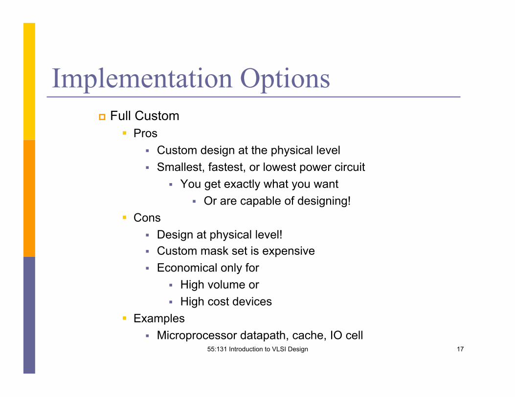
Implementation Options Full Custom
Pros Custom design at the physical level Smallest, fastest, or lowest power circuit
You get exactly what you want Or are capable of designing!
Cons Design at physical level! Custom mask set is expensive Economical only for
High volume or High cost devices
Examples Microprocessor datapath, cache, IO cell
55:131 Introduction to VLSI Design 17

Custom Design Flow
18 55:131 Introduction to VLSI Design

CMOS Design Methods
19 55:131 Introduction to VLSI Design