5 flexible power ampliier architectures for spectrum eficient
TRANSCRIPT

Flexible Power Ampliier Architectures for Spectrum Eficient Wireless Applications 73
Flexible Power Ampliier Architectures for Spectrum Eficient Wireless Applications
Alessandro Cidronali, Iacopo Magrini and Gianfranco Manes
x
Flexible Power Amplifier Architectures for Spectrum Efficient Wireless Applications
Alessandro Cidronali, Iacopo Magrini and Gianfranco Manes
Department of Electronics and Telecommunications, University of Firenze, Italy
1. Introduction
The wireless systems evolution known as “beyond the 3rd generation” (B3G) will make use of dynamic spectrum access techniques to provide wide bandwidth to mobile users via heterogeneous wireless networks. A consistent step toward this scenario is represented by the outcome of the last World Radiocommunication Conference [1] which established new primary frequency bands allocation spanning from the UHF band to low microwaves and thus reflecting the increasing demands for broadband mobile and cellular systems. We have become used to the doubling of processing power of chips based on Moore’s law, but the progress in radio interface technologies still poses significant challenges. High spectrum efficiency performance becomes therefore another major requirement of the design, along with the more consolidated ones: energy efficiency, integration, cost and reliability. While the IMT-advanced roadmap foresees a 100 Mbps data rate for mobile users and a peak of 1 Gbps is expected for nomadic users, the available spectrum for legacy wireless communications is fragmented and reaches the amount of 750 MHz in the S-C band. A radio technology that is expected to interact with a multi-services network should be able to change between different operating bands and adapt its features according with the different available standard and requirements. Most of the research efforts performed during the last years dealt with issues related to the physical layer of the communication stack [2]; however, despite the growing interest in multi-standard operation, less attention has been devoted to the radio-frequency front-end, which therefore remains one of the most challenging parts of a multi-band radio. One main reason for the delay in effectively implementing multi-standard transceivers can be attributed to the implementation of the RF transmit power amplifier (PA). Today, dedicated, single standard PAs achieve very good power added efficiency (PAE) and, in this way, long battery lifetime. Any multi-standard PA, needed for the support of different, not always predefined, communication systems, should compete with such dedicated solutions. A conceptual framework to this is provided by the so-called software-defined radio (SDR), i.e. a radio communication system, using software for the reconfiguration of the digital and analog parts in order to perform the modulation and demodulation of radio signals, [3]. In practice, however, due to the difficulty of implementing the fast signal processing implied in the SDR approach, most of
5
www.intechopen.com
Advanced Microwave Circuits and Systems74
the systems on the market, based on more traditional approaches, are still supporting only a very limited number of standards (e.g. 4 GSM frequencies, UMTS and, possibly, Bluetooth). In the near future, further standards will have to be supported, and more could have to be added during the handset lifetime, hopefully without hardware reconfiguration. This will determine the need of multiband PAs capable to transmit efficiently more than one service with variable radio access schemes. Example of realizations in different technologies are provided in this Chapter as demonstrators of the discussed multiband design methods. The flexibility of the operative frequency is thus introduced by analyzing new PA architectures and design methodologies which consider the inclusion of tunable and switching components to enable a change in the operative frequency. A review of the most promising circuit topologies suitable to design reconfigurable matching networks is given in this Chapter. Varactor diodes based and MOS switched based topologies are compared, highlighting their point of strength and weakness. It is shown as a concurrent dual-band PA implemented by the proper combination of frequency-dedicated PAs, each of them optimized to work in a given bandwidth would be an easy approach, it becomes unsuited due to the complexity of the power combiners. For this reason the true concurrent dual band PA presented in this chapter is to be considered as an enabler components for high efficiency multiband systems. Spectrum efficiency is just one of the challenges a wireless system designer faces, further come from linearity and energy efficiency resulting from the use of multicarrier and complex envelope modulation schemes. As the spectrum efficiency increases a more demanding requirement in term of PA linearity faces to the designers. Energy efficiency and linearity are conventionally traded-off considering that increasing the power back-off increases the linearity at the expenses of lower energy efficiency. To maintain signal integrity, the resulting waveforms in turn require linear transmission paths for their successful deployment. A way to match signal integrity and energy efficiency consists in the use of digital predistortion algorithm applied at base-band and implemented in the digital section of the transmitter. In spite of their large development in frequency dedicated PA architectures, the development of a technique suitable for multi-band applications is not yet completely available. In this Chapter a comprehensive treatment a novel technique for Dual Band Digital Predistortion (DB-DP) is discussed. The DB-PD is based on the simultaneous predistortion of both channels at intermediate frequency (IF), it uses a single band memory polynomial DP for linearization, while the feedback path is based on a subsampling receiver. The memory polynomial DB-DP system is presented by simulation with Matlab-Simulink® for a deep understanding of performance.
2. A possible applicative scenario for multi-band transmitters
Extending the scenario to already experienced 3G voice/data systems, users may be moving while simultaneously operating in a broadband data access or multimedia streaming session. The need to support low latency and low packet loss handovers of data streams as users transition from one access point to another may require the concurrent use of more than one frequency band at the time. For full-mobile data services, no user interaction will be required to adapt their service expectations because of environmental limitations that are technically challenging but not directly relevant to the user (such as being stationary or moving). The enabling front-end of future mobile unit thus will accommodate more than
one system in a effective and efficient way to make possible the connectivity capabilities depicted in Fig. 1.
Fig. 1. Concept of a multi-band transmitter The Wireless Local Area Network (WLAN) industry has become one of the fastest growing segments of the communications industry. This growth is due, in large part, to the introduction of standards-based WLAN products, regulated by the IEEE 802.11. The expectation of the WLAN’s continuing growth stems from the promise of new standardized WLAN technologies, from improved cost/performance of WLAN systems, and from the growing availability of WLAN solutions that consolidate voice, data, and mobility functions. This, combined with market forecasts reporting that WLAN will experience a continuous growth in the next years, show that WLAN technologies will play a significant role in the future and will have a significant impact on our business and personal life styles. The WiMAX is an alternative and complementing standard for high data rate transmission, which will transform the world of mobile broadband by enabling the cost-effective deployment of metropolitan area networks based on the IEEE 802.16 standard to support notebook PC and mobile users on move. There are many advantages of systems based on 802.16, e.g. the ability to provide service even in areas that are difficult for wired infrastructure to reach and the ability to overcome the physical limitations of traditional wired infrastructure. The standard will offer wireless connectivity of up to 30 miles. The major capabilities of the standard are its widespread reach, which can be used to set up a metropolitan area network, and its data capacity of 75 Mbps. This high-speed wireless broadband technology promises to open new, economically viable market opportunities for operators, wireless Internet service providers and equipment manufacturers. The flexibility of wireless technology, combined with high throughput, scalability and long-range features of the IEEE 802.16 standard helps to fill the broadband coverage gaps and reach millions of new residential and business customers worldwide. With WLAN 802.11 and now WiMAX 802.16, there has been a growing interest in technologies that allow delivery of higher data rates over large geographical areas. The IEEE 802.16 family of standards (802.16-2004 and 802.16e) are intended to provide high
www.intechopen.com

Flexible Power Ampliier Architectures for Spectrum Eficient Wireless Applications 75
the systems on the market, based on more traditional approaches, are still supporting only a very limited number of standards (e.g. 4 GSM frequencies, UMTS and, possibly, Bluetooth). In the near future, further standards will have to be supported, and more could have to be added during the handset lifetime, hopefully without hardware reconfiguration. This will determine the need of multiband PAs capable to transmit efficiently more than one service with variable radio access schemes. Example of realizations in different technologies are provided in this Chapter as demonstrators of the discussed multiband design methods. The flexibility of the operative frequency is thus introduced by analyzing new PA architectures and design methodologies which consider the inclusion of tunable and switching components to enable a change in the operative frequency. A review of the most promising circuit topologies suitable to design reconfigurable matching networks is given in this Chapter. Varactor diodes based and MOS switched based topologies are compared, highlighting their point of strength and weakness. It is shown as a concurrent dual-band PA implemented by the proper combination of frequency-dedicated PAs, each of them optimized to work in a given bandwidth would be an easy approach, it becomes unsuited due to the complexity of the power combiners. For this reason the true concurrent dual band PA presented in this chapter is to be considered as an enabler components for high efficiency multiband systems. Spectrum efficiency is just one of the challenges a wireless system designer faces, further come from linearity and energy efficiency resulting from the use of multicarrier and complex envelope modulation schemes. As the spectrum efficiency increases a more demanding requirement in term of PA linearity faces to the designers. Energy efficiency and linearity are conventionally traded-off considering that increasing the power back-off increases the linearity at the expenses of lower energy efficiency. To maintain signal integrity, the resulting waveforms in turn require linear transmission paths for their successful deployment. A way to match signal integrity and energy efficiency consists in the use of digital predistortion algorithm applied at base-band and implemented in the digital section of the transmitter. In spite of their large development in frequency dedicated PA architectures, the development of a technique suitable for multi-band applications is not yet completely available. In this Chapter a comprehensive treatment a novel technique for Dual Band Digital Predistortion (DB-DP) is discussed. The DB-PD is based on the simultaneous predistortion of both channels at intermediate frequency (IF), it uses a single band memory polynomial DP for linearization, while the feedback path is based on a subsampling receiver. The memory polynomial DB-DP system is presented by simulation with Matlab-Simulink® for a deep understanding of performance.
2. A possible applicative scenario for multi-band transmitters
Extending the scenario to already experienced 3G voice/data systems, users may be moving while simultaneously operating in a broadband data access or multimedia streaming session. The need to support low latency and low packet loss handovers of data streams as users transition from one access point to another may require the concurrent use of more than one frequency band at the time. For full-mobile data services, no user interaction will be required to adapt their service expectations because of environmental limitations that are technically challenging but not directly relevant to the user (such as being stationary or moving). The enabling front-end of future mobile unit thus will accommodate more than
one system in a effective and efficient way to make possible the connectivity capabilities depicted in Fig. 1.
Fig. 1. Concept of a multi-band transmitter The Wireless Local Area Network (WLAN) industry has become one of the fastest growing segments of the communications industry. This growth is due, in large part, to the introduction of standards-based WLAN products, regulated by the IEEE 802.11. The expectation of the WLAN’s continuing growth stems from the promise of new standardized WLAN technologies, from improved cost/performance of WLAN systems, and from the growing availability of WLAN solutions that consolidate voice, data, and mobility functions. This, combined with market forecasts reporting that WLAN will experience a continuous growth in the next years, show that WLAN technologies will play a significant role in the future and will have a significant impact on our business and personal life styles. The WiMAX is an alternative and complementing standard for high data rate transmission, which will transform the world of mobile broadband by enabling the cost-effective deployment of metropolitan area networks based on the IEEE 802.16 standard to support notebook PC and mobile users on move. There are many advantages of systems based on 802.16, e.g. the ability to provide service even in areas that are difficult for wired infrastructure to reach and the ability to overcome the physical limitations of traditional wired infrastructure. The standard will offer wireless connectivity of up to 30 miles. The major capabilities of the standard are its widespread reach, which can be used to set up a metropolitan area network, and its data capacity of 75 Mbps. This high-speed wireless broadband technology promises to open new, economically viable market opportunities for operators, wireless Internet service providers and equipment manufacturers. The flexibility of wireless technology, combined with high throughput, scalability and long-range features of the IEEE 802.16 standard helps to fill the broadband coverage gaps and reach millions of new residential and business customers worldwide. With WLAN 802.11 and now WiMAX 802.16, there has been a growing interest in technologies that allow delivery of higher data rates over large geographical areas. The IEEE 802.16 family of standards (802.16-2004 and 802.16e) are intended to provide high
www.intechopen.com

Advanced Microwave Circuits and Systems76
bandwidth wireless voice and data for residential and enterprise use. The modulation used to achieve these high data rates is orthogonal frequency-division multiplexing (OFDM). WiMAX OFDM features a minimum of 256 subcarriers up to 2048 subcarriers, each modulated with either BPSK, QPSK, 16 QAM or 64 QAM modulation. Having these carriers orthogonal to each other minimizes self-interference. This standard also supports different signal bandwidths, from 1.25 MHz to 20 MHz to facilitate transmission over longer ranges and to accommodate different multipath environments. This represents a significant increase in system profile complexity as compared to the 802.11 standard, mostly to guarantee a wider, more efficient, more robust network. More subcarriers and variable-length guard intervals contribute to this enhancement. The ability to develop and manufacture a single reconfigurable terminal, which can be configured at the final stage of manufacture to tailor it to a particular market, clearly presents immense benefits to equipment manufacturers. With the design, components used, and hardware manufacturing processes all being identical for all terminals worldwide, the economy of scale would be huge. This has the potential to offset the additional hardware costs which would be inevitable in the realisation of such a generic device. Based on this, the scenario adopted reflects in the request for transceiver architectures capable to support cellular phone, WLAN and WiMAX in an ’always and everywhere connected’ solution. The transceiver performance in this multi-standard operation, however, comes at the expense of RF specifications that are more difficult to achieve. Furthermore, the choice and definition of the proper transceiver architecture becomes a difficult task, since several parameters - as now imposed by two standards - must be taken into account.
3. Suitable architectures for multiband-multimode transmitters
The concept of a multiband or general coverage terminal is, strictly speaking, an extension of the basic SDR concept into that of a broadband flexible architecture radio, since the basic reconfigurability and adaptability aspects of operation do not depend upon multiband coverage. It would be possible, for example, to construct a useful SDR which operated in the 800-900 MHz area of spectrum and which could adapt between AMPS, GSM, DAMPS, PDC, and CDMA. It is now normal, however, for a handset to have multi-frequency operation and hence the extension of this principle to a SDR is a natural one. The international business traveler market is still seen as both large and lucrative, particularly in terms of call charges, hence making this type of handset attractive to both manufacturers and network providers. An ideal SDR is shown in Fig. 2; note that the A/D converter is assumed to have a built-in anti-alias filter and that the D/A is assumed to have a built-in reconstruction filter. The ideal software defined radio has the following features [4]:
The radio access scheme (i.e. modulation scheme, channelization, coding) and equalization for transmitter and receiver are all determined in software within the digital processing subsystem. This is shown containing a DSP in Fig. 2
The ideal circulator is used to separate the transmit and receive path signals, without the usual frequency restrictions placed upon this function when using filter-based solutions (e.g., a conventional diplexer). This component relies on ideal matching between itself and the antenna and power amplifier impedances and so is unrealistic in practice over a broad frequency band. Since the primary
alternative, a diplexer, is very much a frequency-dedicated component, its elimination is a key element in a multiband or even multimode transceiver.
The linear, or linearised, PA ensures an ideal transfer of the RF modulation from the DAC to a high-power signal suitable for transmission, with ideally no adjacent channel emissions. Note that this function could also be provided by an RF synthesis technique, in which case the DAC and power amplifier functions would effectively be combined into a single high-power RF synthesis block.
Anti-alias and reconstruction filtering is clearly required in this architecture (not shown in Fig. 2
. It should, however, be relatively straightforward to implement, assuming that the ADC and DAC have sampling rates of many gigahertz. Current transmit, receive, and duplex filtering can achieve excellent roll-off rates in both handportable and (especially) base-station designs. The main change would be in transforming them from bandpass (where relevant) to lowpass designs.
Fig. 2. Ideal software defined radio architecture Possibly the most important element of any SDR system, whether in a base station or handset, is the linear or linearised multiband transmitter. Receiver systems have always required a high degree of linearity, as they must possess a good signal handling capability, in addition to good low-noise performance. In the case of transmitters, however, a high degree of linearity is a relatively recent requirement, arising predominantly from the widespread adoption of multi symbols envelope-varying digital modulations. This follows from the fact that most modern modulation formats incorporate some degree of envelope variation, the only significant exception at present being GSM and its derivatives (DCS and PCS). The basic architecture of a SDR transmitter revolves around the creation of a baseband version of the desired RF spectrum, followed by a linear path translating that spectrum to a high-power RF signal. Nevertheless the implementation of a true SDR poses a further very critical issues, i.e. the power consumption of the analogue-digital converter. Let’s consider for instance the use of a flash converter, largely available in the market with a maximum number of bit about 18 preceded by a sample and hold circuit. Carrying out a simplified calculation, given the converter dynamic range, Dc, the power consumption of this systems is:
1010Dc
dcs
kTPt
, (1)
www.intechopen.com

Flexible Power Ampliier Architectures for Spectrum Eficient Wireless Applications 77
bandwidth wireless voice and data for residential and enterprise use. The modulation used to achieve these high data rates is orthogonal frequency-division multiplexing (OFDM). WiMAX OFDM features a minimum of 256 subcarriers up to 2048 subcarriers, each modulated with either BPSK, QPSK, 16 QAM or 64 QAM modulation. Having these carriers orthogonal to each other minimizes self-interference. This standard also supports different signal bandwidths, from 1.25 MHz to 20 MHz to facilitate transmission over longer ranges and to accommodate different multipath environments. This represents a significant increase in system profile complexity as compared to the 802.11 standard, mostly to guarantee a wider, more efficient, more robust network. More subcarriers and variable-length guard intervals contribute to this enhancement. The ability to develop and manufacture a single reconfigurable terminal, which can be configured at the final stage of manufacture to tailor it to a particular market, clearly presents immense benefits to equipment manufacturers. With the design, components used, and hardware manufacturing processes all being identical for all terminals worldwide, the economy of scale would be huge. This has the potential to offset the additional hardware costs which would be inevitable in the realisation of such a generic device. Based on this, the scenario adopted reflects in the request for transceiver architectures capable to support cellular phone, WLAN and WiMAX in an ’always and everywhere connected’ solution. The transceiver performance in this multi-standard operation, however, comes at the expense of RF specifications that are more difficult to achieve. Furthermore, the choice and definition of the proper transceiver architecture becomes a difficult task, since several parameters - as now imposed by two standards - must be taken into account.
3. Suitable architectures for multiband-multimode transmitters
The concept of a multiband or general coverage terminal is, strictly speaking, an extension of the basic SDR concept into that of a broadband flexible architecture radio, since the basic reconfigurability and adaptability aspects of operation do not depend upon multiband coverage. It would be possible, for example, to construct a useful SDR which operated in the 800-900 MHz area of spectrum and which could adapt between AMPS, GSM, DAMPS, PDC, and CDMA. It is now normal, however, for a handset to have multi-frequency operation and hence the extension of this principle to a SDR is a natural one. The international business traveler market is still seen as both large and lucrative, particularly in terms of call charges, hence making this type of handset attractive to both manufacturers and network providers. An ideal SDR is shown in Fig. 2; note that the A/D converter is assumed to have a built-in anti-alias filter and that the D/A is assumed to have a built-in reconstruction filter. The ideal software defined radio has the following features [4]:
The radio access scheme (i.e. modulation scheme, channelization, coding) and equalization for transmitter and receiver are all determined in software within the digital processing subsystem. This is shown containing a DSP in Fig. 2
The ideal circulator is used to separate the transmit and receive path signals, without the usual frequency restrictions placed upon this function when using filter-based solutions (e.g., a conventional diplexer). This component relies on ideal matching between itself and the antenna and power amplifier impedances and so is unrealistic in practice over a broad frequency band. Since the primary
alternative, a diplexer, is very much a frequency-dedicated component, its elimination is a key element in a multiband or even multimode transceiver.
The linear, or linearised, PA ensures an ideal transfer of the RF modulation from the DAC to a high-power signal suitable for transmission, with ideally no adjacent channel emissions. Note that this function could also be provided by an RF synthesis technique, in which case the DAC and power amplifier functions would effectively be combined into a single high-power RF synthesis block.
Anti-alias and reconstruction filtering is clearly required in this architecture (not shown in Fig. 2
. It should, however, be relatively straightforward to implement, assuming that the ADC and DAC have sampling rates of many gigahertz. Current transmit, receive, and duplex filtering can achieve excellent roll-off rates in both handportable and (especially) base-station designs. The main change would be in transforming them from bandpass (where relevant) to lowpass designs.
Fig. 2. Ideal software defined radio architecture Possibly the most important element of any SDR system, whether in a base station or handset, is the linear or linearised multiband transmitter. Receiver systems have always required a high degree of linearity, as they must possess a good signal handling capability, in addition to good low-noise performance. In the case of transmitters, however, a high degree of linearity is a relatively recent requirement, arising predominantly from the widespread adoption of multi symbols envelope-varying digital modulations. This follows from the fact that most modern modulation formats incorporate some degree of envelope variation, the only significant exception at present being GSM and its derivatives (DCS and PCS). The basic architecture of a SDR transmitter revolves around the creation of a baseband version of the desired RF spectrum, followed by a linear path translating that spectrum to a high-power RF signal. Nevertheless the implementation of a true SDR poses a further very critical issues, i.e. the power consumption of the analogue-digital converter. Let’s consider for instance the use of a flash converter, largely available in the market with a maximum number of bit about 18 preceded by a sample and hold circuit. Carrying out a simplified calculation, given the converter dynamic range, Dc, the power consumption of this systems is:
1010Dc
dcs
kTPt
, (1)
www.intechopen.com
Advanced Microwave Circuits and Systems78
where the k is the Boltzmann’s constant = 1.38x10⁻²³ J/K, T is the device temperature and ts the sampling time. Furthermore the dynamic range of the converter is given by:
106.02 1.76 10 log 2cD N PAR OSRé ù= + - + ë û , (2)
where number of bit, N, a peak-average ratio for the signal, PAR, and an oversampling ratio, OSR. From this easy calculation we can straightforwardly estimate the AD power consumption Pdc in a significant scenario for SDR. Assuming to digitize a frequency band from 800 MHz to 5.5 GHz with a 11GS/s ADC and assuming that the receiver dynamic range is from -20 dBm to -120 dBm, with a SNR of 12 dB at minimum sensitivity, the average PAR of 4, the required N is 20; it results that a such ADC consumes hundred of watt, thus preventing the use of the ideal architecture in Fig. 2. in practical implementation.
4. Reconfigurable Matching Networks
The multiband-multimode demands of today’s wireless market, is fulfilled by implementations based on parallel line-ups completed by antenna diplexers and switches to meet the specific requirements of each communication standard, (c.f. Fig. 1). Utilizing only one adaptive transmit path to replace the parallel path concept is conceptually simple, but practical design considerations place severe design constraints and technology. Major challenges consists in creating the tunable filters and PAs [5]. Addressing these challenges means to develop flexible PAs capable to maintain the power-added efficiency (PAE) and linearity while moving among different operating frequencies. In conventional PA implementations, the linearity requirement typically results in the use of class-AB operation for the output, which provides a workable compromise between linearity and efficiency. When considering linearity, the class-AB output stage must be dimensioned in such a way that it can provide its peak output power without saturation. As a result, for a given peak output power and battery voltage, the load impedance for a class-AB stage at the fundamental frequency is fixed to 20.5L cc PeakR V P» ⋅ .Unfortunately, class-AB operation
provides its highest efficiency only under maximum drive conditions. When operated at the required back-off level, due to linearity reasons for a given communication standard, a rather dramatic loss in efficiency occurs. For these reasons improving amplifier efficiency, while maintaining linearity, is currently a major research topic in wireless communications. In linearity-focused researches, the circuit is designed so that the resulting overall linearity performance of the PA module is improved. In this way, the active device can be operated closer to its peak-power capabilities and still be able to meet the linearity requirements. Techniques that address the efficiency in the back-off mode are dynamic biasing or regulation of the supply voltage of the output stage [6]. Dynamic biasing provides only modest improvements in efficiency, and supply voltage regulation requires an efficient DC-to-DC conversion, increasing system cost and complexity and operative bandwidth. Nevertheless this techniques appear very promising for future transmitter architectures. An alternative for improved class-AB efficiency is load-line adjustment as a function of output power using an adaptive or reconfigurable output matching network. An ideal Reconfigurable Matching Network has to provide:
Low Loss High linearity High Tuning Speed Sufficient impedance coverage Low complexity Low area usage
Power handling of matching networks is a critical issue in PA applications. To reduce the losses in a matching network, the use of a limited number of reactive elements is mandatory, beside the choice of high Q tunable components. Typically, such a network is based on varactor diodes, PIN-diodes or FET switching of matching elements like inductors, transmission-lines or capacitors, also involving micro electromechanical systems to improve the power handling capability [7]. We can conclude that these integrated adaptive networks will play an important role for the realization of the next generation of adaptive transceivers and this paragraph is aimed to describe the ongoing basic researches on this subject.
4.1 Varactor based switching matching network Varactor diodes, although characterized by a relatively low Q factor at microwave frequencies, can be a choice for enabling RF tuning. Unfortunately, because of their inherently non linear behavior, their use with modern communication standards (characterized by high peak-to-average power ratios), has to be carefully analyzed according to the specific case considered. In Fig. 3 are shown varactor diode based circuit topologies [5] suited to provide matching tuning overcoming the issue related to the linearity of the electron devices.
R
Da
Db
DCV
RR
Da/2
Db/2
DCV DCV
(a) (b) Fig. 3 – (a) Anti-series connection of varactor diodes to minimize third-order distortion, (b) Anti-series/anti-parallel connection of varactor diodes to minimize second and third-order distortion. Basically, the capacitance of a single varactor diode can usually be expressed as:
( )( )KC VnVj
=+
(3)
where φ is the built-in potential of the diode, V is the applied voltage, n is the power law exponent of the diode capacitance, and K is the capacitance constant. The power law exponent can exhibit wide variation in different situations, from a value of n≈0.3 for an
www.intechopen.com

Flexible Power Ampliier Architectures for Spectrum Eficient Wireless Applications 79
where the k is the Boltzmann’s constant = 1.38x10⁻²³ J/K, T is the device temperature and ts the sampling time. Furthermore the dynamic range of the converter is given by:
106.02 1.76 10 log 2cD N PAR OSRé ù= + - + ë û , (2)
where number of bit, N, a peak-average ratio for the signal, PAR, and an oversampling ratio, OSR. From this easy calculation we can straightforwardly estimate the AD power consumption Pdc in a significant scenario for SDR. Assuming to digitize a frequency band from 800 MHz to 5.5 GHz with a 11GS/s ADC and assuming that the receiver dynamic range is from -20 dBm to -120 dBm, with a SNR of 12 dB at minimum sensitivity, the average PAR of 4, the required N is 20; it results that a such ADC consumes hundred of watt, thus preventing the use of the ideal architecture in Fig. 2. in practical implementation.
4. Reconfigurable Matching Networks
The multiband-multimode demands of today’s wireless market, is fulfilled by implementations based on parallel line-ups completed by antenna diplexers and switches to meet the specific requirements of each communication standard, (c.f. Fig. 1). Utilizing only one adaptive transmit path to replace the parallel path concept is conceptually simple, but practical design considerations place severe design constraints and technology. Major challenges consists in creating the tunable filters and PAs [5]. Addressing these challenges means to develop flexible PAs capable to maintain the power-added efficiency (PAE) and linearity while moving among different operating frequencies. In conventional PA implementations, the linearity requirement typically results in the use of class-AB operation for the output, which provides a workable compromise between linearity and efficiency. When considering linearity, the class-AB output stage must be dimensioned in such a way that it can provide its peak output power without saturation. As a result, for a given peak output power and battery voltage, the load impedance for a class-AB stage at the fundamental frequency is fixed to 20.5L cc PeakR V P» ⋅ .Unfortunately, class-AB operation
provides its highest efficiency only under maximum drive conditions. When operated at the required back-off level, due to linearity reasons for a given communication standard, a rather dramatic loss in efficiency occurs. For these reasons improving amplifier efficiency, while maintaining linearity, is currently a major research topic in wireless communications. In linearity-focused researches, the circuit is designed so that the resulting overall linearity performance of the PA module is improved. In this way, the active device can be operated closer to its peak-power capabilities and still be able to meet the linearity requirements. Techniques that address the efficiency in the back-off mode are dynamic biasing or regulation of the supply voltage of the output stage [6]. Dynamic biasing provides only modest improvements in efficiency, and supply voltage regulation requires an efficient DC-to-DC conversion, increasing system cost and complexity and operative bandwidth. Nevertheless this techniques appear very promising for future transmitter architectures. An alternative for improved class-AB efficiency is load-line adjustment as a function of output power using an adaptive or reconfigurable output matching network. An ideal Reconfigurable Matching Network has to provide:
Low Loss High linearity High Tuning Speed Sufficient impedance coverage Low complexity Low area usage
Power handling of matching networks is a critical issue in PA applications. To reduce the losses in a matching network, the use of a limited number of reactive elements is mandatory, beside the choice of high Q tunable components. Typically, such a network is based on varactor diodes, PIN-diodes or FET switching of matching elements like inductors, transmission-lines or capacitors, also involving micro electromechanical systems to improve the power handling capability [7]. We can conclude that these integrated adaptive networks will play an important role for the realization of the next generation of adaptive transceivers and this paragraph is aimed to describe the ongoing basic researches on this subject.
4.1 Varactor based switching matching network Varactor diodes, although characterized by a relatively low Q factor at microwave frequencies, can be a choice for enabling RF tuning. Unfortunately, because of their inherently non linear behavior, their use with modern communication standards (characterized by high peak-to-average power ratios), has to be carefully analyzed according to the specific case considered. In Fig. 3 are shown varactor diode based circuit topologies [5] suited to provide matching tuning overcoming the issue related to the linearity of the electron devices.
R
Da
Db
DCV
RR
Da/2
Db/2
DCV DCV
(a) (b) Fig. 3 – (a) Anti-series connection of varactor diodes to minimize third-order distortion, (b) Anti-series/anti-parallel connection of varactor diodes to minimize second and third-order distortion. Basically, the capacitance of a single varactor diode can usually be expressed as:
( )( )KC VnVj
=+
(3)
where φ is the built-in potential of the diode, V is the applied voltage, n is the power law exponent of the diode capacitance, and K is the capacitance constant. The power law exponent can exhibit wide variation in different situations, from a value of n≈0.3 for an
www.intechopen.com
Advanced Microwave Circuits and Systems80
implanted junction to n≈0.5 for a uniformly doped junction to n≈1.5/2 for a hyper-abrupt junction. If the applied dc voltage is VDC, then the incremental capacitance of a single varactor diode as a function of the incremental voltage ν can be expressed as
20 1 2 .....C v C C v C v (4)
where the term C1 gives rise to second-order distortion and the C2 term gives rise to third-order distortion. The diode configuration in Fig. 3a can be employed to realize a voltage variable capacitor with theoretically no distortion. Indeed, (referring to the circuit in Fig. 3a) evaluating the expressions for the linear and nonlinear terms of the capacitance, and setting to s the ratio of the diode areas Db/Da, it follows that:
( )( )( )
( )( )
( )( ) ( )
( ) ( )
0
01
20
2 2 2
1
1 -
1
1 1 - 4 1
2 1
nDC
DC
DC
sKCs V
s nCC
s V
C s n s nC
V s
j
j
j
=+ +
=+ +
é ù+ + +ê úë û=+ +
(5)
It can be noted that for n ≥ 0.5, C2 can be made equal to zero, resulting in zero third-order distortion, by setting
( )
24 1 12 - 32 1
n nsn
+ +=+
(6)
It can be observed from eq. (6), that the particular case of constant doping profile in the diode (the abrupt junction case where n=0.5) results in a value of s=1. This case is particularly attractive because this set of conditions (n=0.5, s=1), sets both C2 and C1 equal to zero. A more elaborate analysis shows that all higher order distortion terms also vanish, yielding (in theory) a “distortion-free” operation for this unique case. When dealing with process technologies where n>0.5, eq. (6) provides a direct means of calculating the required diode area ratio to minimize C2. For example, in the case where n=1, the required area ratio is exactly two. In the case of n=2, which corresponds to the ideal hyper-abrupt junction, the required area ratio is 2.6. Although this approach can minimize C2, it is clear from eq. (5), that a value of s≠1 will result in a finite value of C1. In this case, a relatively high third-order distortion product will unfortunately still arise, resulting from the secondary mixing of the fundamental with the second-order non-linearity C1. Fortunately, this distortion contribution can be eliminated, by placing an identical varactor stack in anti-parallel configuration (see Fig. 3b). The linear capacitance of the circuits of Fig. 3a and b are identical, but the circuit of Fig. 3b has C1=C2=0 when the proper area ratio is set. It must be underlined that, in this configuration (Fig. 3b), all the even-order coefficients are zero (C1, C3, C5, …) in this topology, but the higher coefficients that create odd-order distortion (C4, C6, C8, …) are not
zero, although the IM3 contributions due to the 5th and higher order nonlinearities are very small. The implications of this analysis can be summarized as follows: The classical configuration of Fig. 3a provides theoretically a “distortion-free” varactor
stack when n=0.5, corresponding to a uniform doping profile of the varactors. The more generalized configuration of Fig. 3b provides an ultra-low distortion varactor
stack for any value n>0.5, by setting the proper ratio of the diode areas, which sets C1 and C2 to zero, providing more freedom for use in different process technologies.
It must be underlined that each of the circuits in Fig. 3 requires a very high tap impedance (R) for proper operation. A high tap impedance, limits the impact that forward biasing of one of the diodes by RF signal has on linearity. An effective way to implement the high impedance while keeping the RC time limited for the control signal is the anti-parallel diode pair depicted in Fig. 4.
R
Da
Db
DCV
Fig. 4.– Anti-series connection of varactor diodes with modified center tap. Analyzing, by a two tone test the described matching and comparing them with a single varactor diode we can observe the linearity of the different topologies. The IM2 and IM3 distortion of the circuit in Fig. 3a are comparably low, while the IM3 of the circuits in Fig. 3b is limited by fifth-order distortion due to complete cancellation of the third-order products. In this case indeed, a 1:5 slope dependence for the IM3 components can been found [8], confirming the elimination of the C1 and C2 contributions.
(a) (b)
L
C
L
C
Fig. 5 – (a) Equivalent circuit of the “tunable inductor”, (b) Simplified circuit of a varactor-based “tunable inductor”. A different option for the implementation of reconfigurable matching network is to act directly on the inductance value, rather than the value of the capacitors as discussed hereinabove. For this purpose varactor diodes can be exploited to create a “tunable inductor” [9]. By considering the circuits in Fig. 5, the equivalent impedance Z of the LC circuits can be written as:
( )21 - cZj C
w w
w= (7)
www.intechopen.com

Flexible Power Ampliier Architectures for Spectrum Eficient Wireless Applications 81
implanted junction to n≈0.5 for a uniformly doped junction to n≈1.5/2 for a hyper-abrupt junction. If the applied dc voltage is VDC, then the incremental capacitance of a single varactor diode as a function of the incremental voltage ν can be expressed as
20 1 2 .....C v C C v C v (4)
where the term C1 gives rise to second-order distortion and the C2 term gives rise to third-order distortion. The diode configuration in Fig. 3a can be employed to realize a voltage variable capacitor with theoretically no distortion. Indeed, (referring to the circuit in Fig. 3a) evaluating the expressions for the linear and nonlinear terms of the capacitance, and setting to s the ratio of the diode areas Db/Da, it follows that:
( )( )( )
( )( )
( )( ) ( )
( ) ( )
0
01
20
2 2 2
1
1 -
1
1 1 - 4 1
2 1
nDC
DC
DC
sKCs V
s nCC
s V
C s n s nC
V s
j
j
j
=+ +
=+ +
é ù+ + +ê úë û=+ +
(5)
It can be noted that for n ≥ 0.5, C2 can be made equal to zero, resulting in zero third-order distortion, by setting
( )
24 1 12 - 32 1
n nsn
+ +=+
(6)
It can be observed from eq. (6), that the particular case of constant doping profile in the diode (the abrupt junction case where n=0.5) results in a value of s=1. This case is particularly attractive because this set of conditions (n=0.5, s=1), sets both C2 and C1 equal to zero. A more elaborate analysis shows that all higher order distortion terms also vanish, yielding (in theory) a “distortion-free” operation for this unique case. When dealing with process technologies where n>0.5, eq. (6) provides a direct means of calculating the required diode area ratio to minimize C2. For example, in the case where n=1, the required area ratio is exactly two. In the case of n=2, which corresponds to the ideal hyper-abrupt junction, the required area ratio is 2.6. Although this approach can minimize C2, it is clear from eq. (5), that a value of s≠1 will result in a finite value of C1. In this case, a relatively high third-order distortion product will unfortunately still arise, resulting from the secondary mixing of the fundamental with the second-order non-linearity C1. Fortunately, this distortion contribution can be eliminated, by placing an identical varactor stack in anti-parallel configuration (see Fig. 3b). The linear capacitance of the circuits of Fig. 3a and b are identical, but the circuit of Fig. 3b has C1=C2=0 when the proper area ratio is set. It must be underlined that, in this configuration (Fig. 3b), all the even-order coefficients are zero (C1, C3, C5, …) in this topology, but the higher coefficients that create odd-order distortion (C4, C6, C8, …) are not
zero, although the IM3 contributions due to the 5th and higher order nonlinearities are very small. The implications of this analysis can be summarized as follows: The classical configuration of Fig. 3a provides theoretically a “distortion-free” varactor
stack when n=0.5, corresponding to a uniform doping profile of the varactors. The more generalized configuration of Fig. 3b provides an ultra-low distortion varactor
stack for any value n>0.5, by setting the proper ratio of the diode areas, which sets C1 and C2 to zero, providing more freedom for use in different process technologies.
It must be underlined that each of the circuits in Fig. 3 requires a very high tap impedance (R) for proper operation. A high tap impedance, limits the impact that forward biasing of one of the diodes by RF signal has on linearity. An effective way to implement the high impedance while keeping the RC time limited for the control signal is the anti-parallel diode pair depicted in Fig. 4.
R
Da
Db
DCV
Fig. 4.– Anti-series connection of varactor diodes with modified center tap. Analyzing, by a two tone test the described matching and comparing them with a single varactor diode we can observe the linearity of the different topologies. The IM2 and IM3 distortion of the circuit in Fig. 3a are comparably low, while the IM3 of the circuits in Fig. 3b is limited by fifth-order distortion due to complete cancellation of the third-order products. In this case indeed, a 1:5 slope dependence for the IM3 components can been found [8], confirming the elimination of the C1 and C2 contributions.
(a) (b)
L
C
L
C
Fig. 5 – (a) Equivalent circuit of the “tunable inductor”, (b) Simplified circuit of a varactor-based “tunable inductor”. A different option for the implementation of reconfigurable matching network is to act directly on the inductance value, rather than the value of the capacitors as discussed hereinabove. For this purpose varactor diodes can be exploited to create a “tunable inductor” [9]. By considering the circuits in Fig. 5, the equivalent impedance Z of the LC circuits can be written as:
( )21 - cZj C
w w
w= (7)
www.intechopen.com
Advanced Microwave Circuits and Systems82
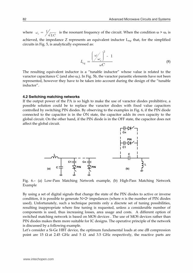
where 1c LCw = is the resonant frequency of the circuit. When the condition ω > ωc is
achieved, the impedance Z represents an equivalent inductor Leq, that, for the simplified circuits in Fig. 5, is analytically expressed as:
2
- 1c
eqL C
www
æ ö÷ç ÷ç ÷çè ø= (8)
The resulting equivalent inductor is a “tunable inductor” whose value is related to the varactor capacitance C (and also ωc). In Fig. 5b, the varactor parasitic elements have not been represented, however they have to be taken into account during the design of the “tunable inductor”.
4.2 Switching matching networks If the output power of the PA is so high to make the use of varactor diodes prohibitive, a possible solution could be to replace the varactor diodes with fixed value capacitors controlled by switching PIN diodes. By observing to the examples in Fig. 6, if the PIN diode connected to the capacitor is in the ON state, the capacitor adds its own capacity to the global circuit. On the other hand, if the PIN diode is in the OFF state, the capacitor does not affect the global circuit.
(b)(a)
L
PIN
Cn
PIN
C1
C
C
L
Cn
PIN
C1
Fig. 6.– (a) Low-Pass Matching Network example, (b) High-Pass Matching Network Example By using a set of digital signals that change the state of the PIN diodes to active or inverse condition, it is possible to generate N=2n impedances (where n is the number of PIN diodes used). Unfortunately, such a technique permits only a discrete set of tuning possibilities, resulting inappropriate where fine tuning is requested, unless a considerable number of components is used, thus increasing losses, area usage and costs. A different option of switched matching network is based on MOS devices . The use of MOS devices rather than PIN diodes makes them more suitable for IC designs. The operative principle of the network is discussed by a following example. Let’s consider a Si-Ge HBT device, the optimum fundamental loads at one dB compression point are 15 at 2.45 GHz and 5 and 3.5 GHz respectively, the reactive parts are
negligible. These resistance values have been determinate accounting for the output power level to be supplied by the power amplifier in the two different bands. The aim of the output network consists in synthesizing these loads using a MOS switching network topology, schematically depicted in Fig. 7 and investigating the general features.
Fig. 7. MOS based switched matching network topology The basic simple network topology is based on a -structure, with an additional branch composed by a NMOS device acting as a switch, with in series an inductor to change the network impedance when the switch is closed. The behavior of the network depends on the switch condition:
1. when the switch is ON (i.e. its Rds value is low, zero in the ideal case) the network should present at its input an impedance value equal to 15 that is the optimum value for the device at 2.45 GHz.
2. When the switch is OFF (i.e. its Rds value is high, infinite in the ideal case) of course, the frequency behavior of the network change. In particular the equivalent value of the inductor between the two shunt capacitors becomes equal to the parallel of L1 and L2 and the input impedance of the network decreases to 5 at 3.5 GHz.
Moving on the actual schematic, for the switch it has been necessary to introduce the biasing network in order to guarantee the right switching functionalities. The simulations have been performed biasing the NMOS device, with dc voltages on drain and source set to VD=3V and VS=3V respectively, to ensure that the NMOS device is properly biased in the origin of its output characteristics. The gate control voltage is raised to VG=5V, when the NMOS switch has to realize a short circuit condition, and dropped to VG=2V when the NMOS switch has to realize an open circuit condition. The feed lines for all three terminals have been realized using 4.8 K resistor for each lines to guarantee the request isolation. Fig. 8 shows the small signal parameters S11 and S21 of the networks, as a function of frequency from 1 GHz to 4 GHz, respectively when the switch is OFF, e.g. when the network has to synthesize the load at 3.5 GHz, and when the switch is ON, e.g. when has to be synthesized the load at 2.45 GHz. In particular in Fig. 8 left, the blue line in the right part of the figure represents the real part of the input impedance, which can be note is roughly equal to 15 ohm. Unfortunately, the input impedance shows a residual imaginary part due to the non ideal behavior of the inductor and capacitor elements present in the network. Similarly, Fig. 8 right reports the same features when the switch is OFF, e.g. when the network has to realize the load
www.intechopen.com

Flexible Power Ampliier Architectures for Spectrum Eficient Wireless Applications 83
where 1c LCw = is the resonant frequency of the circuit. When the condition ω > ωc is
achieved, the impedance Z represents an equivalent inductor Leq, that, for the simplified circuits in Fig. 5, is analytically expressed as:
2
- 1c
eqL C
www
æ ö÷ç ÷ç ÷çè ø= (8)
The resulting equivalent inductor is a “tunable inductor” whose value is related to the varactor capacitance C (and also ωc). In Fig. 5b, the varactor parasitic elements have not been represented, however they have to be taken into account during the design of the “tunable inductor”.
4.2 Switching matching networks If the output power of the PA is so high to make the use of varactor diodes prohibitive, a possible solution could be to replace the varactor diodes with fixed value capacitors controlled by switching PIN diodes. By observing to the examples in Fig. 6, if the PIN diode connected to the capacitor is in the ON state, the capacitor adds its own capacity to the global circuit. On the other hand, if the PIN diode is in the OFF state, the capacitor does not affect the global circuit.
(b)(a)
L
PIN
Cn
PIN
C1
C
C
L
Cn
PIN
C1
Fig. 6.– (a) Low-Pass Matching Network example, (b) High-Pass Matching Network Example By using a set of digital signals that change the state of the PIN diodes to active or inverse condition, it is possible to generate N=2n impedances (where n is the number of PIN diodes used). Unfortunately, such a technique permits only a discrete set of tuning possibilities, resulting inappropriate where fine tuning is requested, unless a considerable number of components is used, thus increasing losses, area usage and costs. A different option of switched matching network is based on MOS devices . The use of MOS devices rather than PIN diodes makes them more suitable for IC designs. The operative principle of the network is discussed by a following example. Let’s consider a Si-Ge HBT device, the optimum fundamental loads at one dB compression point are 15 at 2.45 GHz and 5 and 3.5 GHz respectively, the reactive parts are
negligible. These resistance values have been determinate accounting for the output power level to be supplied by the power amplifier in the two different bands. The aim of the output network consists in synthesizing these loads using a MOS switching network topology, schematically depicted in Fig. 7 and investigating the general features.
Fig. 7. MOS based switched matching network topology The basic simple network topology is based on a -structure, with an additional branch composed by a NMOS device acting as a switch, with in series an inductor to change the network impedance when the switch is closed. The behavior of the network depends on the switch condition:
1. when the switch is ON (i.e. its Rds value is low, zero in the ideal case) the network should present at its input an impedance value equal to 15 that is the optimum value for the device at 2.45 GHz.
2. When the switch is OFF (i.e. its Rds value is high, infinite in the ideal case) of course, the frequency behavior of the network change. In particular the equivalent value of the inductor between the two shunt capacitors becomes equal to the parallel of L1 and L2 and the input impedance of the network decreases to 5 at 3.5 GHz.
Moving on the actual schematic, for the switch it has been necessary to introduce the biasing network in order to guarantee the right switching functionalities. The simulations have been performed biasing the NMOS device, with dc voltages on drain and source set to VD=3V and VS=3V respectively, to ensure that the NMOS device is properly biased in the origin of its output characteristics. The gate control voltage is raised to VG=5V, when the NMOS switch has to realize a short circuit condition, and dropped to VG=2V when the NMOS switch has to realize an open circuit condition. The feed lines for all three terminals have been realized using 4.8 K resistor for each lines to guarantee the request isolation. Fig. 8 shows the small signal parameters S11 and S21 of the networks, as a function of frequency from 1 GHz to 4 GHz, respectively when the switch is OFF, e.g. when the network has to synthesize the load at 3.5 GHz, and when the switch is ON, e.g. when has to be synthesized the load at 2.45 GHz. In particular in Fig. 8 left, the blue line in the right part of the figure represents the real part of the input impedance, which can be note is roughly equal to 15 ohm. Unfortunately, the input impedance shows a residual imaginary part due to the non ideal behavior of the inductor and capacitor elements present in the network. Similarly, Fig. 8 right reports the same features when the switch is OFF, e.g. when the network has to realize the load
www.intechopen.com

Advanced Microwave Circuits and Systems84
required at 3.5GHz. Also in this case, the network exhibits the requested real part of the input impedance, with a residual imaginary part of the input impedance.
Fig. 8. S11 and S21 frequency behavior together with the real and imaginary parts of the input impedance when the switch is ON (left) and OFF (right).
5. Dual-Band reconfigurable SiGe HBT amplifier design
The above described matching network can been adopted to implement the two matching networks for a class-AB amplifier. In the following example of such design approach is presented. The design of the reconfigurable PA is based on a power device composed of 17x8 elementary SiGe HBT with and emitter area of 8.49 m2. The bias circuitry of the power section is designed to provide other than the required base bias current, a circuit-level linearization. Let’s start introducing this latter part, referencing to the Fig. 9. The size of the devices used for the bias circuitry and the values of passive components scale accordingly, so that accurate (i.e. matched) current mirroring can take place. In addition, resistor R4 introduces base ballasting and its value is selected to be 350 Ω per emitter. It helps in reducing the risks due to thermal runaway. A larger value would have better effect, however, that could result in high DC voltage drop at high power drive, and thus early gain compression of T4, the power transistor, would take place.
Fig. 9. PA core schematic including the power transistor and the bias network The power device, which is shown in Fig. 9 within the dotted outline, is biased through the current mirror. By inspection of this figure the current through the reference transistor T1 is:
( )2
1REF be
REFV V
IR
-= , (9)
with Vbe ~ 0.8 V. If the ratio between the reference device and the RF device is M, in this case M = 17x8, then the current that will flow through the RF transistor is M*Iref. in addition, the current mirror behaves like an ideal voltage source, since its output impedance is
1Rout g A
m loop» , (10)
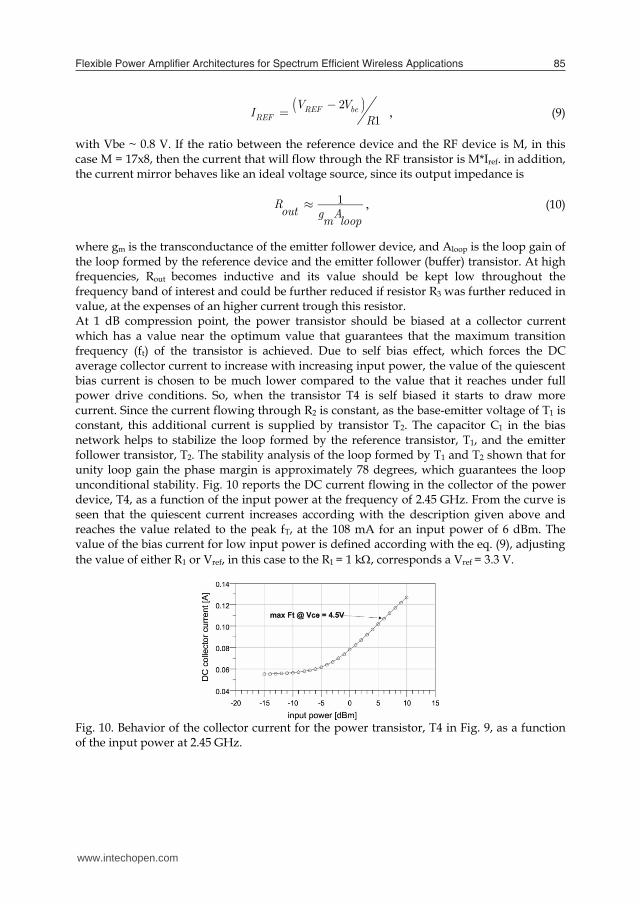
where gm is the transconductance of the emitter follower device, and Aloop is the loop gain of the loop formed by the reference device and the emitter follower (buffer) transistor. At high frequencies, Rout becomes inductive and its value should be kept low throughout the frequency band of interest and could be further reduced if resistor R3 was further reduced in value, at the expenses of an higher current trough this resistor. At 1 dB compression point, the power transistor should be biased at a collector current which has a value near the optimum value that guarantees that the maximum transition frequency (ft) of the transistor is achieved. Due to self bias effect, which forces the DC average collector current to increase with increasing input power, the value of the quiescent bias current is chosen to be much lower compared to the value that it reaches under full power drive conditions. So, when the transistor T4 is self biased it starts to draw more current. Since the current flowing through R2 is constant, as the base-emitter voltage of T1 is constant, this additional current is supplied by transistor T2. The capacitor C1 in the bias network helps to stabilize the loop formed by the reference transistor, T1, and the emitter follower transistor, T2. The stability analysis of the loop formed by T1 and T2 shown that for unity loop gain the phase margin is approximately 78 degrees, which guarantees the loop unconditional stability. Fig. 10 reports the DC current flowing in the collector of the power device, T4, as a function of the input power at the frequency of 2.45 GHz. From the curve is seen that the quiescent current increases according with the description given above and reaches the value related to the peak fT, at the 108 mA for an input power of 6 dBm. The value of the bias current for low input power is defined according with the eq. (9), adjusting the value of either R1 or Vref, in this case to the R1 = 1 k, corresponds a Vref = 3.3 V.
Fig. 10. Behavior of the collector current for the power transistor, T4 in Fig. 9, as a function of the input power at 2.45 GHz.
www.intechopen.com
Flexible Power Ampliier Architectures for Spectrum Eficient Wireless Applications 85
required at 3.5GHz. Also in this case, the network exhibits the requested real part of the input impedance, with a residual imaginary part of the input impedance.
Fig. 8. S11 and S21 frequency behavior together with the real and imaginary parts of the input impedance when the switch is ON (left) and OFF (right).
5. Dual-Band reconfigurable SiGe HBT amplifier design
The above described matching network can been adopted to implement the two matching networks for a class-AB amplifier. In the following example of such design approach is presented. The design of the reconfigurable PA is based on a power device composed of 17x8 elementary SiGe HBT with and emitter area of 8.49 m2. The bias circuitry of the power section is designed to provide other than the required base bias current, a circuit-level linearization. Let’s start introducing this latter part, referencing to the Fig. 9. The size of the devices used for the bias circuitry and the values of passive components scale accordingly, so that accurate (i.e. matched) current mirroring can take place. In addition, resistor R4 introduces base ballasting and its value is selected to be 350 Ω per emitter. It helps in reducing the risks due to thermal runaway. A larger value would have better effect, however, that could result in high DC voltage drop at high power drive, and thus early gain compression of T4, the power transistor, would take place.
Fig. 9. PA core schematic including the power transistor and the bias network The power device, which is shown in Fig. 9 within the dotted outline, is biased through the current mirror. By inspection of this figure the current through the reference transistor T1 is:
( )2
1REF be
REFV V
IR
-= , (9)
with Vbe ~ 0.8 V. If the ratio between the reference device and the RF device is M, in this case M = 17x8, then the current that will flow through the RF transistor is M*Iref. in addition, the current mirror behaves like an ideal voltage source, since its output impedance is
1Rout g A
m loop» , (10)
where gm is the transconductance of the emitter follower device, and Aloop is the loop gain of the loop formed by the reference device and the emitter follower (buffer) transistor. At high frequencies, Rout becomes inductive and its value should be kept low throughout the frequency band of interest and could be further reduced if resistor R3 was further reduced in value, at the expenses of an higher current trough this resistor. At 1 dB compression point, the power transistor should be biased at a collector current which has a value near the optimum value that guarantees that the maximum transition frequency (ft) of the transistor is achieved. Due to self bias effect, which forces the DC average collector current to increase with increasing input power, the value of the quiescent bias current is chosen to be much lower compared to the value that it reaches under full power drive conditions. So, when the transistor T4 is self biased it starts to draw more current. Since the current flowing through R2 is constant, as the base-emitter voltage of T1 is constant, this additional current is supplied by transistor T2. The capacitor C1 in the bias network helps to stabilize the loop formed by the reference transistor, T1, and the emitter follower transistor, T2. The stability analysis of the loop formed by T1 and T2 shown that for unity loop gain the phase margin is approximately 78 degrees, which guarantees the loop unconditional stability. Fig. 10 reports the DC current flowing in the collector of the power device, T4, as a function of the input power at the frequency of 2.45 GHz. From the curve is seen that the quiescent current increases according with the description given above and reaches the value related to the peak fT, at the 108 mA for an input power of 6 dBm. The value of the bias current for low input power is defined according with the eq. (9), adjusting the value of either R1 or Vref, in this case to the R1 = 1 k, corresponds a Vref = 3.3 V.
Fig. 10. Behavior of the collector current for the power transistor, T4 in Fig. 9, as a function of the input power at 2.45 GHz.
www.intechopen.com
Advanced Microwave Circuits and Systems86
The layout of the reconfigurable PA is illustrated in Fig. 11 (left), where are clearly visible the inductors adopted for the matching and the area for the active part of circuit. The total size of the layout with the bonding pads is 1x1mm. While in operation, the voltage in the node between the inductors swings between positive and negative values. This causes the control MOS drain-bulk np junction to be forwarded biased, which degrades switch performance and may results in latchup. In order to overcome the specific drawback, we set an offset voltage (pin Vofs) which shifts the voltage in the abovementioned node in positive values.
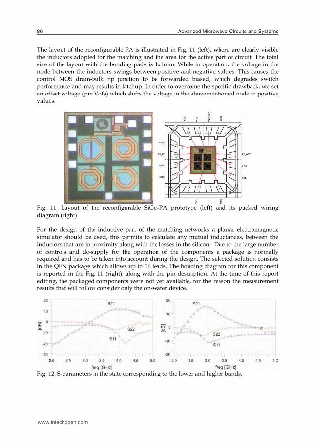
Fig. 11. Layout of the reconfigurable SiGe–PA prototype (left) and its packed wiring diagram (right) For the design of the inductive part of the matching networks a planar electromagnetic simulator should be used, this permits to calculate any mutual inductances, between the inductors that are in proximity along with the losses in the silicon. Due to the large number of controls and dc-supply for the operation of the components a package is normally required and has to be taken into account during the design. The selected solution consists in the QFN package which allows up to 16 leads. The bonding diagram for this component is reported in the Fig. 11 (right), along with the pin description. At the time of this report editing, the packaged components were not yet available, for the reason the measurement results that will follow consider only the on-wafer device.
Fig. 12. S-parameters in the state corresponding to the lower and higher bands.
The first test of measured data considers s-parameter in the range 2 to 5 GHz. The S21-S11 and S22 in dB for the state corresponding to the lower and higher frequency band are reported in Fig. 12. From the figures is clearly observed the shift in frequency due to the above mentioned reasons, which is estimated in the range of 500 MHz. While the small-signal gain maximum is 2.5 dB lower than the simulated in the lower frequency band and 1 dB less in the higher band. This reduced matching have to be attributed to the matching which, being lower than estimated for the discussed reasons, introduces and matching loss consistent with the reduced gain observed during the characterization phase. We exclude problems related to the measurement set and calibration, although a problem related to measurements, the ringing in the 4.7GHz, was observed. The characterization of the sample in the large-signal regime is reported in the below figures. It is carried out at the frequencies where the device exhibits the maximum gain and matching in the two states that are respectively at 2.9GHz and 3.9GHz, which correspond to 500MHz frequency shift from the design target as discussed above. The data related to the large signal gain up to the compression are reported in the Fig. 13, respectively for the state corresponding to the lower and higher frequency. In this figure the CW single tone signal is applied in the two states and the Pout-Pin curves are recorded. The value of the gain is consistent with the small-signal gain while the compression point is estimated to be about 16 dBm for the lower band and 15 dBm for the higher frequency. These figures are 1 dB lower that estimated during the simulations. All this data are consistent with the simulation and again supports the hypothesis that introducing the additional inductive parts due to the packaging the proper frequency behavior can be reached. An intermodulation product characterization considering a two-tone signal with a center frequency at the selected frequencies of 2.9GHz and 3.9GHz and 1MHz offset, was applied to the device. The input power was swept from -10dBm to 13dBm. The results of the characterization, in terms of the higher IM3 are reported in the Fig. 13. It is observed that any consistent change in slope is observed in the traces. This allows concluding that the MOS involved in the switched matching networks doesn’t introduce any additional nonlinearities. In fact, if the additional nonlinearity required changing the state of the device, was effectively excited we would have observed an addition component in the IM3. It is also worth to observe that the input power dealt by the device is below the threshold for which this effects become evident. This threshold from simulation is estimated in the range of 28-30 dBm.
Fig. 13. single tone large-signal gain at 2.9GHz and 3.9GHz and two-tone large-signal inter-modulation offset frequency 1MHz, data reported for the higher IM3 (left), PAE
www.intechopen.com

Flexible Power Ampliier Architectures for Spectrum Eficient Wireless Applications 87
The layout of the reconfigurable PA is illustrated in Fig. 11 (left), where are clearly visible the inductors adopted for the matching and the area for the active part of circuit. The total size of the layout with the bonding pads is 1x1mm. While in operation, the voltage in the node between the inductors swings between positive and negative values. This causes the control MOS drain-bulk np junction to be forwarded biased, which degrades switch performance and may results in latchup. In order to overcome the specific drawback, we set an offset voltage (pin Vofs) which shifts the voltage in the abovementioned node in positive values.
Fig. 11. Layout of the reconfigurable SiGe–PA prototype (left) and its packed wiring diagram (right) For the design of the inductive part of the matching networks a planar electromagnetic simulator should be used, this permits to calculate any mutual inductances, between the inductors that are in proximity along with the losses in the silicon. Due to the large number of controls and dc-supply for the operation of the components a package is normally required and has to be taken into account during the design. The selected solution consists in the QFN package which allows up to 16 leads. The bonding diagram for this component is reported in the Fig. 11 (right), along with the pin description. At the time of this report editing, the packaged components were not yet available, for the reason the measurement results that will follow consider only the on-wafer device.
Fig. 12. S-parameters in the state corresponding to the lower and higher bands.
The first test of measured data considers s-parameter in the range 2 to 5 GHz. The S21-S11 and S22 in dB for the state corresponding to the lower and higher frequency band are reported in Fig. 12. From the figures is clearly observed the shift in frequency due to the above mentioned reasons, which is estimated in the range of 500 MHz. While the small-signal gain maximum is 2.5 dB lower than the simulated in the lower frequency band and 1 dB less in the higher band. This reduced matching have to be attributed to the matching which, being lower than estimated for the discussed reasons, introduces and matching loss consistent with the reduced gain observed during the characterization phase. We exclude problems related to the measurement set and calibration, although a problem related to measurements, the ringing in the 4.7GHz, was observed. The characterization of the sample in the large-signal regime is reported in the below figures. It is carried out at the frequencies where the device exhibits the maximum gain and matching in the two states that are respectively at 2.9GHz and 3.9GHz, which correspond to 500MHz frequency shift from the design target as discussed above. The data related to the large signal gain up to the compression are reported in the Fig. 13, respectively for the state corresponding to the lower and higher frequency. In this figure the CW single tone signal is applied in the two states and the Pout-Pin curves are recorded. The value of the gain is consistent with the small-signal gain while the compression point is estimated to be about 16 dBm for the lower band and 15 dBm for the higher frequency. These figures are 1 dB lower that estimated during the simulations. All this data are consistent with the simulation and again supports the hypothesis that introducing the additional inductive parts due to the packaging the proper frequency behavior can be reached. An intermodulation product characterization considering a two-tone signal with a center frequency at the selected frequencies of 2.9GHz and 3.9GHz and 1MHz offset, was applied to the device. The input power was swept from -10dBm to 13dBm. The results of the characterization, in terms of the higher IM3 are reported in the Fig. 13. It is observed that any consistent change in slope is observed in the traces. This allows concluding that the MOS involved in the switched matching networks doesn’t introduce any additional nonlinearities. In fact, if the additional nonlinearity required changing the state of the device, was effectively excited we would have observed an addition component in the IM3. It is also worth to observe that the input power dealt by the device is below the threshold for which this effects become evident. This threshold from simulation is estimated in the range of 28-30 dBm.
Fig. 13. single tone large-signal gain at 2.9GHz and 3.9GHz and two-tone large-signal inter-modulation offset frequency 1MHz, data reported for the higher IM3 (left), PAE
www.intechopen.com

Advanced Microwave Circuits and Systems88
6. Dual-band power amplifier architectures
The main objective of this paragraph is about the consistent and quantitative evaluation of a two possible architectures of dual-band PA both suitable for their involvement in the concurrent dual-band systems, [12]. The first is based on two dedicated PAs combined by a frequency diplexer while the second is specifically designed to be operated in dual-band state. For the sake of the comparison the operative frequency are defined as 1.98 and 3.42 GHz respectively suitable for WCDMA and OFDM radio access technologies. The two dual-band architectures considered in this paragraph are based on the schematic representations reported in Fig. 14. In the first (Fig. 14, left) the PA is implemented by making use of two dedicated PAs combined by a frequency diplexer. This latter device has to be designed to combine the two PAs introducing band-pass and band-stop behavior in each of the two branches. This is implement by the most innovative technique and technology and it still represents a very critical part of the entire PA structure. Indeed, this component must guarantee an almost lossless behavior in the two transmission paths and as much as possible isolation between them; without sacrificing the matching. In particular the transmission loss characteristic is required to preserve the combined efficiency of the entire structure, while the isolation is a required feature to avoid the cross-modulation between the two dedicated PAs. The constraints on the diplexer become more critical in the case of closer operative spectrum bands. During the two dedicated PAs design, the eventual combination with the diplexer implies a specific additional PA design consideration related to an accurate evaluation of the out-of band termination, which might degrade the output power and efficiency of the two units. The treatment of the harmonic termination of the due to the diplexer is out of the scope for the present treatment.
Fig. 14. Schematic of the concurrent dual-band PA implemented by two combined dedicated PAs (left), and by a dual-band PA (right). Either the dedicated frequency PAs and concurrent PA topology consist of conventional class-AB PA designs, where the tuned matching networks can be synthesized by either passive and\or distributed elements properly dimensioned, without external tuning controls. For the concurrent PA (Fig. 14, right), the two signal sources are combined prior to
be applied to the PA input. The design method of concurrent dual-band PA based on multi-tuned networks composed of lumped elements is discussed in [10]. The investigation carried out in this chapter relies on prototypes designed and fabricated using low cost off the shelf active devices along with discrete SMD passive components assembled on FR4 0.8 mm thick evaluation printed circuit board designed with microstrip technology. For this specific test several electron device technology can be considered, eider bipolar or FET fabricated using several different material, spanning from Si to GaAs and possibly GaN. In the present case we choose as active device a GaAs FET, namely the ATF50189 from AVAGO Technologies, a medium power enhanced mode p-HEMT with a cut off frequency of 6 GHz and a 1-dB compression point of 29 dBm at 2 GHz. Optimum bias point for efficiency, linearity and gain can be fund either from manufacturer specifications or CAD simulations, on the basis of nonlinear model analysis. For the specific device possible bias point is found to be 4.5V drain supply voltage with a corresponding quiescent current of 200 mA. The chosen bias point drives the ATF50189 transistor in the AB class operation. The design was based on load and source pull simulations carried out at the two fundamental frequencies of 1.98 and 3.42 GHz, adopting a nonlinear device model which included the package parasitic. Simulations provided saturated output power of 28 dBm and 26 dBm respectively in the lower and higher frequency bands with a power added efficiency of approximately 40% and 35% at the 1-dB gain compression point. The resulting load and source constant power contours are shown respectively in Fig. 15.
Fig. 15. Simulated source-pull (left) load-pull (right)contours at 1.98 GHz and 3.42GHz, 1 dB steps, and terminations at fundamentals for the single band and dual-band prototypes The implementation of the source and load terminations defined by the source- and load-pull analysis was obtained by using lumped elements matching networks. This technique, by employing a different approach with respect to standard microstrip technology, enabled the achievement of highly compact prototypes. All the designed PAs adopt the same general topology for the input and output matching networks. Different nominal values and the absence of some of the components determine the difference between the prototypes. In addition, the input network accommodates a stabilizing network which has bee implemented by all three prototypes. The presence of shunt capacitors at both the gate and drain terminals, provide a short circuit to the second harmonic.
www.intechopen.com

Flexible Power Ampliier Architectures for Spectrum Eficient Wireless Applications 89
6. Dual-band power amplifier architectures
The main objective of this paragraph is about the consistent and quantitative evaluation of a two possible architectures of dual-band PA both suitable for their involvement in the concurrent dual-band systems, [12]. The first is based on two dedicated PAs combined by a frequency diplexer while the second is specifically designed to be operated in dual-band state. For the sake of the comparison the operative frequency are defined as 1.98 and 3.42 GHz respectively suitable for WCDMA and OFDM radio access technologies. The two dual-band architectures considered in this paragraph are based on the schematic representations reported in Fig. 14. In the first (Fig. 14, left) the PA is implemented by making use of two dedicated PAs combined by a frequency diplexer. This latter device has to be designed to combine the two PAs introducing band-pass and band-stop behavior in each of the two branches. This is implement by the most innovative technique and technology and it still represents a very critical part of the entire PA structure. Indeed, this component must guarantee an almost lossless behavior in the two transmission paths and as much as possible isolation between them; without sacrificing the matching. In particular the transmission loss characteristic is required to preserve the combined efficiency of the entire structure, while the isolation is a required feature to avoid the cross-modulation between the two dedicated PAs. The constraints on the diplexer become more critical in the case of closer operative spectrum bands. During the two dedicated PAs design, the eventual combination with the diplexer implies a specific additional PA design consideration related to an accurate evaluation of the out-of band termination, which might degrade the output power and efficiency of the two units. The treatment of the harmonic termination of the due to the diplexer is out of the scope for the present treatment.
Fig. 14. Schematic of the concurrent dual-band PA implemented by two combined dedicated PAs (left), and by a dual-band PA (right). Either the dedicated frequency PAs and concurrent PA topology consist of conventional class-AB PA designs, where the tuned matching networks can be synthesized by either passive and\or distributed elements properly dimensioned, without external tuning controls. For the concurrent PA (Fig. 14, right), the two signal sources are combined prior to
be applied to the PA input. The design method of concurrent dual-band PA based on multi-tuned networks composed of lumped elements is discussed in [10]. The investigation carried out in this chapter relies on prototypes designed and fabricated using low cost off the shelf active devices along with discrete SMD passive components assembled on FR4 0.8 mm thick evaluation printed circuit board designed with microstrip technology. For this specific test several electron device technology can be considered, eider bipolar or FET fabricated using several different material, spanning from Si to GaAs and possibly GaN. In the present case we choose as active device a GaAs FET, namely the ATF50189 from AVAGO Technologies, a medium power enhanced mode p-HEMT with a cut off frequency of 6 GHz and a 1-dB compression point of 29 dBm at 2 GHz. Optimum bias point for efficiency, linearity and gain can be fund either from manufacturer specifications or CAD simulations, on the basis of nonlinear model analysis. For the specific device possible bias point is found to be 4.5V drain supply voltage with a corresponding quiescent current of 200 mA. The chosen bias point drives the ATF50189 transistor in the AB class operation. The design was based on load and source pull simulations carried out at the two fundamental frequencies of 1.98 and 3.42 GHz, adopting a nonlinear device model which included the package parasitic. Simulations provided saturated output power of 28 dBm and 26 dBm respectively in the lower and higher frequency bands with a power added efficiency of approximately 40% and 35% at the 1-dB gain compression point. The resulting load and source constant power contours are shown respectively in Fig. 15.
Fig. 15. Simulated source-pull (left) load-pull (right)contours at 1.98 GHz and 3.42GHz, 1 dB steps, and terminations at fundamentals for the single band and dual-band prototypes The implementation of the source and load terminations defined by the source- and load-pull analysis was obtained by using lumped elements matching networks. This technique, by employing a different approach with respect to standard microstrip technology, enabled the achievement of highly compact prototypes. All the designed PAs adopt the same general topology for the input and output matching networks. Different nominal values and the absence of some of the components determine the difference between the prototypes. In addition, the input network accommodates a stabilizing network which has bee implemented by all three prototypes. The presence of shunt capacitors at both the gate and drain terminals, provide a short circuit to the second harmonic.
www.intechopen.com

Advanced Microwave Circuits and Systems90
Fig. 16. Prototypes input (left) and output (right) matching network circuit schematic The selected matching networks pi-topology, exhibits high out of band frequency roll off and a null in the transfer characteristic between the two fundamental frequency bands at 1.98 GHz and 3.42 GHz so enhancing isolation between frequency bands. In order to properly define the networks the additional conditions for maximum efficiency and 1-dB compression output power under large signal excitations were taken into account. To simplify the description we can consider that the three prototypes adopt the same general topology for the input and output matching networks, whose schematics are represented in Fig. 16. As far as the networks dimensioning is of concern, it is possible to show that the 4 unknown (2 inductors and 2 capacitors for each network) are calculated solving a nonlinear system of four equations, where the number of equations results directly equating the two real parts and the two imaginary parts of the equivalent impedance, in symbolic format, with the required optimum impedances. Different nominal values and the absence of some of the components will determine the difference between the prototypes. In addition to matching purpose the input network accommodates a stabilizing network which is common for all the three prototypes. The resulting matching networks result very compact and capable to satisfy the conditions for the optimization of both the output power and gain. The presence of shunt capacitors at both the gate and drain terminals, C2 and C4 in the figures, provide a short circuits at the second harmonics. The resulting best values for the SMD capacitances and inductances are those indicated in Table 1 and Table 1. Input matching network L-C values respectively for the input and output matching networks. The achieved impedance are reported in the Fig. 16 where the mismatch between the actual values and the optimum impedances for power level take into account for the additional condition of gain and commercial availability of the nominal values.
C1 L1 C2 L2
concurrent dual band 1.7 nH 0.33 pF 7.6 nH 0.3 pF
single band at 1.98GHz 0.6 nH 1.47 pF n.a. n.a.
single band 3.42GHz 1.6 nH 0.26 pF n.a. n.a.
Table 1. Input matching network L-C values
C4 L4 C3 L3
concurrent dual band 0.6 pF 3.2 nH 0.77 pF 2.88 nH
single band at 1.98GHz n.a. n.a. 1.7 nH 1.9 pF
single band 3.42GHz n.a. n.a. 1.1 nH 0.5 pF
Table 2. Output matching network L-C values The three PA modules were fabricated using FR4 PCB technology and then adopted to implement the two dual-band PA configurations, namely the combined PAs and the dual-band PA. The diplexer used in the large-signal test benches it is realized in microstrip technology and provides an insertion loss of 0.6 dB and 0.8 dB respectively at 1.9 GHz and 3.4 GHz, and isolation between the two channels better than 30 dB and a return loss higher than 20 dB.
Fig. 17. Measured small-signal gain for the concurrent dual-band and the two single band prototypes The preliminary test was performed in small signal regime to assess the prototypes performance and to verify the consistency of the comparison. The measured small signal gains associated with the concurrent dual-band PA and with the two single-band PAs prototypes are compared in Fig. 17. The figure indicates that at 1.98 GHz the maximum linear gain is approximately 11dB for both single band and dual band circuits. In the 3.4 GHz band the PA prototypes exhibit a maximum linear gain of 6 dB at 3.42 GHz, and present a 0.5dB gain bandwidth of approximately 60 MHz. Input and output return losses are not reported but are below –15 dB in the respective frequency bands for all the PAs. Small signal characterizations have indicated a very close correspondence between the single band circuits and the concurrent dual band PA in terms of both input/output return loss and gain. This results show that the design of a concurrent dual-band PA using compact lumped elements is feasible without loss of performance at small-signal and makes the characterization and comparison with large and modulated signals meaningful. The first set of large signal measurements test bench is deployed to fully characterise the PA prototypes with CW large signal excitations. The data are useful to compare the maximum linear power, the gain and the efficiency of the two architectures. In particular the comparison between the power gains as a function of the two CW signals at 1.98 GHz (namely F1) and 3.4 GHz (namely F2), reported in Fig. 18, shows that the combined PA
www.intechopen.com

Flexible Power Ampliier Architectures for Spectrum Eficient Wireless Applications 91
Fig. 16. Prototypes input (left) and output (right) matching network circuit schematic The selected matching networks pi-topology, exhibits high out of band frequency roll off and a null in the transfer characteristic between the two fundamental frequency bands at 1.98 GHz and 3.42 GHz so enhancing isolation between frequency bands. In order to properly define the networks the additional conditions for maximum efficiency and 1-dB compression output power under large signal excitations were taken into account. To simplify the description we can consider that the three prototypes adopt the same general topology for the input and output matching networks, whose schematics are represented in Fig. 16. As far as the networks dimensioning is of concern, it is possible to show that the 4 unknown (2 inductors and 2 capacitors for each network) are calculated solving a nonlinear system of four equations, where the number of equations results directly equating the two real parts and the two imaginary parts of the equivalent impedance, in symbolic format, with the required optimum impedances. Different nominal values and the absence of some of the components will determine the difference between the prototypes. In addition to matching purpose the input network accommodates a stabilizing network which is common for all the three prototypes. The resulting matching networks result very compact and capable to satisfy the conditions for the optimization of both the output power and gain. The presence of shunt capacitors at both the gate and drain terminals, C2 and C4 in the figures, provide a short circuits at the second harmonics. The resulting best values for the SMD capacitances and inductances are those indicated in Table 1 and Table 1. Input matching network L-C values respectively for the input and output matching networks. The achieved impedance are reported in the Fig. 16 where the mismatch between the actual values and the optimum impedances for power level take into account for the additional condition of gain and commercial availability of the nominal values.
C1 L1 C2 L2
concurrent dual band 1.7 nH 0.33 pF 7.6 nH 0.3 pF
single band at 1.98GHz 0.6 nH 1.47 pF n.a. n.a.
single band 3.42GHz 1.6 nH 0.26 pF n.a. n.a.
Table 1. Input matching network L-C values
C4 L4 C3 L3
concurrent dual band 0.6 pF 3.2 nH 0.77 pF 2.88 nH
single band at 1.98GHz n.a. n.a. 1.7 nH 1.9 pF
single band 3.42GHz n.a. n.a. 1.1 nH 0.5 pF
Table 2. Output matching network L-C values The three PA modules were fabricated using FR4 PCB technology and then adopted to implement the two dual-band PA configurations, namely the combined PAs and the dual-band PA. The diplexer used in the large-signal test benches it is realized in microstrip technology and provides an insertion loss of 0.6 dB and 0.8 dB respectively at 1.9 GHz and 3.4 GHz, and isolation between the two channels better than 30 dB and a return loss higher than 20 dB.
Fig. 17. Measured small-signal gain for the concurrent dual-band and the two single band prototypes The preliminary test was performed in small signal regime to assess the prototypes performance and to verify the consistency of the comparison. The measured small signal gains associated with the concurrent dual-band PA and with the two single-band PAs prototypes are compared in Fig. 17. The figure indicates that at 1.98 GHz the maximum linear gain is approximately 11dB for both single band and dual band circuits. In the 3.4 GHz band the PA prototypes exhibit a maximum linear gain of 6 dB at 3.42 GHz, and present a 0.5dB gain bandwidth of approximately 60 MHz. Input and output return losses are not reported but are below –15 dB in the respective frequency bands for all the PAs. Small signal characterizations have indicated a very close correspondence between the single band circuits and the concurrent dual band PA in terms of both input/output return loss and gain. This results show that the design of a concurrent dual-band PA using compact lumped elements is feasible without loss of performance at small-signal and makes the characterization and comparison with large and modulated signals meaningful. The first set of large signal measurements test bench is deployed to fully characterise the PA prototypes with CW large signal excitations. The data are useful to compare the maximum linear power, the gain and the efficiency of the two architectures. In particular the comparison between the power gains as a function of the two CW signals at 1.98 GHz (namely F1) and 3.4 GHz (namely F2), reported in Fig. 18, shows that the combined PA
www.intechopen.com

Advanced Microwave Circuits and Systems92
architecture is capable to maintain the two channels mostly separated producing a gain compression which is insensible from the concurrent signal at the side band. In fact the contour plots show a linear behaviour which is independent of the power level in the other channel. At the contrary for the dual-band PA, the mutual interaction between signals at the two frequencies is evidenced by bended constant gain loci, see Fig. 19. Nevertheless, although the effect of the side band is quite evident, the effect of the output diplexer is such that the maximum output power was slightly higher. For example, we can notice that at 1.98 GHz for input power equal to 16 dBm the gain is 8.7 dB for the combined PAs while 9.5 dB for the dual band. This latter condition is maintained only when the input signal at 3.4 GHz is lower than 10 dBm. Similar behaviour is observed in respect to the power gain calculated at 3.4 GHz. From the contour plots it is observed that the loci corresponding to 8.5 dB and 4 dB correspond to the linear gain that the dual-band PA can provide and, consequently, the input ranges which guarantee the linear operation of the PA. Differently, in the case of the combined PAs, the linearity in one frequency band does not depend of the side band.
Fig. 18. Power gain [dB] in large signal regime evaluated at the frequency of 1.98 GHz (left) 3.4 GHz (right) as function of input power at 1.98 GHz (F1) and 3.45 GHz (F2), for the combined PAs architecture.
Fig. 19. Power gain [dB] in large signal regime evaluated at the frequency of 1.98 GHz (left) 3.4 GHz (right) and as function of input power at 1.98 GHz (F1) and 3.45 GHz (F2), for the dual-band PA architecture.
From the contour plots it is observed in the case of the combined PAs and in the case of the dual band PA, the presence of the diplexer and the mutual interaction between carriers respectively, determine the output power in correspondence of a 1-dB compressed power gain reported in Table 3. This latter consideration leads to the conclusion that from the point of view of the CW output power there are not differences between the two architectures. This latter consideration leads to the conclusion that from the maximum output power in CW condition there are not differences between the two possible architectures.
architecture 1.98 GHz 3.4 GHz
Combined PAs 25 dBm 22 dBm Dual-band PA 24.5 dBm 23 dBm
Table 3. Simultaneous maximum linear output power (at 1 dB gain compression) A further very significant figure is represented by the Power Added Efficiency (PAE) for the two PA architectures. In the case of dual-band concurrent PA the PAE is calculated by:
( ) ( )1 1 2 2F F F Fload av load av
dc
P P P PPAE
P
- + -= , (11)
The above equation admits that the two signal are uncorrelated and where Pdc takes into account for the total current drawn by the PA modules. The PAE as a function of the input power at the two carrier frequencies, respectively for the combined PAs and the dual band PA architectures are reported in Fig. 20.
Fig. 20. Power added efficiency [%] in large signal regime as function of input power at 1.98 GHz (F1) and 3.45 GHz (F2), for the combined PAs architecture, (left), and the dual-band PA architecture, (right). From these experimental verification it is confirmed the intuition that the dual-band PA PAE takes advantage from the current reuse which is inherent in the use of a single power device, when compared with the case of the combined PAs which need twice of the DC power to bias the two PAs. This determine an almost factor 2 in the PAE for the dual-band PA for almost the entire range of evaluation. In particular at 1-dB gain compression the PAE achieved with the combined PAs architecture is in the range of 20%, as evidenced in Fig. 20 left, while in the case of the dual-band PA it reaches 32 %, see Fig. 20 right. The maxima are 28 % and 44% respectively for the combined PAs and the dual band PA architectures. By this figure we can observe a significant improvement of the dual-band PA with respect to
www.intechopen.com

Flexible Power Ampliier Architectures for Spectrum Eficient Wireless Applications 93
architecture is capable to maintain the two channels mostly separated producing a gain compression which is insensible from the concurrent signal at the side band. In fact the contour plots show a linear behaviour which is independent of the power level in the other channel. At the contrary for the dual-band PA, the mutual interaction between signals at the two frequencies is evidenced by bended constant gain loci, see Fig. 19. Nevertheless, although the effect of the side band is quite evident, the effect of the output diplexer is such that the maximum output power was slightly higher. For example, we can notice that at 1.98 GHz for input power equal to 16 dBm the gain is 8.7 dB for the combined PAs while 9.5 dB for the dual band. This latter condition is maintained only when the input signal at 3.4 GHz is lower than 10 dBm. Similar behaviour is observed in respect to the power gain calculated at 3.4 GHz. From the contour plots it is observed that the loci corresponding to 8.5 dB and 4 dB correspond to the linear gain that the dual-band PA can provide and, consequently, the input ranges which guarantee the linear operation of the PA. Differently, in the case of the combined PAs, the linearity in one frequency band does not depend of the side band.
Fig. 18. Power gain [dB] in large signal regime evaluated at the frequency of 1.98 GHz (left) 3.4 GHz (right) as function of input power at 1.98 GHz (F1) and 3.45 GHz (F2), for the combined PAs architecture.
Fig. 19. Power gain [dB] in large signal regime evaluated at the frequency of 1.98 GHz (left) 3.4 GHz (right) and as function of input power at 1.98 GHz (F1) and 3.45 GHz (F2), for the dual-band PA architecture.
From the contour plots it is observed in the case of the combined PAs and in the case of the dual band PA, the presence of the diplexer and the mutual interaction between carriers respectively, determine the output power in correspondence of a 1-dB compressed power gain reported in Table 3. This latter consideration leads to the conclusion that from the point of view of the CW output power there are not differences between the two architectures. This latter consideration leads to the conclusion that from the maximum output power in CW condition there are not differences between the two possible architectures.
architecture 1.98 GHz 3.4 GHz
Combined PAs 25 dBm 22 dBm Dual-band PA 24.5 dBm 23 dBm
Table 3. Simultaneous maximum linear output power (at 1 dB gain compression) A further very significant figure is represented by the Power Added Efficiency (PAE) for the two PA architectures. In the case of dual-band concurrent PA the PAE is calculated by:
( ) ( )1 1 2 2F F F Fload av load av
dc
P P P PPAE
P
- + -= , (11)
The above equation admits that the two signal are uncorrelated and where Pdc takes into account for the total current drawn by the PA modules. The PAE as a function of the input power at the two carrier frequencies, respectively for the combined PAs and the dual band PA architectures are reported in Fig. 20.
Fig. 20. Power added efficiency [%] in large signal regime as function of input power at 1.98 GHz (F1) and 3.45 GHz (F2), for the combined PAs architecture, (left), and the dual-band PA architecture, (right). From these experimental verification it is confirmed the intuition that the dual-band PA PAE takes advantage from the current reuse which is inherent in the use of a single power device, when compared with the case of the combined PAs which need twice of the DC power to bias the two PAs. This determine an almost factor 2 in the PAE for the dual-band PA for almost the entire range of evaluation. In particular at 1-dB gain compression the PAE achieved with the combined PAs architecture is in the range of 20%, as evidenced in Fig. 20 left, while in the case of the dual-band PA it reaches 32 %, see Fig. 20 right. The maxima are 28 % and 44% respectively for the combined PAs and the dual band PA architectures. By this figure we can observe a significant improvement of the dual-band PA with respect to
www.intechopen.com

Advanced Microwave Circuits and Systems94
the combined PAs architecture. The absolute maximum power for the two PAs are reported in the Fig. 21, calculated by summing the power level at the two carrier frequencies, assumed uncorrelated. Form the contour plots is observed that, regardless linearity concerns, the total power provided by the two systems are slightly the same.
Fig. 21. Total output power [dBm] in large signal regime as function of input power at 1.98 GHz (F1) and 3.45 GHz (F2), for the combined PAs architecture (left) and for the dual-band PA architecture, (right). The next test concerns about the capability of the dual-band PA architecture to deal with modulated signals and its performance are compared with the combined single band PAs; henceforth the combined PAs architecture is not longer considered. In this case, the base-band signals were down-loaded in the arbitrary signal generators (Agilent ESG 4438C) by using the tools available in the Agilent ADS2006A systems. Two different digitally modulated signals were employed to evaluate PA performance: a 3GPP up-link W-CDMA 3.84 MHz chip rate signal at 1.98 GHz and a 5MHz OFDM 16-QAM signal at 3.42GHz corresponding to one of the WiMAX modes. The output of the PA under test was connected to the VSA (Agilent N9020, 26MHz bandwidth) which was synchronized with the two arbitrary signal generators. The first set of data refers to the large signal gain plotted against the output power for the three PA modules; the comparisons between several operating conditions are shown in Fig. 22, left and right, for the lower and higher frequency bands respectively, which include also CW for the sake of a better comparison.
Fig. 22. Gain curve versus output power for CW and WCDMA modulated excitations, both with carrier at 1.98 GHz (left) and 3.42 GHz (right).
It is observed that when the amplifiers are driven by a single modulated signal peak power at 1dB gain compression point decreases: this effect is explained by the fact that gain compression in PAs driven by digitally modulated signals occurs at lower power levels than for 1-tone CW signals. In addition, load pull CAD analysis and successive design were performed based on a CW test signal, while experimental results show that the optimum load impedance for maximum linear output power as well as peak efficiency varies depending on the characteristics of the input signal, i.e. pulsed, modulated or CW. Concurrent mode was then operated by simultaneously feeding the dual-band PA with OFDM and WCDMA signals at the two center band frequencies. Reduction of peak output power with respect to single-channel excitations is mainly due to the simultaneous presence of two modulated signals in the same device which cause cross-modulation between the two time varying envelopes. A resulting 4 dB and a 4.5 dB peak power reduction at 1.98 GHz and at 3.42 GHz respectively were measured with respect to the single channel cases. Moving on to system level figures, the 5.6% EVM WiMax standard limit and a minimum ACPR of 33dBc for a WCDMA signal as settled by the 3GPP specifications have been taken as a reference for power and efficiency values. The goal of the large signal characterisation has so being focussed on the evaluation of the peak output powers and the resulting PAE levels achievable in the two frequency bands with both concurrent dual-band and single-band excitations so as to satisfy EVM and ACPR constrains.
Fig. 23. (Left) Adjacent channel power ratio measured at 5 MHz offset and integrated over the bandwidth, for the single band and the dual-band prototypes with the WCDMA signal at 1.98 GHz; (Right) Error vector magnitude measured for the single band and the dual-band prototypes with the OFDM signal at 3.42 GHz. From Fig. 23 it is observed that at 1.98 GHz the maximum achievable output power, due to ACPR constrains, is 27.5 dBm when the dual-band PA is working in single-channel mode, while for the concurrent dual-band case this limit decreases to 23 dBm. Data in Fig. 23 show EVM versus the output power results, for single channel operation and dual band mode at 3.42 GHz: a maximum output power of 20 dBm is achieved in the first case while when the dual-band PA is working in concurrent mode, maximum output power settles to 17 dBm. The above data indicate that a significant change in performance arises when the PA is driven in the concurrent dual band mode, specifically resulting in a peak power back off of about 4.5 dB and 3dB respectively for the lower and higher frequency bands due to meet the
www.intechopen.com

Flexible Power Ampliier Architectures for Spectrum Eficient Wireless Applications 95
the combined PAs architecture. The absolute maximum power for the two PAs are reported in the Fig. 21, calculated by summing the power level at the two carrier frequencies, assumed uncorrelated. Form the contour plots is observed that, regardless linearity concerns, the total power provided by the two systems are slightly the same.
Fig. 21. Total output power [dBm] in large signal regime as function of input power at 1.98 GHz (F1) and 3.45 GHz (F2), for the combined PAs architecture (left) and for the dual-band PA architecture, (right). The next test concerns about the capability of the dual-band PA architecture to deal with modulated signals and its performance are compared with the combined single band PAs; henceforth the combined PAs architecture is not longer considered. In this case, the base-band signals were down-loaded in the arbitrary signal generators (Agilent ESG 4438C) by using the tools available in the Agilent ADS2006A systems. Two different digitally modulated signals were employed to evaluate PA performance: a 3GPP up-link W-CDMA 3.84 MHz chip rate signal at 1.98 GHz and a 5MHz OFDM 16-QAM signal at 3.42GHz corresponding to one of the WiMAX modes. The output of the PA under test was connected to the VSA (Agilent N9020, 26MHz bandwidth) which was synchronized with the two arbitrary signal generators. The first set of data refers to the large signal gain plotted against the output power for the three PA modules; the comparisons between several operating conditions are shown in Fig. 22, left and right, for the lower and higher frequency bands respectively, which include also CW for the sake of a better comparison.
Fig. 22. Gain curve versus output power for CW and WCDMA modulated excitations, both with carrier at 1.98 GHz (left) and 3.42 GHz (right).
It is observed that when the amplifiers are driven by a single modulated signal peak power at 1dB gain compression point decreases: this effect is explained by the fact that gain compression in PAs driven by digitally modulated signals occurs at lower power levels than for 1-tone CW signals. In addition, load pull CAD analysis and successive design were performed based on a CW test signal, while experimental results show that the optimum load impedance for maximum linear output power as well as peak efficiency varies depending on the characteristics of the input signal, i.e. pulsed, modulated or CW. Concurrent mode was then operated by simultaneously feeding the dual-band PA with OFDM and WCDMA signals at the two center band frequencies. Reduction of peak output power with respect to single-channel excitations is mainly due to the simultaneous presence of two modulated signals in the same device which cause cross-modulation between the two time varying envelopes. A resulting 4 dB and a 4.5 dB peak power reduction at 1.98 GHz and at 3.42 GHz respectively were measured with respect to the single channel cases. Moving on to system level figures, the 5.6% EVM WiMax standard limit and a minimum ACPR of 33dBc for a WCDMA signal as settled by the 3GPP specifications have been taken as a reference for power and efficiency values. The goal of the large signal characterisation has so being focussed on the evaluation of the peak output powers and the resulting PAE levels achievable in the two frequency bands with both concurrent dual-band and single-band excitations so as to satisfy EVM and ACPR constrains.
Fig. 23. (Left) Adjacent channel power ratio measured at 5 MHz offset and integrated over the bandwidth, for the single band and the dual-band prototypes with the WCDMA signal at 1.98 GHz; (Right) Error vector magnitude measured for the single band and the dual-band prototypes with the OFDM signal at 3.42 GHz. From Fig. 23 it is observed that at 1.98 GHz the maximum achievable output power, due to ACPR constrains, is 27.5 dBm when the dual-band PA is working in single-channel mode, while for the concurrent dual-band case this limit decreases to 23 dBm. Data in Fig. 23 show EVM versus the output power results, for single channel operation and dual band mode at 3.42 GHz: a maximum output power of 20 dBm is achieved in the first case while when the dual-band PA is working in concurrent mode, maximum output power settles to 17 dBm. The above data indicate that a significant change in performance arises when the PA is driven in the concurrent dual band mode, specifically resulting in a peak power back off of about 4.5 dB and 3dB respectively for the lower and higher frequency bands due to meet the
www.intechopen.com

Advanced Microwave Circuits and Systems96
EVM and ACPR restrictions. Envelope cross-modulation and inter-modulation explain the EVM and ACPR increased growth with input power when compared with single channel mode. Experimental data showed that a 2 dB back-off is necessary with concurrent operation to maintain the EVM at 4.1%. It can be concluded that the proposed solution is capable to provide the same system level performance of more conventional solutions while increasing the overall PAE and allowing a significant reduction of the system complexity. A further implementation of dual band PA in GaN technology can be found in [13].
7. Dual-band power amplifier digital linearization
As discussed in the above paragraphs, the application of digitally modulated signals to a PA, which is considered hereinafter as an nonlinear (NL) dynamic system, causes in-band distortion and spectrum spreading and finally determine a degradation of the signal quality. The most effective broadband linearization systems have usually been based upon the feedforward technique [14]. However, RF and baseband predistortion linearization techniques have become an attractive solution owing to their reduced cost and complexity. For multicarrier PA applications, an effort has been placed to increase the bandwidth of predistortion linearization to combat fast memory effects. Baseband Digital Predistortion (DP) seems to be the most promising one. It works by the introduction, in the digital baseband, of an opposite NL of the PA’s one, allowing for greater efficiency through a significant power backoff reduction. The most of the available DP techniques deal with single-band operation, although recently an approach to deal with multi-carrier and potentially for multiband systems was presented in [15]. In this technique the modulation bandwidth in several bands and then a DP algorithm is applied selectively the inband and interband third-order intermodulation distortion (IMD3) As the approach relies on third order Volterra model the accuracy of the DP depends upon the identification procedure and the frequency band spacing. Here we discuss a novel method of Dual Band DP (DB-DP), based on the simultaneous predistortion of both channels at intermediate frequency (IF), [16]. The proposed method uses a single band memory polynomial DP for linearization. As a feedback path we propose a subsampling receiver.
7.1 Basic principles of digital linearization Let’s start reviewing the basic concepts of the DP system. It consists basically in the introduction, at the baseband, of a subsystems which has a transfer function which is opposite to the one of the PA, as in Fig. 24.
Fig. 24. Predistorsion Principle applied to a nonlinear system The predistorter can be Look-Up Table (LUT) based or polynomial-based: in the first case, a LUT indexed by the input power is filled with complex coefficients, and the input ( )x n is multiplied with the corrisponding one; in the second, the complex coefficients of a k-order
polynomial approximating the inverse of the PA’s characteristics are found, and the DP output ( )z n is given by:
1 2 3( ) ( ) ( ) ( )z n a x n a x n a x n= + + + (12) The coefficients vector a can be found through a recursive algorithm based on the Indirect Learning architecture shown in Fig. 25. The name derives from the fact that the polynomial coefficients are found without passing by the determination of the PA’s characteristics.
Fig. 25. Indirect Learning schematic principle for a DPD system The indirect learning techniques works by two identical predistorters, the first – the actual one – in the transmission path and the second – the training one – in the feedback path. The outputs of both are compared to produce an error signal: ˆ( ) ( ) ( )e n z n z n= - (13)
where ( )z n is the output of the training DP. It can be demonstrated that when the error energy is zero the PA’s baseband output ( )y t is linear with the baseband input ( )x n , that is the cascade of predistorter and amplifier becomes linear. If the PA’s memory length is comparable to the envelope variations of the signal, the baseband model – which we call memory polynomial – can be adopted:
1
1, o d
1,
0d
( ) ( ) ( )K L
kk
kk
ll
y n z n l z nb l
(14)
where K represent the order of the DP, while L is the number of memory samples; the baseband equivalent input ( )z n , the output ( )y n and the coefficients ,k lb of the model, are all complex valued in general. The predistorter’s output can be written the same way:
1
1, o d
1,
0d
( ) x( ) ( )K
kk
Lk
k ll
z n n l x na l
(15)
It has to be equal to the Training DP’s output ( )z n to minimize the error energy, that is:
1
11
,,
odd0
y( ) y( )( ) kK L
k llk
k
n l n lz nK K
a
(16)
The objective consists in finding the parameters ,k la that define the predistorter. Since ( )z n is
linear in the ,k la , the latter can be estimated by a simple least-squares method. By defining a new sequence:
www.intechopen.com

Flexible Power Ampliier Architectures for Spectrum Eficient Wireless Applications 97
EVM and ACPR restrictions. Envelope cross-modulation and inter-modulation explain the EVM and ACPR increased growth with input power when compared with single channel mode. Experimental data showed that a 2 dB back-off is necessary with concurrent operation to maintain the EVM at 4.1%. It can be concluded that the proposed solution is capable to provide the same system level performance of more conventional solutions while increasing the overall PAE and allowing a significant reduction of the system complexity. A further implementation of dual band PA in GaN technology can be found in [13].
7. Dual-band power amplifier digital linearization
As discussed in the above paragraphs, the application of digitally modulated signals to a PA, which is considered hereinafter as an nonlinear (NL) dynamic system, causes in-band distortion and spectrum spreading and finally determine a degradation of the signal quality. The most effective broadband linearization systems have usually been based upon the feedforward technique [14]. However, RF and baseband predistortion linearization techniques have become an attractive solution owing to their reduced cost and complexity. For multicarrier PA applications, an effort has been placed to increase the bandwidth of predistortion linearization to combat fast memory effects. Baseband Digital Predistortion (DP) seems to be the most promising one. It works by the introduction, in the digital baseband, of an opposite NL of the PA’s one, allowing for greater efficiency through a significant power backoff reduction. The most of the available DP techniques deal with single-band operation, although recently an approach to deal with multi-carrier and potentially for multiband systems was presented in [15]. In this technique the modulation bandwidth in several bands and then a DP algorithm is applied selectively the inband and interband third-order intermodulation distortion (IMD3) As the approach relies on third order Volterra model the accuracy of the DP depends upon the identification procedure and the frequency band spacing. Here we discuss a novel method of Dual Band DP (DB-DP), based on the simultaneous predistortion of both channels at intermediate frequency (IF), [16]. The proposed method uses a single band memory polynomial DP for linearization. As a feedback path we propose a subsampling receiver.
7.1 Basic principles of digital linearization Let’s start reviewing the basic concepts of the DP system. It consists basically in the introduction, at the baseband, of a subsystems which has a transfer function which is opposite to the one of the PA, as in Fig. 24.
Fig. 24. Predistorsion Principle applied to a nonlinear system The predistorter can be Look-Up Table (LUT) based or polynomial-based: in the first case, a LUT indexed by the input power is filled with complex coefficients, and the input ( )x n is multiplied with the corrisponding one; in the second, the complex coefficients of a k-order
polynomial approximating the inverse of the PA’s characteristics are found, and the DP output ( )z n is given by:
1 2 3( ) ( ) ( ) ( )z n a x n a x n a x n= + + + (12) The coefficients vector a can be found through a recursive algorithm based on the Indirect Learning architecture shown in Fig. 25. The name derives from the fact that the polynomial coefficients are found without passing by the determination of the PA’s characteristics.
Fig. 25. Indirect Learning schematic principle for a DPD system The indirect learning techniques works by two identical predistorters, the first – the actual one – in the transmission path and the second – the training one – in the feedback path. The outputs of both are compared to produce an error signal: ˆ( ) ( ) ( )e n z n z n= - (13)
where ( )z n is the output of the training DP. It can be demonstrated that when the error energy is zero the PA’s baseband output ( )y t is linear with the baseband input ( )x n , that is the cascade of predistorter and amplifier becomes linear. If the PA’s memory length is comparable to the envelope variations of the signal, the baseband model – which we call memory polynomial – can be adopted:
1
1, o d
1,
0d
( ) ( ) ( )K L
kk
kk
ll
y n z n l z nb l
(14)
where K represent the order of the DP, while L is the number of memory samples; the baseband equivalent input ( )z n , the output ( )y n and the coefficients ,k lb of the model, are all complex valued in general. The predistorter’s output can be written the same way:
1
1, o d
1,
0d
( ) x( ) ( )K
kk
Lk
k ll
z n n l x na l
(15)
It has to be equal to the Training DP’s output ( )z n to minimize the error energy, that is:
1
11
,,
odd0
y( ) y( )( ) kK L
k llk
k
n l n lz nK K
a
(16)
The objective consists in finding the parameters ,k la that define the predistorter. Since ( )z n is
linear in the ,k la , the latter can be estimated by a simple least-squares method. By defining a new sequence:
www.intechopen.com

Advanced Microwave Circuits and Systems98
1
,y( ) y( )( )
k
k ln l n lu nK K
(17)
we can rewrite ( )z n in matrix form as: z Ua (18) where ,[ (0 ( )), ]1 Tz nz -=z , 0[ , , ]L=U U U , 1[ , , ]l l Kl= uU u , [ (0), ( 1, )]Tkl kl klu u N= -u and
10 10[ , ,, , , ], TK KQQa a a a=a . The least-squares solution for a is given by:
1[ ]H Ha U U U z (19)
where (·)H denotes complex conjugate transpose. A direct implementation of the polynomial predistorter is difficult, because it requires several sample-per-sample multiplications and power raisings. However, an efficient implementation is possible by observing that (15) is equivalent to:
1, 1, odd odd
1 1
1, od
,0 ,1
1, 1
d
( ) ( ) x( ) ( 1) x( 1)
( 1) x( 1)
k kk k
K Kk k
k k
Kk
k Lkk
z n a x n n a x n n
a x n L n L
(20)
The nonlinear polynomial can be implemented with a LUT indexed by the input magnitude, ( )x n l [1]. This way, only L complex multiplications per sample are needed. LUT
coefficients calculation is performed once the ,k la are found. The performance of the
memory polynomial-LUT predistorter depends on the number of quantization points, on the memory length L and on the order of the polynomial,K .
7.2 Sub-sampling receiver A key component for the DB-DP is the sub-sampling receiver, it operates on the principle of the band-pass sampling theorem, and it is used as feedback path of the DP system. If RF signals have a narrow bandwidth B, they can be sampled with a frequency: 2
sf B³ (21)
As a result of the sampling process, spectrum aliases are generated around all the multiples of sf as in Fig. 26. The image that falls in [0; / 2]
sf (first Nyquist zone) is the exact
representation of the input signal, unless a potential phase inversion, and can be digitized. The same principle can also be used to convert two (or more) band-pass signals
1s and
2s ,
located at different carrier frequencies 1cf and
2cf , with band-widths B1 and B2 . With a
proper sampling frequency there will be replicas of the two signals located side-by-side in the first Nyquist zone with no overlap, as shown in Fig. 27. The proper sampling frequency respect the condition:
1 22( )
sBf B³ + (22)
That is, a Nyquist Zone must be wider than the sum of the two bands.
Fig. 26. Single band band-pass sub-sampling principle
Fig. 27. Dual band sub-sampling principle The condition of no overlap consists of the both signals to be comprised in a single half-Nyquist zone, i.e. [ ;( 1) // 44 ]
s snf n f+ , where n is integer. If we define:
1 1
2
2 2
1
/ 2 / 2c cf B f BK floor Q floor
B B
æ ö æ ö- -÷ ÷ç ç÷ ÷= =ç ç÷ ÷ç ç÷ ÷ç çè ø è ø (23)
where ()floor is the operation of rounding to the lower integer, the conditions of no overlap are first given by:
1
2
1 1
2 2
/ 4 / 2 1) / 4 / 2(
(/ 4 / 2 1) / 4 / 2s c s
s c s
kf B k f B
qf B f B
k
f
f q
K
q Q
£ ££
ìï + + -ïïï + + -ïïíïï£î
££
ïïïï
(24)
where k and q are integers identifying the order of the half-Zone in which the first and the second signals stand, respectively. The other condition, i.e. standing in central vs. peripheral half-zones, are given by:
www.intechopen.com

Flexible Power Ampliier Architectures for Spectrum Eficient Wireless Applications 99
1
,y( ) y( )( )
k
k ln l n lu nK K
(17)
we can rewrite ( )z n in matrix form as: z Ua (18) where ,[ (0 ( )), ]1 Tz nz -=z , 0[ , , ]L=U U U , 1[ , , ]l l Kl= uU u , [ (0), ( 1, )]Tkl kl klu u N= -u and
10 10[ , ,, , , ], TK KQQa a a a=a . The least-squares solution for a is given by:
1[ ]H Ha U U U z (19)
where (·)H denotes complex conjugate transpose. A direct implementation of the polynomial predistorter is difficult, because it requires several sample-per-sample multiplications and power raisings. However, an efficient implementation is possible by observing that (15) is equivalent to:
1, 1, odd odd
1 1
1, od
,0 ,1
1, 1
d
( ) ( ) x( ) ( 1) x( 1)
( 1) x( 1)
k kk k
K Kk k
k k
Kk
k Lkk
z n a x n n a x n n
a x n L n L
(20)
The nonlinear polynomial can be implemented with a LUT indexed by the input magnitude, ( )x n l [1]. This way, only L complex multiplications per sample are needed. LUT
coefficients calculation is performed once the ,k la are found. The performance of the
memory polynomial-LUT predistorter depends on the number of quantization points, on the memory length L and on the order of the polynomial,K .
7.2 Sub-sampling receiver A key component for the DB-DP is the sub-sampling receiver, it operates on the principle of the band-pass sampling theorem, and it is used as feedback path of the DP system. If RF signals have a narrow bandwidth B, they can be sampled with a frequency: 2
sf B³ (21)
As a result of the sampling process, spectrum aliases are generated around all the multiples of sf as in Fig. 26. The image that falls in [0; / 2]
sf (first Nyquist zone) is the exact
representation of the input signal, unless a potential phase inversion, and can be digitized. The same principle can also be used to convert two (or more) band-pass signals
1s and
2s ,
located at different carrier frequencies 1cf and
2cf , with band-widths B1 and B2 . With a
proper sampling frequency there will be replicas of the two signals located side-by-side in the first Nyquist zone with no overlap, as shown in Fig. 27. The proper sampling frequency respect the condition:
1 22( )
sBf B³ + (22)
That is, a Nyquist Zone must be wider than the sum of the two bands.
Fig. 26. Single band band-pass sub-sampling principle
Fig. 27. Dual band sub-sampling principle The condition of no overlap consists of the both signals to be comprised in a single half-Nyquist zone, i.e. [ ;( 1) // 44 ]
s snf n f+ , where n is integer. If we define:
1 1
2
2 2
1
/ 2 / 2c cf B f BK floor Q floor
B B
æ ö æ ö- -÷ ÷ç ç÷ ÷= =ç ç÷ ÷ç ç÷ ÷ç çè ø è ø (23)
where ()floor is the operation of rounding to the lower integer, the conditions of no overlap are first given by:
1
2
1 1
2 2
/ 4 / 2 1) / 4 / 2(
(/ 4 / 2 1) / 4 / 2s c s
s c s
kf B k f B
qf B f B
k
f
f q
K
q Q
£ ££
ìï + + -ïïï + + -ïïíïï£î
££
ïïïï
(24)
where k and q are integers identifying the order of the half-Zone in which the first and the second signals stand, respectively. The other condition, i.e. standing in central vs. peripheral half-zones, are given by:
www.intechopen.com

Advanced Microwave Circuits and Systems100
4 ,4 1
4 ,4 1
4 2,4 1
4 2,4
4
4 1
4 1
4 2 1
n n
n n
n
K n Q
K n Q
K n Q
K n Q
n
n n
¹ -¹ -¹
ìï = ïïï = - ïïíï = + ïïï = + ïïî
+ +¹ + +
(25)
These conditions lead to a not closed form formulation which require an iterative approach for the solution. Once the suitable sampling frequency is found, the two signals replicas in the first Nyquist zone are located at the frequencies
1bbf and
2bbf which are given by:
( )
( )
1
11
2
22
( / 4)· 4 , 4 1
( / 4) 1 · 4 2, 4 1
( / 4)· 4 , 4 1
( / 4) 1 · 4 2, 4 1
c s
bbs c
c s
bbs c
f floor k f k n k nf
floor k f f k n k n
f floor q f q n q nf
floor q f f q n q n
ìï - = = +ïï= íï + - = + = -ïïîìï - = = +ïï= íï + - = + = -ïïî
(26)
The distortion introduced by a sub-sampling receiver is due in large part to the transfer function of the sampling device. In general, a T/H is preferred over a S/H, because of the lower distortion and higher sampling frequency reachable. The transfer function of a T/H is:
( )( )( )
( ) sinc sincs
s
nj T
Tj f sss
s s s sn
T n TnG f G f f e e
T T T T
p tpt t tt
t+¥ -
-
=-¥
ùæ ö é æ ö- - ú÷ ÷ç çê÷ ÷= - + úç ç÷ ÷ç çê÷ ÷ç ç úè ø è øë úûå , (27)
where sT is the sampling period and t is the length of the hold period. Due to the sinc() in order to avoid an amplitude distortion, t should be as low as possible to move at high frequency the first null. Also, the baseband aliases should be as near as possible to the zero. As regards the phase, different replicas have a different offset depending on the order n and the frequency of the alias. Replicas falling into the first Nyquist zone have a phase offset depending on k and
1BBf , or q and
2BBf . This offset must be compensated if a synchronism
between the two signals is necessary, as in our proposed Dual Band DP method. This approach exhibits some critical points, [17]. The first ones to be considered are noise aliasing and aperture jitter; then out-of-bands signals and wideband noise must be filtered out before the sampler. That noise would otherwise, after sampling, translate and accumulate into the rst Nyquist zone. Besides, as even a perfect filter would reject the noise introduced by downstream circuits, low noise components have to be chosen. However, noise aliasing reduces with sampling frequency increase. Aperture jitter can be treated as a white noise if the jitter is low, and it doesn’t depend on the sampling frequency. When designing a sub-sampling receiver, another important parameter to take care of is the analog bandwidth of the sampler, that must be greater than the highest frequency of the RF signals.
7.3 Dual Band Digital Predistortion Architecture The DP-DP is achieved by a RF-level predistortion: a signal predistorter (as opposed to a data predistorter) is able to treat any kind of signal, that is it doesn’t depend either on the
bandwidth or the center frequency. Let’s consider an input signal made of the superposition of two signals at different center frequencies, that is 21( ) ( ) ( )n x n x nx = + . The input is predistorted ( ( )z n ), converted into analog ( ( )z t ) and amplified ( ( )y t ). A portion of ( )y t is drawn to have a feedback signal and to train the DP. A scheme is shown in Fig. 28. The main problem with this setup is the lack of sufficiently fast D/A and A/D converters, that will remain so in the foreseeable future because ADC dynamic range and conversion are known to progress at a rate much slower than Moore’s law. Also, a RF predistortion is not possible at the moment, because it must be performed sample-per-sample and the sample rate is at least twice the maximum RF frequency (baseband sampling theorem).
Fig. 28. RF DB-DP, principle of operation
Actually, the converters related problem can be easily overcome. The RF DAC can be replaced by two baseband DAC preceded by a proper digital filtering and digital frequency conversion system. In a similar way, the RF ADC can be replaced by two frequency converters and two baseband ADCs. There remains the sample rate problem. The last limit can be overcome by introducing a new architecture which is capable to lowering the sample rate, that is predistorting at intermediate frequency (IF). In this case the baseband digital signals
1( )x n and
2( )x n are
shifted to 1IFf and
2IFf then summed, creating ( )'x n . This IF signal is predistorted ( ( )'z n ),
and the two bands are separated and shifted to the baseband to be analog converted. The analog PA’s input ( )'z t is built by those baseband signals, shifted to the RF frequencies
1cf
and 2cf . It is amplified ( ( )'y t ) and a portion of it is drawn to create the feedback signals. As
a feedback path we propose a subsampling receiver: the two bands composing ( )'y t are aliased side-by-side in the baseband, then digitized by a single ADC. In the digital domain, the bands are separated and shifted to IF, composing the signal ' ( )'y n that will be compared to ( )'x n .
www.intechopen.com

Flexible Power Ampliier Architectures for Spectrum Eficient Wireless Applications 101
4 ,4 1
4 ,4 1
4 2,4 1
4 2,4
4
4 1
4 1
4 2 1
n n
n n
n
K n Q
K n Q
K n Q
K n Q
n
n n
¹ -¹ -¹
ìï = ïïï = - ïïíï = + ïïï = + ïïî
+ +¹ + +
(25)
These conditions lead to a not closed form formulation which require an iterative approach for the solution. Once the suitable sampling frequency is found, the two signals replicas in the first Nyquist zone are located at the frequencies
1bbf and
2bbf which are given by:
( )
( )
1
11
2
22
( / 4)· 4 , 4 1
( / 4) 1 · 4 2, 4 1
( / 4)· 4 , 4 1
( / 4) 1 · 4 2, 4 1
c s
bbs c
c s
bbs c
f floor k f k n k nf
floor k f f k n k n
f floor q f q n q nf
floor q f f q n q n
ìï - = = +ïï= íï + - = + = -ïïîìï - = = +ïï= íï + - = + = -ïïî
(26)
The distortion introduced by a sub-sampling receiver is due in large part to the transfer function of the sampling device. In general, a T/H is preferred over a S/H, because of the lower distortion and higher sampling frequency reachable. The transfer function of a T/H is:
( )( )( )
( ) sinc sincs
s
nj T
Tj f sss
s s s sn
T n TnG f G f f e e
T T T T
p tpt t tt
t+¥ -
-
=-¥
ùæ ö é æ ö- - ú÷ ÷ç çê÷ ÷= - + úç ç÷ ÷ç çê÷ ÷ç ç úè ø è øë úûå , (27)
where sT is the sampling period and t is the length of the hold period. Due to the sinc() in order to avoid an amplitude distortion, t should be as low as possible to move at high frequency the first null. Also, the baseband aliases should be as near as possible to the zero. As regards the phase, different replicas have a different offset depending on the order n and the frequency of the alias. Replicas falling into the first Nyquist zone have a phase offset depending on k and
1BBf , or q and
2BBf . This offset must be compensated if a synchronism
between the two signals is necessary, as in our proposed Dual Band DP method. This approach exhibits some critical points, [17]. The first ones to be considered are noise aliasing and aperture jitter; then out-of-bands signals and wideband noise must be filtered out before the sampler. That noise would otherwise, after sampling, translate and accumulate into the rst Nyquist zone. Besides, as even a perfect filter would reject the noise introduced by downstream circuits, low noise components have to be chosen. However, noise aliasing reduces with sampling frequency increase. Aperture jitter can be treated as a white noise if the jitter is low, and it doesn’t depend on the sampling frequency. When designing a sub-sampling receiver, another important parameter to take care of is the analog bandwidth of the sampler, that must be greater than the highest frequency of the RF signals.
7.3 Dual Band Digital Predistortion Architecture The DP-DP is achieved by a RF-level predistortion: a signal predistorter (as opposed to a data predistorter) is able to treat any kind of signal, that is it doesn’t depend either on the
bandwidth or the center frequency. Let’s consider an input signal made of the superposition of two signals at different center frequencies, that is 21( ) ( ) ( )n x n x nx = + . The input is predistorted ( ( )z n ), converted into analog ( ( )z t ) and amplified ( ( )y t ). A portion of ( )y t is drawn to have a feedback signal and to train the DP. A scheme is shown in Fig. 28. The main problem with this setup is the lack of sufficiently fast D/A and A/D converters, that will remain so in the foreseeable future because ADC dynamic range and conversion are known to progress at a rate much slower than Moore’s law. Also, a RF predistortion is not possible at the moment, because it must be performed sample-per-sample and the sample rate is at least twice the maximum RF frequency (baseband sampling theorem).
Fig. 28. RF DB-DP, principle of operation
Actually, the converters related problem can be easily overcome. The RF DAC can be replaced by two baseband DAC preceded by a proper digital filtering and digital frequency conversion system. In a similar way, the RF ADC can be replaced by two frequency converters and two baseband ADCs. There remains the sample rate problem. The last limit can be overcome by introducing a new architecture which is capable to lowering the sample rate, that is predistorting at intermediate frequency (IF). In this case the baseband digital signals
1( )x n and
2( )x n are
shifted to 1IFf and
2IFf then summed, creating ( )'x n . This IF signal is predistorted ( ( )'z n ),
and the two bands are separated and shifted to the baseband to be analog converted. The analog PA’s input ( )'z t is built by those baseband signals, shifted to the RF frequencies
1cf
and 2cf . It is amplified ( ( )'y t ) and a portion of it is drawn to create the feedback signals. As
a feedback path we propose a subsampling receiver: the two bands composing ( )'y t are aliased side-by-side in the baseband, then digitized by a single ADC. In the digital domain, the bands are separated and shifted to IF, composing the signal ' ( )'y n that will be compared to ( )'x n .
www.intechopen.com

Advanced Microwave Circuits and Systems102
Fig. 29. DB-DP system with IF predistortion and subsampling feedback The block diagram of the whole system is shown in When using a subsampling receiver, it is necessary to compensate the different phase offset applied to both bands. This may be done in the digital domain. If a T/H is used, the right phase shift can be calculated through eq. (27). Anti-aliasing filters must be carefully designed with in general out of band rejection. The IFs setting is a crucial point of the system design. They have to be far enough to leave room for out-of-band distortion and to simplify filtering; on the other side, they should be as low as possible to reduce computational constraints. As a rule, for the proposed DB-DP you may consider a sample rate at least four times higher than in a SB-DP system. The DB-DP was simulated by Matlab/Simulink®. We considered two 16 QAM signals, with amplitudes 10dBmP = - and centre frequencies 1 2.1cf = GHz and 2 3.5cf = GHz; the sampling frequency was set to 146.5sf = MHz. The PA was modeled with the Wiener-Hammerstein model. LTI blocks preceeding and following the memoryless NL were set to have the following transfer functions:
2 2
1 1,
1 0.5 1 0.3( ) ( )
1 0.4 1 0.4
z zH z z
z zG
- -
- -
+ -= =
- - (28)
It was chosen a tanh-shaped AM/AM NL, that has G=20dB, IP3=38dB and whose AM/PM is linear, with 5°/dB slope.
Fig. 30. Spectra comparison for lower and higher channels, between transmitted signal and input signal, with DB-DP OFF and DB-DP ON (left.
Fig. 31. Constellations comparison for lower (left) and higher (higher) channel, between transmitted signal and input signal, with DB-DP OFF and DB-DP ON For the implementation of the DB-DPD we used a memory polynomial DP, with a memory length of 4 taps, a polynomial order K=9 and a LUT predistorter with a size of 512. Polynomial coefficients were estimated on a basis of 8192 samples. Simulation results for both channels are shown in Fig. 30 and Fig. 31, where an ACPR and EVM significant reduction is observed. The method proved to be able to correct most NLs, but it is not as
www.intechopen.com

Flexible Power Ampliier Architectures for Spectrum Eficient Wireless Applications 103
Fig. 29. DB-DP system with IF predistortion and subsampling feedback The block diagram of the whole system is shown in When using a subsampling receiver, it is necessary to compensate the different phase offset applied to both bands. This may be done in the digital domain. If a T/H is used, the right phase shift can be calculated through eq. (27). Anti-aliasing filters must be carefully designed with in general out of band rejection. The IFs setting is a crucial point of the system design. They have to be far enough to leave room for out-of-band distortion and to simplify filtering; on the other side, they should be as low as possible to reduce computational constraints. As a rule, for the proposed DB-DP you may consider a sample rate at least four times higher than in a SB-DP system. The DB-DP was simulated by Matlab/Simulink®. We considered two 16 QAM signals, with amplitudes 10dBmP = - and centre frequencies 1 2.1cf = GHz and 2 3.5cf = GHz; the sampling frequency was set to 146.5sf = MHz. The PA was modeled with the Wiener-Hammerstein model. LTI blocks preceeding and following the memoryless NL were set to have the following transfer functions:
2 2
1 1,
1 0.5 1 0.3( ) ( )
1 0.4 1 0.4
z zH z z
z zG
- -
- -
+ -= =
- - (28)
It was chosen a tanh-shaped AM/AM NL, that has G=20dB, IP3=38dB and whose AM/PM is linear, with 5°/dB slope.
Fig. 30. Spectra comparison for lower and higher channels, between transmitted signal and input signal, with DB-DP OFF and DB-DP ON (left.
Fig. 31. Constellations comparison for lower (left) and higher (higher) channel, between transmitted signal and input signal, with DB-DP OFF and DB-DP ON For the implementation of the DB-DPD we used a memory polynomial DP, with a memory length of 4 taps, a polynomial order K=9 and a LUT predistorter with a size of 512. Polynomial coefficients were estimated on a basis of 8192 samples. Simulation results for both channels are shown in Fig. 30 and Fig. 31, where an ACPR and EVM significant reduction is observed. The method proved to be able to correct most NLs, but it is not as
www.intechopen.com

Advanced Microwave Circuits and Systems104
good as a SB-DP. While in that case we obtained a Normalized Mean Square Error (NMSE) of 3e-4, in the DB-DP case we obtained an NMSE of 1e-3.
8. Concluding Remarks
The design of flexible PAs and multiband transmitter architectures is at a crucial stage; the number of research teams and projects that approached this field increased over the recent years. The number of special sessions and workshops in the main international conferences confirmed this interest. Some commercial products appeared recently, although they remain mainly based on very simple arrangements of frequency dedicated PAs with limited tuning control. Some technological and methodological problem have to be solved. The first set are related to the device technologies for both the RF power devices and the control devices. Indeed, the energy efficiency and peak power have to be maintained for wideband operation, making the device technology more challenging. Design approach have to take into account for multiband driving which reduce sensibly the power handling capability of the power device. Control devices, like switches and tuning elements have to cope with high peak power increasing the demand of linearity and efficiency, in this field MEMS appears a promising technology. An additional consideration is due for the architectures of multiband-multiband transmitters. Other than flexibility they have to provide excellent signal quality, which is much more threated by simultaneous concurrent signals. Polar transmitters versus Cartesian architectures are investigated as the two mainstreams for future transmitter architectures.
9. Acknowledgement
The contents of this chapter are mainly based on the results of the research activities performed in the context of the project TARGET– “Top Amplifier Research Groups in a European Team” supported by the Information Society Technologies Programme of the EU under contract IST-1-507893-NOE, www.target-net.org.
10. References
[1] Hashimoto, A.; Yoshino, H.; Atarashi, H., "Roadmap of IMT-advanced development," Microwave Magazine, IEEE , vol.9, no.4, pp.80-88, Aug. 2008
[2] F. K. Jondral, "Software-Defined Radio Basics and Evolution to Cognitive Radio", Journal on Wireless Communications and Networking, 2005, vol. 3, 275-283
[3] A. A. Abidi, "The Path to the Software-Defined Radio Receiver", IEEE Journal of Solid-State Circuits, Vol. 42, no. 5, May 2007, pp. 954-966
[4] P. B. Kennington, RF and Baseband Techniques for Software Defined. Radio. Norwell, MA: Artech House, 2005.
[5] J. Laskar, R. Mukhopadhyay, Y. Hur, C. -H. Lee, and K. Lim, "Reconfigurable RFICs and modules for cognitive radio", Digest of Topical Meeting on Silicon Monolithic Integrated Circuits in RF Systems, 2006. Jan. 2006 pp. 18-20
[6] F. Wang, D. F. Kimball, J. D. Popp, A. H. Yang, D. Y. Lie, P. M. Asbeck, L. E. Larson, "An Improved Power-Added Efficiency 19-dBm Hybrid Envelope Elimination and Restoration Power Amplifier for 802.11g WLAN Applications," Trans. On Microwave Theory and Techniques, Vol. 54, Dec. 2006, pp. 4086-4099
[7] Q. Shen, N. S. Barker "Distributed MEMS tunable matching network using minimal-contact RF-MEMS varactors," Microwave Theory and Techniques, IEEE Transactions on , vol.54, no.6, pp.2646-2658, June 2006
[8]K. Buisman, L.C.N. de Vreede, L.E. Larson, M. Spirito, A. Akhnoukh, T.L.M. Scholtes, L.K. Nanver “Distortion-free varactor diode topologies for RF adaptivity”, Microwave Symposium Digest, 2005 IEEE MTT-S International,12-17 June 2005 pp. 157-160
[9]A. Jrad, A.-L. Perrier, R. Bourtoutian, J.-M. Duchamp, P. Ferrari, “Design of an ultra compact electronically tunable microwave impedance transformer”, Electronics Letters, Volume 41, Issue 12, 9 June 2005 pp. 707 – 709
[10]P. Colantonio, F. Giannini, R. Giofrè, L. Piazzon, "Simultaneous Dual-Band High Efficiency Harmonic Tuned Power Amplifier in GaN Technology", European Microwave Conference Digest, Munich Oct., 2007
[11] W.C.E. Neo, Yu Lin, Xiao-dong Liu, L.C.N. de Vreede, L.E. Larson, M. Spirito, M.J. Pelk, K. Buisman, A. Akhnoukh, A. de Graauw, L.K. Nanver, "Adaptive Multi-Band Multi-Mode Power Amplifier Using Integrated Varactor-Based Tunable Matching Networks," Solid-State Circuits, IEEE Journal of , vol.41, no.9, pp.2166-2176, Sept. 2006
[12] A. Cidronali, I. Magrini, N. Giovannelli, M. Mercanti, G. Manes “Experimental system level analysis of a concurrent dual-band power amplifier for WiMAX and WCDMA applications”; International Journal of Microwave and Wireless Technologies, Cambridge University Press and the European Microwave Association, Vol.1 Special Issue 02, April 2009 pp 99-107
[13]P. Colantonio, F. Giannini, R. Giofre, L. Piazzon, “Simultaneous dual-band high efficiency harmonic tuned power amplifier in GaN technology”, European Microwave Integrated Circuit Conference, 8-10 Oct. 2007 pp.127 - 130
[14]R. Meyer, R. Eschenback, and W. Edgerley, Jr., “A wideband feedforward amplifier,” IEEE J. Solid-State Circuits, vol. SCC-9, no. 6, pp. 422–448, Jun. 1974.
[15]P. Roblin, S. K. Myoung, D. Chaillot, Y. Gi Kim, A. Fathimulla, J. Strahler, S. Bibyk”Frequency-Selective Predistortion Linearization of RF Power Amplifiers” IEEE Trans on Microwave Theory and Tech., Vol. 56, Jan. 2008, pp 65-76
[16]A. Cidronali, I. Magrini, R. Fagotti, G. Manes, "A new approach for concurrent Dual-Band IF Digital PreDistortion: System design and analysis," Workshop on Integrated Nonlinear Microwave and Millimetre-Wave Circuits, 2008. INMMIC 2008, pp.127-130, 24-25 Nov. 2008
[17]G. Avitabile, A. Cidronali, G. Manes, ‘A S-band digital down converter for radar applications based on GaAs MMIC fast sample&hold’, IEE Proceedings-Circuits, Device and Systems, Vol.143, No.6 Dec. 1996 pp.337-342
www.intechopen.com

Flexible Power Ampliier Architectures for Spectrum Eficient Wireless Applications 105
good as a SB-DP. While in that case we obtained a Normalized Mean Square Error (NMSE) of 3e-4, in the DB-DP case we obtained an NMSE of 1e-3.
8. Concluding Remarks
The design of flexible PAs and multiband transmitter architectures is at a crucial stage; the number of research teams and projects that approached this field increased over the recent years. The number of special sessions and workshops in the main international conferences confirmed this interest. Some commercial products appeared recently, although they remain mainly based on very simple arrangements of frequency dedicated PAs with limited tuning control. Some technological and methodological problem have to be solved. The first set are related to the device technologies for both the RF power devices and the control devices. Indeed, the energy efficiency and peak power have to be maintained for wideband operation, making the device technology more challenging. Design approach have to take into account for multiband driving which reduce sensibly the power handling capability of the power device. Control devices, like switches and tuning elements have to cope with high peak power increasing the demand of linearity and efficiency, in this field MEMS appears a promising technology. An additional consideration is due for the architectures of multiband-multiband transmitters. Other than flexibility they have to provide excellent signal quality, which is much more threated by simultaneous concurrent signals. Polar transmitters versus Cartesian architectures are investigated as the two mainstreams for future transmitter architectures.
9. Acknowledgement
The contents of this chapter are mainly based on the results of the research activities performed in the context of the project TARGET– “Top Amplifier Research Groups in a European Team” supported by the Information Society Technologies Programme of the EU under contract IST-1-507893-NOE, www.target-net.org.
10. References
[1] Hashimoto, A.; Yoshino, H.; Atarashi, H., "Roadmap of IMT-advanced development," Microwave Magazine, IEEE , vol.9, no.4, pp.80-88, Aug. 2008
[2] F. K. Jondral, "Software-Defined Radio Basics and Evolution to Cognitive Radio", Journal on Wireless Communications and Networking, 2005, vol. 3, 275-283
[3] A. A. Abidi, "The Path to the Software-Defined Radio Receiver", IEEE Journal of Solid-State Circuits, Vol. 42, no. 5, May 2007, pp. 954-966
[4] P. B. Kennington, RF and Baseband Techniques for Software Defined. Radio. Norwell, MA: Artech House, 2005.
[5] J. Laskar, R. Mukhopadhyay, Y. Hur, C. -H. Lee, and K. Lim, "Reconfigurable RFICs and modules for cognitive radio", Digest of Topical Meeting on Silicon Monolithic Integrated Circuits in RF Systems, 2006. Jan. 2006 pp. 18-20
[6] F. Wang, D. F. Kimball, J. D. Popp, A. H. Yang, D. Y. Lie, P. M. Asbeck, L. E. Larson, "An Improved Power-Added Efficiency 19-dBm Hybrid Envelope Elimination and Restoration Power Amplifier for 802.11g WLAN Applications," Trans. On Microwave Theory and Techniques, Vol. 54, Dec. 2006, pp. 4086-4099
[7] Q. Shen, N. S. Barker "Distributed MEMS tunable matching network using minimal-contact RF-MEMS varactors," Microwave Theory and Techniques, IEEE Transactions on , vol.54, no.6, pp.2646-2658, June 2006
[8]K. Buisman, L.C.N. de Vreede, L.E. Larson, M. Spirito, A. Akhnoukh, T.L.M. Scholtes, L.K. Nanver “Distortion-free varactor diode topologies for RF adaptivity”, Microwave Symposium Digest, 2005 IEEE MTT-S International,12-17 June 2005 pp. 157-160
[9]A. Jrad, A.-L. Perrier, R. Bourtoutian, J.-M. Duchamp, P. Ferrari, “Design of an ultra compact electronically tunable microwave impedance transformer”, Electronics Letters, Volume 41, Issue 12, 9 June 2005 pp. 707 – 709
[10]P. Colantonio, F. Giannini, R. Giofrè, L. Piazzon, "Simultaneous Dual-Band High Efficiency Harmonic Tuned Power Amplifier in GaN Technology", European Microwave Conference Digest, Munich Oct., 2007
[11] W.C.E. Neo, Yu Lin, Xiao-dong Liu, L.C.N. de Vreede, L.E. Larson, M. Spirito, M.J. Pelk, K. Buisman, A. Akhnoukh, A. de Graauw, L.K. Nanver, "Adaptive Multi-Band Multi-Mode Power Amplifier Using Integrated Varactor-Based Tunable Matching Networks," Solid-State Circuits, IEEE Journal of , vol.41, no.9, pp.2166-2176, Sept. 2006
[12] A. Cidronali, I. Magrini, N. Giovannelli, M. Mercanti, G. Manes “Experimental system level analysis of a concurrent dual-band power amplifier for WiMAX and WCDMA applications”; International Journal of Microwave and Wireless Technologies, Cambridge University Press and the European Microwave Association, Vol.1 Special Issue 02, April 2009 pp 99-107
[13]P. Colantonio, F. Giannini, R. Giofre, L. Piazzon, “Simultaneous dual-band high efficiency harmonic tuned power amplifier in GaN technology”, European Microwave Integrated Circuit Conference, 8-10 Oct. 2007 pp.127 - 130
[14]R. Meyer, R. Eschenback, and W. Edgerley, Jr., “A wideband feedforward amplifier,” IEEE J. Solid-State Circuits, vol. SCC-9, no. 6, pp. 422–448, Jun. 1974.
[15]P. Roblin, S. K. Myoung, D. Chaillot, Y. Gi Kim, A. Fathimulla, J. Strahler, S. Bibyk”Frequency-Selective Predistortion Linearization of RF Power Amplifiers” IEEE Trans on Microwave Theory and Tech., Vol. 56, Jan. 2008, pp 65-76
[16]A. Cidronali, I. Magrini, R. Fagotti, G. Manes, "A new approach for concurrent Dual-Band IF Digital PreDistortion: System design and analysis," Workshop on Integrated Nonlinear Microwave and Millimetre-Wave Circuits, 2008. INMMIC 2008, pp.127-130, 24-25 Nov. 2008
[17]G. Avitabile, A. Cidronali, G. Manes, ‘A S-band digital down converter for radar applications based on GaAs MMIC fast sample&hold’, IEE Proceedings-Circuits, Device and Systems, Vol.143, No.6 Dec. 1996 pp.337-342
www.intechopen.com

Advanced Microwave Circuits and Systems106
www.intechopen.com

Advanced Microwave Circuits and SystemsEdited by Vitaliy Zhurbenko
ISBN 978-953-307-087-2Hard cover, 490 pagesPublisher InTechPublished online 01, April, 2010Published in print edition April, 2010
InTech EuropeUniversity Campus STeP Ri Slavka Krautzeka 83/A 51000 Rijeka, Croatia Phone: +385 (51) 770 447 Fax: +385 (51) 686 166www.intechopen.com
InTech ChinaUnit 405, Office Block, Hotel Equatorial Shanghai No.65, Yan An Road (West), Shanghai, 200040, China
Phone: +86-21-62489820 Fax: +86-21-62489821
This book is based on recent research work conducted by the authors dealing with the design anddevelopment of active and passive microwave components, integrated circuits and systems. It is divided intoseven parts. In the first part comprising the first two chapters, alternative concepts and equations for multiportnetwork analysis and characterization are provided. A thru-only de-embedding technique for accurate on-wafer characterization is introduced. The second part of the book corresponds to the analysis and design ofultra-wideband low- noise amplifiers (LNA).
How to referenceIn order to correctly reference this scholarly work, feel free to copy and paste the following:
Alessandro Cidronali, Iacopo Magrini and Gianfranco Manes (2010). Flexible Power Amplifier Architectures forSpectrum Efficient Wireless Applications, Advanced Microwave Circuits and Systems, Vitaliy Zhurbenko (Ed.),ISBN: 978-953-307-087-2, InTech, Available from: http://www.intechopen.com/books/advanced-microwave-circuits-and-systems/flexible-power-amplifier-architectures-for-spectrum-efficient-wireless-applications

© 2010 The Author(s). Licensee IntechOpen. This chapter is distributedunder the terms of the Creative Commons Attribution-NonCommercial-ShareAlike-3.0 License, which permits use, distribution and reproduction fornon-commercial purposes, provided the original is properly cited andderivative works building on this content are distributed under the samelicense.