4v drive nch+pch mosfet aec-q101...
TRANSCRIPT

SP8M21Transistors
Rev.B 1/7
4V Drive Nch+Pch MOSFETSP8M21
Structure Dimensions (Unit : mm)Silicon N-channel MOSFET / Silicon P-channel MOSFET
Features 1) Low on-resistance. 2) Built-in G-S protection diode. 3) Small and surface mount package (SOP8).
Applications Switching
Package specifications Inner circuit
PackageCode
Taping
Basic ordering unit (pieces)SP8M21
TB2500
Type
Absolute maximum ratings (Ta=25°C)
Parameter
VDSS
Symbol
VGSS
IDIDP
ISISP
PD
°CTch 150°CTstg −55 to +150
Tr1 : N-ch Tr2 : P-chLimits
Unit
∗1 Pw≤10µs, Duty cycle≤1%∗2 Mounted on a ceramic board.
Drain-source voltageGate-source voltage
Drain current
Total power dissipation
Channel temperatureStorage temperature
ContinuousPulsedContinuousSource current
(Body diode) Pulsed
∗1
V45VAAAA
W / TOTAL∗2
∗1
±20±6.0±241.024
2.0W / ELEMENT1.4
−45±20±4.0±16−1.0−16
(1) Tr1 Source(2) Tr1 Gate(3) Tr2 Source(4) Tr2 Gate(5) Tr2 Drain(6) Tr2 Drain(7) Tr1 Drain(8) Tr1 Drain
∗2
∗1
(8) (7)
(1) (2)
∗2
∗1
(6) (5)
(3) (4)
∗1 ESD PROTECTION DIODE∗2 BODY DIODE
Each lead has same dimensions
SOP8
SP8M21FRA
SP8M21FRA
SP8M21FRA
AEC-Q101 Qualified

SP8M21Transistors
Rev.B 2/7
N-ch Electrical characteristics (Ta=25°C)
Parameter SymbolIGSS
Yfs
Min.−
Typ. Max. Unit Conditions
V(BR) DSS
IDSS
VGS (th)
RDS (on)
Ciss
Coss
Crss
td (on)
trtd (off)
tfQg
Qgs
Qgd
∗
∗
∗
∗
∗
∗
∗
∗
∗
Gate-source leakageDrain-source breakdown voltageZero gate voltage drain currentGate threshold voltage
Static drain-source on-stateresistance
Forward transfer admittanceInput capacitanceOutput capacitanceReverse transfer capacitanceTurn-on delay timeRise timeTurn-off delay timeFall timeTotal gate chargeGate-source chargeGate-drain charge
∗Pulsed
− ±10 µA VGS=±20V, VDS=0V
VDD 25V, VGS= 5V
45 − − V ID= 1mA, VGS=0V− − 1 µA VDS= 45V, VGS=0V
1.0 − 2.5 V VDS= 10V, ID= 1mA− 18 25 ID= 6.0A, VGS= 10V− 24 34 mΩ
mΩ
mΩID= 6.0A, VGS= 4.5V
− 26 37 ID= 6.0A, VGS= 4.0V6.0 − − S VDS= 10V, ID= 6.0A− 1400 − pF VDS= 10V− 310
175− pF VGS=0V
−19
− pF f=1MHz−
30− ns
−72
− ns−
27− ns
−15.4
− ns−
3.721.6 nC
−6.5
− nC ID= 6.0A− − nC RL= 4Ω, RG= 10Ω
VDD 25VID= 3.0AVGS= 10VRL= 8ΩRG=10Ω
Body diode characteristics (Source-drain) (Ta=25°C)
VSD − − 1.2 V IS= 6.0A, VGS=0VForward voltageParameter Symbol Min. Typ. Max. Unit Conditions
∗Pulsed
∗
SP8M21FRA

SP8M21Transistors
Rev.B 3/7
P-ch Electrical characteristics (Ta=25°C)
Parameter SymbolIGSS
Yfs
Min.−
Typ. Max. Unit Conditions
V(BR) DSS
IDSS
VGS (th)
RDS (on)
Ciss
Coss
Crss
td (on)
trtd (off)
tfQg
Qgs
Qgd
∗
∗
∗
∗
∗
∗
∗
∗
∗
Gate-source leakageDrain-source breakdown voltageZero gate voltage drain currentGate threshold voltage
Static drain-source on-stateresistance
Forward transfer admittanceInput capacitanceOutput capacitanceReverse transfer capacitanceTurn-on delay timeRise timeTurn-off delay timeFall timeTotal gate chargeGate-source chargeGate-drain charge
∗Pulsed
− ±10 µA VGS= ±20V, VDS=0V
VDD −25V, VGS= −5V
−45 − − V ID= −1mA, VGS=0V− − −1 µA VDS= −45V, VGS=0V
−1.0 − −2.5 V VDS= −10V, ID= −1mA− 33 46 ID= −4.0A, VGS= −10V− 43 60 mΩ
mΩ
mΩID= −4.0A, VGS= −4.5V
− 47 65 ID= −4.0A, VGS= −4.0V6.0 − − S VDS= −10V, ID= −4.0A− 2400 − pF VDS= −10V− 320
200− pF VGS= 0V
−23
− pF f=1MHz−
23− ns
−90
− ns−
22− ns
−20.0
− ns−
6.528.0 nC
−7.5
− nC ID= −4.0A− − nC RL= 6Ω, RG= 10Ω
VDD −25VID= −2.0AVGS= −10VRL= 12.5ΩRG= 10Ω
Body diode characteristics (Source-drain) (Ta=25°C)
VSD − − −1.2 V IS= −4.0A, VGS=0VForward voltageParameter Symbol Min. Typ. Max. Unit Conditions
∗Pulsed
∗
SP8M21FRA
SP8M21Transistors
Rev.B 4/7
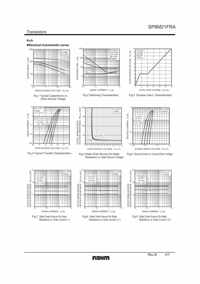
0.1 101 100
DRAIN-SOURCE VOLTAGE : VDS (V)
10
100
1000
10000
CA
PA
CIT
AN
CE
: C
(pF)
Fig.1 Typical Capacitance vs. Drain-Source Voltage
Ciss
Coss
Crss
Ta=25°Cf=1MHzVGS=0V
0.5 1.0 1.5 2.0 2.5 3.0 3.50.001
0.01
0.1
1
10
GATE-SOURCE VOLTAGE : VGS (V)
DR
AIN
CU
RR
EN
T : I
D(A
)
Fig.4 Typical Transfer Characteristics
Ta= −25°CTa=25°CTa=75°CTa=125°C
VDS= 10VPulsed
N-ch Electrical characteristic curves
0.01 0.1 1 10
DRAIN CURRENT : ID (A)
1
10
100
10000
1000
SW
ITC
HIN
G T
IME
: t (
ns)
Fig.2 Switching Characteristics
Ta=25°CVDD=25VVGS=10VRG=10ΩPulsed
td(off)
tf
td(on)
tr
Fig.3 Dynamic Input Characteristics
TOTAL GATE CHARGE : Qg (nC)
GA
TE-S
OU
RC
E V
OLT
AG
E :
VG
S(V
)
0 5 10 15 20 25 300
1
2
3
4
5
6
7
8
9
10Ta=25°CVDD=25VID=6.0ARG=10ΩPulsed
0 1 2 3 4 5 6 7 8 9 10 11 12 13 14 150
100
50
200
150
GATE-SOURCE VOLTAGE : VGS (V)
STA
TIC
DR
AIN
-SO
UR
CE
ON
-STA
TE R
ES
ISTA
NC
E :
RD
S (o
n) (m
Ω)
Fig.5 Static Drain-Source On-State Resistance vs. Gate-Source Voltage
ID=3.0A
ID=6.0A
Ta=25°CPulsed
0.0 1.00.5 1.5
SOURCE-DRAIN VOLTAGE : VSD (V)
0.01
0.1
1
10
SO
UR
CE
CU
RR
EN
T : I
S(A
)
Fig.6 Source Current vs. Source-Drain Voltage
Ta= −25°CTa=25°CTa=75°CTa=125°C
VGS=0VPulsed
0.01 10.1 10
DRAIN CURRENT : ID (A)
1
10
100
1000
STA
TIC
DR
AIN
-SO
UR
CE
ON
-STA
TE R
ES
ISTA
NC
E :
RD
S(O
N)(m
Ω)
Fig.7 Static Drain-Source On-State Resistance vs. Drain Current ( Ι )
Ta= −25°CTa=25°CTa=75°CTa=125°C
VGS=10VPulsed
0.01 10.1 10
DRAIN CURRENT : ID (A)
1
10
100
1000
STA
TIC
DR
AIN
-SO
UR
CE
ON
-STA
TE R
ES
ISTA
NC
E :
RD
S(O
N)(m
Ω)
Fig.8 Static Drain-Source On-State Resistance vs. Drain Current ( ΙΙ )
Ta= −25°CTa=25°CTa=75°CTa=125°C
VGS=4.5VPulsed
0.01 10.1 10
DRAIN CURRENT : ID (A)
1
10
100
1000
STA
TIC
DR
AIN
-SO
UR
CE
ON
-STA
TE R
ES
ISTA
NC
E :
RD
S(O
N)(m
Ω)
Fig.9 Static Drain-Source On-State Resistance vs. Drain Current ( ΙΙΙ )
Ta= −25°CTa=25°CTa=75°CTa=125°C
VGS=4VPulsed
SP8M21FRA
SP8M21Transistors
Rev.B 5/7
0.01 10.1 10
DRAIN CURRENT : ID (A)
1
10
100
1000
STA
TIC
DR
AIN
-SO
UR
CE
ON
-STA
TE R
ES
ISTA
NC
E :
RD
S(O
N)(m
Ω)
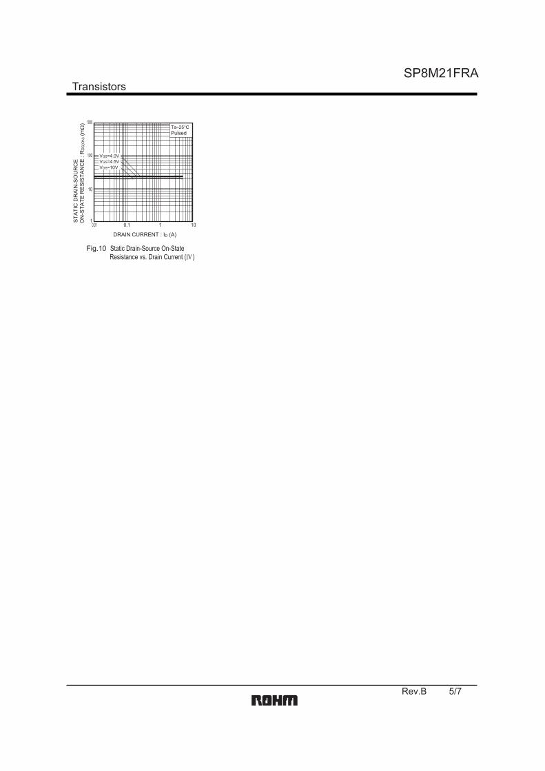
Fig.10 Static Drain-Source On-State Resistance vs. Drain Current (Ι )
VGS=10VVGS=4.5VVGS=4.0V
Ta=25°CPulsed
SP8M21FRA

SP8M21Transistors
Rev.B 6/7
0.1 101 100
DRAIN-SOURCE VOLTAGE : −VDS (V)
10
100
1000
10000
CA
PA
CIT
AN
CE
: C
(pF)
Fig.1 Typical Capacitance vs. Drain-Source Voltage
Ciss
Coss
Crss
Ta=25°Cf=1MHzVGS=0V
0.5 1.0 1.5 2.0 2.5 3.0 3.50.001
0.01
0.1
1
10
GATE-SOURCE VOLTAGE : −VGS (V)
DR
AIN
CU
RR
EN
T : −
I D(A
)
Fig.4 Typical Transfer Characteristics
Ta= −25°CTa=25°CTa=75°CTa=125°C
VDS= −10VPulsed
0.0 1.00.5 1.5
SOURCE-DRAIN VOLTAGE : −VSD (V)
0.01
0.1
1
10
SO
UR
CE
CU
RR
EN
T : −
I S(A
)
Fig.6 Source Current vs. Source-Drain Voltage
Ta= −25°CTa=25°CTa=75°CTa=125°C
VGS=0VPulsed
0 1 2 3 4 5 6 7 8 9 10 11 12 13 14 150
100
50
200
150
GATE-SOURCE VOLTAGE : −VGS (V)
STA
TIC
DR
AIN
-SO
UR
CE
ON
-STA
TE R
ES
ISTA
NC
E :
RD
S (o
n) (m
Ω)
Fig.5 Static Drain-Source On-State Resistance vs. Gate-Source Voltage
ID= −2.0A
ID= −4.0A
Ta=25°CPulsed
P-ch Electrical characteristic curves
0.01 0.1 1 10
DRAIN CURRENT : −ID (A)
1
10
100
10000
1000
SW
ITC
HIN
G T
IME
: t (
ns)
Fig.2 Switching Characteristics
Ta=25°CVDD= −25VVGS= −10VRG=10ΩPulsed
td(off)
tf
td(on)
tr
Fig.3 Dynamic Input Characteristics
TOTAL GATE CHARGE : Qg (nC)
GA
TE-S
OU
RC
E V
OLT
AG
E : −V
GS
(V)
0 5 10 15 20 3525 40300
1
2
3
4
5
6
7
8
9
10Ta=25°CVDD= −25VID= −4.0ARG=10ΩPulsed
0.01 10.1 10
DRAIN CURRENT : −ID (A)
1
10
100
1000
STA
TIC
DR
AIN
-SO
UR
CE
ON
-STA
TE R
ES
ISTA
NC
E :
RD
S(O
N)(m
Ω)
Fig.7 Static Drain-Source On-State Resistance vs. Drain Current ( Ι )
Ta= −25°CTa=25°CTa=75°CTa=125°C
VGS= −10VPulsed
0.01 10.1 10
DRAIN CURRENT : −ID (A)
1
10
100
1000
STA
TIC
DR
AIN
-SO
UR
CE
ON
-STA
TE R
ES
ISTA
NC
E :
RD
S(O
N)(m
Ω)
Fig.8 Static Drain-Source On-State Resistance vs. Drain Current ( ΙΙ )
Ta= −25°CTa=25°CTa=75°CTa=125°C
VGS= −4.5VPulsed
0.01 10.1 10
DRAIN CURRENT : −ID (A)
1
10
100
1000
STA
TIC
DR
AIN
-SO
UR
CE
ON
-STA
TE R
ES
ISTA
NC
E :
RD
S(O
N)(m
Ω)
Fig.9 Static Drain-Source On-State Resistance vs. Drain Current ( ΙΙΙ )
Ta= −25°CTa=25°CTa=75°CTa=125°C
VGS= −4VPulsed
SP8M21FRA

SP8M21Transistors
Rev.B 7/7
0.01 10.1 10
DRAIN CURRENT : −ID (A)
1
10
100
1000
STA
TIC
DR
AIN
-SO
UR
CE
ON
-STA
TE R
ES
ISTA
NC
E :
RD
S(O
N)(m
Ω)
Fig.10 Static Drain-Source On-State Resistance vs. Drain Current (Ι )
VGS= −10VVGS= −4.5VVGS= −4.0V
Ta=25°CPulsed
SP8M21FRA

DatasheetDatasheet
Notice-PAA-E Rev.001© 2015 ROHM Co., Ltd. All rights reserved.
Notice Precaution on using ROHM Products
1. If you intend to use our Products in devices requiring extremely high reliability (such as medical equipment (Note 1), aircraft/spacecraft, nuclear power controllers, etc.) and whose malfunction or failure may cause loss of human life, bodily injury or serious damage to property (“Specific Applications”), please consult with the ROHM sales representative in advance. Unless otherwise agreed in writing by ROHM in advance, ROHM shall not be in any way responsible or liable for any damages, expenses or losses incurred by you or third parties arising from the use of any ROHM’s Products for Specific Applications.
(Note1) Medical Equipment Classification of the Specific Applications JAPAN USA EU CHINA
CLASSⅢ CLASSⅢ
CLASSⅡb CLASSⅢ
CLASSⅣ CLASSⅢ
2. ROHM designs and manufactures its Products subject to strict quality control system. However, semiconductor
products can fail or malfunction at a certain rate. Please be sure to implement, at your own responsibilities, adequate safety measures including but not limited to fail-safe design against the physical injury, damage to any property, which a failure or malfunction of our Products may cause. The following are examples of safety measures:
[a] Installation of protection circuits or other protective devices to improve system safety [b] Installation of redundant circuits to reduce the impact of single or multiple circuit failure
3. Our Products are not designed under any special or extraordinary environments or conditions, as exemplified below. Accordingly, ROHM shall not be in any way responsible or liable for any damages, expenses or losses arising from the use of any ROHM’s Products under any special or extraordinary environments or conditions. If you intend to use our Products under any special or extraordinary environments or conditions (as exemplified below), your independent verification and confirmation of product performance, reliability, etc, prior to use, must be necessary:
[a] Use of our Products in any types of liquid, including water, oils, chemicals, and organic solvents [b] Use of our Products outdoors or in places where the Products are exposed to direct sunlight or dust [c] Use of our Products in places where the Products are exposed to sea wind or corrosive gases, including Cl2,
H2S, NH3, SO2, and NO2
[d] Use of our Products in places where the Products are exposed to static electricity or electromagnetic waves [e] Use of our Products in proximity to heat-producing components, plastic cords, or other flammable items [f] Sealing or coating our Products with resin or other coating materials [g] Use of our Products without cleaning residue of flux (even if you use no-clean type fluxes, cleaning residue of
flux is recommended); or Washing our Products by using water or water-soluble cleaning agents for cleaning residue after soldering
[h] Use of the Products in places subject to dew condensation
4. The Products are not subject to radiation-proof design. 5. Please verify and confirm characteristics of the final or mounted products in using the Products. 6. In particular, if a transient load (a large amount of load applied in a short period of time, such as pulse. is applied,
confirmation of performance characteristics after on-board mounting is strongly recommended. Avoid applying power exceeding normal rated power; exceeding the power rating under steady-state loading condition may negatively affect product performance and reliability.
7. De-rate Power Dissipation (Pd) depending on Ambient temperature (Ta). When used in sealed area, confirm the actual
ambient temperature. 8. Confirm that operation temperature is within the specified range described in the product specification. 9. ROHM shall not be in any way responsible or liable for failure induced under deviant condition from what is defined in
this document.
Precaution for Mounting / Circuit board design 1. When a highly active halogenous (chlorine, bromine, etc.) flux is used, the residue of flux may negatively affect product
performance and reliability. 2. In principle, the reflow soldering method must be used on a surface-mount products, the flow soldering method must
be used on a through hole mount products. If the flow soldering method is preferred on a surface-mount products, please consult with the ROHM representative in advance.
For details, please refer to ROHM Mounting specification

DatasheetDatasheet
Notice-PAA-E Rev.001© 2015 ROHM Co., Ltd. All rights reserved.
Precautions Regarding Application Examples and External Circuits 1. If change is made to the constant of an external circuit, please allow a sufficient margin considering variations of the
characteristics of the Products and external components, including transient characteristics, as well as static characteristics.
2. You agree that application notes, reference designs, and associated data and information contained in this document
are presented only as guidance for Products use. Therefore, in case you use such information, you are solely responsible for it and you must exercise your own independent verification and judgment in the use of such information contained in this document. ROHM shall not be in any way responsible or liable for any damages, expenses or losses incurred by you or third parties arising from the use of such information.
Precaution for Electrostatic
This Product is electrostatic sensitive product, which may be damaged due to electrostatic discharge. Please take proper caution in your manufacturing process and storage so that voltage exceeding the Products maximum rating will not be applied to Products. Please take special care under dry condition (e.g. Grounding of human body / equipment / solder iron, isolation from charged objects, setting of Ionizer, friction prevention and temperature / humidity control).
Precaution for Storage / Transportation 1. Product performance and soldered connections may deteriorate if the Products are stored in the places where:
[a] the Products are exposed to sea winds or corrosive gases, including Cl2, H2S, NH3, SO2, and NO2 [b] the temperature or humidity exceeds those recommended by ROHM [c] the Products are exposed to direct sunshine or condensation [d] the Products are exposed to high Electrostatic
2. Even under ROHM recommended storage condition, solderability of products out of recommended storage time period may be degraded. It is strongly recommended to confirm solderability before using Products of which storage time is exceeding the recommended storage time period.
3. Store / transport cartons in the correct direction, which is indicated on a carton with a symbol. Otherwise bent leads
may occur due to excessive stress applied when dropping of a carton. 4. Use Products within the specified time after opening a humidity barrier bag. Baking is required before using Products of
which storage time is exceeding the recommended storage time period.
Precaution for Product Label QR code printed on ROHM Products label is for ROHM’s internal use only.
Precaution for Disposition When disposing Products please dispose them properly using an authorized industry waste company.
Precaution for Foreign Exchange and Foreign Trade act Since concerned goods might be fallen under listed items of export control prescribed by Foreign exchange and Foreign trade act, please consult with ROHM in case of export.
Precaution Regarding Intellectual Property Rights 1. All information and data including but not limited to application example contained in this document is for reference
only. ROHM does not warrant that foregoing information or data will not infringe any intellectual property rights or any other rights of any third party regarding such information or data.
2. ROHM shall not have any obligations where the claims, actions or demands arising from the combination of the Products with other articles such as components, circuits, systems or external equipment (including software).
3. No license, expressly or implied, is granted hereby under any intellectual property rights or other rights of ROHM or any third parties with respect to the Products or the information contained in this document. Provided, however, that ROHM will not assert its intellectual property rights or other rights against you or your customers to the extent necessary to manufacture or sell products containing the Products, subject to the terms and conditions herein.
Other Precaution 1. This document may not be reprinted or reproduced, in whole or in part, without prior written consent of ROHM.
2. The Products may not be disassembled, converted, modified, reproduced or otherwise changed without prior written consent of ROHM.
3. In no event shall you use in any way whatsoever the Products and the related technical information contained in the Products or this document for any military purposes, including but not limited to, the development of mass-destruction weapons.
4. The proper names of companies or products described in this document are trademarks or registered trademarks of ROHM, its affiliated companies or third parties.

DatasheetDatasheet
Notice – WE Rev.001© 2015 ROHM Co., Ltd. All rights reserved.
General Precaution 1. Before you use our Pro ducts, you are requested to care fully read this document and fully understand its contents.
ROHM shall n ot be in an y way responsible or liabl e for fa ilure, malfunction or acci dent arising from the use of a ny ROHM’s Products against warning, caution or note contained in this document.
2. All information contained in this docume nt is current as of the issuing date and subj ect to change without any prior
notice. Before purchasing or using ROHM’s Products, please confirm the la test information with a ROHM sale s representative.
3. The information contained in this doc ument is provi ded on an “as is” basis and ROHM does not warrant that all
information contained in this document is accurate an d/or error-free. ROHM shall not be in an y way responsible or liable for any damages, expenses or losses incurred by you or third parties resulting from inaccuracy or errors of or concerning such information.