4g terminals: how are we going to design them?papers/compendium94-03/papers/2003/dac03/pdf... ·...
TRANSCRIPT

4G Terminals: How are We Going to Design Them? Jan Craninckx and Stéphane Donnay
IMEC Kapeldreef 75
B-3001 Leuven, Belgium Tel. +32 – 16 – 28 87 56
Email: [email protected]
ABSTRACT Fourth-generation wireless communication systems (4G) will have totally different requirements than what front-end designers have been coping with up to now. Designs must be targeted to multi-mode and reconfigurability, leading to the concept of a “software-defined radio”. A large part of such a radio will be integrated into a complex SoC, where the substrate noise coupling problem must be solved. However, for an optimal implementation of the complete system, including e.g. PA, RF filters and antenna, different technologies must be combined in a single package, merging the worlds of microwave ‘s-parameter’ designers and IC ‘spice’ designers. Design and simulation environments efficiently combining the assets of both are needed. At the same time, optimized mixed-signal radio architectures including digital compensation techniques that overcome the limitations and inaccuracies of the analog front-end must be developed. Again, efficiently designing and simulating such mixed analog/digital architectures requires an optimized tool capable of combining RF simulation techniques with digital system model simulation.
Categories and Subject Descriptors B.7.m [Integrated Circuits]: Miscellaneous.
General Terms Design, Performance.
Keywords Telecommunication, Wireless systems, 4th Generation, Radio Front-end
1. INTRODUCTION The statement “The world is going wireless” is already quite a number of years old. Second generation (2G) systems such as GSM were a worldwide success and turned the cellular phone into a commodity for the average consumer. New applications require higher datarates that are at the moment provided by 2.5G
extensions. The real thing required for applications such as wireless gaming and video however will be third generation (3G) systems [1]. Although not rolling out as fast as expected due to the worldwide market downturn, it is a fact that in a few years our life will again have drastically changed, and the fact of taking a wireless video call will no longer astonish us. Another development in the wireless telecommunication area in recent years is the arrival of wireless LAN systems. The first major player here is the IEEE 802.11b standard, delivering up to 11Mb/s, but the major breakthrough is believed to come with 802.11a systems, which employ OFDM modulation in the 5GHz ISM band to provide up to 54Mb/s [2]. Contrary to cellular systems, which provide moderate data rate at high mobility, a WLAN aims to deliver high data rates at limited mobility. And yes, now is the time to think about fourth generation (4G) systems. They will not be a revolution in technology, but more an evolution where the user is in the central position. New services and applications will emerge, and new business models will be developed [3]. In this new wireless world, depicted in Fig. 1, the user will be able to interact at several levels with several objects. A Wireless Body Area Network (WBAN) will consist of e.g. wearable devices, sensors monitoring our health, etc. Ad hoc networks are set up with other persons or appliances in our neighborhood. High-speed data links are provided by Wireless Local Area Networks, but only in home of office environments and at a number of hot spots, e.g. in airports. Global coverage for connection to the rest of the world happens over the radio access link of a cellular or satellite network.
WBAN
WLANCellularnetwork
Satellite
network
Ad-hocnetwork
WBAN
WLANWLANCellularnetwork
CellularnetworkSatellite
network
Satellite
network
Ad-hocnetwork
Fig. 1. A view on the new wireless world
This leads to the current view on what a 4th generation wireless terminal should look like. We will communicate over varying distances and varying bitrates with a broad range of applications and persons. The air interface we will use will depend on the instantaneous requirements: low-power, low-datarate systems for
Permission to make digital or hard copies of all or part of this work for personal or classroom use is granted without fee provided that copies are not made or distributed for profit or commercial advantage and that copies bear this notice and the full citation on the first page. To copy otherwise, or republish, to post on servers or to redistribute to lists, requires prior specific permission and/or a fee. DAC 2003, June 2-6, 2003, Anaheim, California, USA. Copyright 2003 ACM 1-58113-688-9/03/0006…$5.00.
79
6.3
the WBAN, global coverage and medium datarates for cellular systems, local coverage and high datarates for WLAN. The wireless terminal should be compliant to all (or a large subset of) current existing standards to provide backwards compatibility. New air interfaces might be developed that employ reconfigurable coding and modulation schemes and multi-antenna techniques that adapt to the circumstances to provide optimal communication. The limitations of a certain air interface and the transitions between them should be transparent for the user.
Fig. 2. Overview of wireless standards
For the radio front-end, this presents several design challenges. A large number of standards must be served: from low-power body area networks and cellular standards (GSM/UMTS), over personal networks (such as Bluetooth) to high datarate wireless LANs with multiple-antenna (MIMO: multiple-input multiple-output) extensions. Making a terminal that contains an RF front-end for every possible standard (and even multiple front-ends for multiple-antenna systems) is not feasible because of the required cost and form factor. Moreover, it is not a flexible approach w.r.t. new and emerging air interfaces. Mobile users will only be able to benefit from this new wireless world if they are equipped with a single (or a limited number of) reconfigurable multi-mode multi-band front-end(s). Such a front-end is also referred to as a Software Defined Radio (SDR) [3],[4]. In the following sections, several key aspects and design challenges in the development of a SDR are discussed. The focus is only the analog and RF part of the radio; the challenges in e.g. the digital modulation/demodulation and the MAC layer are beyond the scope of this paper. Section 2 discusses system-on-chip (SoC) integration issues, where substrate noise problems will be a major challenge. Since SoC will have its limits, the optimal choice for an SDR will be a system-in-a-package (SiP) approach. Technology and design tool issues in this area are treated in section 3. Section 4 discusses the impact of the SDR requirements on the front-end building blocks. Because analog reconfigurability comes at a certain cost, we expect that digital correction loops will be widely used to compensate for analog non-idealities. Section 5 discusses a high-level mixed-mode simulation tool that is indispensable in the design of such systems. Finally, section 6 presents some conclusions.
2. SYSTEM-ON-CHIP INTEGRATION The most important way to lower the cost of consumer communication products in the past decades, has been to reduce the number of components and integrate more and more system functions on a single IC. In the end of the ‘90s, the SoC approach was advocated by many players in the field. The research in (and progress of) RF CMOS circuits [5]-[7] opened up the possibility
to integrate the complete front-end of e.g. a GSM system with the digital baseband processor, which was one of the last major steps to take towards a single-chip mobile phone. The Bluetooth standard [8] was even conceived with integration as a SoC in mind. It is of course not yet clear how far the SoC approach will work for an SDR, but probably also here a lot of the analog circuitry will be implemented in an advanced CMOS technology together with the digital processing blocks. A major challenge to take in the design of such a mixed-signal IC will be the integrity of the analog circuits in the presence of digital switching noise. Although a number of commercial tools allow the designer to analyze the impact of substrate noise on the performance of embedded analog circuits in detail, it is not always easy to determine a model for the digital switching noise generated by a complex digital system of several 100k gates. To determine the noise generated by the digital part, circuit-level simulations of this part, completed with a substrate model are only feasible for very small digital circuits. A macro-modeling approach that represents the complete digital part as e.g. one big inverter [9] gives only a very crude estimation. Another approach that uses a macromodel for every standard cell in a digital circuit, is the substrate noise simulation methodology shown in Fig. 3 [10]. This methodology that has been elaborated originally for low-ohmic substrates, consists of three parts. The first part is the library characterization that must be performed once for each new technology. During the library characterization, a substrate noise macro model is created for every standard cell, and the noise injection currents are extracted for every possible switching activity for every standard cell. The standard VHDL gate-level simulation library is also extended to enable the extraction of all switching events during a normal VHDL gate-level simulation.
Fig. 3. Substrate noise waveform simulation methodology
The second part of the methodology starts with a given gate-level netlist of a digital design. From this netlist, a chip-level simulation model is created, using the previously extracted macro models for each separate gate. A model for the package parasitics is also added to the chip-level simulation model. Next, the gate-level netlist is used in a normal gate-level simulation, using the extended simulation library. The output of this simulation is a listing with all switching events. These switching events are used to calculate the total noise current waveform, using the current waveforms extracted in step one for each individual gate.
80

The third part of the methodology is the actual simulation of the voltage of the substrate back node (low-ohmic substrates) due to the switching noise. This is done by combining the chip-level simulation model with the total noise current sources, and solving this circuit with, for example, a SPICE simulator, to obtain the substrate noise voltage. This macro-modelling approach allows the designer to predict the noise generated by complex digital systems in strongly reduced simulation times with excellent agreement with measurements [11].
3. SYSTEM-IN-A-PACKAGE INTEGRATION
Although complete systems on a (CMOS) chip appear to be the holy grail for many researchers, the economical reality of a SoC is however not completely clear. The expensive analog and RF process options increase the cost per mm2 of the IC, and they are not used in the major digital part. The same argument applies to the extra process steps needed for the integration of e.g. flash memory in the SoC. The power consumption of the RF circuits might have been less if another technology (e.g. SiGe BiCMOS) was used. Moreover if digital technology shrinks, it takes too long to redesign the analog blocks, especially if several redesigns are required. The longer design time of a SoC might cause you to miss the market window. Also yield, packaging and test issues will have their impact on the total cost. And some building blocks such as the power amplifier and the antenna switch still cannot be integrated, so the system of a SoC is not yet complete. For 4th generation terminals, feasibility will again become an issue. The performances of analog circuits will be stretched even further than now because of the required reconfigurability. Inevitably, since building blocks can no longer be optimized for one certain set of specifications, a cost will have to be paid in terms of power consumption, noise performance, area, etc. To limit this cost, or even ensure the feasibility of the circuit, probably the best available technology must be used, and high-quality passive external components might be needed. This has lead to a major shift in interest towards system-in-a-package integration. With such an approach all the building blocks of the system can be implemented in their optimal technology of choice. High-quality passive components are available to improve the performance of the analog circuits. The package can now include really all required blocks, including power amplifier, antenna switch, antenna filter and even the antenna itself. We believe that this approach can lead to a feasible and even optimal implementation of a software-defined radio, including the digital processing blocks.
3.1 SIP TECHNOLOGY MCM technology provides a common carrier onto which different ICs can be combined. A thin-film MCM technology (MCM-D) starts with a very low loss substrate such as glass, onto which several layers (conductors, dielectric materials, …) are processed in a similar fashion as the back-end technology for IC processing. RF ICs are mounted with a flip-chip technique to reduce the signal degradation due to bonding wired inductance. Passive components include thin-film resistors, high-quality inductors and capacitors [12]. These can be used to integrate RF bandpass filters or impedance matching networks, or to improve the performance of certain blocks such as oscillators [13].
Not all components profit optimally from the MCM technology. The power amplifier e.g. suffers from the low thermal conductivity of the glass substrate. Also the antenna design requires a dielectric thickness much larger than available on MCM. However, as the MCM-substrate has to be packaged in e.g. a BGA anyway, this laminate packaging technology brings also a solution for the integration of PA and antenna. As a demonstrator, we have integrated a GaAs PA, a GaAs TX/RX switch, high-quality RF MCM-D filters, a BiCMOS IC containing an LNA and a PPA together with a patch antenna [14]. All ICs and filters are contained in the MCM, which is placed in a cavity in the BGA and connected with very short bonding wires to the PA and the antenna. The antenna laminate encapsulates the BGA, as shown in Fig. 4. A photograph of the realised structure (before closing the top) is shown in Fig. 5.
Fig. 4. Cross section of the complete BGA package
Fig. 5. Photograph of the BGA package
In the coming years, SiP technology will without any doubt evolve even further. Micro Electrical-Mechanical Structures (MEMS) could be added, and they will allow to include new functionalities (such as a TX/RX switch), or to improve the performance of front-end building blocks with e.g. a MEMS varicap or a very selective bandpass filter [15].
3.2 SIP DESIGN TOOL ISSUES The design of a SiP however requires also special design tool capabilities. The system level design space has again increased with an extra dimension, and the correct trade-offs must be made for the optimal choice of building block technology and
81

specifications. A first order radio link budget that distributes noise, linearity, filtering and gain over the RX and TX chain is still done with hand calculations. Most designers still use a spreadsheet tool to implement this. This is on one hand not very “modern” and even error-prone, but on the other hand allows the system level designer to quickly tune the spreadsheet to his proper needs. Accurate cost models for the various components are also required for these system-level trade-offs. How much will an extra MCM component influence the system cost, or how much does the somewhat worse performance of an inductor integrated on the IC impact the price the customer wants to pay? These trade-offs are now done in the early stage of the design feasibility based on previous experience or capability. A co-simulation or co-design environment should allow fast evaluation of the several options to take. A bridge must also be built between the traditional microwave “s-parameter” design techniques and the “spice” approach taken by the IC designers. These two worlds differ in language and tools, and both have their advantages in the applications they are used in. An analog designer reasons with voltages and currents, which is very convenient for designing an IC, but doesn’t work at all to develop an impedance matching network. With a Smith chart however, this becomes a trivial problem. The MCM-D technology offers a library of passive components, which have been measured and accurately characterised with s-parameters. These must however be included in the simulations of active building blocks, which use other simulation techniques such as the widely used transient-based shooting method of SpectreRF [16]. To include s-parameter blocks or transmission lines in transient-based simulators, an extra modelling step is required to convert them into an equivalent N-port model or RLC network. Also the new SiP components such as MEMS add a mechanical dimension to the modelling and simulation problem. Accurate simulation based on the physics of the component under consideration requires the solution of partial differential equations. This however does not yield interpretable models and increases simulation time. Alternative approaches must be developed that provide more efficient models without loss in accuracy [17].
4. RECONFIGURABLE BUILDING BLOCKS
The requirements of the varying communication standards differ over a very wide range in terms of center frequency, signal bandwidth, signal-to-noise ratio, linearity, etc. This will have its impact on all building blocks of a radio front-end, which can be grouped as:
- Antenna with antenna filter - RF amplification (LNA in receive, PA in transmit) - Frequency translation to/from a certain IF (which could be
(almost) zero) - Amplification and/or filtering at IF - D/A and A/D conversion
The following paragraphs shortly discuss some key issues. A major hurdle to take in the flexible radio design will be the antenna and the antenna filter. Current antenna performance is generally optimized for narrow band operation and maximum
blocking of out-of-band signals. In a 4G terminal, the carrier frequency will vary from below 1GHz up to 6GHz. One obvious way of proceeding is of course to use several antenna, each tuned to a specific band. As this will result in a large form factor, wideband, multi-band [18] or tunable [19] antenna designs are preferred. Also the antenna filter will suffer from the same problem. It should definitely be tunable in center frequency, something that might be obtained with RF MEMS integrated in the MCM technology. RF amplification in the receive path is performed by the low-noise amplifier (LNA). Current implementations mostly use an inductively degenerated input stage to provide impedance matching and a tuned output stage [20]. Broadband LNA designs cannot apply these techniques, unless again some kind of frequency tuning is employed [21]. On top of that, some flexibility must be incorporated to trade off noise, linearity and power consumption for each application. These requirements will inevitably result in a performance degradation. The story for power amplifiers (PA) is even more difficult. Also here, amplifier classes with high efficiency require narrowband tuned output networks, and extending this to broadband designs might turn out to be impossible. Also the output power requirements for each standard are different. So very likely the SDR will contain several PAs to cover all frequency bands. This multiplexing approach LNAs and PAs is the one used in most multi-band transceiver designs published today [22]. Frequency synthesis for SDR is complicated by the large variations in carrier frequency. A single VCO can only have a limited tuning range, so up to now only one band could be covered, although sometimes convenient frequency division can be exploited if two bands are a factor two apart. To cover more bands with a single synthesizer, the frequency division concept could be expanded further, and combined with frequency multiplication and/or harmonic mixing [23]. Quadrature generation for image-reject mixers poses another challenge, as the polyphase networks usually employed do not operate in a wide frequency range [24]. IF (or baseband) signal processing constraints also vary widely with signal levels and bandwidths. A reconfigurable channel select filter requires very wide frequency tuning, which can be done by varying the value of capacitors, resistors, and/or transconductances. And last but not least, also in A-to-D and D-to-A architectures, novel principles will have to be employed to achieve optimal performance for the required signal. Probably the most elegant solution will come from oversampled converters, which can even take over some of the functionality of the channel select filters [25].
5. SYSTEM-LEVEL ANALOG/DIGITAL TRADE-OFFS
The amount of digital signal processing is also steadily growing in modern telecom systems. The digital world offers a higher flexibility compared to analog blocks, and can – at least partially – compensate some of the signal impairments caused by analog front-end blocks. As an example, digital signal processing can compensate insufficient analog quadrature matching in the zero-IF receiver of a high-speed WLAN. Even low-frequency common phase noise on the OFDM carriers can be estimated and
82
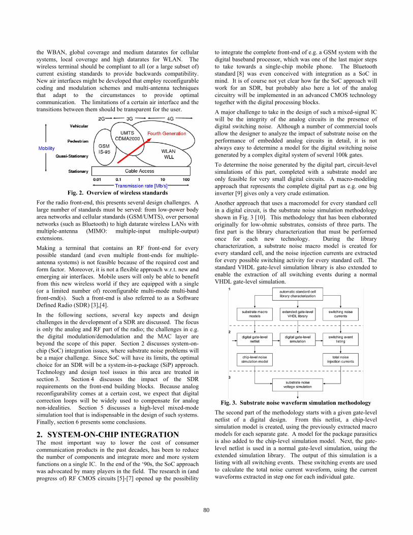
compensated for [30]. Fig. 6 shows the influence of a 10%/10º quadrature mismatch (IQ) and –32dBc integrated phase noise (PN) in the BER of a 64QAM coded OFDM signal, and the improvement obtained by the digital compensation techniques.
Fig. 6. BER improvement by digital compensation techniques To predict the effectiveness of complicated digital compensation algorithms, and the effect of analog non-idealities such a phase noise, linearity and mismatch, the analog and the digital blocks need to be simulated together. The traditional analog/digital mixed-mode simulation problems are increased with an order of magnitude because of the high frequencies used in the analog RF blocks. High-level simulations that support architectural studies of mixed-signal telecom front-ends most often require the co-simulation of three parts:
- a digital part, which in this phase is typically modeled as a dataflow system, either in floating point or fixed-point representation;
- an analog part operating at RF frequencies; - an analog part operating at lower frequencies (IF or baseband).
To simulate the bit-error-rate (BER) of a complete telecom link, a very efficient simulation engine is required, since a lot of information (corresponding to many experiments in a Monte-Carlo approach) has to be sent through that link. Our high-level co-simulation methodology is based on two existing C++ based tools: OCAPI, optimized for digital VLSI signal processing [26], and FAST, which has been optimized for the description of nonlinear analog models [27]. An interfacing layer couples the kernels of FAST and OCAPI, which both use dataflow scheduling. With FAST, the analog blocks are translated before simulation into a computational graph, which is an equivalent digital dataflow representation. A simulation is then nothing else but an evaluation of that computational graph. First high-level models for the analog blocks for architectural exploration are very rough and could be generated by hand. More accurate models can be generated by analyzing a spice-like netlist using approaches such as [28]. This methodology splits the nonlinear behavior of the total circuit into different contributions using Volterra series. In this way, insight into the nonlinear operation of a circuit as well as high-level models is obtained. An example for an LNA is shown in Fig. 7.
R1
T1
R2T2
R3
T3
L
C
Vcc
In OutR1
T1
R2T2
R3
T3
L
C
Vcc
In Out
inputoutput
K2gm3Hb(s) x2
(s)Ha
Hc(s)Hd(s)
K3gm3x3
++
inputoutput
K2gm3Hb(s) x2
(s)Ha
Hc(s)Hc(s)Hd(s)
K3gm3x3
++
Fig. 7. Low-noise amplifier and its high-level model
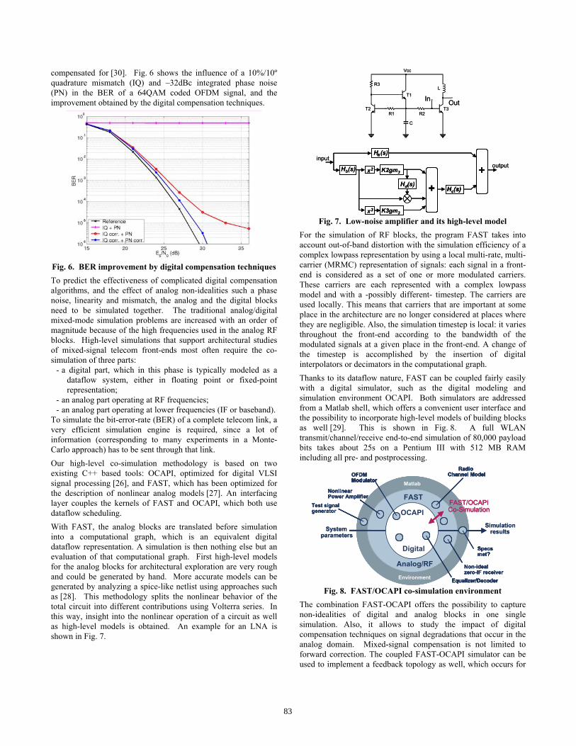
For the simulation of RF blocks, the program FAST takes into account out-of-band distortion with the simulation efficiency of a complex lowpass representation by using a local multi-rate, multi-carrier (MRMC) representation of signals: each signal in a front-end is considered as a set of one or more modulated carriers. These carriers are each represented with a complex lowpass model and with a -possibly different- timestep. The carriers are used locally. This means that carriers that are important at some place in the architecture are no longer considered at places where they are negligible. Also, the simulation timestep is local: it varies throughout the front-end according to the bandwidth of the modulated signals at a given place in the front-end. A change of the timestep is accomplished by the insertion of digital interpolators or decimators in the computational graph. Thanks to its dataflow nature, FAST can be coupled fairly easily with a digital simulator, such as the digital modeling and simulation environment OCAPI. Both simulators are addressed from a Matlab shell, which offers a convenient user interface and the possibility to incorporate high-level models of building blocks as well [29]. This is shown in Fig. 8. A full WLAN transmit/channel/receive end-to-end simulation of 80,000 payload bits takes about 25s on a Pentium III with 512 MB RAM including all pre- and postprocessing.
Matlab
Environment
FAST
Analog/RF
Systemparameters
Simulationresults
OCAPI
Digital
NonlinearPower Amplifier
ModulatorOFDMModulator
Test signalgenerator
Non-idealzero-IF receiver
Specsmet?
Equalizer/Decoder
Radio Channel Model
FAST/OCAPICo-Simulation
Matlab
Environment
Matlab
Environment
FAST
Analog/RF
FAST
Analog/RF
Systemparameters
Simulationresults
OCAPI
Digital
OCAPI
Digital
NonlinearPower AmplifierNonlinearPower Amplifier
ModulatorOFDMModulatorModulatorOFDMModulator
Test signalgeneratorTest signalgenerator
Non-idealzero-IF receiver
Specsmet?
Equalizer/Decoder
Radio Channel Model
Non-idealzero-IF receiver
Specsmet?
Equalizer/Decoder
Radio Channel Model
Specsmet?
Equalizer/Decoder
Radio Channel Model
Equalizer/Decoder
Radio Channel Model
FAST/OCAPICo-SimulationFAST/OCAPICo-Simulation
Fig. 8. FAST/OCAPI co-simulation environment
The combination FAST-OCAPI offers the possibility to capture non-idealities of digital and analog blocks in one single simulation. Also, it allows to study the impact of digital compensation techniques on signal degradations that occur in the analog domain. Mixed-signal compensation is not limited to forward correction. The coupled FAST-OCAPI simulator can be used to implement a feedback topology as well, which occurs for
83

example in automatic gain control or DC offset compensation loops. The high simulation speed allows to efficiently explore the design space for optimal solutions.
6. CONCLUSIONS In this paper, we have tried to project a view on 4th generation wireless terminals and the impact their requirements have on RF front-end designers and their tools. SoC integration will suffer from substrate noise problems, and cannot offer the feasibility of a complete system. SiP technology adds another degree of freedom, and will allow to make a better trade-off between passive components, RF IC technology and digital signal processing. High-level simulation tools are required that allow to quickly explore the broad range of architecture-level analog-digital trade-offs.
7. REFERENCES [1] 3GPP TS 25.201, “Physical layer – general description” [2] IEEE standard 802.11a: Wireless MAC and PHY
specifications, “High-speed physical layer in the 5GHz band”, IEEE, New York, 2000
[3] Wireless World Research Forum, “Book of visions 2001”, http://www.ww-rf.org
[4] SDR Forum, http://www.sdrforum.org [5] M. Steyaert, J. Janssens, B. De Muer, M. Borremans, and
N. Itoh, “A 2V CMOS cellular transceiver frontend”, ISSCC 2000 Digest of Technical Papers, pp. 142-143
[6] A. Rofougaran et al., “A single-chip 900-MHz spread-spectrum wireless transceiver in 1-µm CMOS”, IEEE Journal of Solid-State Circuits, vol. 33, no. 4, pp. 515-547, April 1998
[7] T. Lee, “The design of CMOS radio-frequency integrated circuits”, Cambridge University Press, ISBN 0-521-63922-0, 1998
[8] The Bluetooth standard, http://www.bluetooth.com [9] P. Van Zeijl, “A practical approach to modeling silicon-
crosstalk in systems-on-silicon”, chapter 9 of “Substrate noise coupling in mixed-signal ASICs”, S. Donnay and G. Gielen, edts, Kluwer Academic Publishers, 2003.
[10] M. van Heijningen, M. Badaroglu, S. Donnay, M. Engels, and I. Bolsens, “High-level simulation of substrate noise generation including power supply noise coupling”, Proc. 37th Design Automation Conference, pp. 446-451, June 2000.
[11] M. Badaroglu et al., “Modeling and experimental verification of substrate noise generation in a 220kGates WLAN system-on-chip with multiple supplies," IEEE Journal of Solid-State Circuits, vol. 38, no. 7, July 2003.
[12] S. Donnay et al., “Chip-package co-design of a low-power 5GHz RF front-end”, Procedings of the IEEE, vol. 88, no. 10, pp. 1583-1597, Oct. 2000
[13] M. Innocent, P. Wambacq, S. Donnay, H. A. C. Tilmans, H. De Man, and W. Sansen, “MEMS variable capacitor versus MOS variable capacitor for a 5GHz voltage controlled oscillator”, Proc. of European Solid-State Circuits Conference, pp. 487-490, Sept. 2002
[14] J. Ryckaert et al., “Single-package 5GHz WLAN RF module with embedded patch antenna and 20dBm power amplifier”, IEEE International Microwave Symposium, June 2003
[15] C. Nguyen, L. Katehi and G. Rebeiz, “Micromachined devices for wireless communications”, Proceedings of the IEEE, vol. 86, no. 8, pp. 1756-1768, Aug. 1998.
[16] Cadence, “Affirma RF simulator (spectreRF) user guide” [17] M. Innocent, P. Wambacq, S. Donnay, H. Tilmans,
W. Sansen, and H. De Man, “An Analytic Volterra-Series-Based Model for a MEMS Variable Capacitor”, IEEE Trans. On Computer-Aided Design of Integrated Circuits and Systems, vol. 22, no. 2, pp. 124-131, Feb. 2003
[18] C. Puente-Baliarda, J. Romeu, R. Pous, and A. Cardama, “On the behavior of the Sierpinski multiband fractal antenna”, IEEE Transactions on Antennas and Propagation, vol. 46, no. 4, pp. 517-524, April 1998
[19] O. Rostbakken, G.S. Hilton, and C.J. Railton, “An adaptive microstrip patch antenna for use in portable transceivers”, IEEE 46th Vehicular Technology Conference, vol. 1, pp. 339-343, April 1996.
[20] J. Janssens and M. Steyaert, “CMOS cellular receiver front-ends from specification to realization”, Kluwer Academic Publishers, ISBN 0-7923-7637-4, Jan. 2002
[21] P.-W. Lee, H.-W. Chiu, T.-L. Hsieh, C.-H. Shen, G.-W. Huang, and S.-S. Lu, “A SiGe low noise amplifier for 2.4/5.2/5.7GHz WLAN applications”, ISSCC 2003 Digest of Technical Papers, pp. 364-365
[22] R. Magoon, A. Molnar, J. Zachan, G. Hatcher, and W. Rhee, “A single-chip quad-band (850/900/1800/1900 MHz) direct conversion GSM/GPRS RF transceiver with integrated VCO and fractional-N synthesizer”, IEEE Journal of Solid-State Circuits, vol. 37, no. 12, pp. 1710-1720, Dec 2002
[23] T. Yamaji, H. Tanimoto, and H. Kokatsu, “An I/Q active balanced harmonic mixer with IM2 cancellers and a 45º phase shifter”, IEEE Journal of Solid-State Circuits, vol. 33, no. 12, pp. 2240-2246, Dec 1998
[24] F. Behbahani, Y. Kishigami, J. Leete, and A. Abidi, “CMOS mixers and polyphase filters for large image rejection”, IEEE Journal of Solid-State Circuits, vol. 36, no. 6, pp. 873-887, June 2001
[25] R. van Veldhoven, “A tri-mode continuous-time Σ∆ modulator with switched-capacitor feedback DAC for a GSM-EDGE/CDMA200/UMTS receiver”, ISSCC 2003 Digest of Technical Papers, pp. 60-61
[26] P. Schaumont et al., “A programming environment for the design of complex high speed ASICs”, Proc. Design Automation Conference, pp. 315-320, June 1998.
[27] P. Wambacq et al., “Dataflow simulation of mixed-signal communication circuits using a local multirate, multicarrier signal representation”, IEEE Transactions on Circuits and Systems I: Fundamental Theory and Applications, vol. 49, no. 11, pp. 1554-1562, Nov. 2002
[28] P. Wambacq, P. Dobrovolny, S. Donnay, M. Engels, and I. Bolsens, “Compact modeling of nonlinear distortion in analog communication circuits”, Design Automation and Test in Europe (DATE), pp. 350-354, March 2000.
[29] W. Eberle, G. Vandersteen, P. Wambacq, S. Donnay, G. Gielen, and H. De Man, “Behavioral modeling and simulation of a mixed analog/digital automatic gain control loop in a 5 GHz WLAN receiver”, Design Automation and Test in Europe (DATE), pp. 642-647, March 2003.
[30] J. Tubbax, B. Come, L. Van der Perre, S. Donnay, and M. Engels, “Joint Compensation of IQ Imbalance and Phase Noise”, IEEE semi-annual Vehicular Technology Conference, April 2003
84