4493x a71ch sds - farnell.com · 12nc type number development kit description 935368997598...
TRANSCRIPT
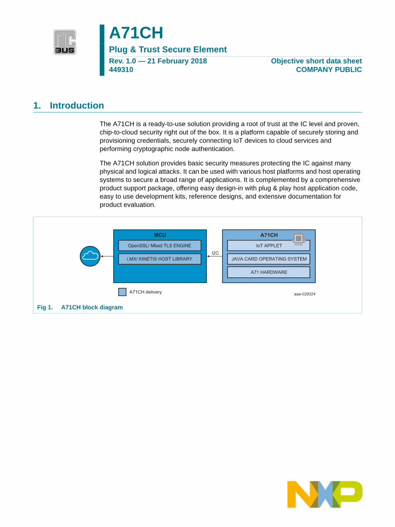
1. Introduction
The A71CH is a ready-to-use solution providing a root of trust at the IC level and proven, chip-to-cloud security right out of the box. It is a platform capable of securely storing and provisioning credentials, securely connecting IoT devices to cloud services and performing cryptographic node authentication.
The A71CH solution provides basic security measures protecting the IC against many physical and logical attacks. It can be used with various host platforms and host operating systems to secure a broad range of applications. It is complemented by a comprehensive product support package, offering easy design-in with plug & play host application code, easy to use development kits, reference designs, and extensive documentation for product evaluation.
A71CHPlug & Trust Secure ElementRev. 1.0 — 21 February 2018 449310
Objective short data sheet COMPANY PUBLIC
Fig 1. A71CH block diagram
aaa-029324
OpenSSL/ Mbed TLS ENGINE
i.MX/ KINETIS HOST LIBRARY
A71CH delivery
IoT APPLET
A71CHMCU
I2CJAVA CARD OPERATING SYSTEM
A71 HARDWARE
NXP Semiconductors A71CHPlug & Trust Secure Element
2. General description
2.1 A71CH naming conventions
The following table explains the naming conventions of the commercial product name of the A71CH products. Every A71CH product gets assigned such a commercial name, which includes also customer and application specific data.
The A71CH commercial names have the following format.
A71CHxagpp(p)/mvsrrff
The ‘A71CH’ is a constant, all other letters are variables, which are explained in Table 1.
2.2 I2C interface
The A71CH has an I2C interface in slave mode, supporting data rates up to 400 kbit/s operating in Fast-Mode (FM). The I2C interface is using the Smartcard I2C protocol as defined in Ref. 3 which is based on SMBus.
More information about I2C address used during A71CH implementation can be found in Ref. 4; the default I2C address after power-on-reset is 0x90 for Write, and 0x91 for Read.
2.3 Security licensing
NXP Semiconductors has obtained a patent license for SPA and DPA countermeasuresfrom Cryptography Research Incorporated (CRI). This license covers both hardware andsoftware countermeasures. It is important to customers that countermeasures within theoperation system are covered under this license agreement with CRI. Further details can be obtained on request.
Table 1. A71CH commercial name format
Variable Meaning Values Description
x IC hardware specification code
1 standard operational ambient temperature: −25 °C to +90 °C I2C interface supported
2 standard operational ambient temperature: −40 °C to +90 °C I2C interface supported
a embedded operating system code
C Java card operating system
g embedded application firmware (applet) code
H H is a fixed value = IoT security applet pre installed
pp(p) package type code dd(d)= Delivery Type, TK2= HVSON8 (4x4), UK= WLCSP12
m Manufacturing Site Code T
v Silicon Version Code 0
s Silicon Version Subcode B
rr ROM Code ID
ff FabKey ID
449310 All information provided in this document is subject to legal disclaimers. © NXP B.V. 2018. All rights reserved.
Objective short data sheet COMPANY PUBLIC
Rev. 1.0 — 21 February 2018449310 2 of 23

NXP Semiconductors A71CHPlug & Trust Secure Element
3. Features and benefits
3.1 Key benefits
Secure, zero-touch connectivity
End-to-end security, from chip to edge to cloud
Secure credential injection for IC-level root of trust
Fast design-in with complete product support package
Easy to integrate with different MCU platforms
3.2 Security features
The A71CH security concepts includes many security measures to protect the chip.
The A71CH operates fully autonomously based on an integrated Javacard operating system and applet. Direct memory access is possible by the fixed functionalities of the applet only. With that, the content from the memory is fully isolated from the host system.
Attack protection by integrated design measures in the chip layout, the logic and the functional blocks.
3.3 Cryptography features
The A71CH Secure Element provides the following functionality:
Protected Access storage, generation, insertion or deletion of 4 key pairs (ECC NIST P-256)
Systematic enforced authentication
Secure key management
Protected Access storage, insertion or deletion of 3 public keys
Signature generation and verification (ECDSA)
Shared secret calculation for Key Agreement (ECDH or ECDH-E)
Protected Access storage and use of 2 monotonic counters (32 bits each)
Protected Access storage, insertion or deletion of symmetric secrets (8x 128 bits); longer keys can be used by using a ConstructedSecret type
Content protected access to keys
A unique chip ID (18 bytes)
HKDF key derivation using the symmetric secrets as key, Extract & Expand or Expand only modes
HMAC SHA256 calculation in one shot or sequential
Freezing of credentials (= OTP behavior)
Secure channel SCPO3 GP support
(Optional) trust provisioning of key pairs, public keys, symmetric secrets, etc.
Possibility to lock the A71CH module as transport lock mechanism
ECC keys and operations support the following ECC curve:
NIST P-256
449310 All information provided in this document is subject to legal disclaimers. © NXP B.V. 2018. All rights reserved.
Objective short data sheet COMPANY PUBLIC
Rev. 1.0 — 21 February 2018449310 3 of 23

NXP Semiconductors A71CHPlug & Trust Secure Element
3.4 Functional features
Dedicated MX51 security CPU
400 kbit/s I2C Fast-mode interface
−40 °C to +90 °C operational ambient temperature (A7102)
On-chip Javacard operating system
40 μA typical sleep mode current with I2C pads in tristate mode
10 μA max deep sleep mode current with I2C pads in tristate mode
High-performance Public Key Infrastructure (PKI)
EEPROM with min 500,000 cycles endurance and min 25 years retention time
HVSON8 package
449310 All information provided in this document is subject to legal disclaimers. © NXP B.V. 2018. All rights reserved.
Objective short data sheet COMPANY PUBLIC
Rev. 1.0 — 21 February 2018449310 4 of 23
NXP Semiconductors A71CHPlug & Trust Secure Element
4. Applications
4.1 Use Cases and target applications
A710xCH EXAMPLE USE CASES
Secure connection to public/private clouds, edge computing platforms, infrastructure
Secure Amazon Web Services-compliant connectivity
Secure commissioning
Device-to-device authentication
Proof of origin / anti-counterfeiting
Key storage and data protection
Secure provisioning of credentials
Ecosystem protection
A710xCH TARGET APPLICATIONS
Connected industrial devices
Sensor networks
IP cameras
Home gateways
Home appliances
449310 All information provided in this document is subject to legal disclaimers. © NXP B.V. 2018. All rights reserved.
Objective short data sheet COMPANY PUBLIC
Rev. 1.0 — 21 February 2018449310 5 of 23

NXP Semiconductors A71CHPlug & Trust Secure Element
5. Ordering information
5.1 Ordering options
[1] a = A or C, g = G, C or A, according to the A71CH type classification see Section 2.1 “A71CH naming conventions”
Table 5 gives an overview of available A71CH product types.
[1] g = G, C, or A; pp(p) = UA or HN1, according the A71CH type classification see Section 2.1 “A71CH naming conventions”
5.1.1 Samples and final products
Section 5.1.2, gives details of how to order samples and final products.
5.1.2 Ordering A71CH samples
Samples can be ordered from NXP Semiconductors via nxp.com using the "Buy Direct" button.
Note that NXP Semiconductors can provide up to 5 pieces free of charge. Larger quantities have to be ordered separately.
Table 2. Ordering information
Type number[1] Package
Name Description Version
A7101agTK2/... HVSON-8 plastic thermal enhanced very thin small outline package; no leads; 8 terminals; body 4 × 4 × 0.85 mm
SOT909-1
A7102agTK2/...
Table 3. A71CH type table
12NC Type number Product Package
9353 68 097118 A7101CHTK2/T0BC2V6 A71(01)CH HVSON8
9353 635 15118 A7102CHTK2/T0BC2A5 A71(02)CH HVSON8
Table 4. A71CH type table
12NC Type number Development kit Description
935368997598 OM3710/A71CHARD OM3710/A71CHARD Arduino compatible development kit
935369302598 OM3710/A71CHPCB OM3710/A71CHPCB Mini PCP
OM3710/B001 I2C Bird
Table 5. A71CH feature table
Product type[1] Operational ambient temperature Interface option
A7101Cgpp(p) −25 °C to +90 °C I2C
A7102Cgpp(p) −40 °C to +90 °C
449310 All information provided in this document is subject to legal disclaimers. © NXP B.V. 2018. All rights reserved.
Objective short data sheet COMPANY PUBLIC
Rev. 1.0 — 21 February 2018449310 6 of 23
NXP Semiconductors A71CHPlug & Trust Secure Element
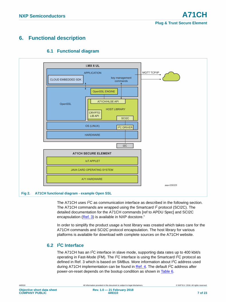
6. Functional description
6.1 Functional diagram
The A71CH uses I2C as communication interface as described in the following section. The A71CH commands are wrapped using the Smartcard I2 protocol (SCI2C). The detailed documentation for the A71CH commands [ref to APDU Spec] and SCI2C encapsulation (Ref. 3) is available in NXP docstore.”
In order to simplify the product usage a host library was created which takes care for the A71CH commands and SCI2C protocol encapsulation. The host library for various platforms is available for download with complete sources on the A71CH website.
6.2 I2C Interface
The A71CH has an I2C interface in slave mode, supporting data rates up to 400 kbit/s operating in Fast-Mode (FM). The I2C interface is using the Smartcard I2C protocol as defined in Ref. 3 which is based on SMBus. More information about I2C address used during A71CH implementation can be found in Ref. 4. The default I2C address after power-on-reset depends on the bootup condition as shown in Table 6.
Fig 2. A71CH functional diagram - example Open SSL
HARDWARE
OS (LINUX)
APPLICATION
OpenSSL
i.MX 6 UL
HOST LIBRARY
aaa-029325
A71CH SECURE ELEMENT
IoT APPLET
I2C
I2C DRIVER
SCI2C
CLOUD EMBEDDED SDK
CRYPTOLIB API
A71CH/HLSE API
OpenSSL ENGINE
key managementcommands
MQTT TCP/IP
JAVA CARD OPERATING SYSTEM
A71 HARDWARE
449310 All information provided in this document is subject to legal disclaimers. © NXP B.V. 2018. All rights reserved.
Objective short data sheet COMPANY PUBLIC
Rev. 1.0 — 21 February 2018449310 7 of 23
NXP Semiconductors A71CHPlug & Trust Secure Element
6.3 Automatic Communication Mode detection at Power on
The IC configures its interface according to the pin state as shown in the table below. The host system must keep the voltage levels stable at these pins for at least 500 μs after power-on-reset.
6.4 Power-saving modes
The device provides two power-saving operation modes, the SLEEP mode and the DEEP SLEEP mode. These modes are activated via pad RST_N (DEEP SLEEP mode) or by the device.
6.4.1 SLEEP mode
The SLEEP mode has the following properties:
• all internal clocks are frozen,
• CPU enters power saving mode with program execution being stopped,
• CPU registers keep their contents,
• RAM keeps its contents,
The A71CH enters automatically into SLEEP mode and also wakes up automatically from SLEEP mode. In SLEEP mode, all internal clocks are stopped. The IOs hold the logical states they had at the time IDLE was activated. During SLEEP mode security sensors HVS, LVS, LTS, HTS, Light Sensors, Glitch Sensors and Active Shielding are disabled.
There are two ways to exit from the SLEEP mode:
• A reset signal on RST_N
• An External Interrupt edge triggered by a falling edge on I2C_SDA
6.4.2 DEEP SLEEP mode
The A71CHx provides a special sleep mode offering maximum power saving. It is reached by pulling RST_N to a logic zero level for more than 500 μs.
While in deep sleep mode the internal power is completely switched off and only the IO pads stay supplied. All digital pads will stay in high-Z mode.
To leave the DEEP SLEEP mode RST_N has to be released and set to a logic „1“ level.
Table 6. I2C address
Value at startup I2C address
IF0 IF1 I2C_SCL I2C_SDA Write Read
0 x 0 0 n.a. n.a.
1 0 1 1 0x90 0x91
1 1 1 1 0x92 0x93
449310 All information provided in this document is subject to legal disclaimers. © NXP B.V. 2018. All rights reserved.
Objective short data sheet COMPANY PUBLIC
Rev. 1.0 — 21 February 2018449310 8 of 23
NXP Semiconductors A71CHPlug & Trust Secure Element
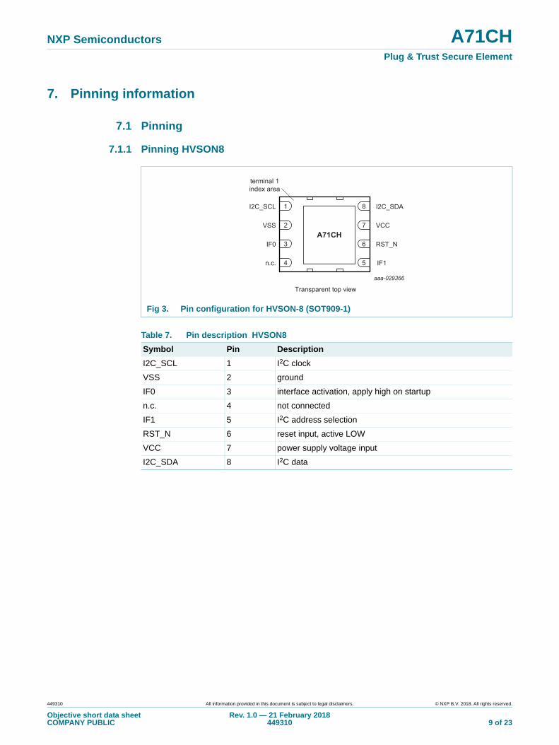
7. Pinning information
7.1 Pinning
7.1.1 Pinning HVSON8
Fig 3. Pin configuration for HVSON-8 (SOT909-1)
Table 7. Pin description HVSON8
Symbol Pin Description
I2C_SCL 1 I2C clock
VSS 2 ground
IF0 3 interface activation, apply high on startup
n.c. 4 not connected
IF1 5 I2C address selection
RST_N 6 reset input, active LOW
VCC 7 power supply voltage input
I2C_SDA 8 I2C data
A71CH
IF1
RST_N
aaa-029366
VCC
I2C_SDA
n.c.
IF0
VSS
I2C_SCL
Transparent top view
4
3
2
1
5
6
7
8
terminal 1index area
449310 All information provided in this document is subject to legal disclaimers. © NXP B.V. 2018. All rights reserved.
Objective short data sheet COMPANY PUBLIC
Rev. 1.0 — 21 February 2018449310 9 of 23

NXP Semiconductors A71CHPlug & Trust Secure Element
8. Package outline
Fig 4. Package outline SOT909-1
449310 All information provided in this document is subject to legal disclaimers. © NXP B.V. 2018. All rights reserved.
Objective short data sheet COMPANY PUBLIC
Rev. 1.0 — 21 February 2018449310 10 of 23
NXP Semiconductors A71CHPlug & Trust Secure Element
9. Packing information
9.1 Reel packing
The A71CH product is available on 7” tape on reel and 13” tape on reel. Details are provided in Table 8.
[1] For details about packing method, product orientation, tape dimensions and labeling for A71 parts in HVSON8 package having an ordering code (12NC) ending 118 refer to Ref. 2.
10. Electrical and timing characteristics
The electrical interface characteristics of static (DC) and dynamic (AC) parameters for pads and functions used for I2C are in accordance with the NXP I2C specification (see Ref. 1).
11. Limiting values
[1] MIL Standard 883-D method 3015; human body model; C = 100 pF, R = 1.5 kΩ; Tamb = −25 °C to +85 °C.
[2] Depending on appropriate thermal resistance of the package.
[3] JESD22-C101, JEDEC Standard Field induced charge device model test method.
Table 8. Reel packing options
Package type Reel type Minimum packing quantity
HVSON8 7” tape on reel 1500
HVSON8 13” tape on reel[1] 6000
Table 9. Limiting values In accordance with the Absolute Maximum Rating System (IEC 60134). Voltages are referenced to VSS (ground = 0 V).
Symbol Parameter Conditions Min Max Unit
VDD supply voltage -0.3 +4.6 V
VI input voltage any signal pad -0.3 +4.6 V
II input current pad I2C_SDA, I2C_SCL
- 10 mA
IO output current pad I2C_SDA, I2C_SCL
- 10 mA
Ilu latch-up current VI < 0 V or VI > VDD - 100 mA
Vesd_hbm electrostatic discharge voltage (Human Body Model)
pads VCC, VSS, RST_N, I2C_SDA, I2C_SCL
[1] ± 2.0 kV
Vesd_cdm electrostatic discharge voltage (Charge Device Model)
pads VCC, VSS, RST_N, I2C_SDA, I2C_SCL
[3] ± 500 V
Ptot Total power dissipation [2] - 1 W
Tstg Storage temperature -55 +125 °C
449310 All information provided in this document is subject to legal disclaimers. © NXP B.V. 2018. All rights reserved.
Objective short data sheet COMPANY PUBLIC
Rev. 1.0 — 21 February 2018449310 11 of 23

NXP Semiconductors A71CHPlug & Trust Secure Element
12. Recommended operating conditions
The A71CH offers two operation modes, the so-called 1V8 mode and the 3V3 mode targeted for battery supplied applications.
Table 10. Recommended operating conditions
Symbol Parameter Conditions Min Typ Max Unit
VDD supply voltage range 3V3 mode range CPU in free runing mode
2.50 3.3 3.6 V
1V8 mode 1.62 1.8 1.98 V
VI DC input voltage on digital I/O pads I2C_SCL, I2C_SDA
3V3 mode 0 3.6 V
1V8 mode 0 3.6 V
VI DC input voltage on digital input pad RST_N
3V3 mode 0 3.6 V
1V8 mode 0 3.6 V
Tamb Operating ambient temperature
A7101 -25 +90 °CA7102 -40 +90 °C
Fig 5. Recommended operating conditions over voltage range
aaa-029326operating conditions
1.62 V 1.98 V 2.5 V 3.6 V
449310 All information provided in this document is subject to legal disclaimers. © NXP B.V. 2018. All rights reserved.
Objective short data sheet COMPANY PUBLIC
Rev. 1.0 — 21 February 2018449310 12 of 23

NXP Semiconductors A71CHPlug & Trust Secure Element
13. Characteristics
13.1 DC characteristics
Measurement conventions
Testing measurements are performed at the contact pads of the device under test. All voltages are defined with respect to the ground contact pad VSS. All currents flowing into the device are considered positive.
13.1.1 General and I2C I/O interface
[1] Maximum value according to Table 10 “Recommended operating conditions”
Table 11. Electrical DC characteristics of I2C_SCL, I2C_SDA and RST_N
Symbol Parameter Conditions Min Typ Max Unit
Input/Output: I2C_SCL, I2C_SDA in push-pull mode
VIH HIGH level input voltage 0.7 VDD VImax[1] V
VIL LOW level input voltage -0.5 0.3 VDD V
IIH HIGH level input current in input mode
VIHmin < VI < VIHmax ± 10 μA
IIL LOW level input current VILmin < VI < VILmax ± 10 μA
VOH HIGH level output voltage IOH = −3.0 mA;
3V3 mode
[2] 0.7 VDD V
IOH = −3.0 mA; 1V8 mode
[2] 0.7 VDD V
VOL LOW level output voltage IOL = 3.0 mA
3V3 mode
0.4 V
IOL = 2.0 mA
1V8 mode
0.2 VDD V
Input/Output: I2C_SCL, I2C_SDA in open-drain mode
VIH HIGH level input voltage 0.7 VDD VImax[1] V
VIL LOW level input voltage -0.5 0.3 VDD V
IIH HIGH level input current in input mode
VIHmin < VI < VIHmax ± 10 μA
IIL LOW level input current VILmin < VI < VILmax ± 10 μA
VOL LOW level output voltage IOL = 3.0 mA
3V3 mode
0.4 V
IOL = 2.0 mA
1V8 mode
0.2 VDD V
Input: RST_N
VIH1 HIGH level input voltage 0.7 VDD VImax[1] V
VIL1 LOW level input voltage -0.3 0.3 VDD V
IIH1 HIGH level RST_N input current VIH1min ≤ VI ≤ VDD[3] ± 20 μA
IIL1 LOW level RST_N input current 0 V ≤ VI ≤ VIL1max; [3] ± 20 μA
449310 All information provided in this document is subject to legal disclaimers. © NXP B.V. 2018. All rights reserved.
Objective short data sheet COMPANY PUBLIC
Rev. 1.0 — 21 February 2018449310 13 of 23
NXP Semiconductors A71CHPlug & Trust Secure Element
[2] : External pull-up resistor 20 kΩ to VDD. The worst case test condition for parameter VOH is present at minimum VDD. For class A supply voltage conditions VDD = 4.5 V is the worst case with respect to the fix specification limit VOHmin = 3.8 V (0.844 VDD). The supply voltage related limit “0.7 VDD“is a stricter requirement than the fix value 3.8 V at high VDD (0.7 VDD = 3.85 V at VDD = 5.5 V). So, in the VDD range 4.5 V to 5.5 V, VOHmin is specified as “the larger value of 0.7 VDD and 3.8 V, respectively”.
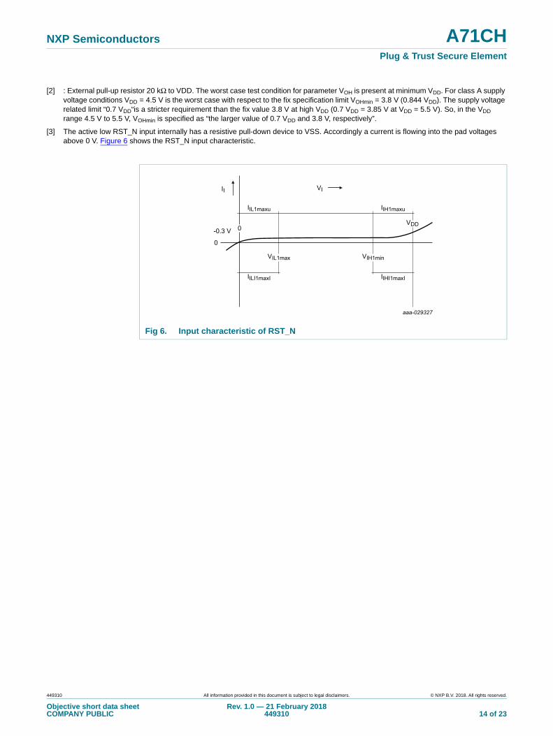
[3] The active low RST_N input internally has a resistive pull-down device to VSS. Accordingly a current is flowing into the pad voltages above 0 V. Figure 6 shows the RST_N input characteristic.
Fig 6. Input characteristic of RST_N
aaa-029327
0
0
-0.3 V
II VI
VIH1minVIL1max
IIL1maxu IIH1maxu
IILI1maxI IIHI1maxI
VDD
449310 All information provided in this document is subject to legal disclaimers. © NXP B.V. 2018. All rights reserved.
Objective short data sheet COMPANY PUBLIC
Rev. 1.0 — 21 February 2018449310 14 of 23
NXP Semiconductors A71CHPlug & Trust Secure Element
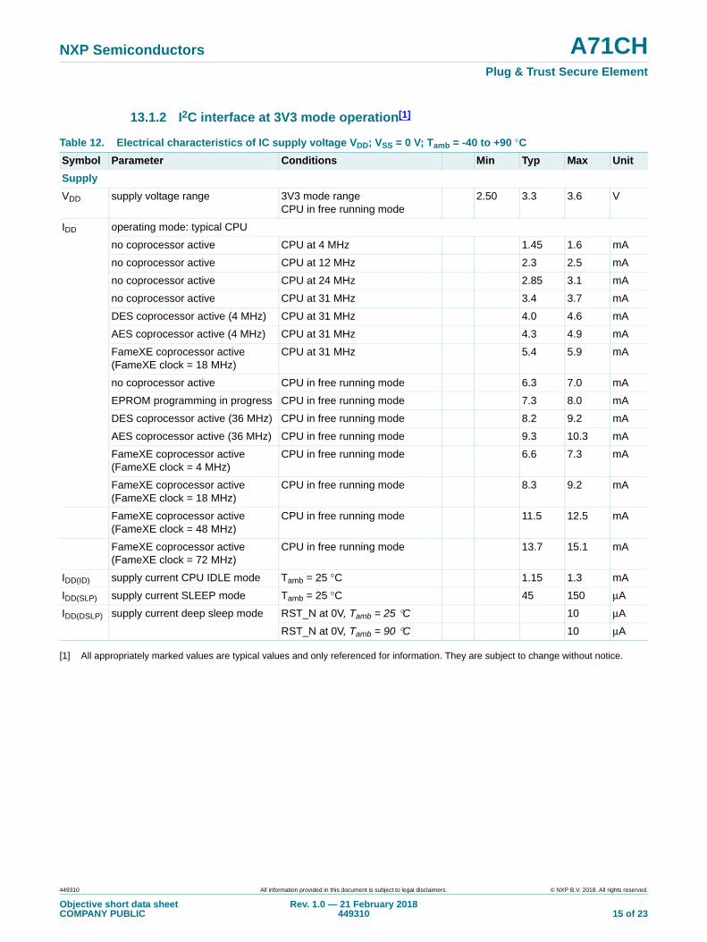
13.1.2 I2C interface at 3V3 mode operation[1]
[1] All appropriately marked values are typical values and only referenced for information. They are subject to change without notice.
Table 12. Electrical characteristics of IC supply voltage VDD; VSS = 0 V; Tamb = -40 to +90 °C
Symbol Parameter Conditions Min Typ Max Unit
Supply
VDD supply voltage range 3V3 mode range CPU in free running mode
2.50 3.3 3.6 V
IDD operating mode: typical CPU
no coprocessor active CPU at 4 MHz 1.45 1.6 mA
no coprocessor active CPU at 12 MHz 2.3 2.5 mA
no coprocessor active CPU at 24 MHz 2.85 3.1 mA
no coprocessor active CPU at 31 MHz 3.4 3.7 mA
DES coprocessor active (4 MHz) CPU at 31 MHz 4.0 4.6 mA
AES coprocessor active (4 MHz) CPU at 31 MHz 4.3 4.9 mA
FameXE coprocessor active (FameXE clock = 18 MHz)
CPU at 31 MHz 5.4 5.9 mA
no coprocessor active CPU in free running mode 6.3 7.0 mA
EPROM programming in progress CPU in free running mode 7.3 8.0 mA
DES coprocessor active (36 MHz) CPU in free running mode 8.2 9.2 mA
AES coprocessor active (36 MHz) CPU in free running mode 9.3 10.3 mA
FameXE coprocessor active (FameXE clock = 4 MHz)
CPU in free running mode 6.6 7.3 mA
FameXE coprocessor active (FameXE clock = 18 MHz)
CPU in free running mode 8.3 9.2 mA
FameXE coprocessor active (FameXE clock = 48 MHz)
CPU in free running mode 11.5 12.5 mA
FameXE coprocessor active (FameXE clock = 72 MHz)
CPU in free running mode 13.7 15.1 mA
IDD(ID) supply current CPU IDLE mode Tamb = 25 °C 1.15 1.3 mA
IDD(SLP) supply current SLEEP mode Tamb = 25 °C 45 150 μA
IDD(DSLP) supply current deep sleep mode RST_N at 0V, Tamb = 25 °C 10 μA
RST_N at 0V, Tamb = 90 °C 10 μA
449310 All information provided in this document is subject to legal disclaimers. © NXP B.V. 2018. All rights reserved.
Objective short data sheet COMPANY PUBLIC
Rev. 1.0 — 21 February 2018449310 15 of 23
NXP Semiconductors A71CHPlug & Trust Secure Element
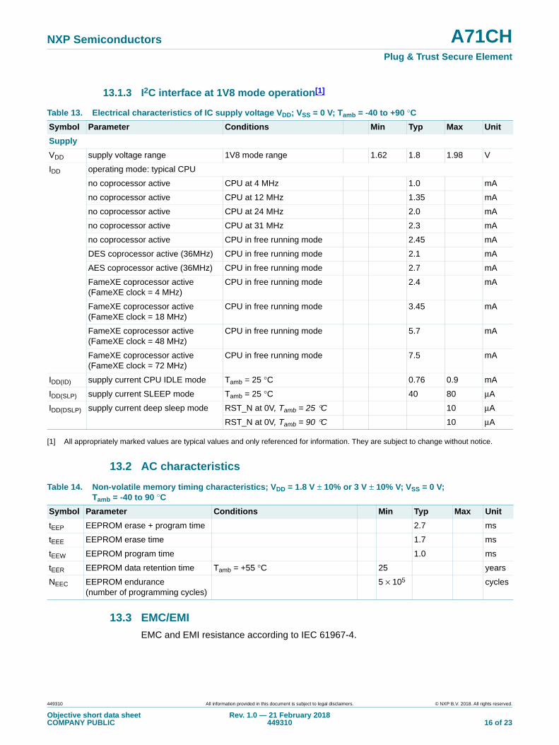
13.1.3 I2C interface at 1V8 mode operation[1]
[1] All appropriately marked values are typical values and only referenced for information. They are subject to change without notice.
13.2 AC characteristics
13.3 EMC/EMI
EMC and EMI resistance according to IEC 61967-4.
Table 13. Electrical characteristics of IC supply voltage VDD; VSS = 0 V; Tamb = -40 to +90 °C
Symbol Parameter Conditions Min Typ Max Unit
Supply
VDD supply voltage range 1V8 mode range 1.62 1.8 1.98 V
IDD operating mode: typical CPU
no coprocessor active CPU at 4 MHz 1.0 mA
no coprocessor active CPU at 12 MHz 1.35 mA
no coprocessor active CPU at 24 MHz 2.0 mA
no coprocessor active CPU at 31 MHz 2.3 mA
no coprocessor active CPU in free running mode 2.45 mA
DES coprocessor active (36MHz) CPU in free running mode 2.1 mA
AES coprocessor active (36MHz) CPU in free running mode 2.7 mA
FameXE coprocessor active (FameXE clock = 4 MHz)
CPU in free running mode 2.4 mA
FameXE coprocessor active (FameXE clock = 18 MHz)
CPU in free running mode 3.45 mA
FameXE coprocessor active (FameXE clock = 48 MHz)
CPU in free running mode 5.7 mA
FameXE coprocessor active (FameXE clock = 72 MHz)
CPU in free running mode 7.5 mA
IDD(ID) supply current CPU IDLE mode Tamb = 25 °C 0.76 0.9 mA
IDD(SLP) supply current SLEEP mode Tamb = 25 °C 40 80 μA
IDD(DSLP) supply current deep sleep mode RST_N at 0V, Tamb = 25 °C 10 μA
RST_N at 0V, Tamb = 90 °C 10 μA
Table 14. Non-volatile memory timing characteristics; VDD = 1.8 V ± 10% or 3 V ± 10% V; VSS = 0 V; Tamb = -40 to 90 °C
Symbol Parameter Conditions Min Typ Max Unit
tEEP EEPROM erase + program time 2.7 ms
tEEE EEPROM erase time 1.7 ms
tEEW EEPROM program time 1.0 ms
tEER EEPROM data retention time Tamb = +55 °C 25 years
NEEC EEPROM endurance (number of programming cycles)
5 × 10⁵ cycles
449310 All information provided in this document is subject to legal disclaimers. © NXP B.V. 2018. All rights reserved.
Objective short data sheet COMPANY PUBLIC
Rev. 1.0 — 21 February 2018449310 16 of 23
NXP Semiconductors A71CHPlug & Trust Secure Element
14. Abbreviations
Table 15. Abbreviations
Acronym Description
AES Advanced Encryption Standard
CRC Cyclic Redundancy Check
DES Digital Encryption Standard
DPA Differential Power Analysis
DSS Digital Signature Standard
ECC Elliptic Curve Cryptography
EEPROM Electrically Erasable Programmable Read-Only Memory
I/O Input/Output
MAC Message Authentication Code
OS Operating System
PKI Public Key Infrastructure
SFI Single Fault Injection
SHA Secure Hash Algorithm
449310 All information provided in this document is subject to legal disclaimers. © NXP B.V. 2018. All rights reserved.
Objective short data sheet COMPANY PUBLIC
Rev. 1.0 — 21 February 2018449310 17 of 23

NXP Semiconductors A71CHPlug & Trust Secure Element
15. References
[1] I2C-bus specification and user manual, Rev. 3.0 — June-19-2007, NXP Semiconductors
[2] SOT909-1; HVSON8; Reel pack; Ordering code (12NC) ending 118; Packing Information; Rev. 2 — 19 April 2013
[3] Application note SCIIC Protocol Specification, Application note, Rev 1.5, an195015 — 31 January 2017
[4] Datasheet A710x family with JCOP 2.4.2. R1 – Secure authentication microcontroller, Rev 3.5, ds236635 — 17 November 2017
449310 All information provided in this document is subject to legal disclaimers. © NXP B.V. 2018. All rights reserved.
Objective short data sheet COMPANY PUBLIC
Rev. 1.0 — 21 February 2018449310 18 of 23
NXP Semiconductors A71CHPlug & Trust Secure Element
16. Revision history
Table 16. Revision history
Document ID Release date Data sheet status Change notice Supersedes
449310 20180221 Objective short data sheet
Modifications: • Initial version
449310 All information provided in this document is subject to legal disclaimers. © NXP B.V. 2018. All rights reserved.
Objective short data sheet COMPANY PUBLIC
Rev. 1.0 — 21 February 2018449310 19 of 23

NXP Semiconductors A71CHPlug & Trust Secure Element
17. Legal information
17.1 Data sheet status
[1] Please consult the most recently issued document before initiating or completing a design.
[2] The term ‘short data sheet’ is explained in section “Definitions”.
[3] The product status of device(s) described in this document may have changed since this document was published and may differ in case of multiple devices. The latest product status information is available on the Internet at URL http://www.nxp.com.
17.2 Definitions
Draft — The document is a draft version only. The content is still under internal review and subject to formal approval, which may result in modifications or additions. NXP Semiconductors does not give any representations or warranties as to the accuracy or completeness of information included herein and shall have no liability for the consequences of use of such information.
Short data sheet — A short data sheet is an extract from a full data sheet with the same product type number(s) and title. A short data sheet is intended for quick reference only and should not be relied upon to contain detailed and full information. For detailed and full information see the relevant full data sheet, which is available on request via the local NXP Semiconductors sales office. In case of any inconsistency or conflict with the short data sheet, the full data sheet shall prevail.
Product specification — The information and data provided in a Product data sheet shall define the specification of the product as agreed between NXP Semiconductors and its customer, unless NXP Semiconductors and customer have explicitly agreed otherwise in writing. In no event however, shall an agreement be valid in which the NXP Semiconductors product is deemed to offer functions and qualities beyond those described in the Product data sheet.
17.3 Disclaimers
Limited warranty and liability — Information in this document is believed to be accurate and reliable. However, NXP Semiconductors does not give any representations or warranties, expressed or implied, as to the accuracy or completeness of such information and shall have no liability for the consequences of use of such information. NXP Semiconductors takes no responsibility for the content in this document if provided by an information source outside of NXP Semiconductors.
In no event shall NXP Semiconductors be liable for any indirect, incidental, punitive, special or consequential damages (including - without limitation - lost profits, lost savings, business interruption, costs related to the removal or replacement of any products or rework charges) whether or not such damages are based on tort (including negligence), warranty, breach of contract or any other legal theory.
Notwithstanding any damages that customer might incur for any reason whatsoever, NXP Semiconductors’ aggregate and cumulative liability towards customer for the products described herein shall be limited in accordance with the Terms and conditions of commercial sale of NXP Semiconductors.
Right to make changes — NXP Semiconductors reserves the right to make changes to information published in this document, including without limitation specifications and product descriptions, at any time and without notice. This document supersedes and replaces all information supplied prior to the publication hereof.
Suitability for use — NXP Semiconductors products are not designed, authorized or warranted to be suitable for use in life support, life-critical or safety-critical systems or equipment, nor in applications where failure or malfunction of an NXP Semiconductors product can reasonably be expected to result in personal injury, death or severe property or environmental damage. NXP Semiconductors and its suppliers accept no liability for inclusion and/or use of NXP Semiconductors products in such equipment or applications and therefore such inclusion and/or use is at the customer’s own risk.
Applications — Applications that are described herein for any of these products are for illustrative purposes only. NXP Semiconductors makes no representation or warranty that such applications will be suitable for the specified use without further testing or modification.
Customers are responsible for the design and operation of their applications and products using NXP Semiconductors products, and NXP Semiconductors accepts no liability for any assistance with applications or customer product design. It is customer’s sole responsibility to determine whether the NXP Semiconductors product is suitable and fit for the customer’s applications and products planned, as well as for the planned application and use of customer’s third party customer(s). Customers should provide appropriate design and operating safeguards to minimize the risks associated with their applications and products.
NXP Semiconductors does not accept any liability related to any default, damage, costs or problem which is based on any weakness or default in the customer’s applications or products, or the application or use by customer’s third party customer(s). Customer is responsible for doing all necessary testing for the customer’s applications and products using NXP Semiconductors products in order to avoid a default of the applications and the products or of the application or use by customer’s third party customer(s). NXP does not accept any liability in this respect.
Limiting values — Stress above one or more limiting values (as defined in the Absolute Maximum Ratings System of IEC 60134) will cause permanent damage to the device. Limiting values are stress ratings only and (proper) operation of the device at these or any other conditions above those given in the Recommended operating conditions section (if present) or the Characteristics sections of this document is not warranted. Constant or repeated exposure to limiting values will permanently and irreversibly affect the quality and reliability of the device.
Terms and conditions of commercial sale — NXP Semiconductors products are sold subject to the general terms and conditions of commercial sale, as published at http://www.nxp.com/profile/terms, unless otherwise agreed in a valid written individual agreement. In case an individual agreement is concluded only the terms and conditions of the respective agreement shall apply. NXP Semiconductors hereby expressly objects to applying the customer’s general terms and conditions with regard to the purchase of NXP Semiconductors products by customer.
No offer to sell or license — Nothing in this document may be interpreted or construed as an offer to sell products that is open for acceptance or the grant, conveyance or implication of any license under any copyrights, patents or other industrial or intellectual property rights.
Document status[1][2] Product status[3] Definition
Objective [short] data sheet Development This document contains data from the objective specification for product development.
Preliminary [short] data sheet Qualification This document contains data from the preliminary specification.
Product [short] data sheet Production This document contains the product specification.
449310 All information provided in this document is subject to legal disclaimers. © NXP B.V. 2018. All rights reserved.
Objective short data sheet COMPANY PUBLIC
Rev. 1.0 — 21 February 2018449310 20 of 23
NXP Semiconductors A71CHPlug & Trust Secure Element
Export control — This document as well as the item(s) described herein may be subject to export control regulations. Export might require a prior authorization from competent authorities.
Quick reference data — The Quick reference data is an extract of the product data given in the Limiting values and Characteristics sections of this document, and as such is not complete, exhaustive or legally binding.
Non-automotive qualified products — Unless this data sheet expressly states that this specific NXP Semiconductors product is automotive qualified, the product is not suitable for automotive use. It is neither qualified nor tested in accordance with automotive testing or application requirements. NXP Semiconductors accepts no liability for inclusion and/or use of non-automotive qualified products in automotive equipment or applications.
In the event that customer uses the product for design-in and use in automotive applications to automotive specifications and standards, customer (a) shall use the product without NXP Semiconductors’ warranty of the product for such automotive applications, use and specifications, and (b) whenever customer uses the product for automotive applications beyond NXP Semiconductors’ specifications such use shall be solely at customer’s own risk, and (c) customer fully indemnifies NXP Semiconductors for any liability, damages or failed product claims resulting from customer design and use of the product for automotive applications beyond NXP Semiconductors’ standard warranty and NXP Semiconductors’ product specifications.
Translations — A non-English (translated) version of a document is for reference only. The English version shall prevail in case of any discrepancy between the translated and English versions.
17.4 Licenses
17.5 TrademarksNotice: All referenced brands, product names, service names and trademarks are the property of their respective owners.
FabKey — is a trademark of NXP B.V.
I2C-bus — logo is a trademark of NXP B.V.
18. Contact information
For more information, please visit: http://www.nxp.com
For sales office addresses, please send an email to: [email protected]
ICs with DPA Countermeasures functionality
NXP ICs containing functionality implementing countermeasures to Differential Power Analysis and Simple Power Analysis are produced and sold under applicable license from Cryptography Research, Inc.
449310 All information provided in this document is subject to legal disclaimers. © NXP B.V. 2018. All rights reserved.
Objective short data sheet COMPANY PUBLIC
Rev. 1.0 — 21 February 2018449310 21 of 23
NXP Semiconductors A71CHPlug & Trust Secure Element
19. Tables
Table 1. A71CH commercial name format . . . . . . . . . . . .2Table 2. Ordering information. . . . . . . . . . . . . . . . . . . . . .6Table 3. A71CH type table . . . . . . . . . . . . . . . . . . . . . . . .6Table 4. A71CH type table . . . . . . . . . . . . . . . . . . . . . . . .6Table 5. A71CH feature table . . . . . . . . . . . . . . . . . . . . . .6Table 6. Pin description WLCSP . . . . . . . . . . . . . . . . . . .8Table 7. Pin description HVSON8 . . . . . . . . . . . . . . . . . .9Table 8. Reel packing options . . . . . . . . . . . . . . . . . . . .12Table 9. Limiting values . . . . . . . . . . . . . . . . . . . . . . . . .12Table 10. Recommended operating conditions . . . . . . . .13Table 11. Electrical DC characteristics of I2C_SCL,
I2C_SDA and RST_N . . . . . . . . . . . . . . . . . . .14Table 12. Electrical characteristics of IC supply voltage VDD;
VSS = 0 V; Tamb = -40 to +90 °C . . . . . . . . . . . . 15Table 13. Electrical characteristics of IC supply voltage VDD;
VSS = 0 V; Tamb = -40 to +90 °C . . . . . . . . . . . 16Table 14. Electrical characteristics of IC supply voltage VDD;
VSS = 0 V; Tamb = -40 to +90 °C . . . . . . . . . . . 17Table 15. Non-volatile memory timing characteristics;
VDD = 1.8 V ± 10% or 3 V ± 10% V; VSS = 0 V; Tamb = -40 to 90 °C. . . . . . . . . . . . . . . . . . . . . . 17
Table 16. I2C timing exceptions for master mode and SCL frequency >200kHz . . . . . . . . . . . . . . . . . . . . . 18
Table 17. Abbreviations . . . . . . . . . . . . . . . . . . . . . . . . . 19Table 18. Revision history . . . . . . . . . . . . . . . . . . . . . . . . 21
20. Figures
Fig 1. A71CH block diagram . . . . . . . . . . . . . . . . . . . . . .1Fig 2. A71CH functional diagram - example Open SSL. .7Fig 3. Pin configuration for WLCSP12 . . . . . . . . . . . . . . .8Fig 4. Ball mapping for WLCSP12 . . . . . . . . . . . . . . . . . .8Fig 5. Pin configuration for HVSON-8 (SOT909-1) . . . . .8
Fig 6. Package outline WLCSP12. . . . . . . . . . . . . . . . . 10Fig 7. Package outline SOT909-1 . . . . . . . . . . . . . . . . . 11Fig 8. Recommended operating conditions over voltage
range . . . . . . . . . . . . . . . . . . . . . . . . . . . . . . . . . . 13Fig 9. Input characteristic of RST_N . . . . . . . . . . . . . . . 15
21. Contents
1 Introduction . . . . . . . . . . . . . . . . . . . . . . . . . . . . 1
2 General description . . . . . . . . . . . . . . . . . . . . . . 22.1 Overview. . . . . . . . . . . . . . . . . . . . . . . . . . . . . . 22.2 A71CH naming conventions . . . . . . . . . . . . . . . 22.3 I2C interface . . . . . . . . . . . . . . . . . . . . . . . . . . . 2
3 Features and benefits . . . . . . . . . . . . . . . . . . . . 33.1 Features . . . . . . . . . . . . . . . . . . . . . . . . . . . . . . 33.2 Security features. . . . . . . . . . . . . . . . . . . . . . . . 33.3 Cryptography features . . . . . . . . . . . . . . . . . . . 4
4 Applications . . . . . . . . . . . . . . . . . . . . . . . . . . . . 54.1 Use Cases and target applications . . . . . . . . . . 5
5 Ordering information. . . . . . . . . . . . . . . . . . . . . 65.1 Ordering options . . . . . . . . . . . . . . . . . . . . . . . . 65.1.1 Samples and final products . . . . . . . . . . . . . . . 65.1.2 Ordering A71CH samples. . . . . . . . . . . . . . . . . 6
6 Functional diagram . . . . . . . . . . . . . . . . . . . . . . 7
7 Pinning information. . . . . . . . . . . . . . . . . . . . . . 87.1 Pinning . . . . . . . . . . . . . . . . . . . . . . . . . . . . . . . 87.1.1 Pinning WLCSP . . . . . . . . . . . . . . . . . . . . . . . . 87.1.2 Pinning HVSON8 . . . . . . . . . . . . . . . . . . . . . . . 8
8 Package outline. . . . . . . . . . . . . . . . . . . . . . . . 10
9 Packing information . . . . . . . . . . . . . . . . . . . . 129.1 Reel packing . . . . . . . . . . . . . . . . . . . . . . . . . 12
10 Electrical and timing characteristics. . . . . . . 12
11 Limiting values . . . . . . . . . . . . . . . . . . . . . . . . 12
12 Recommended operating conditions . . . . . . 13
13 Characteristics . . . . . . . . . . . . . . . . . . . . . . . . 1413.1 DC characteristics . . . . . . . . . . . . . . . . . . . . . 1413.1.1 General and I2C I/O interface . . . . . . . . . . . . 1413.1.2 Electrical characteristics . . . . . . . . . . . . . . . . 1513.1.3 I2C interface at 3V3 mode operation[1] . . . . . 1613.1.4 I2C interface at 1V8 mode operation[1] . . . . . 1713.2 AC characteristics . . . . . . . . . . . . . . . . . . . . . 1713.2.1 I2C timing exceptions. . . . . . . . . . . . . . . . . . . 1713.3 EMC/EMI . . . . . . . . . . . . . . . . . . . . . . . . . . . . 18
14 Abbreviations . . . . . . . . . . . . . . . . . . . . . . . . . 19
15 References. . . . . . . . . . . . . . . . . . . . . . . . . . . . 20
16 Revision history . . . . . . . . . . . . . . . . . . . . . . . 21
17 Legal information . . . . . . . . . . . . . . . . . . . . . . 2217.1 Data sheet status . . . . . . . . . . . . . . . . . . . . . . 22
449310 All information provided in this document is subject to legal disclaimers. © NXP B.V. 2018. All rights reserved.
Objective short data sheet COMPANY PUBLIC
Rev. 1.0 — 21 February 2018449310 22 of 23
continued >>
NXP Semiconductors A71CHPlug & Trust Secure Element
17.2 Definitions. . . . . . . . . . . . . . . . . . . . . . . . . . . . 2217.3 Disclaimers . . . . . . . . . . . . . . . . . . . . . . . . . . . 2217.4 Licenses . . . . . . . . . . . . . . . . . . . . . . . . . . . . . 2317.5 Trademarks. . . . . . . . . . . . . . . . . . . . . . . . . . . 23
18 Contact information. . . . . . . . . . . . . . . . . . . . . 23
19 Tables . . . . . . . . . . . . . . . . . . . . . . . . . . . . . . . . 24
20 Figures . . . . . . . . . . . . . . . . . . . . . . . . . . . . . . . 24
21 Contents . . . . . . . . . . . . . . . . . . . . . . . . . . . . . . 24
© NXP B.V. 2018. All rights reserved.
For more information, please visit: http://www.nxp.com For sales office addresses, please send an email to: [email protected]
Date of release: 21 February 2018 449310
Please be aware that important notices concerning this document and the product(s) described herein, have been included in section ‘Legal information’.