spec4.1 three–axis mems sensor with 16-bit adcs and signal conditioning the sh200q consists of...
TRANSCRIPT

SH200Q Preliminary Specification
SENODIA Technologies Co., Ltd. | www.senodia.com Page 1 of 42 Rev 1.0
Features and Benefits VDD range: 2.6V~3.6V Low power consumption: 2.5mA Small size: 3.3mmx3.3mm Operating temperature range:- 40℃to
85℃ High resolution and dynamic range Low zero rate output drift High-performance MEMS sensor in SOI
yielding a superior long-term behavior reliability and dynamic range
Cost effective and Compact Solution On chip EPROM trimming On-chip 16 bits ADC SPI &I2C interface
Applications Activity monitoring, step-counting Navigation Vibration measurement, also for active
damping Six-dimensional tracking of trajectories EIS & OIS camera applications Motion-enabled game and application
framework Location based services, points of
interest, and dead reckoning Handset and portable gaming Motion-based game controllers Toys
General Description The SH200Q is a very small, 6 axis inertial sensor, consisting of: A digital, triaxial 16bit acceleration sensor and a digital, triaxial 16bit, ±2000°/s gyroscope. The SH200Q allows very low-noise measurement of angular rates and accelerations in 3 perpendicular axis and thus senses tilt, motion, shock and vibration in mobile phones, handhelds, computer peripherals, man-machine interfaces, remote and game controllers. A single QFN package contains a high performance silicon micro machined sensor with signal conditioning circuitry. It provides excellent temperature stability and high resolution over the operating temperature range (-40℃~ 85℃) It has applications-programmable full-scale-range of +-125º/s, ±250 º/s, ±500º/s, ±1000º/s and ±2000º/s. SH200Q is capable of detecting rates with -3dB bandwidth up to 200Hz. The SH200Q delivers output signal proportional to angular rate. SH200Q includes low-pass filters and EPROM for on-chip factory calibration for the sensor. The SH200Q is provided in Quad Flat No-lead (QFN) package.
Order Information
Model Name Full Scale Range Package Description
SH200Q ±2000 º/s / ±16g 24-pin QFN, 3.3x 3.3 x 0.9mm3

SH200Q Preliminary Specification
SENODIA Technologies Co., Ltd. | www.senodia.com Page 2 of 42 Rev 1.0
Contents
1. Functional Diagram............................................................................................................. 5
2. SH200Q Specifications ...................................................................................................... 6
2.1 Gyroscope sensor specifications ..................................................................................... 6
2.2 Accelerometer sensor specifications .............................................................................. 7
2.3 Electrical characteristics ................................................................................................... 7
2.4 Digital interface characteristics ........................................................................................ 8
2.4.1 SPI-serial peripheral interface................................................................................... 8
2.4.2 I2C- Inter-IC control interface .................................................................................... 8 2.5 Absolute maximum ratings ............................................................................................... 9
3. Pin Description ..................................................................................................................... 10
3.1 24-pin QFN ....................................................................................................................... 10
4. Functional Explanation ........................................................................................................ 11
4.1 Three–Axis MEMS sensor with 16-bit ADCs and signal conditioning ..................... 11
4.2 Auxiliary IIC serial interface ............................................................................................ 11
4.3 FIFO ................................................................................................................................... 12
4.4 Interrupt ............................................................................................................................. 12
4.4.1 General features ....................................................................................................... 12
4.4.2 New data interrupt .................................................................................................... 13
4.4.3 Activity detection interrupt ........................................................................................ 13
4.4.4 Inactivity detection interrupt .................................................................................... 14
4.4.5 Free-fall detection interrupt ..................................................................................... 15
5. Digital Interface ..................................................................................................................... 15
5.1 Interfaces .......................................................................................................................... 15
5.2 Primary interface .............................................................................................................. 16
5.2.1 Primary interface I2C/SPI protocol selection ........................................................ 16
5.2.2 Primary SPI interface ............................................................................................... 16
5.2.3 Primary I2C interface ................................................................................................ 17
6. Register Map and Description ............................................................................................ 19
6.1 Accelerometer X-Axis data low byte ............................................................................. 19
6.2 Accelerometer X-Axis data high byte ........................................................................... 19
6.3 Accelerometer Y-Axis data low byte ............................................................................. 20
6.4 Accelerometer Y-Axis data high byte ........................................................................... 20
6.5 Accelerometer Z-Axis data low byte ............................................................................. 21
6.6 Accelerometer Z-Axis data high byte ............................................................................ 21
6.7 Gyroscope X-Axis data low byte ................................................................................... 21
SH200Q Preliminary Specification
SENODIA Technologies Co., Ltd. | www.senodia.com Page 3 of 42 Rev 1.0
6.8 Gyroscope X-Axis data high byte .................................................................................. 22
6.9 Gyroscope Y-Axis data low byte ................................................................................... 22
6.10 Gyroscope Y-Axis data high byte ................................................................................ 23
6.11 Gyroscope Z-Axis data low byte ................................................................................. 23
6.12 Gyroscope Z-Axis data high byte ................................................................................ 23
6.13 Temperature data low byte .......................................................................................... 24
6.14 Temperature data high byte ......................................................................................... 24
6.15 Accelerometer configuration ........................................................................................ 25
6.16 Gyroscope configuration .............................................................................................. 25
6.17 GYRO configuration 1 ................................................................................................... 26
6.18 FIFO configuration ......................................................................................................... 27
6.19 Interrupt configuration ................................................................................................... 27
6.20 Interrupt enable .............................................................................................................. 28
6.21 Accelerometer data format ........................................................................................... 28
6.22 ACT thresh...................................................................................................................... 29
6.23 InACT thresh .................................................................................................................. 29
6.24 ACT time thresh ............................................................................................................. 30
6.25 InACT time thresh .......................................................................................................... 30
6.26 ACT-InACT configuration ............................................................................................. 31
6.27 Free-Fall threshold ........................................................................................................ 31
6.28 Free-Fall Time Threshold ............................................................................................. 32
6.29 Interrupt count limit ........................................................................................................ 32
6.30 Gyroscope full scale range........................................................................................... 32
6.31 Interrupt status ............................................................................................................... 33
6.32 Act-InACT status ............................................................................................................ 34
6.33 accelerometer FIFO Status .......................................................................................... 34
6.34 Gyroscope FIFO Status ................................................................................................ 34
6.35 chip ID ............................................................................................................................. 35
7 Application Information ......................................................................................................... 35
7.1 Orientation of Axes .......................................................................................................... 35
7.2 Typical Application Circuit .............................................................................................. 36
7.3 Package Outline Dimensions ......................................................................................... 37
7.3.1 QFN Package Outline Dimensions ........................................................................ 37 7.4 Package laser Mark ......................................................................................................... 38
7.5 Packing of the Chips ....................................................................................................... 39

SH200Q Preliminary Specification
SENODIA Technologies Co., Ltd. | www.senodia.com Page 4 of 42 Rev 1.0
7.5.1 Packing direction ....................................................................................................... 39 7.6 Labels ................................................................................................................................ 39
7.7 Packing .............................................................................................................................. 39
7.8 Solder Reflow Curve ....................................................................................................... 40
7.8.1 Solder Reflow curve ................................................................................................. 40 7.9 Storage condition ............................................................................................................. 41
8. Reliability ............................................................................................................................... 41
8.1 Reliability standard: ......................................................................................................... 41
9. Environment Compliant ....................................................................................................... 42
10 Revision History .................................................................................................................. 42
11. Disclaimer ........................................................................................................................... 42
SH200Q Preliminary Specification
SENODIA Technologies Co., Ltd. | www.senodia.com Page 5 of 42 Rev 1.0
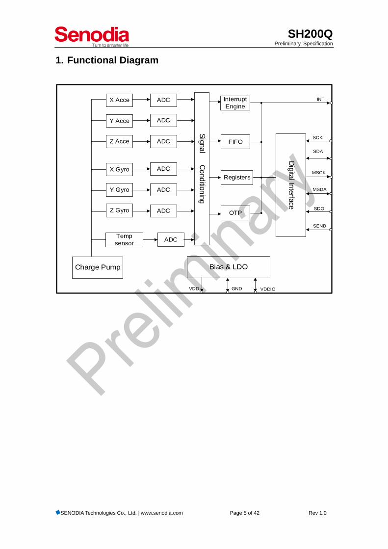
1. Functional Diagram
Charge Pump Bias & LDO
VDD
X Gyro
Y Gyro
ADC
ADCSignal Conditioning
Temp sensor
Digital InterfaceInterrupt Engine
FIFO
Registers
INT
VDDIO
ADC
SCK
SDA
MSCK
MSDA
SDOZ Gyro ADC OTP
X Acce
Y Acce
ADC
ADC
Z Acce ADC
GND
SENB

SH200Q Preliminary Specification
SENODIA Technologies Co., Ltd. | www.senodia.com Page 6 of 42 Rev 1.0
2. SH200Q Specifications All parameters specified are @ VDD=3.0V and T=25℃, unless otherwise noted.
2.1 Gyroscope sensor specifications
Parameter Conditions Min. Typ. Max. Unit
Full Scale Range
±2000 º/s ±1000º/s ±500 º/s ±250 º/s ±125 º/s
º/s
Sensitivity/Scale Factor
16.4 32.8 65.5 131 262
LSB/ º/s
Non-Linearity Best Fit Straight Line
±0.2 % of FS
Gyro_ODR Angular rate output rate
32 250 500
1000 8K 16K 32K
Hz
Scale Factor Drift -40℃~85℃ 0.05 %/℃
Zero Rate Temperature Drift
-40℃~85℃ 0.2 º/s/℃
Bandwidth(-3dB) 200 Hz
Rate output Noise Density
0.019 @ 100Hz
dps/√Hz
Cross-sensitivity ±1 %
Initial ZRO tolerance ±5 º/s

SH200Q Preliminary Specification
SENODIA Technologies Co., Ltd. | www.senodia.com Page 7 of 42 Rev 1.0
2.2 Accelerometer sensor specifications
Parameter Conditions Min. Typ. Max. Unit
Acceleration Range selectable via I2C ±4 ±8 ±16
g
Sensitivity/Scale Factor
8192 4096 2048
LSB/g
Acc_ODR Acceleration rate output data rate
1000 500 250 125 64 32 16 8
Hz
Sensitivity Drift -40℃~85℃ ±0.02 %/℃
Zero-g offset -40℃~85℃ ±80 mg
output rate noise 150 ug/√Hz
Non-Linearity ±0.5 %FS
2.3 Electrical characteristics
Electrical characteristics @ VDD=3.0V, T=25℃ unless otherwise noted Symbol Parameter Condition Min. Typ. Max. Unit
VDD Supply voltage 2.6 3 3.6 V VDDIO 1.62 1.8 3.6 V
Idd Supply current VDD=3.0V 2.5 mA Iddpd Power down
current VDD=3.0V 3.7 uA
VIL Digital Low-level input voltage
0.3*VDDIO V
VIH Digital high-level input voltage
0.7*VDDIO V
VOL Digital low-level output voltage
0.2 V
VOH Digital high-level output voltage
VDDIO– 0.2

SH200Q Preliminary Specification
SENODIA Technologies Co., Ltd. | www.senodia.com Page 8 of 42 Rev 1.0
2.4 Digital interface characteristics
2.4.1 SPI-serial peripheral interface
Subject to general operation conditions like VDD, operating temperature and PCB design.
symbol parameter value
unit Min Max
tsck SPI clock period 125 ns fsck SPI frequency 8 MHz tsucsb CSB setup time 8 ns thcsb CSB hold time 20 ns tsusdi SDI setup time 8 ns thsdi SDI hold time 20 ns tvdsdo SDO valid time 60 ns thsdo SDO hold time 8 ns tdissdo SDO disable time 60 ns
CSB
SCK
SDI
SDO
tsucsb thcsb
tsusdithsdi
tsck
thsdo tdissdotvdsdo
SPI timing diagram
2.4.2 I2C- Inter-IC control interface
Subject to general operation conditions like VDD, operating temperature and PCB design.
symbol parameter value
unit Min Max
fsck I2C frequency 400 KHz tlow I2C clock low time 1.5 us thigh I2C clock high time 0.7 us tsudat SDA data setup time 150 ns thdat SDA data hold time 0 1 us tsursta repeat start condition setup time 0.6 us

SH200Q Preliminary Specification
SENODIA Technologies Co., Ltd. | www.senodia.com Page 9 of 42 Rev 1.0
thsta start condition hold time 0.6 us tsusp stop condition setup time 0.6 us
SDA
SCK
SDA
thsta
tsudat
tsursta tsuspthigh
tlow
thdat trtf
I2C timing diagram
2.5 Absolute maximum ratings
Stress above those listed as “Absolute Maximum Ratings” may cause permanent damage to the device. Exposure to absolute-maximum-rated conditions for extended periods may affect device reliability.
Parameter Rating Operating supply voltage -0.3V ~ 6V Operating Temperature Range -40℃ ~ 85℃ Storage Temperature Range -40℃ ~ 105℃ ESD ( HBM ) 2000V ESD ( MM ) 200V Latch-up JEDEC78E Class I,±200mA

SH200Q Preliminary Specification
SENODIA Technologies Co., Ltd. | www.senodia.com Page 10 of 42 Rev 1.0
3. Pin Description
3.1 24-pin QFN
2
1
3
4
5
6
18
17
16
15
14
13
24 23 22 21 20 19
7 8 9 10 11 12
17
18
16
15
14
13
1
2
3
4
5
6
19 20 21 22 23 24
12 11 10 9 8 7
Top View
Bottom View
SD
A
RE
SV
NC
SC
K
NC
NC
NC
NC
NC
NC
NC
NC
NC
MS
DA
GND
VDD
INT
NC
MC
LK
VD
DIO
SD
OS
EN
B
RE
SV
RE
SV
Pin No. Pin
Name Pin Function
1~6 NC Not internally connected. 7 MCLK Auxiliary IIC serial clock, for connecting to external sensors 8 VDDIO Digital I/O supply voltage 9 SDO IIC slave Address LSB (A0), Serial data output in SPI. 10 RESV Reserved. Do not connect 11 NC Not internally connected. 12 INT Interrupt digital output(totem pole or open-drain) 13 VDD Power supply voltage and Digital supply voltage 14~17 NC Not internally connected. 18 GND Power supply ground 19 RESV Reserved. Do not connect 20 RESV Reserved. Do not connect 21 MSDA Auxiliary IIC serial data, for connecting to external sensors 22 SENB I2C/SPI (CSB)Protocol select: 1: SPI idle mode/I2C
communication enabled; 0: SPI communication mode/I2C disabled
23 SCK IIC serial clock, SPI serial clock 24 SDA IIC serial data, serial data input SDI in SPI

SH200Q Preliminary Specification
SENODIA Technologies Co., Ltd. | www.senodia.com Page 11 of 42 Rev 1.0
4. Functional Explanation Overview The SH200Q is comprised of the several key blocks and functions: Three-axis MEMS angular rate sensor/acceleration sensor with 16-bit ADCs and
signal conditioning Digital signal processor Auxiliary IIC interface FIFO Interrupts Digital-Output Temperature Sensor
4.1 Three–Axis MEMS sensor with 16-bit ADCs and signal conditioning
The SH200Q consists of three independent angular rate sensors and independent acceleration sensors. It detects rotation on the X, Y and Z axes and acceleration on the X, Y and Z axes. When the gyro is rotated around any of these sense axes, the movement caused by Coriolis Effect will be detected. And when the accelerometer is moving along any of these sense axes, the movement caused by acceleration will be detected. The resulting signal is amplified, demodulated, and filtered to produce a voltage that is proportional to the angular rate or the acceleration rate. For each axis an on-chip 16-bit ADC is used to digitize the output voltage. The full-range of the gyroscope part is ±2000º/s and the full-range of the accelerometer part is programmable at ±4/8/16g.
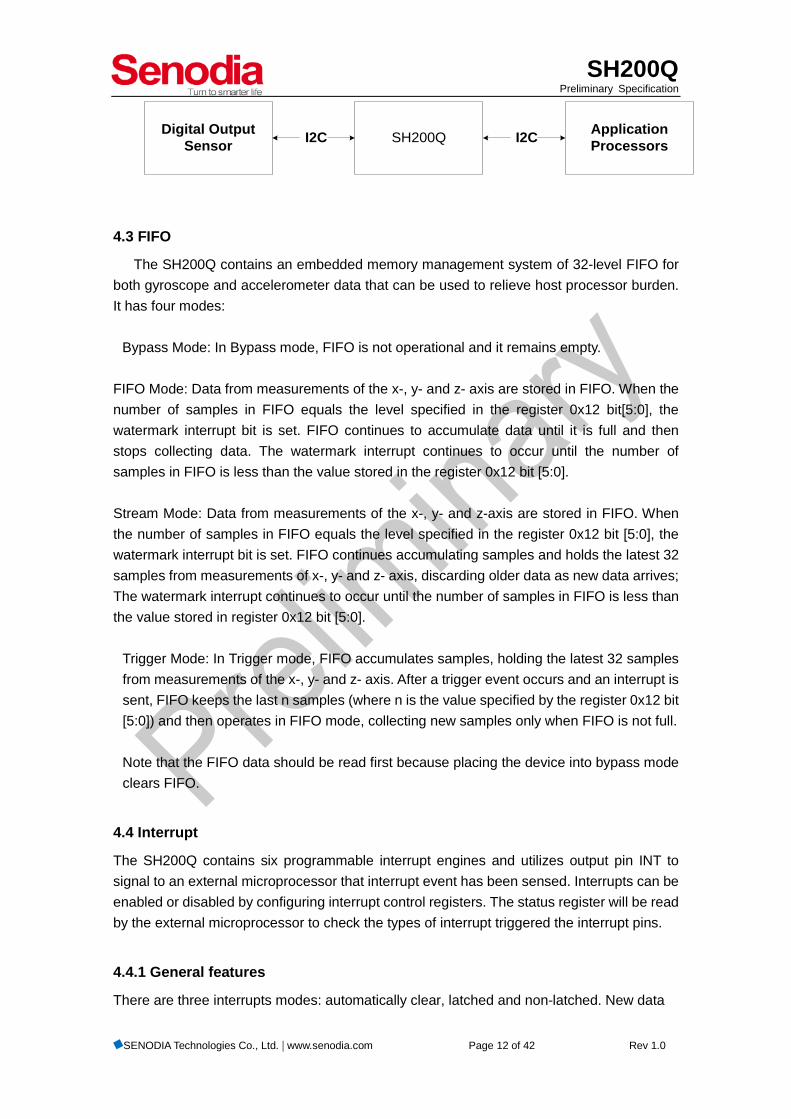
4.2 Auxiliary IIC serial interface
The SH200Q has an auxiliary IIC bus which allows an external system processor to act as master and directly communicate to the external sensors connected to the secondary I2C bus pins (MSDA and MSCK). This is useful for configuring the external sensors, or for keeping the SH200Q in a low-power mode, when only sensors are to be used. In this mode, the secondary I2C bus control logic (third-party sensor Interface block) of the SH200Q is disabled, and the secondary I2C pins MSDA and MSCK are connected to the main I2C bus through analog switches.
The diagram below shows an application processor can communicate to the digital output sensor connected to SH200Q through the Auxiliary IIC bus.
SH200Q Preliminary Specification
SENODIA Technologies Co., Ltd. | www.senodia.com Page 12 of 42 Rev 1.0
SH200QDigital OutputSensor
Application ProcessorsI2C I2C
4.3 FIFO
The SH200Q contains an embedded memory management system of 32-level FIFO for both gyroscope and accelerometer data that can be used to relieve host processor burden. It has four modes:
Bypass Mode: In Bypass mode, FIFO is not operational and it remains empty.
FIFO Mode: Data from measurements of the x-, y- and z- axis are stored in FIFO. When the number of samples in FIFO equals the level specified in the register 0x12 bit[5:0], the watermark interrupt bit is set. FIFO continues to accumulate data until it is full and then stops collecting data. The watermark interrupt continues to occur until the number of samples in FIFO is less than the value stored in the register 0x12 bit [5:0].
Stream Mode: Data from measurements of the x-, y- and z-axis are stored in FIFO. When the number of samples in FIFO equals the level specified in the register 0x12 bit [5:0], the watermark interrupt bit is set. FIFO continues accumulating samples and holds the latest 32 samples from measurements of x-, y- and z- axis, discarding older data as new data arrives; The watermark interrupt continues to occur until the number of samples in FIFO is less than the value stored in register 0x12 bit [5:0].
Trigger Mode: In Trigger mode, FIFO accumulates samples, holding the latest 32 samples from measurements of the x-, y- and z- axis. After a trigger event occurs and an interrupt is sent, FIFO keeps the last n samples (where n is the value specified by the register 0x12 bit [5:0]) and then operates in FIFO mode, collecting new samples only when FIFO is not full. Note that the FIFO data should be read first because placing the device into bypass mode clears FIFO.
4.4 Interrupt
The SH200Q contains six programmable interrupt engines and utilizes output pin INT to signal to an external microprocessor that interrupt event has been sensed. Interrupts can be enabled or disabled by configuring interrupt control registers. The status register will be read by the external microprocessor to check the types of interrupt triggered the interrupt pins.
4.4.1 General features
There are three interrupts modes: automatically clear, latched and non-latched. New data

SH200Q Preliminary Specification
SENODIA Technologies Co., Ltd. | www.senodia.com Page 13 of 42 Rev 1.0
ready interrupt is automatically cleared after a fixed time. Other interrupts can be configured as latched (0x13 bit[6]to ‘0’)or non-latched(0x13 bit[6]to ‘1’) modes. Non-latched interrupts will be cleared after a defined period of time (by setting register 0x1E). For latched interrupts, there are two ways to clear the interrupts: random read clear (0x13 bit [4] to ‘1’) or status read clear (0x13 bit [4] to ‘0’). The interrupt pins can be set as either open-drain output or push-pull output by configuring register 0x13 bits [5]. When setting register 0x13 bit [5] to ‘1’, the output pin is open-drain output; the output pin is push-pull output if set register 0x13 bit [5]to ‘0’. The active level of interrupt pins is determined by register 0x13 bit [7], when register 0x13 bit [7] is ‘1’(‘0’), the active level of interrupt pins is active high(low).
4.4.2 New data interrupt
The new data interrupt is generated after a new set of data stored in the data register. The interrupt is automatically cleared when the next data acquisition cycle starts. It is enabled (disabled) by writing ´1´ (´0´) to register 0x14bit [5]. The interrupt status is stored in register 0x2Cbit [5].
4.4.3 Activity detection interrupt
Activity detection uses consecutive acceleration values to detect changes in motion. Activity detection interrupt is enabled (disabled) by writing ´1´ (´0´) to register 0x14bit [1]. There are two types of operation for activity detection: ac-coupled and dc-coupled operation. By writing ‘1’ (‘0’) to register 0x1Bbit [7], ac-coupled (dc-coupled) operation is selected. In dc-coupled operation, the current acceleration magnitude is compared directly with register 0x17 to determine whether activity is detected. In ac-coupled operation for activity detection, the acceleration value at the start of activity detection is taken as a reference value. New samples of acceleration are then compared to this reference value, and if the magnitude of the difference exceeds the register 0x17 value, then activity is detected. The activity interrupt is generated only after a predefined number of consecutive acceleration values exceed the register 0x17 value. The number is set by the register 0x19. The activity detection threshold is defined by the register 0x17. The meaning of register 0x17 depends on the range setting. 1 LSB of register 0x17 corresponds to 8 mg in 4g-range, 16 mg in 8g-range, and 32 mg in 16g-range. Each axis can be individually selected to participate in detecting activity. The axis participates the activity detection is determined by register 0x1Bbit [6:4]. A setting of 0 excludes the selected axis from participation. If all axes are excluded, the function is disabled. For activity detection, all participating axes are logically OR’ed, causing the activity

SH200Q Preliminary Specification
SENODIA Technologies Co., Ltd. | www.senodia.com Page 14 of 42 Rev 1.0
function to trigger when any of the participating axes exceeds the threshold for register 0x19 consecutive number of samples. The interrupt status is stored in register 0x2Cbit [1]. The activity interrupt supplies additional information about the detected activity. The axis which triggered the interrupt is given by that one of register 0x2D bit [6:4] that contains a value of ´1´. The sign of the triggering slope is held in register 0x2D bit [7] until the interrupt is retriggered. If register 0x2D bit[7] = ´0´ (´1´), the sign is positive (negative). Activity detection cannot be enabled when inactivity detection is enabled.
4.4.4 Inactivity detection interrupt
Inactivity detection uses consecutive acceleration values to detect lack of motion. Inactivity detection interrupt is enabled (disabled) by writing ´1´ (´0´) to register 0x14 bit [0].There are two types of operation for inactivity detection: ac-coupled and dc-coupled operation. By writing ‘1’ (‘0’) to register 0x1B bit[3], ac-coupled (dc-coupled) operation is selected. In dc-coupled operation, the current acceleration magnitude is compared directly with register 0x18 to determine whether inactivity is detected. In ac-coupled operation for inactivity detection, the acceleration value at the start of activity detection is taken as a reference value. New samples of acceleration are then compared to this reference value, and if the magnitude of the difference is less than the register 0x18 value, then inactivity is detected. The inactivity interrupt is generated only after within a predefined period of time, all participating axis’ acceleration values are less than the register 0x18 value. The time is set by the register 0x1A. The time unit is second. The inactivity detection threshold is defined by the register 0x18. The meaning of register 0x18 depends on the range setting. 1 LSB of register 0x18 corresponds to 8 mg in 4g-range, 16 mg in 8g-range, and 32 mg in 16g-range. Each axis can be individually selected to participate in detecting inactivity. The axis participates the inactivity detection is determined by register 0x1B bit [2:0]. A setting of 0 excludes the selected axis from participation. If all axes are excluded, the function is disabled. For inactivity detection, all participating axes are logically AND’ed, causing the inactivity function to trigger when all of the participating axes are less than the threshold for at least a period of time specified in register 0x1A. The interrupt status is stored in register 0x2C bit [0]. The inactivity interrupt supplies additional information about the detected inactivity. The axis which triggered the interrupt is given by register 0x2D bit [6:4] that contains a value of ´1´. The sign of the triggering slope is

SH200Q Preliminary Specification
SENODIA Technologies Co., Ltd. | www.senodia.com Page 15 of 42 Rev 1.0
held in register 0x2D bit [7] until the interrupt is retriggered. If register 0x2D bit [7] = ´0´ (´1´), the sign is positive (negative). Inactivity detection cannot be enabled when activity detection is enabled.
4.4.5 Free-fall detection interrupt
Free-fall detection detects whether the device is falling. If the sum of absolute accelerations of all three axis |acc_x| + |acc_y| + |acc_z| is less than the threshold value set by register 0x1C for longer time than the value is specified in the register 0x1D, free-fall detection interrupt is generated. The free-fall detection interrupt is enabled (disabled) by writing ´1´ (´0´) to register 0x14 bit [2] and the interrupt status is stored in register 0x2C bit [2]. The register 0x1C defines the threshold value. The meaning of register 0x1C depends on the range setting. 1 LSB of register 0x1C corresponds to16 mg in 4g-range, 32 mg in 8g-range, and 64 mg in 16g-range. The sum of absolute acceleration of all axes |acc_x| + |acc_y| + |acc_z| is compared with the value in register 0x1C to determine if a free-fall event occurred. The register 0x1D defines the time value representing the minimum time that the value of all axes must be less than register 0x1C to generate a free-fall interrupt. The scale factor is 2ms/LSB. A value of 0 may result in undesirable behavior if the free-fall interrupt is enabled. Values between 100 ms and 350 ms (0x14 to 0x46) are recommended.
5. Digital Interface
5.1 Interfaces
SH200Q has both primary interface (I2C and SPI configurable) and secondary interface. The secondary interface supports I2C only.
The secondary I2C bus allows an external system processor to act as master and directly communicate to the external device connected to the secondary I2C bus pins (MSDA and MSCK). This is useful for configuring the magnetometer along with SH200Q to build a 9-DoF solution. In this mode, the secondary I2C bus control logic (third-party accelerometer Interface block) of the SH200Q is disabled, and the secondary I2C pins MSDA and MSCK are connected to the main I2C bus through analog switches.
The diagram below shows an application processor can communicate to the digital
output sensor connected to SH200Q through the Auxiliary IIC bus.
SH200QDigital OutputSensor
Application ProcessorsI2C I2C

SH200Q Preliminary Specification
SENODIA Technologies Co., Ltd. | www.senodia.com Page 16 of 42 Rev 1.0
5.2 Primary interface
By default, the SH200Q operates in I2C mode. The SH200Q interface can also be configurable to operate in an SPI 4-wire configuration. I2C and SPI digital interface share partly the same pins.
5.2.1 Primary interface I2C/SPI protocol selection
The protocol is automatically selected based on the chip select CSB pin behavior after power-up. AT power-up, SH200Q is in I2C mode. If CSB is connected to VDDIO during power-up and not changed the SH200Q interface works in I2C mode. The interface switches from I2C to SPI mode when a “high” to “low” transition happens on CSB pin.
5.2.2 Primary SPI interface
The SPI interface of the SH200Q is compatible with two modes, ‘00’ (CPOL =’0’ and CPHA=’0’) and ‘11’ (CPOL =’1’ and CPHA =’1’). The automatic selection between ‘00’ and ‘11’ is controlled based on the value of SCK after a falling edge of CSB. The SH200Q only supports SPI 4-wire mode. The basic write, read and multiple write, read operations are illustrated in below waveforms.
CSB
SCK
SDI
SDO
R/W AD6 AD5 AD4 AD3 AD2 AD1 AD0 DIN7 DIN6 DIN5 DIN4 DIN3 DIN2 DIN1 DIN0
Z
Tri-state
Figure 4-wire SPI write sequence (mode ’11’)

SH200Q Preliminary Specification
SENODIA Technologies Co., Ltd. | www.senodia.com Page 17 of 42 Rev 1.0
CSB
SCK
SDI
SDO
R/W AD6 AD5 AD4 AD3 AD2 AD1 AD0 DIN7 DIN6 DIN5 DIN4 DIN3 DIN2 DIN1 DIN0
4-wire SPI read Sequence
DO7 DO6 DO5 DO4 DO3 DO2 DO1 DO0 Tri-state
Figure 4-wire SPI read sequence (mode ‘11’) The data bits shown in above waveforms are: Bit0: Read/Write bit. When ‘0’, the data SDI is written into the chip. When ‘1’, the data SDO are read out from them chip. Bit1-7: Address AD[6:0]. Bit8-15: When in write mode, these are the data from SDI written into the address AD, when in read mode, these are data read from the address AD. Multiple read and write operations are done by keeping CSB low and continuing the data transaction and only the first address is written, addresses are automatically incremented internally as long as CSB stays active. Multiple read and write are shown in figure below:
CSB
SCK
SDI
SDO
R/W AD6 AD5 AD4 AD3 AD2 AD1 AD0
4-wire SPI Multiple read Sequence
DO7 DO6 DO5 DO4 DO3 DO2 DO1 DO0 Tri-stateDO15 DO14 DO13 DO12 DO11 DO10 DO9 DO8
R/W AD6 AD5 AD4 AD3 AD2 AD1 AD0 DIN7 DIN6 DIN5 DIN4 DIN3 DIN2 DIN1 DIN0
Z
Tri-state
4-wire SPI Multiple write Sequence
DIN15 DIN14 DIN13 DIN12 DIN11 DIN10 DIN9 DIN8
CSB
SCK
SDI
SDO
5.2.3 Primary I2C interface
The SH200Q I2C is a save bus. There are two signals associate with the I2C bus: the serial clock SCL and serial data SDA. The SDA is a bi-directional line used to send and receive

SH200Q Preliminary Specification
SENODIA Technologies Co., Ltd. | www.senodia.com Page 18 of 42 Rev 1.0
data to or from the interface. Both lines must be connected to VDDIO through external pull-up resistors. The default I2C address of SH200Q is 0b1101100. It is used if the SDO pin is pulled to ‘GND’. The alternative address 0b1101101 is selected by pulling the SDO to VDDIO. The I2C bus is implemented with fast mode (400 KHz) and the standard mode. Data transfer with acknowledge is mandatory. The transmitter must release the SDA line during the acknowledge pulse. The receiver then must pull the SDA line ‘low’ so it remains low during the high period of the acknowledge clock pulse. A receiver which has been addressed is obliged to generate an acknowledge after each byte of data received. The transaction begins with a start (ST) condition generated by master, followed by 7 bits slave (SAD) address and 1 read/write bit, then the master sends the one byte register address (RAD). If it is a read operation, a repeated start (SR) condition must be issued after the register address byte. If it is a write operation, the master will transmit data which will be written into the register addressed by register address byte. The slave sends out slave acknowledge condition (ACK) after the slave address issued by master matches its slave address, and after master sends out register address and after receives data byte written by master. The master must assert master acknowledge condition (MACK) after receives data read from slave. Data are transferred in byte format with MSB sent out first. The number of bytes transferred is unlimited until no master acknowledge (MNACK) condition asserted by master for read operation, or when master issues stop condition for write operation.
Master
Slave
ST SAD + W
ACK
RADR
ACK
DATA
ACK
SP
I2C single byte write
ST SAD + W
ACK
RADR
ACK ACK
SP
I2C single byte read
Master
Slave
RS SAD + R
DATA
MNACK

SH200Q Preliminary Specification
SENODIA Technologies Co., Ltd. | www.senodia.com Page 19 of 42 Rev 1.0
Master ST SAD + W
ACK
RADR
ACK
DATA
ACK
SP
I2C multiple bytes write
DATA
ACKSlave
ST SAD + W
ACK
RADR
ACK ACK
SP
I2C multiple bytes read
Master
Slave
RS SAD + R
DATA
MACK
DATA
MNACK
6. Register Map and Description
The register map of SH200Q is listed below:
6.1 Accelerometer X-Axis data low byte
Address: 0x00 Mode: Read only Description: bit[7:0] of X-axis of accelerometer data.
Bit Default Register definition 7 0
The low 8 bits of Accelerometer X-Axis Data.
6 0 5 0 4 0 3 0 2 0 1 0 0 0
6.2 Accelerometer X-Axis data high byte
Address: 0x01 Mode: Read only Description: bit[15:8] of X-axis of accelerometer data.
Bit Default Register definition 7 0
The high 8 bits of Accelerometer X-Axis Data. 6 0
SH200Q Preliminary Specification
SENODIA Technologies Co., Ltd. | www.senodia.com Page 20 of 42 Rev 1.0
5 0 4 0 3 0 2 0 1 0 0 0
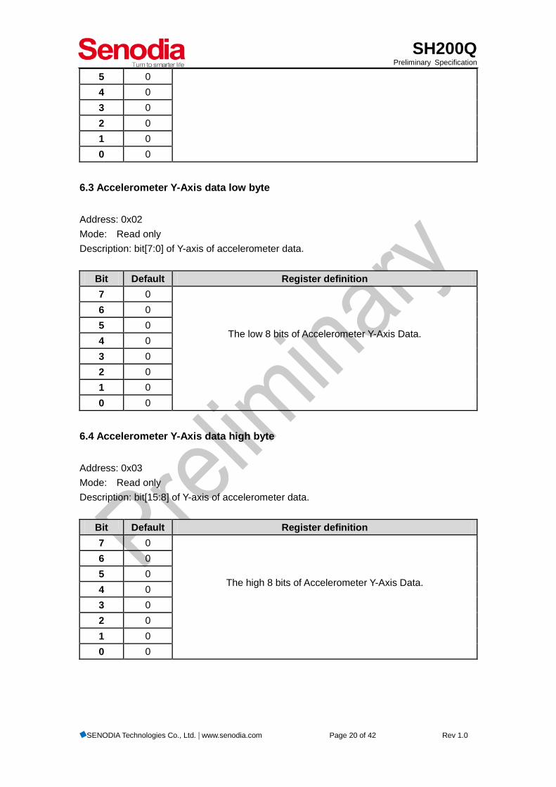
6.3 Accelerometer Y-Axis data low byte
Address: 0x02 Mode: Read only Description: bit[7:0] of Y-axis of accelerometer data.
Bit Default Register definition 7 0
The low 8 bits of Accelerometer Y-Axis Data.
6 0 5 0 4 0 3 0 2 0 1 0 0 0
6.4 Accelerometer Y-Axis data high byte
Address: 0x03 Mode: Read only Description: bit[15:8] of Y-axis of accelerometer data.
Bit Default Register definition 7 0
The high 8 bits of Accelerometer Y-Axis Data.
6 0 5 0 4 0 3 0 2 0 1 0 0 0

SH200Q Preliminary Specification
SENODIA Technologies Co., Ltd. | www.senodia.com Page 21 of 42 Rev 1.0
6.5 Accelerometer Z-Axis data low byte
Address: 0x04 Mode: Read only Description: bit[7:0] of Z-axis of accelerometer data.
Bit Default Register definition 7 0
The low 8 bits of Accelerometer Z-Axis Data.
6 0 5 0 4 0 3 0 2 0 1 0 0 0
6.6 Accelerometer Z-Axis data high byte
Address: 0x05 Mode: Read only Description: bit[15:8] of Z-axis of accelerometer data.
Bit Default Register definition 7 0
The high 8 bits of Accelerometer Z-Axis Data.
6 0 5 0 4 0 3 0 2 0 1 0 0 0
6.7 Gyroscope X-Axis data low byte
Address: 0x06 Mode: Read only Description: bit[7:0] of X-axis of gyroscope data.

SH200Q Preliminary Specification
SENODIA Technologies Co., Ltd. | www.senodia.com Page 22 of 42 Rev 1.0
Bit Default Register definition 7 0
The low 8 bits of Gyroscope X-Axis Data.
6 0 5 0 4 0 3 0 2 0 1 0 0 0
6.8 Gyroscope X-Axis data high byte
Address: 0x07 Mode: Read only Description: bit[15:8] of X-axis of gyroscope data.
Bit Default Register definition 7 0
The high 8 bits of Gyroscope X-Axis Data.
6 0 5 0 4 0 3 0 2 0 1 0 0 0
6.9 Gyroscope Y-Axis data low byte
Address: 0x08 Mode: Read only Description: bit[7:0] of Y-axis of gyroscope data.
Bit Default Register definition 7 0
The low 8 bits of Gyroscope Y-Axis Data.
6 0 5 0 4 0 3 0 2 0

SH200Q Preliminary Specification
SENODIA Technologies Co., Ltd. | www.senodia.com Page 23 of 42 Rev 1.0
1 0 0 0
6.10 Gyroscope Y-Axis data high byte
Address: 0x09 Mode: Read only Description: bit[15:8] of Y-axis of gyroscope data.
Bit Default Register definition 7 0
The high 8 bits of Gyroscope Y-Axis Data.
6 0 5 0 4 0 3 0 2 0 1 0 0 0
6.11 Gyroscope Z-Axis data low byte
Address: 0x0A Mode: Read only Description: bit[7:0] of Z-axis of gyroscope data.
Bit Default Register definition 7 0
The low 8 bits of Gyroscope Z-Axis Data.
6 0 5 0 4 0 3 0 2 0 1 0 0 0
6.12 Gyroscope Z-Axis data high byte
Address: 0x0B Mode: Read only

SH200Q Preliminary Specification
SENODIA Technologies Co., Ltd. | www.senodia.com Page 24 of 42 Rev 1.0
Description: bit[15:8] of Z-axis of gyroscope data.
Bit Default Register definition 7 0
The high 8 bits of Gyroscope Z-Axis Data.
6 0 5 0 4 0 3 0 2 0 1 0 0 0
6.13 Temperature data low byte
Address: 0x0C Mode: Read only Description: bit[7:0] of temperature data.
Bit Default Register definition 7 0
The low 8 bits of Temperature Data.
6 0 5 0 4 0 3 0 2 0 1 0 0 0
6.14 Temperature data high byte
Address: 0x0D Mode: Read only Description: bit[15:8] of temperature data.
Bit Default Register definition 7 0
The high 8 bits of Temperature Data. 6 0 5 0 4 0 3 0

SH200Q Preliminary Specification
SENODIA Technologies Co., Ltd. | www.senodia.com Page 25 of 42 Rev 1.0
2 0 1 0 0 0
6.15 Accelerometer configuration
Address: 0x0E Mode: read/write Description: configuration register of accelerometer
Bit Default Register definition 7 0 1: ACC HPF bypass, 0: ACC HPF valid 6 0 ACC filter clock selector.
1: clock from ADC, 0: internal 1MHz clock 5 0 1: Digital part PDN, 0: normal mode 4 0 ACC output data rate, when bit2 = 0:
00: 1024 Hz 01: 512 Hz 10: 256 Hz 11: 128Hz
ACC output data rate, when bit2 = 1: 00: 64 Hz 01: 32 Hz 10: 16 Hz 11: 8Hz
3 0
2 0 1: Low power mode, ACC sampling rate Fs = 125KHz. ACC filter should be disabled before switch to this mode. 0: normal mode
1 0 1: dither is enabled. 0: dither is disabled.
0 0 1: Accelerator(ACC) filter is enabled. 0: ACC filter is disabled.
6.16 Gyroscope configuration
Address: 0x0F Mode: read/write Description: configuration register of gyroscope
Bit Default Register definition

SH200Q Preliminary Specification
SENODIA Technologies Co., Ltd. | www.senodia.com Page 26 of 42 Rev 1.0
7 0 0: Normal mode. 1: auto power down GYRO when ACC goes to InActive.
6 0 Reserved 5 0 4 0 1: GYRO HPF bypass,
0: GYRO HPF valid 3 0 GYRO output data rate will be:
000: 1000Hz, 001: 500Hz, 010: 250Hz, 011: 31.25Hz 100: 8KHz, 101: 16KHz , 110: 32KHz, 111: Reserved
2 0 1 0
0 0 1: GYRO filter is enabled. 0: GYRO filter is disabled.
6.17 GYRO configuration 1
Address: 0x11 Mode: Read/write Description: configuration of gyroscope
Bit Default Register definition 7 0 reserved 6 0 5 0 00: reserved
01: Get data from GYRO HPF 10: Get data from GYRO IIR Filter. 11: reserved
4 0
3 0 DLPF setting. Low pass filter band width table: DLPF Digital low pass filter bandwidth (Hz)
1000 500 250 31.25 8K 16K 32K 0 250 125 62.5 7.8125 1 200 100 50 6.25 2 100 50 25 3.125 3 50 25 12.5 1.5625 4 25 12.5 6.25 0.78125 5 15 7.5 3.75 0.46875 6 10 5 2.5 0.3125
2 0 1 0 0 0

SH200Q Preliminary Specification
SENODIA Technologies Co., Ltd. | www.senodia.com Page 27 of 42 Rev 1.0
7 5 2.5 1.25 0.15625 8 2K 2K 2K 9 4K 4K 10 8K
6.18 FIFO configuration
Address: 0x12 Mode: Read/write Description: configuration of FIFO
Bit Default Register definition 7 0 Buffer mode selector.
00: No Buffer Mode; 01: FIFO mode
10: Stream Mode; 11: Trigger Mode
6 0
5 0
Hold Level for Trigger Mode.
Water Mark level for FIFO mode.
4 0 3 0 2 0 1 0 0 0
6.19 Interrupt configuration
Address: 0x13 Mode: Read/write Description: configuration of interrupt
Bit Default Register definition 7 0 0: INT output is active high.
1: INT output is active low. 6 0 0: interrupt output is latched.
1: interrupt output is non-latched. 5 0 0: Pin INT is normal output pad
1: Pin INT is open-drain pad 4 0 1: any register read operation will clear interrupt.
0: interrupt status register read will clear interrupt. 3 0 1: any register read will clear ACT interrupt.
0: INT status register read will clear ACT interrupt.

SH200Q Preliminary Specification
SENODIA Technologies Co., Ltd. | www.senodia.com Page 28 of 42 Rev 1.0
2 0 Reserved 1 0 0 0
6.20 Interrupt enable
Address: 0x14 Mode: Read/write Description: configuration of interrupt
Bit Default Register definition 7 0 Reserved 6 0 5 0 1: GYRO data ready interrupt enable
0: GYRO data ready interrupt disable 4 0 1: GYRO watermark interrupt enable
0: GYRO Watermark interrupt disable 3 0 1: ACC watermark interrupt enable
0: ACC watermark interrupt disable 2 0 1: Free-Fall interrupt enable
0: Free-Fall interrupt disable 1 0 1: Activityinterrupt enable
0: Activity interrupt disable 0 0 1: In-Activityinterrupt enable
0: In-Activity interrupt disable
6.21 Accelerometer data format
Address: 0x16 Mode: Read/write Description: configuration of accelerometer data format
Bit Default Register definition 7 0 Reserved 6 0 5 0 4 0 Reserved 3 0 Reserved 2 0 Link ACT/In-ACT status.
0: one time ACT/In-ACT will trigger INT no matter what previous status is. 1: if the previous status is activity, two times In-ACT are needed to

SH200Q Preliminary Specification
SENODIA Technologies Co., Ltd. | www.senodia.com Page 29 of 42 Rev 1.0
generate In-ACT interrupt. If the previous status is inactivity, two times ACT are needed to generate ACT interrupt.
1 0 ACC full scale range. 00: 4G 01: 8G 10: 16G 11: Reserved
0 0
6.22 ACT thresh
Address: 0x17 Mode: Read/write Description: configuration of activity interrupt threshold
Bit Default Register definition 7 0 The threshold value for detecting activity.
The threshold value of activity event detection is: ACT thresh *8 mg in 4g-range, ACT thresh *16 mg in 8g-range, ACT thresh * 32 mg in 16g-range.
6 0 5 0 4 0 3 0 2 0 1 0 0 0
6.23 InACT thresh
Address: 0x18 Mode: Read/write Description: configuration of inactivity interrupt threshold
Bit Default Register definition 7 0 The threshold value for detecting inactivity.
The threshold value of in-activity event detection is: InACT thresh *8 mg in 4g-range, InACT thresh *16 mg in 8g-range, InACT thresh * 32 mg in 16g-range.
6 0 5 0 4 0 3 0 2 0 1 0

SH200Q Preliminary Specification
SENODIA Technologies Co., Ltd. | www.senodia.com Page 30 of 42 Rev 1.0
0 0
6.24 ACT time thresh
Address: 0x19 Mode: Read/write Description: configuration of the amount of samples that acceleration must be greater than the value in the register 0x17 for activity to be declared
Bit Default Register definition 7 0
The amount of samples that acceleration must be greater than the value in the register 0x17 for activity to be declared.
6 0 5 0 4 0 3 0 2 0 1 0 0 0
6.25 InACT time thresh
Address: 0x1A Mode: Read/write Description: configuration of the amount of time that acceleration must be less than the value in the register 0x18 for inactivity to be declared.
Bit Default Register definition 7 0
The amount of time that acceleration must be less than the value in the register 0x18 for inactivity to be declared.
The Time of InACT time thresh is in unit of second.
6 0 5 0 4 0 3 0 2 0 1 0 0 0

SH200Q Preliminary Specification
SENODIA Technologies Co., Ltd. | www.senodia.com Page 31 of 42 Rev 1.0
6.26 ACT-InACT configuration
Address: 0x1B Mode: Read/write Description: configuration of the activity and inactivity interrupt control.
Bit Default Register definition 7 0 1: Act interrupt detect by ac data
0: Act interrupt detect by dc data 6 0 1: X-axis ACT interrupt enable.
0: X-axis ACT interrupt disable. 5 0 1: Y-axis ACT interrupt enable.
0: Y-axis ACT interrupt disable. 4 0 1: Z-axis ACT interrupt enable.
0: Z-axis ACT interrupt disable. 3 0 1: InACT interrupt detect by ac data
0: InACT interrupt detect by dc data 2 0 1: X-axis InACT interrupt enable.
0: X-axis InACT interrupt disable. 1 0 1: Y-axis InACT interrupt enable.
0: Y-axis InACT interrupt disable. 0 0 1: Z-axis InACT interrupt enable.
0: Z-axis InACT interrupt disable.
6.27 Free-Fall threshold
Address: 0x1C Mode: Read/write Description: configurations of the threshold of free-fall interrupt.
Bit Default Register definition 7 0 Free-Fall threshold.
The threshold value of Free-Fall event detection is:
ThreshFF *16 mg in 4g-range, ThreshFF *32 mg in 8g-range, ThreshFF *64 mg in 16g-range,
6 0 5 0 4 0 3 0 2 0 1 0 0 0

SH200Q Preliminary Specification
SENODIA Technologies Co., Ltd. | www.senodia.com Page 32 of 42 Rev 1.0
6.28 Free-Fall Time Threshold
Address: 0x1D Mode: Read/write Description: configurations of minimum time that the value of all axes must be less than the value in register 0x1C to generate a free-fall interrupt.
Bit Default Register definition 7 0
Minimum time that the value of all axes must be less than the value in register 0x1C to generate a free-fall interrupt.
The time required to trigger free-fall interrupt is Time_FF * 2
milliseconds.
6 0 5 0 4 0 3 0 2 0 1 0 0 0
6.29 Interrupt count limit
Address: 0x1E Mode: Read/write Description: configuration of the interrupt pulse width when 0x13 bit 6 is set to ‘1’.
Bit Default Register definition 7 0
INT Count Limit. When register 0x13 bit 6 is high, INT will be auto-cleared when
interrupt last time is more than defined in this register. This counter is based on 250Hz clock.
6 0 5 0 4 0 3 0 2 0 1 0 0 0
6.30 Gyroscope full scale range
Address: 0x2B Mode: Read/write Description: configuration of the full scale range of gyroscope

SH200Q Preliminary Specification
SENODIA Technologies Co., Ltd. | www.senodia.com Page 33 of 42 Rev 1.0
Bit Default Register definition 7 0
Reserved 6 0 5 0 4 0 3 0 2 0 Precision[2:0]: Full Scale Range
000 2000 001 1000 010 500 011 250 100 125
Others reserved
1 0 0 0
6.31 Interrupt status
Address: 0x2C Mode: Read only Description: interrupt status register
Bit Default Register definition 7 0 0 6 0 0 5 0 1: Data is Ready
0: Data is not Ready 4 0 1: the valid data in gyroscope FIFO exceeds the watermark value
when FIFO mode. 0: the valid data in gyroscope FIFO doesn’t exceed the watermark value when FIFO mode.
3 0 1: the valid data in accelerometer FIFO exceeds the watermark value when FIFO mode. 0: the valid data in accelerometer FIFO doesn’t exceed the watermark value when FIFO mode.
2 0 1: Free-Fall interrupt has been detected. 0: Free-Fall interrupt has not been detected.
1 0 1: activity interrupt has been detected. 0: activity interrupt has not been detected.
0 0 1: in-activity interrupt has been detected. 0: in-activity occurred has not been detected.

SH200Q Preliminary Specification
SENODIA Technologies Co., Ltd. | www.senodia.com Page 34 of 42 Rev 1.0
6.32 Act-InACT status
Address: 0x2D Mode: Read only Description: activity and inactivity interrupts status and sign for each axis of accelerometer.
Bit Default Register definition 7 0 activity or inactivity Sign 6 0 activity or inactivity interrupt has been detected in accelerometer
X-axis 5 0 activity or inactivity interrupt has been detected in accelerometer
Y-axis 4 0 activity or inactivity interrupt has been detected in accelerometer
Z-axis 3 0 0 2 0 0 1 0 0 0 0 0
6.33 accelerometer FIFO Status
Address: 0x2E Mode: Read only Description: accelerometer FIFO status registers
Bit Default Register definition 7 0 1: Accelerometer FIFO is Full
0: Accelerometer FIFO is not Full 6 0 1: Accelerometer FIFO is Empty
0: Accelerometer FIFO is not empty. 5 0
Accelerometer FIFO valid data samples
4 0 3 0 2 0 1 0 0 0
6.34 Gyroscope FIFO Status
Address: 0x2F Mode: Read only Description: gyroscope FIFO status registers

SH200Q Preliminary Specification
SENODIA Technologies Co., Ltd. | www.senodia.com Page 35 of 42 Rev 1.0
Bit Default Register definition 7 0 1: gyroscope FIFO is Full.
0: gyroscope FIFO is not full. 6 0 1: gyroscope FIFO is Empty
0: gyroscope FIFO is not Empty. 5 0
gyroscope FIFO valid data samples.
4 0 3 0 2 0 1 0 0 0
6.35 chip ID
Address: 0x30 Mode: Read only Description: chip ID of SH200Q
Bit Default Register definition 7 0
8’b0001_1000
6 0 5 0 4 1 3 1 2 0 1 0 0 0
7 Application Information
7.1 Orientation of Axes
The diagram below shows the orientation of the axes of sensitivity and the polarity of rotation. Note the pin 1 marker in the figure.

SH200Q Preliminary Specification
SENODIA Technologies Co., Ltd. | www.senodia.com Page 36 of 42 Rev 1.0
Figure 7.1.Orientation of Axes Sensitivity and Polarity of Rotation
7.2 Typical Application Circuit
4
5
6
18
17
16
15
14
13
24 23 22 21 20 19
7 8 9 10 11 12
Top View
NC
NC
2
1
3
SDA
RES
V
SCK
NC
NC
NC
NC
NC
NC
NC
NC
MSD
A
GND
VDD
INT
NC
MC
LK
VDD
IO
0.1uF
RES
V
RES
V
SEN
BSD
O
0.1uF
4.7kΩ4.7kΩ
SDA
SCK
SA0
VDD
INT
Figure 7.2.1: Reference Application Circuitry using I2C interface
+x
+y +z
gravity
Ωz
Ωy
Ωx

SH200Q Preliminary Specification
SENODIA Technologies Co., Ltd. | www.senodia.com Page 37 of 42 Rev 1.0
4
5
6
18
17
16
15
14
13
24 23 22 21 20 19
7 8 9 10 11 12
Top View
NC
NC
2
1
3SD
A
RES
V
SCK
NC
NC
NC
NC
NC
NC
NC
NC
MSD
A
GND
VDD
INT
NC
MC
LK
VDD
IO
0.1uFR
ESV
RES
V
SEN
BSD
O
0.1uF
4.7kΩ4.7kΩ
MOSI
SCK
CSB
MISO
VDD
INT
Figure 7.2.2: Reference Application Circuitry using SPI 4-wire interface 7.3 Package Outline Dimensions
7.3.1 QFN Package Outline Dimensions

SH200Q Preliminary Specification
SENODIA Technologies Co., Ltd. | www.senodia.com Page 38 of 42 Rev 1.0
Figure 7.3.1: QFN Package Outline Dimensions
7.4 Package laser Mark
Figure 7.4.1: QFN Package laser Mark

SH200Q Preliminary Specification
SENODIA Technologies Co., Ltd. | www.senodia.com Page 39 of 42 Rev 1.0
7.5 Packing of the Chips SH200Q packing in Tape & Reel (7’’), and meet EIA-481 standard.
7.5.1 Packing direction
Figure 7.5.1: Packing direction 7.6 Labels
Fig. 7.6: Label sample
7.7 Packing

SH200Q Preliminary Specification
SENODIA Technologies Co., Ltd. | www.senodia.com Page 40 of 42 Rev 1.0
Fig. 7.7: packing of product 7.8 Solder Reflow Curve Solder Reflow curve follows IPC/JEDEC J-STD-020 Pb-free standards.
7.8.1 Solder Reflow curve

SH200Q Preliminary Specification
SENODIA Technologies Co., Ltd. | www.senodia.com Page 41 of 42 Rev 1.0
Figure 7.8: Solder Reflow curve
7.9 Storage condition The storage condition follows JEDEC J-STD-020, MSL3.
8. Reliability
8.1 Reliability standard:
SH200Q reliability test plan follows JEDEC 47Istandards, “Stress-Test-Driven Qualification of Integrated Circuits”.

SH200Q Preliminary Specification
SENODIA Technologies Co., Ltd. | www.senodia.com Page 42 of 42 Rev 1.0
9. Environment Compliant SH200Q pass SGS certification,compliant with RoHS standards.
10 Revision History
Date Revision Changes 2017-7-28 1.0 Preliminary version.
11. Disclaimer Information furnished by SENODIA is believed to be accurate and reliable. However, SENODIA reserve the right to make changes, modifications or corrections to this document and related products at any time, without notice. No license and intellectual property right is granted under this document. We reserve all rights of disposal such copying or passing on to third parties. No responsibility is assumed by SENODIA for any infringements of patents or other rights of third parties which may result from its use.