4 mhz dsp lock-in amplifiersr865a dsp lock-in amplifier certification stanford research systems...
TRANSCRIPT

Revision 2.07
Operation Manual
SR865A 4 MHz DSP Lock-in Amplifier
SR865A DSP Lock-in Amplifier
Certification Stanford Research Systems certifies that this product met its published specifications at the time of shipment.
Warranty This Stanford Research Systems product is warranted against defects in materials and workmanship for a period of one (1) year from the date of shipment.
Service For warranty service or repair, this product must be returned to a Stanford Research Systems authorized service facility. Contact Stanford Research Systems or an authorized representative before returning this product for repair.
Information in this document is subject to change without notice. Copyright © Stanford Research Systems, Inc., 2015–2019. All rights reserved. Stanford Research Systems, Inc. 1290-C Reamwood Avenue Sunnyvale, California 94089 www.thinkSRS.com Printed in U.S.A. Document number 9-01715-903

Safety and Preparation For Use i
SR865A DSP Lock-in Amplifier
Safety and Preparation for Use Warning
Dangerous voltages, capable of causing injury or death, are present in this instrument. Use extreme caution whenever the instrument covers are removed. Do not remove the covers while the unit is plugged into a live outlet.
Line Voltage Selection Caution This instrument may be damaged if operated with the LINE VOLTAGE SELECTOR set for the wrong ac line voltage or if the wrong fuse is installed.
The SR865A operates from a 100V, 120V, 220V, or 240V nominal ac power source having a line frequency of 50 or 60 Hz. Before connecting the power cord, verify that the LINE VOLTAGE SELECTOR card, located in the rear panel fuse holder, is set so that the correct ac input voltage value is indicated by the white dot.
Conversion to other ac input voltages requires a change in the voltage selector card position and fuse value. See Appendix F (page 179) for detailed instructions.
Line Fuse Verify that the correct line fuse is installed before connecting the line cord. For 100V/120V, use a 1 Amp fuse and for 220V/240V, use a 1/2 Amp fuse. See Appendix F (page 179) for detailed fuse installation instructions.
Line Cord The SR865A has a detachable, three-wire power cord for connection to the power source and to a protective ground. The exposed metal parts of the instrument are connected to the outlet ground to protect against electrical shock. Always use an outlet which has a properly connected protective ground. Power Cord
Grounding A chassis grounding lug is available on the back panel of the SR865A. Connect a heavy duty ground wire, #12AWG or larger, from the CHASSIS GROUND lug directly to a facility earth ground to provide additional protection against electrical shock.
Grounded BNC shields are connected to the chassis ground. Do not apply any voltage to the grounded shields. The A and B signal input shields are connected to chassis ground through resistors and can tolerate up to 1 V of applied voltage.
GFCI (Ground Fault Circuit Interrupter) GFCI protected outlets are often available in production and laboratory environments, particularly in proximity to water sources. GFCI’s are generally regarded as an important defense against electrocution. However, the use of GFCI in conjunction with the SR865A

ii Safety and Preparation For Use
SR865A DSP Lock-in Amplifier
must not be regarded as a substitute for proper grounding and careful system design. GFCI’s must also be tested regularly to verify their functionality. Always consult an electrician when in doubt.
Service Do not attempt to service this instrument unless another person, capable of providing first aid or resuscitation, is present.
Do not install substitute parts or perform any unauthorized modifications to this instrument. Contact the factory for instructions on how to return the instrument for authorized service and adjustment.
Warning Regarding Use With Photomultipliers and Other Detectors
The front end amplifier of this instrument is easily damaged if a photomultiplier is used improperly with the amplifier. When left completely unterminated, a cable connected to a PMT can charge to several hundred volts in a relatively short time. If this cable is connected to the inputs of the SR865A the stored charge may damage the front-end amplifier. To avoid this problem, always discharge the cable and connect the PMT output to the SR865A input before turning the PMT on.
Furnished Accessories • Power Cord • Operating Manual
Environmental Conditions Operating Temperature: +10 °C to +40 °C (Specifications apply over +18 °C to +28 °C) Relative Humidity: <90 % Non-condensing
Non-Operating Temperature: −25°C to 65°C Humidity: <95 % Non-condensing

Safety and Preparation For Use iii
SR865A DSP Lock-in Amplifier

iv Safety and Preparation For Use
SR865A DSP Lock-in Amplifier

Contents v
SR865A DSP Lock-in Amplifier
Contents Safety and Preparation for Use i Contents v SR865A Specifications vii SR865A Command List x SR865A Status Bytes xv
Chapter 1 Getting Started 1 Introduction 1 SR865A Front Panel 2 SR865A Touchscreen 4 The Basic Lock-in 9 Using Displays 13 Sensitivity, Offset and Expand 20 Saving and Recalling Setups 25 Aux Outputs and Inputs 28 Scanning 30
Chapter 2 Lock-in Amplifier Basics 37 What is a Lock-in Amplifier? 37 What Does a Lock-in Measure? 40 Block diagram 41 The Reference Oscillator 42 The Phase Sensitive Detectors 43 Time Constants and Sensitivity 44 Outputs and Scales 46 What is Dynamic Reserve Really? 48 The Input Amplifier 50 Input Connections 51 Intrinsic (Random) Noise Sources 54 External Noise Sources 55 Noise Measurements 58
Chapter 3 Operation 61 Introduction 61 Standard Settings 64 Signal Input 65 CH1 and CH2 Outputs: Offset, Ratio and Expand 71 Reference 74 Display 81 Cursor 83

vi Contents
SR865A DSP Lock-in Amplifier
Functions 85 Interface and Data 87 Setup 88 Rear Panel 96
Chapter 4 Programming 101 Introduction 101 Command Syntax 103 Reference Commands 106 Signal Commands 111 CH1/CH2 Output Commands 114 Aux Input and Output Commands 116 Auto Function Commands 117 Display Commands 118 Strip Chart Commands 120 FFT Screen Commands 125 Scan Commands 128 Data Transfer Commands 132 Data Capture Commands 134 Data Streaming Commands 140 System Commands 143 Interface Commands 146 Status Reporting Commands 148 Status Byte Definitions 151
Appendix A Advanced Filters 155
Appendix B The FFT Display 161
Appendix C Using the Webserver 169
Appendix D Data Streaming and Capture 171
Appendix E Dual Reference Detection 175
Appendix F Fuse Installation and ac Line Select 179
Appendix G Performance Tests 183
Appendix H Circuit Description 203

Specifications vii
SR865A DSP Lock-in Amplifier
SR865A Specifications Signal Channel
Voltage Inputs Single-ended (A) or differential (A−B) Sensitivity (Output Scale) 1 nV to 1 V (voltage input) 1 fA to 1 µA (current input) Input Impedance 10 MΩ+25 pF, ac (>1 Hz) or dc coupled Input Range 10 mV to 1 V (peak); max input before overload Gain Accuracy 1% below 200 kHz and 2% to 4 MHz (signal amplitude <30% of input range) Input Noise 2.5 nV/√Hz above 1 kHz, 10 mV input range (typical) CMRR Greater than 90 dB at 1 kHz (dc Coupled, 10 mV to 100 mV input range) Harmonic Distortion −80 dB below 100 kHz, −60 dB above 100 kHz Dynamic Reserve Greater than 120 dB Current Input Ranges 1 μA or 10 nA
Reference Channel Frequency Range 1 mHz to 4 MHz Timebase 10 MHz In/Out phase locks the internal frequency to other SR865A units Ext TTL Reference Minimum 2 V logic level, rising or falling edge Ext Sine Reference 400 mV pk–pk minimum signal, ac coupled (>1 Hz) Ext Reference Input Impedance 1 MΩ or 50 Ω Acquisition Time (2 cycles + 5 ms) or 40 ms, whichever is greater Phase Setting Resolution 360/232 deg Phase Noise Ext TTL reference: <0.001° rms at 1 kHz, (100 ms, 12 dB/oct) (typical) Internal reference: <0.0001° rms at 1 kHz (100 ms, 12 dB/oct) Phase Drift Sine Out to Signal In (200 mVrms) <0.002°/°C below 20 kHz (dc coupled input) <0.02°/°C below 200 kHz <0.2°/°C below 2 MHz Harmonic Detect Detect at N×fref where N≤99 and N×fref<4 MHz Dual F Reference Detect at fdual = | fint − fext | All frequencies less than 4 MHz for specified performance Chopper Reference SR865A drives SR540 Chopper (via Aux Out 4) to lock the chopper to fint
Demodulator dc Stability Digital output values have no offset drift Time Constants 1 µs to 30 ks Low Pass Filters Typical RC type filters or Advanced Gaussian/Linear Phase filters Filter Slope 6, 12, 18, 24 dB/oct rolloffs Synchronous Filter Available below 4 kHz Harmonic Rejection −80 dB Low Latency Output Rear panel BlazeX output with <2 µs delay (plus low pass filter rise/fall times)
Internal Oscillator Frequency 1 mHz to 4 MHz Frequency Accuracy 25 ppm + 30 µHz with internal timebase External Timebase 10 MHz timebase input/output on rear panel Frequency Resolution 6 digits or 0.1 mHz, whichever is greater

viii Specifications
SR865A DSP Lock-in Amplifier
Sine Output Outputs Differential or Single-ended Output Impedance 50 Ω source Amplitude 1 nVrms to 2 Vrms (specified amplitude is differential into 50 Ω loads) Output amplitude is halved when used single-ended Output amplitude is doubled into a high impedance load Amplitude Resolution 3 digits or 1 nV, whichever is greater dc Offset ±5 V, differential or common mode Offset Resolution 3 digits or 0.1 mV, whichever is greater Output Limit ±6 V, sum of dc offset and peak amplitude Sync Logic level sync on rear panel (via BlazeX output)
Data Data Channels 4 data channels are displayed and graphed (green, blue, yellow, orange) Data Sources Each data channel can be assigned any of these data sources:
X, Y, R, θ, Aux In 1–4, Aux Out 1–2, Xnoise, Ynoise, Sine Out Amplitude, Sine Out DC Level, reference phase, fint or fext
Data History All data sources are continuously stored at all chart display time scales. The complete stored history of any data source can be displayed at any time.
Offset X, Y and R may be offset up to ±999% of the sensitivity Ratio X, and Y may be ratioed by Aux In 3; R may be ratioed by Aux In 4 Expand X, Y and R may be expanded by ×10 or ×100 Capture Buffer 1 Mpoints internal data storage. Store (X), (X and Y), (R and θ) or (X, Y, R and θ)
at sample rates up to 1.25 MHz. This is in addition to the data histories for the chart display.
Data Streaming Realtime streaming of data, either (X), (X and Y), (R and θ) or (X, Y, R and θ) at sample rates up to 1.25 MHz over Ethernet interface
Scanning One of the following parameters may be scanned: fint, Sine Out Amplitude, Sine Out DC Level, Aux Out 1 or 2.
FFT Source Input ADC, demodulator output, or filter output Record length 1024 bins Averaging exponential rms
Inputs and Outputs CH 1 Output Proportional to X or R, ±10 V full scale thru 50 Ω CH 2 Output Proportional to Y or θ, ±10 V full scale thru 50 Ω X and Y Outputs Proportional to X and Y, ±10 V full scale thru 50 Ω, rear panel BlazeX Low latency output of X, ±2.0 V full scale or
logic level reference sync output, either thru 50 Ω Aux Outputs 4 BNC D/A outputs, ±10.5 V thru 50 Ω, 1 mV resolution Aux Inputs 4 BNC A/D inputs, ±10.5 V, 1 mV resolution, 1 MΩ input Trigger Input TTL input triggers storage into the internal capture buffer Monitor Output Analog output of the signal amplifier HDMI Video output to external monitor or TV, 640x480/60 Hz. Timebase Input/Output 1 Vrms 10 MHz clock to synchronize internal reference frequency to other units

Specifications ix
SR865A DSP Lock-in Amplifier
General Interfaces IEEE488, RS-232, USB device (Test and Measurement Class) and Ethernet
(VXI-11 and telnet) USB Flash Front panel slot for USB flash storage of screen shots and data, and firmware
upgrades Preamp Power 9 pin D connector to power SRS preamps Power 60 Watts, 100/120/220/240 VAC, 50/60 Hz Dimensions 17"W × 5.25"H × 17"D Weight 22 lbs Warranty One year parts and labor on materials and workmanship

x Commands
SR865A DSP Lock-in Amplifier
SR865A Command List Reference Commands page description
TBMODE(?) AUTO | INternal | i 106 Set the 10 MHz timebase TBSTAT? 106 Query the current 10 MHz timebase ext (0) or int (1) PHAS(?) p UDEG | MDEG | DEG | URAD | MRAD | RAD 106 Set the reference phase to p APHS 106 Auto Phase FREQ(?) f HZ | KHZ | MHZ 106 Set the reference frequency to f FREQINT(?) f HZ | KHZ | MHZ 107 Set the internal reference frequency to f FREQEXT? 107 Query the external reference frequency FREQDET? 107 Query the detection frequency HARM(?) i 107 Set harmonic detect to i HARMDUAL(?) i 107 Set harmonic for dual reference mode to i BLADESLOTS(?) SLT6 | SLT30 | i 108 Set the chopper blade number of slots BLADEPHASE(?) p UDEG | MDEG | DEG | URAD | MRAD | RAD
108 Set the chopper blade phase to p
SLVL(?) v NV | UV | MV | V 108 Set sine output amplitude to v SOFF(?) v NV | UV | MV | V 108 Set sine output dc level to v REFM(?) COMmon | DIFference | i 109 Set sine output dc mode RSRC(?) INT | EXT | DUAL | CHOP | i 109 Set reference mode RTRG(?) SIN | POSttl | NEGttl | i 109 Set external reference trigger REFZ(?) 50ohms | 1Meg | i 109 Set external reference input impedance PSTF(?) [ j ] , f HZ | KHZ | MHZ 110 Set frequency preset j to f PSTA(?) [ j ] , v NV | UV | MV | V 110 Set sine amplitude preset j to v PSTL(?) [ j ] , v NV | UV | MV | V 110 Set sine dc level preset j to v Signal Commands page description
IVMD(?) VOLTage | CURRent | i 111 Set input to voltage/current ISRC(?) A | A−B | i 111 Set voltage input configuration ICPL(?) AC | DC | i 111 Set voltage input coupling IGND(?) FLOat | GROund | i 111 Set voltage input shield grounding IRNG(?) 1Volt | 300Mvolt | 100Mvolt | 30Mvolt | 10Mvolt | i 111 Set voltage input range ICUR(?) 1MEG | 100MEG | i 112 Set current input gain ILVL? 112 Query the signal strength low to overload (0–4) SCAL(?) i 112 Set sensitivity from 1V (0) to 1 nV (27) OFLT(?) i 113 Set time constant from 1 μs (0) to 30 ks (21) OFSL(?) i 113 Set filter slope from 6 dB (0) to 24 dB (3) SYNC(?) OFF | ON | i 113 Turn synchronous filter off/on ADVFILT(?) OFF | ON | i 113 Turn advanced filtering off/on ENBW? 113 Query the equivalent noise bandwidth

Commands xi
SR865A DSP Lock-in Amplifier
CH1/CH2 Output Commands page description
COUT(?) [ OCH1 | OCH2 | j ] , XY | RTHeta | i 114 Set CH1/2 to (X or R)/(Y or θ) CEXP(?) [ X | Y | R | j ] , OFF | X10 | X100 | i 114 Set CH1/2 expand COFA(?) [ X | Y | R | j ] , OFF | ON | i 114 Turn CH1/2 output offset off/on COFP(?) [ X | Y | R | j ] , x 114 Set CH1/2 output offset to x percent OAUT [ X | Y | R | j ] 114 Auto Offset CH1/2 CRAT(?) [ X | Y | R | j ] , OFF | ON | i 115 Ratio Ch1/2 with Aux In 3 or 4 Aux Input and Output Commands page description
OAUX? [ j ] 116 Query Aux Input j (0–3) AUXV(?) [ j ] , v NV | UV | MV | V 116 Set Aux Output j (0–3) voltage to v Auto Function Commands page description
APHS 117 Auto Phase ARNG 117 Auto Range ASCL 117 Auto Scale Display Commands page description
DBLK(?) OFF | ON | i 118 Turn front panel blanking off/on DLAY(?) TREnd | HISTory | BARHist | FFT | BARFft | BAREight | i 118 Set Screen Layout DCAP 118 Screen Shot to USB memory stick CDSP(?) [ DAT1 | DAT2 | DAT3 | DAT4 | j ] , parameter | i 118 Assign parameter i to data channel j CGRF(?) [ DAT1 | DAT2 | DAT3 | DAT4 | j ] , OFF | ON | i 119 Turn data channel j strip graph off/on GETSCREEN? 119 Download screen capture image Strip Chart Commands page description
GSPD(?) i 120 Set horizontal scale from 0.5 s (0) to 2 days (16) GSCL(?) [ DAT1 | DAT2 | DAT3 | DAT4 | j ] , x 120 Set channel j vertical scale to x GOFF(?) [ DAT1 | DAT2 | DAT3 | DAT4 | j ] , x 120 Set channel j vertical offset GAUT [ DAT1 | DAT2 | DAT3 | DAT4 | j ] 121 Auto scale channel j GACT [ DAT1 | DAT2 | DAT3 | DAT4 | j ] 121 Auto scale with zero center channel j GAUF [ DAT1 | DAT2 | DAT3 | DAT4 | j ] 121 Auto find for channel j CGRF(?) [ DAT1 | DAT2 | DAT3 | DAT4 | j ] , OFF | ON | i 121 Turn channel j graph off/on GLIV(?) OFF | ON | i 122 Turn strip chart off/on (pause/run) PCUR(?) i 122 Move cursor to i (0=right, 639=left) CURREL(?) OFF | ON | i 122 Set cursor relative or absolute mode CURDISP(?) i 122 Set cursor horizontal mode to date/time or interval CURBUG(?) AVG | MAX | MIN | i 122 Set cursor to mean / maximum / minimum FCRW(?) LIne | NARrow | WIde | i 123 Set the cursor width SCRY? [ DAT1 | DAT2 | DAT3 | DAT4 | STATus | j ] 123 Query the cursor data values CURDATTIM? 123 Query the cursor horizontal position as date/time CURINTERVAL? 124 Query the cursor horizontal position as interval

xii Commands
SR865A DSP Lock-in Amplifier
FFT Screen Commands page description
FFTR(?) ADC | MIXer | FILTer | i 125 Set FFT data source FFTS(?) i 125 Set vertical scale from 1.0 dB (0) to 200 dB (7) FFTO(?) x 125 Set top reference level FAUT 126 FFT auto scale FFTMAXSPAN? 126 Query maximum allowed frequency span in Hz/div FFTSPAN(?) x 126 Set frequency span in Hz/div FFTA(?) AVG1 | AVG3 | AVG10 | AVG30 | AVG100 | i 126 Set averaging FFTL(?) OFF | ON | i 126 Turn FFT off/on (pause/live) FCRW(?) LIne | NARrow | WIde | i 126 Set the cursor width FCRX? 127 Query the FFT cursor frequency FCRY? 127 Query the FFT cursor amplitude Scan Commands page description SCNPAR(?) Fint | REFAmp | REFDc | OUT1 | OUT2 | i 128 Set the scan parameter SCNLOG(?) LIN | LOG | i 128 Set the scan type SCNEND(?) ONce | REpeat | UPdown | i 128 Set the scan end mode SCNSEC(?) x 128 Set the scan time to x seconds SCNAMPATTN(?) i 128 Set the amplitude attenuator mode for scanning SCNDCATTN(?) i 129 Set the dc attenuator mode for scanning SCNINRVL(?) i 129 Set the scan parameter update interval SCNENBL(?) OFF | ON | i 129 Turn the scan off/on SCNRUN 130 Start or resume the scan SCNPAUSE 130 Pause the scan SCNRST 130 Reset the scan SCNSTATE? 130 Query the scan (off, reset, run, pause or done)(0-4) SCNFREQ(?) [ BEGin | END | j ] , f HZ | KHZ | MHZ 130 Set the begin/end frequency SCNAMP(?) [ BEGin | END | j ] , v NV | UV | MV | V 130 Set the begin/end reference amplitude SCNDC(?) [ BEGin | END | j ] , v NV | UV | MV | V 130 Set the begin/end reference dc level SCNAUX1(?) [ BEGin | END | j ] , v NV | UV | MV | V 131 Set the begin/end AuxOut1 value SCNAUX2(?) [ BEGin | END | j ] , v NV | UV | MV | V 131 Set the begin/end AuxOut2 value Data Transfer Commands page description
OUTR? [ DAT1 | DAT2 | DAT3 | DAT4 | j ] 132 Query data channel j OUTP? [ j ] 132 Query lock-in parameter j SNAP? [ j, k ] , l 132 Query multiple lock-in parameters at once SNAPD? 133 Query all 4 displayed parameters at once Data Capture Commands page description
CAPTURELEN(?) n 136 Set the buffer length to n 1 kbyte blocks CAPTURECFG(?) X | XY | RT | XYRT | i 136 Configure capture to X, XY, Rθ or XYRθ (0–3) CAPTURERATEMAX? 137 Query the maximum capture rate

Commands xiii
SR865A DSP Lock-in Amplifier
CAPTURERATE(?) n 137 Set the capture rate to (max rate)/2n CAPTURESTART [ ONEshot | CONTinuous | i ] , [ IMMediate | TRIGstart | SAMPpertrig | j ]
137 Start capture (OneShot or Cont) (HW trigger off/on)
CAPTURESTOP
138 Stop capture
CAPTURESTAT? 138 Query the capture buffer state CAPTUREBYTES? 138 Query the number of bytes filled by captured data CAPTUREPROG? 139 Query the length (kB) of captured data (after stop) CAPTUREVAL? [ n ] 139 Query the nth sample (1, 2 or 4 values) (after stop) CAPTUREGET? [ i ], [ j ] 139 Download binary capture buffer Data Streaming Commands page description
STREAMCH(?) X | XY | RT | XYRT | i 140 Configure streaming to X, XY, Rθ or XYRθ (0–3) STREAMRATEMAX? 141 Query the maximum streaming rate STREAMRATE(?) n 141 Set the streaming rate to (max rate)/2n STREAMFMT(?) i 141 Set the streaming format to float32 (0) or int16 (1) STREAMPCKT(?) i 141 Set packet size to 1024, 512, 256 or 128 bytes (0–3) STREAMPORT(?) i 142 Sets the Ethernet port to i=1024–65535 STREAMOPTION(?) i 142 Sets big/little endianness and integrity checking STREAM(?) OFF | ON | i 142 Turn streaming off/on System Commands page description
TIME(?) [ SEConds | MINutes | HOUrs | j ] , i 143 Set time DATE(?) [ DAY | MONth | YEAr | j ] , i 143 Set date TBMODE(?) AUTO | INternal | i 143 Set the 10 MHz timebase TBSTAT? 143 Query the current 10 MHz timebase ext (0) or int (1) BLAZEX(?) BLazex | BIsync | UNIsync | i 143 Select the BlazeX output KEYC(?) ON | MUte| i 144 Turn sounds on or off PRMD(?) SCReen | PRNt | MONOchrome | i 144 Set screen shot mode SDFM(?) CSV | MATfile | i 144 Set data file type FBAS(?) s 144 Set file name prefix FNUM(?) i 144 Set file name suffix FNXT? 145 Query next file name DCAP 145 Screen shot SVDT 145 Save data
Interface Commands page description
*RST 146 Reset the unit to its default configuration *IDN? 146 Query the unit identification string *TST? 146 No-op, returns “0” *OPC(?) 146 Operation Complete LOCL(?) i 146 Set LOCAL (0), REMOTE (1) or LOCKOUT (2)

xiv Commands
SR865A DSP Lock-in Amplifier
OVRM (?) OFF | ON | i 147 Set GPIB Overide Remote off (0) or on (1) Status Reporting Commands page description
*CLS 148 Clear all status bytes *ESE(?) j, i 148 Set the standard event enable register *ESR? j 148 Query the standard event status byte *SRE(?) j, i 148 Set the serial poll enable register *STB? j 148 Query the serial poll status byte *PSC(?) i 149 Set the Power-On Status Clear bit ERRE(?) j, i 149 Set the error status enable register ERRS? j 149 Query the error status byte LIAE(?) j, i 149 Set LIA status enable register LIAS? j 150 Query the LIA status word CUROVLDSTAT? 150 Query the present overload states

Commands xv
SR865A DSP Lock-in Amplifier
SR865A Status Bytes Serial Poll Status Byte bit name usage 0 unused 1 unused 2 ERR An enabled bit in the error status byte has been set 3 LIA An enabled bit in the LIA status byte has been set 4 MAV The interface output buffer is non-empty 5 ESB An enabled bit in the standard status byte has been set 6 SRQ SRQ (service request) has occurred 7 unused Standard Event Status Byte bit name usage 0 OPC Operation complete 1 INP Input queue overflow 2 unused 3 QRY Output queue overflow 4 EXE A command cannot execute correctly or a parameter is out of range 5 CMD An illegal command is received 6 URQ Set by any user front panel action 7 PON Set by power-on LIA Status Word bit name usage 0 CH1OV CH1 output overload 1 CH2OV CH2 output overload 2 unused 3 UNLK External reference or Chop unlock detected 4 RANGE Input range overload detected 5 SYNCF Sync filter frequency out of range 6 SYNCOV Sync filter overload 7 TRIG Set when data storage is triggered 8 DAT1OV Data Channel 1 output overload 9 DAT2OV Data Channel 2 output overload 10 DAT3OV Data Channel 3 output overload 11 DAT4OV Data Channel 4 output overload 12 DCAPFIN Display capture to USB stick completed 13 SCNST Scan started 14 SCNFIN Scan completed

xvi Commands
SR865A DSP Lock-in Amplifier
Error Status Byte bit name usage 0 CLK External 10 MHz clock input error 1 BACKUP Battery backup failed 2 unused 3 unused 4 VXI VXI-11 error 5 GPIB GPIB fast data transfer mode aborted 6 USBDEV USB device error (interface error) 7 USBHOST USB host error (memory stick error)

Getting Started 1
SR865A DSP Lock-in Amplifier
Chapter 1 Getting Started
Introduction The sample measurements described in this section are designed to acquaint the first time user with the SR865A DSP Lock-In Amplifier. Do not be concerned that your measurements do not exactly agree with these exercises. The focus of these measurement exercises is to learn how to use the instrument. It is highly recommended that the first time user step through some or all of these exercises before attempting to perform an actual experiment.
Keys, Knobs and Touch Buttons [Key] Front panel keys are referred to in [square] brackets. Some keys have a
second italicized label. Press and hold these keys for 2 seconds to invoke the italicized function.
<Knob> Knobs are referred to in <angle> brackets. Knobs are used to adjust parameters which have a wide range of values. Some knobs have a push button function. Some also have a second italicized label. Press and hold these knobs for 2 seconds to invoke the italicized function.
Touch Touchscreen buttons and icons are referred to in curly brackets. Touchscreen buttons are used to adjust the data display as well as change certain lock-in parameters.

2 Getting Started Chapter 1
SR865A DSP Lock-in Amplifier
SR865A Front Panel The SR865A’s buttons and knobs are mainly used to configure the lock-in measurement, while the touchscreen is mainly for data display. The touchscreen display is also used for keypad entry.
Signal Path The signal path settings configure input BNC’s, input gain, time constant and filters and the sensitivity. Unlike previous generation lock-ins, the SR865A does not have a dynamic reserve setting. The input range setting is simply the largest input signal before overload. It is best to decrease the input range setting as much as possible without overload. This increases the gain and utilizes more of the A/D converter’s range as indicated by the signal strength LEDs.
The sensitivity determines the scale factor for the analog outputs (CH1 and CH2) as well as the numeric readouts and bar graphs. The sensitivity does not affect the measurement values, it simply determines how much signal corresponds to a full scale 10V output from CH1 and CH2 outputs and a 100% bar graph. It also sets the scale for the 5 digit numeric displays. The sensitivity should be viewed as an output function only.
Reference The reference settings configure the lock-in reference frequency and source. In addition to internal and external reference, the SR865A includes dual reference (detect at |fint − fext|) and chop (lock an SR540 chopper TO the SR865A fint) modes.
The SR865A can be synchronized to an external 10 MHz frequency reference (from another SR865A or other source). This allows multiple SR865A’s to run in phase sync with each other in internal reference mode.

Chapter 1 Getting Started 3
SR865A DSP Lock-in Amplifier
The sine output from the SR865A is differential. This provides improved performance at low amplitudes. A variable dc offset is provided in both differential and common mode. Use either sine out for single ended excitation.
Outputs The CH1 output can be proportional to either X or R, while the CH2 output can be proportional to Y or θ. Output functions include offset (up to ±999% of the sensitivity), expand (up to ×100) and ratio. These functions are generally only used when the CH1 or CH2 outputs are being used to drive other parts of an experiment.

4 Getting Started Chapter 1
SR865A DSP Lock-in Amplifier
SR865A Touchscreen The SR865A screen displays the lock-in outputs both numerically and graphically. Touch buttons and icons are used to adjust the data displays as well as enter certain lock-in parameters.
Screen Layout Press [Screen Layout] to cycle through the different screen layouts.
Trend Graph Full Screen Strip Chart
Half Screen Strip Chart Full Screen FFT
Half Screen FFT Big Numbers
The SR865A displays up to 4 channels at a time, in green, blue, yellow and orange. Each channel is assigned a parameter using the [Config] key. Parameters are chosen from X,

Chapter 1 Getting Started 5
SR865A DSP Lock-in Amplifier
Y, R, θ (detected), fint, fext, phase (setting), Sine Amplitude, DC Level, any Aux Input, Aux Output 1 or 2, Xnoise, or Ynoise.
Displayed parameters can be re-assigned at any time. Data is being stored for all possible parameters all of the time.
Info Bar and Numeric Entry Each of the data screens always displays a lock-in info bar across the top.
This bar always shows tiles displaying the phase, frequency, detect harmonic, sine out amplitude and dc offset of the sine out. Each of these parameters can be adjusted using the knobs and buttons in the reference settings section of the front panel.
Touching one of these tiles brings up a numeric keypad for direct entry.
Internal frequency entry screen
Numeric entry is straightforward. Close will return to the data screen. The buttons F1, F2, F3 and F4 are frequency presets. Touching a preset will load the preset value immediately. Touch and hold a preset button to memorize the current setting. Other parameters may have slightly different entry screens.
Strip Charts The most common way to visualize the lock-in outputs is to use the strip chart display. New data is plotted at the right edge and older data scrolls left. The scroll rate is determined by the horizontal scale (time per division). For example, a scale of 1s/div presents the 10 most recent seconds of data and data points take 10 s to scroll completely off the left edge. Horizontal scales range from 0.5 s to 2 days per division.
At each point along the horizontal axis, the graph displays the maximum to minimum excursion of each data channel during a time interval corresponding to that point in the
6 Getting Started Chapter 1
SR865A DSP Lock-in Amplifier
past. The time interval is determined by the horizontal scale per division and the number of pixels in the display. There are 640 pixels across 10 divisions of the graph. Thus there are 64 pixels in each division. At a scale of 0.5 s/div, each pixel represents about 8 ms of data. At a scale of 1 min/div, each pixel represents about 1s of data. This ‘binning’ is fundamental to the SR865A strip chart display. All time scales are stored all of the time. This allows the horizontal scale to change without re-acquiring any data. The caveat is that all graphs are drawn with the most recent point at the right hand edge.
Zooming in and out (changing the horizontal scale) always displays the most recent point at the right edge. There is no zooming in about a point in the distant past.
All parameters which may be assigned to a data channel are continuously recorded even when they are not displayed. This means that historical data can be viewed for all parameters simply by assigning them to a data channel and viewing the strip chart.
Strip charts may be paused. When the graph is paused, the cursor can be used to readout data values. Data storage continues in the background while the graph is paused. When live scrolling is resumed, the graph is redrawn so the most recent point is once again at the right edge.
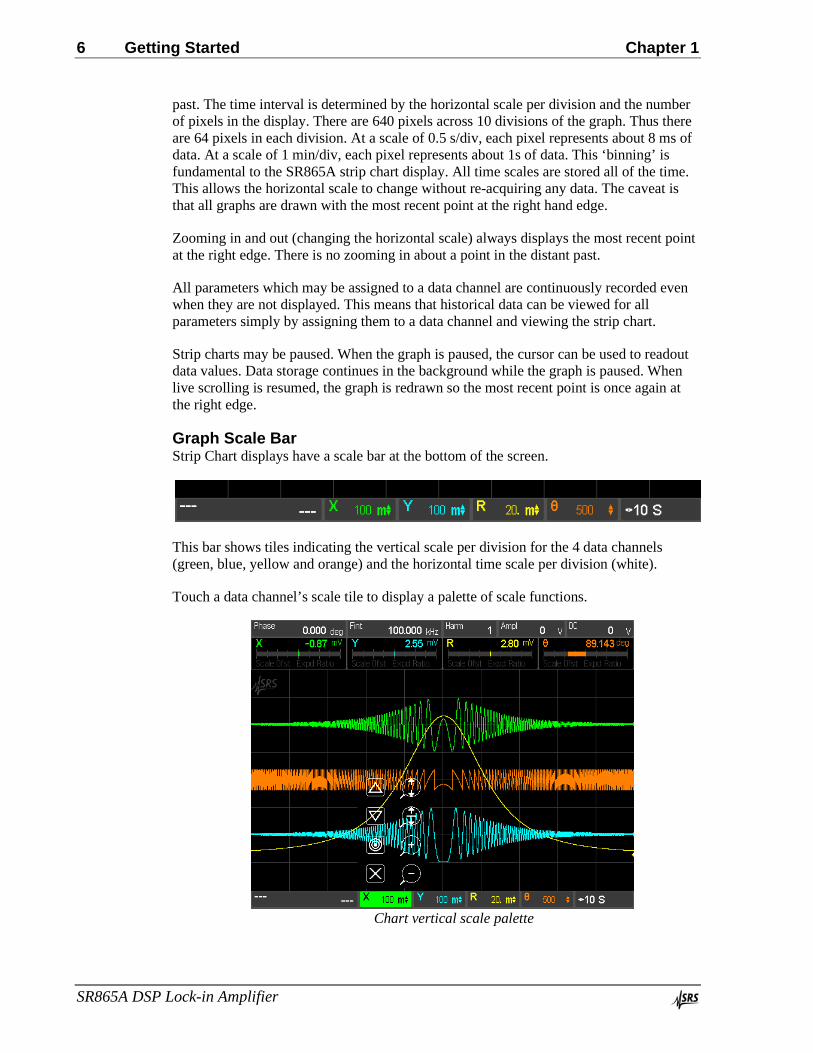
Graph Scale Bar Strip Chart displays have a scale bar at the bottom of the screen.
This bar shows tiles indicating the vertical scale per division for the 4 data channels (green, blue, yellow and orange) and the horizontal time scale per division (white).
Touch a data channel’s scale tile to display a palette of scale functions.
Chart vertical scale palette

Chapter 1 Getting Started 7
SR865A DSP Lock-in Amplifier
Use the palette functions to scale the selected data channel’s graph. Touch the scale tile again to dismiss the palette.
Vertical Scale Palette Horizontal Scale Palette
Vertical Scale Palette Vertical scale changes are applied to each data channel separately. Autoscale adjusts the scale and center so the graph occupies as much of the screen as possible. Autoscale Zero Center forces the center of the graph to be zero and then sets the scale to show the data. The location of zero is indicated by the small triangle on the right edge. It points left where zero is. It points up or down if zero is above or below the graph.
Zoom In and Zoom Out change the scale about the center. Use Center Newest Point to bring the current point to the center of the graph before zooming in or out. Move Up and Move Down simply move the graph up and down on the screen. The graph can also be moved simply by touching and dragging on the screen while the vertical scale palette is displayed.
Each graph can also be turned off. Touch the scale tile to turn the graph back on.
All changes to the graphs are non-destructive. They simply change the way data is visualized. Stored parameter values are not altered by scale changes.
Horizontal Scale Palette Horizontal scale changes are applied to the entire strip chart display and all data channels.
Zoom In and Zoom Out change the horizontal scale and scroll speed.
Pause stops the chart scrolling and pauses the graph. When the graph is paused, the cursor can be used to readout data values. These readouts correspond to the min, max or mean of the data in the time bin at the cursor location. The time of the cursor location is displayed in the tile at the left edge of the scale bar below the graph. Touch this tile to switch between elapsed time from the right edge to absolute time (time and date when the point was taken). Use Cursor MinMaxMean and Cursor Width to change the cursor. Note that the cursor marker may not lie on the data graph for wide cursors since the marker shows the min, max or mean of all the data within the cursor width.

8 Getting Started Chapter 1
SR865A DSP Lock-in Amplifier
The cursor is only displayed when the graph is paused.
Zooming in and out preserves the right hand edge of the graph at the point in time when the graph was paused.
Data storage continues in the background while the graph is paused. When live scrolling is resumed with Resume, the graph is redrawn so the current point is once again at the right edge.

Chapter 1 Getting Started 9
SR865A DSP Lock-in Amplifier
The Basic Lock-in This measurement is designed to use the internal oscillator to explore some of the basic lock-in functions. Specifically, you will measure the amplitude of the Sine Out at various frequencies, amplitudes, time constants and phase shifts.
Do This Explanation
1. Disconnect all cables from the lock-in. Turn the power on while holding down the [Local] key. The power switch is on the power entry module on the rear panel.
When the power is turned on with [Local] pressed, the lock-in returns to its standard default settings. See the Standard Settings list in the Operation section for a complete listing of the settings.
2. Connect the Sine Out + on the front panel to the A input using a BNC cable.
The lock-in defaults to the internal oscillator reference set at 100.000 kHz. The reference source is indicated by the Internal LED. In this mode, the lock-in generates a synchronous sine output at the internal reference frequency.
The default data screen is the Trend Graph. The 4 displayed parameters default to X, Y, R and θ. Each parameter has a numeric display, a bar graph and a trend graph. The trend graph is a continuously autoscaling graph of the recent history of each parameter. This data screen has no adjustments available.
The default sine amplitude is 0 Vrms. Thus the data displays will read 0 for X, Y and R. θ will be just noise.
3. Touch Ampl in the info bar along the top of the screen. Then 500mV.
The lock-in parameters shown in the info bar at the top of the screen may be entered using a numeric keypad simply by touching them.
The Sine Out amplitude is specified for differential output (Sine+) − (Sine−). In this case, each BNC has an amplitude of 250 mV (rms) with a 50Ω output. The lock-in input is high impedance so the output of each BNC is doubled and the lock-in measures 500 mV.
Since the phase shift of the sine output is very close to zero, X (green) should read about 0.5000 and Y (blue) should read close to 0.0000 V.
4. Press the [Auto Phase] key. Automatically adjust the reference phase shift to eliminate any residual phase error. This should set the values of Y and θ to zero.

10 Getting Started Chapter 1
SR865A DSP Lock-in Amplifier
5. Press the [+90º] key. This adds 90º to the reference phase shift. The value of X drops to zero and Y becomes minus the magnitude (−0.5000 V).
Use the <Phase> knob to adjust the phase shift back to zero (press and hold the <Phase> knob inward as a short cut). The Phase shift is displayed in the info bar at the top of the screen.
The lock-in parameters shown in the info bar, Phase, Reference Frequency, Detected Harmonic, Sine Amplitude and Offset, can all be adjusted from the front panel as well as via a touchscreen keypad.
6. Touch Fint in the info bar.
Display the numeric entry screen for internal reference frequency. The 4 buttons labelled F1 thru F4 are frequency presets. Press and hold them to memorize new frequencies.
Touch 10kHz to enter a new frequency. Change the frequency to 10 kHz.
Use the <Frequency> knob to adjust the frequency to 1.00000 kHz.
The knob is very useful for making small adjustments or optimizing a setting. Large changes are better left to the numeric keypad.
The measured signal amplitude X and R should stay within 1% of 500 mV and Y and θ should stay close to zero.
7. Use the <Amplitude> knob to adjust the sine out to 5.0 mV. The Amplitude is displayed in the info bar.
As the amplitude is changed, the values of X and R change to follow.
The yellow LED in the Input Range section should light. The Input Range is the largest input signal before overload. The lower the range, the higher the gain. The signal strength indicates how much of the A/D converter range is being used. When the yellow indicator lights, it means that more gain should be used.
Since the signal has just been reduced by a factor of 100, the input range should be adjusted as well.
8. Press [Auto Range]. The Auto Range function changes the Input Range to maximize the signal at the A/D

Chapter 1 Getting Started 11
SR865A DSP Lock-in Amplifier
converter without overload. In this case the Input Range should change to 10 mV.
The Input Range is the peak allowable voltage at the input, whether noise or signal. In this case, the signal is 5 mVrms or 7 mVpk so 10 mV is the best allowed setting.
The signal strength increases from the minimum (yellow) to something in the middle.
9. Use the <Amplitude> knob to increase the sine out to 50.0 mV. The Amplitude is displayed in the info bar.
The peak signal exceeds the input range so the Input Range Overload LED lights. Ovld indicators also appear on the screen when a displayed value has an input overload.
10. Press [Auto Range]. During Input Range Overload, the Auto Range function selects the 1 V range.
Press [Auto Range] again. From the 1 V range, the Auto Range function changes the Input Range to maximize the signal at the A/D converter without overload. The Input Range should change to 100 mV.
11. Press [Input Range Down] to select 30 mV. Settings which have many options, such as Input Range, Time Constant and Sensitivity, are changed with up and down keys. The setting is indicated by LEDs.
The peak signal exceeds the input range so the Input Range Overload LED lights. Ovld indicators also appear on the screen when a displayed value has an input overload.
Press [Input Range Up] to select 100 mV.
12. Press [Sensitivity Down] multiple times to select 50 mV.
The Sensitivity is indicated with 3 LEDs. In this case, the 5, ×10 and mV should be lit.
The Sensitivity sets full scale for the bar graphs and the resolution for the numeric readouts for X, Y and R. Sensitivity is also the signal reading corresponding to 10 V on the CH1 and CH2 outputs (for X, Y and R).
By decreasing the scale value, the bar graphs and numeric readings display much more resolution for the smaller signal.
13. Press [Time Constant Down] multiple times to select 300 μs.
The Time Constant is indicated with 3 LEDs. In this case, the 3, ×100 and μs.

12 Getting Started Chapter 1
SR865A DSP Lock-in Amplifier
The output values become noisy. This is because the 2f component of the output (at 2 kHz) is no longer attenuated completely by the low pass filter.
The red Output Overload LED for CH1 will light indicating that the output voltage is clipping. The 50 mV signal outputs 10 V when the sensitivity is 50 mV. The large additional 2f component will cause the output to try and exceed 10 V and results in an output overload. Output overload does not affect the actual displayed value, it just indicates that the CH1 (or CH2) output is not following the measured value.
14. Press [Slope] to select 12 dB/oct. Parameters which have only a few values, such as Filter Slope and External Source, have only a single key which cycles through all available options. Press the key until the desired option is indicated by an LED.
The outputs are less noisy with 2 poles of filtering.
Press [Slope] twice more to select 24 dB/oct. With 4 poles of low pass filtering, even this short time constant attenuates the 2f component reasonably well and provides steady readings.
Press [Slope] again to select 6 dB/oct. Let's leave the filtering short and the outputs noisy for now.
15. Press [Sync] to turn on synchronous filtering. This turns on synchronous filtering whenever the detection frequency is below 4.8 kHz.
Synchronous filtering effectively removes output components at multiples of the detection frequency. At low frequencies, this filter is a very effective way to remove 2f without using extremely long time constants.
The outputs are now quiet and steady, even though the time constant is very short. The response time of the synchronous filter is equal to the period of the detection frequency (1 ms in this case).
This concludes this measurement example. You should have a feeling for the basic operation of the front panel. Basic lock-in parameters have been introduced and you should be able to perform simple measurements.

Chapter 1 Getting Started 13
SR865A DSP Lock-in Amplifier
Using Displays This measurement is designed to use the internal oscillator and an external signal source to explore some of the display types. You will need a synthesized function generator capable of providing a 500 mVrms sine wave at 100.000 kHz, BNC cables and a terminator appropriate for the generator function output.
Specifically, you will display the lock-in outputs when measuring a signal close to, but not equal to, the internal reference frequency. This setup ensures changing outputs which are more illustrative than steady outputs.
Do This Explanation
1. Disconnect all cables from the lock-in. Turn the power on while holding down the [Local] key. The power switch is on the power entry module on the rear panel.
When the power is turned on with [Local] pressed, the lock-in returns to its standard default settings. See the Standard Settings list in the Operation section for a complete listing of the settings.
2. Turn on the function generator, set the frequency to 100.000 kHz (exactly) and the amplitude to 500 mVrms.
Connect the function output (sine wave) from the synthesized function generator to the A input using a BNC cable and appropriate terminator.
The input impedance of the lock-in is 10 MΩ. The generator may require a terminator. Many generators have either a 50Ω or 600Ω output impedance. Use the appropriate feedthrough or T termination if necessary. In general, not using a terminator means that the function output amplitude will not agree with the generator setting.
The default screen is the Trend Graph. Four data channels are displayed as values, bar and trend graphs. The trend graph is the recent history of each data channel with continuous auto-scaling. In this case R (yellow) auto scales to show the tiny amount of noise in the signal magnitude. Trend graphs have no adjustments and are most useful when adjusting an experiment to find a maximum or minimum.
The lock-in defaults to the internal oscillator reference set at 100.000 kHz. The reference source is indicated by the Internal LED.
The internal oscillator should be very close to the actual generator frequency. The X (green) and Y (blue) displays should read values which change slowly. The lock-in and the generator are not phase locked but they are at (nearly) the same frequency with a slowly changing θ (orange). The signal magnitude R (yellow) is phase independent and does not change.

14 Getting Started Chapter 1
SR865A DSP Lock-in Amplifier
3. Use the <Frequency> knob to carefully adjust the frequency to 99.9998 kHz. That’s 0.2 Hz below 100 kHz.
By setting the lock-in reference 0.2 Hz away from the signal frequency, the X and Y outputs are 0.2 Hz sine waves (difference between fref and fsig). The X and Y displays should now oscillate at about 0.2 Hz (the accuracy is determined by the timebases of the generator and the lock-in).
4. Press [Screen Layout] once to change the display to the full screen strip chart.
The most common way to visualize the lock-in outputs is to use the strip chart display. New data is plotted at the right edge and older data scrolls left. The scroll rate is determined by the horizontal scale (time per division). The fastest rate is 0.5 s/div and the shows 5 s of history.
The info bar is at the top of the screen. Touch a tile to change a parameter using a keypad.
The numeric and bar graph displays shrink to fit above the chart.
The scale bar is shown below the strip chart. This bar shows tiles indicating the vertical scale per division for the 4 data channels (green, blue, yellow and orange) and the horizontal time scale per division (white).
5. Touch the orange scale tile θ at the bottom to display the vertical scale palette.
Use the palette functions to adjust the vertical scale of the selected data channel’s trace. Touch the scale tile again to dismiss the palette.
The trace may be moved up and down, auto scaled, zoomed in and out and dismissed entirely.

Chapter 1 Getting Started 15
SR865A DSP Lock-in Amplifier
Touch to auto scale the orange θ graph.
Touch to auto scale a trace. Touch to auto scale while keeping zero in the center.
The phase is ramping from −180º to +180º so the resulting scale is 50/div for a graph of ±200º.
Touch the orange scale tile again to dismiss the scale palette.
6. Touch the green scale tile X to display its scale palette.
Touch to auto scale the green X trace.
Selecting a scale tile automatically dismisses any other palette.
Touch a highlighted scale tile to simply dismiss its palette leaving all palettes off.
7. Touch the blue scale tile Y to display its scale palette.
Touch to auto scale the blue Y trace.
The X and Y outputs are 0.2 Hz sine waves with 500 mV amplitudes.
8. Touch the yellow scale tile R to display its scale palette.
Touch to move the trace so the newest points are vertically centered.
Touch repeatedly to zoom in about the center. Keep zooming in until the yellow trace shows some noise. The scale will probably end up less than 1 mV.
The magnitude R is phase independent and is a straight flat line at about 500 mV.
By centering the trace, the zoom function will expand the trace to reveal noise on R.
The little triangles along the right edge indicate the zero for each data channel. Zooming in on R moves the zero for R below the graph as indicated by the downward facing yellow triangle at the bottom right edge.

16 Getting Started Chapter 1
SR865A DSP Lock-in Amplifier
9. Touch and drag in the graph area while the yellow scale palette is displayed to move the yellow trace up and down.
When a trace is selected (by displaying its scale palette) touching anywhere inside the graph area (and not a scale button) drags the trace up and down.
The and buttons also move the trace up and down.
10. Touch the highlighted yellow scale tile R to dismiss its scale palette.
Now touch anywhere within the graph area.
Touching within the graph area when no trace is selected turns on a status display across the top of the graph. This displays the lock-in signal settings.
This status is useful when the HDMI port (on the rear panel) is used to drive an external monitor or TV. Users who are looking at the monitor can see the lock-in front panel settings.
Touch anywhere within the graph area to dismiss the status display.
The status display is dismissed when the graph area is touched or a scale palette is displayed. Simply turn it back on with a touch if desired.
11. Touch the white scale tile Time to display the horizontal scale palette.
Touch repeatedly to zoom out.
Horizontal scale changes are applied to the entire strip chart display and all data channels.
Zooming changes the horizontal scale and scroll speed. The chart always displays the most recent point at the right edge.
In this case, zooming out displays more history and more cycles of X, Y and θ appear.
12. Increase the amplitude of the function generator to 1.5 Vrms.
The signal now exceeds the input range of 1 V (peak) so the Input Range Overload LED is on. ‘Ovld’ indicators are displayed for X, Y, R and

Chapter 1 Getting Started 17
SR865A DSP Lock-in Amplifier
θ because these values are affected by signal overload.
Conditions such as overload or reference unlock are displayed in violet along the bottom. This provides visual feedback about the validity of the data in those regions.
Decrease the amplitude of the function generator back to 500 mVrms.
The overload condition goes away.
13. Touch the white scale tile Time to display the horizontal scale palette.
Touch repeatedly to zoom out.
Touch repeatedly to zoom back in.
Zoom out on the horizontal time scale to show more and more history. When the region where the signal was overloaded is shown, the overload is indicated by the violet points along the bottom edge.
14. Press [Screen Layout] once to change the display to the half screen strip chart.
The half screen strip chart behaves the same as the full screen version. The only difference is that the numeric and bar graphs are full sized.

18 Getting Started Chapter 1
SR865A DSP Lock-in Amplifier
15. Press [Screen Layout] again to change the display to the full screen FFT.
The FFT of the signal input is displayed. There is only a single quantity shown.
The left and right edge frequencies are labelled at the bottom of the graph. The cursor readout is at the right.
The display is adjusted with the tiles across the bottom. Src selects the source data for the FFT. dB and Hz adjust the vertical and horizontal scales. Avgs sets the amount of averages and Live toggles to Paused.
Use the <Cursor> knob to move the cursor.
16. Press [Screen Layout] again to change the display to the half screen FFT.
The half screen FFT display behaves the same as the full screen version. The only difference is that the numeric and bar graphs are full sized.
17. Press [Screen Layout] again to change the display to the full numeric display.
The full numeric screen adds readouts and bar graphs for the 4 aux inputs on the rear panel. The 4 aux outputs are shown in tiles across the bottom. Touching an output tile displays a keypad to set the aux output.

Chapter 1 Getting Started 19
SR865A DSP Lock-in Amplifier
18. Press [Screen Layout] again to cycle back to the trend graph.
Use [Screen Layout] to cycle through the various display screens.
This concludes the measurement example. You should have a feeling for the basic operation of the display screens.

20 Getting Started Chapter 1
SR865A DSP Lock-in Amplifier
Sensitivity, Offset and Expand This measurement is designed to use the internal oscillator to explore some of the basic lock-in outputs. You will need BNC cables and a digital voltmeter (DVM).
Specifically, you will measure the amplitude of the Sine Out and provide analog outputs proportional to the measurement. The effect of offsets and expands on the displayed values and the analog outputs will be explored.
Do This Explanation
1. Disconnect all cables from the lock-in. Turn the power on while holding down the [Local] key. The power switch is on the power entry module on the rear panel.
When the power is turned on with [Local] pressed, the lock-in returns to its standard default settings. See the Standard Settings list in the Operation section for a complete listing of the settings.
2. Connect the Sine Out + on the front panel to the A input using a BNC cable.
The lock-in defaults to the internal oscillator reference set at 100.000 kHz.
The default data screen is the Trend Graph. The 4 displayed parameters default to X, Y, R and θ. Each parameter has a numeric display, a bar graph and a trend graph. The trend graph is a continuously autoscaling graph of the recent history of each parameter. This data screen has no adjustments available.
The default sine amplitude is 0 Vrms. Thus the data displays will read 0 for X, Y and R. θ will be just noise.
3. Touch Ampl in the info bar along the top of the screen. Then 100mV.
The lock-in parameters shown in the info bar at the top of the screen may be entered using a numeric keypad simply by touching them.
The Sine Out amplitude is specified for differential output (Sine+) − (Sine−). In this case, each BNC has an amplitude of 50 mV (rms) with a 50Ω output. The lock-in input is high impedance so the output of each BNC is doubled and the lock-in measures 100 mV.
Since the phase shift of the sine output is very close to zero, X (green) should read about 0.1000 and Y (blue) should read close to 0.0000 V.

Chapter 1 Getting Started 21
SR865A DSP Lock-in Amplifier
4. Connect the CH1 Output on the front panel to the DVM. Set the DVM to read dc Volts.
The CH1 output defaults to X. The output voltage (with ratio disabled) is given by:
10VExpandOffsetySensitivit
XCH1 ××
−=
In this case, X = 0.1 V, Sensitivity = 1 V, the offset is zero percent and the expand is 1. The output should thus be 1 V or 10% of full scale.
Note that the bar graph for X (and R) is at +10%. The Sensitivity (1 V) sets the full scale for the bar graphs of X, Y and R.
5. Press [Screen Layout] twice to show the half screen strip chart.
Now let’s look at how the Sensitivity affects the different displays.
6. Touch the green scale tile X to display its scale palette.
Touch to auto scale the green X trace.
Touch the green highlighted scale tile again to dismiss the scale palette.
auto scales the trace keeping zero at the center. The zero location is indicated by the small green triangle on the right edge. The scale is 50 mV/div so the green data is a line 2 divisions above the center.
7. Press [Sensitivity Down] to select 500 mV.
The DVM should now read 2 V. This is because X (100 mV) is now 20% of the sensitivity (500 mV). This also increases the bar graph to +20% and increases the resolution of the numeric readout.

22 Getting Started Chapter 1
SR865A DSP Lock-in Amplifier
Note that the trace of X is unchanged. This is because the value of X is unchanged.
The Sensitivity does not affect the value of the output, just the way the value is scaled to the displays and analog output.
The Sensitivity applies to X, Y and R.
8. Press [Sensitivity Down] two more times to select 100 mV.
The DVM should now read 10 V and X is now 100% of full scale on the bar graph.
It is important to adjust the Sensitivity even if the analog outputs are not being used. The Sensitivity determines the resolution of the numeric readouts and bar graphs.
[Auto Scale] will adjust the Sensitivity automatically.
9. Press and hold the <CH1 Offset> knob (above the CH1 BNC) to display the offset keypad.
X, Y and R may all be offset, ratioed, and expanded separately.
Since CH1 is set to X (indicated by the X LED above the [Select] key) the <CH1 Offset> knob and [Expand] key above the CH1 BNC set the X offset and expand.
The [CH1 Select] key determines which quantity (X or R) is offset, ratioed, or expanded, and output on the BNC.
The ratio function is described later in this manual, in the Operation chapter. Here we will explore offset and expand.
10. Touch Auto in the offset keypad screen. Auto Offset automatically adjusts the X offset (or Y or R) such that X (or Y or R) becomes zero. In this case, X is offset to zero. The offset should be about 100%. Offsets are set as a

Chapter 1 Getting Started 23
SR865A DSP Lock-in Amplifier
percentage of the Sensitivity up to 999% (10×). Offsets are useful for making relative measurements.
Offsets can also be set using the keypad or <Offset> knob.
The offset affects the value of X and any outputs or displays of X. The DVM voltage should be zero in this case.
The Offset indicator turns on next to the <CH1 Offset> knob. The X display on the screen has an ‘Ofst’ indication that the displayed quantity is affected by an offset. In this case, the bar graph and numeric value are both zero.
11. Touch 90Enter to set the offset to 90%. The X output (10 mV) is now 10% of the sensitivity (100 mV). The bar graph is at 10% and the DVM reads 1 V.
Notice that the trace of X (green) is a line 10 mV above zero (center). This is because the offset affects the value of X (unlike the sensitivity).
12. Press the <CH1 Offset> knob briefly once to turn the X offset off.
The offset for CH1 can be turned on and off without changing the offset value. Notice how the trace of X changes when the offset is turned off.
Press it again to turn it back on. Leave the X offset on for now.
13. Press [CH1 Expand] once to select ×10. Expand ×10 effectively decreases the sensitivity by 10 after the offset is applied.
10VExpandOffsetySensitivit
XCH1 ××
−=
Now, X = 100 mV, Sensitivity = 100 mV, the offset is 90% and the expand is ×10. Thus the DVM reads 10 V.
The X bar graph is now at 100% and the numeric readout has added resolution. The X display has an ‘Expd’ indication that the displayed quantity is affected by a non-unity expand.
Expand increases the resolution of the X display and CH1 output. Note that the trace of X is unaffected by expand. This is because expand does not change the value of X.

24 Getting Started Chapter 1
SR865A DSP Lock-in Amplifier
14. Press [CH1 Expand] once to select ×100. The red output Overload LED lights and a ‘Scale’ overload is indicated in the X display. This is because CH1 is trying to reach 100 V (10 times the previous DVM reading). Since the CH1 output is limited to 10 V, the output is overloaded. This has no affect on the value of X and the trace is unchanged. The bar graph and displayed value are pinned however.
15. Press [CH1 Expand] once to turn off expand.
Press the <CH1 Offset> knob briefly once to turn the X offset off.
The X display returns to 100 mV, 100% bar graph and 10 V CH1 output. The X graph is a line at 100 mV 2 divisions above center.
With offset and expand, the output voltage gain and offset can be programmed to provide control of feedback signals with the proper bias and gain for a variety of situations.
Offsets add and subtract from the values of X, Y and R.
Expand increases the resolution of the displays and analog outputs but does not change the values of X, Y and R.
16. Touch the green scale tile X to display its scale palette.
Touch to auto scale the green X trace.
When using the strip chart graph exclusively, there is no need to use offset or expand to zoom in on the data. Simply auto scale the data channel to graphically offset and expand the chart data.
See the Outputs and Scales discussion in the next chapter for more detailed information on output scaling

Chapter 1 Getting Started 25
SR865A DSP Lock-in Amplifier
Saving and Recalling Setups The SR865A can store 8 complete instrument setups in non-volatile memory.
Do This Explanation
1. Disconnect all cables from the lock-in. Turn the power on while holding down the [Local] key. The power switch is on the power entry module on the rear panel.
When the power is turned on with [Local] pressed, the lock-in returns to its standard default settings. See the Standard Settings list in the Operation section for a complete listing of the settings.
2. Press and hold [Calc/system] to display the system menu.
First let’s set the SR865A clock.
The system menu is where instrument parameters (not measurement parameters) are set. This includes file numbering, interface settings and software updates.
3. Touch the h button in the Time section to highlight the hours setting. Use the keypad to set the hour of day in 24 hour format. The time/date will highlight in orange indicating that the displayed time is not the current time but rather the time to be set.
Continue to enter the minutes, seconds then touch Time set to commit the time to the internal clock.
Set the date in the same manner touching Date set] to commit the date.
The time and date are used to label data files, screen shots, and saved settings.
4. Press [Sensitivity Down] 3 times to select 100 mV.
Press [Time Constant Up] twice to select 1 s.
Let’s change the lock-in setup so that we have a non-default setup to save.
Change the Sensitivity, Time Constant and Filter Slope.

26 Getting Started Chapter 1
SR865A DSP Lock-in Amplifier
Press [Filter Slope] once to select 12 dB/oct.
5. Press [Save Recall] to display the Save/Recall screen.
The SR865A can store 8 complete setups. In addition the default setup can be recalled.
6. Touch the Save button next to the large tile labelled ‘1’.
Enter a name for this setup using the keypad.
Touch Confirm to commit the current setup to location 1.
Setups are numbered 1 through 8. Setups should be named so they are easily distinguished.
7. Now change the Sensitivity, Time Constant and Filter Slope to new settings.
Change the lock-in setup before recalling the saved settings.
8. Press [Save Recall] to display the Save/Recall screen again.
Note that the Location 1 tile displays the setup name and the time and date it was created. This makes it easier to recall the correct setup.

Chapter 1 Getting Started 27
SR865A DSP Lock-in Amplifier
9. Touch Recall for Location 1.
A summary of settings which will change upon recall is shown.
Simply touch Cancel to skip recalling this setup.
Touch Confirm to recall the setup and dismiss this screen.
The Sensitivity, Time Constant and Filter Slope should all return to the saved settings.

28 Getting Started Chapter 1
SR865A DSP Lock-in Amplifier
Aux Outputs and Inputs This measurement is designed to illustrate the use of the Aux Outputs and Inputs on the rear panel. You will need BNC cables and a digital voltmeter (DVM).
Specifically, you will set the Aux Output voltages and measure them with the DVM. These outputs will then be connected to the Aux Inputs to simulate external dc voltages which the lock-in can measure.
Do This Explanation
1. Disconnect all cables from the lock-in. Turn the power on while holding down the [Local] key. The power switch is on the power entry module on the rear panel.
When the power is turned on with [Local] pressed, the lock-in returns to its standard default settings. See the Standard Settings list in the Operation section for a complete listing of the settings.
2. Connect Aux Out 1 on the rear panel to the DVM. Set the DVM to read dc volts.
The 4 Aux Outputs can provide programmable voltages between −10.5 and +10.5 volts. The outputs can be set from the front panel or via the computer interface.
3. Press [Aux Output] to show the Aux Output keypad.
Aux Outputs are easily set from the front panel.
4. Touch 10Enter to set Aux 1 to 10.000 V. The DVM should display 10.00 V.
Use the <Cursor> knob adjust the level to 5.000 V.
The <Cursor> knob is used to adjust values when the Aux Output keypad is shown.
The DVM should display 5.00 V.
The 4 Aux Outputs are useful for controlling other parameters in an experiment, such as pressure, temperature, wavelength, etc.

Chapter 1 Getting Started 29
SR865A DSP Lock-in Amplifier
5. Touch [Screen Layout] multiple times to show the full numeric display screen.
Note the 4 Aux Output values are displayed in white tiles across the bottom. Touching an output tile will display the Aux Output keypad.
This screen displays the 4 Aux Input readings along with the 4 lock-in data channels. The Aux Inputs are always scaled to 10 V.
The Aux Inputs can read 4 analog voltages. These inputs are useful for monitoring and measuring other parameters in an experiment, such as pressure, temperature, position, etc.
6. Disconnect the DVM from Aux Out 1. Connect Aux Out 1 to Aux In 1 on the rear panel.
We'll use Aux Out 1 to provide an analog voltage to measure.
Aux In 1 should now read 5.000 V.
The Aux Inputs can be assigned to a data channel and graphed on the strip chart alongside lock-in outputs. Use the [Config] key to change a data channel.

30 Getting Started Chapter 1
SR865A DSP Lock-in Amplifier
Scanning This measurement is designed to use the internal oscillator and an external signal source to explore some of the display types. You will need a synthesized function generator capable of providing a 500 mVrms sine wave at 100.000 kHz, BNC cables and a terminator appropriate for the generator function output.
Specifically, you will scan the lock-in internal reference frequency through the signal frequency.
Do This Explanation
1. Disconnect all cables from the lock-in. Turn the power on while holding down the [Local] key. The power switch is on the power entry module on the rear panel.
When the power is turned on with [Local] pressed, the lock-in returns to its standard default settings. See the Standard Settings list in the Operation section for a complete listing of the settings.
2. Turn on the function generator, set the frequency to 100.000 kHz (exactly) and the amplitude to 500 mVrms.
Connect the function output (sine wave) from the synthesized function generator to the A input using a BNC cable and appropriate terminator.
The input impedance of the lock-in is 10 MΩ. The generator may require a terminator. Many generators have either a 50Ω or 600Ω output impedance. Use the appropriate feedthrough or T termination if necessary. In general, not using a terminator means that the function output amplitude will not agree with the generator setting.
The internal oscillator should be very close to the actual generator frequency. The X (green) and Y (blue) displays should read values which change slowly. The lock-in and the generator are not phase locked but they are at the same frequency with some slowly changing θ (orange). The signal magnitude R (yellow) is phase independent and does not change.
3. Press and hold [Scan/setup] to display the scan menu.
Parameters which may be scanned are Finternal, Amplitude, DC Level, Aux Out 1 and 2.
Scans can be linear or logarithmic, repeat, repeat up and down or run once and pause.
The Scan Duration is the total time to move from the Begin Value to the End Value. The Parameter Update Interval is the time spent at each scan step along the way. The shorter the update time, the smaller the steps and the smoother the scan. The longer the update time, the fewer steps. With experiments that take time to settle after a parameter change, it can be beneficial to set the update time long enough to accommodate the settling.

Chapter 1 Getting Started 31
SR865A DSP Lock-in Amplifier
4. Let’s leave the Scan Parameter at internal reference frequency.
Touch Begin Value to highlight the start frequency. Enter 99.990 kHz.
Touch End Value to highlight the stop frequency. Enter 100.010 kHz.
Let’s scan a 20 Hz span around the signal frequency (100.000 kHz).
This setup will increase the internal frequency from 99.990 kHz to 100.010 kHz. To reverse the scan, simply reverse the begin and end values.
5. Touch End Mode once to select Repeat. This will repeat the scan over and over jumping from the end value back to the begin value at the end of each scan.
6. Touch Close to return to the Trend Graphs. The lock-in frequency has not been changed, we have only configured a scan. The scan has not been started.
7. Press [Scan/setup] briefly (don’t hold it) to turn on the scan.
The Ready LED turns on indicating that the scan is ready (at the start value). In this case, the internal frequency (in the info bar at the top) is shown in orange indicating that it is under scan control. At this time, the frequency is the start value or 99.9900 kHz.
8. Press [Play Pause/reset] briefly (don’t hold it) to start the scan.
The Run LED turns on indicating that the scan is running.
The internal frequency starts scanning up. The current value is shown in orange in the info bar. When the end value is reached, the scan resets to the beginning value and repeats.
The trend graphs show a resonance as the internal frequency passes through 100.000 kHz. This is because the difference between the fsignal and finternal gets slower as the finternal approaches fsignal and then gets faster after it passes fsignal. The time constant attenuates this difference frequency when it is large.
9. Press [Screen Layout] once to show the full screen strip chart.
Touch the white scale tile Time to display the horizontal scale palette (bottom right of screen).
Touch repeatedly to zoom out to 10 S/div.
It is much easier to visualize a scan using the strip charts since the chart time scale can be matched to the scan time.
This scan takes 1m40s or 100 s so a chart span of 100 s will display an entire scan.

32 Getting Started Chapter 1
SR865A DSP Lock-in Amplifier
10. Touch the green scale tile X to display its scale palette. Touch to dismiss the X trace.
Touch the blue scale tile Y to display its scale palette. Touch to dismiss the Y trace.
Let’s clean up the chart by dismissing the X and Y traces.
11. Touch the yellow scale tile R to display its
scale palette. Touch to auto scale the R trace.
Touch the orange scale tile θ to display its scale palette. Touch to repeatedly to change the scale to 200 deg/div.
The magnitude trace (R) shows the lock-in response as the internal frequency scans through the signal frequency at this time constant and filter.
Reduce the phase trace to see the resonance at 100.000 kHz.
12. Press [Config] to change the assignments of the data channels.
Touch Data 2 Display (the blue display) to highlight the channel 2 data source. Touch Fint from the keypad below.
Touch Close to return to the strip chart.
It would be nice to show the frequency on the graph.
The 4 data channels can be assigned to different parameters in the Config screen.
Any data channel can be assigned any of the sources in the keypad.
When the Config screen is closed the strip chart does not display a blue trace. This is because we dismissed it previously.

Chapter 1 Getting Started 33
SR865A DSP Lock-in Amplifier
13. Touch the blue scale tile Fi to display its scale palette.
Touch to auto scale the blue F trace.
Simply touching the blue scale tile turns the blue trace back on and displays its scale palette.
The blue frequency trace shows the upward scan of the frequency spanning 4 divisions or 20 Hz.
14. Touch the white scale tile Time to display the horizontal scale palette (bottom right of screen).
Touch repeatedly to zoom out a few times.
Since the scan End Mode is set to repeat, we see the scan repeat over and over in the history.
When scanning, it is convenient to pause the strip chart at the end of the scan to review the results.
15. Press and hold [Scan/setup] to display the scan menu again.
Touch End Mode multiple times to select Once.
Touch Close to return to the strip chart.
When the End Mode is Once, then the scan stops at the end value and the strip chart is paused.
16. Press [Scan/setup] briefly (don’t hold it) to turn the scan off, then press [Scan/setup] briefly again to re-arm.
Changes to the scan setup do not affect a currently-running scan. We stop the scan and then start a new one by cycling the [Scan/setup] button; the Ready LED goes off and then on.

34 Getting Started Chapter 1
SR865A DSP Lock-in Amplifier
17. Press [Play Pause/reset] briefly (don’t hold it) to re-start the scan.
The Run LED turns on indicating that the scan is running.
18. Touch the white scale tile Time to display the horizontal scale palette (bottom right of screen).
Touch repeatedly to zoom in to 10 S/div.
Touch the highlighted white scale tile again to dismiss the scale palette.
This scan is 100 s in length so set the graph to 10 divisions of 10 s to show a complete scan.
Wait for the scan to finish. When the scan finishes, the Done LED turns on.
19. Use the <Cursor> knob to move the cursor to the peak of R (yellow).
When the scan in progress reaches the end value the strip chart pauses.
The frequency will hold at the end value (100.010 kHz) as displayed in the info bar.
The cursor is active when the strip chart is paused.
20. Touch the white scale tile Time to display the horizontal scale palette (bottom right of screen).
Touch start the strip chart again.
Touch the highlighted white scale tile again to dismiss the scale palette.
Notice that data collection continued while the chart was paused. Restarting the chart realigns the time history so the current time is the right edge again.
In this case, the frequency has been constant at 100.010 kHz the entire time we have been examining the paused scan.
21. Press and hold [Play Pause/reset] to reset the scan back to the begin value.
This resets the scan parameter back to the begin value. The Done LED turns off.
22. Press [Play Pause/reset] briefly to start the scan again.
This starts the scan again. The Run LED turns on and the frequency ramps upward.

Chapter 1 Getting Started 35
SR865A DSP Lock-in Amplifier
While the scan is in progress, press [Scan/setup] briefly to turn scanning off.
Turn the scan off before the end and the internal frequency returns to its original value (100.000 kHz) as shown in white in the info bar.

36 Getting Started Chapter 1
SR865A DSP Lock-in Amplifier

Basics 37
SR865A DSP Lock-in Amplifier
Chapter 2 Lock-in Amplifier Basics
What is a Lock-in Amplifier? Lock-in amplifiers are used to detect and measure very small ac signals — all the way down to a few nanovolts. Accurate measurements may be made even when the small signal is obscured by noise sources many thousands of times larger.
Lock-in amplifiers use a technique known as phase-sensitive detection to single out the component of the signal at a specific reference frequency and phase. Noise signals at frequencies other than the reference frequency are rejected and do not affect the measurement.
Why use a lock-in? Let's consider an example. Suppose the signal is a 10 nV sine wave at 10 kHz. Clearly some amplification is required. A good low noise amplifier may have about 5 nV/√Hz of input noise. If the amplifier bandwidth is 100 kHz and the gain is 1000, then we can expect our output to be 10 μV of signal (10 nV × 1000) and 1.6 mV of broadband noise (5 nV/√Hz × √100 kHz × 1000). We won't have much luck measuring the output signal unless we single out the frequency of interest.
If we follow the amplifier with a band pass filter with a Q=100 (a very good filter) centered at 10 kHz, any signal in a 100 Hz bandwidth will be detected (10 kHz/Q). The noise in the filter pass band will be 50 μV (5 nV/√Hz × √100 Hz × 1000) and the signal will still be 10 μV. The output noise is still much greater than the signal and an accurate measurement cannot be made. Further gain will not help the signal to noise problem.
Now try following the amplifier with a phase-sensitive detector (PSD). The PSD can detect the signal at 10 kHz with a bandwidth as narrow as 0.01 Hz! In this case, the noise in the detection bandwidth will be only 0.5 μV (5 nV/√Hz × √.01 Hz × 1000) while the signal is still 10 µV. The signal to noise ratio is now 20 and an accurate measurement of the signal is possible.
What is phase-sensitive detection? Lock-in measurements require a frequency reference. Typically an experiment is excited at a fixed frequency (from an oscillator or function generator) and the lock-in detects the response from the experiment at the reference frequency. In the diagram below, the reference signal is a square wave at frequency fref. This might be the sync output from a function generator. If the sine output from the function generator is used to excite the experiment, the response might be the signal waveform shown below. The signal is Vsigsin(ωref t + θsig) where ωref = 2πfref and Vsig is the signal amplitude.

38 Basics Chapter 2
SR865A DSP Lock-in Amplifier
The SR865A generates its own sine wave at frequency fL, shown as the lock-in reference below. The lock-in reference is sin(ωLt + θref) where ωL = 2πfL.
The SR865A amplifies the signal and then multiplies it by the lock-in reference using a phase-sensitive detector (PSD) or multiplier. The output of the PSD is simply the product of two sine waves.
Vpsd = Vsig sin(ωrt + θsig) sin(ωLt + θref)
= 1/2 Vsig cos([ωr − ωL]t + θsig − θref) −
1/2 Vsig cos([ωr + ωL]t + θsig + θref)
The PSD output is two ac signals, one at the difference frequency (ωr − ωL) and the other at the sum frequency (ωr + ωL).
If the PSD output is passed through a low pass filter, the ac signals are removed. What will be left? In the general case, nothing. However, if ωr equals ωL, the difference frequency component will be a dc signal. In this case, the filtered PSD output will be
Vpsd = 1/2 Vsig cos(θsig − θref)
This is a very nice signal — it is a dc signal proportional to the signal amplitude.
Narrow band detection Now suppose the input is made up of signal plus noise. The PSD and low pass filter only detect signals whose frequencies are very close to the lock-in reference frequency. Noise signals at frequencies far from the reference are attenuated at the PSD output by the low pass filter (neither ωnoise − ωref nor ωnoise + ωref are close to dc). Noise at frequencies very close to the reference frequency will result in very low frequency ac outputs from the PSD (|ωnoise − ωref| is small). Their attenuation depends upon the low pass filter bandwidth and roll-off. A narrower bandwidth will remove noise sources very close to the reference frequency, a wider bandwidth allows these signals to pass. The low pass filter bandwidth determines the bandwidth of detection. Only the signal at the reference frequency will

Chapter 2 Basics 39
SR865A DSP Lock-in Amplifier
result in a true dc output and be unaffected by the low pass filter. This is the signal we want to measure.
Where does the lock-in reference come from? We need to make the lock-in reference the same as the signal frequency, i.e. ωr = ωL. Not only do the frequencies have to be the same, the phase between the signals cannot change with time, otherwise cos(θsig − θref) will change and Vpsd will not be a dc signal. In other words, the lock-in reference needs to be phase-locked to the signal reference.
Lock-in amplifiers use a phase-locked loop (PLL) to generate the reference signal. An external reference signal (in this case, the reference square wave) is provided to the lock-in. The PLL in the lock-in “locks” the internal reference oscillator to this external reference, resulting in a reference sine wave at ωr with a fixed phase shift of θref. Since the PLL actively tracks the external reference, changes in the external reference frequency do not affect the measurement.
All lock-in measurements require a reference signal In this case, the reference is provided by the excitation source (the function generator). This is called an external reference source. In many situations, the lock-in’s internal oscillator may be used instead. The internal oscillator is just like a function generator (with variable sine output and a TTL sync) which is always phase-locked to the reference oscillator.
Magnitude and phase Remember that the PSD output is proportional to Vsigcosθ where θ = (θsig − θref). θ is the phase difference between the signal and the lock-in reference oscillator. By adjusting θref we can make θ equal to zero, in which case we can measure Vsig (cosθ = 1). Conversely, if θ is 90°, there will be no output at all. A lock-in with a single PSD is called a single-phase lock-in and its output is Vsigcosθ.
This phase dependency can be eliminated by adding a second PSD. If the second PSD multiplies the signal with the reference oscillator shifted by 90°, i.e. sin(ωLt + θref + 90°), its low pass filtered output will be
Vpsd2 = 1/2 Vsig sin(θsig − θref)
Vpsd2 ~ Vsig sinθ
Now we have two outputs, one proportional to cosθ and the other proportional to sinθ. If we call the first output X and the second Y,
X = Vsig cosθ Y = Vsig sinθ
these two quantities represent the signal as a vector relative to the lock-in reference oscillator. X is called the 'in-phase' component and Y the 'quadrature' component. This is because when θ = 0, X measures the signal while Y is zero.
By computing the magnitude (R) of the signal vector, the phase dependency is removed.
R = (X2 + Y2)1/2 = Vsig

40 Basics Chapter 2
SR865A DSP Lock-in Amplifier
R measures the signal amplitude and does not depend upon the phase between the signal and lock-in reference.
A dual-phase lock-in, such as the SR865A, has two PSD's, with reference oscillators 90° apart, and can measure X, Y and R directly. In addition, the phase θ between the signal and lock-in reference, can be measured according to
θ = tan−1 (Y/X)
What Does a Lock-in Measure? So what exactly does the SR865A measure? Fourier's theorem basically states that any input signal can be represented as the sum of many sine waves of differing amplitudes, frequencies and phases. This is generally considered as representing the signal in the “frequency domain”. Normal oscilloscopes display the signal in the “time domain”. Except in the case of clean sine waves, the time domain representation does not convey very much information about the various frequencies that make up the signal.
What does the SR865A measure? The SR865A multiplies the input signal by a pure sine wave at the reference frequency. All components of the input signal are multiplied by the reference simultaneously. Mathematically speaking, sine waves of differing frequencies are orthogonal, i.e. the average of the product of two sine waves is zero unless the frequencies are exactly the same. In the SR865A, the product of this multiplication yields a dc output signal proportional to the component of the signal whose frequency is exactly locked to the reference frequency. The low pass filter which follows the multiplier provides the averaging which removes the products of the reference with components at all other frequencies.
The SR865A, because it multiplies the signal with a pure sine wave, measures the single Fourier (sine) component of the signal at the reference frequency. Let's take a look at an example. Suppose the input signal is a simple square wave at frequency f. The square wave is actually composed of many sine waves at multiples of f with carefully related amplitudes and phases. A 2V pk–pk square wave can be expressed as
S(t) = 1.273 sin(ωt) + 0.4244 sin(3ωt) + 0.2546 sin(5ωt) + …
where ω = 2πf. The SR865A, locked to f will single out the first component. The measured signal will be 1.273 sin(ωt), not the 2V pk–pk that you'd measure on a scope.
In the general case, the input consists of signal plus noise. Noise is represented as varying signals at all frequencies. The ideal lock-in only responds to noise at the reference frequency. Noise at other frequencies is removed by the low pass filter following the multiplier. This “bandwidth narrowing” is the primary advantage that a lock-in amplifier provides. Only inputs at the reference frequency result in an output.
RMS or Peak? Lock-in amplifiers as a general rule display the input signal in Volts RMS. When the SR865A displays a magnitude of 1V (rms), the component of the input signal at the reference frequency is a sine wave with an amplitude of 1 Vrms or 2.8 V pk–pk.

Chapter 2 Basics 41
SR865A DSP Lock-in Amplifier
Thus, in the previous example with a 2 V pk–pk square wave input, the SR865A would detect the first sine component, 1.273 sin(ωt). The measured and displayed magnitude would be 0.90 V (rms), e.g. 1.273/√2.
Degrees or Radians? In this discussion, frequencies have been referred to as f (Hz) and ω (2πf radians/sec). This is because people measure frequencies in cycles per second and math works best in radians. For purposes of measurement, frequencies as measured in a lock-in amplifier are in Hz. The equations used to explain the actual calculations are sometimes written using ω to simplify the expressions.
Phase is always reported in degrees. Once again, this is by custom. Equations written as sin(ωt + θ) are written as if θ is in radians mostly for simplicity. Lock-in amplifiers always manipulate and measure phase in degrees.
Block diagram A simplified block diagram of the SR865A’s lock-in circuit is shown below and explained in the following sections.

42 Basics Chapter 2
SR865A DSP Lock-in Amplifier
The Reference Oscillator A lock-in amplifier requires a reference oscillator phase-locked to the signal frequency. In general, this is accomplished by phase-locking an internal oscillator to an externally provided reference signal. This reference signal usually comes from the signal source that is providing the excitation to the experiment.
Reference Input The SR865A reference input can trigger on an analog signal (like a sine wave) or a TTL logic signal. The first case is called External Sine. The input is ac coupled (above 1 Hz) and the input impedance is 1 MΩ. A sine wave input greater than 200 mV pk is required. Positive zero crossings are detected and considered to be the zero for the reference phase shift.
TTL reference signals can be used at all frequencies up to 4 MHz. For frequencies below 1 Hz, a TTL reference signal is required. Many function generators provide a TTL SYNC output which can be used as the reference. This is convenient since the generator's sine output might be smaller than 200 mV or be varied in amplitude. The SYNC signal will provide a stable reference regardless of the sine amplitude.
When using a TTL reference, the reference input trigger can be set to Pos TTL (detect rising edges) or Neg TTL (detect falling edges). In each case, the internal oscillator is locked (at zero phase) to the detected edge.
Internal Oscillator The internal oscillator in the SR865A is basically a 4 MHz function generator with sine and sync outputs. The oscillator generates a digitally synthesized sine wave. The internal oscillator sine wave is output differentially at the SINE OUT BNC’s on the front panel. An attenuator sets the amplitude of the output to a value between 1 nV and 2 V (rms).
When an external reference is used, this internal oscillator sine wave is phase-locked to the reference. The rising zero crossing is locked to the detected reference zero crossing or edge. In this mode, the SINE OUT provides a sine wave phase-locked to the external reference. Phase locking is accomplished digitally by the SR865A.
The internal oscillator may be used without an external reference. In the Internal Reference mode the frequency is set in the lock-in and the SINE OUT provides the excitation for the experiment. The phase-locked-loop is not used in this mode.
The BlazeX output on the rear panel can be configured to provide the sync output. The internal oscillator's rising zero crossings are detected and the output is a square wave.
Reference Oscillators and Phase The internal oscillator sine wave is not the reference signal to the phase sensitive detectors. The SR865A computes a second sine wave, phase shifted by θref from the internal oscillator (and thus from an external reference), as the reference input to the X phase sensitive detector. This waveform is sin(ωrt + θref). The reference phase shift is adjustable in 0.001° increments.

Chapter 2 Basics 43
SR865A DSP Lock-in Amplifier
The input to the Y PSD is a third sine wave, computed by the SR865A, shifted by 90° from the second sine wave. This waveform is sin(ωrt + θref + 90°).
The phase shifts (θref and the 90° shift) are exact numbers and accurate to better than 0.000001°. Neither waveform is actually output in analog form since the phase sensitive detectors are actually digital multipliers inside the SR865A.
Phase Jitter When an external reference is used, the phase-locked loop contributes a little phase jitter. The internal oscillator is supposed to be locked with zero phase shift relative to the external reference. Phase jitter means that the average phase shift is zero but the instantaneous phase shift has a few microdegrees or millidegrees of noise. This shows up at the output as noise in phase or quadrature measurements.
Phase noise can also cause noise to appear at the X and Y outputs. This is because a reference oscillator with a lot of phase noise is the same as a reference whose frequency spectrum is spread out. That is, the reference is not a single frequency, but a distribution of frequencies about the true reference frequency. These spurious frequencies are attenuated quite a bit but can still cause problems. The spurious reference frequencies result in signals close to the reference being detected. Noise at nearby frequencies now appears near dc and affects the lock-in output.
Phase noise in the SR865A is very low and generally causes no problems. In applications requiring no phase jitter, the internal reference mode should be used. Since there is no PLL, the internal oscillator and the reference sine waves are directly linked and there is no jitter in the measured phase. (Actually, the phase jitter is the phase noise of a crystal oscillator and is very, very small).
Harmonic Detection It is possible to compute the two PSD reference sine waves at a multiple of the internal oscillator frequency. In this case, the lock-in detects signals at N× fref which are synchronous with the reference. The SINE OUT frequency is not affected. The SR865A can detect at any harmonic up to N=99 as long as N × fref does not exceed 4 MHz.
The Phase Sensitive Detectors The amplified input signal is converted to digital form using A/D converter sampling at 10 MHz. The SR865A then multiplies the signal with the reference sine wave digitally.
The dynamic reserve is limited by the quality of the A/D conversion. Once the input signal is digitized, no further errors are introduced. Certainly the accuracy of the multiplication does not depend on the size of the numbers. The A/D converter used in the SR865A is extremely linear, meaning that the presence of large noise signals does not impair its ability to correctly digitize a small signal. In fact, the dynamic reserve of the SR865A can exceed 120 dB without any problems. We'll talk more about dynamic reserve a little later.
We've discussed how the digital signal processor in the SR865A computes the internal oscillator and two reference sine waves and handles both phase sensitive detectors. In the

44 Basics Chapter 2
SR865A DSP Lock-in Amplifier
next section, we'll see how the SR865A performs the low pass filtering and dc amplification required at the output of the PSD's.
Time Constants and Sensitivity Remember, the output of the PSD contains many signals. Most of the output signals have frequencies which are either the sum or difference between an input signal frequency and the reference frequency. Only the component of the input signal whose frequency is exactly equal to the reference frequency will result in a dc output.
The low pass filter at the PSD output removes all of the unwanted ac signals, both the 2f (sum of the signal and the reference) and the noise components. This filter is what makes the lock-in such a narrow band detector.
RC filters Traditionally, the time constant setting of a lock-in amplifier determines the bandwidth of an RC lowpass filter. The time constant is simply 1/2πf where f is the −3 dB frequency of the filter. The low pass filters are simple 6 dB/octave roll off, RC type filters. A 1 second time constant referred to a filter whose −3 dB point occurred at 0.16 Hz and rolled off at 6 dB/octave beyond 0.16 Hz. Typically, there are two successive filters so that the overall filter can roll off at either 6 dB or 12 dB per octave. The time constant referred to the −3 dB point of each filter alone, not the combined filter.
The notion of time constant arises from the fact that the actual output is supposed to be a dc signal. In fact, when there is noise at the input, there is noise on the output. By increasing the time constant, the output becomes more steady and easier to measure reliably. The tradeoff comes when real changes in the input signal take many time constants to be reflected at the output. This is because a single RC filter requires about 5 time constants to settle to its final value. The time constant reflects how slowly the output responds, and thus the degree of output smoothing.
The time constant also determines the equivalent noise bandwidth (ENBW) for noise measurements. The ENBW is not the filter −3 dB pole, it is the effective bandwidth for Gaussian noise. More about this later.
The digital signal processing in the SR865A handles all of the low pass filtering. Each PSD can be followed by up to four filter stages for up to 24 dB/oct of roll off.
Why are multiple filter stages desirable? Consider an example where the reference is at 1 kHz and a large noise signal is at 1.05 kHz. The PSD noise outputs are at 50 Hz (difference) and 2.05 kHz (sum). Clearly the 50 Hz component is the more difficult to low pass filter. If the noise signal is 80 dB above the full scale signal and we would like to measure the signal to 1% (−40 dB), then the 50 Hz component needs to be reduced by 120 dB. To do this in two stages would require a time constant of at least 3 seconds. To accomplish the same attenuation in four stages only requires 100 ms of time constant. In the second case, the output will respond 30 times faster and the experiment will take less time.

Chapter 2 Basics 45
SR865A DSP Lock-in Amplifier
Advanced Filters The SR865A also provides advanced filtering in place of the traditional 6dB/octave RC filters. These filters can provide digital filtering that has no analog filter counterpart, and can settle up to twice as quickly as corresponding RC filters. If the input signal is changing rapidly, or if there is significant noise away from the reference frequency, then the advanced filters often provide better signal to noise with faster output response. See Appendix A for more information.
Floating Point Math in the SR865A The output points of the digital PSD in the SR865A are converted into floating point numbers. These numbers reflect the actual analog signal gain preceding the analog to digital converter and are simply the signal input voltages at the input BNC’s. All digital filtering except for the Sync filter (described below) is performed using floating point math.
The SR865A plots these floating point outputs in the strip chart displays in units of Volts (or Amps) referred to the signal inputs. These values have no real limit in size (either too small or too large) and do not overload.
Sensitivity So how does the SR865A provide an analog output proportional to the signal when the result is a floating point value that can range between 10−20 to 1020, while the analog output can only range between +10V and −10V?
The answer is that the user must set a Sensitivity which sets the output voltage corresponding to full scale (10 V) at the output BNC. The Sensitivity also sets the scale for the displayed bar graphs and numerical readouts of X, Y and R. Note that this is a numerical output conversion. Output overloads do not affect the actual measurement results. They only indicate that the output value exceeds 100% of the chosen Sensitivity and the output BNC, the bar graph and the displayed numerical readout will be pinned at their maximums. The results displayed on the strip charts or available over the computer interfaces are the floating point outputs and are unaffected by output overloads.
The Sensitivity is chosen to conveniently and accurately display the measurement results on the output BNC, the bar graph and the numerical readout. The Sensitivity, however, must be chosen appropriately when using synchronous filters (see below).
Synchronous Filters Even if the input signal has no noise, the PSD output always contains a component at 2f (sum frequency of signal and reference) whose amplitude equals or exceeds the desired dc output depending upon the phase. At low frequencies, the time constant required to attenuate the 2f component can be quite long. For example, at 1 Hz, the 2f output is at 2 Hz and to attenuate the 2 Hz by 60 dB in two stages requires a time constant of 3 seconds.
A synchronous filter, on the other hand, operates totally differently. The PSD output is averaged over a complete cycle of the reference frequency. The result is that all components at multiples of the reference (2f included) are notched out completely. In the case of a clean signal, almost no additional filtering would be required. This is increasingly useful the lower the reference frequency. Imagine what time constant would be needed at 0.001 Hz!

46 Basics Chapter 2
SR865A DSP Lock-in Amplifier
In the SR865A, synchronous filters are available at detection frequencies up to 4.8 kHz. At higher frequencies, synchronous filters are not required because 2f is easily removed with the other lowpass filters. The synchronous filter is applied after the other lowpass filters have removed the noise components from the PSD output leaving, just the synchronous signals for the synchronous filter to remove. This combination of filters removes all multiples of the reference frequency and provides overall noise attenuation as well.
Synchronous Filters and Sensitivity It is important to note that the synchronous filter requires the Sensitivity to be set appropriately. This is because the synchronous filter is an integer filter and requires the floating point output to be converted to integer values. This conversion is based upon the Sensitivity. The output of the synchronous filter is then converted back to floating point. Choose a Sensitivity as if you will be using the analog X and Y outputs. This will typically result in the optimum scale. If the Sync filters are overloaded, the Sync error indicators on the display will light.
Outputs and Scales The SR865A has X and Y outputs on the rear panel and Channel 1 and 2 (CH1 and CH2) outputs on the front panel.
X and Y Rear Panel Outputs The X and Y rear panel outputs are the outputs from the two phase sensitive detectors with low pass filtering, offset and expand. These outputs are the traditional outputs of an analog lock-in. The X and Y outputs update at 2.222 MHz.
CH1 and CH2 Front Panel Outputs The two front panel outputs can be configured to output voltages proportional to X or R and Y or θ. These outputs update at 2.222 MHz.
If the outputs are set to X or Y, these outputs duplicate the rear panel outputs.
X, Y, R and θ Output Scales The Sensitivity setting of the SR865A determines what input signal corresponds to 10 V full scale output for X, Y and R. For example, a Sensitivity of 100 mV means that a signal at fref of 100 mVrms will result in a 10 V output of R. X and Y will reach a maximum of 10 V, and a minimum of –10 V, depending upon the phase of the signal.
The Sensitivity also sets the scale for the displayed bar graphs and numeric readouts.
If the signal input exceeds the sensitivity, the outputs will overload. The actual measurement is typically unaffected since it is done in floating point and has no overload. The data displayed in the chart will still be accurate, provided the Sync filter is not overloaded.
Lock-in amplifiers are designed to measure the RMS value of the ac input signal. All values of X, Y and R outputs and displays are RMS values.

Chapter 2 Basics 47
SR865A DSP Lock-in Amplifier
θ ranges from −180° to +180° regardless of the sensitivity or range. When CH2 outputs a voltage proportional to θ, the output scale is 18°/Volt or 180°=10 V. The phase bar graph and numeric readout scales are also unaffected by the Sensitivity.
X, Y and R Output Offset, Ratio and Expand The SR865A has the ability to offset the X, Y and R outputs. This is useful when measuring deviations in the signal around some nominal value. The offset can be set so that the output is offset to zero. Changes in the output can then be read directly from the display or output voltages. The offset is specified as a percentage of the Sensitivity and the percentage does not change when the Sensitivity is changed. Offsets up to ±999% can be programmed.
The X, Y, and R outputs may also be rescaled with a ratio function. This allows signals to be normalized to some experimental parameter being monitored with an auxiliary input voltage. Whenever enabled, ratio is indicated by the RATIO LED and “Ratio” labels on the display.
The X, Y and R outputs may also be expanded. This simply takes the output (minus its offset) and multiplies by an expansion factor. Thus, a signal which is only 10% of sensitivity can be expanded to provide 10 V of output rather than only 1 V. The normal use for expand is to expand the measurement resolution around some value which is not zero. For example, suppose a signal has a nominal value of 0.9 mV and we want to measure small deviations, say 10 µV or so, in the signal. The Sensitivity of the lock-in is set to 1 mV to accommodate the nominal signal. If the offset is set to 90% of full scale, then the nominal 0.9 mV signal will result in a zero output. The 10 µV deviations in the signal only provide 100 mV of dc output. If the output is expanded by 10, these small deviations are magnified by 10 and provide outputs of 1 VDC.
The SR865A can expand the output by 10 or 100 provided the expanded output does not exceed 10 V. In the above example, the 10 µV deviations can be expanded by 100 times before they exceed full scale (at 1 mV Sensitivity).
The analog output with offset, ratio and expand is
10VExpand
V 1.000In Ratio
OffsetySensitivit
Ror Y, X,
Output ××
−=
where Offset is a fraction of 1 (50%=0.5), Expand is 1, 10 or 100, and the output cannot exceed 10 V. When enabled, Ratio In is the voltage on either Aux 3(for X or Y) or Aux 4 (for R); if disabled, the Ratio In factor is simply 1. In the above example (without ratio),
Output = (0.91mV/1mV − 0.9) × 10 × 10V = 1V
for a signal which is 10 µV greater than the 0.9 mV nominal. (Offset = 0.9 and expand = 10).

48 Basics Chapter 2
SR865A DSP Lock-in Amplifier
The X and Y offset, ratio and expand functions in the SR865A are output functions and do not affect the calculation of R or θ. R has its own output offset, ratio and expand. θ has no offset or ratio or expand capability. To offset θ, simply use Auto Phase.
X, Y and R Display Offset and Ratio Output offsets and ratios are reflected in the displays. For example, when the X output is offset to zero, the displayed value will drop to zero also. This means that the bar graph and numeric readout both drop to zero. In addition, if X is being charted on the graph, its graph will drop to zero. Any display which is showing a quantity which is affected by a non-zero offset will display a highlighted Offset indicator within its display. Similarly, any display which is showing a quantity affected by a non-unity ratio factor will display a highlighted Ratio indicator within its display. Remote queries of offset and/or ratioed quantities are also affected by the offset or ratio.
X, Y and R Display Expand Output expands do not increase the displayed numeric values of X, Y or R. Expand increases the resolution of the displayed X, Y or R numeric value. This is because the expand function increases the resolution of the output, not the size of the input signal. The displayed value will show an increased resolution but will continue to display the original value minus the offset. Any display which is showing a quantity which is affected by a non-unity expand will display a highlighted Expand indicator within its display.
Output expands affect the bar graphs. The bar graphs are simply a visualization of the BNC outputs and as such are expanded to provide more visual resolution.
Output expands do not affect the strip charts. The values being charted are already floating point numbers with all of the resolution available. The strip charts do reflect the offsets however.
What is Dynamic Reserve Really? Suppose the lock-in input consists of a signal at fref plus noise at some other frequencies. The real world definition of dynamic reserve is the ratio of the largest noise signal to the actual signal (at fref). This ratio is usually expressed in dB. For example, if the fref signal is 1 µV and the noise reaches 1 mV, then the dynamic reserve is 60 dB (noise is 1000 times the signal).
Dynamic reserve is therefore a property of the input signal generated by the experiment; that is, the ratio of noise to signal at the BNC is determined by factors outside the lock-in. It is the job of the lock-in to measure the signal to the best of its ability, whatever the ratio of noise to signal at the input. Of course, it is always better to have less noise and more signal!
Dynamic Reserve in the SR865A Unlike most lock-ins, the SR865A does not have a dynamic reserve setting. As mentioned above, the real world dynamic reserve is the noise to signal ratio at the input. The SR865A is designed to achieve the best possible measurement as easily as possible.

Chapter 2 Basics 49
SR865A DSP Lock-in Amplifier
In the SR865A the only real gain is in the input amplifier, which amplifies the signal before it reaches the A/D converter. After this point, the signal is processed digitally so there’s no further gain. Therefore, the only question is how to set the gain of the input amplifier.
In principle, the gain only needs to be high enough such that the input noise of the signal and the amplifier is greater than the input noise of the A/D converter. Increasing the analog gain beyond this point will not reduce the output noise.
Input Range The Input Range sets the analog gain in the SR865A. The settings reflect the largest signal at the input before the amplifier overloads. Setting the Input Range to a smaller value increases the analog gain. The signal strength LEDs on the front panel indicate how much of the A/D range is being used. The general rule is to decrease the Input Range as much as possible without overloading the amplifier. This increases the A/D range used and optimizes the output noise performance of the lock-in. At an Input Range of 10 mV no additional gain is available since noise performance will not improve with more gain.
Remember, we have defined dynamic reserve as a property of the input signal generated by the experiment. The ratio of noise to signal at the BNC is determined by factors outside the lock-in. The Input Range must be set to accommodate the largest signal present at the input, whether it is at fref or is just noise. Once the Input Range is set, use the Time Constant filters to achieve the best results. Then set the Sensitivity to optimize the bar graphs and numeric displays as well as the X, Y and R outputs.

50 Basics Chapter 2
SR865A DSP Lock-in Amplifier
The Input Amplifier A lock-in can measure signals as small as a few nanovolts. A low noise signal amplifier is required to boost the signal to a level where the A/D converter can digitize the signal without degrading the signal to noise. The analog gain in the SR865A ranges from roughly 1 to 100. As discussed previously, higher gains do not improve signal to noise and are not necessary. The gain is set by the Input Range.
What is the Noise Floor? The input noise of the SR865A signal amplifier is about 2.5 nVrms/√Hz. What does this noise figure mean? Let's set up an experiment. If the SR865A’s Input Range is set to 10 mV then the input gain is sufficient that the noise floor of the measurement is determined by the input noise. Suppose the PSD output is low pass filtered with a single RC filter (6 dB/oct roll off) with a time constant of 100 ms. What will be the noise floor of the measurement?
Amplifier input noise and Johnson noise of resistors are Gaussian in nature. That is, the amount of noise is proportional to the square root of the bandwidth in which the noise is measured. A single stage RC filter has an equivalent noise bandwidth (ENBW) of 1/(4T) where T is the time constant (R×C). This means that Gaussian noise is filtered with an effective bandwidth equal to the ENBW. In this example, a single 100ms low-pass filter has an ENBW of 1/(4×100ms) or 2.5 Hz. Thus the lock-in noise floor will be 2.5 nVrms/√Hz × √2.5Hz or ~4 nVrms. For Gaussian noise, the peak to peak noise is about 5 times the rms noise. Thus, the output will have about 20 nV pk–pk of noise.
Remember that the SR865A reports its measurements in Volts referred to the input BNC. In this case, the SR865A will appear to have 20 nV pk–pk of noise at fref at the input, with its input grounded and no signal even applied. If this noise floor is too large for your experiment, then you need to add more filter stages or increase the time constant to decrease the ENBW.
All of this assumes that the signal input is being driven from a low impedance source. Remember resistors have Johnson noise equal to 0.13×√R nVrms/√Hz. Even a 50Ω resistor has almost 1 nVrms/√Hz of noise. A signal source impedance of 400 Ω will have a Johnson noise greater than the SR865A's input noise. To determine the overall noise of multiple noise sources, take the square root of the sum of the squares of the individual noise figures. For example, if a 400 Ω source impedance is used its Johnson noise will be 2.6 nVrms/√Hz. The overall noise at the SR865A input will be [(2.6)2 + (2.5)2]1/2 or 3.6 nVrms/√Hz.
We'll talk more about noise sources later in this section.
At lower gains (Input Ranges above 10 mV), there is not enough gain to amplify the input noise to a level greater than the noise of the A/D converter. In these cases, the apparent input noise increases with the Input Range. For example, the configuration above will appear to have 30 nV pk–pk noise at the input when the Input Range is set to 100 mV and 250 nV pk–pk when the Input Range is 1 V. This means that even with 1 V of interfering noise, the SR865A can measure fref signals below 1 μV by increasing the amount of low pass filtering.

Chapter 2 Basics 51
SR865A DSP Lock-in Amplifier
Anti-aliasing Filter Between the input amplifier and A/D converter there is an anti-aliasing filter. This filter is required by the signal digitization process. According to the Nyquist criterion, signals must be sampled at a frequency at least twice the highest signal frequency. In this case, the highest signal frequency is 4 MHz and the sampling frequency is 10 MHz so things are OK. However, no signals above 5 MHz can be allowed to reach the A/D converter. These signals would violate the Nyquist criterion and be undersampled. The result of this undersampling is “aliasing”: these higher frequency signals appear as lower frequencies in the digital data stream. Thus a signal at 9 MHz would appear as 1 MHz in the digital data stream and be detectable by the digital PSD. This would be a problem.
To avoid this aliasing, the analog signal is filtered to remove any signals above 4 MHz. This filter has a flat pass band from dc to 4.5 MHz so as not to affect measurements in the operating range of the lock-in. The filter rolls off rapidly from 5 MHz to 6 MHz. Amplitude variations and phase shifts due to this filter are calibrated at the factory and do not affect measurements. This filter is transparent to the user.
Input Impedance The input impedance of the SR865A is 10 MΩ. If a higher input impedance is desired, then a preamplifier such as the SR550 or SR551 must be used. The SR550 has an input impedance of 100 MΩ and is ac coupled from 1 Hz to 100 kHz, while the SR551 has an input impedance of > 1 TΩ and is dc coupled with 1 MHz bandwidth.
Input Connections In order to achieve the best accuracy for a given measurement, care must be taken to minimize the various noise sources that can be found in the laboratory. With intrinsic noise (Johnson noise, 1/f noise or input noise), the experiment or detector must be designed with these noise sources in mind. These noise sources are present regardless of the input connections. The effect of noise sources in the laboratory (such as motors, signal generators, etc.) and the problem of differential grounds between the detector and the lock-in can be minimized by careful input connections.
There are two basic methods for connecting a voltage signal to the lock-in. The single-ended connection is more convenient, while the differential connection eliminates spurious pick-up more effectively.
Single-Ended Voltage Connection (A) In the first method, the lock-in uses the A input in a single-ended mode. The lock-in detects the signal as the voltage between the center and outer conductors of the A input only. The lock-in does not force the shield of the A cable to ground, rather it is internally connected to the lock-in's ground via a resistor. The value of this resistor is selected by the user. Float uses 10 kΩ and Ground uses 10Ω. This avoids ground loop problems between the experiment and the lock-in due to differing ground potentials. The lock-in lets the shield ‘quasi-float’ in order to sense the experiment ground. However, noise pickup on the shield will appear as noise to the lock-in. This is bad since the input amplifier cannot reject this noise. Common mode noise, which appears on both the center and shield, is rejected by the common-mode rejection of the lock-in input, but noise on only the shield is not rejected at all.

52 Basics Chapter 2
SR865A DSP Lock-in Amplifier
Differential Voltage Connection (A−B) The second method of connection is the differential mode. The lock-in measures the voltage difference between the center conductors of the A and B inputs. Both of the signal connections are shielded from spurious pick-up. Noise pickup on the shields does not translate into signal noise since the shields are ignored. The shields of A and B are connected together and can set to Float or Ground as above.
When using two cables, it is important that both cables travel the same path between the experiment and the lock-in. In particular, there should not be a large loop area enclosed by the two cables. Large loop areas are susceptible to magnetic pickup.
Common Mode Signals Common mode signals are those signals which appear equally on both center and shield (A) or on the center of both A and B (A−B). With either connection scheme, it is important to minimize both the common mode noise and the common mode signal. Notice that the signal source is held near ground potential in both illustrations above. If the signal source floats at a nonzero potential, the signal which appears on both the A and B inputs will not be perfectly cancelled. The common mode rejection ratio (CMRR) specifies the degree of cancellation. For low frequencies, a CMRR of 100 dB indicates that the common mode signal is canceled to 1 part in 105. Even with a CMRR of 100 dB, a 100 mV common mode signal behaves like a 1 µV differential signal! This is especially bad if the common mode signal is at the reference frequency (this often happens due to

Chapter 2 Basics 53
SR865A DSP Lock-in Amplifier
ground loops). The CMRR decreases by about 6 dB/octave (20 dB/decade) starting at around 1 kHz.
ac vs dc Coupling The signal input can be either ac or dc coupled. The ac coupling passes signals above 160 mHz (0.16 Hz) and attenuates signals at lower frequencies. ac coupling also degrades the common mode rejection of differential inputs.
At low signal frequencies, dc coupling is required.
A dc signal, if not removed by the ac coupling filter, will multiply with the reference sine wave and produce a PSD output at the reference frequency (sometimes referred to as 1f). This signal is not normally present and needs to be removed by the low pass filter. If the dc component of the signal is large, then this output will be large and require a long time constant or synchronous filter to remove. ac coupling removes the dc component of the signal without any sacrifice in signal as long as the frequency is above 160 mHz.
Current Input (I) The current input on the SR865A uses a separate input BNC. The current input has a gain of either 106 or 108 Volts/Amp (1 μA or 10 nA range). The input burden resistance is either 100 Ω (1 μA range) or 1 kΩ (10 nA range). Currents from 3 µA down to 1 fA full scale can be measured.
The impedance of the signal source is the most important factor to consider in deciding between voltage and current measurements.
For high source impedances, greater than 1 MΩ (1 μA range) or 100 MΩ (10 nA range), and small currents, use the current input. Its relatively low input impedance greatly reduces the amplitude and phase errors caused by the cable capacitance-source impedance time constant. The cable capacitance should still be kept small to minimize the high frequency noise gain of the current preamplifier.
For moderate to low source impedances, or larger currents, the voltage input is preferred. A small value resistor may be used to shunt the signal current and generate a voltage signal. The lock-in then measures the voltage across the shunt resistor. Select the resistor value to keep the shunt voltage small (so it does not affect the source current) while providing enough signal for the lock-in to measure.
Which current range should you use? The current range determines the input current noise of the lock-in as well as its measurement bandwidth. Signals far above the input bandwidth are attenuated by 6 dB/oct. The noise and bandwidth are listed below.
Range Input Noise Bandwidth 1 μA 130 fA/√Hz 400 kHz 10 nA 13 fA/√Hz 2 kHz
The current to voltage preamplifier is always dc coupled.

54 Basics Chapter 2
SR865A DSP Lock-in Amplifier
Intrinsic (Random) Noise Sources Random noise finds its way into experiments in a variety of ways. Good experimental design can reduce these noise sources and improve the measurement stability and accuracy.
There are a variety of intrinsic noise sources which are present in all electronic signals. These sources are physical in origin.
Johnson Noise Every resistor generates a noise voltage across its terminals due to thermal fluctuations in the electron density within the resistor itself. These fluctuations give rise to an open-circuit noise voltage,
fTR4)rms(noise ∆= kV
where k=Boltzmann's constant (1.38x10⁻²³ J/K), T is the temperature in kelvins (typically 300 K), R is the resistance in ohms, and ∆f is the bandwidth in hertz. ∆f is the equivalent noise bandwidth of the measurement.
Since the input signal amplifier in the SR865A has a bandwidth of approximately 4 MHz, the effective noise at the amplifier input is Vnoise = 250√R nVrms or 1.3√R μV pk–pk. This noise is broadband and if the source impedance of the signal is large, can determine the required Input Range of the lock-in.
The amount of noise measured by the lock-in is determined by the measurement bandwidth. Remember, the lock-in does not narrow its detection bandwidth until after the phase sensitive detectors. In a lock-in, the equivalent noise bandwidth (ENBW) of the low pass filter (time constant) sets the detection bandwidth. In this case, the measured noise of a resistor at the lock-in input, typically the source impedance of the signal, is simply
nVENBWR13.0)rms(noise =V
where R is in ohms and ENBW is in hertz. The ENBW is determined by the time constant (T) and slope as shown below (for normal RC type filters).
Slope ENBW 6 dB/oct 1/(4T) 12 dB/oct 1/(8T) 18 dB/oct 3/(32T) 24 dB/oct 5/(64T)

Chapter 2 Basics 55
SR865A DSP Lock-in Amplifier
The signal amplifier bandwidth determines the amount of broadband noise that will be amplified. This affects the Input Range (analog signal gain). The time constant sets the amount of post-demodulation noise which will be measured at the reference frequency.
1/f Noise Every 10 Ω resistor, no matter what it is made of, has the same Johnson noise. However, there is excess noise in addition to Johnson noise which arises from fluctuations in resistance due to the current flowing through the resistor. For carbon composition resistors, this is typically 0.1 µV-3 µV of rms noise per Volt of applied across the resistor. Metal film and wire-wound resistors have about 10 times less noise. This noise has a 1/f spectrum and makes measurements at low frequencies more difficult.
Other sources of 1/f noise include noise found in vacuum tubes and semiconductors.
Shot Noise Electric current has noise due to the finite nature of the charge carriers. There is always some non-uniformity in the electron flow which generates noise in the current. This noise is called shot noise. This can appear as voltage noise when current is passed through a resistor, or as noise in a current measurement. The shot noise or current noise is given by
fI2)rms(noise ∆= qI
where q is the electron charge (1.6×10⁻¹⁹ coulomb), I is the RMS ac current or dc current depending upon the circuit, and ∆f is the bandwidth.
When the current input of a lock-in is used to measure an ac signal current, the bandwidth is typically so small that shot noise is not important.
Total Noise All of these noise sources are incoherent. The total random noise is the square root of the sum of the squares of all the incoherent noise sources.
External Noise Sources In addition to the intrinsic noise sources discussed previously, there are a variety of external noise sources within the laboratory.
Most of these noise sources are asynchronous, i.e. they are not related to the reference and do not occur at the reference frequency or its harmonics. Examples include lighting fixtures, motors, cooling units, radios, computer screens, etc. These noise sources affect the measurement by increasing the required dynamic reserve or lengthening the time constant.
Some noise sources, however, are related to the reference and, if picked up in the signal, will add or subtract from the actual signal and cause errors in the measurement. Typical sources of synchronous noise are ground loops between the experiment, detector and lock-in, and electronic pick up from the reference oscillator or experimental apparatus.

56 Basics Chapter 2
SR865A DSP Lock-in Amplifier
Many of these noise sources can be minimized with good laboratory practice and experiment design. There are several ways in which noise sources are coupled into the signal path.
Capacitive coupling An ac voltage from a nearby piece of apparatus can couple to a detector via a stray capacitance. Although Cstray may be very small, the coupled noise may still be larger than a weak experimental signal. This is especially troublesome if the coupled noise is synchronous (at the reference frequency).
We can estimate the noise current caused by a stray capacitance by:
noisestraystray VCVC ω==dtdi
where ω is 2π times the noise frequency, Vnoise is the noise amplitude, and Cstray is the stray capacitance.
For example, if the noise source is a power circuit, then f = 60 Hz and Vnoise = 120 V. Cstray can be estimated using a parallel plate equivalent capacitor. If the capacitance is roughly an area of 1 cm2 separated by 10 cm, then Cstray is 0.009 pF. The resulting noise current will be 400 pA (at 60 Hz). This small noise current can be thousands of times larger than the signal current. If the noise source is at a higher frequency, the coupled noise will be even greater.
If the noise source is at the reference frequency, then the problem is much worse. The lock-in rejects noise at other frequencies, but pick-up at the reference frequency appears as signal!
Cures for capacitive noise coupling include:
1) Removing or turning off the noise source.
2) Keeping the noise source far from the experiment (reducing Cstray). Do not bring the signal cables close to the noise source.
3) Designing the experiment to measure voltages with low impedance (noise current generates very little voltage).
4) Installing capacitive shielding by placing both the experiment and detector in a grounded metal box.

Chapter 2 Basics 57
SR865A DSP Lock-in Amplifier
Inductive coupling An ac current in a nearby piece of apparatus can couple to the experiment via a magnetic field. A changing current in a nearby circuit gives rise to a changing magnetic field which induces an emf (dØB/dt) in the loop connecting the detector to the experiment. This is like a transformer with the experiment–detector loop as the secondary winding.
Cures for inductively coupled noise include:
1) Removing or turning off the interfering noise source.
2) Reduce the area of the pick-up loop by using twisted pairs or coaxial cables, or even twisting the 2 coaxial cables used in differential connections.
3) Using magnetic shielding to prevent the magnetic field from crossing the area of the experiment.
4) Measuring currents, not voltages, from high impedance detectors.
Resistive coupling or ground loops Currents flowing through the ground connections can give rise to noise voltages. This is especially a problem with reference frequency ground currents.
In this illustration, the detector is measuring the signal relative to a ground far from the rest of the experiment. The experiment senses the detector signal plus the voltage due to the noise source's ground return current passing through the finite resistance of the ground between the experiment and the detector. The detector and the experiment are grounded at different places which, in this case, are at different potentials.
Cures for ground loop problems include:
1) Grounding everything to the same physical point.

58 Basics Chapter 2
SR865A DSP Lock-in Amplifier
2) Using a heavy ground bus to reduce the resistance of ground connections.
3) Removing sources of large ground currents from the ground bus used for small signals.
4) Using differential excitation and signal sensing.
Microphonics Not all sources of noise are electrical in origin. Mechanical noise can be translated into electrical noise by microphonic effects. Physical changes in the experiment or cables (due to vibrations for example) can result in electrical noise over the entire frequency range of the lock-in.
For example, consider a coaxial cable connecting a detector to a lock-in. The capacitance of the cable is a function of its geometry. Mechanical vibrations in the cable translate into a capacitance that varies in time, typically at the vibration frequency. Since the cable is governed by Q=CV, taking the derivative, we have
idtd
dtd
dtd
==+QCVVC
Mechanical vibrations in the cable which cause a dC/dt will give rise to a current in the cable. This current affects the detector and the measured signal.
Some ways to minimize microphonic signals are:
1) Eliminate mechanical vibrations near the experiment.
2) Tie down cables carrying sensitive signals so they do not move.
3) Use a low noise cable that is designed to reduce microphonic effects.
Thermocouple effects The emf created by junctions between dissimilar metals can give rise to many microvolts of slowly varying potentials. This source of noise is typically at very low frequency since the temperature of the detector and experiment generally changes slowly. This effect is large on the scale of many detector outputs and can be a problem for low frequency measurements, especially in the mHz range.
Some ways to minimize thermocouple effects are:
1) Hold the temperature of the experiment or detector constant.
2) Use a compensation junction, i.e. a second junction in reverse polarity which generates an emf to cancel the thermal potential of the first junction. This second junction should be held at the same temperature as the first junction.
Noise Measurements Lock-in amplifiers can be used to measure noise. Noise measurements are generally used to characterize components and detectors.
Chapter 2 Basics 59
SR865A DSP Lock-in Amplifier
The SR865A measures input signal noise AT the reference frequency. Many noise sources have a frequency dependence which the lock-in can measure.
How Is Noise Measured? Remember that the lock-in detects signals close to the reference frequency. How close? Input signals within the detection bandwidth set by the low pass filter time constant and roll-off appear at the output at a frequency f = fsig − fref. Input noise near fref appears as noise at the output with a bandwidth of dc to the detection bandwidth.
For Gaussian noise, the equivalent noise bandwidth (ENBW) of a low pass filter is the bandwidth of the perfect rectangular filter which passes the same amount of noise as the real filter.
The ENBW is determined by the time constant (T) and slope as shown below (for normal RC type filters).
Slope ENBW 6 dB/oct 1/(4T) 12 dB/oct 1/(8T) 18 dB/oct 3/(32T) 24 dB/oct 5/(64T)
The noise is simply the standard deviation (root of the mean of the squared deviations) of the measured X or Y values averaged over a period of time. This involves computing the average of (Xvalue − Xmean)2 where Xvalue is the current X output and Xmean is the mean X output. The noise result is the square root of the average. The averaging time is roughly 200 time constants; for example, if the time constant is 100 mS, the noise measurement would take about 20 seconds to settle.
If the Sync filter is enabled, that also affects the noise averaging time. The averaging time due to the Sync filter is 100 Sync filter periods. The final noise averaging time is the longer of these two averaging times, or 0.5 seconds.
Shorter averaging times yield a very poor estimate of the noise (the mean varies rapidly and the deviations are not averaged well). Longer averaging times, while yielding better results, take a long time to settle to a steady answer.
Noise and Sensitivity Beginning with firmware version 1.20, noise is calculated using floating-point math, and it is independent of the Sensitivity setting.
However, earlier firmware versions used data from the scaled output values of X and Y. In order to accurately compute the noise on instruments running earlier firmware, the Sensitivity must be set appropriately so that the displayed values of X or Y have enough resolution. If the displayed values of X or Y are unchanging, then the computed noise will be almost zero.
Noise Display To display a noise measurement, choose X or Y noise (Xn or Yn) as one of the displayed parameters in the [Config] screen. The SR865A is calculating the noise all of the time, whether or not X or Y noise are being displayed. Thus, as soon as noise is displayed, the

60 Basics Chapter 2
SR865A DSP Lock-in Amplifier
value shown is up to date and no settling time is required. If the time constant is changed, then the noise measurement will need to settle to the new value.
X and Y noise are displayed in units of V(rms). The ENBW of the time constant is NOT factored into the calculation. To convert to spectral noise density, divide the reading by √ENBW.

Operation 61
SR865A DSP Lock-in Amplifier
Chapter 3 Operation
Introduction Power
The power switch is on the rear panel. The SR865A is turned on by pushing the switch up.
Keys The keys are grouped and labeled according to function. This manual will refer to a key with square brackets such as [Key]. A complete description of the keys follows in this section.
Knobs Knobs are used to adjust the internal reference frequency, reference phase shift, sine output amplitude, sine dc level, offsets and Aux Output levels. The knobs also have secondary key-press functions labeled in italics below the knobs; these functions are accessed by pressing the knob inward. This manual will refer to knobs in angled brackets such as <Knob>.

62 Operation Chapter 3
SR865A DSP Lock-in Amplifier
Touchscreen Buttons Touchscreen buttons on the display allow for direct keypad entry, text entry, calculator functions, graph scaling and much more. This manual will refer to touchscreen buttons with curly brackets such as Button.
Reset To reset the unit, hold down the [Local] key while the power is turned on. The unit will use the standard settings. A similar reset is available without cycling power by pressing the [Save Recall] key and selecting Recall default.
Serial Number and Firmware Version Press and hold [Local] and then [Auto Range] at the same time to display the unit serial number and version numbers. Press [Screen Layout] to dismiss the informational screen.
Local Lockout If a computer interface has placed the unit in the Local Lockout state, indicated by the Remote LED, then the keys, knobs and touchscreen are disabled. Attempts to change the settings from the front panel will display a message indicating local control is locked out by the interface.
Reference Input The reference input can be a sine wave (rising zero crossing detected) or a TTL pulse or square wave (rising or falling edge). The input impedance is either 1 MΩ or 50 Ω. The Sine Trig is ac coupled (>1 Hz). For low frequencies (<1 Hz), it is necessary to use a TTL reference signal. The TTL input provides the best overall performance and should be used whenever possible.
Sine Out The internal oscillator outputs are differential with 50 Ω output impedance each. The output amplitude is specified as Vrms differential into 50 Ω loads (amplitude = sine+ − sine−). If the output is terminated in a high impedance, the amplitude will be double. If only a single output is used, the amplitude will be half. Thus a single output into high impedance will actually have the specified amplitude. The amplitude can be set from 1 nVrms to 2 Vrms.
The dc level of the sine output can also be specified. The dc can be applied differentially (outputs move apart) or in common (outputs move together). The dc level can be set from 0.1 mV to 5 V. The maximum output is about ±6 V.
These outputs are active even when an external reference is used. In this case, the sine wave is phase locked to the reference and its amplitude is programmable.
A 2.5 V sync logic output is provided on the rear panel via the configurable BlazeX output. This output is useful for triggering scopes and other equipment at the reference frequency. The sync output is a square wave derived from the zero crossings of the sine output.

Chapter 3 Operation 63
SR865A DSP Lock-in Amplifier
CH1 & CH2 Outputs The Channel 1 and Channel 2 outputs can be configured to output a voltage from −10 V to +10 V proportional to X or R (CH1) and Y or θ (CH2). The sensitivity setting determines full scale (±10 V).
Signal Inputs The voltage input mode may be single-ended, A, or differential, A−B. The A and B inputs are voltage inputs with 10 MΩ, 25 pF input impedance. Their connector shields are isolated from the chassis by 10 Ω (Ground) or 1 kΩ (Float). Do not apply more than 10 V to either input. The shields should never exceed 1 V.
The current input is configured for either 1 µA or 10 nA current range. The input burden resistance is 100 Ω (1 µA) or 1 kΩ (10 nA) to a virtual ground.
Key Click On/Off Press and hold the [Calc/system] key to display the system menu. Touch Sounds to toggle the key click on and off.
Display Off Operation Press the [Blank] key to operate with the front panel display and LEDs off. The SR865A is still operating, the outputs are active, data collection continues and the unit responds to interface commands. To change a setting, press [Blank] to return to normal operation, change the desired parameter, then press [Blank] again.
Front Panel Test To test the front panel, press and hold [Local] and [Auto Range] at the same time.
Turn any knob to run through all of the LEDs. Make sure all of the knobs and all of the LEDs work.
Touch and drag on the touchscreen to display a little trail. The bright end signifies the lift location. This verifies the touch functionality.
Press each key to toggle its position (green/gray) on the screen. Keys with a secondary press and hold function need to be held to toggle. The knobs also have a press and hold feature. Check to see that all keys and knobs function.
The [Screen Layout] key exits this screen.

64 Operation Chapter 3
SR865A DSP Lock-in Amplifier
Standard Settings If the [Local] key is held down when the power is turned on, the lock-in settings will be set to the defaults shown below rather than the settings that were in effect when the power was last turned off. The default settings may also be recalled using the *RST command over the computer interface, or by pressing [Save Recall] and selecting Recall default. In this case, the communications parameters and status registers are not changed.
Reference Phase 0.000° Reference Source Internal Internal Frequency 100.000 kHz Harmonic # 1 Sine Amplitude 0.00 Vrms DC Level 0.0 V DC Output Mode Common Mode Ext Reference Trigger Sine Ext Reference Impedance 50 Ω
Signal Input Voltage A−B A Couple AC Ground Float Current Range 1 μA Input Range 1 V Time Constant 100 ms Filter Slope 6 dB Advanced Filter On Synchronous Off Sensitivity 1 V
Outputs CH1 Output X CH2 Output Y All Offsets 0.00% All Expands 1 All Ratios None All Aux Outputs 0.000 V
Display Green Channel X, Graph On Blue Channel Y, Graph On Yellow Channel R, Graph On Orange Channel θ, Graph On Screen Layout Trend Blank No
System/General 10 Mhz Timebase Auto Sync/BlazeX Output +/– Sync Sounds On
System/Files Prefix SR865 Suffix 1 Print Mode Screen Data Format CSV

Operation 65
SR865A DSP Lock-in Amplifier
Signal Input
Input [Select] The Input [Select] key selects between the voltage and current preamps.
The voltage inputs (A and B) have a 10 MΩ, 25 pF input impedance. Their connector shields are isolated from the chassis by either 10 Ω (Ground) or 10 kΩ (Float). Do not apply more than 10 V to either input. The shields should never exceed 1 V.
The current input uses the I connector. The input burden resistance is 100 Ω (1 µA range) or 1 kΩ (10 nA range) to a virtual ground. The largest allowable current before overload is around 3 µA (1 µA range) or 30 nA (10 nA range). No current larger than 10 mA should ever be applied to this input.
Voltage [A−B] The voltage input can be either a single-ended (A) or differential (A−B) voltage. The shields of A and B are connected and grounded by either 10 Ω (Ground) or 10 kΩ (Float).
Voltage [Couple] This key selects the voltage input coupling. The signal input can be either ac or dc coupled. The ac coupling option uses a high pass filter to pass signals above 160 mHz and attenuate signals at lower frequencies. ac coupling should be used at frequencies above 160 mHz whenever possible. At lower frequencies, dc coupling is required. ac

66 Operation Chapter 3
SR865A DSP Lock-in Amplifier
coupling results in gain and phase errors at low frequencies as wells as reduced CMRR performance.
Remember, the Reference Input is ac coupled when a sine reference is used. This also results in phase errors at low frequencies.
Voltage [Ground] This key chooses the shield grounding configuration. The shields of the input connectors (A and B) are not connected directly to the lock-in chassis ground. In Float mode, the shields are connected by 10 kΩ to the chassis ground. In Ground mode, the shields are connected by 10 Ω to ground. Typically, the shields should be grounded if the signal source is floating and floating if the signal source is grounded. Do not exceed 1 V on the shields.
Voltage [Input Range] The voltage input range specifies the largest input signal (ac or dc coupled) before the voltage input is overloaded. The smaller the input range value, the higher the amplifier gain leading to the A/D converter. The signal strength LEDs indicate how much of the A/D range is being used. When the lowest yellow LED is on, try decreasing the input range (increasing the gain).
In general, use the smallest input range possible without overload. Remember, the largest signal, whether it’s at fref or just noise, will be the first to overload.
This setting has no effect when the current input is selected.
The Signal Monitor on the rear panel is the amplifier output.
Current [Range] The current input uses the I connector. The input burden resistance is 1 kΩ (10 nA range) or 100 Ω (1 μA range) to a virtual ground. The shield is chassis ground. The largest allowable current (ac plus dc) before overload is approximately ±4 µA or ±40 nA. No current larger than 10 mA should ever be applied to this input.
The current range determines the input current noise as well as the input bandwidth. The 10 nA range has 10 times lower noise but 200 times lower bandwidth. Be sure the signal frequency is below the input bandwidth limit. The noise and bandwidth are listed below.
Range Noise Bandwidth 1 μA 130 fA/√Hz 400 kHz 10 nA 13 fA/√Hz 2 kHz
The impedance of the current source should be greater than 1 MΩ when using the 1 μA range and greater than 100 MΩ when using the 10 nA range.
The signal strength LEDs indicate how much of the A/D range is being used. The Signal Monitor on the rear panel is the amplifier output.
The current range setting has no effect when the voltage input is selected.

Chapter 3 Operation 67
SR865A DSP Lock-in Amplifier
Input Overload The Overload LED in this section indicates an input overload. This occurs for voltage inputs greater than the voltage input range (unless removed by ac coupling) or current inputs exceeding ±4 µA (1 µA range) or ±40 nA (10 nA range).
An input overload compromises the measurement of X, Y, R and θ. Any display of these quantities will be accompanied by an Ovld indication.
Either increase the input range or reduce the input signals to remove the overload.
Slew Rate Overloads can also be caused by high slew rate voltage signals. These are large signals with fast rise or fall times. This can be a square wave (at any frequency) with fast transitions, or simply a large amplitude high frequency sine wave. In these cases, the amplifier may become slew rate limited and unable to accurately amplify other components of the signal. When this occurs, the Overload LED may light even though the signal strength indicator is not at its maximum. Once again, increase the input range or reduce the input signal.
[Time Constant] The time constant may be set from 1 µs to 30 ks. The time constant is indicated by 1 or 3 times 1, 10 or 100 with the appropriate units.
This time constant sets the bandwidth of the low pass filter after the phase sensitive detectors for X and Y. This is the filter that removes signals at frequencies other than fref. In general, longer time constants provide more noise filtering and quieter measurements but longer response times.
The time constant also determines the equivalent noise bandwidth (ENBW) of the low pass filter. This is the measurement bandwidth for X and Y noise and depends upon the time constant and filter slope. (See the Noise discussion in the Basics section.)
In some experiments, output latency (delay from signal input to analog output) at short time constants is important. Use the rear panel BlazeX output for the lowest latency analog X output. Otherwise, the front panel outputs CH1 and CH2 as well as the rear panel X and Y outputs have sufficient bandwidth for all time constants.
Filter [Slope/adv] This key selects the number of poles in the low pass filter. Choosing 6, 12, 18 or 24 dB(/oct) selects 1, 2, 3 or 4 poles. Using more poles can decrease the required time constant and make a measurement faster.
The normal low pass filter is an RC filter. This is equivalent to the traditional filter found in analog lock-ins.
To use advanced filters in place of the RC filters press and hold the [Slope/adv] key until the Advanced LED turns on. Brief presses of [Slope/adv] cycles the number of poles

68 Operation Chapter 3
SR865A DSP Lock-in Amplifier
from 1 to 4 (6 to 24 dB). Another press and hold of the [Slope/adv] key reverts the filters back to RC filters and turns off the Advanced LED.
For two filters with the same noise bandwidth, i.e. whose outputs would be equally noisy if the input was white noise, the advanced filters have faster transient response, less overshoot, and higher stopband attenuation to ensure greater suppression of out-of-band spurs.
When the time constant is 3 s or faster an advanced FIR filter pole of equivalent noise bandwidth (ENBW) is substituted for each RC filter pole.
For time constants of 10 s through 1000 s, the advanced filter is a Linear Phase (LP) filter with same attenuation slope as the RC filters of the same time constant and number of poles. In other words, the Linear Phase filter’s stop band is aligned with the corresponding RC filter.
For time constants greater than 1000 s, the advanced filter is the same as the RC filter.
In an actual experimental situation, the signal is seldom simple. If the goal is to read a static output value, then longer time constants will achieve that. If the output value is changing because of parameter sweeping or a signal turning on and off, then the advanced filters can be of great help. In practice it is simple to try these filters, at various time constants and number of poles, in comparison with RC filters. They often yield better results in less time.
See Appendix A for more information about the advanced filters.
Filter [Sync] Pressing this key turns synchronous filtering on or off.
Synchronous filtering removes outputs at harmonics of the reference frequency, most commonly 2×fref. This is very effective at low reference frequencies since 2×fref outputs would require very long time constants to remove. The synchronous filter does not attenuate broadband noise very well. The low pass filters should be used to remove outputs due to noise and other non-harmonic interfering signals.
The synchronous filter computes moving averages of the X and Y outputs over a complete reference period, 1/fref. In this way, outputs with periods 1/(n×fref) average to zero and are removed. Thus frequency components in the output at n×fref are all removed. The synchronous filter follows the normal low pass filters (time constant) and is applied at the outputs.
Sensitivity In order for the synchronous filter to perform accurately, the sensitivity must be set appropriately. This is because the synchronous filter acts on the output scaled values of X and Y. If the sensitivity is set too high, the values of X and Y (in the numeric displays) will lack the necessary resolution. If the sensitivity is set too low, the values will overload. In general, setting the sensitivity to display a reasonable amount of bar graph is sufficient for accurate synchronous filtering. If the synchronous filter overloads because of the sensitivity, the Sync warning is displayed with displays of X, Y, R or θ.

Chapter 3 Operation 69
SR865A DSP Lock-in Amplifier
Internal, External and Chop Reference When the reference source is internal, external or chop, the synchronous filter period is 1/fref regardless of the harmonic detect number. The output is averaged over N periods of the detect frequency where N is the harmonic detect number. Synchronous filtering is only active when the reference frequency is 4.8 kHz or below. If the reference frequency is above 4.8 kHz and synchronous filtering is on, then a Sync error is displayed with displays of X, Y, R or θ indicating that the synchronous filter is not working as expected.
Dual Reference When the reference source is dual, the synchronous filter period is a single period of the actual detect frequency fdual = | N1×fint – N2×fext |, where N1 and N2 are the internal harmonic and dual reference external harmonic detect numbers respectively. Synchronous filtering is only active when the actual detect frequency is 4.8 kHz or below. If the detect frequency is above 4.8 kHz and synchronous filtering is on, then a Sync error is displayed with displays of X, Y, R or θ indicating that the synchronous filter is not working as expected. Reconfiguration of the sync filter for Dual Reference mode is discussed in Appendix E (page 177).
Settling Time When the synchronous filter is active, the phase sensitive detectors (PSD's) are followed by the specified low pass filtering (time constant filter) and then the synchronous filter. This removes non-harmonic noise before the synchronous filter.
The settling time of the synchronous filter is one period of the filter (usually 1/fref). Since the synchronous filter follows the phase sensitive detectors, the time constant filters and output scaling, any change in the signal amplitude, reference frequency, phase, time constant, slope or sensitivity will cause the outputs to settle for one period of the filter. These transients are because the synchronous filter provides a steady output only if its input is repetitive from period to period.
The transient response also depends upon the time constants of the regular filters. Very short time constants (<< period) have little effect on the transient response. Longer time constants (< period) can magnify the amplitude of a transient. Much longer time constants (≥ period) will increase the settling time far beyond a period.
[Sensitivity] The Sensitivity setting of the SR865A determines what input signal corresponds to 10 V full scale output for X, Y and R. For example, a Sensitivity of 100 mV means that a signal at fref of 100 mVrms will result in a 10 V output of R. X and Y will reach a maximum of 10 V depending upon the phase of the signal.
The Sensitivity also sets the scale for the displayed bar graphs and numeric readouts.
Note that this is a numerical output conversion. Output overloads do not generally affect the actual measurement results! They only indicate that the output value exceeds 100% of the chosen Sensitivity and the output BNC, the bar graph and the displayed numerical readout will be pinned at their maximums. The results displayed on the strip charts or available over the computer interfaces are the floating point outputs and are unaffected by output overloads. Output overloads are indicated by a ‘Scale’ indicator in the X, Y or R displays.

70 Operation Chapter 3
SR865A DSP Lock-in Amplifier
The Sensitivity should be chosen to conveniently and accurately display the measurement results on the output BNC, the bar graph and the numerical readout. The Sync filter also uses the Sensitivity as an indicator of the signal range it needs to accommodate. An output overload does not necessarily mean a Sync filter overload, but a ‘Sync’ error indicated in the X, Y, R or θ displays does signify a Sync filter overload.
θ ranges from −180° to +180° regardless of the scale or range. When CH2 outputs a voltage proportional to θ, the output scale is 18°/Volt or 180°=10 V. The phase bar graph and numeric readout scales are also unaffected by the Sensitivity.
Synchronous Filters and Noise Calculations Synchronous filtering and calculation of Xnoise and Ynoise are performed on the output scaled values of X and Y. Thus, their accuracy is affected by a poor choice of Sensitivity. If the Sensitivity is set too large, the values of X and Y (in the numeric displays) will lack the necessary resolution. If the Sensitivity is set too low, the values will be overloaded (pinned) and no noise will be measured. In general, setting the Sensitivity to display a reasonable amount of bar graph is sufficient.

Chapter 3 Operation 71
SR865A DSP Lock-in Amplifier
CH1 and CH2 Outputs: Offset, Ratio and Expand
Analog Outputs Analog voltages proportional to X, Y, R and θ can be output from the SR865A. The X and Y rear panel outputs always output X and Y. The CH1 output voltage is proportional to either X or R. The CH2 output voltage is proportional to either Y or θ. The output voltages are determined by
V10Expand
V 1.000In Ratio
OffsetySensitivit
Ror YX,
Output ××
−=
The output is normally 10 V for an input signal equal to the sensitivity. The offset subtracts a percentage of full scale (up to ±999%) from the output. Expand multiplies the difference by a factor of 1, 10 or 100. This result may be divided by a ratio input (Aux Input voltage). An Aux Input voltage of 1.000 V corresponds to unity.
Outputs which would exceed ±10 V generate an Output Overload and the red output Overload LED will light. Any corresponding displayed numeric value/bar graph will indicate ‘Scale’ in the display. The actual measurement is unaffected since it is done in floating point and has no overload. Data displayed in the strip chart will still be accurate.
The X and Y offset, expand and ratio functions in the SR865A are output functions, they do not affect the calculation of R or θ. R has its own output offset, expand and ratio.
Phase ranges from −180° to +180° regardless of the sensitivity. When CH2 outputs a voltage proportional to θ, the output scale is 18°/Volt or 180° = 10 V. The phase bar graph and numeric readout scales are also unaffected by the Sensitivity. Phase has no offset, ratio or expand capability. To offset phase, simply use Auto Phase. To expand phase, expand the value of Y in quadrature.

72 Operation Chapter 3
SR865A DSP Lock-in Amplifier
Offset Output offsets are reflected in the displays. For example, when the X output is offset to zero, the displayed value will drop to zero also. This means that the bar graph and numeric readout both drop to zero. In addition, if X is being charted on the graph, its graph will drop to zero. Any display which is showing a quantity which is affected by a non-zero offset will display a highlighted Offset indicator within its display.
Ratio The X, Y, and R may be normalized to an Aux Input voltage. This is called a ratio measurement. An output ratio is reflected in the displays. The numeric values, bar graphs and strip charts all reflect the normalized output. Any display which is showing a quantity which is affected by a ratio will display a highlighted Ratio indicator within its display.
Expand Output expands do not increase the displayed numeric values of X, Y or R. Expand increases the resolution of the displayed X, Y or R numeric value. This is because the expand function increases the resolution of the output, not the size of the input signal. The displayed value will show an increased resolution but will continue to display the original value minus the offset. Any display which is showing a quantity which is affected by a non-unity expand will display a highlighted Expand indicator within its display.
Output expands affect the bar graphs. The bar graphs are simply a reflection of the BNC outputs and as such are expanded to provide more visual resolution.
Output expands do not affect the strip charts. The values being charted are already floating point numbers with all of the resolution available. The strip charts do reflect the offsets however.
See the SR865A Basics section for more information.
Output [Select] This key selects the source for the CH1 (CH2) output BNC. CH1 can select either X or R. CH2 can select either Y or θ. This also determines which parameter’s offset and expand are adjusted with the [Expand] key and the <Offset> knob.
Output [Expand] Pressing this key selects the X or R Expand (CH1) or the Y Expand (CH2). Use the [Select] key to select either X or R (CH1) and Y or θ (CH2). θ cannot be expanded. To expand phase, expand the value of Y in quadrature.
The expand can be none (×1 or no expand), ×10 or ×100. If the expand is ×10 or ×100, the corresponding LED will light. The output can never exceed full scale (±10 V) when expanded. An output expanded beyond full scale will be output overloaded.

Chapter 3 Operation 73
SR865A DSP Lock-in Amplifier
Output <Offset> Press this knob briefly to toggle the X or R offset (CH1) or the Y offset (CH2) on and off. Use the [Select] key to select either X or R (CH1) and Y or θ (CH2). The value of θ cannot be offset. Use Auto Phase to offset phase to zero.
This allows the offset to be turned on and off without adjusting the actual offset percentage.
The OFFSET LED is on when the offset is being applied.
Press and hold the <Offset> knob to display an offset keypad as shown below.
Touch Auto Offset to automatically adjust the X offset (or Y or R) such that X (or Y or R) becomes zero. Offsets can also be set using the keypad or by turning the <Offset> knob. Turning the knob ALWAYS adjusts the offset, even if the offset is toggled off and the keypad is not shown.
Offsets are set as a percentage of the Sensitivity up to ±999% (10×). The offset percentage is not changed with the sensitivity — it is an output function.
Touch Close to dismiss the keypad.
Touch Ratio to cycle between Off (no ratio) and an Aux Input. The RATIO LED is on when a ratio is being applied.
Output Overload Outputs which would exceed ±10 V generate an Output Overload and the red Overload LED will light. Any corresponding displayed numeric value/bar graph will indicate ‘Scale’ in the display. The actual measurement is unaffected since it is done in floating point and has no overload. Data displayed in the strip chart will still be accurate.

74 Operation Chapter 3
SR865A DSP Lock-in Amplifier
Reference
Each of the data screens always displays a reference info bar across the top.
This bar always shows tiles displaying the reference phase, frequency, detected harmonic, sine out amplitude and dc level. Each of these parameters can be adjusted using the knobs and buttons in this section of the front panel.
Touching one of these tiles brings up a numeric keypad for direct entry.

Chapter 3 Operation 75
SR865A DSP Lock-in Amplifier
Numeric entry is straightforward. Close will return to the data screen. The buttons F1, F2, F3 and F4 are frequency presets. Touching a preset will load the preset value immediately. Touch and hold a preset button to memorize the current setting. Other parameters may have slightly different entry screens.
Source [Ref/chop] Press this key briefly to cycle through the reference sources. Press and hold to display the SR540 Chopper setup screen (see Chop, below).
Internal When the source is Internal, the SR865A's synthesized internal oscillator is used as the reference. The Ref In BNC is ignored in this case. The internal frequency is shown in the info bar. Use the <Frequency> knob or the numeric keypad to adjust the frequency.
In this mode, the Sine Out is at the internal frequency.
External When the source is External, the SR865A will phase lock to the external reference provided at the Ref In BNC. The SR865A will lock to frequencies between 0.001 Hz and 4 MHz. The external frequency is shown in the info bar. The <Frequency> knob has no effect on the external frequency.
In this mode, the Sine Out is at the external frequency.
Dual When the source is Dual, the SR865A will detect signals at fdetect = |fint − fext| where fext is the external reference frequency and fint is the internal frequency. The internal frequency is shown in the info bar. Use the <Frequency> knob or the numeric keypad to adjust the internal frequency.
In this mode, the Sine Out is at the internal frequency.
To record and view the external frequency, use the [Config] key to assign fext to one of the four data channels.
You can find more about dual reference mode in Appendix E (page 175).

76 Operation Chapter 3
SR865A DSP Lock-in Amplifier
Chop When the source is Chop, the SR865A will phase lock an external SR540 Optical Chopper to the SR865A’s internal reference frequency. This is achieved by connecting the f Reference output from the SR540 to the Ref In of the SR865A. But instead of using this input as the external reference, the SR865A will servo the SR540 to lock the SR540 to the SR865A internal frequency. This control is via a connection from the SR865A rear panel Aux Out 4 BNC to the CONTROL VOLTAGE input of the SR540.
This essentially transforms the SR540 into a frequency and phase stabilized chopper with the frequency accuracy and drift of the SR865A. This is especially useful in experiments with multiple SR540 choppers. Each SR540 chopper (with its own SR865A) can be synchronized to a common 10 MHz clock to achieve stable frequency and phase relationships with each other.
Lock-in detection is at the (measured) external frequency. The SR540 is driven to phase lock with this internal frequency, but is subject to the mechanical limitations of its motor and slew rate. The internal frequency is shown in the info bar. Use the <Frequency> knob or the numeric keypad to adjust the internal frequency. To record and view the external frequency, use the [Config] key to assign fext to one of the four data channels. By comparing fext and fint, the effective settling time of the SR540 to commanded frequency changes can be observed.
In this mode, the Sine Out is at the external frequency.
Both the SR540 and the SR865A must be configured correctly in this mode. Press and hold the [Ref/chop] key to display the Chopper configuration screen.
Touch the Chopper Blade Slot Count setting to specify whether the 6/5 or 30/25 slot blade is mounted on the SR540 chopper head. Follow the directions to set the MAX FREQ and REFERENCE MODE switches on the SR540.
Connect the SR540 f / fDIFF output (right hand BNC) to the SR865A Ref In BNC.
Connect the SR865A Aux Out 4 (rear panel BNC) to the SR540 CONTROL VOLTAGE input BNC.

Chapter 3 Operation 77
SR865A DSP Lock-in Amplifier
Make sure that the SR865A External Trig is set to Pos TTL and the Input is 1 MΩ. Adjust the SR865A internal frequency to a value that the SR540 can reach with the selected blade.
The Phase setting in this screen is the ‘blade’ phase. This is the phase of the blade opening relative to the optical detector at the base of the chopper head. When a single chopper is being used, this is not important since the demodulator reference phase of the SR865A can be adjusted to maximize the signal. When using multiple choppers, this ‘blade’ phase can be used to align multiple chopped beams to arrive in phase together at the experiment. This would otherwise be done by moving the position of the chopper or beam.
The <Cursor> knob will also adjust the phase value in this screen.
External [Input] This key sets the termination of the Ref Input BNC to either 50 Ω or 1 MΩ. Be careful that the termination does excessively attenuate the signal or cause ringing on its edges.
External [Trig] This key selects the external reference input trigger mode.
TTL When either Pos TTL or Neg TTL is selected, the SR865A locks to the selected edge of a TTL square wave or pulse train. For reliable operation, the TTL signal should exceed +1.5 V when high and be less than +0.5 V when low. This trigger mode is dc coupled. This input mode should be used whenever possible since it is less noise prone than the sine wave discriminator.
For very low frequencies (<1 Hz), a TTL reference MUST be used.
Sine Sine input trigger locks the SR865A to the rising zero crossings of an analog signal at the Ref In BNC. This signal should be a clean sine wave at least 200 mVpp in amplitude. In this input mode, the Ref In is ac coupled (above 1 Hz).
Sine reference mode cannot be used at frequencies far below 1 Hz. At very low frequencies, the TTL input modes must be used.
Unlock In External or Dual reference source, the Unlock indicator turns on if the SR865A cannot lock to the external reference. This can be because the external reference amplitude is too low or the frequency is out of range.
In Chop reference, Unlock indicates that the SR540 chopper is unlocked. This can be because the switches on the SR540 are incorrectly configured or the blade is not turning freely.

78 Operation Chapter 3
SR865A DSP Lock-in Amplifier
Timebase The SR865A has a 10 MHz TIMEBASE input and output on the rear panel. Apply a 10 MHz sine signal (1 Vrms) to the TIMEBASE input to lock the SR865A’s timebase to an external 10 MHz timebase. The internal reference frequency of the SR865A is derived from this timebase. When multiple SR865A’s are locked to the same 10 MHz timebase, then harmonically related internal frequencies on different units will stay in phase indefinitely.
The Ext 10 MHz LED is on when the unit is locked to an external timebase.
The SR865A can also output its own 10 MHz timebase to another unit.
Note that external function generators, even DDS locked to the same 10 MHz timebase, will not stay in perfect phase with the SR865A. This is because the resolution of the frequency tuning word in the external synthesizer differs from the SR865A.
<Phase> This knob may be used to adjust the phase. The phase shift ranges from −180° to +180° with 0.001° resolution. Press and hold this knob to set the phase to zero.
The phase value is shown in the info bar at the top of the screen. Touch this Phase tile to show the numeric entry screen.
When using an external reference, the reference phase shift is the phase between the external reference and the digital sine wave which is multiplying the signal in the PSD. This is also the phase between the sine output and the digital sine wave used by the PSD in either internal or external reference mode. Changing this phase shift only shifts internal sine waves. The effect of this phase shift can only be seen at the lock-in outputs X, Y and θ. R is phase independent.
Auto Phase Touching Auto in the numeric entry screen or pressing the [Auto Phase] key will adjust the reference phase shift so that the measured signal phase is 0°. This is done by subtracting the present measured value of θ from the reference phase shift. It will take several time constants for the outputs to reach their new values. Auto Phase may not result in a zero phase if the measurement is noisy or changing.
Phase [+90°] and [−90°] The [+90°] and [−90°] keys add or subtract 90.000° from the reference phase shift.
Touching +90° and −90° in the phase numeric entry screen will do the same.
<Frequency> If the reference source is Internal, Dual or Chop, this knob adjusts the internal reference frequency.
The internal frequency is shown in the info bar at the top of the screen. Touch the Fint tile to show the numeric entry screen.

Chapter 3 Operation 79
SR865A DSP Lock-in Amplifier
The internal frequency has 6 digits or 0.1 mHz resolution, whichever is larger. The frequency can range from 1.0 mHz to 4.0 MHz. The upper limit is decreased if the harmonic number is greater than 1. In this case, the upper limit is 4 MHz/N where N is the harmonic number.
Press and hold this knob to set the harmonic detect to 1 (fundamental).
Frequency [Harm Up] and [Harm Down] Pressing these keys increments and decrements the harmonic detect number from 1 to 99.
The harmonic number is shown in the info bar at the top of the screen. Touch this Harm tile to show the numeric entry screen.
The SR865A can detect signals at harmonics of the reference frequency. The SR865A multiplies the input signal with digital sine waves at N×fref. Only signals at this harmonic will be detected. Signals at the original reference frequency are not detected and are attenuated as if they were noise. Always check the harmonic detect number before making any measurements.
The Sine Out is not affected by the harmonic detection. Its frequency is always the fundamental reference frequency.
Internal and Chop Reference When the reference mode is Internal or Chop, these keys change the internal harmonic number Nint and detection is at Nint×fint and the internal reference frequency is limited to 4 MHz/Nint.
External Reference When the reference mode is External, these keys change the external harmonic number Next and detection is at Next×fext. The SR865A will always track the external reference.
Dual Reference When the reference mode is Dual, detection is at fdual = | Nint×fint − Next×fext |. Use the harmonic numeric entry screen to adjust either harmonic number. The limits described above apply. The Sine Out will still be at fint.
<Amplitude> This knob adjusts the sine out amplitude.
The amplitude is shown in the info bar at the top of the screen. Touch the Ampl tile to show the numeric entry screen.
The amplitude has 3 digits or 1 nV resolution, whichever is larger. The amplitude can range from 1 nVrms to 2.00 Vrms.
Press and hold this knob to set the amplitude to zero.
The Sine Out amplitude is specified for differential output (Sine+) − (Sine−). Each output BNC has the specified rms amplitude through a 50Ω output impedance. If an output is
80 Operation Chapter 3
SR865A DSP Lock-in Amplifier
terminated in a high impedance, the amplitude will be the specified value. If an output is terminated in 50Ω, the amplitude will be half the specified value. The outputs are 180° out of phase. If both outputs are used differentially, the amplitude will be twice the output of a single BNC.
In general, if single output is used as the A input, the measured signal will be the specified amplitude (a single output terminated in a high impedance).
Using differential signals can be helpful when the sine amplitude is very small.
When the reference source is Internal or Dual, this is the excitation source provided by the SR865A. When an external reference is used (or in Chop mode), this sine output provides a sine wave phase locked to the external reference.
The rear panel BlazeX BNC output can be configured in the System menu (hold [Calc/system]) to provide a square wave sync at the reference frequency. This square wave is generated by discriminating the zero crossings of the sine output. This signal can provide a trigger or sync signal to the experiment when the internal reference source is used. This signal is also available when the reference is externally provided. In this case, the sync output is phase locked to the external reference.
<DC Level> This knob adjusts the sine out dc level.
The dc level is shown in the info bar at the top of the screen. Touch the DC tile to show the numeric entry screen.
The dc level has 3 digits or 0.1 mV resolution, whichever is larger. The dc level ranges from −5.00 V to +5.00 V.
Press and hold this knob to set the dc level to zero.
The dc level adds an offset to the sine output. Each output BNC has the specified dc level through a 50Ω output impedance. If an output is terminated in a high impedance, the dc level will be the specified value. If an output is terminated in 50Ω, the dc level will be half the specified value.
The dc level is added to the outputs in Difference mode (opposite sign dc level on each BNC) or in Common mode (same sign dc level on both BNC’s). Choose the mode with the [Mode] key.
DC Level [Mode] This key selects the dc level mode. The dc level is added to the sine outputs in Difference mode (opposite sign dc level on each BNC) or in Common mode (same sign dc level on both BNC’s).

Chapter 3 Operation 81
SR865A DSP Lock-in Amplifier
Display
[Screen Layout] Press [Screen Layout] to cycle through the different screen layouts.
Trend Graph Full Screen Strip Chart
Half Screen Strip Chart Full Screen FFT
Half Screen FFT Big Numbers
[Screen Shot] Pressing [Screen Shot] saves a screen shot to the USB memory stick as a .BMP file. Set the Print Mode in the system menu. Screen is an exact screen shot, Print replaces the

82 Operation Chapter 3
SR865A DSP Lock-in Amplifier
black background with white and Monochrome is black and white. Screen shots also contain the time/date and summary of input parameters.
The Busy LED indicates that the USB stick is busy and should not be removed.
[Blank] Press the [Blank] key to operate with the front panel display and LEDs off. The SR865A is still operating, the outputs are active, data collection continues and the unit responds to interface commands. To change a setting, press [Blank] to return to normal operation, change the desired parameter, then press [Blank] again.
The Blank LED is lit while the rest of the display is off.
[Config] The SR865A displays up to 4 channels at a time, in green, blue, yellow and orange. Each channel is assigned a parameter using the [Config] key. Parameters are chosen from X, Y, R, θ (detected), Fint, Fext, Reference Phase, Sine Amplitude, DC Level, any Aux Input or Output, Xnoise, or Ynoise .
Highlight one of the channel’s Display tile, then select a parameter from below to assign it to the channel.
Displayed parameters can be re-assigned at any time. Data is being stored for all parameters all of the time.

Chapter 3 Operation 83
SR865A DSP Lock-in Amplifier
Cursor
<Cursor> The screen cursor readout is only available for strip chart and FFT displays. Trend and Big Number screens do not have a cursor function.
Strip Chart Cursor The strip chart cursor is only active when the strip chart is paused and the graph is stationary. Use Pause in the horizontal scale palette to stop the chart scrolling and pause the graph. Use the <Cursor> knob to position the display cursor and readout the data values. These readouts correspond to the min, max or mean of the data in the time bin at the cursor location. The time of the cursor location is displayed in the tile at the left edge of the scale bar below the graph. Touch this tile to switch between elapsed time from the right edge to absolute time (time and date when the point was taken). Use Cursor MinMaxMean and Cursor Width, on the horizontal scale palate, to change the cursor. Note that the cursor marker may not lie on the data graph for wide cursors since the marker shows the min, max or mean of all the data within the cursor width.
Relative Chart Cursor To read chart data relative to a reference point within the chart, position the cursor at the desired reference location and press the <Cursor> knob once. A stationary vertical line is placed at the reference location and the cursor readout values will be relative to the data at this location, and the Rel LED is lit. Touch the cursor location tile (below the cursor readouts) to switch between absolute time and time relative to the cursor.
Note that changing the horizontal scale may move the reference location off screen (to the left). The reference location is preserved in this case, the reference line is just not visible on the graph.
To clear the reference location, press the <Cursor> knob again. The cursor readout now toggles between absolute time and elapsed time from the right hand edge, and the Rel LED turns off.
FFT Cursor The cursor is always active in the FFT screens. The amplitude and frequency readout is at the upper right of the graph. Use the <Cursor> knob to position the cursor. There is no relative cursor function

84 Operation Chapter 3
SR865A DSP Lock-in Amplifier
Touch in the vertical scale paleete to change the width of the cursor. In the FFT display, the wide cursors always find the peak within the cursor region. This makes reading an FFT much easier.

Chapter 3 Operation 85
SR865A DSP Lock-in Amplifier
Functions
[Auto Phase] [Auto Phase] adjusts the reference phase shift so that the measured signal phase is 0°. This is done by subtracting the measured value of θ from the reference phase shift. It will take several time constants for the outputs to reach their new values during which time θ will move towards 0°. Do not press [Auto Phase] again until the outputs have stabilized. When the measurement is noisy or if the outputs are changing, Auto Phase may not result in a zero phase.
[Auto Range] [Auto Range] will adjust the Input Range so that the input signal does not overload the input amplifier and that there is sufficient gain to drive the A/D converter. Remember that the signal input is both the signal at fref plus noise which may be much larger. The largest component of the signal will determine the resulting input range.
When the input is at very low frequency, [Auto Range] may not function well. In this case it is better to watch the signal strength indicators and change the input range manually.
[Auto Scale] [Auto Scale] will adjust the Sensitivity so that the displays and outputs of X, Y and R are optimized. This results in numeric and bar graph displays with the best resolution possible.
Note that the Sensitivity will affect analog outputs proportional to X, Y and R. Do not use [Auto Scale] if changes to the analog output scales cannot be tolerated in the experiment.
[Save Recall] Press [Save Recall] to display the Save/Recall screen.

86 Operation Chapter 3
SR865A DSP Lock-in Amplifier
The SR865A can store 8 complete setups. In addition the default setup can be recalled.
Touch one of the 8 Save buttons to save a setup. Enter a name for this setup using the keypad. Touch Confirm to commit the current setup or Cancel to quit the operation.
Locations which already contain a saved setup will show the setup name and the time and date it was saved.
Touch Recall for a location with a previously saved setup and a summary of settings which will change upon recall is shown.
Touch Cancel to skip recalling this setup or touch Confirm to recall the setup and dismiss this screen.

Chapter 3 Operation 87
SR865A DSP Lock-in Amplifier
Interface and Data
Error The Error indicator flashes whenever there is a computer interface error such as an illegal command or out of range parameter is received.
Activity The Activity indicator flashes when there is command activity on a computer interface.
Trigger The Trigger indicator flashes for triggered data acquisition.
Remote The Remote indicator is on when the front panel is locked out by a computer interface. No front panel adjustments may be made.
[Local] When a host computer places the unit in the REMOTE state, the keys, knobs and touchscreen are locked out. The Remote indicator is on above the [Local] key. To return to front panel operation, press the [Local] key.
Press and hold [Local] while turning the power on to reset the unit to its default settings. This does not affect the computer interface settings.
[Save] The SR865A can save data files to a USB memory stick inserted into the front panel USB slot.
Press [Save] to save the data points in the current strip chart to the memory stick. This file can be .CSV or .MAT file as selected in the system menu.
The Busy LED indicates that the USB stick is busy and should not be removed.

88 Operation Chapter 3
SR865A DSP Lock-in Amplifier
Setup
[Scan/setup] and [Play/Pause] Press and hold [Scan/setup] to display the scan setup screen.
The Scan Parameter can be Finternal, Sine Amplitude, Sine DC Level, Aux Out 1 or Aux Out 2.
The Scan Type can be Linear or Logarithmic.
The Begin and End Values are the start and stop values for the scanned parameter.
The Scan Time is the total time to move from the Begin Value to the End Value. The Scan Parameter Update is the time spent at each scan step along the way. The shorter the time, the more steps in the scan and the smoother the parameter varies. The longer the time, the fewer steps. With experiments that take time to settle after a parameter change, it is often beneficial to set the update time long enough to accommodate the settling.
The scan End Mode can be Repeat, repeat Up/Down or Once (pause at the end). When the End Mode is set to repeat, the scan repeats over and over. Often when scanning, it is convenient to pause the strip chart at the end of the scan to review the results. Set the End Mode to Once, and the scan stops at the end value and the strip chart is automatically paused.

Chapter 3 Operation 89
SR865A DSP Lock-in Amplifier
To Run a Scan Press [Scan/setup] briefly (don’t hold it) to turn on the scan to ready. This key turns scanning on and off.
The Ready LED turns on indicating that the scan is ready (at the begin value). At this time, the scanning parameter (if it is being displayed on screen) is shown in orange indicating that it is under scan control.
Press [Play Pause/reset] briefly to start the scan.
The Run LED turns on indicating that the scan is running. The scanning parameter starts from its begin value to its end value. Press [Play Pause/reset] briefly to pause and resume the scan. The Pause LED turns on indicating a scan is paused.
When the End Mode is set to Repeat or Up/Down, the scan repeats over and over.
When the End Mode is Once, the scan stops at the end value, the strip chart is paused and the Done LED turns on. Note that data collection continues while the chart is paused. Restarting the chart realigns the time history so the current time is the right edge again.
Press and hold [Play Pause/reset] to reset the scan back to the Begin Value. This leaves the Ready LED on and turns the Done LED off.
Press [Play Pause/reset] briefly to start the scan again.
To Stop Scanning Press [Scan/setup] briefly (don’t hold it) to turn off the scan. This key turns scanning on and off. The [Play Pause/reset] has no effect unless scanning is on and the Ready LED is lit.
Turning the scan off reverts the scanned parameter back to its original value (from before scanning) and its display back to white (under front panel control).
Changes to Scan Parameters Once the scan is turned on to ready by briefly pressing [Scan/setup], the scan configuration is loaded into the scanning system for use. Edits to scan parameters, such as Scan Time, End Mode, etc., can be entered from the scan setup screen but will not affect the current scan. To put any changes into action, [Scan/setup] must be briefly pressed to turn off the Ready LED, and then briefly pressed again to re-enable scans and turn the Ready LED back on. Alternatively, press and hold [Play Pause/reset] to return to the Ready LED on state; this will also put newly changed scan parameters into effect.
[Aux Output] Press [Aux Output] to display the Aux Output screen.

90 Operation Chapter 3
SR865A DSP Lock-in Amplifier
The SR865A has 4 Aux Outputs on the rear panel. Use this screen to set their levels.
Touch one of the Out n buttons to select an aux output, then use the keypad to enter a value. The <Cursor> knob will also adjust the output value in this screen.
[Calc/system] Press [Calc/system] briefly to display the calculator screen.
This is an RPN calculator where the operator follows all of its operands. For more information, ask your friends or check the internet.
The 2nd button switches the functions of the operator keys.
Note that the reference phase, frequency and amplitude can be copied in and out of the calculator.
System Menu Press and hold [Calc/system] to display the system menu. The system menu is used to set non-measurement parameters such computer interface configurations, file names, clock setup and more. Use the ↑ and ↓ buttons next to the category list to move up and down through the category list (General – Files – Ethernet …). Touch a category to show its settings.

Chapter 3 Operation 91
SR865A DSP Lock-in Amplifier
To change a setting, touch the setting (shown within a dark gray tile) to either toggle the selection or highlight it for keypad entry. The Enter button advances to the next entry tile in a section. For more information about using the computer interfaces see the Remote Programming chapter.
General Settings
Time and Date Touch the h button in the Time section to highlight the hours setting. Use the keypad or ↑ and ↓ buttons to set the hour of day in 24 hour format. The time will highlight in orange indicating that the display is not the current time but rather the time that will be set. Continue to enter the minutes and seconds then touch set to commit the time to the internal clock. Repeat this process for the date.
The time and date are used to label data files and screen shots as well as saved settings.
10MHz Timebase The SR865A can accept an external 10 MHz timebase input on the rear panel. This allows the internal reference frequency of the SR865A to remain frequency and phase stable with other SR865A units on the same timebase.
When set to Internal the external timebase input is ignored. When set to Auto, the SR865A will automatically lock to an external timebase whenever a 1 Vrms 10 MHz signal is detected at the timebase input. If the external timebase signal drifts out of range (either in amplitude or frequency) this setting will revert to Internal.
The Ext 10 MHz LED is on when the unit is locked to an external timebase.
The SR865A can also output its own 10 MHz timebase to another unit.
Sounds Sounds can be toggled from On to Mute. These are primarily the key and knob clicks but also includes various other notification sounds.

92 Operation Chapter 3
SR865A DSP Lock-in Amplifier
Sync/BlazeX The rear panel BlazeX output BNC can be configured to output a reference frequency sync signal (either bipolar or unipolar square sync) or a low-latency X output (for closed loop applications at short time constants).
File Settings
Data and screenshots can be saved to a USB memory stick inserted into the front panel. Press the [Save] button to save all the data values currently plotted on the strip chart. Press the [Screen Shot] button to save an image of the screen. The memory stick must be formatted as FAT32, and the saved files can be read by Windows and Macintosh computers.
Folder Navigate to the destination folder on the memory stick. New files will be saved in the destination folder.
The subdirectories in the current destination folder are listed. Use the ↑ and ↓ buttons in this section to scroll the list of subdirectories. Touch a subdirectory to select it as the destination. Touch .. to go up one directory level. Repeat until the desired directory is selected.
Prefix and Suffix File names are generated from the Prefix string and the Suffix number. The Next File Name is shown. The suffix number is automatically incremented after every file save. The extension is .BMP for screenshots and either .CSV or .MAT for data files.
File names must conform to the 8.3 format so the length of Prefix plus the length of the Suffix is limited to an 8 character string.
Enter an alphanumeric prefix string and a numeric suffix.
Print Mode Pressing [Screen Shot] saves a screen shot to the memory stick as a .BMP file. Set the Print Mode to Screen, Print or Monochrome. Screen is an exact screen shot, Print replaces the black background with white and Monochrome is black and white.
Format Determines the format of the data files that are produced when the [Save] button is pressed. Has no effect on screenshots. Format can be set to .CSV (comma-delimited ASCII text file) or .MAT (Matlab binary file).

Chapter 3 Operation 93
SR865A DSP Lock-in Amplifier
Ethernet Settings
Choose either Static or DHCP for the TCP/IP address mode. Highlight an address value to change it using the numeric keypad.
GPIB and RS-232 Settings
Highlight the GPIB Address to change it using the numeric keypad.
Use the RS-232 Baud Rate ↑ and ↓ buttons to select a baud rate. Select a terminator and parity.
VXI-11 and Web Settings
The SR865A allows computers to connect via VXI-11 from a range of Trusted IP addresses or Disabled altogether.
Set the Trusted IP address using ‘*’ as a wildcard. This allows any computer on a specified subnet VXI-11 access.
The SR865A has a webserver which allows computer access thru a webpage (at the SR865A’s IP address). This access can be Enabled or Disabled. The webserver allows instrument settings to be changed and the outputs to be monitored.

94 Operation Chapter 3
SR865A DSP Lock-in Amplifier
Telnet Settings
The SR865A supports telnet connections. This can be Enabled or Disabled.
Choose Echo On/Off and the Receive/Transmit Terminators depending upon your host software requirements.
Streaming Settings
The SR865A can stream output values continuously over the ethernet interface to a host computer. It is the host computer’s responsibility to keep up, there is no retry on dropped packets.
Select the output Channels (X), (X and Y), (R and θ) or (X, Y, R and θ) and the desired Format 32 bit Float or 16 bit Integer. Integers are scaled to the sensitivity.
The number of bits per sample point can range from 16 (X, integer) to 128 (XYRθ, float). This has an impact on the network bandwidth necessary to maintain the stream.
The Sample Rate can be set to a fixed rate (1.25 MHz down to sub-millihertz). The total bandwidth required is the sample rate times the number of bits per point. Note that Sample Rate can change in response to changing the signal Time Constant. The Sync filter, when engaged, can also modify the Sample Rate based on the signal frequency.
Choose the Packet Size to work with your host software.
The host Status is displayed.
Update Firmware

Chapter 3 Operation 95
SR865A DSP Lock-in Amplifier
The SR865A’s firmware can be updated via the USB memory stick. Follow the directions that accompany the update to prepare the memory stick. Insert the memory stick into the front panel and press Update to start the process.

96 Operation Chapter 3
SR865A DSP Lock-in Amplifier
Rear Panel
Power Entry Module The power entry module is used to fuse the ac line voltage input, select the line voltage, and block high frequency noise from entering or exiting the instrument. Refer to the first page of this manual for instructions on selecting the correct line voltage and fuse.
GPIB Port The 24 pin GPIB (IEEE-488) port allows a computer to control the SR865A via the IEEE-488 instrument bus. The address of the instrument is set in the system menu (hold the [Calc/system] key).
RS-232 Port The RS-232 interface port is configured as a DCE. The baud rate and parity are set in the system menu (hold the [Calc/system] key). The number of data bits is always 8.
USB Port The USB port allows a computer to control the SR865A via USB. The SR865A is a Test and Measurement Class instrument.
Ethernet Port The Ethernet port allows a computer to control the SR865A via an ethernet network connection. In addition, the SR865A can serve web pages to the network and stream data over the network. The network addresses and permissions are configured in the system menu (hold the [Calc/system] key).
The green LED indicates that the unit is connected. The yellow LED is on for a gigabit connection and off for a 10/100 connection.

Chapter 3 Operation 97
SR865A DSP Lock-in Amplifier
Timebase In/Out Apply a 10 MHz sine signal (1 Vrms) to the TIMEBASE input to lock the SR865A’s timebase to an external timebase. The internal reference frequency of the SR865A is derived from this timebase. When multiple SR865A’s are locked to the same 10 MHz timebase, then harmonically related internal frequencies on different units will stay in phase indefinitely.
The Ext 10 MHz LED is on when the unit is locked to an external timebase.
The SR865A also outputs its own 10 MHz timebase (to another unit).
Note that external function generators, even a direct digital synthesizer locked to the same 10 MHz timebase, will not stay in phase with the SR865A. This is because the resolution of the frequency tuning word in the external direct digital synthesizer differs from the SR865A.
HDMI Output Use the HDMI output to display the SR865A screen on a large computer monitor or television. The output has a resolution of 640×480 and a frame rate of 60 Hz.
Aux In 1–4 These are auxiliary analog inputs which can be digitized by the SR865A. The range is ±10.5 V, the resolution is 1 mV and the inputs are 1 MΩ. These inputs can be displayed on the screen, read over the computer interfaces and graphed on the strip charts.
Aux Out 1–4 These are auxiliary analog outputs. The range is ±10.5 V and the resolution is 1 mV. These outputs may be programmed from the front panel (via [Aux Output]), scanned (via [Scan/setup]) or controlled via the computer interfaces. Aux Out 4 is used to control an SR540 chopper when the reference mode is Chop.
X and Y Outputs The X and Y lock-in outputs are always available at these connectors. Although the demodulator output values are generated at a (time constant dependent) rate up to 1.25 MHz, the X and Y output hardware is always upsampled to an output update rate of 2.222 MHz. An input signal equal to the sensitivity will generate ±10 V at these outputs.
These outputs are identical to the front panel CH1 and CH2 outputs when set to X and Y. These outputs are affected by the sensitivity and the X and Y offsets and expands.
Signal Monitor Output This BNC provides a buffered output from the signal amplifier. This is the signal just before the anti-aliasing filter, A/D converter and PSD. The amplifier gain is determined by the Input Range (voltage input) or the Current Range (current input). The output is about 1 V for a maximum input.

98 Operation Chapter 3
SR865A DSP Lock-in Amplifier
This output is useful for determining the cause of input overloads, not necessarily for viewing the signal of interest. If the fref signal is small relative to the input range, it may not be amplified enough to be viewed at the monitor output.
Trig Input This TTL input is used to start data capture to the internal buffer. This buffer is only accessible via the computer interface. The remote interface sets the capture start mode to triggered. The Trig Input then starts data capture into the data buffer. The internal buffer is 32 MB and can be configured to record (X), (X and Y), (R and θ), or (X, Y, R and θ) at various sample rates up to 1.25 MHz.
See the Remote Programming section for more information.
Sync/BlazeX Output This output can be either the reference Sync output or the BlazeX output as configured in the system menu (hold the [Calc/system] key).
Sync The Sync output is a ±2V or a 0-2V square wave whose edges are linked to the sine output zero crossings. This is useful when the sine output amplitude is small and a synchronous trigger is required (to a scope for example). This output is active even when the SR865A is locked to an external reference.
BlazeX The BlazeX output is a ±2V, low latency version of the X output. It’s intended for experiments that require the fastest possible output response, such as feedback loops that employ the SR865A within the loop. The BlazeX output is always an RC filter (1 to 4 poles) regardless of the front panel Advanced Filter setting, and its maximum time constant is 10 ms. If a longer time constant is required, the normal X output should be used instead.
The BlazeX output is modified by offset and expand, but is not affected by the ratio function.
Preamp Connector This 9 pin connector provides power to external preamplifiers such as the SR550, SR551, or SR552. The power connections are described below.
Pin Voltage 1 +18.5 V (up to 100 mA) 2 +5 V (up to 100 mA) 6 −18.5 V (up to 100 mA) 7 Signal Ground 8 Ground
Using SRS Preamps When using an SRS preamp, connect the power cable (standard male-to-male 9 pin D connectors) from the preamp to the rear panel preamp connector on the SR865A. Use
Chapter 3 Operation 99
SR865A DSP Lock-in Amplifier
BNC cables to connect the A output from the preamp to the A input of the SR865A and the B output from the preamp (preamp ground) to the B input of the SR865A. Use A−B as the input configuration. Be sure to twist the A and B cables so that there is no differential noise pickup between the cables.
The signal coupling and input impedance is now determined by the preamp.
The SR865A does NOT compensate for the gain of the preamp. The preamps will default to their maximum gain. Measurements made by the SR865A with a preamp need to be divided by the gain of the preamp.


Programming 101
SR865A DSP Lock-in Amplifier
Chapter 4 Programming
Introduction The SR865A DSP Lock-in Amplifier may be remotely programmed via the RS-232, GPIB (IEEE-488), USB or ethernet interfaces. Any computer supporting one of these interfaces may be used to program the SR865A. All interfaces can receive commands at all times and the SR865A will send responses to the querying interface only. A few specialized commands such as interface status and data streaming are interface specific. Most instrument commands are common to all interfaces.
Communicating With GPIB The SR865A supports the IEEE-488.2 (2004) interface standard. The SR865A's device address must be set in the system menu (hold [Calc/system]).
Communicating With RS-232 The RS-232 interface baud rate and parity must be set in the system menu (hold [Calc/system]). The RS-232 word length is always 8 bits. The transmit terminator character(s) may also be specified.
Communicating With USB The SR865A is a Test and Measurement Class instrument and easily interfaces with LabVIEW, NI-VISA and Matlab.
Communicating With Ethernet The SR865A supports VXI-11 and telnet and interfaces easily with LabVIEW, NI-VISA and Matlab. In addition, SR865A has a built in webserver. Data streaming over ethernet is also supported.
Before attempting to communicate with the SR865A over the ethernet interface, the instrument IP address must be set in the system menu (hold [Calc/system]). Additional settings for ethernet operation must also be set.
Status Indicators To assist in programming, the SR865A has 3 interface status indicators. The Activity indicator flashes whenever any interface is actively sending or receiving. The Error indicator flashes when an error, such as an illegal command, or parameter out of range, is detected. The Remote indicator is on whenever the SR865A is in a remote state (front panel locked out).

102 Programming Chapter 4
SR865A DSP Lock-in Amplifier
GPIB Interface Ready And Status The Interface Ready bit (bit 1) in the Serial Poll Status Byte signals that the SR865A is ready to receive and execute a command. When a command is received, this bit is cleared indicating that an operation is in progress. While the operation is in progress, no other commands will be received. Only GPIB serial polling will generate a response while a command is in progress. When the command execution terminates, the Interface Ready bit is set again and new commands can be received. Since most commands execute very quickly, the host computer does not need to continually check the Interface Ready bit.
When using the GPIB interface, serial polling may be used to check the Interface Ready bit in the Serial Poll Byte while an operation is in progress. After the Interface Ready bit becomes set, signaling the completion of the command, then the ERR or ESB bit may be checked to verify successful completion of the command.
If an interface other than GPIB is used, then serial polling is not available. The ∗STB?, ∗ESR?, ERRS?, and LIAS? status query commands may be used to query the Status Bytes. Since the SR865A processes one command at a time, the status query will not be processed until the previous operation is finished. Thus a response to the status query in itself signals that the previous command is finished. The query response may then be checked for various errors.

Chapter 4 Programming 103
SR865A DSP Lock-in Amplifier
Command Syntax A command to the SR865A consists of a command mnemonic, a space followed by arguments if necessary, and a command terminator. There MUST be at least one space between the command and the first argument. Multiple arguments are separated by commas. Some commands have no arguments. The command terminator must be a linefeed <lf> on RS-232, or a linefeed <lf> or EOI on GPIB. No command processing occurs until a command terminator is received.
Commands function identically on all interfaces whenever possible. Command mnemonics beginning with an asterisk ‘∗’ are IEEE-488.2 defined common commands. These commands also function identically on the other interfaces.
Multiple commands may be sent on one command line by separating them with semicolons (;).
The present value of a particular parameter may be determined by querying the SR865A for its value. A query is formed by appending a question mark ‘?’ to the command mnemonic and omitting the desired parameter(s) from the command. No space is allowed between the command and the ‘?’. Values returned by the SR865A are sent as a string of ASCII characters. If multiple queries are sent on one command line (separated by semicolons, of course) the responses will be returned as semicolon-separated strings.
Command Conventions Commands and arguments may be in either UPPER or lower case.
Arguments shown in are optional or may be queried.
Arguments in [ ] are required.
A list of allowable enumerated values is shown as A | B | C. The argument can be either A or B or C.
Commands that may be queried have a question mark in parentheses (?) after the mnemonic. Commands that may ONLY be queried have a ? after the mnemonic, without parentheses. NO SPACE is allowed between the mnemonic and the ?. Commands that MAY NOT be queried have no ?.
Do NOT send ( ) or or [ ] or | as part of the command. A space is required between a command and its arguments.
Variables i, j, k, l, m, n integers x real number f frequency (real number) p phase (real number) v voltage (real number) s “string”
Integer variables must be expressed in integer format (no decimal point or exponent).

104 Programming Chapter 4
SR865A DSP Lock-in Amplifier
Real number variables may be expressed in integer, floating point or exponential formats ( i.e., the number five can be either 5, 5.0, or .5E1).
Strings are a sequence of ASCII characters within quotes (“…”).
Units For numerical values of frequency, phase or volts, a units string may be appended to a set command. If the unit string is omitted then the value is assumed to be the base unit, either Hz, degrees or Volts. The accepted unit strings are:
“NV” nanoVolts “HZ” Hertz “UDEG” microDegrees “UV” microVolts “KHZ” kiloHertz “MDEG” milliDegrees “MV” milliVolts “MHZ” megaHertz “DEG” Degrees “V” Volts
For example, the following commands to set the internal frequency are all equivalent
FREQ 1234.56 FREQ 1234.56 HZ FREQ 1.23456 KHZ
Queries of f, p or v always return the value in the base units of Hz, degrees or Volts.
Enumerated Strings Many commands have an enumerated list of allowed settings. It is possible to specify the setting with a string instead of the integer index. Using the enumeration strings improves the readability of your source code.
Enumerated strings can either be the substring shown in CAPS or the full string. For example, the enumeration string “ABCDefgh” can be sent as ‘abcd’ or ‘abcdefgh’. The string can be sent with any capitalization.
For example, the IVMD i command sets the input to either voltage (i=0) or current (i=1). This command is specified as
IVMD(?) VOLTage | CURRent | i
The following commands are all equivalent ways to set the input to voltage.
IVMD 0 IVMD VOLT IVMD VOLTAGE
These commands are all equivalent ways to set the input to current.
IVMD 1 IVMD CURR IVMD CURRENT
The IVMD? query always returns the setting index i (0 or 1 in this case).

Chapter 4 Programming 105
SR865A DSP Lock-in Amplifier
Example Commands RSRC 1 Set reference source to external RSRC EXT
RSRC ? Query the reference source
FREQ 10E3 Set the internal reference frequency to 10000 Hz FREQ 10 KHZ FREQ 10000.0
APHS Execute Auto Phase

106 Programming Chapter 4
SR865A DSP Lock-in Amplifier
Reference Commands TBMODE(?) AUTO | INternal | i
The TBMODE i command sets the external 10 MHz timebase mode to auto (i=0) or internal (i=1).
Example TBMODE AUTO Set the timebase mode to auto TBMODE 0 TBMODE? Returns the timebase mode i
TBSTAT? The TBSTAT? query returns the current 10 MHz timebase source, either external (0) or internal (1).
Example TBSTAT? Returns the current 10 MHz timebase
PHAS(?) p UDEG | MDEG | DEG | URAD | MRAD | RAD The PHAS p command sets the reference phase shift to p degrees. The value of p is set with a resolution of ~0.0000001°. The phase may be programmed from −360000° ≤ p ≤ 360000° and will be wrapped around at ±180°. For example, the PHAS 541.0 command will set the phase to −179.00° (541−360 = 181; 181−360 = −179). Phase may be specified in degrees (default), or millidegrees, microdegrees, radians, milliradians, or microradians.
Example PHAS 12.34 DEG Set the reference phase to 12.34 deg PHAS 1.234E1 PHAS 12340 MDEG PHAS? Returns the reference phase in degrees
APHS The APHS command performs the Auto Phase function. This command is the same as pressing the [Auto Phase] key. The outputs will take many time constants to reach their new values. Do not send the command again without waiting the appropriate amount of time.
FREQ(?) f HZ | KHZ | MHZ The FREQ f command sets the internal frequency to f. The value of f will be rounded to 6 digits or 0.1 mHz, whichever is greater. The value of f is limited to 1 mHz ≤ f ≤ 4 MHz.
The query form, FREQ?, returns the internal reference frequency whenever the reference mode is either Internal, Dual, or Chop. The query returns the external frequency when operating in External mode. This behavior mirrors the value displayed in the info bar at the top of the display.

Chapter 4 Programming 107
SR865A DSP Lock-in Amplifier
Example FREQ 12.34E3 Set the internal frequency to 12.34 kHz FREQ 12.34 KHZ FREQ 12340 FREQ? Returns the internal (or external) frequency in Hz
FREQINT(?) f HZ | KHZ | MHZ The FREQINT f command sets the internal frequency to f. The value of f will be rounded to 6 digits or 0.1 mHz, whichever is greater. The value of f is limited to 1 mHz ≤ f ≤ 4 MHz.
The query form, FREQINT?, always returns the internal reference frequency.
Example FREQINT 12.34E3 Set the internal frequency to 12.34 kHz FREQINT 12.34 KHZ FREQINT 12340 FREQINT? Returns the internal frequency in Hz
FREQEXT? The FREQEXT? query returns the external reference frequency.
Example FREQEXT? Returns the external frequency in Hz
FREQDET? The FREQDET? query returns the actual detection frequency. This is helpful in dual reference mode or harmonic detection. Otherwise, the detection frequency is either the internal or external reference frequency.
Example FREQDET? Returns the detection frequency in Hz
HARM(?) i The HARM i command will set the lock-in to detect at the ith harmonic of the reference frequency. The value of i is limited to 1 ≤ i ≤ 99.
Example HARM 2 Set the harmonic detect to 2 HARM? Returns the harmonic number i
HARMDUAL(?) i The HARMDUAL i command will set the lock-in to detect at the ith harmonic of the external frequency in dual reference mode. The value of i is limited to 1 ≤ i ≤ 99. The actual detection frequency, when operating in dual reference mode, is
extHARMDUALintHARMdetect fifif ×−×=

108 Programming Chapter 4
SR865A DSP Lock-in Amplifier
Example HARMDUAL 2 Set the dual external harmonic detect to 2 HARMDUAL? Returns the dual external harmonic number i
BLADESLOTS(?) SLT6 | SLT30 | i The BLADESLOTS i command configures the lock-in for operation with an external SR540 chopper. Before proper operation in RSRC EXT mode, the SR865A must be configured for either 6-slot (i=0) or 30-slot (i=1) operation, based on the hardware installed on the SR540 chopper. You can read more about operation in chop mode on page 76.
Example BLADESLOTS SLT30 Configure for 30-slot chopper blade BLADESLOTS 1 BLADESLOTS? Returns chopper blade configuration
BLADEPHASE(?) p UDEG | MDEG | DEG | URAD | MRAD | RAD The BLADEPHASE p command sets the phase of the SR540 chopper blade. When operating a single chopper, this has little effect since the SR865A will follow the chopper. If multiple SR865A/SR540 systems are being used in a single experiment, BLADEPHASE can be used to modify the relative phase of the choppers. Blade phase may be specified in degrees (default), or millidegrees, microdegrees, radians, milliradians, or microradians.You can read more about chopper blade phase on page 77.
Example BLADEPHASE 43.21 DEG Set the blade phase to 43.21 deg BLADESLOTS 4.321E1 BLADEPHASE? Returns chopper blade phase
SLVL(?) v NV | UV | MV | V The SLVL v command sets the sine out amplitude to v. The value of v will be rounded to 3 digits or 1 nV, whichever is greater. The amplitude may be programmed from 1 nV to 2.0 V.
Example SLVL 12.3 MV Set the sine out amplitude to 12.34 mV SLVL 1.23E-2 SLVL 0.0123 SLVL? Returns the sine out amplitude in Volts
SOFF(?) v NV | UV | MV | V The SOFF v command sets the sine out dc level to v. The value of v will be rounded to 3 digits or 0.1 mV, whichever is greater. The level may be programmed from −5.00 V to +5.00 V.

Chapter 4 Programming 109
SR865A DSP Lock-in Amplifier
Example SOFF 34.5 MV Set the sine out dc level to 34.5 mV SOFF 3.45E-2 SOFF 0.0345 SOFF? Returns the sine out dc level in Volts
REFM(?) COMmon | DIFference | i The REFM i command sets the sine out dc mode to common (i=0) or difference (i=1).
Example REFM DIF Set the dc mode to difference REFM DIFFERENCE REFM 1 REFM? Returns the dc mode i
RSRC(?) INT | EXT | DUAL | CHOP | i The RSRC i command sets the reference source to internal (i=0), external (i=1), dual (i=2) or chop (i=3).
Example RSRC EXT Set the reference mode to external RSRC 1 RSRC? Returns the reference mode i
RTRG(?) SIN | POSttl | NEGttl | i The RTRG i command sets the external reference trigger mode to sine (i=0), positive TTL (i=1) or negative TTL (i=2).
Example RTRG POS Set the external reference trigger to positive TTL RTRG POSTTL RTRG 1 RTRG? Returns the external reference trigger mode i
REFZ(?) 50ohms | 1Meg | i The REFZ i command sets the external reference trigger input to 50 Ω (i=0) or 1 MΩ (i=1).
Example REFZ 50 Set the external reference input to 50 Ω REFZ 50OHMS REFZ 0 REFZ 1M Set the external reference input to 1 MΩ REFZ 1MEG REFZ? Returns the external reference input i

110 Programming Chapter 4
SR865A DSP Lock-in Amplifier
PSTF(?) [ j ] , f HZ | KHZ | MHZ The PSTF j, f command sets a frequency preset to f. These preset buttons are available whenever the internal frequency keypad is displayed. The parameter j (0–3) selects a preset F1–F4. The value of f will be rounded to 6 digits or 0.1 mHz, whichever is greater. The value of f is limited to 1 mHz ≤ f ≤ 4 MHz.
Example PSTF 1, 12.34 KHZ Set frequency preset F2 to 12.34 kHz PSTF 1, 12340 PSTF? 1 Returns the frequency preset F2 in Hz
PSTA(?) [ j ] , v NV | UV | MV | V The PSTA j, v command sets a sine out amplitude preset to v. These preset buttons are available whenever the sine out amplitude keypad is displayed. The parameter j (0–3) selects a preset A1–A4. The value of v will be rounded to 3 digits or 1 nV, whichever is greater. The value of v is limited to 1 nV ≤ v ≤ 2.0 V.
Example PSTA 2, 12.3 MV Set amplitude preset A3 to 12.3 mV PSTA 2, 0.0123 PSTA? 2 Returns the amplitude preset A3 in Volts
PSTL(?) [ j ] , v NV | UV | MV | V The PSTL j, v command sets a sine out dc level preset to v. These preset buttons are available whenever the sine out dc level keypad is displayed. The parameter j (0–3) selects a preset L1–L4. The value of v will be rounded to 3 digits or 0.1 mV, whichever is greater. The levels may be programmed from −5.00 V to +5.00 V.
Example PSTL 0, 1.23 V Set dc level preset L1 to 1.23 V PSTL 0, 1230 MV PSTL? 0 Returns the dc level preset L1 in Volts

Chapter 4 Programming 111
SR865A DSP Lock-in Amplifier
Signal Commands IVMD(?) VOLTage | CURRent | i
The IVMD i command sets the signal input to voltage (i=0) or current (i=1).
Example IVMD VOLT Set the signal input to voltage IVMD VOLTAGE IVMD 0 IVMD? Returns the signal input i
ISRC(?) A | A−B | i The ISRC i command sets the voltage input mode to A (i=0) or A−B (i=1).
Example ISRC A−B Set the voltage input to A−B ISRC 1 ISRC? Returns the voltage input mode i
ICPL(?) AC | DC | i The ICPL i command sets the voltage input coupling to ac (i=0) or dc (i=1).
Example ICPL DC Set the voltage input coupling to dc ICPL 1 ICPL? Returns the voltage input coupling mode i
IGND(?) FLOat | GROund | i The IGND i command sets the voltage input shields to float (i=0) or ground (i=1).
Example IGND FLO Set the voltage input shields to float IGND FLOAT IGND 0 IGND? Returns the voltage input grounding mode i
IRNG(?) 1Volt | 300Mvolt | 100Mvolt | 30Mvolt | 10Mvolt | i The IRNG i command sets the voltage input range to 1 V (i=0), 300 mV (i=1), 100 mV (i=2), 30 mV (i=3) or 10 mV (i=4).
Example IRNG 1V Set the voltage input range to 1 V IRNG 1VOLT IRNG 0 IRNG? Returns the voltage input range i

112 Programming Chapter 4
SR865A DSP Lock-in Amplifier
ICUR(?) 1MEG | 100MEG | i The ICUR i command sets the current input gain to 1 MΩ (1 μA) (i=0) or 100 MΩ (10 nA) (i=1).
Example ICUR 100MEG Set the current input gain to 100 MΩ (10 nA) ICUR 1 ICUR? Returns the current input gain i
ILVL? The ILVL? query returns the signal strength indicator from lowest (0) to overload (4).
Example ILVL? Returns the signal strength indication
SCAL(?) i The SCAL i command sets the sensitivity according to the table below.
i sensitivity i sensitivity 0 1 V [μA] 15 10 μV [pA] 1 500 mV [nA] 16 5 μV [pA] 2 200 mV [nA] 17 2 μV [pA] 3 100 mV [nA] 18 1 μV [pA] 4 50 mV [nA] 19 500 nV [fA] 5 20 mV [nA] 20 200 nV [fA] 6 10 mV [nA] 21 100 nV [fA] 7 5 mV [nA] 22 50 nV [fA] 8 2 mV [nA] 23 20 nV [fA] 9 1 mV [nA] 24 10 nV [fA] 10 500 μV [pA] 25 5 nV [fA] 11 200 μV [pA] 26 2 nV [fA] 12 100 μV [pA] 27 1 nV [fA] 13 50 μV [pA] 14 20 μV [pA]
Example SCAL 6 Set the sensitivity to 10 mV [nA] SCAL? Returns the sensitivity i

Chapter 4 Programming 113
SR865A DSP Lock-in Amplifier
OFLT(?) i The OFLT i command sets the time constant according to the table below.
i time constant i time constant i time constant 0 1 μs 8 10 ms 16 100 s 1 3 μs 9 30 ms 17 300 s 2 10 μs 10 100 ms 18 1 ks 3 30 μs 11 300 ms 19 3 ks 4 100 μs 12 1 s 20 10 ks 5 300 μs 13 3 s 21 30 ks 6 1 ms 14 10 s 7 3 ms 15 30 s
Example OFLT 10 Set the time constant to 100 ms OFLT? Returns the time constant i
OFSL(?) i The OFSL i command sets the filter slope to 6 dB/oct (i=0), 12 dB/oct (i=1), 18 dB/oct (i=2) or 24 dB/oct (i=3).
Example OFSL 1 Set the filter slope to 12 dB/oct OFSL? Returns the filter slope i
SYNC(?) OFF | ON | i The SYNC i command turns the synchronous filter off (i=0) or on (i=1).
Example SYNC ON Set the synchronous filter to on SYNC 1 SYNC? Returns the state of the synchronous filter i
ADVFILT(?) OFF | ON | i The ADVFILT i command turns the advanced filter off (i=0) or on (i=1).
Example ADVFILT ON Set the advanced filter to on ADVFILT 1 ADVFILT? Returns the state of the advanced filter i
ENBW? The ENBW? query returns the equivalent noise bandwidth of the output filter, in hertz. Note that the effect of the SYNC filter is neglected by ENBW?
Example ENBW? Returns the equivalent noise bandwidth, in hertz.

114 Programming Chapter 4
SR865A DSP Lock-in Amplifier
CH1/CH2 Output Commands COUT(?) [ OCH1 | OCH2 | j ] , XY | RTHeta | i
The COUT j, i command sets CH1 (j=0) or CH2 (j=1) to either XY (i=0) or Rθ (i=1).
Example COUT OCH2, RTHeta Set CH2 to θ COUT 1, 1 COUT 0, RTH Set CH1 to R COUT 0, XY Set CH1 to X COUT? 1 Returns the CH2 output i COUT? OCH2
CEXP(?) [ X | Y | R | j ] , OFF | X10 | X100 | i The CEXP j, i command sets the output expand for X (j=0), Y (j=1) or R (j=2) to off (i=0), X10 (i=1) or X100 (i=2). Setting an expand for phase is not allowed.
Example CEXP Y, X100 Set Y expand to X100 CEXP 1, 2 CEXP? 1 Returns the Y expand mode i CEXP? Y
COFA(?) [ X | Y | R | j ] , OFF | ON | i The COFA j, i command turns the output offset for X (j=0), Y (j=1), or R (j=2) to off (i=0) or on (i=1). Setting an offset for phase is not allowed.
Example COFA X, ON Set X output offset to on COFA 0, 1 COFA? 0 Returns the X output offset state i COFA? X
COFP(?) [ X | Y | R | j ] , x The COFP j, x command sets the output offset percentage for X (j=0), Y (j=1), or R (j=2) to x percent. The value of x is limited to −999.99 to +999.99 with 0.01 resolution.
Example COFP X, 12.34 Set X output offset to 12.34% COFA 0, 12.34 COFP? 0 Returns the X output offset percentage x COFP? X
OAUT [ X | Y | R | j ] The OAUT j command auto offsets X (j=0), Y (j=1), or R (j=2). This is the same as Auto Offset in the offset keypad display.

Chapter 4 Programming 115
SR865A DSP Lock-in Amplifier
CRAT(?) [ X | Y | R | j ] , OFF | ON | i The CRAT j, i command turns the ratio function for X (j=0), Y (j=1), or R (j=2) to off (i=0) or on (i=1). Setting an ratio for phase is not allowed.
The ratio function for X and Y are tied to aux input voltage 3, following the equation
V10Expand
V 1.0003In Aux
OffsetySensitivit
orY X
Output ××
−=
The ratio function for R is similar, but is tied to aux input voltage 4:
V10Expand
V 1.0004In Aux
OffsetySensitivit
R
Output ××
−=
Example CRAT X, ON Set X ratio mode to on CRAT 0, 1 CRAT? 0 Returns the X ratio mode CRAT? X

116 Programming Chapter 4
SR865A DSP Lock-in Amplifier
Aux Input and Output Commands OAUX? [ j ]
The OAUX? j query returns an aux input voltage. The parameter j (0–3) selects aux input 1–4 on the rear panel.
Example OAUX? 0 Returns the aux in1 voltage v OAUX? 1 Returns the aux in2 voltage v
AUXV(?) [ j ] , v NV | UV | MV | V The AUXV? j, v command sets an aux output to voltage v. The parameter j (0–3) selects aux output 1–4 on the rear panel. The voltage v can be set from –10.5 V to +10.5 V.
Example AUXV 2, 678.9 MV Set aux out3 to 678.9 mV AUXV 2, 6.789E-1 AUXV 2, 0.6789 AUXV? 2 Returns the aux out3 voltage setting in Volts

Chapter 4 Programming 117
SR865A DSP Lock-in Amplifier
Auto Function Commands APHS
The APHS command performs the Auto Phase function. This command is the same as pressing the [Auto Phase] key. The outputs may take many time constants to reach their new values. Do not send the command again without waiting the appropriate amount of time.
ARNG The ARNG command performs the Auto Range function. This command is the same as pressing the [Auto Range] key. The outputs may take many time constants to return to their steady state values.
ASCL The ASCL command performs the Auto Scale function. This command is the same as pressing the [Auto Scale] key. This automatically sets the sensitivity. Measurements with the synchronous filter on or measurements of Xnoise or Ynoise may take many time constants to return to their steady state values.

118 Programming Chapter 4
SR865A DSP Lock-in Amplifier
Display Commands DBLK(?) OFF | ON | i
The DBLK i command turns front panel blanking off (i=0) or on (i=1).
Example DBLK OFF Turn blanking off (displays on) DBLK 1 Turn blanking on (displays off) DBLK? Returns the blanking state i
DLAY(?) TREnd | HISTory | BARHist | FFT | BARFft | BAREight | i The DLAY i command sets the screen layout to trend (i=0), full strip chart history (i=1), half strip chart history (i=2), full FFT (i=3), half FFT (i=4) or big numerical (i=5).
Example DLAY HIST Set the screen layout to full screen strip chart history DLAY 1 DLAY? Returns the screen layout i
DCAP The DCAP command saves a screenshot to a USB memory stick. This command is the same as pressing the [Screen Shot] key. A USB memory stick must be present in the front panel USB port.
CDSP(?) [ DAT1 | DAT2 | DAT3 | DAT4 | j ] , parameter | i The CDSP j, param command assigns a parameter to data channel j. This is the same parameter assignment as pressing the [Config] key.
The value of j (0–3) corresponds to the DAT1 (green), DAT2 (blue), DAT3 (yellow) and DAT4 (orange) data channels.
The parameter list is i enumeration parameter i enumeration parameter 0 X X output 9 YNOise Ynoise 1 Y Youtput 10 OUT1 Aux Out1 2 R R output 11 OUT2 Aux Out2 3 THeta θ output 12 PHAse Reference Phase 4 IN1 Aux In1 13 SAMp Sine Out Amplitude 5 IN2 Aux In2 14 LEVel DC Level 6 IN3 Aux In3 15 FInt Internal Reference Frequency 7 IN4 Aux In4 16 FExt External Reference Frequency 8 XNOise Xnoise
Example CDSP DAT2, IN2 Assign Aux In2 to data channel 2 (blue) CDSP 3, 15 Assign the Reference Frequency to data channel 4 (orange) CDSP DAT1, SAM Assign the Sine Out Amplitude to data channel 1 (green)

Chapter 4 Programming 119
SR865A DSP Lock-in Amplifier
CDSP? 1 Returns the parameter index assigned to data channel 2 (blue) CDSP? DAT2
CGRF(?) [ DAT1 | DAT2 | DAT3 | DAT4 | j ] , OFF | ON | i The CGRF j, i command turns the strip chart graph of data channel j off (i=0) or on (i=1).
The value of j (0–3) corresponds to the DAT1 (green), DAT2 (blue), DAT3 (yellow) and DAT4 (orange) data channels.
Example CGRF DAT2, ON Turn graphing on for data channel 2 (blue) CGRF 1, 1 CGRF 0, OFF Turn graphing off for data channel 1 (green) CGRF? 1 Returns data channel 2 (blue) graphing state i CGRF? DAT2
GETSCREEN? The GETSCREEN? query creates and returns a screen image as a binary block of data in BMP file format. This query cannot be executed over the RS-232 interface. The file image is the same as is written to a USB memory stick upon pressing the [Screen Shot] key.
After sending GETSCREEN?, the user’s remote program should repeatedly perform a Status Byte query, either by serial poll, or through the VISA Read STB function—but not with the *STB? query—until the MAV bit becomes set. Note that it may take several seconds before MAV is set. Once the MAV bit is set in the Status Byte, the user may then read the binary block data. The binary block is in the following format:
#ncccccxxxxxxx
Where “#” is the hash character (character code 35), “n” is a single digit specifying the number of digits to follow in the block length count; “ccccc” is the n–digit integer size of the binary block to follow, and “xxxxxxx” is the ccccc–byte binary image file itself. This binary image should be saved as a .BMP format file.
Example GETSCREEN? Request a screen capture file The SR865A responds with
#535219xxxxxxx
corresponding to a 35219-byte .BMP file image (the “xxxxxxx” data).

120 Programming Chapter 4
SR865A DSP Lock-in Amplifier
Strip Chart Commands GSPD(?) i
The GSPD i command sets the horizontal time/div according to the table below.
i time/div i time/div 0 0.5 s 9 10 min 1 1 s 10 30 min 2 2 s 11 1 hour 3 5 s 12 2 hour 4 10 s 13 6 hour 5 30 s 14 12 hour 6 1 min 15 1 day 7 2 min 16 2 day 8 5 min
Example GSPD 6 Set the strip chart to 1 min/div horizontal scale GSPD? Returns the horizontal scale i
GSCL(?) [ DAT1 | DAT2 | DAT3 | DAT4 | j ] , x The GSCL j, x command sets the vertical scale of data channel j to x/div. The scale will be set to the nearest allowed scale in a 1-2-5 sequence.
The value of j (0–3) corresponds to the DAT1 (green), DAT2 (blue), DAT3 (yellow) and DAT4 (orange) data channels.
Example GSCL DAT2, 0.1 Set the vertical scale for data channel 2 (blue) to 0.1/div GSCL 1, 0.09 GSCL 1, 0.12 GSCL? 1 Returns the vertical scale for data channel 2 (blue) GSCL? DAT2
GOFF(?) [ DAT1 | DAT2 | DAT3 | DAT4 | j ] , x The GOFF j, x command sets the vertical offset of data channel j to x.
The value of j (0–3) corresponds to the DAT1 (green), DAT2 (blue), DAT3 (yellow) and DAT4 (orange) data channels.
Example GOFF DAT3, 0.1 Set the vertical offset for data channel 3 (yellow) to 0.1 GOFF 2, 0.1 GOFF? 2 Returns the vertical offset for data channel 3 (yellow) GOFF? DAT3

Chapter 4 Programming 121
SR865A DSP Lock-in Amplifier
GAUT [ DAT1 | DAT2 | DAT3 | DAT4 | j ] The GAUT j command performs an Auto Scale on data channel j. This command is the same as pressing the button in the scale palette.
The value of j (0–3) corresponds to the DAT1 (green), DAT2 (blue), DAT3 (yellow) and DAT4 (orange) data channels.
Example GAUT DAT3 Auto Scale data channel 3 (yellow) GAUT 2
GACT [ DAT1 | DAT2 | DAT3 | DAT4 | j ] The GACT j command performs an Auto Scale keeping zero at the center on data channel j. This command is the same as pressing the button in the scale palette.
The value of j (0–3) corresponds to the DAT1 (green), DAT2 (blue), DAT3 (yellow) and DAT4 (orange) data channels.
Example GACT DAT1 Auto Scale zero center data channel 1 (green) GACT 0
GAUF [ DAT1 | DAT2 | DAT3 | DAT4 | j ] The GAUF j command performs an Auto Find on data channel j. This command is the same as pressing the button in the scale palette.
The value of j (0–3) corresponds to the DAT1 (green), DAT2 (blue), DAT3 (yellow) and DAT4 (orange) data channels.
Example GAUF DAT4 Auto Find data channel 4 (orange) GAUF 3
CGRF(?) [ DAT1 | DAT2 | DAT3 | DAT4 | j ] , OFF | ON | i The CGRF j, i command turns the graph of data channel j off (i=0) or on (i=1).
The value of j (0–3) corresponds to the DAT1 (green), DAT2 (blue), DAT3 (yellow) and DAT4 (orange) data channels.
Example CGRF DAT2, ON Turn graphing on for data channel 2 (blue) CGRF 1, 1 CGRF 0, OFF Turn graphing off for data channel 1 (green) CGRF? 1 Returns data channel 2 (blue) graphing state i CGRF? DAT2

122 Programming Chapter 4
SR865A DSP Lock-in Amplifier
GLIV(?) OFF | ON | i The GLIV i command pauses (i=0) or resumes (i=1) the strip chart.
Example GLIV OFF Pause the strip chart GLIV 0 GLIV? Returns the strip chart state i
PCUR(?) i The PCUR i command sets the strip chart cursor position i. The right edge is i=0 and the left edge is i=639. The cursor is visible only when the chart is paused.
Example PCUR 319 Set the strip chart cursor to the middle of the chart PCUR? Returns the strip cursor position i
CURREL(?) OFF | ON | i The CURREL i command selects relative (i=1) or absolute (i=0) mode for the strip chart cursor. The cursor is visible only when the chart is paused.
If the chart is paused when CURREL transitions from 0 to 1, then the reference marker is located at the present cursor position (set by PCUR). If the chart is live, then the marker is set to the most current bin location (corresponding to the right and edge of the chart); the marker, however, will not become visible until the chart is paused.
Example CURREL ON Set cursor to relative mode CURREL 1 CURREL? Returns the cursor relative mode state i
CURDISP(?) i The CURDISP i command sets the cursor horizontal position display mode to date and time (i=0) or interval time (i=1).
Example CURDISP 0 Set cursor horizontal position to date and time mode CURDISP? Returns the cursor horizontal position display mode i
CURBUG(?) AVG | MAX | MIN | i The CURBUG i command selects the strip chart cursor readout mode to mean (i=0),
maximum (i=1) or minimum (i=2). This command is the same as pressing in the horizontal scale palette.
Each pixel represents data collected over the time elapsed for one pixel of horizontal scrolling (set by the GSPD command). CURBUG determines whether the cursor readout shows the mean, maximum, or minimum value of the data from within each pixel.

Chapter 4 Programming 123
SR865A DSP Lock-in Amplifier
Example CURBUG MAX Set cursor readout to maximum value CURBUG 1 CURBUG? Returns the cursor readout mode i
FCRW(?) LIne | NARrow | WIde | i The FCRW i command sets the cursor width to line (i=0), narrow (i=1) or wide (i=2).
This command is the same as pressing in the horizontal scale palette.
Example FCRW NAR Set the cursor to narrow FCRW 1 FCRW? Returns the cursor width i
SCRY? [ DAT1 | DAT2 | DAT3 | DAT4 | STATus | j ] The SCRY? j query returns the strip chart cursor value of data channel j.
The value of j (0–3) corresponds to the DAT1 (green), DAT2 (blue), DAT3 (yellow) and DAT4 (orange) data channels. Querying SCRY? STAT (j=4) returns 0 if there is no overload or unlock at the cursor positon. The cursor is only available when the strip chart is paused.
The status response encodes three distinct sources that cause the violet error mark to appear at the bottom of the strip chart display:
Bit Weight Definition 0 1 Timebase error 1 2 External reference unlock 2 4 Signal overload 3 8 Sync filter error
Example SCRY? DAT2 Returns the cursor value of data channel 2 (blue) SCRY? STATUS Returns the error status for the current cursor position
CURDATTIM? The CURDATTIM? query returns the strip chart cursor horizontal date and time as a string. This string is in the format
28Apr14,14:25:35.96
In this example, the date is 28 April 2014, and the time is 14:25:35.96 (2:25 PM). Performing the CURDATTIM? query when the display is not paused generates a parameter range error.

124 Programming Chapter 4
SR865A DSP Lock-in Amplifier
CURINTERVAL? The CURINTERVAL? query returns the strip chart cursor horizontal position as a string. This string is in the format
-2d 16:07:30.00
In this example, the cursor position is 2 days, 16 hours, 7 minutes, and 30 seconds before the chart was paused (corresponding to PCUR=171 on the 1 day/division GSPD=15 chart).
When the cursor is in relative mode, CURINTERVAL? returns the interval between the cursor position and the marker position. Performing the CURINTERVAL? query when the display is not paused generates a parameter range error.

Chapter 4 Programming 125
SR865A DSP Lock-in Amplifier
FFT Screen Commands The SR865A has a basic FFT function accessable from the front panel by selecting the appropriate [Screen Layout] display (remotely, by setting DLAY FFT or DLAY BARFFT). A more complete discussion of FFT mode can be found in Appendix B .
Note that while FFT configuration commands and queries may be sent at any time, the FFT data query (FCRY?) only returns valid data while the display is showing the FFT.
FFTR(?) ADC | MIXer | FILTer | i The FFTR i command sets the source for the FFT to input ADC (i=0), post mixer PSD (i=1) or post time constant filter (i=2).
Example FFTR FILT Set the FFT source to post time constant filter FFTR 2 FFTR? Returns the FFT source i
FFTS(?) i The FFTS i command sets the FFT vertical scale (dB/div) according to the table below.
i dB/div i dB/div -8 2 m 0 1.0 -7 5m 1 2.0 -6 10 m 2 5.0 -5 20 m 3 10 -4 50 m 4 20 -3 100 m 5 50 -2 200 m 6 100 -1 500 m 7 200
The argument i is limited to −20 ≤ i ≤ 20. Vertical scale changes preserve the amplitude of the top edge of the graph.
Example FFTS 4 Set the FFT vertical scale to 20 dB/div FFTS? Returns the FFT vertical scale i
FFTO(?) x The FFTO x command sets the FFT vertical offset x (dB). This is the amplitude associated with the top edge of the graph.
Example FFTO -20.0 Set the FFT vertical offset to −20.0 dB FFTO? Returns the FFT vertical offset

126 Programming Chapter 4
SR865A DSP Lock-in Amplifier
FAUT The FAUT command performs an Auto Scale on the FFT display. This command is the same as pressing the button in the FFT vertical scale palette.
FFTMAXSPAN? The FFTMAXSPAN? query returns the maximum allowed FFT span (Hz/div) for the current FFT source and lock-in configuration (time constant and reference frequency).
Example FFTMAXSPAN? Returns the maximum allowed FFT span in Hz/div
FFTSPAN(?) x The FFTSPAN x command sets the FFT span to x Hz/div. The value of x may not exceed the maximum allowed span (as returned by FFTMAXSPAN?). The FFT span will be set to the nearest allowed span (max span divided by powers of 2).
Example FFTSPAN 305 Set the FFT span to 305.2 Hz/div FFTSPAN? Returns the FFT span in Hz/div
FFTA(?) AVG1 | AVG3 | AVG10 | AVG30 | AVG100 | i The FFTA i command sets the FFT averaging to 1 (i=0), 3 (i=1), 10 (i=2), 30 (i=3) or 100 (i=4).
Example FFTA AVG3 Set the FFT averaging to 3 FFTA 1 FFTA? Returns the FFT averaging i
FFTL(?) OFF | ON | i The FFTL i command pauses (i=0) or resumes (i=1) the FFT graphing.
Example FFTL OFF Pause the FFT graph FFTL 0 FFTL? Returns the FFT graphing i
FCRW(?) LIne | NARrow | WIde | i The FCRW i command sets the cursor width to line (i=0), narrow (i=1) or wide (i=2).
Example FCRW NAR Set the cursor to narrow FCRW 1 FCRW? Returns the cursor width i

Chapter 4 Programming 127
SR865A DSP Lock-in Amplifier
FCRX? The FCRX? query returns the frequency value of the FFT cursor readout (in Hz). FCRX? is a query only command.
Example FCRX? Returns the FFT cursor frequency value
FCRY? The FCRY? query returns the amplitude value of the FFT cursor readout (in dB). FCRY? is a query only command.
Note that FCRY? only returns valid data when the SR865A display is set to FFT mode.
Example FCRY? Returns the FFT cursor amplitude value

128 Programming Chapter 4
SR865A DSP Lock-in Amplifier
Scan Commands SCNPAR(?) Fint | REFAmp | REFDc | OUT1 | OUT2 | i
The SCNPAR i command sets the scan parameter to Fint (i=0), Ref Ampl (i=1), Ref dc (i=2), Out1 (1=3) or Out2 (i=4).
Example SCNPAR F Set the scan parameter to Fint SCNPAR 0 SCNPAR? Returns the scan parameter i
SCNLOG(?) LIN | LOG | i The SCNLOG i command sets the scan type to linear (i=0) or logarithmic (i=1).
Example SCNLOG LIN Set the scan type to linear SCNLOG 0 SCNLOG? Returns the scan type i
SCNEND(?) ONce | REpeat | UPdown | i The SCNEND i command sets the scan end mode to once (i=0), repeat (i=1) or up/down (i=2).
Example SCNEND REPEAT Set the scan end mode to repeat SCNLOG 1 SCNLOG? Returns the scan end mode i
SCNSEC(?) x The SCNSEC x command sets the scan time to x seconds. The scan time is limited to 20 days (1728000 seconds).
Example SCNSEC 1234 Set the scan time to 1234 seconds (20:34) SCNSEC 1.234E3 SCNSEC? Returns the scan time in seconds
SCNAMPATTN(?) i The SCNAMPATTN i command sets the operating mode for the output attenuators when scanning sine out amplitude to automatic (i=0) or fixed (i=1).
Normally, the sine out hardware will automatically switch one or more balanced attenuators into the output signal path to optimize performace for the commanded amplitude. During scans, however, it can be helpful to force the attenuators to remain in a fixed configuration, inhibiting the relay switching that would otherwise introduce transients in the sine output.

Chapter 4 Programming 129
SR865A DSP Lock-in Amplifier
Example SCNAMPATTN 1 Set the scan amplitude attenuator mode to fixed SCNAMPATTN? Returns the mode for amplitude output attenuators
SCNDCATTN(?) i The SCNDCATTN i command sets the operating mode for the output attenuators when scanning dc level to automatic (i=0) or fixed (i=1).
Normally, the sine out dc level hardware will automatically switch one or more balanced attenuators into the dc level signal path to optimize performace for the commanded level. During scans, however, it can be helpful to force the attenuators to remain in a fixed configuration, inhibiting the relay switching that would otherwise introduce transients in the sine output.
Example SCNDCATTN 1 Set the scan dc level attenuator mode to fixed SCNDCATTN? Returns the mode for dc level output attenuators
SCNINRVL(?) i The SCNINRVL i command sets the parameter update interval according to the table below.
i Update Interval i Update interval 0 8 ms 9 9.375 s 1 16 ms 10 28.12 s 2 31 ms 11 56.25 s 3 78 ms 12 112.5 s 4 155 ms 13 5 m 37 s 5 469 ms 14 11 m 15 s 6 938 ms 15 22 m 30 s 7 1.875 s 16 45 m 00 s 8 4.688 s
The parameter update interval is the approximate time spent at each scan step along the way during a scan.
Example SCNINRVL 8 Set parameter update interval to 4.688 s SCNINRVL? Returns parameter update interval index i
SCNENBL(?) OFF | ON | i The SCNENBL i command turns scanning off (i=0) or on (i=1). This sets the scan parameter to its begin value but does not start a scan.
Example SCNENBL ON Turn scanning on

130 Programming Chapter 4
SR865A DSP Lock-in Amplifier
SCNENBL 1 SCNENBL? Returns the scanning off/on state i
SCNRUN The SCNRUN command starts or resumes the scan. This command has no effect if the scan is already running.
SCNPAUSE The SCNPAUSE command pauses the scan. This command has no effect if the scan is already paused.
SCNRST The SCNRST command resets the scan, regardless of its current state (running or paused). This sets the scan parameter to its begin value but does not start a scan.
SCNSTATE? The SCNSTATE? query returns the current state of the scan, off or disabled (0), reset (1), running (2), paused (3) or done (4). This is a query only command.
SCNFREQ(?) [ BEGin | END | j ] , f HZ | KHZ | MHZ The SCNFREQ j, f command sets the begin (j=0) or end (j=1) frequency to f. The value of f will be rounded to 6 digits or 0.1 mHz, whichever is greater. The value of f is limited to 1 mHz ≤ f ≤ 4 MHz.
Example SCNFREQ BEG, 1234 Set the begin frequency to 1.234 kHz SCNFREQ 0, 1.234 KHZ SCNFREQ? 0 Returns the begin frequency
SCNAMP(?) [ BEGin | END | j ] , v NV | UV | MV | V The SCNAMP j, v command sets the begin (j=0) or end (j=1) ref amplitude to v. The value of v will be rounded to 3 digits or 1 nV, whichever is greater. The value of v is limited to 1 nV ≤ v ≤ 2.0 V.
Example SCNAMP END, 1.23 Set the end reference amplitude to 1.23 V SCNAMP 1, 1230 MV SCNAMP? 1 Returns the end reference amplitude
SCNDC(?) [ BEGin | END | j ] , v NV | UV | MV | V The SCNDC j, v command sets the begin (j=0) or end (j=1) ref dc level to v. The value of v will be rounded to 3 digits or 0.1 mV, whichever is greater. The levels may be programmed from −5.00 V to +5.00 V.
Example SCNDC BEGIN, -1.23 Set the begin reference dc level to −1.23 V SCNDC 0, -1230 MV

Chapter 4 Programming 131
SR865A DSP Lock-in Amplifier
SCNDC? 0 Returns the begin reference dc level
SCNAUX1(?) [ BEGin | END | j ] , v NV | UV | MV | V The SCNAUX1 j, v command sets the begin (j=0) or end (j=1) AuxOut1 value to v. The voltage v can be set from −10.5 V to +10.5 V with 1 mV resolution.
Example SCNAUX1 BEG, 4.567 Set the begin AuxOut1 value to 4.567 V SCNAUX1 0, 4567 MV SCNAUX1? 0 Returns the begin AuxOut1 value
SCNAUX2(?) [ BEGin | END | j ] , v NV | UV | MV | V The SCNAUX2 j, v command sets the begin (j=0) or end (j=1) AuxOut2 value to v. The voltage v can be set from −10.5 V to +10.5 V with 1 mV resolution.
Example SCNAUX2 END, 4.567 Set the end AuxOut2 value to 4.567 V SCNAUX2 1, 4567 MV SCNAUX2? 1 Returns the end AuxOut2 value

132 Programming Chapter 4
SR865A DSP Lock-in Amplifier
Data Transfer Commands OUTR? [ DAT1 | DAT2 | DAT3 | DAT4 | j ]
The OUTR? j query returns the value of data channel j.
The value of j (0–3) corresponds to the DAT1 (green), DAT2 (blue), DAT3 (yellow) and DAT4 (orange) data channels.
Example OUTR? DAT2 Returns the value of data channel 2 (blue) OUTR? 1
OUTP? [ j ] The OUTP? j query returns the value of a single lock-in parameter. The argument j selects the parameter according to the table below. The enumeration strings may be used instead of the integer value j.
The parameter list is j enumeration parameter j enumeration parameter 0 X X output 9 YNOise Ynoise 1 Y Youtput 10 OUT1 Aux Out1 2 R R output 11 OUT2 Aux Out2 3 THeta θ output 12 PHAse Reference Phase 4 IN1 Aux In1 13 SAMp Sine Out Amplitude 5 IN2 Aux In2 14 LEVel DC Level 6 IN3 Aux In3 15 FInt Int. Ref. Frequency 7 IN4 Aux In4 16 FExt Ext. Ref. Frequency 8 XNOise Xnoise
Example OUTP? 1 Returns the value of Y OUTP? Y
SNAP? [ j, k ] , l The SNAP? query returns the values of 2 or 3 parameters at a single instant. For example, SNAP? is a way to query values of X and Y (or R and θ) which are taken at the same time. This is important when the time constant is very short. Using the OUTP? or OUTR? commands will result in time delays, which may be greater than the time constant, between reading X and Y.
The SNAP? command requires at least two arguments and at most three. The arguments j, k, l select the lock-in parameters as listed above (see OUTP?). The enumeration strings may be used instead of the integer values for j, k, l.
Example SNAP? 0,1,4 Returns the values of X, Y and Aux In1 SNAP? X, Y, IN1
Chapter 4 Programming 133
SR865A DSP Lock-in Amplifier
The requested values are returned in a single string with the values separated by commas and in the order in which they were requested. In this example, the returned string might be
0.951359,0.0253297,1.234
The first value is X, the second is Y and the third is Aux In1.
Not all parameters are measured at the same rate within the SR865A. The external frequency, for example, is only measured every reference period (at low frequencies). The most recent measurements for these parameters are returned by SNAP?
SNAPD? The SNAPD? query returns the values of the 4 parameters presently displayed as Data 1 through Data 4, at a single instant. This is equivalent to the SNAP? command (described above), with four parameters returned. The four values returned correspond to the DAT1 (green), DAT2 (blue), DAT3 (yellow) and DAT4 (orange) data channels.
The requested values are returned in a single string with the values separated by commas, and in the order of the Data channel assignments. The assignment of measurable parameters to the four Data channels can be controlled or queried by the CDSP(?) command.
Example SNAPD? Returns the values of the four Data channels After reset, the default assignment of the Data channels is X, Y, R, and θ. In this case, the example may return a string such as:
2.3346669042e-09,4.3821726803e-10,2.4805799637e-09,19.749698639

134 Programming Chapter 4
SR865A DSP Lock-in Amplifier
Data Capture Commands Overview
The SR865A can capture data points in an internal capture buffer. This can be up to 1 Mpoints of (X), 512 kpoints of either (X,Y) or (R,θ) or 256 kpoints of (X,Y,R,θ). Data points are stored as floating point values (4 bytes per data point). The capture buffer is made of 2 kbyte blocks (512 total data points per block), but specified in terms of its overall length in kbytes—which must therefore always be an even number of kbytes. The buffer can be configured between 2 kbytes (512 total points) and 4 Mbytes (1,048,576 total points).
The capture buffer is not retained when the power is turned off.
Data Format The captured data is stored and read in 32-bit floating point format. Data is stored and transferred in little endian byte order.
Capture Rate The capture rate sets how often data points are sampled and added to the capture buffer. All parameters are sampled simultaneously at the same rate. The maximum capture rate is determined by the time constant of the SR865A. Shorter time constants allow faster capture rates, up to a limit of 1.25 MHz. The actual capture rate for periodic sampling can be set to the maximum allowed rate divided by factors of 2.
Time constant Max. capture rate1 1 µs to 10 µs 1.25 MHz 30 µs 625 kHz
100 µs 325 kHz 300 µs 156.25 kHz
1 ms 78.125 kHz 3 ms to 10 ms 39.0625 kHz
30 ms 9765.62 Hz 100 ms 2441.41 Hz
300 ms 1220.7 Hz 1 s 305.18 Hz
3 s to 30 ks 152.59 Hz
Note that if the time constant is modified during a capture, the sampling rate will change mid-capture. This will likely create confusing results and should be avoided.
For the case of one sample per trigger capture (see below), data is stored when a trigger is detected. The hardware trigger rate should never exceed the maximum capture rate, otherwise the SR865A will capture fewer samples than expected.
1 The maximum capture rate is reduced when the Sync filter is enabled at reference frequencies below 30 Hz.

Chapter 4 Programming 135
SR865A DSP Lock-in Amplifier
Capture Time The entire capture time is the buffer length (number of data points of each parameter) divided by the capture rate. For example, a 4 MByte buffer holds 1 M total data points. If X and Y are captured, the buffer holds 512 kpoints of X ,Y pairs (captured together). The total capture time is thus (512 kpoints)/(1.25 MHz) = 0.419 seconds at the fastest rate.
OneShot or Continuous When the capture buffer becomes full, data capture can either stop or continue.
The first case is called ‘OneShot’ (data points are captured for a single buffer length). When the buffer fills, data capture stops. Capture may also be stopped early with the CAPTURESTOP command.
The second case is called ‘Continuous’. In this case, data capture continues at the end of the buffer. The buffer will fill and start at the beginning again, overwriting the oldest data. Only the most recent points will be contained in the buffer. Data is recorded until explicitly stopped using the CAPTURESTOP command or by hardware trigger (see below). This can be useful in situations when an external event determines the end of when data should be captured (i.e., post-triggering).
When data capture is stopped with the CAPTURESTOP command or by hardware trigger, zeros are written to the remaining portion of the current 2 kbyte block until it is filled. Data is thus always acquired in 2 kbyte blocks, and the point wherecapture is stopped is where the data becomes zero. The actual number of bytes of real data captured (excluding the zero fill) is reported by the CAPTUREBYTES? query.
Capture Modes Data capture is started with the CAPTURESTART command. OneShot or Continuous acquisition is specified, as well as the capture Mode. There are three possible Modes: Immediate start, externally triggered start or stop, and one-sample-per-trigger mode.
Immediate start mode begins capturing data immediately. Capture stops when the buffer is filled (OneShot) or when the CAPTURESTOP command is received.
In many situations, it is important to synchronize the beginning or end of data acquisition to an external event. The SR865A supports this with the rear-panel TRIG IN input BNC. To enable a hardware trigger to start (but not stop) capture, configure with CAPTURESTART set for OneShot and external trigger. To enable a trigger to stop capture (i.e. post-trigger), configure with CAPTURESTART for Continuous and external trigger. In both cases, a falling edge at the BNC input triggers the start or stop of capture. The TRIG IN BNC has a 10 kΩ internal pull-up resistor to +3.3 V, giving users flexibility around interfacing.
In one-sample-per-trigger mode mode, a new sample is captured every falling edge of the external trigger. The data capture rate is determined by the rate of external triggers, and need not be periodic. The external trigger rate should not exceed the maximum internal data rate of the SR865A reported by the CAPTURERATEMAX? query. One-sample-per-trigger capture is stopped when the buffer is filled (OneShot) or when the CAPTURESTOP command is received.

136 Programming Chapter 4
SR865A DSP Lock-in Amplifier
Once capture has stopped, data in the buffer can be read over the remote interfaces. The CAPTURESTAT? query returns the state of the capture. The CAPTUREBYTES? query returns the number of data bytes held in the capture buffer (excluding zero fill). These commands may also be used while capture is active to monitor the progress of the capture.
Aliasing Effects In any sampled data stream, it is possible to sample a high frequency signal such that it will appear to be a much lower frequency. This is called aliasing.
Aliasing occurs whenever the signal being sampled contains signals at frequencies greater than 1/2 the sample rate. The effect is most noticeable when trying to sample an output frequency at or near an integer multiple of the sample rate.
Generally, choose a capture rate higher than the time constant bandwidth. The lock-in time constant and filter slope should be chosen to attenuate outputs at frequencies higher than 1/2 the capture rate as much as possible.
CAPTURELEN(?) n The CAPTURELEN command sets or queries the capture buffer length. The value n is the buffer length in kilobytes (256 total data points). For example, 32 k points of X and Y is a total of 64 k data points (256 kbytes of buffer at 4 bytes/point) and a length of n=256. 32 k points of X, Y, R and θ requires twice as much or a length of n=512.
Since the internal blocks that make up the buffer are 2 kbytes each, the value of n must be even and is limited to 1 ≤ n ≤ 4096. If n is odd, then the buffer length will be set to n+1.
Example CAPTURELEN 256 Sets the capture buffer length to 256 kbytes or 64 k total data
points CAPTURELEN? Returns the buffer length n (kbytes)
CAPTURECFG(?) X | XY | RT | XYRT | i The CAPTURECFG i command sets the capture configuration to X (i=0), X and Y (i=1), R and θ (i=2) or X, Y, R and θ (i=3).
For a given buffer length (total data points), capturing more parameters results in fewer points of each parameter and a shorter total capture time. The capture rate is unaffected by CAPTURECFG.
Example CAPTURECFG 1 Capture X and Y CAPTURECFG XY CAPTURECFG? Returns the capture configuration i

Chapter 4 Programming 137
SR865A DSP Lock-in Amplifier
CAPTURERATEMAX? The CAPTURERATEMAX? query returns the maximum allowed capture rate (at the current time constant) in Hz. This is a query only command.
The actual capture rate can be this maximum rate or this rate divided by powers of 2.
Note that this maximum rate is dependent on the time constant and sync filter settings.
Example CAPTURERATEMAX? Returns the maximum capture rate in Hz
CAPTURERATE(?) n The CAPTURERATE n command sets the capture rate to the maximum rate divided by 2n. The value of n is limited to 0 ≤ n ≤ 20. Set n=0 for the maximum capture rate.
For example, if CAPTURERATEMAX? returns 78125, then CAPTURERATE 4 will set the capture rate to (78125)/(24) = 4882.8125 Hz. Note that if the time constant is modified during a capture, the sampling rate will change mid-capture.
Note that when capturing one sample per trigger, this setting is ignored and one data sample is always captured as soon as possible after detection of the trigger.
The CAPTURERATE? query returns the actual capture rate in Hz (not the value n).
Example CAPTURERATE 4 Sets the capture rate to the max rate divided by 24 CAPTURERATE? Returns the actual capture rate in Hz
CAPTURESTART [ ONEshot | CONTinuous | i ] , [ IMMediate | TRIGstart | SAMPpertrig | j ] The CAPTURESTART i, j command starts data capture for either OneShot (i=0) or Continiuous (i=1) acquisition. The parameter j selects whether capture starts immediately (IMMediate start, j=0), is started or stopped by a hardware trigger (TRIGstart, j=1), or captures one sample per hardware trigger (SAMPpertrig, j=2).
The hardware trigger is a TTL input on the rear panel. The active edge of the trigger is a falling edge. For hardware triggered start or stop, a triggered start requires using OneShot acquisition, while a triggered stop required using Continuous acquisition.
Both parameters i and j are required in this command.
This command clears any previously captured data and starts a new capture.
Example CAPTURESTART ONE, IMM Starts OneShot capture immediately CAPTURESTART 0, 0

138 Programming Chapter 4
SR865A DSP Lock-in Amplifier
CAPTURESTOP The CAPTURESTOP command stops data capture in any mode.
If the capture is waiting for a hardware trigger to start, then the capture is aborted and the trigger will be ignored.
If capture is in progress, then capture is halted. Any data already captured is preserved and may be read. The remaining space in the current 2kB buffer is filled with zero.
If capture has already ended, the CAPTURESTOP command does nothing.
Example CAPTURESTOP Stop data capture at the next 2 kB boundary
CAPTURESTAT? The CAPTURESTAT? query returns the data capture state. This is a query only command.
The returned integer is a 3-bit binary encoded word
Bit Weight Definition 0 1 Capture currently in progress 1 2 Capture triggered, either by
TTL or remote command 2 4 Capture wrapped
If capture is waiting for a hardware trigger to start capture, then all 3 bits remain 0 until the trigger is received. Once capture is started, bits 0 and 1 both become 1 (giving a return value of 3).
Bit 0 remains 1 while capture is recording data. After receiving the CAPTURESTOP command, bit 0 may remain 1 until the current 2kbyte block of data is filled.
If the capture buffer wraps around, then bit 2 becomes 1; this occurs at the end of a OneShot capture, or when a Continuous capture begins overwriting old data.
Bits 1 and 2, once set, will remain set until cleared by resetting the capture system with a CAPTURECFG, CAPTURELEN or CAPTURESTART command.
Example CAPTURESTAT? Returns the capture buffer state
CAPTUREBYTES? The CAPTUREBYTES? query returns the number of bytes of data that have been captured thus far. This query is “live” and may be used to monitor the progress of the capture. For Continuous captures that are overwriting old data, the number of captured bytes decreases by 2048 bytes before increasing again.
After capture has stopped, this query returns the actual number of bytes of non-zero data. For example, an 8kB buffer is being filled with data being captured every trigger. After

Chapter 4 Programming 139
SR865A DSP Lock-in Amplifier
capturing 1250 samples of X (5000 bytes of capture), capture is stopped. CAPTUREBYTES? will report 5000 bytes of data, while CAPTUREPROG? will report 6 kB of data as it counts in 2kB increments. CAPTUREVAL? 1249 will return the last sample captured before capture was stopped, and CAPTUREVAL? 1250 will return zero.
Example CAPTUREBTYES? Returns the amount of data captured, in bytes
CAPTUREPROG? The CAPTUREPROG? query returns the number of kilobytes of data that were written during the most recent capture acquisition. Capture must be stopped before performing this query.
If the acquisition wrapped during operating in Continuous mode, CAPTUREPROG? will simply return the value of CAPTURELEN.
Example CAPTUREPROG? Returns the amount of data captured, in kilobytes
CAPTUREVAL? [ n ] The CAPTUREVAL? query returns data from the capture buffer in plain text (ASCII) format. Data is returned as comma-separated values of one, two, or four floating point numbers based on the value of CAPTURECFG. Querying with n=0 returns the oldest data from the buffer.
Example CAPTUREVAL? 3 returns the data from position 3 (the 4th sample)
CAPTUREGET? [ i ], [ j ] The CAPTUREGET? query returns all or part of the capture buffer contents as a binary block. The binary block returns j kbytes of capture buffer contents beginning with an offset of i kbytes. If (i+j) is longer than CAPTURELEN, then CAPTUREGET returns wrapped data.
The maximum length j is 64 (corresponding to 64 kbytes). Both parameters i and j must be provided. Capture must be stopped when executing CAPTUREGET? or a range error is generated.
The binary block query response is in the following format:
#nccccxxxxxxx
Where “#” is the hash character (character code 35), “n” is a single digit specifying the number of digits to follow in the block length count; “cccc” is the n–digit integer size of the binary block to follow, and “xxxxxxx” is the cccc–byte binary data. Data is packed as 4-byte (32-bit) single precision floating point binary, in little endian format.
Example CAPTUREGET? 0,32 returns a binary block with 32 kbytes of capture data

140 Programming Chapter 4
SR865A DSP Lock-in Amplifier
Data Streaming Commands Overview
See Appendix D for more detailed information about data streaming.
Data Streaming The SR865A can stream data points continuously in real time over its ethernet interface. This stream can be X values, (XY) or (Rθ) values, or (XYRθ) values. Streaming more values uses more ethernet bandwidth. Data points are streamed as either floating point values (4 bytes per data point) or integers (2 bytes per data point). Floating point streaming uses twice the bandwidth.
Data is sent over the ethernet interface in UDP packets containing 132, 260, 516 or 1028 payload bytes. Missed packets are NOT resent. It is important that the receiving computer be able to keep up with the data rate to prevent data loss and interruption.
Streaming Rate The streaming rate sets how often data points are sampled and added to the stream. All parameters are sampled at the same rate (and at the same times).The maximum allowed streaming rate is determined by the time constant of the SR865A, or the signal frequency (when the Sync filter is active). Shorter time constants allow faster streaming rates, up to a limit of 1.25 MHz. The actual streaming rate can be set to the maximum allowed rate divided by factors of 2.
Starting and Stopping The STREAM ON/OFF command turns streaming on and off. NOTE: Changes to streaming parameters only take effect when streaming is turned back on. So if you want to change e.g. the kind data being streamed, you need to turn streaming off, change the data that is sent, and then turn streaming back on.
Aliasing Effects In any sampled data stream, it is possible to sample a high frequency signal such that it will appear to be a much lower frequency. This is called aliasing.
Aliasing occurs whenever the signal being sampled contains signals at frequencies greater than 1/2 the sample rate. The effect is most noticeable when trying to sample an output frequency at an integer multiple of the sample rate.
Generally, choose a streaming rate higher than the time constant bandwidth. The lock-in time constant and filter slope should be chosen to attenuate outputs at frequencies higher than 1/2 the streaming rate as much as possible.
STREAMCH(?) X | XY | RT | XYRT | i The STREAMCH i command configures the data streaming to X (i=0), X and Y (i=1), R and θ (i=2) or X, Y, R and θ (i=3).
Example STREAMCH 2 Capture R and θ STREAMCH RT

Chapter 4 Programming 141
SR865A DSP Lock-in Amplifier
STREAMCH? Returns the stream configuration i
STREAMRATEMAX? The STREAMRATEMAX? query returns the maximum allowed streaming rate (at the current time constant and sync filter period) in Hz. This is a query only command.
The streaming rate sets how often data points are streamed to the ethernet interface. All streamed parameters are sampled at the same rate (and at the same times).The maximum streaming rate is determined by the time constant of the SR865A. Shorter time constants allow faster streaming rates, and if sync filter is on, shorter sync filter periods allow faster streaming rates, up to a limit of 1.25 MHz. The actual streaming rate can be set to the maximum allowed rate divided by factors of 2.
Example STREAMRATEMAX? Returns the maximum streaming rate in Hz
STREAMRATE(?) n The STREAMRATE n command sets the streaming rate to the maximum rate divided by 2n. The value of n is limited to 0 ≤ n ≤ 20. Set n=0 for the maximum streaming rate.
For example, if STREAMRATEMAX? returns 78125, then STREAMRATE 4 will set the streaming rate to (78125)/(24) = 4882.8125 Hz.
The STREAMRATE? query returns the value n.
Example STREAMRATE 4 Sets the streaming rate to the max rate divided by 24 STREAMRATE? Returns the streaming rate n
STREAMFMT(?) i The STREAMFMT i command sets the stream data format to float32 (i=0) or int16 (i=1).
Float32 requires 4 bytes per data point and int16 requires 2 bytes per point. Float32 will use twice the ethernet bandwidth at the same streaming rate as int16.
Int16 values range from −32768 to +32767. Full-scale values (corresponding to Sensitivity, divided by any expand) are returned as the integer 29491 (90% of 32768).
Example STREAMFMT 0 Sets the streaming format to float32 (4 bytes per point) STREAMFMT? Returns the streaming format i
STREAMPCKT(?) i The STREAMPCKT i command sets the ethernet stream packet size to 1024 (i=0), 512 (i=1), 256 (i=2) or 128 (i=3) bytes.
Example STREAMPCKT 0 Sets the ethernet streaming packet size to 1024 bytes
142 Programming Chapter 4
SR865A DSP Lock-in Amplifier
STREAMPCKT? Returns the streaming packet size i
STREAMPORT(?) i The STREAMPORT i command sets the ethernet streaming to stream to port i, where i is between 1024 and 65535 inclusive. The port should be free and not used by another application on the receiving computer. By default, the port is 1865.
Example STREAMPORT 12345 Sets the ethernet streaming port to port 12345 STREAMPORT? Returns the streaming port i
STREAMOPTION(?) i The STREAMOPTION i command sets certain advanced features of ethernet streaming. Setting bit 0 true sends data in little-endian format, while setting bit 0 false sends data in big-endian format. Setting bit 1 true enables data integrity checking, while setting bit 1 false disables data integrity checking. By default, data is sent in big-endian format with integrity checking (i=2).
Bit Weight Definition 0 1 Use little-endian 1 2 Use data integrity checking
Example STREAMOPTION 1 Send data in little-endian format, with no integrity checking STREAMOPTION 3 Send data in little-endian format, with integrity checking
STREAM(?) OFF | ON | i The STREAM i command turns ethernet data streaming off (i=0) or on (i=1). ). To enable streaming, the command must be sent over VXI-11 from the receiving computer. This determines the IP address that the data is sent to.
Example STREAM 1 Turn ethernet streaming on STREAM ON

Chapter 4 Programming 143
SR865A DSP Lock-in Amplifier
System Commands TIME(?) [ SEConds | MINutes | HOUrs | j ] , i
The TIME j, i command sets the clock value for seconds (j=0), minutes (j=1) or hours (j=2) to i.
Example TIME MIN, 30 Set the system clock minutes to 30 TIME 1, 30 TIME? MIN Returns the system clock minutes
DATE(?) [ DAY | MONth | YEAr | j ] , i The DATE j, i command sets the clock value for day (j=0), month (j=1) or year (j=2) to i. The value of i is limited to 0–99.
Example DATE YEAR, 21 Set system clock year to (20)21 DATE 2, 21 DATE? YEAR Returns the system clock year (last 2 digits)
TBMODE(?) AUTO | INternal | i The TBMODE i command sets the external 10 MHz timebase mode to auto (i=0) or internal (i=1).
Example TBMODE AUTO Set the timebase mode to auto TBMODE 0 TBMODE? Returns the timebase mode i
TBSTAT? The TBSTAT? query returns the current 10 MHz timebase source, either external (0) or internal (1).
Example TBSTAT? Returns the current 10 MHz timebase
BLAZEX(?) BLazex | BIsync | UNIsync | i The BLAZEX i command sets the rear panel BlazeX output to blazex (i=0), bipolar sync (i=1) or unipolar (positive) sync (1=2).
Example BLAZEX UNI Set the BlazeX output to unipolar sync BLAZEX 2 BLAZEX? Returns the BlazeX output selection i

144 Programming Chapter 4
SR865A DSP Lock-in Amplifier
KEYC(?) ON | MUte| i The KEYC i command turns sounds on (i=0) or off/mute (i=1). This is primarily the key and knob clicks but also includes various system sounds.
Example KEYC MUTE Turn system sounds off KEYC 1 KEYC? Returns the system sounds state i
PRMD(?) SCReen | PRNt | MONOchrome | i The PRMD i command sets the screen shot mode to screen (i=0), print (i=1) or monochrome (i=2).
Example PRMD SCR Set the screen shot mode to screen PRMD 0 PRMD? Returns the screen shot mode i
SDFM(?) CSV | MATfile | i The SDFM i command sets the data file format to csv (i=0) or Matlab (i=1).
Example SDFM CSV Set the data file format to csv SDFM 0 SDFM? Returns the data file format i
FBAS(?) s The FBAS s command sets the file name prefix to the string s. The string s must be within quotes (" "). All letters will be converted to upper case. The string s is limited to 7 characters and may only contain characters which are allowed in DOS file names.
Example FBAS "F65" Set the file name prefix to “F65” FBAS "f65" FBAS? Returns the file name prefix
FNUM(?) i The FNUM i command sets the file name suffix to value i. If the value of i would make the filename exceed 8 characters, the suffix will be set to 0. For example, if the file name prefix is “SR865_” (6 characters) then FNUM i can set the suffix to 0–99 (limited to 2 characters).
Example FNUM 12 Set the file name suffix to 12 FNUM? Returns the file name suffix

Chapter 4 Programming 145
SR865A DSP Lock-in Amplifier
FNXT? The FNXT? command queries the next file name.
Example FNXT? Returns the next file name
DCAP The DCAP command is the same as pressing the [Screen Shot] key. The file save will take some time to complete. A USB memory stick must already be in the front panel USB port.
SVDT The SVDT command is the same as pressing the [Data Save] key. The file save will take some time to complete. A USB memory stick must already be in the front panel USB port.

146 Programming Chapter 4
SR865A DSP Lock-in Amplifier
Interface Commands *RST
The *RST command resets the SR865A to its default configurations. The communications setup is not changed. All other modes and settings are set to their default conditions and values. This command takes some time to complete. This command resets any data scan in progress. Data stored in the buffers will be lost. See page 64 for a complete list of setting values that result from *RST.
*IDN? The *IDN? query returns the SR865A's device identification string. This string is in the format
Stanford_Research_Systems,SR865A,000111,v1.23
In this example, the serial number is 000111 and the firmware version is 1.23.
*TST? The *TST? query always returns “0”.
*OPC(?) The *OPC command sets the Operation Complete bit within the Standard Event Status register (see page 152).
Querying *OPC? Always returns a “1”, but does not affect the Standard Event Status register.
LOCL(?) i The LOCL command sets the local/remote function. If i=0 the SR865A is set to LOCAL, if i=1 the SR865A will go REMOTE, and if i=2 the SR865A will go into LOCAL LOCKOUT. The states duplicate the GPIB local/remote states. The LOCL command is not recognized on the RS-232 remote interface.
In the LOCAL state both command execution and keyboard input are allowed.
In the REMOTE state command execution is allowed but the keyboard and knob are locked out except for the [LOCAL] key which returns the SR865A to the LOCAL state.
In the LOCAL LOCKOUT state all front panel operation is locked out, including the [LOCAL] key.
The REMOTE indicator is directly above the [LOCAL] key and is on when the unit is in REMOTE or LOCAL LOCKOUT.
The Overide Remote mode must be set to Off in order for the front panel to be locked out. If Overide Remote is On, then the front panel is active even in the REMOTE state.

Chapter 4 Programming 147
SR865A DSP Lock-in Amplifier
Example LOCL 1 Set the unit to REMOTE LOCL? Returns the local/remote state i
OVRM (?) OFF | ON | i The OVRM command sets the GPIB Overide Remote to Off (i=0) or On (i=1). When Overide Remote is On, then the front panel is NOT locked out when the unit is in the REMOTE state. The REMOTE indicator will still be on and the [LOCAL] key will still return the unit to the Local state.
The default mode is Overide Remote On. To lock-out the front panel, use the OVRM 0 command before local lock-out.
Example OVRM 0 Set Overide Remote to No OVRM? Returns the Overide Remote state i

148 Programming Chapter 4
SR865A DSP Lock-in Amplifier
Status Reporting Commands *CLS
The *CLS command clears all status registers. The status enable registers are NOT cleared.
*ESE(?) j, i The *ESE i command sets the standard event enable register to the decimal value i (0–255). The *ESE j, i command sets bit j (0–7) to i (0 or 1). The *ESE? command queries the value (0–255) of the standard event enable register. The *ESE? j command queries the value (0 or 1) of bit j.
Example *ESE 17 Set bits 0 and 4 in the standard event enable register *ESE 4, 1 Set bit 4 in the standard event enable register *ESE? Returns decimal value of the standard event enable register *ESE? 4 Returns bit 4 of the standard event enable register
*ESR? j The *ESR? command queries the value of the standard event status byte. The value is returned as a decimal number from 0 to 255. The *ESR? j command queries the value (0 or 1) of bit j (0–7). Reading the entire byte will clear it while reading bit j will clear just bit j.
Example *ESR? Returns decimal value of the standard event status byte *ESR? 4 Returns bit 4 of the standard event status byte
*SRE(?) j, i The *SRE i command sets the serial poll enable register to the decimal value i (0–255). The *SRE j, i command sets bit j (0–7) to i (0 or 1). The *SRE? command queries the value (0–255) of the serial poll enable register. The *SRE? j command queries the value (0 or 1) of bit j.
Example *SRE 12 Set bits 0 and 3 in the serial poll enable register *SRE 3, 1 Set bit 3 in the serial poll enable register *SRE? Returns decimal value of the serial poll enable register *SRE? 3 Returns bit 3 of the serial poll enable register
*STB? j The *STB? command queries the value of the serial poll status byte. The value is returned as a decimal number from 0 to 255. The *STB? j command queries the value (0 or 1) of bit j (0–7). Reading this byte has no effect on its value.

Chapter 4 Programming 149
SR865A DSP Lock-in Amplifier
Example *STB? Returns the decimal value of the serial poll status byte *STB? 3 Returns bit 3 of the standard event status byte
*PSC(?) i The *PSC i command sets the value of the power-on status clear bit. If i=1 the power-on status clear bit is set and all status registers and enable registers are cleared on power up. If i=0 the bit is cleared and the status enable registers maintain their values at power down. This allows a service request to be generated at power up. *PSC? queries the value of the power-on status clear bit.
Example *PSC 1 Set the power-on status clear bit *PSC? Returns power-on status clear bit
ERRE(?) j, i The ERRE i command sets the error status enable register to the decimal value i (0–255). The ERRE j, i command sets bit j (0–7) to i (0 or 1). The ERRE? command queries the value (0–255) of the error status enable register. The ERRE? j command queries the value (0 or 1) of bit j.
Example ERRE 48 Set bits 4 and 5 in the error status enable register ERRE 4, 1 Set bit 4 in the error status enable register ERRE? Returns decimal value of the error status enable register ERRE? 4 Returns bit 4 of the error status enable register
ERRS? j The ERRS? command queries the value of the error status byte. The value is returned as a decimal number from 0 to 255. The ERRS? j command queries the value (0 or 1) of bit j (0–7). Reading the entire byte will clear it while reading bit j will clear just bit j.
Example ERRS? Returns decimal value of the error status byte ERRS? 4 Returns bit 4 of the error status byte
LIAE(?) j, i The LIAE i command sets the lock-in (LIA) status enable register to the decimal value i (0–4095). The LIAE j, i command sets bit j (0–11) to i (0 or 1). The LIAE? command queries the value of the LIA status enable register. The LIAE? j command queries the value (0 or 1) of bit j.
Example LIAE 257 Set bits 1 and 8 in the lock-in status enable register LIAE 8, 1 Set bit 8 in the lock-in status enable register LIAE? Returns decimal value of the lock-in status enable register LIAE? 8 Returns bit 8 of the lock-in status enable register

150 Programming Chapter 4
SR865A DSP Lock-in Amplifier
LIAS? j The LIAS? command queries the value of the lock-in (LIA) status word. The value is returned as a decimal number from 0 to 4095. The LIAS? j command queries the value (0 or 1) of bit j (0–11). Reading the entire word will clear it while reading bit j will clear just bit j.
Example LIAS? Returns decimal value of the lock-in status word LIAS? 8 Returns bit 8 of the lock-in status byte
CUROVLDSTAT? The CUROVLDSTAT? command queries the present overload states of the lock-in. These overloads reflect the state of the lock-in at the time the command is processed. They are NOT set until read.
The value is returned is a decimal number from 0 to 4095 where the bits are defined below.
Bit Weight Definition 0 1 CH1 output scale 1 2 CH2 output scale 2 4 unused 3 8 External reference unlocked 4 16 Input range 5 32 unused 6 64 unused 7 128 unused 8 256 Data Channel 1 scale 9 512 Data Channel 2 scale 10 1024 Data Channel 3 scale 11 2048 Data Channel 4 scale
Example CUROVLDSTAT? Returns decimal value of the overload status word

Chapter 4 Programming 151
SR865A DSP Lock-in Amplifier
Status Byte Definitions The SR865A reports on its status by means of four status bytes: the Serial Poll Status byte, the Standard Event Status byte, the LIA Status byte, and the Error Status byte.
The status bits are set to 1 when the event or state described in the tables below has occurred or is present.
Serial Poll Status Byte bit name usage 0 unused 1 unused 2 ERR An enabled bit in the error status byte has been set. 3 LIA An enabled bit in the LIA status byte has been set. 4 MAV The interface output buffer is non-empty. 5 ESB An enabled bit in the standard status byte has been set. 6 SRQ SRQ (service request) has occurred. 7 unused
The ERR, LIA, and ESB bits are set whenever any bit in BOTH their respective status bytes AND enable registers is set. Use the *SRE, *ESE, ERRE and LIAE commands to set enable register bits. The ERR, LIA and ESB bits are not cleared until ALL enabled status bits in the Error, LIA and Standard Event status bytes are cleared (by reading the status bytes, using *CLS or by clearing the enable register bits).
Using *STB? command to read the Serial Poll Status Byte A bit in the Serial Poll status byte is NOT cleared by reading the status byte using *STB?. The bit stays set as long as the status condition exists. This is true even for SRQ. SRQ will be set whenever the same bit in the serial poll status byte AND enable register is set. This is independent of whether a serial poll has occurred to clear the service request.
Using GPIB Serial Poll Except for SRQ, a bit in the Serial Poll status byte is NOT cleared by GPIB serial polling the status byte. When reading the status byte using a GPIB serial poll, the SRQ bit signals that the SR865A is requesting service. The SRQ bit will be set (1) the first time the SR865A is polled following a service request. The GPIB serial poll automatically clears the service request SRQ. Subsequent GPIB serial polls will return SRQ cleared (0) until another service request occurs.
Polling the status byte and reading it with *STB? can return different values for SRQ. When polled, SRQ indicates a service request has occurred. When read, SRQ indicates that an enabled status bit is set.
GPIB Service Requests (SRQ) A GPIB service request (SRQ) will be generated whenever a bit in both the Serial Poll Status byte AND Serial Poll Enable register is set. Use *SRE to set bits in the Serial Poll Enable register. A service request is only generated when an enabled Serial Poll Status bit becomes set (changes from 0 to 1). An enabled status bit which becomes set and remains

152 Programming Chapter 4
SR865A DSP Lock-in Amplifier
set will generate a single SRQ. If another service request from the same status bit is desired, the requesting status bit must first be cleared. In the case of the ERR, LIA and ESB bits, this means clearing the enabled bits in the ERR, LIA and ESB status bytes (by reading them). Multiple enabled bits in these status bytes will generate a single SRQ. Another SRQ (from ERR, LIA or ESB) can only be generated after clearing the ERR, LIA or ESB bits in the Serial Poll status byte. To clear these bits, ALL enabled bits in the ERR, LIA or ESB status bytes must be cleared.
The controller should respond to the SRQ by performing a serial poll to read the Serial Poll status byte to determine the requesting status bit. Bit 6 (SRQ) will be reset by the serial poll.
For example, to generate a service request when a reference UNLK occurs, bit 3 in the LIA Status Enable register needs to be set (LIAE 3,1 command) and bit 3 in the Serial Poll Enable register must be set (*SRE 3,1 command). When a reference unlock occurs, bit 3 in the LIA Status byte is set. Since bit 3 in the LIA Status byte AND Enable register is set, this ALSO sets bit 3 (LIA) in the Serial Poll Status byte. Since bit 3 in the Serial Poll Status byte AND Enable register is set, an SRQ is generated. Bit 6 (SRQ) in the Serial Poll Status byte is set. Further reference unlocks will not generate another SRQ until the UNLK status bit is cleared. The UNLK status bit is cleared by reading the LIA Status byte (with LIAS?). Presumably, the controller is alerted to the unlock via the SRQ, performs a serial poll to clear the SRQ, does something to try to remedy the situation (change frequency, experimental parameters, etc.) and then clears the UNLK status bit by reading the LIA status register. A subsequent UNLK overload will then generate another SRQ.
Standard Event Status Byte bit name usage 0 OPC Operation complete (set by the *OPC command) 1 INP Input queue overflow (too many commands received at once, queues
cleared). 2 unused 3 QRY Output queue overflow (too many responses waiting to be
transmitted, queues cleared). 4 EXE A command cannot execute correctly or a parameter is out of range. 5 CMD An illegal command is received. 6 URQ Set by any user front panel action. 7 PON Set by power-on.
The bits in this register remain set until cleared by reading them or by the *CLS command.
Chapter 4 Programming 153
SR865A DSP Lock-in Amplifier
Lia Status Word bit name usage 0 CH1OV CH1 output scale overload 1 CH2OV CH2 output scale overload 2 unused 3 UNLK External reference or Chop unlock detected. 4 RANGE Input range overload detected 5 SYNCF Sync filter frequency out of range 6 SYNCOV Sync filter overload 7 TRIG Set when data storage is triggered 8 DAT1OV Data Channel 1 scale overload 9 DAT2OV Data Channel 2 scale overload 10 DAT3OV Data Channel 3 scale overload 11 DAT4OV Data Channel 4 scale overload 12 DCAPFIN Display capture to USB stick completed 13 SCNST Scan started 14 SCNFIN Scan completed
The LIA Status bits stay set until cleared by reading or by the *CLS command.
Error Status Byte bit name usage 0 CLK External 10 MHz clock input error. 1 BACKUP Battery backup failed. 2 unused 3 unused 4 VXI VXI-11 error. 5 GPIB GPIB fast data transfer mode aborted. 6 USBDEV USB device error (interface error). 7 USBHOST USB host error (memory stick error).
The Error Status bits stay set until cleared by reading or by the *CLS command.


Advanced Filters 155
SR865A DSP Lock-in Amplifier
Appendix A Advanced Filters
Traditionally, analog lock-in amplifier time-constant filters were cascaded single-pole RC sections. These are easy to construct, require minimal tuning, and have familiar time and frequency domain characteristics. But with the advent of digital lock-in amplifiers, anything is possible as far as filters are concerned. So let us consider what is possible, what is optimal, and what a lock-in user would want in digital filter.
Different filters have different time domain characteristics, such as rise time and overshoot, and different frequency domain characteristics, such as noise bandwidth and attenuation slope. These characteristics are inextricably linked. It is impossible to arbitrarily specify both the frequency response of the filter and its time domain response. That is why when we impose frequency domain restrictions such as “brick-wall” type attenuation characteristics they come back to haunt us in the form of poor time domain behavior, such as large overshoot.
Lock-in outputs are fundamentally time-domain outputs and this limits how aggressively we can specify the frequency domain characteristics of our time constant filters. Nevertheless, there are filters other than simple RC filters which offer quantifiable benefits to lock-in users.
What are these benefits? For two filters with the same noise bandwidth, i.e. whose outputs would be equally noisy if the input was white noise, a lock-in user would always prefer a filter with a faster transient response and minimal overshoot. And a lock-in user would always prefer a filter with higher stop band attenuation to ensure greater suppression of out-of-band spurs. These are the characteristics we will concentrate on.
To use the advanced filters in place of the RC filters press and hold the [Slope/adv] key until the Advanced LED turns on. Brief presses of [Slope/adv] cycles the number of poles from 1 to 4 (6 to 24 dB). Another press and hold of the [Slope/adv] key reverts the filters back to RC filters and turns off the Advanced LED.
Gaussian FIR Filter When the time constant is 3 s or shorter, an advanced Gaussian FIR filter pole of equivalent noise bandwidth (ENBW) is substituted for an RC filter pole.
The Gaussian filter has a faster settling time than the RC filter, since it lacks the RC filter's agonizing “exponential tail”. The one-stage Gaussian filter gets to within 1% of its final value twice as fast as the RC filter!
The Gaussian filter has better rejection of high frequencies than the RC filter. The Gaussian filter has a constant 11.6 dB more rejection of high frequencies (per stage) than

156 Advanced Filters Appendix A
SR865A DSP Lock-in Amplifier
the RC filter. Thus, a four-stage Gaussian filter rejects high frequencies 4*11.6 dB = 46 dB better than a four-stage RC filter.
The Gaussian filter has a flatter pass band than the RC filter. The −3dB bandwidth of the Gaussian filter is 1.5 times greater than that of the RC filter.
One disadvantage of the Gaussian filter is the increased latency as more stages are added. When 4 stages of Gaussian filtering are used, there is seemingly no response for several time constants before the output quickly rises.
Lock-in users have long complained that traditional RC filters are “slow”, i.e. for a given width in the frequency domain they take the longest time to reach a given percentage of their final value. Notice that the FIR filter reaches 99% of its final value more than twice as fast as the RC filter. The FIR filter also attenuates signals above f3dB much more.
The FIR filter is ideal when the experiment is sweeping a parameter and faster response time translates to faster sweeping, better peak definition and peak symmetry.
What’s the drawback? The FIR f3dB is 50% greater than the RC. This means signals near dc might not be attenuated as much as the RC filter.
The SR865A implements multiple poles of FIR filtering by simply adding identical poles in succession. Because the Gaussian filter is computationally intensive it is not available for time constants longer than 3s.
Linear Phase Filter For time constants of 10 s through 30000 s, the advanced filter is a Linear Phase IIR filter with same attenuation slope as the RC filters of the same time constant and number of poles. In other words, the Linear Phase filter’s stop band is aligned with the corresponding RC filter.
For 1 pole of filtering, the Linear Phase and RC filter are identical.
For a given stop band attenuation, the 2 pole Linear Phase filter reaches 99% of its final value almost twice as fast as the RC filter. There is slight penalty in ENBW and overshoot but at these longer time constants, the long wait times of the RC filter can make the experiment exceptionally arduous.
In Real Life In an actual experimental situation, the signal is never simple. If the goal is to read a static output value, then longer time constants will achieve that. If the output value is changing because of parameter sweeping or a signal turning on and off, then the advanced filters can be of great help. In practice it is simple to try these filters, at various time constants and number of poles, in comparison with RC filters. They often yield better results in less time.
Closed Loop Applications If the lock-in output X is used in a feedback loop, the filter should always be a single RC pole. Advanced filtering may lead to oscillations in the loop.

Appendix A Advanced Filters 157
SR865A DSP Lock-in Amplifier
The BlazeX output is always an RC filter (1 to 4 poles) regardless of the front panel Advanced Filter setting. This is because the BlazeX output is intended for feedback applications that require low latency.
Summary of Filter Characteristics The chart below summarizes the speed of the different filters. (also see Step Response graphs on the following pages).
The chart below summarizes the noise bandwidth of the different filters. Note that for a single stage, all 3 filters are designed with the same noise bandwidth.
Equivalent Noise Bandwidth (fraction of fc=(2π×time constant)−1 ) Stages RC Gaussian Linear Phase
1 1.6 1.6 1.6 2 0.79 1.1 0.93 3 0.59 0.94 0.83 4 0.5 0.81 0.78
Time to settle to within 1% of final value (in time constants) Stages RC Gaussian Linear Phase
1 4.6 2.3 4.6 2 6.6 4.0 4.4 3 8.4 5.6 4.8 4 10.0 7.1 5.4

158 Advanced Filters Appendix A
SR865A DSP Lock-in Amplifier
Frequency Response Graphs These graphs illustrate the frequency response of the different filters at 12 and 24 dB/oct. Each stage of the Gaussian filter has the same ENBW as a single stage of the RC filter. Each stage of the Linear Phase filter has the same roll-off as a single stage of the RC filter.

Appendix A Advanced Filters 159
SR865A DSP Lock-in Amplifier
Step Response Graphs These graphs illustrate the step response of the different filters at 12 and 24 dB/oct. The advanced filters always settle in less time than the RC filters. Gaussian filters have increasing latency with more stages. Linear Phase filters have ≤ 1% overshoot.

160 Advanced Filters Appendix A
SR865A DSP Lock-in Amplifier
Typical Output Latency The following oscilloscope image shows an example of the reduced output latency when using the BlazeX output. In this example, the input signal is a ~2 MHz sinewave that abruptly changes from 10 mVrms to 30 mVrms. The output filter is configured as RC, 12 dB/oct., with a 1µs time constant. Notice the BlazeX output begins responding to the amplitude step change after only about 1 µs, while the regular X output does not begin to respond until after 9 µs.

The FFT Display 161
SR865A DSP Lock-in Amplifier
Appendix B The FFT Display
The FFT display takes a time varying signal, like you would see on an oscilloscope trace, and computes its frequency spectrum. In the SR865A, this signal is either the output of the input amplifier (Raw ADC) or the output of the PSD (Post Mixer or Post Filter).
Fourier's basic theorem states that any waveform in the time domain can be represented by the weighted sum of pure sine waves of all frequencies. If the signal in the time domain (as viewed on an oscilloscope) is periodic, then its spectrum is probably dominated by a single frequency component. What the FFT does is represent the time domain signal by its component frequencies.
Why Look at the Spectrum? A lock-in amplifier measures a single frequency component of the input signal at fref. With time constant filtering, all other frequencies are ignored and filtered away. Sometimes it can be useful to see what’s going on at other frequencies, even if only with a broad overview. This can help identify sources of interference or noise. Other times it may be useful for estimating the signal at other frequencies without making multiple measurements, each at different reference frequencies and time constants. Take harmonic distortion. Instead of making separate measurements at fref, 2×fref, 3×fref, etc. the FFT can display the harmonic frequencies and amplitudes with amazing clarity in a single measurement. Another example is noise analysis. In an FFT, the noise as a function of frequency is displayed.
The FFT Analyzer The lock-in amplifier digitizes the input signal and multiplies by fref in a phase sensitive detector yielding a very narrow band measurement at fref.
An FFT analyzer works in an entirely different way. A time record of samples (1024 samples in the SR865A) is mathematically transformed into a frequency spectrum using an algorithm known as the Fast Fourier Transform or FFT. The FFT is simply a clever set of operations which implements Fourier's basic theorem. The resulting spectrum shows the frequency components of the input signal.
Now here's the interesting part. The original digital time record comes from discrete samples taken at the sampling rate. The corresponding FFT yields a spectrum with discrete frequency samples. In fact, the spectrum has half as many frequency points as there are time points. (Remember Nyquist's theorem). Suppose that you take 1024 samples at 256 kHz. It takes 4 ms to take this time record. The FFT of this record yields 512 frequency points, but over what frequency range? The highest frequency will be determined by the period of 2 time samples or 128 kHz. The lowest frequency is just the period of the entire record or 1/(4 ms) or 250 Hz. Everything below 250 Hz is considered

162 The FFT Display Appendix B
SR865A DSP Lock-in Amplifier
to be dc. The output spectrum thus represents the frequency range from dc to 128 kHz with points every 250 Hz.
Advantages and limitations The advantage of this technique is its speed. The entire spectrum takes only 4 ms to measure. The limitation of this measurement is its resolution. Because the time record is only 4 ms long, the frequency resolution is only 250 Hz. Suppose the signal has a frequency component at 260 Hz. The FFT spectrum will detect this signal but place part of it in the 250 Hz point and part in the 500 Hz point. In fact, the way to measure the signal accurately is to lengthen the time record and change the resolution of the spectrum. Of course eventually you end up with a very long measurement of a very narrow spectrum — much like a lock-in amplifier. At this point, you lose the FFT advantange and should indeed rely on the lock-in measurement.
FFT’s in the SR865A The SR865A FFT display is not a replacement for a full FFT spectrum analyzer instrument. It is intended to give the user an overview of the spectrum of the input signal or the output of the PSD and time constant filters.
The length of the time record is always 1024 points, the maximum span of an output FFT is determined by the time constant, the window is Kaiser and the averaging is rms. The amplitude is always dB (Vrms) and is uncalibrated (only accurate to a few dB). None of this can be changed.
Important Facts About SR865A FFT’s 1. The acquisition time of a spectrum (averaging off) is equal to the time record.
Narrow frequency spans means long time records. The time record is about 500/span (Hz). Changing the measurement in narrow spans means waiting for at least a time record for a spectrum.
2. The lock-in time constant determines the maximum span for post filter FFT’s. Using a long time constant means having a long FFT time record.
3. The frequency scale is labelled with respect to the signal’s frequency at the input BNC. Thus a signal at fref, which appears at dc at the lock-in output, will be labelled as fref in the FFT.
4. Amplitudes are uncalibrated. Amplitude measurements are generally accurate to a few dB.

Appendix B The FFT Display 163
SR865A DSP Lock-in Amplifier
Using the FFT Display This example is designed to use the SR865A internal oscillator and an external signal source to explore some the FFT display. You will need a synthesized function generator capable of providing a 100 mVrms sine wave at 100.000 kHz, BNC cables and a terminator appropriate for the generator function output. You will display the FFT when measuring a signal close to, but not equal to, the internal reference frequency. This setup will illustrate the input and output FFT’s.
Do This Explanation
1. Disconnect all cables from the lock-in. Turn the power on while holding down the [Local] key. The power switch is on the power entry module on the rear panel.
When the power is turned on with [Local] pressed, the lock-in returns to its standard default settings. See the Standard Settings list in the Operation section for a complete listing of the settings.
2. Turn on the function generator, set the frequency to 100.000 kHz (exactly) and the amplitude to 100 mVrms.
Connect the function output (sine wave) from the synthesized function generator to the A input using a BNC cable and appropriate terminator.
The input impedance of the lock-in is 10 MΩ. The generator may require a terminator. Many generators have either a 50Ω or 600Ω output impedance. Use the appropriate feedthrough or T termination if necessary. In general, not using a terminator means that the function output amplitude will not agree with the generator setting.
The SR865A is set to an internal reference of 100.000 kHz. This should be very close to the external generator frequency. The X (green) and Y (blue) displays should read values which change slowly. The lock-in and the generator are not phase locked but they are at the same frequency with a slowly changing θ (orange). The signal magnitude R (yellow) is phase independent and does not change.
You can adjust the generator frequency slightly to get closer to the SR865A.
15. Press [Screen Layout] multiple times to change the display to the full screen FFT.
The FFT of the signal input is displayed. There is only a single quantity shown.
The left and right edge frequencies are labelled at the bottom of the graph. The cursor readout is at the right.
The display is adjusted with the tiles across the bottom. Src selects the source data for the FFT. dB and Hz adjust the vertical and horizontal scales. Avgs sets the amount of averages and Live toggles to Paused.

164 The FFT Display Appendix B
SR865A DSP Lock-in Amplifier
Use the <Cursor> knob to move the cursor.
3. Touch the dB/div scale tile at the bottom to display its scale palette.
Touch to auto scale the FFT.
Touch and drag in the graph area to move the graph up and down or use the and buttons.
Use the <Cursor> knob to move the marker onto the signal peak.
The vertical axis is always logarthmic in the FFT display. This allows a large dynamic range to be shown in a single graph.
The amplitude is not calibrated.
Touch to change the width of the cursor. In the FFT display, the wide cursors always find the peak within the cursor region. This makes reading an FFT much easier.
Touch the highlighted dB/div tile again to dismiss the scale palette.
Notice that the cursor readout at the upper right reads the peak amplitude and frequency. This is the signal from the external generator. The peak is about −20 dB or 0.1 Vrms. The cursor reads 97.6562 kHz. This is because at this full span, the FFT frequency bins are 9.76 kHz apart and the 100.00 kHz signal falls mostly in the 97.6562 kHz bin.
3. Touch the Hz/div tile along the bottom to display the span up/down buttons.
The FFT frequency span can be reduced to provide better frequency resolution. When the FFT source is Raw ADC, the FFT display is

Appendix B The FFT Display 165
SR865A DSP Lock-in Amplifier
Touch 3 times to decrease the frequency scale to 39.06 kHz/div.
Move the cursor back to the peak.
always baseband (i.e. the frequency span starts at 0 Hz or dc).
The cursor readout now reads 100.098 kHz because each frequency bin has been reduced to 0.6 kHz.
4. Touch the Avgs tile along the bottom to display the averaging up/down buttons.
Touch twice to increase the number of averages to 10.
FFT graphs can be averaged to reduce fluctuations. Averaging is exponential in the number of averages.
Touch twice to decrease the number of averages to 1.
Turn the averaging off to speed up the display.
5. Touch the Live tile along the bottom to pause the FFT display.
Touch Paused to return to a live display.
The FFT may be paused.
Press the [Time Constant Down] key multiple times to set the time constant to 1 ms.
When the FFT source is set to the PSD output, the maximum frequency span is set by the time constant. The shorter the time constant, the higher the maximum frequency span. This is

166 The FFT Display Appendix B
SR865A DSP Lock-in Amplifier
because the PSD output is frequency limited by the time constant filters.
6. Touch the Src tile along the bottom to display the source up/down buttons.
Touch repeatedly to change the source to Post Filter.
The FFT of the PSD filtered output is displayed. This display is presented as a zoomed spectrum (the same as a spectrum analyzer). The center of the span is the lock-in reference frequency. Signals to the right of center are above the fref, signals to the left are below fref. The center frequency is the signal at fref.
Note that this is not the same as connecting the lock-in output BNC to a spectrum analyzer.
7. Touch the Hz/div tile along the bottom to display the span up/down buttons.
Use the and buttons to set the Hz/div to 305.2 Hz.The total span is about 1 kHz.
At a 1 ms time constant the maximum span is about 50 kHz (4.883 kHz/div). At a 1 s time constant, the maximum span is 1.6 kHz (152.6 Hz/div).
8. Increase the external generator frequency to 101.000 kHz. Move the cursor to the peak.
Decrease the external generator frequency to 99.000 kHz.
The signal peak moves to the right of center and the cursor reads 101.00 kHz.
The signal peak moves to the left of center and the cursor reads 99.00 kHz.
Both of these signal frequencies will appear at the lock-in output at 1.00 kHz (|fsig − fref|). Any signal at fref appears at the lock-in output at dc.
On the FFT display, these signals are shown at their true input frequencies.
9. Leave the external generator at 99.000 kHz. Move the cursor to the signal peak.
Note that the peak amplitude is diminished from its value at 100.000 kHz. The readout is about −36 dB. This is because the lock-in time

Appendix B The FFT Display 167
SR865A DSP Lock-in Amplifier
constant acts like a bandpass filter in the spectrum centered at fref (center).
Press the [Filter Slope] key once to increase the filter slope to 12 dB/oct.
The peak amplitude at 99.000 kHz is diminished even further. This is the effect of the steeper time constant filter.
At the lock-in output, the 1 kHz output is attenuated further by this filter.
This example has provided a quick overview of the FFT display in the SR865A.

168 The FFT Display Appendix B
SR865A DSP Lock-in Amplifier

Using the Webserver 169
SR865A DSP Lock-in Amplifier
Appendix C Using the Webserver
The SR865A webserver provides a quick start to interfacing via ethernet. Make sure to set the IP address, subnet mask and gateway address for your network in the system ethernet menu. Be sure to enable the webserver in the VXI-11 & Web settings. Press and hold [Calc/system] to access the system menu.
To bring up the unit’s webpage, simply type the unit’s IP address into the browser bar of a computer which can access the same subnet. Note that typical installations do not allow the unit to be seen on the internet, only on the internal subnet. For full internet access, consult with your IT administrator.
The homepage is shown below. Various instrument properties are displayed. This is an easy way to check the ethernet settings without writing any software.
Click on the Interactive Control tab to display the command screen. Here you can try sending commands or queries and checking the responses to SR865A commands. Click on the SR865A Command List link to see the commands.

170 Using the Webserver Appendix C
SR865A DSP Lock-in Amplifier
Click the Monitor Output tab to display a simple readout of the 4 data channels.

Data Streaming and Capture 171
SR865A DSP Lock-in Amplifier
Appendix D Data Streaming and Capture
Example source code for ethernet data streaming (in Python and C++) can be found under the “Programs” tab of the SR865A product page. The SR865A product page is at http://thinkSRS.com/products/SR865A.htm
Ethernet streaming of lock-in data (X, Y, R, and θ) is implemented using UDP packets. The STREAM ON command must be sent via VXI-11 from the computer that will receive the streamed data. This is because ethernet streaming sends data to the IP address that sent the STREAM ON command.
UDP packets must be received on a “port,” which is a virtual numerical address on the receiving computer. Common ports, like 80 for web servers or 22 for ssh, should be avoided. By default, port 1865 is used, but that can be changed with the STREAMPORT command.
Note: Many computer systems will block SR865A streaming by default. Users will typically need to open the network port number (1865 by default) to incoming UDP traffic on their personal firewall software.
All data in the UDP packet are binary, so the “endianness” of the data matters. In big-endian format, a 32-bit (4-byte) word is stored as B3 B2 B1 B0, where B3 is the most-significant byte of the word and B0 is the least significant byte. Little-endian format reverses the byte order, so that the same 32-bit (4-byte) word is stored as B0 B1 B2 B3. Similarly, a 16-bit (2-byte) integer is stored as B1 B0 in big-endian format, while it is B0 B1 in little-endian format. If the streamed data is not in the same endianness as the receiving computer, then the byte order of the data must be reversed. Note that the bits within each byte are NOT reversed.
Each UDP packet sent consists of a 32-bit (4-byte) header, and 128-1024 bytes of data, as shown below. The endianness of the data and packet integrity-checking are controlled by the STREAMOPTION command. If integrity-checking is enabled, it is handled automatically by Ethernet hardware; if an error is detected, then the entire packet is dropped. The amount of data sent in each packet is controlled by the STREAMPCKT command. You might want to send fewer data bytes per packet if the sample rate is low and you want packets to arrive with less latency. Otherwise, larger data sizes are recommended as they have less overhead and are more bandwidth-efficient.
Header Data 4 bytes
Big-endian 128-1024 bytes
Big- or little-endian

172 Data Streaming and Capture Appendix D
SR865A DSP Lock-in Amplifier
The header word consists of the following fields:
Header bits
31–24 (MSB) 23–16 15–12 11–8 7–0 (LSB) Status
Bit 24: Overload Bit 25: Error
Bit 28: Little-end Bit 29:Checksum
Sample rate 0: 1.25 MHz 1: 625 kHz
2: 312.5 kHz …
N: 1.25MHz/2N, …
31: 0.582 mHz
Packet length 0: 1024 bytes 1: 512 bytes 2: 256 bytes 3: 128 bytes
Packet content 32 bit floats:
0: X 1: XY 2: Rθ
3: XYRθ 16 bit integers:
4: X 5: XY 6: Rθ
7: XYRθ
Packet counter 0–255
Packet counter: allows the receiving computer to detect lost or dropped packets. Each UDP packet has a packet count that is one greater than the previous packet, modulo 256.
Packet content: indicates the data contained in the packet.
Packet length: the number of bytes of data that follow.
Sample rate: is the sample rate of the data in the packet. A value of N corresponds to a sampling rate of 1.25 MHz/(2N), where N is a value between 0 and 31 inclusive. This sample rate already takes into account the subsampling requested in the command STREAMRATE.
Status: bit 24 is high when an input overload, sync filter overload (if sync filter is on), or output overload (if integer data is contained in the packet) condition existed at the beginning of the packet. Bit 25 is high when a PLL unlock or sync filter out-of-range condition existed at the beginning of the packet.
Bit 28 is high if data is stored in little-endian format, and low if it is in big-endian format. Bit 29 indicates that integrity-checking (UDP packet checksumming) is enabled.
After reading the header information, it is possible to correctly interpret the data in the rest of the packet. If you need to do endian-conversion, floating-point data must be converted 32 bits (4 bytes) at a time, whereas integer data must be converted 16 bits (2 bytes) at a time.
XYRθ data is recorded in that order, followed by the next sample of XYRθ. As an example, let's say the packet contains floating-point XYRθ data:
Data bytes Byte 0 1 2 3 4 5 6 7 8 9 10 11 12 13 14 15 16 17 18 19 …
Data X(0) Y(0) R(0) θ (0) X(1) …

Appendix D Data Streaming and Capture 173
SR865A DSP Lock-in Amplifier
If the packet contains integer XY data:
Data bytes Byte 0 1 2 3 4 5 6 7 8 9 10 11 12 13 14 15 16 17 18 19 …
Data X(0) Y(0) X(1) Y(1) X(2) Y(2) X(3) Y(3) X(4) Y(4) … The maximum sample rate is 1.25MHz. If floating-point XYRθ data is streamed, then the data rate can exceed 1.25 MHz × 4 channels × 4 bytes = 20 MBytes/s. This data rate requires Gigabit ethernet to work. Fast (100Mb/s) ethernet is not sufficient to support the maximum data rate. At high data rates, we recommend putting the SR865A and the receiving computer on the same dedicated network. This reduces traffic congestion for other users, and reduces the chance of dropped packets.


Dual Reference Detection 175
SR865A DSP Lock-in Amplifier
Appendix E Dual Reference Detection
In a typical lock-in experiment the signal of interest is at a known frequency ωsig. The lock-in is set up to detect signals at only this frequency by multiplying the input signal by sin(ωsigt) (using either internal or external reference mode).
If the signal is
)sin( sigsig tA ω
then the result of the lock-in multiplication is
[ ])2cos(12
)sin()sin( sigsig
sigsigsig tA
ttA ωωω −=×
and the time constant low pass filter removes the 2ωsig component leaving a dc result proportional to Asig.
In some experiments there is an additional modulation of the signal. This results from the mixing of 2 frequencies in the experiment. Often one of the frequencies is much lower than the other. Let’s call these frequencies ωcar and ωmod for carrier and modulation and assume ωmod << ωcar.
If the carrier signal is
)sin( carcar tA ω ,
then the experiment modulates this by multiplying by the modulation signal resulting in
[ ])cos()cos(2
)sin()sin( modcarmodcarmodcar
modmodcarcar ttAA
tAtA ωωωωωω +−−=×
The experimental signal consists of equal amplitude components at the sum and difference frequencies.
Two Lock-in Detection This signal can be measured using 2 lock-in amplifiers. The signal is input to the first lock-in which is set to detect at ωcar. The output of this lock-in will contain sum and difference components from both signal components. One of these will be

176 Dual Reference Detection Appendix E
SR865A DSP Lock-in Amplifier
[ ] )sin(2
)sin(24 mod
modcarcarmodcar
modcar tAA
tAA
ωωωω =−+
The time constant is adjusted to remove the high frequency sum components at 2ωcar and the analog output of this first lock-in is the signal input to the second lock-in. The second lock-in is set to detect at ωmod. The X output of this second lock-in is
[ ])2cos(14
)sin()sin(2 mod
modcarmodmod
modcar tAA
ttAA
ωωω −=×
The second lock-in time constant is adjusted to remove the 2ωmod component leaving a dc signal proportional to AcarAmod as desired.
SR865A Dual Reference Mode The SR865A Dual Reference mode makes this measurement in a single lock-in. One of the frequencies is the external reference and the other is the internal reference. In Dual Reference mode, the SR865A detects at |ωext − ωint|, i.e. the difference frequency. It doesn’t matter which is the carrier and which is the modulation. It also doesn’t matter which frequency is greater or by how much. The detection frequency is the difference between the two frequencies and will always be lower than the greater frequency.
The original signal contains components at the sum and difference frequencies
[ ])cos()cos(2 modcarmodcar
modcar ttAA
ωωωω +−−
In Dual Reference mode, the SR865A multiplies2 by cos(ωcar − ωmodt), giving Y output
[ ])2cos()2cos()2cos(14 modcarmodcar
modcar tttAA
ωωωω −−−+
The SR865A time constant is adjusted to remove all components at 2|ωcar − ωmod|, 2ωcar and 2ωmod leaving a dc signal proportional to AcarAmod as desired. It should be noted the lock-in reports the measured amplitude at (ωcar − ωmod), which is (AcarAmod)/2. Correcting for rms, the displayed result will be (AcarAmod)/(2√2).
The Dual Reference mode in the SR865A does not care about the “order” of ωext and ωint. The expermental signal could be a fast modulation of a slow carrier or vice versa. The SR865A does not require that one of the frequencies be much greater than the other. The two frequencies can be very close together. The only requirement is that the time constant remove all output components other than dc.
The SR865A does require that one of the frequencies be the internal reference and the other the external reference and the difference between them must be less than 4 MHz.
2 In dual mode, an in-phase signal is detected at +90°; hence the cos(ωcar − ωmodt) rather than sin().

Appendix E Dual Reference Detection 177
SR865A DSP Lock-in Amplifier
Sync Filter for Dual Reference Mode Under normal operation, the SR865A synchronous filter calculates a running average of the PSD output signal over one period of the detection frequency. In Dual Reference mode with internal frequency set to fint and external reference input at fext, the “detection” frequency3 is given by fdetect = | fint – fext|.
In Dual Reference mode, the signal of interest at fdetect is often in the presence of a much larger carrier signal. When the modulation frequency is low, this creates a signal recovery challenge as the large carrier is only offset from the signal of interest by the small modulation frequency. The synchronous filter can be effective at suppressing or eliminating the ripple that would otherwise be generated by the carrier signal.
Reconfiguring the Synchronous Filter It is possible to reconfigure the Sync filter so that, rather than using the detection frequency fdetect as the averaging period, it can use only the internal frequency fint (or more generally, Nint × fint). When so configured, the Sync filter will effectively null a carrier signal that is separated from the detected (modulated) signal by fint. This will be the case, for example, when fext is the high frequency carrier and fint is the slow modulation frequency being applied to the carrier.
There is a front-panel debugging screen on the SR865A that is accessed by pressing the [Local] and [Auto Phase] buttons simultaneously. On the screen that appears, the dsyc tile controls the reference source for the synchronous filter when in Dual Reference Mode. Touch the dsyc tile to toggle its value between 0 and 1.
When dsyc=0 (the power-on default), in Dual Reference mode, the Sync filter will notch out frequency components from the PSD output at fdetect = | fint – fext|. When dsyc=1, the Sync filter is tuned to fint only, allowing it to effectively suppress interference appearing at fint in the PSD output.
Note that the dsyc mode setting is not preserved through power cycling.
3 More generally, when set for dual harmonic Nint and Next, fdetect = | Nint × fint – Next × fext|.


Fuse Installation and ac Line Select 179
SR865A DSP Lock-in Amplifier
Appendix F Fuse Installation and ac Line Select
The SR865A operates from 100 V, 120 V, 220 V, or 240 V nominal ac power source having a line frequency of 50 or 60 Hz, and accommodates both North American single-fuse or metric dual-fuse operation. This appendix provides detailed instructions for modifying the input voltage selection and replacing the line fuse.
Power Entry Module The line cord receptacle, power switch, fuse holder, and line voltage selector are all part of the “power entry module” located on the rear panel of the SR865A. Detailed instructions for changing the line voltage selection and fuse replacement follow.

180 Fuse Installation and ac Line Select Appendix F
SR865A DSP Lock-in Amplifier
ac Voltage Selector The SR865A line voltage selection is indicated by the white pin visible at the right hand edge of the power entry module. In the image below, the line voltage selection is showing 120 V. Note that on some units (as pictured below), the 220 V selection can be labeled 230 V; that position is appropriate for both 220 V and 230 V nominal ac line voltages.
The following steps describe how to change the line voltage selection:
1. Disconnect and remove the power cord.
2. Open the fuse cover (see instructions, below, for fuse installation for detailed illustrations).
3. Pull the voltage selector card straight out of the housing, using small needle-nose plyers to grip the plastic indicator pin body.
4. Orient the selector card so that the desired line voltage is readable at the bottom
5. Orient indicator pin to point up when desired line voltage is readable at the bottom (note that when indicator pin is fixed, successive voltages are selected by rotating the card 90° clockwise)
6. Insert the voltage selector card into housing, with the printed side of the card facing the fuse and IEC connector. Orient the card so the text showing the desired voltage is inserted first.
7. Replace the fuse cover and snap into position, verifying the indicator pin is showing at the desired line voltage.
8. If necessary, replace the fuse for the appropriate rating based on line voltage.

Appendix F Fuse Installation and ac Line Select 181
SR865A DSP Lock-in Amplifier
Fuse Installation Two options are available for fusing the SR865A–North Americal style single fuse, and metric dual fuse installation. The fuse holder is reversible to accommodate both styles.
The following steps describe how to install or replace the fuse(s):
1. Disconnect and remove the power cord.
2. Insert a small screwdriver at the point “X” as shown
3. Gently lift the entire door back, away from the rear panel of the SR865A. Lift away approximately 0.25" (6 mm). Once lifted, the door will pivot on its hinges to expose the fuse holder.
4. When the fuse holder is installed in the single fuse (North American) position, apply a screwdriver or small needle nose plyers as shown and gently lift out. Use a tool as shown, do not use fingers.

182 Fuse Installation and ac Line Select Appendix F
SR865A DSP Lock-in Amplifier
When the fuse holder is installed in the dual (metric) position, it will normally release as soon as the door is opened.
5. Install one (1) AG size 0.25₺ × 1.25₺ fuse or two (2) metric size 5×20 mm fuses as shown. Install fuses on one side only—do not install both AG and metric together at the same time.
Also note that, when installing the North American AG fuse, the fuse is not centered on the plastic retaining hook, but rather shifted towards the right-hand side (see image, above left). If the fuse is not propertly aligned, the fuse holder will not seat properly and line voltage will not be provided to the instrument.
6. Replace fuse holder into housing, fuse first. Be sure to align the circular alignment opening on the fuse holder with the orienting pin within the power entry module.
7. Swing and push to snap the door back in place.

Performance Tests 183
SR865A DSP Lock-in Amplifier
Appendix G Performance Tests
Introduction The performance tests described in this section are designed to verify with a high degree of confidence that the unit is performing correctly.
The results of each test may be recorded on the test sheet at the end of this section.
Serial Number and Firmware Revision If you need to contact Stanford Research Systems, please have the serial number of your unit available. The 6-digit serial number is printed on a label affixed to the rear panel.
Press and hold [Local] and then [Auto Range] at the same time to display the unit serial number and version numbers. The [Screen Layout] key exits this screen.
Preset Throughout this section, it will be necessary to preset the lock-in into a known default state. To do this, press [Save Recall], then touch Recall default. Touch Confirm to reset the SR865A to its default settings. Each test generally starts with a preset. This procedure will be referred to as PRESET.
Front Panel Test To test the front panel, press and hold [Local] and then [Auto Range] at the same time.
Turn any knob to run through all of the LEDs. Make sure all of the knobs and all of the LEDs work.
Touch and drag on the touchscreen to display a little trail. The bright end signifies the lift location. This verifies the touch functionality.
Press each key to toggle its position (green/gray) on the screen. Keys with a second press and hold function need to be held to toggle. The knobs also have a press and hold feature. Check to see that all keys and knobs function.
The [Screen Layout] key exits this screen.
Keys, Knobs and Touch Buttons These test procedures require the unit to be adjusted from the front panel. The test procedures will follow this convention:

184 Performance Tests Appendix G
SR865A DSP Lock-in Amplifier
[Key] Front panel keys are referred to in [square] brackets. Some keys have a second italicized label. Press and hold these keys for 2 seconds to invoke the italicized function.
<Knob> Knobs are referred to in <angle> brackets. Knobs are used to adjust parameters which have a wide range of values. Some knobs have a push button function. Some also have a second italicized label. Press and hold these knobs for 2 seconds to invoke the italicized function.
Touch Touchscreen buttons and icons are referred to in curly brackets. Touchscreen buttons are used to adjust the data display as well as change certain lock-in parameters.
Warm Up The lock-in should be turned on and allowed to warm up for at least an hour before any tests are performed. It is necessary to turn the unit off and on to preset it. As long as the unit is powered on immediately, this will not affect the test results.
Necessary Equipment The following equipment is necessary to complete the performance tests. The suggested equipment or its equivalent should be used.
1. Frequency Synthesizer Freq Range 1 Hz to 4 MHz Freq Accuracy better than 5 ppm Harmonic Distortion ≤ −65 dBc Spurious ≤ −55 dBc TTL SYNC available 2. AC Voltmeter Freq Range 10 Hz to 4 MHz Input Ranges 10 mV, 100 mV, 1 V Accuracy 0.5% below 200 kHz, 2% below 2 MHz Suggested instrument Keysight model 3458A 3. DC Voltmeter Range 19.999 V, 4 1/2 digits Accuracy 0.005% 4. Feedthrough Terminations Impedance 50 Ω, precision to ± 0.1%
Test Record Make a copy of the SR865A Performance Test Record at the end of this section. Fill in the results of the tests on this record. This record will allow you to determine whether the tests pass or fail and also to preserve a record of the tests.

Appendix G Performance Tests 185
SR865A DSP Lock-in Amplifier
If A Test Fails If a test fails, you should check the settings and connections of any external equipment and, if possible, verify its operation using a DVM, scope or some other piece of test equipment.
After checking the setup, repeat the test from the beginning to make sure that the test was performed correctly.
If the test continues to fail, contact Stanford Research Systems for further instructions. Make sure that you have the unit's serial number and firmware revision code handy. Have the test record on hand as well.

186 Performance Tests Appendix G
SR865A DSP Lock-in Amplifier
dc Offset This test measures the dc offset of the signal input.
Setup Connect a 50Ω terminator to the A input. This shorts the input so the lock-in's own dc offset will be measured.
Procedure
1) PRESET (press [Save Recall], then touch Recall default. Touch Confirm)
2) Use the front panel to make the following adjustments
Touch Fint to display the internal frequency keypad Enter a frequency of 1.00 Hz.
Press [Input Range Down] multiple times Set the input range to 10 mV.
Press [Sensitivity Down] multiple times Set the sensitivity to 10 mV.
3) Wait at least 10 seconds, then record the reading of R (yellow).
4) Use the front panel to make the following adjustments
Press [Couple] Select DC coupling.
5) Wait 10 seconds, then record the reading of R (yellow).
6) This completes the dc offset test. Enter the results of this test in the test record at the end of this section.

Appendix G Performance Tests 187
SR865A DSP Lock-in Amplifier
Common Mode Rejection This test measures the common mode rejection of the voltage input.
Setup We will use the internal oscillator sine output to provide the signal.
Connect the Sine Out+ to both the A and B inputs of the lock-in. Use equal length cables from A and B to a BNC TEE. Connect the cable from the Sine Out+ to the TEE. This test only uses ONE Sine Out BNC. Do not use any termination.
Procedure
1) PRESET (press [Save Recall], then touch Recall default. Touch Confirm)
2) Use the front panel to make the following adjustments
Touch Fint to display the internal frequency keypad Enter a frequency of 1.0 kHz.
Touch Ampl to display the sine out amplitude keypad Enter an amplitude of 1.0 V.
3) The value of R (yellow) should be 1.000 V (within 2%).
4) Use the front panel to make the following adjustments
Press [Couple] Select DC coupling.
Press [A−B] Select A−B.
Press [Input Range Down] two times Set the input range to 100 mV.
Press [Sensitivity Down] multiple times Set the sensitivity to 200 μV.
5) Record the value of R (yellow).
6) This completes the CMRR measurement test. The common mode rejection is 20log(1.0/R) where R is in Volts. Enter the results of this test in the test record at the end of this section.

188 Performance Tests Appendix G
SR865A DSP Lock-in Amplifier
Sine Output Amplitude Accuracy and Flatness This test measures the amplitude accuracy and frequency flatness of the internal oscillator Sine Out. These results will also be used next for testing the input Amplitude Accuracy.
Setup We will use the precision ac multimeter to measure the Sine Out. Connect the Sine Out+ to the ac Volts input of the voltmeter using a 1 meter BNC cable, with the precision 50Ω terminator at the voltmeter connection . This test only uses ONE Sine Out BNC. This means that each measurement with the ac voltmeter will nominally be 50% of the programmed sine amplitude.
Set the multimeter for ac volts. If using the model 3458A, it should be configured as:
i) Reset: press (blue shift key) then Reset
ii) SETACV RNDM: press (blue) “S”, then ⇓ 3 times, then ⇒, then ⇓ 2 times, then Enter
iii) ACV: press ACV
iv-a) for RANGE 1: press (blue) “R”, then “1”, then Enter
iv-b) for RANGE 0.1: press (blue) “R”, then “0.1”, then Enter
iv-c) for RANGE 0.01: press (blue) “R”, then “0.01”, then Enter Procedure
1) PRESET (press [Save Recall], then touch Recall default. Touch Confirm)
2) Amplitude accuracy is verified at 1 kHz. Use the front panel to make the following adjustments
Touch Fint to display the internal frequency keypad Enter a frequency of 1.0 kHz.
3) For each sine amplitude, use the voltmeter range setting in the table below, perform steps 3a through 3b.
Sine Output Amplitude ac voltmeter range 1.00 V 1 300 mV 1
100 mV 0.1 30 mV 0.1
10.0 mV 0.01 1.00 mV 0.01
a) Use the SR865A front panel to make the following adjustments
Touch Ampl to display the sine out amplitude keypad Enter the amplitude from the table.

Appendix G Performance Tests 189
SR865A DSP Lock-in Amplifier
b) Adjust the voltmeter range (step iv-a, iv-b, or iv-c). Wait for the ac volts reading to stabilize. Record the value.
c) Repeat 3a and 3b for each amplitude in the table.
4) Adjust the multimeter range to 100 mVAC (step iv-b)
5) Use the front panel to make the following adjustments
Touch Ampl to display the sine out amplitude keypad Enter an amplitude of 100 mV.
6) Frequency response is checked at frequencies above 1 kHz. The sine amplitude is set to 100 mV for all frequencies. The test frequencies are listed below.
Test Frequencies 10 kHz 100 kHz 1.0 MHz
a) Use the front panel to make the following adjustments
Touch Fint to display the internal frequency keypad Enter the frequency from the table.
b) Wait for the multimeter readings to stabilize. Record the value.
c) Repeat steps 6a and 6b for all frequencies in the table.
7) This completes the sine output amplitude accuracy and frequency response test. Enter the results of this test in the test record at the end of this section.

190 Performance Tests Appendix G
SR865A DSP Lock-in Amplifier
Amplitude Accuracy and Flatness This test measures the amplitude accuracy and frequency response.
Setup We will use the internal sine output to provide an accurate sine wave for testing the signal input function. This test requires the preceding Sine Output Amplitude Accuracy and Flatness test results to verify specified performance.
Connect the Sine Out+ to the Voltage A input of the SR865A using a 1 meter BNC cable, with the precision 50Ω terminator at the A input BNC. This test only uses ONE Sine Out BNC. This means that each measurement will nominally be 50% of the programmed sine amplitude.
Preliminary calculations
i) Refer to the Reading values recorded for the Sine Output Amplitude and Flatness test.
ii) Results labeled (A) through (J) are used to set performance Lower Limits and Upper Limits for Amplitude Accuracy and Flatness
iii) On the Performance Test Record, for Lower and Upper limits, perform the multiplication indicated with the referenced value of Sine Output Amplitude and Flatness. For example: Assume result (A) is recorded as 0.4966 V The Lower Limit at 1V will be 0.99×(A)= 0.99×0.4966 V = 0.4916 V The Upper Limit at 1V will be 1.01×(A)= 1.01×0.4966 V = 0.5016 V
Procedure
1) PRESET (press [Save Recall], then touch Recall default. Touch Confirm)
2) Use the front panel to make the following adjustments
Touch Fint to display the internal frequency keypad Enter a frequency of 1.0 kHz.
Press Filter [Slope/adv] multiple times Select 24 dB/oct.
3) Amplitude accuracy is verified at 1 kHz and various sensitivities. For each input range setting in the table below, perform steps 3a through 3c.
Sine Out Amplitude Input Range Sensitivity 1.0000 Vrms 1 V 1 V 300.00 mVrms 300 mV 200 mV
100.000 mVrms 100 mV 100 mV 30.000 mVrms 30 mV 50 mV
10.000 mVrms 10 mV 10 mV

Appendix G Performance Tests 191
SR865A DSP Lock-in Amplifier
a) Use the front panel to make the following adjustments
Touch Ampl to display the amplitude keypad Enter the amplitude from the table
Press [Input Range Down] Select the input range from the table.
Press [Sensitivity Down] Select the sensitivity from the table.
b) Wait for the R reading to stabilize. Record the value of R (yellow) for each sensitivity.
4) Frequency response is checked at frequencies above 1 kHz. The test frequencies are listed below.
Test Frequencies 1.0 kHz 10 kHz 100 kHz 1.0 MHz
a) Use the front panel to make the following adjustments
Touch Ampl to display the amplitude keypad Enter the 100 mV
Press [Input Range Up/Down] Set the input range to 100 mV.
Press [Sensitivity Up/Down] Set the sensitivity to 100 mV.
b) Set the sine output to the frequency in the table.
Touch Fint to display the internal frequency keypad Enter the frequency from the table.
c) Wait for the R reading to stabilize. Record the value of R (yellow).
d) Repeat steps 4b and 4c for all of the frequencies listed.
5) This completes the amplitude accuracy and frequency response test. Enter the results of this test in the test record at the end of this section.

192 Performance Tests Appendix G
SR865A DSP Lock-in Amplifier
Amplitude Linearity This test measures the amplitude linearity. This tests how accurately the lock-in measures a signal smaller than full scale. This test requires the preceding Sine Output Amplitude Accuracy and Flatness test results to verify specified performance.
Setup We will use the internal sine output to provide an accurate sine wave for testing the signal input function. This test requires the preceding Sine Output Amplitude Accuracy and Flatness test results to verify specified performance.
Connect the Sine Out+ to the Voltage A input of the SR865A using a 1 meter BNC cable, with the precision 50Ω terminator at the A input BNC. This test only uses ONE Sine Out BNC. This means that each measurement will nominally be 50% of the programmed sine amplitude.
Procedure
1) PRESET (press [Save Recall], then touch Recall default. Touch Confirm)
2) Use the front panel to make the following adjustments
Touch Fint to display the internal frequency keypad Enter a frequency of 1.0 kHz.
Press Filter [Slope/adv] multiple times Select 24 dB/oct.
3) For each of the amplitudes listed below, perform steps 3a through 3b.
Sine Out Amplitude Sensitivity 1.0000 Vrms 1 V 100.000 mVrms 100 mV 10.000 mVrms 10 mV 1.000 mVrms 1 mV
a) Use the front panel to make the following adjustments
Touch Ampl to display the amplitude keypad Enter the amplitude from the table
Press [Sensitivity Down] Select the sensitivity from the table.
b) Wait for the R reading to stabilize. Record the value of R.
4) This completes the amplitude linearity test. Enter the results of this test in the test record at the end of this section.

Appendix G Performance Tests 193
SR865A DSP Lock-in Amplifier
Frequency Accuracy This test measures the frequency accuracy of the lock-in. This tests the accuracy of the frequency counter inside the unit. The counter is used only in external reference mode. The internal oscillator frequency is set by a crystal and has 25 ppm frequency accuracy.
Setup We will use the frequency synthesizer to provide the reference signal.
Connect the TTL SYNC output of the frequency synthesizer to the Reference input of the lock-in.
Procedure
1) PRESET (press [Save Recall], then touch Recall default. Touch Confirm)
2) Set the frequency synthesizer to a frequency of 9.9990 kHz.
3) Use the front panel to make the following adjustments
Press [Ref/chop] Select External reference mode.
Press External [Trig] Select Pos TTL.
Press [Config] Touch Data1 Display to highlight the green data source. Touch Fext to choose external reference frequency for Data1. Touch Close
Press [Screen Layout] multiple times to set the screen to show half-screen strip chart
Touch the green vertical tile for Fe, and touch autoscale to expand the trace.
Touch the white horizontal scale tile Time to display the horizontal scale palette, and touch repeatedly to zoom out to 10 s/div.
Touch Cursor MinMaxMean to set the cursor mode ;
and touch Cursor Width to select wide mode .
4) The lock-in should be locked to the external reference. Wait at least 45 seconds locked to the
external synthesizer. Then touch Pause , and move the cursor to 30 seconds from the right-hand end of the chart. Record the average value of Fe (external frequency) from the cursor display.
5) This completes the frequency accuracy test. Enter the results of this test in the test record at the end of this section.

194 Performance Tests Appendix G
SR865A DSP Lock-in Amplifier
Phase Accuracy This test measures the phase accuracy of the lock-in. The phase accuracy is determined by measuring the phase of the internal oscillator Sine Out.
Setup Connect the Sine Out+ to the Voltage A input of the SR865A using a 24-inch BNC cable, with the precision 50Ω feedthrough terminator at the A input BNC. This test only uses ONE Sine Out BNC.
Please note that the phase calibration is performed at the factory relative to a 24-inch RG-58 BNC cable, with approximately 3 ns of propagation delay. Results will be show a significant dependence on cable length. For example, using a 2 m long cable instead of the specified 24-inch cable will introduce an additional 6.9 ns of propagation delay between sine output and signal input: at 4 MHz, this corresponds to 10° of additional phase delay.
Procedure
1) PRESET (press [Save Recall], then touch Recall default. Touch Confirm)
2) Use the front panel to make the following adjustments
Touch Fint to display the internal frequency keypad Enter a frequency of 1.0 kHz.
Touch Ampl to display the sine out amplitude keypad Enter an amplitude of 100 mV.
Press Filter [Slope/adv] multiple times Select 24 dB/oct.
Press [Time Constant Up] Select 300 ms
Press [Input Range Down] Select 300 mV
Press [Couple] Select DC coupling.
3) The value of R (yellow) should be 0.050 V (±2%) and the value of θ (orange) should 0° (±1°).
4) Phase accuracy is checked at various frequencies. The test frequencies are listed below.
Test Frequencies 10 Hz 100 Hz 1 kHz 10 kHz 100 kHz 1.0 MHz

Appendix G Performance Tests 195
SR865A DSP Lock-in Amplifier
a) Use the front panel to make the following adjustments
Touch Fint to display the internal frequency keypad Enter the frequency from the table.
b) Wait for the readings to stabilize. Record the value of θ (orange).
c) Repeat steps 4a and 4b for all frequencies in the table.
5) This completes the phase accuracy test. Enter the results of this test in the test record at the end of this section.

196 Performance Tests Appendix G
SR865A DSP Lock-in Amplifier
dc Outputs and Inputs This test measures the dc accuracy of the dc outputs and inputs of the lock-in.
Setup We will use the digital voltmeter (DVM) to measure the dc outputs of the lock-in. Then we will use one of the outputs to generate a voltage to measure on the dc inputs.
Connect a 50Ω termination to the A input.
Procedure
1) PRESET (press [Save Recall], then touch Recall default. Touch Confirm)
Press [Screen Layout] multiple times if needed Set the screen to show 8 big numerical/bar graphs.
2) For the CH1 and CH2 outputs, repeat steps 2a through 2e.
a) Connect the CH1 (or CH2) output to the DVM. Set the DVM to a 20 V range.
b) Use the front panel to make the following adjustments
Press the CH1 (or CH2) Output <Offset> knob Turn the offset on. Make sure the OFFSET LED is on.
Press and hold the CH1 (or CH2) Output <Offset> knob Display the X (or Y) offset keypad.
c) For each of the offsets in the table below, repeat steps 2d and 2e.
Offsets (%) −100.00 −50.00 0.00 50.00 100.00
d) Use the front panel to make the following adjustments
Turn the CH1 (or CH2) Output <Offset> knob to set the offset to the value in the table.
e) Record the DVM reading.
3) For each Aux Output (1, 2, 3 and 4), repeat steps 3a through 3e.
a) Connect the Aux Output (on the rear panel) to the DVM.
b) Use the front panel to make the following adjustments

Appendix G Performance Tests 197
SR865A DSP Lock-in Amplifier
Press [Aux Output] to display the Aux Output keypad Touch an Out button to display the correct Aux Output in the keypad.
c) For each output voltage in the table below, repeat steps 3d and 3e.
Output Voltages −10.000 −5.000 0.000 5.000 10.000
d) Use the keypad to enter the Aux Output level from the table.
e) Record the DVM reading.
4) Use the front panel to make the following adjustments
Press [Aux Output] to display the Aux Output keypad Touch Out1 button to display Aux Output 1 in the keypad.
Press [Screen Layout] multiple times Set the screen to show 8 big numerical/bar graphs.
Press [Config] Touch Data1 Display to highlight the green data source. Touch In 1 to choose Aux input 1 for Data1. Repeat this to assign In2 – In4 to Data2 – Data4.
5) For Aux Inputs (1, 2, 3 and 4), repeat steps 5a through 5e.
a) Connect Aux Out 1 to the Aux Input under test with a BNC cable.
b) For each output voltage in table 3c above, repeat steps 5c and 5d.
c) Use the front panel to make the following adjustments
Press [Aux Output] to display the Aux Output keypad Use the keypad to enter the Aux Output 1 level from the table.
d) Record the Aux Input (1, 2, 3 or 4) value.
6) This completes the dc outputs and inputs test. Enter the results of this test in the test record at the end of this section.

198 Performance Tests Appendix G
SR865A DSP Lock-in Amplifier
Input Noise This test measures the lock-in input noise.
Setup Connect a 50Ω termination to the A input. This grounds the input so the lock-in's own noise is measured.
Procedure
1) PRESET (press [Save Recall], then touch Recall default. Touch Confirm)
2) Use the front panel to make the following adjustments
Touch Fint to display the internal frequency keypad Enter a frequency of 1.0 kHz.
Press [Input Range Down] multiple times Set the input range to 10 mV.
Press [Sensitivity Down] multiple times Set the sensitivity to 100 nV.
Press Filter [Slope/adv] Select 12 dB/oct.
Press [Couple] Select DC coupling.
Press [Ground] Select shield Ground .
Press [Config] to display the data configuration screen Touch Data1 Display to highlight the green data source. Touch Xnoise to choose Xnoise for Data1. Touch Close
3) Wait at least 1 minute for the reading of Xnoise (green) to stabilize. Record the value of Xnoise.
4) This completes the noise test. Enter the results of this test in the test record at the end of this section.

Performance Test Record 199
SR865A DSP Lock-in Amplifier
SR865A Performance Test Record Serial Number _____________________ Tested By __________________________
Firmware Revision _________________ Date ______________________________
Equipment Used __________________________________________________
__________________________________________________
__________________________________________________
__________________________________________________
__________________________________________________
dc Offset Input Coupling Reading Upper Limit AC _______ 0.500 mV DC _______ 0.500 mV
Common Mode Rejection Frequency Reading Upper Limit 1 kHz _______ 30 µV
Sine Output Amplitude and Flatness Sine Output Ampl. Lower Limit Reading Upper Limit 1.00 V 0.490 V (A)_______ 0.5100 V 300 mV 147.0 mV (B)_______ 153.0 mV 100 mV 49.0 mV (C)_______ 51.0 mV 30 mV 14.70 mV (D)_______ 15.30 mV 10.0 mV 4.98 mV (E)_______ 5.10 mV 1.00 mV 0.490 mV (F)_______ 0.510 mV Sine Ampl. Frequency Lower Limit Reading Upper Limit 100 mV 10 kHz 49.0 mV (G)_______ 51.0 mV 100 kHz 49.0 mV (H)_______ 51.0 mV 1.0 MHz 49.0 mV (J)_______ 51.0 mV
Note the readings recorded as (A) through (J) will be used to determine lower and upper limits for the Amplitude Accuracy and Flatness, and Amplitude Linearity, both of which are on the next page.
Test Record sheet 1 of 4

200 Performance Test Record Appendix G
SR865A DSP Lock-in Amplifier
Amplitude Accuracy and Flatness Input Range Sine Out Ampl. Lower Limit Reading Upper Limit 1 V 1.0000 Vrms 0.99×(A):______ _______ 1.01×(A):______ 300 mV 300.00 mVrms 0.99×(B):______ _______ 1.01×(B):______ 100 mV 100.000 mVrms 0.99×(C):______ _______ 1.01×(C):______ 30 mV 30.000 mVrms 0.99×(D):______ _______ 1.01×(D):______ 10 mV 10.000 mVrms 0.99×(E):______ _______ 1.01×(E):______ Input Range Frequency Lower Limit Reading Upper Limit 100 mV 1.0 kHz 0.99×(C):______ _______ 1.01×(C):______ 100 mV 10 kHz 0.99×(G):______ _______ 1.01×(F):______ 100 mV 100 kHz 0.99×(H):______ _______ 1.01×(G):______ 100 mV 1.0 MHz 0.98×(J):______ _______ 1.02×(H):______
Amplitude Linearity Input Range Sine Out Ampl. Lower Limit Reading Upper Limit 1 V 1.0000 Vrms 0.99×(A):______ _______ 1.01×(A):______ 100.00 mVrms 0.99×(C):______ _______ 1.01×(C):______ 10.000 mVrms 0.99×(E):______ _______ 1.01×(E):______ 1.0000 mVrms 0.99×(F):______ _______ 1.01×(F):______
Frequency Accuracy Input Frequency Lower Limit Reading Upper Limit 9.9990 kHz 9.9987 kHz _______ 9.9992 kHz
Phase Accuracy Frequency Lower Limit Reading Upper Limit 10 Hz −1.0 deg _______ +1.0 deg 100 Hz −1.0 deg _______ +1.0 deg 1 kHz −1.0 deg _______ +1.0 deg 10 kHz −1.0 deg _______ +1.0 deg 100 kHz −1.0 deg _______ +1.0 deg 1.0 MHz −2.5 deg _______ +2.5 deg
dc Outputs and Inputs Output Offset% Lower Limit Reading Upper Limit CH1 −100.00 9.90 V _______ 10.10 V −50.00 4.95 V _______ 5.05 V 0.00 −0.010 V _______ 0.010 V 50.00 −5.05 V _______ −4.95 V 100.00 −10.10 V _______ −9.90 V
Test Record sheet 2 of 4

Appendix G Performance Test Record 201
SR865A DSP Lock-in Amplifier
Output Offset% Lower Limit Reading Upper Limit CH2 −100.00 9.90 V _______ 10.10 V −50.00 4.95 V _______ 5.05 V 0.00 −0.010 V _______ 0.010 V 50.00 −5.05 V _______ −4.95 V 100.00 −10.10 V _______ −9.90 V Output Voltage Lower Limit Reading Upper Limit AUX OUT 1 −10.000 −10.10 V _______ −9.90 V −5.000 −5.05 V _______ −4.95 V 0.000 −0.010 V _______ 0.010 V 5.000 4.95 V _______ 5.05 V 10.000 9.90 V _______ 10.10 V Output Voltage Lower Limit Reading Upper Limit AUX OUT 2 −10.000 −10.10 V _______ −9.90 V −5.000 −5.05 V _______ −4.95 V 0.000 −0.010 V _______ 0.010 V 5.000 4.95 V _______ 5.05 V 10.000 9.90 V _______ 10.10 V Output Voltage Lower Limit Reading Upper Limit AUX OUT 3 −10.000 −10.10 V _______ −9.90 V −5.000 −5.05 V _______ −4.95 V 0.000 −0.010 V _______ 0.010 V 5.000 4.95 V _______ 5.05 V 10.000 9.90 V _______ 10.10 V Output Voltage Lower Limit Reading Upper Limit AUX OUT 4 −10.000 −10.10 V _______ −9.90 V −5.000 −5.05 V _______ −4.95 V 0.000 −0.010 V _______ 0.010 V 5.000 4.95 V _______ 5.05 V 10.000 9.90 V _______ 10.10 V Input Voltage Lower Limit Reading Upper Limit AUX IN 1 −10.000 −10.10 V _______ −9.90 V −5.000 −5.05 V _______ −4.95 V 0.000 −0.010 V _______ 0.010 V 5.000 4.95 V _______ 5.05 V 10.000 9.90 V _______ 10.10 V

202 Performance Test Record Appendix G
SR865A DSP Lock-in Amplifier
Input Voltage Lower Limit Reading Upper Limit AUX IN 2 −10.000 −10.10 V _______ −9.90 V −5.000 −5.05 V _______ −4.95 V 0.000 −0.010 V _______ 0.010 V 5.000 4.95 V _______ 5.05 V 10.000 9.90 V _______ 10.10 V Input Voltage Lower Limit Reading Upper Limit AUX IN 3 −10.000 −10.10 V _______ −9.90 V −5.000 −5.05 V _______ −4.95 V 0.000 −0.010 V _______ 0.010 V 5.000 4.95 V _______ 5.05 V 10.000 9.90 V _______ 10.10 V Input Voltage Lower Limit Reading Upper Limit AUX IN 4 −10.000 −10.10 V _______ −9.90 V −5.000 −5.05 V _______ −4.95 V 0.000 −0.010 V _______ 0.010 V 5.000 4.95 V _______ 5.05 V 10.000 9.90 V _______ 10.10 V
Input Noise Frequency Input Range Sensitivity Reading Upper Limit 1 kHz 100 nV 100 nV _______ 5.6 nV (*) (*) noise limit corresponds to 5 nV/√Hz, with time constant filter ENBW=1.25 Hz.
Test Record sheet 4 of 4

Circuit Description 203
SR865A DSP Lock-in Amplifier
Appendix H Circuit Description
This appendix provides a brief orientation to the signal interface and power supply portions of the SR865A electronics. The FPGA-based motherboard is beyond the scope of this documentation, and servicing or other detailed hardware questions should be referred to the factory.
Signal Input Amplifier
The SR865A signal input module contains both the differential voltage preamplifier and the current input preamplifier. Steering relays set the input configuration, including grounding, ac coupling, and differential or single ended mode. Most relays are of the latching type, requiring only a short pulse to switch states. Relays K102 and K106 are single-side stable, however, and are (separately) energized to select the voltage preamplifier low-gain, or current preamplifier active, respectively.
The voltage input preamplifier uses a cascoded JFET input stage with transistors Q202 and Q101, with feedback provided by U202 and resistors R223, R224, and R225, R226, R230, R231, R293, R294. The current input preamplifier is built with transimpedance gain of 106 V/A or 108 V/A (R305 or R302). dc offset voltage trim is injected at the fully differential summing junctions for U204, which also provides CMRR trimming for the voltage preamp front-end. Programmable gain blocks around U402 and U404 implement the SR865A Input Range setting, with U406 driving the rear panel Signal Mon after all programmable gain is added. The main analog signal is driven differentially through R428 and R429 to the shielded twisted pair interconnect J401 leading to the motherboard.
Level translators U501A, U502A, U503A, and U504A support overload window comparator circuits, while the differentiators U501B, U502B, and U503B allow for slew rate overload detection. U601 through U603 all perform overload detection, wire-or’ing into buffer U611/U610 for monitoring by the motherboard. Chip selects, clock gating, and relay control is implemented with U701–U709. Analog power for the signal amplifiers is re-regulated from the main power supply ±16V to ±15V with U710/U711 low noise, low drop-out regulators.
External Reference Input
The reference input module provides signal conditioning for sine and TTL mode external reference inputs for the digital phase-locked loop of the SR865A. Input impedance and signal type (sine or TTL) is selected by steering relays K101 and K102, and analog switch U108. The TTL path is dc coupled and discriminated directly with comparator U102, with transition threshold set at +1V. The polarity (rising or falling edge) is selected by U104. The sine path is ac coupled with a 1 s time constant at C117/R132, and buffered by U106. Threshold trimming from U115 is added through R192 before further

204 Circuit Description Appendix H
SR865A DSP Lock-in Amplifier
amplification at U105 and discrimination at U112. The logic-level reference is then converted into a fast differential transition using current-mode logic from U109, and then level-shifted and slew-rate limited with U102 before being driven differentially through R105, R108 to the shielded twisted pair interconnect J101 leading to the motherboard.
Chip selects, clock gating, and relay control is provided by U201 through U206. dc power is re-regulated from ±16V to ±5V with linear regulators U207 and U208.
Sine Output
The SR865A sine output module provides filtering, attenuation, and dc level generation for the differential sine output. A passive 7th order differential Cauer low pass filter is implemented with components L102–L107, C101–C107, C112–C114. The signal is amplified by U101 (and optionally U102) before being launched through R109–R116 as a 100Ω impedance differential signal. Programmable attenuators are switched in or out using steering relays K102–K109. The dc level control is generated by DAC U105 and amplifier U106, and then driven with 100Ω impedance either directly or through an attenuator divider selected by K110.
The ac signal is then wire-added to the 100Ω impedance dc level to create 50Ω impedance signals at the output BNCs. Chip selects, clock gating, and relay control is implemented with U201–U711. All power rails for the circuit board are re-regulated from the main power supply ±16V to ±15V and +5V with U212–U214 linear regulators.
Auxiliary I/O
The rear-panel auxiliary I/O circuit supports the 4 AUX OUT and 4 AUX IN analog signals. Outputs are received differentially (referenced to system ground) from the motherboard on header J1, through difference amplifier circuits U1A–U1D. Analog inputs are buffered with amplifiers U1A–U1D, and presenting 1 MΩ input impedances. The TTL compatible TRIG IN signal is also on this board, but separately interconnected to the motherboard via J11.
Linear Power Supply
The SR865A uses a low noise linear power supply. A multi-tap “universal primary” toroidal transformer can be configured at the power entry module for either 100VAC, 120VAC, 220VAC, or 240VAC. Multiple secondary windings, most of which are center-tapped, provide dedicated power to all sections of the instrument. Multiple independent grounds are left isolated from each other within the power supply to avoid creating ground loops; each circuit, however, is ultimately ground referenced to chassis ground. Bridge rectifiers on the lower power supply board convert 50 Hz / 60 Hz to dc; some of these components (particularly D6) run quite hot under normal conditions. Unregulated dc power is routed up from the rectifier board to the upper (regulator) board by the 20-pin header J2 located near the rear panel of the SR865A.
Linear regulators on the upper power supply board establish the voltage rails for distribution across the instrument. Most regulators are clamped onto the channel heat sink on the center of the board. Please note that the DB-9 connections for the Reference In module (J6) and the Sine Out module (J8) are not interchangeable — these subassemblies have different power requirements and must be cabled correctly. 24 VDC is tapped from

Appendix H Circuit Description 205
SR865A DSP Lock-in Amplifier
the motherboard connector to header J9 for powering the small cooling fan mounted to the heat sink. Serial SPI control signals are routed from the motherboard to each front-end module (Preamp, Ref In, and Sine Out) through the regulator board; signals come in via J7, and are bussed to pins 4, 5, 8, and 9 of the power/control connectors J2, J6, and J8.
While each set of related voltage rails has a separate ground network, all of these grounds are loosely tied to chassis ground through resistors R31–R36 (10 kΩ each) to avoid any supplies “drifting away” during testing before connection to their loads. Probing of the output voltage levels is best accomplished from test point array TP1–TP20; these test points are protected through 4.7 kΩ resistors to avoid arcing if accidentally shorted.

206 Circuit Description Appendix H
SR865A DSP Lock-in Amplifier
Partial schematics follow this page.