4. instruction tables - agner fog
TRANSCRIPT

Introduction
Page 1
4. Instruction tables
By Agner Fog. Technical University of Denmark.Copyright © 1996 – 2017. Last updated 2017-05-02.
Introduction This is the fourth in a series of five manuals:
2. Optimizing subroutines in assembly language: An optimization guide for x86 platforms.
5. Calling conventions for different C++ compilers and operating systems.
Copyright notice
Lists of instruction latencies, throughputs and micro-operation breakdowns for Intel, AMD and VIA CPUs
1. Optimizing software in C++: An optimization guide for Windows, Linux and Mac platforms.
3. The microarchitecture of Intel, AMD and VIA CPUs: An optimization guide for assembly programmers and compiler makers. 4. Instruction tables: Lists of instruction latencies, throughputs and micro-operation breakdowns for Intel, AMD and VIA CPUs.
The latest versions of these manuals are always available from www.agner.org/optimize.Copyright conditions are listed below.
The present manual contains tables of instruction latencies, throughputs and micro-operation breakdown and other tables for x86 family microprocessors from Intel, AMD and VIA.
The figures in the instruction tables represent the results of my measurements rather than the offi-cial values published by microprocessor vendors. Some values in my tables are higher or lower than the values published elsewhere. The discrepancies can be explained by the following factors:
● My figures are experimental values while figures published by microprocessor vendors may be based on theory or simulations.
● My figures are obtained with a particular test method under particular conditions. It is possible that different values can be obtained under other conditions.
● Some latencies are difficult or impossible to measure accurately, especially for memory access and type conversions that cannot be chained.
● Latencies for moving data from one execution unit to another are listed explicitly in some of my tables while they are included in the general latencies in some tables published by Intel.
Most values are the same in all microprocessor modes (real, virtual, protected, 16-bit, 32-bit, 64-bit). Values for far calls and interrupts may be different in different modes. Call gates have not been tested.
Instructions with a LOCK prefix have a long latency that depends on cache organization and possi-bly RAM speed. If there are multiple processors or cores or direct memory access (DMA) devices then all locked instructions will lock a cache line for exclusive access, which may involve RAM ac-cess. A LOCK prefix typically costs more than a hundred clock cycles, even on single-processor systems. This also applies to the XCHG instruction with a memory operand.
If any text in the pdf version of this manual is unreadable, then please refer to the spreadsheet ver-sion.

Introduction
Page 2
This series of five manuals is copyrighted by Agner Fog. Public distribution and mirroring is not allowed. Non-public distribution to a limited audience for educational purposes is allowed. The code examples in these manuals can be used without restrictions. A GNU Free Documentation License shall automatically come into force when I die. See www.gnu.org/copyleft/fdl.html

Definition of terms
Page 3
Definition of terms
Instruction
Operands
Latency
The instruction name is the assembly code for the instruction. Multiple instructions or multiple variants of the same instruction may be joined into the same line. Instructions with and without a 'v' prefix to the name have the same values unless otherwise noted.
Operands can be different types of registers, memory, or immediate constants. Ab-breviations used in the tables are: i = immediate constant, r = any general purpose register, r32 = 32-bit register, etc., mm = 64 bit mmx register, x or xmm = 128 bit xmm register, y = 256 bit ymm register, z = 512 bit zmm register, v = any vector register, sr = segment register, m = any memory operand including indirect operands, m64 means 64-bit memory operand, etc.
The latency of an instruction is the delay that the instruction generates in a depen-dency chain. The measurement unit is clock cycles. Where the clock frequency is var-ied dynamically, the figures refer to the core clock frequency. The numbers listed are minimum values. Cache misses, misalignment, and exceptions may increase the clock counts considerably. Floating point operands are presumed to be normal num-bers. Denormal numbers, NAN's and infinity may increase the latencies by possibly more than 100 clock cycles on many processors, except in move, shuffle and Boolean instructions. Floating point overflow, underflow, denormal or NAN results may give a similar delay. A missing value in the table means that the value has not been mea-sured or that it cannot be measured in a meaningful way.
Some processors have a pipelined execution unit that is smaller than the largest regis-ter size so that different parts of the operand are calculated at different times. As-sume, for example, that we have a long depencency chain of 128-bit vector instruc-tions running in a fully pipelined 64-bit execution unit with a latency of 4. The lower 64 bits of each operation will be calculated at times 0, 4, 8, 12, 16, etc. And the upper 64 bits of each operation will be calculated at times 1, 5, 9, 13, 17, etc. as shown in the figure below. If we look at one 128-bit instruction in isolation, the latency will be 5. But if we look at a long chain of 128-bit instructions, the total latency will be 4 clock cycles per instruction plus one extra clock cycle in the end. The latency in this case is listed as 4 in the tables because this is the value it adds to a dependency chain.
Reciprocal throughput
The throughput is the maximum number of instructions of the same kind that can be executed per clock cycle when the operands of each instruction are independent of the preceding instructions. The values listed are the reciprocals of the throughputs, i.e. the average number of clock cycles per instruction when the instructions are not part of a limiting dependency chain. For example, a reciprocal throughput of 2 for FMUL means that a new FMUL instruction can start executing 2 clock cycles after a previous FMUL. A reciprocal throughput of 0.33 for ADD means that the execution units can handle 3 integer additions per clock cycle.
The reason for listing the reciprocal values is that this makes comparisons between la-tency and throughput easier. The reciprocal throughput is also called issue latency.

Definition of terms
Page 4
μops
How the values were measured
The values listed are for a single thread or a single core. A missing value in the table means that the value has not been measured.
Uop or μop is an abbreviation for micro-operation. Processors with out-of-order cores are capable of splitting complex instructions into μops. For example, a read-modify in-struction may be split into a read-μop and a modify-μop. The number of μops that an instruction generates is important when certain bottlenecks in the pipeline limit the number of μops per clock cycle.
Execution unit
The execution core of a microprocessor has several execution units. Each execution unit can handle a particular category of μops, for example floating point additions. The information about which execution unit a particular μop goes to can be useful for two purposes. Firstly, two μops cannot execute simultaneously if they need the same exe-cution unit. And secondly, some processors have a latency of an extra clock cycle when the result of a μop executing in one execution unit is needed as input for a μop in another execution unit.
Execution port
The execution units are clustered around a few execution ports on most Intel proces-sors. Each μop passes through an execution port to get to the right execution unit. An execution port can be a bottleneck because it can handle only one μop at a time. Two μops cannot execute simultaneously if they need the same execution port, even if they are going to different execution units.
Instruction set
This indicates which instruction set an instruction belongs to. The instruction is only available in processors that support this instruction set. The different instruction sets are listed at the end of this manual. Availability in processors prior to 80386 does not apply for 32-bit and 64-bit operands. Availability in the MMX instruction set does not apply to 128-bit packed integer instructions, which require SSE2. Availability in the SSE instruction set does not apply to double precision floating point instructions, which require SSE2.
32-bit instructions are available in 80386 and later. 64-bit instructions in general pur-pose registers are available only under 64-bit operating systems. Instructions that use XMM registers (SSE and later) are only available under operating systems that sup-port this register set. Instructions that use YMM registers (AVX and later) are only available under operating systems that support this register set.
The values in the tables are measured with the use of my own test programs, which are available from www.agner.org/optimize/testp.zip
The time unit for all measurements is CPU clock cycles. It is attempted to obtain the highest clock frequency if the clock frequency is varying with the workload. Many Intel processors have a perfor-mance counter named "core clock cycles". This counter gives measurements that are independent of the varying clock frequency. Where no "core clock cycles" counter is available, the "time stamp counter" is used (RDTSC instruction). In cases where this gives inconsistent results (e.g. in AMD Bobcat) it is necessary to make the processor boost the clock frequency by executing a large num-ber of instructions (> 1 million) or turn off the power-saving feature in the BIOS setup.
Instruction throughputs are measured with a long sequence of instructions of the same kind, where subsequent instructions use different registers in order to avoid dependence of each instruction on the previous one. The input registers are cleared in the cases where it is impossible to use different registers. The test code is carefully constructed in each case to make sure that no other bottleneck is limiting the throughput than the one that is being measured.
Instruction latencies are measured in a long dependency chain of identical instructions where the output of each instruction is needed as input for the next instruction.

Definition of terms
Page 5
The sequence of instructions should be long, but not so long that it doesn't fit into the level-1 code cache. A typical length is 100 instructions of the same type. This sequence is repeated in a loop if a larger number of instructions is desired.
It is not possible to measure the latency of a memory read or write instruction with software methods. It is only possible to measure the combined latency of a memory write followed by a memory read from the same address. What is measured here is not actually the cache access time, because in most cases the microprocessor is smart enough to make a "store forwarding" directly from the write unit to the read unit rather than waiting for the data to go to the cache and back again. The latency of this store forwarding process is arbitrarily divided into a write latency and a read latency in the tables. But in fact, the only value that makes sense to performance optimization is the sum of the write time and the read time.
A similar problem occurs where the input and the output of an instruction use different types of regis-ters. For example, the MOVD instruction can transfer data between general purpose registers and XMM vector registers. The value that can be measured is the combined latency of data transfer from one type of registers to another type and back again (A → B → A). The division of this latency be-tween the A → B latency and the B → A latency is sometimes obvious, sometimes based on guess-work, µop counts, indirect evidence, or triangular sequences such as A → B → Memory → A. In many cases, however, the division of the total latency between A → B latency and B → A latency is arbitrary. However, what cannot be measured cannot matter for performance optimization. What counts is the sum of the A → B latency and the B → A latency, not the individual terms.
The µop counts are usually measured with the use of the performance monitor counters (PMCs) that are built into modern microprocessors. The PMCs for VIA processors are undocumented, and the in-terpretation of these PMCs is based on experimentation.
The execution ports and execution units that are used by each instruction or µop are detected in dif-ferent ways depending on the particular microprocessor. Some microprocessors have PMCs that can give this information directly. In other cases it is necessary to obtain this information indirectly by testing whether a particular instruction or µop can execute simultaneously with another instruction/µop that is known to go to a particular execution port or execution unit. On some proces-sors, there is a delay for transmitting data from one execution unit (or cluster of execution units) to another. This delay can be used for detecting whether two different instructions/µops are using the same or different execution units.
Instruction sets
Page 6
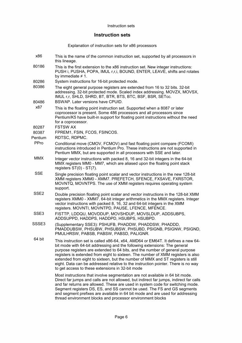
Instruction sets
Explanation of instruction sets for x86 processors
x86
80186
80286 System instructions for 16-bit protected mode.80386
80486 BSWAP. Later versions have CPUID.x87
80287 FSTSW AX80387 FPREM1, FSIN, FCOS, FSINCOS.
Pentium RDTSC, RDPMC.PPro
MMX
SSE
SSE2
SSE3
SSSE3
64 bit
This is the name of the common instruction set, supported by all processors in this lineage.
This is the first extension to the x86 instruction set. New integer instructions: PUSH i, PUSHA, POPA, IMUL r,r,i, BOUND, ENTER, LEAVE, shifts and rotates by immediate ≠ 1.
The eight general purpose registers are extended from 16 to 32 bits. 32-bit addressing. 32-bit protected mode. Scaled index addressing. MOVZX, MOVSX, IMUL r,r, SHLD, SHRD, BT, BTR, BTS, BTC, BSF, BSR, SETcc.
This is the floating point instruction set. Supported when a 8087 or later coprocessor is present. Some 486 processors and all processors since Pentium/K5 have built-in support for floating point instructions without the need for a coprocessor.
Conditional move (CMOV, FCMOV) and fast floating point compare (FCOMI) instructions introduced in Pentium Pro. These instructions are not supported in Pentium MMX, but are supported in all processors with SSE and later.
Integer vector instructions with packed 8, 16 and 32-bit integers in the 64-bit MMX registers MM0 - MM7, which are aliased upon the floating point stack registers ST(0) - ST(7).
Single precision floating point scalar and vector instructions in the new 128-bit XMM registers XMM0 - XMM7. PREFETCH, SFENCE, FXSAVE, FXRSTOR, MOVNTQ, MOVNTPS. The use of XMM registers requires operating system support.
Double precision floating point scalar and vector instructions in the 128-bit XMM registers XMM0 - XMM7. 64-bit integer arithmetics in the MMX registers. Integer vector instructions with packed 8, 16, 32 and 64-bit integers in the XMM registers. MOVNTI, MOVNTPD, PAUSE, LFENCE, MFENCE.
FISTTP, LDDQU, MOVDDUP, MOVSHDUP, MOVSLDUP, ADDSUBPS, ADDSUPPD, HADDPS, HADDPD, HSUBPS, HSUBPD.
(Supplementary SSE3): PSHUFB, PHADDW, PHADDSW, PHADDD, PMADDUBSW, PHSUBW, PHSUBSW, PHSUBD, PSIGNB, PSIGNW, PSIGND, PMULHRSW, PABSB, PABSW, PABSD, PALIGNR.
This instruction set is called x86-64, x64, AMD64 or EM64T. It defines a new 64-bit mode with 64-bit addressing and the following extensions: The general purpose registers are extended to 64 bits, and the number of general purpose registers is extended from eight to sixteen. The number of XMM registers is also extended from eight to sixteen, but the number of MMX and ST registers is still eight. Data can be addressed relative to the instruction pointer. There is no way to get access to these extensions in 32-bit mode
Most instructions that involve segmentation are not available in 64 bit mode. Direct far jumps and calls are not allowed, but indirect far jumps, indirect far calls and far returns are allowed. These are used in system code for switching mode. Segment registers DS, ES, and SS cannot be used. The FS and GS segments and segment prefixes are available in 64 bit mode and are used for addressing thread environment blocks and processor environment blocks

Instruction sets
Page 7
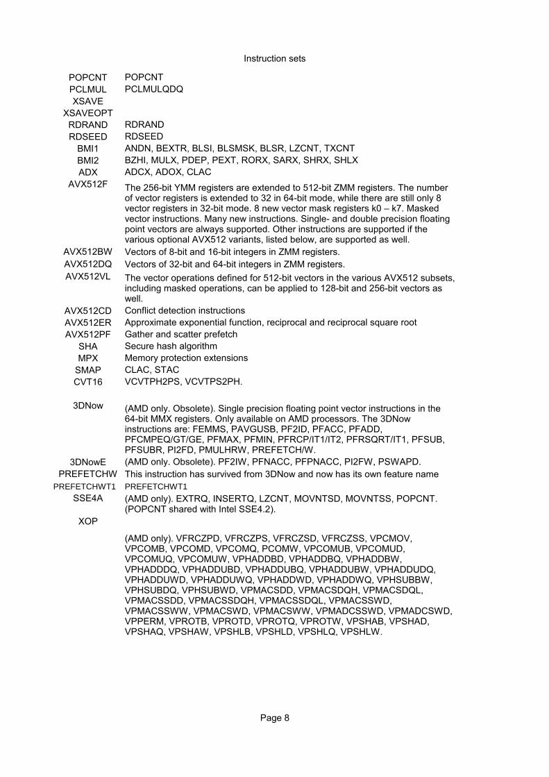
Monitor
SSE4.1
SSE4.2
AES
CLMUL PCLMULQDQ.AVX
AVX2
FMA3
FMA4
MOVBE MOVBE
Instructions not available in 64
bit mode
The following instructions are not available in 64-bit mode: PUSHA, POPA, BOUND, INTO, BCD instructions: AAA, AAS, DAA, DAS, AAD, AAM, undocumented instructions (SALC, ICEBP, 82H alias for 80H opcode), SYSENTER, SYSEXIT, ARPL. On some early Intel processors, LAHF and SAHF are not available in 64 bit mode. Increment and decrement register instructions cannot be coded in the short one-byte opcode form because these codes have been reassigned as REX prefixes.Most instructions that involve segmentation are not available in 64 bit mode. Direct far jumps and calls are not allowed, but indirect far jumps, indirect far calls and far returns are allowed. These are used in system code for switching mode. PUSH CS, PUSH DS, PUSH ES, PUSH SS, POP DS, POP ES, POP SS, LDS and LES instructions are not allowed. CS, DS, ES and SS prefixes are allowed but ignored. The FS and GS segments and segment prefixes are available in 64 bit mode and are used for addressing thread environment blocks and processor environment blocks.The instructions MONITOR and MWAIT are available in some Intel and AMD multiprocessor CPUs with SSE3
MPSADBW, PHMINPOSUW, PMULDQ, PMULLD, DPPS, DPPD, BLEND.., PMIN.., PMAX.., ROUND.., INSERT.., EXTRACT.., PMOVSX.., PMOVZX.., PTEST, PCMPEQQ, PACKUSDW, MOVNTDQA
CRC32, PCMPESTRI, PCMPESTRM, PCMPISTRI, PCMPISTRM, PCMPGTQ, POPCNT.
AESDEC, AESDECLAST, AESENC, AESENCLAST, AESIMC, AESKEYGENASSIST.
The 128-bit XMM registers are extended to 256-bit YMM registers with room for further extension in the future. The use of YMM registers requires operating system support. Floating point vector instructions are available in 256-bit versions. Almost all previous XMM instructions now have two versions: with and without zero-extension into the full YMM register. The zero-extension versions have three operands in most cases. Furthermore, the following instructions are added in AVX: VBROADCASTSS, VBROADCASTSD, VEXTRACTF128, VINSERTF128, VLDMXCSR, VMASKMOVPS, VMASKMOVPD, VPERMILPD, VPERMIL2PD, VPERMILPS, VPERMIL2PS, VPERM2F128, VSTMXCSR, VZEROALL, VZEROUPPER.
Integer vector instructions are available in 256-bit versions. Furthermore, the following instructions are added in AVX2: ANDN, BEXTR, BLSI, BLSMSK, BLSR, BZHI, INVPCID, LZCNT, MULX, PEXT, PDEP, RORX, SARX, SHLX, SHRX, TZCNT, VBROADCASTI128, VBROADCASTSS, VBROADCASTSD, VEXTRACTI128, VGATHERDPD, VGATHERQPD, VGATHERDPS, VGATHERQPS, VPGATHERDD, VPGATHERQD, VPGATHERDQ, VPGATHERQQ, VINSERTI128, VPERM2I128, VPERMD, VPERMPD, VPERMPS, VPERMQ, VPMASKMOVD, VPMASKMOVQ, VPSLLVD, VPSLLVQ, VPSRAVD, VPSRLVD, VPSRLVQ.
(FMA): Fused multiply and add instructions: VFMADDxxxPD, VFMADDxxxPS, VFMADDxxxSD, VFMADDxxxSS, VFMADDSUBxxxPD, VFMADDSUBxxxPS, VFMSUBADDxxxPD, VFMSUBADDxxxPS, VFMSUBxxxPD, VFMSUBxxxPS, VFMSUBxxxSD, VFMSUBxxxSS, VFNMADDxxxPD, VFNMADDxxPS, VFNMADDxxxSD, VFNMADDxxxSS, VFNMSUBxxxPD, VFNMSUBxxxPS, VFNMSUBxxxSD, VFNMSUBxxxSS.
Same as Intel FMA, but with 4 different operands according to a preliminary Intel specification which is now supported only by AMD. Intel's FMA specification has later been changed to FMA3, which is now also supported by AMD.
Instruction sets
Page 8
POPCNT POPCNTPCLMUL PCLMULQDQXSAVE
XSAVEOPTRDRAND RDRANDRDSEED RDSEED
BMI1 ANDN, BEXTR, BLSI, BLSMSK, BLSR, LZCNT, TXCNTBMI2 BZHI, MULX, PDEP, PEXT, RORX, SARX, SHRX, SHLXADX ADCX, ADOX, CLAC
AVX512F
AVX512BW Vectors of 8-bit and 16-bit integers in ZMM registers.AVX512DQ Vectors of 32-bit and 64-bit integers in ZMM registers.AVX512VL
AVX512CD Conflict detection instructionsAVX512ER Approximate exponential function, reciprocal and reciprocal square rootAVX512PF Gather and scatter prefetch
SHA Secure hash algorithmMPX Memory protection extensions
SMAP CLAC, STACCVT16 VCVTPH2PS, VCVTPS2PH.
3DNow
3DNowE (AMD only. Obsolete). PF2IW, PFNACC, PFPNACC, PI2FW, PSWAPD.PREFETCHW This instruction has survived from 3DNow and now has its own feature namePREFETCHWT1 PREFETCHWT1
SSE4A
XOP
The 256-bit YMM registers are extended to 512-bit ZMM registers. The number of vector registers is extended to 32 in 64-bit mode, while there are still only 8 vector registers in 32-bit mode. 8 new vector mask registers k0 – k7. Masked vector instructions. Many new instructions. Single- and double precision floating point vectors are always supported. Other instructions are supported if the various optional AVX512 variants, listed below, are supported as well.
The vector operations defined for 512-bit vectors in the various AVX512 subsets, including masked operations, can be applied to 128-bit and 256-bit vectors as well.
(AMD only. Obsolete). Single precision floating point vector instructions in the 64-bit MMX registers. Only available on AMD processors. The 3DNow instructions are: FEMMS, PAVGUSB, PF2ID, PFACC, PFADD, PFCMPEQ/GT/GE, PFMAX, PFMIN, PFRCP/IT1/IT2, PFRSQRT/IT1, PFSUB, PFSUBR, PI2FD, PMULHRW, PREFETCH/W.
(AMD only). EXTRQ, INSERTQ, LZCNT, MOVNTSD, MOVNTSS, POPCNT. (POPCNT shared with Intel SSE4.2).
(AMD only). VFRCZPD, VFRCZPS, VFRCZSD, VFRCZSS, VPCMOV, VPCOMB, VPCOMD, VPCOMQ, PCOMW, VPCOMUB, VPCOMUD, VPCOMUQ, VPCOMUW, VPHADDBD, VPHADDBQ, VPHADDBW, VPHADDDQ, VPHADDUBD, VPHADDUBQ, VPHADDUBW, VPHADDUDQ, VPHADDUWD, VPHADDUWQ, VPHADDWD, VPHADDWQ, VPHSUBBW, VPHSUBDQ, VPHSUBWD, VPMACSDD, VPMACSDQH, VPMACSDQL, VPMACSSDD, VPMACSSDQH, VPMACSSDQL, VPMACSSWD, VPMACSSWW, VPMACSWD, VPMACSWW, VPMADCSSWD, VPMADCSWD, VPPERM, VPROTB, VPROTD, VPROTQ, VPROTW, VPSHAB, VPSHAD, VPSHAQ, VPSHAW, VPSHLB, VPSHLD, VPSHLQ, VPSHLW.

Microprocessors tested
Page 9
Microprocessor versions tested
The tables in this manual are based on testing of the following microprocessors
Processor name CommentAMD K7 Athlon 6 6 Step. 2, rev. A5AMD K8 Opteron F 5 Stepping AAMD K10 Opteron 10 2 2350, step. 1AMD Bulldozer Bulldozer, Zambezi 15 1 FX-6100, step 2AMD Piledriver Piledriver 15 2 FX-8350, step 0. And othersAMD Steamroller Steamroller, Kaveri 15 30 A10-7850K, step 1AMD Ryzen Zen 17 1 Ryzen 7 1800X, step 1AMD Bobcat Bobcat 14 1 E350, step. 0AMD Kabini Jaguar 16 0 A4-5000, step 1Intel Pentium P5 5 2Intel Pentium MMX P5 5 4 Stepping 4Intel Pentium II P6 6 6Intel Pentium III P6 6 7Intel Pentium 4 Netburst F 2 Stepping 4, rev. B0Intel Pentium 4 EM64T Netburst, Prescott F 4 Xeon. Stepping 1Intel Pentium M Dothan 6 D Stepping 6, rev. B1Intel Core Duo Yonah 6 E Not fully testedIntel Core 2 (65 nm) Merom 6 F T5500, Step. 6, rev. B2Intel Core 2 (45 nm) Wolfdale 6 17 E8400, Step. 6Intel Core i7 Nehalem 6 1A i7-920, Step. 5, rev. D0Intel 2nd gen. Core Sandy Bridge 6 2A i5-2500, Step 7Intel 3rd gen. Core Ivy Bridge 6 3A i7-3770K, Step 9Intel 4th gen. Core Haswell 6 3C i7-4770K, step. 3Intel 5th gen. Core Broadwell 6 56 D1540, step 2Intel 6th gen. Core Skylake 6 5E Step. 3Intel Atom 330 Diamondville 6 1C Step. 2Intel Bay Trail Silvermont 6 37 Step. 3Intel Xeon Phi Knights Landing 6 57 Step. 1VIA Nano L2200 6 F Step. 2VIA Nano L3050 Isaiah 6 F Step. 8 (prerelease sample)
MicroarchitectureCode name
Family number (hex)
Model number (hex)

AMD K7
Page 10
AMD K7List of instruction timings and macro-operation breakdown
Explanation of column headings:Instruction:
Operands:
Ops:
Latency:
Reciprocal throughput:
Execution unit:
Integer instructionsInstruction Operands Ops Latency Notes
Move instructionsMOV r,r 1 1 1/3 ALUMOV r,i 1 1 1/3 ALU
MOV r8,m8 1 4 1/2 ALU, AGUMOV r16,m16 1 4 1/2 ALU, AGU do.MOV r32,m32 1 3 1/2 AGU do.MOV m8,r8H 1 8 1/2 AGU AH, BH, CH, DH
MOV m8,r8L 1 2 1/2 AGU
MOV m16/32,r 1 2 1/2 AGUMOV m,i 1 2 1/2 AGUMOV r,sr 1 2 1
Instruction name. cc means any condition code. For example, Jcc can be JB, JNE, etc.
i = immediate constant, r = any register, r32 = 32-bit register, etc., mm = 64 bit mmx register, xmm = 128 bit xmm register, sr = segment register, m = any memory operand including indirect operands, m64 means 64-bit memory oper-and, etc.
Number of macro-operations issued from instruction decoder to schedulers. In-structions with more than 2 macro-operations use microcode.
This is the delay that the instruction generates in a dependency chain. The numbers are minimum values. Cache misses, misalignment, and exceptions may increase the clock counts considerably. Floating point operands are pre-sumed to be normal numbers. Denormal numbers, NAN's, infinity and excep-tions increase the delays. The latency listed does not include the memory oper-and where the operand is listed as register or memory (r/m).
This is also called issue latency. This value indicates the average number of clock cycles from the execution of an instruction begins to a subsequent inde-pendent instruction of the same kind can begin to execute. A value of 1/3 indi-cates that the execution units can handle 3 instructions per clock cycle in one thread. However, the throughput may be limited by other bottlenecks in the pipeline.
Indicates which execution unit is used for the macro-operations. ALU means any of the three integer ALU's. ALU0_1 means that ALU0 and ALU1 are both used. AGU means any of the three integer address generation units. FADD means floating point adder unit. FMUL means floating point multiplier unit. FMISC means floating point store and miscellaneous unit. FA/M means FADD or FMUL is used. FANY means any of the three floating point units can be used. Two macro-operations can execute simultaneously if they go to different execution units.
Reciprocal throughput
Execution unit
Any addr. mode. Add 1 clk if code segment base ≠ 0
Any other 8-bit register
Any addressing mode

AMD K7
Page 11
MOV sr,r/m 6 9-13 8MOVZX, MOVSX r,r 1 1 1/3 ALUMOVZX, MOVSX r,m 1 4 1/2 ALU, AGUCMOVcc r,r 1 1 1/3 ALUCMOVcc r,m 1 1/2 ALU, AGUXCHG r,r 3 2 1 ALU
XCHG r,m 3 16 16 ALU, AGUXLAT 2 5 ALU, AGUPUSH r 1 1 ALU, AGUPUSH i 1 1 ALU, AGUPUSH m 2 1 ALU, AGUPUSH sr 2 1 ALU, AGUPUSHF(D) 1 1 ALU, AGUPUSHA(D) 9 4 ALU, AGUPOP r 2 1 ALU, AGUPOP m 3 1 ALU, AGUPOP DS/ES/FS/GS 6 10 ALU, AGUPOP SS 9 18 ALU, AGUPOPF(D) 2 1 ALU, AGUPOPA(D) 9 4 ALU, AGULEA r16,[m] 2 3 1 AGU Any addr. sizeLEA r32,[m] 1 2 1/3 AGU Any addr. sizeLAHF 4 3 2 ALUSAHF 2 2 2 ALUSALC 1 1 1 ALULDS, LES, ... r,m 10 9BSWAP r 1 1 1/3 ALU
Arithmetic instructionsADD, SUB r,r/i 1 1 1/3 ALUADD, SUB r,m 1 1 1/2 ALU, AGUADD, SUB m,r 1 7 2,5 ALU, AGUADC, SBB r,r/i 1 1 1/3 ALUADC, SBB r,m 1 1 1/2 ALU, AGUADC, SBB m,r/i 1 7 2,5 ALU, AGUCMP r,r/i 1 1 1/3 ALUCMP r,m 1 1/2 ALU, AGUINC, DEC, NEG r 1 1 1/3 ALUINC, DEC, NEG m 1 7 3 ALU, AGUAAA, AAS 9 5 5 ALUDAA 12 6 6 ALUDAS 16 7 7 ALUAAD 4 5 ALU0AAM 31 13 ALUMUL, IMUL r8/m8 3 3 2 ALU0
MUL, IMUL r16/m16 3 3 2 ALU0_1MUL, IMUL r32/m32 3 4 3 ALU0_1IMUL r16,r16/m16 2 3 2 ALU0
Timing depends on hw
latency ax=3, dx=4

AMD K7
Page 12
IMUL r32,r32/m32 2 4 2,5 ALU0IMUL r16,(r16),i 2 4 1 ALU0IMUL r32,(r32),i 2 5 2 ALU0IMUL r16,m16,i 3 2 ALU0IMUL r32,m32,i 3 2 ALU0DIV r8/m8 32 24 23 ALUDIV r16/m16 47 24 23 ALUDIV r32/m32 79 40 40 ALUIDIV r8 41 17 17 ALUIDIV r16 56 25 25 ALUIDIV r32 88 41 41 ALUIDIV m8 42 17 17 ALUIDIV m16 57 25 25 ALUIDIV m32 89 41 41 ALUCBW, CWDE 1 1 1/3 ALUCWD, CDQ 1 1 1/3 ALU
Logic instructionsAND, OR, XOR r,r 1 1 1/3 ALUAND, OR, XOR r,m 1 1 1/2 ALU, AGUAND, OR, XOR m,r 1 7 2,5 ALU, AGUTEST r,r 1 1 1/3 ALUTEST r,m 1 1 1/2 ALU, AGUNOT r 1 1 1/3 ALUNOT m 1 7 2,5 ALU, AGUSHL, SHR, SAR r,i/CL 1 1 1/3 ALUROL, ROR r,i/CL 1 1 1/3 ALURCL, RCR r,1 1 1 1/3 ALURCL r,i 9 4 4 ALURCR r,i 7 3 3 ALURCL r,CL 9 3 3 ALURCR r,CL 7 3 3 ALUSHL,SHR,SAR,ROL,ROR m,i /CL 1 7 3 ALU, AGURCL, RCR m,1 1 7 4 ALU, AGURCL m,i 10 5 4 ALU, AGURCR m,i 9 8 4 ALU, AGURCL m,CL 9 6 4 ALU, AGURCR m,CL 8 7 3 ALU, AGUSHLD, SHRD r,r,i 6 4 2 ALUSHLD, SHRD r,r,cl 7 4 3 ALUSHLD, SHRD m,r,i/CL 8 7 3 ALU, AGUBT r,r/i 1 1 1/3 ALUBT m,i 1 1/2 ALU, AGUBT m,r 5 2 ALU, AGUBTC, BTR, BTS r,r/i 2 2 1 ALUBTC m,i 5 7 2 ALU, AGUBTR, BTS m,i 4 7 2 ALU, AGUBTC, BTR, BTS m,r 8 6 3 ALU, AGUBSF r,r 19 7 7 ALUBSR r,r 23 9 9 ALU

AMD K7
Page 13
BSF r,m 20 8 8 ALU, AGUBSR r,m 23 10 10 ALU, AGUSETcc r 1 1 1/3 ALUSETcc m 1 1/2 ALU, AGUCLC, STC 1 1/3 ALUCMC 1 1 1/3 ALUCLD 2 1 ALUSTD 3 2 ALU
Control transfer instructionsJMP short/near 1 2 ALU
JMP far 16-20 23-32JMP r 1 2 ALUJMP m(near) 1 2 ALU, AGU
JMP m(far) 17-21 25-33Jcc short/near 1 1/3 - 2 ALU rcp. t.= 2 if jumpJ(E)CXZ short 2 1/3 - 2 ALU rcp. t.= 2 if jumpLOOP short 7 3-4 3-4 ALUCALL near 3 2 2 ALU
CALL far 16-22 23-32CALL r 4 3 3 ALUCALL m(near) 5 3 3 ALU, AGU
CALL m(far) 16-22 24-33RETN 2 3 3 ALURETN i 2 3 3 ALU
RETF 15-23 24-35
RETF i 15-24 24-35IRET 32 81 real modeINT i 33 42 real mode
BOUND m 6 2
INTO 2 2
String instructionsLODS 4 2 2REP LODS 5 2 2 values per countSTOS 4 2 2REP STOS 3 1 1 values per countMOVS 7 3 3REP MOVS 4 1-4 1-4 values per countSCAS 5 2 2REP SCAS 5 2 2 values per countCMPS 7 6 6REP CMPS 6 3-4 3-4 values per count
low values = real mode
low values = real mode
low values = real mode
low values = real mode
low values = real mode
low values = real mode
values are for no jump
values are for no jump

AMD K7
Page 14
OtherNOP (90) 1 0 1/3 ALULong NOP (0F 1F) 1 0 1/3 ALUENTER i,0 12 12 12
LEAVE 3 3CLI 8-9 5STI 16-17 27CPUID 19-28 44-74RDTSC 5 11RDPMC 9 11
Floating point x87 instructionsInstruction Operands Ops Latency Notes
Move instructionsFLD r 1 2 1/2 FA/MFLD m32/64 1 4 1/2 FANYFLD m80 7 16 4FBLD m80 30 41 39FST(P) r 1 2 1/2 FA/MFST(P) m32/64 1 3 1 FMISCFSTP m80 10 7 5FBSTP m80 260 188FXCH r 1 0 0,4FILD m 1 9 1 FMISCFIST(P) m 1 7 1 FMISC, FA/M
FLDZ, FLD1 1 1 FMISC
FCMOVcc st0,r 9 6 5 FMISC, FA/M
FFREE r 1 1/3 FANYFINCSTP, FDECSTP 1 0 1/3 FANY
FNSTSW AX 2 6-12 12 FMISC, ALUFSTSW AX 3 6-12 12 FMISC, ALU do.FNSTSW m16 2 8 FMISC, ALU do.FNSTCW m16 3 1 FMISC, ALU
FLDCW m16 14 42 FMISC, ALU
Arithmetic instructionsFADD(P),FSUB(R)(P) r/m 1 4 1 FADDFIADD,FISUB(R) m 2 4 1-2 FADD,FMISCFMUL(P) r/m 1 4 1 FMULFIMUL m 2 4 2 FMUL,FMISC
FDIV(R)(P) r/m 1 11-25 8-22 FMUL
3 ops, 5 clk if 16 bit
Reciprocal throughput
Execution unit
Low latency im-mediately after FCOMI
Low latency im-mediately after FCOM FTST
faster if unchanged
Low values are for round divisors
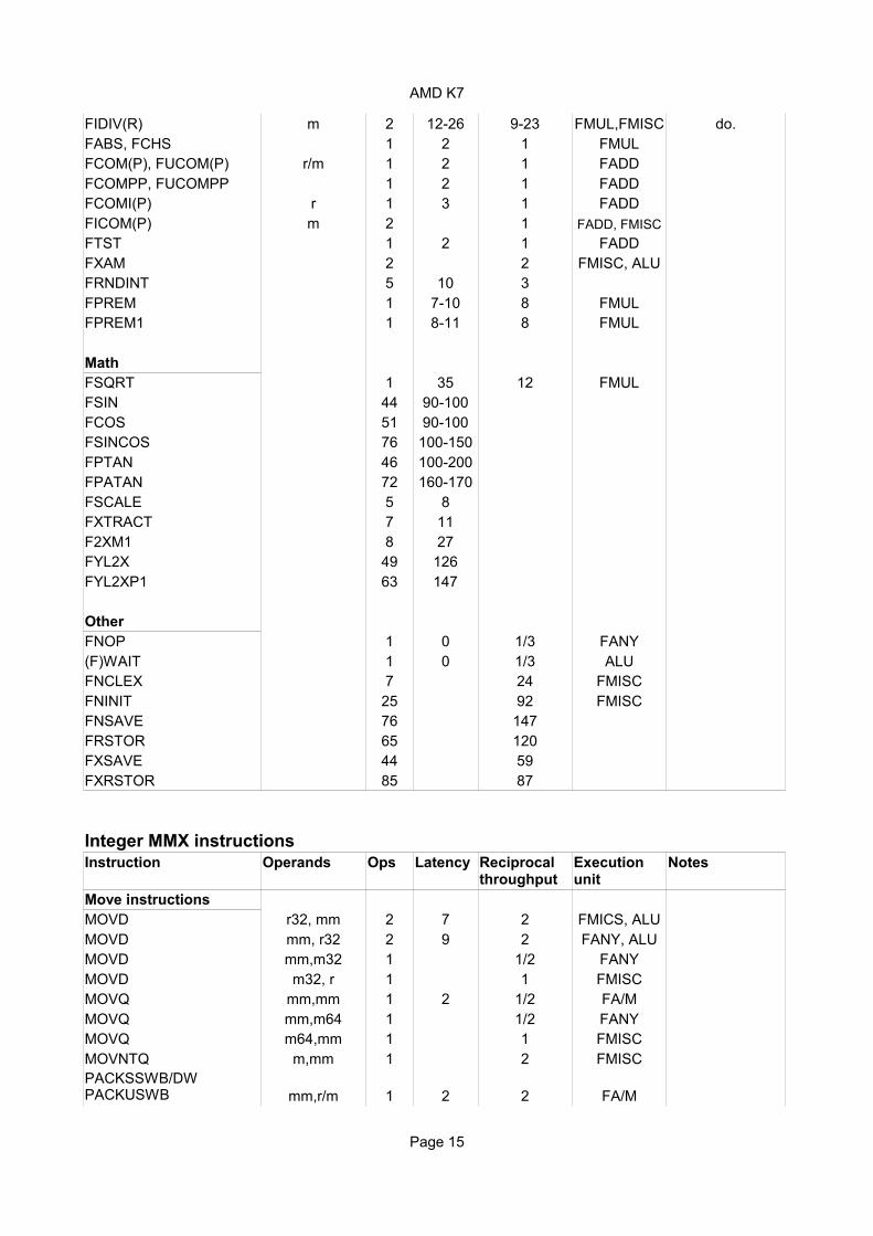
AMD K7
Page 15
FIDIV(R) m 2 12-26 9-23 FMUL,FMISC do.FABS, FCHS 1 2 1 FMULFCOM(P), FUCOM(P) r/m 1 2 1 FADDFCOMPP, FUCOMPP 1 2 1 FADDFCOMI(P) r 1 3 1 FADDFICOM(P) m 2 1 FADD, FMISC
FTST 1 2 1 FADDFXAM 2 2 FMISC, ALUFRNDINT 5 10 3FPREM 1 7-10 8 FMULFPREM1 1 8-11 8 FMUL
MathFSQRT 1 35 12 FMULFSIN 44 90-100FCOS 51 90-100FSINCOS 76 100-150FPTAN 46 100-200FPATAN 72 160-170FSCALE 5 8FXTRACT 7 11F2XM1 8 27FYL2X 49 126FYL2XP1 63 147
OtherFNOP 1 0 1/3 FANY(F)WAIT 1 0 1/3 ALUFNCLEX 7 24 FMISCFNINIT 25 92 FMISCFNSAVE 76 147FRSTOR 65 120FXSAVE 44 59FXRSTOR 85 87
Integer MMX instructionsInstruction Operands Ops Latency Notes
Move instructionsMOVD r32, mm 2 7 2 FMICS, ALUMOVD mm, r32 2 9 2 FANY, ALUMOVD mm,m32 1 1/2 FANYMOVD m32, r 1 1 FMISCMOVQ mm,mm 1 2 1/2 FA/MMOVQ mm,m64 1 1/2 FANYMOVQ m64,mm 1 1 FMISCMOVNTQ m,mm 1 2 FMISC
mm,r/m 1 2 2 FA/M
Reciprocal throughput
Execution unit
PACKSSWB/DW PACKUSWB

AMD K7
Page 16
PUNPCKH/LBW/WD mm,r/m 1 2 2 FA/MPSHUFW mm,mm,i 1 2 1/2 FA/MMASKMOVQ mm,mm 32 24PMOVMSKB r32,mm 3 3 FADDPEXTRW r32,mm,i 2 5 2 FMISC, ALUPINSRW mm,r32,i 2 12 2 FA/M
Arithmetic instructions
mm,r/m 1 2 1/2 FA/MPCMPEQ/GT B/W/D mm,r/m 1 2 1/2 FA/M
mm,r/m 1 3 1 FMULPMADDWD mm,r/m 1 3 1 FMULPAVGB/W mm,r/m 1 2 1/2 FA/MPMIN/MAX SW/UB mm,r/m 1 2 1/2 FA/MPSADBW mm,r/m 1 3 1 FADD
Logic
mm,r/m 1 2 1/2 FA/M
mm,i/mm/m 1 2 1/2 FA/M
OtherEMMS 1 1/3 FANY
Floating point XMM instructionsInstruction Operands Ops Latency Notes
Move instructionsMOVAPS r,r 2 2 1 FA/MMOVAPS r,m 2 2 FMISCMOVAPS m,r 2 2 FMISCMOVUPS r,r 2 2 1 FA/MMOVUPS r,m 5 2MOVUPS m,r 5 2MOVSS r,r 1 2 1 FA/MMOVSS r,m 2 4 1 FANY FMISCMOVSS m,r 1 3 1 FMISCMOVHLPS, MOVLHPS r,r 1 2 1/2 FA/MMOVHPS, MOVLPS r,m 1 1/2 FMISCMOVHPS, MOVLPS m,r 1 1 FMISCMOVNTPS m,r 2 4 FMISCMOVMSKPS r32,r 3 2 FADDSHUFPS r,r/m,i 3 3 3 FMUL
PADDB/W/D PADDSB/W PADDUSB/W PSUBB/W/D PSUBSB/W PSUBUSB/W
PMULLW PMULHW PMULHUW
PAND PANDN POR PXOR
PSLL/RLW/D/Q PSRAW/D
Reciprocal throughput
Execution unit
AMD K7
Page 17
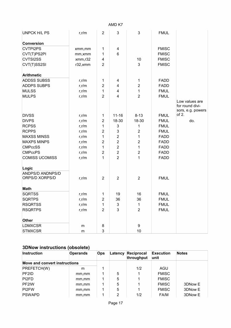
UNPCK H/L PS r,r/m 2 3 3 FMUL
ConversionCVTPI2PS xmm,mm 1 4 FMISCCVT(T)PS2PI mm,xmm 1 6 FMISCCVTSI2SS xmm,r32 4 10 FMISCCVT(T)SS2SI r32,xmm 2 3 FMISC
ArithmeticADDSS SUBSS r,r/m 1 4 1 FADDADDPS SUBPS r,r/m 2 4 2 FADDMULSS r,r/m 1 4 1 FMULMULPS r,r/m 2 4 2 FMUL
DIVSS r,r/m 1 11-16 8-13 FMULDIVPS r,r/m 2 18-30 18-30 FMUL do.RCPSS r,r/m 1 3 1 FMULRCPPS r,r/m 2 3 2 FMULMAXSS MINSS r,r/m 1 2 1 FADDMAXPS MINPS r,r/m 2 2 2 FADDCMPccSS r,r/m 1 2 1 FADDCMPccPS r,r/m 2 2 2 FADDCOMISS UCOMISS r,r/m 1 2 1 FADD
Logic
r,r/m 2 2 2 FMUL
MathSQRTSS r,r/m 1 19 16 FMULSQRTPS r,r/m 2 36 36 FMULRSQRTSS r,r/m 1 3 1 FMULRSQRTPS r,r/m 2 3 2 FMUL
OtherLDMXCSR m 8 9STMXCSR m 3 10
3DNow instructions (obsolete)Instruction Operands Ops Latency Notes
Move and convert instructionsPREFETCH(W) m 1 1/2 AGUPF2ID mm,mm 1 5 1 FMISCPI2FD mm,mm 1 5 1 FMISCPF2IW mm,mm 1 5 1 FMISC 3DNow EPI2FW mm,mm 1 5 1 FMISC 3DNow EPSWAPD mm,mm 1 2 1/2 FA/M 3DNow E
Low values are for round divi-sors, e.g. powers of 2.
ANDPS/D ANDNPS/D ORPS/D XORPS/D
Reciprocal throughput
Execution unit

AMD K7
Page 18
Integer instructionsPAVGUSB mm,mm 1 2 1/2 FA/MPMULHRW mm,mm 1 3 1 FMUL
Floating point instructionsPFADD/SUB/SUBR mm,mm 1 4 1 FADDPFCMPEQ/GE/GT mm,mm 1 2 1 FADDPFMAX/MIN mm,mm 1 2 1 FADDPFMUL mm,mm 1 4 1 FMULPFACC mm,mm 1 4 1 FADDPFNACC, PFPNACC mm,mm 1 4 1 FADD 3DNow EPFRCP mm,mm 1 3 1 FMULPFRCPIT1/2 mm,mm 1 4 1 FMULPFRSQRT mm,mm 1 3 1 FMULPFRSQIT1 mm,mm 1 4 1 FMUL
OtherFEMMS mm,mm 1 1/3 FANY

K8
Page 19
AMD K8List of instruction timings and macro-operation breakdown
Explanation of column headings:Instruction:
Operands:
Ops:
Latency:
Execution unit:
Integer instructionsInstruction Operands Ops Latency Notes
Move instructionsMOV r,r 1 1 1/3 ALUMOV r,i 1 1 1/3 ALUMOV r8,m8 1 4 1/2 ALU, AGUMOV r16,m16 1 4 1/2 ALU, AGUMOV r32,m32 1 3 1/2 AGUMOV r64,m64 1 3 1/2 AGUMOV m8,r8H 1 8 1/2 AGU AH, BH, CH, DH
MOV m8,r8L 1 3 1/2 AGUMOV m16/32/64,r 1 3 1/2 AGU Any addressing modeMOV m,i 1 3 1/2 AGUMOV m64,i32 1 3 1/2 AGUMOV r,sr 1 2 1/2-1MOV sr,r/m 6 9-13 8MOVNTI m,r 1 2-3 AGU
Instruction name. cc means any condition code. For example, Jcc can be JB, JNE, etc.
i = immediate constant, r = any register, r32 = 32-bit register, etc., mm = 64 bit mmx register, xmm = 128 bit xmm register, sr = segment register, m = any mem-ory operand including indirect operands, m64 means 64-bit memory operand, etc.
Number of macro-operations issued from instruction decoder to schedulers. In-structions with more than 2 macro-operations use microcode.
This is the delay that the instruction generates in a dependency chain. The num-bers are minimum values. Cache misses, misalignment, and exceptions may in-crease the clock counts considerably. Floating point operands are presumed to be normal numbers. Denormal numbers, NAN's, infinity and exceptions increase the delays. The latency listed does not include the memory operand where the oper-and is listed as register or memory (r/m).
Reciprocal through-put:
This is also called issue latency. This value indicates the average number of clock cycles from the execution of an instruction begins to a subsequent independent instruction of the same kind can begin to execute. A value of 1/3 indicates that the execution units can handle 3 instructions per clock cycle in one thread. However, the throughput may be limited by other bottlenecks in the pipeline.
Indicates which execution unit is used for the macro-operations. ALU means any of the three integer ALU's. ALU0_1 means that ALU0 and ALU1 are both used. AGU means any of the three integer address generation units. FADD means float-ing point adder unit. FMUL means floating point multiplier unit. FMISC means floating point store and miscellaneous unit. FA/M means FADD or FMUL is used. FANY means any of the three floating point units can be used. Two macro-opera-tions can execute simultaneously if they go to different execution units.
Reciprocal throughput
Execution unit
Any addressing mode. Add 1 clock if code segment base ≠ 0
Any other 8-bit regis-ter

K8
Page 20
MOVZX, MOVSX r,r 1 1 1/3 ALUMOVZX, MOVSX r,m 1 4 1/2 ALU, AGUMOVSXD r64,r32 1 1 1/3 ALUMOVSXD r64,m32 1 1/2 ALU, AGUCMOVcc r,r 1 1 1/3 ALUCMOVcc r,m 1 1/2 ALU, AGUXCHG r,r 3 2 1 ALU
XCHG r,m 3 16 16 ALU, AGUXLAT 2 5 ALU, AGUPUSH r 1 1 1 ALU, AGUPUSH i 1 1 1 ALU, AGUPUSH m 2 1 1 ALU, AGUPUSH sr 2 1 1 ALU, AGUPUSHF(D/Q) 5 2 2 ALU, AGUPUSHA(D) 9 4 4 ALU, AGUPOP r 2 1 1 ALU, AGUPOP m 3 1 1 ALU, AGUPOP DS/ES/FS/GS 4-6 8 8 ALU, AGUPOP SS 7-9 28 28 ALU, AGUPOPF(D/Q) 25 10 10 ALU, AGUPOPA(D) 9 4 4 ALU, AGULEA r16,[m] 2 3 1 AGU Any address sizeLEA r32,[m] 1 2 1/3 AGU Any address sizeLEA r64,[m] 1 2 1/3 AGU Any address sizeLAHF 4 3 2 ALUSAHF 1 1 1/3 ALUSALC 1 1 1/3 ALULDS, LES, ... r,m 10 9BSWAP r 1 1 1/3 ALUPREFETCHNTA m 1 1/2 AGUPREFETCHT0/1/2 m 1 1/2 AGUSFENCE 6 8LFENCE 1 5MFENCE 7 16IN r,i/DX 270OUT i/DX,r 300
Arithmetic instructionsADD, SUB r,r/i 1 1 1/3 ALUADD, SUB r,m 1 1 1/2 ALU, AGUADD, SUB m,r 1 7 2,5 ALU, AGUADC, SBB r,r/i 1 1 1/3 ALUADC, SBB r,m 1 1 1/2 ALU, AGUADC, SBB m,r/i 1 7 2,5 ALU, AGUCMP r,r/i 1 1 1/3 ALUCMP r,m 1 1/2 ALU, AGUINC, DEC, NEG r 1 1 1/3 ALUINC, DEC, NEG m 1 7 3 ALU, AGUAAA, AAS 9 5 5 ALUDAA 12 6 6 ALUDAS 16 7 7 ALUAAD 4 5 ALU0
Timing depends on hw

K8
Page 21
AAM 31 13 ALUMUL, IMUL r8/m8 1 3 1 ALU0MUL, IMUL r16/m16 3 3-4 2 ALU0_1 latency ax=3, dx=4MUL, IMUL r32/m32 2 3 1 ALU0_1MUL, IMUL r64/m64 2 4-5 2 ALU0_1 latency rax=4, rdx=5IMUL r16,r16/m16 1 3 1 ALU0IMUL r32,r32/m32 1 3 1 ALU0IMUL r64,r64/m64 1 4 2 ALU0_1IMUL r16,(r16),i 2 4 1 ALU0IMUL r32,(r32),i 1 3 1 ALU0IMUL r64,(r64),i 1 4 2 ALU0IMUL r16,m16,i 3 2 ALU0IMUL r32,m32,i 3 2 ALU0IMUL r64,m64,i 3 2 ALU0_1DIV r8/m8 31 15 15 ALUDIV r16/m16 46 23 23 ALUDIV r32/m32 78 39 39 ALUDIV r64/m64 143 71 71 ALUIDIV r8 40 17 17 ALUIDIV r16 55 25 25 ALUIDIV r32 87 41 41 ALUIDIV r64 152 73 73 ALUIDIV m8 41 17 17 ALUIDIV m16 56 25 25 ALUIDIV m32 88 41 41 ALUIDIV m64 153 73 73 ALUCBW, CWDE, CDQE 1 1 1/3 ALUCWD, CDQ, CQO 1 1 1/3 ALU
Logic instructionsAND, OR, XOR r,r 1 1 1/3 ALUAND, OR, XOR r,m 1 1 1/2 ALU, AGUAND, OR, XOR m,r 1 7 2,5 ALU, AGUTEST r,r 1 1 1/3 ALUTEST r,m 1 1 1/2 ALU, AGUNOT r 1 1 1/3 ALUNOT m 1 7 2,5 ALU, AGUSHL, SHR, SAR r,i/CL 1 1 1/3 ALUROL, ROR r,i/CL 1 1 1/3 ALURCL, RCR r,1 1 1 1/3 ALURCL r,i 9 3 3 ALURCR r,i 7 3 3 ALURCL r,CL 9 4 4 ALURCR r,CL 7 3 3 ALU
m,i /CL 1 7 3 ALU, AGURCL, RCR m,1 1 7 4 ALU, AGURCL m,i 10 9 4 ALU, AGURCR m,i 9 8 4 ALU, AGURCL m,CL 9 7 4 ALU, AGURCR m,CL 8 8 3 ALU, AGUSHLD, SHRD r,r,i 6 3 3 ALUSHLD, SHRD r,r,cl 7 3 3 ALU
SHL,SHR,SAR,ROL,ROR

K8
Page 22
SHLD, SHRD m,r,i/CL 8 6 3 ALU, AGUBT r,r/i 1 1 1/3 ALUBT m,i 1 1/2 ALU, AGUBT m,r 5 2 ALU, AGUBTC, BTR, BTS r,r/i 2 2 1 ALUBTC m,i 5 7 2 ALU, AGUBTR, BTS m,i 4 7 2 ALU, AGUBTC m,r 8 5 5 ALU, AGUBTR, BTS m,r 8 8 3 ALU, AGUBSF r16/32,r 21 8 8 ALUBSF r64,r 22 9 9 ALUBSR r,r 28 10 10 ALUBSF r16,m 20 8 8 ALU, AGUBSF r32,m 22 9 9 ALU, AGUBSF r64,m 25 10 10 ALU, AGUBSR r,m 28 10 10 ALU, AGUSETcc r 1 1 1/3 ALUSETcc m 1 1/2 ALU, AGUCLC, STC 1 1/3 ALUCMC 1 1 1/3 ALUCLD 1 1/3 ALUSTD 2 1/3 ALU
Control transfer instructionsJMP short/near 1 2 ALU
JMP far 16-20 23-32JMP r 1 2 ALUJMP m(near) 1 2 ALU, AGU
JMP m(far) 17-21 25-33Jcc short/near 1 1/3 - 2 ALU recip. thrp.= 2 if jumpJ(E/R)CXZ short 2 1/3 - 2 ALU recip. thrp.= 2 if jumpLOOP short 7 3-4 3-4 ALUCALL near 3 2 2 ALU
CALL far 16-22 23-32CALL r 4 3 3 ALUCALL m(near) 5 3 3 ALU, AGU
CALL m(far) 16-22 24-33RETN 2 3 3 ALURETN i 2 3 3 ALU
RETF 15-23 24-35
RETF i 15-24 24-35IRET 32 81 real modeINT i 33 42 real modeBOUND m 6 2 values are for no jumpINTO 2 2 values are for no jump
String instructions
low values = real mode
low values = real mode
low values = real mode
low values = real mode
low values = real mode
low values = real mode

K8
Page 23
LODS 4 2 2REP LODS 5 2 2 values are per countSTOS 4 2 2REP STOS 1.5 - 2 0.5 - 1 0.5 - 1 values are per countMOVS 7 3 3REP MOVS 3 1-2 1-2 values are per countSCAS 5 2 2REP SCAS 5 2 2 values are per countCMPS 2 3 3REP CMPS 6 2 2 values are per count
OtherNOP (90) 1 0 1/3 ALULong NOP (0F 1F) 1 0 1/3 ALUENTER i,0 12 12 12LEAVE 2 3 3 ops, 5 clk if 16 bitCLI 8-9 5STI 16-17 27CPUID 22-50 47-164RDTSC 6 10 7RDPMC 9 12 7
Floating point x87 instructionsInstruction Operands Ops Latency Notes
Move instructionsFLD r 1 2 1/2 FA/MFLD m32/64 1 4 1/2 FANYFLD m80 7 16 4FBLD m80 30 41 39FST(P) r 1 2 1/2 FA/MFST(P) m32/64 1 3 1 FMISCFSTP m80 10 7 5FBSTP m80 260 173 160FXCH r 1 0 0,4FILD m 1 9 1 FMISCFIST(P) m 1 7 1 FMISC, FA/MFLDZ, FLD1 1 1 FMISC
FCMOVcc st0,r 9 4-15 4 FMISC, FA/MFFREE r 1 2 FANYFINCSTP, FDECSTP 1 0 1/3 FANY
FNSTSW AX 2 6-12 12 FMISC, ALUFSTSW AX 3 6-12 12 FMISC, ALU do.FNSTSW m16 2 8 FMISC, ALU do.FNSTCW m16 3 1 FMISC, ALUFLDCW m16 18 50 FMISC, ALU faster if unchanged
Arithmetic instructionsFADD(P),FSUB(R)(P) r/m 1 4 1 FADD
Reciprocal throughput
Execution unit
Low latency immedi-ately after FCOMI
Low latency immedi-ately after FCOM FTST

K8
Page 24
FIADD,FISUB(R) m 2 4 1-2 FADD,FMISCFMUL(P) r/m 1 4 1 FMULFIMUL m 2 4 2 FMUL,FMISC
FDIV(R)(P) r/m 1 11-25 8-22 FMULFIDIV(R) m 2 12-26 9-23 FMUL,FMISC do.FABS, FCHS 1 2 1 FMULFCOM(P), FUCOM(P) r/m 1 2 1 FADDFCOMPP, FUCOMPP 1 2 1 FADDFCOMI(P) r 1 3 1 FADDFICOM(P) m 2 1 FADD, FMISCFTST 1 2 1 FADDFXAM 2 1 FMISC, ALUFRNDINT 5 10 3FPREM 1 7-10 8 FMULFPREM1 1 8-11 8 FMUL
MathFSQRT 1 27 12 FMULFLDPI, etc. 1 1 FMISCFSIN 66 140-190FCOS 73 150-190FSINCOS 98 170-200FPTAN 67 150-180FPATAN 97 217FSCALE 5 8FXTRACT 7 12 7F2XM1 53 126FYL2X 72 179FYL2XP1 75 175
OtherFNOP 1 0 1/3 FANY(F)WAIT 1 0 1/3 ALUFNCLEX 8 27 FMISCFNINIT 26 100 FMISCFNSAVE 77 171FRSTOR 70 136FXSAVE 61 56FXRSTOR 101 95
Integer MMX and XMM instructionsInstruction Operands Ops Latency Notes
Move instructionsMOVD r32, mm 2 4 2 FMICS, ALUMOVD mm, r32 2 9 2 FANY, ALUMOVD mm,m32 1 1/2 FANYMOVD r32, xmm 3 2 2 FMISC, ALUMOVD xmm, r32 3 3 2MOVD xmm,m32 2 1 FANYMOVD m32, r 1 1 FMISC
Low values are for round divisors
Reciprocal throughput
Execution unit

K8
Page 25
MOVD (MOVQ) r64,mm/xmm 2 4 2 FMISC, ALUMOVD (MOVQ) mm,r64 2 9 2 FANY, ALU do.MOVD (MOVQ) xmm,r64 3 9 2 FANY, ALU do.MOVQ mm,mm 1 2 1/2 FA/MMOVQ xmm,xmm 2 2 1 FA/M, FMISCMOVQ mm,m64 1 1/2 FANYMOVQ xmm,m64 2 1 FANY, FMISCMOVQ m64,mm/x 1 1 FMISCMOVDQA xmm,xmm 2 2 1 FA/MMOVDQA xmm,m 2 2 FMISCMOVDQA m,xmm 2 2 FMISCMOVDQU xmm,m 4 2MOVDQU m,xmm 5 2MOVDQ2Q mm,xmm 1 2 1/2 FA/MMOVQ2DQ xmm,mm 2 2 1 FA/M, FMISCMOVNTQ m,mm 1 2 FMISCMOVNTDQ m,xmm 2 3 FMISC
mm,r/m 1 2 2 FA/M
xmm,r/m 3 3 2 FA/M
mm,r/m 1 2 2 FA/M
xmm,r/m 2 2 2 FA/MPUNPCKHQDQ xmm,r/m 2 2 1 FA/MPUNPCKLQDQ xmm,r/m 1 2 1/2 FA/MPSHUFD xmm,xmm,i 3 3 1,5 FA/MPSHUFW mm,mm,i 1 2 1/2 FA/MPSHUFL/HW xmm,xmm,i 2 2 1 FA/MMASKMOVQ mm,mm 32 13MASKMOVDQU xmm,xmm 64 26PMOVMSKB r32,mm/xmm 1 2 1 FADDPEXTRW r32,mm/x,i 2 5 2 FMISC, ALUPINSRW mm,r32,i 2 12 2 FA/MPINSRW xmm,r32,i 3 12 3 FA/M
Arithmetic instructions
mm,r/m 1 2 1/2 FA/M
xmm,r/m 2 2 1 FA/MPCMPEQ/GT B/W/D mm,r/m 1 2 1/2 FA/MPCMPEQ/GT B/W/D xmm,r/m 2 2 1 FA/M
Moves 64 bits.Name of instruction differs
PACKSSWB/DW PACKUSWB
PACKSSWB/DW PACKUSWB
PUNPCKH/LBW/WD/DQ
PUNPCKH/LBW/WD/DQ
PADDB/W/D/Q PADDSB/W PADDUSB/W PSUBB/W/D/Q PSUBSB/W PSUBUSB/W
PADDB/W/D/Q PADDSB/W ADDUSB/W PSUBB/W/D/Q PSUBSB/W PSUBUSB/W

K8
Page 26
mm,r/m 1 3 1 FMUL
xmm,r/m 2 3 2 FMULPMADDWD mm,r/m 1 3 1 FMULPMADDWD xmm,r/m 2 3 2 FMULPAVGB/W mm,r/m 1 2 1/2 FA/MPAVGB/W xmm,r/m 2 2 1 FA/MPMIN/MAX SW/UB mm,r/m 1 2 1/2 FA/MPMIN/MAX SW/UB xmm,r/m 2 2 1 FA/MPSADBW mm,r/m 1 3 1 FADDPSADBW xmm,r/m 2 3 2 FADD
Logic
mm,r/m 1 2 1/2 FA/M
xmm,r/m 2 2 1 FA/M
mm,i/mm/m 1 2 1/2 FA/M
x,i/x/m 2 2 1 FA/MPSLLDQ, PSRLDQ xmm,i 2 2 1 FA/M
OtherEMMS 1 1/3 FANY
Floating point XMM instructionsInstruction Operands Ops Latency Notes
Move instructionsMOVAPS/D r,r 2 2 1 FA/MMOVAPS/D r,m 2 2 FMISCMOVAPS/D m,r 2 2 FMISCMOVUPS/D r,r 2 2 1 FA/MMOVUPS/D r,m 4 2MOVUPS/D m,r 5 2MOVSS/D r,r 1 2 1 FA/MMOVSS/D r,m 2 4 1 FANY FMISCMOVSS/D m,r 1 3 1 FMISC
r,r 1 2 1/2 FA/M
r,m 1 1 FMISC
m,r 1 1 FMISCMOVDDUP r,r 2 2 1 SSE3MOVSH/LDUP r,r 2 2 2 SSE3MOVNTPS/D m,r 2 3 FMISCMOVMSKPS/D r32,r 1 8 1 FADD
PMULLW PMULHW PMULHUW PMULUDQ
PMULLW PMULHW PMULHUW PMULUDQ
PAND PANDN POR PXOR
PAND PANDN POR PXOR
PSLL/RL W/D/Q PSRAW/D
PSLL/RL W/D/Q PSRAW/D
Reciprocal throughput
Execution unit
MOVHLPS, MOVLHPS
MOVHPS/D, MOVLPS/D
MOVHPS/D, MOVLPS/D

K8
Page 27
SHUFPS/D r,r/m,i 3 3 2 FMULUNPCK H/L PS/D r,r/m 2 3 3 FMUL
ConversionCVTPS2PD r,r/m 2 4 2 FMISCCVTPD2PS r,r/m 4 8 3 FMISCCVTSD2SS r,r/m 3 8 8 FMISCCVTSS2SD r,r/m 1 2 1 FMISCCVTDQ2PS r,r/m 2 5 2 FMISCCVTDQ2PD r,r/m 2 5 2 FMISCCVT(T)PS2DQ r,r/m 2 5 2 FMISCCVT(T)PD2DQ r,r/m 4 8 3 FMISCCVTPI2PS xmm,mm 1 4 1 FMISCCVTPI2PD xmm,mm 2 5 2 FMISCCVT(T)PS2PI mm,xmm 1 6 1 FMISCCVT(T)PD2PI mm,xmm 3 8 2 FMISCCVTSI2SS xmm,r32 3 14 2 FMISCCVTSI2SD xmm,r32 2 12 2 FMISCCVT(T)SD2SI r32,xmm 2 10 2 FMISCCVT(T)SS2SI r32,xmm 2 9 2 FMISC
ArithmeticADDSS/D SUBSS/D r,r/m 1 4 1 FADDADDPS/D SUBPS/D r,r/m 2 4 2 FADD
r,r/m 2 4 2 FADD SSE3MULSS/D r,r/m 1 4 1 FMULMULPS/D r,r/m 2 4 2 FMUL
DIVSS r,r/m 1 11-16 8-13 FMULDIVPS r,r/m 2 18-30 18-30 FMUL do.DIVSD r,r/m 1 11-20 8-17 FMUL do.DIVPD r,r/m 2 16-34 16-34 FMUL do.RCPSS r,r/m 1 3 1 FMULRCPPS r,r/m 2 3 2 FMULMAXSS/D MINSS/D r,r/m 1 2 1 FADDMAXPS/D MINPS/D r,r/m 2 2 2 FADDCMPccSS/D r,r/m 1 2 1 FADDCMPccPS/D r,r/m 2 2 2 FADD
r,r/m 1 2 1 FADD
Logic
r,r/m 2 2 2 FMUL
MathSQRTSS r,r/m 1 19 16 FMULSQRTPS r,r/m 2 36 36 FMULSQRTSD r,r/m 1 27 24 FMULSQRTPD r,r/m 2 48 48 FMULRSQRTSS r,r/m 1 3 1 FMUL
HADDPS/D HSUBPS/D
Low values are for round divisors, e.g. powers of 2.
COMISS/D UCOMISS/D
ANDPS/D ANDNPS/D ORPS/D XORPS/D

K8
Page 28
RSQRTPS r,r/m 2 3 2 FMUL
OtherLDMXCSR m 8 9STMXCSR m 3 10
K10
Page 29
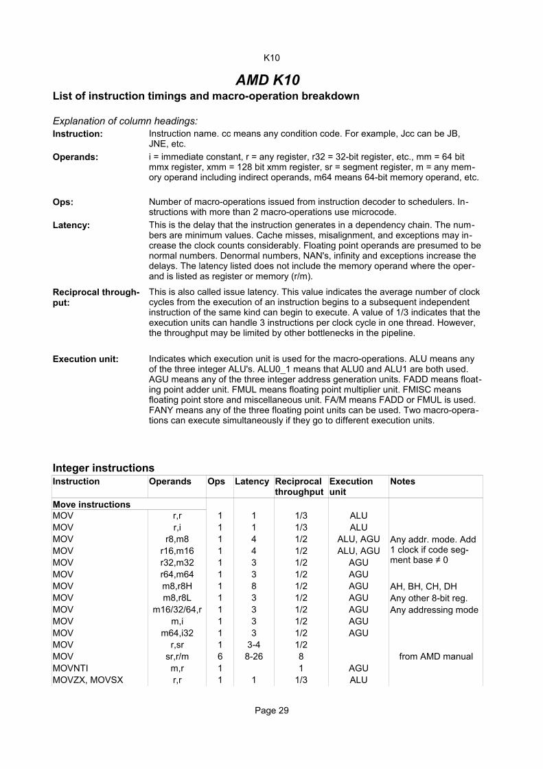
AMD K10List of instruction timings and macro-operation breakdown
Explanation of column headings:Instruction:
Operands:
Ops:
Latency:
Execution unit:
Integer instructionsInstruction Operands Ops Latency Notes
Move instructionsMOV r,r 1 1 1/3 ALUMOV r,i 1 1 1/3 ALUMOV r8,m8 1 4 1/2 ALU, AGUMOV r16,m16 1 4 1/2 ALU, AGUMOV r32,m32 1 3 1/2 AGUMOV r64,m64 1 3 1/2 AGUMOV m8,r8H 1 8 1/2 AGU AH, BH, CH, DHMOV m8,r8L 1 3 1/2 AGU Any other 8-bit reg.MOV m16/32/64,r 1 3 1/2 AGU Any addressing modeMOV m,i 1 3 1/2 AGUMOV m64,i32 1 3 1/2 AGUMOV r,sr 1 3-4 1/2MOV sr,r/m 6 8-26 8 from AMD manualMOVNTI m,r 1 1 AGUMOVZX, MOVSX r,r 1 1 1/3 ALU
Instruction name. cc means any condition code. For example, Jcc can be JB, JNE, etc.
i = immediate constant, r = any register, r32 = 32-bit register, etc., mm = 64 bit mmx register, xmm = 128 bit xmm register, sr = segment register, m = any mem-ory operand including indirect operands, m64 means 64-bit memory operand, etc.
Number of macro-operations issued from instruction decoder to schedulers. In-structions with more than 2 macro-operations use microcode.
This is the delay that the instruction generates in a dependency chain. The num-bers are minimum values. Cache misses, misalignment, and exceptions may in-crease the clock counts considerably. Floating point operands are presumed to be normal numbers. Denormal numbers, NAN's, infinity and exceptions increase the delays. The latency listed does not include the memory operand where the oper-and is listed as register or memory (r/m).
Reciprocal through-put:
This is also called issue latency. This value indicates the average number of clock cycles from the execution of an instruction begins to a subsequent independent instruction of the same kind can begin to execute. A value of 1/3 indicates that the execution units can handle 3 instructions per clock cycle in one thread. However, the throughput may be limited by other bottlenecks in the pipeline.
Indicates which execution unit is used for the macro-operations. ALU means any of the three integer ALU's. ALU0_1 means that ALU0 and ALU1 are both used. AGU means any of the three integer address generation units. FADD means float-ing point adder unit. FMUL means floating point multiplier unit. FMISC means floating point store and miscellaneous unit. FA/M means FADD or FMUL is used. FANY means any of the three floating point units can be used. Two macro-opera-tions can execute simultaneously if they go to different execution units.
Reciprocal throughput
Execution unit
Any addr. mode. Add 1 clock if code seg-ment base ≠ 0

K10
Page 30
MOVZX, MOVSX r,m 1 4 1/2 ALU, AGUMOVSXD r64,r32 1 1 1/3 ALUMOVSXD r64,m32 1 4 1/2 ALU, AGUCMOVcc r,r 1 1 1/3 ALUCMOVcc r,m 1 4 1/2 ALU, AGUXCHG r,r 2 1 1 ALUXCHG r,m 2 21 19 ALU, AGU Timing depends on hw
XLAT 2 5 5 ALU, AGUPUSH r 1 1/2 ALU, AGUPUSH i 1 1/2 ALU, AGUPUSH m 2 1 ALU, AGUPUSH sr 2 1 ALU, AGUPUSHF(D/Q) 9 3 ALU, AGUPUSHA(D) 9 6 6 ALU, AGUPOP r 1 1/2 ALU, AGUPOP m 3 3 1 ALU, AGUPOP DS/ES/FS/GS 6 10 8 ALU, AGUPOP SS 10 26 16 ALU, AGUPOPF(D/Q) 28 16 11 ALU, AGUPOPA(D) 9 6 6 ALU, AGULEA r16,[m] 2 3 1 ALU, AGU Any address sizeLEA r32/64,[m] 1 1 1/3 ALU ≤ 2 source operandsLEA r32/64,[m] 1 2 1/3 AGU W. scale or 3 opr.LAHF 4 3 2 ALUSAHF 1 1 1/3 ALUSALC 1 1 1 ALULDS, LES, ... r,m 10 10BSWAP r 1 1 1/3 ALUPREFETCHNTA m 1 1/2 AGUPREFETCHT0/1/2 m 1 1/2 AGUPREFETCH(W) m 1 1/2 AGU 3DNowSFENCE 6 8LFENCE 1 1MFENCE 4 33IN r,i/DX ~270OUT i/DX,r ~300
Arithmetic instructionsADD, SUB r,r/i 1 1 1/3 ALUADD, SUB r,m 1 1/2 ALU, AGUADD, SUB m,r 1 4 1 ALU, AGUADC, SBB r,r/i 1 1 1/3 ALUADC, SBB r,m 1 1/2 ALU, AGUADC, SBB m,r/i 1 4 1 ALU, AGUCMP r,r/i 1 1 1/3 ALUCMP r,m 1 1/2 ALU, AGUINC, DEC, NEG r 1 1 1/3 ALUINC, DEC, NEG m 1 7 2 ALU, AGUAAA, AAS 9 5 5 ALUDAA 12 6 6 ALUDAS 16 7 7 ALUAAD 4 5 5 ALU0AAM 30 13 13 ALU

K10
Page 31
MUL, IMUL r8/m8 1 3 1 ALU0MUL, IMUL r16/m16 3 3 2 ALU0_1 latency ax=3, dx=4MUL, IMUL r32/m32 2 3 1 ALU0_1MUL, IMUL r64/m64 2 4 2 ALU0_1 latency rax=4, rdx=5IMUL r16,r16/m16 1 3 1 ALU0IMUL r32,r32/m32 1 3 1 ALU0IMUL r64,r64/m64 1 4 2 ALU0_1IMUL r16,(r16),i 2 4 1 ALU0IMUL r32,(r32),i 1 3 1 ALU0IMUL r64,(r64),i 1 4 2 ALU0IMUL r16,m16,i 3 2 ALU0IMUL r32,m32,i 3 2 ALU0IMUL r64,m64,i 3 2 ALU0_1DIV r8/m8 17 17 ALUIDIV r8 19 19 ALUIDIV m8 22 22 ALUDIV r16/m16 15-30 15-30 ALUDIV r32/m32 15-46 15-46 ALUDIV r64/m64 15-78 15-78 ALUIDIV r16/m16 24-39 24-39 ALUIDIV r32/m32 24-55 24-55 ALUIDIV r64/m64 24-87 24-87 ALUCBW, CWDE, CDQE 1 1 1/3 ALUCWD, CDQ, CQO 1 1 1/3 ALU
Logic instructionsAND, OR, XOR r,r 1 1 1/3 ALUAND, OR, XOR r,m 1 1/2 ALU, AGUAND, OR, XOR m,r 1 4 1 ALU, AGUTEST r,r 1 1 1/3 ALUTEST r,m 1 1/2 ALU, AGUNOT r 1 1 1/3 ALUNOT m 1 7 1 ALU, AGUSHL, SHR, SAR r,i/CL 1 1 1/3 ALUROL, ROR r,i/CL 1 1 1/3 ALURCL, RCR r,1 1 1 1 ALURCL r,i 9 3 3 ALURCR r,i 7 3 3 ALURCL r,CL 9 4 4 ALURCR r,CL 7 3 3 ALUSHL,SHR,SAR,ROL,RO m,i /CL 1 7 1 ALU, AGURCL, RCR m,1 1 7 1 ALU, AGURCL m,i 10 7 5 ALU, AGURCR m,i 9 7 6 ALU, AGURCL m,CL 9 8 6 ALU, AGURCR m,CL 8 7 5 ALU, AGUSHLD, SHRD r,r,i 6 3 2 ALUSHLD, SHRD r,r,cl 7 3 3 ALUSHLD, SHRD m,r,i/CL 8 7,5 6 ALU, AGUBT r,r/i 1 1 1/3 ALUBT m,i 1 1/2 ALU, AGUBT m,r 5 7 2 ALU, AGUBTC, BTR, BTS r,r/i 2 2 1/3 ALU
Depends on number of significant bits in absolute value of divi-dend. See AMD soft-ware optimization guide.

K10
Page 32
BTC m,i 5 9 1,5 ALU, AGUBTR, BTS m,i 4 9 1,5 ALU, AGUBTC m,r 8 8 10 ALU, AGUBTR, BTS m,r 8 8 7 ALU, AGUBSF r,r 6 4 3 ALUBSR r,r 7 4 3 ALUBSF r,m 7 7 3 ALU, AGUBSR r,m 8 7 3 ALU, AGUPOPCNT r,r/m 1 2 1 ALU SSE4.A / SSE4.2LZCNT r,r/m 1 2 1 ALU SSE4.A, AMD onlySETcc r 1 1 1/3 ALUSETcc m 1 1/2 ALU, AGUCLC, STC 1 1/3 ALUCMC 1 1 1/3 ALUCLD 1 1/3 ALUSTD 2 2/3 ALU
Control transfer instructionsJMP short/near 1 2 ALUJMP far 16-20 23-32 low values = real modeJMP r 1 2 ALUJMP m(near) 1 2 ALU, AGUJMP m(far) 17-21 25-33 low values = real mode
Jcc short/near 1 1/3 - 2 ALU recip. thrp.= 2 if jumpJ(E/R)CXZ short 2 2/3 - 2 ALU recip. thrp.= 2 if jumpLOOP short 7 3 ALUCALL near 3 2 2 ALUCALL far 16-22 23-32 low values = real mode
CALL r 4 3 3 ALUCALL m(near) 5 3 3 ALU, AGUCALL m(far) 16-22 24-33 low values = real modeRETN 2 3 3 ALURETN i 2 3 3 ALURETF 15-23 24-35 low values = real modeRETF i 15-24 24-35 low values = real mode
IRET 32 81 real modeINT i 33 42 real modeBOUND m 6 2 values are for no jumpINTO 2 2 values are for no jump
String instructionsLODS 4 2 2REP LODS 5 2 2 values are per countSTOS 4 2 2REP STOS 2 1 1 values are per countMOVS 7 3 3REP MOVS 3 1 1 values are per countSCAS 5 2 2REP SCAS 5 2 2 values are per countCMPS 7 3 3REP CMPS 3 1 1 values are per count
Other
K10
Page 33
NOP (90) 1 0 1/3 ALULong NOP (0F 1F) 1 0 1/3 ALUENTER i,0 12 12LEAVE 2 3 3 ops, 5 clk if 16 bitCLI 8-9 5STI 16-17 27CPUID 22-50 47-164RDTSC 30 67RDPMC 13 5
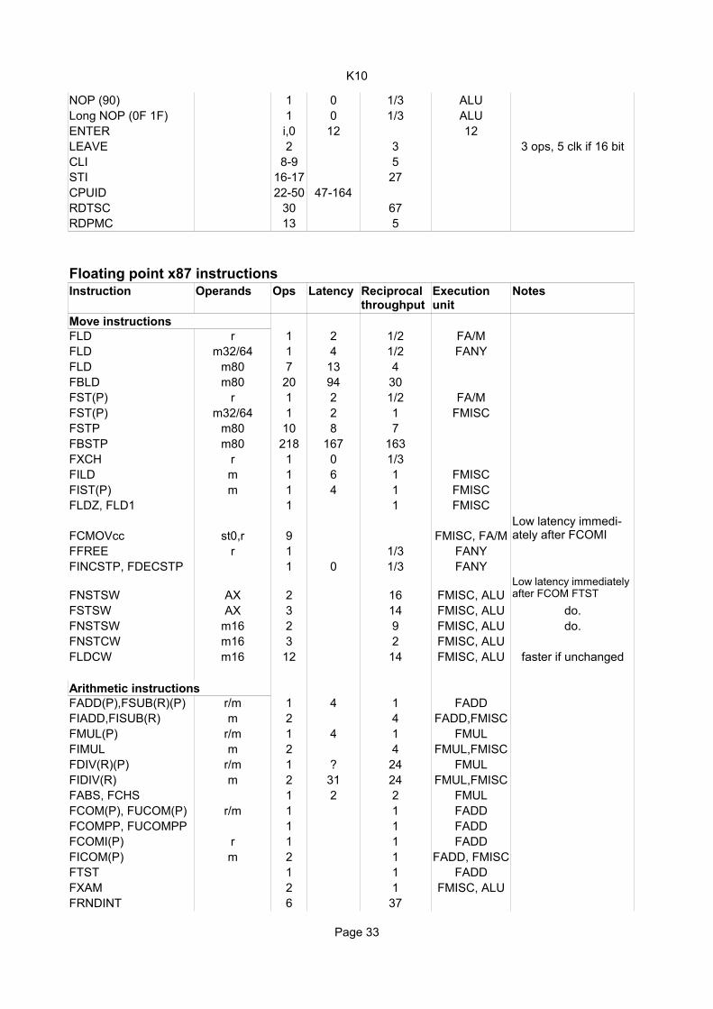
Floating point x87 instructionsInstruction Operands Ops Latency Notes
Move instructionsFLD r 1 2 1/2 FA/MFLD m32/64 1 4 1/2 FANYFLD m80 7 13 4FBLD m80 20 94 30FST(P) r 1 2 1/2 FA/MFST(P) m32/64 1 2 1 FMISCFSTP m80 10 8 7FBSTP m80 218 167 163FXCH r 1 0 1/3FILD m 1 6 1 FMISCFIST(P) m 1 4 1 FMISCFLDZ, FLD1 1 1 FMISC
FCMOVcc st0,r 9 FMISC, FA/MFFREE r 1 1/3 FANYFINCSTP, FDECSTP 1 0 1/3 FANY
FNSTSW AX 2 16 FMISC, ALUFSTSW AX 3 14 FMISC, ALU do.FNSTSW m16 2 9 FMISC, ALU do.FNSTCW m16 3 2 FMISC, ALUFLDCW m16 12 14 FMISC, ALU faster if unchanged
Arithmetic instructionsFADD(P),FSUB(R)(P) r/m 1 4 1 FADDFIADD,FISUB(R) m 2 4 FADD,FMISCFMUL(P) r/m 1 4 1 FMULFIMUL m 2 4 FMUL,FMISCFDIV(R)(P) r/m 1 ? 24 FMULFIDIV(R) m 2 31 24 FMUL,FMISCFABS, FCHS 1 2 2 FMULFCOM(P), FUCOM(P) r/m 1 1 FADDFCOMPP, FUCOMPP 1 1 FADDFCOMI(P) r 1 1 FADDFICOM(P) m 2 1 FADD, FMISCFTST 1 1 FADDFXAM 2 1 FMISC, ALUFRNDINT 6 37
Reciprocal throughput
Execution unit
Low latency immedi-ately after FCOMI
Low latency immediately after FCOM FTST

K10
Page 34
FPREM 1 7 FMULFPREM1 1 7 FMUL
MathFSQRT 1 35 35 FMULFLDPI, etc. 1 1 FMISCFSIN 45 ~51?FCOS 51 ~90?FSINCOS 76 ~125?FPTAN 45 ~119FPATAN 9 151? 45?FSCALE 5 9 29FXTRACT 11 9 41F2XM1 8 65 30?FYL2X 8 13 30?FYL2XP1 12 114 44?
OtherFNOP 1 0 1/3 FANY(F)WAIT 1 0 1/3 ALUFNCLEX 8 28 FMISCFNINIT 26 103 FMISCFNSAVE m 77 162 149FRSTOR m 70 133 149FXSAVE m 61 63 58FXRSTOR m 85 89 79
Integer MMX and XMM instructionsInstruction Operands Ops Latency Notes
Move instructionsMOVD r32, mm 1 3 1 FADDMOVD mm, r32 2 6 3MOVD mm,m32 1 4 1/2 FANYMOVD r32, xmm 1 3 1 FADDMOVD xmm, r32 2 6 3MOVD xmm,m32 1 2 1/2MOVD m32,mm/x 1 2 1 FMISC
MOVD (MOVQ) r64,(x)mm 1 3 1 FADDMOVD (MOVQ) mm,r64 2 6 3 do.MOVD (MOVQ) xmm,r64 2 6 3 FMUL, ALU do.MOVQ mm,mm 1 2 1/2 FA/MMOVQ xmm,xmm 1 2,5 1/3 FANYMOVQ mm,m64 1 4 1/2 FANYMOVQ xmm,m64 1 2 1/2 ?MOVQ m64,(x)mm 1 2 1 FMISCMOVDQA xmm,xmm 1 2,5 1/3 FANYMOVDQA xmm,m 1 2 1/2 ?MOVDQA m,xmm 2 2 1 FMUL,FMISCMOVDQU xmm,m 1 2 1/2
Reciprocal throughput
Execution unit
Moves 64 bits.Name of instruction differs

K10
Page 35
MOVDQU m,xmm 3 3 2MOVDQ2Q mm,xmm 1 2 1/3 FANYMOVQ2DQ xmm,mm 1 2 1/3 FANYMOVNTQ m,mm 1 1 FMISCMOVNTDQ m,xmm 2 1 FMUL,FMISC
mm,r/m 1 2 1/2 FA/M
xmm,r/m 1 3 1/2 FA/M
mm,r/m 1 2 1/2 FA/M
xmm,r/m 1 3 1/2 FA/MPUNPCKHQDQ xmm,r/m 1 3 1/2 FA/MPUNPCKLQDQ xmm,r/m 1 3 1/2 FA/MPSHUFD xmm,xmm,i 1 3 1/2 FA/MPSHUFW mm,mm,i 1 2 1/2 FA/MPSHUFL/HW xmm,xmm,i 1 2 1/2 FA/MMASKMOVQ mm,mm 32 13MASKMOVDQU xmm,xmm 64 24PMOVMSKB r32,mm/xmm 1 3 1 FADDPEXTRW r32,(x)mm,i 2 6 1PINSRW (x)mm,r32,i 2 9 3 FA/MINSERTQ xmm,xmm 3 6 2 FA/M SSE4.A, AMD onlyINSERTQ xmm,xmm,i,i 3 6 2 FA/M SSE4.A, AMD onlyEXTRQ xmm,xmm 1 2 1/2 FA/M SSE4.A, AMD onlyEXTRQ xmm,xmm,i,i 1 2 1/2 FA/M SSE4.A, AMD only
Arithmetic instructions
mm/xmm,r/m 1 2 1/2 FA/MPCMPEQ/GT B/W/D mm/xmm,r/m 1 2 1/2 FA/M
mm/xmm,r/m 1 3 1 FMULPMADDWD mm/xmm,r/m 1 3 1 FMULPAVGB/W mm/xmm,r/m 1 2 1/2 FA/MPMIN/MAX SW/UB mm/xmm,r/m 1 2 1/2 FA/MPSADBW mm/xmm,r/m 1 3 1 FADD
Logic
mm/xmm,r/m 1 2 1/2 FA/M
mm,i/mm/m 1 2 1/2 FA/M
x,i/(x)mm 1 3 1/2 FA/MPSLLDQ, PSRLDQ xmm,i 1 3 1/2 FA/M
PACKSSWB/DW PACKUSWB
PACKSSWB/DW PACKUSWB
PUNPCKH/LBW/WD/DQ
PUNPCKH/LBW/WD/DQ
PADDB/W/D/Q PADDSB/W PADDUSB/W PSUBB/W/D/Q PSUBSB/W PSUBUSB/W
PMULLW PMULHW PMULHUW PMULUDQ
PAND PANDN POR PXOR
PSLL/RL W/D/Q PSRAW/D
PSLL/RL W/D/Q PSRAW/D

K10
Page 36
OtherEMMS 1 1/3 FANY
Floating point XMM instructionsInstruction Operands Ops Latency Notes
Move instructionsMOVAPS/D r,r 1 2,5 1/2 FANYMOVAPS/D r,m 1 2 1/2 ?MOVAPS/D m,r 2 2 1 FMUL,FMISCMOVUPS/D r,r 1 2,5 1/2 FANYMOVUPS/D r,m 1 2 1/2 ?MOVUPS/D m,r 3 3 2 FMISCMOVSS/D r,r 1 2 1/2 FA/MMOVSS/D r,m 1 2 1/2 ?MOVSS/D m,r 1 2 1 FMISC
r,r 1 3 1/2 FA/M
r,m 1 4 1/2 FA/M
m,r 1 1 FMISCMOVNTPS/D m,r 2 3 FMUL,FMISCMOVNTSS/D m,r 1 1 FMISC SSE4.A, AMD onlyMOVMSKPS/D r32,r 1 3 1 FADDSHUFPS/D r,r/m,i 1 3 1/2 FA/MUNPCK H/L PS/D r,r/m 1 3 1/2 FA/M
ConversionCVTPS2PD r,r/m 1 2 1 FMISCCVTPD2PS r,r/m 2 7 1CVTSD2SS r,r/m 3 8 2CVTSS2SD r,r/m 3 7 2CVTDQ2PS r,r/m 1 4 1 FMISCCVTDQ2PD r,r/m 1 4 1 FMISCCVT(T)PS2DQ r,r/m 1 4 1 FMISCCVT(T)PD2DQ r,r/m 2 7 1CVTPI2PS xmm,mm 2 7 1CVTPI2PD xmm,mm 1 4 1 FMISCCVT(T)PS2PI mm,xmm 1 4 1 FMISCCVT(T)PD2PI mm,xmm 2 7 1CVTSI2SS xmm,r32 3 14 3CVTSI2SD xmm,r32 3 14 3CVT(T)SD2SI r32,xmm 2 8 1 FADD,FMISCCVT(T)SS2SI r32,xmm 2 8 1 FADD,FMISC
ArithmeticADDSS/D SUBSS/D r,r/m 1 4 1 FADDADDPS/D SUBPS/D r,r/m 1 4 1 FADDMULSS/D r,r/m 1 4 1 FMUL
Reciprocal throughput
Execution unit
MOVHLPS, MOVLHPS
MOVHPS/D, MOVLPS/D
MOVHPS/D, MOVLPS/D

K10
Page 37
MULPS/D r,r/m 1 4 1 FMULDIVSS r,r/m 1 16 13 FMULDIVPS r,r/m 1 18 15 FMULDIVSD r,r/m 1 20 17 FMULDIVPD r,r/m 1 20 17 FMULRCPSS RCPPS r,r/m 1 3 1 FMULMAXSS/D MINSS/D r,r/m 1 2 1 FADDMAXPS/D MINPS/D r,r/m 1 2 1 FADDCMPccSS/D r,r/m 1 2 1 FADDCMPccPS/D r,r/m 1 2 1 FADD
r,r/m 1 1 FADD
Logic
r,r/m 1 2 1/2 FA/M
MathSQRTSS r,r/m 1 19 16 FMULSQRTPS r,r/m 1 21 18 FMULSQRTSD r,r/m 1 27 24 FMULSQRTPD r,r/m 1 27 24 FMULRSQRTSS r,r/m 1 3 1 FMULRSQRTPS r,r/m 1 3 1 FMUL
OtherLDMXCSR m 12 12 10STMXCSR m 3 12 11
Obsolete 3DNow instructionsInstruction Operands Ops Latency Notes
Move and convert instructionsPF2ID mm,mm 1 5 1 FMISCPI2FD mm,mm 1 5 1 FMISCPF2IW mm,mm 1 5 1 FMISC 3DNow extensionPI2FW mm,mm 1 5 1 FMISC 3DNow extensionPSWAPD mm,mm 1 2 1/2 FA/M 3DNow extension
Integer instructionsPAVGUSB mm,mm 1 2 1/2 FA/MPMULHRW mm,mm 1 3 1 FMUL
Floating point instructionsPFADD/SUB/SUBR mm,mm 1 4 1 FADDPFCMPEQ/GE/GT mm,mm 1 2 1 FADDPFMAX/MIN mm,mm 1 2 1 FADDPFMUL mm,mm 1 4 1 FMULPFACC mm,mm 1 4 1 FADDPFNACC, PFPNACC mm,mm 1 4 1 FADD 3DNow extensionPFRCP mm,mm 1 3 1 FMUL
COMISS/D UCOMISS/D
ANDPS/D ANDNPS/D ORPS/D XORPS/D
Reciprocal throughput
Execution unit

K10
Page 38
PFRCPIT1/2 mm,mm 1 4 1 FMULPFRSQRT mm,mm 1 3 1 FMULPFRSQIT1 mm,mm 1 4 1 FMUL
OtherFEMMS mm,mm 1 1/3 FANY
Thank you to Xucheng Tang for doing the measurements on the K10.
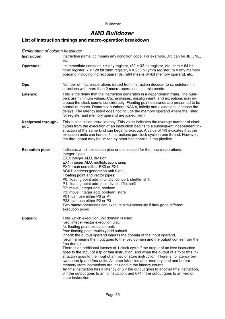
Bulldozer
Page 39
AMD BulldozerList of instruction timings and macro-operation breakdown
Explanation of column headings:Instruction:
Operands:
Ops:
Latency:
Execution pipe:
Domain:
Instruction name. cc means any condition code. For example, Jcc can be JB, JNE, etc.
i = immediate constant, r = any register, r32 = 32-bit register, etc., mm = 64 bit mmx register, x = 128 bit xmm register, y = 256 bit ymm register, m = any memory operand including indirect operands, m64 means 64-bit memory operand, etc.
Number of macro-operations issued from instruction decoder to schedulers. In-structions with more than 2 macro-operations use microcode.
This is the delay that the instruction generates in a dependency chain. The num-bers are minimum values. Cache misses, misalignment, and exceptions may in-crease the clock counts considerably. Floating point operands are presumed to be normal numbers. Denormal numbers, NAN's, infinity and exceptions increase the delays. The latency listed does not include the memory operand where the listing for register and memory operand are joined (r/m).
Reciprocal through-put:
This is also called issue latency. This value indicates the average number of clock cycles from the execution of an instruction begins to a subsequent independent in-struction of the same kind can begin to execute. A value of 1/3 indicates that the execution units can handle 3 instructions per clock cycle in one thread. However, the throughput may be limited by other bottlenecks in the pipeline.
Indicates which execution pipe or unit is used for the macro-operations:Integer pipes:EX0: integer ALU, divisionEX1: integer ALU, multiplication, jumpEX01: can use either EX0 or EX1AG01: address generation unit 0 or 1Floating point and vector pipes:P0: floating point add, mul, div, convert, shuffle, shiftP1: floating point add, mul, div, shuffle, shiftP2: move, integer add, booleanP3: move, integer add, boolean, storeP01: can use either P0 or P1P23: can use either P2 or P3Two macro-operations can execute simultaneously if they go to differentexecution pipes
Tells which execution unit domain is used:ivec: integer vector execution unit.fp: floating point execution unit.fma: floating point multiply/add subunit.inherit: the output operand inherits the domain of the input operand.ivec/fma means the input goes to the ivec domain and the output comes from the fma domain.There is an additional latency of 1 clock cycle if the output of an ivec instruction goes to the input of a fp or fma instruction, and when the output of a fp or fma in-struction goes to the input of an ivec or store instruction. There is no latency be-tween the fp and fma units. All other latencies after memory load and before memory store instructions are included in the latency counts.An fma instruction has a latency of 5 if the output goes to another fma instruction, 6 if the output goes to an fp instuction, and 6+1 if the output goes to an ivec or store instruction.
Bulldozer
Page 40
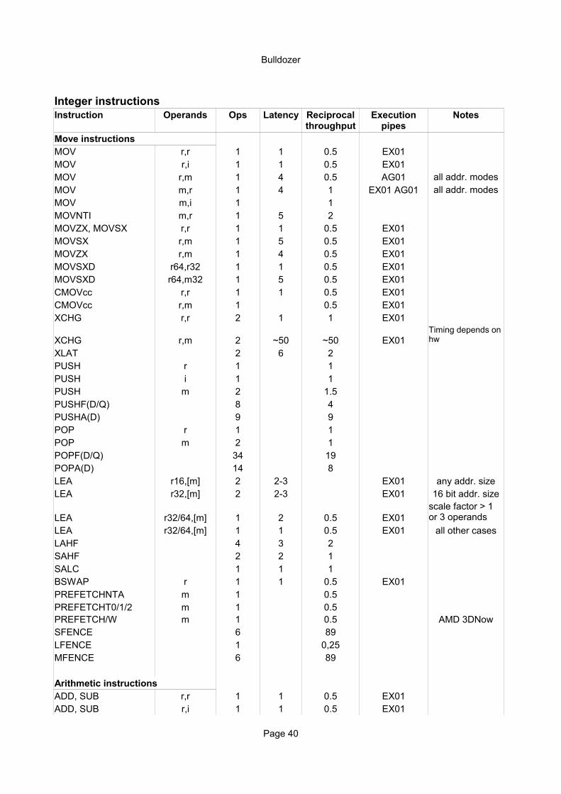
Integer instructionsInstruction Operands Ops Latency Notes
Move instructionsMOV r,r 1 1 0.5 EX01MOV r,i 1 1 0.5 EX01MOV r,m 1 4 0.5 AG01 all addr. modesMOV m,r 1 4 1 EX01 AG01 all addr. modesMOV m,i 1 1MOVNTI m,r 1 5 2MOVZX, MOVSX r,r 1 1 0.5 EX01MOVSX r,m 1 5 0.5 EX01MOVZX r,m 1 4 0.5 EX01MOVSXD r64,r32 1 1 0.5 EX01MOVSXD r64,m32 1 5 0.5 EX01CMOVcc r,r 1 1 0.5 EX01CMOVcc r,m 1 0.5 EX01XCHG r,r 2 1 1 EX01
XCHG r,m 2 ~50 ~50 EX01XLAT 2 6 2PUSH r 1 1PUSH i 1 1PUSH m 2 1.5PUSHF(D/Q) 8 4PUSHA(D) 9 9POP r 1 1POP m 2 1POPF(D/Q) 34 19POPA(D) 14 8LEA r16,[m] 2 2-3 EX01 any addr. sizeLEA r32,[m] 2 2-3 EX01 16 bit addr. size
LEA r32/64,[m] 1 2 0.5 EX01LEA r32/64,[m] 1 1 0.5 EX01 all other casesLAHF 4 3 2SAHF 2 2 1SALC 1 1 1BSWAP r 1 1 0.5 EX01PREFETCHNTA m 1 0.5PREFETCHT0/1/2 m 1 0.5PREFETCH/W m 1 0.5 AMD 3DNowSFENCE 6 89LFENCE 1 0,25MFENCE 6 89
Arithmetic instructionsADD, SUB r,r 1 1 0.5 EX01ADD, SUB r,i 1 1 0.5 EX01
Reciprocal throughput
Execution pipes
Timing depends on hw
scale factor > 1 or 3 operands

Bulldozer
Page 41
ADD, SUB r,m 1 0.5 EX01ADD, SUB m,r 1 7-8 1 EX01ADD, SUB m,i 1 7-8 1 EX01ADC, SBB r,r 1 1 EX01ADC, SBB r,i 1 1 EX01ADC, SBB r,m 1 1 1 EX01ADC, SBB m,r 1 9 1 EX01ADC, SBB m,i 1 9 1 EX01CMP r,r 1 1 0.5 EX01CMP r,i 1 1 0.5 EX01CMP r,m 1 0.5 EX01INC, DEC, NEG r 1 1 0.5 EX01INC, DEC, NEG m 1 7-8 1 EX01AAA, AAS 10 6DAA 16 9DAS 20 10AAD 4 6AAM 9 20 20MUL, IMUL r8/m8 1 4 2 EX1MUL, IMUL r16/m16 2 4 2 EX1MUL, IMUL r32/m32 1 4 2 EX1MUL, IMUL r64/m64 1 6 4 EX1IMUL r16,r16/m16 1 4 2 EX1IMUL r32,r32/m32 1 4 2 EX1IMUL r64,r64/m64 1 6 4 EX1IMUL r16,(r16),i 2 5 2 EX1IMUL r32,(r32),i 1 4 2 EX1IMUL r64,(r64),i 1 6 4 EX1IMUL r16,m16,i 2 2 EX1IMUL r32,m32,i 2 2 EX1IMUL r64,m64,i 2 4 EX1DIV r8/m8 14 20 20 EX0DIV r16/m16 18 15-27 15-28 EX0DIV r32/m32 16 16-43 16-43 EX0DIV r64/m64 16 16-75 16-75 EX0IDIV r8/m8 33 23 20 EX0IDIV r16/m16 36 23-33 20-27 EX0IDIV r32/m32 36 22-48 20-43 EX0IDIV r64/m64 36 22-79 20-75 EX0CBW, CWDE, CDQE 1 1 EX01CDQ, CQO 1 1 0.5 EX01CWD 2 1 1 EX01
Logic instructionsAND, OR, XOR r,r 1 1 0.5 EX01AND, OR, XOR r,i 1 1 0.5 EX01AND, OR, XOR r,m 1 0.5 EX01AND, OR, XOR m,r 1 7-8 1 EX01AND, OR, XOR m,i 1 7-8 1 EX01TEST r,r 1 1 0.5 EX01

Bulldozer
Page 42
TEST r,i 1 1 0.5 EX01TEST m,r 1 0.5 EX01TEST m,i 1 0.5 EX01NOT r 1 1 0.5 EX01NOT m 1 7 1 EX01SHL, SHR, SAR r,i/CL 1 1 0.5 EX01ROL, ROR r,i/CL 1 1 0.5 EX01RCL r,1 1 1 EX01RCL r,i 16 8 EX01RCL r,cl 17 9 EX01RCR r,1 1 1 EX01RCR r,i 15 8 EX01RCR r,cl 16 8 EX01SHLD, SHRD r,r,i 6 3 3 EX01SHLD, SHRD r,r,cl 7 4 3,5 EX01SHLD, SHRD m,r,i/CL 8 3,5 EX01BT r,r/i 1 1 0.5 EX01BT m,i 1 0.5 EX01BT m,r 7 3,5 EX01BTC, BTR, BTS r,r/i 2 2 1 EX01BTC, BTR, BTS m,i 4 2 EX01BTC, BTR, BTS m,r 10 5 EX01BSF r,r 6 3 3 EX01BSF r,m 8 4 4 EX01BSR r,r 7 4 4 EX01BSR r,m 9 5 EX01LZCNT r,r 1 2 2 EX0 SSE4.APOPCNT r,r/m 1 4 2 EX1 SSE4.2SETcc r 1 1 0.5 EX01SETcc m 1 1 EX01CLC, STC 1 0.5 EX01CMC 1 1 EX01CLD 2 3STD 2 4POPCNT r16/32,r16/32 1 4 2 SSE4APOPCNT r64,r64 1 4 4 SSE4ALZCNT r,r 2 2 2 SSE4AEXTRQ x,i,i 1 3 1 P1 SSE4AEXTRQ x,x 1 3 1 P1 SSE4AINSERTQ x,x,i,i 1 3 1 P1 SSE4AINSERTQ x,x 1 3 1 P1 SSE4A
Control transfer instructionsJMP short/near 1 2 EX1JMP r 1 2 EX1JMP m 1 2 EX1Jcc short/near 1 1-2 EX1 2 if jumpingfused CMP+Jcc short/near 1 1-2 EX1 2 if jumpingJ(E/R)CXZ short 1 1-2 EX1 2 if jumpingLOOP short 1 1-2 EX1 2 if jumpingLOOPE LOOPNE short 1 1-2 EX1 2 if jumping

Bulldozer
Page 43
CALL near 2 2 EX1CALL r 2 2 EX1CALL m 3 2 EX1RET 1 2 EX1RET i 4 2-3 EX1BOUND m 11 5 for no jumpINTO 4 24 for no jump
String instructionsLODS 3 3REP LODS 6n 3nSTOS 3 3REP STOS 2n 2n small nREP STOS 3 per 16B 3 per 16B best caseMOVS 5 3REP MOVS 2n 2n small nREP MOVS 4 per 16B 3 per 16B best caseSCAS 3 3REP SCAS 7n 4nCMPS 6 3REP CMPS 9n 4n
SynchronizationLOCK ADD m,r 1 ~55XADD m,r 4 10LOCK XADD m,r 4 ~51CMPXCHG m8,r8 5 15LOCK CMPXCHG m8,r8 5 ~51CMPXCHG m,r16/32/64 6 14LOCK CMPXCHG m,r16/32/64 6 ~52CMPXCHG8B m64 18 15LOCK CMPXCHG8B m64 18 ~53CMPXCHG16B m128 22 52LOCK CMPXCHG16B m128 22 ~94
OtherNOP (90) 1 0.25 noneLong NOP (0F 1F) 1 0.25 nonePAUSE 40 43ENTER a,0 13 22ENTER a,b 11+5b 16+4bLEAVE 2 4CPUID 37-63 112-280RDTSC 36 42RDPMC 22 300CRC32 r32,r8 3 3 2CRC32 r32,r16 5 5 5CRC32 r32,r32 5 6 6XGETBV 4 31
Bulldozer
Page 44
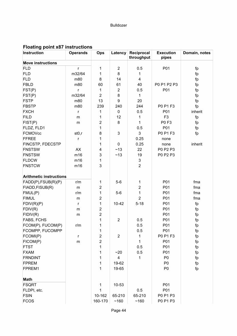
Floating point x87 instructionsInstruction Operands Ops Latency Domain, notes
Move instructionsFLD r 1 2 0.5 P01 fpFLD m32/64 1 8 1 fpFLD m80 8 14 4 fpFBLD m80 60 61 40 P0 P1 P2 P3 fpFST(P) r 1 2 0.5 P01 fpFST(P) m32/64 2 8 1 fpFSTP m80 13 9 20 fpFBSTP m80 239 240 244 P0 P1 F3 fpFXCH r 1 0 0.5 P01 inheritFILD m 1 12 1 F3 fpFIST(P) m 2 8 1 P0 F3 fpFLDZ, FLD1 1 0.5 P01 fpFCMOVcc st0,r 8 3 3 P0 P1 F3 fpFFREE r 1 0.25 noneFINCSTP, FDECSTP 1 0 0.25 none inheritFNSTSW AX 4 ~13 22 P0 P2 P3FNSTSW m16 3 ~13 19 P0 P2 P3FLDCW m16 1 3FNSTCW m16 3 2
Arithmetic instructionsFADD(P),FSUB(R)(P) r/m 1 5-6 1 P01 fmaFIADD,FISUB(R) m 2 2 P01 fmaFMUL(P) r/m 1 5-6 1 P01 fmaFIMUL m 2 2 P01 fmaFDIV(R)(P) r 1 10-42 5-18 P01 fpFDIV(R) m 2 P01 fpFIDIV(R) m 2 P01 fpFABS, FCHS 1 2 0.5 P01 fpFCOM(P), FUCOM(P) r/m 1 0.5 P01 fpFCOMPP, FUCOMPP 1 0.5 P01 fpFCOMI(P) r 2 2 1 P0 P1 F3 fpFICOM(P) m 2 1 P01 fpFTST 1 0.5 P01 fpFXAM 1 ~20 0.5 P01 fpFRNDINT 1 4 1 P0 fpFPREM 1 19-62 P0 fpFPREM1 1 19-65 P0 fp
MathFSQRT 1 10-53 P01FLDPI, etc. 1 0.5 P01FSIN 10-162 65-210 65-210 P0 P1 P3FCOS 160-170 ~160 ~160 P0 P1 P3
Reciprocal throughput
Execution pipes

Bulldozer
Page 45
FSINCOS 12-166 95-160 95-160 P0 P1 P3FPTAN 11-190 95-245 95-245 P0 P1 P3FPATAN 10-355 60-440 60-440 P0 P1 P3FSCALE 8 52 P0 P1 P3FXTRACT 12 10 5 P0 P1 P3F2XM1 10 64-71 P0 P1 P3FYL2X 10-175 P0 P1 P3FYL2XP1 10-175 P0 P1 P3
OtherFNOP 1 0.25 none(F)WAIT 1 0.25 noneFNCLEX 18 57 P0FNINIT 31 170 P0FNSAVE m864 103 300 300 P0 P1 P2 P3FRSTOR m864 76 312 312 P0 P3
Integer vector instructionsInstruction Operands Ops Latency Notes
Move instructionsMOVD r32/64, mm/x 1 8 1MOVD mm/x, r32/64 2 10 1MOVD mm/x,m32 1 6 0.5MOVD m32,mm/x 1 5 1MOVQ mm/x,mm/x 1 2 0.5 P23MOVQ mm/x,m64 1 6 0.5MOVQ m64,mm/x 1 5 1 P3MOVDQA xmm,xmm 1 0 0.25 none inherit domainMOVDQA xmm,m 1 6 0.5MOVDQA m,xmm 1 5 1 P3VMOVDQA ymm,ymm 2 2 0.5 P23VMOVDQA ymm,m256 2 6 1VMOVDQA m256,ymm 4 5 3 P3MOVDQU xmm,xmm 1 0 0.25 none inherit domainMOVDQU xmm,m 1 6 0.5MOVDQU m,xmm 1 5 1 P3LDDQU xmm,m 1 6 0.5VMOVDQU ymm,m256 2 6 1-2VMOVDQU m256,ymm 8 6 10 P2 P3MOVDQ2Q mm,xmm 1 2 0.5 P23MOVQ2DQ xmm,mm 1 2 0.5 P23MOVNTQ m,mm 1 6 2 P3MOVNTDQ m,xmm 1 6 2 P3MOVNTDQA xmm,m 1 6 0.5PACKSSWB/DW (x)mm,r/m 1 2 1 P1PACKUSWB (x)mm,r/m 1 2 1 P1
(x)mm,r/m 1 2 1 P1
Reciprocal throughput
Execution pipes
PUNPCKH/LBW/WD/DQ

Bulldozer
Page 46
PUNPCKHQDQ xmm,r/m 1 2 1 P1PUNPCKLQDQ xmm,r/m 1 2 1 P1PSHUFB (x)mm,r/m 1 3 1 P1PSHUFD xmm,xmm,i 1 2 1 P1PSHUFW mm,mm,i 1 2 1 P1PSHUFL/HW xmm,xmm,i 1 2 1 P1PALIGNR (x)mm,r/m,i 1 2 1 P1PBLENDW xmm,r/m 1 2 0.5 P23 SSE4.1MASKMOVQ mm,mm 31 38 37 P3MASKMOVDQU xmm,xmm 64 48 61 P1 P3PMOVMSKB r32,mm/x 2 10 1 P1 P3PEXTRB/W/D/Q r,x/mm,i 2 10 1 P1 P3 AVXPINSRB/W/D/Q x/mm,r,i 2 12 2 P1
xmm,xmm 1 2 1 P1 SSE4.1
xmm,xmm 1 2 1 P1 SSE4.1VPCMOV x,x,x,x/m 1 2 1 P1 AMD XOPVPCMOV y,y,y,y/m 2 2 2 P1 AMD XOPVPPERM x,x,x,x/m 1 2 1 P1 AMD XOP
Arithmetic instructions
(x)mm,r/m 1 2 0.5 P23
(x)mm,r/m 1 2 0.5 P23PHADD/SUB(S)W/D x,x 3 5 2 P1 P23 SSSE3PHADD/SUB(S)W/D x,m 4 5 2 P1 P23 SSSE3PCMPEQ/GT B/W/D (x)mm,r/m 1 2 0.5 P23PCMPEQQ (x)mm,r/m 1 2 0.5 P23 SSE4.1PCMPGTQ (x)mm,r/m 1 2 0.5 P23 SSE4.2
(x)mm,r/m 1 4 1 P0PMULLD xmm,r/m 1 5 2 P0 SSE4.1PMULDQ xmm,r/m 1 4 1 P0 SSE4.1PMULHRSW (x)mm,r/m 1 4 1 P0 SSSE3PMADDWD (x)mm,r/m 1 4 1 P0PMADDUBSW (x)mm,r/m 1 4 1 P0PAVGB/W (x)mm,r/m 1 2 0.5 P23
(x)mm,r/m 1 2 0.5 P23PHMINPOSUW xmm,r/m 2 4 1 P1 P23 SSE4.1PABSB/W/D (x)mm,r/m 1 2 0.5 P23 SSSE3PSIGNB/W/D (x)mm,r/m 1 2 0.5 P23 SSSE3PSADBW (x)mm,r/m 2 4 1 P23MPSADBW x,x,i 8 8 4 P1 P23 SSE4.1
VPCOMB/W/D/Q x,x,x/m,i 1 2 0.5 P23
VPCOMUB/W/D/Q x,x,x/m,i 1 2 0.5 P23
PMOVSXBW/BD/BQ/WD/WQ/DQ
PMOVZXBW/BD/BQ/WD/WQ/DQ
PADDB/W/D/Q/SB/SW/USB/USW
PSUBB/W/D/Q/SB/SW/USB/USW
PMULLW PMULHW PMULHUW PMULUDQ
PMIN/MAX SB/SW/ SD UB/UW/UD
AMD XOPlatency 0 if i=6,7
AMD XOPlatency 0 if i=6,7

Bulldozer
Page 47
x,x/m 1 2 0.5 P23 AMD XOP
x,x/m 1 2 0.5 P23 AMD XOPVPHSUBBW/WD/DQ x,x/m 1 2 0.5 P23 AMD XOPVPMACSWW/WD x,x,x/m,x 1 4 1 P0 AMD XOPVPMACSDD x,x,x/m,x 1 5 2 P0 AMD XOPVPMACSDQH/L x,x,x/m,x 1 4 1 P0 AMD XOPVPMACSSWW/WD x,x,x/m,x 1 4 1 P0 AMD XOPVPMACSSDD x,x,x/m,x 1 5 2 P0 AMD XOPVPMACSSDQH/L x,x,x/m,x 1 4 1 P0 AMD XOPVPMADCSWD x,x,x/m,x 1 4 1 P0 AMD XOPVPMADCSSWD x,x,x/m,x 1 4 1 P0 AMD XOP
Logic
(x)mm,r/m 1 2 0.5 P23
(x)mm,r/m 1 3 1 P1
(x)mm,i 1 2 1 P1PSLLDQ, PSRLDQ xmm,i 1 2 1 P1PTEST xmm,r/m 2 1 P1 P3 SSE4.1VPROTB/W/D/Q x,x,x/m 1 3 1 P1 AMD XOPVPROTB/W/D/Q x,x,i 1 2 1 P1 AMD XOPVPSHAB/W/D/Q x,x,x/m 1 3 1 P1 AMD XOPVPSHLB/W/D/Q x,x,x/m 1 3 1 P1 AMD XOP
String instructionsPCMPESTRI x,x,i 27 17 10 P1 P2 P3 SSE4.2PCMPESTRM x,x,i 27 10 10 P1 P2 P3 SSE4.2PCMPISTRI x,x,i 7 14 3 P1 P2 P3 SSE4.2PCMPISTRM x,x,i 7 7 4 P1 P2 P3 SSE4.2
EncryptionPCLMULQDQ x,x/m,i 5 12 7 P1 pclmulAESDEC x,x 2 5 2 P01 aesAESDECLAST x,x 2 5 2 P01 aesAESENC x,x 2 5 2 P01 aesAESENCLAST x,x 2 5 2 P01 aesAESIMC x,x 1 5 1 P0 aesAESKEYGENASSIST x,x,i 1 5 1 P0 aes
OtherEMMS 1 0.25
Floating point XMM and YMM instructionsInstruction Operands Ops Latency Domain, notes
Move instructions
VPHADDBW/BD/BQ/ WD/WQ/DQ
VPHADDUBW/BD/BQ/WD/WQ/DQ
PAND PANDN POR PXOR
PSLL/RL W/D/Q PSRAW/D
PSLL/RL W/D/Q PSRAW/D
Reciprocal throughput
Execution pipes
Bulldozer
Page 48
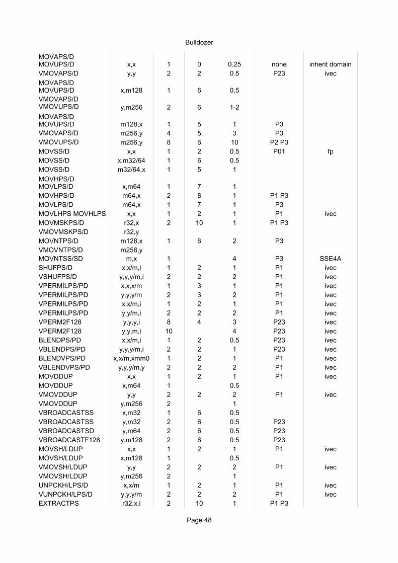
x,x 1 0 0.25 none inherit domainVMOVAPS/D y,y 2 2 0.5 P23 ivec
x,m128 1 6 0.5
y,m256 2 6 1-2
m128,x 1 5 1 P3VMOVAPS/D m256,y 4 5 3 P3VMOVUPS/D m256,y 8 6 10 P2 P3MOVSS/D x,x 1 2 0.5 P01 fpMOVSS/D x,m32/64 1 6 0.5MOVSS/D m32/64,x 1 5 1
x,m64 1 7 1MOVHPS/D m64,x 2 8 1 P1 P3MOVLPS/D m64,x 1 7 1 P3MOVLHPS MOVHLPS x,x 1 2 1 P1 ivecMOVMSKPS/D r32,x 2 10 1 P1 P3VMOVMSKPS/D r32,yMOVNTPS/D m128,x 1 6 2 P3VMOVNTPS/D m256,yMOVNTSS/SD m,x 1 4 P3 SSE4ASHUFPS/D x,x/m,i 1 2 1 P1 ivecVSHUFPS/D y,y,y/m,i 2 2 2 P1 ivecVPERMILPS/PD x,x,x/m 1 3 1 P1 ivecVPERMILPS/PD y,y,y/m 2 3 2 P1 ivecVPERMILPS/PD x,x/m,i 1 2 1 P1 ivecVPERMILPS/PD y,y/m,i 2 2 2 P1 ivecVPERM2F128 y,y,y,i 8 4 3 P23 ivecVPERM2F128 y,y,m,i 10 4 P23 ivecBLENDPS/PD x,x/m,i 1 2 0.5 P23 ivecVBLENDPS/PD y,y,y/m,i 2 2 1 P23 ivecBLENDVPS/PD x,x/m,xmm0 1 2 1 P1 ivecVBLENDVPS/PD y,y,y/m,y 2 2 2 P1 ivecMOVDDUP x,x 1 2 1 P1 ivecMOVDDUP x,m64 1 0.5VMOVDDUP y,y 2 2 2 P1 ivecVMOVDDUP y,m256 2 1VBROADCASTSS x,m32 1 6 0.5VBROADCASTSS y,m32 2 6 0.5 P23VBROADCASTSD y,m64 2 6 0.5 P23VBROADCASTF128 y,m128 2 6 0.5 P23MOVSH/LDUP x,x 1 2 1 P1 ivecMOVSH/LDUP x,m128 1 0.5VMOVSH/LDUP y,y 2 2 2 P1 ivecVMOVSH/LDUP y,m256 2 1UNPCKH/LPS/D x,x/m 1 2 1 P1 ivecVUNPCKH/LPS/D y,y,y/m 2 2 2 P1 ivecEXTRACTPS r32,x,i 2 10 1 P1 P3
MOVAPS/D MOVUPS/D
MOVAPS/D MOVUPS/DVMOVAPS/D VMOVUPS/D
MOVAPS/D MOVUPS/D
MOVHPS/D MOVLPS/D

Bulldozer
Page 49
EXTRACTPS m32,x,i 2 14 1 P1 P3VEXTRACTF128 x,y,i 1 2 1 P23 ivecVEXTRACTF128 m128,y,i 2 7 1 P23INSERTPS x,x,i 1 2 1 P1INSERTPS x,m32,i 1 1 P1VINSERTF128 y,y,x,i 2 2 1 P23 ivecVINSERTF128 y,y,m128,i 2 9 1 P23VMASKMOVPS/D x,x,m128 1 9 0.5 P01VMASKMOVPS/D y,y,m256 2 9 1 P01VMASKMOVPS/D m128,x,x 18 22 7 P0 P1 P2 P3VMASKMOVPS/D m256,y,y 34 25 13 P0 P1 P2 P3
ConversionCVTPD2PS x,x 2 7 1 P01 fpVCVTPD2PS x,y 4 7 2 P01 fpCVTPS2PD x,x 2 7 1 P01 fpVCVTPS2PD y,x 4 7 2 P01 fpCVTSD2SS x,x 1 4 1 P0 fpCVTSS2SD x,x 1 4 1 P0 fpCVTDQ2PS x,x 1 4 1 P0 fpVCVTDQ2PS y,y 2 4 2 P0 fpCVT(T) PS2DQ x,x 1 4 1 P0 fpVCVT(T) PS2DQ y,y 2 4 2 P0 fpCVTDQ2PD x,x 2 7 1 P01 fpVCVTDQ2PD y,x 4 8 2 P01 fpCVT(T)PD2DQ x,x 2 7 1 P01 fpVCVT(T)PD2DQ x,y 4 7 2 P01 fpCVTPI2PS x,mm 1 4 1 P0 fpCVT(T)PS2PI mm,x 1 4 1 P0 fpCVTPI2PD x,mm 2 7 1 P0 P1 fpCVT(T) PD2PI mm,x 2 7 1 P0 P1 fpCVTSI2SS x,r32 2 14 1 P0 fpCVT(T)SS2SI r32,x 2 13 1 P0 fpCVTSI2SD x,r32/64 2 14 1 P0 fpCVT(T)SD2SI r32/64,x 2 13 1 P0 fp
ArithmeticADDSS/D SUBSS/D x,x/m 1 5-6 0.5 P01 fmaADDPS/D SUBPS/D x,x/m 1 5-6 0.5 P01 fma
VADDPS/D VSUBPS/D y,y,y/m 2 5-6 1 P01 fmaADDSUBPS/D x,x/m 1 5-6 0.5 P01 fmaVADDSUBPS/D y,y,y/m 2 5-6 1 P01 fma
HADDPS/D HSUBPS/D x,x 3 10 2 P01 P1 ivec/fma
HADDPS/D HSUBPS/D x,m128 4 2 P01 P1 ivec/fma
y,y,y 8 10 4 P01 P1 ivec/fma
y,y,m 10 4 P01 P1 ivec/fma
VHADDPS/DVHSUBPS/D
VHADDPS/DVHSUBPS/D

Bulldozer
Page 50
MULSS MULSD x,x/m 1 5-6 0.5 P01 fmaMULPS MULPD x,x/m 1 5-6 0.5 P01 fmaVMULPS VMULPD y,y,y/m 2 5-6 1 P01 fmaDIVSS DIVPS x,x/m 1 9-24 4.5-9.5 P01 fpVDIVPS y,y,y/m 2 9-24 9-19 P01 fpDIVSD DIVPD x,x/m 1 9-27 4.5-11 P01 fpVDIVPD y,y,y/m 2 9-27 9-22 P01 fpRCPSS/PS x,x/m 1 5 1 P01 fpVRCPPS y,y/m 2 5 2 P01 fp
x,x/m 1 2 0.5 P01 fpVCMPPS/D y,y,y/m 2 2 1 P01 fp
x,x/m 2 1 P01 P3 fp
x,x/m 1 2 0.5 P01 fp
VMAXPS/D VMINPS/D y,y,y/m 2 2 1 P01 fpROUNDSS/SD/PS/PD x,x/m,i 1 4 1 P0 fp
y,y/m,i 2 4 2 P0 fpDPPS x,x,i 16 25 6 P01 P23 fmaDPPS x,m128,i 18 7 P01 P23 fmaVDPPS y,y,y,i 25 27 13 P01 P3 fmaVDPPS y,m256,i 29 13 P01 P3 fmaDPPD x,x,i 15 15 5 P01 P23 fmaDPPD x,m128,i 17 6 P01 P23 fmaVFMADDSS/SD x,x,x,x/m 1 5-6 0.5 P01 AMD FMA4VFMADDPS/PD x,x,x,x/m 1 5-6 0.5 P01 AMD FMA4VFMADDPS/PD y,y,y,y/m 2 5-6 1 P01 AMD FMA4All other FMA4 instructions: same as above AMD FMA4
MathSQRTSS/PS x,x/m 1 14-15 4.5-12 P01 fpVSQRTPS y,y/m 2 14-15 9-24 P01 fpSQRTSD/PD x,x/m 1 24-26 4.5-16.5 P01 fpVSQRTPD y,y/m 2 24-26 9-33 P01 fpRSQRTSS/PS x,x/m 1 5 1 P01 fpVRSQRTPS y,y/m 2 5 2 P01 fpVFRCZSS/SD/PS/PD x,x 2 10 2 P01 AMD XOPVFRCZSS/SD/PS/PD x,m 3 10 2 P01 AMD XOP
Logic
x,x/m 1 2 0.5 P23 ivec
y,y,y/m 2 2 1 P23 ivec
OtherVZEROUPPER 9 4 32 bit modeVZEROUPPER 16 5 64 bit mode
CMPSS/DCMPPS/D
COMISS/D UCOMISS/D
MAXSS/SD/PS/PD MINSS/SD/PS/PD
VROUNDSS/SD/PS/ PD
AND/ANDN/OR/XORPS/ PD
VAND/ANDN/OR/XORPS/PD

Bulldozer
Page 51
VZEROALL 17 6 P2 P3 32 bit modeVZEROALL 32 10 P2 P3 64 bit modeLDMXCSR m32 1 10 4 P0 P3STMXCSR m32 2 19 19 P0 P3FXSAVE m4096 67 136 136 P0 P1 P2 P3FXRSTOR m4096 116 176 176 P0 P1 P2 P3XSAVE m 122 196 196 P0 P1 P2 P3XRSTOR m 177 250 250 P0 P1 P2 P3

Piledriver
Page 52
AMD PiledriverList of instruction timings and macro-operation breakdown
Explanation of column headings:Instruction:
Operands:
Ops:
Latency:
Execution pipe:
Domain:
Instruction name. cc means any condition code. For example, Jcc can be JB, JNE, etc.
i = immediate constant, r = any register, r32 = 32-bit register, etc., mm = 64 bit mmx register, x = 128 bit xmm register, y = 256 bit ymm register, m = any memory operand including indirect operands, m64 means 64-bit memory operand, etc.
Number of macro-operations issued from instruction decoder to schedulers. In-structions with more than 2 macro-operations use microcode.
This is the delay that the instruction generates in a dependency chain. The num-bers are minimum values. Cache misses, misalignment, and exceptions may in-crease the clock counts considerably. Floating point operands are presumed to be normal numbers. Denormal numbers, NAN's, infinity and exceptions increase the delays. The latency listed does not include the memory operand where the listing for register and memory operand are joined (r/m).
Reciprocal through-put:
This is also called issue latency. This value indicates the average number of clock cycles from the execution of an instruction begins to a subsequent independent in-struction of the same kind can begin to execute. A value of 1/3 indicates that the execution units can handle 3 instructions per clock cycle in one thread. However, the throughput may be limited by other bottlenecks in the pipeline.
Indicates which execution pipe or unit is used for the macro-operations:Integer pipes:EX0: integer ALU, divisionEX1: integer ALU, multiplication, jumpEX01: can use either EX0 or EX1AG01: address generation unit 0 or 1Floating point and vector pipes:P0: floating point add, mul, div, convert, shuffle, shiftP1: floating point add, mul, div, shuffle, shiftP2: move, integer add, booleanP3: move, integer add, boolean, storeP01: can use either P0 or P1P23: can use either P2 or P3Two macro-operations can execute simultaneously if they go to differentexecution pipes
Tells which execution unit domain is used:ivec: integer vector execution unit.fp: floating point execution unit.fma: floating point multiply/add subunit.inherit: the output operand inherits the domain of the input operand.ivec/fma means the input goes to the ivec domain and the output comes from the fma domain.There is an additional latency of 1 clock cycle if the output of an ivec instruction goes to the input of a fp or fma instruction, and when the output of a fp or fma in-struction goes to the input of an ivec or store instruction. There is no latency be-tween the fp and fma units. All other latencies after memory load and before memory store instructions are included in the latency counts.An fma instruction has a latency of 5 if the output goes to another fma instruction, 6 if the output goes to an fp instuction, and 6+1 if the output goes to an ivec or store instruction.

Piledriver
Page 53
Integer instructionsInstruction Operands Ops Latency Notes
Move instructionsMOV r8,r8 1 1 0.5 EX01MOV r16,r16 1 1 0.5 EX01MOV r32,r32 1 1 0.3 EX01 or AG01MOV r64,r64 1 1 0.3 EX01 or AG01MOV r,i 1 1 0.5 EX01MOV r,m 1 4 0.5 AG01 all addr. modesMOV m,r 1 4 1 EX01 AG01 all addr. modesMOV m,i 1 1MOVNTI m,r 1 4 2MOVZX, MOVSX r16,r8 1 1 1 EX01MOVZX, MOVSX r32,r 1 1 0.5 EX01MOVZX, MOVSX r64,r 1 1 0.5 EX01MOVSX r,m 1 5 0.5 EX01MOVZX r,m 1 4 0.5 EX01MOVSXD r64,r32 1 1 0.5 EX01MOVSXD r64,m32 1 5 0.5 EX01CMOVcc r,r 1 1 0.5 EX01CMOVcc r,m 1 0.5 EX01XCHG r8,r8 2 1 1 EX01XCHG r16,r16 2 1 1 EX01XCHG r32,r32 2 1 0.5 EX01XCHG r64,r64 2 1 0.5 EX01
XCHG r,m 2 ~40 ~40 EX01XLAT 2 6 2PUSH r 1 1PUSH i 1 1PUSH m 2 1PUSHF(D/Q) 8 4PUSHA(D) 9 9POP r 1 1POP m 2 1POPF(D/Q) 34 18POPA(D) 14 8LEA r16,[m] 2 2-3 EX01 any addr. sizeLEA r32,[m] 2 2-3 EX01 16 bit addr. size
LEA r32/64,[m] 1 2 0.5 EX01LEA r32/64,[m] 1 1 0.5 EX01 all other casesLAHF 4 3 2SAHF 2 2 1SALC 1 1 1BSWAP r 1 1 0.5 EX01PREFETCHNTA m 1 0.5PREFETCHT0/1/2 m 1 0.5PREFETCH/W m 1 0.5 PREFETCHWSFENCE 7 81
Reciprocal throughput
Execution pipes
Timing depends on hw
scale factor > 1 or 3 operands

Piledriver
Page 54
LFENCE 1 0,25MFENCE 7 81
Arithmetic instructionsADD, SUB r,r 1 1 0.5 EX01ADD, SUB r,i 1 1 0.5 EX01ADD, SUB r,m 1 0.5 EX01ADD, SUB m,r 1 7-8 1 EX01ADD, SUB m,i 1 7-8 1 EX01ADC, SBB r,r 1 1 EX01ADC, SBB r,i 1 1 EX01ADC, SBB r,m 1 1 1 EX01ADC, SBB m,r 1 9 1 EX01ADC, SBB m,i 1 9 1 EX01CMP r,r 1 1 0.5 EX01CMP r,i 1 1 0.5 EX01CMP r,m 1 0.5 EX01CMP m,i 1 0.5 EX01INC, DEC, NEG r 1 1 0.5 EX01INC, DEC, NEG m 1 7-8 1 EX01AAA, AAS 10 6DAA 16 9DAS 20 10AAD 4 6AAM 10 15 15MUL, IMUL r8/m8 1 4 2 EX1MUL, IMUL r16/m16 2 4 2 EX1MUL, IMUL r32/m32 1 4 2 EX1MUL, IMUL r64/m64 1 6 4 EX1IMUL r16,r16/m16 1 4 2 EX1IMUL r32,r32/m32 1 4 2 EX1IMUL r64,r64/m64 1 6 4 EX1IMUL r16,(r16),i 2 5 2 EX1IMUL r32,(r32),i 1 4 2 EX1IMUL r64,(r64),i 1 6 4 EX1IMUL r16,m16,i 2 2 EX1IMUL r32,m32,i 2 2 EX1IMUL r64,m64,i 2 4 EX1DIV r8/m8 9 17-22 13-22 EX0DIV r16/m16 7 13-26 13-25 EX0DIV r32/m32 2 12-40 12-40 EX0DIV r64/m64 2 13-71 13-71 EX0IDIV r8/m8 9 17-21 13-18 EX0IDIV r16/m16 7 13-26 13-25 EX0IDIV r32/m32 2 13-40 13-40 EX0IDIV r64/m64 2 13-71 13-71 EX0CBW, CWDE, CDQE 1 1 EX01CDQ, CQO 1 1 0.5 EX01CWD 2 1 1 EX01
Logic instructionsAND, OR, XOR r,r 1 1 0.5 EX01AND, OR, XOR r,i 1 1 0.5 EX01

Piledriver
Page 55
AND, OR, XOR r,m 1 0.5 EX01AND, OR, XOR m,r 1 7-8 1 EX01AND, OR, XOR m,i 1 7-8 1 EX01TEST r,r 1 1 0.5 EX01TEST r,i 1 1 0.5 EX01TEST m,r 1 0.5 EX01TEST m,i 1 0.5 EX01NOT r 1 1 0.5 EX01NOT m 1 7-8 1 EX01ANDN r,r,r 1 1 0.5 EX01 BMI1SHL, SHR, SAR r,i/CL 1 1 0.5 EX01ROL, ROR r,i/CL 1 1 0.5 EX01RCL r,1 1 1 EX01RCL r,i 16 7 EX01RCL r,cl 17 7 EX01RCR r,1 1 1 EX01RCR r,i 15 7 EX01RCR r,cl 16 6 EX01SHLD, SHRD r,r,i 6 3 3 EX01SHLD, SHRD r,r,cl 7 3 3 EX01SHLD, SHRD m,r,i/CL 8 3,5 EX01BT r,r/i 1 1 0.5 EX01BT m,i 1 0.5 EX01BT m,r 7 3,5 EX01BTC, BTR, BTS r,r/i 2 2 1 EX01BTC, BTR, BTS m,i 4 20 EX01BTC, BTR, BTS m,r 10 21 EX01BSF r,r 6 3 3 EX01BSF r,m 8 4 4 EX01BSR r,r 7 4 4 EX01BSR r,m 9 5 EX01SETcc r 1 1 0.5 EX01SETcc m 1 1 EX01CLC, STC 1 0.5 EX01CMC 1 1 EX01CLD 2 3STD 2 4POPCNT r16/32,r16/32 1 4 2 SSE4.2POPCNT r64,r64 1 4 4 SSE4.2LZCNT r,r 1 2 2 EX0 LZCNTTZCNT r,r 2 2 2 BMI1BEXTR r,r,r 2 2 0.67 BMI1BEXTR r,r,i 2 2 0.67 AMD TBMBLSI r,r 2 2 1 BMI1BLSMSK r,r 2 2 1 BMI1BLSR r,r 2 2 1 BMI1BLCFILL r,r 2 2 1 AMD TBMBLCI r,r 2 2 1 AMD TBMBLCIC r,r 2 2 1 AMD TBMBLCMSK r,r 2 2 1 AMD TBMBLCS r,r 2 2 1 AMD TBMBLSFILL r,r 2 2 1 AMD TBMBLSI r,r 2 2 1 AMD TBM

Piledriver
Page 56
BLSIC r,r 2 2 1 AMD TBMT1MSKC r,r 2 2 1 AMD TBMTZMSK r,r 2 2 1 AMD TBM
Control transfer instructionsJMP short/near 1 2 EX1JMP r 1 2 EX1JMP m 1 2 EX1Jcc short/near 1 1-2 EX1 2 if jumpingfused CMP+Jcc short/near 1 1-2 EX1 2 if jumpingJ(E/R)CXZ short 1 1-2 EX1 2 if jumpingLOOP short 1 1-2 EX1 2 if jumpingLOOPE LOOPNE short 1 1-2 EX1 2 if jumpingCALL near 2 2 EX1CALL r 2 2 EX1CALL m 3 2 EX1RET 1 2 EX1RET i 4 2 EX1BOUND m 11 5 for no jumpINTO 4 2 for no jump
String instructionsLODS 3 3REP LODS m8/m16 6n 3nREP LODS m32/m64 6n 2.5nSTOS 3 3REP STOS 1n 1n small nREP STOS 3 per 16B 3 per 16B best caseMOVS 5 3REP MOVS 1-3n 1n small nREP MOVS 4.5 pr 16B 3 per 16B best caseSCAS 3 3REP SCAS 7n 3-4nCMPS 6 3REP CMPS 9n 4n
SynchronizationLOCK ADD m,r 1 ~40XADD m,r 4 20LOCK XADD m,r 4 ~39CMPXCHG m,r8/16 5 23LOCK CMPXCHG m,r8/16 5 ~40CMPXCHG m,r32/64 6 20LOCK CMPXCHG m,r32/64 6 ~40CMPXCHG8B m64 18 25LOCK CMPXCHG8B m64 18 ~42CMPXCHG16B m128 22 66LOCK CMPXCHG16B m128 22 ~80
OtherNOP (90) 1 0.25 noneLong NOP (0F 1F) 1 0.25 nonePAUSE 40 40

Piledriver
Page 57
ENTER a,0 13 21ENTER a,b 20+3b 16+4bLEAVE 2 4CPUID 38-64 105-271XGETBV 4 30RDTSC 36 42RDPMC 21 310CRC32 r32,r8 3 3 2CRC32 r32,r16 5 5 5CRC32 r32,r32 5 6 6
Floating point x87 instructionsInstruction Operands Ops Latency Domain, notes
Move instructionsFLD r 1 2 0.5 P01 fpFLD m32/64 1 7 1 fpFLD m80 8 20 4 fpFBLD m80 60 64 35 P0 P1 P2 P3 fpFST(P) r 1 2 0.5 P01 fpFST(P) m32/64 2 7 1 fpFSTP m80 13 22 20 fpFBSTP m80 239 220 P0 P1 F3 fpFXCH r 1 0 0.5 P01 inheritFILD m 1 11 1 F3 fpFIST(T)(P) m 2 7 1 P0 F3 fpFLDZ, FLD1 1 0.5 P01 fpFCMOVcc st0,r 8 3 3 P0 P1 F3 fpFFREE r 1 0.25 noneFINCSTP, FDECSTP 1 0 0.25 none inheritFNSTSW AX 3 19 P0 P2 P3FNSTSW m16 2 17 P0 P2 P3FLDCW m16 1 3FNSTCW m16 2 2
Arithmetic instructionsFADD(P),FSUB(R)(P) r/m 1 5-6 1 P01 fmaFIADD,FISUB(R) m 2 2 P01 fmaFMUL(P) r/m 1 5-6 1 P01 fmaFIMUL m 2 2 P01 fmaFDIV(R)(P) r 1 9-40 4-16 P01 fpFDIV(R) m 1 P01 fpFIDIV(R) m 2 P01 fpFABS, FCHS 1 2 0.5 P01 fpFCOM(P), FUCOM(P) r/m 1 0.5 P01 fpFCOMPP, FUCOMPP 1 0.5 P01 fpFCOMI(P) r 2 2 1 P0 P1 F3 fpFICOM(P) m 2 1 P01 fpFTST 1 0.5 P01 fpFXAM 1 ~20 0.5 P01 fpFRNDINT 1 4 1 P0 fp
Reciprocal throughput
Execution pipes

Piledriver
Page 58
FPREM 1 17-60 P0 fpFPREM1 1 17-60 P0 fp
MathFSQRT 1 14-50 5-20 P01FLDPI, etc. 1 0.5 P01FSIN 10-162 60-210 60-146 P0 P1 P3FCOS 160-170 ~154 ~154 P0 P1 P3FSINCOS 12-166 86-141 86-141 P0 P1 P3FPTAN 11-190 166-231 86-204 P0 P1 P3FPATAN 10-355 60-352 60-352 P0 P1 P3FSCALE 8 44 5 P0 P1 P3FXTRACT 12 7 5 P0 P1 P3F2XM1 10 60-73 P0 P1 P3FYL2X 10-176 P0 P1 P3FYL2XP1 10-176 P0 P1 P3
OtherFNOP 1 0.25 none(F)WAIT 1 0.25 noneFNCLEX 18 54 P0FNINIT 31 134 P0FNSAVE m864 103 300 300 P0 P1 P2 P3FRSTOR m864 76 236 236 P0 P3
Integer vector instructionsInstruction Operands Ops Latency Notes
Move instructionsMOVD r32/64, mm/x 1 8 1 P3MOVD mm/x, r32/64 2 10 1MOVD mm/x,m32 1 6 0.5MOVD m32,mm/x 1 5 1 P3MOVQ mm/x,mm/x 1 2 0.5 P23MOVQ mm/x,m64 1 6 0.5MOVQ m64,mm/x 1 5 1 P3MOVDQA xmm,xmm 1 0 0.25 none inherit domainMOVDQA xmm,m 1 6 0.5MOVDQA m,xmm 1 5 1 P3VMOVDQA ymm,ymm 2 2 0.5 P23VMOVDQA ymm,m256 2 6 1VMOVDQA m256,ymm 4 11 17 P3MOVDQU xmm,xmm 1 0 0.25 none inherit domainMOVDQU xmm,m 1 6 0.5MOVDQU m,xmm 1 5 1 P3LDDQU xmm,m 1 6 0.5VMOVDQU ymm,m256 2 6 1VMOVDQU m256,ymm 8 14 20 P2 P3MOVDQ2Q mm,xmm 1 2 0.5 P23MOVQ2DQ xmm,mm 1 2 0.5 P23MOVNTQ m,mm 1 5 2 P3
Reciprocal throughput
Execution pipes

Piledriver
Page 59
MOVNTDQ m,xmm 1 5 2 P3MOVNTDQA xmm,m 1 6 0.5PACKSSWB/DW (x)mm,r/m 1 2 1 P1PACKUSWB (x)mm,r/m 1 2 1 P1
(x)mm,r/m 1 2 1 P1PUNPCKHQDQ xmm,r/m 1 2 1 P1PUNPCKLQDQ xmm,r/m 1 2 1 P1PSHUFB (x)mm,r/m 1 3 1 P1PSHUFD xmm,xmm,i 1 2 1 P1PSHUFW mm,mm,i 1 2 1 P1PSHUFL/HW xmm,xmm,i 1 2 1 P1PALIGNR (x)mm,r/m,i 1 2 1 P1PBLENDW xmm,r/m 1 2 0.5 P23 SSE4.1MASKMOVQ mm,mm 31 36 59 P3MASKMOVDQU xmm,xmm 64 59 92 P1 P3PMOVMSKB r32,mm/x 2 10 1 P1 P3PEXTRB/W/D/Q r,x/mm,i 2 10 1 P1 P3 SSE4.1PINSRB/W/D/Q x/mm,r,i 2 12 2 P1EXTRQ x,i,i 1 3 1 P1 AMD SSE4AEXTRQ x,x 1 1 1 P1 AMD SSE4AINSERTQ x,x,i,i 1 1 1 P1 AMD SSE4AINSERTQ x,x 1 1 1 P1 AMD SSE4A
x,x 1 2 1 P1 SSE4.1
x,x 1 2 1 P1 SSE4.1VPCMOV x,x,x,x/m 1 2 1 P1 AMD XOPVPCMOV y,y,y,y/m 2 2 2 P1 AMD XOPVPPERM x,x,x,x/m 1 2 1 P1 AMD XOP
Arithmetic instructions
(x)mm,r/m 1 2 0.5 P23
(x)mm,r/m 1 2 0.5 P23PHADD/SUB(S)W/D x,x 3 5 2 P1 P23 SSSE3PHADD/SUB(S)W/D x,m 4 5 2 P1 P23 SSSE3PCMPEQ/GT B/W/D (x)mm,r/m 1 2 0.5 P23PCMPEQQ (x)mm,r/m 1 2 0.5 P23 SSE4.1PCMPGTQ (x)mm,r/m 1 2 0.5 P23 SSE4.2
(x)mm,r/m 1 4 1 P0PMULLD x,r/m 1 5 2 P0 SSE4.1PMULDQ x,r/m 1 4 1 P0 SSE4.1PMULHRSW (x)mm,r/m 1 4 1 P0 SSSE3PMADDWD (x)mm,r/m 1 4 1 P0PMADDUBSW (x)mm,r/m 1 4 1 P0PAVGB/W (x)mm,r/m 1 2 0.5 P23
(x)mm,r/m 1 2 0.5 P23PHMINPOSUW x,r/m 2 4 1 P1 P23 SSE4.1
PUNPCKH/LBW/WD/DQ
PMOVSXBW/BD/BQ/WD/WQ/DQ
PMOVZXBW/BD/BQ/WD/WQ/DQ
PADDB/W/D/Q/SB/SW/USB/USW
PSUBB/W/D/Q/SB/SW/USB/USW
PMULLW PMULHW PMULHUW PMULUDQ
PMIN/MAX SB/SW/ SD UB/UW/UD

Piledriver
Page 60
PABSB/W/D (x)mm,r/m 1 2 0.5 P23 SSSE3PSIGNB/W/D (x)mm,r/m 1 2 0.5 P23 SSSE3PSADBW (x)mm,r/m 2 4 1 P23MPSADBW x,x,i 8 8 4 P1 P23 SSE4.1
VPCOMB/W/D/Q x,x,x/m,i 1 2 0.5 P23
VPCOMUB/W/D/Q x,x,x/m,i 1 2 0.5 P23
x,x/m 1 2 0.5 P23 AMD XOP
x,x/m 1 2 0.5 P23 AMD XOPVPHSUBBW/WD/DQ x,x/m 1 2 0.5 P23 AMD XOPVPMACSWW/WD x,x,x/m,x 1 4 1 P0 AMD XOPVPMACSDD x,x,x/m,x 1 5 2 P0 AMD XOPVPMACSDQH/L x,x,x/m,x 1 4 1 P0 AMD XOPVPMACSSWW/WD x,x,x/m,x 1 4 1 P0 AMD XOPVPMACSSDD x,x,x/m,x 1 5 2 P0 AMD XOPVPMACSSDQH/L x,x,x/m,x 1 4 1 P0 AMD XOPVPMADCSWD x,x,x/m,x 1 4 1 P0 AMD XOPVPMADCSSWD x,x,x/m,x 1 4 1 P0 AMD XOP
Logic
(x)mm,r/m 1 2 0.5 P23
(x)mm,r/m 1 3 1 P1
(x)mm,i 1 2 1 P1PSLLDQ, PSRLDQ x,i 1 2 1 P1PTEST x,r/m 2 1 P1 P3 SSE4.1VPROTB/W/D/Q x,x,x/m 1 3 1 P1 AMD XOPVPROTB/W/D/Q x,x,i 1 2 1 P1 AMD XOPVPSHAB/W/D/Q x,x,x/m 1 3 1 P1 AMD XOPVPSHLB/W/D/Q x,x,x/m 1 3 1 P1 AMD XOP
String instructionsPCMPESTRI x,x,i 27 16 10 P1 P2 P3 SSE4.2PCMPESTRM x,x,i 27 10 10 P1 P2 P3 SSE4.2PCMPISTRI x,x,i 7 13 3 P1 P2 P3 SSE4.2PCMPISTRM x,x,i 7 7 4 P1 P2 P3 SSE4.2
EncryptionPCLMULQDQ x,x/m,i 5 12 7 P1 pclmulVPCLMULQDQ x,x,x,i 6 12 7 P1 pclmulPCLMULQDQ x,x,m,i 7 12 7 P1 pclmulAESDEC x,x 2 5 2 P01 aesAESDECLAST x,x 2 5 2 P01 aesAESENC x,x 2 5 2 P01 aesAESENCLAST x,x 2 5 2 P01 aesAESIMC x,x 1 5 1 P0 aesAESKEYGENASSIST x,x,i 1 5 1 P0 aes
AMD XOP latency 0 if i=6,7
AMD XOP latency 0 if i=6,7
VPHADDBW/BD/BQ/ WD/WQ/DQ
VPHADDUBW/BD/BQ/WD/WQ/DQ
PAND PANDN POR PXOR
PSLL/RL W/D/Q PSRAW/D
PSLL/RL W/D/Q PSRAW/D

Piledriver
Page 61
OtherEMMS 1 0.25
Floating point XMM and YMM instructionsInstruction Operands Ops Latency Domain, notes
Move instructions
x,x 1 0 0.25 none inherit domainVMOVAPS/D y,y 2 2 0.5 P23 ivec
x,m128 1 6 0.5
y,m256 2 6 1
m128,x 1 5 1 P3VMOVAPS/D m256,y 4 11 17 P3VMOVUPS/D m256,y 8 15 20 P2 P3MOVSS/D x,x 1 2 0.5 P01 fpMOVSS/D x,m32/64 1 6 0.5MOVSS/D m32/64,x 1 5 1MOVHPS/D x,m64 1 8 1 P1MOVLPS/D x,m64 1 7 0.5 P01MOVHPS/D m64,x 2 7 1 P1 P3MOVLPS/D m64,x 1 6 1 P3MOVLHPS MOVHLPS x,x 1 2 1 P1 ivecMOVMSKPS/D r32,x 2 10 1 P1 P3VMOVMSKPS/D r32,y 2 1MOVNTPS/D m128,x 1 5 2 P3VMOVNTPS/D m256,y 4 18MOVNTSS/SD m,x 1 4 P3 AMD SSE4ASHUFPS/D x,x/m,i 1 2 1 P1 ivecVSHUFPS/D y,y,y/m,i 2 2 2 P1 ivecVPERMILPS/PD x,x,x/m 1 3 1 P1 ivecVPERMILPS/PD y,y,y/m 2 3 2 P1 ivecVPERMILPS/PD x,x/m,i 1 2 1 P1 ivecVPERMILPS/PD y,y/m,i 2 2 2 P1 ivecVPERM2F128 y,y,y,i 8 4 3 P23 ivecVPERM2F128 y,y,m,i 10 4 P23 ivecBLENDPS/PD x,x/m,i 1 2 0.5 P23 ivecVBLENDPS/PD y,y,y/m,i 2 2 1 P23 ivecBLENDVPS/PD x,x/m,xmm0 1 2 1 P1 ivecVBLENDVPS/PD y,y,y/m,y 2 2 2 P1 ivecMOVDDUP x,x 1 2 1 P1 ivecMOVDDUP x,m64 1 0.5VMOVDDUP y,y 2 2 2 P1 ivecVMOVDDUP y,m256 2 1VBROADCASTSS x,m32 1 6 0.5VBROADCASTSS y,m32 2 6 0.5 P23VBROADCASTSD y,m64 2 6 0.5 P23VBROADCASTF128 y,m128 2 6 0.5 P23
Reciprocal throughput
Execution pipes
MOVAPS/D MOVUPS/D
MOVAPS/D MOVUPS/DVMOVAPS/D VMOVUPS/D
MOVAPS/D MOVUPS/D
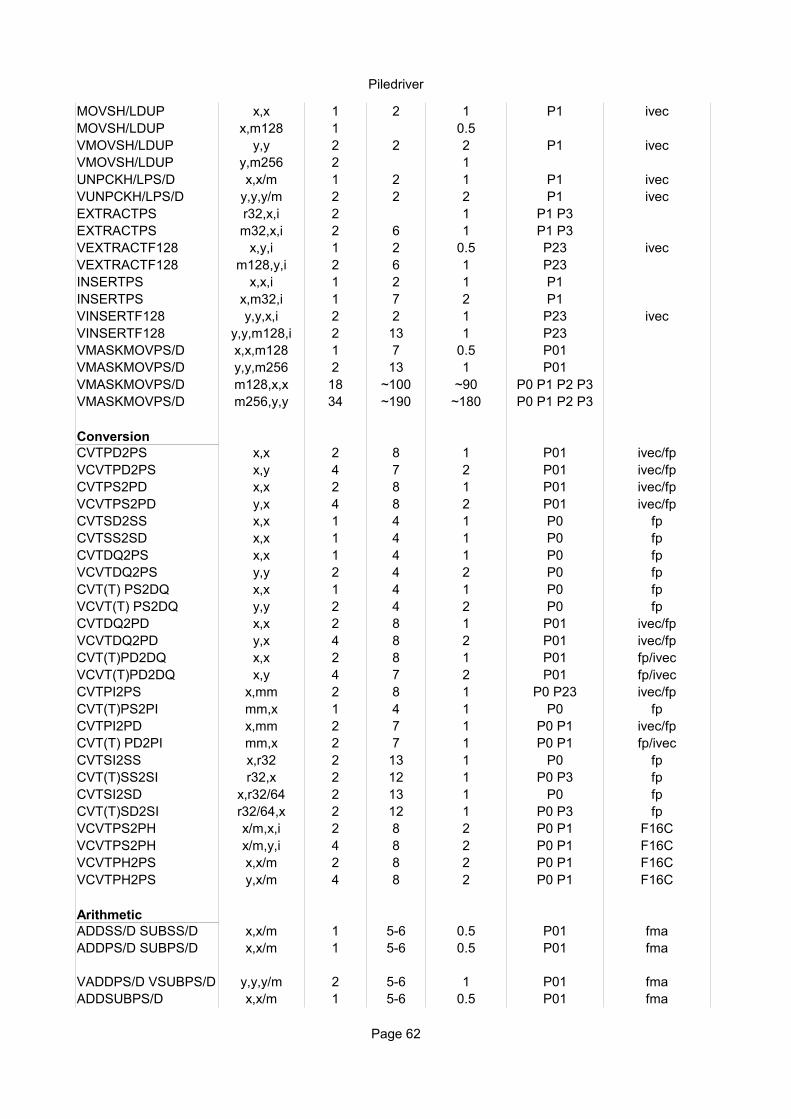
Piledriver
Page 62
MOVSH/LDUP x,x 1 2 1 P1 ivecMOVSH/LDUP x,m128 1 0.5VMOVSH/LDUP y,y 2 2 2 P1 ivecVMOVSH/LDUP y,m256 2 1UNPCKH/LPS/D x,x/m 1 2 1 P1 ivecVUNPCKH/LPS/D y,y,y/m 2 2 2 P1 ivecEXTRACTPS r32,x,i 2 1 P1 P3EXTRACTPS m32,x,i 2 6 1 P1 P3VEXTRACTF128 x,y,i 1 2 0.5 P23 ivecVEXTRACTF128 m128,y,i 2 6 1 P23INSERTPS x,x,i 1 2 1 P1INSERTPS x,m32,i 1 7 2 P1VINSERTF128 y,y,x,i 2 2 1 P23 ivecVINSERTF128 y,y,m128,i 2 13 1 P23VMASKMOVPS/D x,x,m128 1 7 0.5 P01VMASKMOVPS/D y,y,m256 2 13 1 P01VMASKMOVPS/D m128,x,x 18 ~100 ~90 P0 P1 P2 P3VMASKMOVPS/D m256,y,y 34 ~190 ~180 P0 P1 P2 P3
ConversionCVTPD2PS x,x 2 8 1 P01 ivec/fpVCVTPD2PS x,y 4 7 2 P01 ivec/fpCVTPS2PD x,x 2 8 1 P01 ivec/fpVCVTPS2PD y,x 4 8 2 P01 ivec/fpCVTSD2SS x,x 1 4 1 P0 fpCVTSS2SD x,x 1 4 1 P0 fpCVTDQ2PS x,x 1 4 1 P0 fpVCVTDQ2PS y,y 2 4 2 P0 fpCVT(T) PS2DQ x,x 1 4 1 P0 fpVCVT(T) PS2DQ y,y 2 4 2 P0 fpCVTDQ2PD x,x 2 8 1 P01 ivec/fpVCVTDQ2PD y,x 4 8 2 P01 ivec/fpCVT(T)PD2DQ x,x 2 8 1 P01 fp/ivecVCVT(T)PD2DQ x,y 4 7 2 P01 fp/ivecCVTPI2PS x,mm 2 8 1 P0 P23 ivec/fpCVT(T)PS2PI mm,x 1 4 1 P0 fpCVTPI2PD x,mm 2 7 1 P0 P1 ivec/fpCVT(T) PD2PI mm,x 2 7 1 P0 P1 fp/ivecCVTSI2SS x,r32 2 13 1 P0 fpCVT(T)SS2SI r32,x 2 12 1 P0 P3 fpCVTSI2SD x,r32/64 2 13 1 P0 fpCVT(T)SD2SI r32/64,x 2 12 1 P0 P3 fpVCVTPS2PH x/m,x,i 2 8 2 P0 P1 F16CVCVTPS2PH x/m,y,i 4 8 2 P0 P1 F16CVCVTPH2PS x,x/m 2 8 2 P0 P1 F16CVCVTPH2PS y,x/m 4 8 2 P0 P1 F16C
ArithmeticADDSS/D SUBSS/D x,x/m 1 5-6 0.5 P01 fmaADDPS/D SUBPS/D x,x/m 1 5-6 0.5 P01 fma
VADDPS/D VSUBPS/D y,y,y/m 2 5-6 1 P01 fmaADDSUBPS/D x,x/m 1 5-6 0.5 P01 fma

Piledriver
Page 63
VADDSUBPS/D y,y,y/m 2 5-6 1 P01 fma
HADDPS/D HSUBPS/D x,x 3 10 2 P01 P1 ivec/fma
HADDPS/D HSUBPS/D x,m 4 2 P01 P1 ivec/fma
y,y,y/m 8 10 4 P01 P1 ivec/fmaMULSS MULSD x,x/m 1 5-6 0.5 P01 fmaMULPS MULPD x,x/m 1 5-6 0.5 P01 fmaVMULPS VMULPD y,y,y/m 2 5-6 1 P01 fmaDIVSS DIVPS x,x/m 1 9-24 5-10 P01 fpVDIVPS y,y,y/m 2 9-24 9-20 P01 fpDIVSD DIVPD x,x/m 1 9-27 5-10 P01 fpVDIVPD y,y,y/m 2 9-27 9-18 P01 fpRCPSS/PS x,x/m 1 5 1 P01 fpVRCPPS y,y/m 2 5 2 P01 fp
x,x/m 1 2 0.5 P01 fpVCMPPS/D y,y,y/m 2 2 1 P01 fp
x,x/m 2 1 P01 P3 fp
x,x/m 1 2 0.5 P01 fp
VMAXPS/D VMINPS/D y,y,y/m 2 2 1 P01 fpROUNDSS/SD/PS/PD x,x/m,i 1 4 1 P0 fp
y,y/m,i 2 4 2 P0 fpDPPS x,x,i 16 25 6 P01 P23 SSE4.1DPPS x,m,i 18 7 P01 P23 SSE4.1VDPPS y,y,y,i 25 27 13 P01 P3 SSE4.1VDPPS y,m,i 29 13 P01 P3 SSE4.1DPPD x,x,i 15 15 5 P01 P23 SSE4.1DPPD x,m,i 17 6 P01 P23 SSE4.1VFMADD132SS/SD x,x,x/m 1 5-6 1 P01 FMA3VFMADD132PS/PD x,x,x/m 1 5-6 1 P01 FMA3VFMADD132PS/PD y,y,y/m 2 5-6 1 P01 FMA3All other FMA3 instructions: same as above FMA3VFMADDSS/SD x,x,x,x/m 1 5-6 0.5 P01 AMD FMA4VFMADDPS/PD x,x,x,x/m 1 5-6 0.5 P01 AMD FMA4VFMADDPS/PD y,y,y,y/m 2 5-6 1 P01 AMD FMA4All other FMA4 instructions: same as above AMD FMA4
MathSQRTSS/PS x,x/m 1 13-15 5-12 P01 fpVSQRTPS y,y/m 2 14-15 9-24 P01 fpSQRTSD/PD x,x/m 1 24-26 5-15 P01 fpVSQRTPD y,y/m 2 24-26 9-29 P01 fpRSQRTSS/PS x,x/m 1 5 1 P01 fpVRSQRTPS y,y/m 2 5 2 P01 fpVFRCZSS/SD/PS/PD x,x 2 10 2 P01 AMD XOPVFRCZSS/SD/PS/PD x,m 3 10 2 P01 AMD XOP
VHADDPS/DVHSUBPS/D
CMPSS/DCMPPS/D
COMISS/D UCOMISS/D
MAXSS/SD/PS/PD MINSS/SD/PS/PD
VROUNDSS/SD/PS/ PD

Piledriver
Page 64
Logic
x,x/m 1 2 0.5 P23 ivec
y,y,y/m 2 2 1 P23 ivec
OtherVZEROUPPER 9 4 P2 P3 32 bit modeVZEROUPPER 16 5 P2 P3 64 bit modeVZEROALL 17 6 P2 P3 32 bit modeVZEROALL 32 10 P2 P3 64 bit modeLDMXCSR m32 7 34 P0 P3STMXCSR m32 2 17 P0 P3FXSAVE m4096 67 136 136 P0 P1 P2 P3FXRSTOR m4096 116 176 176 P0 P1 P2 P3XSAVE m 122 196 196 P0 P1 P2 P3XRSTOR m 177 250 250 P0 P1 P2 P3
AND/ANDN/OR/XORPS/ PD
VAND/ANDN/OR/XORPS/PD

Steamroller
Page 65
AMD SteamrollerList of instruction timings and macro-operation breakdown
Explanation of column headings:Instruction:
Operands:
Ops:
Latency:
Execution pipe:
Domain:
Integer instructions
Instruction name. cc means any condition code. For example, Jcc can be JB, JNE, etc.
i = immediate constant, r = any register, r32 = 32-bit register, etc., mm = 64 bit mmx register, x = 128 bit xmm register, y = 256 bit ymm register, m = any memory operand including indirect operands, m64 means 64-bit memory operand, etc.
Number of macro-operations issued from instruction decoder to schedulers. In-structions with more than 2 macro-operations use microcode.
This is the delay that the instruction generates in a dependency chain. The num-bers are minimum values. Cache misses, misalignment, and exceptions may in-crease the clock counts considerably. The latency listed does not include the memory operand where the listing for register and memory operand are joined (r/m).
Reciprocal through-put:
This is also called issue latency. This value indicates the average number of clock cycles from the execution of an instruction begins to a subsequent independent in-struction of the same kind can begin to execute. A value of 1/3 indicates that the execution units can handle 3 instructions per clock cycle in one thread. However, the throughput may be limited by other bottlenecks in the pipeline.
Indicates which execution pipe or unit is used for the macro-operations:Integer pipes:EX0: integer ALU, divisionEX1: integer ALU, multiplication, jumpEX01: can use either EX0 or EX1AG01: address generation unit 0 or 1Floating point and vector pipes:P0: floating point add, mul, div. Integer add, mul, boolP1: floating point add, mul, div. Shuffle, shift, packP2: Integer add. Bool, storeP01: can use either P0 or P1P02: can use either P0 or P2Two macro-operations can execute simultaneously if they go to differentexecution pipes
Tells which execution unit domain is used:ivec: integer vector execution unit.fp: floating point execution unit.fma: floating point multiply/add subunit.inherit: the output operand inherits the domain of the input operand.ivec/fma means the input goes to the ivec domain and the output comes from the fma domain.There is an additional latency of 1 clock cycle if the output of an ivec instruction goes to the input of a fp or fma instruction, and when the output of a fp or fma in-struction goes to the input of an ivec or store instruction. There is no latency be-tween the fp and fma units. All other latencies after memory load and before memory store instructions are included in the latency counts.An fma instruction has a latency of 5 if the output goes to another fma instruction, 6 if the output goes to an fp instuction, and 6+1 if the output goes to an ivec or store instruction.

Steamroller
Page 66
Instruction Operands Ops Latency Notes
Move instructionsMOV r8,r8 1 1 0.5 EX01MOV r16,r16 1 1 0.5 EX01MOV r32,r32 1 1 0.25 EX01 or AG01MOV r64,r64 1 1 0.25 EX01 or AG01MOV r,i 1 1 0.5 EX01MOV r,m 1 3 0.5 AG01 all addr. modesMOV m,r 1 4 1 EX01 AG01 all addr. modesMOV m,i 1 1MOVNTI m,r 1 4 1MOVZX, MOVSX r,r 1 1 0.5 EX01MOVSX r,m 1 5 0.5 EX01MOVZX r,m 1 4 0.5 EX01MOVSXD r64,r32 1 1 0.5 EX01MOVSXD r64,m32 1 5 0.5 EX01CMOVcc r,r 1 1 0.5 EX01CMOVcc r,m 1 0.5 EX01XCHG r8,r8 2 1 1 EX01XCHG r16,r16 2 1 1 EX01XCHG r32,r32 2 1 0.5 EX01XCHG r64,r64 2 1 0.5 EX01
XCHG r,m 2 ~38 ~38 EX01XLAT 2 6 2PUSH r 1 1PUSH i 1 1PUSH m 2 1PUSHF(D/Q) 8 4PUSHA(D) 9 9POP r 1 1POP m 2 1POPF(D/Q) 34 19POPA(D) 14 8POP sp 1 2LEA r16,[m] 2 2-3 EX01 any addr. sizeLEA r32,[m] 1 2 EX01 16 bit addr. size
LEA r32/64,[m] 1 2 0.5 EX01LEA r32/64,[m] 1 1 0.5 EX01 all other casesLAHF 4 3 2SAHF 2 2 1SALC 1 1 1BSWAP r 1 1 0.5 EX01PREFETCHNTA m 1 0.5PREFETCHT0/1/2 m 1 0.5PREFETCH/W m 1 0.5 PREFETCHWSFENCE 7 ~80LFENCE 1 0,25MFENCE 7 ~80
Arithmetic instructions
Reciprocal throughput
Execution pipes
Timing depends on hw
scale factor > 1 or 3 operands

Steamroller
Page 67
ADD, SUB r,r 1 1 0.5 EX01ADD, SUB r,i 1 1 0.5 EX01ADD, SUB r,m 1 0.5 EX01ADD, SUB m,r 1 7 1 EX01ADD, SUB m,i 1 7 1 EX01ADC, SBB r,r 1 1 EX01ADC, SBB r,i 1 1 EX01ADC, SBB r,m 1 1 1 EX01ADC, SBB m,r 1 9 1 EX01ADC, SBB m,i 1 9 1 EX01CMP r,r 1 1 0.5 EX01CMP r,i 1 1 0.5 EX01CMP r,m 1 0.5 EX01CMP m,i 1 0.5 EX01INC, DEC, NEG r 1 1 0.5 EX01INC, DEC, NEG m 1 7 1 EX01AAA, AAS 10 6DAA 16 8DAS 20 10AAD 4 6AAM 10 15 15MUL, IMUL r8/m8 1 4 2 EX1MUL, IMUL r16/m16 2 4 2 EX1MUL, IMUL r32/m32 1 4 2 EX1MUL, IMUL r64/m64 1 6 4 EX1IMUL r16,r16/m16 1 4 2 EX1IMUL r32,r32/m32 1 4 2 EX1IMUL r64,r64/m64 1 6 4 EX1IMUL r16,(r16),i 2 5 2 EX1IMUL r32,(r32),i 1 4 2 EX1IMUL r64,(r64),i 1 6 4 EX1IMUL r16,m16,i 2 2 EX1IMUL r32,m32,i 2 2 EX1IMUL r64,m64,i 2 4 EX1DIV r8/m8 9 17-22 13-17 EX0DIV r16/m16 7 15-25 15-25 EX0DIV r32/m32 2 13-39 13-39 EX0DIV r64/m64 2 13-70 13-70 EX0IDIV r8/m8 9 17-22 13-17 EX0IDIV r16/m16 7 14-25 14-24 EX0IDIV r32/m32 2 13-39 13-39 EX0IDIV r64/m64 2 13-70 13-70 EX0CBW, CWDE, CDQE 1 1 EX01CDQ, CQO 1 1 0.5 EX01CWD 2 1 1 EX01
Logic instructionsAND, OR, XOR r,r 1 1 0.5 EX01AND, OR, XOR r,i 1 1 0.5 EX01AND, OR, XOR r,m 1 0.5 EX01AND, OR, XOR m,r 1 7 1 EX01AND, OR, XOR m,i 1 7 1 EX01TEST r,r 1 1 0.5 EX01
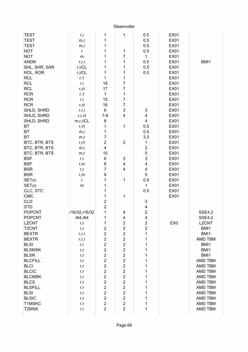
Steamroller
Page 68
TEST r,i 1 1 0.5 EX01TEST m,r 1 0.5 EX01TEST m,i 1 0.5 EX01NOT r 1 1 0.5 EX01NOT m 1 7 1 EX01ANDN r,r,r 1 1 0.5 EX01 BMI1SHL, SHR, SAR r,i/CL 1 1 0.5 EX01ROL, ROR r,i/CL 1 1 0.5 EX01RCL r,1 1 1 EX01RCL r,i 16 7 EX01RCL r,cl 17 7 EX01RCR r,1 1 1 EX01RCR r,i 15 7 EX01RCR r,cl 16 7 EX01SHLD, SHRD r,r,i 6 3 3 EX01SHLD, SHRD r,r,cl 7-8 4 4 EX01SHLD, SHRD m,r,i/CL 8 4 EX01BT r,r/i 1 1 0.5 EX01BT m,i 1 0.5 EX01BT m,r 7 3,5 EX01BTC, BTR, BTS r,r/i 2 2 1 EX01BTC, BTR, BTS m,i 4 2 EX01BTC, BTR, BTS m,r 10 5 EX01BSF r,r 6 3 3 EX01BSF r,m 8 4 4 EX01BSR r,r 7 4 4 EX01BSR r,m 9 5 EX01SETcc r 1 1 0.5 EX01SETcc m 1 1 EX01CLC, STC 1 0.5 EX01CMC 1 1 EX01CLD 2 3STD 2 4POPCNT r16/32,r16/32 1 4 2 SSE4.2POPCNT r64,r64 1 4 4 SSE4.2LZCNT r,r 1 2 2 EX0 LZCNTTZCNT r,r 2 2 2 BMI1BEXTR r,r,r 2 2 1 BMI1BEXTR r,r,i 2 2 1 AMD TBMBLSI r,r 2 2 1 BMI1BLSMSK r,r 2 2 1 BMI1BLSR r,r 2 2 1 BMI1BLCFILL r,r 2 2 1 AMD TBMBLCI r,r 2 2 1 AMD TBMBLCIC r,r 2 2 1 AMD TBMBLCMSK r,r 2 2 1 AMD TBMBLCS r,r 2 2 1 AMD TBMBLSFILL r,r 2 2 1 AMD TBMBLSI r,r 2 2 1 AMD TBMBLSIC r,r 2 2 1 AMD TBMT1MSKC r,r 2 2 1 AMD TBMTZMSK r,r 2 2 1 AMD TBM

Steamroller
Page 69
Control transfer instructionsJMP short/near 1 2 EX1JMP r 1 2 EX1JMP m 1 2 EX1Jcc short/near 1 1-2 EX1 2 if jumpingfused CMP+Jcc short/near 1 1-2 EX1 2 if jumpingJ(E/R)CXZ short 1 1-2 EX1 2 if jumpingLOOP short 1 1-2 EX1 2 if jumpingLOOPE LOOPNE short 1 1-2 EX1 2 if jumpingCALL near 2 2 EX1CALL r 2 2 EX1CALL m 3 2 EX1RET 1 2 EX1RET i 4 2 EX1BOUND m 11 5 for no jumpINTO 4 2 for no jump
String instructionsLODS 3 3REP LODS m8/m16 6n 3nREP LODS m32/m64 6n 2.5nSTOS 3 3REP STOS 1n ~1n small nREP STOS 3 per 16B 2 per 16B best caseMOVS 5 3REP MOVS ~1n ~1n small nREP MOVS 4-5 pr 16B ~2 per 16B best caseSCAS 3 3REP SCAS 7n 3-4nCMPS 6 3REP CMPS 9n 4n
SynchronizationLOCK ADD m,r 1 ~39XADD m,r 4 9-12LOCK XADD m,r 4 ~39CMPXCHG m,r8 5 15CMPXCHG m,r16 6 15CMPXCHG m,r32/64 6 13LOCK CMPXCHG m8,r8 5 ~40LOCK CMPXCHG m16,r16 6 ~40LOCK CMPXCHG m,r32/64 6 ~40CMPXCHG8B m64 18 ~14LOCK CMPXCHG8B m64 18 ~42CMPXCHG16B m128 24 ~47LOCK CMPXCHG16B m128 24 ~80
OtherNOP (90) 1 0.25 noneLong NOP (0F 1F) 1 0.25 nonePAUSE 8 4ENTER a,0 13 21ENTER a,b 11+5b 20-30
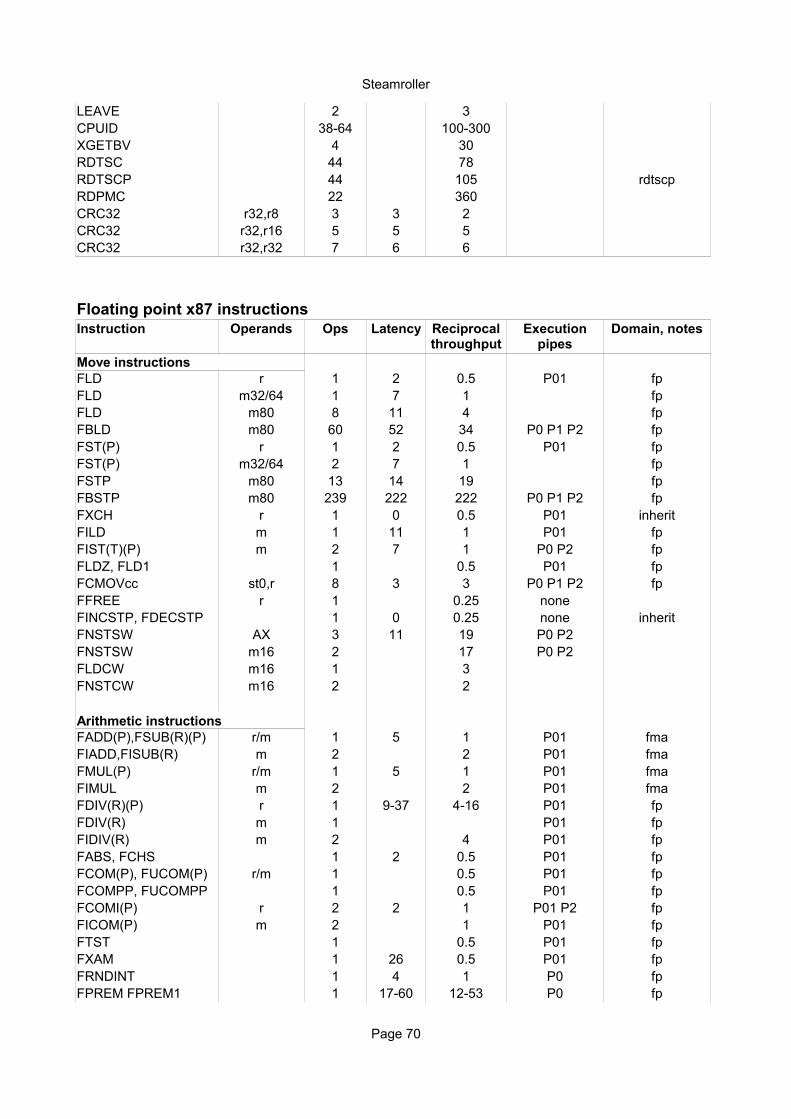
Steamroller
Page 70
LEAVE 2 3CPUID 38-64 100-300XGETBV 4 30RDTSC 44 78RDTSCP 44 105 rdtscpRDPMC 22 360CRC32 r32,r8 3 3 2CRC32 r32,r16 5 5 5CRC32 r32,r32 7 6 6
Floating point x87 instructionsInstruction Operands Ops Latency Domain, notes
Move instructionsFLD r 1 2 0.5 P01 fpFLD m32/64 1 7 1 fpFLD m80 8 11 4 fpFBLD m80 60 52 34 P0 P1 P2 fpFST(P) r 1 2 0.5 P01 fpFST(P) m32/64 2 7 1 fpFSTP m80 13 14 19 fpFBSTP m80 239 222 222 P0 P1 P2 fpFXCH r 1 0 0.5 P01 inheritFILD m 1 11 1 P01 fpFIST(T)(P) m 2 7 1 P0 P2 fpFLDZ, FLD1 1 0.5 P01 fpFCMOVcc st0,r 8 3 3 P0 P1 P2 fpFFREE r 1 0.25 noneFINCSTP, FDECSTP 1 0 0.25 none inheritFNSTSW AX 3 11 19 P0 P2FNSTSW m16 2 17 P0 P2FLDCW m16 1 3FNSTCW m16 2 2
Arithmetic instructionsFADD(P),FSUB(R)(P) r/m 1 5 1 P01 fmaFIADD,FISUB(R) m 2 2 P01 fmaFMUL(P) r/m 1 5 1 P01 fmaFIMUL m 2 2 P01 fmaFDIV(R)(P) r 1 9-37 4-16 P01 fpFDIV(R) m 1 P01 fpFIDIV(R) m 2 4 P01 fpFABS, FCHS 1 2 0.5 P01 fpFCOM(P), FUCOM(P) r/m 1 0.5 P01 fpFCOMPP, FUCOMPP 1 0.5 P01 fpFCOMI(P) r 2 2 1 P01 P2 fpFICOM(P) m 2 1 P01 fpFTST 1 0.5 P01 fpFXAM 1 26 0.5 P01 fpFRNDINT 1 4 1 P0 fpFPREM FPREM1 1 17-60 12-53 P0 fp
Reciprocal throughput
Execution pipes

Steamroller
Page 71
MathFSQRT 1 10-50 5-20 P01FLDPI, etc. 1 0.5 P01FSIN 10-164 60-210 60-165 P0 P1 P2FCOS 18-166 76-158 P0 P1 P2FSINCOS 12-168 90-165 P0 P1 P2FPTAN 11-192 90-245 90-210 P0 P1 P2FPATAN 10-365 60-440 60-365 P0 P1 P2FSCALE 10 49 5 P0 P1 P2FXTRACT 12 8 5 P0 P1 P2F2XM1 10-18 60-74 P0 P1 P2FYL2X 9-183 60-280 P0 P1 P2FYL2XP1 206 ~390 P0 P1 P2
OtherFNOP 1 0.25 none(F)WAIT 1 0.25 noneFNCLEX 18 63 P0FNINIT 31 131 P0FNSAVE m864 98 256 256 P0 P1 P2FRSTOR m864 73 166 166 P0 P2
Integer vector instructionsInstruction Operands Ops Latency Notes
Move instructionsMOVD r32/64, mm/x 1 4 1 P2MOVD mm/x, r32/64 2 5 1MOVD mm/x,m32 1 2 0.5MOVD m32,mm/x 1 3 1MOVQ mm/x,mm/x 1 2 0.5 P02MOVQ mm/x,m64 1 2 0.5MOVQ m64,mm/x 1 3 1MOVDQA xmm,xmm 1 0 0.25 none inherit domainMOVDQA xmm,m 1 2 0.5MOVDQA m,xmm 1 3 1 P2VMOVDQA ymm,ymm 2 2 0.5 P02VMOVDQA ymm,m256 2 3 1VMOVDQA m256,ymm 2 4 1 P2MOVDQU xmm,xmm 1 0 0.25 none inherit domainMOVDQU xmm,m 1 2 0.5MOVDQU m,xmm 1 3 1 P2LDDQU xmm,m 1 2 0.5VMOVDQU ymm,m256 2 3 1VMOVDQU m256,ymm 2 4 1MOVDQ2Q mm,xmm 1 1 0.5 P02MOVQ2DQ xmm,mm 1 1 0.5 P02MOVNTQ m,mm 1 3 1 P2MOVNTDQ m,xmm 1 3 1 P2MOVNTDQA xmm,m 1 2 0.5
Reciprocal throughput
Execution pipes

Steamroller
Page 72
PACKSSWB/DW (x)mm,r/m 1 2 1 P1PACKUSWB (x)mm,r/m 1 2 1 P1
(x)mm,r/m 1 2 1 P1PUNPCKHQDQ xmm,r/m 1 2 1 P1PUNPCKLQDQ xmm,r/m 1 2 1 P1PSHUFB (x)mm,r/m 1 3 1 P1PSHUFD xmm,xmm,i 1 2 1 P1PSHUFW mm,mm,i 1 2 1 P1PSHUFL/HW xmm,xmm,i 1 2 1 P1PALIGNR (x)mm,r/m,i 1 2 1 P1PBLENDW xmm,r/m 1 2 0.5 P02 SSE4.1MASKMOVQ mm,mm 31 32 16 P2MASKMOVDQU xmm,xmm 65 45 31 P0 P1 P2PMOVMSKB r32,mm/x 2 5 1 P1 P2PEXTRB/W/D/Q r,x/mm,i 2 5 1 P1 P2 SSE4.1PINSRB/W/D/Q x/mm,r,i 2 6 1 P1EXTRQ x,i,i 1 3 1 P1 AMD SSE4AEXTRQ x,x 1 1 1 P1 AMD SSE4AINSERTQ x,x,i,i 1 1 1 P1 AMD SSE4AINSERTQ x,x 1 1 1 P1 AMD SSE4A
x,x 1 2 1 P1 SSE4.1
x,x 1 2 1 P1 SSE4.1VPCMOV x,x,x,x/m 1 2 1 P1 AMD XOPVPCMOV y,y,y,y/m 2 2 2 P1 AMD XOPVPPERM x,x,x,x/m 1 2 1 P1 AMD XOP
Arithmetic instructions
(x)mm,r/m 1 2 0.5 P02
(x)mm,r/m 1 2 0.5 P02PHADD/SUB(S)W/D x,x 3 5 2 P02 2P1 SSSE3PCMPEQ/GT B/W/D (x)mm,r/m 1 2 0.5 P02PCMPEQQ (x)mm,r/m 1 2 0.5 P02 SSE4.1PCMPGTQ (x)mm,r/m 1 2 0.5 P02 SSE4.2
(x)mm,r/m 1 4 1 P0PMULLD x,r/m 1 5 2 P0 SSE4.1PMULDQ x,r/m 1 4 1 P0 SSE4.1PMULHRSW (x)mm,r/m 1 4 1 P0 SSSE3PMADDWD (x)mm,r/m 1 4 1 P0PMADDUBSW (x)mm,r/m 1 4 1 P0PAVGB/W (x)mm,r/m 1 2 0.5 P02
(x)mm,r/m 1 2 0.5 P02PHMINPOSUW x,r/m 2 4 1 P1 P02 SSE4.1PABSB/W/D (x)mm,r/m 1 2 0.5 P02 SSSE3PSIGNB/W/D (x)mm,r/m 1 2 0.5 P02 SSSE3PSADBW (x)mm,r/m 2 4 1 P02
PUNPCKH/LBW/WD/DQ
PMOVSXBW/BD/BQ/WD/WQ/DQ
PMOVZXBW/BD/BQ/WD/WQ/DQ
PADDB/W/D/Q/SB/SW/USB/USW
PSUBB/W/D/Q/SB/SW/USB/USW
PMULLW PMULHW PMULHUW PMULUDQ
PMIN/MAX SB/SW/ SD UB/UW/UD

Steamroller
Page 73
MPSADBW x,x,i 8 8 4 P1 P02 SSE4.1
VPCOMB/W/D/Q x,x,x/m,i 1 2 0.5 P02
VPCOMUB/W/D/Q x,x,x/m,i 1 2 0.5 P02
x,x/m 1 2 0.5 P02 AMD XOP
x,x/m 1 2 0.5 P02 AMD XOPVPHSUBBW/WD/DQ x,x/m 1 2 0.5 P02 AMD XOPVPMACSWW/WD x,x,x/m,x 1 4 1 P0 AMD XOPVPMACSDD x,x,x/m,x 1 5 2 P0 AMD XOPVPMACSDQH/L x,x,x/m,x 1 4 1 P0 AMD XOPVPMACSSWW/WD x,x,x/m,x 1 4 1 P0 AMD XOPVPMACSSDD x,x,x/m,x 1 5 2 P0 AMD XOPVPMACSSDQH/L x,x,x/m,x 1 4 1 P0 AMD XOPVPMADCSWD x,x,x/m,x 1 4 1 P0 AMD XOPVPMADCSSWD x,x,x/m,x 1 4 1 P0 AMD XOP
Logic
(x)mm,r/m 1 2 0.5 P02
(x)mm,r/m 1 3 1 P1
(x)mm,i 1 2 1 P1PSLLDQ, PSRLDQ x,i 1 2 1 P1PTEST x,r/m 2 14 1 P1 P2 SSE4.1VPROTB/W/D/Q x,x,x/m 1 3 1 P1 AMD XOPVPROTB/W/D/Q x,x,i 1 2 1 P1 AMD XOPVPSHAB/W/D/Q x,x,x/m 1 3 1 P1 AMD XOPVPSHLB/W/D/Q x,x,x/m 1 3 1 P1 AMD XOP
String instructionsPCMPESTRI x,x,i 30 11 11 P0 P1 P2 SSE4.2PCMPESTRM x,x,i 30 10 10 P0 P1 P2 SSE4.2PCMPISTRI x,x,i 9 5 5 P0 P1 P2 SSE4.2PCMPISTRM x,x,i 8 6 6 P0 P1 P2 SSE4.2
EncryptionPCLMULQDQ x,x/m,i 7 11 7 P1 pclmulVPCLMULQDQ x,x,x,i 7 11 7 P1 pclmulPCLMULQDQ x,x,m,i 8 7 P1 pclmulAESDEC x,x 2 5 1 P01 aesAESDECLAST x,x 2 5 1 P01 aesAESENC x,x 2 5 1 P01 aesAESENCLAST x,x 2 5 1 P01 aesAESIMC x,x 1 5 1 P0 aesAESKEYGENASSIST x,x,i 1 5 1 P0 aes
OtherEMMS 1 0.25
AMD XOP latency 0 if i=6,7
AMD XOP latency 0 if i=6,7
VPHADDBW/BD/BQ/ WD/WQ/DQ
VPHADDUBW/BD/BQ/WD/WQ/DQ
PAND PANDN POR PXOR
PSLL/RL W/D/Q PSRAW/D
PSLL/RL W/D/Q PSRAW/D

Steamroller
Page 74
Floating point XMM and YMM instructionsInstruction Operands Ops Latency Domain, notes
Move instructions
x,x 1 0 0.25 none inherit domainVMOVAPS/D y,y 2 2 0.5 P02 ivec
x,m128 1 2 0.5
y,m256 2 2 1
m128,x 1 3 1 P2VMOVAPS/D m256,y 2 3 2 P2VMOVUPS/D m256,y 2 3 2 P2MOVSS/D x,x 1 2 0.5 P01 fpMOVSS/D x,m32/64 1 2 0.5MOVSS/D m32/64,x 1 3 1 P2MOVHPS/D x,m64 1 3 1 P1MOVLPS/D x,m64 1 3 0.5 P01MOVHPS/D m64,x 2 4 1 P1 P2MOVLPS/D m64,x 1 3 1 P2MOVLHPS MOVHLPS x,x 1 2 1 P1 ivecMOVMSKPS/D r32,x 2 5 1 P1 P2VMOVMSKPS/D r32,y 2 15 1 P1 P2MOVNTPS/D m128,x 1 3 1 P2VMOVNTPS/D m256,y 2 3 2-3 P2MOVNTSS/SD m,x 1 3 P2 AMD SSE4ASHUFPS/D x,x/m,i 1 2 1 P2 ivecVSHUFPS/D y,y,y/m,i 2 2 2 P2 ivecVPERMILPS/PD x,x,x/m 1 3 1 P1 ivecVPERMILPS/PD y,y,y/m 2 3 2 P1 ivecVPERMILPS/PD x,x/m,i 1 2 1 P1 ivecVPERMILPS/PD y,y/m,i 2 2 2 P1 ivecVPERM2F128 y,y,y,i 8 4 3.5 P0 P2 ivecVPERM2F128 y,y,m,i 12 4 P0 P2 ivecBLENDPS/PD x,x/m,i 1 2 0.5 P01 fpVBLENDPS/PD y,y,y/m,i 2 2 1 P01 fpBLENDVPS/PD x,x/m,xmm0 1 2 0.5 P01VBLENDVPS/PD y,y,y/m,y 2 2 1 P01MOVDDUP x,x 1 2 1 P1 ivecMOVDDUP x,m64 1 0.5VMOVDDUP y,y 2 2 2 P1 ivecVMOVDDUP y,m256 2 1VBROADCASTSS x,m32 1 8 0.5VBROADCASTSS y,m32 2 8 0.5 P02VBROADCASTSD y,m64 2 8 0.5 P02VBROADCASTF128 y,m128 2 8 0.5 P02MOVSH/LDUP x,x 1 2 1 P1 ivecMOVSH/LDUP x,m128 1 0.5
Reciprocal throughput
Execution pipes
MOVAPS/D MOVUPS/D
MOVAPS/D MOVUPS/DVMOVAPS/D VMOVUPS/D
MOVAPS/D MOVUPS/D

Steamroller
Page 75
VMOVSH/LDUP y,y 2 2 2 P1 ivecVMOVSH/LDUP y,m256 2 1UNPCKH/LPS/D x,x/m 1 2 1 P1 ivecVUNPCKH/LPS/D y,y,y/m 2 2 2 P1 ivecEXTRACTPS r32,x,i 2 1 P1 P2EXTRACTPS m32,x,i 2 10 1 P1 P2VEXTRACTF128 x,y,i 1 2 0.5 P02 ivecVEXTRACTF128 m128,y,i 2 10 1 P0 P2INSERTPS x,x,i 1 2 1 P1INSERTPS x,m32,i 1 9 2 P1VINSERTF128 y,y,x,i 2 2 1 P02 ivecVINSERTF128 y,y,m128,i 2 10 1 P02VMASKMOVPS/D x,x,m128 1 9 0.5 P01VMASKMOVPS/D y,y,m256 2 9 1 P01VMASKMOVPS/D m128,x,x 20 ~35 8 P0 P1 P2VMASKMOVPS/D m256,y,y 41 ~35 16 P0 P1 P2
ConversionCVTPD2PS x,x 2 6 1 P01 ivec/fpVCVTPD2PS x,y 4 6 2 P01 ivec/fpCVTPS2PD x,x 2 6 1 P01 ivec/fpVCVTPS2PD y,x 4 6 2 P01 ivec/fpCVTSD2SS x,x 1 4 1 P0 fpCVTSS2SD x,x 1 4 1 P0 fpCVTDQ2PS x,x 1 4 1 P0 fpVCVTDQ2PS y,y 2 4 2 P0 fpCVT(T) PS2DQ x,x 1 4 1 P0 fpVCVT(T) PS2DQ y,y 2 4 2 P0 fpCVTDQ2PD x,x 2 7 1 P01 ivec/fpVCVTDQ2PD y,x 4 7 2 P01 ivec/fpCVT(T)PD2DQ x,x 2 7 1 P01 fp/ivecVCVT(T)PD2DQ x,y 4 7 2 P01 fp/ivecCVTPI2PS x,mm 2 6 1 P0 P2 ivec/fpCVT(T)PS2PI mm,x 1 5 1 P0 fpCVTPI2PD x,mm 2 7 1 P0 P1 ivec/fpCVT(T) PD2PI mm,x 2 7 1 P0 P1 fp/ivecCVTSI2SS x,r32 2 13 1 P0 fpCVT(T)SS2SI r32,x 2 12 1 P0 P2 fpCVTSI2SD x,r32/64 2 12 1 P0 fpCVT(T)SD2SI r32/64,x 2 12 1 P0 P2 fpVCVTPS2PH x/m,x,i 2 7 2 P0 P1 F16CVCVTPS2PH x/m,y,i 4 7 2 P0 P1 F16CVCVTPH2PS x,x/m 2 7 2 P0 P1 F16CVCVTPH2PS y,x/m 4 7 2 P0 P1 F16C
ArithmeticADDSS/D SUBSS/D x,x/m 1 5-6 1 P01 fmaADDPS/D SUBPS/D x,x/m 1 5-6 1 P01 fma
VADDPS/D VSUBPS/D y,y,y/m 2 5-6 2 P01 fmaADDSUBPS/D x,x/m 1 5-6 1 P01 fmaVADDSUBPS/D y,y,y/m 2 5-6 1 P01 fma

Steamroller
Page 76
HADDPS/D HSUBPS/D x,x 4 10 2 P0 P1 ivec/fma
y,y,y/m 8 10 4 P01 P1 ivec/fmaMULSS MULSD x,x/m 1 5-6 0.5 P01 fmaMULPS MULPD x,x/m 1 5-6 0.5 P01 fmaVMULPS VMULPD y,y,y/m 2 5-6 1 P01 fmaDIVSS DIVPS x,x/m 1 9-17 4-6 P01 fpVDIVPS y,y,y/m 2 9-17 9-12 P01 fpDIVSD DIVPD x,x/m 1 9-32 4-13 P01 fpVDIVPD y,y,y/m 2 9-32 9-27 P01 fpRCPSS/PS x,x/m 1 5 1 P01 fpVRCPPS y,y/m 2 5 2 P01 fp
x,x/m 1 2 0.5 P01 fpVCMPPS/D y,y,y/m 2 2 1 P01 fp
x,x/m 2 1 P01 P2 fp
x,x/m 1 2 0.5 P01 fp
VMAXPS/D VMINPS/D y,y,y/m 2 2 1 P01 fpROUNDSS/SD/PS/PD x,x/m,i 1 4 1 P0 fp
y,y/m,i 2 4 2 P0 fpDPPS x,x,i 9 25 4 P0 P1 SSE4.1DPPS x,m,i 10 5 P0 P1 SSE4.1VDPPS y,y,y,i 13 25 8 P0 P1 SSE4.1VDPPS y,m,i 15 8 P0 P1 SSE4.1DPPD x,x,i 7 14 3 P0 P1 SSE4.1DPPD x,m,i 8 4 P0 P1 SSE4.1VFMADD132SS/SD x,x,x/m 1 5-6 0.5 P01 FMA3VFMADD132PS/PD x,x,x/m 1 5-6 0.5 P01 FMA3VFMADD132PS/PD y,y,y/m 2 5-6 1 P01 FMA3All other FMA3 instructions: same as above FMA3VFMADDSS/SD x,x,x,x/m 1 5-6 0.5 P01 AMD FMA4VFMADDPS/PD x,x,x,x/m 1 5-6 0.5 P01 AMD FMA4VFMADDPS/PD y,y,y,y/m 2 5-6 1 P01 AMD FMA4All other FMA4 instructions: same as above AMD FMA4
MathSQRTSS/PS x,x/m 1 12-13 4-9 P01 fpVSQRTPS y,y/m 2 12-13 9-18 P01 fpSQRTSD/PD x,x/m 1 26-29 4-18 P01 fpVSQRTPD y,y/m 2 27-28 9-37 P01 fpRSQRTSS/PS x,x/m 1 5 1 P01 fpVRSQRTPS y,y/m 2 5 2 P01 fpVFRCZSS/SD/PS/PD x,x 2 10 2 P01 AMD XOPVFRCZSS/SD/PS/PD x,m 4 2 P01 AMD XOP
Logic
x,x/m 1 2 0.5 P02 ivec
VHADDPS/DVHSUBPS/D
CMPSS/DCMPPS/D
COMISS/D UCOMISS/D
MAXSS/SD/PS/PD MINSS/SD/PS/PD
VROUNDSS/SD/PS/ PD
AND/ANDN/OR/XORPS/ PD

Steamroller
Page 77
y,y,y/m 2 2 1 P02 ivec
OtherVZEROUPPER 9 4 32 bit modeVZEROUPPER 16 5 64 bit modeVZEROALL 17 6 P02 32 bit modeVZEROALL 32 10 P02 64 bit modeLDMXCSR m32 9 36 P0 P2STMXCSR m32 2 17 P0 P2FXSAVE m4096 59-67 78 P0 P1 P2FXRSTOR m4096 104-112 160 P0 P1 P2XSAVE m 121-137 147-166 P0 P1 P2XRSTOR m 191-209 291-297 P0 P1 P2
VAND/ANDN/OR/XORPS/PD

Ryzen
Page 78
AMD RyzenList of instruction timings and macro-operation breakdown
Explanation of column headings:Instruction:
Operands:
Ops: Number of macro-operations issued from instruction decoder to schedulers.Latency:
Execution pipe:
Domain:
Integer instructionsInstruction Operands Ops Latency Notes
Move instructionsMOV r8,r8 1 1 0.25MOV r16,r16 1 1 0.25MOV r32,r32 1 0 0.3 renamingMOV r64,r64 1 0 0.2 renamingMOV r8,i 1 0.25MOV r16,i 1 0.25MOV r32,i 1 0.25
Instruction name. cc means any condition code. For example, Jcc can be JB, JNE, etc.
i = immediate constant, r = any register, r32 = 32-bit register, etc., mm = 64 bit mmx register, x = 128 bit xmm register, y = 256 bit ymm register, m = any memory operand including indirect operands, m64 means 64-bit memory operand, etc.
This is the delay that the instruction generates in a dependency chain. The num-bers are minimum values. Cache misses, misalignment, and exceptions may in-crease the clock counts considerably. The latency listed does not include the memory operand where the listing for register and memory operand are joined (r/m).
Reciprocal through-put:
This is also called issue latency. This value indicates the average number of clock cycles from the execution of an instruction begins to a subsequent independent in-struction of the same kind can begin to execute. A value of 1/3 indicates that the execution units can handle 3 instructions per clock cycle in one thread. However, the throughput may be limited by other bottlenecks in the pipeline.
Indicates which execution pipe or unit is used for the macro-operations:P0: Floating point and vector pipe 0P1: Floating point and vector pipe 1P2: Floating point and vector pipe 2P3: Floating point and vector pipe 3P0 P1: Uses both P0 and P1P01: Uses either P0 and P1Where no unit is specified, it uses one or more integer pipe or address generation units.Two micro-operations can execute simultaneously if they go to differentexecution pipes
Tells which execution unit domain is used:ivec: integer vector execution unit.fp: floating point execution unit.inherit: the output operand inherits the domain of the input operand.There is an additional latency of 1 clock cycle if the output of an ivec instruction goes to the input of a fp instruction, and when the output of a fp instruction goes to the input of an ivec instruction. All other latencies after memory load and before memory store instructions are included in the latency counts.
Reciprocal throughput
Execution pipes

Ryzen
Page 79
MOV r64,i 1 0.25MOV r,m 1 3 0.5MOV m,r 1 4 1MOV m,i 1 1MOVNTI m,r 1 high 1MOVZX, MOVSX r,r 1 1 0.5MOVZX, MOVSX r,m 1 3 0.5MOVSXD r64,r32 1 1 0.5MOVSXD r64,m32 1 3 0.5CMOVcc r,r 1 1 0.25CMOVcc r,m 1 0.5XCHG r8,r8 2 1 1XCHG r16,r16 2 1 1XCHG r32,r32 2 0 0.33 renamingXCHG r64,r64 2 0 0.33 renamingXCHG r,m 2 ~30 ~30 depends on hw
XLAT 2 5 2PUSH r 1 1PUSH i 1 1PUSH m 2 1PUSHF(D/Q) 9 4PUSH sp 2 1PUSHA(D) 9 8POP r 1 0.5POP m 2 1POPF(D/Q) 35 13POPA(D) 9 4POP sp 1 2 2LEA r16,[m] 2 2-3 1
LEA r32/64,[m] 1 2 0.5LEA r32,[m] 1 2 0.5 64 bit modeLEA r32/64,[m] 1 0.5 rip relativeLEA r32/64,[m] 1 1 0.25 all other casesLAHF 4 3 2SAHF 2 2 0.5SALC 1 1 1BSWAP r 1 1 0.25MOVBE r,[m] 1 0.5 MOVBEMOVBE [m],r 1 1 MOVBEPREFETCHNTA m 1 0.5PREFETCHT0/1/2 m 1 0.5PREFETCH/W m 1 0.5 PREFETCHWSFENCE 4 ~20LFENCE 1 0,25MFENCE 7 ~70
Arithmetic instructionsADD, SUB r,r 1 1 0.25ADD, SUB r,i 1 1 0.25ADD, SUB r,m 1 0.5ADD, SUB m,r 1 6 1ADD, SUB m,i 1 6 1
scale factor > 1 or 3 operands
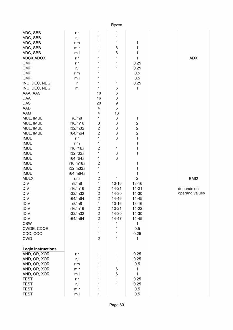
Ryzen
Page 80
ADC, SBB r,r 1 1ADC, SBB r,i 1 1ADC, SBB r,m 1 1 1ADC, SBB m,r 1 6 1ADC, SBB m,i 1 6 1ADCX ADOX r,r 1 1 1 ADXCMP r,r 1 1 0.25CMP r,i 1 1 0.25CMP r,m 1 0.5CMP m,i 1 0.5INC, DEC, NEG r 1 1 0.25INC, DEC, NEG m 1 6 1AAA, AAS 10 6DAA 16 8DAS 20 9AAD 4 5AAM 4 13MUL, IMUL r8/m8 1 3 1MUL, IMUL r16/m16 3 3 2MUL, IMUL r32/m32 2 3 2MUL, IMUL r64/m64 2 3 2IMUL r,r 1 3 1IMUL r,m 1 1IMUL r16,r16,i 2 4 1IMUL r32,r32,i 1 3 1IMUL r64,r64,i 1 3IMUL r16,m16,i 2 1IMUL r32,m32,i 1 1IMUL r64,m64,i 1 1MULX r,r,r 2 4 2 BMI2DIV r8/m8 1 13-16 13-16DIV r16/m16 2 14-21 14-21DIV r32/m32 2 14-30 14-30DIV r64/m64 2 14-46 14-45IDIV r8/m8 1 13-16 13-16IDIV r16/m16 2 13-21 14-22IDIV r32/m32 2 14-30 14-30IDIV r64/m64 2 14-47 14-45CBW 1 1 1CWDE, CDQE 1 1 0.5CDQ, CQO 1 1 0.25CWD 2 1 1
Logic instructionsAND, OR, XOR r,r 1 1 0.25AND, OR, XOR r,i 1 1 0.25AND, OR, XOR r,m 1 0.5AND, OR, XOR m,r 1 6 1AND, OR, XOR m,i 1 6 1TEST r,r 1 1 0.25TEST r,i 1 1 0.25TEST m,r 1 0.5TEST m,i 1 0.5
depends on operand values

Ryzen
Page 81
NOT r 1 1 0.25NOT m 1 6 1ANDN r,r,r 1 1 0.25 BMI1SHL, SHR, SAR r,i/CL 1 1 0.25ROL, ROR r,i/CL 1 1 0.25RCL r,1 1 1 1RCL r,i 9 4 4RCL r,cl 9 4 4RCR r,1 1 1 1RCR r,i 7 3 3RCR r,cl 7 3 3SHLD, SHRD r,r,i 6 3 3SHLD, SHRD r,r,cl 7 3 3SHLD, SHRD m,r,i/CL 8 3SARX r,r,r 1 1 0.25 BMI2SHLX r,r,r 1 1 0.25 BMI2SHRX r,r,r 1 1 0.25 BMI2RORX r,r,i 1 1 0.25 BMI2BT r,r/i 1 1 0.25BT m,i 1 0.5BT m,r 5 3BTC, BTR, BTS r,r/i 2 2 0.5BTC, BTR, BTS m,i 4 2BTC, BTR, BTS m,r 8 3BSF r,r 6 3 3BSF r,m 8 4 4BSR r,r 6 4 4BSR r,m 8 4 4SETcc r 1 1 0.5SETcc m 1 2CLC, STC 1 0.25CMC 1 1CLD 2 3STD 2 4POPCNT r,r 1 1 0.25 SSE4.2LZCNT r,r 1 1 0.25 LZCNTTZCNT r,r 2 2 0.5 BMI1BEXTR r,r,r 1 1 0.25 BMI1BLSI r,r 2 2 0.5 BMI1BLSMSK r,r 2 2 0.5 BMI1BLSR r,r 2 2 0.5 BMI1PDEP r,r,r 6 18 18 BMI2PEXT r,r,r 7 18 18 BMI2BZHI r,r,r 1 1 0.25 BMI2
Control transfer instructionsJMP short/near 1 2JMP r 1 2JMP m 1 2Jcc short/near 1 0.5-2 2 if jumpingfused CMP+Jcc short/near 1 0.5-2 2 if jumpingJ(E/R)CXZ short 1 0.5-2 2 if jumping

Ryzen
Page 82
LOOP short 1 2 2 if jumpingLOOPE LOOPNE short 1 2 2 if jumpingCALL near 2 2CALL r 2 2CALL m 6 2RET 1 2RET i 2 2BOUND m 11 3 for no jumpINTO 4 2 for no jump
String instructionsLODS 3 3REP LODS m 6n 2nSTOS 3 3REP STOS 1n ~1n small nREP STOS 3 per 16B 1 per 16B best caseMOVS 5 3REP MOVS ~1n ~1n small nREP MOVS 4 pr 16B 1 per 16B best caseSCAS 3 3REP SCAS 7n 2nCMPS 6 3REP CMPS 9n 3n
SynchronizationLOCK ADD m,r 1 ~17XADD m,r 4 7LOCK XADD m,r 4 ~23CMPXCHG m,r8 5 8CMPXCHG m,r16 6 8CMPXCHG m,r32/64 6 8LOCK CMPXCHG m8,r8 5 ~22LOCK CMPXCHG m16,r16 6 ~22LOCK CMPXCHG m,r32/64 6 ~22CMPXCHG8B m64 18 8LOCK CMPXCHG8B m64 18 ~22CMPXCHG16B m128 27 13LOCK CMPXCHG16B m128 27 ~21
OtherNOP (90) 1 0.2Long NOP (0F 1F) 1 0.2PAUSE 8 3ENTER a,0 12 16ENTER a,b 11+3b ~18+bLEAVE 2 3CPUID 37-50 125-133XGETBV 42RDTSC 37 36RDTSCP 64 64 rdtscpRDPMC 20 20CRC32 r32,r8 3 3 3

Ryzen
Page 83
CRC32 r32,r16 3 3 3CRC32 r32,r32 3 3 3RDRAND RDSEED r16/32 13 ~1200RDRAND RDSEED r64 19 ~2500
Floating point x87 instructionsInstruction Operands Ops Latency Domain, notes
Move instructionsFLD r 1 1 1 P3FLD m32/64 1 6 1 P1FLD m80 8 7 4FBLD m80 24 24 P2 P3FST(P) r 1 1 1 P3FST(P) m32/64 2 5 1 P2 P3FSTP m80 15 8FBSTP m80 274 ~145 P2 P3FXCH r 1 0 0.25FILD m 1 8 1 P3FIST(T)(P) m 2 5 1 P2 P3FLDZ, FLD1 1 1 P3FCMOVcc st0,r 7 3 3 P0 P1 P2 P3FFREE r 1 0 0.25FINCSTP, FDECSTP 1 0 0.25FNSTSW AX 3 16 P2 P3FNSTSW m16 2 14 P2 P3FLDCW m16 1 2 P3FNSTCW m16 2 2 P2 P3
Arithmetic instructionsFADD(P),FSUB(R)(P) r/m 1 5 1 P0FIADD,FISUB(R) m 2 1 P0 P3FMUL(P) r/m 1 5 1 P0FIMUL m 2 1 P0 P3FDIV(R)(P) r 1 8-15 4-6 P3FDIV(R) m 1 P3FIDIV(R) m 2 P3FABS, FCHS 1 1 1 P3FCOM(P), FUCOM(P) r/m 1 1 P0FCOMPP, FUCOMPP 1 1 P0FCOMI(P) r 2 1 P2FICOM(P) m 2 1 P0 P3FTST 1 1 P0FXAM 1 1 P3FRNDINT 1 4 3FPREM FPREM1 2 12-50
MathFSQRT 1 8-21 4-10 P3FLDPI, etc. 1 1 P3FSIN 11-60 50-170 P0 P3
Reciprocal throughput
Execution pipes

Ryzen
Page 84
FCOS 55 50-115FSINCOS 80-140 60-120 P0 P3FPTAN 11-52 ~90 50-80FPATAN 11-82 50-160 45-150FSCALE 8 9 4 P0 P2 P3FXTRACT 13 10 7 P0 P2 P3F2XM1 10 ~50 P2 P3FYL2X 10-25 ~50 ~50 P0 P2 P3FYL2XP1 69 ~135 ~135 P0 P2 P3
OtherFNOP 1 0.25(F)WAIT 1 0.25FNCLEX 20 45FNINIT 34 85FNSAVE m864 99 ~160FRSTOR m864 77 ~130
Integer vector instructionsInstruction Operands Ops Latency Notes
Move instructionsMOVD r32, mm 1 3 1MOVD mm, r32 2 3 1MOVD r32/64, x 1 3 1MOVD x, r32/64 1 3 1MOVD mm/x,m32 1 4 0.5MOVD m32,mm/x 1 4 1 P2MOVQ mm/x,mm/x 1 1 0.25 P0123MOVQ mm/x,m64 1 4 0.5MOVQ m64,mm/x 1 4 1 P2MOVDQA x,x 1 0 0.25 renamingMOVDQA x,m 1 3 0.5MOVDQA m,x 1 4 1 P2VMOVDQA y,y 2 1 0.5 lower half renamed
VMOVDQA y,m256 2 3 1VMOVDQA m256,y 2 4 2 P2MOVDQU x,x 1 0 0.25 renamingMOVDQU x,m 1 3 0.5MOVDQU m,x 1 4 1 P2LDDQU x,m 1 3 0.5VMOVDQU ymm,m256 2 3 1VMOVDQU m256,ymm 2 4 2 P2MOVDQ2Q mm,xmm 1 1 0.25 P0123MOVQ2DQ xmm,mm 1 1 0.25 P0123MOVNTQ m,mm 1 ~900 1 P2MOVNTDQ m,xmm 1 ~900 1 P2MOVNTDQA xmm,m 1 3 0.5PACKSSWB/DW (x)mm,r/m 1 1 0.5 P12PACKUSWB (x)mm,r/m 1 1 0.5 P12VPACKSSWB/DW y,r/m 2 1 1 P12
Reciprocal throughput
Execution pipes
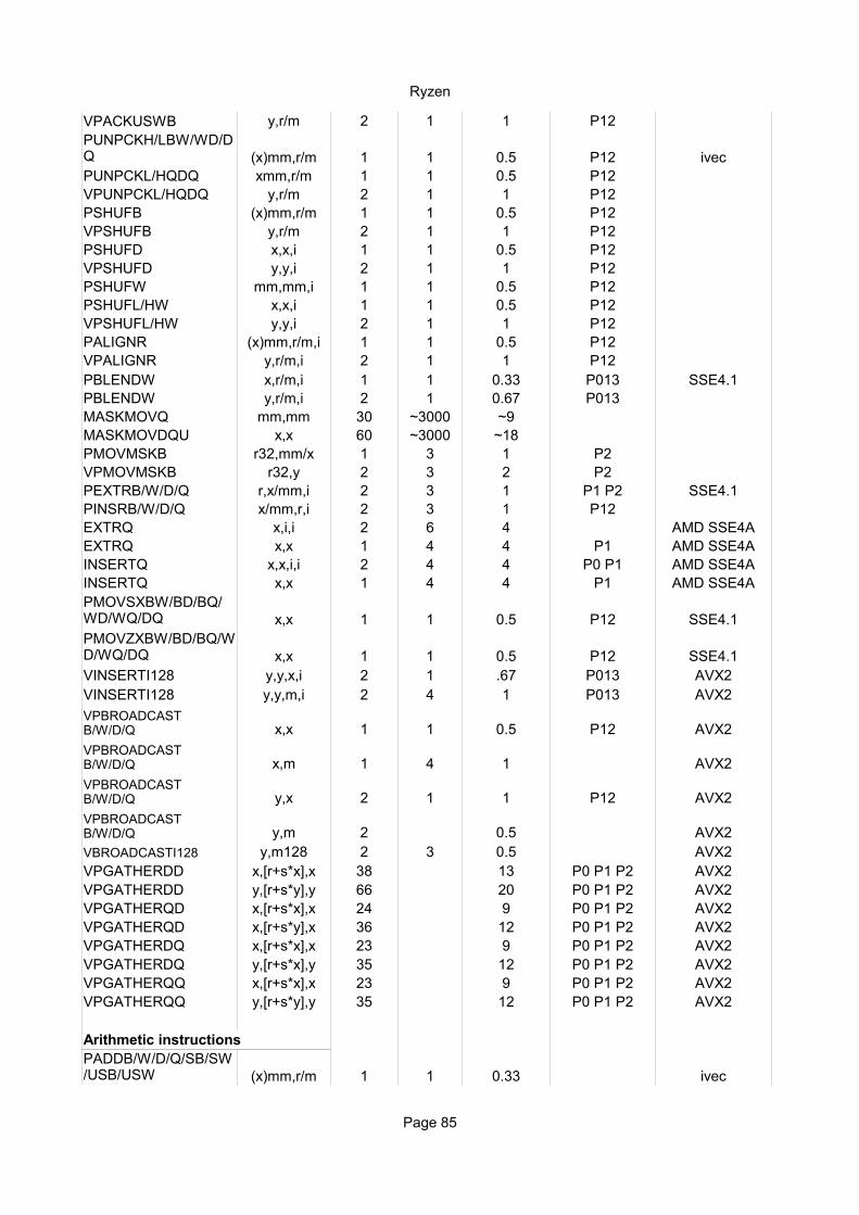
Ryzen
Page 85
VPACKUSWB y,r/m 2 1 1 P12
(x)mm,r/m 1 1 0.5 P12 ivecPUNPCKL/HQDQ xmm,r/m 1 1 0.5 P12VPUNPCKL/HQDQ y,r/m 2 1 1 P12PSHUFB (x)mm,r/m 1 1 0.5 P12VPSHUFB y,r/m 2 1 1 P12PSHUFD x,x,i 1 1 0.5 P12VPSHUFD y,y,i 2 1 1 P12PSHUFW mm,mm,i 1 1 0.5 P12PSHUFL/HW x,x,i 1 1 0.5 P12VPSHUFL/HW y,y,i 2 1 1 P12PALIGNR (x)mm,r/m,i 1 1 0.5 P12VPALIGNR y,r/m,i 2 1 1 P12PBLENDW x,r/m,i 1 1 0.33 P013 SSE4.1PBLENDW y,r/m,i 2 1 0.67 P013MASKMOVQ mm,mm 30 ~3000 ~9MASKMOVDQU x,x 60 ~3000 ~18PMOVMSKB r32,mm/x 1 3 1 P2VPMOVMSKB r32,y 2 3 2 P2PEXTRB/W/D/Q r,x/mm,i 2 3 1 P1 P2 SSE4.1PINSRB/W/D/Q x/mm,r,i 2 3 1 P12EXTRQ x,i,i 2 6 4 AMD SSE4AEXTRQ x,x 1 4 4 P1 AMD SSE4AINSERTQ x,x,i,i 2 4 4 P0 P1 AMD SSE4AINSERTQ x,x 1 4 4 P1 AMD SSE4A
x,x 1 1 0.5 P12 SSE4.1
x,x 1 1 0.5 P12 SSE4.1VINSERTI128 y,y,x,i 2 1 .67 P013 AVX2VINSERTI128 y,y,m,i 2 4 1 P013 AVX2
x,x 1 1 0.5 P12 AVX2
x,m 1 4 1 AVX2
y,x 2 1 1 P12 AVX2
y,m 2 0.5 AVX2VBROADCASTI128 y,m128 2 3 0.5 AVX2VPGATHERDD x,[r+s*x],x 38 13 P0 P1 P2 AVX2VPGATHERDD y,[r+s*y],y 66 20 P0 P1 P2 AVX2VPGATHERQD x,[r+s*x],x 24 9 P0 P1 P2 AVX2VPGATHERQD x,[r+s*y],x 36 12 P0 P1 P2 AVX2VPGATHERDQ x,[r+s*x],x 23 9 P0 P1 P2 AVX2VPGATHERDQ y,[r+s*x],y 35 12 P0 P1 P2 AVX2VPGATHERQQ x,[r+s*x],x 23 9 P0 P1 P2 AVX2VPGATHERQQ y,[r+s*y],y 35 12 P0 P1 P2 AVX2
Arithmetic instructions
(x)mm,r/m 1 1 0.33 ivec
PUNPCKH/LBW/WD/DQ
PMOVSXBW/BD/BQ/WD/WQ/DQ
PMOVZXBW/BD/BQ/WD/WQ/DQ
VPBROADCASTB/W/D/Q
VPBROADCASTB/W/D/Q
VPBROADCASTB/W/D/Q
VPBROADCASTB/W/D/Q
PADDB/W/D/Q/SB/SW/USB/USW
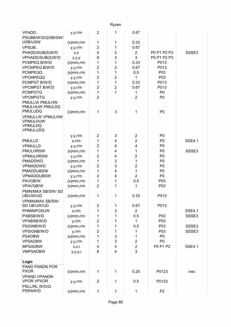
Ryzen
Page 86
VPADD.. y,y,r/m 2 1 0.67
(x)mm,r/m 1 1 0.33VPSUB.. y,y,r/m 2 1 0.67PHADD/SUB(S)W/D x,x 4 2 2 P0 P1 P2 P3 SSSE3VPHADD/SUB(S)W/D y,y,y 8 3 3 P0 P1 P2 P3PCMPEQ B/W/D (x)mm,r/m 1 1 0.33 P013VPCMPEQ B/W/D y,y,r/m 2 2 0.67 P013PCMPEQQ (x)mm,r/m 1 1 0.5 P03VPCMPEQQ y,y,r/m 2 2 1 P03PCMPGT B/W/D (x)mm,r/m 1 1 0.33 P013VPCMPGT B/W/D y,y,r/m 2 2 0.67 P013PCMPGTQ (x)mm,r/m 1 1 1 P0VPCMPGTQ y,y,r/m 2 2 P0
(x)mm,r/m 1 3 1 P0
y,y,r/m 2 3 2 P0PMULLD x,r/m 1 4 2 P0 SSE4.1VPMULLD y,y,r/m 2 4 4 P0PMULHRSW (x)mm,r/m 1 4 1 P0 SSSE3VPMULHRSW y,y,r/m 2 4 2 P0PMADDWD (x)mm,r/m 1 3 1 P0VPMADDWD y,y,r/m 2 3 2 P0PMADDUBSW (x)mm,r/m 1 4 1 P0VPMADDUBSW y,y,r/m 2 4 2 P0PAVGB/W (x)mm,r/m 1 1 0.5 P03VPAVGB/W (x)mm,r/m 2 1 1 P03
(x)mm,r/m 1 1 0.33 P013
y,y,r/m 2 1 0.67 P013PHMINPOSUW x,r/m 1 3 2 SSE4.1PABSB/W/D (x)mm,r/m 1 1 0.5 P03 SSSE3VPABSB/W/D y,r/m 2 1 1 P03PSIGNB/W/D (x)mm,r/m 1 1 0.5 P03 SSSE3VPSIGNB/W/D y,r/m 2 1 1 P03 SSSE3PSADBW (x)mm,r/m 1 3 1 P0VPSADBW y,y,r/m 1 3 2 P0MPSADBW x,x,i 4 4 2 P0 P1 P2 SSE4.1VMPSADBW y,y,y,i 8 4 3
Logic
(x)mm,r/m 1 1 0.25 P0123 ivec
y,y,r/m 2 1 0.5 P0123
(x)mm,r/m 1 1 1 P2
PSUBB/W/D/Q/SB/SW/USB/USW
PMULLW PMULHW PMULHUW PMULDQ PMULUDQ
VPMULLW VPMULHW VPMULHUW VPMULDQ VPMULUDQ
PMIN/MAX SB/SW/ SD UB/UW/UD
VPMIN/MAX SB/SW/ SD UB/UW/UD
PAND PANDN POR PXOR
VPAND VPANDN VPOR VPXOR
PSLL/RL W/D/Q PSRAW/D

Ryzen
Page 87
y,y,x/m 2 1 2 P2
(x)mm,i 1 1 1 P2
y,y,i 2 1 2 P2PSLLDQ, PSRLDQ x,i 1 1 0.5 P12VPSLLDQ VPSRLDQ y,y,i 2 1 1 P12
x,x,x 1 3 2 P1 AVX2
y,y,y 2 3 4 P1 AVX2PTEST x,r/m 1 2 1 P2 SSE4.1VPTEST y,y/m 3 4 2 P1 P2
String instructionsPCMPESTRI x,x,i 6 8 3 P1 P2 SSE4.2PCMPESTRI x,m,i 12 4 SSE4.2PCMPESTRM x,x,i 7 8 3 P0 P1 P2 SSE4.2PCMPESTRM x,m,i 12 4 SSE4.2PCMPISTRI x,x,i 2 11 2 P1 P2 SSE4.2PCMPISTRI x,m,i 3 2 SSE4.2PCMPISTRM x,x,i 3 7 2 P1 P2 SSE4.2PCMPISTRM x,m,i 4 2 SSE4.2
EncryptionPCLMULQDQ x,x/m,i 4 4 2 pclmulAESDEC x,x 1 4 0.5 P01 aesAESDECLAST x,x 1 4 0.5 P01 aesAESENC x,x 1 4 0.5 P01 aesAESENCLAST x,x 1 4 0.5 P01 aesAESIMC x,x 1 4 0.5 P01 aesAESKEYGENASSIST x,x,i 1 4 0.5 P01 aesSHA1RNDS4 x,x,i 1 6 4 P1 shaSHA1NEXTE x,x 1 1 1 P1 shaSHA1MSG1 x,x 2 2 1 multi shaSHA1MSG2 x,x 1 1 0.5 P12 shaSHA256RNDS2 x,x 1 4 2 P1 shaSHA256MSG1 x,x 2 2 0.5 P0123 shaSHA256MSG2 x,x 4 3 2 P0123 sha
OtherEMMS 1 0.25
Floating point XMM and YMM instructionsInstruction Operands Ops Latency Domain, notes
Move instructions
VPSLL/RL W/D/Q VP-SRAW/D
PSLL/RL W/D/Q PSRAW/D
VPSLL/RL W/D/Q VP-SRAW/D
VPSLLVD/QVPSRAVDVPSRLVD/Q
VPSLLVD/QVPSRAVDVPSRLVD/Q
Reciprocal throughput
Execution pipes
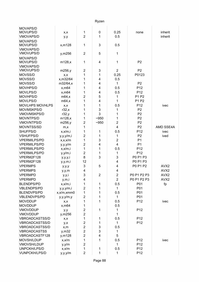
Ryzen
Page 88
x,x 1 0 0.25 none inheritVMOVAPS/D y,y 2 1 0.5 inherit
x,m128 1 3 0.5
y,m256 2 5 1
m128,x 1 4 1 P2
m256,y 2 3 2 P2MOVSS/D x,x 1 1 0.25 P0123MOVSS/D x,m32/64 1 4 0.5MOVSS/D m32/64,x 1 4 1 P2MOVHPS/D x,m64 1 4 0.5 P12MOVLPS/D x,m64 1 4 0.5 P12MOVHPS/D m64,x 2 5 1 P1 P2MOVLPS/D m64,x 1 4 1 P1 P2MOVLHPS MOVHLPS x,x 1 1 0.5 P12 ivecMOVMSKPS/D r32,x 1 3 1 P2VMOVMSKPS/D r32,y 1 3 1 P2MOVNTPS/D m128,x 1 ~950 1 P2VMOVNTPS/D m256,y 2 ~950 2 P2MOVNTSS/SD m,x 1 4 P2 AMD SSE4ASHUFPS/D x,x/m,i 1 1 0.5 P12 ivecVSHUFPS/D y,y,y/m,i 2 1 1 P2 ivedVPERMILPS/PD x,x,x/m 1 3 2 P1VPERMILPS/PD y,y,y/m 2 4 4 P1VPERMILPS/PD x,x/m,i 1 1 0.5 P12VPERMILPS/PD y,y/m,i 2 1 1 P12VPERM2F128 y,y,y,i 8 3 3 P0 P1 P3VPERM2F128 y,y,m,i 12 4 P0 P1 P3VPERMPS y,y,y 3 5 4 P0 P1 P2 AVX2VPERMPS y,y,m 4 4 AVX2VPERMPD y,y,i 3 2 2 P0 P1 P2 P3 AVX2VPERMPD y,m,i 4 2 P0 P1 P2 P3 AVX2BLENDPS/PD x,x/m,i 1 1 0.5 P01 fpVBLENDPS/PD y,y,y/m,i 2 1 1 P01BLENDVPS/PD x,x/m,xmm0 1 1 0.5 P01VBLENDVPS/PD y,y,y/m,y 2 1 1 P01MOVDDUP x,x 1 1 0.5 P12 ivecMOVDDUP x,m64 1 0.5VMOVDDUP y,y 2 1 1 P12VMOVDDUP y,m256 2 1VBROADCASTSS/D x,x 1 1 0.5 P12VBROADCASTSS/D y,x 2 1 1 P12VBROADCASTSS/D x,m 2 3 0.5VBROADCASTSS y,m32 2 3 1VBROADCASTF128 y,m128 2 4 5MOVSH/LDUP x,x/m 1 1 0.5 P12 ivecVMOVSH/LDUP y,y/m 2 1 P12UNPCKH/LPS/D x,x/m 1 1 0.5 P12VUNPCKH/LPS/D y,y,y/m 2 1 1 P12
MOVAPS/D MOVUPS/D
MOVAPS/D MOVUPS/DVMOVAPS/D VMOVUPS/D
MOVAPS/D MOVUPS/DVMOVAPS/D VMOVUPS/D

Ryzen
Page 89
EXTRACTPS r32,x,i 2 3 1 P1 P2EXTRACTPS m32,x,i 2 6 1 P1 P2VEXTRACTF128 x,y,i 1 1 0.33 P013VEXTRACTF128 m128,y,i 2 7 1 P01 P2INSERTPS x,x,i 1 1 0.5 P12 ivecINSERTPS x,m32,i 1 4 1 P12VINSERTF128 y,y,x,i 2 1 0.5 P013VINSERTF128 y,y,m128,i 2 5 1 P013VMASKMOVPS/D x,x,m128 1 4 1 P01VMASKMOVPS/D y,y,m256 2 4 1 P01VMASKMOVPS/D m128,x,x 19 ~50 5 P1 P2VMASKMOVPS/D m256,y,y 42 ~50 11 P1 P2VGATHERDPS x,[r+s*x],x 38 13 P0 P1 P2 AVX2VGATHERDPS y,[r+s*y],y 66 20 P0 P1 P2 AVX2VGATHERQPS x,[r+s*x],x 24 9 P0 P1 P2 AVX2VGATHERQPS x,[r+s*y],x 36 12 P0 P1 P2 AVX2VGATHERDPD x,[r+s*x],x 23 9 P0 P1 P2 AVX2VGATHERDPD y,[r+s*x],y 35 12 P0 P1 P2 AVX2VGATHERQPD x,[r+s*x],x 23 9 P0 P1 P2 AVX2VGATHERQPD y,[r+s*y],y 35 12 P0 P1 P2 AVX2
ConversionCVTPD2PS x,x 1 3 1 P3 fpVCVTPD2PS x,y 2 5 2 P3CVTPS2PD x,x 1 3 1 P3VCVTPS2PD y,x 2 5 2 P3CVTSD2SS x,x 1 3 1 P3CVTSS2SD x,x 1 3 1 P3CVTDQ2PS x,x 1 4 1 P3VCVTDQ2PS y,y 2 4 2 P3CVT(T) PS2DQ x,x 1 4 1 P3 mixed domainVCVT(T) PS2DQ y,y 2 4 2 P3CVTDQ2PD x,x 2 6 1 P12 P3VCVTDQ2PD y,x 4 6 2 P12 P3CVT(T)PD2DQ x,x 2 6 1 P12 P3VCVT(T)PD2DQ x,y 4 6 2 P12 P3CVTPI2PS x,mm 2 6 1 P12 P3CVT(T)PS2PI mm,x 2 6 1 P12 P3CVTPI2PD x,mm 2 6 1 P12 P3CVT(T) PD2PI mm,x 2 6 1 P12 P3CVTSI2SS x,r32 2 8 1CVT(T)SS2SI r32,x 2 7 1 P2 P3CVTSI2SD x,r32/64 2 8 1CVT(T)SD2SI r32/64,x 2 7 1 P2 P3VCVTPS2PH x/m,x,i 2 6 2 P1 P3VCVTPS2PH x/m,y,i 4 6 2 P12 P3VCVTPH2PS x,x/m 2 6 2 P1 P3VCVTPH2PS y,x/m 4 6 2 P12 P3
ArithmeticADDSS/D SUBSS/D x,x/m 1 3 0.5 P23 fpADDPS/D SUBPS/D x,x/m 1 3 0.5 P23 fp

Ryzen
Page 90
VADDPS/D VSUBPS/D y,y,y/m 2 3 1 P23 fpADDSUBPS/D x,x/m 1 3 0.5 P23 fpVADDSUBPS/D y,y,y/m 2 3 1 P23
HADDPS/D HSUBPS/D x,x 4 7 2 P1 P2 P3
y,y,y/m 8 7 3 P1 P2 P3 mixed domainMULSS MULPS x,x/m 1 3 0.5 P01 fpMULSD MULPD x,x/m 1 4 0.5 P01 fpVMULPS y,y,y/m 2 3 1 P01 fpVMULPD y,y,y/m 2 4 1 P01 fpDIVSS DIVPS x,x/m 1 10 3 P3VDIVPS y,y,y/m 2 10 6 P3DIVSD DIVPD x,x/m 1 8-13 4-5 P3VDIVPD y,y,y/m 2 8-13 8-9 P3RCPSS/PS x,x/m 1 5 1 P01VRCPPS y,y/m 2 5 2 P01
x,x/m 1 1 0.5 P01VCMPPS/D y,y,y/m 2 1 1 P01
x,x/m 2 4 1 P012
x,x/m 1 1 0.5 P01 fpVMAXPS/D VMINPS/D y,y,y/m 2 1 1 P01ROUNDSS/SD/PS/PD x,x/m,i 1 4 1 P3 fp
y,y/m,i 2 4 2 P3 fpDPPS x,x,i 8 15 4 P0 P1 P2 P3 SSE4.1DPPS x,m,i 10 5 P0 P1 P2 P3 SSE4.1VDPPS y,y,y,i 13 16 5 P0 P1 P2 P3 SSE4.1VDPPS y,m,i 14 5 P0 P1 P2 P3 SSE4.1DPPD x,x,i 3 10 3 P0 P1 P2 P3 SSE4.1DPPD x,m,i 5 4 P0 P1 P2 P3 SSE4.1VFMADD132SS/SD x,x,x/m 1 5 0.5 P01 FMA3VFMADD132PS/PD x,x,x/m 1 5 0.5 P01 FMA3VFMADD132PS/PD y,y,y/m 2 5 1 P01 FMA3All other FMA3 instructions: same as above P01 FMA3VFMADDSS/SD x,x,x,x/m 1 5 0.5 P01VFMADDPS/PD x,x,x,x/m 1 5 0.5 P01VFMADDPS/PD y,y,y,y/m 2 5 1 P01All other FMA4 instructions: same as above
MathSQRTSS/PS x,x/m 1 9-10 4-5 P3 fpVSQRTPS y,y/m 2 9-10 8-10SQRTSD/PD x,x/m 1 14-15 4-8VSQRTPD y,y/m 2 14-15 8-16RSQRTSS/PS x,x/m 1 5 1 P01VRSQRTPS y,y/m 2 5 2 P01
Logic
VHADDPS/DVHSUBPS/D
CMPSS/DCMPPS/D
COMISS/D UCOMISS/D
MAXSS/SD/PS/PD MINSS/SD/PS/PD
VROUNDSS/SD/PS/ PD
Not officially supported.Don't use!

Ryzen
Page 91
x,x/m 1 1 0.25 P0123 fp
y,y,y/m 2 1 0.5 P0123
OtherVZEROUPPER 10 4 32 bit modeVZEROUPPER 17 6 64 bit modeVZEROALL 18 6 32 bit modeVZEROALL 33 11 64 bit modeLDMXCSR m32 1 16STMXCSR m32 2 14FXSAVE m4096 87 90FXRSTOR m4096 121 140XSAVE m 160 166XSAVEOPT m 97 130XRSTOR m 213 340XSAVEC m 111 150
AND/ANDN/OR/XORPS/ PD
VAND/ANDN/OR/XORPS/PD

Bobcat
Page 92
AMD BobcatList of instruction timings and macro-operation breakdown
Explanation of column headings:Instruction:
Operands:
Ops:
Latency:
Execution pipe:
Integer instructionsInstruction Operands Ops Latency Notes
Move instructionsMOV r,r 1 1 0.5 I0/1MOV r,i 1 0.5 I0/1MOV r,m 1 4 1 AGU Any addr. modeMOV m,r 1 4 1 AGU Any addr. modeMOV m8,r8H 1 7 1 AGU AH, BH, CH, DHMOV m,i 1 1 AGUMOVNTI m,r 1 6 1 AGUMOVZX, MOVSX r,r 1 1 0.5 I0/1MOVZX, MOVSX r,m 1 5 1MOVSXD r64,r32 1 1 0.5MOVSXD r64,m32 1 5 1CMOVcc r,r 1 1 0.5 I0/1CMOVcc r,m 1 1XCHG r,r 2 1 1 I0/1XCHG r,m 3 20 Timing dep. on hw
Instruction name. cc means any condition code. For example, Jcc can be JB, JNE, etc.
i = immediate constant, r = any register, r32 = 32-bit register, etc., mm = 64 bit mmx register, xmm = 128 bit xmm register, m = any memory operand including indirect operands, m64 means 64-bit memory operand, etc.
Number of micro-operations issued from instruction decoder to schedulers. In-structions with more than 2 micro-operations are micro-coded.
This is the delay that the instruction generates in a dependency chain. The num-bers are minimum values. Cache misses, misalignment, and exceptions may in-crease the clock counts considerably. Floating point operands are presumed to be normal numbers. Denormal numbers, NAN's, infinity and exceptions increase the delays. The latencies listed do not include memory operands where the oper-and is listed as register or memory (r/m).
The clock frequency varies dynamically, which makes it difficult to measure la-tencies. The values listed are measured after the execution of millions of similar instructions, assuming that this will make the processor boost the clock frequency to the highest possible value.
Reciprocal through-put:
This is also called issue latency. This value indicates the average number of clock cycles from the execution of an instruction begins to a subsequent inde-pendent instruction of the same kind can begin to execute. A value of 1/2 indi-cates that the execution units can handle 2 instructions per clock cycle in one thread. However, the throughput may be limited by other bottlenecks in the pipe-line.
Indicates which execution pipe is used for the micro-operations. I0 means integer pipe 0. I0/1 means integer pipe 0 or 1. FP0 means floating point pipe 0 (ADD). FP1 means floating point pipe 1 (MUL). FP0/1 means either one of the two float-ing point pipes. Two micro-operations can execute simultaneously if they go to different execution pipes.
Reciprocal throughput
Execution pipe

Bobcat
Page 93
XLAT 2 5PUSH r 1 1PUSH i 1 1PUSH m 3 2PUSHF(D/Q) 9 6PUSHA(D) 9 9POP r 1 1POP m 4 4POPF(D/Q) 29 22POPA(D) 9 8LEA r16,[m] 2 3 2 I0 Any address sizeLEA r32/64,[m] 1 1 0.5 I0/1 no scale, no offsetLEA r32/64,[m] 1 2-4 1 I0 w. scale or offsetLEA r64,[m] 1 0.5 I0/1 RIP relativeLAHF 4 4 2SAHF 1 1 0.5 I0/1SALC 1 1BSWAP r 1 1 0.5 I0/1PREFETCHNTA m 1 1 AGUPREFETCHT0/1/2 m 1 1 AGUPREFETCH m 1 1 AGU AMD onlySFENCE 4 ~45 AGULFENCE 1 1 AGUMFENCE 4 ~45 AGU
Arithmetic instructionsADD, SUB r,r/i 1 1 0.5 I0/1ADD, SUB r,m 1 1ADD, SUB m,r 1 1ADC, SBB r,r/i 1 1 1 I0/1ADC, SBB r,m 1 1ADC, SBB m,r/i 1 6-7CMP r,r/i 1 1 0.5 I0/1CMP r,m 1 1INC, DEC, NEG r 1 1 0.5 I0/1INC, DEC, NEG m 1 6AAA 9 5AAS 9 10DAA 12 7DAS 16 8AAD 4 5AAM 33 23 23MUL, IMUL r8/m8 1 3 1 I0MUL, IMUL r16/m16 3 3-5 I0 latency ax=3, dx=5MUL, IMUL r32/m32 2 3-4 2 I0 latency eax=3, edx=4
MUL, IMUL r64/m64 2 6-7 I0 latency rax=6, rdx=7IMUL r16,r16/m16 1 3 1 I0IMUL r32,r32/m32 1 3 1 I0IMUL r64,r64/m64 1 6 4 I0IMUL r16,(r16),i 2 4 3 I0IMUL r32,(r32),i 1 3 1 I0IMUL r64,(r64),i 1 7 4 I0DIV r8/m8 1 27 27 I0

Bobcat
Page 94
DIV r16/m16 1 33 33 I0DIV r32/m32 1 49 49 I0DIV r64/m64 1 81 81 I0IDIV r8/m8 1 29 29 I0IDIV r16/m16 1 37 37 I0IDIV r32/m32 1 55 55 I0IDIV r64/m64 1 81 81 I0CBW, CWDE, CDQE 1 1 I0/1CWD, CDQ, CQO 1 1 I0/1
Logic instructionsAND, OR, XOR r,r 1 1 0.5 I0/1AND, OR, XOR r,m 1 1AND, OR, XOR m,r 1 1TEST r,r 1 1 0.5 I0/1TEST r,m 1 1NOT r 1 1 0.5 I0/1NOT m 1 1SHL, SHR, SAR r,i/CL 1 1 0.5 I0/1ROL, ROR r,i/CL 1 1 0.5 I0/1RCL, RCR r,1 1 1 1 I0/1RCL r,i 9 5 5RCR r,i 7 4 4RCL r,CL 9 6 5RCR r,CL 9 5 4
m,i /CL 1 7 1RCL, RCR m,1 1 7 1RCL m,i 10 ~15RCR m,i 9 18 ~14RCL m,CL 9 15RCR m,CL 8 15SHLD, SHRD r,r,i 6 3 3SHLD, SHRD r,r,cl 7 4 4SHLD, SHRD m,r,i/CL 8 18 15BT r,r/i 1 0.5BT m,i 1 1BT m,r 5 3BTC, BTR, BTS r,r/i 2 2 1BTC m,i 5 15BTR, BTS m,i 4-5 15BTC m,r 8 16 13BTR, BTS m,r 8 15 15BSF, BSR r,r 11 6 6BSF, BSR r,m 11 6POPCNT r,r/m 9 12 5 SSE4.A/SSE4.2LZCNT r,r/m 8 5 SSE4.A, AMD onlySETcc r 1 1 0.5SETcc m 1 1CLC, STC 1 0.5 I0/1CMC 1 1 0.5 I0/1CLD 1 1 I0STD 2 2 I0,I1
SHL,SHR,SAR,ROL, ROR

Bobcat
Page 95
Control transfer instructionsJMP short/near 1 2JMP r 1 2JMP m(near) 1 2Jcc short/near 1 1/2 - 2 recip. t. = 2 if jumpJ(E/R)CXZ short 2 1 - 2 recip. t. = 2 if jumpLOOP short 8 4CALL near 2 2CALL r 2 2CALL m(near) 5 2RET 1 ~3RET i 4 ~4BOUND m 8 4 values for no jumpINTO 4 2 values for no jump
String instructionsLODS 4 ~3REP LODS 5 ~3 values are per countSTOS 4 2REP STOS 2 best case 6-7 B/clkMOVS 7 5REP MOVS 2 best case 5 B/clkSCAS 5 3REP SCAS 6 3 values are per countCMPS 7 4REP CMPS 6 3 values are per count
OtherNOP (90) 1 0 0.5 I0/1Long NOP (0F 1F) 1 0 0.5 I0/1PAUSE 6 6ENTER i,0 12 36ENTER a,b 10+6b 34+6bLEAVE 2 3 32 bit modeCPUID 30-52 70-830RDTSC 26 87RDPMC 14 8
Floating point x87 instructionsInstruction Operands Ops Latency Notes
Move instructionsFLD r 1 2 0.5 FP0/1FLD m32/64 1 6 1 FP0/1FLD m80 7 14 5FBLD m80 21 30 35FST(P) r 1 2 0.5 FP0/1FST(P) m32/64 1 6 1 FP1FSTP m80 16 19 9FBSTP m80 217 177 180FXCH r 1 0 1 FP1
Reciprocal throughput
Execution pipe

Bobcat
Page 96
FILD m 1 9 1 FP1FIST(T)(P) m 1 6 1FLDZ, FLD1 1 1 FP1FCMOVcc st0,r 12 7 7 FP0/1FFREE r 1 1 FP1FINCSTP, FDECSTP 1 1 1 FP1FNSTSW AX 2 ~20 10 FP1FNSTSW m16 2 ~20 10 FP1FNSTCW m16 3 2 FP0FLDCW m16 12 10 FP1
Arithmetic instructionsFADD(P),FSUB(R)(P) r 1 3 1 FP0FADD(P),FSUB(R)(P) m 1 3 1 FP0FIADD,FISUB(R) m 2 3 FP0,FP1FMUL(P) r 1 5 3 FP1FMUL(P) m 1 5 3 FP1FIMUL m 2 FP1FDIV(R)(P) r 1 19 19 FP1FDIV(R)(P) m 1 19 FP1FIDIV(R) m 2 19 FP1FABS, FCHS 1 2 2 FP1FCOM(P), FUCOM(P) r 1 1 FP0FCOM(P), FUCOM(P) m 1 1 FP0FCOMPP, FUCOMPP 1 1 FP0FCOMI(P) r 1 2 2 FP0FICOM(P) m 2 1 FP0, FP1FTST 1 1 FP0FXAM 2 2 FP1FRNDINT 5 11 FP0, FP1FPREM 1 11-16 FP1FPREM1 1 11-19 FP1
MathFSQRT 1 31 FP1FLDPI, etc. 1 1 FP0FSIN 4-44 27-105 27-105 FP0, FP1FCOS 11-51 51-94 51-94 FP0, FP1FSINCOS 11-75 48-110 48-110 FP0, FP1FPTAN ~45 ~113 ~113 FP0, FP1FPATAN 9-75 49-163 49-163 FP0, FP1FSCALE 5 8 FP0, FP1FXTRACT 7 9 FP0, FP1F2XM1 30-56 ~60 FP0, FP1FYL2X 8 29 FP0, FP1FYL2XP1 12 44 FP0, FP1
OtherFNOP 1 0 0.5 FP0, FP1(F)WAIT 1 0 0.5 ALUFNCLEX 9 30 FP0, FP1FNINIT 26 78 FP0, FP1FNSAVE m 85 163 FP0, FP1

Bobcat
Page 97
FRSTOR m 80 123 FP0, FP1FXSAVE m 71 105 FP0, FP1FXRSTOR m 111 118 FP0, FP1
Integer MMX and XMM instructionsInstruction Operands Ops Latency Notes
Move instructionsMOVD r32, mm 1 7 1 FP0MOVD mm, r32 1 7 3 FP0/1MOVD mm,m32 1 5 1 FP0/1MOVD r32, xmm 1 6 1 FP0MOVD xmm, r32 3 6 3 FP1MOVD xmm,m32 2 5 1 FP1MOVD m32,(x)mm 1 6 2 FP1
MOVD (MOVQ) r64,(x)mm 1 7 1 FP0MOVD (MOVQ) mm,r64 2 7 3 FP0/1 do.MOVD (MOVQ) xmm,r64 3 7 3 FP0/1 do.MOVQ mm,mm 1 1 0.5 FP0/1MOVQ xmm,xmm 2 1 1 FP0/1MOVQ mm,m64 1 5 1 FP0/1MOVQ xmm,m64 2 5 1 FP1MOVQ m64,(x)mm 1 6 2 FP1MOVDQA xmm,xmm 2 1 1 FP0/1MOVDQA xmm,m 2 6 2 AGUMOVDQA m,xmm 2 6 3 FP1MOVDQU, LDDQU xmm,m 2 6-9 2-5.5 AGUMOVDQU m,xmm 2 6-9 3-6 FP1MOVDQ2Q mm,xmm 1 1 0.5 FP0/1MOVQ2DQ xmm,mm 2 1 1 FP0/1MOVNTQ m,mm 1 13 1,5 FP1MOVNTDQ m,xmm 2 13 3 FP1
mm,r/m 1 1 0.5 FP0/1
xmm,r/m 3 2 2 FP0/1
mm,r/m 1 1 0.5
xmm,r/m 2 1 1PUNPCKHQDQ xmm,r/m 2 1 1 FP0, FP1PUNPCKLQDQ xmm,r/m 1 1 0.5 FP0/1PSHUFB mm,mm 1 2 1 FP0/1 Suppl. SSE3PSHUFB xmm,xmm 6 3 3 FP0/1 Suppl. SSE3PSHUFD xmm,xmm,i 3 2 2 FP0/1PSHUFW mm,mm,i 1 1 0.5 FP0/1PSHUFL/HW xmm,xmm,i 2 2 2 FP0/1PALIGNR xmm,xmm,i 20 19 12 FP0/1 Suppl. SSE3MASKMOVQ mm,mm 32 146-1400 130-1170 FP0, FP1MASKMOVDQU xmm,xmm 64 279-3000 260-2300 FP0, FP1PMOVMSKB r32,(x)mm 1 8 2 FP0
Reciprocal throughput
Execution pipe
Moves 64 bits. Name differs
PACKSSWB/DW PACKUSWB
PACKSSWB/DW PACKUSWB
PUNPCKH/LBW/WD/DQ
PUNPCKH/LBW/WD/DQ

Bobcat
Page 98
PEXTRW r32,(x)mm,i 2 12 2 FP0, FP1PINSRW mm,r32,i 2 10 6 FP0/1PINSRW xmm,r32,i 3 10 FP0/1INSERTQ xmm,xmm 3 3-4 3 FP0, FP1 SSE4.A, AMD onlyINSERTQ xmm,xmm,i,i 3 3-4 3 FP0, FP1 SSE4.A, AMD onlyEXTRQ xmm,xmm 1 1 1 FP0/1 SSE4.A, AMD onlyEXTRQ xmm,xmm,i,i 1 2 2 FP0/1 SSE4.A, AMD only
Arithmetic instructions
mm,r/m 1 1 0.5 FP0/1
xmm,r/m 2 1 1 FP0/1PHADD/SUBW/SW/D mm,r/m 1 1 0.5 FP0/1 Suppl. SSE3PHADD/SUBW/SW/D xmm,r/m 2 4 1 FP0/1 Suppl. SSE3PCMPEQ/GT B/W/D mm,r/m 1 1 0.5 FP0/1PCMPEQ/GT B/W/D xmm,r/m 2 1 1 FP0/1
mm,r/m 1 2 1 FP0
xmm,r/m 2 2 2 FP0PMULHRSW mm,r/m 1 2 1 FP0 Suppl. SSE3PMULHRSW xmm,r/m 2 2 2 FP0 Suppl. SSE3PMADDWD mm,r/m 1 2 1 FP0PMADDWD xmm,r/m 2 2 2 FP0PMADDUBSW mm,r/m 1 2 1 FP0 Suppl. SSE3PMADDUBSW xmm,r/m 2 2 2 FP0 Suppl. SSE3PAVGB/W mm,r/m 1 1 0.5 FP0/1PAVGB/W xmm,r/m 2 1 1 FP0/1PMIN/MAX SW/UB mm,r/m 1 1 0.5 FP0/1PMIN/MAX SW/UB xmm,r/m 2 1 1 FP0/1PABSB/W/D mm,r/m 1 1 0.5 FP0/1 Suppl. SSE3PABSB/W/D xmm,r/m 2 1 1 FP0/1 Suppl. SSE3PSIGNB/W/D mm,r/m 1 1 0.5 FP0/1 Suppl. SSE3PSIGNB/W/D xmm,r/m 2 1 1 FP0/1 Suppl. SSE3PSADBW mm,r/m 1 2 2 FP0PSADBW xmm,r/m 2 2 2 FP0, FP1
Logic
mm,r/m 1 1 0.5 FP0/1
xmm,r/m 2 1 1 FP0/1
PADDB/W/D/Q PADDSB/W PADDUSB/W PSUBB/W/D/Q PSUBSB/W PSUBUSB/W
PADDB/W/D/Q PADDSB/W ADDUSB/W PSUBB/W/D/Q PSUBSB/W PSUBUSB/W
PMULLW PMULHW PMULHUW PMULUDQ
PMULLW PMULHW PMULHUW PMULUDQ
PAND PANDN POR PXOR
PAND PANDN POR PXOR

Bobcat
Page 99
mm,i/mm/m 1 1 1 FP0/1
xmm,i/xmm/m 2 1 1 FP0/1PSLLDQ, PSRLDQ xmm,i 2 1 1 FP0/1
OtherEMMS 1 0.5 FP0/1
Floating point XMM instructionsInstruction Operands Ops Latency Notes
Move instructionsMOVAPS/D r,r 2 1 1 FP0/1MOVAPS/D r,m 2 6 2 AGUMOVAPS/D m,r 2 6 3 FP1MOVUPS/D r,r 2 1 1 FP0/1MOVUPS/D r,m 2 6-9 2-6 AGUMOVUPS/D m,r 2 6-9 3-6 FP1MOVSS/D r,r 1 1 0.5 FP0/1MOVSS/D r,m 2 6 2 FP1MOVSS/D m,r 1 5 2 FP1MOVHLPS, MOVLHPS
r,r 1 1 0.5 FP0/1
r,m 1 6 2 AGU
m,r 1 5 3 FP1MOVNTPS/D m,r 2 12 3 FP1MOVNTSS/D m,r 1 12 2 FP1 SSE4.A, AMD onlyMOVDDUP r,r 2 2 1 FP0/1 SSE3MOVDDUP r,m64 2 7 2 FP0/1 SSE3
r,r 2 1 1 FP0/1
r,m 2 12 3 AGUMOVMSKPS/D r32,r 1 ~6 2 FP0SHUFPS/D r,r/m,i 3 2 2 FP0/1UNPCK H/L PS/D r,r/m 2 1 1 FP0/1
ConversionCVTPS2PD r,r/m 2 5 2 FP1CVTPD2PS r,r/m 4 5 3 FP0, FP1CVTSD2SS r,r/m 3 5 3 FP0, FP1CVTSS2SD r,r/m 1 4 1 FP1CVTDQ2PS r,r/m 2 4 4 FP1CVTDQ2PD r,r/m 2 5 2 FP1CVT(T)PS2DQ r,r/m 2 4 4 FP1CVT(T)PD2DQ r,r/m 4 6 3 FP0, FP1CVTPI2PS xmm,mm 1 4 2 FP1CVTPI2PD xmm,mm 2 5 2 FP1CVT(T)PS2PI mm,xmm 1 4 1 FP1
PSLL/RL W/D/Q PSRAW/D
PSLL/RL W/D/Q PSRAW/D
Reciprocal throughput
Execution pipe
MOVHPS/D, MOVLPS/D
MOVHPS/D, MOVLPS/D
MOVSHDUP, MOVSLDUP
MOVSHDUP, MOVSLDUP

Bobcat
Page 100
CVT(T)PD2PI mm,xmm 3 6 2 FP0, FP1CVTSI2SS xmm,r32 3 12 3 FP0, FP1CVTSI2SD xmm,r32 2 11 3 FP1CVT(T)SS2SI r32,xmm 2 12 1 FP0, FP1CVT(T)SD2SI r32,xmm 2 11 1 FP0, FP1
ArithmeticADDSS/D SUBSS/D r,r/m 1 3 1 FP0ADDPS/D SUBPS/D r,r/m 2 3 2 FP0ADDSUBPS/D r,r/m 2 3 2 FP0 SSE3
r,r/m 2 3 2 FP0 SSE3MULSS r,r/m 1 2 1 FP1MULSD r,r/m 1 4 2 FP1MULPS r,r/m 2 2 2 FP1MULPD r,r/m 2 4 4 FP1DIVSS r,r/m 1 13 13 FP1DIVPS r,r/m 2 38 38 FP1DIVSD r,r/m 1 17 17 FP1DIVPD r,r/m 2 34 34 FP1RCPSS r,r/m 1 3 1 FP1RCPPS r,r/m 2 3 2 FP1MAXSS/D MINSS/D r,r/m 1 2 1 FP0MAXPS/D MINPS/D r,r/m 2 2 2 FP0CMPccSS/D r,r/m 1 2 1 FP0CMPccPS/D r,r/m 2 2 2 FP0
r,r/m 1 1 FP0
Logic
r,r/m 2 1 1 FP0/1
MathSQRTSS r,r/m 1 14 14 FP1SQRTPS r,r/m 2 48 48 FP1SQRTSD r,r/m 1 24 24 FP1SQRTPD r,r/m 2 48 48 FP1RSQRTSS r,r/m 1 3 1 FP1RSQRTPS r,r/m 2 3 2 FP1
OtherLDMXCSR m 12 10 FP0, FP1STMXCSR m 3 11 FP0, FP1
HADDPS/D HSUBPS/D
COMISS/D UCOMISS/D
ANDPS/D ANDNPS/D ORPS/D XORPS/D

Jaguar
Page 101
AMD JaguarList of instruction timings and macro-operation breakdown
Explanation of column headings:Instruction:
Operands:
Ops:
Latency:
Execution pipe:
Integer instructionsInstruction Operands Ops Latency Notes
Move instructionsMOV r,r 1 1 0.5 I0/1MOV r,i 1 0.5 I0/1
MOV r8/16,m 1 4 1 AGU
MOV m,r8/16 1 4 1 AGU
MOV r32/64,m 1 3 1 AGU
MOV m,r32/64 1 0 1 AGUMOV m,i 1 1 AGUMOVNTI m,r 1 6 1 AGUMOVZX, MOVSX r,r 1 1 0.5 I0/1MOVZX, MOVSX r,m 1 4 1MOVSXD r64,r32 1 1 0.5
Instruction name. cc means any condition code. For example, Jcc can be JB, JNE, etc.
i = immediate constant, r = any register, r32 = 32-bit register, etc., mm = 64 bit mmx register, xmm = 128 bit xmm register, m = any memory operand including indirect operands, m64 means 64-bit memory operand, etc.
Number of micro-operations issued from instruction decoder to schedulers. In-structions with more than 2 micro-operations are micro-coded.
This is the delay that the instruction generates in a dependency chain. The num-bers are minimum values. Cache misses, misalignment, and exceptions may in-crease the clock counts considerably. Floating point operands are presumed to be normal numbers. Denormal numbers, NAN's, infinity and exceptions increase the delays. The latencies listed do not include memory operands where the oper-and is listed as register or memory (r/m).
The clock frequency varies dynamically, which makes it difficult to measure laten-cies. The values listed are measured after the execution of millions of similar in-structions, assuming that this will make the processor boost the clock frequency to the highest possible value.
Reciprocal through-put:
This is also called issue latency. This value indicates the average number of clock cycles from the execution of an instruction begins to a subsequent independent instruction of the same kind can begin to execute. A value of 1/2 indicates that the execution units can handle 2 instructions per clock cycle in one thread. How-ever, the throughput may be limited by other bottlenecks in the pipeline.
Indicates which execution pipe is used for the micro-operations. I0 means integer pipe 0. I0/1 means integer pipe 0 or 1. FP0 means floating point pipe 0 (ADD). FP1 means floating point pipe 1 (MUL). FP0/1 means either one of the two float-ing point pipes. Two micro-operations can execute simultaneously if they go to different execution pipes.
Reciprocal throughput
Execution pipe
Any addressing mode
Any addressing mode
Any addressing mode
Any addressing mode

Jaguar
Page 102
MOVSXD r64,m32 1 3 1CMOVcc r,r 1 1 0.5 I0/1CMOVcc r,m 1 1XCHG r8,r8 3 2 2 I0/1XCHG r,r 2 1 1 I0/1
XCHG r,m 3 16XLAT 2 5 3PUSH r 1 1PUSH i 1 1PUSH m 2 1PUSH SP 2 1PUSHF(D/Q) 9 6PUSHA(D) 9 8POP r 1 1POP m 3 2POP SP 1 2POPF(D/Q) 29 18POPA(D) 9 8LEA r16,[m] 2 3 2 I0 Any address sizeLEA r32/64,[m] 1 1 0.5 I0/1 1-2 comp., no scaleLEA r32/64,[m] 1 2 1 I0 3 comp. or scaleLEA r64,[m] 1 0.5 I0/1 RIP relativeLAHF 4 3 2SAHF 1 1 0.5 I0/1SALC 1 1 1BSWAP r 1 1 0.5 I0/1MOVBE r,m 1 1 MOVBEMOVBE m,r 1 1 MOVBEPREFETCHNTA m 1 ~100 AGUPREFETCHT0/1/2 m 1 ~100 AGUPREFETCHW m 1 ~100 AGULFENCE 1 0.5 AGUMFENCE 4 ~45 AGUSFENCE 4 ~45 AGU
Arithmetic instructionsADD, SUB r,r/i 1 1 0.5 I0/1ADD, SUB r,m 1 1ADD, SUB m,r 1 6 1ADC, SBB r,r/i 1 1 1 I0/1ADC, SBB r,m 1 1ADC, SBB m,r/i 1 8CMP r,r/i 1 1 0.5 I0/1CMP r,m 1 1INC, DEC, NEG r 1 1 0.5 I0/1INC, DEC, NEG m 1 6 1AAA 9 5AAS 9 8DAA 12 6DAS 16 8AAD 4 5AAM 8 14 13
Timing depends on hw

Jaguar
Page 103
MUL, IMUL r8/m8 1 3 1 I0MUL, IMUL r16/m16 3 3 3 I0MUL, IMUL r32/m32 2 3 2 I0MUL, IMUL r64/m64 2 6 5 I0IMUL r16,r16/m16 1 3 1 I0IMUL r32,r32/m32 1 3 1 I0IMUL r64,r64/m64 1 6 4 I0IMUL r16,(r16),i 2 4 1 I0IMUL r32,(r32),i 1 3 1 I0IMUL r64,(r64),i 1 6 4 I0DIV r8/m8 1 11-14 11-14 I0DIV r16/m16 2 12-19 12-19 I0DIV r32/m32 2 12-27 12-27 I0DIV r64/m64 2 12-43 12-43 I0IDIV r8/m8 1 11-14 11-14 I0IDIV r16/m16 2 12-19 12-19 I0IDIV r32/m32 2 12-27 12-27 I0IDIV r64/m64 2 12-43 12-43 I0CBW, CWDE, CDQE 1 1 I0/1CWD, CDQ, CQO 1 1 I0/1
Logic instructionsAND, OR, XOR r,i 1 1 0.5 I0/1AND, OR, XOR r,r 1 1 0.5 I0/1AND, OR, XOR r,m 1 1AND, OR, XOR m,r 1 6 1ANDN r,r,r 1 1 0.5 BMI1ANDN r,r,m 2 1 BMI1TEST r,i 1 1 0.5 I0/1TEST r,r 1 1 0.5 I0/1TEST r,m 1 1NOT r 1 1 0.5 I0/1NOT m 1 6 1SHL, SHR, SAR r,i/CL 1 1 0.5 I0/1ROL, ROR r,i/CL 1 1 0.5 I0/1RCL, RCR r,1 1 1 1 I0/1RCL r,i 9 5 5RCR r,i 7 4 4RCL r,CL 9 5 5RCR r,CL 7 4 4
m,i /CL 1 6 1RCL, RCR m,1 1 1RCL m,i 10 11RCR m,i 9 11RCL m,CL 9 11RCR m,CL 8 11SHLD, SHRD r,r,i 6 3 3SHLD, SHRD r,r,cl 7 4 4SHLD, SHRD m,r,i/CL 8 11BT r,r/i 1 0.5BT m,i 1 1BT m,r 5 3
SHL,SHR,SAR,ROL, ROR

Jaguar
Page 104
BTC, BTR, BTS r,r/i 2 2 1BTC m,i 5 11BTR, BTS m,i 4 11BTC, BTR, BTS m,r 8 11BSF r,r 7 4 4BSR r,r 8 4 4BSF, BSR r,m 8 4POPCNT r,r/m 1 1 0.5 SSE4A/SSE4.2LZCNT r,r 1 1 0.5 SSE4A/LZCNTTZCNT r,r 2 2 1 BMI1BLSI BLSR r,r 2 2 1 BMI1BLSI BLSR r,m 3 2 BMI1BLSMSK r,r 2 2 1 BMI1BLSMSK r,m 3 2 BMI1BEXTR r,r,r 1 1 0.5 BMI1BEXTR r,m,r 2 1 BMI1SETcc r 1 1 0.5SETcc m 1 1CLC, STC 1 0.5 I0/1CMC 1 1 I0/1CLD 1 1 I0STD 2 2 I0,I1
Control transfer instructionsJMP short/near 1 2JMP r 1 2JMP m(near) 1 2Jcc short/near 1 0.5 - 2 2 if jumpingJ(E/R)CXZ short 2 1 - 2 2 if jumpingLOOP short 8 5LOOPE LOOPNE short 10 6CALL near 2 2CALL r 2 2CALL m(near) 5 2RET 1 3RET i 4 3
BOUND m 8 4
INTO 4 2
String instructionsLODS 4 2REP LODS ~5n ~3nSTOS 4 2REP STOS ~2n ~n for small nREP STOS 2/16B 1/16B best caseMOVS 7 4REP MOVS ~2n ~1.5n for small nREP MOVS 2/16B 1/16B best caseSCAS 5 3REP SCAS ~6n ~3nCMPS 7 4
values are for no jump
values are for no jump

Jaguar
Page 105
REP CMPS ~6n ~3n
SynchronizationLOCK ADD m,r 1 19XADD m,r 4 11LOCK XADD m,r 4 16CMPXCHG m,r8 5 11LOCK CMPXCHG m,r8 5 16CMPXCHG m,r16/32/64 6 11LOCK CMPXCHG m,r16/32/64 6 17CMPXCHG8B m64 18 11LOCK CMPXCHG8B m64 18 19CMPXCHG16B m128 28 32LOCK CMPXCHG16B m128 28 38
OtherNOP (90) 1 0.5 I0/1Long NOP (0F 1F) 1 0.5 I0/1PAUSE 37 46ENTER i,0 12 18ENTER a,b 10+6b 17+3bLEAVE 2 3 32 bit modeCPUID 30-59 70-230XGETBV 5 5RDTSC 34 41RDTSCP 34 42 rdtscpRDPMC 30 27CRC32 r,r 3 3 2CRC32 r,m 4 2
Floating point x87 instructionsInstruction Operands Ops Latency Notes
Move instructionsFLD r 1 2 0.5 FP0/1FLD m32/64 1 4 1 FP0/1FLD m80 7 9 5FBLD m80 21 24 29FST(P) r 1 2 0.5 FP0/1FST(P) m32/64 1 3 1 FP1FSTP m80 10 9 7FBSTP m80 217 167 168FXCH r 1 0 1 FP1FILD m 1 8 1 FP1FIST(T)(P) m 1 4 1 FP1FLDZ, FLD1 1 1 FP1FCMOVcc st0,r 12 7 7 FP0/1FFREE r 1 1 FP1FINCSTP, FDECSTP 1 1 1 FP1FNSTSW AX 2 11 FP1FNSTSW m16 2 11 FP1FNSTCW m16 3 2 FP0
Reciprocal throughput
Execution pipe
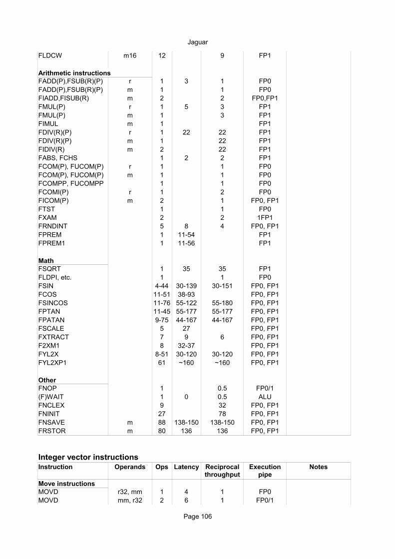
Jaguar
Page 106
FLDCW m16 12 9 FP1
Arithmetic instructionsFADD(P),FSUB(R)(P) r 1 3 1 FP0FADD(P),FSUB(R)(P) m 1 1 FP0FIADD,FISUB(R) m 2 2 FP0,FP1FMUL(P) r 1 5 3 FP1FMUL(P) m 1 3 FP1FIMUL m 1 FP1FDIV(R)(P) r 1 22 22 FP1FDIV(R)(P) m 1 22 FP1FIDIV(R) m 2 22 FP1FABS, FCHS 1 2 2 FP1FCOM(P), FUCOM(P) r 1 1 FP0FCOM(P), FUCOM(P) m 1 1 FP0FCOMPP, FUCOMPP 1 1 FP0FCOMI(P) r 1 2 FP0FICOM(P) m 2 1 FP0, FP1FTST 1 1 FP0FXAM 2 2 1FP1FRNDINT 5 8 4 FP0, FP1FPREM 1 11-54 FP1FPREM1 1 11-56 FP1
MathFSQRT 1 35 35 FP1FLDPI, etc. 1 1 FP0FSIN 4-44 30-139 30-151 FP0, FP1FCOS 11-51 38-93 FP0, FP1FSINCOS 11-76 55-122 55-180 FP0, FP1FPTAN 11-45 55-177 55-177 FP0, FP1FPATAN 9-75 44-167 44-167 FP0, FP1FSCALE 5 27 FP0, FP1FXTRACT 7 9 6 FP0, FP1F2XM1 8 32-37 FP0, FP1FYL2X 8-51 30-120 30-120 FP0, FP1FYL2XP1 61 ~160 ~160 FP0, FP1
OtherFNOP 1 0.5 FP0/1(F)WAIT 1 0 0.5 ALUFNCLEX 9 32 FP0, FP1FNINIT 27 78 FP0, FP1FNSAVE m 88 138-150 138-150 FP0, FP1FRSTOR m 80 136 136 FP0, FP1
Integer vector instructionsInstruction Operands Ops Latency Notes
Move instructionsMOVD r32, mm 1 4 1 FP0MOVD mm, r32 2 6 1 FP0/1
Reciprocal throughput
Execution pipe

Jaguar
Page 107
MOVD mm,m32 1 4 1 AGUMOVD r32, x 1 4 1 FP0MOVD x, r32 2 6 1 FP1MOVD x,m32 1 4 1 AGUMOVD m32,(x)mm 1 3 1 FP1
MOVD / MOVQ r64,(x)mm 1 4 1 FP0MOVQ mm,r64 2 6 1 FP0/1 do.MOVQ x,r64 2 6 1 FP0/1 do.MOVQ mm,mm 1 1 0.5 FP0/1MOVQ x,x 1 1 0.5 FP0/1MOVQ (x)mm,m64 1 4 1 AGUMOVQ m64,(x)mm 1 3 1 FP1MOVDQA x,x 1 1 0.5 FP0/1VMOVDQA y,y 2 1 1 FP0/1 AVXMOVDQA x,m 1 4 1 AGUVMOVDQA y,m 2 4 2 AGU AVXMOVDQA m,x 1 3 1 FP1VMOVDQA m,y 2 3 2 FP1 AVXMOVDQU, LDDQU x.m 1 4 1 AGUMOVDQU m,x 1 3 1 FP1MOVDQ2Q mm,x 1 1 0.5 FP0/1MOVQ2DQ x,mm 1 1 0.5 FP0/1MOVNTQ m,mm 1 429 2 FP1MOVNTDQ m,x 1 429 2 FP1
mm,r/m 1 1 0.5 FP0/1
x,r/m 1 2 0.5 FP0/1
mm,r/m 1 1 0.5 FP0/1
x,r/m 1 2 0.5 FP0/1PUNPCKH/LQDQ x,r/m 1 2 0.5 FP0/1PSHUFB mm,mm 1 1 0.5 FP0/1 Suppl. SSE3PSHUFB x,x 3 4 2 FP0/1 Suppl. SSE3PSHUFD x,x,i 1 2 0.5 FP0/1PSHUFW mm,mm,i 1 1 0.5 FP0/1PSHUFL/HW x,x,i 1 1 0.5 FP0/1PALIGNR x,x,i 1 2 0.5 FP0/1 Suppl. SSE3PBLENDW x,r/m 1 1 0.5 FP0/1 SSE4.1MASKMOVQ mm,mm 32 432 17 FP0, FP1MASKMOVDQU x,x 64 43-2210 34 FP0, FP1PMOVMSKB r32,(x)mm 1 3 1 FP0PEXTRW r32,(x)mm,i 1 4 1 FP0PINSRW mm,r32,i 2 8 1 FP0/1PINSRB/W/D/Q x,r,i 2 7 1 FP0/1PINSRB/W/D/Q x,m,i 1 1 FP0/1PEXTRB/W/D/Q r,x,i 1 3 1 FP0 SSE4.1PEXTRB/W/D/Q m,x,i 1 1 FP1 SSE4.1INSERTQ x,x 3 2 2 FP0, FP1 SSE4A, AMD onlyINSERTQ x,x,i,i 3 2 2 FP0, FP1 SSE4A, AMD onlyEXTRQ x,x 1 1 0.5 FP0/1 SSE4A, AMD only
Moves 64 bits.Name of instruction differs
PACKSSWB/DW PACKUSWB
PACKSSWB/DW PACKUSWB
PUNPCKH/LBW/WD/DQ
PUNPCKH/LBW/WD/DQ

Jaguar
Page 108
EXTRQ x,x,i,i 1 1 0.5 FP0/1 SSE4A, AMD only
x,x 1 2 0.5 FP0/1 SSE4.1
x,x 1 2 0.5 FP0/1 SSE4.1
Arithmetic instructions
(x)mm,r/m 1 1 0.5 FP0/1PHADD/SUBW/SW/D mm,r/m 1 1 0.5 FP0/1 Suppl. SSE3PHADD/SUBW/SW/D x,r/m 1 2 0.5 FP0/1 Suppl. SSE3PCMPEQ/GT B/W/D mm,r/m 1 1 0.5 FP0/1PCMPEQ/GT B/W/D x,r/m 1 1 0.5 FP0/1PCMPEQQ (x)mm,r/m 1 1 0.5 FP0/1 SSE4.1PCMPGTQ (x)mm,r/m 1 1 0.5 FP0/1 SSE4.2
(x)mm,r/m 1 2 1 FP0PMULLD x,r/m 3 4 2 FP0 FP1 SSE4.1PMULDQ x,r/m 1 2 1 FP0 SSE4.1PMULHRSW (x)mm,r/m 1 2 1 FP0 Suppl. SSE3PMADDWD (x)mm,r/m 1 2 1 FP0PMADDUBSW (x)mm,r/m 1 2 1 FP0 Suppl. SSE3PAVGB/W (x)mm,r/m 1 1 0.5 FP0/1PMIN/MAX SW/UB (x)mm,r/m 1 1 0.5 FP0/1PABSB/W/D (x)mm,r/m 1 1 0.5 FP0/1 Suppl. SSE3PSIGNB/W/D (x)mm,r/m 1 1 0.5 FP0/1 Suppl. SSE3PSADBW (x)mm,r/m 1 2 0.5 FP0/1MPSADBW x,x,i 3 4 1 FP0/1 SSE4.1
Logic
(x)mm,r/m 1 1 0.5 FP0/1
mm,i/mm/m 1 1 0.5 FP0/1
x,x 1 2 0.5 FP0/1
x,i 1 1 0.5 FP0/1PSLLDQ, PSRLDQ x,i 1 2 0.5 FP0/1PTEST x,x/m 1 3 1 FP0 SSE4.1
String instructionsPCMPESTRI x,x,i 9 5 5 FP0/1 SSE4.2PCMPESTRI x,m,i 10 5 FP0/1 SSE4.2PCMPESTRM x,x,i 9 9 9 FP0/1 SSE4.2PCMPESTRM x,m,i 10 9 FP0/1 SSE4.2PCMPISTRI x,x,i 3 2 2 FP0/1 SSE4.2PCMPISTRI x,m,i 4 2 FP0/1 SSE4.2
PMOVSXBW/BD/BQ/WD/WQ/DQ
PMOVZXBW/BD/BQ/WD/WQ/DQ
PADDB/W/D/Q PADDSB/W ADDUSB/W PSUBB/W/D/Q PSUBSB/W PSUBUSB/W
PMULLW PMULHW PMULHUW PMULUDQ
PAND PANDN POR PXOR
PSLL/RL W/D/Q PSRAW/D
PSLL/RL W/D/Q PSRAW/D
PSLL/RL W/D/Q PSRAW/D

Jaguar
Page 109
PCMPISTRM x,x,i 3 8 8 FP0/1 SSE4.2PCMPISTRM x,m,i 4 2 FP0/1 SSE4.2
EncryptionPCLMULQDQ x,x/m,i 1 3 1 FP0 PCLMULAESDEC x,x 2 5 1 FP0/1 AESAESDECLAST x,x 2 5 1 FP0/1 AESAESENC x,x 2 5 1 FP0/1 AESAESENCLAST x,x 2 5 1 FP0/1 AESAESIMC x,x 1 2 1 FP0/1 AESAESKEYGENASSIST x,x,i 1 2 1 FP0/1 AES
OtherEMMS 1 0.5 FP0/1
Floating point XMM instructionsInstruction Operands Ops Latency Notes
Move instructionsMOVAPS/D x,x 1 1 0.5 FP0/1VMOVAPS/D y,y 2 1 1 FP0/1MOVAPS/D x,m 1 4 1 AGUVMOVAPS/D y,m 2 4 2 AGUMOVAPS/D m,x 1 3 1 FP1VMOVAPS/D m,y 2 3 2 FP1MOVUPS/D x,x 1 1 0.5 FP0/1VMOVUPS/D y,y 2 1 1 FP0/1MOVUPS/D x,m 1 4 1 AGUVMOVUPS/D y,m 2 4 2 AGUMOVUPS/D m,x 1 3 1 FP1VMOVUPS/D m,y 2 3 2 FP1MOVSS/D x,x 1 1 0.5 FP0/1MOVSS/D x,m 1 4 1 AGUMOVSS/D m,x 1 3 1 FP1MOVHLPS, MOVLHPS
x,x 1 2 2 FP0/1
x,m 1 5 1 FP0/1
m,x 1 4 1 FP1MOVNTPS/D m,x 1 429 1 FP1MOVNTSS/D m,x 1 1 FP1 SSE4A, AMD onlyMOVDDUP x,x 1 2 0.5 FP0/1 SSE3MOVDDUP x,m64 1 1 AGU SSE3VMOVDDUP y,y 2 2 1 FP0/1 AVXVMOVDDUP y,m 2 2 AGU AVXMOVSH/LDUP x,x 1 1 0.5 FP0/1MOVSH/LDUP x,m 1 1 AGUVMOVSH/LDUP y,y 2 1 1 FP0/1 AVXVMOVSH/LDUP y,m 2 2 AGU AVXMOVMSKPS/D r32,x 1 3 1 FP0VMOVMSKPS/D r32,y 1 3 1 FP0 AVX
Reciprocal throughput
Execution pipe
MOVHPS/D, MOVLPS/D
MOVHPS/D, MOVLPS/D

Jaguar
Page 110
SHUFPS/D x,x/m,i 1 2 0.5 FP0/1VSHUFPS/D y,y,y,i 2 2 1 FP0/1 AVXUNPCK H/L PS/D x,x/m 1 2 0.5 FP0/1VUNPCK H/L PS/D y,y,y 2 2 1 FP0/1 AVXEXTRACTPS r32,x,i 1 3 1 FP0EXTRACTPS m32,x,i 1 3 1 FP1VEXTRACTF128 x,y,i 1 1 0.5 FP0/1 AVXVEXTRACTF128 m128,y,i 1 12 1 FP1 AVXINSERTPS x,x,i 1 1 FP0/1INSERTPS x,m32,i 1 6 1 FP0/1VINSERTF128 y,y,x,i 2 1 1 FP0/1 AVXVINSERTF128 y,y,m128,i 2 13 2 FP0/1 AVXVMASKMOVPS/D x,x,m128 1 15 1 FP0/1 >300 clk if mask=0VMASKMOVPS/D y,y,m256 2 15 2 FP0/1 >300 clk if mask=0VMASKMOVPS/D m128,x,x 19 21 16 FP1 AVXVMASKMOVPS/D m256,y,y 36 32 22 FP1 AVX
ConversionCVTPS2PD x,x/m 1 3 1 FP1VCVTPS2PD y,x/m 2 4 2 FP1CVTPD2PS x,x/m 1 4 1 FP1VCVTPD2PS x,y 3 6 2 FP0, FP1CVTSD2SS x,x/m 2 5 8 FP1CVTSS2SD x,x/m 2 4 7 FP1CVTDQ2PS/PD x,x/m 1 4 1 FP1VCVTDQ2PS/PD y,y 2 4 2 FP1CVT(T)PS2DQ x,x/m 1 4 1 FP1VCVT(T)PS2DQ y,y 2 4 2 FP1CVT(T)PD2DQ x,x/m 1 4 1 FP1VCVT(T)PD2DQ y,y 3 7 2 FP1CVTPI2PS xmm,mm 1 4 1 FP1CVTPI2PD xmm,mm 1 4 1 FP1CVT(T)PS2PI mm,xmm 1 4 1 FP1CVT(T)PD2PI mm,xmm 1 4 1 FP1CVTSI2SS xmm,r32 2 9 1 FP1CVTSI2SD xmm,r32 2 9 1 FP1CVT(T)SS2SI r32,xmm 2 8 1 FP1CVT(T)SD2SI r32,xmm 2 8 1 FP1VCVTPS2PH x/m,x,i 1 4 1 FP1 F16CVCVTPS2PH x/m,y,i 3 6 2 FP0, FP1 F16CVCVTPH2PS x,x/m 1 4 1 FP1 F16CVCVTPH2PS y,x/m 2 5 2 FP1 F16C
ArithmeticADDSS/D SUBSS/D x,x/m 1 3 1 FP0ADDPS/D SUBPS/D x,x/m 1 3 1 FP0VADDPS/D VSUBPS/D y,y/m 2 3 2 FP0ADDSUBPS/D x,x/m 1 3 1 FP0 SSE3VADDSUBPS/D y,y/m 2 3 2 FP0HADD/SUBPS/D x,x/m 1 4 1 FP0 SSE3VHADD/SUBPS/D y,y/m 2 4 2 FP0MULSS/PS x,x/m 1 2 1 FP1VMULPS y,y/m 2 2 2 FP1

Jaguar
Page 111
MULSD/PD x,x/m 1 4 2 FP1VMULPD y,y/m 2 4 2 FP1DIVSS x,x/m 1 14 14 FP1DIVPS x,x/m 1 19 19 FP1VDIVPS y,y/m 2 38 38 FP1DIVSD x,x/m 1 19 19 FP1DIVPD x,x/m 1 19 19 FP1VDIVPD y,y/m 2 38 38 FP1RCPSS x,x/m 1 2 1 FP1RCPPS x,x/m 1 2 1 FP1VRCPPS y,y/m 2 2 2 FP1MAXSS/D MINSS/D x,x/m 1 2 1 FP0MAXPS/D MINPS/D x,x/m 1 2 1 FP0VMAXPS/D VMINPS/D y,y/m 2 2 2 FP0CMPccSS/D x,x/m 1 2 1 FP0CMPccPS/D x,x/m 1 2 1 FP0VCMPccPS/D y,y/m 2 2 2 FP0(U)COMISS/D x,x/m 1 1 FP0ROUNDSS/SD/PS/PD x,x/m,i 1 4 1 FP1VROUNDSS/D/PS/D y,y/m,i 2 4 2 FP1DPPS x,x,i 5 11 4 FP0, FP1 SSE4.1DPPS x,m,i 6 4 FP0, FP1 SSE4.1VDPPS y,y,y,i 10 12 7 FP0, FP1 SSE4.1VDPPS y,m,i 12 7 FP0, FP1 SSE4.1DPPD x,x,i 3 9 3 FP0, FP1 SSE4.1DPPD x,m,i 4 3 FP0, FP1 SSE4.1
Logic
x,x/m 1 1 0.5 FP0/1VANDPS/D, etc. y,y/m 2 1 1 FP0/1
MathSQRTSS x,x/m 1 16 16 FP1SQRTPS x,x/m 2 21 21 FP1VSQRTPS y,y/m 2 42 42 FP1SQRTSD x,x/m 1 27 27 FP1SQRTPD x,x/m 2 27 27 FP1VSQRTPD y,y/m 2 54 54 FP1RSQRTSS/PS x,x/m 1 2 1 FP1VRSQRTPS y,y/m 2 2 2 FP1
OtherLDMXCSR m 12 9 8 FP0, FP1STMXCSR m 3 13 12 FP0, FP1VZEROUPPER 21 30 32 bit modeVZEROUPPER 37 46 64 bit modeVZEROALL 41 58 32 bit modeVZEROALL 73 90 64 bit modeFXSAVE 66 66 66 32 bit modeFXSAVE 58 58 58 64 bit modeFXRSTOR 115 189 189 32 bit modeFXRSTOR 123 198 197 64 bit mode
ANDPS/D ANDNPS/D ORPS/D XORPS/D

Jaguar
Page 112
XSAVE 130 145 145 32 bit modeXSAVE 114 129 129 64 bit modeXRSTOR 219 342 342 32 bit modeXRSTOR 251 375 375 64 bit mode
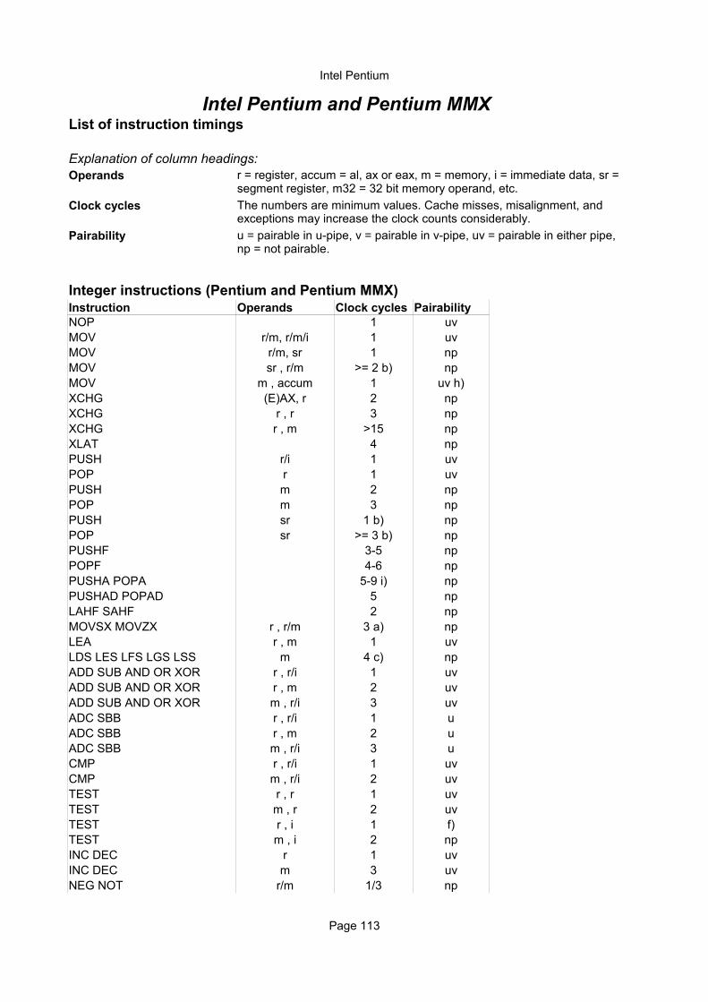
Intel Pentium
Page 113
Intel Pentium and Pentium MMXList of instruction timings
Explanation of column headings:Operands
Clock cycles
Pairability
Integer instructions (Pentium and Pentium MMX) Instruction Operands Clock cycles PairabilityNOP 1 uvMOV r/m, r/m/i 1 uvMOV r/m, sr 1 npMOV sr , r/m >= 2 b) npMOV m , accum 1 uv h)XCHG (E)AX, r 2 npXCHG r , r 3 npXCHG r , m >15 npXLAT 4 npPUSH r/i 1 uvPOP r 1 uvPUSH m 2 npPOP m 3 npPUSH sr 1 b) npPOP sr >= 3 b) npPUSHF 3-5 npPOPF 4-6 npPUSHA POPA 5-9 i) npPUSHAD POPAD 5 npLAHF SAHF 2 npMOVSX MOVZX r , r/m 3 a) npLEA r , m 1 uvLDS LES LFS LGS LSS m 4 c) npADD SUB AND OR XOR r , r/i 1 uvADD SUB AND OR XOR r , m 2 uvADD SUB AND OR XOR m , r/i 3 uvADC SBB r , r/i 1 uADC SBB r , m 2 uADC SBB m , r/i 3 uCMP r , r/i 1 uvCMP m , r/i 2 uvTEST r , r 1 uvTEST m , r 2 uvTEST r , i 1 f)TEST m , i 2 npINC DEC r 1 uvINC DEC m 3 uvNEG NOT r/m 1/3 np
r = register, accum = al, ax or eax, m = memory, i = immediate data, sr = segment register, m32 = 32 bit memory operand, etc.
The numbers are minimum values. Cache misses, misalignment, and exceptions may increase the clock counts considerably.
u = pairable in u-pipe, v = pairable in v-pipe, uv = pairable in either pipe, np = not pairable.
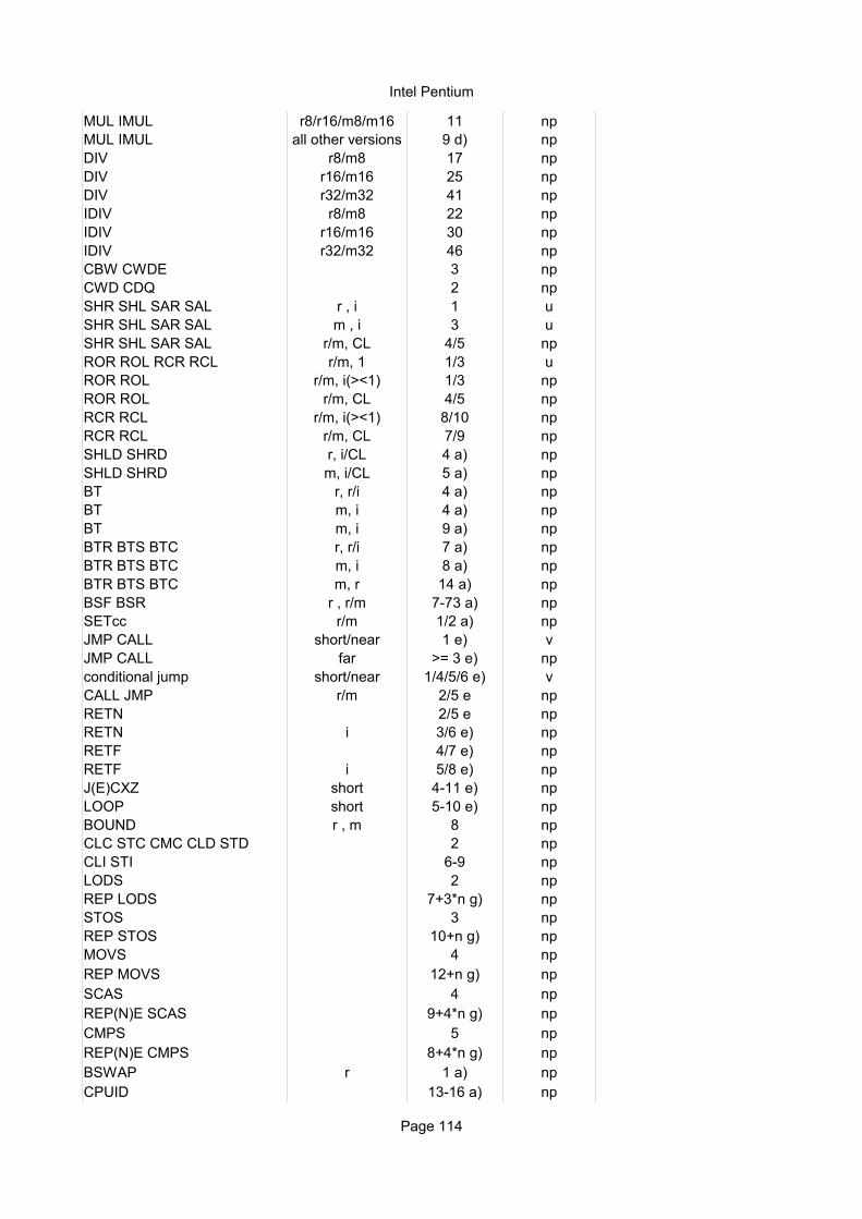
Intel Pentium
Page 114
MUL IMUL r8/r16/m8/m16 11 npMUL IMUL all other versions 9 d) npDIV r8/m8 17 npDIV r16/m16 25 npDIV r32/m32 41 npIDIV r8/m8 22 npIDIV r16/m16 30 npIDIV r32/m32 46 npCBW CWDE 3 npCWD CDQ 2 npSHR SHL SAR SAL r , i 1 uSHR SHL SAR SAL m , i 3 uSHR SHL SAR SAL r/m, CL 4/5 npROR ROL RCR RCL r/m, 1 1/3 uROR ROL r/m, i(><1) 1/3 npROR ROL r/m, CL 4/5 npRCR RCL r/m, i(><1) 8/10 npRCR RCL r/m, CL 7/9 npSHLD SHRD r, i/CL 4 a) npSHLD SHRD m, i/CL 5 a) npBT r, r/i 4 a) npBT m, i 4 a) npBT m, i 9 a) npBTR BTS BTC r, r/i 7 a) npBTR BTS BTC m, i 8 a) npBTR BTS BTC m, r 14 a) npBSF BSR r , r/m 7-73 a) npSETcc r/m 1/2 a) npJMP CALL short/near 1 e) vJMP CALL far >= 3 e) npconditional jump short/near 1/4/5/6 e) vCALL JMP r/m 2/5 e npRETN 2/5 e npRETN i 3/6 e) npRETF 4/7 e) npRETF i 5/8 e) npJ(E)CXZ short 4-11 e) npLOOP short 5-10 e) npBOUND r , m 8 npCLC STC CMC CLD STD 2 npCLI STI 6-9 npLODS 2 npREP LODS 7+3*n g) npSTOS 3 npREP STOS 10+n g) npMOVS 4 npREP MOVS 12+n g) npSCAS 4 npREP(N)E SCAS 9+4*n g) npCMPS 5 npREP(N)E CMPS 8+4*n g) npBSWAP r 1 a) npCPUID 13-16 a) np
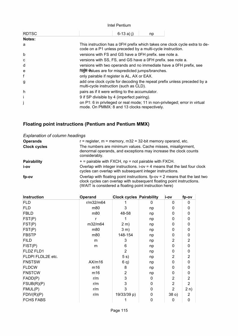
Intel Pentium
Page 115
RDTSC 6-13 a) j) npNotes:a
b versions with FS and GS have a 0FH prefix. see note a.c versions with SS, FS, and GS have a 0FH prefix. see note a.de high values are for mispredicted jumps/branches.f only pairable if register is AL, AX or EAX.g
h pairs as if it were writing to the accumulator.i 9 if SP divisible by 4 (imperfect pairing).j
Floating point instructions (Pentium and Pentium MMX)
Explanation of column headingsOperands r = register, m = memory, m32 = 32-bit memory operand, etc.Clock cycles
Pairability + = pairable with FXCH, np = not pairable with FXCH.i-ov
fp-ov
Instruction Operand Clock cycles Pairability i-ov fp-ovFLD r/m32/m64 1 0 0 0FLD m80 3 np 0 0FBLD m80 48-58 np 0 0FST(P) r 1 np 0 0FST(P) m32/m64 2 m) np 0 0FST(P) m80 3 m) np 0 0FBSTP m80 148-154 np 0 0FILD m 3 np 2 2FIST(P) m 6 np 0 0FLDZ FLD1 2 np 0 0FLDPI FLDL2E etc. 5 s) np 2 2FNSTSW AX/m16 6 q) np 0 0FLDCW m16 8 np 0 0FNSTCW m16 2 np 0 0FADD(P) r/m 3 0 2 2FSUB(R)(P) r/m 3 0 2 2FMUL(P) r/m 3 0 2 2 n)FDIV(R)(P) r/m 19/33/39 p) 0 38 o) 2FCHS FABS 1 0 0 0
This instruction has a 0FH prefix which takes one clock cycle extra to de-code on a P1 unless preceded by a multi-cycle instruction.
versions with two operands and no immediate have a 0FH prefix, see note a.
add one clock cycle for decoding the repeat prefix unless preceded by a multi-cycle instruction (such as CLD).
on P1: 6 in privileged or real mode; 11 in non-privileged; error in virtual mode. On PMMX: 8 and 13 clocks respectively.
The numbers are minimum values. Cache misses, misalignment, denormal operands, and exceptions may increase the clock counts considerably.
Overlap with integer instructions. i-ov = 4 means that the last four clock cycles can overlap with subsequent integer instructions.
Overlap with floating point instructions. fp-ov = 2 means that the last two clock cycles can overlap with subsequent floating point instructions. (WAIT is considered a floating point instruction here)

Intel Pentium
Page 116
FCOM(P)(P) FUCOM r/m 1 0 0 0FIADD FISUB(R) m 6 np 2 2FIMUL m 6 np 2 2FIDIV(R) m 22/36/42 p) np 38 o) 2FICOM m 4 np 0 0FTST 1 np 0 0FXAM 17-21 np 4 0FPREM 16-64 np 2 2FPREM1 20-70 np 2 2FRNDINT 9-20 np 0 0FSCALE 20-32 np 5 0FXTRACT 12-66 np 0 0FSQRT 70 np 69 o) 2FSIN FCOS 65-100 r) np 2 2FSINCOS 89-112 r) np 2 2F2XM1 53-59 r) np 2 2FYL2X 103 r) np 2 2FYL2XP1 105 r) np 2 2FPTAN 120-147 r) np 36 o) 0FPATAN 112-134 r) np 2 2FNOP 1 np 0 0FXCH r 1 np 0 0FINCSTP FDECSTP 2 np 0 0FFREE r 2 np 0 0FNCLEX 6-9 np 0 0FNINIT 12-22 np 0 0FNSAVE m 124-300 np 0 0FRSTOR m 70-95 np 0 0WAIT 1 np 0 0Notes:m The value to store is needed one clock cycle in advance.n 1 if the overlapping instruction is also an FMUL.o Cannot overlap integer multiplication instructions.p
q The first 4 clock cycles can overlap with preceding integer instructions.r
s
MMX instructions (Pentium MMX)
FDIV takes 19, 33, or 39 clock cycles for 24, 53, and 64 bit precision re-spectively. FIDIV takes 3 clocks more. The precision is defined by bit 8-9 of the floating point control word.
Clock counts are typical. Trivial cases may be faster, extreme cases may be slower.
May be up to 3 clocks more when output needed for FST, FCHS, or FABS.
A list of MMX instruction timings is not needed because they all take one clock cycle, except the MMX multiply instructions which take 3. MMX multiply instructions can be pipelined to yield a throughput of one multiplication per clock cycle.
The EMMS instruction takes only one clock cycle, but the first floating point instruction after an EMMS takes approximately 58 clocks extra, and the first MMX instruction after a floating point instruction takes approximately 38 clocks extra. There is no penalty for an MMX instruction after EMMS on the PMMX.

Intel Pentium
Page 117
There is no penalty for using a memory operand in an MMX instruction because the MMX arithmetic unit is one step later in the pipeline than the load unit. But the penalty comes when you store data from an MMX register to memory or to a 32-bit register: The data have to be ready one clock cycle in advance. This is analogous to the floating point store instructions.
All MMX instructions except EMMS are pairable in either pipe. Pairing rules for MMX instructions are de-scribed in manual 3: "The microarchitecture of Intel, AMD and VIA CPUs".

Pentium II and III
Page 118
Intel Pentium II and Pentium IIIList of instruction timings and μop breakdown
Explanation of column headings:Operands:
μops: The number of μops that the instruction generates for each execution port.p0: Port 0: ALU, etc.p1: Port 1: ALU, jumpsp01: Instructions that can go to either port 0 or 1, whichever is vacant first.p2: Port 2: load data, etc.p3: Port 3: address generation for storep4: Port 4: store dataLatency:
Reciprocal throughput:
Integer instructions (Pentium Pro, Pentium II and Pentium III) Instruction Operands μops Latency
p0 p1 p01 p2 p3 p4MOV r,r/i 1MOV r,m 1MOV m,r/i 1 1MOV r,sr 1MOV m,sr 1 1 1MOV sr,r 8 5MOV sr,m 7 1 8MOVSX MOVZX r,r 1MOVSX MOVZX r,m 1CMOVcc r,r 1 1CMOVcc r,m 1 1 1XCHG r,r 3XCHG r,m 4 1 1 1 high b)XLAT 1 1PUSH r/i 1 1 1POP r 1 1POP (E)SP 2 1PUSH m 1 1 1 1POP m 5 1 1 1PUSH sr 2 1 1POP sr 8 1
i = immediate data, r = register, mm = 64 bit mmx register, xmm = 128 bit xmm register, sr = segment register, m = memory, m32 = 32-bit memory operand, etc.
This is the delay that the instruction generates in a dependency chain. (This is not the same as the time spent in the execution unit. Values may be inaccurate in situations where they cannot be measured exactly, especially with memory operands). The numbers are minimum values. Cache misses, misalignment, and exceptions may increase the clock counts considerably. Floating point operands are presumed to be normal numbers. Denormal numbers, NAN's and infinity in-crease the delays by 50-150 clocks, except in XMM move, shuffle and Boolean instructions. Floating point overflow, underflow, denormal or NAN results give a similar delay.
The average number of clock cycles per instruction for a series of independent instructions of the same kind.
Reciprocal throughput
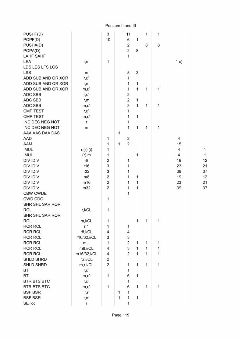
Pentium II and III
Page 119
PUSHF(D) 3 11 1 1POPF(D) 10 6 1PUSHA(D) 2 8 8POPA(D) 2 8LAHF SAHF 1LEA r,m 1 1 c)LDS LES LFS LGSLSS m 8 3ADD SUB AND OR XOR r,r/i 1ADD SUB AND OR XOR r,m 1 1ADD SUB AND OR XOR m,r/i 1 1 1 1ADC SBB r,r/i 2ADC SBB r,m 2 1ADC SBB m,r/i 3 1 1 1CMP TEST r,r/i 1CMP TEST m,r/i 1 1INC DEC NEG NOT r 1INC DEC NEG NOT m 1 1 1 1AAA AAS DAA DAS 1AAD 1 2 4AAM 1 1 2 15IMUL r,(r),(i) 1 4 1IMUL (r),m 1 1 4 1DIV IDIV r8 2 1 19 12DIV IDIV r16 3 1 23 21DIV IDIV r32 3 1 39 37DIV IDIV m8 2 1 1 19 12DIV IDIV m16 2 1 1 23 21DIV IDIV m32 2 1 1 39 37CBW CWDE 1CWD CDQ 1SHR SHL SAR RORROL r,i/CL 1SHR SHL SAR RORROL m,i/CL 1 1 1 1RCR RCL r,1 1 1RCR RCL r8,i/CL 4 4RCR RCL r16/32,i/CL 3 3RCR RCL m,1 1 2 1 1 1RCR RCL m8,i/CL 4 3 1 1 1RCR RCL m16/32,i/CL 4 2 1 1 1SHLD SHRD r,r,i/CL 2SHLD SHRD m,r,i/CL 2 1 1 1 1BT r,r/i 1BT m,r/i 1 6 1BTR BTS BTC r,r/i 1BTR BTS BTC m,r/i 1 6 1 1 1BSF BSR r,r 1 1BSF BSR r,m 1 1 1SETcc r 1

Pentium II and III
Page 120
SETcc m 1 1 1JMP short/near 1 2JMP far 21 1JMP r 1 2JMP m(near) 1 1 2JMP m(far) 21 2conditional jump short/near 1 2CALL near 1 1 1 1 2CALL far 28 1 2 2CALL r 1 2 1 1 2CALL m(near) 1 4 1 1 1 2CALL m(far) 28 2 2 2RETN 1 2 1 2RETN i 1 3 1 2RETF 23 3RETF i 23 3J(E)CXZ short 1 1LOOP short 2 1 8LOOP(N)E short 2 1 8ENTER i,0 12 1 1ENTER a,b ca. 18 +4b b-1 2bLEAVE 2 1BOUND r,m 7 6 2CLC STC CMC 1CLD STD 4CLI 9STI 17INTO 5LODS 2REP LODS 10+6nSTOS 1 1 1REP STOS ca. 5n a)MOVS 1 3 1 1REP MOVS ca. 6n a)SCAS 1 2REP(N)E SCAS 12+7nCMPS 4 2REP(N)E CMPS 12+9nBSWAP r 1 1NOP (90) 1 0,5Long NOP (0F 1F) 1 1CPUID 23-48RDTSC 31IN 18 >300OUT 18 >300PREFETCHNTA d) m 1PREFETCHT0/1/2 d) m 1SFENCE d) 1 1 6Notes
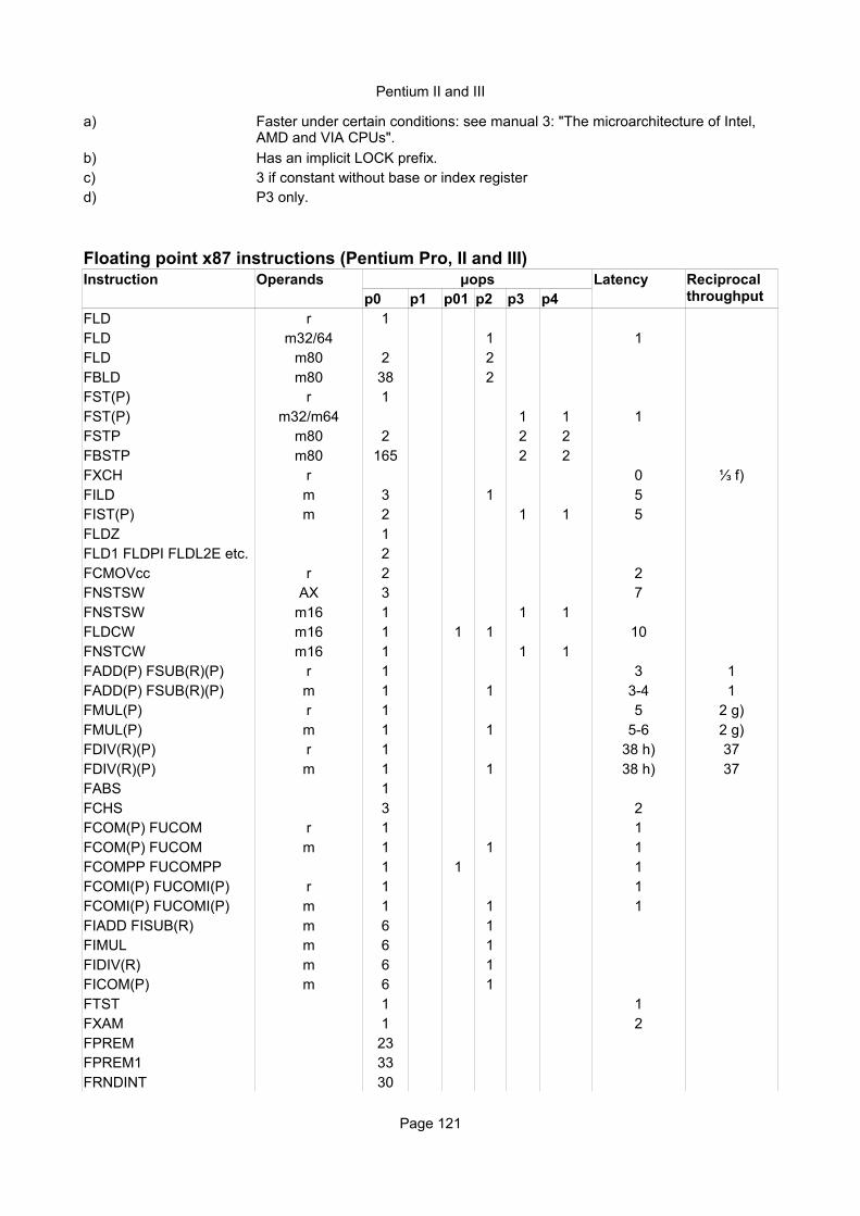
Pentium II and III
Page 121
a)
b) Has an implicit LOCK prefix. c) 3 if constant without base or index registerd) P3 only.
Floating point x87 instructions (Pentium Pro, II and III)Instruction Operands μops Latency
p0 p1 p01 p2 p3 p4FLD r 1FLD m32/64 1 1FLD m80 2 2FBLD m80 38 2FST(P) r 1FST(P) m32/m64 1 1 1FSTP m80 2 2 2FBSTP m80 165 2 2FXCH r 0 ⅓ f)FILD m 3 1 5FIST(P) m 2 1 1 5FLDZ 1FLD1 FLDPI FLDL2E etc. 2FCMOVcc r 2 2FNSTSW AX 3 7FNSTSW m16 1 1 1FLDCW m16 1 1 1 10FNSTCW m16 1 1 1FADD(P) FSUB(R)(P) r 1 3 1FADD(P) FSUB(R)(P) m 1 1 3-4 1FMUL(P) r 1 5 2 g)FMUL(P) m 1 1 5-6 2 g)FDIV(R)(P) r 1 38 h) 37FDIV(R)(P) m 1 1 38 h) 37FABS 1FCHS 3 2FCOM(P) FUCOM r 1 1FCOM(P) FUCOM m 1 1 1FCOMPP FUCOMPP 1 1 1FCOMI(P) FUCOMI(P) r 1 1FCOMI(P) FUCOMI(P) m 1 1 1FIADD FISUB(R) m 6 1FIMUL m 6 1FIDIV(R) m 6 1FICOM(P) m 6 1FTST 1 1FXAM 1 2FPREM 23FPREM1 33FRNDINT 30
Faster under certain conditions: see manual 3: "The microarchitecture of Intel, AMD and VIA CPUs".
Reciprocal throughput

Pentium II and III
Page 122
FSCALE 56FXTRACT 15FSQRT 1 69 e,i)FSIN FCOS 17-97 27-103 e)FSINCOS 18-110 29-130 e)F2XM1 17-48 66 e)FYL2X 36-54 103 e)FYL2XP1 31-53 98-107 e)FPTAN 21-102 13-143 e)FPATAN 25-86 44-143 e)FNOP 1FINCSTP FDECSTP 1FFREE r 1FFREEP r 2FNCLEX 3FNINIT 13FNSAVE 141FRSTOR 72WAIT 2Notes:e) Not pipelinedf)
g)
h)
i) Faster for lower precision.
Integer MMX instructions (Pentium II and Pentium III)Instruction Operands μops Latency
p0 p1 p01 p2 p3 p4MOVD MOVQ r,r 1 1 0,5MOVD MOVQ mm,m32/64 1 1MOVD MOVQ m32/64,mm 1 1 1PADD PSUB PCMP mm,mm 1 1 0,5PADD PSUB PCMP mm,m64 1 1 1PMUL PMADD mm,mm 1 3 1PMUL PMADD mm,m64 1 1 3 1PAND(N) POR PXOR mm,mm 1 1 0,5PAND(N) POR PXOR mm,m64 1 1 1PSRA PSRL PSLL mm,mm/i 1 1 1PSRA PSRL PSLL mm,m64 1 1 1PACK PUNPCK mm,mm 1 1 1PACK PUNPCK mm,m64 1 1 1EMMS 11 6 k)MASKMOVQ d) mm,mm 1 1 1 2-8 2 - 30
FXCH generates 1 μop that is resolved by register renaming without going to any port.
FMUL uses the same circuitry as integer multiplication. Therefore, the combined throughput of mixed floating point and integer multiplications is 1 FMUL + 1 IMUL per 3 clock cycles.
FDIV latency depends on precision specified in control word: 64 bits precision gives latency 38, 53 bits precision gives latency 32, 24 bits precision gives la-tency 18. Division by a power of 2 takes 9 clocks. Reciprocal throughput is 1/(la-tency-1).
Reciprocal throughput

Pentium II and III
Page 123
PMOVMSKB d) r32,mm 1 1 1MOVNTQ d) m64,mm 1 1 1 - 30PSHUFW d) mm,mm,i 1 1 1PSHUFW d) mm,m64,i 1 1 2 1PEXTRW d) r32,mm,i 1 1 2 1PINSRW d) mm,r32,i 1 1 1PINSRW d) mm,m16,i 1 1 2 1PAVGB PAVGW d) mm,mm 1 1 0,5PAVGB PAVGW d) mm,m64 1 1 2 1PMIN/MAXUB/SW d) mm,mm 1 1 0,5PMIN/MAXUB/SW d) mm,m64 1 1 2 1PMULHUW d) mm,mm 1 3 1PMULHUW d) mm,m64 1 1 4 1PSADBW d) mm,mm 2 1 5 2PSADBW d) mm,m64 2 1 1 6 2Notes:d) P3 only.k)
Floating point XMM instructions (Pentium III)Instruction Operands μops Latency
p0 p1 p01 p2 p3 p4MOVAPS xmm,xmm 2 1 1MOVAPS xmm,m128 2 2 2MOVAPS m128,xmm 2 2 3 2MOVUPS xmm,m128 4 2 4MOVUPS m128,xmm 1 4 4 3 4MOVSS xmm,xmm 1 1 1MOVSS xmm,m32 1 1 1 1MOVSS m32,xmm 1 1 1 1MOVHPS MOVLPS xmm,m64 1 1 1MOVHPS MOVLPS m64,xmm 1 1 1 1MOVLHPS MOVHLPS xmm,xmm 1 1 1MOVMSKPS r32,xmm 1 1 1MOVNTPS m128,xmm 2 2 2 - 15CVTPI2PS xmm,mm 2 3 1CVTPI2PS xmm,m64 2 1 4 2CVT(T)PS2PI mm,xmm 2 3 1CVTPS2PI mm,m128 1 2 4 1CVTSI2SS xmm,r32 2 1 4 2CVTSI2SS xmm,m32 2 2 5 2CVT(T)SS2SI r32,xmm 1 1 3 1CVTSS2SI r32,m128 1 2 4 2ADDPS SUBPS xmm,xmm 2 3 2ADDPS SUBPS xmm,m128 2 2 3 2ADDSS SUBSS xmm,xmm 1 3 1ADDSS SUBSS xmm,m32 1 1 3 1
The delay can be hidden by inserting other instructions between EMMS and any subsequent floating point instruction.
Reciprocal throughput

Pentium II and III
Page 124
MULPS xmm,xmm 2 4 2MULPS xmm,m128 2 2 4 2MULSS xmm,xmm 1 4 1MULSS xmm,m32 1 1 4 1DIVPS xmm,xmm 2 48 34DIVPS xmm,m128 2 2 48 34DIVSS xmm,xmm 1 18 17DIVSS xmm,m32 1 1 18 17AND(N)PS ORPS XORPS xmm,xmm 2 2 2AND(N)PS ORPS XORPS xmm,m128 2 2 2 2MAXPS MINPS xmm,xmm 2 3 2MAXPS MINPS xmm,m128 2 2 3 2MAXSS MINSS xmm,xmm 1 3 1MAXSS MINSS xmm,m32 1 1 3 1CMPccPS xmm,xmm 2 3 2CMPccPS xmm,m128 2 2 3 2CMPccSS xmm,xmm 1 3 1CMPccSS xmm,m32 1 1 3 1COMISS UCOMISS xmm,xmm 1 1 1COMISS UCOMISS xmm,m32 1 1 1 1SQRTPS xmm,xmm 2 56 56SQRTPS xmm,m128 2 2 57 56SQRTSS xmm,xmm 2 30 28SQRTSS xmm,m32 2 1 31 28RSQRTPS xmm,xmm 2 2 2RSQRTPS xmm,m128 2 2 3 2RSQRTSS xmm,xmm 1 1 1RSQRTSS xmm,m32 1 1 2 1RCPPS xmm,xmm 2 2 2RCPPS xmm,m128 2 2 3 2RCPSS xmm,xmm 1 1 1RCPSS xmm,m32 1 1 2 1SHUFPS xmm,xmm,i 2 1 2 2SHUFPS xmm,m128,i 2 2 2 2UNPCKHPS UNPCKLPS xmm,xmm 2 2 3 2UNPCKHPS UNPCKLPS xmm,m128 2 2 3 2LDMXCSR m32 11 15 15STMXCSR m32 6 7 9FXSAVE m4096 116 62FXRSTOR m4096 89 68

Pentium M
Page 125
Intel Pentium M, Core Solo and Core DuoList of instruction timings and μop breakdown
Explanation of column headings:Operands:
μops fused domain:
μops unfused domain:
p0: Port 0: ALU, etc.p1: Port 1: ALU, jumpsp01:
p2: Port 2: load data, etc.p3: Port 3: address generation for storep4: Port 4: store dataLatency:
Reciprocal throughput:
Integer instructionsInstruction Operands μops unfused domain Latency
p0 p1 p01 p2 p3 p4
Move instructions
MOV r,r/i 1 1 0,5MOV r,m 1 1 1MOV m,r 1 1 1 1MOV m,i 2 1 1 1MOV r,sr 1 1MOV m,sr 2 1 1 1MOV sr,r 8 8 5MOV sr,m 8 7 1 8MOVNTI m,r32 2 1 1 2MOVSX MOVZX r,r 1 1 1 0,5MOVSX MOVZX r,m 1 1 1CMOVcc r,r 2 1 1 2 1,5CMOVcc r,m 2 1 1 1XCHG r,r 3 3 2 1,5
i = immediate data, r = register, mm = 64 bit mmx register, xmm = 128 bit xmm register, sr = segment register, m = memory, m32 = 32-bit memory operand, etc.
The number of μops at the decode, rename, allocate and retire-ment stages in the pipeline. Fused μops count as one.
The number of μops for each execution port. Fused μops count as two.
Instructions that can go to either port 0 or 1, whichever is vacant first.
This is the delay that the instruction generates in a dependency chain. (This is not the same as the time spent in the execution unit. Values may be inaccurate in situations where they cannot be measured exactly, especially with memory operands). The num-bers are minimum values. Cache misses, misalignment, and ex-ceptions may increase the clock counts considerably. Floating point operands are presumed to be normal numbers. Denormal numbers, NAN's and infinity increase the delays by 50-150 clocks, except in XMM move, shuffle and Boolean instructions. Floating point overflow, underflow, denormal or NAN results give a similar delay.
The average number of clock cycles per instruction for a series of independent instructions of the same kind.
μops fused
domain
Recipro-cal
through-put
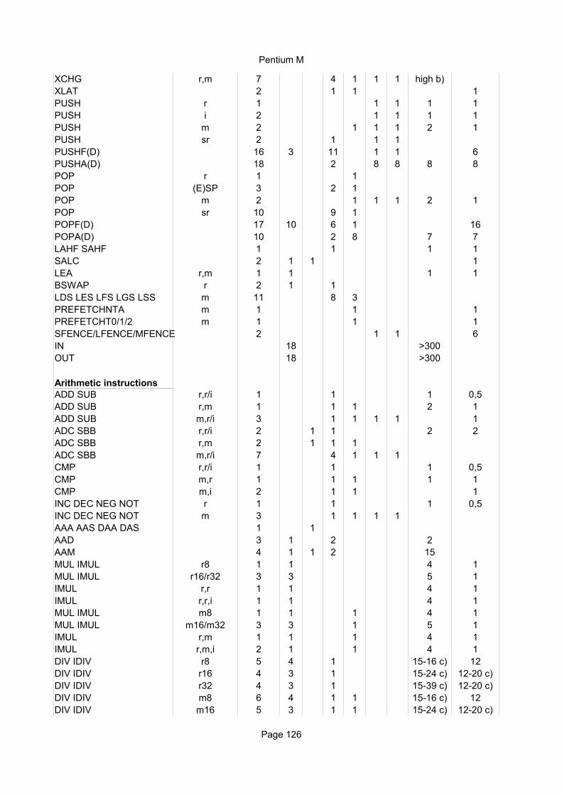
Pentium M
Page 126
XCHG r,m 7 4 1 1 1 high b)XLAT 2 1 1 1PUSH r 1 1 1 1 1PUSH i 2 1 1 1 1PUSH m 2 1 1 1 2 1PUSH sr 2 1 1 1PUSHF(D) 16 3 11 1 1 6PUSHA(D) 18 2 8 8 8 8POP r 1 1POP (E)SP 3 2 1POP m 2 1 1 1 2 1POP sr 10 9 1POPF(D) 17 10 6 1 16POPA(D) 10 2 8 7 7LAHF SAHF 1 1 1 1SALC 2 1 1 1LEA r,m 1 1 1 1BSWAP r 2 1 1LDS LES LFS LGS LSS m 11 8 3PREFETCHNTA m 1 1 1PREFETCHT0/1/2 m 1 1 1SFENCE/LFENCE/MFENCE 2 1 1 6IN 18 >300OUT 18 >300
Arithmetic instructionsADD SUB r,r/i 1 1 1 0,5ADD SUB r,m 1 1 1 2 1ADD SUB m,r/i 3 1 1 1 1 1ADC SBB r,r/i 2 1 1 2 2ADC SBB r,m 2 1 1 1ADC SBB m,r/i 7 4 1 1 1CMP r,r/i 1 1 1 0,5CMP m,r 1 1 1 1 1CMP m,i 2 1 1 1INC DEC NEG NOT r 1 1 1 0,5INC DEC NEG NOT m 3 1 1 1 1AAA AAS DAA DAS 1 1AAD 3 1 2 2AAM 4 1 1 2 15MUL IMUL r8 1 1 4 1MUL IMUL r16/r32 3 3 5 1IMUL r,r 1 1 4 1IMUL r,r,i 1 1 4 1MUL IMUL m8 1 1 1 4 1MUL IMUL m16/m32 3 3 1 5 1IMUL r,m 1 1 1 4 1IMUL r,m,i 2 1 1 4 1DIV IDIV r8 5 4 1 15-16 c) 12DIV IDIV r16 4 3 1 15-24 c) 12-20 c)DIV IDIV r32 4 3 1 15-39 c) 12-20 c)DIV IDIV m8 6 4 1 1 15-16 c) 12DIV IDIV m16 5 3 1 1 15-24 c) 12-20 c)

Pentium M
Page 127
DIV IDIV m32 5 3 1 1 15-39 c) 12-20 c)CBW CWDE 1 1 1 1CWD CDQ 1 1 1 1
Logic instructionsAND OR XOR r,r/i 1 1 1 0,5AND OR XOR r,m 1 1 1 2 1AND OR XOR m,r/i 3 1 1 1 1 1TEST r,r/i 1 1 1 0,5TEST m,r 1 1 1 1 1TEST m,i 2 1 1 1SHR SHL SAR ROR ROL r,i/CL 1 1 1 1SHR SHL SAR ROR ROL m,i/CL 3 1 1 1 1RCR RCL r,1 2 1 1 2 2RCR r8,i/CL 9 5 4 11RCL r8,i/CL 8 4 4 10RCR RCL r16/32,i/CL 6 3 3 9 9RCR RCL m,1 7 2 2 1 1 1RCR m8,i/CL 12 6 3 1 1 1RCL m8,i/CL 11 5 3 1 1 1RCR RCL m16/32,i/CL 10 5 2 1 1 1SHLD SHRD r,r,i/CL 2 2 2 2SHLD SHRD m,r,i/CL 4 1 1 1 1 1BT r,r/i 1 1 1 1BT m,r 8 7 1BT m,i 2 1 1BTR BTS BTC r,r/i 1 1BTR BTS BTC m,r 10 7 1 1 1 6BTR BTS BTC m,i 3 1 1 1 1BSF BSR r,r 2 1 1BSF BSR r,m 2 1 1 1SETcc r 1 1SETcc m 2 1 1 1CLC STC CMC 1 1 1CLD STD 4 4 7
Control transfer instructionsJMP short/near 1 1 1JMP far 22 21 1 28JMP r 1 1 1JMP m(near) 2 1 1 2JMP m(far) 25 23 2 31conditional jump short/near 1 1 1J(E)CXZ short 2 1 1 1LOOP short 11 2 1 8 6LOOP(N)E short 11 2 1 8 6CALL near 4 1 1 1 1 2CALL far 32 27 1 2 2 27CALL r 4 1 2 1 1 9CALL m(near) 4 1 1 1 1 2CALL m(far) 35 29 2 2 2 30RETN 2 1 2 1 2

Pentium M
Page 128
RETN i 3 1 1 1 2RETF 27 24 3 30RETF i 27 24 3 30BOUND r,m 15 7 6 2 8INTO 5 5 4
String instructionsLODS 2 2 4REP LODS 6n 10+6n 0,5STOS 3 1 1 1 1REP STOS 5n ca. 5n a) 0,7MOVS 6 1 3 1 1 0,7REP MOVS 6n ca. 6n a) 0,5SCAS 3 1 2 1,3REP(N)E SCAS 7n 12+7n 0,6CMPS 6 4 2 0,7REP(N)E CMPS 9n 12+9n 0,5
OtherNOP (90) 1 1 0,5Long NOP (0F 1F) 1 1 1PAUSE 2 2CLI 9STI 17ENTER i,0 12 10 1 1ENTER a,b ca. 18 +4b b-1 2bLEAVE 3 2 1CPUID 38-59 38-59 ca. 130RDTSC 13 13 42Notes:a)
b) Has an implicit LOCK prefix. c)
Floating point x87 instructionsInstruction Operands μops unfused domain Latency
p0 p1 p01 p2 p3 p4
Move instructions
FLD r 1 1 1FLD m32/64 1 1 1FLD m80 4 2 2FBLD m80 40 38 2FST(P) r 1 1FST(P) m32/m64 1 1 1 1FSTP m80 6 2 2 2 3FBSTP m80 169 165 2 2 167FXCH r 1 0 0.33 f)
Faster under certain conditions: see manual 3: "The microarchitecture of In-tel, AMD and VIA CPUs".
High values are typical, low values are for round divisors. Core Solo/Duo is more efficient than Pentium M in cases with round values that allow an early-out algorithm.
μops fused
domain
Recipro-cal
through-put

Pentium M
Page 129
FILD m 4 3 1 5 2FIST(P) m 4 2 1 1 5 2FISTTP g) m 4 2 1 1 5 2FLDZ 1 1FLD1 FLDPI FLDL2E etc. 2 2FCMOVcc r 2 2 2FNSTSW AX 3 3 7 3FNSTSW m16 2 1 1 1FLDCW m16 3 1 1 1 19FNSTCW m16 3 1 1 1 3FINCSTP FDECSTP 1 1 1FFREE r 1 1 1FFREEP r 2 2 2FNSAVE 142 142 131FRSTOR 72 72 91
Arithmetic instructionsFADD(P) FSUB(R)(P) r 1 1 3 1FADD(P) FSUB(R)(P) m 1 1 1 3 1FMUL(P) r 1 1 5 2FMUL(P) m 1 1 1 5 2FDIV(R)(P) r 1 1 9-38 c) 8-37 c)FDIV(R)(P) m 1 1 1 9-38 c) 8-37 c)FABS 1 1 1 1FCHS 1 1 1 1FCOM(P) FUCOM r 1 1 1 1FCOM(P) FUCOM m 1 1 1 1 1FCOMPP FUCOMPP 2 1 1 1 1FCOMI(P) FUCOMI(P) r 1 1 1 1FIADD FISUB(R) m 6 3 1 1 1 3 3FIMUL m 6 5 1 5 3FIDIV(R) m 6 5 1 9-38 c) 8-37 c)FICOM(P) m 6 3 2 1 4FTST 1 1 1FXAM 1 1 1FPREM FPREM1 26 26 37FRNDINT 15 15 19
MathFSCALE 28 28 43FXTRACT 15 15 9FSQRT 1 1 9 h) 8FSIN FCOS 80-100 80-100 80-110FSINCOS 90-110 90-110 100-130F2XM1 ~ 20 ~20 ~45FYL2X ~ 40 ~40 ~60FYL2XP1 ~ 55 ~55 ~65FPTAN ~ 100 ~100 ~140FPATAN ~ 85 ~85 ~140
OtherFNOP 1 1 1WAIT 2 1 1 1

Pentium M
Page 130
FNCLEX 3 3 13FNINIT 14 14 27Notes:c) High values are typical, low values are for low precision or round divisors.f)
g) SSE3 instruction only available on Core Solo and Core Duo.
Integer MMX and XMM instructionsInstruction Operands μops unfused domain Latency
p0 p1 p01 p2 p3 p4
Move instructions
MOVD r32,mm 1 1 1 0,5MOVD mm,r32 1 1 1 0,5MOVD mm,m32 1 1 1MOVD m32,mm 1 1 1 1MOVD r32,xmm 1 1 1 1MOVD xmm,r32 2 2 1MOVD xmm,m32 2 1 1 1MOVD m32, xmm 1 1 1 1MOVQ mm,mm 1 1 0,5MOVQ mm,m64 1 1 1MOVQ m64,mm 1 1 1 1MOVQ xmm,xmm 2 2 1 1MOVQ xmm,m64 2 1 1 1MOVQ m64, xmm 1 1 1 1MOVDQA xmm, xmm 2 2 1 1MOVDQA xmm, m128 2 2 2MOVDQA m128, xmm 2 2 2 2MOVDQU xmm, m128 4 2 2 2-10MOVDQU m128, xmm 8 5-6 2-3 2-3 4-20LDDQU g) xmm, m128 4 2MOVDQ2Q mm, xmm 1 1 1 1MOVQ2DQ xmm,mm 2 1 1 1 1MOVNTQ m64,mm 1 1 1 2MOVNTDQ m128,xmm 4 2 2 3
mm,mm 1 1 1 1
mm,m64 1 1 1 1 1
xmm,xmm 3 2 1 2 2
xmm,m128 4 1 1 2 2 2PUNPCKH/LBW/WD/DQ mm,mm 1 1 1 1PUNPCKH/LBW/WD/DQ mm,m64 1 1 1 1PUNPCKH/LBW/WD/DQ xmm,xmm 2 2 2 2PUNPCKH/LBW/WD/DQ xmm,m128 3 1 2 2PUNPCKHQDQ xmm,xmm 2 1 1 1 1PUNPCKHQDQ xmm, m128 3 1 2 1
FXCH generates 1 μop that is resolved by register renaming without going to any port.
μops fused
domain
Recipro-cal
through-put
PACKSSWB/DW PACKUSWB
PACKSSWB/DW PACKUSWB
PACKSSWB/DW PACKUSWB
PACKSSWB/DW PACKUSWB

Pentium M
Page 131
PUNPCKLQDQ xmm,xmm 1 1 1 1PUNPCKLQDQ xmm, m128 1 1 1PSHUFW mm,mm,i 1 1 1 1PSHUFW mm,m64,i 2 1 1 1PSHUFD xmm,xmm,i 3 2 1 2 2PSHUFD xmm,m128,i 4 1 1 2 2PSHUFL/HW xmm,xmm,i 2 1 1 1PSHUFL/HW xmm, m128,i 3 1 2 1MASKMOVQ mm,mm 3 1 1 1MASKMOVDQU xmm,xmm 8 1 2 2PMOVMSKB r32,mm 1 1 1 1PMOVMSKB r32,xmm 1 1 j) 1 1PEXTRW r32,mm,i 2 1 1 2 1PEXTRW r32,xmm,i 4 2 2 3 2PINSRW mm,r32,i 1 1 1 1PINSRW xmm,r32,i 2 2 1 2
Arithmetic instructionsPADD/SUB(U)(S)B/W/D mm,mm 1 1 1 0,5PADD/SUB(U)(S)B/W/D mm,m64 1 1 1 1PADD/SUB(U)(S)B/W/D xmm,xmm 2 2 1 1PADD/SUB(U)(S)B/W/D xmm,m128 4 2 2 2PADDQ PSUBQ mm,mm 2 2 2 1PADDQ PSUBQ mm,m64 2 2 1 1PADDQ PSUBQ xmm,xmm 4 4 2 2PADDQ PSUBQ xmm,m128 6 4 2 2PCMPEQ/GTB/W/D mm,mm 1 1 1 0,5PCMPEQ/GTB/W/D mm,m64 1 1 1 1PCMPEQ/GTB/W/D xmm,xmm 2 2 1 1PCMPEQ/GTB/W/D xmm,m128 2 2 2 2PMULL/HW PMULHUW mm,mm 1 1 3 1PMULL/HW PMULHUW mm,m64 1 1 1 3 1PMULL/HW PMULHUW xmm,xmm 2 2 3 2PMULL/HW PMULHUW xmm,m128 4 2 2 3 2PMULUDQ mm,mm 1 1 4 1PMULUDQ mm,m64 1 1 1 4 1PMULUDQ xmm,xmm 2 2 4 2PMULUDQ xmm,m128 4 2 2 4 2PMADDWD mm,mm 1 1 3 1PMADDWD mm,m64 1 1 1 3 1PMADDWD xmm,xmm 2 2 3 2PMADDWD xmm,m128 4 2 2 3 2PAVGB/W mm,mm 1 1 1 0,5PAVGB/W mm,m64 1 1 1 1PAVGB/W xmm,xmm 2 2 1 1PAVGB/W xmm,m128 4 2 2 2PMIN/MAXUB/SW mm,mm 1 1 1 0,5PMIN/MAXUB/SW mm,m64 1 1 1 1PMIN/MAXUB/SW xmm,xmm 2 2 1 1PMIN/MAXUB/SW xmm,m128 4 2 2 2PSADBW mm,mm 2 2 4 1PSADBW mm,m64 2 2 1 4 1PSADBW xmm,xmm 4 4 4 2

Pentium M
Page 132
PSADBW xmm,m128 6 4 2 4 2
Logic instructionsPAND(N) POR PXOR mm,mm 1 1 1 0,5PAND(N) POR PXOR mm,m64 1 1 1 1PAND(N) POR PXOR xmm,xmm 2 2 1 1PAND(N) POR PXOR xmm,m128 4 2 2 2PSLL/RL/RAW/D/Q mm,mm/i 1 1 1 1PSLL/RL/RAW/D/Q mm,m64 1 1 1 1PSLL/RL/RAW/D/Q xmm,i 2 2 2 2PSLL/RL/RAW/D/Q xmm,xmm 3 2 1 2 2PSLL/RL/RAW/D/Q xmm,m128 3 1 2 2PSLL/RLDQ xmm,i 4 3 1 3 3
OtherEMMS 11 11 6 k) 6Notes:g) SSE3 instruction only available on Core Solo and Core Duo.j) Also uses some execution units under port 1.k)
Floating point XMM instructionsInstruction Operands μops unfused domain Latency
p0 p1 p01 p2 p3 p4
Move instructions
MOVAPS/D xmm,xmm 2 2 1 1MOVAPS/D xmm,m128 2 2 2 2MOVAPS/D m128,xmm 2 2 2 3 2MOVUPS/D xmm,m128 4 4 2 2MOVUPS/D m128,xmm 8 4 2 2 3 4MOVSS/D xmm,xmm 1 1 1 1MOVSS/D xmm,m32/64 2 1 1 1 1MOVSS/D m32/64,xmm 1 1 1 1 1MOVHPS/D MOVLPS/D xmm,m64 1 1 1 1 1MOVHPS/D MOVLPS/D m64,xmm 1 1 1 1 1MOVLHPS MOVHLPS xmm,xmm 1 1 1 1MOVMSKPS/D r32,xmm 1 1 j) 2 1MOVNTPS/D m128,xmm 2 2 2 3SHUFPS/D xmm,xmm,i 3 2 1 2 2SHUFPS/D xmm,m128,i 4 1 1 2 2MOVDDUP g) xmm,xmm 2 1 1MOVSH/LDUP g) xmm,xmm 2 2 2MOVSH/LDUP g) xmm,m128 4UNPCKH/LPS xmm,xmm 4 2 2 3-4 5UNPCKH/LPS xmm,m128 4 2 2 5UNPCKH/LPD xmm,xmm 2 1 1 1 1UNPCKH/LPD xmm,m128 3 1 1 1 1
You may hide the delay by inserting other instructions between EMMS and any subsequent floating point instruction.
μops fused
domain
Recipro-cal
through-put
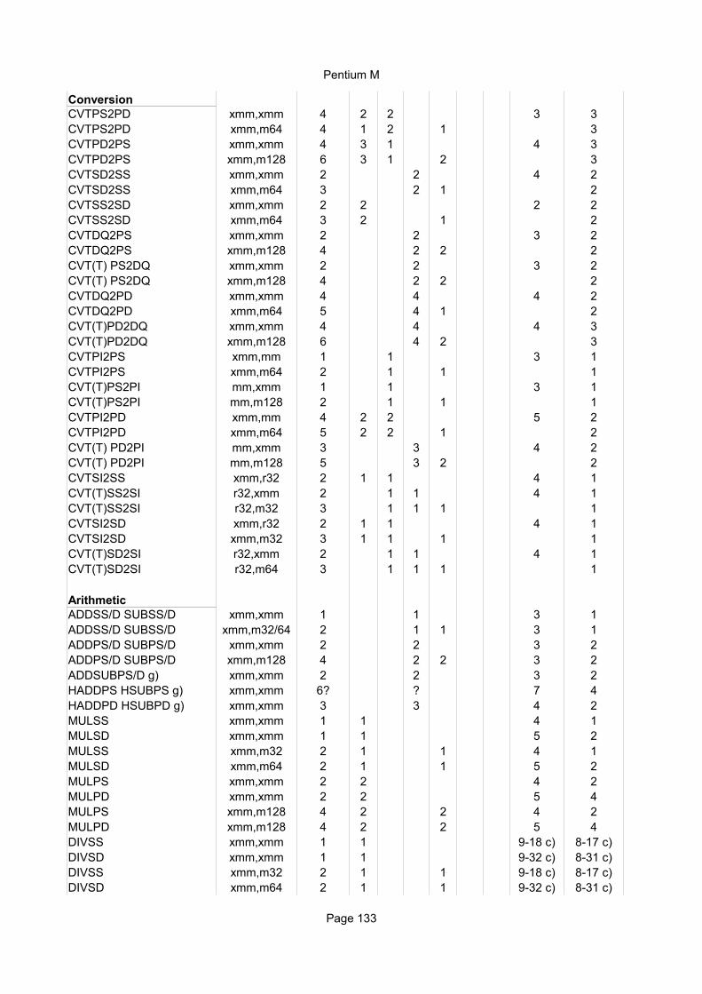
Pentium M
Page 133
ConversionCVTPS2PD xmm,xmm 4 2 2 3 3CVTPS2PD xmm,m64 4 1 2 1 3CVTPD2PS xmm,xmm 4 3 1 4 3CVTPD2PS xmm,m128 6 3 1 2 3CVTSD2SS xmm,xmm 2 2 4 2CVTSD2SS xmm,m64 3 2 1 2CVTSS2SD xmm,xmm 2 2 2 2CVTSS2SD xmm,m64 3 2 1 2CVTDQ2PS xmm,xmm 2 2 3 2CVTDQ2PS xmm,m128 4 2 2 2CVT(T) PS2DQ xmm,xmm 2 2 3 2CVT(T) PS2DQ xmm,m128 4 2 2 2CVTDQ2PD xmm,xmm 4 4 4 2CVTDQ2PD xmm,m64 5 4 1 2CVT(T)PD2DQ xmm,xmm 4 4 4 3CVT(T)PD2DQ xmm,m128 6 4 2 3CVTPI2PS xmm,mm 1 1 3 1CVTPI2PS xmm,m64 2 1 1 1CVT(T)PS2PI mm,xmm 1 1 3 1CVT(T)PS2PI mm,m128 2 1 1 1CVTPI2PD xmm,mm 4 2 2 5 2CVTPI2PD xmm,m64 5 2 2 1 2CVT(T) PD2PI mm,xmm 3 3 4 2CVT(T) PD2PI mm,m128 5 3 2 2CVTSI2SS xmm,r32 2 1 1 4 1CVT(T)SS2SI r32,xmm 2 1 1 4 1CVT(T)SS2SI r32,m32 3 1 1 1 1CVTSI2SD xmm,r32 2 1 1 4 1CVTSI2SD xmm,m32 3 1 1 1 1CVT(T)SD2SI r32,xmm 2 1 1 4 1CVT(T)SD2SI r32,m64 3 1 1 1 1
ArithmeticADDSS/D SUBSS/D xmm,xmm 1 1 3 1ADDSS/D SUBSS/D xmm,m32/64 2 1 1 3 1ADDPS/D SUBPS/D xmm,xmm 2 2 3 2ADDPS/D SUBPS/D xmm,m128 4 2 2 3 2ADDSUBPS/D g) xmm,xmm 2 2 3 2HADDPS HSUBPS g) xmm,xmm 6? ? 7 4HADDPD HSUBPD g) xmm,xmm 3 3 4 2MULSS xmm,xmm 1 1 4 1MULSD xmm,xmm 1 1 5 2MULSS xmm,m32 2 1 1 4 1MULSD xmm,m64 2 1 1 5 2MULPS xmm,xmm 2 2 4 2MULPD xmm,xmm 2 2 5 4MULPS xmm,m128 4 2 2 4 2MULPD xmm,m128 4 2 2 5 4DIVSS xmm,xmm 1 1 9-18 c) 8-17 c)DIVSD xmm,xmm 1 1 9-32 c) 8-31 c)DIVSS xmm,m32 2 1 1 9-18 c) 8-17 c)DIVSD xmm,m64 2 1 1 9-32 c) 8-31 c)

Pentium M
Page 134
DIVPS xmm,xmm 2 2 16-34 c) 16-34 c)DIVPD xmm,xmm 2 2 16-62 c) 16-62 c)DIVPS xmm,m128 4 2 2 16-34 c) 16-34 c)DIVPD xmm,m128 4 2 2 16-62 c) 16-62 c)CMPccSS/D xmm,xmm 1 1 3 1CMPccSS/D xmm,m32/64 2 1 1 1CMPccPS/D xmm,xmm 2 2 3 2CMPccPS/D xmm,m128 4 2 2 2COMISS/D UCOMISS/D xmm,xmm 1 1 1COMISS/D UCOMISS/D xmm,m32/64 2 1 1 1MAXSS/D MINSS/D xmm,xmm 1 1 3 1MAXSS/D MINSS/D xmm,m32/64 2 1 1 3 1MAXPS/D MINPS/D xmm,xmm 2 2 3 2MAXPS/D MINPS/D xmm,m128 4 2 2 3 2RCPSS xmm,xmm 1 1 3 1RCPSS xmm,m32 2 1 1 1RCPPS xmm,xmm 2 2 3 2RCPPS xmm,m128 4 2 2 2
MathSQRTSS xmm,xmm 2 2 6-30 4-28SQRTSS xmm,m32 3 2 1 4-28SQRTSD xmm,xmm 1 1 5-58 4-57SQRTSD xmm,m64 2 1 1 4-57SQRTPS xmm,xmm 2 2 8-56 16-55SQRTPD xmm,xmm 2 2 16-114 16-114SQRTPS xmm,m128 4 2 2 16-55SQRTPD xmm,m128 4 2 2 16-114RSQRTSS xmm,xmm 1 1 3 1RSQRTSS xmm,m32 2 1 1 1RSQRTPS xmm,xmm 2 3 3 2RSQRTPS xmm,m128 4 2 2 2
LogicAND/ANDN/OR/XORPS/D xmm,xmm 2 2 1 1AND/ANDN/OR/XORPS/D xmm,m128 4 2 2 1
OtherLDMXCSR m32 9 9 20STMXCSR m32 6 6 12FXSAVE m4096 118 32 43 43 63FXRSTOR m4096 87 43 44 72Notes:c) High values are typical, low values are for round divisors.g) SSE3 instruction only available on Core Solo and Core Duo.j) Also uses some execution units under port 1.

Merom
Page 135
Intel Core 2 (Merom, 65nm)List of instruction timings and μop breakdown
Explanation of column headings:Operands:
μops fused domain:
μops unfused domain:
p015: The total number of μops going to port 0, 1 and 5.p0: The number of μops going to port 0 (execution units).p1: The number of μops going to port 1 (execution units). p5: The number of μops going to port 5 (execution units). p2: The number of μops going to port 2 (memory read).p3: The number of μops going to port 3 (memory write address).p4: The number of μops going to port 4 (memory write data).Unit:
Latency:
Reciprocal throughput:
Integer instructionsInstruction Operands μops unfused domain Unit
p015 p0 p1 p5 p2 p3 p4
Move instructionsMOV r,r/i 1 1 x x x int 1 0,33
i = immediate data, r = register, mm = 64 bit mmx register, xmm = 128 bit xmm register, (x)mm = mmx or xmm register, sr = segment register, m = memory, m32 = 32-bit memory operand, etc.
The number of μops at the decode, rename, allocate and retirement stages in the pipeline. Fused μops count as one.
The number of μops for each execution port. Fused μops count as two. Fused macro-ops count as one. The instruction has μop fusion if the sum of the num-bers listed under p015 + p2 + p3 + p4 exceeds the number listed under μops fused domain. An x under p0, p1 or p5 means that at least one of the μops listed under p015 can optionally go to this port. For example, a 1 under p015 and an x under p0 and p5 means one μop which can go to either port 0 or port 5, whichever is vacant first. A value listed under p015 but nothing under p0, p1 and p5 means that it is not known which of the three ports these μops go to.
Tells which execution unit cluster is used. An additional delay of 1 clock cycle is generated if a register written by a μop in the integer unit (int) is read by a μop in the floating point unit (float) or vice versa. flt→int means that an instruc-tion with multiple μops receive the input in the float unit and delivers the output in the int unit. Delays for moving data between different units are included un-der latency when they are unavoidable. For example, movd eax,xmm0 has an extra 1 clock delay for moving from the XMM-integer unit to the general pur-pose integer unit. This is included under latency because it occurs regardless of which instruction comes next. Nothing listed under unit means that additional delays are either unlikely to occur or unavoidable and therefore included in the latency figure.This is the delay that the instruction generates in a dependency chain. The numbers are minimum values. Cache misses, misalignment, and exceptions may increase the clock counts considerably. Floating point operands are pre-sumed to be normal numbers. Denormal numbers, NAN's and infinity increase the delays very much, except in XMM move, shuffle and Boolean instructions. Floating point overflow, underflow, denormal or NAN results give a similar de-lay. The time unit used is core clock cycles, not the reference clock cycles given by the time stamp counter.
The average number of core clock cycles per instruction for a series of inde-pendent instructions of the same kind in the same thread.
μops fused do-main
Laten-cy
Reci-procal through-put

Merom
Page 136
MOV a) r,m 1 1 int 2 1MOV a) m,r 1 1 1 int 3 1MOV m,i 1 1 1 int 3 1MOV r,sr 1 1 int 1MOV m,sr 2 1 1 1 int 1MOV sr,r 8 4 x x x 4 int 16MOV sr,m 8 3 x x 5 int 16MOVNTI m,r 2 1 1 int 2
r,r 1 1 x x x int 1 0,33MOVSX MOVZX r,m 1 1 int 1CMOVcc r,r 2 2 x x x int 2 1CMOVcc r,m 2 2 x x x 1 intXCHG r,r 3 3 x x x int 2 2XCHG r,m 7 x 1 1 1 int high b)XLAT 2 1 1 int 4 1PUSH r 1 1 1 int 3 1PUSH i 1 1 1 int 1PUSH m 2 1 1 1 int 1PUSH sr 2 1 1 1 int 1PUSHF(D/Q) 17 15 x x x 1 1 int 7PUSHA(D) i) 18 9 1 8 int 8POP r 1 1 int 2 1POP (E/R)SP 4 3 1 intPOP m 2 1 1 1 int 1,5POP sr 10 9 1 int 17POPF(D/Q) 24 23 x x x 1 int 20POPA(D) i) 10 2 8 int 7LAHF SAHF 1 1 x x x int 1 0,33SALC i) 2 2 x x x int 4 1LEA a) r,m 1 1 1 int 1 1BSWAP r 2 2 1 1 int 4 1LDS LES LFS LGS LSS m 11 11 1 int 17PREFETCHNTA m 1 1 int 1PREFETCHT0/1/2 m 1 1 int 1LFENCE 2 1 1 int 8MFENCE 2 1 1 int 9SFENCE 2 1 1 int 9CLFLUSH m8 4 2 x x x 1 1 int 240 117IN intOUT int
Arithmetic instructionsADD SUB r,r/i 1 1 x x x int 1 0,33ADD SUB r,m 1 1 x x x 1 int 1ADD SUB m,r/i 2 1 x x x 1 1 1 int 6 1ADC SBB r,r/i 2 2 x x x int 2 2ADC SBB r,m 2 2 x x x 1 int 2 2ADC SBB m,r/i 4 3 x x x 1 1 1 int 7CMP r,r/i 1 1 x x x int 1 0,33CMP m,r/i 1 1 x x x 1 int 1 1INC DEC NEG NOT r 1 1 x x x int 1 0,33INC DEC NEG NOT m 3 1 x x x 1 1 1 int 6 1
MOVSX MOVZX MOVSXD

Merom
Page 137
AAA AAS DAA DAS i) 1 1 1 int 1AAD i) 3 3 x x x int 1AAM i) 4 4 int 17MUL IMUL r8 1 1 1 int 3 1MUL IMUL r16 3 3 x x x int 5 1,5MUL IMUL r32 3 3 x x x int 5 1,5MUL IMUL r64 3 3 x x x int 7 4IMUL r16,r16 1 1 1 int 3 1IMUL r32,r32 1 1 1 int 3 1IMUL r64,r64 1 1 1 int 5 2IMUL r16,r16,i 1 1 1 int 3 1IMUL r32,r32,i 1 1 1 int 3 1IMUL r64,r64,i 1 1 1 int 5 2MUL IMUL m8 1 1 1 1 int 3 1MUL IMUL m16 3 3 x x x 1 int 5 1,5MUL IMUL m32 3 3 x x x 1 int 5 1,5MUL IMUL m64 3 2 2 1 int 7 4IMUL r16,m16 1 1 1 1 int 3 1IMUL r32,m32 1 1 1 1 int 3 1IMUL r64,m64 1 1 1 1 int 5 2IMUL r16,m16,i 1 1 1 1 int 2IMUL r32,m32,i 1 1 1 1 int 1IMUL r64,m64,i 1 1 1 1 int 2DIV IDIV r8 3 3 int 18 12DIV IDIV r16 5 5 int 18-26 12-20 c)DIV IDIV r32 4 4 int 18-42 12-36 c)DIV r64 32 32 int 29-61 18-37 c)IDIV r64 56 56 int 39-72 28-40 c)DIV IDIV m8 4 3 1 int 18 12DIV IDIV m16 6 5 1 int 18-26 12-20 c)DIV IDIV m32 5 4 1 int 18-42 12-36 c)DIV m64 32 31 1 int 29-61 18-37 c)IDIV m64 56 55 1 int 39-72 28-40 c)CBW CWDE CDQE 1 1 x x x int 1CWD CDQ CQO 1 1 x x int 1
Logic instructionsAND OR XOR r,r/i 1 1 x x x int 1 0,33AND OR XOR r,m 1 1 x x x 1 int 1AND OR XOR m,r/i 2 1 x x x 1 1 1 int 6 1TEST r,r/i 1 1 x x x int 1 0,33TEST m,r/i 1 1 x x x 1 int 1SHR SHL SAR r,i/cl 1 1 x x int 1 0,5SHR SHL SAR m,i/cl 3 2 x x 1 1 1 int 6 1ROR ROL r,i/cl 1 1 x x int 1 1ROR ROL m,i/cl 3 2 x x 1 1 1 int 6 1RCR RCL r,1 2 2 x x x int 2 2RCR r8,i/cl 9 9 x x x int 12RCL r8,i/cl 8 8 x x x int 11RCR RCL r16/32/64,i/cl 6 6 x x x int 11RCR RCL m,1 4 3 x x x 1 1 1 int 7RCR m8,i/cl 12 9 x x x 1 1 1 int 14RCL m8,i/cl 11 8 x x x 1 1 1 int 13

Merom
Page 138
RCR RCL m16/32/64,i/cl 10 7 x x x 1 1 1 int 13SHLD SHRD r,r,i/cl 2 2 x x x int 2 1SHLD SHRD m,r,i/cl 3 2 x x x 1 1 1 int 7BT r,r/i 1 1 x x x int 1 1BT m,r 10 9 x x x 1 int 5BT m,i 2 1 x x x 1 int 1BTR BTS BTC r,r/i 1 1 x x x int 1BTR BTS BTC m,r 11 8 x x x 1 1 1 int 5BTR BTS BTC m,i 3 1 x x x 1 1 1 int 6BSF BSR r,r 2 2 x 1 x int 2 1BSF BSR r,m 2 2 x 1 x 1 int 2SETcc r 1 1 x x x int 1 1SETcc m 2 1 x x x 1 1 int 1CLC STC CMC 1 1 x x x int 1 0,33CLD 7 7 x x x int 4STD 6 6 x x x int 14
Control transfer instructionsJMP short/near 1 1 1 int 0 1-2JMP i) far 30 30 int 76JMP r 1 1 1 int 0 1-2JMP m(near) 1 1 1 1 int 0 1-2JMP m(far) 31 29 2 int 68Conditional jump short/near 1 1 1 int 0 1Fused compare/test and branch e,i) 1 1 1 int 0 1J(E/R)CXZ short 2 2 x x 1 int 1-2LOOP short 11 11 x x x int 5LOOP(N)E short 11 11 x x x int 5CALL near 3 2 x x x 1 1 int 2CALL i) far 43 43 int 75CALL r 3 2 1 1 int 2CALL m(near) 4 3 1 1 1 int 2CALL m(far) 44 42 2 int 75RETN 1 1 1 1 int 2RETN i 3 x 1 1 int 2RETF 32 30 2 int 78RETF i 32 30 2 int 78BOUND i) r,m 15 13 2 int 8INTO i) 5 5 int 3
String instructionsLODS 3 2 1 int 1REP LODS 4+7n - 14+6n int 1+5n - 21+3nSTOS 4 2 1 1 int 1REP STOS 8+5n - 20+1.2n int 7+2n - 0.55nMOVS 8 5 int
1 1 1 5 intREP MOVS 7+7n - 13+n int 1+3n - 0.63nSCAS 4 3 1 int 1REP(N)E SCAS 7+8n - 17+7n int 3+8n - 23+6nCMPS 7 5 2 int 3REP(N)E CMPS 7+10n - 7+9n int 2+7n - 22+5n
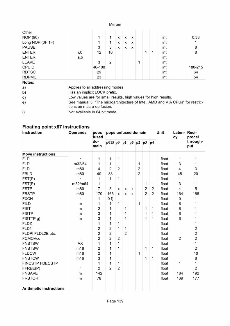
Merom
Page 139
OtherNOP (90) 1 1 x x x int 0,33Long NOP (0F 1F) 1 1 x x x int 1PAUSE 3 3 x x x int 8ENTER i,0 12 10 1 1 int 8ENTER a,b intLEAVE 3 2 1 intCPUID 46-100 int 180-215RDTSC 29 int 64RDPMC 23 int 54Notes:a) Applies to all addressing modesb) Has an implicit LOCK prefix. c) Low values are for small results, high values for high results.e)
i) Not available in 64 bit mode.
Floating point x87 instructionsInstruction Operands μops unfused domain Unit
p015 p0 p1 p5 p2 p3 p4
Move instructionsFLD r 1 1 1 float 1 1FLD m32/64 1 1 1 float 3 1FLD m80 4 2 2 2 float 4 3FBLD m80 40 38 2 float 45 20FST(P) r 1 1 1 float 1 1FST(P) m32/m64 1 1 1 float 3 1FSTP m80 7 3 x x x 2 2 float 4 5FBSTP m80 170 166 x x x 2 2 float 164 166FXCH r 1 0 f) float 0 1FILD m 1 1 1 1 float 6 1FIST m 2 1 1 1 1 float 6 1FISTP m 3 1 1 1 1 float 6 1FISTTP g) m 3 1 1 1 1 float 6 1FLDZ 1 1 1 float 1FLD1 2 2 1 1 float 2FLDPI FLDL2E etc. 2 2 2 float 2FCMOVcc r 2 2 2 float 2 2FNSTSW AX 1 1 1 float 1FNSTSW m16 2 1 1 1 1 float 2FLDCW m16 2 1 1 float 10FNSTCW m16 3 1 1 1 float 8FINCSTP FDECSTP 1 1 1 float 1 1FFREE(P) r 2 2 2 float 2FNSAVE m 142 float 184 192FRSTOR m 78 float 169 177
Arithmetic instructions
See manual 3: "The microarchitecture of Intel, AMD and VIA CPUs" for restric-tions on macro-op fusion.
μops fused do-main
Laten-cy
Reci-procal through-put

Merom
Page 140
FADD(P) FSUB(R)(P) r 1 1 1 float 3 1FADD(P) FSUB(R)(P) m 1 1 1 1 float 1FMUL(P) r 1 1 1 float 5 2FMUL(P) m 1 1 1 1 float 2FDIV(R)(P) r 1 1 1 float 6-38 d) 5-37 d)FDIV(R)(P) m 1 1 1 1 float 5-37 d)FABS 1 1 1 float 1 1FCHS 1 1 1 float 1 1FCOM(P) FUCOM r 1 1 1 float 1FCOM(P) FUCOM m 1 1 1 1 float 1FCOMPP FUCOMPP 2 2 1 1 floatFCOMI(P) FUCOMI(P) r 1 1 1 float 1FIADD FISUB(R) m 2 2 1 1 1 float 2FIMUL m 2 2 2 1 float 2FIDIV(R) m 2 2 2 1 float 5-37 d)FICOM(P) m 2 2 1 1 1 float 2FTST 1 1 1 float 1FXAM 1 1 1 float 1FPREM FPREM1 21-27 21-27 float 16-56FRNDINT 7-15 7-15 float 22-29
MathFSCALE 27 27 float 41FXTRACT 82 82 float 170FSQRT 1 1 float 6-69FSIN FCOS ~96 ~96 float ~96FSINCOS ~100 ~100 float ~115F2XM1 ~19 ~19 float ~45FYL2X FYL2XP1 ~53 ~53 float ~96FPTAN ~98 ~98 float ~136FPATAN ~70 ~70 float ~119
OtherFNOP 1 1 1 float 1WAIT 2 2 float 1FNCLEX 4 4 float 15FNINIT 15 15 float 63Notes:d) Round divisors or low precision give low values.f) Resolved by register renaming. Generates no μops in the unfused domain.g) SSE3 instruction set.
Integer MMX and XMM instructionsInstruction Operands μops unfused domain Unit
p015 p0 p1 p5 p2 p3 p4
Move instructionsMOVD k) r32/64,(x)mm 1 1 x x x int 2 0,33MOVD k) m32/64,(x)mm 1 1 1 3 1MOVD k) (x)mm,r32/64 1 1 x x int 2 0,5MOVD k) (x)mm,m32/64 1 1 int 2 1
μops fused do-main
Laten-cy
Reci-procal through-put
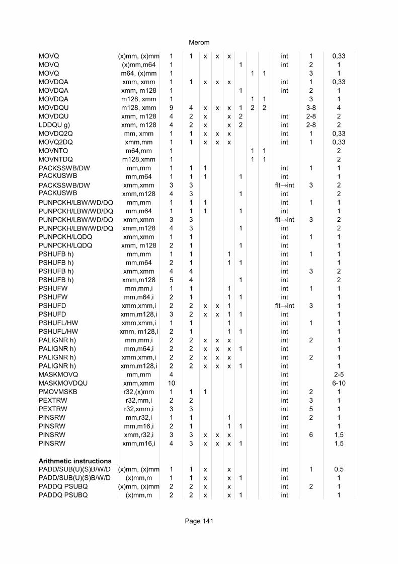
Merom
Page 141
MOVQ (x)mm, (x)mm 1 1 x x x int 1 0,33MOVQ (x)mm,m64 1 1 int 2 1MOVQ m64, (x)mm 1 1 1 3 1MOVDQA xmm, xmm 1 1 x x x int 1 0,33MOVDQA xmm, m128 1 1 int 2 1MOVDQA m128, xmm 1 1 1 3 1MOVDQU m128, xmm 9 4 x x x 1 2 2 3-8 4MOVDQU xmm, m128 4 2 x x 2 int 2-8 2LDDQU g) xmm, m128 4 2 x x 2 int 2-8 2MOVDQ2Q mm, xmm 1 1 x x x int 1 0,33MOVQ2DQ xmm,mm 1 1 x x x int 1 0,33MOVNTQ m64,mm 1 1 1 2MOVNTDQ m128,xmm 1 1 1 2
mm,mm 1 1 1 int 1 1mm,m64 1 1 1 1 int 1
xmm,xmm 3 3 flt→int 3 2xmm,m128 4 3 1 int 2
PUNPCKH/LBW/WD/DQ mm,mm 1 1 1 int 1 1PUNPCKH/LBW/WD/DQ mm,m64 1 1 1 1 int 1PUNPCKH/LBW/WD/DQ xmm,xmm 3 3 flt→int 3 2PUNPCKH/LBW/WD/DQ xmm,m128 4 3 1 int 2PUNPCKH/LQDQ xmm,xmm 1 1 int 1 1PUNPCKH/LQDQ xmm, m128 2 1 1 int 1PSHUFB h) mm,mm 1 1 1 int 1 1PSHUFB h) mm,m64 2 1 1 1 int 1PSHUFB h) xmm,xmm 4 4 int 3 2PSHUFB h) xmm,m128 5 4 1 int 2PSHUFW mm,mm,i 1 1 1 int 1 1PSHUFW mm,m64,i 2 1 1 1 int 1PSHUFD xmm,xmm,i 2 2 x x 1 flt→int 3 1PSHUFD xmm,m128,i 3 2 x x 1 1 int 1PSHUFL/HW xmm,xmm,i 1 1 1 int 1 1PSHUFL/HW xmm, m128,i 2 1 1 1 int 1PALIGNR h) mm,mm,i 2 2 x x x int 2 1PALIGNR h) mm,m64,i 2 2 x x x 1 int 1PALIGNR h) xmm,xmm,i 2 2 x x x int 2 1PALIGNR h) xmm,m128,i 2 2 x x x 1 int 1MASKMOVQ mm,mm 4 int 2-5MASKMOVDQU xmm,xmm 10 int 6-10PMOVMSKB r32,(x)mm 1 1 1 int 2 1PEXTRW r32,mm,i 2 2 int 3 1PEXTRW r32,xmm,i 3 3 int 5 1PINSRW mm,r32,i 1 1 1 int 2 1PINSRW mm,m16,i 2 1 1 1 int 1PINSRW xmm,r32,i 3 3 x x x int 6 1,5PINSRW xmm,m16,i 4 3 x x x 1 int 1,5
Arithmetic instructionsPADD/SUB(U)(S)B/W/D (x)mm, (x)mm 1 1 x x int 1 0,5PADD/SUB(U)(S)B/W/D (x)mm,m 1 1 x x 1 int 1PADDQ PSUBQ (x)mm, (x)mm 2 2 x x int 2 1PADDQ PSUBQ (x)mm,m 2 2 x x 1 int 1
PACKSSWB/DW PACKUSWB
PACKSSWB/DW PACKUSWB

Merom
Page 142
mm,mm 5 5 int 5 4
mm,m64 6 5 1 int 4
xmm,xmm 7 7 int 6 4
xmm,m128 8 7 1 int 4PHADDD PHSUBD h) mm,mm 3 3 int 3 2PHADDD PHSUBD h) mm,m64 4 3 1 int 2PHADDD PHSUBD h) xmm,xmm 5 5 int 5 3PHADDD PHSUBD h) xmm,m128 6 5 1 int 3PCMPEQ/GTB/W/D (x)mm,(x)mm 1 1 x x int 1 0,5PCMPEQ/GTB/W/D (x)mm,m 1 1 x x 1 int 1PMULL/HW PMULHUW (x)mm,(x)mm 1 1 1 int 3 1PMULL/HW PMULHUW (x)mm,m 1 1 1 1 int 1PMULHRSW h) (x)mm,(x)mm 1 1 1 int 3 1PMULHRSW h) (x)mm,m 1 1 1 1 int 1PMULUDQ (x)mm,(x)mm 1 1 1 int 3 1PMULUDQ (x)mm,m 1 1 1 1 int 1PMADDWD (x)mm,(x)mm 1 1 1 int 3 1PMADDWD (x)mm,m 1 1 1 1 int 1PMADDUBSW h) (x)mm,(x)mm 1 1 1 int 3 1PMADDUBSW h) (x)mm,m 1 1 1 1 int 1PAVGB/W (x)mm,(x)mm 1 1 x x int 1 0,5PAVGB/W (x)mm,m 1 1 x x 1 int 1PMIN/MAXUB/SW (x)mm,(x)mm 1 1 x x int 1 0,5PMIN/MAXUB/SW (x)mm,m 1 1 x x 1 int 1
(x)mm,(x)mm 1 1 x x int 1 0,5(x)mm,m 1 1 x x 1 int 1
(x)mm,(x)mm 1 1 x x int 1 0,5(x)mm,m 1 1 x x 1 int 1
PSADBW (x)mm,(x)mm 1 1 1 int 3 1PSADBW (x)mm,m 1 1 1 1 int 1
Logic instructionsPAND(N) POR PXOR (x)mm,(x)mm 1 1 x x x int 1 0,33PAND(N) POR PXOR (x)mm,m 1 1 x x x 1 int 1PSLL/RL/RAW/D/Q mm,mm/i 1 1 1 int 1 1PSLL/RL/RAW/D/Q mm,m64 1 1 1 1 int 1PSLL/RL/RAW/D/Q xmm,i 1 1 1 int 1 1PSLL/RL/RAW/D/Q xmm,xmm 2 2 x x int 2 1PSLL/RL/RAW/D/Q xmm,m128 3 2 x x 1 int 1PSLL/RLDQ xmm,i 2 2 x x int 2 1
OtherEMMS 11 11 x x x float 6Notes:g) SSE3 instruction set.h) Supplementary SSE3 instruction set.
k)
PHADD(S)W PHSUB(S)W h)
PHADD(S)W PHSUB(S)W h)
PHADD(S)W PHSUB(S)W h)
PHADD(S)W PHSUB(S)W h)
PABSB PABSW PABSD h)
PSIGNB PSIGNW PSIGND h)
MASM uses the name MOVD rather than MOVQ for this instruction even when moving 64 bits.

Merom
Page 143
Floating point XMM instructionsInstruction Operands μops unfused domain Unit
p015 p0 p1 p5 p2 p3 p4
Move instructionsMOVAPS/D xmm,xmm 1 1 x x x int 1 0,33MOVAPS/D xmm,m128 1 1 int 2 1MOVAPS/D m128,xmm 1 1 1 3 1MOVUPS/D xmm,m128 4 2 1 1 2 int 2-4 2MOVUPS/D m128,xmm 9 4 x x x 1 2 2 3-4 4MOVSS/D xmm,xmm 1 1 x x x int 1 0,33MOVSS/D xmm,m32/64 1 1 int 2 1MOVSS/D m32/64,xmm 1 1 1 3 1MOVHPS/D MOVLPS/D xmm,m64 2 1 1 1 int 3 1MOVHPS/D m64,xmm 2 1 1 1 1 5 1MOVLPS/D m64,xmm 1 1 1 3 1MOVLHPS MOVHLPS xmm,xmm 1 1 1 float 1 1MOVMSKPS/D r32,xmm 1 1 1 float 1 1MOVNTPS/D m128,xmm 1 1 1 2-3SHUFPS xmm,xmm,i 3 3 3 flt→int 3 2SHUFPS xmm,m128,i 4 3 3 1 flt→int 2SHUFPD xmm,xmm,i 1 1 1 float 1 1SHUFPD xmm,m128,i 2 1 1 1 float 1MOVDDUP g) xmm,xmm 1 1 1 int 1 1MOVDDUP g) xmm,m64 2 1 1 1 int 1MOVSH/LDUP g) xmm,xmm 1 1 1 int 1 1MOVSH/LDUP g) xmm,m128 2 1 1 1 int 1UNPCKH/LPS xmm,xmm 3 3 3 flt→int 3 2UNPCKH/LPS xmm,m128 4 3 3 1 int 2UNPCKH/LPD xmm,xmm 1 1 1 float 1 1UNPCKH/LPD xmm,m128 2 1 1 1 float 1
ConversionCVTPD2PS xmm,xmm 2 2 float 4 1CVTPD2PS xmm,m128 2 2 1 float 1CVTSD2SS xmm,xmm 2 2 float 4 1CVTSD2SS xmm,m64 2 2 1 float 1CVTPS2PD xmm,xmm 2 2 2 float 2 2CVTPS2PD xmm,m64 2 2 2 1 float 2CVTSS2SD xmm,xmm 2 2 float 2 2CVTSS2SD xmm,m32 2 2 2 1 float 2CVTDQ2PS xmm,xmm 1 1 1 float 3 1CVTDQ2PS xmm,m128 1 1 1 1 float 1CVT(T) PS2DQ xmm,xmm 1 1 1 float 3 1CVT(T) PS2DQ xmm,m128 1 1 1 1 float 1CVTDQ2PD xmm,xmm 2 2 1 1 float 4 1CVTDQ2PD xmm,m64 3 2 1 float 1CVT(T)PD2DQ xmm,xmm 2 2 float 4 1CVT(T)PD2DQ xmm,m128 2 2 1 float 1
μops fused do-main
Laten-cy
Reci-procal through-put

Merom
Page 144
CVTPI2PS xmm,mm 1 1 1 float 3 3CVTPI2PS xmm,m64 1 1 1 1 float 3CVT(T)PS2PI mm,xmm 1 1 1 float 3 1CVT(T)PS2PI mm,m128 1 1 1 1 float 1CVTPI2PD xmm,mm 2 2 1 1 float 4 1CVTPI2PD xmm,m64 2 2 1 1 1 float 1CVT(T) PD2PI mm,xmm 2 2 1 1 float 4 1CVT(T) PD2PI mm,m128 2 2 1 1 1 float 1CVTSI2SS xmm,r32 1 1 1 float 4 3CVTSI2SS xmm,m32 1 1 1 1 float 3CVT(T)SS2SI r32,xmm 1 1 1 float 3 1CVT(T)SS2SI r32,m32 1 1 1 1 float 1CVTSI2SD xmm,r32 2 2 1 1 float 4 3CVTSI2SD xmm,m32 2 1 1 1 float 3CVT(T)SD2SI r32,xmm 1 1 1 float 3 1CVT(T)SD2SI r32,m64 1 1 1 1 float 1
ArithmeticADDSS/D SUBSS/D xmm,xmm 1 1 1 float 3 1ADDSS/D SUBSS/D xmm,m32/64 1 1 1 1 float 1ADDPS/D SUBPS/D xmm,xmm 1 1 1 float 3 1ADDPS/D SUBPS/D xmm,m128 1 1 1 1 float 1ADDSUBPS/D g) xmm,xmm 1 1 1 float 3 1ADDSUBPS/D g) xmm,m128 1 1 1 1 float 1HADDPS HSUBPS g) xmm,xmm 6 6 float 9 3HADDPS HSUBPS g) xmm,m128 7 6 1 float 3HADDPD HSUBPD g) xmm,xmm 3 3 float 5 2HADDPD HSUBPD g) xmm,m128 4 3 1 float 2MULSS xmm,xmm 1 1 1 float 4 1MULSS xmm,m32 1 1 1 1 float 1MULSD xmm,xmm 1 1 1 float 5 1MULSD xmm,m64 1 1 1 1 float 1MULPS xmm,xmm 1 1 1 float 4 1MULPS xmm,m128 1 1 1 1 float 1MULPD xmm,xmm 1 1 1 float 5 1MULPD xmm,m128 1 1 1 1 float 1DIVSS xmm,xmm 1 1 1 float 6-18 d) 5-17 d)DIVSS xmm,m32 1 1 1 1 float 5-17 d)DIVSD xmm,xmm 1 1 1 float 6-32 d) 5-31 d)DIVSD xmm,m64 1 1 1 1 float 5-31 d)DIVPS xmm,xmm 1 1 1 float 6-18 d) 5-17 d)DIVPS xmm,m128 1 1 1 1 float 5-17 d)DIVPD xmm,xmm 1 1 1 float 6-32 d) 5-31 d)DIVPD xmm,m128 1 1 1 1 float 5-31 d)RCPSS/PS xmm,xmm 1 1 1 float 3 2RCPSS/PS xmm,m 1 1 1 1 float 2CMPccSS/D xmm,xmm 1 1 1 float 3 1CMPccSS/D xmm,m32/64 1 1 1 1 float 1CMPccPS/D xmm,xmm 1 1 1 float 3 1CMPccPS/D xmm,m128 1 1 1 1 float 1COMISS/D UCOMISS/D xmm,xmm 1 1 1 float 3 1COMISS/D UCOMISS/D xmm,m32/64 1 1 1 1 float 1MAXSS/D MINSS/D xmm,xmm 1 1 1 float 3 1
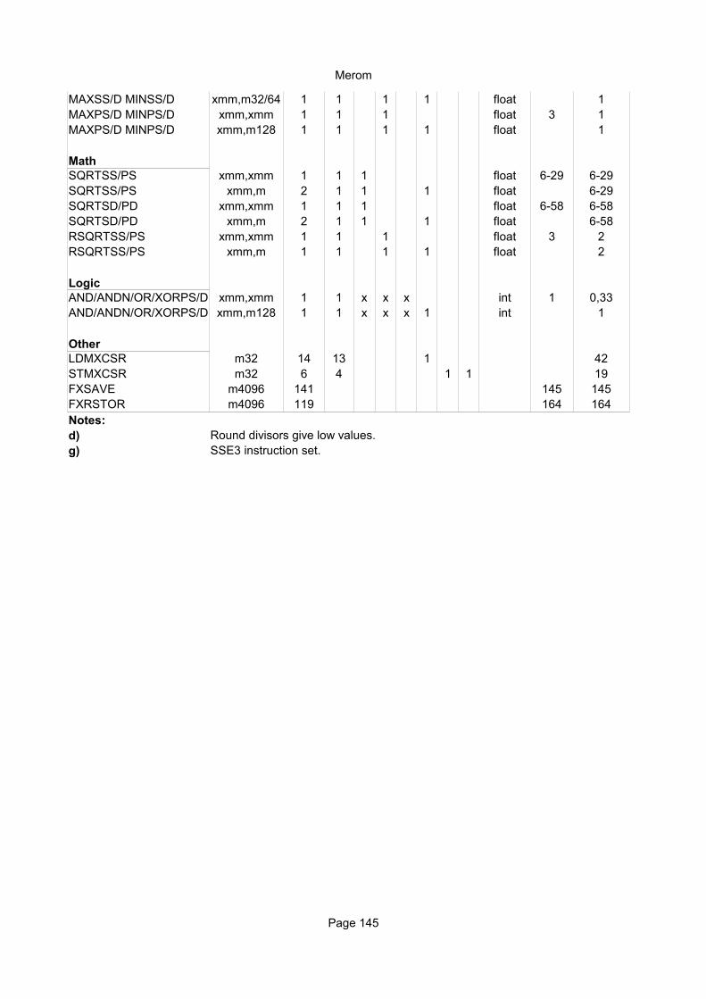
Merom
Page 145
MAXSS/D MINSS/D xmm,m32/64 1 1 1 1 float 1MAXPS/D MINPS/D xmm,xmm 1 1 1 float 3 1MAXPS/D MINPS/D xmm,m128 1 1 1 1 float 1
MathSQRTSS/PS xmm,xmm 1 1 1 float 6-29 6-29SQRTSS/PS xmm,m 2 1 1 1 float 6-29SQRTSD/PD xmm,xmm 1 1 1 float 6-58 6-58SQRTSD/PD xmm,m 2 1 1 1 float 6-58RSQRTSS/PS xmm,xmm 1 1 1 float 3 2RSQRTSS/PS xmm,m 1 1 1 1 float 2
LogicAND/ANDN/OR/XORPS/D xmm,xmm 1 1 x x x int 1 0,33AND/ANDN/OR/XORPS/D xmm,m128 1 1 x x x 1 int 1
OtherLDMXCSR m32 14 13 1 42STMXCSR m32 6 4 1 1 19FXSAVE m4096 141 145 145FXRSTOR m4096 119 164 164Notes:d) Round divisors give low values.g) SSE3 instruction set.

Wolfdale
Page 146
Intel Core 2 (Wolfdale, 45nm)List of instruction timings and μop breakdown
Explanation of column headings:Operands:
μops fused domain:
μops unfused domain:
p015: The total number of μops going to port 0, 1 and 5.p0: The number of μops going to port 0 (execution units).p1: The number of μops going to port 1 (execution units). p5: The number of μops going to port 5 (execution units). p2: The number of μops going to port 2 (memory read).p3: The number of μops going to port 3 (memory write address).p4: The number of μops going to port 4 (memory write data).Unit:
Latency:
Reciprocal throughput:
Integer instructionsInstruction Operands μops unfused domain Unit
p015 p0 p1 p5 p2 p3 p4
Move instructions
i = immediate data, r = register, mm = 64 bit mmx register, xmm = 128 bit xmm register, (x)mm = mmx or xmm register, sr = segment register, m = memory, m32 = 32-bit memory operand, etc.
The number of μops at the decode, rename, allocate and retirement stages in the pipeline. Fused μops count as one.
The number of μops for each execution port. Fused μops count as two. Fused macro-ops count as one. The instruction has μop fusion if the sum of the numbers listed under p015 + p2 + p3 + p4 exceeds the number listed under μops fused domain. An x under p0, p1 or p5 means that at least one of the μops listed under p015 can optionally go to this port. For example, a 1 under p015 and an x under p0 and p5 means one μop which can go to either port 0 or port 5, whichever is vacant first. A value listed under p015 but nothing un-der p0, p1 and p5 means that it is not known which of the three ports these μops go to.
Tells which execution unit cluster is used. An additional delay of 1 clock cycle is generated if a register written by a μop in the integer unit (int) is read by a μop in the floating point unit (float) or vice versa. flt→int means that an instruc-tion with multiple μops receive the input in the float unit and delivers the out-put in the int unit. Delays for moving data between different units are included under latency when they are unavoidable. For example, movd eax,xmm0 has an extra 1 clock delay for moving from the XMM-integer unit to the general purpose integer unit. This is included under latency because it occurs regard-less of which instruction comes next. Nothing listed under unit means that ad-ditional delays are either unlikely to occur or unavoidable and therefore in-cluded in the latency figure.
This is the delay that the instruction generates in a dependency chain. The numbers are minimum values. Cache misses, misalignment, and exceptions may increase the clock counts considerably. Floating point operands are pre-sumed to be normal numbers. Denormal numbers, NAN's and infinity increase the delays very much, except in XMM move, shuffle and Boolean instructions. Floating point overflow, underflow, denormal or NAN results give a similar de-lay. The time unit used is core clock cycles, not the reference clock cycles given by the time stamp counter.
The average number of core clock cycles per instruction for a series of inde-pendent instructions of the same kind in the same thread.
μops fused do-main
Laten-cy
Reci-procal through-put

Wolfdale
Page 147
MOV r,r/i 1 1 x x x 1 0,33MOV a) r,m 1 1 2 1MOV a) m,r 1 1 1 3 1MOV m,i 1 1 1 3 1MOV r,sr 1 1 1MOV m,sr 2 1 1 1 1MOV sr,r 8 4 x x x 4 16MOV sr,m 8 3 x x 5 16MOVNTI m,r 2 1 1 2
r,r 1 1 x x x 1 0,33MOVSX MOVZX r16/32,m 1 1 1MOVSX MOVSXD r64,m 2 1 x x x 1 1CMOVcc r,r 2 2 x x x 2 1CMOVcc r,m 2 2 x x x 1XCHG r,r 3 3 x x x 2 2XCHG r,m 7 x 1 1 1 high b)XLAT 2 1 1 4 1PUSH r 1 1 1 3 1PUSH i 1 1 1 1PUSH m 2 1 1 1 1PUSH sr 2 1 1 1 1PUSHF(D/Q) 17 15 x x x 1 1 7PUSHA(D) i) 18 9 1 8 8POP r 1 1 2 1POP (E/R)SP 4 3 1POP m 2 1 1 1 1,5POP sr 10 9 1 17POPF(D/Q) 24 23 x x x 1 20POPA(D) i) 10 2 8 7LAHF SAHF 1 1 x x x 1 0,33SALC i) 2 2 x x x 4 1LEA a) r,m 1 1 1 1 1BSWAP r 2 2 1 1 4 1LDS LES LFS LGS LSS m 11 11 1 17PREFETCHNTA m 1 1 1PREFETCHT0/1/2 m 1 1 1LFENCE 2 1 1 8MFENCE 2 1 1 6SFENCE 2 1 1 9CLFLUSH m8 4 2 1 1 1 1 120 90INOUT
Arithmetic instructionsADD SUB r,r/i 1 1 x x x 1 0,33ADD SUB r,m 1 1 x x x 1 1ADD SUB m,r/i 2 1 x x x 1 1 1 6 1ADC SBB r,r/i 2 2 x x x 2 2ADC SBB r,m 2 2 x x x 1 2 2ADC SBB m,r/i 4 3 x x x 1 1 1 7CMP r,r/i 1 1 x x x 1 0,33CMP m,r/i 1 1 x x x 1 1 1
MOVSX MOVZX MOVSXD
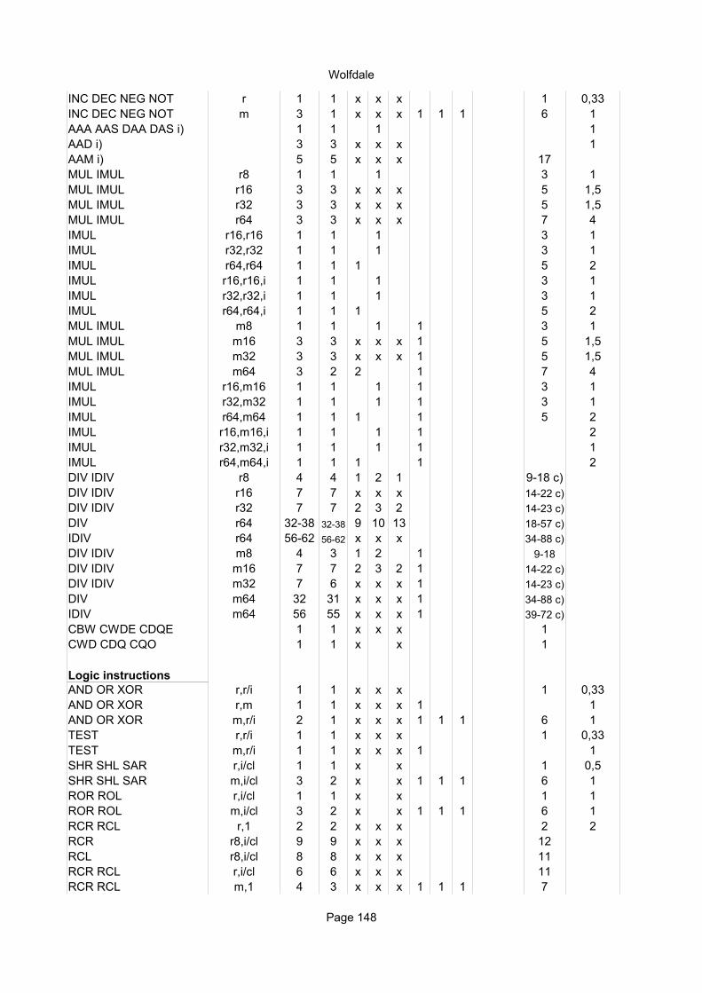
Wolfdale
Page 148
INC DEC NEG NOT r 1 1 x x x 1 0,33INC DEC NEG NOT m 3 1 x x x 1 1 1 6 1AAA AAS DAA DAS i) 1 1 1 1AAD i) 3 3 x x x 1AAM i) 5 5 x x x 17MUL IMUL r8 1 1 1 3 1MUL IMUL r16 3 3 x x x 5 1,5MUL IMUL r32 3 3 x x x 5 1,5MUL IMUL r64 3 3 x x x 7 4IMUL r16,r16 1 1 1 3 1IMUL r32,r32 1 1 1 3 1IMUL r64,r64 1 1 1 5 2IMUL r16,r16,i 1 1 1 3 1IMUL r32,r32,i 1 1 1 3 1IMUL r64,r64,i 1 1 1 5 2MUL IMUL m8 1 1 1 1 3 1MUL IMUL m16 3 3 x x x 1 5 1,5MUL IMUL m32 3 3 x x x 1 5 1,5MUL IMUL m64 3 2 2 1 7 4IMUL r16,m16 1 1 1 1 3 1IMUL r32,m32 1 1 1 1 3 1IMUL r64,m64 1 1 1 1 5 2IMUL r16,m16,i 1 1 1 1 2IMUL r32,m32,i 1 1 1 1 1IMUL r64,m64,i 1 1 1 1 2DIV IDIV r8 4 4 1 2 1 9-18 c)DIV IDIV r16 7 7 x x x 14-22 c)DIV IDIV r32 7 7 2 3 2 14-23 c)
DIV r64 32-38 32-38 9 10 13 18-57 c)IDIV r64 56-62 56-62 x x x 34-88 c)DIV IDIV m8 4 3 1 2 1 9-18DIV IDIV m16 7 7 2 3 2 1 14-22 c)DIV IDIV m32 7 6 x x x 1 14-23 c)
DIV m64 32 31 x x x 1 34-88 c)IDIV m64 56 55 x x x 1 39-72 c)
CBW CWDE CDQE 1 1 x x x 1CWD CDQ CQO 1 1 x x 1
Logic instructionsAND OR XOR r,r/i 1 1 x x x 1 0,33AND OR XOR r,m 1 1 x x x 1 1AND OR XOR m,r/i 2 1 x x x 1 1 1 6 1TEST r,r/i 1 1 x x x 1 0,33TEST m,r/i 1 1 x x x 1 1SHR SHL SAR r,i/cl 1 1 x x 1 0,5SHR SHL SAR m,i/cl 3 2 x x 1 1 1 6 1ROR ROL r,i/cl 1 1 x x 1 1ROR ROL m,i/cl 3 2 x x 1 1 1 6 1RCR RCL r,1 2 2 x x x 2 2RCR r8,i/cl 9 9 x x x 12RCL r8,i/cl 8 8 x x x 11RCR RCL r,i/cl 6 6 x x x 11RCR RCL m,1 4 3 x x x 1 1 1 7

Wolfdale
Page 149
RCR m8,i/cl 12 9 x x x 1 1 1 14RCL m8,i/cl 11 8 x x x 1 1 1 13RCR RCL m,i/cl 10 7 x x x 1 1 1 13SHLD SHRD r,r,i/cl 2 2 x x x 2 1SHLD SHRD m,r,i/cl 3 2 x x x 1 1 1 7BT r,r/i 1 1 x x x 1 1BT m,r 9 8 x x x 1 4BT m,i 3 2 x x x 1 1BTR BTS BTC r,r/i 1 1 x x x 1BTR BTS BTC m,r 10 7 x x x 1 1 1 5BTR BTS BTC m,i 3 1 x x x 1 1 1 6BSF BSR r,r 2 2 x 1 x 2 1BSF BSR r,m 2 2 x 1 x 1 1SETcc r 1 1 x x x 1 1SETcc m 2 1 x x x 1 1 1CLC STC CMC 1 1 x x x 1 0,33CLD 6 6 x x x 3STD 6 6 x x x 14
Control transfer instructionsJMP short/near 1 1 1 0 1-2JMP i) far 30 30 76JMP r 1 1 1 0 1-2JMP m(near) 1 1 1 1 0 1-2JMP m(far) 31 29 2 68Conditional jump short/near 1 1 1 0 1Fused compare/test and branch e,i) 1 1 1 0 1J(E/R)CXZ short 2 2 x x 1 1-2LOOP short 11 11 x x x 5LOOP(N)E short 11 11 x x x 5CALL near 3 2 x x x 1 1 2CALL i) far 43 43 75CALL r 3 2 1 1 2CALL m(near) 4 3 1 1 1 2CALL m(far) 44 42 2 75RETN 1 1 1 1 2RETN i 3 1 1 1 2RETF 32 30 2 78RETF i 32 30 2 78BOUND i) r,m 15 13 2 8INTO i) 5 5 3
String instructionsLODS 3 2 1 1REP LODS 4+7n-14+6n 1+5n-21+3nSTOS 4 2 1 1 1REP STOS 8+5n-20+1.2n 7+2n-0.55nMOVS 8 5
1 1 1 5REP MOVS 7+7n-13+n 1+3n-0.63nSCAS 4 3 1 1REP(N)E SCAS 7+8n-17+7n 3+8n-23+6nCMPS 7 5 2 3

Wolfdale
Page 150
REP(N)E CMPS 7+10n-7+9n 2+7n-22+5n
OtherNOP (90) 1 1 x x x 0,33Long NOP (0F 1F) 1 1 x x x 1PAUSE 3 3 x x x 8ENTER i,0 12 10 1 1 8ENTER a,bLEAVE 3 2 1CPUID 53-117 53-211RDTSC 13 32RDPMC 23 54Notes:a) Applies to all addressing modesb) Has an implicit LOCK prefix. c)
e)
i) Not available in 64 bit mode.
Floating point x87 instructionsInstruction Operands μops unfused domain Unit
p015 p0 p1 p5 p2 p3 p4
Move instructionsFLD r 1 1 1 float 1 1FLD m32/64 1 1 1 float 3 1FLD m80 4 2 2 2 float 4 3FBLD m80 40 38 x x x 2 float 45 20FST(P) r 1 1 1 float 1 1FST(P) m32/m64 1 1 1 float 3 1FSTP m80 7 3 x x x 2 2 float 4 5FBSTP m80 171 167 x x x 2 2 float 164 166FXCH r 1 0 f) float 0 1FILD m 1 1 1 1 float 6 1FIST m 2 1 1 1 1 float 6 1FISTP m 3 1 1 1 1 float 6 1FISTTP g) m 3 1 1 1 1 float 6 1FLDZ 1 1 1 float 1FLD1 2 2 1 1 float 2FLDPI FLDL2E etc. 2 2 2 float 2FCMOVcc r 2 2 2 float 2 2FNSTSW AX 1 1 1 float 1FNSTSW m16 2 1 1 1 1 float 2FLDCW m16 2 1 1 float 10FNSTCW m16 3 1 1 1 1 float 8FINCSTP FDECSTP 1 1 1 float 1 1FFREE(P) r 2 2 x x x float 2FNSAVE m 141 95 x x x 7 23 23 float 142
Low values are for small results, high values for high results. The reciprocal throughput is only slightly less than the latency.
See manual 3: "The microarchitecture of Intel, AMD and VIA CPUs" for re-strictions on macro-op fusion.
μops fused do-main
Laten-cy
Reci-procal through-put
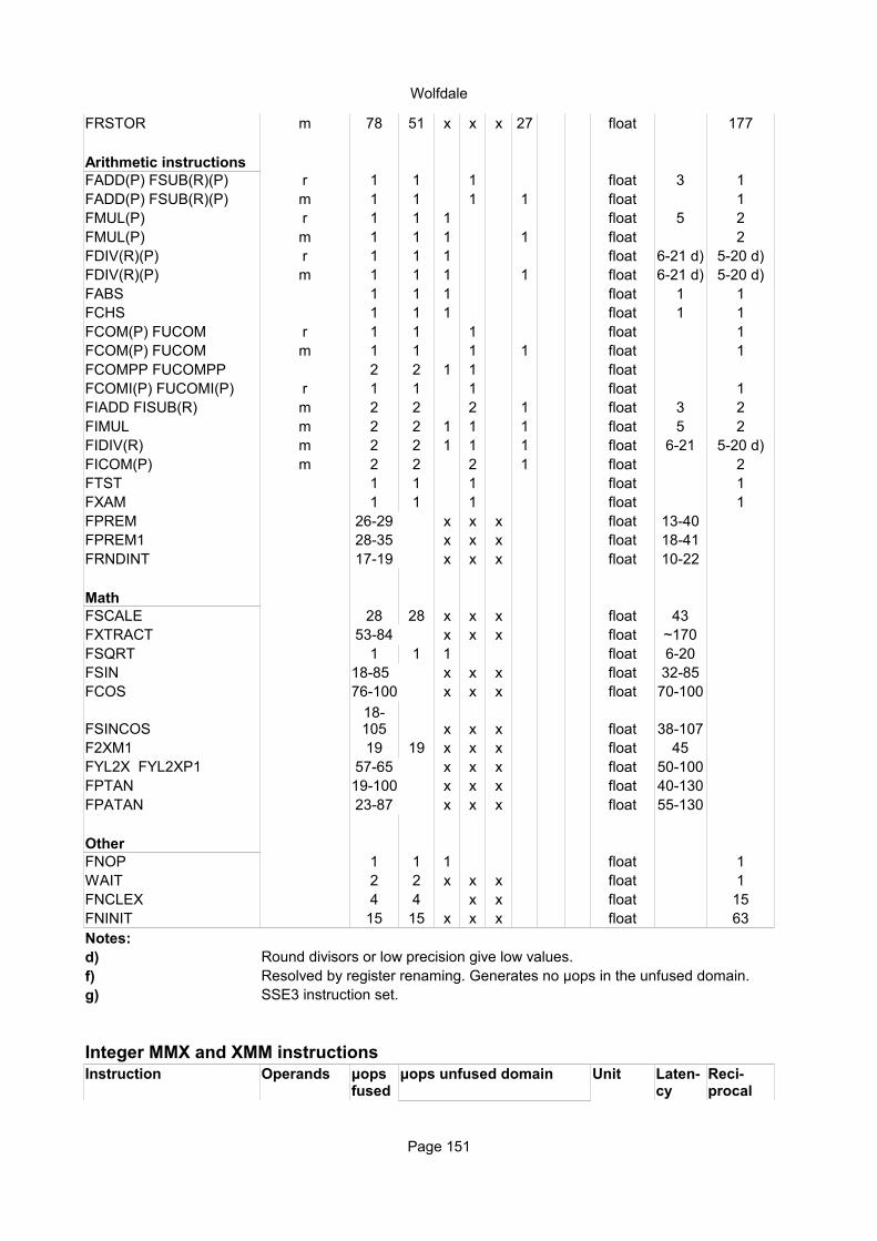
Wolfdale
Page 151
FRSTOR m 78 51 x x x 27 float 177
Arithmetic instructionsFADD(P) FSUB(R)(P) r 1 1 1 float 3 1FADD(P) FSUB(R)(P) m 1 1 1 1 float 1FMUL(P) r 1 1 1 float 5 2FMUL(P) m 1 1 1 1 float 2FDIV(R)(P) r 1 1 1 float 6-21 d) 5-20 d)FDIV(R)(P) m 1 1 1 1 float 6-21 d) 5-20 d)FABS 1 1 1 float 1 1FCHS 1 1 1 float 1 1FCOM(P) FUCOM r 1 1 1 float 1FCOM(P) FUCOM m 1 1 1 1 float 1FCOMPP FUCOMPP 2 2 1 1 floatFCOMI(P) FUCOMI(P) r 1 1 1 float 1FIADD FISUB(R) m 2 2 2 1 float 3 2FIMUL m 2 2 1 1 1 float 5 2FIDIV(R) m 2 2 1 1 1 float 6-21 5-20 d)FICOM(P) m 2 2 2 1 float 2FTST 1 1 1 float 1FXAM 1 1 1 float 1FPREM 26-29 x x x float 13-40FPREM1 28-35 x x x float 18-41FRNDINT 17-19 x x x float 10-22
MathFSCALE 28 28 x x x float 43FXTRACT 53-84 x x x float ~170FSQRT 1 1 1 float 6-20FSIN 18-85 x x x float 32-85FCOS 76-100 x x x float 70-100
FSINCOS x x x float 38-107F2XM1 19 19 x x x float 45
57-65 x x x float 50-100FPTAN 19-100 x x x float 40-130FPATAN 23-87 x x x float 55-130
OtherFNOP 1 1 1 float 1WAIT 2 2 x x x float 1FNCLEX 4 4 x x float 15FNINIT 15 15 x x x float 63Notes:d) Round divisors or low precision give low values.f) Resolved by register renaming. Generates no μops in the unfused domain.g) SSE3 instruction set.
Integer MMX and XMM instructionsInstruction Operands μops unfused domain Unit
18-105
FYL2X FYL2XP1
μops fused do-main
Laten-cy
Reci-procal through-put

Wolfdale
Page 152
p015 p0 p1 p5 p2 p3 p4
Move instructionsMOVD k) r,(x)mm 1 1 x x x int 2 0,33MOVD k) m,(x)mm 1 1 1 3 1MOVD k) (x)mm,r 1 1 x x int 2 0,5MOVD k) (x)mm,m 1 1 int 2 1MOVQ v,v 1 1 x x x int 1 0,33MOVQ (x)mm,m64 1 1 int 2 1MOVQ m64, (x)mm 1 1 1 3 1MOVDQA xmm, xmm 1 1 x x x int 1 0,33MOVDQA xmm, m128 1 1 int 2 1MOVDQA m128, xmm 1 1 1 3 1MOVDQU m128, xmm 9 4 x x x 1 2 2 3-8 4MOVDQU xmm, m128 4 2 x x 2 int 2-8 2LDDQU g) xmm, m128 4 2 x x 2 int 2-8 2MOVDQ2Q mm, xmm 1 1 x x x int 1 0,33MOVQ2DQ xmm,mm 1 1 x x x int 1 0,33MOVNTQ m64,mm 1 1 1 2MOVNTDQ m128,xmm 1 1 1 2MOVNTDQA j) xmm, m128 1 1 2 1
mm,mm 1 1 1 int 1 1
mm,m64 1 1 1 1 int 1
xmm,xmm 1 1 1 int 1 1
xmm,m128 1 1 1 1 int 1PACKUSDW j) xmm,xmm 1 1 1 int 1 1PACKUSDW j) xmm,m 1 1 1 1 int 1PUNPCKH/LBW/WD/DQ mm,mm 1 1 1 int 1 1PUNPCKH/LBW/WD/DQ mm,m64 1 1 1 1 int 1PUNPCKH/LBW/WD/DQ xmm,xmm 1 1 1 int 1 1PUNPCKH/LBW/WD/DQ xmm,m128 1 1 1 1 int 1PUNPCKH/LQDQ xmm,xmm 1 1 1 int 1 1PUNPCKH/LQDQ xmm, m128 2 1 1 1 int 1PMOVSX/ZXBW j) xmm,xmm 1 1 1 int 1 1PMOVSX/ZXBW j) xmm,m64 1 1 1 1 int 1PMOVSX/ZXBD j) xmm,xmm 1 1 1 int 1 1PMOVSX/ZXBD j) xmm,m32 1 1 1 1 int 1PMOVSX/ZXBQ j) xmm,xmm 1 1 1 int 1 1PMOVSX/ZXBQ j) xmm,m16 1 1 1 1 int 1PMOVSX/ZXWD j) xmm,xmm 1 1 1 int 1 1PMOVSX/ZXWD j) xmm,m64 1 1 1 1 int 1PMOVSX/ZXWQ j) xmm,xmm 1 1 1 int 1 1PMOVSX/ZXWQ j) xmm,m32 1 1 1 1 int 1PMOVSX/ZXDQ j) xmm,xmm 1 1 1 int 1 1PMOVSX/ZXDQ j) xmm,m64 1 1 1 1 int 1PSHUFB h) mm,mm 1 1 1 int 1 1PSHUFB h) mm,m64 2 1 1 1 int 1PSHUFB h) xmm,xmm 1 1 1 int 1 1PSHUFB h) xmm,m128 1 1 1 1 int 1
μops fused do-main
Reci-procal through-put
PACKSSWB/DW PACKUSWB
PACKSSWB/DW PACKUSWB
PACKSSWB/DW PACKUSWB
PACKSSWB/DW PACKUSWB
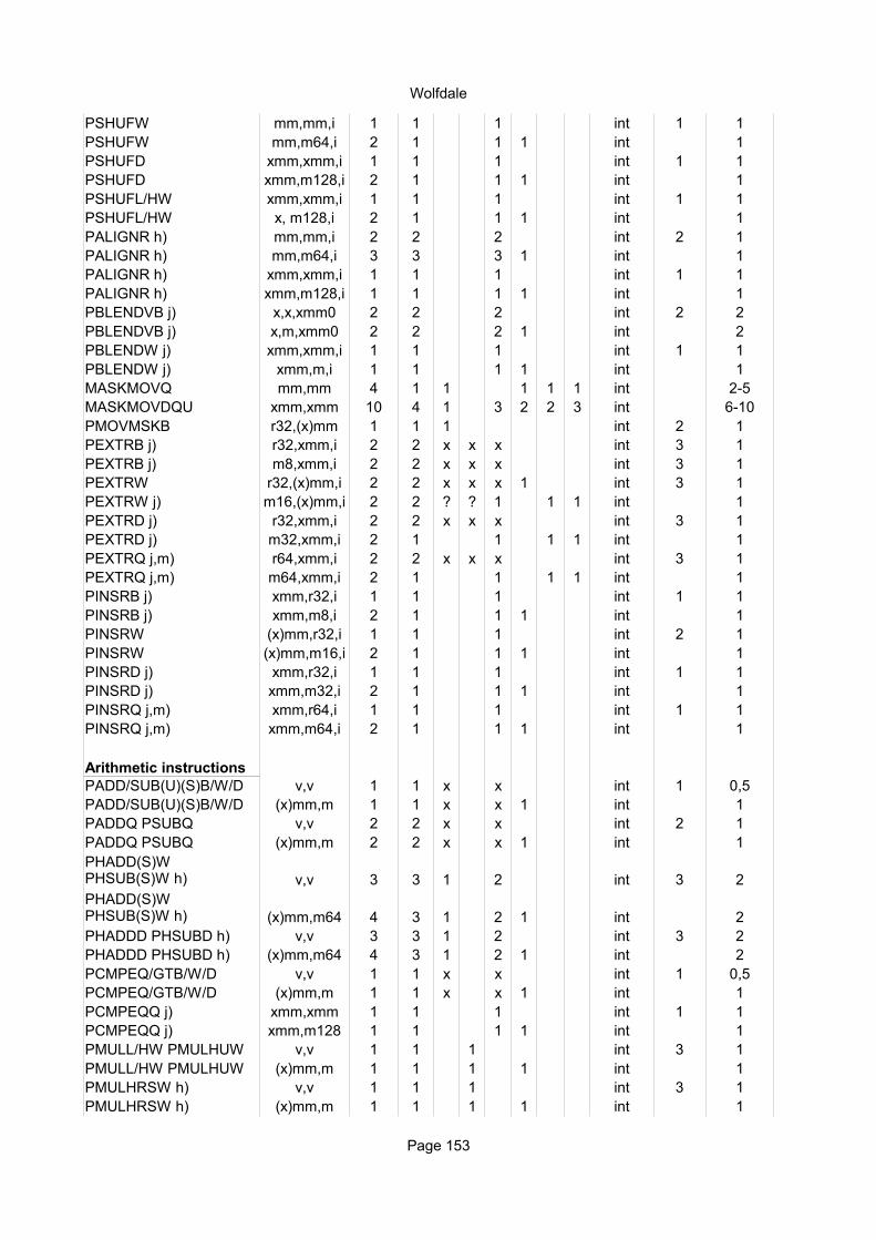
Wolfdale
Page 153
PSHUFW mm,mm,i 1 1 1 int 1 1PSHUFW mm,m64,i 2 1 1 1 int 1PSHUFD xmm,xmm,i 1 1 1 int 1 1PSHUFD xmm,m128,i 2 1 1 1 int 1PSHUFL/HW xmm,xmm,i 1 1 1 int 1 1PSHUFL/HW x, m128,i 2 1 1 1 int 1PALIGNR h) mm,mm,i 2 2 2 int 2 1PALIGNR h) mm,m64,i 3 3 3 1 int 1PALIGNR h) xmm,xmm,i 1 1 1 int 1 1PALIGNR h) xmm,m128,i 1 1 1 1 int 1PBLENDVB j) x,x,xmm0 2 2 2 int 2 2PBLENDVB j) x,m,xmm0 2 2 2 1 int 2PBLENDW j) xmm,xmm,i 1 1 1 int 1 1PBLENDW j) xmm,m,i 1 1 1 1 int 1MASKMOVQ mm,mm 4 1 1 1 1 1 int 2-5MASKMOVDQU xmm,xmm 10 4 1 3 2 2 3 int 6-10PMOVMSKB r32,(x)mm 1 1 1 int 2 1PEXTRB j) r32,xmm,i 2 2 x x x int 3 1PEXTRB j) m8,xmm,i 2 2 x x x int 3 1PEXTRW r32,(x)mm,i 2 2 x x x 1 int 3 1PEXTRW j) m16,(x)mm,i 2 2 ? ? 1 1 1 int 1PEXTRD j) r32,xmm,i 2 2 x x x int 3 1PEXTRD j) m32,xmm,i 2 1 1 1 1 int 1PEXTRQ j,m) r64,xmm,i 2 2 x x x int 3 1PEXTRQ j,m) m64,xmm,i 2 1 1 1 1 int 1PINSRB j) xmm,r32,i 1 1 1 int 1 1PINSRB j) xmm,m8,i 2 1 1 1 int 1PINSRW (x)mm,r32,i 1 1 1 int 2 1PINSRW (x)mm,m16,i 2 1 1 1 int 1PINSRD j) xmm,r32,i 1 1 1 int 1 1PINSRD j) xmm,m32,i 2 1 1 1 int 1PINSRQ j,m) xmm,r64,i 1 1 1 int 1 1PINSRQ j,m) xmm,m64,i 2 1 1 1 int 1
Arithmetic instructionsPADD/SUB(U)(S)B/W/D v,v 1 1 x x int 1 0,5PADD/SUB(U)(S)B/W/D (x)mm,m 1 1 x x 1 int 1PADDQ PSUBQ v,v 2 2 x x int 2 1PADDQ PSUBQ (x)mm,m 2 2 x x 1 int 1
v,v 3 3 1 2 int 3 2
(x)mm,m64 4 3 1 2 1 int 2PHADDD PHSUBD h) v,v 3 3 1 2 int 3 2PHADDD PHSUBD h) (x)mm,m64 4 3 1 2 1 int 2PCMPEQ/GTB/W/D v,v 1 1 x x int 1 0,5PCMPEQ/GTB/W/D (x)mm,m 1 1 x x 1 int 1PCMPEQQ j) xmm,xmm 1 1 1 int 1 1PCMPEQQ j) xmm,m128 1 1 1 1 int 1PMULL/HW PMULHUW v,v 1 1 1 int 3 1PMULL/HW PMULHUW (x)mm,m 1 1 1 1 int 1PMULHRSW h) v,v 1 1 1 int 3 1PMULHRSW h) (x)mm,m 1 1 1 1 int 1
PHADD(S)W PHSUB(S)W h)
PHADD(S)W PHSUB(S)W h)

Wolfdale
Page 154
PMULLD j) xmm,xmm 4 4 2 2 int 5 2PMULLD j) xmm,m128 6 5 1 2 2 1 int 5 4PMULDQ j) xmm,xmm 1 1 1 int 3 1PMULDQ j) xmm,m128 1 1 1 1 int 1PMULUDQ v,v 1 1 1 int 3 1PMULUDQ (x)mm,m 1 1 1 1 int 1PMADDWD v,v 1 1 1 int 3 1PMADDWD (x)mm,m 1 1 1 1 int 1PMADDUBSW h) v,v 1 1 1 int 3 1PMADDUBSW h) (x)mm,m 1 1 1 1 int 1PAVGB/W v,v 1 1 x x int 1 0,5PAVGB/W (x)mm,m 1 1 x x 1 int 1PMIN/MAXSB j) xmm,xmm 1 1 1 int 1 1PMIN/MAXSB j) xmm,m128 1 1 1 1 int 1PMIN/MAXUB v,v 1 1 x x int 1 0,5PMIN/MAXUB (x)mm,m 1 1 x x 1 int 1PMIN/MAXSW v,v 1 1 x x int 1 0,5PMIN/MAXSW (x)mm,m 1 1 x x 1 int 1PMIN/MAXUW j) xmm,xmm 1 1 1 int 1 1PMIN/MAXUW j) xmm,m 1 1 1 int 1PMIN/MAXSD j) xmm,xmm 1 1 1 int 1 1PMIN/MAXSD j) xmm,m128 1 1 1 1 int 1PMIN/MAXUD j) xmm,xmm 1 1 1 int 1 1PMIN/MAXUD j) xmm,m128 1 1 1 1 int 1PHMINPOSUW j) xmm,xmm 4 4 4 int 4 4PHMINPOSUW j) xmm,m128 4 4 4 1 int 4PABSB PABSW PABSD h) v,v 1 1 x x int 1 0,5
(x)mm,m 1 1 x x 1 int 1
v,v 1 1 x x int 1 0,5
(x)mm,m 1 1 x x 1 int 1PSADBW v,v 1 1 1 int 3 1PSADBW (x)mm,m 1 1 1 1 int 1MPSADBW j) xmm,xmm,i 3 3 1 2 int 5 2MPSADBW j) xmm,m,i 4 3 1 2 1 int 2
Logic instructionsPAND(N) POR PXOR v,v 1 1 x x x int 1 0,33PAND(N) POR PXOR (x)mm,m 1 1 x x x 1 int 1PTEST j) xmm,xmm 2 2 1 x x int 1 1PTEST j) xmm,m128 2 2 1 x x 1 int 1PSLL/RL/RAW/D/Q mm,mm/i 1 1 1 int 1 1PSLL/RL/RAW/D/Q mm,m64 1 1 1 1 int 1PSLL/RL/RAW/D/Q xmm,i 1 1 1 int 1 1PSLL/RL/RAW/D/Q xmm,xmm 2 2 x x int 2 1PSLL/RL/RAW/D/Q xmm,m128 3 2 x x 1 int 1PSLL/RLDQ xmm,i 1 1 x x int 1 1
OtherEMMS 11 11 x x x float 6Notes:
PABSB PABSW PABSD h)
PSIGNB PSIGNW PSIGND h)
PSIGNB PSIGNW PSIGND h)

Wolfdale
Page 155
g) SSE3 instruction set.h) Supplementary SSE3 instruction set.j) SSE4.1 instruction setk)
m) Only available in 64 bit mode
Floating point XMM instructionsInstruction Operands μops unfused domain Unit
p015 p0 p1 p5 p2 p3 p4Move instructionsMOVAPS/D xmm,xmm 1 1 x x x int 1 0,33MOVAPS/D xmm,m128 1 1 int 2 1MOVAPS/D m128,xmm 1 1 1 3 1MOVUPS/D xmm,m128 4 2 1 1 2 int 2-4 2MOVUPS/D m128,xmm 9 4 x x x 1 2 2 3-4 4MOVSS/D xmm,xmm 1 1 x x x int 1 0,33MOVSS/D x,m32/64 1 1 int 2 1MOVSS/D m32/64,x 1 1 1 3 1MOVHPS/D MOVLPS/D xmm,m64 2 1 1 1 int 3 1MOVHPS/D m64,xmm 2 1 1 1 1 5 1MOVLPS/D m64,xmm 1 1 1 3 1MOVLHPS MOVHLPS xmm,xmm 1 1 1 float 1 1MOVMSKPS/D r32,xmm 1 1 1 float 1 1MOVNTPS/D m128,xmm 1 1 1 2-3SHUFPS xmm,xmm,i 1 1 1 int 1 1SHUFPS xmm,m128,i 2 1 1 1 int 1SHUFPD xmm,xmm,i 1 1 1 float 1 1SHUFPD xmm,m128,i 2 1 1 1 float 1BLENDPS/PD j) xmm,xmm,i 1 1 1 int 1 1BLENDPS/PD j) xmm,m128,i 1 1 1 1 int 1BLENDVPS/PD j) x,x,xmm0 2 2 2 int 2 2BLENDVPS/PD j) x,m,xmm0 2 2 2 1 int 2MOVDDUP g) xmm,xmm 1 1 1 int 1 1MOVDDUP g) xmm,m64 2 1 1 1 int 1MOVSH/LDUP g) xmm,xmm 1 1 1 int 1 1MOVSH/LDUP g) xmm,m128 2 1 1 1 int 1UNPCKH/LPS xmm,xmm 1 1 1 int 1 1UNPCKH/LPS xmm,m128 1 1 1 1 int 1UNPCKH/LPD xmm,xmm 1 1 1 float 1 1UNPCKH/LPD xmm,m128 2 1 1 1 float 1EXTRACTPS j) r32,xmm,i 2 2 x x x int 4 1EXTRACTPS j) m32,xmm,i 2 1 1 1 1 int 1INSERTPS j) xmm,xmm,i 1 1 1 int 1 1INSERTPS j) xmm,m32,i 2 1 1 1 int 1
ConversionCVTPD2PS xmm,xmm 2 2 1 1 float 4 1CVTPD2PS xmm,m128 2 2 1 1 1 float 1CVTSD2SS xmm,xmm 2 2 1 1 float 4 1CVTSD2SS xmm,m64 2 2 1 1 1 float 1
MASM uses the name MOVD rather than MOVQ for this instruction even when moving 64 bits
μops fused do-main
Laten-cy
Reci-procal through-put

Wolfdale
Page 156
CVTPS2PD xmm,xmm 2 2 2 float 2 2CVTPS2PD xmm,m64 2 2 2 1 float 2CVTSS2SD xmm,xmm 2 2 2 float 2 2CVTSS2SD xmm,m32 2 2 2 1 float 2CVTDQ2PS xmm,xmm 1 1 1 float 3 1CVTDQ2PS xmm,m128 1 1 1 1 float 1CVT(T) PS2DQ xmm,xmm 1 1 1 float 3 1CVT(T) PS2DQ xmm,m128 1 1 1 1 float 1CVTDQ2PD xmm,xmm 2 2 1 1 float 4 1CVTDQ2PD xmm,m64 2 2 1 1 1 float 1CVT(T)PD2DQ xmm,xmm 2 2 1 1 float 4 1CVT(T)PD2DQ xmm,m128 2 2 1 1 1 float 1CVTPI2PS xmm,mm 1 1 1 float 3 3CVTPI2PS xmm,m64 1 1 1 1 float 3CVT(T)PS2PI mm,xmm 1 1 1 float 3 1CVT(T)PS2PI mm,m128 1 1 1 1 float 1CVTPI2PD xmm,mm 2 2 1 1 float 4 1CVTPI2PD xmm,m64 2 2 1 1 1 float 1CVT(T) PD2PI mm,xmm 2 2 1 1 float 4 1CVT(T) PD2PI mm,m128 2 2 1 1 1 float 1CVTSI2SS xmm,r32 1 1 1 float 4 3CVTSI2SS xmm,m32 1 1 1 1 float 3CVT(T)SS2SI r32,xmm 1 1 1 float 3 1CVT(T)SS2SI r32,m32 1 1 1 1 float 1CVTSI2SD xmm,r32 2 2 1 1 float 4 3CVTSI2SD xmm,m32 2 1 1 1 float 3CVT(T)SD2SI r32,xmm 1 1 1 float 3 1CVT(T)SD2SI r32,m64 1 1 1 1 float 1
ArithmeticADDSS/D SUBSS/D xmm,xmm 1 1 1 float 3 1ADDSS/D SUBSS/D x,m32/64 1 1 1 1 float 1ADDPS/D SUBPS/D xmm,xmm 1 1 1 float 3 1ADDPS/D SUBPS/D xmm,m128 1 1 1 1 float 1ADDSUBPS/D g) xmm,xmm 1 1 1 float 3 1ADDSUBPS/D g) xmm,m128 1 1 1 1 float 1HADDPS HSUBPS g) xmm,xmm 3 3 1 2 float 7 3HADDPS HSUBPS g) xmm,m128 4 3 1 2 1 float 3HADDPD HSUBPD g) xmm,xmm 3 3 x x x float 6 1,5HADDPD HSUBPD g) xmm,m128 4 3 x x x 1 float 1,5MULSS xmm,xmm 1 1 1 float 4 1MULSS xmm,m32 1 1 1 1 float 1MULSD xmm,xmm 1 1 1 float 5 1MULSD xmm,m64 1 1 1 1 float 1MULPS xmm,xmm 1 1 1 float 4 1MULPS xmm,m128 1 1 1 1 float 1MULPD xmm,xmm 1 1 1 float 5 1MULPD xmm,m128 1 1 1 1 float 1DIVSS xmm,xmm 1 1 1 float 6-13 d) 5-12 d)DIVSS xmm,m32 1 1 1 1 float 5-12 d)DIVSD xmm,xmm 1 1 1 float 6-21 d) 5-20 d)DIVSD xmm,m64 1 1 1 1 float 5-20 d)DIVPS xmm,xmm 1 1 1 float 6-13 d) 5-12 d)

Wolfdale
Page 157
DIVPS xmm,m128 1 1 1 1 float 5-12 d)DIVPD xmm,xmm 1 1 1 float 6-21 d) 5-20 d)DIVPD xmm,m128 1 1 1 1 float 5-20 d)RCPSS/PS xmm,xmm 1 1 1 float 3 2RCPSS/PS xmm,m 1 1 1 1 float 2CMPccSS/D xmm,xmm 1 1 1 float 3 1CMPccSS/D x,m32/64 1 1 1 1 float 1CMPccPS/D xmm,xmm 1 1 1 float 3 1CMPccPS/D xmm,m128 1 1 1 1 float 1COMISS/D UCOMISS/D xmm,xmm 1 1 1 float 3 1COMISS/D UCOMISS/D x,m32/64 1 1 1 1 float 1MAXSS/D MINSS/D xmm,xmm 1 1 1 float 3 1MAXSS/D MINSS/D x,m32/64 1 1 1 1 float 1MAXPS/D MINPS/D xmm,xmm 1 1 1 float 3 1MAXPS/D MINPS/D xmm,m128 1 1 1 1 float 1ROUNDSS/D j) xmm,xmm,i 1 1 1 float 3 1ROUNDSS/D j) xmm,m128,i 1 1 1 1 float 1ROUNDPS/D j) xmm,xmm,i 1 1 1 float 3 1ROUNDPS/D j) xmm,m128,i 1 1 1 1 float 1DPPS j) xmm,xmm,i 4 4 2 2 float 11 3DPPS j) xmm,m128,i 4 4 2 2 1 float 3DPPD j) xmm,xmm,i 4 4 x x x float 9 3DPPD j) xmm,m128,i 4 4 x x x 1 float 3
MathSQRTSS/PS xmm,xmm 1 1 1 float 6-13 5-12SQRTSS/PS xmm,m 2 1 1 1 float 5-12SQRTSD/PD xmm,xmm 1 1 1 float 6-20 5-19SQRTSD/PD xmm,m 2 1 1 1 float 5-19RSQRTSS/PS xmm,xmm 1 1 1 float 3 2RSQRTSS/PS xmm,m 1 1 1 1 float 2
LogicAND/ANDN/OR/XORPS/D xmm,xmm 1 1 x x x int 1 0,33AND/ANDN/OR/XORPS/D xmm,m128 1 1 x x x 1 int 1
OtherLDMXCSR m32 13 12 x x x 1 38STMXCSR m32 10 8 x x x 1 1 20FXSAVE m4096 151 67 x x x 8 38 38 145FXRSTOR m4096 121 74 x x x 47 150Notes:d) Round divisors give low values.g) SSE3 instruction set.

Nehalem
Page 158
Intel NehalemList of instruction timings and μop breakdown
Explanation of column headings:Operands:
μops fused domain:
μops unfused domain:
p015: The total number of μops going to port 0, 1 and 5.p0: The number of μops going to port 0 (execution units).p1: The number of μops going to port 1 (execution units). p5: The number of μops going to port 5 (execution units). p2: The number of μops going to port 2 (memory read).p3: The number of μops going to port 3 (memory write address).p4: The number of μops going to port 4 (memory write data).Domain:
i = immediate data, r = register, mm = 64 bit mmx register, xmm = 128 bit xmm register, (x)mm = mmx or xmm register, sr = segment register, m = memory, m32 = 32-bit memory operand, etc.
The number of μops at the decode, rename, allocate and retirement stages in the pipeline. Fused μops count as one.
The number of μops for each execution port. Fused μops count as two. Fused macro-ops count as one. The instruction has μop fusion if the sum of the num-bers listed under p015 + p2 + p3 + p4 exceeds the number listed under μops fused domain. An x under p0, p1 or p5 means that at least one of the μops listed under p015 can optionally go to this port. For example, a 1 under p015 and an x under p0 and p5 means one μop which can go to either port 0 or port 5, whichever is vacant first. A value listed under p015 but nothing under p0, p1 and p5 means that it is not known which of the three ports these μops go to.
Tells which execution unit domain is used: "int" = integer unit (general purpose registers), "ivec" = integer vector unit (SIMD), "fp" = floating point unit (XMM and x87 floating point). An additional "bypass delay" is generated if a register written by a μop in one domain is read by a μop in another domain. The by-pass delay is 1 clock cycle between the "int" and "ivec" units, and 2 clock cy-cles between the "int" and "fp", and between the "ivec" and "fp" units.
The bypass delay is indicated under latency only where it is unavoidable be-cause either the source operand or the destination operand is in an unnatural domain such as a general purpose register (e.g. eax) in the "ivec" domain. For example, the PEXTRW instruction executes in the "int" domain. The source operand is an xmm register and the destination operand is a general purpose register. The latency for this instruction is indicated as 2+1, where 2 is the la-tency of the instruction itself and 1 is the bypass delay, assuming that the xmm operand is most likely to come from the "ivec" domain. If the xmm operand comes from the "fp" domain then the bypass delay will be 2 rather than one. The flags register can also have a bypass delay. For example, the COMISS in-struction (floating point compare) executes in the "fp" domain and returns the result in the integer flags. Almost all instructions that read these flags execute in the "int" domain. Here the latency is indicated as 1+2, where 1 is the latency of the instruction itself and 2 is the bypass delay from the "fp" domain to the "int" domain.
The bypass delay from the memory read unit to any other unit and from any unit to the memory write unit are included in the latency figures in the table. Where the domain is not listed, the bypass delays are either unlikely to occur or unavoidable and therefore included in the latency figure.
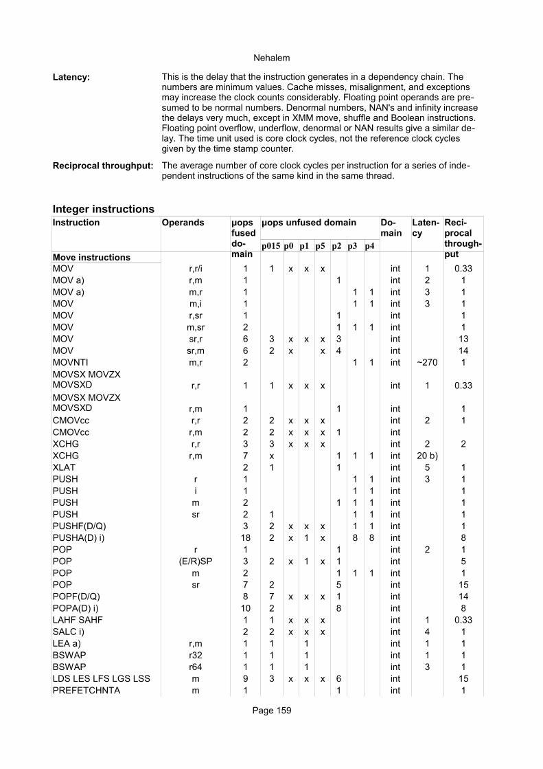
Nehalem
Page 159
Latency:
Reciprocal throughput:
Integer instructionsInstruction Operands μops unfused domain
p015 p0 p1 p5 p2 p3 p4Move instructionsMOV r,r/i 1 1 x x x int 1 0.33MOV a) r,m 1 1 int 2 1MOV a) m,r 1 1 1 int 3 1MOV m,i 1 1 1 int 3 1MOV r,sr 1 1 int 1MOV m,sr 2 1 1 1 int 1MOV sr,r 6 3 x x x 3 int 13MOV sr,m 6 2 x x 4 int 14MOVNTI m,r 2 1 1 int ~270 1
r,r 1 1 x x x int 1 0.33
r,m 1 1 int 1CMOVcc r,r 2 2 x x x int 2 1CMOVcc r,m 2 2 x x x 1 intXCHG r,r 3 3 x x x int 2 2XCHG r,m 7 x 1 1 1 int 20 b)XLAT 2 1 1 int 5 1PUSH r 1 1 1 int 3 1PUSH i 1 1 1 int 1PUSH m 2 1 1 1 int 1PUSH sr 2 1 1 1 int 1PUSHF(D/Q) 3 2 x x x 1 1 int 1PUSHA(D) i) 18 2 x 1 x 8 8 int 8POP r 1 1 int 2 1POP (E/R)SP 3 2 x 1 x 1 int 5POP m 2 1 1 1 int 1POP sr 7 2 5 int 15POPF(D/Q) 8 7 x x x 1 int 14POPA(D) i) 10 2 8 int 8LAHF SAHF 1 1 x x x int 1 0.33SALC i) 2 2 x x x int 4 1LEA a) r,m 1 1 1 int 1 1BSWAP r32 1 1 1 int 1 1BSWAP r64 1 1 1 int 3 1LDS LES LFS LGS LSS m 9 3 x x x 6 int 15PREFETCHNTA m 1 1 int 1
This is the delay that the instruction generates in a dependency chain. The numbers are minimum values. Cache misses, misalignment, and exceptions may increase the clock counts considerably. Floating point operands are pre-sumed to be normal numbers. Denormal numbers, NAN's and infinity increase the delays very much, except in XMM move, shuffle and Boolean instructions. Floating point overflow, underflow, denormal or NAN results give a similar de-lay. The time unit used is core clock cycles, not the reference clock cycles given by the time stamp counter.
The average number of core clock cycles per instruction for a series of inde-pendent instructions of the same kind in the same thread.
μops fused do-main
Do-main
Laten-cy
Reci-procal through-put
MOVSX MOVZX MOVSXD
MOVSX MOVZX MOVSXD

Nehalem
Page 160
PREFETCHT0/1/2 m 1 1 int 1LFENCE 2 1 1 int 9MFENCE 3 1 x x x 1 1 int 23SFENCE 2 1 1 int 5
Arithmetic instructionsADD SUB r,r/i 1 1 x x x int 1 0.33ADD SUB r,m 1 1 x x x 1 int 1ADD SUB m,r/i 2 1 x x x 1 1 1 int 6 1ADC SBB r,r/i 2 2 x x x int 2 2ADC SBB r,m 2 2 x x x 1 int 2 2ADC SBB m,r/i 4 3 x x x 1 1 1 int 7CMP r,r/i 1 1 x x x int 1 0.33CMP m,r/i 1 1 x x x 1 int 1 1INC DEC NEG NOT r 1 1 x x x int 1 0.33INC DEC NEG NOT m 3 1 x x x 1 1 1 int 6 1AAA AAS DAA DAS i) 1 1 1 int 3 1AAD i) 3 3 x x x int 15 2AAM i) 5 5 x x x int 20 7MUL IMUL r8 1 1 1 int 3 1MUL IMUL r16 3 3 x x x int 5 2MUL IMUL r32 3 3 x x x int 5 2MUL IMUL r64 3 3 x x x int 3 2IMUL r16,r16 1 1 1 int 3 1IMUL r32,r32 1 1 1 int 3 1IMUL r64,r64 1 1 1 int 3 1IMUL r16,r16,i 1 1 1 int 3 1IMUL r32,r32,i 1 1 1 int 3 1IMUL r64,r64,i 1 1 1 int 3 2MUL IMUL m8 1 1 1 1 int 3 1MUL IMUL m16 3 3 x x x 1 int 5 2MUL IMUL m32 3 3 x x x 1 int 5 2MUL IMUL m64 3 2 2 1 int 3 2IMUL r16,m16 1 1 1 1 int 3 1IMUL r32,m32 1 1 1 1 int 3 1IMUL r64,m64 1 1 1 1 int 3 1IMUL r16,m16,i 1 1 1 1 int 1IMUL r32,m32,i 1 1 1 1 int 1IMUL r64,m64,i 1 1 1 1 int 1DIV c) r8 4 4 1 2 1 int 11-21 7-11DIV c) r16 6 6 x 4 x int 17-22 7-12DIV c) r32 6 6 x 3 x int 17-28 7-17DIV c) r64 ~40 x x x x int 28-90 19-69IDIV c) r8 4 4 1 2 1 int 10-22 7-11IDIV c) r16 8 8 x 5 x int 18-23 7-12IDIV c) r32 7 7 x 3 x int 17-28 7-17IDIV c) r64 ~60 x x x x int 37-100 26-86CBW CWDE CDQE 1 1 x x x int 1 1CWD CDQ CQO 1 1 x x int 1 1POPCNT ℓ) r,r 1 1 1 int 3 1POPCNT ℓ) r,m 1 1 1 1 int 1CRC32 ℓ) r,r 1 1 1 int 3 1CRC32 ℓ) r,m 1 1 1 1 int 1

Nehalem
Page 161
Logic instructionsAND OR XOR r,r/i 1 1 x x x int 1 0.33AND OR XOR r,m 1 1 x x x 1 int 1AND OR XOR m,r/i 2 1 x x x 1 1 1 int 6 1TEST r,r/i 1 1 x x x int 1 0.33TEST m,r/i 1 1 x x x 1 int 1SHR SHL SAR r,i/cl 1 1 x x int 1 0.5SHR SHL SAR m,i/cl 3 2 x x 1 1 1 int 6 1ROR ROL r,i/cl 1 1 x x int 1 1ROR ROL m,i/cl 3 2 x x 1 1 1 int 6 1RCR RCL r,1 2 2 x x x int 2 2RCR r8,i/cl 9 9 x x x int 13RCL r8,i/cl 8 8 x x x int 11RCR RCL r16/32/64,i/cl 6 6 x x x int 12-13 12-13RCR RCL m,1 4 3 x x x 1 1 1 int 7RCR m8,i/cl 12 9 x x x 1 1 1 int 16RCL m8,i/cl 11 8 x x x 1 1 1 int 14RCR RCL m16/32/64,i/cl 10 7 x x x 1 1 1 int 15SHLD r,r,i/cl 2 2 x x x int 3 1SHLD m,r,i/cl 3 2 x x x 1 1 1 int 8SHRD r,r,i/cl 2 2 x x x int 4 1SHRD m,r,i/cl 3 2 x x x 1 1 1 int 9BT r,r/i 1 1 x x int 1 1BT m,r 9 8 x x 1 int 5BT m,i 2 2 x x 1 int 1BTR BTS BTC r,r/i 1 1 x x int 1 1BTR BTS BTC m,r 10 7 x x x 1 1 1 int 6BTR BTS BTC m,i 3 3 x x 1 1 1 int 6BSF BSR r,r 1 1 1 int 3 1BSF BSR r,m 2 1 1 1 int 3 1SETcc r 1 1 x x int 1 1SETcc m 2 1 x x x 1 1 int 1CLC STC CMC 1 1 x x x int 1 0.33CLD 2 2 x x x int 4STD 2 2 x x x int 5
Control transfer instructionsJMP short/near 1 1 1 int 0 2JMP i) far 31 31 int 67JMP r 1 1 1 int 0 2JMP m(near) 1 1 1 1 int 0 2JMP m(far) 31 31 11 int 73Conditional jump short/near 1 1 1 int 0 2Fused compare/test and branch e) 1 1 1 int 0 2J(E/R)CXZ short 2 2 x x 1 int 2LOOP short 6 6 x x x int 4LOOP(N)E short 11 11 x x x int 7CALL near 2 2 ? ? 1 1 1 int 2CALL i) far 46 46 9 int 74CALL r 3 2 ? ? 1 1 1 int 2CALL m(near) 4 3 ? ? 1 1 1 1 int 2CALL m(far) 47 47 1 int 79

Nehalem
Page 162
RETN 1 1 1 1 int 2RETN i 3 2 1 1 int 2RETF 39 39 int 120RETF i 40 40 int 124BOUND i) r,m 15 13 2 int 7INTO i) 4 4 int 5
String instructionsLODS 2 1 x x x 1 int 1REP LODS 11+4n int 40+12nSTOS 3 1 x x x 1 1 int 1REP STOS small n 60+n int 12+nREP STOS large n 2.5/16 bytes int 1 clk / 16 bytesMOVS 5 2 x x x 1 1 1 int 4REP MOVS small n 13+6n int 12+nREP MOVS large n 2/16 bytes int 1 clk / 16 bytesSCAS 3 2 x x x 1 int 1REP SCAS 37+6n int 40+2nCMPS 5 3 x x x 2 int 4REP CMPS 65+8n int 42+2n
OtherNOP (90) 1 1 x x x int 0.33Long NOP (0F 1F) 1 1 x x x int 1PAUSE 5 5 x x x int 9ENTER a,0 11 9 x x x 1 1 1 int 8ENTER a,b 34+7b int 79+5bLEAVE 3 3 1 int 5CPUID 25-100 int ~200 ~200RDTSC 22 int 24RDPMC 28 int 40-60Notes:a) Applies to all addressing modesb) Has an implicit LOCK prefix. c) Low values are for small results, high values for high results.e)
i) Not available in 64 bit mode.ℓ) SSE4.2 instruction set.
Floating point x87 instructionsInstruction Operands μops unfused domain
p015 p0 p1 p5 p2 p3 p4Move instructionsFLD r 1 1 1 float 1 1FLD m32/64 1 1 1 float 3 1FLD m80 4 2 1 1 2 float 4 2FBLD m80 41 38 x x x 3 float 45 20FST(P) r 1 1 1 float 1 1FST(P) m32/m64 1 1 1 float 4 1
See manual 3: "The microarchitecture of Intel, AMD and VIA CPUs" for restric-tions on macro-op fusion.
μops fused do-main
Do-main
Laten-cy
Reci-procal through-put

Nehalem
Page 163
FSTP m80 7 3 x x x 2 2 float 5 5FBSTP m80 208 204 x x x 2 2 float 242 245FXCH r 1 0 f) float 0 1FILD m 1 1 1 1 float 6 1FIST(P) m 3 1 1 1 1 float 7 1FISTTP g) m 3 1 1 1 1 float 7 1FLDZ 1 1 1 float 1FLD1 2 2 1 1 float 2FLDPI FLDL2E etc. 2 2 2 float 2FCMOVcc r 2 2 2 float 2+2 2FNSTSW AX 2 2 float 1FNSTSW m16 3 2 1 1 float 2FLDCW m16 2 1 1 float 7 31FNSTCW m16 2 1 1 1 1 float 5 1FINCSTP FDECSTP 1 1 1 float 1 1FFREE(P) r 2 2 x x x float 4FNSAVE m 143 89 x x x 8 23 23 float 178 178FRSTOR m 79 52 x x x 27 float 156 156
Arithmetic instructionsFADD(P) FSUB(R)(P) r 1 1 1 float 3 1FADD(P) FSUB(R)(P) m 1 1 1 1 float 1FMUL(P) r 1 1 1 float 5 1FMUL(P) m 1 1 1 1 float 1FDIV(R)(P) r 1 1 1 float 7-27 d) 7-27 d)FDIV(R)(P) m 1 1 1 1 float 7-27 d) 7-27 d)FABS 1 1 1 float 1 1FCHS 1 1 1 float 1 1FCOM(P) FUCOM r 1 1 1 float 1FCOM(P) FUCOM m 1 1 1 1 float 1FCOMPP FUCOMPP 2 2 1 1 float 1FCOMI(P) FUCOMI(P) r 1 1 1 float 1FIADD FISUB(R) m 2 2 2 1 float 3 2FIMUL m 2 2 1 1 1 float 5 2FIDIV(R) m 2 2 1 1 1 float 7-27 d) 7-27 d)FICOM(P) m 2 2 2 1 float 1FTST 1 1 1 float 1FXAM 1 1 1 float 1FPREM 25 25 x x x float 14FPREM1 35 35 x x x float 19FRNDINT 17 17 x x x float 22
MathFSCALE 24 24 x x x float 12FXTRACT 17 17 x x x float 13FSQRT 1 1 1 float ~27FSIN ~100 ~100 x x x float 40-100FCOS ~100 ~100 x x x float 40-100FSINCOS ~100 ~100 x x x float ~110F2XM1 19 19 x x x float 58FYL2X FYL2XP1 ~55 ~55 x x x float ~80FPTAN ~100 ~100 x x x float ~115FPATAN ~82 ~82 x x x float ~120

Nehalem
Page 164
OtherFNOP 1 1 1 float 1WAIT 2 2 x x x float 1FNCLEX 3 3 x x float 17FNINIT ~190 ~190 x x x float 77Notes:d) Round divisors or low precision give low values.f) Resolved by register renaming. Generates no μops in the unfused domain.g) SSE3 instruction set.
Integer MMX and XMM instructionsInstruction Operands μops unfused domain
p015 p0 p1 p5 p2 p3 p4Move instructionsMOVD k) r32/64,(x)mm 1 1 x x x int 1+1 0.33MOVD k) m32/64,(x)mm 1 1 1 3 1MOVD k) (x)mm,r32/64 1 1 x x x ivec 1+1 0.33MOVD k) (x)mm,m32/64 1 1 2 1MOVQ (x)mm, (x)mm 1 1 x x x ivec 1 0.33MOVQ (x)mm,m64 1 1 2 1MOVQ m64, (x)mm 1 1 1 3 1MOVDQA xmm, xmm 1 1 x x x ivec 1 0.33MOVDQA xmm, m128 1 1 2 1MOVDQA m128, xmm 1 1 1 3 1MOVDQU xmm, m128 1 1 1 2 1MOVDQU m128, xmm 1 1 1 1 3 1LDDQU g) xmm, m128 1 1 1 2 1MOVDQ2Q mm, xmm 1 1 x x x ivec 1 0.33MOVQ2DQ xmm,mm 1 1 x x x ivec 1 0.33MOVNTQ m64,mm 1 1 1 ~270 2MOVNTDQ m128,xmm 1 1 1 ~270 2MOVNTDQA j) xmm, m128 1 1 2 1
mm,mm 1 1 1 ivec 1 1
mm,m64 1 1 1 1 2
xmm,xmm 1 1 x x ivec 1 0.5
xmm,m128 1 1 x x 1 2PACKUSDW j) xmm,xmm 1 1 x x ivec 1 2PACKUSDW j) xmm,m 1 1 x x 1 2PUNPCKH/LBW/WD/DQ (x)mm, (x)mm 1 1 x x ivec 1 0.5PUNPCKH/LBW/WD/DQ (x)mm,m 1 1 x x 1 2PUNPCKH/LQDQ xmm,xmm 1 1 x x ivec 1 0.5PUNPCKH/LQDQ xmm, m128 2 1 x x 1 1PMOVSX/ZXBW j) xmm,xmm 1 1 x x ivec 1 1PMOVSX/ZXBW j) xmm,m64 1 1 x x 1 2PMOVSX/ZXBD j) xmm,xmm 1 1 x x ivec 1 1PMOVSX/ZXBD j) xmm,m32 1 1 x x 1 2
μops fused do-main
Do-main
Laten-cy
Reci-procal through-put
PACKSSWB/DW PACKUSWB
PACKSSWB/DW PACKUSWB
PACKSSWB/DW PACKUSWB
PACKSSWB/DW PACKUSWB
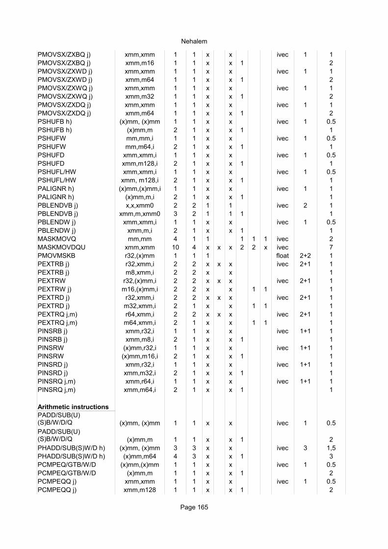
Nehalem
Page 165
PMOVSX/ZXBQ j) xmm,xmm 1 1 x x ivec 1 1PMOVSX/ZXBQ j) xmm,m16 1 1 x x 1 2PMOVSX/ZXWD j) xmm,xmm 1 1 x x ivec 1 1PMOVSX/ZXWD j) xmm,m64 1 1 x x 1 2PMOVSX/ZXWQ j) xmm,xmm 1 1 x x ivec 1 1PMOVSX/ZXWQ j) xmm,m32 1 1 x x 1 2PMOVSX/ZXDQ j) xmm,xmm 1 1 x x ivec 1 1PMOVSX/ZXDQ j) xmm,m64 1 1 x x 1 2PSHUFB h) (x)mm, (x)mm 1 1 x x ivec 1 0.5PSHUFB h) (x)mm,m 2 1 x x 1 1PSHUFW mm,mm,i 1 1 x x ivec 1 0.5PSHUFW mm,m64,i 2 1 x x 1 1PSHUFD xmm,xmm,i 1 1 x x ivec 1 0.5PSHUFD xmm,m128,i 2 1 x x 1 1PSHUFL/HW xmm,xmm,i 1 1 x x ivec 1 0.5PSHUFL/HW xmm, m128,i 2 1 x x 1 1PALIGNR h) (x)mm,(x)mm,i 1 1 x x ivec 1 1PALIGNR h) (x)mm,m,i 2 1 x x 1 1PBLENDVB j) x,x,xmm0 2 2 1 1 ivec 2 1PBLENDVB j) xmm,m,xmm0 3 2 1 1 1 1PBLENDW j) xmm,xmm,i 1 1 x x ivec 1 0.5PBLENDW j) xmm,m,i 2 1 x x 1 1MASKMOVQ mm,mm 4 1 1 1 1 1 ivec 2MASKMOVDQU xmm,xmm 10 4 x x x 2 2 x ivec 7PMOVMSKB r32,(x)mm 1 1 1 float 2+2 1PEXTRB j) r32,xmm,i 2 2 x x x ivec 2+1 1PEXTRB j) m8,xmm,i 2 2 x x 1PEXTRW r32,(x)mm,i 2 2 x x x ivec 2+1 1PEXTRW j) m16,(x)mm,i 2 2 x x 1 1 1PEXTRD j) r32,xmm,i 2 2 x x x ivec 2+1 1PEXTRD j) m32,xmm,i 2 1 x x 1 1 1PEXTRQ j,m) r64,xmm,i 2 2 x x x ivec 2+1 1PEXTRQ j,m) m64,xmm,i 2 1 x x 1 1 1PINSRB j) xmm,r32,i 1 1 x x ivec 1+1 1PINSRB j) xmm,m8,i 2 1 x x 1 1PINSRW (x)mm,r32,i 1 1 x x ivec 1+1 1PINSRW (x)mm,m16,i 2 1 x x 1 1PINSRD j) xmm,r32,i 1 1 x x ivec 1+1 1PINSRD j) xmm,m32,i 2 1 x x 1 1PINSRQ j,m) xmm,r64,i 1 1 x x ivec 1+1 1PINSRQ j,m) xmm,m64,i 2 1 x x 1 1
Arithmetic instructions
(x)mm, (x)mm 1 1 x x ivec 1 0.5
(x)mm,m 1 1 x x 1 2PHADD/SUB(S)W/D h) (x)mm, (x)mm 3 3 x x ivec 3 1,5PHADD/SUB(S)W/D h) (x)mm,m64 4 3 x x 1 3PCMPEQ/GTB/W/D (x)mm,(x)mm 1 1 x x ivec 1 0.5PCMPEQ/GTB/W/D (x)mm,m 1 1 x x 1 2PCMPEQQ j) xmm,xmm 1 1 x x ivec 1 0.5PCMPEQQ j) xmm,m128 1 1 x x 1 2
PADD/SUB(U)(S)B/W/D/Q
PADD/SUB(U)(S)B/W/D/Q
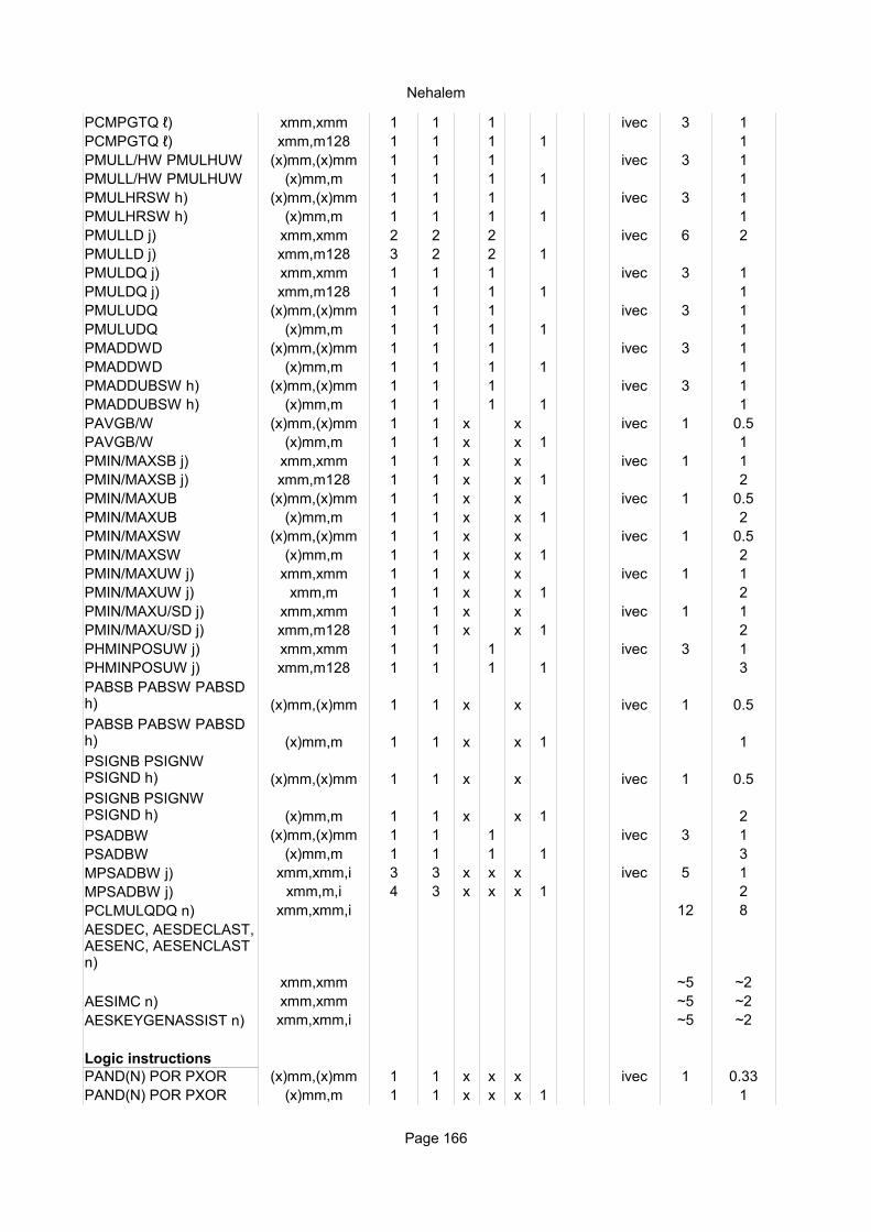
Nehalem
Page 166
PCMPGTQ ℓ) xmm,xmm 1 1 1 ivec 3 1PCMPGTQ ℓ) xmm,m128 1 1 1 1 1PMULL/HW PMULHUW (x)mm,(x)mm 1 1 1 ivec 3 1PMULL/HW PMULHUW (x)mm,m 1 1 1 1 1PMULHRSW h) (x)mm,(x)mm 1 1 1 ivec 3 1PMULHRSW h) (x)mm,m 1 1 1 1 1PMULLD j) xmm,xmm 2 2 2 ivec 6 2PMULLD j) xmm,m128 3 2 2 1PMULDQ j) xmm,xmm 1 1 1 ivec 3 1PMULDQ j) xmm,m128 1 1 1 1 1PMULUDQ (x)mm,(x)mm 1 1 1 ivec 3 1PMULUDQ (x)mm,m 1 1 1 1 1PMADDWD (x)mm,(x)mm 1 1 1 ivec 3 1PMADDWD (x)mm,m 1 1 1 1 1PMADDUBSW h) (x)mm,(x)mm 1 1 1 ivec 3 1PMADDUBSW h) (x)mm,m 1 1 1 1 1PAVGB/W (x)mm,(x)mm 1 1 x x ivec 1 0.5PAVGB/W (x)mm,m 1 1 x x 1 1PMIN/MAXSB j) xmm,xmm 1 1 x x ivec 1 1PMIN/MAXSB j) xmm,m128 1 1 x x 1 2PMIN/MAXUB (x)mm,(x)mm 1 1 x x ivec 1 0.5PMIN/MAXUB (x)mm,m 1 1 x x 1 2PMIN/MAXSW (x)mm,(x)mm 1 1 x x ivec 1 0.5PMIN/MAXSW (x)mm,m 1 1 x x 1 2PMIN/MAXUW j) xmm,xmm 1 1 x x ivec 1 1PMIN/MAXUW j) xmm,m 1 1 x x 1 2PMIN/MAXU/SD j) xmm,xmm 1 1 x x ivec 1 1PMIN/MAXU/SD j) xmm,m128 1 1 x x 1 2PHMINPOSUW j) xmm,xmm 1 1 1 ivec 3 1PHMINPOSUW j) xmm,m128 1 1 1 1 3
(x)mm,(x)mm 1 1 x x ivec 1 0.5
(x)mm,m 1 1 x x 1 1
(x)mm,(x)mm 1 1 x x ivec 1 0.5
(x)mm,m 1 1 x x 1 2PSADBW (x)mm,(x)mm 1 1 1 ivec 3 1PSADBW (x)mm,m 1 1 1 1 3MPSADBW j) xmm,xmm,i 3 3 x x x ivec 5 1MPSADBW j) xmm,m,i 4 3 x x x 1 2PCLMULQDQ n) xmm,xmm,i 12 8
xmm,xmm ~5 ~2AESIMC n) xmm,xmm ~5 ~2AESKEYGENASSIST n) xmm,xmm,i ~5 ~2
Logic instructionsPAND(N) POR PXOR (x)mm,(x)mm 1 1 x x x ivec 1 0.33PAND(N) POR PXOR (x)mm,m 1 1 x x x 1 1
PABSB PABSW PABSD h)
PABSB PABSW PABSD h)
PSIGNB PSIGNW PSIGND h)
PSIGNB PSIGNW PSIGND h)
AESDEC, AESDECLAST, AESENC, AESENCLAST n)

Nehalem
Page 167
PTEST j) xmm,xmm 2 2 x x x ivec 3 1PTEST j) xmm,m128 2 2 x x x 1 1PSLL/RL/RAW/D/Q mm,mm/i 1 1 1 ivec 1 1PSLL/RL/RAW/D/Q mm,m64 1 1 1 1 2PSLL/RL/RAW/D/Q xmm,i 1 1 1 ivec 1 1PSLL/RL/RAW/D/Q xmm,xmm 2 2 x 1 x ivec 2 2PSLL/RL/RAW/D/Q xmm,m128 3 2 x 1 x 1 1PSLL/RLDQ xmm,i 1 1 x x ivec 1 1
String instructionsPCMPESTRI ℓ) xmm,xmm,i 8 8 x x x ivec 14 5PCMPESTRI ℓ) xmm,m128,i 9 8 x x x 1 ivec 14 6PCMPESTRM ℓ) xmm,xmm,i 9 9 x x x ivec 7 6PCMPESTRM ℓ) xmm,m128,i 10 10 x x x 1 ivec 7 6PCMPISTRI ℓ) xmm,xmm,i 3 3 x x x ivec 8 2PCMPISTRI ℓ) xmm,m128,i 4 4 x x x 1 ivec 8 2PCMPISTRM ℓ) xmm,xmm,i 4 4 x x x ivec 7 2PCMPISTRM ℓ) xmm,m128,i 6 5 x x x 1 ivec 7 5
OtherEMMS 11 11 x x x float 6Notes:g) SSE3 instruction set.h) Supplementary SSE3 instruction set.j) SSE4.1 instruction setk)
ℓ) SSE4.2 instruction setm) Only available in 64 bit moden) Only available on newer models
Floating point XMM instructionsInstruction Operands μops unfused domain
p015 p0 p1 p5 p2 p3 p4Move instructionsMOVAPS/D xmm,xmm 1 1 1 float 1 1MOVAPS/D xmm,m128 1 1 2 1MOVAPS/D m128,xmm 1 1 1 3 1MOVUPS/D xmm,m128 1 1 2 1-4MOVUPS/D m128,xmm 1 1 1 3 1-3MOVSS/D xmm,xmm 1 1 1 1 1MOVSS/D xmm,m32/64 1 1 2 1MOVSS/D m32/64,xmm 1 1 1 3 1MOVHPS/D MOVLPS/D xmm,m64 2 1 1 1 3 2MOVH/LPS/D m64,xmm 2 1 1 1 1 5 1MOVLHPS MOVHLPS xmm,xmm 1 1 1 float 1 1MOVMSKPS/D r32,xmm 1 1 1 float 1+2 1MOVNTPS/D m128,xmm 1 1 1 ~270 2SHUFPS/D xmm,xmm,i 1 1 1 float 1 1SHUFPS/D xmm,m128,i 2 1 1 1 float 1BLENDPS/PD j) xmm,xmm,i 1 1 1 float 1 1
MASM uses the name MOVD rather than MOVQ for this instruction even when moving 64 bits
μops fused do-main
Do-main
Laten-cy
Reci-procal through-put

Nehalem
Page 168
BLENDPS/PD j) xmm,m128,i 2 1 1 1 float 1BLENDVPS/PD j) x,x,xmm0 2 2 2 float 2 2BLENDVPS/PD j) xmm,m,xmm0 3 2 2 1 float 2MOVDDUP g) xmm,xmm 1 1 1 float 1 1MOVDDUP g) xmm,m64 1 1 2 1MOVSH/LDUP g) xmm,xmm 1 1 1 float 1 1MOVSH/LDUP g) xmm,m128 1 1 1UNPCKH/LPS/D xmm,xmm 1 1 1 float 1 1UNPCKH/LPS/D xmm,m128 1 1 1 1 float 1EXTRACTPS j) r32,xmm,i 1 1 1 float 1+2 1EXTRACTPS j) m32,xmm,i 2 1 1 1 1 1INSERTPS j) xmm,xmm,i 1 1 1 float 1 1INSERTPS j) xmm,m32,i 3 2 2 1 float 2
ConversionCVTPD2PS xmm,xmm 2 2 1 1 float 4 1CVTPD2PS xmm,m128 2 2 1 1 float 1CVTSD2SS xmm,xmm 2 2 1 1 float 4 1CVTSD2SS xmm,m64 2 2 ? ? ? 1 float 1CVTPS2PD xmm,xmm 2 2 1 1 float 2 1CVTPS2PD xmm,m64 2 2 1 1 1 float 1CVTSS2SD xmm,xmm 1 1 1 float 1 1CVTSS2SD xmm,m32 1 1 1 1 float 2CVTDQ2PS xmm,xmm 1 1 1 float 3+2 1CVTDQ2PS xmm,m128 1 1 1 1 float 1CVT(T) PS2DQ xmm,xmm 1 1 1 float 3+2 1CVT(T) PS2DQ xmm,m128 1 1 1 1 float 1CVTDQ2PD xmm,xmm 2 2 1 1 float 4+2 1CVTDQ2PD xmm,m64 2 2 1 1 1 float 1CVT(T)PD2DQ xmm,xmm 2 2 1 1 float 4+2 1CVT(T)PD2DQ xmm,m128 2 2 1 1 1 float 1CVTPI2PS xmm,mm 1 1 1 float 3+2 3CVTPI2PS xmm,m64 1 1 1 1 float 3CVT(T)PS2PI mm,xmm 1 1 1 float 3+2 1CVT(T)PS2PI mm,m128 1 1 1 1 float 1CVTPI2PD xmm,mm 2 2 1 1 ivec/float 6 1CVTPI2PD xmm,m64 2 2 1 1 1 1CVT(T) PD2PI mm,xmm 2 2 x 1 x float/ivec 6 1CVT(T) PD2PI mm,m128 2 2 x 1 x 1 1CVTSI2SS xmm,r32 1 1 1 float 3+2 3CVTSI2SS xmm,m32 1 1 1 1 float 3CVT(T)SS2SI r32,xmm 1 1 1 float 3+2 1CVT(T)SS2SI r32,m32 1 1 1 1 float 1CVTSI2SD xmm,r32 2 2 1 1 float 4+2 3CVTSI2SD xmm,m32 2 1 1 1 float 3CVT(T)SD2SI r32,xmm 1 1 1 float 3+2 1CVT(T)SD2SI r32,m64 1 1 1 1 float 1
ArithmeticADDSS/D SUBSS/D xmm,xmm 1 1 1 float 3 1ADDSS/D SUBSS/D xmm,m32/64 1 1 1 1 float 1ADDPS/D SUBPS/D xmm,xmm 1 1 1 float 3 1ADDPS/D SUBPS/D xmm,m128 1 1 1 1 float 1

Nehalem
Page 169
ADDSUBPS/D g) xmm,xmm 1 1 1 float 3 1ADDSUBPS/D g) xmm,m128 1 1 1 1 float 1HADDPS HSUBPS g) xmm,xmm 3 3 1 2 float 5 2HADDPS HSUBPS g) xmm,m128 4 3 1 2 1 float 2HADDPD HSUBPD g) xmm,xmm 3 3 1 2 float 3 2HADDPD HSUBPD g) xmm,m128 4 3 1 2 1 float 2MULSS MULPS xmm,xmm 1 1 1 float 4 1MULSS MULPS xmm,m 1 1 1 1 float 1MULSD MULPD xmm,xmm 1 1 1 float 5 1MULSD MULPD xmm,m 1 1 1 1 float 1DIVSS DIVPS xmm,xmm 1 1 1 float 7-14 7-14DIVSS DIVPS xmm,m 1 1 1 1 float 7-14DIVSD DIVPD xmm,xmm 1 1 1 float 7-22 7-22DIVSD DIVPD xmm,m 1 1 1 1 float 7-22RCPSS/PS xmm,xmm 1 1 1 float 3 2RCPSS/PS xmm,m 1 1 1 1 float 2CMPccSS/D CMPccPS/D
xmm,xmm 1 1 1 float 3 1CMPccSS/D CMPccPS/D
xmm,m 2 1 1 1 float 1COMISS/D UCOMISS/D xmm,xmm 1 1 1 float 1+2 1COMISS/D UCOMISS/D xmm,m32/64 1 1 1 1 float 1MAXSS/D MINSS/D xmm,xmm 1 1 1 float 3 1MAXSS/D MINSS/D xmm,m32/64 1 1 1 1 float 1MAXPS/D MINPS/D xmm,xmm 1 1 1 float 3 1MAXPS/D MINPS/D xmm,m128 1 1 1 1 float 1
xmm,xmm,i 1 1 1 float 3 1
xmm,m128,i 2 1 1 1 float 1DPPS j) xmm,xmm,i 4 4 1 2 1 float 11 2DPPS j) xmm,m128,i 6 5 x x x 1 floatDPPD j) xmm,xmm,i 3 3 x x x float 9 1DPPD j) xmm,m128,i 4 3 x x x 1 float 3
MathSQRTSS/PS xmm,xmm 1 1 1 float 7-18 7-18SQRTSS/PS xmm,m 2 1 1 1 float 7-18SQRTSD/PD xmm,xmm 1 1 1 float 7-32 7-32SQRTSD/PD xmm,m 2 1 1 1 float 7-32RSQRTSS/PS xmm,xmm 1 1 1 float 3 2RSQRTSS/PS xmm,m 1 1 1 1 float 2
LogicAND/ANDN/OR/XORPS/D xmm,xmm 1 1 1 float 1 1AND/ANDN/OR/XORPS/D xmm,m128 1 1 1 1 float 1
OtherLDMXCSR m32 6 6 x x x 1 5STMXCSR m32 2 1 1 1 1 1FXSAVE m4096 141 141 x x x 5 38 38 90 90FXRSTOR m4096 112 90 x x x 42 100Notes:
ROUNDSS/D ROUNDPS/D j)
ROUNDSS/D ROUNDPS/D j)

Nehalem
Page 170
g) SSE3 instruction set.

Sandy Bridge
Page 171
Intel Sandy BridgeList of instruction timings and μop breakdown
Explanation of column headings:Operands:
μops fused domain:
μops unfused domain:
p015: The total number of μops going to port 0, 1 and 5.p0: The number of μops going to port 0 (execution units).p1: The number of μops going to port 1 (execution units). p5: The number of μops going to port 5 (execution units). p23: The number of μops going to port 2 or 3 (memory read or address calculation).p4: The number of μops going to port 4 (memory write data).Latency:
Reciprocal throughput:
Integer instructionsInstruction Operands μops unfused domain Latency
p015 p0 p1 p5 p23 p4
Move instructionsMOV r,r/i 1 1 x x x 1
i = immediate data, r = register, mm = 64 bit mmx register, x = 128 bit xmm reg-ister, (x)mm = mmx or xmm register, y = 256 bit ymm register, same = same register for both operands. m = memory operand, m32 = 32-bit memory oper-and, etc.
The number of μops at the decode, rename, allocate and retirement stages in the pipeline. Fused μops count as one.
The number of μops for each execution port. Fused μops count as two. Fused macro-ops count as one. The instruction has μop fusion if the sum of the num-bers listed under p015 + p23 + p4 exceeds the number listed under μops fused domain. A number indicated as 1+ under a read or write port means a 256-bit read or write operation using two clock cycles for handling 128 bits each cycle. The port cannot receive another read or write µop in the second clock cycle, but a read port can receive an address-calculation µop in the second clock cycle. An x under p0, p1 or p5 means that at least one of the μops listed under p015 can optionally go to this port. For example, a 1 under p015 and an x under p0 and p5 means one μop which can go to either port 0 or port 5, whichever is va-cant first. A value listed under p015 but nothing under p0, p1 and p5 means that it is not known which of the three ports these μops go to.
This is the delay that the instruction generates in a dependency chain. The numbers are minimum values. Cache misses, misalignment, and exceptions may increase the clock counts considerably. Where hyperthreading is enabled, the use of the same execution units in the other thread leads to inferior perfor-mance. Denormal numbers, NAN's and infinity do not increase the latency. The time unit used is core clock cycles, not the reference clock cycles given by the time stamp counter.
The average number of core clock cycles per instruction for a series of inde-pendent instructions of the same kind in the same thread.
The latencies and throughputs listed below for addition and multiplication using full size YMM registers are obtained only after a warm-up period of a thousand instructions or more. The latencies may be one or two clock cycles longer and the reciprocal throughputs double the values for shorter sequences of code. There is no warm-up effect when vectors are 128 bits wide or less.
μops fused do-main
Reci-procal through-put
Com-ments

Sandy Bridge
Page 172
MOV r,m 1 1 2 0.5
MOV m,r 1 1 1 3 1MOV m,i 1 1 1 1MOVNTI m,r 2 1 1 ~350 1
r,r 1 1 x x x 1
r,m 1 1 0.5
CMOVcc r,r 2 2 x x x 2 1CMOVcc r,m 2 2 x x x 1 1XCHG r,r 3 3 x x x 2 1XCHG r,m 8 x 2 1 25
XLAT 3 2 1 7 1PUSH r 1 1 1 3 1PUSH i 1 1 1 1PUSH m 2 2 1 1PUSHF(D/Q) 3 2 x x x 1 1 1PUSHA(D) 16 0 8 8 8 not 64 bitPOP r 1 1 2 0.5POP (E/R)SP 1 0 1 0.5POP m 2 2 1 1POPF(D/Q) 9 8 x x x 1 18POPA(D) 18 10 8 9 not 64 bitLAHF SAHF 1 1 1 1SALC 3 3 1 1 not 64 bitLEA r,m 1 1 x x 1 0.5 simpleLEA r,m 1 1 1 3 1
BSWAP r32 1 1 1 1 1BSWAP r64 2 2 2 2 1PREFETCHNTA m 1 1 0.5PREFETCHT0/1/2 m 1 1 0.5LFENCE 2 1 1 4MFENCE 3 1 1 1 33SFENCE 2 1 1 6
Arithmetic instructionsADD SUB r,r/i 1 1 x x x 1ADD SUB r,m 1 1 x x x 1 0.5ADD SUB m,r/i 2 1 x x x 2 1 6 1SUB r,same 1 0 0 0.25ADC SBB r,r/i 2 2 x x x 2 1ADC SBB r,m 2 2 x x x 1 2 1ADC SBB m,r/i 4 3 x x x 2 1 7 1,5CMP r,r/i 1 1 x x x 1CMP m,r/i 1 1 x x x 1 1 0.5INC DEC NEG NOT r 1 1 x x x 1INC DEC NEG NOT m 3 1 x x x 2 1 6 2
all ad-dressing modes
MOVSX MOVZX MOVSXD
MOVSX MOVZX MOVSXD
implicit lock
complex or rip rel-
ative

Sandy Bridge
Page 173
AAA AAS 2 2 4 not 64 bit
DAA DAS 3 3 4 not 64 bitAAD 3 3 2 not 64 bitAAM 8 8 20 11 not 64 bitMUL IMUL r8 1 1 1 3 1MUL IMUL r16 4 4 4 2MUL IMUL r32 3 3 4 2MUL IMUL r64 2 2 3 1IMUL r,r 1 1 1 3 1IMUL r16,r16,i 2 2 4 1IMUL r32,r32,i 1 1 1 3 1IMUL r64,r64,i 1 1 1 3 1MUL IMUL m8 1 1 1 1 3 1MUL IMUL m16 4 3 1 2MUL IMUL m32 3 2 1 2MUL IMUL m64 2 1 1 2IMUL r,m 1 1 1 1 1IMUL r16,m16,i 2 2 1 1IMUL r32,m32,i 1 1 1 1 1IMUL r64,m64,i 1 1 1 1 1DIV r8 10 10 20-24 11-14DIV r16 11 11 21-25 11-14DIV r32 10 10 20-28 11-18DIV r64 34-56 x 30-94 22-76IDIV r8 10 10 21-24 11-14IDIV r16 10 10 21-25 11-14IDIV r32 9 9 20-27 11-18IDIV r64 x 40-103 25-84
CBW 1 1 1 0.5CWDE 1 1 1 1 1CDQE 1 1 1 0.5CWD 2 2 1 1CDQ 1 1 1 1CQO 1 1 1 0.5POPCNT r,r 1 1 1 3 1 SSE4.2POPCNT r,m 1 1 1 1 1 SSE4.2CRC32 r,r 1 1 1 3 1 SSE4.2CRC32 r,m 1 1 1 1 1 SSE4.2
Logic instructionsAND OR XOR r,r/i 1 1 x x x 1AND OR XOR r,m 1 1 x x x 1 0.5AND OR XOR m,r/i 2 1 x x x 2 1 6 1XOR r,same 1 0 0 0.25TEST r,r/i 1 1 x x x 1TEST m,r/i 1 1 x x x 1 0.5SHR SHL SAR r,i 1 1 x x 1 0.5SHR SHL SAR m,i 3 1 2 1 2SHR SHL SAR r,cl 3 3 2 2SHR SHL SAR m,cl 5 3 2 1 4ROR ROL r,i 1 1 1 1
59-138
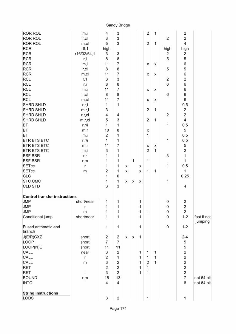
Sandy Bridge
Page 174
ROR ROL m,i 4 3 2 1 2ROR ROL r,cl 3 3 2 2ROR ROL m,cl 5 3 2 1 4RCR r8,1 high high highRCR r16/32/64,1 3 3 2 2RCR r,i 8 8 5 5RCR m,i 11 7 x x 6RCR r,cl 8 8 5 5RCR m,cl 11 7 x x 6RCL r,1 3 3 2 2RCL r,i 8 8 6 6RCL m,i 11 7 x x 6RCL r,cl 8 8 6 6RCL m,cl 11 7 x x 6SHRD SHLD r,r,i 1 1 0.5SHRD SHLD m,r,i 3 2 1 2SHRD SHLD r,r,cl 4 4 2 2SHRD SHLD m,r,cl 5 3 2 1 4BT r,r/i 1 1 1 0.5BT m,r 10 8 x 5BT m,i 2 1 1 0.5BTR BTS BTC r,r/i 1 1 1 0.5BTR BTS BTC m,r 11 7 x x 5BTR BTS BTC m,i 3 1 2 1 2BSF BSR r,r 1 1 3 1BSF BSR r,m 1 1 1 1 1SETcc r 1 1 x x 1 0.5SETcc m 2 1 x x 1 1 1CLC 1 0 0.25STC CMC 1 1 x x x 1CLD STD 3 3 4
Control transfer instructionsJMP short/near 1 1 1 0 2JMP r 1 1 1 0 2JMP m 1 1 1 1 0 2Conditional jump short/near 1 1 1 0 1-2
1 1 1 0 1-2
J(E/R)CXZ short 2 2 x x 1 2-4LOOP short 7 7 5LOOP(N)E short 11 11 5CALL near 3 2 1 1 1 2CALL r 2 1 1 1 1 2CALL m 3 2 1 2 1 2RET 2 2 1 1 2RET i 3 2 1 1 2BOUND r,m 15 13 7 not 64 bitINTO 4 4 6 not 64 bit
String instructionsLODS 3 2 1 1
fast if not jumping
Fused arithmetic and branch
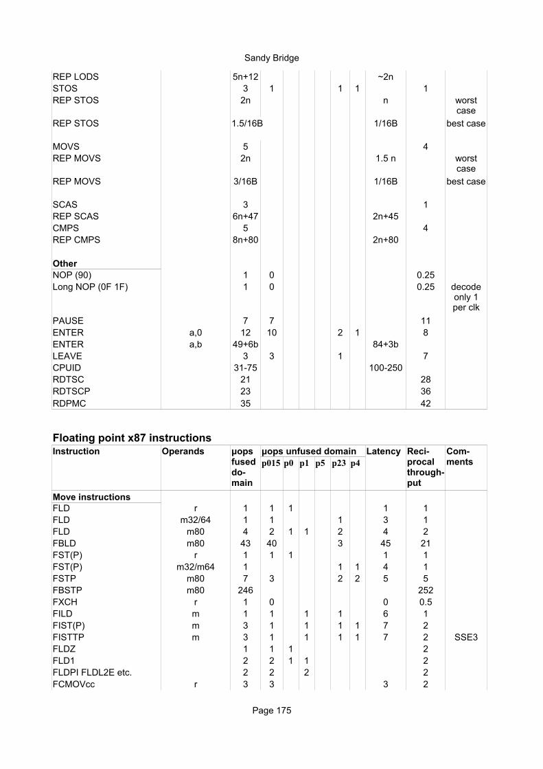
Sandy Bridge
Page 175
REP LODS 5n+12 ~2nSTOS 3 1 1 1 1REP STOS 2n n
REP STOS 1.5/16B 1/16B best case
MOVS 5 4REP MOVS 2n 1.5 n
REP MOVS 3/16B 1/16B best case
SCAS 3 1REP SCAS 6n+47 2n+45CMPS 5 4REP CMPS 8n+80 2n+80
OtherNOP (90) 1 0 0.25Long NOP (0F 1F) 1 0 0.25
PAUSE 7 7 11ENTER a,0 12 10 2 1 8ENTER a,b 49+6b 84+3bLEAVE 3 3 1 7CPUID 31-75 100-250RDTSC 21 28RDTSCP 23 36RDPMC 35 42
Floating point x87 instructionsInstruction Operands μops unfused domain Latency
p015 p0 p1 p5 p23 p4
Move instructionsFLD r 1 1 1 1 1FLD m32/64 1 1 1 3 1FLD m80 4 2 1 1 2 4 2FBLD m80 43 40 3 45 21FST(P) r 1 1 1 1 1FST(P) m32/m64 1 1 1 4 1FSTP m80 7 3 2 2 5 5FBSTP m80 246 252FXCH r 1 0 0 0.5FILD m 1 1 1 1 6 1FIST(P) m 3 1 1 1 1 7 2FISTTP m 3 1 1 1 1 7 2 SSE3FLDZ 1 1 1 2FLD1 2 2 1 1 2FLDPI FLDL2E etc. 2 2 2 2FCMOVcc r 3 3 3 2
worst case
worst case
decode only 1 per clk
μops fused do-main
Reci-procal through-put
Com-ments

Sandy Bridge
Page 176
FNSTSW AX 2 2 2 1FNSTSW m16 2 1 1 1 1FLDCW m16 3 2 1 8FNSTCW m16 2 1 1 1 1 5 1FINCSTP FDECSTP 1 1 1 1 1FFREE(P) r 1 1 1FNSAVE m 143 166FRSTOR m 90 165
Arithmetic instructionsFADD(P) FSUB(R)(P) r 1 1 1 3 1FADD(P) FSUB(R)(P) m 2 2 1 1 1FMUL(P) r 1 1 1 5 1FMUL(P) m 1 1 1 1 1FDIV(R)(P) r 1 1 1 10-24 10-24FDIV(R)(P) m 1 1 1 1 10-24FABS 1 1 1 1 1FCHS 1 1 1 1 1FCOM(P) FUCOM r 1 1 1 3 1FCOM(P) FUCOM m 1 1 1 1 1FCOMPP FUCOMPP 2 2 1 1 1FCOMI(P) FUCOMI(P) r 3 3 1 1 1 4 1FIADD FISUB(R) m 2 2 1 1FIMUL m 2 2 1 1 1 1FIDIV(R) m 2 2 1 1 1FICOM(P) m 2 2 2 1 2FTST 1 1 1 1FXAM 2 2 1 2FPREM 28 28 21 21FPREM1 41-87 26-50 26-50FRNDINT 17 17 22
MathFSCALE 27 27 12FXTRACT 17 17 10FSQRT 1 1 1 10-24FSIN 64-100 x 47-100FCOS 20-110 x 47-115FSINCOS 20-110 x 43-123F2XM1 53-118 x 61-69FYL2X FYL2XP1FPTAN 102 102 130FPATAN 28-91 x 93-146
OtherFNOP 1 1 1 1WAIT 2 2 1FNCLEX 5 5 22FNINIT 26 26 81
Integer MMX and XMM instructions

Sandy Bridge
Page 177
Instruction Operands μops unfused domain Latencyp015 p0 p1 p5 p23 p4
Move instructionsMOVD r32/64,(x)mm 1 1 x x x 1MOVD m32/64,(x)mm 1 1 1 3 1MOVD (x)mm,r32/64 1 1 x x x 1MOVD (x)mm,m32/64 1 1 3 0.5MOVQ (x)mm,(x)mm 1 1 x x x 1MOVQ (x)mm,m64 1 1 3 0.5MOVQ m64, (x)mm 1 1 1 3 1MOVDQA x,x 1 1 x x x 1MOVDQA x, m128 1 1 3 0.5MOVDQA m128, x 1 1 1 3 1MOVDQU x, m128 1 1 1 3 0.5MOVDQU m128, x 1 1 1 1 3 1LDDQU x, m128 1 1 1 3 0.5 SSE3MOVDQ2Q mm, x 2 2 1 1MOVQ2DQ x,mm 1 1 1MOVNTQ m64,mm 1 1 1 ~300 1MOVNTDQ m128,x 1 1 1 ~300MOVNTDQA x, m128 1 1 0.5 SSE4.1
mm,mm 1 1 1 1 1
mm,m64 1 1 1 1
x,x 1 1 x x 1 0.5
x,m128 1 1 x x 1 0.5PACKUSDW x,x 1 1 x x 1 0.5 SSE4.1PACKUSDW x,m 1 1 x x 1 0.5 SSE4.1PUNPCKH/LBW/WD/DQ (x)mm,(x)mm 1 1 x x 1 0.5PUNPCKH/LBW/WD/DQ (x)mm,m 1 1 x x 1 0.5PUNPCKH/LQDQ x,x 1 1 x x 1 0.5PUNPCKH/LQDQ x, m128 2 1 x x 1 0.5PMOVSX/ZXBW x,x 1 1 x x 1 0.5 SSE4.1PMOVSX/ZXBW x,m64 1 1 x x 1 0.5 SSE4.1PMOVSX/ZXBD x,x 1 1 x x 1 0.5 SSE4.1PMOVSX/ZXBD x,m32 1 1 x x 1 0.5 SSE4.1PMOVSX/ZXBQ x,x 1 1 x x 1 0.5 SSE4.1PMOVSX/ZXBQ x,m16 1 1 x x 1 0.5 SSE4.1PMOVSX/ZXWD x,x 1 1 x x 1 0.5 SSE4.1PMOVSX/ZXWD x,m64 1 1 x x 1 0.5 SSE4.1PMOVSX/ZXWQ x,x 1 1 x x 1 0.5 SSE4.1PMOVSX/ZXWQ x,m32 1 1 x x 1 0.5 SSE4.1PMOVSX/ZXDQ x,x 1 1 x x 1 0.5 SSE4.1PMOVSX/ZXDQ x,m64 1 1 x x 1 0.5 SSE4.1PSHUFB (x)mm,(x)mm 1 1 x x 1 0.5 SSSE3PSHUFB (x)mm,m 2 1 x x 1 0.5 SSSE3PSHUFW mm,mm,i 1 1 x x 1 0.5PSHUFW mm,m64,i 2 1 x x 1 0.5
μops fused do-main
Reci-procal through-put
Com-ments
PACKSSWB/DW PACKUSWB
PACKSSWB/DW PACKUSWBPACKSSWB/DW PACKUSWBPACKSSWB/DW PACKUSWB

Sandy Bridge
Page 178
PSHUFD x,x,i 1 1 x x 1 0.5PSHUFD x,m128,i 2 1 x x 1 0.5PSHUFL/HW x,x,i 1 1 x x 1 0.5PSHUFL/HW x, m128,i 2 1 x x 1 0.5PALIGNR (x)mm,(x)mm,i 1 1 x x 1 0.5 SSSE3PALIGNR (x)mm,m,i 2 1 x x 1 0.5 SSSE3PBLENDVB x,x,xmm0 2 2 1 1 2 1 SSE4.1PBLENDVB x,m,xmm0 3 2 1 1 1 1 SSE4.1PBLENDW x,x,i 1 1 x x 1 0.5 SSE4.1PBLENDW x,m,i 2 1 x x 1 0.5 SSE4.1MASKMOVQ mm,mm 4 1 1 2 1 1MASKMOVDQU x,x 10 4 4 x 6PMOVMSKB r32,(x)mm 1 1 1 2 1PEXTRB r32,x,i 2 2 1 x x 2 1 SSE4.1PEXTRB m8,x,i 2 1 x x 1 1 1 SSE4.1PEXTRW r32,(x)mm,i 2 2 1 x x 2 1PEXTRW m16,(x)mm,i 2 1 x x 1 1 2 SSE4.1PEXTRD r32,x,i 2 2 1 x x 2 1 SSE4.1PEXTRD m32,x,i 3 2 1 x x 1 1 1 SSE4.1PEXTRQ r64,x,i 2 2 1 x x 2 1PEXTRQ m64,x,i 3 2 1 x x 1 1 1PINSRB x,r32,i 2 2 x x 2 1 SSE4.1PINSRB x,m8,i 2 1 x x 1 0.5 SSE4.1PINSRW (x)mm,r32,i 2 2 x x 2 1PINSRW (x)mm,m16,i 2 1 x x 1 0.5PINSRD x,r32,i 2 2 x x 2 1 SSE4.1PINSRD x,m32,i 2 1 x x 1 0.5 SSE4.1PINSRQ x,r64,i 2 2 x x 2 1PINSRQ x,m64,i 2 1 x x 1 0.5
Arithmetic instructionsPADD/SUB(U,S)B/W/D/Q (x)mm, (x)mm 1 1 x x 1 0.5PADD/SUB(U,S)B/W/D/Q (x)mm,m 1 1 x x 1 0.5PHADD/SUB(S)W/D (x)mm, (x)mm 3 3 x x 2 1,5 SSSE3PHADD/SUB(S)W/D (x)mm,m64 4 3 x x 1 1,5 SSSE3PCMPEQ/GTB/W/D (x)mm,(x)mm 1 1 x x 1 0.5PCMPEQ/GTB/W/D (x)mm,m 1 1 x x 1 0.5PCMPEQQ x,x 1 1 x x 1 0.5 SSE4.1PCMPEQQ x,m128 1 1 x x 1 0.5 SSE4.1PCMPGTQ x,x 1 1 1 5 1 SSE4.2PCMPGTQ x,m128 1 1 1 1 1 SSE4.2PSUBxx, PCMPGTx x,same 1 0 0 0.25PCMPEQx x,same 1 1 0 0.5PMULL/HW PMULHUW (x)mm,(x)mm 1 1 1 5 1PMULL/HW PMULHUW (x)mm,m 1 1 1 1 1PMULHRSW (x)mm,(x)mm 1 1 1 5 1 SSSE3PMULHRSW (x)mm,m 1 1 1 1 1 SSSE3PMULLD x,x 1 1 1 5 1 SSE4.1PMULLD x,m128 2 1 1 1 1 SSE4.1PMULDQ x,x 1 1 1 5 1 SSE4.1PMULDQ x,m128 1 1 1 1 1 SSE4.1PMULUDQ (x)mm,(x)mm 1 1 1 5 1PMULUDQ (x)mm,m 1 1 1 1 1
SSE4.1, 64b
SSE4.1, 64 b

Sandy Bridge
Page 179
PMADDWD (x)mm,(x)mm 1 1 1 5 1PMADDWD (x)mm,m 1 1 1 1 1PMADDUBSW (x)mm,(x)mm 1 1 1 5 1 SSSE3PMADDUBSW (x)mm,m 1 1 1 1 1 SSSE3PAVGB/W (x)mm,(x)mm 1 1 x x 1 0.5PAVGB/W (x)mm,m 1 1 x x 1 0.5PMIN/MAXSB x,x 1 1 x x 1 0.5 SSE4.1PMIN/MAXSB x,m128 1 1 x x 1 0.5 SSE4.1PMIN/MAXUB (x)mm,(x)mm 1 1 x x 1 0.5PMIN/MAXUB (x)mm,m 1 1 x x 1 0.5PMIN/MAXSW (x)mm,(x)mm 1 1 x x 1 0.5PMIN/MAXSW (x)mm,m 1 1 x x 1 0.5PMIN/MAXUW x,x 1 1 x x 1 0.5 SSE4.1PMIN/MAXUW x,m 1 1 x x 1 0.5 SSE4.1PMIN/MAXU/SD x,x 1 1 x x 1 0.5 SSE4.1PMIN/MAXU/SD x,m128 1 1 x x 1 0.5 SSE4.1PHMINPOSUW x,x 1 1 1 5 1 SSE4.1PHMINPOSUW x,m128 1 1 1 1 1 SSE4.1PABSB/W/D (x)mm,(x)mm 1 1 x x 1 0.5 SSSE3PABSB/W/D (x)mm,m 1 1 x x 1 0.5 SSSE3PSIGNB/W/D (x)mm,(x)mm 1 1 x x 1 0.5 SSSE3PSIGNB/W/D (x)mm,m 1 1 x x 1 0.5 SSSE3PSADBW (x)mm,(x)mm 1 1 1 5 1PSADBW (x)mm,m 1 1 1 1 1MPSADBW x,x,i 3 3 1 1 1 6 1 SSE4.1MPSADBW x,m,i 4 3 1 1 1 1 1 SSE4.1
Logic instructionsPAND(N) POR PXOR (x)mm,(x)mm 1 1 x x x 1PAND(N) POR PXOR (x)mm,m 1 1 x x x 1 0.5PXOR x,same 1 0 0 0.25PTEST x,x 1 2 1 x x 1 1 SSE4.1PTEST x,m128 1 2 1 x x 1 1 SSE4.1PSLL/RL/RAW/D/Q mm,mm/i 1 1 1 1 1PSLL/RL/RAW/D/Q mm,m64 1 1 1 1 2PSLL/RL/RAW/D/Q x,i 1 1 1 1 1PSLL/RL/RAW/D/Q x,x 2 2 1 x x 2 1PSLL/RL/RAW/D/Q x,m128 3 2 1 x x 1 1PSLL/RLDQ x,i 1 1 x x 1 1
String instructionsPCMPESTRI x,x,i 8 8 4 4 SSE4.2PCMPESTRI x,m128,i 8 7 1 4 SSE4.2PCMPESTRM x,x,i 8 8 11-12 4 SSE4.2PCMPESTRM x,m128,i 8 7 1 4 SSE4.2PCMPISTRI x,x,i 3 3 3 3 SSE4.2PCMPISTRI x,m128,i 4 3 1 3 SSE4.2PCMPISTRM x,x,i 3 3 11 3 SSE4.2PCMPISTRM x,m128,i 4 3 1 3 SSE4.2
Encryption instructionsPCLMULQDQ x,x,i 18 18 14 8 CLMUL
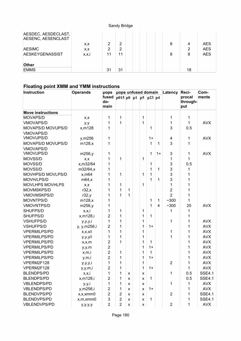
Sandy Bridge
Page 180
x,x 2 2 8 4 AESAESIMC x,x 2 2 2 AESAESKEYGENASSIST x,x,i 11 11 8 8 AES
OtherEMMS 31 31 18
Floating point XMM and YMM instructionsInstruction Operands μops unfused domain Latency
p015 p0 p1 p5 p23 p4
Move instructionsMOVAPS/D x,x 1 1 1 1 1VMOVAPS/D y,y 1 1 1 1 1 AVXMOVAPS/D MOVUPS/D x,m128 1 1 3 0.5
y,m256 1 1+ 4 1 AVXMOVAPS/D MOVUPS/D m128,x 1 1 1 3 1
m256,y 1 1 1+ 3 1 AVXMOVSS/D x,x 1 1 1 1 1MOVSS/D x,m32/64 1 1 3 0.5MOVSS/D m32/64,x 1 1 1 3 1MOVHPS/D MOVLPS/D x,m64 1 1 1 1 3 1MOVH/LPS/D m64,x 1 1 1 3 1MOVLHPS MOVHLPS x,x 1 1 1 1 1MOVMSKPS/D r32,x 1 1 1 2 1VMOVMSKPS/D r32,y 1 1 1 2 1MOVNTPS/D m128,x 1 1 1 ~300 1VMOVNTPS/D m256,y 1 1 4 ~300 25 AVXSHUFPS/D x,x,i 1 1 1 1 1SHUFPS/D x,m128,i 2 1 1 1 1VSHUFPS/D y,y,y,i 1 1 1 1 1 AVXVSHUFPS/D y, y,m256,i 2 1 1 1+ 1 AVXVPERMILPS/PD x,x,x/i 1 1 1 1 1 AVXVPERMILPS/PD y,y,y/i 1 1 1 1 1 AVXVPERMILPS/PD x,x,m 2 1 1 1 1 AVXVPERMILPS/PD y,y,m 2 1 1+ 1 AVXVPERMILPS/PD x,m,i 2 1 1 1 1 AVXVPERMILPS/PD y,m,i 2 1 1 1+ 1 AVXVPERM2F128 y,y,y,i 1 1 1 2 1 AVXVPERM2F128 y,y,m,i 2 1 1 1+ 1 AVXBLENDPS/PD x,x,i 1 1 x x 1 0.5 SSE4.1BLENDPS/PD x,m128,i 2 1 x x 1 0.5 SSE4.1VBLENDPS/PD y,y,i 1 1 x x 1 1 AVXVBLENDPS/PD y,m256,i 2 1 x x 1+ 1 AVXBLENDVPS/PD x,x,xmm0 2 2 x x 2 1 SSE4.1BLENDVPS/PD x,m,xmm0 3 2 x x 1 1 SSE4.1VBLENDVPS/PD y,y,y,y 2 2 x x 2 1 AVX
AESDEC, AESDECLAST, AESENC, AESENCLAST
μops fused do-main
Reci-procal through-put
Com-ments
VMOVAPS/D VMOVUPS/D
VMOVAPS/D VMOVUPS/D

Sandy Bridge
Page 181
VBLENDVPS/PD y,y,m,y 3 2 x x 1+ 1 AVXMOVDDUP x,x 1 1 1 1 1 SSE3MOVDDUP x,m64 1 1 3 0.5 SSE3VMOVDDUP y,y 1 1 1 1 1 AVXVMOVDDUP y,m256 1 1+ 3 1 AVXVBROADCASTSS x,m32 1 1 1 AVXVBROADCASTSS y,m32 2 1 1 1 1 AVXVBROADCASTSD y,m64 2 1 1 1 1 AVXVBROADCASTF128 y,m128 2 1 1 1 1 AVXMOVSH/LDUP x,x 1 1 1 1 1 SSE3MOVSH/LDUP x,m128 1 1 3 0.5 SSE3VMOVSH/LDUP y,y 1 1 1 1 1 AVXVMOVSH/LDUP y,m256 1 1+ 4 1 AVXUNPCKH/LPS/D x,x 1 1 1 1 1 SSE3UNPCKH/LPS/D x,m128 1 1 1 1 1 SSE3VUNPCKH/LPS/D y,y,y 1 1 1 1 1 AVXVUNPCKH/LPS/D y,y,m256 1 1 1 1+ 1 AVXEXTRACTPS r32,x,i 2 2 1 1 2 1 SSE4.1EXTRACTPS m32,x,i 3 2 1 1 1 1 SSE4.1VEXTRACTF128 x,y,i 1 1 1 2 1 AVXVEXTRACTF128 m128,y,i 2 1 1 1 1 AVXINSERTPS x,x,i 1 1 1 1 1 SSE4.1INSERTPS x,m32,i 2 1 1 1 1 SSE4.1VINSERTF128 y,y,x,i 1 1 1 2 1 AVXVINSERTF128 y,y,m128,i 2 1 1 1 1 AVXVMASKMOVPS/D x,x,m128 3 2 1 1 AVXVMASKMOVPS/D y,y,m256 3 2 1+ 1 AVXVMASKMOVPS/D m128,x,x 4 2 1 1 1 AVXVMASKMOVPS/D m256,y,y 4 2 1 1+ 2 AVX
ConversionCVTPD2PS x,x 2 2 1 1 4 1CVTPD2PS x,m128 2 2 1 1 1 1VCVTPD2PS x,y 2 2 1 1 4 1 AVXVCVTPD2PS x,m256 2 2 1 1 1+ 1 AVXCVTSD2SS x,x 2 2 1 1 3 1CVTSD2SS x,m64 2 2 1 1 1 1CVTPS2PD x,x 2 2 1 1 3 1CVTPS2PD x,m64 2 1 1 1 1VCVTPS2PD y,x 2 2 1 1 4 1 AVXVCVTPS2PD y,m128 3 2 1 1 1 1 AVXCVTSS2SD x,x 2 2 1 1 3 1CVTSS2SD x,m32 2 1 1 1 1CVTDQ2PS x,x 1 1 1 3 1CVTDQ2PS x,m128 1 1 1 1 1VCVTDQ2PS y,y 1 1 1 3 1 AVXVCVTDQ2PS y,m256 1 1 1 1+ 1 AVXCVT(T) PS2DQ x,x 1 1 1 3 1CVT(T) PS2DQ x,m128 1 1 1 1 1VCVT(T) PS2DQ y,y 1 1 1 3 1 AVXVCVT(T) PS2DQ y,m256 1 1 1 1+ 1 AVXCVTDQ2PD x,x 2 2 1 1 4 1CVTDQ2PD x,m64 2 2 1 1 1 1

Sandy Bridge
Page 182
VCVTDQ2PD y,x 2 2 1 1 5 1 AVXVCVTDQ2PD y,m128 3 2 1 1 1 1 AVXCVT(T)PD2DQ x,x 2 2 1 1 4 1CVT(T)PD2DQ x,m128 2 2 1 1 1 1VCVT(T)PD2DQ x,y 2 2 1 1 5 1 AVXVCVT(T)PD2DQ x,m256 2 2 1 1 1+ 1 AVXCVTPI2PS x,mm 1 1 1 4 2CVTPI2PS x,m64 1 1 1 1 2CVT(T)PS2PI mm,x 2 2 1 1 4 1CVT(T)PS2PI mm,m128 2 1 1 1 1CVTPI2PD x,mm 2 2 1 1 4 1CVTPI2PD x,m64 2 2 1 1 1 1CVT(T) PD2PI mm,x 2 2 4 1CVT(T) PD2PI mm,m128 2 2 1 1CVTSI2SS x,r32 2 2 1 1 4 1,5CVTSI2SS x,m32 1 1 1 1 1,5CVT(T)SS2SI r32,x 2 2 1 1 4 1CVT(T)SS2SI r32,m32 2 2 1 1 1CVTSI2SD x,r32 2 2 1 1 4 1,5CVTSI2SD x,m32 1 1 1 1 1,5CVT(T)SD2SI r32,x 2 2 1 1 4 1CVT(T)SD2SI r32,m64 2 2 1 1 1 1
ArithmeticADDSS/D SUBSS/D x,x 1 1 1 3 1ADDSS/D SUBSS/D x,m32/64 1 1 1 1 1ADDPS/D SUBPS/D x,x 1 1 1 3 1ADDPS/D SUBPS/D x,m128 1 1 1 1 1VADDPS/D VSUBPS/D y,y,y 1 1 1 3 1 AVXVADDPS/D VSUBPS/D y,y,m256 1 1 1 1+ 1 AVXADDSUBPS/D x,x 1 1 1 3 1 SSE3ADDSUBPS/D x,m128 1 1 1 1 1 SSE3VADDSUBPS/D y,y,y 1 1 1 3 1 AVXVADDSUBPS/D y,y,m256 1 1 1 1+ 1 AVXHADDPS/D HSUBPS/D x,x 3 3 1 2 5 2 SSE3HADDPS/D HSUBPS/D x,m128 4 3 1 2 1 2 SSE3
y,y,y 3 3 1 2 5 2 AVX
y,y,m256 4 3 1 2 1+ 2 AVXMULSS MULPS x,x 1 1 1 5 1MULSS MULPS x,m 1 1 1 1 1VMULPS y,y,y 1 1 1 5 1 AVXVMULPS y,y,m256 1 1 1 1+ 1 AVXMULSD MULPD x,x 1 1 1 5 1MULSD MULPD x,m 1 1 1 1 1VMULPD y,y,y 1 1 1 5 1 AVXVMULPD y,y,m256 1 1 1 1+ 1 AVXDIVSS DIVPS x,x 1 1 1 10-14 10-14DIVSS DIVPS x,m 1 1 1 1 10-14VDIVPS y,y,y 3 3 2 1 21-29 20-28 AVXVDIVPS y,y,m256 4 3 2 1 1+ 20-28 AVXDIVSD DIVPD x,x 1 1 1 10-22 10-22
VHADDPS/D VHSUBPS/DVHADDPS/D VHSUBPS/D

Sandy Bridge
Page 183
DIVSD DIVPD x,m 1 1 1 1 10-22VDIVPD y,y,y 3 3 2 1 21-45 20-44 AVXVDIVPD y,y,m256 4 3 2 1 1+ 20-44 AVXRCPSS/PS x,x 1 1 1 5 1RCPSS/PS x,m128 1 1 1 1 1VRCPPS y,y 3 3 2 1 7 2 AVXVRCPPS y,m256 4 3 1+ 2 AVXCMPccSS/D CMPccPS/D
x,x 1 1 1 3 1CMPccSS/D CMPccPS/D
x,m128 2 1 1 1 1VCMPccPS/D y,y,y 1 1 1 3 1 AVXVCMPccPS/D y,y,m256 2 1 1 1+ 1 AVXCOMISS/D UCOMISS/D x,x 2 2 1 1 2 1COMISS/D UCOMISS/D x,m32/64 2 2 1 1 1 1MAXSS/D MINSS/D x,x 1 1 1 3 1MAXSS/D MINSS/D x,m32/64 1 1 1 1 1MAXPS/D MINPS/D x,x 1 1 1 3 1MAXPS/D MINPS/D x,m128 1 1 1 1 1VMAXPS/D VMINPS/D y,y,y 1 1 1 3 1 AVXVMAXPS/D VMINPS/D y,y,m256 1 1 1 1+ 1 AVXROUNDSS/SD/PS/PD x,x,i 1 1 1 3 1 SSE4.1ROUNDSS/SD/PS/PD x,m128,i 2 1 1 1 1 SSE4.1VROUNDSS/SD/PS/PD y,y,i 1 1 1 3 1 AVXVROUNDSS/SD/PS/PD y,m256,i 2 1 1 1+ 1 AVXDPPS x,x,i 4 4 1 2 1 12 2 SSE4.1DPPS x,m128,i 6 5 1 4 SSE4.1VDPPS y,y,y,i 4 4 1 2 1 12 2 AVXVDPPS y,m256,i 6 5 1+ 4 AVXDPPD x,x,i 3 3 1 1 1 9 2 SSE4.1DPPD x,m128,i 4 3 1 2 SSE4.1
MathSQRTSS/PS x,x 1 1 1 10-14 10-14SQRTSS/PS x,m128 1 1 1 1 10-14VSQRTPS y,y 3 3 21-28 AVXVSQRTPS y,m256 4 3 1+ 21-28 AVXSQRTSD/PD x,x 1 1 1 10-21 10-21SQRTSD/PD x,m128 2 1 1 1 10-21VSQRTPD y,y 3 3 21-43 21-43 AVXVSQRTPD y,m256 4 3 1+ 21-43 AVXRSQRTSS/PS x,x 1 1 1 5 1RSQRTSS/PS x,m128 1 1 1 1 1VRSQRTPS y,y 3 3 7 2 AVXVRSQRTPS y,m256 4 3 1+ 2 AVX
LogicAND/ANDN/OR/XORPS/PD x,x 1 1 1 1 1AND/ANDN/OR/XORPS/PD x,m128 1 1 1 1 1
y,y,y 1 1 1 1 1 AVX
y,y,m256 1 1 1 1+ 1 AVX
VAND/ANDN/OR/XORPS/PD
VAND/ANDN/OR/XORPS/PD

Sandy Bridge
Page 184
(V)XORPS/PD x/y,x/y,same 1 0 0 0.25
OtherVZEROUPPER 4 2 1 AVX
VZEROALL 12 11
VZEROALL 20 9LDMXCSR m32 3 3 1 3STMXCSR m32 3 3 1 1 1 1 1VSTMXCSR m32 3 3 1 1 1 1 1 AVXFXSAVE m4096 130 68FXRSTOR m4096 116 72XSAVEOPT m 100-161 60-500
AVX,32 bit
AVX,64 bit

Ivy Bridge
Page 185
Intel Ivy BridgeList of instruction timings and μop breakdown
Explanation of column headings:Operands:
μops fused domain:
μops unfused domain:
p015: The total number of μops going to port 0, 1 and 5.p0: The number of μops going to port 0 (execution units).p1: The number of μops going to port 1 (execution units). p5: The number of μops going to port 5 (execution units). p23: The number of μops going to port 2 or 3 (memory read or address calculation).
p4: The number of μops going to port 4 (memory write data).Latency:
Reciprocal throughput:
Integer instructionsInstruction Operands μops unfused domain Latency
p015 p0 p1 p5 p23 p4
i = immediate data, r = register, mm = 64 bit mmx register, x = 128 bit xmm register, (x)mm = mmx or xmm register, y = 256 bit ymm register, same = same register for both operands. m = memory operand, m32 = 32-bit memory operand, etc.
The number of μops at the decode, rename, allocate and retirement stages in the pipeline. Fused μops count as one.
The number of μops for each execution port. Fused μops count as two. Fused macro-ops count as one. The instruction has μop fusion if the sum of the numbers listed under p015 + p23 + p4 exceeds the number listed under μops fused domain. A number indicated as 1+ under a read or write port means a 256-bit read or write operation using two clock cycles for handling 128 bits each cycle. The port cannot receive another read or write µop in the second clock cycle, but a read port can receive an address-calculation µop in the sec-ond clock cycle. An x under p0, p1 or p5 means that at least one of the μops listed under p015 can optionally go to this port. For example, a 1 under p015 and an x under p0 and p5 means one μop which can go to either port 0 or port 5, whichever is vacant first. A value listed under p015 but nothing under p0, p1 and p5 means that it is not known which of the three ports these μops go to.
This is the delay that the instruction generates in a dependency chain. The numbers are minimum values. Cache misses, misalignment, and exceptions may increase the clock counts considerably. Where hyperthreading is enabled, the use of the same execution units in the other thread leads to inferior per-formance. Denormal numbers, NAN's and infinity do not increase the latency. The time unit used is core clock cycles, not the reference clock cycles given by the time stamp counter.
The average number of core clock cycles per instruction for a series of inde-pendent instructions of the same kind in the same thread.
The latencies and throughputs listed below for addition and multiplication using full size YMM registers are obtained only after a warm-up period of a thousand instructions or more. The latencies may be one or two clock cycles longer and the reciprocal throughputs double the values for shorter sequences of code. There is no warm-up effect when vectors are 128 bits wide or less.
μops fused do-main
Reci-procal through-put
Com-ments

Ivy Bridge
Page 186
Move instructionsMOV r,i 1 1 x x x 1 0.33MOV r8/16,r8/16 1 1 x x x 1 0.33MOV r32/64,r32/64 1 1 x x x 0-1 0.25
MOV r8/16,m8/16 1 1 x x x 1 2 0.5MOV r32/64,m32/64 1 1 2 0.5MOV r,m 1 1 2 1
MOV m,r 1 1 1 3 1MOV m,i 1 1 1 1MOVNTI m,r 2 1 1 ~340 1MOVSX MOVSXD r,r 1 1 x x x 1 0.33MOVZX r16,r8 1 1 x x x 1 0.33MOVZX r32/64,r8 1 1 x x x 0-1 0.25
MOVZX r32/64,r16 1 1 x x x 1 0.33MOVSX MOVZX r16,m8 2 1 x x x 1 3 0.5
r32/64,m 1 1 2 0.5
CMOVcc r,r 2 2 x x x 2 0.67CMOVcc r,m 2 2 x x x 1 ~0.8XCHG r,r 3 3 x x x 2 1XCHG r,m 7 x 2 3 25
XLAT 3 2 1 7 1PUSH r 1 1 1 3 1PUSH i 1 1 1 1PUSH m 2 2 1 1PUSH (E/R)SP 2 1 x x x 1 1 3 1PUSHF(D/Q) 3 2 x x x 1 1 1PUSHA(D) 19 3 x x x 8 8 8 not 64 bit
POP r 1 1 2 0.5POP (E/R)SP 3 2 x x x 1 0.5POP m 2 2 1 1POPF(D/Q) 9 8 x x x 1 18POPA(D) 18 10 x x x 8 9 not 64 bit
LAHF SAHF 1 1 x x 1 1SALC 3 3 x x x 1 1 not 64 bit
LEA r16,m 2 2 x 1 x 2-4 1LEA r32/64,m 1 1 x x 1 0.5
LEA r32/64,m 1 1 1 3 1
BSWAP r32 1 1 1 1 1BSWAP r64 2 2 x 1 x 2 1PREFETCHNTA m 1 1 43PREFETCHT0/1/2 m 1 1 43LFENCE 2 4MFENCE 3 1 1 36SFENCE 2 1 1 6
may be elimin.
64 b absaddress
may be elimin.
MOVSX MOVZX MOVSXD
implicit lock
1-2 com-ponents
3 com-ponents or RIP

Ivy Bridge
Page 187
Arithmetic instructionsADD SUB r,r/i 1 1 x x x 1 0.33ADD SUB r,m 1 1 x x x 1 0.5ADD SUB m,r/i 2 1 x x x 2 1 6 1ADC SBB r,r/i 2 2 x x x 2 1ADC SBB r,m 2 2 x x x 1 2 1ADC SBB m,r/i 4 3 x x x 2 1 7-8 2CMP r,r/i 1 1 x x x 1 0.33CMP m,r/i 1 1 x x x 1 1 0.5INC DEC NEG NOT r 1 1 x x x 1 0.33INC DEC NEG NOT m 3 1 x x x 2 1 6 1AAA AAS 2 2 x 1 x 4 not 64 bit
DAA DAS 3 3 4 not 64 bit
AAD 3 3 2 not 64 bit
AAM 8 8 20 8 not 64 bit
MUL IMUL r8 1 1 1 3 1MUL IMUL r16 4 4 4 2MUL IMUL r32 3 3 4 2MUL IMUL r64 2 2 3 1IMUL r,r 1 1 1 3 1IMUL r16,r16,i 2 2 4 1IMUL r32,r32,i 1 1 1 3 1IMUL r64,r64,i 1 1 1 3 1MUL IMUL m8 1 1 1 1 3 1MUL IMUL m16 4 3 1 2MUL IMUL m32 3 2 1 2MUL IMUL m64 2 1 1 2IMUL r,m 1 1 1 1 1IMUL r16,m16,i 2 2 1 1IMUL r32,m32,i 1 1 1 1 1IMUL r64,m64,i 1 1 1 1 1DIV r8 11 11 19-22 9DIV r16 11 11 20-24 10DIV r32 10 10 19-27 11DIV r64 35-57 x 29-94 22-76IDIV r8 11 11 20-23 8IDIV r16 11 11 20-24 8IDIV r32 9 9 19-26 8-11IDIV r64 x 28-103 26-88
CBW 1 1 x x x 1 0.33CWDE 1 1 x x x 1CDQE 1 1 x x x 1CWD 2 2 x x x 1CDQ 1 1 x x 1CQO 1 1 x x 1 0.5POPCNT r,r 1 1 1 3 1 SSE4.2POPCNT r,m 1 1 1 1 1 SSE4.2CRC32 r,r 1 1 1 3 1 SSE4.2CRC32 r,m 1 1 1 1 SSE4.2
Logic instructions
59-134

Ivy Bridge
Page 188
AND OR XOR r,r/i 1 1 x x x 1 0.33AND OR XOR r,m 1 1 x x x 1 0.5AND OR XOR m,r/i 2 1 x x x 2 1 6 1TEST r,r/i 1 1 x x x 1 0.33TEST m,r/i 1 1 x x x 1 0.5SHR SHL SAR r,i 1 1 x x 1 0.5SHR SHL SAR m,i 3 1 2 1 2SHR SHL SAR r,cl 2 2 1 1 1 1SHR SHL SAR m,cl 5 3 2 1 4ROR ROL r,1 2 2 x x 1 1 short form
ROR ROL r,i 1 1 x x 1 0.5ROR ROL m,i 4 3 2 1 2ROR ROL r,cl 2 2 x x 1 1ROR ROL m,cl 5 3 2 1 4RCL RCR r,1 3 3 x x x 2 2RCL RCR r,i 8 8 x x x 5 5RCL RCR m,i 11 8 x x x 2 1 6RCL RCR r,cl 8 8 x x x 5 5RCL RCR m,cl 11 8 x x x 2 1 6SHRD SHLD r,r,i 1 1 x x 1 0.5SHRD SHLD m,r,i 3 3 x x x 2 1 2SHRD SHLD r,r,cl 4 4 x 1 x 2 2SHRD SHLD m,r,cl 5 4 x 1 x 2 1 4BT r,r/i 1 1 x x 1 0.5BT m,r 10 9 x x x 1 5BT m,i 2 1 x x 1 0.5BTR BTS BTC r,r/i 1 1 x x 1 0.5BTR BTS BTC m,r 11 8 x x x 2 1 5BTR BTS BTC m,i 3 2 x x 1 1 2BSF BSR r,r 1 1 1 3 1BSF BSR r,m 1 1 1 1 1SETcc r 1 1 x x 1 0.5SETcc m 2 1 x x 1 1 1CLC 1 0 0.25STC CMC 1 1 x x x 1 0.33CLD STD 3 3 x x x 4
Control transfer instructionsJMP short/near 1 1 1 0 2JMP r 1 1 1 0 2JMP m 1 1 1 1 0 2Conditional jump short/near 1 1 1 0 1-2
1 1 1 0 1-2
J(E/R)CXZ short 2 2 x x 1 1-2LOOP short 7 7 4-5LOOP(N)E short 11 11 6CALL near 2 1 1 1 1 2CALL r 2 1 1 1 1 2CALL m 3 1 1 2 1 2RET 2 1 1 1 2RET i 3 2 x x 1 1 2
fast if no jump
Fused arithmetic and branch
fast if no jump

Ivy Bridge
Page 189
BOUND r,m 15 13 2 7 not 64 bit
INTO 4 4 x x x 6 not 64 bit
String instructionsLODS 3 2 x x x 1 1REP LODS ~5n ~2nSTOS 3 1 x x x 1 1 1REP STOS many n
REP STOS many 1/16B
MOVS 5 2 x x x 2 1 4REP MOVS 2n n
REP MOVS 4/16B 1/16B
SCAS 3 2 x x x 1 1REP SCAS ~6n ~2nCMPS 5 3 x x x 2 4REP CMPS ~8n ~2n
Synchronization instructionsXADD m,r 4 3 x x x 1 1 7LOCK XADD m,r 8 5 x x x 2 1 22LOCK ADD m,r 7 5 x x x 1 1 22CMPXCHG m,r 5 3 x x x 2 1 7LOCK CMPXCHG m,r 9 6 x x x 2 1 22CMPXCHG8B m,r 14 11 x x x 2 1 7LOCK CMPXCHG8B m,r 18 15 x x x 2 1 22CMPXCHG16B m,r 22 19 x x x 2 1 16LOCK CMPXCHG16B m,r 24 21 x x x 2 1 27
OtherNOP / Long NOP 1 0 0.25PAUSE 7 7 10ENTER a,0 12 9 x x x 2 1 8ENTER a,b 45+7b 84+3bLEAVE 3 2 x x x 1 6XGETBV 8 9 XGETBV
CPUID 37-82 100-340RDTSC 21 27RDPMC 35 39RDRAND r 13 12 x x x 1 104-117 RDRAND
Floating point x87 instructionsInstruction Operands μops unfused domain Latency
p015 p0 p1 p5 p23 p4
Move instructions
worst case
best case
worst case
best case
μops fused do-main
Reci-procal through-put
Com-ments

Ivy Bridge
Page 190
FLD r 1 1 1 1 1FLD m32/64 1 1 3 1FLD m80 4 2 1 1 2 5 2FBLD m80 43 40 3 45 21FST(P) r 1 1 1 1 1FST(P) m32/m64 1 1 1 4 1FSTP m80 7 3 2 2 5 5FBSTP m80 243 252FXCH r 1 0 0 0.5FILD m 1 1 1 1 6 1FIST(P) m 3 1 1 1 1 7 1FISTTP m 3 1 1 1 1 7 2 SSE3FLDZ 1 1 1FLD1 2 2 1 1FLDPI FLDL2E etc. 2 2 1 1 2FCMOVcc r 3 3 1 2 2 2FNSTSW AX 2 2 1 x x 4 1FNSTSW m16 2 1 1 1 1FLDCW m16 3 2 2 1 3FNSTCW m16 2 1 1 1 1 1FINCSTP FDECSTP 1 1 1 1 1FFREE(P) r 1 1 1 1FNSAVE m 143 167FRSTOR m 90 162
Arithmetic instructionsFADD(P) FSUB(R)(P) r 1 1 1 3 1FADD(P) FSUB(R)(P) m 2 1 1 1 1FMUL(P) r 1 1 1 5 1FMUL(P) m 2 1 1 1 1FDIV(R)(P) r 1 1 1 10-24 8-18FDIV(R)(P) m 2 1 1 1 8-18FABS 1 1 1 1 1FCHS 1 1 1 1 1FCOM(P) FUCOM r 1 1 1 3 1FCOM(P) FUCOM m 1 1 1 1 1FCOMPP FUCOMPP 2 2 1 1 4 1FCOMI(P) FUCOMI(P) r 3 3 1 1 1 5 1FIADD FISUB(R) m 2 2 2 1 2FIMUL m 2 2 1 1 1 2FIDIV(R) m 2 2 1 1 1FICOM(P) m 2 2 2 1 2FTST 1 1 1 1FXAM 2 2 2 2FPREM 28 28 21-26 12FPREM1 41 27-50 19FRNDINT 17 17 22 11
MathFSCALE 25 25 x x x 49 49FXTRACT 17 17 x x x 10 10FSQRT 1 1 1 10-23 8-17FSIN 21-78 x x x 47-106 47-106

Ivy Bridge
Page 191
FCOS 23-100 x x x 48-115 48-115FSINCOS 20-110 x x x 50-123 50-123F2XM1 16-23 x x x ~68 ~68FYL2X 42 42 x x x 90-106FYL2XP1 56 56 x x x 82FPTAN 102 102 x x x 130FPATAN 28-72 x x x 94-150
OtherFNOP 1 1 1 1WAIT 2 2 x x 1 1FNCLEX 5 5 x x x 22FNINIT 26 26 x x x 80
Integer MMX and XMM instructionsInstruction Operands μops unfused domain Latency
p015 p0 p1 p5 p23 p4
Move instructionsMOVD r32/64,(x)mm 1 1 1 1 1MOVD m32/64,(x)mm 1 1 1 3 1MOVD (x)mm,r32/64 1 1 1 1 1MOVD (x)mm,m32/64 1 1 3 0.5MOVQ (x)mm,(x)mm 1 1 x x x 1 0.33MOVQ (x)mm,m64 1 1 3 0.5MOVQ m64, (x)mm 1 1 1 3 1MOVDQA MOVDQU x,x 1 1 x x x 0-1 0.25 eliminat.MOVDQA MOVDQU x, m128 1 1 3 0.5MOVDQA MOVDQU m128, x 1 1 1 3 1LDDQU x, m128 1 1 1 3 0.5 SSE3MOVDQ2Q mm, x 2 2 x x 1 1 1MOVQ2DQ x,mm 1 1 1 0.33MOVNTQ m64,mm 1 1 1 ~360 1MOVNTDQ m128,x 1 1 1 ~360 1MOVNTDQA x, m128 1 1 3 0.5 SSE4.1
mm,mm 1 1 1 1 1
mm,m64 1 1 1 1 1
x,x 1 1 x x 1 0.5
x,m128 1 1 x x 1 1 0.5PACKUSDW x,x 1 1 x x 1 0.5 SSE4.1PACKUSDW x,m 1 1 x x 1 0.5 SSE4.1PUNPCKH/LBW/WD/DQ (x)mm,(x)mm 1 1 x x 1 0.5PUNPCKH/LBW/WD/DQ (x)mm,m 1 1 x x 1 0.5PUNPCKH/LQDQ x,x 1 1 x x 1 0.5PUNPCKH/LQDQ x, m128 2 1 x x 1 0.5PMOVSX/ZXBW x,x 1 1 x x 1 0.5 SSE4.1
μops fused do-main
Reci-procal through-put
Com-ments
PACKSSWB/DW PACKUSWB
PACKSSWB/DW PACKUSWB
PACKSSWB/DW PACKUSWB
PACKSSWB/DW PACKUSWB

Ivy Bridge
Page 192
PMOVSX/ZXBW x,m64 1 1 x x 1 0.5 SSE4.1PMOVSX/ZXBD x,x 1 1 x x 1 0.5 SSE4.1PMOVSX/ZXBD x,m32 1 1 x x 1 0.5 SSE4.1PMOVSX/ZXBQ x,x 1 1 x x 1 0.5 SSE4.1PMOVSX/ZXBQ x,m16 1 1 x x 1 0.5 SSE4.1PMOVSX/ZXWD x,x 1 1 x x 1 0.5 SSE4.1PMOVSX/ZXWD x,m64 1 1 x x 1 0.5 SSE4.1PMOVSX/ZXWQ x,x 1 1 x x 1 0.5 SSE4.1PMOVSX/ZXWQ x,m32 1 1 x x 1 0.5 SSE4.1PMOVSX/ZXDQ x,x 1 1 x x 1 0.5 SSE4.1PMOVSX/ZXDQ x,m64 1 1 x x 1 0.5 SSE4.1PSHUFB (x)mm,(x)mm 1 1 x x 1 0.5 SSSE3PSHUFB (x)mm,m 2 1 x x 1 0.5 SSSE3PSHUFW mm,mm,i 1 1 x x 1 0.5PSHUFW mm,m64,i 2 1 x x 1 0.5PSHUFD xmm,x,i 1 1 x x 1 0.5PSHUFD x,m128,i 2 1 x x 1 0.5PSHUFL/HW x,x,i 1 1 x x 1 0.5PSHUFL/HW x, m128,i 2 1 x x 1 0.5PALIGNR (x)mm,(x)mm,i 1 1 x x 1 0.5 SSSE3PALIGNR (x)mm,m,i 2 1 x x 1 0.5 SSSE3PBLENDVB x,x,xmm0 2 2 1 1 2 1 SSE4.1PBLENDVB x,m,xmm0 3 2 1 1 1 1 SSE4.1PBLENDW x,x,i 1 1 x x 1 0.5 SSE4.1PBLENDW x,m,i 2 1 x x 1 0.5 SSE4.1MASKMOVQ mm,mm 4 1 1 2 1 1MASKMOVDQU x,x 10 4 x 1 x 4 2 6PMOVMSKB r32,(x)mm 1 1 1 2 1PEXTRB r32,x,i 2 2 1 x x 2 1 SSE4.1PEXTRB m8,x,i 2 1 x x 1 1 1 SSE4.1PEXTRW r32,(x)mm,i 2 1 1 x x 2 1PEXTRW m16,(x)mm,i 2 1 x x 1 1 1 SSE4.1PEXTRD r32,x,i 2 2 1 x x 2 1 SSE4.1PEXTRD m32,x,i 2 1 x x 1 1 1 SSE4.1PEXTRQ r64,x,i 2 2 1 x x 2 1 SSE4.1PEXTRQ m64,x,i 2 1 x x 1 1 1PINSRB x,r32,i 2 2 x x 2 1 SSE4.1PINSRB x,m8,i 2 1 x x 1 0.5 SSE4.1PINSRW (x)mm,r32,i 2 2 x x 2 1PINSRW (x)mm,m16,i 2 1 x x 1 0.5PINSRD x,r32,i 2 1 x x 2 1 SSE4.1PINSRD x,m32,i 2 1 x x 1 0.5 SSE4.1PINSRQ x,r64,i 2 1 x x 2 1 SSE4.1PINSRQ x,m64,i 2 1 x x 1 0.5 SSE4.1
Arithmetic instructionsPADD/SUB(U,S)B/W/D/Q (x)mm, (x)mm 1 1 x x 1 0.5PADD/SUB(U,S)B/W/D/Q (x)mm,m 1 1 x x 1 0.5PHADD/SUB(S)W/D (x)mm, (x)mm 3 3 x x 3 1,5 SSSE3PHADD/SUB(S)W/D (x)mm,m64 4 3 x x 1 1,5 SSSE3PCMPEQ/GTB/W/D (x)mm,(x)mm 1 1 x x 1 0.5PCMPEQ/GTB/W/D (x)mm,m 1 1 x x 1 0.5PCMPEQQ x,x 1 1 x x 1 0.5 SSE4.1

Ivy Bridge
Page 193
PCMPEQQ x,m128 1 1 x x 1 0.5 SSE4.1PCMPGTQ x,x 1 1 1 5 1 SSE4.2PCMPGTQ x,m128 1 1 1 1 1 SSE4.2PMULL/HW PMULHUW (x)mm,(x)mm 1 1 1 5 1PMULL/HW PMULHUW (x)mm,m 1 1 1 1 1PMULHRSW (x)mm,(x)mm 1 1 1 5 1 SSSE3PMULHRSW (x)mm,m 1 1 1 1 1 SSSE3PMULLD x,x 1 1 1 5 1 SSE4.1PMULLD x,m128 2 1 1 1 1 SSE4.1PMULDQ x,x 1 1 1 5 1 SSE4.1PMULDQ x,m128 1 1 1 1 1 SSE4.1PMULUDQ (x)mm,(x)mm 1 1 1 5 1PMULUDQ (x)mm,m 1 1 1 1 1PMADDWD (x)mm,(x)mm 1 1 1 5 1PMADDWD (x)mm,m 1 1 1 1 1PMADDUBSW (x)mm,(x)mm 1 1 1 5 1 SSSE3PMADDUBSW (x)mm,m 1 1 1 1 1 SSSE3PAVGB/W (x)mm,(x)mm 1 1 x x 1 0.5PAVGB/W (x)mm,m 1 1 x x 1 0.5PMIN/MAXSB x,x 1 1 x x 1 0.5 SSE4.1PMIN/MAXSB x,m128 1 1 x x 1 0.5 SSE4.1PMIN/MAXUB (x)mm,(x)mm 1 1 x x 1 0.5PMIN/MAXUB (x)mm,m 1 1 x x 1 0.5PMIN/MAXSW (x)mm,(x)mm 1 1 x x 1 0.5PMIN/MAXSW (x)mm,m 1 1 x x 1 0.5PMIN/MAXUW x,x 1 1 x x 1 0.5 SSE4.1PMIN/MAXUW x,m 1 1 x x 1 0.5 SSE4.1PMIN/MAXU/SD x,x 1 1 x x 1 0.5 SSE4.1PMIN/MAXU/SD x,m128 1 1 x x 1 0.5 SSE4.1PHMINPOSUW x,x 1 1 1 5 1 SSE4.1PHMINPOSUW x,m128 1 1 1 1 1 SSE4.1PABSB/W/D (x)mm,(x)mm 1 1 x x 1 0.5 SSSE3PABSB/W/D (x)mm,m 1 1 x x 1 0.5 SSSE3PSIGNB/W/D (x)mm,(x)mm 1 1 x x 1 0.5 SSSE3PSIGNB/W/D (x)mm,m 1 1 x x 1 0.5 SSSE3PSADBW (x)mm,(x)mm 1 1 1 5 1PSADBW (x)mm,m 1 1 1 1 1MPSADBW x,x,i 3 3 1 1 1 6 1 SSE4.1MPSADBW x,m,i 4 3 1 1 1 1 1 SSE4.1
Logic instructionsPAND(N) POR PXOR (x)mm,(x)mm 1 1 x x x 1 0.33PAND(N) POR PXOR (x)mm,m 1 1 x x x 1 0.5PTEST x,x 2 2 1 x x 1 1 SSE4.1PTEST x,m128 3 2 1 x x 1 1 SSE4.1PSLL/RL/RAW/D/Q mm,mm/i 1 1 1 1 1PSLL/RL/RAW/D/Q mm,m64 1 1 1 1 1PSLL/RL/RAW/D/Q xmm,i 1 1 1 1 1PSLL/RL/RAW/D/Q x,x 2 2 1 x x 2 1PSLL/RL/RAW/D/Q x,m128 3 2 1 x x 1 1PSLL/RLDQ x,i 1 1 x x 1 0.5
String instructions

Ivy Bridge
Page 194
PCMPESTRI x,x,i 8 8 3 1 4 4 4 SSE4.2PCMPESTRI x,m128,i 8 7 3 1 3 1 4 SSE4.2PCMPESTRM x,x,i 8 8 3 1 4 12 4 SSE4.2PCMPESTRM x,m128,i 8 7 3 1 3 1 4 SSE4.2PCMPISTRI x,x,i 3 3 3 3 SSE4.2PCMPISTRI x,m128,i 4 3 3 1 3 SSE4.2PCMPISTRM x,x,i 3 3 3 11 SSE4.2PCMPISTRM x,m128,i 4 3 3 1 3 SSE4.2
Encryption instructionsPCLMULQDQ x,x,i 18 18 x x x 14 8 CLMULPCLMULQDQ x,m,i 18 17 x x x 1 8 CLMUL
x,x 2 2 x x 1 4 1 AES
x,m 3 2 x x 1 1 1 AESAESIMC x,x 2 2 2 14 2 AESAESIMC x,m 3 2 2 1 2 AESAESKEYGENASSIST x,x,i 11 11 x x x 10 8 AESAESKEYGENASSIST x,m,i 11 10 x x x 1 7 AES
OtherEMMS 31 31 18
Floating point XMM and YMM instructionsInstruction Operands μops unfused domain Latency
p015 p0 p1 p5 p23 p4
Move instructionsMOVAPS/D x,x 1 1 1 0-1 ≤1 elimin.VMOVAPS/D y,y 1 1 1 0-1 ≤1 elimin.MOVAPS/D MOVUPS/D x,m128 1 1 3 0.5
y,m256 1 1+ 4 1 AVXMOVAPS/D MOVUPS/D m128,x 1 1 1 3 1
m256,y 1 1 1+ 4 2 AVXMOVSS/D x,x 1 1 1 1 1MOVSS/D x,m32/64 1 1 3 0.5MOVSS/D m32/64,x 1 1 1 3 1MOVHPS/D MOVLPS/D x,m64 2 1 1 1 4 1MOVH/LPS/D m64,x 2 1 1 3 1MOVLHPS MOVHLPS x,x 1 1 1 1 1MOVMSKPS/D r32,x 1 1 1 2 1VMOVMSKPS/D r32,y 1 1 1 2 1MOVNTPS/D m128,x 1 1 1 ~380 1VMOVNTPS/D m256,y 1 1 1+ ~380 2 AVXSHUFPS/D x,x,i 1 1 1 1 1
AESDEC, AESDECLAST, AESENC, AESENCLAST
AESDEC, AESDECLAST, AESENC, AESENCLAST
μops fused do-main
Reci-procal through-put
Com-ments
VMOVAPS/D VMOVUPS/D
VMOVAPS/D VMOVUPS/D

Ivy Bridge
Page 195
SHUFPS/D x,m128,i 2 1 1 1 1VSHUFPS/D y,y,y,i 1 1 1 1 1 AVXVSHUFPS/D y, y,m256,i 2 1 1 1+ 1 AVXVPERMILPS/PD x,x,x/i 1 1 1 1 1 AVXVPERMILPS/PD y,y,y/i 1 1 1 1 1 AVXVPERMILPS/PD x,x,m 2 1 1 1 1 AVXVPERMILPS/PD y,y,m 2 1 1 1+ 1 AVXVPERMILPS/PD x,m,i 2 1 1 1 1 AVXVPERMILPS/PD y,m,i 2 1 1 1+ 1 AVXVPERM2F128 y,y,y,i 1 1 1 2 1 AVXVPERM2F128 y,y,m,i 2 1 1 1+ 1 AVXBLENDPS/PD x,x,i 1 1 x x 1 0.5 SSE4.1BLENDPS/PD x,m128,i 2 1 x x 1 0.5 SSE4.1VBLENDPS/PD y,y,i 1 1 x x 1 0.5 AVXVBLENDPS/PD y,m256,i 2 1 x x 1+ 1 AVXBLENDVPS/PD x,x,xmm0 2 2 x x 2 1 SSE4.1BLENDVPS/PD x,m,xmm0 3 2 x x 1 1 SSE4.1VBLENDVPS/PD y,y,y,y 2 2 x x 2 1 AVXVBLENDVPS/PD y,y,m,y 3 2 x x 1+ 1 AVXMOVDDUP x,x 1 1 1 1 1 SSE3MOVDDUP x,m64 1 1 3 0.5 SSE3VMOVDDUP y,y 1 1 1 1 1 AVXVMOVDDUP y,m256 1 1+ 3 1 AVXVBROADCASTSS x,m32 1 1 4 0.5 AVXVBROADCASTSS y,m32 2 1 1 1 5 1 AVXVBROADCASTSD y,m64 2 1 1 1 5 1 AVXVBROADCASTF128 y,m128 2 1 1 1 5 1 AVXMOVSH/LDUP x,x 1 1 1 1 1 SSE3MOVSH/LDUP x,m128 1 1 3 0.5 SSE3VMOVSH/LDUP y,y 1 1 1 1 1 AVXVMOVSH/LDUP y,m256 1 1+ 1 AVXUNPCKH/LPS/D x,x 1 1 1 1 1 SSE3UNPCKH/LPS/D x,m128 1 1 1 1 1 SSE3VUNPCKH/LPS/D y,y,y 1 1 1 1 1 AVXVUNPCKH/LPS/D y,y,m256 1 1 1 1+ 1 AVXEXTRACTPS r32,x,i 2 2 x x 2 1 SSE4.1EXTRACTPS m32,x,i 3 2 x x 1 1 1 SSE4.1VEXTRACTF128 x,y,i 1 1 1 2 1 AVXVEXTRACTF128 m128,y,i 2 0 1 1 4 1 AVXINSERTPS x,x,i 1 1 1 1 1 SSE4.1INSERTPS x,m32,i 2 1 1 1 1 SSE4.1VINSERTF128 y,y,x,i 1 1 1 2 1 AVXVINSERTF128 y,y,m128,i 2 1 x x 1 4 1 AVXVMASKMOVPS/D x,x,m128 3 2 x x 1 4 1 AVXVMASKMOVPS/D y,y,m256 3 2 1+ 5 1 AVXVMASKMOVPS/D m128,x,x 4 2 x x 1 1 1 AVXVMASKMOVPS/D m256,y,y 4 2 x x 1 1+ 2 AVX
ConversionCVTPD2PS x,x 2 2 1 1 4 1CVTPD2PS x,m128 2 2 1 1 1 1VCVTPD2PS x,y 2 2 1 1 4 1 AVXVCVTPD2PS x,m256 2 2 1 1 1+ 1 AVX

Ivy Bridge
Page 196
CVTSD2SS x,x 2 2 1 1 4 1CVTSD2SS x,m64 2 2 1 1 1 1CVTPS2PD x,x 2 2 1 1 1 1CVTPS2PD x,m64 2 1 1 1 1VCVTPS2PD y,x 2 2 1 1 4 1 AVXVCVTPS2PD y,m128 3 2 1 1 1 1 AVXCVTSS2SD x,x 2 2 1 1 2 1CVTSS2SD x,m32 2 1 1 1 1CVTDQ2PS x,x 1 1 1 3 1CVTDQ2PS x,m128 1 1 1 1 1VCVTDQ2PS y,y 1 1 1 3 1 AVXVCVTDQ2PS y,m256 1 1 1 1+ 1 AVXCVT(T) PS2DQ x,x 1 1 1 3 1CVT(T) PS2DQ x,m128 1 1 1 1 1VCVT(T) PS2DQ y,y 1 1 1 3 1 AVXVCVT(T) PS2DQ y,m256 1 1 1 1+ 1 AVXCVTDQ2PD x,x 2 2 1 1 4 1CVTDQ2PD x,m64 2 2 1 1 1 1VCVTDQ2PD y,x 2 2 1 1 5 1 AVXVCVTDQ2PD y,m128 2 2 1 1 1 1 AVXCVT(T)PD2DQ x,x 2 2 1 1 4 1CVT(T)PD2DQ x,m128 2 2 1 1 1 1VCVT(T)PD2DQ x,y 2 2 1 1 5 1 AVXVCVT(T)PD2DQ x,m256 2 2 1 1 1+ 1 AVXCVTPI2PS x,mm 1 1 1 4CVTPI2PS x,m64 1 1 1 1 3CVT(T)PS2PI mm,x 2 2 1 1 4 1CVT(T)PS2PI mm,m128 2 1 1 1 1CVTPI2PD x,mm 2 2 1 1 4 1CVTPI2PD x,m64 2 2 1 1 1 1CVT(T) PD2PI mm,x 2 2 1 1 4 1CVT(T) PD2PI mm,m128 2 2 1 1 1 1CVTSI2SS x,r32 2 2 1 1 4 3CVTSI2SS x,m32 1 1 1 1 3CVT(T)SS2SI r32,x 2 2 1 1 4 1CVT(T)SS2SI r32,m32 2 2 1 1 1 1CVTSI2SD x,r32 2 2 1 1 4 3CVTSI2SD x,m32 2 1 1 1 3CVT(T)SD2SI r32,x 2 2 1 1 4 1CVT(T)SD2SI r32,m64 2 2 1 1 1 1VCVTPS2PH x,v,i 3 3 1 1 1 10 1 F16CVCVTPS2PH m,v,i 3 2 1 1 1 1 1 F16CVCVTPH2PS v,x 2 2 1 1 6 1 F16CVCVTPH2PS v,m 2 1 1 1 1 F16C
ArithmeticADDSS/D SUBSS/D x,x 1 1 1 3 1ADDSS/D SUBSS/D x,m32/64 1 1 1 1 1ADDPS/D SUBPS/D x,x 1 1 1 3 1ADDPS/D SUBPS/D x,m128 1 1 1 1 1VADDPS/D VSUBPS/D y,y,y 1 1 1 3 1 AVXVADDPS/D VSUBPS/D y,y,m256 1 1 1 1+ 1 AVXADDSUBPS/D x,x 1 1 1 3 1 SSE3

Ivy Bridge
Page 197
ADDSUBPS/D x,m128 1 1 1 1 1 SSE3VADDSUBPS/D y,y,y 1 1 1 3 1 AVXVADDSUBPS/D y,y,m256 1 1 1 1+ 1 AVXHADDPS/D HSUBPS/D x,x 3 3 1 2 5 2 SSE3HADDPS/D HSUBPS/D x,m128 4 3 1 2 1 2 SSE3
y,y,y 3 3 1 2 5 2 AVX
y,y,m256 4 3 1 2 1+ 2 AVXMULSS MULPS x,x 1 1 1 5 1MULSS MULPS x,m 1 1 1 1 1VMULPS y,y,y 1 1 1 5 1 AVXVMULPS y,y,m256 1 1 1 1+ 1 AVXMULSD MULPD x,x 1 1 1 5 1MULSD MULPD x,m 1 1 1 1 1VMULPD y,y,y 1 1 1 5 1 AVXVMULPD y,y,m256 1 1 1 1+ 1 AVXDIVSS DIVPS x,x 1 1 1 10-13 7DIVSS DIVPS x,m 1 1 1 1 7VDIVPS y,y,y 3 3 2 1 19-21 14 AVXVDIVPS y,y,m256 4 3 2 1 1+ 14 AVXDIVSD DIVPD x,x 1 1 1 10-20 8-14DIVSD DIVPD x,m 1 1 1 1 8-14VDIVPD y,y,y 3 3 2 1 20-35 16-28 AVXVDIVPD y,y,m256 4 3 2 1 1+ 16-28 AVXRCPSS/PS x,x 1 1 1 5 1RCPSS/PS x,m128 1 1 1 1 1VRCPPS y,y 3 3 2 1 7 2 AVXVRCPPS y,m256 4 3 2 1 1+ 2 AVXCMPccSS/D CMPccPS/D
x,x 1 1 1 3 1CMPccSS/D CMPccPS/D
x,m128 2 1 1 1 1VCMPccPS/D y,y,y 1 1 1 3 1 AVXVCMPccPS/D y,y,m256 2 1 1 1+ 1 AVXCOMISS/D UCOMISS/D x,x 2 2 1 1 1COMISS/D UCOMISS/D x,m32/64 2 2 1 1 1 1MAXSS/D MINSS/D x,x 1 1 1 3 1MAXSS/D MINSS/D x,m32/64 1 1 1 1 1MAXPS/D MINPS/D x,x 1 1 1 3 1MAXPS/D MINPS/D x,m128 1 1 1 1 1VMAXPS/D VMINPS/D y,y,y 1 1 1 3 1 AVXVMAXPS/D VMINPS/D y,y,m256 1 1 1 1+ 1 AVXROUNDSS/SD/PS/PD x,x,i 1 1 1 3 1 SSE4.1ROUNDSS/SD/PS/PD x,m128,i 2 1 1 1 1 SSE4.1VROUNDSS/SD/PS/PD y,y,i 1 1 1 3 1 AVXVROUNDSS/SD/PS/PD y,m256,i 2 1 1 1+ 1 AVXDPPS x,x,i 4 4 1 2 1 12 2 SSE4.1DPPS x,m128,i 6 5 1 2 2 1 4 SSE4.1VDPPS y,y,y,i 4 4 1 2 1 12 2 AVXVDPPS y,m256,i 6 5 1 2 2 1+ 4 AVXDPPD x,x,i 3 3 1 1 1 9 1 SSE4.1DPPD x,m128,i 4 3 1 1 1 1 1 SSE4.1
VHADDPS/D VHSUBPS/D
VHADDPS/D VHSUBPS/D

Ivy Bridge
Page 198
MathSQRTSS/PS x,x 1 1 1 11 7SQRTSS/PS x,m128 1 1 1 1 7VSQRTPS y,y 3 3 2 1 19 14 AVXVSQRTPS y,m256 4 3 2 1 1+ 14 AVXSQRTSD/PD x,x 1 1 1 16 8-14SQRTSD/PD x,m128 1 1 1 1 8-14VSQRTPD y,y 3 3 2 1 28 16-28 AVXVSQRTPD y,m256 4 3 2 1 1+ 16-28 AVXRSQRTSS/PS x,x 1 1 1 5 1RSQRTSS/PS x,m128 1 1 1 1 1VRSQRTPS y,y 3 3 2 1 7 2 AVXVRSQRTPS y,m256 4 3 2 1 1+ 2 AVX
LogicAND/ANDN/OR/XORPS/PD x,x 1 1 1 1 1AND/ANDN/OR/XORPS/PD x,m128 1 1 1 1 1
y,y,y 1 1 1 1 1 AVX
y,y,m256 1 1 1 1+ 1 AVX
OtherVZEROUPPER 4 0 1 AVXVZEROALL 12 2 11 32 bitVZEROALL 20 2 9 64 bitLDMXCSR m32 3 2 1 1 1 6 3STMXCSR m32 3 2 1 1 1 1 7 1FXSAVE m4096 130 66FXRSTOR m4096 116 68XSAVEOPT m 100-161 60-500
VAND/ANDN/OR/XORPS/PD
VAND/ANDN/OR/XORPS/PD

Haswell
Page 199
Intel HaswellList of instruction timings and μop breakdown
Explanation of column headings:Instruction:
Operands:
µops each port:
Latency:
Integer instructions
Instruction Operands µops each port Latency Comments
MOV r,i 1 1 p0156 0.25MOV r8/16,r8/16 1 1 p0156 1 0.25MOV r32/64,r32/64 1 1 p0156 0-1 0.25 may be elim.MOV r8l,m 1 2 p23 p0156 0.5MOV r8h,m 1 1 p23 0.5MOV r16,m 1 2 p23 p0156 0.5MOV r32/64,m 1 1 p23 2 0.5
MOV m,r 1 2 p237 p4 3 1
Name of instruction. Multiple names mean that these instructions have the same data. Instructions with or without V name prefix behave the same unless otherwise noted.
i = immediate data, r = register, mm = 64 bit mmx register, x = 128 bit xmm register, (x)mm = mmx or xmm register, y = 256 bit ymm register, v = any vector register (mmx, xmm, ymm). same = same register for both operands. m = memory operand, m32 = 32-bit memory operand, etc.
μops fused domain:
The number of μops at the decode, rename and allocate stages in the pipeline. Fused μops count as one.
μops unfused domain:
The total number of μops for all execution port. Fused μops count as two. Fused macro-ops count as one. The instruction has μop fusion if this number is higher than the num-ber under fused domain. Some operations are not counted here if they do not go to any execution port or if the counters are inaccurate.
The number of μops for each execution port. p0 means a µop to execution port 0. p01means a µop that can go to either port 0 or port 1. p0 p1 means two µops going to port 0 and 1, respectively.Port 0: Integer, f.p. and vector ALU, mul, div, branchPort 1: Integer, f.p. and vector ALUPort 2: LoadPort 3: LoadPort 4: StorePort 5: Integer and vector ALUPort 6: Integer ALU, branchPort 7: Store address
This is the delay that the instruction generates in a dependency chain. The numbers are minimum values. Cache misses, misalignment, and exceptions may increase the clock counts considerably. Where hyperthreading is enabled, the use of the same execution units in the other thread leads to inferior performance. Denormal numbers, NAN's and in-finity do not increase the latency. The time unit used is core clock cycles, not the refer-ence clock cycles given by the time stamp counter.
Reciprocal throughput:
The average number of core clock cycles per instruction for a series of independent in-structions of the same kind in the same thread.
µops fused domain
µops unfused domain
Recipro-cal throughput
Move instruc-tions
all addressing modes
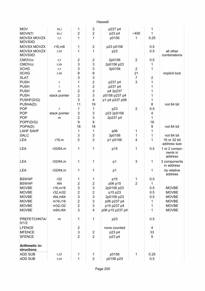
Haswell
Page 200
MOV m,i 1 2 p237 p4 1MOVNTI m,r 2 2 p23 p4 ~400 1
r,r 1 1 p0156 1 0.25
MOVSX MOVZX r16,m8 1 2 p23 p0156 0.5r,m 1 1 p23 0.5
CMOVcc r,r 2 2 2p0156 2 0.5CMOVcc r,m 3 3 2p0156 p23 1XCHG r,r 3 3 3p0156 2 1XCHG r,m 8 8 21 implicit lockXLAT 3 3 7 2PUSH r 1 2 p237 p4 3 1PUSH i 1 2 p237 p4 1PUSH m 2 3 p4 2p237 1PUSH stack pointer 2 3 p0156 p237 p4 1PUSHF(D/Q) 3 4 p1 p4 p237 p06 1PUSHA(D) 11 19 8 not 64 bitPOP r 1 1 p23 2 0.5POP stack pointer 3 3 p23 2p0156 4POP m 2 3 2p237 p4 1POPF(D/Q) 9 9 18POPA(D) 18 18 9 not 64 bitLAHF SAHF 1 1 p06 1 1SALC 3 3 3p0156 1 1 not 64 bitLEA r16,m 2 2 p1 p0156 4 1
LEA r32/64,m 1 1 p15 1 0.5
LEA r32/64,m 1 1 p1 3 1
LEA r32/64,m 1 1 p1 1
BSWAP r32 1 1 p15 1 0.5BSWAP r64 2 2 p06 p15 2 1MOVBE r16,m16 3 3 2p0156 p23 0.5 MOVBEMOVBE r32,m32 2 2 p15 p23 0.5 MOVBEMOVBE r64,m64 3 3 2p0156 p23 0.5 MOVBEMOVBE m16,r16 2 3 p06 p237 p4 1 MOVBEMOVBE m32,r32 2 3 p15 p237 p4 1 MOVBEMOVBE m64,r64 3 4 p06 p15 p237 p4 1 MOVBE
m 1 1 p23 0.5
LFENCE 2 none counted 4MFENCE 3 2 p23 p4 33SFENCE 2 2 p23 p4 5
ADD SUB r,r/i 1 1 p0156 1 0.25ADD SUB r,m 1 2 p0156 p23 0.5
MOVSX MOVZX MOVSXD
MOVSX MOVZX MOVSXD
all othercombinations
16 or 32 bit address size
1 or 2 compo-nents inaddress
3 components in address
rip relativeaddress
PREFETCHNTA/0/1/2
Arithmetic in-structions

Haswell
Page 201
ADD SUB m,r/i 2 4 2p0156 2p237 p4 6 1
ADC SBB r,r/i 2 2 2p0156 2 1ADC SBB r,m 2 3 2p0156 p23 1ADC SBB m,r/i 4 6 3p0156 2p237 p4 7 2
CMP r,r/i 1 1 p0156 1 0.25CMP m,r/i 1 2 p0156 p23 1 0.5
r 1 1 p0156 1 0.25
INC DEC NOT m 3 4 p0156 2p237 p4 6 1NEG m 2 4 p0156 2p237 p4 6 1AAA 2 2 p1 p0156 4 not 64 bitAAS 2 2 p1 p56 6 not 64 bitDAA DAS 3 3 p1 2p0156 4 not 64 bitAAD 3 3 p1 2p0156 4 not 64 bitAAM 8 8 p0 p1 p5 p6 21 8 not 64 bitMUL IMUL r8 1 1 p1 3 1MUL IMUL r16 4 4 p1 p0156 4 2MUL IMUL r32 3 3 p1 p0156 4 2MUL IMUL r64 2 2 p1 p6 3 1MUL IMUL m8 1 2 p1 p23 1MUL IMUL m16 4 5 p1 3p0156 p23 2MUL IMUL m32 3 4 p1 2p0156 p23 2MUL IMUL m64 2 3 p1 p6 p23 1IMUL r,r 1 1 p1 3 1IMUL r,m 1 2 p1 p23 1IMUL r16,r16,i 2 2 p1 p0156 4 1IMUL r32,r32,i 1 1 p1 3 1IMUL r64,r64,i 1 1 p1 3 1IMUL r16,m16,i 2 3 p1 p0156 p23 1IMUL r32,m32,i 1 2 p1 p23 1IMUL r64,m64,i 1 2 p1 p23 1MULX r32,r32,r32 3 3 p1 2p056 4 1 BMI2MULX r32,r32,m32 3 4 p1 2p056 p23 1 BMI2MULX r64,r64,r64 2 2 p1 p6 4 1 BMI2MULX r64,r64,m64 2 3 p1 p6 p23 1 BMI2DIV r8 9 9 p0 p1 p5 p6 22-25 9DIV r16 11 11 p0 p1 p5 p6 23-26 9DIV r32 10 10 p0 p1 p5 p6 22-29 9-11DIV r64 36 36 p0 p1 p5 p6 32-96 21-74IDIV r8 9 9 p0 p1 p5 p6 23-26 8IDIV r16 10 10 p0 p1 p5 p6 23-26 8IDIV r32 9 9 p0 p1 p5 p6 22-29 8-11IDIV r64 59 59 p0 p1 p5 p6 39-103 24-81CBW 1 1 p0156 1CWDE 1 1 p0156 1CDQE 1 1 p0156 1CWD 2 2 p0156 1CDQ 1 1 p06 1CQO 1 1 p06 1POPCNT r,r 1 1 p1 3 1 SSE4.2POPCNT r,m 1 2 p1 p23 1 SSE4.2
INC DEC NEG NOT

Haswell
Page 202
CRC32 r,r 1 1 p1 3 1 SSE4.2CRC32 r,m 1 2 p1 p23 1 SSE4.2
AND OR XOR r,r/i 1 1 p0156 1 0.25AND OR XOR r,m 1 2 p0156 p23 0.5AND OR XOR m,r/i 2 4 2p0156 2p237 p4 6 1
TEST r,r/i 1 1 p0156 1 0.25TEST m,r/i 1 2 p0156 p23 0.5SHR SHL SAR r,i 1 1 p06 1 0.5SHR SHL SAR m,i 3 4 2p06 p237 p4 2SHR SHL SAR r,cl 3 3 3p06 2 2SHR SHL SAR m,cl 5 6 3p06 2p23 p4 4ROR ROL r,1 2 2 2p06 1 1 short formROR ROL r,i 1 1 p06 1 0.5ROR ROL m,i 4 5 2p06 2p237 p4 2ROR ROL r,cl 3 3 3p06 2 2ROR ROL m,cl 5 6 4RCR RCL r,1 3 3 2p06 p0156 2 2RCR RCL m,1 4 6 3RCR RCL r,i 8 8 p0156 6 6RCR RCL m,i 11 11 6RCR RCL r,cl 8 8 p0156 6 6RCR RCL m,cl 11 11 6SHRD SHLD r,r,i 1 1 p1 3 1SHRD SHLD m,r,i 3 5 2SHLD r,r,cl 4 4 p0156 3 2SHRD r,r,cl 4 4 p0156 4 2SHRD SHLD m,r,cl 5 7 4SHLX SHRX SARX r,r,r 1 1 p06 1 0.5 BMI2SHLX SHRX SARX r,m,r 2 2 p06 p23 0.5 BMI2RORX r,r,i 1 1 p06 1 0.5 BMI2RORX r,m,i 2 2 p06 p23 0.5 BMI2BT r,r/i 1 1 p06 1 0.5BT m,r 10 10 5BT m,i 2 2 p06 p23 0.5BTR BTS BTC r,r/i 1 1 p06 1 0.5BTR BTS BTC m,r 10 11 5BTR BTS BTC m,i 3 4 2p06 p23 p4 2BSF BSR r,r 1 1 p1 3 1BSF BSR r,m 1 2 p1 p23 1SETcc r 1 1 p06 1 0.5SETcc m 2 3 p06 p237 p4 1CLC 1 0 none 0.25STC 1 1 p0156 0.25CMC 1 1 p0156 1CLD STD 3 3 p15 p6 4LZCNT r,r 1 1 p1 3 1 LZCNTLZCNT r,m 1 2 p1 p23 1 LZCNTTZCNT r,r 1 1 p1 3 1 BMI1TZCNT r,m 1 2 p1 p23 1 BMI1
Logic instruc-tions

Haswell
Page 203
ANDN r,r,r 1 1 p15 1 0.5 BMI1ANDN r,r,m 1 2 p15 p23 1 0.5 BMI1
r,r 1 1 p15 1 0.5 BMI1
r,m 1 2 p15 p23 0.5 BMI1
BEXTR r,r,r 2 2 2p0156 2 0.5 BMI1BEXTR r,m,r 3 3 2p0156 p23 1 BMI1BZHI r,r,r 1 1 p15 1 0.5 BMI2BZHI r,m,r 1 2 p15 p23 0.5 BMI2PDEP r,r,r 1 1 p1 3 1 BMI2PDEP r,r,m 1 2 p1 p23 1 BMI2PEXT r,r,r 1 1 p1 3 1 BMI2PEXT r,r,m 1 2 p1 p23 1 BMI2
Control transfer instructionsJMP short/near 1 1 p6 1-2JMP r 1 1 p6 2JMP m 1 2 p23 p6 2Conditional jump short/near 1 1 p6 1-2
Conditional jump short/near 1 1 p06 0.5-1
1 1 p6 1-2
1 1 p06 0.5-1
J(E/R)CXZ short 2 2 p0156 p6 0.5-2LOOP short 7 7 5LOOP(N)E short 11 11 6CALL near 2 3 p237 p4 p6 2CALL r 2 3 p237 p4 p6 2CALL m 3 4 2p237 p4 p6 3RET 1 2 p237 p6 1RET i 3 4 p23 2p6 p015 2BOUND r,m 15 15 8 not 64 bitINTO 4 4 5 not 64 bit
LODSB/W 3 3 2p0156 p23 1LODSD/Q 2 2 p0156 p23 1REP LODS 5n+12 ~2nSTOS 3 3 p23 p0156 p4 1REP STOS <2n ~0.5n worst caseREP STOS 2.6/32B 1/32B
MOVS 5 5 2p23 p4 2p0156 4REP MOVS ~2n ~1.5 n worst caseREP MOVS 4/32B 1/32B
SCAS 3 3 p23 2p0156 1REP SCAS ≥6n ≥2n
BLSI BLSMSK BLSR
BLSI BLSMSK BLSR
predicted taken
predicted not taken
Fused arithmetic and branch
predicted taken
Fused arithmetic and branch
predicted not taken
String instruc-tions
best casealigned by 32
best casealigned by 32

Haswell
Page 204
CMPS 5 5 2p23 3p0156 4REP CMPS ≥8n ≥2n
Synchronization instructionsXADD m,r 4 5 7LOCK XADD m,r 9 9 19LOCK ADD m,r 8 8 19CMPXCHG m,r 5 6 8LOCK CMPXCHG m,r 10 10 19CMPXCHG8B m,r 15 15 9LOCK CMPXCHG8B m,r 19 19 19CMPXCHG16B m,r 22 22 15LOCK CMPXCHG16B m,r 24 24 25
OtherNOP (90) 1 0 none 0.25
1 0 none 0.25
PAUSE 5 5 p05 3p6 9ENTER a,0 12 12 8ENTER a,b ~14+7b ~45+7b ~87+2bLEAVE 3 3 2p0156 p23 6XGETBV 8 8 9 XGETBVRDTSC 15 15 24RDPMC 34 34 37RDRAND r 17 17 p23 16p0156 ~320 RDRAND
Floating point x87 instructions
Instruction Operands µops each port Latency Comments
FLD r 1 1 p01 1 0.5FLD m32/64 1 1 p23 3 0.5FLD m80 4 4 2p01 2p23 4 2FBLD m80 43 43 47 22FST(P) r 1 1 p01 1 0.5FST(P) m32/m64 1 2 p4 p237 4 1FSTP m80 7 7 3p0156 2p23 2p4 1 5FBSTP m80 238 226 265FXCH r 2 0 none 0 0.5FILD m 1 2 p01 p23 6 1FIST(P) m 3 3 p1 p23 p4 7 1FISTTP m 3 3 p1 p23 p4 7 2 SSE3FLDZ 1 1 p01 1FLD1 2 2 2p01 2FLDPI FLDL2E etc. 2 2 2p01 2FCMOVcc r 3 3 2p0 p5 2 2FNSTSW AX 2 2 p0 p0156 1FNSTSW m16 2 3 p0 p4 p237 6 1FLDCW m16 3 3 p01 p23 p6 7 2
Long NOP (0F 1F)
µops fused domain
µops unfused domain
Recipro-cal throughput
Move instruc-tions

Haswell
Page 205
FNSTCW m16 2 3 p237 p4 p6 1FINCSTP FDECSTP 1 1 p01 0 0.5FFREE(P) r 1 1 p01 0.5FNSAVE m 147 147 150FRSTOR m 90 90 164
r 1 1 p1 3 1
m 1 2 p1 p23 1FMUL(P) r 1 1 p0 5 1FMUL(P) m 1 2 p0 p23 1FDIV(R)(P) r 1 1 p0 10-24 8-18FDIV(R)(P) m 1 2 p0 p23 8-18FABS 1 1 p0 1 1FCHS 1 1 p0 1 1FCOM(P) FUCOM r 1 1 p1 1FCOM(P) FUCOM m 1 2 p1 p23 1FCOMPP FUCOMPP 2 2 2p01 1FCOMI(P) FUCOMI r 3 3 3p01 1.5FIADD FISUB(R) m 2 3 2p1 p23 2FIMUL m 2 3 p0 p1 p23 2FIDIV(R) m 2 3 p0 p1 p23FICOM(P) m 2 3 2p1 p23 2FTST 1 1 p1 1FXAM 2 2 2p1 2FPREM 28 28 19 13FPREM1 41 41 27 17FRNDINT 17 17 11 23
MathFSCALE 25-75 49-125FXTRACT 17 17 15 11FSQRT 1 1 p0 10-23 8-17FSIN 71-100 47-106FCOS 110 112FSINCOS 70-120 52-123F2XM1 58-89 63-68FYL2X 55-417 58-680FYL2XP1 55-228 58-360FPTAN 110-121 130FPATAN 78-160 96-156
OtherFNOP 1 1 p01 0.5WAIT 2 2 p01 1FNCLEX 5 5 p0156 22FNINIT 26 26 83
Integer vector instructions
Arithmetic in-structions
FADD(P)FSUB(R)(P)
FADD(P)FSUB(R)(P)

Haswell
Page 206
Instruction Operands µops each port Latency Comments
MOVD r32/64,(x)mm 1 1 p0 1 1MOVD m32/64,(x)mm 1 2 p237 p4 3 1MOVD (x)mm,r32/64 1 1 p5 1 1MOVD (x)mm,m32/64 1 1 p23 3 0.5MOVQ r64,(x)mm 1 1 p0 1 1MOVQ (x)mm,r64 1 1 p5 1 1MOVQ (x)mm,(x)mm 1 p015 1 0.33MOVQ (x)mm,m64 1 1 p23 3 0.5MOVQ m64, (x)mm 1 2 p237 p4 3 1MOVDQA/U x,x 1 1 p015 0-1 0.33 may be elim.MOVDQA/U x, m128 1 1 p23 3 0.5MOVDQA/U m128, x 1 2 p237 p4 3 1
VMOVDQA/U y,y 1 1 p015 0-1 0.33VMOVDQA/U y,m256 1 1 p23 3 0.5 AVXVMOVDQA/U m256,y 1 2 p237 p4 4 1 AVXLDDQU x, m128 1 1 p23 3 0.5 SSE3MOVDQ2Q mm, x 2 2 p01 p5 1 1MOVQ2DQ x,mm 1 1 p015 1 0.33MOVNTQ m64,mm 1 2 p237 p4 ~400 1MOVNTDQ m128,x 1 2 p237 p4 ~400 1VMOVNTDQ m256,y 1 2 p237 p4 ~400 1 AVX2MOVNTDQA x, m128 1 1 p23 3 0.5 SSE4.1VMOVNTDQA y,m256 1 1 p23 3 0.5 AVX2
mm,mm 3 3 p5 2 2
mm,m64 3 3 p23 2p5 2
x,x / y,y,y 1 1 p5 1 1
x,m / y,y,m 1 2 p23 p5 1PACKUSDW x,x / y,y,y 1 1 p5 1 1 SSE4.1PACKUSDW x,m / y,y,m 1 2 p23 p5 1 SSE4.1
v,v / v,v,v 1 1 p5 1 1
v,m / v,v,m 1 2 p23 p5 1
x,x / y,y,y 1 1 p5 1 1
x,m / y,y,m 2 2 p23 p5 1
x,x 1 1 p5 1 1 SSE4.1
x,m 1 2 p23 p5 1 SSE4.1
y,x 1 1 p5 3 1 AVX2
µops fused domain
µops unfused domain
Recipro-cal throughput
Move instruc-tions
AVXmay be elim.
PACKSSWB/DW PACKUSWB
PACKSSWB/DW PACKUSWB
PACKSSWB/DW PACKUSWB
PACKSSWB/DW PACKUSWB
PUNPCKH/LBW/WD/DQ
PUNPCKH/LBW/WD/DQ
PUNPCKH/LQDQ
PUNPCKH/LQDQ
PMOVSX/ZX BW BD BQ DW DQ
PMOVSX/ZX BW BD BQ DW DQ
VPMOVSX/ZX BW BD BQ DW DQ

Haswell
Page 207
y,m 2 2 p5 p23 1 AVX2PSHUFB v,v / v,v,v 1 1 p5 1 1 SSSE3PSHUFB v,m / v,v,m 2 2 p23 p5 1 SSSE3PSHUFW mm,mm,i 1 1 p5 1 1PSHUFW mm,m64,i 2 2 p23 p5 1PSHUFD v,v,i 1 1 p5 1 1PSHUFD v,m,i 2 2 p23 p5 1PSHUFL/HW v,v,i 1 1 p5 1 1PSHUFL/HW v,m,i 2 2 p23 p5 1PALIGNR v,v,i / v,v,v,i 1 1 p5 1 1 SSSE3PALIGNR v,m,i / v,v,m,i 2 2 p23 p5 1 SSSE3PBLENDVB x,x,xmm0 2 2 2p5 2 2 SSE4.1PBLENDVB x,m,xmm0 3 3 2p5 p23 2 SSE4.1VPBLENDVB v,v,v,v 2 2 2p5 2 2 AVX2VPBLENDVB v,v,m,v 3 3 2p5 p23 2 AVX2PBLENDW x,x,i / v,v,v,i 1 1 p5 1 1 SSE4.1PBLENDW x,m,i / v,v,m,i 2 2 p23 p5 1 SSE4.1VPBLENDD v,v,v,i 1 1 p015 1 0.33 AVX2VPBLENDD v,v,m,i 2 2 p015 p23 0.5 AVX2VPERMD y,y,y 1 1 p5 3 1 AVX2VPERMD y,y,m 1 2 p5 p23 1 AVX2VPERMQ y,y,i 1 1 p5 3 1 AVX2VPERMQ y,m,i 2 2 p5 p23 1 AVX2VPERM2I128 y,y,y,i 1 1 p5 3 1 AVX2VPERM2I128 y,y,m,i 2 2 p5 p23 1 AVX2MASKMOVQ mm,mm 4 4 p0 p4 2p23 13-413 1MASKMOVDQU x,x 10 10 4p04 2p56 4p23 14-438 6VPMASKMOVD/Q v,v,m 3 3 p23 2p5 4 2 AVX2VPMASKMOVD/Q m,v,v 4 4 p0 p1 p4 p23 13-14 1 AVX2PMOVMSKB r,v 1 1 p0 3 1PEXTRB/W/D/Q r32,x,i 2 2 p0 p5 2 1 SSE4.1PEXTRB/W/D/Q m8,x,i 2 3 p23 p4 p5 1 SSE4.1VEXTRACTI128 x,y,i 1 1 p5 3 1 AVX2VEXTRACTI128 m,y,i 2 2 p23 p4 4 1 AVX2PINSRB x,r32,i 2 2 p5 2 2 SSE4.1PINSRB x,m8,i 2 2 p23 p5 1 SSE4.1PINSRW (x)mm,r32,i 2 2 p5 2 2PINSRW (x)mm,m16,i 2 2 p23 p5 1PINSRD/Q x,r32,i 2 2 p5 2 2 SSE4.1PINSRD/Q x,m32,i 2 2 p23 p5 1 SSE4.1VINSERTI128 y,y,x,i 1 1 p5 3 1 AVX2VINSERTI128 y,y,m,i 2 2 p015 p23 4 0.5 AVX2
x,x 1 1 p5 1 1 AVX2
x,m8/16 3 3 p01 p23 p5 5 1 AVX2
x,m32/64 1 1 p23 4 0.5 AVX2
y,x 1 1 p5 3 1 AVX2
y,m8/16 3 3 p01 p23 p5 7 1 AVX2
VPMOVSX/ZX BW BD BQ DW DQ
VPBROADCASTB/W/D/Q
VPBROADCASTB/W
VPBROADCASTD/Q
VPBROADCASTB/W/D/Q
VPBROADCASTB/W

Haswell
Page 208
y,m32/64 1 1 p23 5 0.5 AVX2VBROADCASTI128 y,m128 1 1 p23 3 0.5 AVX2VPGATHERDD x,[r+s*x],x 20 20 9 AVX2VPGATHERDD y,[r+s*y],y 34 34 12 AVX2VPGATHERQD x,[r+s*x],x 15 15 8 AVX2VPGATHERQD x,[r+s*y],x 22 22 7 AVX2VPGATHERDQ x,[r+s*x],x 12 12 7 AVX2VPGATHERDQ y,[r+s*x],y 20 20 9 AVX2VPGATHERQQ x,[r+s*x],x 14 14 7 AVX2VPGATHERQQ y,[r+s*y],y 22 22 9 AVX2
v,v / v,v,v 1 1 p15 1 0.5
v,m / v,v,m 1 2 p15 p23 0.5
v,v / v,v,v 3 3 p1 2p5 3 2 SSSE3
v,m / v,v,m 4 4 p1 2p5 p23 2 SSSE3
v,v / v,v,v 1 1 p15 1 0.5
v,m / v,v,m 1 2 p15 p23 0.5PCMPEQQ v,v / v,v,v 1 1 p15 1 0.5 SSE4.1PCMPEQQ v,m / v,v,m 1 2 p15 p23 0.5 SSE4.1PCMPGTQ v,v / v,v,v 1 1 p0 5 1 SSE4.2PCMPGTQ v,m / v,v,m 1 2 p0 p23 1 SSE4.2
v,v / v,v,v 1 1 p0 5 1
v,m / v,v,m 1 2 p0 p23 1PMULHRSW v,v / v,v,v 1 1 p0 5 1 SSSE3PMULHRSW v,m / v,v,m 1 2 p0 p23 1 SSSE3PMULLD x,x / y,y,y 2 2 2p0 10 2 SSE4.1PMULLD x,m / y,y,m 3 3 2p0 p23 2 SSE4.1PMULDQ x,x / y,y,y 1 1 p0 5 1 SSE4.1PMULDQ x,m / y,y,m 1 2 p0 p23 1 SSE4.1PMULUDQ v,v / v,v,v 1 1 p0 5 1PMULUDQ v,m / v,v,m 1 2 p0 p23 1PMADDWD v,v / v,v,v 1 1 p0 5 1PMADDWD v,m / v,v,m 1 2 p0 p23 1PMADDUBSW v,v / v,v,v 1 1 p0 5 1 SSSE3PMADDUBSW v,m / v,v,m 1 2 p0 p23 1 SSSE3PAVGB/W v,v / v,v,v 1 1 p15 1 0.5PAVGB/W v,m / v,v,m 1 2 p15 p23 0.5
x,x / y,y,y 1 1 p15 1 0.5 SSE4.1
x,m / y,y,m 1 2 p15 p23 0.5 SSE4.1
VPBROADCASTD/Q
Arithmetic in-structionsPADD/SUB(S,US) B/W/D/Q
PADD/SUB(S,US) B/W/D/Q
PHADD(S)W/DPHSUB(S)W/D
PHADD(S)W/DPHSUB(S)W/D
PCMPEQB/W/DPCMPGTB/W/D
PCMPEQB/W/DPCMPGTB/W/D
PMULL/HWPMULHUW
PMULL/HWPMULHUW
PMIN/PMAXSB/SW/SDUB/UW/UD
PMIN/PMAXSB/SW/SDUB/UW/UD
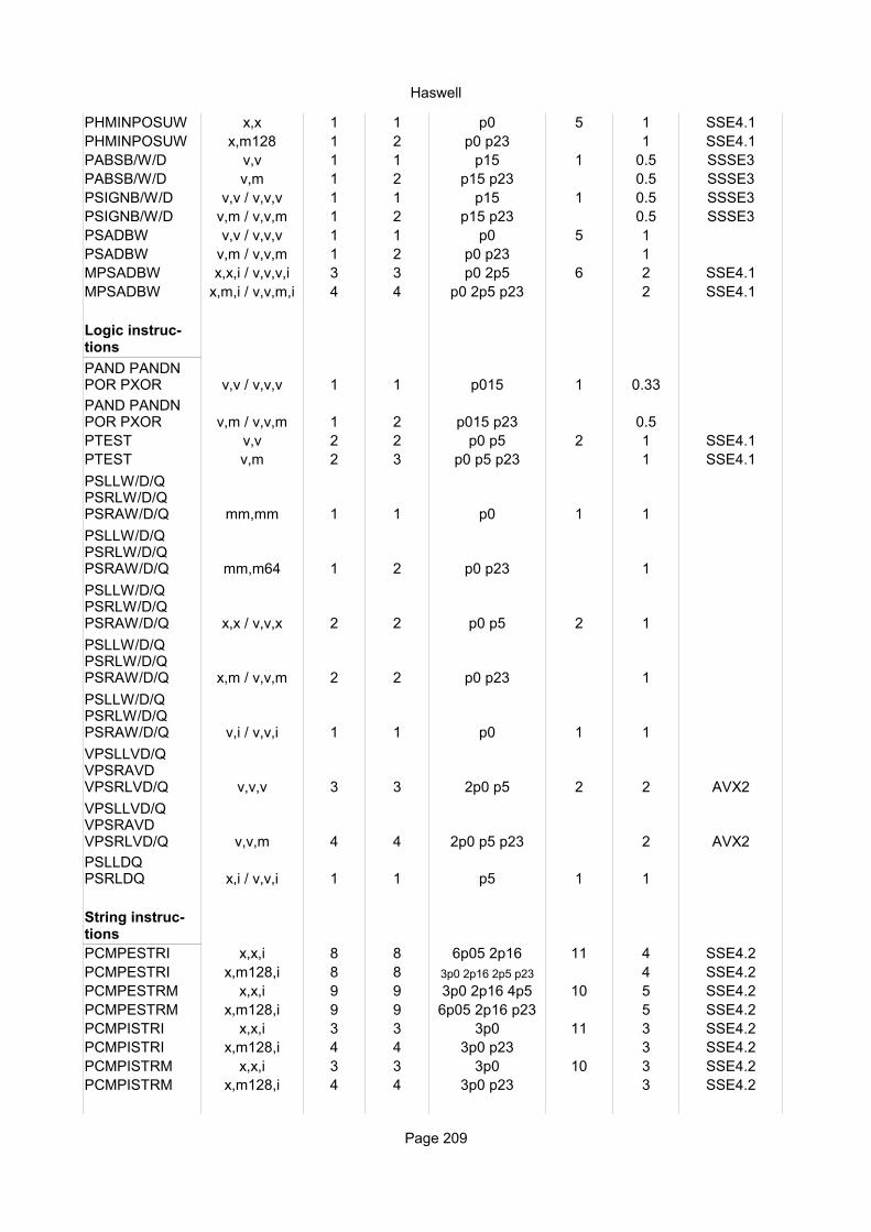
Haswell
Page 209
PHMINPOSUW x,x 1 1 p0 5 1 SSE4.1PHMINPOSUW x,m128 1 2 p0 p23 1 SSE4.1PABSB/W/D v,v 1 1 p15 1 0.5 SSSE3PABSB/W/D v,m 1 2 p15 p23 0.5 SSSE3PSIGNB/W/D v,v / v,v,v 1 1 p15 1 0.5 SSSE3PSIGNB/W/D v,m / v,v,m 1 2 p15 p23 0.5 SSSE3PSADBW v,v / v,v,v 1 1 p0 5 1PSADBW v,m / v,v,m 1 2 p0 p23 1MPSADBW x,x,i / v,v,v,i 3 3 p0 2p5 6 2 SSE4.1MPSADBW x,m,i / v,v,m,i 4 4 p0 2p5 p23 2 SSE4.1
v,v / v,v,v 1 1 p015 1 0.33
v,m / v,v,m 1 2 p015 p23 0.5PTEST v,v 2 2 p0 p5 2 1 SSE4.1PTEST v,m 2 3 p0 p5 p23 1 SSE4.1
mm,mm 1 1 p0 1 1
mm,m64 1 2 p0 p23 1
x,x / v,v,x 2 2 p0 p5 2 1
x,m / v,v,m 2 2 p0 p23 1
v,i / v,v,i 1 1 p0 1 1
v,v,v 3 3 2p0 p5 2 2 AVX2
v,v,m 4 4 2p0 p5 p23 2 AVX2
x,i / v,v,i 1 1 p5 1 1
PCMPESTRI x,x,i 8 8 6p05 2p16 11 4 SSE4.2PCMPESTRI x,m128,i 8 8 3p0 2p16 2p5 p23 4 SSE4.2PCMPESTRM x,x,i 9 9 3p0 2p16 4p5 10 5 SSE4.2PCMPESTRM x,m128,i 9 9 6p05 2p16 p23 5 SSE4.2PCMPISTRI x,x,i 3 3 3p0 11 3 SSE4.2PCMPISTRI x,m128,i 4 4 3p0 p23 3 SSE4.2PCMPISTRM x,x,i 3 3 3p0 10 3 SSE4.2PCMPISTRM x,m128,i 4 4 3p0 p23 3 SSE4.2
Logic instruc-tions
PAND PANDNPOR PXOR
PAND PANDNPOR PXOR
PSLLW/D/QPSRLW/D/QPSRAW/D/Q
PSLLW/D/QPSRLW/D/QPSRAW/D/Q
PSLLW/D/QPSRLW/D/QPSRAW/D/Q
PSLLW/D/QPSRLW/D/QPSRAW/D/Q
PSLLW/D/QPSRLW/D/QPSRAW/D/Q
VPSLLVD/QVPSRAVDVPSRLVD/Q
VPSLLVD/QVPSRAVDVPSRLVD/Q
PSLLDQPSRLDQ
String instruc-tions
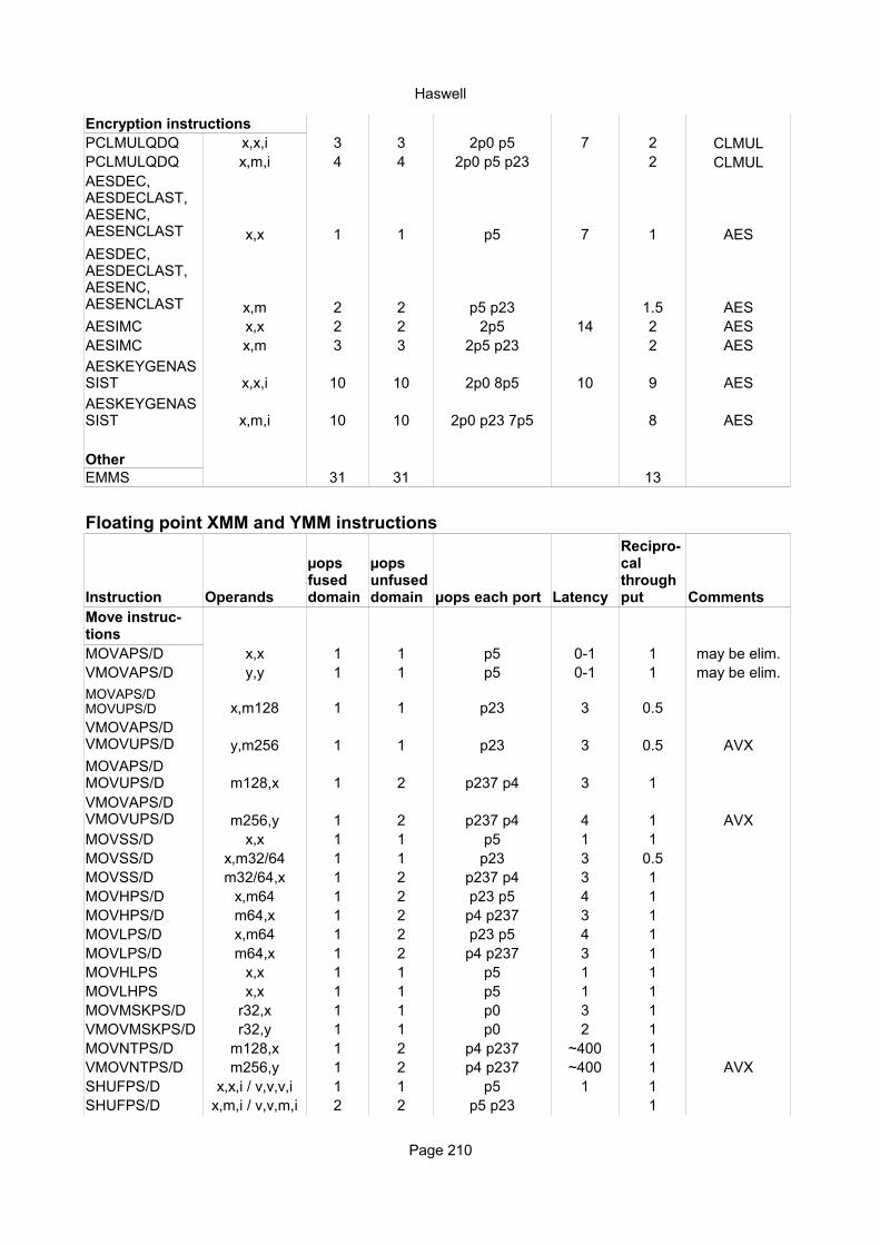
Haswell
Page 210
Encryption instructionsPCLMULQDQ x,x,i 3 3 2p0 p5 7 2 CLMULPCLMULQDQ x,m,i 4 4 2p0 p5 p23 2 CLMUL
x,x 1 1 p5 7 1 AES
x,m 2 2 p5 p23 1.5 AESAESIMC x,x 2 2 2p5 14 2 AESAESIMC x,m 3 3 2p5 p23 2 AES
x,x,i 10 10 2p0 8p5 10 9 AES
x,m,i 10 10 2p0 p23 7p5 8 AES
OtherEMMS 31 31 13
Floating point XMM and YMM instructions
Instruction Operands µops each port Latency Comments
MOVAPS/D x,x 1 1 p5 0-1 1 may be elim.VMOVAPS/D y,y 1 1 p5 0-1 1 may be elim.
x,m128 1 1 p23 3 0.5
y,m256 1 1 p23 3 0.5 AVX
m128,x 1 2 p237 p4 3 1
m256,y 1 2 p237 p4 4 1 AVXMOVSS/D x,x 1 1 p5 1 1MOVSS/D x,m32/64 1 1 p23 3 0.5MOVSS/D m32/64,x 1 2 p237 p4 3 1MOVHPS/D x,m64 1 2 p23 p5 4 1MOVHPS/D m64,x 1 2 p4 p237 3 1MOVLPS/D x,m64 1 2 p23 p5 4 1MOVLPS/D m64,x 1 2 p4 p237 3 1MOVHLPS x,x 1 1 p5 1 1MOVLHPS x,x 1 1 p5 1 1MOVMSKPS/D r32,x 1 1 p0 3 1VMOVMSKPS/D r32,y 1 1 p0 2 1MOVNTPS/D m128,x 1 2 p4 p237 ~400 1VMOVNTPS/D m256,y 1 2 p4 p237 ~400 1 AVXSHUFPS/D x,x,i / v,v,v,i 1 1 p5 1 1SHUFPS/D x,m,i / v,v,m,i 2 2 p5 p23 1
AESDEC, AESDECLAST, AESENC, AESENCLAST
AESDEC, AESDECLAST, AESENC, AESENCLAST
AESKEYGENASSIST
AESKEYGENASSIST
µops fused domain
µops unfused domain
Recipro-cal throughput
Move instruc-tions
MOVAPS/DMOVUPS/D
VMOVAPS/D VMOVUPS/D
MOVAPS/DMOVUPS/DVMOVAPS/D VMOVUPS/D

Haswell
Page 211
VPERMILPS/PD v,v,i 1 1 p5 1 1 AVXVPERMILPS/PD v,m,i 2 2 p5 p23 1 AVXVPERMILPS/PD v,v,v 1 1 p5 1 1 AVXVPERMILPS/PD v,v,m 2 2 p5 p23 1 AVXVPERM2F128 y,y,y,i 1 1 p5 3 1 AVXVPERM2F128 y,y,m,i 2 2 p5 p23 1 AVXVPERMPS y,y,y 1 1 p5 3 1 AVX2VPERMPS y,y,m 1 2 p5 p23 1 AVX2VPERMPD y,y,i 1 1 p5 3 1 AVX2VPERMPD y,m,i 2 2 p5 p23 1 AVX2BLENDPS/PD x,x,i / v,v,v,i 1 1 p015 1 0.33 SSE4.1BLENDPS/PD x,m,i / v,v,m,i 2 2 p015 p23 0.5 SSE4.1BLENDVPS/PD x,x,xmm0 2 2 2p5 2 2 SSE4.1BLENDVPS/PD x,m,xmm0 3 3 2p5 p23 2 SSE4.1VBLENDVPS/PD v,v,v,v 2 2 2p5 2 2 AVXVBLENDVPS/PD v,v,m,v 3 3 2p5 p23 2 AVXMOVDDUP v,v 1 1 p5 1 1 SSE3MOVDDUP v,m 1 1 p23 3 0.5 SSE3VBROADCASTSS x,m32 1 1 p23 4 0.5 AVXVBROADCASTSS y,m32 1 1 p23 5 0.5 AVXVBROADCASTSS x,x 1 1 p5 1 1 AVX2VBROADCASTSS y,x 1 1 p5 3 1 AVX2VBROADCASTSD y,m64 1 1 p23 5 0.5 AVXVBROADCASTSD y,x 1 1 p5 3 1 AVX2VBROADCASTF128 y,m128 1 1 p23 3 0.5 AVXMOVSH/LDUP v,v 1 1 p5 1 1 SSE3MOVSH/LDUP v,m 1 1 p23 3 0.5 SSE3UNPCKH/LPS/D x,x / v,v,v 1 1 p5 1 1 SSE3UNPCKH/LPS/D x,m / v,v,m 1 2 p5 p23 1 SSE3EXTRACTPS r32,x,i 2 2 p0 p5 1 SSE4.1EXTRACTPS m32,x,i 3 3 p0 p5 p23 4 1 SSE4.1VEXTRACTF128 x,y,i 1 1 p5 3 1 AVXVEXTRACTF128 m128,y,i 2 2 p23 p4 4 1 AVXINSERTPS x,x,i 1 1 p5 1 1 SSE4.1INSERTPS x,m32,i 2 2 p23 p5 4 1 SSE4.1VINSERTF128 y,y,x,i 1 1 p5 3 1 AVXVINSERTF128 y,y,m128,i 2 2 p015 p23 4 2 AVXVMASKMOVPS/D v,v,m 3 3 2p5 p23 4 2 AVXVMASKMOVPS/D m128,x,x 4 4 p0 p1 p4 p23 13 1 AVXVMASKMOVPS/D m256,y,y 4 4 p0 p1 p4 p23 14 2 AVXVGATHERDPS x,[r+s*x],x 20 20 9 AVX2VGATHERDPS y,[r+s*y],y 34 34 12 AVX2VGATHERQPS x,[r+s*x],x 15 15 8 AVX2VGATHERQPS x,[r+s*y],x 22 22 7 AVX2VGATHERDPD x,[r+s*x],x 12 12 7 AVX2VGATHERDPD y,[r+s*x],y 20 20 9 AVX2VGATHERQPD x,[r+s*x],x 14 14 7 AVX2VGATHERQPD y,[r+s*y],y 22 22 9 AVX2
ConversionCVTPD2PS x,x 2 2 p1 p5 4 1CVTPD2PS x,m128 2 3 p1 p5 p23 1VCVTPD2PS x,y 2 2 p1 p5 5 1 AVX

Haswell
Page 212
VCVTPD2PS x,m256 2 3 p1 p5 p23 1 AVXCVTSD2SS x,x 2 2 p1 p5 4 1CVTSD2SS x,m64 2 3 p1 p5 p23 1CVTPS2PD x,x 2 2 p0 p5 2 1CVTPS2PD x,m64 2 2 p0 p23 1VCVTPS2PD y,x 2 2 p0 p5 5 1 AVXVCVTPS2PD y,m128 2 2 p0 p23 1 AVXCVTSS2SD x,x 2 2 p0 p5 2 1CVTSS2SD x,m32 2 2 p0 p23 1CVTDQ2PS x,x 1 1 p1 3 1CVTDQ2PS x,m128 1 2 p1 p23 1VCVTDQ2PS y,y 1 1 p1 3 1 AVXVCVTDQ2PS y,m256 1 2 p1 p23 1 AVXCVT(T) PS2DQ x,x 1 1 p1 3 1CVT(T) PS2DQ x,m128 1 2 p1 p23 1VCVT(T) PS2DQ y,y 1 1 p1 3 1 AVXVCVT(T) PS2DQ y,m256 1 2 p1 p23 1 AVXCVTDQ2PD x,x 2 2 p1 p5 4 1CVTDQ2PD x,m64 2 2 p1 p23 1VCVTDQ2PD y,x 2 2 p1 p5 6 1 AVXVCVTDQ2PD y,m128 2 2 p1 p23 1 AVXCVT(T)PD2DQ x,x 2 2 p1 p5 4 1CVT(T)PD2DQ x,m128 2 3 p1 p5 p23 1VCVT(T)PD2DQ x,y 2 2 p1 p5 6 1 AVXVCVT(T)PD2DQ x,m256 2 3 p1 p5 p23 1 AVXCVTPI2PS x,mm 1 1 p1 4 4CVTPI2PS x,m64 1 2 p1 p23 3CVT(T)PS2PI mm,x 2 2 p1 p5 4 1CVT(T)PS2PI mm,m128 2 2 p1 p23 1CVTPI2PD x,mm 2 2 p1 p5 4 1CVTPI2PD x,m64 2 2 p1 p23 1CVT(T) PD2PI mm,x 2 2 p1 p5 4 1CVT(T) PD2PI mm,m128 2 3 p1 p5 p23 1CVTSI2SS x,r32 2 2 p1 p5 4 3CVTSI2SS x,m32 1 2 p1 p23 3CVT(T)SS2SI r32,x 2 2 p0 p1 4 1CVT(T)SS2SI r32,m32 2 3 p0 p1 p23 1CVTSI2SD x,r32/64 2 2 p1 p5 4 3CVTSI2SD x,m32 2 2 p1 p23 3CVT(T)SD2SI r32/64,x 2 2 p0 p1 4 1CVT(T)SD2SI r32,m64 2 3 p0 p1 p23 1VCVTPS2PH x,v,i 2 2 p1 p5 4 1 F16CVCVTPS2PH m,v,i 4 4 p1 p4 p5 p23 1 F16CVCVTPH2PS v,x 2 2 p1 p5 4 1 F16CVCVTPH2PS v,m 2 2 p1 p23 1 F16C
Arithmetic
x,x / v,v,v 1 1 p1 3 1
x,m / v,v,m 1 2 p1 p23 1ADDSUBPS/D x,x / v,v,v 1 1 p1 3 1 SSE3ADDSUBPS/D x,m / v,v,m 1 2 p1 p23 1 SSE3
ADDSS/D PS/DSUBSS/D PS/D
ADDSS/D PS/DSUBSS/D PS/D

Haswell
Page 213
x,x / v,v,v 3 3 p1 2p5 5 2 SSE3
x,m / v,v,m 4 4 p1 2p5 p23 2 SSE3MULSS/D PS/D x,x / v,v,v 1 1 p01 5 0.5MULSS/D PS/D x,m / v,v,m 1 2 p01 p23 0.5DIVSS DIVPS x,x 1 1 p0 10-13 7DIVSS DIVPS x,m 1 2 p0 p23 7DIVSD DIVPD x,x 1 1 p0 10-20 8-14DIVSD DIVPD x,m 1 2 p0 p23 8-14VDIVPS y,y,y 3 3 2p0 p15 18-21 14 AVXVDIVPS y,y,m256 4 4 2p0 p15 p23 14 AVXVDIVPD y,y,y 3 3 2p0 p15 19-35 16-28 AVXVDIVPD y,y,m256 4 4 2p0 p15 p23 16-28 AVXRCPSS/PS x,x 1 1 p0 5 1RCPSS/PS x,m128 1 2 p0 p23 1VRCPPS y,y 3 3 2p0 p15 7 2 AVXVRCPPS y,m256 4 4 2p0 p15 p23 2 AVX
x,x / v,v,v 1 1 p1 3 1
x,m / v,v,m 2 2 p1 p23 1(U)COMISS/D x,x 1 1 p1 1(U)COMISS/D x,m32/64 2 2 p1 p23 1
x,x / v,v,v 1 1 p1 3 1
x,m / v,v,m 1 2 p1 p23 1
ROUNDSS/D PS/D v,v,i 2 2 2p1 6 2 SSE4.1
ROUNDSS/D PS/D v,m,i 3 3 2p1 p23 2 SSE4.1DPPS x,x,i / v,v,v,i 4 4 2p0 p1 p5 14 2 SSE4.1DPPS x,m,i / v,v,m,i 6 6 2p0 p1 p5 p23 p6 4 SSE4.1DPPD x,x,i 3 3 p0 p1 p5 9 1 SSE4.1DPPD x,m128,i 4 4 p0 p1 p5 p23 1 SSE4.1
v,v,v 1 1 p01 5 0.5 FMA
v,v,m 1 2 p01 p23 0.5 FMA
MathSQRTSS/PS x,x 1 1 p0 11 7SQRTSS/PS x,m128 1 2 p0 p23 7VSQRTPS y,y 3 3 2p0 p15 19 14 AVXVSQRTPS y,m256 4 4 2p0 p15 p23 14 AVXSQRTSD/PD x,x 1 1 p0 16 8-14SQRTSD/PD x,m128 1 2 p0 p23 8-14VSQRTPD y,y 3 3 2p0 p15 28-29 16-28 AVXVSQRTPD y,m256 4 4 2p0 p15 p23 16-28 AVXRSQRTSS/PS x,x 1 1 p0 5 1RSQRTSS/PS x,m128 1 2 p0 p23 1VRSQRTPS y,y 3 3 2p0 p15 7 2 AVX
HADDPS/DHSUBPS/D
HADDPS/DHSUBPS/D
CMPccSS/D CMPccPS/D
CMPccSS/D CMPccPS/D
MAXSS/D PS/DMINSS/D PS/D
MAXSS/D PS/DMINSS/D PS/D
VFMADD...(all FMA instr.)
VFMADD...(all FMA instr.)
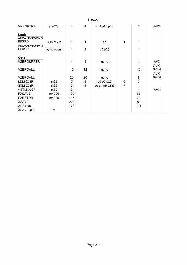
Haswell
Page 214
VRSQRTPS y,m256 4 4 2p0 p15 p23 2 AVX
Logic
x,x / v,v,v 1 1 p5 1 1
x,m / v,v,m 1 2 p5 p23 1
OtherVZEROUPPER 4 4 none 1 AVX
VZEROALL 12 12 none 10
VZEROALL 20 20 none 8LDMXCSR m32 3 3 p0 p6 p23 6 3STMXCSR m32 3 4 p0 p4 p6 p237 7 1VSTMXCSR m32 3 1 AVXFXSAVE m4096 130 68FXRSTOR m4096 116 72XSAVE 224 84XRSTOR 173 111XSAVEOPT m
AND/ANDN/OR/XORPS/PD
AND/ANDN/OR/XORPS/PD
AVX,32 bit
AVX,64 bit

Broadwell
Page 215
Intel BroadwellList of instruction timings and μop breakdown
Explanation of column headings:Instruction:
Operands:
µops each port:
Latency:
Integer instructions
Instruction Operands µops each port Latency Comments
MOV r,i 1 1 p0156 0.25MOV r8/16,r8/16 1 1 p0156 1 0.25MOV r32/64,r32/64 1 1 p0156 0-1 0.25 may be elim.MOV r8l,m 1 2 p23 p0156 0.5MOV r8h,m 1 1 p23 0.5MOV r16,m 1 2 p23 p0156 0.5MOV r32/64,m 1 1 p23 2 0.5
MOV m,r 1 2 p237 p4 3 1
Name of instruction. Multiple names mean that these instructions have the same data. Instructions with or without V name prefix behave the same unless otherwise noted.
i = immediate data, r = register, mm = 64 bit mmx register, x = 128 bit xmm register, (x)mm = mmx or xmm register, y = 256 bit ymm register, v = any vector register (mmx, xmm, ymm). same = same register for both operands. m = memory operand, m32 = 32-bit memory operand, etc.
μops fused domain:
The number of μops at the decode, rename and allocate stages in the pipeline. Fused μops count as one.
μops unfused domain:
The total number of μops for all execution port. Fused μops count as two. Fused macro-ops count as one. The instruction has μop fusion if this number is higher than the num-ber under fused domain. Some operations are not counted here if they do not go to any execution port or if the counters are inaccurate.
The number of μops for each execution port. p0 means a µop to execution port 0. p01means a µop that can go to either port 0 or port 1. p0 p1 means two µops going to port 0 and 1, respectively.Port 0: Integer, f.p. and vector ALU, mul, div, branchPort 1: Integer, f.p. and vector ALUPort 2: LoadPort 3: LoadPort 4: StorePort 5: Integer and vector ALUPort 6: Integer ALU, branchPort 7: Store address
This is the delay that the instruction generates in a dependency chain. The numbers are minimum values. Cache misses, misalignment, and exceptions may increase the clock counts considerably. Where hyperthreading is enabled, the use of the same execution units in the other thread leads to inferior performance. Denormal numbers, NAN's and in-finity do not increase the latency. The time unit used is core clock cycles, not the refer-ence clock cycles given by the time stamp counter.
Reciprocal throughput:
The average number of core clock cycles per instruction for a series of independent in-structions of the same kind in the same thread.
µops fused domain
µops unfused domain
Recipro-cal throughput
Move instruc-tions
all addressing modes

Broadwell
Page 216
MOV m,i 1 2 p237 p4 1MOVNTI m,r 2 2 p23 p4 ~400 1
r,r 1 1 p0156 1 0.25
MOVSX MOVZX r16,m8 1 2 p23 p0156 0.5r,m 1 1 p23 0.5
CMOVcc r,r 1 1 p06 1 0.5CMOVcc r,m 2 2 p06 p23 0.5XCHG r,r 3 3 3p0156 2 1XCHG r,m 8 8 21 implicit lockXLAT 3 3 p23 2p0156 7 2PUSH r 1 2 p237 p4 3 1PUSH i 1 2 p237 p4 1PUSH m 2 3 p4 2p237 1PUSH stack pointer 2 3 p0156 p237 p4 1PUSHF(D/Q) 3 4 p1 p4 p237 p06 1PUSHA(D) 11 19 8 not 64 bitPOP r 1 1 p23 2 0.5POP stack pointer 3 3 p23 2p0156 4POP m 2 3 2p237 p4 1POPF(D/Q) 9 9 18POPA(D) 18 18 8 not 64 bitLAHF SAHF 1 1 p06 1 1SALC 3 3 3p0156 1 1 not 64 bitLEA r16,m 2 2 p1 p05 2-4 1
LEA r32/64,m 1 1 p15 1 0.5
LEA r32/64,m 1 1 p1 3 1
LEA r32/64,m 1 1 p1 1
BSWAP r32 1 1 p15 1 0.5BSWAP r64 2 2 p06 p15 2 1MOVBE r16,m16 3 3 2p0156 p23 0.5-1 MOVBEMOVBE r32,m32 2 2 p15 p23 0.5 MOVBEMOVBE r64,m64 3 3 2p0156 p23 0.5 MOVBEMOVBE m16,r16 2 3 p06 p237 p4 1 MOVBEMOVBE m32,r32 2 3 p15 p237 p4 1 MOVBEMOVBE m64,r64 3 4 p06 p15 p237 p4 1 MOVBE
m 1 1 p23 0.5
PREFETCHW m 1 1 p23 1 PREFETCHW
LFENCE 2 none counted 4MFENCE 3 3 p23 p4 33SFENCE 2 2 p23 p4 6
ADD SUB r,r/i 1 1 p0156 1 0.25
MOVSX MOVZX MOVSXD
MOVSX MOVZX MOVSXD
all othercombinations
16 or 32 bit address size
1 or 2 compo-nents inaddress
3 components in address
rip relativeaddress
PREFETCHNTA/0/1/2
Arithmetic in-structions

Broadwell
Page 217
ADD SUB r,m 1 2 p0156 p23 0.5ADD SUB m,r/i 2 4 2p0156 2p237 p4 6 1
ADC SBB r,r/i 1 1 p06 1 1ADC SBB r,m 2 2 p06 p23 1ADC SBB m,r/i 4 6 3p0156 2p237 p4 7 2
CMP r,r/i 1 1 p0156 1 0.25CMP m,r/i 1 2 p0156 p23 1 0.5
r 1 1 p0156 1 0.25
INC DEC NOT m 3 4 p0156 2p237 p4 6 1NEG m 2 4 p0156 2p237 p4 6 1AAA 2 2 p1 p56 4 not 64 bitAAS 2 2 p1 p056 6 not 64 bitDAA DAS 3 3 p1 2p056 4 not 64 bitAAD 3 3 p1 2p056 6 not 64 bitAAM 8 8 p0 p1 p5 p6 21 7 not 64 bitMUL IMUL r8 1 1 p1 3 1MUL IMUL r16 4 4 p1 p0156 4 2MUL IMUL r32 3 3 p1 p0156 4 2MUL IMUL r64 2 2 p1 p6 3 1MUL IMUL m8 1 2 p1 p23 1MUL IMUL m16 4 5 p1 3p0156 p23 2MUL IMUL m32 3 4 p1 2p0156 p23 2MUL IMUL m64 2 3 p1 p6 p23 1IMUL r,r 1 1 p1 3 1IMUL r,m 1 2 p1 p23 1IMUL r16,r16,i 2 2 p1 p0156 4 1IMUL r32,r32,i 1 1 p1 3 1IMUL r64,r64,i 1 1 p1 3 1IMUL r16,m16,i 2 3 p1 p0156 p23 1IMUL r32,m32,i 1 2 p1 p23 1IMUL r64,m64,i 1 2 p1 p23 1MULX r32,r32,r32 3 3 p1 2p056 4 1 BMI2MULX r32,r32,m32 3 4 p1 2p056 p23 1 BMI2MULX r64,r64,r64 2 2 p1 p5 4 1 BMI2MULX r64,r64,m64 2 3 p1 p6 p23 1 BMI2DIV r8 9 9 p0 p1 p5 p6 22-25 9DIV r16 11 11 p0 p1 p5 p6 23-26 9DIV r32 10 10 p0 p1 p5 p6 22-29 9DIV r64 36 36 p0 p1 p5 p6 32-95 21-73IDIV r8 9 9 p0 p1 p5 p6 23-26 6IDIV r16 10 10 p0 p1 p5 p6 23-26 6IDIV r32 9 9 p0 p1 p5 p6 22-29 6IDIV r64 59 59 p0 p1 p5 p6 39-103 24-81CBW 1 1 p0156 1CWDE 1 1 p0156 1CDQE 1 1 p0156 1CWD 2 2 p0156 1CDQ 1 1 p06 1CQO 1 1 p06 1
INC DEC NEG NOT
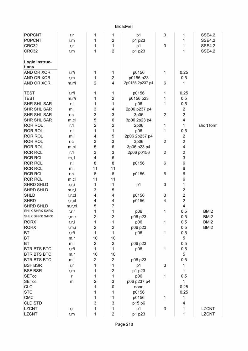
Broadwell
Page 218
POPCNT r,r 1 1 p1 3 1 SSE4.2POPCNT r,m 1 2 p1 p23 1 SSE4.2CRC32 r,r 1 1 p1 3 1 SSE4.2CRC32 r,m 1 2 p1 p23 1 SSE4.2
AND OR XOR r,r/i 1 1 p0156 1 0.25AND OR XOR r,m 1 2 p0156 p23 0.5AND OR XOR m,r/i 2 4 2p0156 2p237 p4 6 1
TEST r,r/i 1 1 p0156 1 0.25TEST m,r/i 1 2 p0156 p23 1 0.5SHR SHL SAR r,i 1 1 p06 1 0.5SHR SHL SAR m,i 3 4 2p06 p237 p4 2SHR SHL SAR r,cl 3 3 3p06 2 2SHR SHL SAR m,cl 5 6 3p06 2p23 p4 4ROR ROL r,1 2 2 2p06 1 1 short formROR ROL r,i 1 1 p06 1 0.5ROR ROL m,i 4 5 2p06 2p237 p4 2ROR ROL r,cl 3 3 3p06 2 2ROR ROL m,cl 5 6 3p06 p23 p4 4RCR RCL r,1 3 3 2p06 p0156 2 2RCR RCL m,1 4 6 3RCR RCL r,i 8 8 p0156 6 6RCR RCL m,i 11 11 6RCR RCL r,cl 8 8 p0156 6 6RCR RCL m,cl 11 11 6SHRD SHLD r,r,i 1 1 p1 3 1SHRD SHLD m,r,i 3 5 2SHLD r,r,cl 4 4 p0156 3 2SHRD r,r,cl 4 4 p0156 4 2SHRD SHLD m,r,cl 5 7 4SHLX SHRX SARX r,r,r 1 1 p06 1 0.5 BMI2SHLX SHRX SARX r,m,r 2 2 p06 p23 0.5 BMI2RORX r,r,i 1 1 p06 1 0.5 BMI2RORX r,m,i 2 2 p06 p23 0.5 BMI2BT r,r/i 1 1 p06 1 0.5BT m,r 10 10 5BT m,i 2 2 p06 p23 0.5BTR BTS BTC r,r/i 1 1 p06 1 0.5BTR BTS BTC m,r 10 10 5BTR BTS BTC m,i 2 2 p06 p23 0.5BSF BSR r,r 1 1 p1 3 1BSF BSR r,m 1 2 p1 p23 1SETcc r 1 1 p06 1 0.5SETcc m 2 3 p06 p237 p4 1CLC 1 0 none 0.25STC 1 1 p0156 0.25CMC 1 1 p0156 1 1CLD STD 3 3 p15 p6 4LZCNT r,r 1 1 p1 3 1 LZCNTLZCNT r,m 1 2 p1 p23 1 LZCNT
Logic instruc-tions

Broadwell
Page 219
TZCNT r,r 1 1 p1 3 1 BMI1TZCNT r,m 1 2 p1 p23 1 BMI1ANDN r,r,r 1 1 p15 1 0.5 BMI1ANDN r,r,m 1 2 p15 p23 1 0.5 BMI1
r,r 1 1 p15 1 0.5 BMI1
r,m 1 2 p15 p23 0.5 BMI1
BEXTR r,r,r 2 2 2p0156 2 0.5 BMI1BEXTR r,m,r 3 3 2p0156 p23 1 BMI1BZHI r,r,r 1 1 p15 1 0.5 BMI2BZHI r,m,r 1 2 p15 p23 0.5 BMI2PDEP r,r,r 1 1 p1 3 1 BMI2PDEP r,r,m 1 2 p1 p23 1 BMI2PEXT r,r,r 1 1 p1 3 1 BMI2PEXT r,r,m 1 2 p1 p23 1 BMI2
Control transfer instructionsJMP short/near 1 1 p6 1-2JMP r 1 1 p6 2JMP m 1 2 p23 p6 2Conditional jump short/near 1 1 p6 1-2
Conditional jump short/near 1 1 p06 0.5-1
1 1 p6 1-2
1 1 p06 0.5-1
J(E/R)CXZ short 2 2 p0156 p6 0.5-2LOOP short 7 7 5LOOP(N)E short 11 11 6CALL near 2 3 p237 p4 p6 2CALL r 2 3 p237 p4 p6 2CALL m 3 4 2p237 p4 p6 3RET 1 2 p237 p6 1RET i 3 4 p23 2p6 p015 2BOUND r,m 15 15 8 not 64 bitINTO 4 4 5 not 64 bit
LODSB/W 3 3 2p0156 p23 1LODSD/Q 2 2 p0156 p23 1REP LODS 5n+12 ~2nSTOS 3 3 p23 p0156 p4 1REP STOS <2n ~0.5n worst caseREP STOS 2.6/32B 1/32B
MOVS 5 5 2p23 p4 2p0156 4REP MOVS ~2n < 1n worst caseREP MOVS 4/32B 1/32B
BLSI BLSMSK BLSR
BLSI BLSMSK BLSR
predicted taken
predicted not taken
Fused arithmetic and branch
predicted taken
Fused arithmetic and branch
predicted not taken
String instruc-tions
best casealigned by 32
best casealigned by 32

Broadwell
Page 220
SCAS 3 3 p23 2p0156 1REP SCAS ≥6n ≥2nCMPS 5 5 2p23 3p0156 4REP CMPS ≥8n ≥2n
Synchronization instructionsXADD m,r 4 5 6LOCK XADD m,r 9 9 21LOCK ADD m,r 8 8 21CMPXCHG m,r 5 6 7LOCK CMPXCHG m,r 10 10 21CMPXCHG8B m,r 15 15 8LOCK CMPXCHG8B m,r 19 19 21CMPXCHG16B m,r 22 22 15LOCK CMPXCHG16B m,r 24 24 27
OtherNOP (90) 1 0 none 0.25
1 0 none 0.25
PAUSE 5 5 p05 3p6 9ENTER a,0 12 12 8ENTER a,b ~14+7b ~45+7b ~87+2bLEAVE 3 3 2p0156 p23 5XGETBV 8 8 5 XGETBVRDTSC 15 15 24RDTSCP 21 21 30 RDTSCPRDPMC 34 34 37RDRAND r 16 16 p23 15p0156 ~230 RDRANDRDSEED r 16 16 p23 15p0156 ~230 RDSEED
Floating point x87 instructions
Instruction Operands µops each port Latency Comments
FLD r 1 1 p01 1 0.5FLD m32/64 1 1 p23 3 0.5FLD m80 4 4 2p01 2p23 4 2FBLD m80 43 43 47 22FST(P) r 1 1 p01 1 0.5FST(P) m32/m64 1 2 p4 p237 4 1FSTP m80 7 7 3p0156 2p23 2p4 5 5FBSTP m80 238 226 269 267FXCH r 2 0 none 0 0.5FILD m 1 2 p01 p23 6 1FIST(P) m 3 3 p1 p23 p4 7 1FISTTP m 3 3 p1 p23 p4 7 2 SSE3FLDZ 1 1 p01 1FLD1 2 2 2p01 2
Long NOP (0F 1F)
µops fused domain
µops unfused domain
Recipro-cal throughput
Move instruc-tions
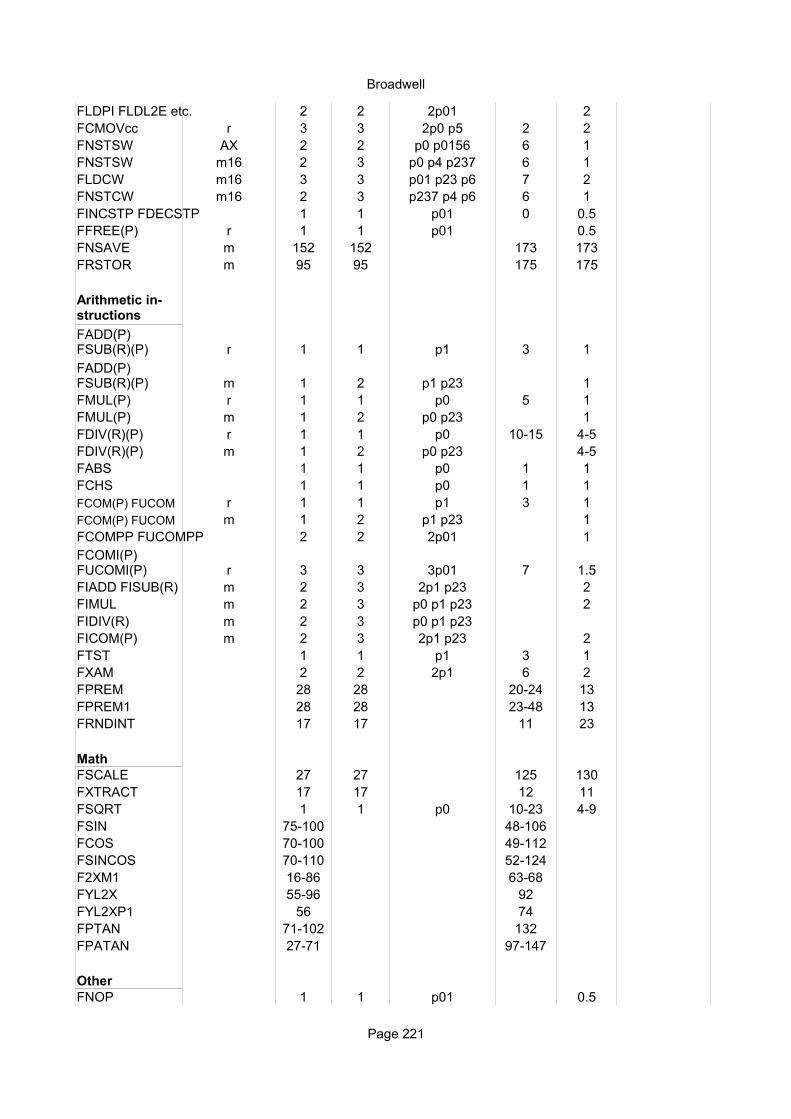
Broadwell
Page 221
FLDPI FLDL2E etc. 2 2 2p01 2FCMOVcc r 3 3 2p0 p5 2 2FNSTSW AX 2 2 p0 p0156 6 1FNSTSW m16 2 3 p0 p4 p237 6 1FLDCW m16 3 3 p01 p23 p6 7 2FNSTCW m16 2 3 p237 p4 p6 6 1FINCSTP FDECSTP 1 1 p01 0 0.5FFREE(P) r 1 1 p01 0.5FNSAVE m 152 152 173 173FRSTOR m 95 95 175 175
r 1 1 p1 3 1
m 1 2 p1 p23 1FMUL(P) r 1 1 p0 5 1FMUL(P) m 1 2 p0 p23 1FDIV(R)(P) r 1 1 p0 10-15 4-5FDIV(R)(P) m 1 2 p0 p23 4-5FABS 1 1 p0 1 1FCHS 1 1 p0 1 1FCOM(P) FUCOM r 1 1 p1 3 1FCOM(P) FUCOM m 1 2 p1 p23 1FCOMPP FUCOMPP 2 2 2p01 1
r 3 3 3p01 7 1.5FIADD FISUB(R) m 2 3 2p1 p23 2FIMUL m 2 3 p0 p1 p23 2FIDIV(R) m 2 3 p0 p1 p23FICOM(P) m 2 3 2p1 p23 2FTST 1 1 p1 3 1FXAM 2 2 2p1 6 2FPREM 28 28 20-24 13FPREM1 28 28 23-48 13FRNDINT 17 17 11 23
MathFSCALE 27 27 125 130FXTRACT 17 17 12 11FSQRT 1 1 p0 10-23 4-9FSIN 75-100 48-106FCOS 70-100 49-112FSINCOS 70-110 52-124F2XM1 16-86 63-68FYL2X 55-96 92FYL2XP1 56 74FPTAN 71-102 132FPATAN 27-71 97-147
OtherFNOP 1 1 p01 0.5
Arithmetic in-structions
FADD(P)FSUB(R)(P)
FADD(P)FSUB(R)(P)
FCOMI(P) FUCOMI(P)

Broadwell
Page 222
WAIT 2 2 p01 1FNCLEX 5 5 p0156 22FNINIT 26 26 84
Integer vector instructions
Instruction Operands µops each port Latency Comments
MOVD r32/64,(x)mm 1 1 p0 1 1MOVD m32/64,(x)mm 1 2 p237 p4 3 1MOVD (x)mm,r32/64 1 1 p5 1 1MOVD (x)mm,m32/64 1 1 p23 3 0.5MOVQ r64,(x)mm 1 1 p0 1 1MOVQ (x)mm,r64 1 1 p5 1 1MOVQ (x)mm,(x)mm 1 p015 1 0.33MOVQ (x)mm,m64 1 1 p23 3 0.5MOVQ m64, (x)mm 1 2 p237 p4 3 1MOVDQA/U x,x 1 1 p015 0-1 0.25 may be elim.MOVDQA/U x, m128 1 1 p23 3 0.5MOVDQA/U m128, x 1 2 p237 p4 3 1
VMOVDQA/U y,y 1 1 p015 0-1 0.25VMOVDQA/U y,m256 1 1 p23 3 0.5 AVXVMOVDQA/U m256,y 1 2 p237 p4 4 1 AVXLDDQU x, m128 1 1 p23 3 0.5 SSE3MOVDQ2Q mm, x 2 2 p01 p5 1 1MOVQ2DQ x,mm 1 1 p015 1 0.33MOVNTQ m64,mm 1 2 p237 p4 ~400 1MOVNTDQ m128,x 1 2 p237 p4 ~400 1VMOVNTDQ m256,y 1 2 p237 p4 ~400 1 AVX2MOVNTDQA x, m128 1 1 p23 3 0.5 SSE4.1VMOVNTDQA y,m256 1 1 p23 3 0.5 AVX2
mm,mm 3 3 p5 2 2
mm,m64 3 3 p23 2p5 2
x,x / y,y,y 1 1 p5 1 1
x,m / y,y,m 1 2 p23 p5 1PACKUSDW x,x / y,y,y 1 1 p5 1 1 SSE4.1PACKUSDW x,m / y,y,m 1 2 p23 p5 1 SSE4.1
v,v / v,v,v 1 1 p5 1 1
v,m / v,v,m 1 2 p23 p5 1
x,x / y,y,y 1 1 p5 1 1
x,m / y,y,m 2 2 p23 p5 1
µops fused domain
µops unfused domain
Recipro-cal throughput
Move instruc-tions
AVXmay be elim.
PACKSSWB/DW PACKUSWB
PACKSSWB/DW PACKUSWB
PACKSSWB/DW PACKUSWB
PACKSSWB/DW PACKUSWB
PUNPCKH/LBW/WD/DQ
PUNPCKH/LBW/WD/DQ
PUNPCKH/LQDQ
PUNPCKH/LQDQ
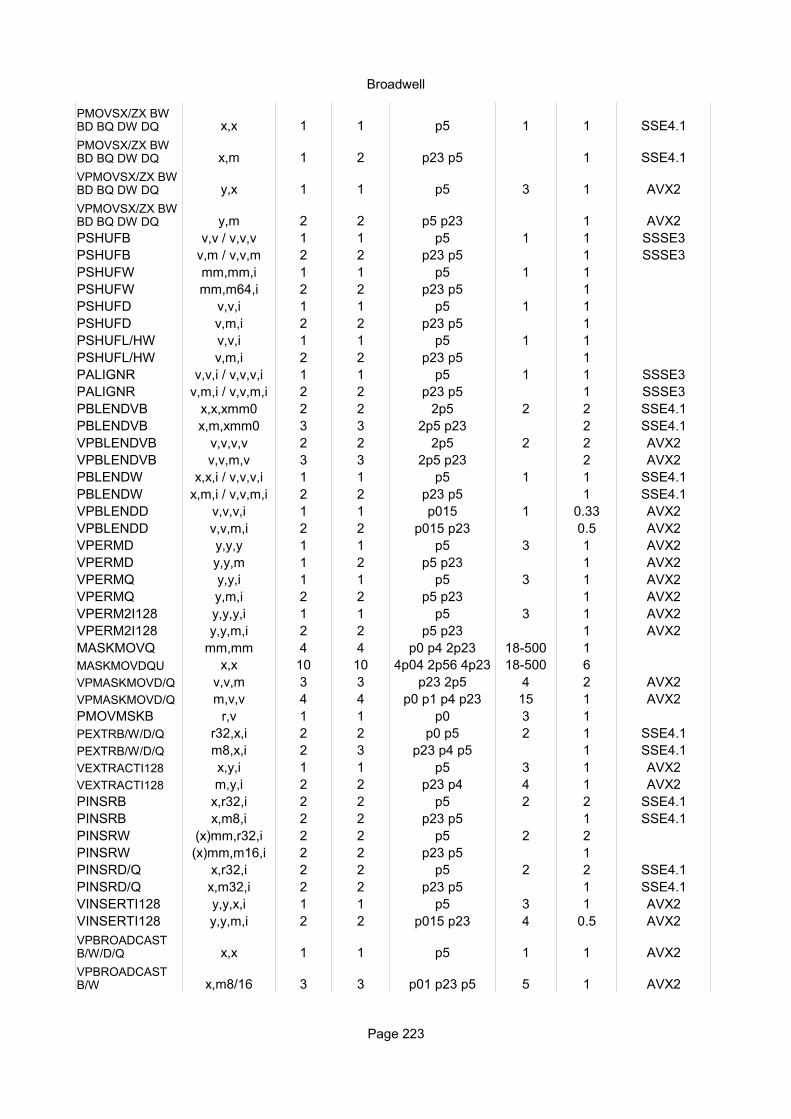
Broadwell
Page 223
x,x 1 1 p5 1 1 SSE4.1
x,m 1 2 p23 p5 1 SSE4.1
y,x 1 1 p5 3 1 AVX2
y,m 2 2 p5 p23 1 AVX2PSHUFB v,v / v,v,v 1 1 p5 1 1 SSSE3PSHUFB v,m / v,v,m 2 2 p23 p5 1 SSSE3PSHUFW mm,mm,i 1 1 p5 1 1PSHUFW mm,m64,i 2 2 p23 p5 1PSHUFD v,v,i 1 1 p5 1 1PSHUFD v,m,i 2 2 p23 p5 1PSHUFL/HW v,v,i 1 1 p5 1 1PSHUFL/HW v,m,i 2 2 p23 p5 1PALIGNR v,v,i / v,v,v,i 1 1 p5 1 1 SSSE3PALIGNR v,m,i / v,v,m,i 2 2 p23 p5 1 SSSE3PBLENDVB x,x,xmm0 2 2 2p5 2 2 SSE4.1PBLENDVB x,m,xmm0 3 3 2p5 p23 2 SSE4.1VPBLENDVB v,v,v,v 2 2 2p5 2 2 AVX2VPBLENDVB v,v,m,v 3 3 2p5 p23 2 AVX2PBLENDW x,x,i / v,v,v,i 1 1 p5 1 1 SSE4.1PBLENDW x,m,i / v,v,m,i 2 2 p23 p5 1 SSE4.1VPBLENDD v,v,v,i 1 1 p015 1 0.33 AVX2VPBLENDD v,v,m,i 2 2 p015 p23 0.5 AVX2VPERMD y,y,y 1 1 p5 3 1 AVX2VPERMD y,y,m 1 2 p5 p23 1 AVX2VPERMQ y,y,i 1 1 p5 3 1 AVX2VPERMQ y,m,i 2 2 p5 p23 1 AVX2VPERM2I128 y,y,y,i 1 1 p5 3 1 AVX2VPERM2I128 y,y,m,i 2 2 p5 p23 1 AVX2MASKMOVQ mm,mm 4 4 p0 p4 2p23 18-500 1MASKMOVDQU x,x 10 10 4p04 2p56 4p23 18-500 6VPMASKMOVD/Q v,v,m 3 3 p23 2p5 4 2 AVX2VPMASKMOVD/Q m,v,v 4 4 p0 p1 p4 p23 15 1 AVX2PMOVMSKB r,v 1 1 p0 3 1PEXTRB/W/D/Q r32,x,i 2 2 p0 p5 2 1 SSE4.1PEXTRB/W/D/Q m8,x,i 2 3 p23 p4 p5 1 SSE4.1VEXTRACTI128 x,y,i 1 1 p5 3 1 AVX2VEXTRACTI128 m,y,i 2 2 p23 p4 4 1 AVX2PINSRB x,r32,i 2 2 p5 2 2 SSE4.1PINSRB x,m8,i 2 2 p23 p5 1 SSE4.1PINSRW (x)mm,r32,i 2 2 p5 2 2PINSRW (x)mm,m16,i 2 2 p23 p5 1PINSRD/Q x,r32,i 2 2 p5 2 2 SSE4.1PINSRD/Q x,m32,i 2 2 p23 p5 1 SSE4.1VINSERTI128 y,y,x,i 1 1 p5 3 1 AVX2VINSERTI128 y,y,m,i 2 2 p015 p23 4 0.5 AVX2
x,x 1 1 p5 1 1 AVX2
x,m8/16 3 3 p01 p23 p5 5 1 AVX2
PMOVSX/ZX BW BD BQ DW DQ
PMOVSX/ZX BW BD BQ DW DQ
VPMOVSX/ZX BW BD BQ DW DQ
VPMOVSX/ZX BW BD BQ DW DQ
VPBROADCASTB/W/D/Q
VPBROADCASTB/W
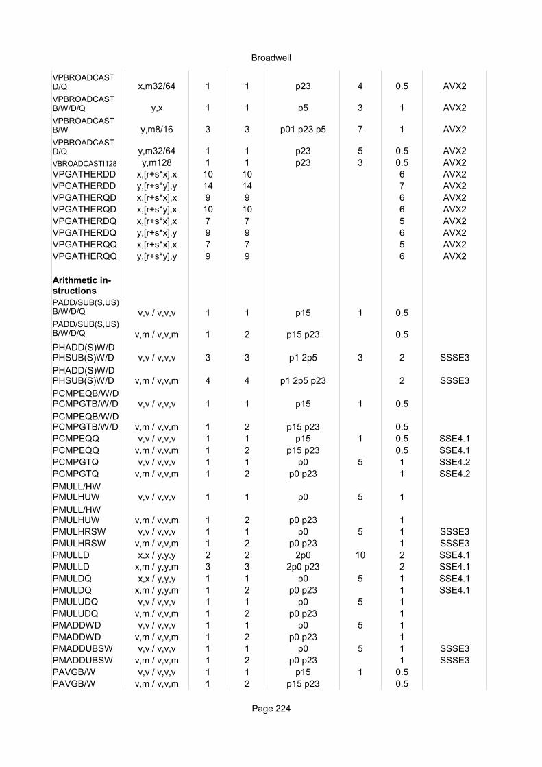
Broadwell
Page 224
x,m32/64 1 1 p23 4 0.5 AVX2
y,x 1 1 p5 3 1 AVX2
y,m8/16 3 3 p01 p23 p5 7 1 AVX2
y,m32/64 1 1 p23 5 0.5 AVX2VBROADCASTI128 y,m128 1 1 p23 3 0.5 AVX2VPGATHERDD x,[r+s*x],x 10 10 6 AVX2VPGATHERDD y,[r+s*y],y 14 14 7 AVX2VPGATHERQD x,[r+s*x],x 9 9 6 AVX2VPGATHERQD x,[r+s*y],x 10 10 6 AVX2VPGATHERDQ x,[r+s*x],x 7 7 5 AVX2VPGATHERDQ y,[r+s*x],y 9 9 6 AVX2VPGATHERQQ x,[r+s*x],x 7 7 5 AVX2VPGATHERQQ y,[r+s*y],y 9 9 6 AVX2
v,v / v,v,v 1 1 p15 1 0.5
v,m / v,v,m 1 2 p15 p23 0.5
v,v / v,v,v 3 3 p1 2p5 3 2 SSSE3
v,m / v,v,m 4 4 p1 2p5 p23 2 SSSE3
v,v / v,v,v 1 1 p15 1 0.5
v,m / v,v,m 1 2 p15 p23 0.5PCMPEQQ v,v / v,v,v 1 1 p15 1 0.5 SSE4.1PCMPEQQ v,m / v,v,m 1 2 p15 p23 0.5 SSE4.1PCMPGTQ v,v / v,v,v 1 1 p0 5 1 SSE4.2PCMPGTQ v,m / v,v,m 1 2 p0 p23 1 SSE4.2
v,v / v,v,v 1 1 p0 5 1
v,m / v,v,m 1 2 p0 p23 1PMULHRSW v,v / v,v,v 1 1 p0 5 1 SSSE3PMULHRSW v,m / v,v,m 1 2 p0 p23 1 SSSE3PMULLD x,x / y,y,y 2 2 2p0 10 2 SSE4.1PMULLD x,m / y,y,m 3 3 2p0 p23 2 SSE4.1PMULDQ x,x / y,y,y 1 1 p0 5 1 SSE4.1PMULDQ x,m / y,y,m 1 2 p0 p23 1 SSE4.1PMULUDQ v,v / v,v,v 1 1 p0 5 1PMULUDQ v,m / v,v,m 1 2 p0 p23 1PMADDWD v,v / v,v,v 1 1 p0 5 1PMADDWD v,m / v,v,m 1 2 p0 p23 1PMADDUBSW v,v / v,v,v 1 1 p0 5 1 SSSE3PMADDUBSW v,m / v,v,m 1 2 p0 p23 1 SSSE3PAVGB/W v,v / v,v,v 1 1 p15 1 0.5PAVGB/W v,m / v,v,m 1 2 p15 p23 0.5
VPBROADCASTD/Q
VPBROADCASTB/W/D/Q
VPBROADCASTB/W
VPBROADCASTD/Q
Arithmetic in-structionsPADD/SUB(S,US) B/W/D/Q
PADD/SUB(S,US) B/W/D/Q
PHADD(S)W/DPHSUB(S)W/D
PHADD(S)W/DPHSUB(S)W/D
PCMPEQB/W/DPCMPGTB/W/D
PCMPEQB/W/DPCMPGTB/W/D
PMULL/HWPMULHUW
PMULL/HWPMULHUW

Broadwell
Page 225
x,x / y,y,y 1 1 p15 1 0.5 SSE4.1
x,m / y,y,m 1 2 p15 p23 0.5 SSE4.1PHMINPOSUW x,x 1 1 p0 5 1 SSE4.1PHMINPOSUW x,m128 1 2 p0 p23 1 SSE4.1PABSB/W/D v,v 1 1 p15 1 0.5 SSSE3PABSB/W/D v,m 1 2 p15 p23 0.5 SSSE3PSIGNB/W/D v,v / v,v,v 1 1 p15 1 0.5 SSSE3PSIGNB/W/D v,m / v,v,m 1 2 p15 p23 0.5 SSSE3PSADBW v,v / v,v,v 1 1 p0 5 1PSADBW v,m / v,v,m 1 2 p0 p23 1MPSADBW x,x,i / v,v,v,i 3 3 p0 2p5 6 2 SSE4.1MPSADBW x,m,i / v,v,m,i 4 4 p0 2p5 p23 2 SSE4.1
v,v / v,v,v 1 1 p015 1 0.33
v,m / v,v,m 1 2 p015 p23 0.5PTEST v,v 2 2 p0 p5 2 1 SSE4.1PTEST v,m 2 3 p0 p5 p23 1 SSE4.1
mm,mm 1 1 p0 1 1
mm,m64 1 2 p0 p23 1
x,x / v,v,x 2 2 p0 p5 2 1
x,m / v,v,m 2 2 p0 p23 1
v,i / v,v,i 1 1 p0 1 1
v,v,v 3 3 2p0 p5 2 2 AVX2
v,v,m 4 4 2p0 p5 p23 2 AVX2
x,i / v,v,i 1 1 p5 1 1
PCMPESTRI x,x,i 8 8 6p05 2p16 4 4 SSE4.2PCMPESTRI x,m128,i 8 8 3p0 2p16 2p5 p23 4 SSE4.2PCMPESTRM x,x,i 9 9 3p0 2p16 4p5 11 11 SSE4.2
PMIN/PMAXSB/SW/SDUB/UW/UD
PMIN/PMAXSB/SW/SDUB/UW/UD
Logic instruc-tions
PAND PANDNPOR PXOR
PAND PANDNPOR PXOR
PSLLW/D/QPSRLW/D/QPSRAW/D/Q
PSLLW/D/QPSRLW/D/QPSRAW/D/Q
PSLLW/D/QPSRLW/D/QPSRAW/D/Q
PSLLW/D/QPSRLW/D/QPSRAW/D/Q
PSLLW/D/QPSRLW/D/QPSRAW/D/Q
VPSLLVD/QVPSRAVDVPSRLVD/Q
VPSLLVD/QVPSRAVDVPSRLVD/Q
PSLLDQPSRLDQ
String instruc-tions

Broadwell
Page 226
PCMPESTRM x,m128,i 9 9 6p05 2p16 p23 5 SSE4.2PCMPISTRI x,x,i 3 3 3p0 3 3 SSE4.2PCMPISTRI x,m128,i 4 4 3p0 p23 3 SSE4.2PCMPISTRM x,x,i 3 3 3p0 11 11 SSE4.2PCMPISTRM x,m128,i 4 4 3p0 p23 3 SSE4.2
Encryption instructionsPCLMULQDQ x,x,i 1 1 p0 5 1 CLMULPCLMULQDQ x,m,i 2 2 p0 p23 1 CLMUL
x,x 1 1 p5 7 1 AES
x,m 2 2 p5 p23 1.5 AESAESIMC x,x 2 2 2p5 14 2 AESAESIMC x,m 3 3 2p5 p23 2 AES
x,x,i 10 10 2p0 8p5 10 9 AES
x,m,i 10 10 2p0 p23 7p5 8 AES
OtherEMMS 31 31 12
Floating point XMM and YMM instructions
Instruction Operands µops each port Latency Comments
MOVAPS/D x,x 1 1 p5 0-1 1 may be elim.VMOVAPS/D y,y 1 1 p5 0-1 1 may be elim.
x,m128 1 1 p23 3 0.5
y,m256 1 1 p23 3 0.5 AVX
m128,x 1 2 p237 p4 3 1
m256,y 1 2 p237 p4 4 1 AVXMOVSS/D x,x 1 1 p5 1 1MOVSS/D x,m32/64 1 1 p23 3 0.5MOVSS/D m32/64,x 1 2 p237 p4 3 1MOVHPS/D x,m64 1 2 p23 p5 4 1MOVHPS/D m64,x 1 2 p4 p237 3 1MOVLPS/D x,m64 1 2 p23 p5 4 1MOVLPS/D m64,x 1 2 p4 p237 3 1MOVHLPS x,x 1 1 p5 1 1MOVLHPS x,x 1 1 p5 1 1
AESDEC, AESDECLAST, AESENC, AESENCLAST
AESDEC, AESDECLAST, AESENC, AESENCLAST
AESKEYGENASSIST
AESKEYGENASSIST
µops fused domain
µops unfused domain
Recipro-cal throughput
Move instruc-tions
MOVAPS/DMOVUPS/D
VMOVAPS/D VMOVUPS/D
MOVAPS/DMOVUPS/DVMOVAPS/D VMOVUPS/D
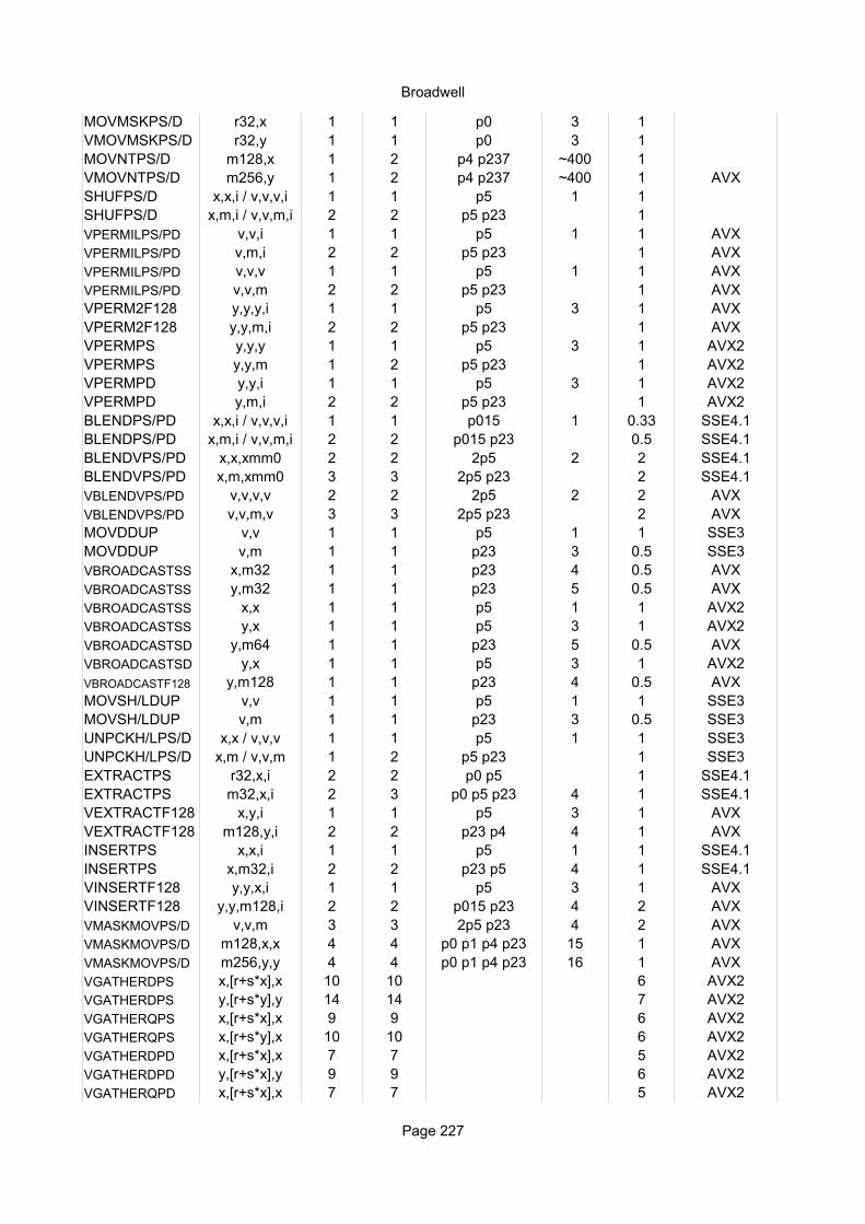
Broadwell
Page 227
MOVMSKPS/D r32,x 1 1 p0 3 1VMOVMSKPS/D r32,y 1 1 p0 3 1MOVNTPS/D m128,x 1 2 p4 p237 ~400 1VMOVNTPS/D m256,y 1 2 p4 p237 ~400 1 AVXSHUFPS/D x,x,i / v,v,v,i 1 1 p5 1 1SHUFPS/D x,m,i / v,v,m,i 2 2 p5 p23 1VPERMILPS/PD v,v,i 1 1 p5 1 1 AVXVPERMILPS/PD v,m,i 2 2 p5 p23 1 AVXVPERMILPS/PD v,v,v 1 1 p5 1 1 AVXVPERMILPS/PD v,v,m 2 2 p5 p23 1 AVXVPERM2F128 y,y,y,i 1 1 p5 3 1 AVXVPERM2F128 y,y,m,i 2 2 p5 p23 1 AVXVPERMPS y,y,y 1 1 p5 3 1 AVX2VPERMPS y,y,m 1 2 p5 p23 1 AVX2VPERMPD y,y,i 1 1 p5 3 1 AVX2VPERMPD y,m,i 2 2 p5 p23 1 AVX2BLENDPS/PD x,x,i / v,v,v,i 1 1 p015 1 0.33 SSE4.1BLENDPS/PD x,m,i / v,v,m,i 2 2 p015 p23 0.5 SSE4.1BLENDVPS/PD x,x,xmm0 2 2 2p5 2 2 SSE4.1BLENDVPS/PD x,m,xmm0 3 3 2p5 p23 2 SSE4.1VBLENDVPS/PD v,v,v,v 2 2 2p5 2 2 AVXVBLENDVPS/PD v,v,m,v 3 3 2p5 p23 2 AVXMOVDDUP v,v 1 1 p5 1 1 SSE3MOVDDUP v,m 1 1 p23 3 0.5 SSE3VBROADCASTSS x,m32 1 1 p23 4 0.5 AVXVBROADCASTSS y,m32 1 1 p23 5 0.5 AVXVBROADCASTSS x,x 1 1 p5 1 1 AVX2VBROADCASTSS y,x 1 1 p5 3 1 AVX2VBROADCASTSD y,m64 1 1 p23 5 0.5 AVXVBROADCASTSD y,x 1 1 p5 3 1 AVX2VBROADCASTF128 y,m128 1 1 p23 4 0.5 AVXMOVSH/LDUP v,v 1 1 p5 1 1 SSE3MOVSH/LDUP v,m 1 1 p23 3 0.5 SSE3UNPCKH/LPS/D x,x / v,v,v 1 1 p5 1 1 SSE3UNPCKH/LPS/D x,m / v,v,m 1 2 p5 p23 1 SSE3EXTRACTPS r32,x,i 2 2 p0 p5 1 SSE4.1EXTRACTPS m32,x,i 2 3 p0 p5 p23 4 1 SSE4.1VEXTRACTF128 x,y,i 1 1 p5 3 1 AVXVEXTRACTF128 m128,y,i 2 2 p23 p4 4 1 AVXINSERTPS x,x,i 1 1 p5 1 1 SSE4.1INSERTPS x,m32,i 2 2 p23 p5 4 1 SSE4.1VINSERTF128 y,y,x,i 1 1 p5 3 1 AVXVINSERTF128 y,y,m128,i 2 2 p015 p23 4 2 AVXVMASKMOVPS/D v,v,m 3 3 2p5 p23 4 2 AVXVMASKMOVPS/D m128,x,x 4 4 p0 p1 p4 p23 15 1 AVXVMASKMOVPS/D m256,y,y 4 4 p0 p1 p4 p23 16 1 AVXVGATHERDPS x,[r+s*x],x 10 10 6 AVX2VGATHERDPS y,[r+s*y],y 14 14 7 AVX2VGATHERQPS x,[r+s*x],x 9 9 6 AVX2VGATHERQPS x,[r+s*y],x 10 10 6 AVX2VGATHERDPD x,[r+s*x],x 7 7 5 AVX2VGATHERDPD y,[r+s*x],y 9 9 6 AVX2VGATHERQPD x,[r+s*x],x 7 7 5 AVX2

Broadwell
Page 228
VGATHERQPD y,[r+s*y],y 9 9 6 AVX2
ConversionCVTPD2PS x,x 2 2 p1 p5 4 1CVTPD2PS x,m128 2 3 p1 p5 p23 1VCVTPD2PS x,y 2 2 p1 p5 5 1 AVXVCVTPD2PS x,m256 2 3 p1 p5 p23 1 AVXCVTSD2SS x,x 2 2 p1 p5 4 1CVTSD2SS x,m64 2 3 p1 p5 p23 1CVTPS2PD x,x 2 2 p0 p5 2 1CVTPS2PD x,m64 2 2 p0 p23 1VCVTPS2PD y,x 2 2 p0 p5 5 1 AVXVCVTPS2PD y,m128 2 2 p0 p23 1 AVXCVTSS2SD x,x 2 2 p0 p5 2 1CVTSS2SD x,m32 2 2 p0 p23 1CVTDQ2PS x,x 1 1 p1 3 1CVTDQ2PS x,m128 1 2 p1 p23 1VCVTDQ2PS y,y 1 1 p1 3 1 AVXVCVTDQ2PS y,m256 1 2 p1 p23 1 AVXCVT(T) PS2DQ x,x 1 1 p1 3 1CVT(T) PS2DQ x,m128 1 2 p1 p23 1VCVT(T) PS2DQ y,y 1 1 p1 3 1 AVXVCVT(T) PS2DQ y,m256 1 2 p1 p23 1 AVXCVTDQ2PD x,x 2 2 p1 p5 4 1CVTDQ2PD x,m64 2 2 p1 p23 1VCVTDQ2PD y,x 2 2 p1 p5 6 1 AVXVCVTDQ2PD y,m128 2 2 p1 p23 1 AVXCVT(T)PD2DQ x,x 2 2 p1 p5 4 1CVT(T)PD2DQ x,m128 2 3 p1 p5 p23 1VCVT(T)PD2DQ x,y 2 2 p1 p5 6 1 AVXVCVT(T)PD2DQ x,m256 2 3 p1 p5 p23 1 AVXCVTPI2PS x,mm 1 1 p1 4 4CVTPI2PS x,m64 1 2 p1 p23 3CVT(T)PS2PI mm,x 2 2 p1 p5 4 1CVT(T)PS2PI mm,m128 2 2 p1 p23 1CVTPI2PD x,mm 2 2 p1 p5 4 1CVTPI2PD x,m64 2 2 p1 p23 1CVT(T) PD2PI mm,x 2 2 p1 p5 4 1CVT(T) PD2PI mm,m128 2 3 p1 p5 p23 1CVTSI2SS x,r32 2 2 p1 p5 4 3CVTSI2SS x,r64 3 3 p1 2p5 5 4CVTSI2SS x,m32 1 2 p1 p23 3CVT(T)SS2SI r32,x 2 2 p0 p1 4 1CVT(T)SS2SI r32,m32 2 3 p0 p1 p23 1CVTSI2SD x,r32/64 2 2 p1 p5 4 3CVTSI2SD x,m32 2 2 p1 p23 3CVT(T)SD2SI r32/64,x 2 2 p0 p1 4 1CVT(T)SD2SI r32,m64 2 3 p0 p1 p23 1VCVTPS2PH x,v,i 2 2 p1 p5 4-6 1 F16CVCVTPS2PH m,v,i 3 3 p1 p4 p23 1 F16CVCVTPH2PS v,x 2 2 p1 p5 4-6 1 F16CVCVTPH2PS v,m 2 2 p1 p23 1 F16C

Broadwell
Page 229
Arithmetic
x,x / v,v,v 1 1 p1 3 1
x,m / v,v,m 1 2 p1 p23 1ADDSUBPS/D x,x / v,v,v 1 1 p1 3 1 SSE3ADDSUBPS/D x,m / v,v,m 1 2 p1 p23 1 SSE3
x,x / v,v,v 3 3 p1 2p5 5 2 SSE3
x,m / v,v,m 4 4 p1 2p5 p23 2 SSE3MULSS/D PS/D x,x / v,v,v 1 1 p01 3 0.5MULSS/D PS/D x,m / v,v,m 1 2 p01 p23 0.5DIVSS x,x 1 1 p0 11 2.5DIVPS x,x 1 1 p0 11 5DIVSS DIVPS x,m 1 2 p0 p23 3-5DIVSD x,x 1 1 p0 10-14 4-5DIVPD x,x 1 1 p0 10-14 8DIVSD DIVPD x,m 1 2 p0 p23 4-5VDIVPS y,y,y 3 3 2p0 p15 17 10 AVXVDIVPS y,y,m256 4 4 2p0 p15 p23 10 AVXVDIVPD y,y,y 3 3 2p0 p15 19-23 16 AVXVDIVPD y,y,m256 4 4 2p0 p15 p23 16 AVXRCPSS/PS x,x 1 1 p0 5 1RCPSS/PS x,m128 1 2 p0 p23 1VRCPPS y,y 3 3 2p0 p15 7 2 AVXVRCPPS y,m256 4 4 2p0 p15 p23 2 AVX
x,x / v,v,v 1 1 p1 3 1
x,m / v,v,m 2 2 p1 p23 1(U)COMISS/D x,x 1 1 p1 1(U)COMISS/D x,m32/64 2 2 p1 p23 1
x,x / v,v,v 1 1 p1 3 1
x,m / v,v,m 1 2 p1 p23 1
ROUNDSS/D PS/D v,v,i 2 2 2p1 6 2 SSE4.1
ROUNDSS/D PS/D v,m,i 3 3 2p1 p23 2 SSE4.1DPPS x,x,i / v,v,v,i 4 4 2p0 p1 p5 12 2 SSE4.1DPPS x,m,i / v,v,m,i 6 6 2p0 p1 p5 p23 p6 4 SSE4.1DPPD x,x,i 3 3 p0 p1 p5 7 1 SSE4.1DPPD x,m128,i 4 4 p0 p1 p5 p23 1 SSE4.1
v,v,v 1 1 p01 5 0.5 FMA
v,v,m 1 2 p01 p23 0.5 FMA
MathSQRTSS x,x 1 1 p0 11 4
ADDSS/D PS/DSUBSS/D PS/D
ADDSS/D PS/DSUBSS/D PS/D
HADDPS/DHSUBPS/D
HADDPS/DHSUBPS/D
CMPccSS/D CMPccPS/D
CMPccSS/D CMPccPS/D
MAXSS/D PS/DMINSS/D PS/D
MAXSS/D PS/DMINSS/D PS/D
VFMADD...(all FMA instr.)
VFMADD...(all FMA instr.)

Broadwell
Page 230
SQRTPS x,x 1 1 p0 11 7SQRTSS/PS x,m128 1 2 p0 p23 4-7VSQRTPS y,y 3 3 2p0 p15 19 14 AVXVSQRTPS y,m256 4 4 2p0 p15 p23 14 AVXSQRTSD x,x 1 1 p0 15-16 4-8SQRTPD x,x 1 1 p0 15-16 8-14SQRTSD/PD x,m128 1 2 p0 p23 4-14VSQRTPD y,y 3 3 2p0 p15 27-29 16-28 AVXVSQRTPD y,m256 4 4 2p0 p15 p23 16-28 AVXRSQRTSS/PS x,x 1 1 p0 5 1RSQRTSS/PS x,m128 1 2 p0 p23 1VRSQRTPS y,y 3 3 2p0 p15 7 2 AVXVRSQRTPS y,m256 4 4 2p0 p15 p23 2 AVX
Logic
x,x / v,v,v 1 1 p5 1 1
x,m / v,v,m 1 2 p5 p23 1
OtherVZEROUPPER 4 4 none 1 AVX
VZEROALL 12 12 none 10
VZEROALL 20 20 none 8LDMXCSR m32 3 3 p0 p6 p23 6 3STMXCSR m32 3 4 p0 p4 p6 p237 7 1FXSAVE m4096 111 66 66 32 bit modeFXSAVE m4096 141 66 66 64 bit modeFXRSTOR m4096 107 80 80 32 bit modeFXRSTOR m4096 115 80 80 64 bit modeXSAVE 174 70 70 32 bit modeXSAVE 224 84 84 64 bit modeXRSTOR 172 111 111 32 bit modeXRSTOR 173 112 112 64 bit modeXSAVEOPT m 114 51 51
AND/ANDN/OR/XORPS/PD
AND/ANDN/OR/XORPS/PD
AVX,32 bit
AVX,64 bit

Skylake
Page 231
Intel SkylakeList of instruction timings and μop breakdown
Explanation of column headings:Instruction:
Operands:
µops each port:
Latency:
Integer instructions
Instruction Operands µops each port Latency Comments
MOV r,i 1 1 p0156 0.25MOV r8/16,r8/16 1 1 p0156 1 0.25MOV r32/64,r32/64 1 1 p0156 0-1 0.25 may be elim.MOV r8l,m 1 2 p23 p0156 0.5MOV r8h,m 1 1 p23 0.5MOV r16,m 1 2 p23 p0156 0.5MOV r32/64,m 1 1 p23 2 0.5
Name of instruction. Multiple names mean that these instructions have the same data. Instructions with or without V name prefix behave the same unless otherwise noted.
i = immediate data, r = register, mm = 64 bit mmx register, x = 128 bit xmm register, (x)mm = mmx or xmm register, y = 256 bit ymm register, v = any vector register (mmx, xmm, ymm). same = same register for both operands. m = memory operand, m32 = 32-bit memory operand, etc.
μops fused domain:
The number of μops at the decode, rename and allocate stages in the pipeline. Fused μops count as one.
μops unfused domain:
The total number of μops for all execution port. Fused μops count as two. Fused macro-ops count as one. The instruction has μop fusion if this number is higher than the num-ber under fused domain. Some operations are not counted here if they do not go to any execution port or if the counters are inaccurate.
The number of μops for each execution port. p0 means a µop to execution port 0. p01means a µop that can go to either port 0 or port 1. p0 p1 means two µops going to port 0 and 1, respectively.Port 0: Integer, f.p. and vector ALU, mul, div, branchPort 1: Integer, f.p. and vector ALUPort 2: LoadPort 3: LoadPort 4: StorePort 5: Integer and vector ALUPort 6: Integer ALU, branchPort 7: Store address
This is the delay that the instruction generates in a dependency chain. The numbers are minimum values. Cache misses, misalignment, and exceptions may increase the clock counts considerably. Where hyperthreading is enabled, the use of the same execution units in the other thread leads to inferior performance. Denormal numbers, NAN's and in-finity do not increase the latency. The time unit used is core clock cycles, not the refer-ence clock cycles given by the time stamp counter.
Reciprocal throughput:
The average number of core clock cycles per instruction for a series of independent in-structions of the same kind in the same thread.
µops fused domain
µops unfused domain
Recipro-cal throughput
Move instruc-tions
all addressing modes

Skylake
Page 232
MOV m,r 1 2 p237 p4 2 1MOV m,i 1 2 p237 p4 1MOVNTI m,r 2 2 p23 p4 ~400 1
r,r 1 1 p0156 1 0.25
MOVSX MOVZX r16,m8 1 2 p23 p0156 0.5r,m 1 1 p23 0.5
CMOVcc r,r 1 1 p06 1 0.5CMOVcc r,m 2 2 p06 p23 0.5XCHG r,r 3 3 3p0156 2 1XCHG r,m 8 8 23 implicit lockXLAT 3 3 p23 2p0156 7 2PUSH r 1 2 p237 p4 3 1PUSH i 1 2 p237 p4 1PUSH m 2 3 p4 2p237 1PUSH stack pointer 2 3 p0156 p237 p4 1PUSHF(D/Q) 3 4 p1 p4 p237 p06 1PUSHA(D) 11 19 8 not 64 bitPOP r 1 1 p23 2 0.5POP stack pointer 3 3 p23 2p0156 3POP m 2 3 2p237 p4 1POPF(D/Q) 9 9 20POPA(D) 18 18 8 not 64 bitLAHF SAHF 1 1 p06 1 1SALC 3 3 3p0156 1 1 not 64 bitLEA r16,m 2 2 p1 p05 2-4 1
LEA r32/64,m 1 1 p15 1 0.5
LEA r32/64,m 1 1 p1 3 1
LEA r32/64,m 1 1 p1 1
BSWAP r32 1 1 p15 1 0.5BSWAP r64 2 2 p06 p15 2 1MOVBE r16,m16 3 3 2p0156 p23 0.5-1 MOVBEMOVBE r32,m32 2 2 p15 p23 0.5 MOVBEMOVBE r64,m64 3 3 2p0156 p23 0.75 MOVBEMOVBE m16,r16 2 3 p06 p237 p4 1 MOVBEMOVBE m32,r32 2 3 p15 p237 p4 1 MOVBEMOVBE m64,r64 3 4 p06 p15 p237 p4 1 MOVBE
m 1 1 p23 0.5
PREFETCHW m 1 1 p23 1 PREFETCHW
LFENCE 2 none counted 4MFENCE 4 4 p23 p4 33SFENCE 2 2 p23 p4 6
MOVSX MOVZX MOVSXD
MOVSX MOVZX MOVSXD
all othercombinations
16 or 32 bit address size
1 or 2 compo-nents inaddress
3 components in address
rip relativeaddress
PREFETCHNTA/0/1/2
Arithmetic in-structions

Skylake
Page 233
ADD SUB r,r/i 1 1 p0156 1 0.25ADD SUB r,m 1 2 p0156 p23 0.5ADD SUB m,r/i 2 4 2p0156 2p237 p4 5 1
ADC SBB r,r/i 1 1 p06 1 1ADC SBB r,m 2 2 p06 p23 1ADC SBB m,r/i 4 6 3p0156 2p237 p4 5 2
CMP r,r/i 1 1 p0156 1 0.25CMP m,r/i 1 2 p0156 p23 1 0.5
r 1 1 p0156 1 0.25
INC DEC NOT m 3 4 p0156 2p237 p4 5-6 1NEG m 2 4 p0156 2p237 p4 5-6 1AAA 2 2 p1 p56 4 not 64 bitAAS 2 2 p1 p056 4 not 64 bitDAA DAS 3 3 p1 2p056 4 not 64 bitAAD 3 3 p1 2p056 4 not 64 bitAAM 11 11 p0 p1 p5 p6 23 7 not 64 bitMUL IMUL r8 1 1 p1 3 1MUL IMUL r16 4 4 p1 p0156 4 2MUL IMUL r32 3 3 p1 p0156 4 1MUL IMUL r64 2 2 p1 p6 3 1MUL IMUL m8 1 2 p1 p23 1MUL IMUL m16 4 5 p1 3p0156 p23 2MUL IMUL m32 3 4 p1 2p0156 p23 2MUL IMUL m64 2 3 p1 p6 p23 1IMUL r,r 1 1 p1 3 1IMUL r,m 1 2 p1 p23 1IMUL r16,r16,i 2 2 p1 p0156 4 1IMUL r32,r32,i 1 1 p1 3 1IMUL r64,r64,i 1 1 p1 3 1IMUL r16,m16,i 2 3 p1 p0156 p23 1IMUL r32,m32,i 1 2 p1 p23 1IMUL r64,m64,i 1 2 p1 p23 1MULX r32,r32,r32 3 3 p1 2p056 4 1 BMI2MULX r32,r32,m32 3 4 p1 2p056 p23 1 BMI2MULX r64,r64,r64 2 2 p1 p5 4 1 BMI2MULX r64,r64,m64 2 3 p1 p6 p23 1 BMI2DIV r8 10 10 p0 p1 p5 p6 23 6DIV r16 10 10 p0 p1 p5 p6 23 6DIV r32 10 10 p0 p1 p5 p6 26 6DIV r64 36 36 p0 p1 p5 p6 35-88 21-83IDIV r8 11 11 p0 p1 p5 p6 24 6IDIV r16 10 10 p0 p1 p5 p6 23 6IDIV r32 10 10 p0 p1 p5 p6 26 6IDIV r64 57 57 p0 p1 p5 p6 42-95 24-90CBW 1 1 p0156 1CWDE 1 1 p0156 1CDQE 1 1 p0156 1CWD 2 2 p0156 1CDQ 1 1 p06 1
INC DEC NEG NOT

Skylake
Page 234
CQO 1 1 p06 1POPCNT r,r 1 1 p1 3 1 SSE4.2POPCNT r,m 1 2 p1 p23 1 SSE4.2CRC32 r,r 1 1 p1 3 1 SSE4.2CRC32 r,m 1 2 p1 p23 1 SSE4.2
AND OR XOR r,r/i 1 1 p0156 1 0.25AND OR XOR r,m 1 2 p0156 p23 0.5AND OR XOR m,r/i 2 4 2p0156 2p237 p4 5 1
TEST r,r/i 1 1 p0156 1 0.25TEST m,r/i 1 2 p0156 p23 1 0.5SHR SHL SAR r,i 1 1 p06 1 0.5SHR SHL SAR m,i 3 4 2p06 p237 p4 2SHR SHL SAR r,cl 3 3 3p06 2 2SHR SHL SAR m,cl 5 6 3p06 2p23 p4 4ROR ROL r,1 2 2 2p06 1 1 short formROR ROL r,i 1 1 p06 1 0.5ROR ROL m,i 4 5 2p06 2p237 p4 2ROR ROL r,cl 3 3 3p06 2 2ROR ROL m,cl 5 6 3p06 p23 p4 4RCR RCL r,1 3 3 2p06 p0156 2 2RCR RCL m,1 4 6 3RCR RCL r,i 8 8 p0156 6 6RCR RCL m,i 11 11 6RCR RCL r,cl 8 8 p0156 6 6RCR RCL m,cl 11 11 6SHRD SHLD r,r,i 1 1 p1 3 1SHRD SHLD m,r,i 3 5 2SHLD r,r,cl 4 4 p0156 3 2SHRD r,r,cl 4 4 p0156 4 2SHRD SHLD m,r,cl 5 7 4SHLX SHRX SARX r,r,r 1 1 p06 1 0.5 BMI2SHLX SHRX SARX r,m,r 2 2 p06 p23 0.5 BMI2RORX r,r,i 1 1 p06 1 0.5 BMI2RORX r,m,i 2 2 p06 p23 0.5 BMI2BT r,r/i 1 1 p06 1 0.5BT m,r 10 10 5BT m,i 2 2 p06 p23 0.5BTR BTS BTC r,r/i 1 1 p06 1 0.5BTR BTS BTC m,r 10 11 5BTR BTS BTC m,i 3 4 p06 p4 p23 1BSF BSR r,r 1 1 p1 3 1BSF BSR r,m 1 2 p1 p23 1SETcc r 1 1 p06 1 0.5SETcc m 2 3 p06 p237 p4 1CLC 1 0 none 0.25STC 1 1 p0156 0.25CMC 1 1 p0156 1 1CLD STD 3 3 p15 p6 4LZCNT r,r 1 1 p1 3 1 LZCNT
Logic instruc-tions

Skylake
Page 235
LZCNT r,m 1 2 p1 p23 1 LZCNTTZCNT r,r 1 1 p1 3 1 BMI1TZCNT r,m 1 2 p1 p23 1 BMI1ANDN r,r,r 1 1 p15 1 0.5 BMI1ANDN r,r,m 1 2 p15 p23 1 0.5 BMI1
r,r 1 1 p15 1 0.5 BMI1
r,m 1 2 p15 p23 0.5 BMI1
BEXTR r,r,r 2 2 2p0156 2 0.5 BMI1BEXTR r,m,r 3 3 2p0156 p23 1 BMI1BZHI r,r,r 1 1 p15 1 0.5 BMI2BZHI r,m,r 1 2 p15 p23 0.5 BMI2PDEP r,r,r 1 1 p1 3 1 BMI2PDEP r,r,m 1 2 p1 p23 1 BMI2PEXT r,r,r 1 1 p1 3 1 BMI2PEXT r,r,m 1 2 p1 p23 1 BMI2
Control transfer instructionsJMP short/near 1 1 p6 1-2JMP r 1 1 p6 2JMP m 1 2 p23 p6 2Conditional jump short/near 1 1 p6 1-2
Conditional jump short/near 1 1 p06 0.5-1
1 1 p6 1-2
1 1 p06 0.5-1
J(E/R)CXZ short 2 2 p0156 p6 0.5-2LOOP short 7 7 5LOOP(N)E short 11 11 6CALL near 2 3 p237 p4 p6 3CALL r 2 3 p237 p4 p6 2CALL m 3 4 2p237 p4 p6 3RET 1 2 p237 p6 1RET i 2 2BOUND r,m 15 15 8 not 64 bitINTO 5 5 6 not 64 bit
LODSB/W 3 3 2p0156 p23 1LODSD/Q 2 2 p0156 p23 1REP LODS 5n+12 ~2nSTOS 3 3 p23 p0156 p4 1REP STOS <2n ~0.5n worst caseREP STOS 2.6/32B 1/32B
MOVS 5 5 2p23 p4 2p0156 4REP MOVS ~2n < 1n worst case
BLSI BLSMSK BLSR
BLSI BLSMSK BLSR
predicted taken
predicted not taken
Fused arithmetic and branch
predicted taken
Fused arithmetic and branch
predicted not taken
String instruc-tions
best casealigned by 32
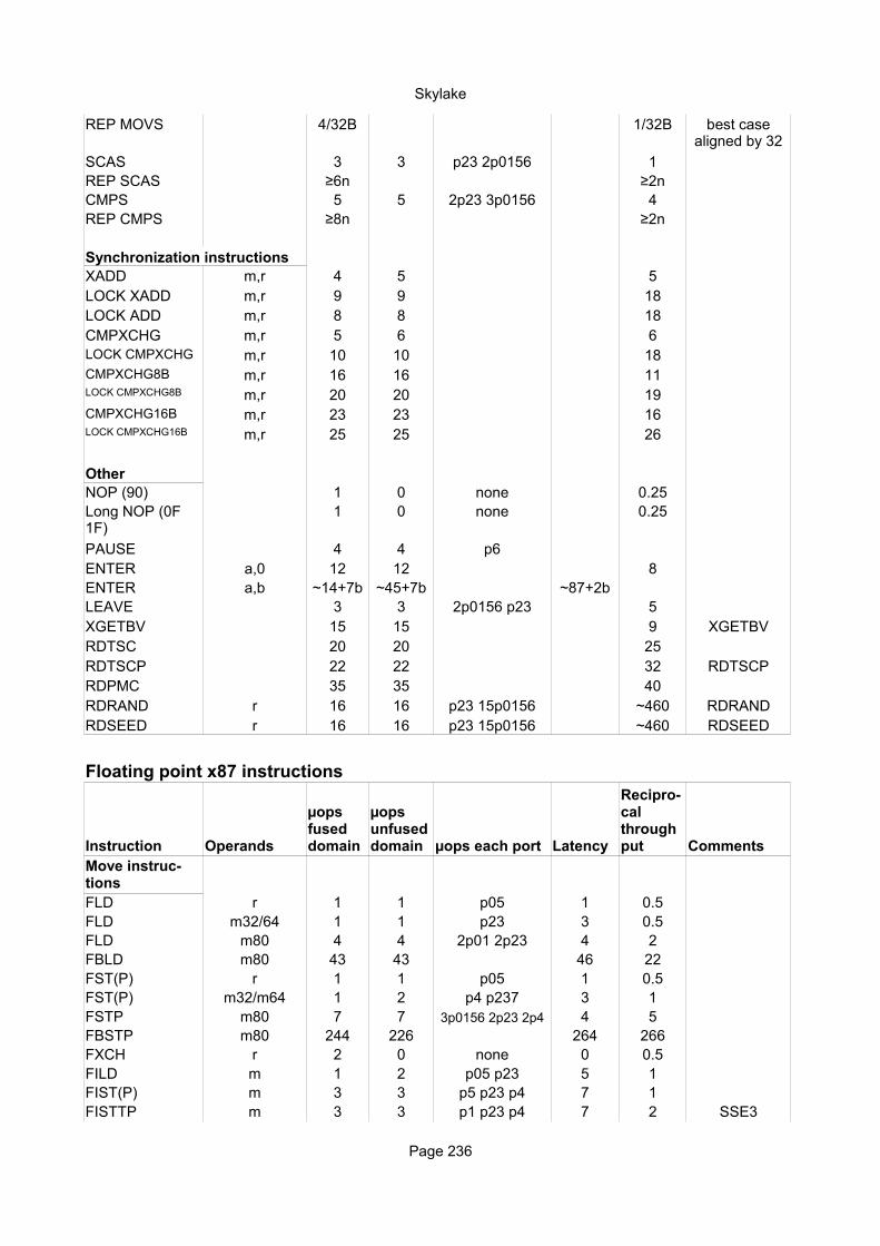
Skylake
Page 236
REP MOVS 4/32B 1/32B
SCAS 3 3 p23 2p0156 1REP SCAS ≥6n ≥2nCMPS 5 5 2p23 3p0156 4REP CMPS ≥8n ≥2n
Synchronization instructionsXADD m,r 4 5 5LOCK XADD m,r 9 9 18LOCK ADD m,r 8 8 18CMPXCHG m,r 5 6 6LOCK CMPXCHG m,r 10 10 18CMPXCHG8B m,r 16 16 11LOCK CMPXCHG8B m,r 20 20 19CMPXCHG16B m,r 23 23 16LOCK CMPXCHG16B m,r 25 25 26
OtherNOP (90) 1 0 none 0.25
1 0 none 0.25
PAUSE 4 4 p6ENTER a,0 12 12 8ENTER a,b ~14+7b ~45+7b ~87+2bLEAVE 3 3 2p0156 p23 5XGETBV 15 15 9 XGETBVRDTSC 20 20 25RDTSCP 22 22 32 RDTSCPRDPMC 35 35 40RDRAND r 16 16 p23 15p0156 ~460 RDRANDRDSEED r 16 16 p23 15p0156 ~460 RDSEED
Floating point x87 instructions
Instruction Operands µops each port Latency Comments
FLD r 1 1 p05 1 0.5FLD m32/64 1 1 p23 3 0.5FLD m80 4 4 2p01 2p23 4 2FBLD m80 43 43 46 22FST(P) r 1 1 p05 1 0.5FST(P) m32/m64 1 2 p4 p237 3 1FSTP m80 7 7 3p0156 2p23 2p4 4 5FBSTP m80 244 226 264 266FXCH r 2 0 none 0 0.5FILD m 1 2 p05 p23 5 1FIST(P) m 3 3 p5 p23 p4 7 1FISTTP m 3 3 p1 p23 p4 7 2 SSE3
best casealigned by 32
Long NOP (0F 1F)
µops fused domain
µops unfused domain
Recipro-cal throughput
Move instruc-tions

Skylake
Page 237
FLDZ 1 1 p05 1FLD1 2 2 2p05 2FLDPI FLDL2E etc. 2 2 2p05 2FCMOVcc r 4 4 p0 p1 p56 3 2FNSTSW AX 2 2 p0 p0156 6 2FNSTSW m16 2 3 p0 p4 p237 6 1FLDCW m16 3 3 p01 p23 p6 7 2FNSTCW m16 2 3 p237 p4 p6 6 1FINCSTP FDECSTP 1 1 p05 0 0.5FFREE(P) r 1 1 p05 0.5FNSAVE m 133 133 176 176FRSTOR m 89 89 175 175
r 1 1 p5 3 1
m 2 3 p5 p23 1FMUL(P) r 1 1 p0 5 1FMUL(P) m 2 3 p0 p23 1FDIV(R)(P) r 1 1 p0 14-16 4-5FDIV(R)(P) m 1 2 p0 p23 4-5FABS 1 1 p0 1 1FCHS 1 1 p0 1 1FCOM(P) FUCOM r 1 1 p5 3 1FCOM(P) FUCOM m 1 2 p5 p23 1FCOMPP FUCOMPP 2 2 p0 p5 1
r 3 3 p5 1FIADD FISUB(R) m 3 4 2p5 p23 2FIMUL m 2 3 p0 p5 p23 1FIDIV(R) m 2 3 p0 p5 p23FICOM(P) m 2 3 2p5 p23 2FTST 1 1 p5 3 1FXAM 2 2 2p5 6 2FPREM 31 31 26-30 17FPREM1 31 31 30-57 17FRNDINT 17 17 21 11
MathFSCALE 27 27 130 130FXTRACT 17 17 11 11FSQRT 1 1 p0 14-21 4-7FSIN 53-105 50-120FCOS 53-105 50-130FSINCOS 55-120 55-150F2XM1 16-90 65-80FYL2X 40-100 103FYL2XP1 56 77FPTAN 40-112 140-160FPATAN 30-160 100-160
Arithmetic in-structions
FADD(P)FSUB(R)(P)
FADD(P)FSUB(R)(P)
FCOMI(P) FUCOMI(P)

Skylake
Page 238
OtherFNOP 1 1 p05 0.5WAIT 2 2 p05 2FNCLEX 5 5 p156 22FNINIT 18 18 78
Integer vector instructions
Instruction Operands µops each port Latency Comments
MOVD r32/64,(x)mm 1 1 p0 2 1MOVD m32/64,(x)mm 1 2 p237 p4 3 1MOVD (x)mm,r32/64 1 1 p5 2 1MOVD (x)mm,m32/64 1 1 p23 2 0.5MOVQ r64,(x)mm 1 1 p0 2 1MOVQ (x)mm,r64 1 1 p5 1 1MOVQ mm,mm 1 p05 1 0.5MOVQ x,x 1 p015 1 0.33MOVQ (x)mm,m64 1 1 p23 2 0.5MOVQ m64, (x)mm 1 2 p237 p4 3 1MOVDQA/U x,x 1 1 p015 0-1 0.25 may eliminateMOVDQA/U x, m128 1 1 p23 2 0.5MOVDQA/U m128, x 1 2 p237 p4 3 1VMOVDQA/U y,y 1 1 p015 0-1 0.25 may eliminateVMOVDQA/U y,m256 1 1 p23 3 0.5 AVXVMOVDQA/U m256,y 1 2 p237 p4 3 1 AVXLDDQU x, m128 1 1 p23 3 0.5 SSE3MOVDQ2Q mm, x 2 2 p0 p5 2 1MOVQ2DQ x,mm 2 2 p0 p15 2 1MOVNTQ m64,mm 1 2 p237 p4 ~418 1MOVNTDQ m128,x 1 2 p237 p4 ~450 1VMOVNTDQ m256,y 1 2 p237 p4 ~400 1 AVX2MOVNTDQA x, m128 2 2 p23 p015 3 0.5 SSE4.1VMOVNTDQA y,m256 2 2 p23 p015 3 0.5 AVX2
mm,mm 3 3 p5 2 2
mm,m64 3 3 p23 2p5 2
x,x / y,y,y 1 1 p5 1 1
x,m / y,y,m 1 2 p23 p5 1PACKUSDW x,x / y,y,y 1 1 p5 1 1 SSE4.1PACKUSDW x,m / y,y,m 1 2 p23 p5 1 SSE4.1
v,v / v,v,v 1 1 p5 1 1
v,m / v,v,m 1 2 p23 p5 1
x,x / y,y,y 1 1 p5 1 1
µops fused domain
µops unfused domain
Recipro-cal throughput
Move instruc-tions
PACKSSWB/DW PACKUSWB
PACKSSWB/DW PACKUSWB
PACKSSWB/DW PACKUSWB
PACKSSWB/DW PACKUSWB
PUNPCKH/LBW/WD/DQ
PUNPCKH/LBW/WD/DQ
PUNPCKH/LQDQ

Skylake
Page 239
x,m / y,y,m 1 2 p23 p5 1
x,x 1 1 p5 1 1 SSE4.1
x,m 1 2 p23 p5 1 SSE4.1
y,x 1 1 p5 3 1 AVX2
y,m 2 2 p5 p23 1 AVX2PSHUFB v,v / v,v,v 1 1 p5 1 1 SSSE3PSHUFB v,m / v,v,m 2 2 p23 p5 1 SSSE3PSHUFW mm,mm,i 1 1 p5 1 1PSHUFW mm,m64,i 2 2 p23 p5 1PSHUFD v,v,i 1 1 p5 1 1PSHUFD v,m,i 1-2 2 p23 p5 1PSHUFL/HW v,v,i 1 1 p5 1 1PSHUFL/HW v,m,i 2 2 p23 p5 1PALIGNR v,v,i / v,v,v,i 1 1 p5 1 1 SSSE3PALIGNR v,m,i / v,v,m,i 2 2 p23 p5 1 SSSE3PBLENDVB x,x,xmm0 1 1 p015 1 1 SSE4.1PBLENDVB x,m,xmm0 2 2 p015 p23 2 SSE4.1VPBLENDVB v,v,v,v 2 2 2p015 2 1 AVX2VPBLENDVB v,v,m,v 3 3 2p015 p23 2 AVX2PBLENDW x,x,i / v,v,v,i 1 1 p5 1 1 SSE4.1PBLENDW x,m,i / v,v,m,i 2 2 p23 p5 1 SSE4.1VPBLENDD v,v,v,i 1 1 p015 1 0.33 AVX2VPBLENDD v,v,m,i 2 2 p015 p23 0.5 AVX2VPERMD y,y,y 1 1 p5 3 1 AVX2VPERMD y,y,m 1 2 p5 p23 1 AVX2VPERMQ y,y,i 1 1 p5 3 1 AVX2VPERMQ y,m,i 2 2 p5 p23 1 AVX2VPERM2I128 y,y,y,i 1 1 p5 3 1 AVX2VPERM2I128 y,y,m,i 2 2 p5 p23 1 AVX2MASKMOVQ mm,mm 4 4 p0 p4 2p23 ~450 2MASKMOVDQU x,x 10 10 4p04 2p56 4p23 18-500 6VPMASKMOVD/Q v,v,m 2 2 p23 p015 4 0.5 AVX2VPMASKMOVD/Q m,v,v 3 3 p0 p4 p23 14 1 AVX2PMOVMSKB r,v 1 1 p0 2-3 1PEXTRB/W/D/Q r32,x,i 2 2 p0 p5 3 1 SSE4.1PEXTRB/W/D/Q m8,x,i 2 3 p23 p4 p5 1 SSE4.1VEXTRACTI128 x,y,i 1 1 p5 3 1 AVX2VEXTRACTI128 m,y,i 2 2 p23 p4 4 1 AVX2PINSRB x,r32,i 2 2 2p5 3 2 SSE4.1PINSRB x,m8,i 2 2 p23 p5 1 SSE4.1PINSRW (x)mm,r32,i 2 2 p5 3 2PINSRW (x)mm,m16,i 2 2 p23 p5 1PINSRD/Q x,r32,i 2 2 2p5 3 2 SSE4.1PINSRD/Q x,m32,i 2 2 p23 p5 1 SSE4.1VINSERTI128 y,y,x,i 1 1 p5 3 1 AVX2VINSERTI128 y,y,m,i 2 2 p015 p23 3 0.5 AVX2
x,x 1 1 p5 1 1 AVX2
PUNPCKH/LQDQ
PMOVSX/ZX BW BD BQ DW DQ
PMOVSX/ZX BW BD BQ DW DQ
VPMOVSX/ZX BW BD BQ DW DQ
VPMOVSX/ZX BW BD BQ DW DQ
VPBROADCASTB/W/D/Q

Skylake
Page 240
x,m8/16 2 2 p23 p5 7 1 AVX2
x,m32/64 1 1 p23 4 0.5 AVX2
y,x 1 1 p5 3 1 AVX2
y,m8/16 2 2 p23 p5 7 1 AVX2
y,m32/64 1 1 p23 3 0.5 AVX2VBROADCASTI128 y,m128 1 1 p23 3 0.5 AVX2VPGATHERDD x,[r+s*x],x 4 4 p0 p1 p23 p5 4 AVX2VPGATHERDD y,[r+s*y],y 4 4 p0 p1 p23 p5 5 AVX2VPGATHERQD x,[r+s*x],x 5 5 p0 p1 p23 p5 2 AVX2VPGATHERQD x,[r+s*y],x 4 4 p0 p1 p23 p5 4 AVX2VPGATHERDQ x,[r+s*x],x 5 5 p0 p1 p23 p5 2 AVX2VPGATHERDQ y,[r+s*x],y 4 4 p0 p1 p23 p5 4 AVX2VPGATHERQQ x,[r+s*x],x 5 5 p0 p1 p23 p5 2 AVX2VPGATHERQQ y,[r+s*y],y 4 4 p0 p1 p23 p5 4 AVX2
v,v / v,v,v 1 1 p015 1 0.33
v,m / v,v,m 1 2 p015 p23 0.5
v,v / v,v,v 3 3 p01 2p5 3 2 SSSE3
v,m / v,v,m 4 4 p01 2p5 p23 2 SSSE3
mm,mm 1 1 p0 1 1
x,x / y,y,y 1 1 p01 1 0.5
x,m / y,y,m 1 2 p01 p23 0.5PCMPEQQ v,v / v,v,v 1 1 p01 1 0.5 SSE4.1PCMPEQQ v,m / v,v,m 1 2 p01 p23 0.5 SSE4.1PCMPGTQ v,v / v,v,v 1 1 p5 3 1 SSE4.2PCMPGTQ v,m / v,v,m 1 2 p5 p23 1 SSE4.2
mm,mm 1 1 p0 5 1
x,x / y,y,y 1 1 p01 5 0.5
x,m / y,y,m 1 2 p01 p23 0.5PMULHRSW mm,mm 1 1 p0 5 1 SSSE3PMULHRSW x,x / y,y,y 1 1 p01 5 0.5 SSSE3PMULHRSW x,m / y,y,m 1 2 p01 p23 0.5 SSSE3PMULLD x,x / y,y,y 2 2 2p01 10 1 SSE4.1PMULLD x,m / y,y,m 3 3 2p01 p23 1 SSE4.1PMULDQ x,x / y,y,y 1 1 p01 5 0.5 SSE4.1PMULDQ x,m / y,y,m 1 2 p01 p23 0.5 SSE4.1PMULUDQ mm,mm 1 1 p0 5 1
VPBROADCASTB/W
VPBROADCASTD/Q
VPBROADCASTB/W/D/Q
VPBROADCASTB/W
VPBROADCASTD/Q
Arithmetic in-structionsPADD/SUB(S,US) B/W/D/Q
PADD/SUB(S,US) B/W/D/Q
PHADD(S)W/DPHSUB(S)W/D
PHADD(S)W/DPHSUB(S)W/D
PCMPEQB/W/DPCMPGTB/W/D
PCMPEQB/W/DPCMPGTB/W/D
PCMPEQB/W/DPCMPGTB/W/D
PMULL/HWPMULHUWPMULL/HWPMULHUW
PMULL/HWPMULHUW

Skylake
Page 241
PMULUDQ x,x / y,y,y 1 1 p01 5 0.5PMULUDQ x,m / y,y,m 1 2 p01 p23 0.5PMADDWD mm,mm 1 1 p0 5 1PMADDWD x,x / y,y,y 1 1 p01 5 0.5PMADDWD x,m / y,y,m 1 2 p01 p23 0.5PMADDUBSW mm,mm 1 1 p0 5 1 SSSE3PMADDUBSW x,x / y,y,y 1 1 p01 5 0.5 SSSE3PMADDUBSW x,m / y,y,m 1 2 p01 p23 0.5 SSSE3PAVGB/W mm,mm 1 1 p0 1 1PAVGB/W x,x / y,y,y 1 1 p01 1 0.5PAVGB/W x,m / y,y,m 1 2 p01 p23 0.5
mm,mm 1 1 p0 1 1 SSE4.1
x,x / y,y,y 1 1 p01 1 0.5 SSE4.1
x,m / y,y,m 1 2 p01 p23 0.5 SSE4.1PHMINPOSUW x,x 1 1 p0 4 1 SSE4.1PHMINPOSUW x,m128 1 2 p0 p23 1 SSE4.1PABSB/W/D mm,mm 1 1 p0 1 1 SSSE3PABSB/W/D x,x / y,y 1 1 p01 1 0.5 SSSE3PABSB/W/D x,m / y,m 1 2 p01 p23 0.5 SSSE3PSIGNB/W/D mm,mm 1 1 p0 1 1 SSSE3PSIGNB/W/D x,x / y,y,y 1 1 p01 1 0.5 SSSE3PSIGNB/W/D x,m / y,y,m 1 2 p01 p23 0.5 SSSE3PSADBW v,v / v,v,v 1 1 p5 3 1PSADBW v,m / v,v,m 1 2 p5 p23 1MPSADBW x,x,i / v,v,v,i 2 2 2p5 4 2 SSE4.1MPSADBW x,m,i / v,v,m,i 3 3 2p5 p23 2 SSE4.1
mm,mm 1 1 p05 1 0.5
x,x / y,y,y 1 1 p015 1 0.33
v,m / v,v,m 1 2 p015 p23 0.5PTEST v,v 2 2 p0 p5 3 1 SSE4.1PTEST v,m 2 3 p0 p5 p23 1 SSE4.1
mm,mm 1 1 p0 1 1
mm,m64 2 2 p0 p23 1
x,x / v,v,x 2 2 p01 p5 1 1
PMIN/PMAXSB/SW/SDUB/UW/UD
PMIN/PMAXSB/SW/SDUB/UW/UD
PMIN/PMAXSB/SW/SDUB/UW/UD
Logic instruc-tions
PAND PANDNPOR PXORPAND PANDNPOR PXOR
PAND PANDNPOR PXOR
PSLLW/D/QPSRLW/D/QPSRAW/D/Q
PSLLW/D/QPSRLW/D/QPSRAW/D/Q
PSLLW/D/QPSRLW/D/QPSRAW/D/Q

Skylake
Page 242
x,m / v,v,m 2 2 p01 p23 0.5
mm,i 1 1 p0 1 1
x,i / y,y,i 1 1 p01 1 0.5
v,v,v 1 1 p01 1 0.5 AVX2
v,v,m 1 2 p01 p23 0.5 AVX2
x,i / v,v,i 1 1 p5 1 1
PCMPESTRI x,x,i 8 8 6p05 2p16 12 4 SSE4.2PCMPESTRI x,m128,i 8 8 3p0 2p16 2p5 p23 4 SSE4.2PCMPESTRM x,x,i 9 9 3p0 2p16 4p5 9 5 SSE4.2PCMPESTRM x,m128,i 9 9 6p05 2p16 p23 5 SSE4.2PCMPISTRI x,x,i 3 3 3p0 12 3 SSE4.2PCMPISTRI x,m128,i 4 4 3p0 p23 3 SSE4.2PCMPISTRM x,x,i 3 3 3p0 9 3 SSE4.2PCMPISTRM x,m128,i 4 4 3p0 p23 3 SSE4.2
Encryption instructionsPCLMULQDQ x,x,i 1 1 p5 7 1 CLMULPCLMULQDQ x,m,i 2 2 p5 p23 1 CLMUL
x,x 1 1 p0 4 1 AES
x,m 2 2 p0 p23 1.5 AESAESIMC x,x 2 2 2p0 8 2 AESAESIMC x,m 3 3 2p0 p23 2 AES
x,x,i 13 13 p0 p5 12 12 AES
x,m,i 13 13 12 AES
OtherEMMS 10 10 p05 6
Floating point XMM and YMM instructions
PSLLW/D/QPSRLW/D/QPSRAW/D/Q
PSLLW/D/QPSRLW/D/QPSRAW/D/Q
PSLLW/D/QPSRLW/D/QPSRAW/D/Q
VPSLLVD/QVPSRAVDVPSRLVD/Q
VPSLLVD/QVPSRAVDVPSRLVD/Q
PSLLDQPSRLDQ
String instruc-tions
AESDEC, AESDECLAST, AESENC, AESENCLAST
AESDEC, AESDECLAST, AESENC, AESENCLAST
AESKEYGENASSIST
AESKEYGENASSIST

Skylake
Page 243
Instruction Operands µops each port Latency Comments
MOVAPS/D x,x 1 1 p015 0-1 0.25 may eliminateVMOVAPS/D y,y 1 1 p015 0-1 0.25 may eliminate
x,m128 1 1 p23 2 0.5
y,m256 1 1 p23 3 0.5 AVX
m128,x 1 2 p237 p4 3 1
m256,y 1 2 p237 p4 3 1 AVXMOVSS/D x,x 1 1 p5 1 1MOVSS/D x,m32/64 1 1 p23 3 0.5MOVSS/D m32/64,x 1 2 p237 p4 3 1MOVHPS/D x,m64 1 2 p23 p5 4 1MOVHPS/D m64,x 1 2 p4 p237 3 1MOVLPS/D x,m64 1 2 p23 p5 4 1MOVLPS/D m64,x 1 2 p4 p237 3 1MOVHLPS x,x 1 1 p5 1 1MOVLHPS x,x 1 1 p5 1 1MOVMSKPS/D r32,x 1 1 p0 2 1VMOVMSKPS/D r32,y 1 1 p0 3 1MOVNTPS/D m128,x 1 2 p4 p237 ~400 1VMOVNTPS/D m256,y 1 2 p4 p237 ~400 1 AVXSHUFPS/D x,x,i / v,v,v,i 1 1 p5 1 1SHUFPS/D x,m,i / v,v,m,i 2 2 p5 p23 1VPERMILPS/PD v,v,i 1 1 p5 1 1 AVXVPERMILPS/PD v,m,i 2 2 p5 p23 1 AVXVPERMILPS/PD v,v,v 1 1 p5 1 1 AVXVPERMILPS/PD v,v,m 2 2 p5 p23 1 AVXVPERM2F128 y,y,y,i 1 1 p5 3 1 AVXVPERM2F128 y,y,m,i 2 2 p5 p23 1 AVXVPERMPS y,y,y 1 1 p5 3 1 AVX2VPERMPS y,y,m 1 2 p5 p23 1 AVX2VPERMPD y,y,i 1 1 p5 3 1 AVX2VPERMPD y,m,i 2 2 p5 p23 1 AVX2BLENDPS/PD x,x,i / v,v,v,i 1 1 p015 1 0.33 SSE4.1BLENDPS/PD x,m,i / v,v,m,i 2 2 p015 p23 0.5 SSE4.1BLENDVPS/PD x,x,xmm0 1 1 p015 1 1 SSE4.1BLENDVPS/PD x,m,xmm0 2 2 p015 p23 1 SSE4.1VBLENDVPS/PD v,v,v,v 2 2 2p015 2 1 AVXVBLENDVPS/PD v,v,m,v 3 3 2p015 p23 1 AVXMOVDDUP v,v 1 1 p5 1 1 SSE3MOVDDUP v,m 1 1 p23 3 0.5 SSE3VBROADCASTSS x,m32 1 1 p23 2 0.5 AVXVBROADCASTSS y,m32 1 1 p23 3 0.5 AVXVBROADCASTSS x,x 1 1 p5 1 1 AVX2VBROADCASTSS y,x 1 1 p5 3 1 AVX2
µops fused domain
µops unfused domain
Recipro-cal throughput
Move instruc-tions
MOVAPS/DMOVUPS/D
VMOVAPS/D VMOVUPS/D
MOVAPS/DMOVUPS/DVMOVAPS/D VMOVUPS/D

Skylake
Page 244
VBROADCASTSD y,m64 1 1 p23 3 0.5 AVXVBROADCASTSD y,x 1 1 p5 3 1 AVX2VBROADCASTF128 y,m128 1 1 p23 3 0.5 AVXMOVSH/LDUP v,v 1 1 p5 1 1 SSE3MOVSH/LDUP v,m 1 1 p23 3 0.5 SSE3UNPCKH/LPS/D x,x / v,v,v 1 1 p5 1 1 SSE3UNPCKH/LPS/D x,m / v,v,m 1 2 p5 p23 1 SSE3EXTRACTPS r32,x,i 2 2 p0 p5 1 SSE4.1EXTRACTPS m32,x,i 2 3 p4 p5 p23 5 1 SSE4.1VEXTRACTF128 x,y,i 1 1 p5 3 1 AVXVEXTRACTF128 m128,y,i 2 2 p23 p4 6 1 AVXINSERTPS x,x,i 1 1 p5 1 1 SSE4.1INSERTPS x,m32,i 2 2 p23 p5 4 1 SSE4.1VINSERTF128 y,y,x,i 1 1 p5 3 1 AVXVINSERTF128 y,y,m128,i 2 2 p015 p23 5 0.5 AVXVMASKMOVPS/D v,v,m 2 2 p015 p23 3 0.5 AVXVMASKMOVPS/D m128,x,x 4 4 p0 p4 p23 13 1 AVXVMASKMOVPS/D m256,y,y 4 4 p0 p4 p23 13 1 AVXVGATHERDPS x,[r+s*x],x 4 4 p0 p1 p23 p5 12 4 AVX2VGATHERDPS y,[r+s*y],y 4 4 p0 p1 p23 p5 13 5 AVX2VGATHERQPS x,[r+s*x],x 5 5 p0 p1 p23 p5 2 AVX2VGATHERQPS x,[r+s*y],x 4 4 p0 p1 p23 p5 4 AVX2VGATHERDPD x,[r+s*x],x 5 5 p0 p1 p23 p5 2 AVX2VGATHERDPD y,[r+s*x],y 4 4 p0 p1 p23 p5 4 AVX2VGATHERQPD x,[r+s*x],x 5 5 p0 p1 p23 p5 2 AVX2VGATHERQPD y,[r+s*y],y 4 4 p0 p1 p23 p5 4 AVX2
ConversionCVTPD2PS x,x 2 2 p01 p5 5 1CVTPD2PS x,m128 2 3 p01 p5 p23 1VCVTPD2PS x,y 2 2 p01 p5 7 1 AVXVCVTPD2PS x,m256 2 3 p01 p5 p23 1 AVXCVTSD2SS x,x 2 2 p01 p5 5 1CVTSD2SS x,m64 2 3 p01 p5 p23 1CVTPS2PD x,x 2 2 p01 p5 5 1CVTPS2PD x,m64 1 2 p01 p5 p23 0.5VCVTPS2PD y,x 2 2 p01 p5 7 1 AVXVCVTPS2PD y,m128 1 2 p01 p5 p23 0.5 AVXCVTSS2SD x,x 2 2 p01 p5 5 2CVTSS2SD x,m32 1 2 p01 p5 p23 2CVTDQ2PS x,x 1 1 p01 4 0.5CVTDQ2PS x,m128 1 2 p01 p23 0.5VCVTDQ2PS y,y 1 1 p01 4 0.5 AVXVCVTDQ2PS y,m256 1 2 p01 p23 0.5 AVXCVT(T) PS2DQ x,x 1 1 p01 4 0.5CVT(T) PS2DQ x,m128 1 2 p01 p23 0.5VCVT(T) PS2DQ y,y 1 1 p01 4 0.5 AVXVCVT(T) PS2DQ y,m256 1 2 p01 p23 0.5 AVXCVTDQ2PD x,x 2 2 p01 p5 5 1CVTDQ2PD x,m64 2 2 p01 p23 0.5VCVTDQ2PD y,x 2 2 p01 p5 7 1 AVXVCVTDQ2PD y,m128 1 2 p01 p23 0.5 AVXCVT(T)PD2DQ x,x 2 2 p01 p5 5 1
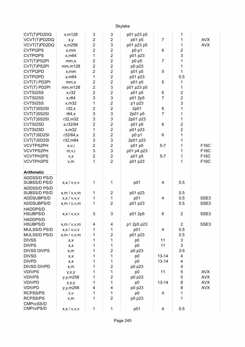
Skylake
Page 245
CVT(T)PD2DQ x,m128 3 3 p01 p23 p5 1VCVT(T)PD2DQ x,y 2 2 p01 p5 7 1 AVXVCVT(T)PD2DQ x,m256 2 3 p01 p23 p5 1 AVXCVTPI2PS x,mm 2 2 p0 p1 6 2CVTPI2PS x,m64 1 2 p01 p23 3CVT(T)PS2PI mm,x 2 2 p0 p5 7 1CVT(T)PS2PI mm,m128 2 2 p0 p23 1CVTPI2PD x,mm 2 2 p01 p5 5 1CVTPI2PD x,m64 1 2 p01 p23 0.5CVT(T) PD2PI mm,x 2 2 p01 p5 5 1CVT(T) PD2PI mm,m128 2 3 p01 p23 p5 1CVTSI2SS x,r32 2 2 p01 p5 6 2CVTSI2SS x,r64 3 3 p01 2p5 7 2CVTSI2SS x,m32 1 2 p1 p23 3CVT(T)SS2SI r32,x 2 2 2p01 6 1CVT(T)SS2SI r64,x 3 3 2p01 p5 7 1CVT(T)SS2SI r32,m32 3 3 2p01 p23 1CVTSI2SD x,r32/64 2 2 p01 p5 6 2CVTSI2SD x,m32 1 2 p01 p23 2CVT(T)SD2SI r32/64,x 2 2 p0 p1 6 1CVT(T)SD2SI r32,m64 3 3 2p01 p23 1VCVTPS2PH x,v,i 2 2 p01 p5 5-7 1 F16CVCVTPS2PH m,v,i 3 3 p01 p4 p23 1 F16CVCVTPH2PS v,x 2 2 p01 p5 5-7 1 F16CVCVTPH2PS v,m 1 2 p01 p23 1 F16C
Arithmetic
x,x / v,v,v 1 1 p01 4 0.5
x,m / v,v,m 1 2 p01 p23 0.5ADDSUBPS/D x,x / v,v,v 1 1 p01 4 0.5 SSE3ADDSUBPS/D x,m / v,v,m 1 2 p01 p23 0.5 SSE3
x,x / v,v,v 3 3 p01 2p5 6 2 SSE3
x,m / v,v,m 4 4 p1 2p5 p23 2 SSE3MULSS/D PS/D x,x / v,v,v 1 1 p01 4 0.5MULSS/D PS/D x,m / v,v,m 1 2 p01 p23 0.5DIVSS x,x 1 1 p0 11 3DIVPS x,x 1 1 p0 11 3DIVSS DIVPS x,m 1 2 p0 p23 3-5DIVSD x,x 1 1 p0 13-14 4DIVPD x,x 1 1 p0 13-14 4DIVSD DIVPD x,m 1 2 p0 p23 4VDIVPS y,y,y 1 1 p0 11 5 AVXVDIVPS y,y,m256 1 2 p0 p23 5 AVXVDIVPD y,y,y 1 1 p0 13-14 8 AVXVDIVPD y,y,m256 4 4 p0 p23 8 AVXRCPSS/PS v,v 1 1 p0 4 1RCPSS/PS v,m 1 2 p0 p23 1
x,x / v,v,v 1 1 p01 4 0.5
ADDSS/D PS/DSUBSS/D PS/DADDSS/D PS/DSUBSS/D PS/D
HADDPS/DHSUBPS/D
HADDPS/DHSUBPS/D
CMPccSS/D CMPccPS/D

Skylake
Page 246
x,m / v,v,m 2 2 p01 p23 0.5(U)COMISS/D x,x 1 1 p0 1(U)COMISS/D x,m32/64 2 2 p0 p23 1
x,x / v,v,v 1 1 p01 4 0.5
x,m / v,v,m 1 2 p01 p23 0.5
ROUNDSS/D PS/D v,v,i 2 2 2p01 8 1 SSE4.1
ROUNDSS/D PS/D v,m,i 3 3 2p01 p23 1 SSE4.1DPPS x,x,i / v,v,v,i 4 4 3p01 p5 13 1.5 SSE4.1DPPS x,m,i / v,v,m,i 6 6 3p01 p23 p5 p6 1.5 SSE4.1DPPD x,x,i 3 3 2p01 p5 9 1 SSE4.1DPPD x,m128,i 4 4 2p01 p23 p5 1 SSE4.1
v,v,v 1 1 p01 4 0.5 FMA
v,v,m 1 2 p01 p23 0.5 FMA
MathSQRTSS/PS x,x 1 1 p0 12 3SQRTSS/PS x,m128 1 2 p0 p23 3VSQRTPS y,y 1 1 p0 12 6 AVXVSQRTPS y,m256 4 4 p0 p23 6 AVXSQRTSD x,x 1 1 p0 15-16 4-6SQRTPD x,x 1 1 p0 15-16 4-6SQRTSD/PD x,m128 1 2 p0 p23 4-6VSQRTPD y,y 1 1 p0 15-16 9-12 AVXVSQRTPD y,m256 4 4 p0 p23 9-12 AVXRSQRTSS/PS v,v 1 1 p0 4 1RSQRTSS/PS v,m 1 2 p0 p23 1
Logic
x,x / v,v,v 1 1 p015 1 0.33
x,m / v,v,m 1 2 p015 p23 0.5
OtherVZEROUPPER 4 4 none 1 AVX
VZEROALL 25 25 p0 p1 p5 p6 12
VZEROALL 34 34 p0 p1 p5 p6 12LDMXCSR m32 4 4 p0 p5 p6 p23 5 3STMXCSR m32 3 4 p0 p4 p6 p237 5 2FXSAVE m4096 106 78 78 32 bit modeFXSAVE m4096 136 64 64 64 bit modeFXRSTOR m4096 105 76 76 32 bit modeFXRSTOR m4096 121 77 77 64 bit modeXSAVE 247 107 107 32 bit modeXSAVE 304 107 107 64 bit mode
CMPccSS/D CMPccPS/D
MAXSS/D PS/DMINSS/D PS/D
MAXSS/D PS/DMINSS/D PS/D
VFMADD...(all FMA instr.)
VFMADD...(all FMA instr.)
AND/ANDN/OR/XORPS/PD
AND/ANDN/OR/XORPS/PD
AVX,32 bit
AVX,64 bit
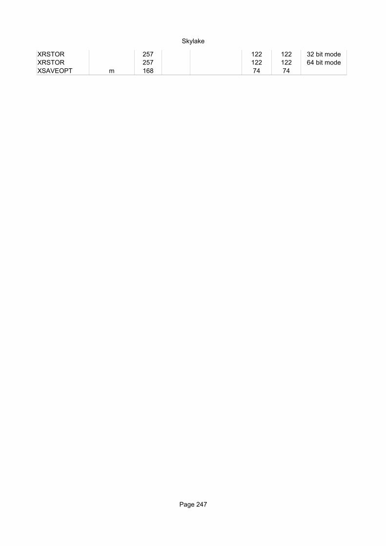
Skylake
Page 247
XRSTOR 257 122 122 32 bit modeXRSTOR 257 122 122 64 bit modeXSAVEOPT m 168 74 74

Pentium 4
Page 248
Intel Pentium 4List of instruction timings and μop breakdown
Explanation of column headings:Instruction:
Operands:
μops: Number of μops issued from instruction decoder and stored in trace cache.Microcode: Number of additional μops issued from microcode ROM.Latency:
Additional latency:
Port:
Execution unit:
Execution subunit:
Instruction set
Integer instructions
This list is measured for a Pentium 4, model 2. Timings for model 3 may be more like the values for P4E, listed on the next sheet
Instruction name. cc means any condition code. For example, Jcc can be JB, JNE, etc.
i = immediate constant, r = any register, r32 = 32-bit register, etc., mm = 64 bit mmx register, xmm = 128 bit xmm register, sr = segment register, m = any memory operand including indirect operands, m64 means 64-bit memory op-erand, etc.
This is the delay that the instruction generates in a dependency chain if the next dependent instruction starts in the same execution unit. The numbers are minimum values. Cache misses, misalignment, and exceptions may increase the clock counts considerably. Floating point operands are presumed to be normal numbers. Denormal numbers, NAN's, infinity and exceptions increase the delays. The latency of moves to and from memory cannot be measured accurately because of the problem with memory intermediates explained above under “How the values were measured”.
This number is added to the latency if the next dependent instruction is in a different execution unit. There is no additional latency between ALU0 and ALU1.
Reciprocalthroughput:
This is also called issue latency. This value indicates the number of clock cy-cles from the execution of an instruction begins to a subsequent independent instruction can begin to execute in the same execution subunit. A value of 0.25 indicates 4 instructions per clock cycle in one thread.
The port through which each μop goes to an execution unit. Two independent μops can start to execute simultaneously only if they are going through differ-ent ports.
Use this information to determine additional latency. When an instruction with more than one μop uses more than one execution unit, only the first and the last execution unit is listed.
Throughput measures apply only to instructions executing in the same sub-unit.
Indicates the compatibility of an instruction with other 80x86 family micropro-cessors. The instruction can execute on microprocessors that support the in-struction set indicated.

Pentium 4
Page 249
Instruction Operands
μo
ps
Mic
roc
od
e
La
ten
cy
Ad
ditio
na
l late
nc
y
Po
rt
Ex
ec
utio
n u
nit
Su
bu
nit
Ins
truc
tion
se
t
No
tes
Move instructionsMOV r,r 1 0 0,5 0.5-1 0,25 0/1 alu0/1 86 cMOV r,i 1 0 0,5 0.5-1 0,25 0/1 alu0/1 86MOV r32,m 1 0 2 0 1 2 load 86MOV r8/16,m 2 0 3 0 1 2 load 86MOV m,r 1 0 1 2 0 store 86 b, cMOV m,i 3 0 2 0,3 store 86MOV r,sr 4 2 6 86MOV sr,r/m 4 4 12 0 14 86 a, qMOVNTI m,r32 2 0 ≈33 sse2MOVZX r,r 1 0 0,5 0.5-1 0,25 0/1 alu0/1 386 cMOVZX r,m 1 0 2 0 1 2 load 386MOVSX r,r 1 0 0,5 0.5-1 0,5 0 alu0 386 cMOVSX r,m 2 0 3 0.5-1 1 2,0 386CMOVcc r,r/m 3 0 6 0 3 ppro a, eXCHG r,r 3 0 1,5 0.5-1 1 0/1 alu0/1 86XCHG r,m 4 8 >100 86XLAT 4 0 3 86PUSH r 2 0 1 2 86PUSH i 2 0 1 2 186PUSH m 3 0 2 86PUSH sr 4 4 7 86PUSHF(D) 4 4 10 86PUSHA(D) 4 10 19 186POP r 2 0 1 0 1 86POP m 4 8 14 86POP sr 4 5 13 86POPF(D) 4 8 52 86POPA(D) 4 16 14 186LEA r,[r+r/i] 1 0 0,5 0.5-1 0,25 0/1 alu0/1 86LEA r,[r+r+i] 2 0 1 0.5-1 0,5 0/1 alu0/1 86LEA r,[r*i] 3 0 4 0.5-1 1 1 int,alu 386LEA r,[r+r*i] 2 0 4 0.5-1 1 1 int,alu 386LEA r,[r+r*i+i] 3 0 4 0.5-1 1 1 int,alu 386LAHF 1 0 4 0 4 1 int 86SAHF 1 0 0,5 0.5-1 0,5 0/1 alu0/1 86 dSALC 3 0 5 0 1 1 int 86LDS, LES, ... r,m 4 7 15 86BSWAP r 3 0 7 0 2 int,alu 486IN, OUT r,r/i 8 64 >1000 86PREFETCHNTA m 4 2 6 ssePREFETCHT0/1/2 m 4 2 6 sse
Re
cipro
ca
l thro
ug
h-
pu
t

Pentium 4
Page 250
SFENCE 4 2 40 sseLFENCE 4 2 38 sse2MFENCE 4 2 100 sse2
Arithmetic instructionsADD, SUB r,r 1 0 0,5 0.5-1 0,25 0/1 alu0/1 86 cADD, SUB r,m 2 0 1 0.5-1 1 86 cADD, SUB m,r 3 0 ≥ 8 ≥ 4 86 cADC, SBB r,r 4 4 6 0 6 1 int,alu 86ADC, SBB r,i 3 0 6 0 6 1 int,alu 86ADC, SBB r,m 4 6 8 0 8 1 int,alu 86ADC, SBB m,r 4 7 ≥ 9 8 86CMP r,r 1 0 0,5 0.5-1 0,25 0/1 alu0/1 86 cCMP r,m 2 0 1 0.5-1 1 86 cINC, DEC r 2 0 0,5 0.5-1 0,5 0/1 alu0/1 86INC, DEC m 4 0 4 ≥ 4 86NEG r 1 0 0,5 0.5-1 0,5 0 alu0 86NEG m 3 0 ≥ 3 86AAA, AAS 4 27 90 86DAA, DAS 4 57 100 86AAD 4 10 22 1 int fpmul 86AAM 4 22 56 1 int fpdiv 86MUL, IMUL r8/32 4 6 16 0 8 1 int fpmul 86MUL, IMUL r16 4 7 17 0 8 1 int fpmul 86MUL, IMUL m8/32 4 7-8 16 0 8 1 int fpmul 86MUL, IMUL m16 4 10 16 0 8 1 int fpmul 86IMUL r32,r 4 0 14 0 4,5 1 int fpmul 386IMUL r32,(r),i 4 0 14 0 4,5 1 int fpmul 386IMUL r16,r 4 5 16 0 9 1 int fpmul 386IMUL r16,r,i 4 5 15 0 8 1 int fpmul 186IMUL r16,m16 4 7 15 0 10 1 int fpmul 386IMUL r32,m32 4 0 14 0 8 1 int fpmul 386IMUL r,m,i 4 7 14 0 10 1 int fpmul 186DIV r8/m8 4 20 61 0 24 1 int fpdiv 86 aDIV r16/m16 4 18 53 0 23 1 int fpdiv 86 aDIV r32/m32 4 21 50 0 23 1 int fpdiv 386IDIV r8/m8 4 24 61 0 24 1 int fpdiv 86 aIDIV r16/m16 4 22 53 0 23 1 int fpdiv 86 aIDIV r32/m32 4 20 50 0 23 1 int fpdiv 386 aCBW 2 0 1 0.5-1 1 0 alu0 86CWD, CDQ 2 0 1 0.5-1 0,5 0/1 alu0/1 86CWDE 1 0 0,5 0.5-1 0,5 0 alu0 386
Logic instructionsAND, OR, XOR r,r 1 0 0,5 0.5-1 0,5 0 alu0 86 cAND, OR, XOR r,m 2 0 ≥ 1 0.5-1 ≥ 1 86 cAND, OR, XOR m,r 3 0 ≥ 8 ≥ 4 86 cTEST r,r 1 0 0,5 0.5-1 0,5 0 alu0 86 cTEST r,m 2 0 ≥ 1 0.5-1 ≥ 1 86 cNOT r 1 0 0,5 0.5-1 0,5 0 alu0 86

Pentium 4
Page 251
NOT m 4 0 ≥ 4 86SHL, SHR, SAR r,i 1 0 4 1 1 1 int mmxsh 186SHL, SHR, SAR r,CL 2 0 6 0 1 1 int mmxsh 86 dROL, ROR r,i 1 0 4 1 1 1 int mmxsh 186 dROL, ROR r,CL 2 0 6 0 1 1 int mmxsh 86 dRCL, RCR r,1 1 0 4 1 1 1 int mmxsh 86 dRCL, RCR r,i 4 15 16 0 15 1 int mmxsh 186 dRCL, RCR r,CL 4 15 16 0 14 1 int mmxsh 86 d
m,i/CL 4 7-8 10 0 10 1 int mmxsh 86 dRCL, RCR m,1 4 7 10 0 10 1 int mmxsh 86 dRCL, RCR m,i/CL 4 18 18-28 14 1 int mmxsh 86 dSHLD, SHRD r,r,i/CL 4 14 14 0 14 1 int mmxsh 386SHLD, SHRD m,r,i/CL 4 18 14 0 14 1 int mmxsh 386BT r,i 3 0 4 0 2 1 int mmxsh 386 dBT r,r 2 0 4 0 1 1 int mmxsh 386 dBT m,i 4 0 4 0 2 1 int mmxsh 386 dBT m,r 4 12 12 0 12 1 int mmxsh 386 dBTR, BTS, BTC r,i 3 0 6 0 2 1 int mmxsh 386BTR, BTS, BTC r,r 2 0 6 0 4 1 int mmxsh 386BTR, BTS, BTC m,i 4 7 18 0 8 1 int mmxsh 386BTR, BTS, BTC m,r 4 15 14 0 14 1 int mmxsh 386BSF, BSR r,r 2 0 4 0 2 1 int mmxsh 386BSF, BSR r,m 3 0 4 0 3 1 int mmxsh 386SETcc r 3 0 5 0 1 1 int 386SETcc m 4 0 5 0 3 1 int 386CLC, STC 3 0 10 0 2 86 dCMC 3 0 10 0 2 86CLD 4 7 52 0 52 86STD 4 5 48 0 48 86CLI 4 5 35 35 86STI 4 12 43 43 86
Control transfer instructionsJMP short/near 1 0 0 0 1 0 alu0 branch 86JMP far 4 28 118 118 0 86JMP r 3 0 4 4 0 alu0 branch 86JMP m(near) 3 0 4 4 0 alu0 branch 86JMP m(far) 4 31 11 11 0 86Jcc short/near 1 0 0 2-4 0 alu0 branch 86J(E)CXZ short 4 4 0 2-4 0 alu0 branch 86LOOP short 4 4 0 2-4 0 alu0 branch 86CALL near 3 0 2 2 0 alu0 branch 86CALL far 4 34 0 86CALL r 4 4 8 0 alu0 branch 86CALL m(near) 4 4 9 0 alu0 branch 86CALL m(far) 4 38 0 86RETN 4 0 2 0 alu0 branch 86RETN i 4 0 2 0 alu0 branch 86RETF 4 33 11 0 86
SHL,SHR,SAR,ROL, ROR

Pentium 4
Page 252
RETF i 4 33 11 0 86IRET 4 48 24 0 86ENTER i,0 4 12 26 26 186ENTER i,n 4 45+24n 128+16n 186LEAVE 4 0 3 3 186BOUND m 4 14 14 14 186INTO 4 5 18 18 86INT i 4 84 644 86
String instructionsLODS 4 3 6 6 86REP LODS 4 5n ≈ 4n+36 86STOS 4 2 6 6 86REP STOS 4 2n+3 ≈ 3n+10 86MOVS 4 4 6 4 86REP MOVS 4 ≈163+1.1n 86SCAS 4 3 6 86REP SCAS 4 ≈ 40+6n ≈4n 86CMPS 4 5 8 86REP CMPS 4 ≈ 50+8n ≈4n 86
OtherNOP (90) 1 0 0 0,25 0/1 alu0/1 86Long NOP (0F 1F) 1 0 0 0,25 0/1 alu0/1 pproPAUSE 4 2 sse2CPUID 4 39-81 200-500 p5RDTSC 4 7 80 p5Notes:a) Add 1 μop if source is a memory operand.b)
c)
d) Has (false) dependence on the flags in most cases.e) Not available on PMMXq) Latency is 12 in 16-bit real or virtual mode, 24 in 32-bit protected mode.
Floating point x87 instructionsInstruction Operands
μo
ps
Mic
roc
od
e
La
ten
cy
Ad
ditio
na
l late
nc
y
Po
rt
Ex
ec
utio
n u
nit
Su
bu
nit
Ins
truc
tion
se
t
No
tes
Move instructionsFLD r 1 0 6 0 1 0 mov 87FLD m32/64 1 0 ≈ 7 0 1 2 load 87
Uses an extra μop (port 3) if SIB byte used. A SIB byte is needed if the mem-ory operand has more than one pointer register, or a scaled index, or ESP is used as base pointer.
Add 1 μop if source or destination, but not both, is a high 8-bit register (AH, BH, CH, DH).
Re
cipro
ca
l thro
ug
h-
pu
t

Pentium 4
Page 253
FLD m80 3 4 6 2 load 87FBLD m80 3 75 90 2 load 87FST(P) r 1 0 6 0 1 0 mov 87FST(P) m32/64 2 0 ≈ 7 2-3 0 store 87FSTP m80 3 8 8 0 store 87FBSTP m80 3 311 400 0 store 87FXCH r 1 0 0 0 1 0 mov 87FILD m16 3 3 ≈ 10 6 2 load 87FILD m32/64 2 0 ≈ 10 1 2 load 87FIST m16 3 0 ≈ 10 2-4 0 store 87FIST m32/64 2 0 ≈ 10 2-3 0 store 87FISTP m 3 0 ≈ 10 2-4 0 store 87FLDZ 1 0 2 0 mov 87FLD1 2 0 2 0 mov 87FCMOVcc st0,r 4 0 2-4 1 4 1 fp PPro eFFREE r 3 0 4 0 mov 87FINCSTP, FDECSTP 1 0 0 0 1 0 mov 87FNSTSW AX 4 0 11 0 3 1 287FSTSW AX 6 0 11 0 3 1 287FNSTSW m16 4 4 6 0 87FNSTCW m16 4 4 6 0 87FLDCW m16 4 7 (3) (8) 0,2 87 f
Arithmetic instructionsFADD(P),FSUB(R)(P) r 1 0 5 1 1 1 fp add 87FADD,FSUB(R) m 2 0 5 1 1 1 fp add 87FIADD,FISUB(R) m16 3 4 6 0 6 1 fp add 87FIADD,FISUB(R) m32 3 0 5 1 2 1 fp add 87FMUL(P) r 1 0 7 1 2 1 fp mul 87FMUL m 2 0 7 1 2 1 fp mul 87FIMUL m16 3 4 7 1 6 1 fp mul 87FIMUL m32 3 0 7 1 2 1 fp mul 87FDIV(R)(P) r 1 0 43 0 43 1 fp div 87 g, hFDIV(R) m 2 0 43 0 43 1 fp div 87 g, hFIDIV(R) m16 3 4 43 0 43 1 fp div 87 g, hFIDIV(R) m32 3 0 43 0 43 1 fp div 87 g, hFABS 1 0 2 1 1 1 fp misc 87FCHS 1 0 2 1 1 1 fp misc 87FCOM(P), FUCOM(P) r 1 0 2 0 1 1 fp misc 87FCOM(P) m 2 0 2 0 1 1 fp misc 87FCOMPP, FUCOMPP 2 0 2 0 1 1 fp misc 87FCOMI(P) r 3 0 10 0 3 0,1 fp misc PProFICOM(P) m16 4 4 6 1 fp misc 87FICOM(P) m32 3 0 2 0 2 1,2 fp misc 87FTST 1 0 2 0 1 1 fp misc 87FXAM 1 0 2 0 1 1 fp misc 87FRNDINT 3 15 23 0 15 0,1 87FPREM 6 84 212 1 fp 87FPREM1 6 84 212 1 fp 387
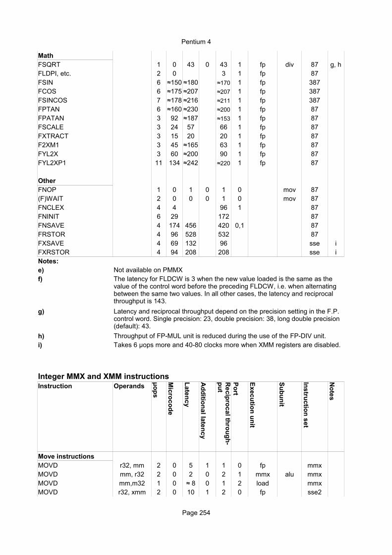
Pentium 4
Page 254
MathFSQRT 1 0 43 0 43 1 fp div 87 g, hFLDPI, etc. 2 0 3 1 fp 87FSIN 6 ≈150 ≈180 ≈170 1 fp 387FCOS 6 ≈175 ≈207 ≈207 1 fp 387FSINCOS 7 ≈178 ≈216 ≈211 1 fp 387FPTAN 6 ≈160 ≈230 ≈200 1 fp 87FPATAN 3 92 ≈187 ≈153 1 fp 87FSCALE 3 24 57 66 1 fp 87FXTRACT 3 15 20 20 1 fp 87F2XM1 3 45 ≈165 63 1 fp 87FYL2X 3 60 ≈200 90 1 fp 87FYL2XP1 11 134 ≈242 ≈220 1 fp 87
OtherFNOP 1 0 1 0 1 0 mov 87(F)WAIT 2 0 0 0 1 0 mov 87FNCLEX 4 4 96 1 87FNINIT 6 29 172 87FNSAVE 4 174 456 420 0,1 87FRSTOR 4 96 528 532 87FXSAVE 4 69 132 96 sse iFXRSTOR 4 94 208 208 sse iNotes:e) Not available on PMMXf)
g)
h) Throughput of FP-MUL unit is reduced during the use of the FP-DIV unit.i) Takes 6 μops more and 40-80 clocks more when XMM registers are disabled.
Integer MMX and XMM instructionsInstruction Operands
μo
ps
Mic
roc
od
e
La
ten
cy
Ad
ditio
na
l late
nc
y
Po
rt
Ex
ec
utio
n u
nit
Su
bu
nit
Ins
truc
tion
se
t
No
tes
Move instructionsMOVD r32, mm 2 0 5 1 1 0 fp mmxMOVD mm, r32 2 0 2 0 2 1 mmx alu mmxMOVD mm,m32 1 0 ≈ 8 0 1 2 load mmxMOVD r32, xmm 2 0 10 1 2 0 fp sse2
The latency for FLDCW is 3 when the new value loaded is the same as the value of the control word before the preceding FLDCW, i.e. when alternating between the same two values. In all other cases, the latency and reciprocal throughput is 143.
Latency and reciprocal throughput depend on the precision setting in the F.P. control word. Single precision: 23, double precision: 38, long double precision (default): 43.
Re
cipro
ca
l thro
ug
h-
pu
t

Pentium 4
Page 255
MOVD xmm, r32 2 0 6 1 2 1 mmx shift sse2MOVD xmm,m32 1 0 ≈ 8 0 1 2 load sse2MOVD m32, r 2 0 ≈ 8 2 0,1 mmxMOVQ mm,mm 1 0 6 0 1 0 mov mmxMOVQ xmm,xmm 1 0 2 1 2 1 mmx shift sse2MOVQ r,m64 1 0 ≈ 8 1 2 load mmxMOVQ m64,r 2 0 ≈ 8 2 0 mov mmxMOVDQA xmm,xmm 1 0 6 0 1 0 mov sse2MOVDQA xmm,m 1 0 ≈ 8 1 2 load sse2MOVDQA m,xmm 2 0 ≈ 8 2 0 mov sse2MOVDQU xmm,m 4 0 2 2 load sse2 kMOVDQU m,xmm 4 6 2 0 mov sse2 kMOVDQ2Q mm,xmm 3 0 8 1 2 0,1 mov-mmx sse2MOVQ2DQ xmm,mm 2 0 8 1 2 0,1 mov-mmx sse2MOVNTQ m,mm 3 0 75 0 mov sseMOVNTDQ m,xmm 2 0 18 0 mov sse2
mm,r/m 1 0 2 1 1 1 mmx shift mmx a
xmm,r/m 1 0 4 1 2 1 mmx shift mmx a
mm,r/m 1 0 2 1 1 1 mmx shift mmx a
xmm,r/m 1 0 4 1 2 1 mmx shift sse2 a
xmm,r/m 1 0 2 1 2 1 mmx shift sse2 aPSHUFD xmm,xmm,i 1 0 4 1 2 1 mmx shift sse2PSHUFL/HW xmm,xmm,i 1 0 2 1 2 1 mmx shift sse2PSHUFW mm,mm,i 1 0 2 1 1 1 mmx shift mmxMASKMOVQ mm,mm 4 4 7 0 mov sseMASKMOVDQU xmm,xmm 4 6 10 0 mov sse2PMOVMSKB r32,r 2 0 7 1 3 0,1 mmx-alu0 ssePEXTRW r32,mm,i 3 0 8 1 2 1 mmx-int ssePEXTRW r32,xmm,i 3 0 9 1 2 1 mmx-int sse2PINSRW mm,r32,i 2 0 3 1 2 1 int-mmx ssePINSRW xmm,r32,i 2 0 4 1 2 1 int-mmx sse2
Arithmetic instructions
r,r/m 1 0 2 1 1,2 1 mmx alu mmx a,j
r,r/m 1 0 2 1 1,2 1 mmx alu mmx a,jPADDQ, PSUBQ mm,r/m 1 0 2 1 1 1 mmx alu sse2 aPADDQ, PSUBQ xmm,r/m 1 0 4 1 2 1 fp add sse2 a
r,r/m 1 0 2 1 1,2 1 mmx alu mmx a,jPMULLW PMULHW r,r/m 1 0 6 1 1,2 1 fp mul mmx a,jPMULHUW r,r/m 1 0 6 1 1,2 1 fp mul sse a,jPMADDWD r,r/m 1 0 6 1 1,2 1 fp mul mmx a,jPMULUDQ r,r/m 1 0 6 1 1,2 1 fp mul sse2 a,jPAVGB/W r,r/m 1 0 2 1 1,2 1 mmx alu sse a,j
PACKSSWB/DW PACKUSWB
PACKSSWB/DW PACKUSWB
PUNPCKH/LBW/WD/ DQ
PUNPCKHBW/WD/DQ/QDQ
PUNPCKLBW/WD/DQ/QDQ
PADDB/W/D PADD(U)SB/W
PSUBB/W/D PSUB(U)SB/W
PCMPEQB/W/D PCMPGTB/W/D

Pentium 4
Page 256
PMIN/MAXUB r,r/m 1 0 2 1 1,2 1 mmx alu sse a,jPMIN/MAXSW r,r/m 1 0 2 1 1,2 1 mmx alu sse a,jPSADBW r,r/m 1 0 4 1 1,2 1 mmx alu sse a,j
LogicPAND, PANDN r,r/m 1 0 2 1 1,2 1 mmx alu mmx a,jPOR, PXOR r,r/m 1 0 2 1 1,2 1 mmx alu mmx a,j
r,i/r/m 1 0 2 1 1,2 1 mmx shift mmx a,jPSLLDQ, PSRLDQ xmm,i 1 0 4 1 2 1 mmx shift sse2 a
OtherEMMS 4 11 12 12 0 mmxNotes:a) Add 1 μop if source is a memory operand.j) Reciprocal throughput is 1 for 64 bit operands, and 2 for 128 bit operands.k) It may be advantageous to replace this instruction by two 64-bit moves
Floating point XMM instructionsInstruction Operands
μo
ps
Mic
roc
od
e
La
ten
cy
Ad
ditio
na
l late
nc
y
Po
rt
Ex
ec
utio
n u
nit
Su
bu
nit
Ins
truc
tion
se
t
No
tes
Move instructionsMOVAPS/D r,r 1 0 6 0 1 0 mov sseMOVAPS/D r,m 1 0 ≈ 7 0 1 2 sseMOVAPS/D m,r 2 0 ≈ 7 2 0 sseMOVUPS/D r,r 1 0 6 0 1 0 mov sseMOVUPS/D r,m 4 0 2 2 sse kMOVUPS/D m,r 4 6 8 0 sse kMOVSS r,r 1 0 2 0 2 1 mmx shift sseMOVSD r,r 1 0 2 1 2 1 mmx shift sseMOVSS, MOVSD r,m 1 0 ≈ 7 0 1 2 sseMOVSS, MOVSD m,r 2 0 2 0 sseMOVHLPS r,r 1 0 4 0 2 1 mmx shift sseMOVLHPS r,r 1 0 2 0 2 1 mmx shift sseMOVHPS/D, MOVLPS/D
r,m 3 0 4 2 sseMOVHPS/D, MOVLPS/D
m,r 2 0 2 0 sseMOVNTPS/D m,r 2 0 4 0 sse/2MOVMSKPS/D r32,r 2 0 6 1 3 1 fp sseSHUFPS/D r,r/m,i 1 0 4 1 2 1 mmx shift sseUNPCKHPS/D r,r/m 1 0 4 1 2 1 mmx shift sseUNPCKLPS/D r,r/m 1 0 2 1 2 1 mmx shift sse
PSLL/RLW/D/Q, PSRAW/D
Re
cipro
ca
l thro
ug
h-
pu
t

Pentium 4
Page 257
ConversionCVTPS2PD r,r/m 4 0 7 1 4 1 mmx shift sse2 aCVTPD2PS r,r/m 2 0 10 1 2 1 fp-mmx sse2 aCVTSD2SS r,r/m 4 0 14 1 6 1 mmx shift sse2 aCVTSS2SD r,r/m 4 0 10 1 6 1 mmx shift sse2 aCVTDQ2PS r,r/m 1 0 4 1 2 1 fp sse2 aCVTDQ2PD r,r/m 3 0 9 1 4 1 mmx-fp sse2 aCVT(T)PS2DQ r,r/m 1 0 4 1 2 1 fp sse2 aCVT(T)PD2DQ r,r/m 2 0 9 1 2 1 fp-mmx sse2 aCVTPI2PS xmm,mm 4 0 10 1 4 1 mmx sse aCVTPI2PD xmm,mm 4 0 11 1 5 1 fp-mmx sse2 aCVT(T)PS2PI mm,xmm 3 0 7 0 2 0,1 fp-mmx sse aCVT(T)PD2PI mm,xmm 3 0 11 1 3 0,1 fp-mmx sse2 aCVTSI2SS xmm,r32 3 0 10 1 3 1 fp-mmx sse aCVTSI2SD xmm,r32 4 0 15 1 6 1 fp-mmx sse2 aCVT(T)SD2SI r32,xmm 2 0 8 1 2,5 1 fp sse2 aCVT(T)SS2SI r32,xmm 2 0 8 1 2,5 1 fp sse a
ArithmeticADDPS/D ADDSS/D r,r/m 1 0 4 1 2 1 fp add sse aSUBPS/D SUBSS/D r,r/m 1 0 4 1 2 1 fp add sse aMULPS/D MULSS/D r,r/m 1 0 6 1 2 1 fp mul sse aDIVSS r,r/m 1 0 23 0 23 1 fp div sse a,hDIVPS r,r/m 1 0 39 0 39 1 fp div sse a,hDIVSD r,r/m 1 0 38 0 38 1 fp div sse2 a,hDIVPD r,r/m 1 0 69 0 69 1 fp div sse2 a,hRCPPS RCPSS r,r/m 2 0 4 1 4 1 mmx sse a
r,r/m 1 0 4 1 2 1 fp add sse a
r,r/m 1 0 4 1 2 1 fp add sse aCOMISS/D UCOMISS/D r,r/m 2 0 6 1 3 1 fp add sse a
Logic
r,r/m 1 0 2 1 2 1 mmx alu sse a
MathSQRTSS r,r/m 1 0 23 0 23 1 fp div sse a,hSQRTPS r,r/m 1 0 39 0 39 1 fp div sse a,hSQRTSD r,r/m 1 0 38 0 38 1 fp div sse2 a,hSQRTPD r,r/m 1 0 69 0 69 1 fp div sse2 a,hRSQRTSS r,r/m 2 0 4 1 3 1 mmx sse aRSQRTPS r,r/m 2 0 4 1 4 1 mmx sse a
OtherLDMXCSR m 4 8 98 100 1 sseSTMXCSR m 4 4 6 1 sseNotes:
MAXPS/D MAXSS/DMINPS/D MINSS/D
CMPccPS/DCMPccSS/D
ANDPS/D ANDNPS/D ORPS/D XORPS/D

Pentium 4
Page 258
a) Add 1 μop if source is a memory operand.h) Throughput of FP-MUL unit is reduced during the use of the FP-DIV unit.k) It may be advantageous to replace this instruction by two 64-bit moves.

Prescott
Page 259
Intel Pentium 4 w. EM64T (Prescott)List of instruction timings and μop breakdown
Explanation of column headings:Instruction:
Operands:
μops: Number of μops issued from instruction decoder and stored in trace cache.Microcode: Number of additional μops issued from microcode ROM.Latency:
Additional latency:
Port:
Execution unit:
Execution subunit: Throughput measures apply only to instructions executing in the same subunit.Instruction set
Integer instructionsInstruction Operands
μo
ps
Mic
roc
od
e
La
ten
cy
Ad
ditio
na
l late
nc
y
Po
rt
Ex
ec
utio
n u
nit
Su
bu
nit
Ins
truc
tion
se
t
No
tes
Move instructionsMOV r,r 1 0 1 0 0,25 0/1 alu0/1 86 cMOV r8/16/32,i 1 0 1 0 0,25 0/1 alu0/1 86MOV r64,i32 1 0 0 0,5 0/1 alu0/1 x64
Instruction name. cc means any condition code. For example, Jcc can be JB, JNE, etc.
i = immediate constant, r = any register, r32 = 32-bit register, etc., mm = 64 bit mmx register, xmm = 128 bit xmm register, sr = segment register, m = any memory operand including indirect operands, m64 means 64-bit memory oper-and, etc., mabs = memory operand with 64-bit absolute address.
This is the delay that the instruction generates in a dependency chain if the next dependent instruction starts in the same execution unit. The numbers are mini-mum values. Cache misses, misalignment, and exceptions may increase the clock counts considerably. Floating point operands are presumed to be normal numbers. Denormal numbers, NAN's, infinity and exceptions increase the de-lays. The latency of moves to and from memory cannot be measured accurately because of the problem with memory intermediates explained above under “How the values were measured”.
This number is added to the latency if the next dependent instruction is in a dif-ferent execution unit. There is no additional latency between ALU0 and ALU1.
Reciprocalthroughput:
This is also called issue latency. This value indicates the number of clock cycles from the execution of an instruction begins to a subsequent independent in-struction can begin to execute in the same execution subunit. A value of 0.25 indicates 4 instructions per clock cycle in one thread.
The port through which each μop goes to an execution unit. Two independent μops can start to execute simultaneously only if they are going through different ports.
Use this information to determine additional latency. When an instruction with more than one μop uses more than one execution unit, only the first and the last execution unit is listed.
Indicates the compatibility of an instruction with other 80x86 family micropro-cessors. The instruction can execute on microprocessors that support the in-struction set indicated.
Re
cip
roc
al th
rou
gh
-p
ut

Prescott
Page 260
MOV r64,i64 2 0 0 1 1 alu1 x64MOV r8/16,m 2 0 3 0 1 2 load 86MOV r32/64,m 1 0 2 0 1 2 load 86MOV m,r 1 0 2 0 store 86 b,cMOV m,i 2 0 2 0,3 store 86MOV m64,i32 2 0 2 0,3 store x64MOV r,sr 1 2 8 86MOV sr,r/m 1 8 27 86 a,qMOV r,mabs 3 0 1 x64 lMOV mabs,r 3 0 2 x64 lMOVNTI m,r32 2 0 2 sse2MOVZX r,r 1 0 1 0 0,25 0/1 alu0/1 386 cMOVZX r16,r8 2 0 2 0 1 0/1 alu0/1 386 cMOVZX r,m 1 0 2 0 1 2 load 386MOVSX r16,r8 2 0 2 0 1 0 alu0 386 a,c,oMOVSX r32/64,r8/16 1 0 1 0 0,5 0 alu0 386 a,c,oMOVSX r,m 2 0 3 0 1 2 load 386MOVSXD r64,r32 1 0 1 0 0,5 0 alu0 x64 aCMOVcc r,r/m 3 0 9,5 0 3 PPro a,eXCHG r,r 3 0 2 0 1 0/1 alu0/1 86XCHG r,m 2 6 ≈100 86XLAT 4 0 6 86PUSH r 2 0 2 2 86PUSH i 2 0 2 2 186PUSH m 3 0 2 2 86PUSH sr 1 3 9 86PUSHF(D/Q) 1 3 9 86PUSHA(D) 1 9 16 186 mPOP r 2 0 1 0 1 86POP m 2 6 10 86POP sr 1 8 30 86POPF(D/Q) 1 8 70 86POPA(D) 2 16 15 186 mLEA r,[m] 1 0 0,25 0/1 alu0/1 86 pLEA r,[r+r/i] 1 0 2,5 0 0,25 0/1 alu0/1 86LEA r,[r+r+i] 2 0 3,5 0 0,5 0/1 alu0/1 86LEA r,[r*i] 3 0 3,5 0 1 1 alu 386LEA r,[r+r*i] 2 0 3,5 0 1 0,1 alu0,1 386LEA r,[r+r*i+i] 3 0 3,5 0 1 1 alu 386LAHF 1 0 4 0 1 int 86 nSAHF 1 0 5 0 0/1 alu0/1 86 d,nSALC 2 0 0 1 1 int 86 mLDS, LES, ... r,m 2 10 28 86 mLODS 1 3 8 8 86REP LODS 1 5n ≈ 4n+50 86STOS 1 2 8 8 86REP STOS 1 2.5n ≈ 3n 86MOVS 1 4 8 8 86REP MOVSB 9 ≈.3n ≈.3n 86REP MOVSW 1 ≈.5-1.1n≈ .6-1.4n 86

Prescott
Page 261
REP MOVSD 1 ≈1.1n ≈ 1.4 n 86REP MOVSQ 1 ≈1.1n ≈ 1.4 n x64BSWAP r 1 0 1 0 1 alu 486IN, OUT r,r/i 1 52 >1000 86PREFETCHNTA m 1 0 1 ssePREFETCHT0/1/2 m 1 0 1 sseSFENCE 1 2 50 sseLFENCE 1 2 50 sse2MFENCE 1 4 124 sse2
Arithmetic instructionsADD, SUB r,r 1 0 1 0 0,25 0/1 alu0/1 86 cADD, SUB r,m 2 0 1 0 1 86 cADD, SUB m,r 3 0 5 2 86 cADC, SBB r,r/i 3 0 10 0 10 1 int,alu 86ADC, SBB r,m 2 5 10 0 10 1 int,alu 86ADC, SBB m,r 2 6 20 10 86ADC, SBB m,i 3 5 22 10 86CMP r,r 1 0 1 0 0,25 0/1 alu0/1 86 cCMP r,m 2 0 1 0 1 86 cINC, DEC r 2 0 1 0 0,5 0/1 alu0/1 86INC, DEC m 4 0 5 3 86NEG r 1 0 1 0 0,5 0 alu0 86NEG m 3 0 5 3 86AAA, AAS 1 10 26 86 mDAA, DAS 1 16 29 86 mAAD 2 5 13 1 int mul 86 mAAM 2 17 71 1 int fpdiv 86 mMUL, IMUL r8 1 0 10 0 1 int mul 86MUL, IMUL r16 4 0 11 0 1 int mul 86MUL, IMUL r32 3 0 11 0 1 int mul 86MUL, IMUL r64 1 5 11 0 1 int mul x64MUL, IMUL m8 2 0 10 0 1 int mul 86MUL, IMUL m16 2 5 11 0 1 int mul 86MUL, IMUL m32 3 0 11 0 1 int mul 86MUL, IMUL m64 2 6 11 0 1 int mul x64IMUL r16,r16 1 0 10 0 2,5 1 int mul 386IMUL r16,r16,i 2 0 11 0 2,5 1 int mul 186IMUL r32,r32 1 0 10 0 2,5 1 int mul 386IMUL r32,(r32),i 1 0 10 0 2,5 1 int mul 386IMUL r64,r64 1 0 10 0 2,5 1 int mul x64IMUL r64,(r64),i 1 0 10 0 2,5 1 int mul x64IMUL r16,m16 2 0 10 0 2,5 1 int mul 386IMUL r32,m32 2 0 10 0 2,5 1 int mul 386IMUL r64,m64 2 0 10 0 2,5 1 int mul x64IMUL r,m,i 3 0 10 0 1-2.5 1 int mul 186DIV r8/m8 1 20 74 0 34 1 int fpdiv 86 aDIV r16/m16 1 19 73 0 34 1 int fpdiv 86 aDIV r32/m32 1 21 76 0 34 1 int fpdiv 386 aDIV r64/m64 1 31 63 0 52 1 int fpdiv x64 a

Prescott
Page 262
IDIV r8/m8 1 21 76 0 34 1 int fpdiv 86 aIDIV r16/m16 1 19 79 0 34 1 int fpdiv 86 aIDIV r32/m32 1 19 79 0 34 1 int fpdiv 386 aIDIV r64/m64 1 58 96 0 91 1 int fpdiv x64 aCBW 2 0 2 0 1 0 alu0 86CWD 2 0 2 0 1 0/1 alu0/1 86CDQ 1 0 1 0 1 0/1 alu0/1 386CQO 1 0 7 0 1 0/1 alu0/1 x64CWDE 2 0 2 0 1 0/1 alu0/1 386CDQE 1 0 1 0 1 0/1 alu0/1 x64SCAS 1 3 0 8 86REP SCAS 1 ≈ 54+6n ≈ 4n 86CMPS 1 5 10 86REP CMPS 1 ≈ 81+8n ≈ 5n 86
LogicAND, OR, XOR r,r 1 0 1 0 0,5 0 alu0 86 cAND, OR, XOR r,m 2 0 1 0 1 86 cAND, OR, XOR m,r 3 0 5 2 86 cTEST r,r 1 0 1 0 0,5 0 alu0 86 cTEST r,m 2 0 1 0 1 86 cNOT r 1 0 1 0 0,5 0 alu0 86NOT m 3 0 5 2 86SHL r,i 1 0 1 0 0,5 1 alu1 186SHR, SAR r8/16/32,i 1 0 1 0 0,5 1 alu1 186SHR, SAR r64,i 1 0 7 0 2 1 alu1 x64SHL r,CL 2 0 2 0 2 1 alu1 86SHR, SAR r8/16/32,CL 2 0 2 0 2 1 alu1 86SHR, SAR r64,CL 2 0 8 0 1 alu1 x64ROL, ROR r8/16/32,i 1 0 1 0 1 1 alu1 186 dROL, ROR r64,i 1 0 7 0 7 1 alu1 x64 dROL, ROR r8/16/32,CL 2 0 2 0 2 1 alu1 86 dROL, ROR r64,CL 2 0 8 0 8 1 alu1 x64 dRCL, RCR r,1 1 0 7 0 7 1 alu1 86 dRCL r,i 2 11 31 0 31 1 alu1 186 dRCR r,i 2 11 25 0 25 1 alu1 186 dRCL r,CL 1 11 31 0 31 1 alu1 86 dRCR r,CL 1 11 25 0 25 1 alu1 86 dSHL, SHR, SAR m8/16/32,i 3 6 10 0 1 alu1 86ROL. ROR m8/16/32,i 3 6 10 0 1 alu1 86 dSHL, SHR, SAR m8/16/32,cl 2 6 10 0 1 alu1 86ROL. ROR m8/16/32,cl 2 6 10 0 1 alu1 86 dRCL, RCR m8/16/32,1 2 5 27 0 27 1 alu1 86 dRCL, RCR m8/16/32,i 3 13 38 0 38 1 alu1 86 dRCL, RCR m8/16/32,cl 2 13 37 0 37 1 alu1 86 dSHLD, SHRD r8/16/32,r,i 3 0 8 0 7 1 alu1 386SHLD r64,r64,i 4 5 10 0 1 alu1 x64SHRD r64,r64,i 3 7 10 0 1 alu1 x64SHLD, SHRD r8/16/32,r,cl 4 0 9 0 8 1 alu1 386SHLD r64,r64,cl 4 5 14 0 1 alu1 x64

Prescott
Page 263
SHRD r64,r64,cl 3 8 12 0 1 alu1 x64SHLD, SHRD m,r,i 3 8 20 0 10 1 alu1 386SHLD, SHRD m,r,CL 2 8 20 0 10 1 alu1 386BT r,i 1 0 8 0 8 1 alu1 386 dBT r,r 2 0 9 0 9 1 alu1 386 dBT m,i 3 0 8 0 8 1 alu1 386 dBT m,r 2 7 10 0 10 1 alu1 386 dBTR, BTS, BTC r,i 1 0 8 0 8 1 alu1 386BTR, BTS, BTC r,r 2 0 9 0 9 1 alu1 386BTR, BTS, BTC m,i 3 6 28 0 10 1 alu1 386BTR, BTS, BTC m,r 2 10 14 0 14 1 alu1 386BSF, BSR r,r/m 2 0 16 0 4 1 alu1 386SETcc r 2 0 9 0 1 1 int 386SETcc m 3 0 9 0 2 1 int 386CLC, STC 2 0 0 8 86 dCMC 3 0 15 0 86CLD, STD 1 8 0 53 86
Control transfer instructionsJMP short/near 1 0 0 0 1 0 alu0 branch 86JMP far 2 25 154 0 86 mJMP r 3 0 15 0 alu0 branch 86JMP m(near) 3 0 10 0 alu0 branch 86JMP m(far) 2 28 157 0 86Jcc short/near 1 0 2-4 0 alu0 branch 86J(E)CXZ short 4 0 4 0 alu0 branch 86LOOP short 4 0 4 0 alu0 branch 86CALL near 3 0 7 0 alu0 branch 86CALL far 3 29 160 0 86 mCALL r 4 0 7 0 alu0 branch 86CALL m(near) 4 0 9 0 alu0 branch 86CALL m(far) 2 32 160 0 86RETN 4 0 7 0 alu0 branch 86RETN i 4 0 7 0 alu0 branch 86RETF 1 30 160 0 86RETF i 2 30 160 0 86IRET 1 49 325 0 86BOUND m 2 11 12 186 mINT i 2 67 470 86INTO 1 4 26 86 m
OtherNOP (90) 1 0 0 0,25 0/1 alu0/1 86Long NOP (0F 1F) 1 0 0 0,25 0/1 alu0/1 pproPAUSE 1 2 50 sse2LEAVE 4 0 5 5 186CLI 1 5 52 86STI 1 11 64 86CPUID 1 49-90 300-500 p5RDTSC 1 12 100 p5

Prescott
Page 264
RDPMC (bit 31 = 1) 1 37 100 p5RDPMC (bit 31 = 0) 4 154 240 p5MONITOR (sse3)MWAIT (sse3)Notes:a) Add 1 μop if source is a memory operand.b) Uses an extra μop (port 3) if SIB byte used.c)
d) Has (false) dependence on the flags in most cases.e) Not available on PMMXl)
m) Not available in 64 bit mode.n) Not available in 64 bit mode on some processors.o)
p)
q)
Floating point x87 instructionsInstruction Operands
μo
ps
Mic
roc
od
e
La
ten
cy
Ad
ditio
na
l late
nc
y
Po
rt
Ex
ec
utio
n u
nit
Su
bu
nit
Ins
truc
tion
se
t
No
tes
Move instructionsFLD r 1 0 7 0 1 0 mov 87FLD m32/64 1 0 0 1 2 load 87FLD m80 3 3 8 2 load 87FBLD m80 3 74 90 2 load 87FST(P) r 1 0 7 0 1 0 mov 87FST(P) m32/64 2 0 7 2 0 store 87FSTP m80 3 6 10 0 store 87FBSTP m80 3 311 400 0 store 87FXCH r 1 0 0 0 1 0 mov 87FILD m16 3 2 8 2 load 87FILD m32/64 2 0 2 2 load 87FIST(P) m 3 0 2,5 0 store 87FISTTP m 3 0 2,5 0 store sse3FLDZ 1 0 2 0 mov 87
Add 1 μop if source or destination, but not both, is a high 8-bit register (AH, BH, CH, DH).
Move accumulator to/from memory with 64 bit absolute address (opcode A0 - A3).
MOVSX uses an extra μop if the destination register is smaller than the biggest register size available. Use a 32 bit destination register in 16 bit and 32 bit mode, and a 64 bit destination register in 64 bit mode for optimal performance.
LEA with a direct memory operand has 1 μop and a reciprocal throughput of 0.25. This also applies if there is a RIP-relative address in 64-bit mode. A sign-extended 32-bit direct memory operand in 64-bit mode without RIP-relative ad-dress takes 2 μops because of the SIB byte. The throughput is 1 in this case. You may use a MOV instead.
These values are measured in 32-bit mode. In 16-bit real mode there is 1 mi-crocode μop and a reciprocal throughput of 17.
Re
cip
roc
al th
rou
gh
-p
ut
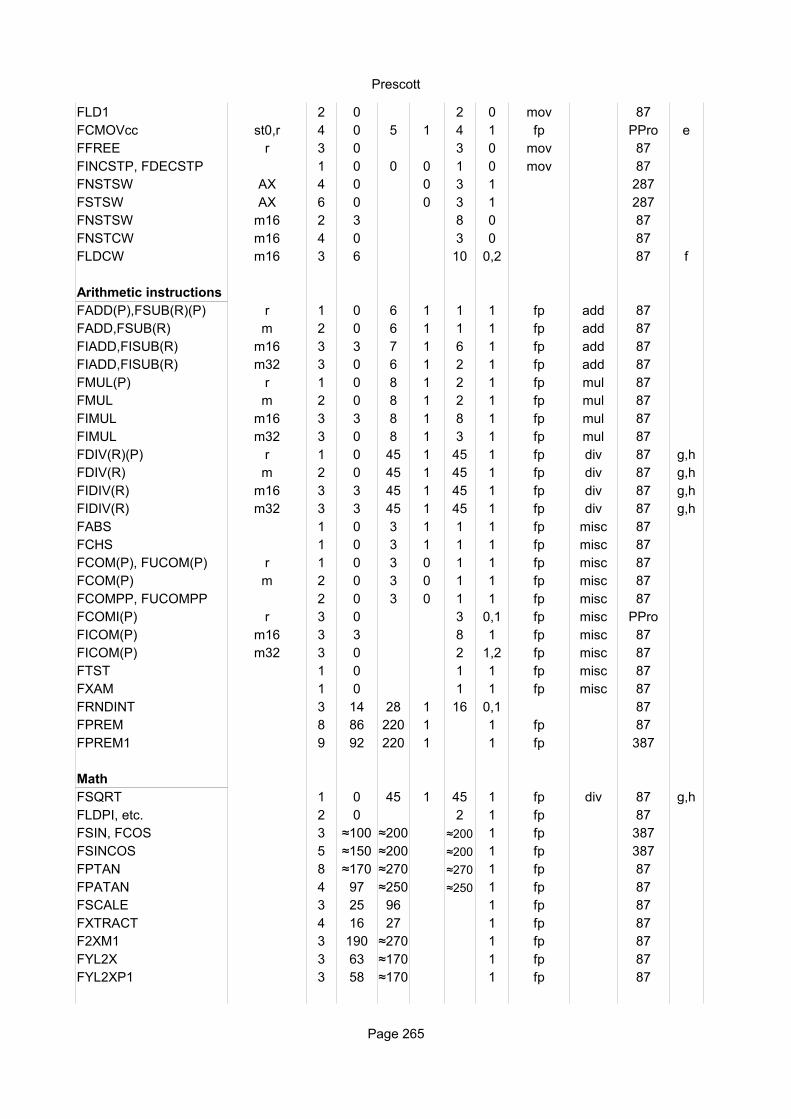
Prescott
Page 265
FLD1 2 0 2 0 mov 87FCMOVcc st0,r 4 0 5 1 4 1 fp PPro eFFREE r 3 0 3 0 mov 87FINCSTP, FDECSTP 1 0 0 0 1 0 mov 87FNSTSW AX 4 0 0 3 1 287FSTSW AX 6 0 0 3 1 287FNSTSW m16 2 3 8 0 87FNSTCW m16 4 0 3 0 87FLDCW m16 3 6 10 0,2 87 f
Arithmetic instructionsFADD(P),FSUB(R)(P) r 1 0 6 1 1 1 fp add 87FADD,FSUB(R) m 2 0 6 1 1 1 fp add 87FIADD,FISUB(R) m16 3 3 7 1 6 1 fp add 87FIADD,FISUB(R) m32 3 0 6 1 2 1 fp add 87FMUL(P) r 1 0 8 1 2 1 fp mul 87FMUL m 2 0 8 1 2 1 fp mul 87FIMUL m16 3 3 8 1 8 1 fp mul 87FIMUL m32 3 0 8 1 3 1 fp mul 87FDIV(R)(P) r 1 0 45 1 45 1 fp div 87 g,hFDIV(R) m 2 0 45 1 45 1 fp div 87 g,hFIDIV(R) m16 3 3 45 1 45 1 fp div 87 g,hFIDIV(R) m32 3 3 45 1 45 1 fp div 87 g,hFABS 1 0 3 1 1 1 fp misc 87FCHS 1 0 3 1 1 1 fp misc 87FCOM(P), FUCOM(P) r 1 0 3 0 1 1 fp misc 87FCOM(P) m 2 0 3 0 1 1 fp misc 87FCOMPP, FUCOMPP 2 0 3 0 1 1 fp misc 87FCOMI(P) r 3 0 3 0,1 fp misc PProFICOM(P) m16 3 3 8 1 fp misc 87FICOM(P) m32 3 0 2 1,2 fp misc 87FTST 1 0 1 1 fp misc 87FXAM 1 0 1 1 fp misc 87FRNDINT 3 14 28 1 16 0,1 87FPREM 8 86 220 1 1 fp 87FPREM1 9 92 220 1 1 fp 387
MathFSQRT 1 0 45 1 45 1 fp div 87 g,hFLDPI, etc. 2 0 2 1 fp 87FSIN, FCOS 3 ≈100 ≈200 ≈200 1 fp 387FSINCOS 5 ≈150 ≈200 ≈200 1 fp 387FPTAN 8 ≈170 ≈270 ≈270 1 fp 87FPATAN 4 97 ≈250 ≈250 1 fp 87FSCALE 3 25 96 1 fp 87FXTRACT 4 16 27 1 fp 87F2XM1 3 190 ≈270 1 fp 87FYL2X 3 63 ≈170 1 fp 87FYL2XP1 3 58 ≈170 1 fp 87

Prescott
Page 266
OtherFNOP 1 0 1 0 1 0 mov 87(F)WAIT 2 0 0 0 1 0 mov 87FNCLEX 1 4 120 1 87FNINIT 1 30 200 87FNSAVE 2 181 500 0,1 87FRSTOR 2 96 570 87FXSAVE 2 121 160 sse iFXRSTOR 2 118 244 sse iNotes:e) Not available on PMMXf)
g)
h) Throughput of FP-MUL unit is reduced during the use of the FP-DIV unit.i)
Integer MMX and XMM instructionsInstruction Operands
μo
ps
Mic
roc
od
e
La
ten
cy
Ad
ditio
na
l late
nc
y
Po
rt
Ex
ec
utio
n u
nit
Su
bu
nit
Ins
truc
tion
se
t
No
tes
Move instructionsMOVD r32, mm 2 0 6 1 1 0 fp mmxMOVD mm, r32 1 0 3 1 1 1 mmx alu mmxMOVD mm,m32 1 0 1 2 load mmxMOVD r32, xmm 1 0 7 1 1 0 fp sse2MOVD xmm, r32 2 0 4 1 2 1 mmx shift sse2MOVD xmm,m32 1 0 1 2 load sse2MOVD m32, r 2 0 2 0,1 mmxMOVQ mm,mm 1 0 7 0 1 0 mov mmxMOVQ xmm,xmm 1 0 2 1 2 1 mmx shift sse2MOVQ r,m64 1 0 1 2 load mmxMOVQ m64,r 2 0 2 0 mov mmxMOVDQA xmm,xmm 1 0 7 0 1 0 mov sse2MOVDQA xmm,m 1 0 1 2 load sse2MOVDQA m,xmm 2 0 2 0 mov sse2MOVDQU xmm,m 4 0 23 2 load sse2 kMOVDQU m,xmm 4 2 8 0 mov sse2 kLDDQU xmm,m 4 0 2,5 2 load sse3MOVDQ2Q mm,xmm 3 0 10 1 2 0,1 mov-mmx sse2
The latency for FLDCW is 3 when the new value loaded is the same as the value of the control word before the preceding FLDCW, i.e. when alternating between the same two values. In all other cases, the latency and reciprocal throughput is > 100.
Latency and reciprocal throughput depend on the precision setting in the F.P. control word. Single precision: 32, double precision: 40, long double precision (default): 45.
Takes fewer microcode μops when XMM registers are disabled, but the throughput is the same.
Re
cip
roc
al th
rou
gh
-p
ut

Prescott
Page 267
MOVQ2DQ xmm,mm 2 0 10 1 2 0,1 mov-mmx sse2MOVNTQ m,mm 3 0 4 0 mov sseMOVNTDQ m,xmm 2 0 4 0 mov sse2MOVDDUP xmm,xmm 1 0 2 1 2 1 mmx shift sse3
xmm,xmm 1 0 4 1 2 1 mmx shift sse3
mm,r/m 1 0 2 1 2 1 mmx shift mmx a
xmm,r/m 1 0 4 1 4 1 mmx shift mmx a
mm,r/m 1 0 2 1 2 1 mmx shift mmx a
xmm,r/m 1 0 4 1 4 1 mmx shift sse2 a
xmm,r/m 1 0 2 1 2 1 mmx shift sse2 aPSHUFD xmm,xmm,i 1 0 4 1 2 1 mmx shift sse2PSHUFL/HW xmm,xmm,i 1 0 2 1 2 1 mmx shift ssePSHUFW mm,mm,i 1 0 2 1 1 1 mmx shift sseMASKMOVQ mm,mm 1 4 10 0 mov sseMASKMOVDQU xmm,xmm 1 6 12 0 mov sse2PMOVMSKB r32,r 2 0 7 3 0,1 mmx-alu0 ssePEXTRW r32,mm,i 2 0 7 2 1 mmx-int ssePEXTRW r32,xmm,i 2 0 7 3 1 mmx-int sse2PINSRW r,r32,i 2 0 4 2 1 int-mmx sse
Arithmetic instructions
r,r/m 1 0 2 1 1,2 1 mmx alu mmx a,j
r,r/m 1 0 2 1 1,2 1 mmx alu mmx a,jPADDQ, PSUBQ mm,r/m 1 0 2 1 1 1 mmx alu sse2 aPADDQ, PSUBQ xmm,r/m 1 0 5 1 2 1 fp add sse2 a
r,r/m 1 0 2 1 1,2 1 mmx alu mmx a,jPMULLW PMULHW r,r/m 1 0 7 1 1,2 1 fp mul mmx a,jPMULHUW r,r/m 1 0 7 1 1,2 1 fp mul sse a,jPMADDWD r,r/m 1 0 7 1 1,2 1 fp mul mmx a,jPMULUDQ r,r/m 1 0 7 1 1,2 1 fp mul sse2 a,jPAVGB/W r,r/m 1 0 2 1 1,2 1 mmx alu sse a,jPMIN/MAXUB r,r/m 1 0 2 1 1,2 1 mmx alu sse a,jPMIN/MAXSW r,r/m 1 0 2 1 1,2 1 mmx alu sse a,jPSADBW r,r/m 1 0 4 1 1,2 1 mmx alu sse a,j
LogicPAND, PANDN r,r/m 1 0 2 1 1,2 1 mmx alu mmx a,jPOR, PXOR r,r/m 1 0 2 1 1,2 1 mmx alu mmx a,j
r,i/r/m 1 0 2 1 1,2 1 mmx shift mmx a,jPSLLDQ, PSRLDQ xmm,i 1 0 4 1 2 1 mmx shift sse2
MOVSHDUP MOVSLDUP
PACKSSWB/DW PACKUSWB
PACKSSWB/DW PACKUSWB
PUNPCKH/LBW/WD/ DQ
PUNPCKHBW/WD/DQ/QDQ
PUNPCKLBW/WD/DQ/QDQ
PADDB/W/D PADD(U)SB/W
PSUBB/W/D PSUB(U)SB/W
PCMPEQB/W/D PCMPGTB/W/D
PSLL/RLW/D/Q, PSRAW/D

Prescott
Page 268
OtherEMMS 10 10 12 0 mmxNotes:a) Add 1 μop if source is a memory operand.j) Reciprocal throughput is 1 for 64 bit operands, and 2 for 128 bit operands.k)
Floating point XMM instructionsInstruction Operands
μo
ps
Mic
roc
od
e
La
ten
cy
Ad
ditio
na
l late
nc
y
Po
rt
Ex
ec
utio
n u
nit
Su
bu
nit
Ins
truc
tion
se
t
No
tes
Move instructionsMOVAPS/D r,r 1 0 7 0 1 0 mov sseMOVAPS/D r,m 1 0 0 1 2 sseMOVAPS/D m,r 2 0 2 0 sseMOVUPS/D r,r 1 0 7 0 1 0 mov sseMOVUPS/D r,m 4 0 2 2 sse kMOVUPS/D m,r 4 2 8 0 sse kMOVSS r,r 1 0 2 1 2 1 mmx shift sseMOVSD r,r 1 0 4 1 2 1 mmx shift sseMOVSS, MOVSD r,m 1 0 0 1 2 sseMOVSS, MOVSD m,r 2 0 2 0 sseMOVHLPS r,r 1 0 4 1 2 1 mmx shift sseMOVLHPS r,r 1 0 2 1 2 1 mmx shift sseMOVHPS/D, MOVLPS/D r,m 2 0 2 2 sseMOVHPS/D, MOVLPS/D m,r 2 0 2 0 sseMOVSH/LDUP r,r 1 0 4 1 2 1 sse3MOVDDUP r,r 1 0 2 1 2 1 sse3MOVNTPS/D m,r 2 0 4 0 sseMOVMSKPS/D r32,r 2 0 5 1 3 1 fp sseSHUFPS/D r,r/m,i 1 0 4 1 2 1 mmx shift sseUNPCKHPS/D r,r/m 2 0 4 1 2 1 mmx shift sseUNPCKLPS/D r,r/m 1 0 2 1 2 1 mmx shift sse
ConversionCVTPS2PD r,r/m 1 0 4 1 4 1 mmx shift sse2 aCVTPD2PS r,r/m 2 0 10 1 2 1 fp-mmx sse2 aCVTSD2SS r,r/m 3 0 14 1 6 1 mmx shift sse2 aCVTSS2SD r,r/m 2 0 8 1 6 1 mmx shift sse2 aCVTDQ2PS r,r/m 1 0 5 1 2 1 fp sse2 aCVTDQ2PD r,r/m 3 0 10 1 4 1 mmx-fp sse2 aCVT(T)PS2DQ r,r/m 1 0 5 1 2 1 fp sse2 aCVT(T)PD2DQ r,r/m 2 0 11 1 2 1 fp-mmx sse2 aCVTPI2PS xmm,mm 4 0 12 1 6 1 mmx sse a
It may be advantageous to replace this instruction by two 64-bit moves or LD-DQU.
Re
cip
roc
al th
rou
gh
-p
ut

Prescott
Page 269
CVTPI2PD xmm,mm 4 0 12 1 5 1 fp-mmx sse2 aCVT(T)PS2PI mm,xmm 3 0 8 0 2 0,1 fp-mmx sse aCVT(T)PD2PI mm,xmm 4 0 12 1 3 0,1 fp-mmx sse2 aCVTSI2SS xmm,r32 3 0 20 1 4 1 fp-mmx sse aCVTSI2SD xmm,r32 4 0 20 1 5 1 fp-mmx sse2 aCVT(T)SD2SI r32,xmm 2 0 12 1 4 1 fp sse2 aCVT(T)SS2SI r32,xmm 2 0 17 1 4 1 fp sse a
ArithmeticADDPS/D ADDSS/D r,r/m 1 0 5 1 2 1 fp add sse aSUBPS/D SUBSS/D r,r/m 1 0 5 1 2 1 fp add sse aADDSUBPS/D r,r/m 1 0 5 1 2 1 fp add sse3 aHADDPS/D HSUBPS/D r,r/m 3 0 13 1 5-6 1 fp add sse3 aMULPS/D MULSS/D r,r/m 1 0 7 1 2 1 fp mul sse aDIVSS r,r/m 1 0 32 1 23 1 fp div sse a,hDIVPS r,r/m 1 0 41 1 41 1 fp div sse a,hDIVSD r,r/m 1 0 40 1 40 1 fp div sse2 a,hDIVPD r,r/m 1 0 71 1 71 1 fp div sse2 a,hRCPPS RCPSS r,r/m 2 0 6 1 4 1 mmx sse a
r,r/m 1 0 5 1 2 1 fp add sse a
r,r/m 1 0 5 1 2 1 fp add sse aCOMISS/D UCOMISS/D r,r/m 2 0 6 1 3 1 fp add sse a
Logic
r,r/m 1 0 2 1 2 1 mmx alu sse a
MathSQRTSS r,r/m 1 0 32 1 32 1 fp div sse a,hSQRTPS r,r/m 1 0 41 1 41 1 fp div sse a,hSQRTSD r,r/m 1 0 40 1 40 1 fp div sse2 a,hSQRTPD r,r/m 1 0 71 1 71 1 fp div sse2 a,hRSQRTSS r,r/m 2 0 5 1 3 1 mmx sse aRSQRTPS r,r/m 2 0 6 1 4 1 mmx sse a
OtherLDMXCSR m 2 11 13 1 sseSTMXCSR m 3 0 3 1 sseNotes:a) Add 1 μop if source is a memory operand.h) Throughput of FP-MUL unit is reduced during the use of the FP-DIV unit.k) It may be advantageous to replace this instruction by two 64-bit moves or LDDQU.
MAXPS/D MAXSS/DMINPS/D MINSS/D
CMPccPS/DCMPccSS/D
ANDPS/D ANDNPS/D ORPS/D XORPS/D

Atom
Page 270
Intel AtomList of instruction timings and μop breakdown
Explanation of column headings:Instruction:
Operands:
μops: The number of μops from the decoder or ROM.Unit:
ALU0 and ALU1 means integer unit 0 or 1, respectively.
Mem means memory in/out unit.
FP1 means floating point unit 1 (adder).MUL means multiplier, shared between FP and integer units.DIV means divider, shared between FP and integer units.
Latency:
Reciprocal throughput:
Integer instructionsOperands μops Unit Latency Remarks
Move instructionsMOV r,r 1 ALU0/1 1 1/2MOV r,i 1 ALU0/1 1 1/2MOV r,m 1 ALU0, Mem 1-3 1 All addr. modesMOV m,r 1 ALU0, Mem 1 1 All addr. modesMOV m,i 1 ALU0, Mem 1MOV r,sr 1 1 1MOV m,sr 2 5MOV sr,r 7 21MOV sr,m 8 26MOVNTI m,r 1 ALU0, Mem 2,5MOVSX MOVZX MOVSXD r,r/m 1 ALU0 1 1CMOVcc r,r 1 ALU0+1 2 2CMOVcc r,m 1 3XCHG r,r 3 6 6XCHG r,m 4 6 6 Implicit lock
Instruction name. cc means any condition code. For example, Jcc can be JB, JNE, etc.
i = immediate data, r = register, mm = 64 bit mmx register, xmm = 128 bit xmm register, (x)mm = mmx or xmm register, sr = segment register, m = memory, m32 = 32-bit memory operand, etc.
Tells which execution unit is used. Instructions that use the same unit cannot execute simultaneously.
ALU0/1 means that either unit can be used. ALU0+1 means that both units are used.
FP0 means floating point unit 0 (includes multiply, divide and other SIMD in-structions).
np means not pairable: Cannot execute simultaneously with any other in-struction.
This is the delay that the instruction generates in a dependency chain. The numbers are minimum values. Cache misses, misalignment, and exceptions may increase the clock counts considerably. Floating point operands are presumed to be normal numbers. Denormal numbers, NAN's and infinity in-crease the delays very much, except in XMM move, shuffle and Boolean in-structions. Floating point overflow, underflow, denormal or NAN results give a similar delay.
The average number of clock cycles per instruction for a series of indepen-dent instructions of the same kind in the same thread.
Reciprocal throughput
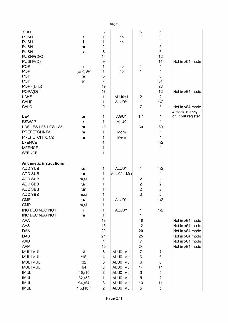
Atom
Page 271
XLAT 3 6 6PUSH r 1 np 1 1PUSH i 1 np 1PUSH m 2 5PUSH sr 3 6PUSHF(D/Q) 14 12PUSHA(D) 9 11 Not in x64 modePOP r 1 np 1 1POP (E/R)SP 1 np 1 1POP m 3 6POP sr 7 31POPF(D/Q) 19 28POPA(D) 16 12 Not in x64 modeLAHF 1 ALU0+1 2 2SAHF 1 ALU0/1 1 1/2SALC 2 7 5 Not in x64 mode
LEA r,m 1 AGU1 1-4 1BSWAP r 1 ALU0 1 1LDS LES LFS LGS LSS m 10 30 30PREFETCHNTA m 1 Mem 1PREFETCHT0/1/2 m 1 Mem 1LFENCE 1 1/2MFENCE 1 1SFENCE 1 1
Arithmetic instructionsADD SUB r,r/i 1 ALU0/1 1 1/2ADD SUB r,m 1 ALU0/1, Mem 1ADD SUB m,r/i 1 2 1ADC SBB r,r/i 1 2 2ADC SBB r,m 1 2 2ADC SBB m,r/i 1 2 2CMP r,r/i 1 ALU0/1 1 1/2CMP m,r/i 1 1INC DEC NEG NOT r 1 ALU0/1 1 1/2INC DEC NEG NOT m 1 1AAA 13 16 Not in x64 modeAAS 13 12 Not in x64 modeDAA 20 20 Not in x64 modeDAS 21 25 Not in x64 modeAAD 4 7 Not in x64 modeAAM 10 24 Not in x64 modeMUL IMUL r8 3 ALU0, Mul 7 7MUL IMUL r16 4 ALU0, Mul 6 6MUL IMUL r32 3 ALU0, Mul 6 6MUL IMUL r64 8 ALU0, Mul 14 14IMUL r16,r16 2 ALU0, Mul 6 5IMUL r32,r32 1 ALU0, Mul 5 2IMUL r64,r64 6 ALU0, Mul 13 11IMUL r16,r16,i 2 ALU0, Mul 5 5
4 clock latency on input register

Atom
Page 272
IMUL r32,r32,i 1 ALU0, Mul 5 2IMUL r64,r64,i 7 ALU0, Mul 14 14MUL IMUL m8 3 ALU0, Mul 6MUL IMUL m16 5 ALU0, Mul 7MUL IMUL m32 4 ALU0, Mul 7MUL IMUL m64 8 ALU0, Mul 14DIV r/m8 9 ALU0, Div 22 22DIV r/m16 12 ALU0, Div 33 33DIV r/m32 12 ALU0, Div 49 49DIV r/m 64 38 ALU0, Div 183 183IDIV r/m8 26 ALU0, Div 38 38IDIV r/m16 29 ALU0, Div 45 45IDIV r/m32 29 ALU0, Div 61 61IDIV r/m64 60 ALU0, Div 207 207CBW 2 ALU0 5CWDE 1 ALU0 1CDQE 1 ALU0 1CWD 2 ALU0 5CDQ 1 ALU0 1CQO 1 ALU0 1
Logic instructionsAND OR XOR r,r/i 1 ALU0/1 1 1/2AND OR XOR r,m 1 ALU0/1, Mem 1AND OR XOR m,r/i 1 ALU0/1, Me 1 1TEST r,r/i 1 ALU0/1 1 1/2TEST m,r/i 1 ALU0/1, Mem 1SHR SHL SAR r,i/cl 1 ALU0 1 1SHR SHL SAR m,i/cl 1 ALU0 1 1ROR ROL r,i/cl 1 ALU0 1 1ROR ROL m,i/cl 1 ALU0 1 1RCR r,1 5 ALU0 7RCL r,1 2 ALU0 1RCR r/m,i/cl 12-17 ALU0 12-15RCL r/m,i/cl 14-20 ALU0 14-18SHLD r16,r16,i 10 ALU0 10 1-2 more if memSHLD r32,r32,i 2 ALU0 5 1-2 more if memSHLD r64,r64,i 10 ALU0 11 1-2 more if memSHLD r16,r16,cl 9 ALU0 9 1-2 more if memSHLD r32,r32,cl 2 ALU0 5 1-2 more if memSHLD r64,r64,cl 9 ALU0 10 1-2 more if memSHRD r16,r16,i 8 ALU0 8 1-2 more if memSHRD r32,r32,i 2 ALU0 5 1-2 more if memSHRD r64,r64,i 10 ALU0 9 1-2 more if memSHRD r16,r16,cl 7 ALU0 8 1-2 more if memSHRD r32,r32,cl 2 ALU0 5 1-2 more if memSHRD r64,r64,cl 9 ALU0 9 1-2 more if memBT r,r/i 1 ALU1 1 1BT m,r 9 10BT m,i 2 5

Atom
Page 273
BTR BTS BTC r,r/i 1 ALU1 1 1BTR BTS BTC m,r 10 ALU1 11BTR BTS BTC m,i 3 ALU1 6BSF BSR r,r/m 10 16SETcc r 1 ALU0+1 2 2SETcc m 2 5CLC STC 1 ALU0/1 1/2CMC 1 2 2CLD 5 7STD 6 25
Control transfer instructionsJMP short/near 1 ALU1 2JMP far 29 66 Not in x64 modeJMP r 1 4JMP m(near) 2 7JMP m(far) 30 78Conditional jump short/near 1 ALU1 2J(E/R)CXZ short 3 7LOOP short 8 8LOOP(N)E short 8 8CALL near 1 3CALL far 37 65 Not in x64 modeCALL r 1 18CALL m(near) 2 20CALL m(far) 38 64RETN 1 np 6RETN i 1 np 6RETF 36 80RETF i 36 80BOUND r,m 11 10 Not in x64 modeINTO 4 6 Not in x64 mode
String instructionsLODS 3 6REP LODS 5n+11 3n+50STOS 2 5REP STOS 3n+10 2n+4MOVS 4 6REP MOVS 4n+11 2n - 4n fastest for high nSCAS 3 6REP SCAS 5n+16 3n+60CMPS 5 7REP CMPS 6n+16 4n+40
OtherNOP (90) 1 ALU0/1 1/2Long NOP (0F 1F) 1 ALU0/1 1/2PAUSE 5 24ENTER a,0 14 23

Atom
Page 274
ENTER a,b 20+6bLEAVE 4 6CPUID 40-80 100-170RDTSC 16 29RDPMC 24 48
Floating point x87 instructionsOperands μops Unit Latency Remarks
Move instructionsFLD r 1 1 1FLD m32/m64 1 3 1FLD m80 4 9 10FBLD m80 52 92 92FST(P) r 1 1 1FST(P) m32/m64 3 7 9FSTP m80 8 12 13FBSTP m80 189 221 221FXCH r 1 1 1FILD m 1 7 6FIST(P) m 3 11 9FISTTP m 3 11 9 SSE3FLDZ 1 1FLD1 2 8FLDPI FLDL2E etc. 2 10FCMOVcc r 3 9 9FNSTSW AX 4 10FNSTSW m16 4 10FLDCW m16 2 8FNSTCW m16 3 9FINCSTP FDECSTP 1 1 1FFREE(P) 1 1FNSAVE m 166 321 321FRSTOR m 83 177 177
Arithmetic instructionsFADD(P) FSUB(R)(P) r/m 1 5 1FMUL(P) r/m 1 Mul 5 2FDIV(R)(P) r/m 1 Div 71 71FABS 1 1 1FCHS 1 1 1FCOM(P) FUCOM r/m 1 1 1FCOMPP FUCOMPP 1 1 1FCOMI(P) FUCOMI(P) r 5 10FIADD FISUB(R) m 3 9FIMUL m 3 Mul 9FIDIV(R) m 3 Div 73FICOM(P) m 3 9FTST 1 1 1
Reciprocal throughput

Atom
Page 275
FXAM 1 1 1FPREM 26 ~110FPREM1 37 ~130FRNDINT 19 48
MathFSCALE 30 56FXTRACT 15 24FSQRT 1 Div 71FSIN FCOS 9 ~260FSINCOS 112 ~260F2XM1 25 ~100FYL2X FYL2XP1 63 ~220FPTAN 100 ~300FPATAN 91 ~300
OtherFNOP 1 1WAIT 2 5 5FNCLEX 4 26FNINIT 23 74
Integer MMX and XMM instructionsOperands μops Unit Latency Remarks
Move instructionsMOVD r32/64,(x)mm 1 4 2MOVD m32/64,(x)mm 1 Mem 5 1MOVD (x)mm,r32/64 1 3 1MOVD (x)mm,m32/64 1 Mem 4 1MOVQ (x)mm, (x)mm 1 FP0/1 1 1/2MOVQ (x)mm,m64 1 Mem 4 1MOVQ m64, (x)mm 1 Mem 5 1MOVDQA xmm, xmm 1 FP0/1 1 1/2MOVDQA xmm, m128 1 Mem 4 1MOVDQA m128, xmm 1 Mem 5 1MOVDQU m128, xmm 3 Mem 6 6MOVDQU xmm, m128 4 Mem 6 6LDDQU xmm, m128 4 Mem 6 6MOVDQ2Q mm, xmm 1 1 1MOVQ2DQ xmm,mm 1 1 1MOVNTQ m64,mm 1 Mem ~400 1MOVNTDQ m128,xmm 1 Mem ~450 3
(x)mm, (x)mm 1 FP0 1 1PUNPCKH/LBW/WD/DQ (x)mm, (x)mm 1 FP0 1 1PUNPCKH/LQDQ (x)mm, (x)mm 1 FP0 1 1
Reciprocal throughput
PACKSSWB/DW PACKUSWB
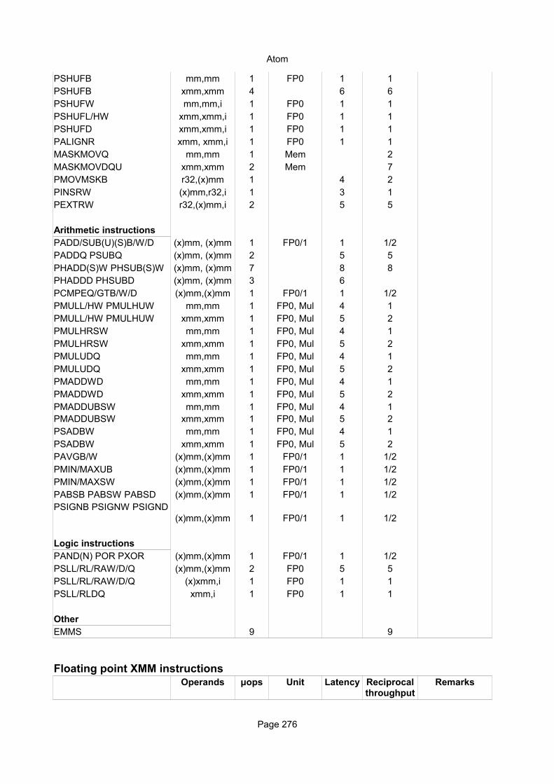
Atom
Page 276
PSHUFB mm,mm 1 FP0 1 1PSHUFB xmm,xmm 4 6 6PSHUFW mm,mm,i 1 FP0 1 1PSHUFL/HW xmm,xmm,i 1 FP0 1 1PSHUFD xmm,xmm,i 1 FP0 1 1PALIGNR xmm, xmm,i 1 FP0 1 1MASKMOVQ mm,mm 1 Mem 2MASKMOVDQU xmm,xmm 2 Mem 7PMOVMSKB r32,(x)mm 1 4 2PINSRW (x)mm,r32,i 1 3 1PEXTRW r32,(x)mm,i 2 5 5
Arithmetic instructionsPADD/SUB(U)(S)B/W/D (x)mm, (x)mm 1 FP0/1 1 1/2PADDQ PSUBQ (x)mm, (x)mm 2 5 5PHADD(S)W PHSUB(S)W (x)mm, (x)mm 7 8 8PHADDD PHSUBD (x)mm, (x)mm 3 6PCMPEQ/GTB/W/D (x)mm,(x)mm 1 FP0/1 1 1/2PMULL/HW PMULHUW mm,mm 1 FP0, Mul 4 1PMULL/HW PMULHUW xmm,xmm 1 FP0, Mul 5 2PMULHRSW mm,mm 1 FP0, Mul 4 1PMULHRSW xmm,xmm 1 FP0, Mul 5 2PMULUDQ mm,mm 1 FP0, Mul 4 1PMULUDQ xmm,xmm 1 FP0, Mul 5 2PMADDWD mm,mm 1 FP0, Mul 4 1PMADDWD xmm,xmm 1 FP0, Mul 5 2PMADDUBSW mm,mm 1 FP0, Mul 4 1PMADDUBSW xmm,xmm 1 FP0, Mul 5 2PSADBW mm,mm 1 FP0, Mul 4 1PSADBW xmm,xmm 1 FP0, Mul 5 2PAVGB/W (x)mm,(x)mm 1 FP0/1 1 1/2PMIN/MAXUB (x)mm,(x)mm 1 FP0/1 1 1/2PMIN/MAXSW (x)mm,(x)mm 1 FP0/1 1 1/2PABSB PABSW PABSD (x)mm,(x)mm 1 FP0/1 1 1/2PSIGNB PSIGNW PSIGND
(x)mm,(x)mm 1 FP0/1 1 1/2
Logic instructionsPAND(N) POR PXOR (x)mm,(x)mm 1 FP0/1 1 1/2PSLL/RL/RAW/D/Q (x)mm,(x)mm 2 FP0 5 5PSLL/RL/RAW/D/Q (x)xmm,i 1 FP0 1 1PSLL/RLDQ xmm,i 1 FP0 1 1
OtherEMMS 9 9
Floating point XMM instructionsOperands μops Unit Latency RemarksReciprocal
throughput

Atom
Page 277
Move instructionsMOVAPS/D xmm,xmm 1 FP0/1 1 1/2MOVAPS/D xmm,m128 1 Mem 4 1MOVAPS/D m128,xmm 1 Mem 5 1MOVUPS/D xmm,m128 4 Mem 6 6MOVUPS/D m128,xmm 3 Mem 6 6MOVSS/D xmm,xmm 1 FP0/1 1 1/2MOVSS/D xmm,m32/64 1 Mem 4 1MOVSS/D m32/64,xmm 1 Mem 5 1MOVHPS/D MOVLPS/D xmm,m64 1 Mem 5 1MOVHPS/D m64,xmm 1 Mem 4 1MOVLPS/D m64,xmm 1 Mem 4 1MOVLHPS MOVHLPS xmm,xmm 1 FP0 1 1MOVMSKPS/D r32,xmm 1 4 2MOVNTPS/D m128,xmm 1 Mem ~500 3SHUFPS xmm,xmm,i 1 FP0 1 1SHUFPD xmm,xmm,i 1 FP0 1 1MOVDDUP xmm,xmm 1 FP0 1 1MOVSH/LDUP xmm,xmm 1 FP0 1 1UNPCKH/LPS xmm,xmm 1 FP0 1 1UNPCKH/LPD xmm,xmm 1 FP0 1
ConversionCVTPD2PS xmm,xmm 4 11 11CVTSD2SS xmm,xmm 3 10 10CVTPS2PD xmm,xmm 4 7 6CVTSS2SD xmm,xmm 3 6 6CVTDQ2PS xmm,xmm 3 6 6CVT(T) PS2DQ xmm,xmm 3 6 6CVTDQ2PD xmm,xmm 3 7 6CVT(T)PD2DQ xmm,xmm 3 6 6CVTPI2PS xmm,mm 1 6 5CVT(T)PS2PI mm,xmm 1 4 1CVTPI2PD xmm,mm 3 7 6CVT(T) PD2PI mm,xmm 4 7 7CVTSI2SS xmm,r32 3 7 6CVT(T)SS2SI r32,xmm 3 10 8CVTSI2SD xmm,r32 3 8 6CVT(T)SD2SI r32,xmm 3 10 8
ArithmeticADDSS SUBSS xmm,xmm 1 FP1 5 1ADDSD SUBSD xmm,xmm 1 FP1 5 1ADDPS SUBPS xmm,xmm 1 FP1 5 1ADDPD SUBPD xmm,xmm 3 FP1 6 6ADDSUBPS xmm,xmm 1 FP1 5 1ADDSUBPD xmm,xmm 3 FP1 6 6HADDPS HSUBPS xmm,xmm 5 FP0+1 8 7HADDPD HSUBPD xmm,xmm 5 FP0+1 8 7MULSS xmm,xmm 1 FP0, Mul 4 1

Atom
Page 278
MULSD xmm,xmm 1 FP0, Mul 5 2MULPS xmm,xmm 1 FP0, Mul 5 2MULPD xmm,xmm 6 FP0, Mul 9 9DIVSS xmm,xmm 3 FP0, Div 31 31DIVSD xmm,xmm 3 FP0, Div 60 60DIVPS xmm,xmm 6 FP0, Div 64 64DIVPD xmm,xmm 6 FP0, Div 122 122RCPSS xmm,xmm 1 4 1RCPPS xmm,xmm 5 9 8CMPccSS/D xmm,xmm 1 FP0 5 1CMPccPS/D xmm,xmm 3 FP0 6 6COMISS/D UCOMISS/D xmm,xmm 4 FP0 9 9MAXSS/D MINSS/D xmm,xmm 1 FP0 5 1MAXPS/D MINPS/D xmm,xmm 3 FP0 6 6
MathSQRTSS xmm,xmm 3 FP0, Div 31 31SQRTPS xmm,xmm 5 FP0, Div 63 63SQRTSD xmm,xmm 3 FP0, Div 60 60SQRTPD xmm,xmm 5 FP0, Div 121 121RSQRTSS xmm,xmm 1 FP0 4 1RSQRTPS xmm,xmm 5 FP0 9 8
LogicANDPS/D xmm,xmm 1 FP0/1 1 1/2ANDNPS/D xmm,xmm 1 FP0/1 1 1/2ORPS/D xmm,xmm 1 FP0/1 1 1/2XORPS/D xmm,xmm 1 FP0/1 1 1/2
OtherLDMXCSR m32 4 5 6STMXCSR m32 4 14 15FXSAVE m4096 121 142 144FXRSTOR m4096 116 149 150
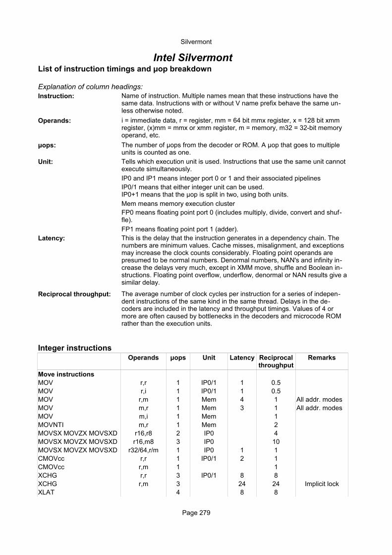
Silvermont
Page 279
Intel SilvermontList of instruction timings and μop breakdown
Explanation of column headings:Instruction:
Operands:
μops:
Unit:
IP0 and IP1 means integer port 0 or 1 and their associated pipelines
Mem means memory execution cluster
FP1 means floating point port 1 (adder).Latency:
Reciprocal throughput:
Integer instructionsOperands μops Unit Latency Remarks
Move instructionsMOV r,r 1 IP0/1 1 0.5MOV r,i 1 IP0/1 1 0.5MOV r,m 1 Mem 4 1 All addr. modesMOV m,r 1 Mem 3 1 All addr. modesMOV m,i 1 Mem 1MOVNTI m,r 1 Mem 2MOVSX MOVZX MOVSXD r16,r8 2 IP0 4MOVSX MOVZX MOVSXD r16,m8 3 IP0 10MOVSX MOVZX MOVSXD r32/64,r/m 1 IP0 1 1CMOVcc r,r 1 IP0/1 2 1CMOVcc r,m 1 1XCHG r,r 3 IP0/1 8 8XCHG r,m 3 24 24 Implicit lockXLAT 4 8 8
Name of instruction. Multiple names mean that these instructions have the same data. Instructions with or without V name prefix behave the same un-less otherwise noted.
i = immediate data, r = register, mm = 64 bit mmx register, x = 128 bit xmm register, (x)mm = mmx or xmm register, m = memory, m32 = 32-bit memory operand, etc.
The number of μops from the decoder or ROM. A µop that goes to multiple units is counted as one.Tells which execution unit is used. Instructions that use the same unit cannot execute simultaneously.
IP0/1 means that either integer unit can be used.IP0+1 means that the µop is split in two, using both units.
FP0 means floating point port 0 (includes multiply, divide, convert and shuf-fle).
This is the delay that the instruction generates in a dependency chain. The numbers are minimum values. Cache misses, misalignment, and exceptions may increase the clock counts considerably. Floating point operands are presumed to be normal numbers. Denormal numbers, NAN's and infinity in-crease the delays very much, except in XMM move, shuffle and Boolean in-structions. Floating point overflow, underflow, denormal or NAN results give a similar delay.
The average number of clock cycles per instruction for a series of indepen-dent instructions of the same kind in the same thread. Delays in the de-coders are included in the latency and throughput timings. Values of 4 or more are often caused by bottlenecks in the decoders and microcode ROM rather than the execution units.
Reciprocal throughput

Silvermont
Page 280
PUSH r 1 IP0+1 1PUSH i 1 IP0+1 1PUSH m 3 IP0+1 5PUSHF(D/Q) 18 IP0+1 29PUSHA(D) 10 10 Not in x64 modePOP r 2 1POP (E/R)SP 2 3POP m 6 6POPF(D/Q) 21 47POPA(D) 17 14 Not in x64 modeLAHF 1 1 1SAHF 1 IP0 2 1SALC 2 6 4 Not in x64 modeLEA r,[r+d] 1 IP0/1 1 1LEA r,[r+r*s] 1 IP1 1 1LEA r,[r+r*s+d] 1 IP0+1 2 2LEA r,[rip+d] 1 IP0/1 0.5LEA r16,[m] 2 4 4BSWAP r 1 IP0 1 1MOVBE r16,m16 1 2MOVBE r32/64,m32/64 1 1MOVBE m,r 1 1PREFETCHNTA m 1 1PREFETCHT0/1/2 m 1 1PREFETCHNTW m 1 1LFENCE 2 8MFENCE 2 14SFENCE 1 7
Arithmetic instructionsADD SUB r,r/i 1 IP0/1 1 0.5ADD SUB r,m 1 IP0/1, Mem 1ADD SUB m,r/i 1 IP0/1, Mem 6 1ADC SBB r,r/i 1 IP0/1 2 2ADC SBB r,m 1 2ADC SBB m,r/i 1 6 2ADCX r32,r32 1 IP0+1 2 2ADCX r64,r64 1 IP0+1 6 6ADOX r32,r32 1 2 2ADOX r64,r64 1 6 6CMP r,r/i 1 IP0/1 1 0.5CMP m,r/i 1 1INC DEC r 1 IP0/1 1 0.5 latency to flag=2NEG NOT r 1 IP0/1 1 0.5INC DEC NEG NOT m 1 6 1AAA 13 12 Not in x64 modeAAS 13 12 Not in x64 modeDAA 20 16 Not in x64 modeDAS 21 16 Not in x64 modeAAD 4 5 Not in x64 modeAAM 11 24 16 Not in x64 modeMUL IMUL r8 3 IP0 5 5MUL IMUL r16 4 IP0 5 5

Silvermont
Page 281
MUL IMUL r32 3 IP0 5 5MUL IMUL r64 3 IP0 7 7IMUL r16,r16 2 IP0 4 4IMUL r32,r32 1 IP0 3 1IMUL r64,r64 1 IP0 5 2IMUL r16,r16,i 2 IP0 4 4IMUL r32,r32,i 1 IP0 3 1IMUL r64,r64,i 1 IP0 5 2MUL IMUL m8 3 IP0MUL IMUL m16 5 IP0MUL IMUL m32 4 IP0MUL IMUL m64 4 IP0 14MULX r,r,r 3-4 IP0 8 8MULX r,r,m 4 IP0 8-10DIV r/m8 9 IP0, FP0 24 19DIV r/m16 12 IP0, FP0 25-29 19-23DIV r/m32 12 IP0, FP0 25-39 19-31DIV r/m 64 23 IP0, FP0 34-94 25-94IDIV r/m8 26 IP0, FP0 24-35 25IDIV r/m16 29 IP0, FP0 37-41 30-32IDIV r/m32 29 IP0, FP0 29-46 29-38IDIV r/m64 44 IP0, FP0 47-107 47-107CBW 2 IP0 4CWDE 1 IP0 1CDQE 1 IP0 1CWD 2 IP0 4CDQ 1 IP0 1CQO 1 IP0 1POPCNT r16,r16 2 4 4POPCNT r32,r32 1 3 1POPCNT r64,r64 1 3 1CRC32 r32,r8 2 4 4CRC32 r32,r16 1 6 6CRC32 r32,r32 1 3 1
Logic instructionsAND OR XOR r,r/i 1 IP0/1 1 0.5AND OR XOR r,m 1 IP0/1, Mem 1AND OR XOR m,r/i 1 IP0/1, Mem 6 1TEST r,r/i 1 IP0/1 1 0.5TEST m,r/i 1 IP0/1, Mem 1SHR SHL SAR r,i/cl 1 IP0 1 1SHR SHL SAR m,i/cl 1 IP0 1 1ROR ROL r,i/cl 1 IP0 1 1ROR ROL m,i/cl 1 IP0 1RCR r,1 7 IP0 9RCL r,1 1 IP0 2 2RCR r,i/cl 11 IP0 12RCR m,i/cl 14 IP0 13RCL r,i/cl 13 IP0 12RCL m,i/cl 16 IP0 14SHLD r16,r16,i 10 IP0 10 2 more if memSHLD r32,r32,i 1 IP0 2 4 more if mem

Silvermont
Page 282
SHLD r64,r64,i 10 IP0 10 2 more if memSHLD r16,r16,cl 9 IP0 10 2 more if memSHLD r32,r32,cl 2 IP0 4 2 more if memSHLD r64,r64,cl 9 IP0 10 2 more if memSHRD r16,r16,i 8 IP0 10 3 more if memSHRD r32,r32,i 2 IP0 4 4 more if memSHRD r64,r64,i 8-10 IP0 10 3 more if memSHRD r16,r16,cl 7 IP0 10 2 more if memSHRD r32,r32,cl 2 IP0 4 2 more if memSHRD r64,r64,cl 2 IP0 4 2 more if memBT r,r/i 1 IP0+1 1 1BT m,r 7 9BT m,i 1 1BTR BTS BTC r,r/i 1 IP0+1 1 1BTR BTS BTC m,r 8 10BTR BTS BTC m,i 1 IP0+1 1BSF BSR r,r/m 10 IP0+1 10 10SETcc r/m 1 IP0+1 2 1CLC STC 1 IP0/1 1CMC 1 1 1CLD 4 IP0+1 7STD 5 IP0+1 35
Control transfer instructionsJMP short/near 1 IP1 2JMP r 1 2JMP m(near) 1 2Conditional jump short/near 1 IP1 1-2J(E/R)CXZ short 2 2-15LOOP short 7 10-20LOOP(N)E short 8CALL near 1 2CALL r 1 9CALL m 3 14RET 1 3RET i 1 3BOUND r,m 10 10 Not in x64 modeINTO 4 7 Not in x64 mode
String instructionsLODS 3 5REP LODS ~4n ~2nSTOS 2 4
REP STOS ~0.12B ~0.1BMOVS 5 6
REP MOVS ~ 0.2B ~0.15BSCAS 3 5REP SCAS ~5n ~3nCMPS 6 6REP CMPS ~6n ~3n
per byte, best case
per byte, best case
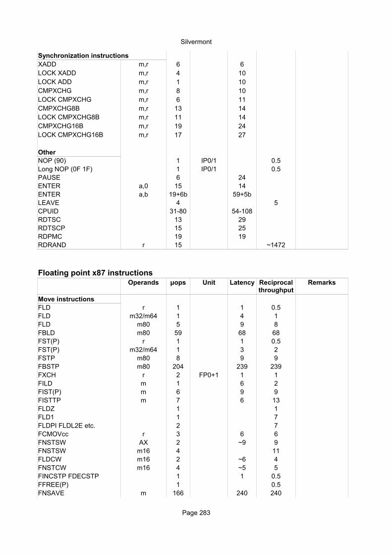
Silvermont
Page 283
Synchronization instructionsXADD m,r 6 6LOCK XADD m,r 4 10LOCK ADD m,r 1 10CMPXCHG m,r 8 10LOCK CMPXCHG m,r 6 11CMPXCHG8B m,r 13 14LOCK CMPXCHG8B m,r 11 14CMPXCHG16B m,r 19 24LOCK CMPXCHG16B m,r 17 27
OtherNOP (90) 1 IP0/1 0.5Long NOP (0F 1F) 1 IP0/1 0.5PAUSE 6 24ENTER a,0 15 14ENTER a,b 19+6b 59+5bLEAVE 4 5CPUID 31-80 54-108RDTSC 13 29RDTSCP 15 25RDPMC 19 19RDRAND r 15 ~1472
Floating point x87 instructionsOperands μops Unit Latency Remarks
Move instructionsFLD r 1 1 0.5FLD m32/m64 1 4 1FLD m80 5 9 8FBLD m80 59 68 68FST(P) r 1 1 0.5FST(P) m32/m64 1 3 2FSTP m80 8 9 9FBSTP m80 204 239 239FXCH r 2 FP0+1 1 1FILD m 1 6 2FIST(P) m 6 9 9FISTTP m 7 6 13FLDZ 1 1FLD1 1 7FLDPI FLDL2E etc. 2 7FCMOVcc r 3 6 6FNSTSW AX 2 ~9 9FNSTSW m16 4 11FLDCW m16 2 ~6 4FNSTCW m16 4 ~5 5FINCSTP FDECSTP 1 1 0.5FFREE(P) 1 0.5FNSAVE m 166 240 240
Reciprocal throughput

Silvermont
Page 284
FRSTOR m 82 174 174
Arithmetic instructionsFADD(P) FSUB(R)(P) r/m 1 FP1 3 1FMUL(P) r/m 1 FP0 5 2FDIV(R)(P) r/m 1 FP0 39 37FABS 1 1 1FCHS 1 1 1FCOM(P) FUCOM r/m 1 5 1FCOMPP FUCOMPP 1 5 1FCOMI(P) FUCOMI(P) r 1 5 1FIADD FISUB(R) m 3 5FIMUL m 3 6FIDIV(R) m 3 39FICOM(P) m 3 5FTST 1 6 1FXAM 1 7 1FPREM 27 32-57 32-57FPREM1 27 32-57 32-57FRNDINT 18 26 26
MathFSCALE 27 66FXTRACT 15 20 20FSQRT 1 13-40 13-40FSIN FCOS 18 40-170 40-170FSINCOS 110 40-170F2XM1 9 39-90FYL2X 34 80-140FYL2XP1 61 154FPTAN 101 45-200FPATAN 63 85-190
OtherFNOP 1 0.5WAIT 2 4FNCLEX 4 24FNINIT 19 65
Integer MMX and XMM instructionsOperands μops Unit Latency Remarks
Move instructionsMOVD MOVQ r32/64,(x)mm 1 4 1MOVD MOVQ m,(x)mm 1 Mem 3 1MOVD MOVQ (x)mm,r32/64 1 3 1MOVD MOVQ (x)mm,m 1 Mem 4 1MOVQ (x)mm, (x)mm 1 FP0/1 1 0.5MOVDQA x, x 1 FP0/1 1 0.5MOVDQA MOVDQU x, m128 1 Mem 4 1
Reciprocal throughput

Silvermont
Page 285
MOVDQA MOVDQU m128, x 1 Mem 3 1LDDQU x, m128 1 Mem 4 1MOVDQ2Q mm, x 1 1 1MOVQ2DQ x,mm 1 1 1MOVNTQ m64,mm 1 Mem ~370 1MOVNTDQ m128,x 1 Mem ~370 1MOVNTDQA x, m128 1 4 1
(x)mm, (x)mm 1 FP0 1 1PACKUSDW x,x 1 FP0 1 1PUNPCKH/LBW/WD/DQ (x)mm, (x)mm 1 FP0 1 1PUNPCKH/LQDQ (x)mm, (x)mm 1 FP0 1 1
x,x 1 1 1
x,m 1 1 1PSHUFB mm,mm 1 FP0 1 1PSHUFB x,x 4 FP0 5 5PSHUFW mm,mm,i 1 FP0 1 1PSHUFL/HW x,x,i 1 FP0 1 1PSHUFD x,x,i 1 FP0 1 1PALIGNR x,x,i 1 FP0 1 1PBLENDVB x,x,xmm0 2 FP0 4 4PBLENDVB x,m,xmm0 3 FP0 5PBLENDW x,x/m,i 1 FP0 1 1MASKMOVQ mm,mm 1 Mem ~370 1MASKMOVDQU x,x 3 Mem ~370 5PMOVMSKB r32,(x)mm 1 4 1PINSRW (x)mm,r32,i 1 3 1PINSRB/D/Q x,r32,i 1 3 1PINSRB/D/Q x,m8,i 1 1PEXTRW r32,(x)mm,i 2 5 4PEXTRB/W r32,x,i 2 5 4PEXTRQ r64,x,i 2 7 7PEXTRB/W m8/16,x,i 5 6PEXTRD m32,x,i 4 5PEXTRQ m64,x,i 4 8
Arithmetic instructionsPADD/SUB(U)(S)B/W/D (x)mm, (x)mm 1 FP0/1 1 0.5PADDQ PSUBQ (x)mm, (x)mm 2 4 4PADDQ PSUBQ (x)mm, m 3 5PHADD(S)W PHSUB(S)W mm, mm 5 6 6PHADD(S)W PHSUB(S)W x, x/m 7-8 9 9PHADDD PHSUBD (x)mm, (x)mm 3-4 5-6 5-6PCMPEQ/GTB/W/D (x)mm,(x)mm 1 FP0/1 1 0.5PCMPEQQ x, x 2 4 4 +1 if memPCMPGTQ x, x 1 FP0 5 2PMULL/HW PMULHUW mm,mm 1 FP0 4 1PMULL/HW PMULHUW x, x 1 FP0 5 2PMULHRSW mm,mm 1 FP0 4 1PMULHRSW x, x 1 FP0 5 2PMULLD x, x 7 FP0 11 11 +1 if mem
PACKSSWB/DW PACKUSWB
PMOVSX/ZX BW BD BQ DW DQ
PMOVSX/ZX BW BD BQ DW DQ

Silvermont
Page 286
PMULDQ x, x 1 FP0 5 2PMULUDQ mm,mm 1 FP0 4 1PMULUDQ x, x 1 FP0 5 2PMADDWD mm,mm 1 FP0 4 1PMADDWD x, x 1 FP0 5 2PMADDUBSW mm,mm 1 FP0 4 1PMADDUBSW x, x 1 FP0 5 2PSADBW mm,mm 1 FP0 4 1PSADBW x, x 1 FP0 5 2MPSADBW x,x,i 3 7 6MPSADBW x,m,i 4 6PAVGB/W (x)mm,(x)mm 1 FP0/1 1 0.5PMIN/MAXUB (x)mm,(x)mm 1 FP0/1 1 0.5PMIN/MAXSW (x)mm,(x)mm 1 FP0/1 1 0.5
x,x 1 1 1PHMINPOSUW x,x 1 FP0 5 2PABSB PABSW PABSD (x)mm,(x)mm 1 FP0/1 1 0.5-1PSIGNB PSIGNW PSIGND
(x)mm,(x)mm 1 FP0/1 1 0.5-1
Logic instructionsPAND(N) POR PXOR (x)mm,(x)mm 1 FP0/1 1 0.5PTEST x,x 1 1 1PSLL/RL/RAW/D/Q (x)mm,(x)mm 2 FP0 2 2PSLL/RL/RAW/D/Q (x)mm,i 1 FP0 1 1PSLL/RLDQ x,i 1 FP0 1 1
String instructionsPCMPESTRI x,x,i 9 FP0 21 21 +1 if memPCMPESTRM x,x,i 8 FP0 17 17 +1 if memPCMPISTRI x,x,i 6 FP0 17 17 +1 if memPCMPISTRM x,x,i 5 FP0 13 13 +1 if mem
Encryption instructionsPCLMULQDQ x,x,i 8 FP0 10 10 +1 if mem
OtherEMMS 9 10
Floating point XMM instructionsOperands μops Unit Latency Remarks
Move instructionsMOVAPS/D x, x 1 FP0/1 1 0.5MOVAPS/D x,m128 1 Mem 4 1MOVAPS/D m128,x 1 Mem 3 1MOVUPS/D x,m128 1 Mem 4 1MOVUPS/D m128,x 1 Mem 3 1MOVSS/D x, x 1 FP0/1 1 0.5MOVSS/D x,m32/64 1 Mem 4 1
PMIN/PMAXSB/SW/SDUB/UW/UD
Reciprocal throughput

Silvermont
Page 287
MOVSS/D m32/64,x 1 Mem 3 1MOVHPS/D MOVLPS/D x,m64 1 Mem 4 1MOVHPS/D MOVLPS/D m64,x 1 Mem 3 1MOVLHPS MOVHLPS x,x 1 FP0 1 1BLENDPS/PD x,x/m,i 1 1 1BLENDVPS/PD x,x,xmm0 2 FP0+1 4 4BLENDVPS/PD x,m,xmm0 3 FP0+1 5 5INSERTPS x,x,i 1 1 1INSERTPS x,m32,i 3 5 5EXTRACTPS r32,x,i 2 4EXTRACTPS m32,x,i 4 4 5MOVMSKPS/D r32,x 1 FP0 4 1MOVNTPS/D m128,x 1 Mem ~370 1SHUFPS x,x,i 1 FP0 1 1SHUFPD x,x,i 1 FP0 1 1MOVDDUP x, x 1 FP0 1 1MOVSH/LDUP x, x 1 FP0 1 1UNPCKH/LPS x, x 1 FP0 1 1UNPCKH/LPD x, x 1 FP0 1 1
ConversionCVTPD2PS x, x 1 FP0 5 2CVTSD2SS x, x 1 FP0 4 2CVTPS2PD x, x 1 FP0 5 2CVTSS2SD x, x 1 FP0 4 2CVTDQ2PS x, x 1 FP0 5 2CVT(T) PS2DQ x, x 1 FP0 5 2CVTDQ2PD x, x 1 FP0 5 2CVT(T)PD2DQ x, x 1 FP0 5 2CVTPI2PS x,mm 1 FP0 4 2CVT(T)PS2PI mm,x 1 FP0 4 2CVTPI2PD x,mm 1 FP0 5 2CVT(T) PD2PI mm,x 1 FP0 5 2CVTSI2SS x,r32 1 FP0 5 2CVT(T)SS2SI r32,x 1 FP0 5 1CVTSI2SD xm,r32 1 FP0 5 2CVT(T)SD2SI r32,x 3 FP0 5 1
ArithmeticADDSS SUBSS x, x 1 FP1 3 1ADDSD SUBSD x, x 1 FP1 3 1ADDPS SUBPS x, x 1 FP1 3 1ADDPD SUBPD x, x 1 FP1 4 2ADDSUBPS x, x 1 FP1 3 1ADDSUBPD x, x 1 FP1 4 2HADDPS HSUBPS x, x 4 6 6 +1 if memHADDPD HSUBPD x, x 4 6 5 +1 if memMULSS x, x 1 FP0 4 1MULSD x, x 1 FP0 5 2MULPS x, x 1 FP0 5 2MULPD x, x 1 FP0 7 4DIVSS x, x 1 FP0 19 17DIVSD x, x 1 FP0 34 32

Silvermont
Page 288
DIVPS x, x 6 FP0 39 39DIVPD x, x 6 FP0 69 69RCPSS x, x 1 FP0 4 1RCPPS x, x 5 FP0 9 8CMPccSS/D PS/D x, x 1 FP1 3 1COMISS/D UCOMISS/D x, x 1 FP1 1MAXSS/D MINSS/D x, x 1 FP1 3 1MAXPS MINPS x, x 1 FP1 3 1MAXPD MINPD x, x 1 FP1 4 2ROUNDSS/D x,x,i 1 FP0 4 2ROUNDPS/D x,x,i 1 FP0 5 2DPPS x,x,i 9 FP0 15 12 +1 if memDPPD x,x,i 5 FP0 12 8 +1 if mem
MathSQRTSS x, x 1 FP0 20 18SQRTPS x, x 5 FP0 40 40SQRTSD x, x 1 FP0 35 33SQRTPD x, x 5 FP0 70 70RSQRTSS x, x 1 FP0 4 1RSQRTPS x, x 5 FP0 9 8
LogicANDPS/D x, x 1 FP0/1 1 0.5ANDNPS/D x, x 1 FP0/1 1 0.5ORPS/D x, x 1 FP0/1 1 0.5XORPS/D x, x 1 FP0/1 1 0.5
OtherLDMXCSR m32 5 10 8STMXCSR m32 4 12 11FXSAVE m4096 115 132 132 32 bit modeFXSAVE m4096 123 143 143 64 bit modeFXRSTOR m4096 114 118 118 32 bit modeFXRSTOR m4096 123 122 122 64 bit mode

Knights Landing
Page 289
Intel Knights LandingList of instruction timings and μop breakdown
Explanation of column headings:Instruction:
Operands:
μops:
Unit:
IP0 and IP1 means integer port 0 or 1 and their associated pipelines
Mem means memory execution clusterFP0 means floating point port 0 (includes multiply, divide, convert and shuffle).
FP1 means floating point port 1.Latency:
Reciprocal throughput:
Integer instructionsOperands μops Unit Latency Remarks
Move instructionsMOV r,r 1 IP0/1 1 0.5MOV r,i 1 IP0/1 1 0.5MOV r,m 1 Mem 4 1 All addr. modesMOV m,r 1 Mem 3 1 All addr. modesMOV m,i 1 Mem 1MOVNTI m,r 1 Mem 2
Name of instruction. Multiple names mean that these instructions have the same data. Instructions with or without V name prefix behave the same unless otherwise noted.
i = immediate data, r = register, mm = 64 bit mmx register, x = 128 bit xmm register, (x)mm = mmx or xmm register, y = 256 bit ymm register, z = 512 bit zmm register, v = any vector register (mmx, xmm, ymm, zmm), k = mask regis-ter. same = same register for both operands. m = memory operand, m32 = 32-bit memory operand, etc.
The number of μops from the decoder or ROM. A µop that goes to multiple units is counted as one.Tells which execution unit is used. Instructions that use the same unit cannot execute simultaneously.
IP0/1 means that either integer unit can be used.IP0+1 means that the µop is split in two, using both units.
This is the delay that the instruction generates in a dependency chain. The numbers are minimum values. Cache misses, misalignment, and exceptions may increase the clock counts considerably. Floating point operands are pre-sumed to be normal numbers. Denormal numbers, NAN's and infinity increase the delays very much, except in XMM move, shuffle and Boolean instructions. Floating point overflow, underflow, denormal or NAN results give a similar de-lay.
Some instructions have a range of latencies. For example VPSHUFD has a la-tency of 3-6. The short latency is measured in a chain of similar instructions. The long latency is measured when the input comes from an instruction of a different type and the output goes to an instruction of a different type, for ex-ample a move instruction. The long latency will apply in most cases. Division and some square root instructions have latencies that depend on the values of the operands.
The average number of clock cycles per instruction for a series of independent instructions of the same kind in the same thread. Delays in the decoders are included in the latency and throughput timings. Values of 4 or more are often caused by bottlenecks in the decoders and microcode ROM rather than the execution units.
Reciprocal throughput

Knights Landing
Page 290
MOVSX MOVZX MOVSXD r16,r8 2 IP0 7 7MOVSX MOVZX MOVSXD r16,m8 3 IP0 7 8MOVSX MOVZX MOVSXD r32/64,r 1 IP0 1 1MOVSX MOVZX MOVSXD r32/64,m 1 IP0 4 1CMOVcc r,r 1 IP0/1 2 1CMOVcc r,m 1 1XCHG r,r 3 IP0/1 8 8XCHG r,m 3 24 24 Implicit lockXLAT 4 8PUSH r 1 1PUSH i 1 IP0+1 1PUSH m 3 IP0+1 8PUSHF(D/Q) 18 IP0+1 28PUSHA(D) 10 10 Not in x64 modePOP r 2 1POP (E/R)SP 2 4POP m 6 9POPF(D/Q) 21 48POPA(D) 17 15 Not in x64 modeLAHF 1 IP0 1 1SAHF 1 IP0 2 1SALC 2 9 7 Not in x64 modeLEA r,[r+d] 1 IP0/1 1 0.5LEA r,[r+r*s] 1 IP1 1 1LEA r,[r+r*s+d] 1 IP0+1 2 1LEA r,[rip+d] 1 IP0/1 0.5LEA r16,[m] 2 7BSWAP r 1 IP0 1 1MOVBE r16,m16 1 1MOVBE r/m32/64 1 1MOVBE m,r 1 1PREFETCHNTA m 1 0.5PREFETCHT0/1/2 m 1 0.5PREFETCHNTW m 1 0.5LFENCE 2 8MFENCE 2 17SFENCE 1 10
Arithmetic instructionsADD SUB r,r/i 1 IP0/1 1 0.5ADD SUB r,m 1 IP0/1, Mem 1ADD SUB m,r/i 1 IP0/1, Mem 7 1ADC SBB r,r/i 1 IP0+1 2 2ADC SBB r,m 1 2ADC SBB m,r/i 1 7 2ADCX ADOX r32,r32 1 IP0+1 2 2ADCX ADOX r64,r64 1 IP0+1 2 6 due to decoderCMP r,r/i 1 IP0/1 1 0.5CMP m,r/i 1 1INC DEC r 1 IP0/1 1-2 0.5NEG NOT r 1 IP0/1 1 0.5INC DEC NEG NOT m 1 7 1AAA AAS 13 13 Not in x64 mode

Knights Landing
Page 291
DAA 20 17 Not in x64 modeDAS 21 17 Not in x64 modeAAD 4 8 Not in x64 modeAAM 10 30 14 Not in x64 modeMUL IMUL r8 3 IP0 8MUL IMUL r16 4 IP0 8MUL IMUL r32 3 IP0 8MUL IMUL r64 3 IP0 8IMUL r16,r16 2 IP0 7 7IMUL r32,r32 1 IP0 3 1IMUL r64,r64 1 IP0 5 2IMUL r16,r16,i 2 IP0 7 7IMUL r32,r32,i 1 IP0 3 1IMUL r64,r64,i 1 IP0 5 2MUL IMUL m8 3 IP0MUL IMUL m16 3 IP0MUL IMUL m32 4 IP0MUL IMUL m64 3 IP0DIV r/m8 9 IP0, FP0 30 12DIV r/m16 12 IP0, FP0 30-35 13-15DIV r/m32 12 IP0, FP0 29-42 13-23DIV r/m 64 23 IP0, FP0 39-95 22-95IDIV r/m8 26 IP0, FP0 39 20IDIV r/m16 29 IP0, FP0 38-42 22IDIV r/m32 29 IP0, FP0 37-49 22-26IDIV r/m64 44 IP0, FP0 53-108 36-107CBW 2 IP0 7CWDE 1 IP0 1CDQE 1 IP0 1CWD 2 IP0 7CDQ 1 IP0 1CQO 1 IP0 1POPCNT r16,r16 2 7 7POPCNT r32,r32 1 3 1POPCNT r64,r64 1 3 1CRC32 r32,r8 2 7 2CRC32 r32,r16 1 6 6CRC32 r32,r32 1 3 1CRC32 r64,r64 1 6 1
Logic instructionsAND OR XOR r,r/i 1 IP0/1 1 0.5AND OR XOR r,m 1 IP0/1, Mem 1AND OR XOR m,r/i 1 IP0/1, Mem 6 1TEST r,r/i 1 IP0/1 1 0.5TEST m,r/i 1 IP0/1, Mem 1SHR SHL SAR r,i/cl 1 IP0 1 1SHR SHL SAR m,i/cl 1 IP0 1ROR ROL r,i/cl 1 IP0 1 1ROR ROL m,i/cl 1 IP0 1RCR r,1 7 IP0 10 10RCL r,1 1 IP0 2 2RCR r,i/cl 11 IP0 13 13

Knights Landing
Page 292
RCR m,i/cl 14 IP0 13RCL r,i/cl 13 IP0 13 13RCL m,i/cl 16 IP0 16 16SHLD r16,r16,i 10 IP0 11 11SHLD r16,m16,i 13 IP0 13 13SHLD r32,r32,i 1 IP0 2 2SHLD r32,m32,i 6 IP0 9 9SHLD r64,r64,i 10 IP0 11 11SHLD r64,m64,i 13 IP0 13 13SHLD r16,r16,cl 9 IP0 11 11SHLD r16,m16,cl 12 IP0 13 13SHLD r32,r32,cl 2 IP0 7 7SHLD r32,m32,cl 6 IP0 9 9SHLD r64,r64,cl 9 IP0 11 11SHLD r64,m64,cl 12 IP0 13 13SHRD r16,r16,i 8 IP0 11 11SHRD r16,m16,i 11 IP0 12 12SHRD r32,r32,i 2 IP0 7 7SHRD r32,m32,i 6 IP0 9 9SHRD r64,r64,i 10 IP0 11 11SHRD r64,m64,i 13 IP0 15 15SHRD r16,r16,cl 7 IP0 11 11SHRD r16,m16,cl 10 IP0 12 12SHRD r32,r32,cl 2 IP0 7 7SHRD r32,r32,cl 6 IP0 9 9SHRD r64,r64,cl 9 IP0 11 11SHRD r64,m64,cl 12 IP0 14 14SHLX SHRX SARX r,r,r 1 IP0 2 1RORX r,r,i 1 IP0 1 1BT r,r/i 1 IP0+1 1 1BT m,r 7 10 10BT m,i 1 1 1BTR BTS BTC r,r/i 1 IP0+1 1 1BTR BTS BTC m,r 8 11 11BTR BTS BTC m,i 1 IP0+1 1 1BSF BSR r,r/m 10 IP0/1 11 11SETcc r/m 1 IP0+1 2 1CLC STC 1 IP0 1CMC 1 IP0 1 1CLD 4 IP0/1 8STD 5 IP0/1 36LZCNT r,r/m 1 3 1TZCNT r,r/m 1 3 1ANDN r,r,r 1 1 0.5ANDN r,r,m 1 1 1BLSI BLSMSK BLSR r,r/m 1 1 1BEXTR r,r,r 2 7 7BEXTR r,r,m 3 8BZHI r,r,r 1 3 1PDEP r,r,r 1 3 1PEXT r,r,r 1 3 1
Control transfer instructions

Knights Landing
Page 293
JMP short/near 1 IP1 2JMP r 1 IP1 2JMP m(near) 1 IP1 2Conditional jump short/near 1 IP1 1-2J(E/R)CXZ short 2 7-18LOOP short 7 14-23LOOP(N)E short 8 14-23CALL near 1 2CALL r 1 2CALL m 3 14RET 1 2RET i 1 2BOUND r,m 10 11 Not in x64 modeINTO 4 8 Not in x64 mode
String instructionsLODS 3 8REP LODS ~4n ~2nSTOS 2 7REP STOS ~0.07B ~0.054B per byte, best case
MOVS 5 9REP MOVS ~ 0.1B ~0.08B per byte, best case
SCAS 3 8REP SCAS ~5n ~3nCMPS 6 9REP CMPS ~6n ~3n
Synchronization instructionsXADD m,r 6 9LOCK XADD m,r 4 24LOCK ADD m,r 1 13CMPXCHG m,r 8 11LOCK CMPXCHG m,r 6 26CMPXCHG8B m,r 13 15LOCK CMPXCHG8B m,r 11 29CMPXCHG16B m,r 19 31LOCK CMPXCHG16B m,r 17 48
OtherNOP (90) 1 IP0/1 0.5Long NOP (0F 1F) 1 IP0/1 0.5PAUSE 6 25ENTER a,0 15 14ENTER a,b 19+6b 66+4bLEAVE 4 8 5XGETBV 7 14CPUID 40-83 63-270RDTSC 15 30RDTSCP 17 36RDPMC 19 20RDRAND r 17 200RDSEED r 17 200

Knights Landing
Page 294
Floating point x87 instructionsOperands μops Unit Latency Remarks
Move instructionsFLD r 1 2 1FLD m32/m64 1 8 1FLD m80 5 9 12FBLD m80 52 66FST(P) r 1 2 1FST m32/m64 5 14 13FSTP m32/m64 6 14 13FSTP m80 8 11 14FBSTP m80 189 264FXCH r 3 FP0+1 9 9FILD m 1 5 2FIST(P) m 6 18 12FISTTP m 6 14FLDZ 1 1FLD1 2 10FLDPI FLDL2E etc. 2 10FCMOVcc r 3 9FNSTSW AX 3 12FNSTSW m16 4 13FLDCW m16 3 15FNSTCW m16 5 15FINCSTP FDECSTP 1 1 1FFREE(P) 1 1
Arithmetic instructionsFADD(P) FSUB(R)(P) r 1 FP0 6 1.5FADD(P) FSUB(R)(P) m 1 FP0 12FMUL(P) r 1 FP0 7 2FMUL(P) m 1 FP0 7 12FDIV(R)(P) r 1 FP0 41 37FDIV(R)(P) m 1 FP0 41 44FABS 1 2FCHS 1 2FCOM(P) FUCOM r 1 1FCOM(P) FUCOM m 1 2FCOMPP FUCOMPP 1 1FCOMI(P) FUCOMI(P) r 3 9FIADD FISUB(R) m 3 17FIMUL m 3 17FIDIV(R) m 3 41FICOM(P) m 3 8FTST 1 1FXAM 1 1FPREM 27 26-47 25-32FPREM1 27 33-72 25-32FRNDINT 18 36 36
Reciprocal throughput

Knights Landing
Page 295
MathFSCALE 30 31FXTRACT 15 19 18FSQRT 1 15-42 11-38FSIN FCOS 16-100 40-250 40-250FSINCOS 17-110 50-250 50-250F2XM1 9-24 100-400FYL2X 34-61 126-190 98-190FYL2XP1 61 190 190FPTAN 17-100 50-280 50-280FPATAN 33-63 125-265 125-265
OtherFNOP 1 1WAIT 2 7FNCLEX 5 26FNINIT 15 63
Integer MMX and XMM instructionsOperands μops Unit Latency Remarks
Move instructionsMOVD MOVQ r32/64,(x)mm 1 4 1MOVD MOVQ (x)mm,r32/64 1 5 1MOVD MOVQ m32/64,(x)mm 1 Mem 5 1MOVD MOVQ (x)mm,m32/64 1 Mem 5 0.5MOVQ (x)mm, (x)mm 1 FP0/1 2 0.5(V)MOVDQA/U v,v 1 FP0/1 2 0.5(V)MOVDQA/U v,m 1 Mem 5 0.5VMOVDQA/U v{k},m 1 Mem 7 0.5(V)MOVDQA/U m,v 1 Mem 5 1VMOVDQA/U m{k},v 1 Mem 9 1LDDQU x, m128 1 Mem 5 0.5MOVDQ2Q mm, x 1 FP0/1 2 0.5MOVQ2DQ x,mm 1 FP0/1 2 0.5MOVNTQ m64,mm 1 Mem ~650 1MOVNTDQ m128,x 1 Mem ~550 1(V)MOVNTDQA v, m 1 Mem 5 0.5MASKMOVQ mm,mm 6 Mem ~550 12MASKMOVDQU x,x 6 Mem ~550 12VPMASKMOVD/Q v,v,m 5 Mem 7 9VPMASKMOVD/Q m,v,v 4 Mem 6 8
(x)mm, (x)mm 1 FP0 2-6 1
y/z,y/z,y/z 5 11-14 9
y/z,y/z,m 6 9PUNPCKH/LBW/WD/DQ (x)mm, (x)mm 1 FP0 2-6 1VPUNPCKH/LBW/WD y/z,y/z,y/z 5 11-14 9VPUNPCKH/LBW/WD y/z,y/z,m 6 9
Reciprocal throughput
VPACKSSWB/DW VPACKUSWB/DWVPACKSSWB/DW VPACKUSWB/DW
VPACKSSWB/DW VPACKUSWB/DW

Knights Landing
Page 296
PUNPCKH/LQDQ (x)mm, (x)mm 1 FP0 2-6 1VPUNPCKH/L(Q)DQ y/z,y/z,y/z 1 FP0 4-7 2(V)PMOVSX BW BD BQ DW DQ v,v 2 8 7-8(V)PMOVZX BW BD BQ DW DQ v,v 1 3 2VPMOV QB QW QD DB DW v,v 1 FP0 3 1VPMOV(U)S QB QW QD DB DW v,v 2 8 7PSHUFB mm,mm 1 FP0 2-6 1PSHUFB x,x 5 FP0 11-13 10PSHUFB x,m 6 FP0 10VPSHUFB y,y,y 12 FP0 23-25 12VPSHUFB y,y,m 13 FP0 13PSHUFW mm,mm,i 1 FP0 2-6 1PSHUFL/HW x,x,i 1 FP0 2-6 1VPSHUFL/HW y,y,i 4 FP0 11-14 8VPSHUFL/HW y,m,i 5 FP0 9(V)PSHUFD v,v,i 1 FP0 3-6 1PALIGNR mm,mm,i 1 FP0 2-6 1PALIGNR x,x,i 1 FP0 2-6 2VPALIGNR y,y,y,i 5 FP0 11-14 9VPALIGNR y,y,m,i 6 FP0 9VALIGND/Q z,z,z,i 1 FP0 3-6 1VPCOMPRESSD/Q z{k},z 1 3-6 3VPEXPANDD/Q z{k},z 1 3-6 3PBLENDVB x,x,xmm0 5 FP0 9-10 9PBLENDVB x,m,xmm0 6 FP0 9VPBLENDVB v,v,v,v 4 8-10 8PBLENDW x,x/m,i 1 2 2VPBLENDW y,y,y/m,i 1 2 0.5VPBLENDD v,v,v/m,i 1 FP0/1 2 0.5VPBLENDMD/Q z{k},z,z 1 FP0/1 2 0.5VPERMD v,v,v 1 FP0 3-6 1VPERMQ v,v,i 1 FP0 3-6 1VPERM2I128 v,v,v,i 1 FP0 4-7 2VPERMI2D VPERMT2D v,v,v 1 FP0 4-7 2VPERMI2Q VPERMT2Q v,v,v 1 FP0 4-7 2VSHUFI32X4 z,z,z,i 1 FP0 4-7 2VSHUFI64X2 z,z,z,i 1 FP0 4-7 2PMOVMSKB r32,mm 4 14 8PMOVMSKB r32,x 5 19 8PMOVMSKB r32,y 12 26 12PEXTRB/W/D r32,x,i 2 8 7PEXTRQ r64,x,i 2 8 10VEXTRACTI128 x,y,i 1 FP0 3-6 1VEXTRACTI128 m128,y,i 4 7 8PINSRB/W x,r32,i 1 FP0 5 1PINSRD x,r32,i 1 FP0 4 1.5PINSRQ x,r64,i 1 FP0 4 6VINSERTI128 y,y,x,i 1 FP0 3-6 1VINSERTI32X4 z,z,x,i 1 FP0 3-6 1VINSERTI64X4 z,z,y,i 1 FP0 3-6 1VPBROADCASTB/W v,x 2 8 7VPBROADCASTD/Q v,x 1 FP0 3 1VBROADCASTI128 y,m128 1 5 0.5

Knights Landing
Page 297
VBROADCASTI32X4 z,m128 1 5 0.5VBROADCASTI64X4 z,m256 1 5 0.5
Gather and scatterVPGATHERDD x,[r+s*x],x 6 12VPGATHERDD y,[r+s*y],y 6 12VPGATHERDD z,[r+s*z],z 1 11VPGATHERQD x,[r+s*x],x 6 12VPGATHERQD x,[r+s*y],x 6 12VPGATHERQD y,[r+s*z],y 1 7VPGATHERDQ x,[r+s*x],x 6 12VPGATHERDQ y,[r+s*x],y 6 12VPGATHERDQ z,[r+s*y],z 1 7VPGATHERQQ x,[r+s*x],x 6 12VPGATHERQQ y,[r+s*y],y 6 12VPGATHERQQ z,[r+s*z],z 1 7VPSCATTERDD z,[r+s*z],z 4 17VPSCATTERQD y,[r+s*z],y 4 11VPSCATTERDQ z,[r+s*y],z 4 11VPSCATTERQQ z,[r+s*z],z 4 11
Arithmetic instructionsPADD/SUB(U,S)B/W/D/Q (x)mm, (x)mm 1 FP0/1 2 0.5VPADD/SUB(U,S)B/W/D/Q v,v,v 1 FP0/1 2 0.5PHADD(S)W PHSUB(S)W mm, mm 5 18 9PHADD(S)W PHSUB(S)W x, x 6 FP0 28 28PHADD(S)W PHSUB(S)W x, m 7 28PHADD(S)W PHSUB(S)W y, y 7 FP0 23 9PHADDD PHSUBD mm, mm 4 14 8PHADDD PHSUBD x, x 3 11 9VPHADDD VPHSUBD y,y,y 3 11 8PCMPEQ/GTB/W/D (x)mm,(x)mm 1 FP0/1 2 0.5VPCMPEQ/GTB/W/D y,y,y 1 FP0/1 2 0.5PCMPEQ/GTQ x, x 1 2 2VPCMPEQQ y,y,y 1 FP0/1 2 0.5VPCMP(U)D/Q k,z,z,i 1 FP0/1 2 0.5VPTESTMD/Q k,z,z 1 FP0/1 2 0.5PMULL/HW PMULHUW mm,mm 1 FP0 6 1PMULL/HW PMULHUW x, x 1 FP0 7 2VPMULL/HW VPMULHUW y,y,y 5 FP0 16 9PMULHRSW mm,mm 1 FP0 1PMULHRSW x, x 1 FP0 7 2PMULLD x, x 1 FP0 7 2VPMULLD v,v,v 1 FP0 7 1PMULDQ x, x 1 FP0 6 2VPMULDQ v,v,v 1 FP0/1 6 0.5PMULUDQ (x)mm,(x)mm 1 FP0/1 6 0.5VPMULUDQ v,v,v 1 FP0/1 6 0.5PMADDWD mm,mm 1 FP0 6 1PMADDWD x, x 1 FP0 7 2PMADDUBSW mm,mm 1 FP0 6 1PMADDUBSW x, x 1 FP0 7 2PMADDUBSW y,y,y 5 FP0 16 9

Knights Landing
Page 298
PSADBW mm,mm 1 FP0 6 1PSADBW x, x 1 FP0 7 2PSADBW y,y,y 5 FP0 16 9MPSADBW x,x,i 3 9 9VMPSADBW y,y,y,i 9 19 13PAVGB/W (x)mm,(x)mm 1 FP0/1 2 0.5PAVGB/W y,y,y 1 FP0/1 2 0.5PMIN/MAXUB/SW (x)mm,(x)mm 1 FP0/1 2 2VPMIN/MAXUB/SW/D/Q y,y,y 1 FP0/1 2 0.5PHMINPOSUW x,x 1 FP0 3 2PABSB/W/D mm,mm 1 FP0/1 2 0.5PABSB/W/D x,x 1 FP0/1 2 2VPABSB/W/D/Q y,y 1 FP0/1 2 0.5PSIGNB/W/D mm,mm 1 FP0/1 2 0.5PSIGNB/W/D x,x 1 FP0/1 2 2VPSIGNB/W/D y,y 1 FP0/1 2 0.5
Logic instructionsPAND(N)/OR/XOR (x)mm,(x)mm 1 FP0/1 2 0.5VPAND(N)/OR/XOR y,y,y 1 FP0/1 2 0.5VPAND(N)/OR/XORD/Q z,z,z 1 FP0/1 2 0.5VPTERNLOGD/Q z,z,z,i 1 FP0+1 2 1PTEST x,x 4 9 9VPTEST(N)MD/Q k,z,z 1 FP0/1 2 0.5VPTEST y,y 4 9 8PSLL/RL/RAW/D/Q mm,mm 1 FP0 2 1PSLL/RL/RAW/D/Q x,x 2 FP0 13 13PSLL/RL/RAW/D/Q (x)mm,i 1 FP0 2 1VPSLL/RL/RAW/D/Q y,y,i 4 FP0 11 8VPSLL/RA/RLVD/Q z,z,z 1 FP0 2 1VPROL/RD/Q z,z,i 1 FP0 2 1VPROL/RVD/Q z,z,z 1 FP0 2 1VPLZCNTD/Q z,z 1 FP0 2 1VPCONFLICTD/Q z,z 1 FP0 3 1
String instructionsPCMPESTRI x,x,i 9 FP0 21 21 +1 if memPCMPESTRM x,x,i 8 FP0 17 17 +1 if memPCMPISTRI x,x,i 6 FP0 17 17 +1 if memPCMPISTRM x,x,i 5 FP0 13 13 +1 if mem
Encryption instructionsPCLMULQDQ x,x,i 1 FP0 3-6 2 +1 if mem
x,x 1 3-6 2
OtherEMMS 10 13
Floating point XMM instructions
AESDEC, AESDECLAST, AESENC, AESENCLAST, AESIMC, AESKEYGENASSIST

Knights Landing
Page 299
Operands μops Unit Latency Remarks
Move instructions(V)MOVAPS/D v,v 1 FP0/1 2 0.5(V)MOVAPS/D v,m 1 Mem 5 0.5(V)MOVAPS/D m,v 1 Mem 5 1(V)MOVUPS/D v,m 1 Mem 5 0.5(V)MOVUPS/D m,v 1 Mem 5 1VMOVAPS/D VMOVUPS/D z{k},m 1 Mem 7 0.5VMOVAPS/D VMOVUPS/D m{k},z 1 Mem 9 1MOVSS/D x, x 1 FP0/1 2 0.5MOVSS/D x,m 1 Mem 5 0.5MOVSS/D m,x 1 Mem 5 1MOVHPS/D x,m64 1 Mem 6 1.5MOVHPS/D m64,x 4 Mem 9 1MOVLPS/D x,m64 1 Mem 6 1.5MOVLPS/D m64,x 1 Mem 6 1(V)MOVNTPS/D m,v 1 Mem ~500MOVMSKPS/D r32,x 2 FP0 6 7MOVLHPS MOVHLPS x,x 1 FP0 3-6 1MOVDDUP x,x 1 FP0 3-6 1MOVDDUP x,m 1 14VMOVDDUP v,v 1 3-6 1(V)MOVSH/LDUP v,v 1 FP0 3-6 1VBROADCASTSS/D v,x 1 3-6 1VBROADCASTSS/D v,m 1 5 0.5VBROADCASTF128 y,m128 1 5 0.5VBROADCASTF32X4 v,m128 1 5 0.5VBROADCASTF64X4 z,m256 1 5 0.5UNPCKH/LPS/D x,x 1 FP0 2 2VUNPCKH/LPS/D v,v,v 1 FP0 4-7 2INSERTPS x,x,i 2 8 7INSERTPS x,m32,i 4 17 8INSERTF128 y,x 1 3-6 1INSERTF128 y,m128 1 7 1VINSERTF32X4 z,z,x 1 3-6 1VINSERTF32X4 z,z,m128 1 7 1VINSERTF64X4 z,z,y 1 3-6 1VINSERTF64X4 z,z,m256 1 7 1EXTRACTPS r32,x,i 2 8 7EXTRACTPS m32,x,i 4 7 8VEXTRACTF128 x,y,i 1 3-6 1VEXTRACTF128 m128,y 4 7 8VEXTRACTF32X4 x,z 1 3-6 1VEXTRACTF32X4 m128,z 4 7 8VEXTRACTF64X4 y,z 1 3-6 1VEXTRACTF64X4 m256,z 4 7 8BLENDPS/PD x,x/m,i 1 FP0/1 2 2VBLENDPS/PD v,v,v,i 1 FP0/1 2 0.5(V)BLENDVPS/PD v,v,v 2 7 7BLENDVPS/PD x,m,xmm0 3 8VBLENDMPS/D z{k},z,z 1 FP0/1 2 0.5SHUFPS/D x,x,i 1 FP0 4 2
Reciprocal throughput

Knights Landing
Page 300
VSHUFPS/D v,v,v,i 1 FP0 4-7 2VSHUFF32X4 z,z,z,i 1 FP0 4-7 2VSHUFF64X2 z,z,z,i 1 FP0 4-7 2VPERMILPS/PD v,v/m,i 1 FP0 3-6 1VPERMILPS/PD v,v,v/m 1 FP0 3-6 1VPERM2F128 y,y,y/m,i 1 FP0 4-7 2VPERMPS/PD y,y,y/m 1 FP0 3-6 1VPERMI2PS/PD z,z,z/m 1 FP0 4-7 2VCOMPRESSPS/D z{k},z 1 3-6 3VEXPANDPS/D z{k},z 1 3-6 3
Gather and scatterVPGATHERDPS x,[r+s*x],x 6 12VPGATHERDPS y,[r+s*y],y 6 12VPGATHERDPS z,[r+s*z],z 1 11VPGATHERQPS x,[r+s*x],x 6 12VPGATHERQPS x,[r+s*y],x 6 12VPGATHERQPS y,[r+s*z],y 1 7VPGATHERDPD x,[r+s*x],x 6 12VPGATHERDPD y,[r+s*x],y 6 12VPGATHERDPD z,[r+s*y],z 1 7VPGATHERQPD x,[r+s*x],x 6 12VPGATHERQPD y,[r+s*y],y 6 12VPGATHERQPD z,[r+s*z],z 1 7VGATHERPF0DPS z,[r+s*z],z 1 ~200VGATHERPF0QPS y,[r+s*z],y 1 ~100VGATHERPF0DPD z,[r+s*y],z 1 ~100VGATHERPF0QPD z,[r+s*z],z 1 ~100VGATHERPF1DPS z,[r+s*z],z 1 ~200VGATHERPF1QPS y,[r+s*z],y 1 ~100VGATHERPF1DPD z,[r+s*y],z 1 ~100VGATHERPF1QPD z,[r+s*z],z 1 ~100VPSCATTERDPS z,[r+s*z],z 4 17VPSCATTERQPS y,[r+s*z],y 4 11VPSCATTERDPD z,[r+s*y],z 4 11VPSCATTERQPD z,[r+s*z],z 4 11VSCATTERPF0DPS z,[r+s*z],z 1 ~200VSCATTERPF0QPS y,[r+s*z],y 1 ~100VSCATTERPF0DPD z,[r+s*y],z 1 ~100VSCATTERPF0QPD z,[r+s*z],z 1 ~100VSCATTERPF1DPS z,[r+s*z],z 1 ~200VSCATTERPF1QPS y,[r+s*z],y 1 ~100VSCATTERPF1DPD z,[r+s*y],z 1 ~100VSCATTERPF1QPD z,[r+s*z],z 1 ~100
Conversion(V)CVTSD2SS x,x 1 FP0 2 1(V)CVTSS2SD x,x 1 FP0 2 1(V)CVTPD2PS v,v 2 FP0 7 7(V)CVTPS2PD v,v 2 FP0 7 7VCVTPS2PH v,v 2 7 7VCVTPS2PH m,v 5 9VCVTPH2PS v,v 2 7 7

Knights Landing
Page 301
VCVTPH2PS v,m 3 8(V)CVT(T)SS2(U)SI r32/64,x 2 FP0 6 7(V)CVT(U)SI2SS x,r32/64 1 FP0 5 1(V)CVT(T)SD2(U)SI r32/64,x 2 FP0 6 7(V)CVT(U)SI2SD x,r32/64 1 FP0 5 1CVT(T)PS2PI mm,x 1 FP0 3 1CVTPI2PS x,mm 2 FP0 7 7CVT(T) PD2PI mm,x 2 FP0 7 7CVTPI2PD x,mm 2 FP0 7 7(V)CVT(T) PS2DQ v,v 1 FP0 2 1(V)CVTDQ2PS v,v 1 FP0 2 1(V)CVT(T)PD2DQ v,v 2 FP0 7 7(V)CVTDQ2PD v,v 2 FP0 7 7VCVT(T)PS2UDQ z,z 1 FP0 2 1VCVTUDQ2PS z,z 1 FP0 2 1VCVT(T)PD2UDQ z,z 2 FP0 7 7VCVTUDQ2PD z,z 2 FP0 7 7
ArithmeticADDSS SUBSS x,x 1 FP0/1 6 0.5ADDSD SUBSD x,x 1 FP0/1 6 0.5ADDPS SUBPS x,x 1 FP0/1 6 0.5VADDPS VSUBPS v,v,v 1 FP0/1 6 0.5ADDPD SUBPD x,x 1 FP0/1 6 0.5VADDPD VSUBPD v,v,v 1 FP0/1 6 0.5ADDSUBPS/D x,x 1 FP0/1 6 0.5VADDSUBPS/D v,v,v 1 FP0/1 6 0.5HADDPS/D HSUBPS/D x,x 3 15 8VHADDPS/D VHSUBPS/D yy,y, 3 15 8MULSS/D x,x 1 FP0/1 6 0.5MULPS/D x,x 1 FP0/1 6 0.5VMULPS/D v,v,v 1 FP0/1 6 0.5DIVSS x,x 3 FP0 27 17DIVSD x,x 3 FP0 42 42DIVPS x,x 18 FP0 32 20VDIVPS v,v,v 18 FP0 32 32DIVPD x,x 18 FP0 32 20VDIVPD v,v,v 18 FP0 32 32RCPSS x,x 1 FP0 7 2(V)RCPPS v,v 1 FP0 8 3VRCP14SS x,x,x 1 FP0 7 2VRCP14PS v,v 1 FP0 8 3VRCP28SS x,x,x 1 FP0 7 2VRCP28PS v,v 1 FP0 8 3VRCP28SD x,x,x 1 FP0 7 2VRCP28PD v,v 1 FP0 7 2CMPccSS/D PS/D x,x 1 FP0/1 2 0.5VCMPccPS/D k,z,z 1 FP0/1 2 0.5COMISS/D UCOMISS/D x,x 2 7 7COMISS/D UCOMISS/D x,m 3 8MAXSS/D MINSS/D x,x 1 FP0/1 2 0.5MAXPS/D MINPS/D x,x 1 FP0/1 2 0.5VMAXPS/D VMINPS/D v,v,v 1 FP0/1 2 0.5

Knights Landing
Page 302
ROUNDSS/D x,x,i 1 6 2(V)ROUNDPS/D v,v,i 1 6 0.5VRNDSCALESS/D x,x,x,i 1 6 0.5VRNDSCALEPS/D v,v,i 1 6 0.5VSCALEFSS/D x,x,x 1 FP0/1 6 0.5VSCALEFPS/D z,z,z 1 FP0/1 6 0.5DPPS x,x,i 14 36 14VDPPS y,y,y,i 14 36 13DPPD x,x,i 12 24 13VFMADD... (all FMA instr.) v,v,v 1 6 0.5
MathSQRTSS x,x 3 FP0 28 18SQRTPS x,x 18 FP0 38 16VSQRTPS v,v 18 FP0 38 16SQRTSD x,x 30 FP0 43 35SQRTPD x,x 18 FP0 37 16VSQRTPD v,v 18 FP0 37 16RSQRTSS x,x 1 FP0 7 2RSQRTPS x,x 1 FP0 8 3VRSQRTPS v,v 1 FP0 7 3VRSQRT14SS v,v,v 1 FP0 7 2VRSQRT14PS v,v 1 FP0 7 3VRSQRT28SS v,v,v 1 FP0 7 2VRSQRT28PS v,v 1 FP0 7 3VRSQRT28SD v,v,v 1 FP0 7 2VRSQRT28PD v,v 1 FP0 6 2VEXP2PS v,v 2 10 7VEXP2PD v,v 2 9 7VFIXUPIMMSS/D/PS/D v,v,v,i 1 FP0 2 1VGETEXPSS/D v,v,v 1 FP0/1 6 0.5VGETEXPPS/D v,v 1 FP0/1 6 0.5VGETMANTSS/D v,v,v 1 FP0/1 6 0.5VGETMANTPS/D v,v 1 FP0/1 6 0.5VFIXUPIMMSS/SD/PS/PD v,v,v 1 FP0 2 1
LogicANDPS/D ANDNPS/D x,x 1 FP0/1 2 0.5ORPS/D XORPS/D x,x 1 FP0/1 2 0.5VANDPS/D VANDNPS/D v,v,v 1 FP0/1 2 0.5VORPS/D VXORPS/D v,v,v 1 FP0/1 2 0.5
OtherVZEROUPPER 11 30 32 bit modeVZEROUPPER 19 36 64 bit modeVZEROALL 11 30 32 bit modeVZEROALL 19 36 64 bit modeLDMXCSR m32 6 21STMXCSR m32 5 15FXSAVE m 90 113 32 bit modeFXSAVE m 98 119 64 bit modeFXRSTOR m 98 122 32 bit modeFXRSTOR m 114 130 64 bit mode

Knights Landing
Page 303
FNSAVE m 135 205 205FRSTOR m 78 191 191XSAVE m 251 396 32 bit modeXSAVE m 291 430 64 bit modeXRSTOR m 116 231 32 bit modeXRSTOR m 157 273 64 bit modeXSAVEOPT m 251 396 32 bit modeXSAVEOPT m 291 428 64 bit mode
Mask register instructionsOperands μops Unit Latency Remarks
Move instructionsKMOVW k,k 1 FP0/1 2 0.5KMOVW k,m 1 7 0.5KMOVW m,k 1 7 1KMOVW k,r 1 FP0 5 1KMOVW r,k 1 4 1KUNPCKBW k,k,k 1 FP0/1 2 0.5VPBROADCASTMB2Q v,k 1 FP0 6 1VPBROADCASTMW2D v,k 1 FP0 6 1
ArithmeticKSHIFTLW k,k,i 1 FP0/1 2 0.5KSHIFTRW k,k,i 1 FP0/1 2 0.5
LogicKANDW KANDNW k,k,k 1 FP0/1 2 0.5KORW KXORW KXNORW k,k,k 1 FP0/1 2 0.5KNOTW k,k 1 FP0/1 2 0.5KORTESTW k,k 1 FP1 5 1
Reciprocal throughput

VIA Nano 2000
Page 304
VIA Nano 2000 seriesList of instruction timings and μop breakdown
Explanation of column headings:Operands:
μops:
Port:
I1: Integer add, Boolean, shift, etc.I2: Integer add, Boolean, move, jump.I12: Can use either I1 or I2, whichever is vacant first.MA: Multiply, divide and square root on all operand types.MB: Various Integer and floating point SIMD operations.MBfadd: Floating point addition subunit under MB.SA: Memory store address.ST: Memory store.LD: Memory load.
Latency:
Reciprocal throughput:
Integer instructionsOperands μops Port Latency Remarks
Move instructionsMOV r,r 1 I2 1 1MOV r,i 1 I2 1 1
MOV r,m 1 LD 2 1MOV m,r 1 SA, ST 2 1,5MOV m,i 1 SA, ST 1,5MOV r,sr 1MOV m,sr 2MOV sr,r 20 20MOV sr,m 20 20
i = immediate data, r = register, mm = 64 bit mmx register, xmm = 128 bit xmm register, (x)mm = mmx or xmm register, sr = segment register, m = memory, m32 = 32-bit memory operand, etc.
The number of micro-operations from the decoder or ROM. Note that the VIA Nano 2000 processor has no reliable performance monitor counter for μops. Therefore the number of μops cannot be determined except in simple cases.
Tells which execution port or unit is used. Instructions that use the same port cannot execute simultaneously.
This is the delay that the instruction generates in a dependency chain. The numbers are minimum values. Cache misses, misalignment, and exceptions may increase the clock counts considerably. Floating point operands are pre-sumed to be normal numbers. Denormal numbers, NAN's and infinity increase the delays very much, except in XMM move, shuffle and Boolean instructions. Floating point overflow, underflow, denormal or NAN results give a similar de-lay.
Note: There is an additional latency for moving data from one unit or subunit to another. A table of these latencies is given in manual 3: "The microarchitec-ture of Intel, AMD and VIA CPUs". These additional latencies are not included in the listings below where the source and destination operands are of the same type.
The average number of clock cycles per instruction for a series of independent instructions of the same kind in the same thread.
Reciprocal thruoghput
Latency 4 on pointer register

VIA Nano 2000
Page 305
MOVNTI m,r SA, ST 2 1,5
r,r 1 I2 1 1MOVSX MOVSXD r,m 2 LD, I2 3 1MOVZX r,m 1 LD 2 1CMOVcc r,r 2 I1, I2 2 1CMOVcc r,m LD, I1 5 2XCHG r,r 3 I2 3 3XCHG r,m 20 20 Implicit lockXLAT m 6PUSH r SA, ST 1-2PUSH i SA, ST 1-2PUSH m Ld, SA, ST 2PUSH sr 17PUSHF(D/Q) 8 8PUSHA(D) 15 Not in x64 modePOP r LD 1,25POP (E/R)SP 4POP m 5POP sr 20POPF(D/Q) 9 9POPA(D) 12 Not in x64 modeLAHF 1 I1 1 1SAHF 1 I1 1 1SALC 9 6 Not in x64 modeLEA r,m 1 SA 1 1
BSWAP r 1 I2 1 1LDS LES LFS LGS LSS
m 30 30PREFETCHNTA m LD 1-2PREFETCHT0/1/2 m LD 1-2LFENCE 14MFENCE 14SFENCE 14
Arithmetic instructionsADD SUB r,r/i 1 I12 1 1/2ADD SUB r,m 2 LD I12 1ADD SUB m,r/i 3 LD I12 SA ST 5 2ADC SBB r,r/i 1 I1 1 1ADC SBB r,m 2 LD I1 1ADC SBB m,r/i 3 LD I1 SA ST 5 2CMP r,r/i 1 I12 1 1/2CMP m,r/i 2 LD I12 1INC DEC NEG NOT r 1 I12 1 1/2INC DEC NEG NOT m 3 LD I12 SA ST 5AAA 37 Not in x64 modeAAS 37 Not in x64 modeDAA 22 Not in x64 mode
MOVSX MOVSXD MOVZX
3 clock latency on input register

VIA Nano 2000
Page 306
DAS 24 Not in x64 modeAAD 23 Not in x64 modeAAM 30 Not in x64 mode
MUL IMUL r8 MA 7-9MUL IMUL r16 MA 7-9 do.MUL IMUL r32 MA 7-9 do.MUL IMUL r64 MA 8-10 do.IMUL r16,r16 MA 4-6 1 do.IMUL r32,r32 MA 4-6 1 do.IMUL r64,r64 MA 5-7 2 do.IMUL r16,r16,i MA 4-6 1 do.IMUL r32,r32,i MA 4-6 1 do.IMUL r64,r64,i MA 5-7 2 do.DIV r8 MA 26 26 do.DIV r16 MA 27-35 27-35 do.DIV r32 MA 25-41 25-41 do.DIV r64 MA 148-183 148-183 do.IDIV r8 MA 26 26 do.IDIV r16 MA 27-35 27-35 do.IDIV r32 MA 23-39 23-39 do.IDIV r64 MA 187-222 187-222 do.CBW CWDE CDQE 1 I1 1 1CWD CDQ CQO 1 I1 1 1
Logic instructionsAND OR XOR r,r/i 1 I12 1 1/2AND OR XOR r,m 2 LD I12 1AND OR XOR m,r/i 3 LD I12 SA ST 5 2TEST r,r/i 1 I12 1 1/2TEST m,r/i 2 LD I12 1SHR SHL SAR r,i/cl 1 I1 1 1ROR ROL r,i/cl 1 I1 1 1RCR RCL r,1 1 I1 1 1RCR RCL r,i/cl I1 28+3n 28+3nSHLD SHRD r16,r16,i I1 11 11SHLD SHRD r32,r32,i I1 7 7SHLD r64,r64,i I1 33 33SHRD r64,r64,i I1 43 43SHLD SHRD r16,r16,cl I1 11 11SHLD SHRD r32,r32,cl I1 7 7SHLD r64,r64,cl I1 33 33SHRD r64,r64,cl I1 43 43BT r,r/i 1 I1 1 1BT m,r I1 8BT m,i 2 I1 1BTR BTS BTC r,r/i 2 I1 2 2BTR BTS BTC m,r I1 10 10BTR BTS BTC m,i I1 8 8BSF BSR r,r I1 3 2
Extra latency to other ports
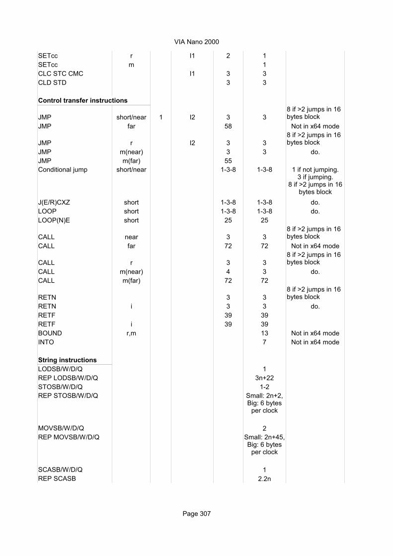
VIA Nano 2000
Page 307
SETcc r I1 2 1SETcc m 1CLC STC CMC I1 3 3CLD STD 3 3
Control transfer instructions
JMP short/near 1 I2 3 3JMP far 58 Not in x64 mode
JMP r I2 3 3JMP m(near) 3 3 do.JMP m(far) 55Conditional jump short/near 1-3-8 1-3-8
J(E/R)CXZ short 1-3-8 1-3-8 do.LOOP short 1-3-8 1-3-8 do.LOOP(N)E short 25 25
CALL near 3 3CALL far 72 72 Not in x64 mode
CALL r 3 3CALL m(near) 4 3 do.CALL m(far) 72 72
RETN 3 3RETN i 3 3 do.RETF 39 39RETF i 39 39BOUND r,m 13 Not in x64 modeINTO 7 Not in x64 mode
String instructionsLODSB/W/D/Q 1REP LODSB/W/D/Q 3n+22STOSB/W/D/Q 1-2REP STOSB/W/D/Q
MOVSB/W/D/Q 2REP MOVSB/W/D/Q
SCASB/W/D/Q 1REP SCASB 2.2n
8 if >2 jumps in 16 bytes block
8 if >2 jumps in 16 bytes block
1 if not jumping.3 if jumping.
8 if >2 jumps in 16 bytes block
8 if >2 jumps in 16 bytes block
8 if >2 jumps in 16 bytes block
8 if >2 jumps in 16 bytes block
Small: 2n+2, Big: 6 bytes
per clock
Small: 2n+45,Big: 6 bytes
per clock

VIA Nano 2000
Page 308
REP SCASW/D/Q
CMPSB/W/D/Q 6REP CMPSB/W/D/Q 2.4n+24
OtherNOP (90) 1 All 1 Blocks all portsLong NOP (0F 1F) 1 I12 1/2PAUSE 25ENTER a,0 23ENTER a,b 52+5bLEAVE 4 4CPUID 53-173RDTSC 39RDPMC 40 40
Floating point x87 instructionsOperands μops Latency Remarks
Move instructionsFLD r 1 MB 1 1FLD m32/m64 2 LD MB 4 1FLD m80 2 LD MB 4 1FBLD m80 54 54FST(P) r 1 MB 1 1FST(P) m32/m64 3 MB SA ST 5 1-2FSTP m80 3 MB SA ST 5 1-2FBSTP m80 125 125FXCH r 1 I2 0 1FILD m16 7FILD m32 5FILD m64 5FIST(T)(P) m16 6FIST(T)(P) m32 5FIST(T)(P) m64 5FLDZ FLD1 1 MB 1FLDPI FLDL2E etc. 10FCMOVcc r 2 2FNSTSW AX 5FNSTSW m16 3FLDCW m16 13 13FNSTCW m16 2FINCSTP FDECSTP 1 I2 0 1FFREE(P) 1 MB 1FNSAVE m 321 321FRSTOR m 195 195
Arithmetic instructions
Small: 2n+50Big: 5 bytes
per clock
Port and Unit
Reciprocal thruoghput
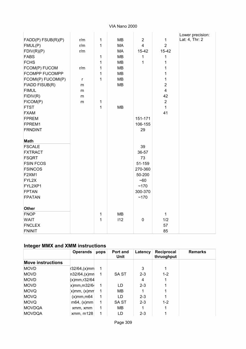
VIA Nano 2000
Page 309
FADD(P) FSUB(R)(P) r/m 1 MB 2 1FMUL(P) r/m 1 MA 4 2FDIV(R)(P) r/m MA 15-42 15-42FABS 1 MB 1 1FCHS 1 MB 1 1FCOM(P) FUCOM r/m 1 MB 1FCOMPP FUCOMPP 1 MB 1FCOMI(P) FUCOMI(P) r 1 MB 1FIADD FISUB(R) m MB 2FIMUL m 4FIDIV(R) m 42FICOM(P) m 1 2FTST 1 MB 1FXAM 41FPREM 151-171FPREM1 106-155FRNDINT 29
MathFSCALE 39FXTRACT 36-57FSQRT 73FSIN FCOS 51-159FSINCOS 270-360F2XM1 50-200FYL2X ~60FYL2XP1 ~170FPTAN 300-370FPATAN ~170
OtherFNOP 1 MB 1WAIT 1 I12 0 1/2FNCLEX 57FNINIT 85
Integer MMX and XMM instructionsOperands μops Latency Remarks
Move instructionsMOVD r32/64,(x)mm 1 3 1MOVD m32/64,(x)mm 1 SA ST 2-3 1-2MOVD (x)mm,r32/64 4 1MOVD (x)mm,m32/64 1 LD 2-3 1MOVQ (x)mm, (x)mm 1 MB 1 1MOVQ (x)mm,m64 1 LD 2-3 1MOVQ m64, (x)mm 1 SA ST 2-3 1-2MOVDQA xmm, xmm 1 MB 1 1MOVDQA xmm, m128 1 LD 2-3 1
Lower precision: Lat: 4, Thr: 2
Port and Unit
Reciprocal thruoghput

VIA Nano 2000
Page 310
MOVDQA m128, xmm 1 SA ST 2-3 1-2MOVDQU m128, xmm 1 SA ST 2-3 1-2MOVDQU xmm, m128 1 LD 2-3 1LDDQU xmm, m128 1 LD 2-3 1MOVDQ2Q mm, xmm 1 MB 1 1MOVQ2DQ xmm,mm 1 MB 1 1MOVNTQ m64,mm 3 ~300 2MOVNTDQ m128,xmm 3 ~300 2
v,v 1 MB 1 1
v,v 1 MB 1 1PUNPCKH/LQDQ v,v 1 MB 1 1PSHUFB v,v 1 MB 1 1PSHUFW mm,mm,i 1 MB 1 1PSHUFL/HW x,x,i 1 MB 1 1PSHUFD x,x,i 1 MB 1 1PALIGNR x,x,i 1 MB 1 1MASKMOVQ mm,mm 1-3MASKMOVDQU xmm,xmm 1-3PMOVMSKB r32,(x)mm 3 1PEXTRW r32 ,(x)mm,i 3 1PINSRW (x)mm,r32,i 9 9
Arithmetic instructionsPADD/SUB(U)(S)B/W/D
v,v 1 MB 1 1PADDQ PSUBQ v,v 1 MB 1 1
v,v 3 MB 3 3PHADDD PHSUBD v,v 3 MB 3 3PCMPEQ/GTB/W/D v,v 1 MB 1 1PMULL/HW PMULHUW v,v 1 MA 3 1PMULHRSW v,v 1 MA 3 1PMULUDQ v,v 1 MA 3 1PMADDWD v,v 4 2PMADDUBSW v,v 10 8PSADBW v,v MB 2 1PAVGB/W v,v 1 MB 1 1PMIN/MAXUB v,v 1 MB 1 1PMIN/MAXSW v,v 1 MB 1 1PABSB PABSW PABSD
v,v 1 MB 1 1
v,v 1 MB 1 1
Logic instructionsPAND(N) POR PXOR v,v 1 MB 1 1PSLL/RL/RAW/D/Q v,v 1 MB 1 1PSLL/RL/RAW/D/Q v,i 1 MB 1 1PSLL/RLDQ x,i 1 MB 1 1
PACKSSWB/DW PACKUSWB
PUNPCKH/LBW/WD/ DQ
PHADD(S)W PHSUB(S)W
PSIGNB PSIGNW PSIGND

VIA Nano 2000
Page 311
OtherEMMS 1 MB 1
Floating point XMM instructionsOperands μops Latency Remarks
Move instructionsMOVAPS/D xmm,xmm 1 MB 1 1MOVAPS/D xmm,m128 1 LD 2-3 1MOVAPS/D m128,xmm 1 SA ST 2-3 1-2MOVUPS/D xmm,m128 1 LD 2-3 1MOVUPS/D m128,xmm 1 SA ST 2-3 1-2MOVSS/D xmm,xmm 1 MB 1 1MOVSS/D x,m32/64 1 LD 2-3 1MOVSS/D m32/64,x 1 SA ST 2-3 1-2MOVHPS/D xmm,m64 6 1MOVLPS/D xmm,m64 6 1MOVHPS/D m64,xmm 6 1-2MOVLPS/D m64,xmm 2 1-2MOVLHPS MOVHLPS xmm,xmm 1 MB 1 1MOVMSKPS/D r32,xmm 3 1MOVNTPS/D m128,xmm ~300 2,5SHUFPS xmm,xmm,i 1 MB 1 1SHUFPD xmm,xmm,i 1 MB 1 1MOVDDUP xmm,xmm 1 MB 1 1MOVSH/LDUP xmm,xmm 1 MB 1 1UNPCKH/LPS xmm,xmm 1 MB 1 1UNPCKH/LPD xmm,xmm 1 MB 1 1
ConversionCVTPD2PS xmm,xmm 3-4CVTSD2SS xmm,xmm 15CVTPS2PD xmm,xmm 3-4CVTSS2SD xmm,xmm 15CVTDQ2PS xmm,xmm 3CVT(T) PS2DQ xmm,xmm 2CVTDQ2PD xmm,xmm 4CVT(T)PD2DQ xmm,xmm 3CVTPI2PS xmm,mm 4CVT(T)PS2PI mm,xmm 3CVTPI2PD xmm,mm 4CVT(T) PD2PI mm,xmm 3CVTSI2SS xmm,r32 5CVT(T)SS2SI r32,xmm 4CVTSI2SD xmm,r32 5CVT(T)SD2SI r32,xmm 4
ArithmeticADDSS SUBSS xmm,xmm 1 MBfadd 2-3 1
Port and Unit
Reciprocal thruoghput

VIA Nano 2000
Page 312
ADDSD SUBSD xmm,xmm 1 MBfadd 2-3 1ADDPS SUBPS xmm,xmm 1 MBfadd 2-3 1ADDPD SUBPD xmm,xmm 1 MBfadd 2-3 1ADDSUBPS xmm,xmm 1 MBfadd 2-3 1ADDSUBPD xmm,xmm 1 MBfadd 2-3 1HADDPS HSUBPS xmm,xmm MBfadd 5 3HADDPD HSUBPD xmm,xmm MBfadd 5 3MULSS xmm,xmm 1 MA 3 1MULSD xmm,xmm 1 MA 4 2MULPS xmm,xmm MA 3 1MULPD xmm,xmm MA 4 2DIVSS xmm,xmm MA 15-22 15-22DIVSD xmm,xmm MA 15-36 15-36DIVPS xmm,xmm MA 42-82 42-82DIVPD xmm,xmm MA 24-70 24-70RCPSS xmm,xmm 5 5RCPPS xmm,xmm 14 11CMPccSS/D xmm,xmm 1 MBfadd 2 1CMPccPS/D xmm,xmm 1 MBfadd 2 1COMISS/D UCOMISS/D
xmm,xmm 3 1MAXSS/D MINSS/D xmm,xmm 1 MBfadd 2 1MAXPS/D MINPS/D xmm,xmm 1 MBfadd 2 1
MathSQRTSS xmm,xmm MA 33 33SQRTPS xmm,xmm MA 126 126SQRTSD xmm,xmm MA 62 62SQRTPD xmm,xmm MA 122 122RSQRTSS xmm,xmm 5 5RSQRTPS xmm,xmm 14 11
LogicANDPS/D xmm,xmm 1 MB 1 1ANDNPS/D xmm,xmm 1 MB 1 1ORPS/D xmm,xmm 1 MB 1 1XORPS/D xmm,xmm 1 MB 1 1
OtherLDMXCSR m32 45 29STMXCSR m32 13 13FXSAVE m4096 208 208FXRSTOR m4096 232 232
VIA-specific instructionsInstruction Conditions Clock cycles, approximatelyXSTORE Data available 160-400 clock giving 8 bytesXSTORE No data available 50-80 clock giving 0 bytesREP XSTORE Quality factor = 0 4800 clock per 8 bytesREP XSTORE Quality factor > 0 19200 clock per 8 bytes

VIA Nano 2000
Page 313
REP XCRYPTECB 128 bits key 44 clock per 16 bytes REP XCRYPTECB 192 bits key 46 clock per 16 bytes REP XCRYPTECB 256 bits key 48 clock per 16 bytes REP XCRYPTCBC 128 bits key 54 clock per 16 bytes REP XCRYPTCBC 192 bits key 59 clock per 16 bytes REP XCRYPTCBC 256 bits key 63 clock per 16 bytes REP XCRYPTCTR 128 bits key 43 clock per 16 bytes REP XCRYPTCTR 192 bits key 46 clock per 16 bytes REP XCRYPTCTR 256 bits key 48 clock per 16 bytes REP XCRYPTCFB 128 bits key 54 clock per 16 bytes REP XCRYPTCFB 192 bits key 59 clock per 16 bytes REP XCRYPTCFB 256 bits key 63 clock per 16 bytes REP XCRYPTOFB 128 bits key 54 clock per 16 bytes REP XCRYPTOFB 192 bits key 59 clock per 16 bytes REP XCRYPTOFB 256 bits key 63 clock per 16 bytes REP XSHA1 3 clock per byteREP XSHA256 4 clock per byte

Nano 3000
Page 314
VIA Nano 3000 seriesList of instruction timings and μop breakdown
Explanation of column headings:Operands:
μops:
Port:
I1: Integer add, Boolean, shift, etc.I2: Integer add, Boolean, move, jump.I12: Can use either I1 or I2, whichever is vacant first.MA: Multiply, divide and square root on all operand types.MB: Various Integer and floating point SIMD operations.MBfadd: Floating point addition subunit under MB.SA: Memory store address.ST: Memory store.LD: Memory load.
Latency:
Reciprocal throughput:
Integer instructionsOperands μops Port Latency Remarks
Move instructionsMOV r,r 1 I2 1 1MOV r,i 1 I12 1 1/2
MOV r,m 1 LD 2 1MOV m,r 1 SA, ST 2 1,5MOV m,i 1 SA, ST 1,5MOV r,sr I12 1/2MOV m,sr 1,5MOV sr,r 20 20
i = immediate data, r = register, mm = 64 bit mmx register, xmm = 128 bit xmm register, (x)mm = mmx or xmm register, sr = segment register, m = memory, m32 = 32-bit memory operand, etc.
The number of micro-operations from the decoder or ROM. Note that the VIA Nano 3000 processor has no reliable performance monitor counter for μops. Therefore the number of μops cannot be determined except in simple cases.
Tells which execution port or unit is used. Instructions that use the same port cannot execute simultaneously.
This is the delay that the instruction generates in a dependency chain. The numbers are minimum values. Cache misses, misalignment, and exceptions may increase the clock counts considerably. Floating point operands are pre-sumed to be normal numbers. Denormal numbers, NAN's and infinity increase the delays very much, except in XMM move, shuffle and Boolean instructions. Floating point overflow, underflow, denormal or NAN results give a similar de-lay.
Note: There is an additional latency for moving data from one unit or subunit to another. A table of these latencies is given in manual 3: "The microarchitec-ture of Intel, AMD and VIA CPUs". These additional latencies are not included in the listings below where the source and destination operands are of the same type.
The average number of clock cycles per instruction for a series of independent instructions of the same kind in the same thread.
Reciprocal thruogh-
put
Latency 4 on pointer register
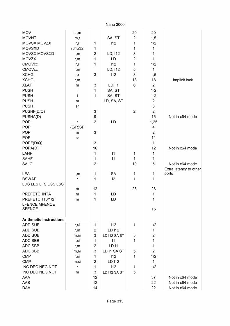
Nano 3000
Page 315
MOV sr,m 20 20MOVNTI m,r SA, ST 2 1,5MOVSX MOVZX r,r 1 I12 1 1/2MOVSXD r64,r32 1 1 1MOVSX MOVSXD r,m 2 LD, I12 3 1MOVZX r,m 1 LD 2 1CMOVcc r,r 1 I12 1 1/2CMOVcc r,m LD, I12 5 1XCHG r,r 3 I12 3 1,5XCHG r,m 18 18 Implicit lockXLAT m 3 LD, I1 6 2PUSH r 1 SA, ST 1-2PUSH i 1 SA, ST 1-2PUSH m LD, SA, ST 2PUSH sr 6PUSHF(D/Q) 3 2 2PUSHA(D) 9 15 Not in x64 modePOP r 2 LD 1,25POP (E/R)SP 4POP m 3 2POP sr 11POPF(D/Q) 3 1POPA(D) 16 12 Not in x64 modeLAHF 1 I1 1 1SAHF 1 I1 1 1SALC 2 10 6 Not in x64 mode
LEA r,m 1 SA 1 1BSWAP r 1 I2 1 1LDS LES LFS LGS LSS
m 12 28 28PREFETCHNTA m 1 LD 1PREFETCHT0/1/2 m 1 LD 1
15
Arithmetic instructionsADD SUB r,r/i 1 I12 1 1/2ADD SUB r,m 2 LD I12 1ADD SUB m,r/i 3 LD I12 SA ST 5 2ADC SBB r,r/i 1 I1 1 1ADC SBB r,m 2 LD I1 1ADC SBB m,r/i 3 LD I1 SA ST 5 2CMP r,r/i 1 I12 1 1/2CMP m,r/i 2 LD I12 1INC DEC NEG NOT r 1 I12 1 1/2INC DEC NEG NOT m 3 LD I12 SA ST 5AAA 12 37 Not in x64 modeAAS 12 22 Not in x64 modeDAA 14 22 Not in x64 mode
Extra latency to other ports
LFENCE MFENCE SFENCE
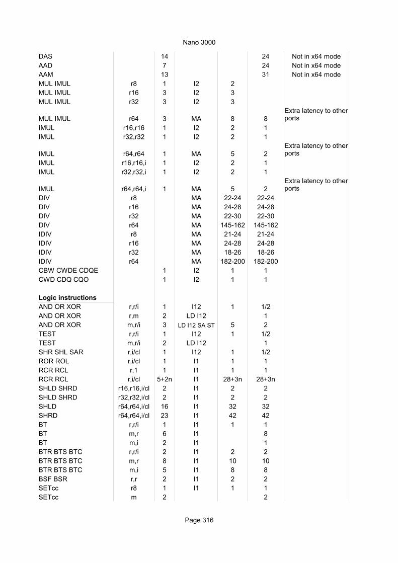
Nano 3000
Page 316
DAS 14 24 Not in x64 modeAAD 7 24 Not in x64 modeAAM 13 31 Not in x64 modeMUL IMUL r8 1 I2 2MUL IMUL r16 3 I2 3MUL IMUL r32 3 I2 3
MUL IMUL r64 3 MA 8 8IMUL r16,r16 1 I2 2 1IMUL r32,r32 1 I2 2 1
IMUL r64,r64 1 MA 5 2IMUL r16,r16,i 1 I2 2 1IMUL r32,r32,i 1 I2 2 1
IMUL r64,r64,i 1 MA 5 2DIV r8 MA 22-24 22-24DIV r16 MA 24-28 24-28DIV r32 MA 22-30 22-30DIV r64 MA 145-162 145-162IDIV r8 MA 21-24 21-24IDIV r16 MA 24-28 24-28IDIV r32 MA 18-26 18-26IDIV r64 MA 182-200 182-200CBW CWDE CDQE 1 I2 1 1CWD CDQ CQO 1 I2 1 1
Logic instructionsAND OR XOR r,r/i 1 I12 1 1/2AND OR XOR r,m 2 LD I12 1AND OR XOR m,r/i 3 LD I12 SA ST 5 2TEST r,r/i 1 I12 1 1/2TEST m,r/i 2 LD I12 1SHR SHL SAR r,i/cl 1 I12 1 1/2ROR ROL r,i/cl 1 I1 1 1RCR RCL r,1 1 I1 1 1RCR RCL r,i/cl 5+2n I1 28+3n 28+3nSHLD SHRD r16,r16,i/cl 2 I1 2 2SHLD SHRD r32,r32,i/cl 2 I1 2 2SHLD r64,r64,i/cl 16 I1 32 32SHRD r64,r64,i/cl 23 I1 42 42BT r,r/i 1 I1 1 1BT m,r 6 I1 8BT m,i 2 I1 1BTR BTS BTC r,r/i 2 I1 2 2BTR BTS BTC m,r 8 I1 10 10BTR BTS BTC m,i 5 I1 8 8BSF BSR r,r 2 I1 2 2SETcc r8 1 I1 1 1SETcc m 2 2
Extra latency to other ports
Extra latency to other ports
Extra latency to other ports

Nano 3000
Page 317
CLC STC CMC 3 I1 3 3CLD STD 3 I1 3 3
Control transfer instructions
JMP short/near 1 I2 3 3JMP far 14 50 Not in x64 mode
JMP r 2 I2 3 3JMP m(near) 2 3 3 do.JMP m(far) 17 42
Conditional jump short/near 1 I2 1-3-8 1-3-8J(E/R)CXZ short 2 1-3-8 1-3-8LOOP short 2 1-3-8 1-3-8LOOP(N)E short 5 24 24
CALL near 2 3 3CALL far 17 58 Not in x64 mode
CALL r 2 3 3CALL m(near) 3 4 3 do.CALL m(far) 19 54
RETN 3 3 3RETN i 4 3 3 do.RETF 20 49RETF i 20 49BOUND r,m 9 13 Not in x64 modeINTO 3 7 Not in x64 mode
String instructionsLODSB/W/D/Q 2 1REP LODSB/W/D/Q 3n 3n+27STOSB/W/D/Q 1 1-2
REP STOSB/W/D/QMOVSB/W/D/Q 3 2
REP MOVSB/W/D/QSCASB/W/D/Q 3 1REP SCASB 2.4n
REP SCASW/D/Q
8 if >2 jumps in 16 bytes block
8 if >2 jumps in 16 bytes block
1 if not jumping.3 if jumping.8 if >2 jumps in 16 bytes block
8 if >2 jumps in 16 bytes block
8 if >2 jumps in 16 bytes block
8 if >2 jumps in 16 bytes block
Small: n+40, Big: 6-7 bytes/clk
Small: 2n+20,Big: 6-7 bytes/clk
Small: 2n+31,Big: 5 bytes/clk

Nano 3000
Page 318
CMPSB/W/D/Q 5 6REP CMPSB/W/D/Q 2.2n+30
OtherNOP (90) 0-1 I12 0 1/2 Sometimes fusedlong NOP (0F 1F) 0-1 I12 0 1/2PAUSE 2 6ENTER a,0 10 21ENTER a,b 52+5bLEAVE 3 2 2CPUID 55-146RDTSC 37RDPMC 40
Floating point x87 instructionsOperands μops Port Latency Remarks
Move instructionsFLD r 1 MB 1 1FLD m32/m64 2 LD MB 4 1FLD m80 2 LD MB 4 1FBLD m80 36 54 54FST(P) r 1 MB 1 1FST(P) m32/m64 3 MB SA ST 5 1-2FSTP m80 3 MB SA ST 5 1-2FBSTP m80 80 125 125FXCH r 1 I2 0 1FILD m16 3 7FILD m32 2 5FILD m64 2 5FIST(T)(P) m16 3 6FIST(T)(P) m32 3 5FIST(T)(P) m64 3 5FLDZ FLD1 1 MB 1FLDPI FLDL2E etc. 3 10FCMOVcc r 1 MB 2 2FNSTSW AX 1 1FNSTSW m16 3 2FLDCW m16 5 8FNSTCW m16 3 2FINCSTP FDECSTP 1 I2 0 1FFREE(P) 1 MB 1FNSAVE m 122 319 319FRSTOR m 115 196 196
Arithmetic instructionsFADD(P) FSUB(R)(P) r/m 1 MB 2 1
Reciprocal thruogh-
put
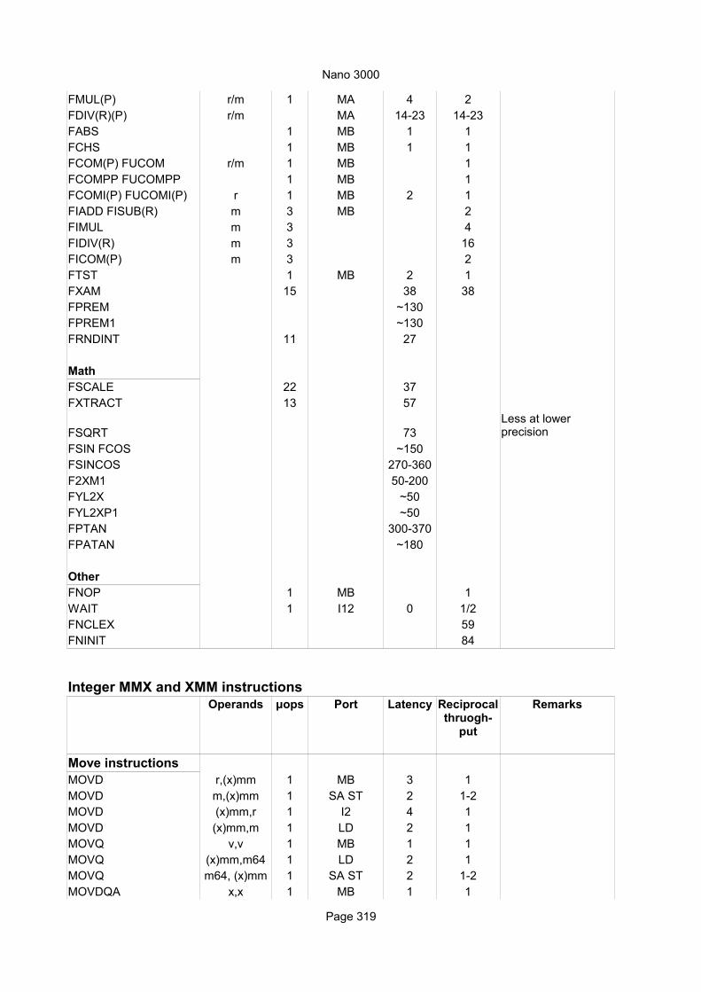
Nano 3000
Page 319
FMUL(P) r/m 1 MA 4 2FDIV(R)(P) r/m MA 14-23 14-23FABS 1 MB 1 1FCHS 1 MB 1 1FCOM(P) FUCOM r/m 1 MB 1FCOMPP FUCOMPP 1 MB 1FCOMI(P) FUCOMI(P) r 1 MB 2 1FIADD FISUB(R) m 3 MB 2FIMUL m 3 4FIDIV(R) m 3 16FICOM(P) m 3 2FTST 1 MB 2 1FXAM 15 38 38FPREM ~130FPREM1 ~130FRNDINT 11 27
MathFSCALE 22 37FXTRACT 13 57
FSQRT 73FSIN FCOS ~150FSINCOS 270-360F2XM1 50-200FYL2X ~50FYL2XP1 ~50FPTAN 300-370FPATAN ~180
OtherFNOP 1 MB 1WAIT 1 I12 0 1/2FNCLEX 59FNINIT 84
Integer MMX and XMM instructionsOperands μops Port Latency Remarks
Move instructionsMOVD r,(x)mm 1 MB 3 1MOVD m,(x)mm 1 SA ST 2 1-2MOVD (x)mm,r 1 I2 4 1MOVD (x)mm,m 1 LD 2 1MOVQ v,v 1 MB 1 1MOVQ (x)mm,m64 1 LD 2 1MOVQ m64, (x)mm 1 SA ST 2 1-2MOVDQA x,x 1 MB 1 1
Less at lower precision
Reciprocal thruogh-
put

Nano 3000
Page 320
MOVDQA x, m128 1 LD 2 1MOVDQA m128, x 1 SA ST 2 1-2MOVDQU m128, x 1 SA ST 2 1-2MOVDQU x, m128 1 LD 2 1LDDQU x, m128 1 LD 2 1MOVDQ2Q mm, x 1 MB 1 1MOVQ2DQ x,mm 1 MB 1 1MOVNTQ m64,mm 2 ~360 2MOVNTDQ m128,x 2 ~360 2MOVNTDQA x,m128 1 2 1
v,v 1 MB 1 1PACKUSDW x,x 1 MB 1 1PUNPCKH/LBW/WD/DQ v,v 1 MB 1 1PUNPCKH/LQDQ v,v 1 MB 1 1PSHUFB v,v 1 MB 1 1PSHUFW mm,mm,i 1 MB 1 1PSHUFL/HW x,x,i 1 MB 1 1PSHUFD x,x,i 1 MB 1 1PBLENDVB x,x,xmm0 1 MB 2 2PBLENDW x,x,i 1 MB 1 1PALIGNR x,x,i 1 MB 1 1MASKMOVQ mm,mm 1-2MASKMOVDQU x,x 1-2PMOVMSKB r32,(x)mm 3 1PEXTRW r32 ,(x)mm,i 1 MB 3 1PEXTRB/D/Q r32/64,x,i 1 MB 3 1PINSRW (x)mm,r32,i 2 MB 5 1PINSRB/D/Q x,r32/64,i 2 MB 5 1
x,x 1 MB 1 1
Arithmetic instructionsPADD/SUB(U)(S)B/W/D
v,v 1 MB 1 1PADDQ PSUBQ v,v 1 MB 1 1
v,v 3 MB 3 3PHADDD PHSUBD v,v 3 MB 3 3PCMPEQ/GTB/W/D v,v 1 MB 1 1PCMPEQQ x,x 1 MB 1 1PMULL/HW PMULHUW v,v 1 MA 3 1PMULHRSW v,v 1 MA 3 1PMULLD x,x 1 MA 3 1PMULUDQ v,v 1 MA 3 1PMULDQ x,x 1 MA 3 1PMADDWD v,v 1 MA 4 2PMADDUBSW v,v 7 10 8PSADBW v,v 1 MB 2 1MPSADBW x,x,i 1 MB 2 1PAVGB/W v,v 1 MB 1 1
PACKSSWB/DW PACKUSWB
PMOVSX/ZXBW/BD/BQ/WD/WQ/DQ
PHADD(S)W PHSUB(S)W
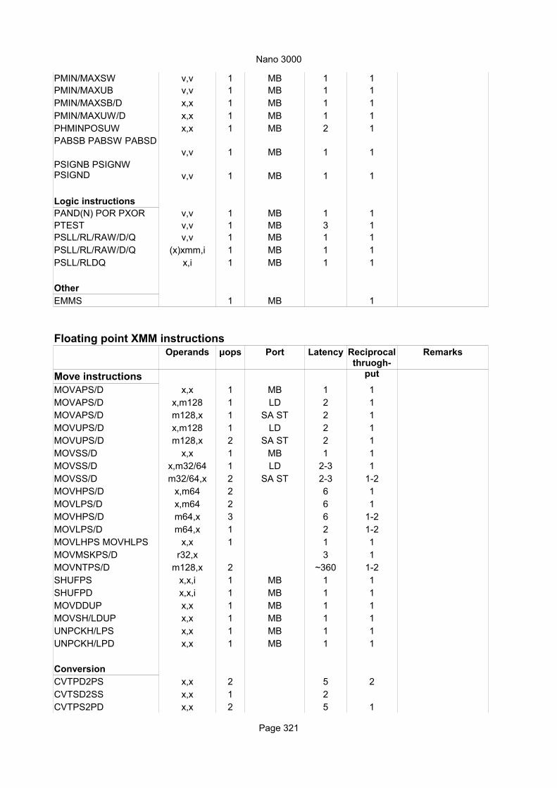
Nano 3000
Page 321
PMIN/MAXSW v,v 1 MB 1 1PMIN/MAXUB v,v 1 MB 1 1PMIN/MAXSB/D x,x 1 MB 1 1PMIN/MAXUW/D x,x 1 MB 1 1PHMINPOSUW x,x 1 MB 2 1PABSB PABSW PABSD
v,v 1 MB 1 1
v,v 1 MB 1 1
Logic instructionsPAND(N) POR PXOR v,v 1 MB 1 1PTEST v,v 1 MB 3 1PSLL/RL/RAW/D/Q v,v 1 MB 1 1PSLL/RL/RAW/D/Q (x)xmm,i 1 MB 1 1PSLL/RLDQ x,i 1 MB 1 1
OtherEMMS 1 MB 1
Floating point XMM instructionsOperands μops Port Latency Remarks
Move instructionsMOVAPS/D x,x 1 MB 1 1MOVAPS/D x,m128 1 LD 2 1MOVAPS/D m128,x 1 SA ST 2 1MOVUPS/D x,m128 1 LD 2 1MOVUPS/D m128,x 2 SA ST 2 1MOVSS/D x,x 1 MB 1 1MOVSS/D x,m32/64 1 LD 2-3 1MOVSS/D m32/64,x 2 SA ST 2-3 1-2MOVHPS/D x,m64 2 6 1MOVLPS/D x,m64 2 6 1MOVHPS/D m64,x 3 6 1-2MOVLPS/D m64,x 1 2 1-2MOVLHPS MOVHLPS x,x 1 1 1MOVMSKPS/D r32,x 3 1MOVNTPS/D m128,x 2 ~360 1-2SHUFPS x,x,i 1 MB 1 1SHUFPD x,x,i 1 MB 1 1MOVDDUP x,x 1 MB 1 1MOVSH/LDUP x,x 1 MB 1 1UNPCKH/LPS x,x 1 MB 1 1UNPCKH/LPD x,x 1 MB 1 1
ConversionCVTPD2PS x,x 2 5 2CVTSD2SS x,x 1 2CVTPS2PD x,x 2 5 1
PSIGNB PSIGNW PSIGND
Reciprocal thruogh-
put

Nano 3000
Page 322
CVTSS2SD x,x 1 2CVTDQ2PS x,x 1 MB 3 1CVT(T) PS2DQ x,x 1 2 1CVTDQ2PD x,x 2 5 1CVT(T)PD2DQ x,x 4 2CVTPI2PS x,mm 2 5 2CVT(T)PS2PI mm,x 1 4 1CVTPI2PD x,mm 2 4 1CVT(T) PD2PI mm,x 2 4 2CVTSI2SS x,r32 2 5CVT(T)SS2SI r32,x 1 4 1CVTSI2SD x,r32 2 5CVT(T)SD2SI r32,x 1 4 1
ArithmeticADDSS SUBSS x,x 1 MBfadd 2 1ADDSD SUBSD x,x 1 MBfadd 2 1ADDPS SUBPS x,x 1 MBfadd 2 1ADDPD SUBPD x,x 1 MBfadd 2 1ADDSUBPS x,x 1 MBfadd 2 1ADDSUBPD x,x 1 MBfadd 2 1HADDPS HSUBPS x,x 3 MBfadd 5 3HADDPD HSUBPD x,x 3 MBfadd 5 3MULSS x,x 1 MA 3 1MULSD x,x 1 MA 4 2MULPS x,x 1 MA 3 1MULPD x,x 1 MA 4 2DIVSS x,x 1 MA 13 13DIVSD x,x 1 MA 13-20 13-20DIVPS x,x 1 MA 24 24DIVPD x,x 1 MA 21-38 21-38RCPSS x,x 1 MA 5 5RCPPS x,x 3 MA 14 11CMPccSS/D x,x 1 MBfadd 2 1CMPccPS/D x,x 1 MBfadd 2 1COMISS/D UCOMISS/D
x,x 1 MBfadd 3 1MAXSS/D MINSS/D x,x 1 MBfadd 2 1MAXPS/D MINPS/D x,x 1 MBfadd 2 1
MathSQRTSS x,x 1 MA 33 33SQRTPS x,x 1 MA 64 64SQRTSD x,x 1 MA 62 62SQRTPD x,x 1 MA 122 122RSQRTSS x,x 1 5 5RSQRTPS x,x 3 14 11
LogicANDPS/D x,x 1 MB 1 1
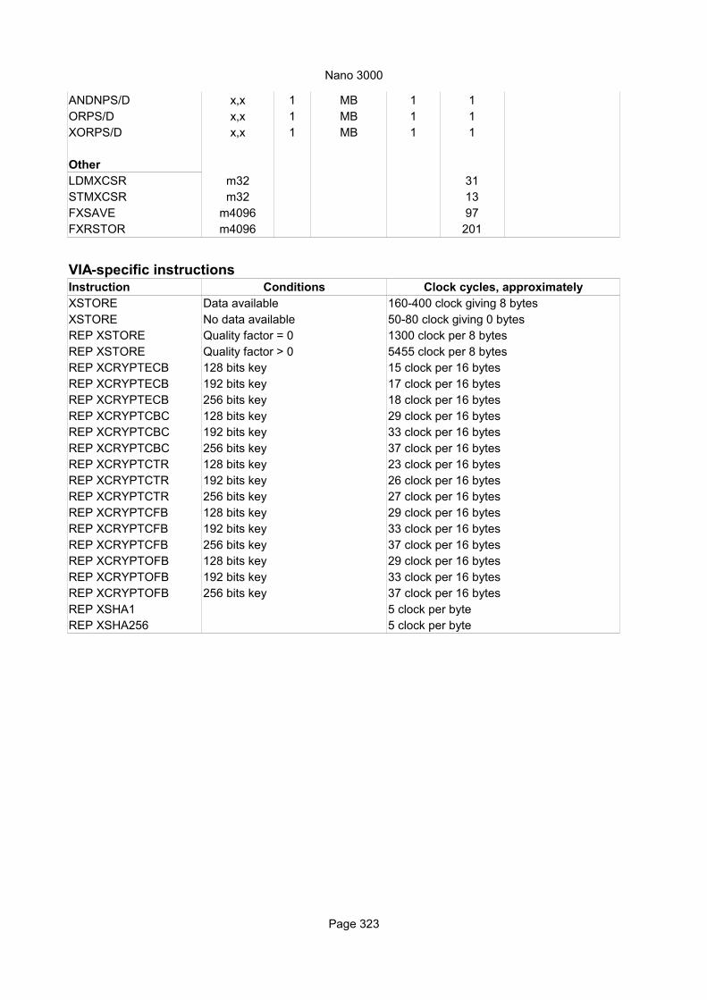
Nano 3000
Page 323
ANDNPS/D x,x 1 MB 1 1ORPS/D x,x 1 MB 1 1XORPS/D x,x 1 MB 1 1
OtherLDMXCSR m32 31STMXCSR m32 13FXSAVE m4096 97FXRSTOR m4096 201
VIA-specific instructionsInstruction Conditions Clock cycles, approximatelyXSTORE Data available 160-400 clock giving 8 bytesXSTORE No data available 50-80 clock giving 0 bytesREP XSTORE Quality factor = 0 1300 clock per 8 bytesREP XSTORE Quality factor > 0 5455 clock per 8 bytesREP XCRYPTECB 128 bits key 15 clock per 16 bytes REP XCRYPTECB 192 bits key 17 clock per 16 bytes REP XCRYPTECB 256 bits key 18 clock per 16 bytes REP XCRYPTCBC 128 bits key 29 clock per 16 bytes REP XCRYPTCBC 192 bits key 33 clock per 16 bytes REP XCRYPTCBC 256 bits key 37 clock per 16 bytes REP XCRYPTCTR 128 bits key 23 clock per 16 bytes REP XCRYPTCTR 192 bits key 26 clock per 16 bytes REP XCRYPTCTR 256 bits key 27 clock per 16 bytes REP XCRYPTCFB 128 bits key 29 clock per 16 bytes REP XCRYPTCFB 192 bits key 33 clock per 16 bytes REP XCRYPTCFB 256 bits key 37 clock per 16 bytes REP XCRYPTOFB 128 bits key 29 clock per 16 bytes REP XCRYPTOFB 192 bits key 33 clock per 16 bytes REP XCRYPTOFB 256 bits key 37 clock per 16 bytes REP XSHA1 5 clock per byteREP XSHA256 5 clock per byte