3rd generation solar cells - latest seminar topics for ...€¦ · 2nd nordic workshop on...
TRANSCRIPT
3/25/08
Status report:
Silicon-based 3rd generation solar cells
Erik Stensrud MarsteinJ.E. Fonneløp, S.E Foss, A. Holt, S. Karazhanov, J.P. Mæhlen, J.H. Selj, A.G.
Ulyashin and D.N. Wright, IFE
2nd Nordic Workshop on Crystalline Silicon Solar CellsMarch 5.-6., Narvik, Norway

3/25/08
Overview
• The trouble with conventional silicon-based solar cells
• 3rd generation solar cell concepts
• Status report: 3rd generation solar cells made from silicon• Photon energy conversion
• Multi-junction solar cells
• Ongoing research at IFE

3/25/08
Too keep things straight…
• ”Normal” crystalline Si homojunction solar cells are NOT badsolar cells!
• Best crystalline Si solar cell efficiency: 24.7% (1 Sun)
• Best large area Si-based solar cell: ~ 22%
• Best large area Si-based solar module: ~ 20%
• Current market share: > 90%
• Energy payback times (solar energy system): ~ 3 years
• Non-toxic and abundant raw materials
• …

3/25/08
However…
• Sunlight consists of a large numberof photons distributed across alarge wavelength range.
• The photon energy depends on thephoton wavelength in the followingmanner:
Ephot = hc/λ
• The variation in photon energymakes efficient utilization of theentire solar spectrum in one solarcell difficult.
0
200
400
600
800
1000
1200
1400
1600
1800
0 1 2 3 4 5
Wavelength [um]Ir
radia
nce

3/25/08
Homo-junction solar cells
• Conventional solar cells are madefrom one material and utilize oneelectronic band gap.
• Band gap energy Eg
• Homo-junction solar cell: solarcell with the p-n junction built intoone material.
• Prime example: crystalline Si solarcells
Eg

3/25/08
Homo-junction solar cells
• A photon with sufficient energy canexcite an electron across the band gapcreating a mobile electron and a mobilehole.
• If the photogenerated electron and holeare collected at the external solar cellterminals, they will contribute to thecurrent from the solar cell.
• The voltage related to this process isdetermined by the energy difference atwhich the electron and hole can beextracted at the external terminals.
Ephot
-
+
EgqV = Ephot

3/25/08
The trouble with homo-junction solar cells
• Only photons with sufficientenergy can excite e- across theband gap Eg.
• Insufficiently energetic photonswith Ephot < Eg will not contributeto the photocurrent generation (1).
• Photons with Ephot > Eg will initiallygenerate energetic excited chargecarriers (2).
• Any energy in excess of Eg will bewasted heating up the solar cellthrough thermalization (3).
Ephot
1
-
+2
Eg
3
-
+
qV < Eg

3/25/08
Thermalization
• Thermalization within solar cellmaterials normally occurs on anextremely rapid time scale
• Thermalization in Si:1: Initial concentration of charge
carriers2: Initial exitation of charge carriers
after exposure to laser pulse3-4:Carrier-carrier collisions lead to
an energetic redistribution aroundcarrier temperature
5-6:Carrier-phonon interactions cooldown carriers
7-8:Recombination across band gapM.A. Green, UNSW

3/25/08
ConsequencesNON-OPTIMAL UTILIZATION
OF PHOTON ENERGIESLOST PHOTONS

3/25/08
Consequences
• Large current densities can be obtained by selecting a materialwith a low band gap energy
• However, due to thermalization, the band gap puts an efficientupper limit to the extractable voltage.
• If we should be even so lucky!• Si bandgap: 1.12 eV
• Good open circuit voltage: 700 mV

3/25/08
The Shockley-Queisser limit
• The Shockley-Queisser limit is a measure of the upper obtainable efficiency ofa perfect solar cell based on only one solar cell material with only oneelectronic band gap.
• Main assumptions:• All photons incident on cell captured• Complete absorption of all photons with E > Eg• Complete thermalization occurs• Lossless transport and collection of charge carriers• Ideal materials: Only Auger or radiative recombination
• The very best homo-junctions can in principle reach ~33%• The efficiency limit of a perfect Si homo-junction solar cell is ~ 30%

3/25/08
The Shockley-Queisser limit
• Upper limit for homo-junction efficiency: 33%
• Where do the remaining 67% go?
M.C. Beard et al., Nano Letters 7 (2007) p 2506
100%Total
33%Remaining efficiency
1.5%Recombination
18.5%Transmission (E < Eg)
47%Thermalization (E > Eg)

3/25/08
3rd generation photovoltaics
• Useful definition: ”Solar cell concepts that allow for a moreefficient utilization of the sunlight than homo-junction solar cells.”
• Main approaches:• Modification of the photonic energy distribution prior to absorption in a
solar cell
• Utilization of materials or cell structures incorporating several band gaps
• Reducing losses due to thermalization• Hot carrier solar cells
• Impact ionization solar cells

3/25/08
3rd generation Si solar cells
• Modification of the photonic energy distribution prior toabsorption in a solar cell• Photon energy down-conversion
• Photon energy up-conversion
• Utilization of materials or cell structures incorporating severalband gaps• Si-based multi-junction solar cells

3/25/08
3rd generation Si solar cells
• Impact ionization of little use in Si solar cells• Treshold energy: 3.5 Eg (3.9 eV ~ 315 nm)
• Quantum yield (QY): 1.4 at 4.5 Eg (5.0 eV ~ 250 nm)
e-
e-e-
e-
e-

3/25/08
Modifying the photon energy distribution
• Photon energy down-conversion:one energetic photon creates morethan one sufficiently energeticphoton.
• Photon energy up-conversion: twoor more low energetic photonscreate one sufficiently energeticphoton.
Down-conversion
Up-conversion
Eg
Eg2 Eg
Eg½ Eg
½ Eg

3/25/08
Photon energy down-conversion on Si
• The “pixie dust” approach: simplyadd photon energy down-conversion materials in front of thesolar cell
• Anti-reflection coating
• Transparent conductive layer
• Laminates
• Cover glass
• Separate layer (plan B)
• Theoretical efficiency on Si: 38.6%
Down-conversion solution for Si solar cell
B.S. Richards et al., Sol. En. Mat. and Sol. Cells 90 (2006) p. 1189

3/25/08
Real world challenges• Suitable materials must efficiently
absorb high energy photons and reemitmore than one photon with sufficientenergies for use in Si solar cell
• 2 Eg = 2.2 eV (~ 550 nm)
• Suitable materials must also betransparent for photons of lowerenergies in order to not disturbutilization of this large part of the solarspectrum
• ~15% of the emitted photons willescape from a material with n = 1.5
• Light trapping?
2 Eg Eg
3/25/08
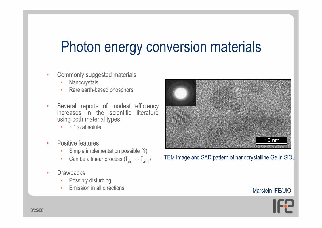
Photon energy conversion materials
• Commonly suggested materials• Nanocrystals• Rare earth-based phosphors
• Several reports of modest efficiencyincreases in the scientific literatureusing both material types
• ~ 1% absolute
• Positive features• Simple implementation possible (?)• Can be a linear process (Iem ~ Iabs)
• Drawbacks• Possibly disturbing• Emission in all directions Marstein IFE/UiO
TEM image and SAD pattern of nanocrystalline Ge in SiO2

3/25/08
Multiple exciton generation
• Substantial efficiency gains require multiple exciton generation (MEG)
• MEG has been reported from a range of nanocrystalline semiconductors
• Recent work on 9.5 nm diameter colloidal Si nanocrystals at NREL:• Eg = 1.2 eV
• QY: 2.6 ± 0.2 at 3.4 Eg
• Obtainable efficiency at this energy: 41%
• However, hitherto, photocurrent measurements give QY < 1!
• Dissociation of excitons into photons or mobile charge carriers for subsequentcollection is presently a big challenge
M.C. Beard et al., Nano Letters 7 (2007) p 2506

3/25/08
Photoluminescence
• Photoluminescence (PL) is noroute beyond the Shockley-Queisser limit
• QY < 1
• However, PL might give efficiencyincreases on Si solar cells withlimited blue reponse
Marstein IFE/UiO
EQE of commercial solar cell and PLspectrum from porous Si
Photoluminescence from porous Si
0,00
0,10
0,20
0,30
0,40
0,50
0,60
0,70
0,80
0,90
1,00
0 200 400 600 800 1000 1200 1400
Wavelength [nm]
PL
[a
.u.]
an
d E
QE
[%
]
EQE
PL intensity

3/25/08
Photon energy up conversion on Si
• Photon energy up-conversion onthe rear of the solar cell
• Surface passivating dielectric
• Rear side dielectric mirror
• Separate layer (plan B)
• Theoretical efficiency on Si: 40.2%
Up-conversion solution for Si solarcell
A Shalav et al, APL 86 (2005) p.013505

3/25/08
Photon energy up-conversion materials
• Different material systems tested• Nanocrystals• Rare earth containing phosphors
• Several authors report non-zero EQE values in sub-band gap light• Example: EQE ~ 2,5% (IQE ~ 4%) at 1523 nm (~0.8 eV )(NaYF4:Er3+)
• Positive features• Synthesis of phosphor materials with wide selection of properties possible• Readily integratable in a Si solar cell in a non-disturbing manner• Rear reflectors can be added
• Negative features• Re-emission of sub-band gap light a possibility• Typically a non-linear process: Iem ~ Iabs
2 (2-step)A Shalav et al, APL 86 (2005) p.013505

3/25/08
Multiple band gap solar cells
• Multiple band gap solar cells can berealized in a number of ways
• Physical splitting of the solarspectrum onto different solar cells
• Recent effort: DARPA (a)
• Tandem/multi-junction solar cells• Current world record holder!
• > 40% efficient!• Two or more terminals (b)
• Industry standard in Si thin film solarcell production
• Record efficiency: 12.1%(a-Si/a-Si/a-SiGe, stabilized)

3/25/08
Multi-junction Si solar cells
• Several materials have been grown onto Si substrates byheteroepitaxy• III-V semiconductors
• CIGS
• …
• Efficient Si-based multijunction solar cells have been made• AlGaAs/Si tandem: 21.4%
• Efficiency potential: (1.12 + 1.75 eV): 32%
M. Umeno et al. Solar En. Mat and S.C. 41/42 (1996) p.395

3/25/08
Monolithic multi-junction Si solar cells
• General 3-junction cell: 63%• 0.61 + 1.15 + 1.82 eV
• Direct sunlight
• ”Unconstrained”• Individual connectors to each
subcell
• General 4-junction cell: 53%• 0.72 + 1.10 + 1.53 + 2.14 eV
• Diffuse sunlight
• ”Series constrained”• Current matched subcells
M.A. Green, “Third generation photovoltaics
Unconstrained multi-junction solar cell
Series constrained multi-junction solar cell

3/25/08
A new substrate for multi-junction solar cells
• Concentrators are experiencing areneissance
• Example: GaInP:GaInAs:Ge
• Ge substrates a possible limitingfactor for large scale deployment
• Solution: Si as a substitutionalsubstrate?
A Feltrin and A Freundlich, Renewable Energy 33 (2008) p. 180

3/25/08
Solar cell research at IFE
• Still growing…
• Involved research staff• Solar energy department (’08)
• Personnel: 20 (Q2 2008)
• Other departments• Personnel: 5 + (Q2 2008)
• New solar cell laboratory buildingunder construction

3/25/08
Solar cell research at IFE
• A complete R&D process line for Siwafer-based solar cells
• Well-equipped solar cell and materialcharacterization laboratories
• Recent additions:• Large-area sputtering (Q2 2008)
• Leybold
• New PECVD reactor (Q2 2008)• Oxford Plasmalab 133
• Variable angle spectral ellipsometer• Woollam

3/25/08
3rd generation solar cell research at IFE
• Use of Si substrates as a basis for3rd generation solar cells
• Use of techniques with potential formass-production of large areastructures
• Every single percent is valuable!

3/25/08
3rd generation research topics at IFE
• Synthesis and modeling of newmaterials
• Semiconductor nanocrystals• New, compound semiconductors• Phosphor materials
• Solar cell design and modeling• Concept evaluation
• New processes for thin and highlyefficient Si-based solar cells
• ”Soft” processing• Light trapping

3/25/08
Project example
Thin and highly efficient Si-based solar cells incorporating nanostructures
• Project type: ISP-project in the NANOMAT-programme
• Funding: 31 MNOK
• Project period: 2007-2013
• Goals: 1: To develop a technology platform for production offuture 3rd generation solar cells from Si substrates
2: To develop new, nanostructured materials allowingfor a better utilization of sunlight

3/25/08
Final remarks
• Si solar cells will remain the industry standard for years to come
• Several 3rd generation concepts are of great interest for use in Sisolar cells
• No crystalline Si solar cell utilizing such consepts has been ableto beat the records for high efficiency Si solar cells• No appreciable efficiency increase has been demonstrated
• The best is yet to come!
• IFE has started several research projects within this veryinteresting and fun field

3/25/08
More information?
www.ife.no -> Solenergi
Thank you for your attention!