3d printer electronics design
TRANSCRIPT

End of Bachelor
Bachelor Degree in Industrial Technology
3D PRINTER ELECTRONICS DESIGN
ANNEX
ANNEX I: Visits
ANNEX II: Prototype Cost
ANNEX III: Firmware
ANNEX IV: Datasheets
Author: Isabel Cañete Vela
Director: Emilio Angulo Navarro
Convocatory: July, 2014
Escola Tècnica Superior d’Enginyeria
Industrial de Barcelona

3D Printer Electronics Design
TABLE OF CONTENTS
ANNEX I_Visits ............................................................................................................. 2
I.1 RepRap ETSEIB visit .............................................................................................................. 2
I.2 Fundació CIM Visit ................................................................................................................ 3
Interview ............................................................................................................................... 3
I.3 Fundació CIM visit (II) ........................................................................................................... 5
ANNEX II_Prototype Cost............................................................................................ 7
ANNEX III_FIRMWARE .................................................................................................. 8
Configuration file ................................................................................................................... 8
Pin file .................................................................................................................................. 12
ANNEX IV_Datasheets .............................................................................................. 14
IV.1 ATmega1280 Reference Design
IV.2 Drivers
IV.2.1 A4988
IV.2.2 DRV8825
IV.3 MOSFETs
IV.3.1 IRFB3004PBF
IV.3.2 STP55NF06L
IV.3.3 IRF530
IV. 4 LED LTL-307GE
IV.5 Thermistor 100k EPCOS

2 Bachelor Thesis
ANNEX I_VISITS
I.1 REPRAP ETSEIB VISIT
On 13th of February 2014, it was realized a visit to RepRap printing classroom
localized in ETSEIB. During this visit, it was delved into issues related printer
failures that Sebas Chavez-Ferrer Marcos has found, as well as aspects for
improvement of available printers.
Also, it was evaluated two printer models of the classroom, and it was
performed few comparisons between the first and the third model created
from CIM foundation.
These failures, features and advantages of the third model about the first have
been shown on the A.1 Table. In this table it was abstracted the principal
problems and if it problems has been solved thanks to the last model of RepRap
printer.
General problems First model Third model
Harnessing the print area Not harness the height. Harness the height but
the structure is higher.
Clog at the mouthpiece Frequent Frequent
Mouthpiece change (in
consequence of the
clog)
Hard change. It’s
necessary disassemble a
lot of pieces.
Improved. Although, it
remains a slow process.
Calibration of the table Complicate, it realize by
4 points.
Improved. It realize by 3
points.
Roller support. Non-existent Only available for a coil
model.
Heating Not solved Not solved
Component failures Not solved and the error
it’s hard to localize
Not solved and the error
it’s hard to localize
Table 1. RepRapBCN troubleshooting

3D Printer Electronics Design 3
Figure 1: First and third RepRapBCN models
I.2 FUNDACIÓ CIM VISIT
On 18th of February 2014, it has been realized a visit to the Fundació CIM, entity
attached to the UPC. As described in web " the institutional mission is to transfer
knowledge of engineering and technology management and provide the tools
for businesses and professionals they can create and improve its products and
manufacturing processes [...] getting high technological competitiveness. [...]
This it is done by generating product and process technology by conducting
projects R + D + i ".
Since diffuser character, of innovation and continuous improvement, it was
performed a site visit in order to, first, find the source of this and second,
technology used in 3D printers and possible improvements that could be made.
Therefore, it was realized an interview by one of founders, Joan Calvet
Vivancos, together with some of those responsible for RepRap BCN, Xavi
Martínez Faneca.
INTERVIEW
First, it was only Joan, Sara and Isabel:
- Joan, we know that you’re one of the founders of Fundació CIM. ¿How
and when was it created?
Joan Vivancos: It was created about 1989 y 1990. The state allocated a
budget to creation of a laboratory, which eventually Rector Gabriel Ferrate
Pascual decided to create a laboratory for manufacturing, because the
university did not have any at the time. Finally, was my work and of professor

4 Bachelor Thesis
Ferrer to decide what material would be bought for the laboratory. In those
years, it was begun to use the 'CN machines' but the main problem that had
the business was that they hadn't communication between them. So, instead of
asking Germany the 'turnkey' factory, we chose to take different machines and
meet the problems faced by companies and try to fix them.
- ¿What has been the trajectory of the Fundació CIM over the years?
Fundació CIM experienced a great progress up to arrive to a higher point with
a large number of workers. Came up the crisis, the company it was forced to
join other companies and was converted to what it is now.
Nowadays, we don’t dispose of a high number of fix workers. Only are 40
persons. The rest of the integrants are composed approximately for 160
scholars, a hundred of this in exterior business.
- ¿What is the Fundació CIM and where does the name come from?
It’s an entity that has three principal pillars: formation, services to industry and
investigations. This name has two meanings. The first is the acronym of CIM
(Computer Integrated Manufactuging) and the second it the meaning in
Spanish. The “CIM” represents the high point of a mountain. And that’s our
objective, to climb up the higher point.
When Xavi came, Joan speaks in and did the first question:
- (J.V.) ¿What is the process of realize a CAD design to a solid design?
First, it must design the piece with any software of CAD (SolidWorks, Rinhoceros,
3D Studio…). After, it transfers the archive at STL. This is an archive defined by
face and points. Next, it uses the program Slic3r to pass archives at G-Code.
This is the program that uses the Fundació CIM, but others such as Cura are
used.
Sometimes is necessary too to do a middle pass because appears problems on
the STL archive. The Fundació CIM it uses NetFabb. This is a program that finds
disappeared faces or bad orientations.
Once you have the instructions on G-Code is the time for the hardware of the
printer, which in the present case is the Arduino, which through Marlin
interpreting the actions of G-Code sends shares engines and the drivers
through sensors and a RAMP.
- ¿What are the most common problems in electronics and why it uses
Arduino+RAMPS+Drivers instead of a motherboard with all integrated?
X.M.: The main problems are that drivers are burned. I never would do it on the
same plate because that would throw the whole plate. Next, sometimes RAMPS

3D Printer Electronics Design 5
burned too because pass a lot of intensity to quickly for warm the bed. I don't
know if it is our problem or in electronics. Another important problem is the
warming.
- We are thinking of doing this in hot bed, for the benefits it brings, and
include a temperature and humidity sensor on the plate. Is there any reason
that is not made in hot bed?
X.M.: I think it's a great idea to integrate the sensor. The main drawback is that it
heats everything equally and therefore all parts that currently are made with 3D
printers should be made with PVC or a material that hold heat better, and if
you do it with other material is possible to lose the reproducibility.
- The fact that the structure of all printers is triangular in shape supposes an
advantage?
X.M.: The first printer of this type was carried out with this type of structure, since
then has remained as it is an identifier of the "brand", but now it tends to square
structures.
- We've been told that attachment of the mouthpiece is not the best. ¿have
introduced any changes in this aspect in the latest model of printer?
X.M.: Yes, there have been changes in the shape of the mouthpiece because it
has to keep the solid material to point for melt it quickly and completely. The
only difference about our printer from the rest is that we have managed to do
one of the shorter interior parts. Moreover, all tend to have the same shape.
As for the subjection, it has been projects trying to make it easier to change the
mouthpiece, because becomes clogged as easily. But it’s for this reason that
the mouthpiece must have the minimum game, so all models are screwed.
I.3 FUNDACIÓ CIM VISIT (II)
On 7th of March 2014, Isabel Cañete made another visit to the Fundació CIM. It
was held an interview with Marc Cobler worker area R + D + I of this centre. The
topics of the conversation were based on electronic printers to study what
were the possible failures of these parts and what possible solutions could be
found.
It was determined the following requirements about electronics:
It must be placed all the electronics in the same area of the motherboard to
make it easier to cool. A small fan cools these parts. If these parts are located
on different parts of the plate, the cooling fan does not reach all parts.

6 Bachelor Thesis
Therefore, all must be in the same area so that the small fan cools all the
components.
The resistance of heated-bed generates parasitic inductance. The basic and
fundamental problem is that the parasitic inductance about the cables,
motors, bed and extruder generated surge voltage between the drain and the
source of the MOSFET. This is due to the rapid switching of the PWM control. One
solution is to implement freewheeling diodes in each MOSFET.
It is possible to change driver power control. These are not robust due to its
construction and, besides, there quite serious design failures. To adjust the
current to be supplied, a voltage divider consisting of a resistor and a
potentiometer is used. The SMD potentiometer is poor and leads to the driver
can break easily. Besides the resistance value is incorrect, since this only allows
you to use a quarter of the range of the potentiometer. If exceeded, is may
result at major problems.
Further considerations about the plate are that the fuses have a similar problem
to the drivers. These are poor quality, and working with a lot of power cause
overheating and can break easily. The solution would be installing fuses of
better quality.
Finally, another consideration about electronics is that if there is a possible fault
in the 3D printer, find the problem is difficult because there are many
components and it's difficult to find where the problem is. It has raised the
possibility of adding function indicator LEDs to readily identify the area where
the error occurred or problem.
.

3D Printer Electronics Design 7
ANNEX II_PROTOTYPE COST
For carrying out the prototype realization, in addition to material already
available, has been necessary to buy other devices. The amount of these
purchases was19,02€ (see image below) and 6,70€, making a total of 25,72€.
In addition, it has been used extra materials which are borrowed by ICMB Demi
SL enterprise. Therefore, the estimation cost of the prototype is 200€.
Components Estimation Cost
Protoboard (5) 50 €
Arduino Mega 40 €
Different devices 55 €
Supply 240W 30 €
Buyed material 25 €
TOTAL 200€ Table 2: Prototype estimation cost
Figure 2: Example Bilt

8 Bachelor Thesis
ANNEX III_FIRMWARE
As mentioned in the thesis document, in order to realize the testing has been
necessary to understand the printer firmware. Currently, it has been detailed
the more remarkable files.
CONFIGURATION FILE
The configuration file of the firmware RepRapBCN 3D+ v11 contains basics
settings for the 3D printer. The remarkable settings for the project are presented
below:
- Selection the board type.
- Temperature transducer type and which part used it.
- Temperatures range.
- End-Stop settings (as logic, direction and length).
Additional features will be modified, as maximum speed of each axis and
acceleration and LCD and SDcard settings.
#define __CONFIGURATION_H
// This configuration file contains the basic settings. // Advanced settings can be found in Configuration_adv.h // BASIC SETTINGS: select your board type, temperature sensor type, axis scaling, and endstop configuration //User specified version info of THIS file to display in [Pronterface, etc] terminal window during startup. //Implementation of an idea by Prof Braino to inform user that any changes made //to THIS file by the user have been successfully uploaded into firmware. #define STRING_VERSION_CONFIG_H "2012-02-25" //Personal revision number for changes to THIS file. #define STRING_CONFIG_H_AUTHOR "erik" //Who made the changes.
// This determines the communication speed of the printer
#define BAUDRATE 250000
//// The following define selects which electronics board you have. Please choose the one that matches your setup
// Gen7 custom (Alfons3 Version) = 10 // Gen7 v1.1, v1.2 = 11 // Gen7 v1.3 = 12 // Gen7 v1.4 = 13 // MEGA/RAMPS up to 1.2 = 3 //RAMPS 1.3 = 33 (Power outputs: Extruder, Bed, Fan) // RAMPS 1.3 = 34 (Power outputs: Extruder0, Extruder1, Bed) // Gen6 = 5 // Gen6 deluxe = 51 // Sanguinololu 1.2 and above = 62 // Ultimaker = 7 // Teensylu = 8 // Gen3+ =9

3D Printer Electronics Design 9
#ifndef MOTHERBOARD
#define MOTHERBOARD 33 #endif
//=============================Thermal Settings ============================
//// Temperature sensor settings: // -2 is thermocouple with MAX6675 (only for sensor 0) // -1 is thermocouple with AD595 // 0 is not used // 1 is 100k thermistor // 2 is 200k thermistor // 3 is mendel-parts thermistor // 4 is 10k thermistor !! do not use it for a hotend. It gives bad resolution at high temp. !! // 5 is ParCan supplied 104GT-2 100K // 6 is EPCOS 100k // 7 is 100k Honeywell thermistor 135-104LAG-J01
#define TEMP_SENSOR_0 1 #define TEMP_SENSOR_1 0 #define TEMP_SENSOR_2 0 #define TEMP_SENSOR_BED 1
// Actual temperature must be close to target for this long before M109 returns success #define TEMP_RESIDENCY_TIME 5 // (seconds) #define TEMP_HYSTERESIS 3 // (degC) range of +/- temperatures considered "close" to the target one
// The minimal temperature defines the temperature below which the heater will not be enabled It is used // to check that the wiring to the thermistor is not broken. // Otherwise this would lead to the heater being powered on all the time.
#define HEATER_0_MINTEMP 5 #define HEATER_1_MINTEMP 5 #define HEATER_2_MINTEMP 5 #define BED_MINTEMP 5
// When temperature exceeds max temp, your heater will be switched off.
// This feature exists to protect your hotend from overheating accidentally, but *NOT* from thermistor short/failure!
// You should use MINTEMP for thermistor short/failure protection.
#define HEATER_0_MAXTEMP 275 #define HEATER_1_MAXTEMP 275 #define HEATER_2_MAXTEMP 275 #define BED_MAXTEMP 150
// PID settings: // Comment the following line to disable PID and enable bang-bang. #define PIDTEMP #define PID_MAX 255 // limits current to nozzle; 255=full current #ifdef PIDTEMP //#define PID_DEBUG // Sends debug data to the serial port. //#define PID_OPENLOOP 1 // Puts PID in open loop. M104 sets the output power in % #define PID_INTEGRAL_DRIVE_MAX 255 //limit for the integral term

10 Bachelor Thesis
#define K1 0.95 //smoothing factor withing the PID #define PID_dT ((16.0 * 8.0)/(F_CPU / 64.0 / 256.0)) #endif // PIDTEMP
//this prevents dangerous Extruder moves, i.e. if the temperature is under the limit //can be software-disabled for whatever purposes by
#define PREVENT_DANGEROUS_EXTRUDE #define EXTRUDE_MINTEMP 150 #define EXTRUDE_MAXLENGTH (X_MAX_LENGTH+Y_MAX_LENGTH) //prevent extrusion of very large distances.
//=============================Mechanical Settings===========================
// Endstop Settings
#define ENDSTOPPULLUPS // Comment this out (using // at the start of the line) to disable the endstop pullup resistors
// The pullups are needed if you directly connect a mechanical endswitch between the signal and ground pins.
const bool X_ENDSTOPS_INVERTING = true; // set to true to invert the logic of the endstops. const bool Y_ENDSTOPS_INVERTING = true; // set to true to invert the logic of the endstops. const bool Z_ENDSTOPS_INVERTING = true; // set to true to invert the logic of the endstops.
#define DISABLE_MAX_ENDSTOPS
// For Inverting Stepper Enable Pins (Active Low) use 0, Non Inverting (Active High) use 1
#define X_ENABLE_ON 0 #define Y_ENABLE_ON 0 #define Z_ENABLE_ON 0 #define E_ENABLE_ON 0 // For all extruders
// Disables axis when it's not being used.
#define DISABLE_X false #define DISABLE_Y false #define DISABLE_Z false #define DISABLE_E false // For all extruders
#define INVERT_X_DIR false // for Mendel set to false, for Orca set to true #define INVERT_Y_DIR false // for Mendel set to true, for Orca set to false #define INVERT_Z_DIR true // for Mendel set to false, for Orca set to true #define INVERT_E0_DIR true // for direct drive extruder v9 set to true, for geared extruder set to false #define INVERT_E1_DIR false // for direct drive extruder v9 set to true, for geared extruder set to false #define INVERT_E2_DIR false // for direct drive extruder v9 set to true, for geared extruder set to false
// ENDSTOP SETTINGS:
// Sets direction of endstops when homing; 1=MAX, -1=MIN
#define X_HOME_DIR -1 #define Y_HOME_DIR -1 #define Z_HOME_DIR -1
#define min_software_endstops true //If true, axis won't move to coordinates less than HOME_POS.

3D Printer Electronics Design 11
#define max_software_endstops true //If true, axis won't move to coordinates greater than the defined lengths below.
#define X_MAX_LENGTH 200 #define Y_MAX_LENGTH 200 #define Z_MAX_LENGTH 150
// The position of the homing switches. Use MAX_LENGTH * -0.5 if the center should be 0, 0, 0
#define X_HOME_POS 0 #define Y_HOME_POS 0 #define Z_HOME_POS 0
//// MOVEMENT SETTINGS
#define NUM_AXIS 4 // The axis order in all axis related arrays is X, Y, Z, E #define HOMING_FEEDRATE 30*60, 30*60, 2*60, 0 // set the homing speeds (mm/min)
// default settings
#define DEFAULT_AXIS_STEPS_PER_UNIT 80.19,80.43,2549.04,685.2 // default steps per unit for ultimaker
#define DEFAULT_MAX_FEEDRATE 200, 200, 4, 40 // (mm/sec)
#define DEFAULT_MAX_ACCELERATION 2000,2000,70,1000 // X, Y, Z, E maximum start speed for accelerated moves. E default values are good for skeinforge 40+, for older versions raise them a lot.
#define DEFAULT_ACCELERATION 1500 // X, Y, Z and E max acceleration in mm/s^2 for printing moves #define DEFAULT_RETRACT_ACCELERATION 2000 // X, Y, Z and E max acceleration in mm/s^2 for r retracts
#define DEFAULT_XYJERK 12.0 // (mm/sec) #define DEFAULT_ZJERK 0.4 // (mm/sec) #define DEFAULT_EJERK 5.0 // (mm/sec)
//=============================Additional Features===========================
// EEPROM
[…]
//LCD and SD support
[…]
#include "Configuration_adv.h" #include "thermistortables.h"
#endif //__CONFIGURATION_H

12 Bachelor Thesis
PIN FILE
Below, it is shown a part of the 'pin' file code of the firmware used for printer
control. In this fragment it can see that if it chooses the motherboard 3, 33 or 34,
the microcontroller must be ATmega1280 or 2560. Moreover, in this file is defined
the input or output terminals (pins) of each device.
It is putted an example for illustrate this explication. It can see that for X axe
there are 5 defined pins (underlined with blue). Three of these pins are for the
driver control and control the stepper too. These pins are “direction”, “step”
and “enable”. The rest of pins are End-Stop that will go in the origin and the
final of the axe. In the present case, the printer designed only requires a limit
switch shaft (minimum, since it is the origin of coordinates). This feature is
defined in the configuration file, as mentioned above.
#if MOTHERBOARD == 3 || MOTHERBOARD == 33 || MOTHERBOARD == 34 #define KNOWN_BOARD 1
//////////////////FIX THIS//////////////
#ifndef __AVR_ATmega1280__ #ifndef __AVR_ATmega2560__ #error Oops! Make sure you have 'Arduino Mega' selected from the 'Tools -> Boards' menu. #endif #endif
// uncomment one of the following lines for RAMPS v1.3 or v1.0, comment both for v1.2 or 1.1 // #define RAMPS_V_1_3 // #define RAMPS_V_1_0
#if MOTHERBOARD == 33 || MOTHERBOARD == 34
#define X_STEP_PIN 54 #define X_DIR_PIN 55 #define X_ENABLE_PIN 38 #define X_MIN_PIN 3 #define X_MAX_PIN 2 //2 //Max endstops default to disabled "-1", set to commented value to enable.
#define Y_STEP_PIN 60 #define Y_DIR_PIN 61 #define Y_ENABLE_PIN 56 #define Y_MIN_PIN 14 #define Y_MAX_PIN 15 //15
#define Z_STEP_PIN 46 #define Z_DIR_PIN 48 #define Z_ENABLE_PIN 62

3D Printer Electronics Design 13
#define Z_MIN_PIN 18 #define Z_MAX_PIN 19
#define E0_STEP_PIN 26 #define E0_DIR_PIN 28 #define E0_ENABLE_PIN 24
#define E1_STEP_PIN 36 #define E1_DIR_PIN 34 #define E1_ENABLE_PIN 30
14 Bachelor Thesis
ANNEX IV_DATASHEETS
IV.1 ATMEGA1280 REFERENCE DESIGN
IV.2 DRIVERS
IV.2.1 A4988
IV.2.2 DRV8825
IV.3 MOSFETS
IV.3.1 IRFB3004PBF
IV.3.2 STP55NF06L
IV.3.3 IRF530
IV.4 LED LTL-307GE
IV.5 THERMISTOR 100K EPCOS

3/26/09 11:14 AM f=0.70 /Users/mellis/Documents/Physical Computing/eagle/mega_v2/Arduino_MEGA_02.sch (Sheet: 1/1)
ICSP
+5V
GND
+5V
GND
GND
GND
GND
+5V
GNDGND
100u 100u
GND GND
GND
GND
GND
+5V
16MHz
GNDMC33269D-5.0
MC33269ST-5.0T3
100n
GND100n
22p
22p
100n
1K
1K
+3V3
+5V
10k
10k
+5V
ATMEGA1280-16AU
100n100n
10K
100n_NM
+5V
GND
100n
GND
100n
GND
1k
1k
500m
A
+5V
+5V
100n
GND
1K GND
100n
NDT2955
FDN340P
LM358D LM358D10k
10k
GND
100n
GND
+5V
100n
+5V
1K
GND
+5V
1 23 45 6
ICSP
12345678
PWML
12345678
PWMH
C6 C7
31 2
4
S1
PWRD111
22
3 3
Q2
VI3
1
VO 2
IC4
ADJ
1
IN3 OUT 42
IC5
123456
POWER
C4C1
C2C3
C5
R11
R12
12345678
ADCL
12345678
COMMUNICATION
R2 R3
(A8)PC0 53(A9)PC1 54(A10)PC2 55(A11)PC3 56(A12)PC4 57(A13)PC5 58(A14)PC6 59(A15)PC7 60
(AD0)PA0 78(AD1)PA1 77(AD2)PA2 76(AD3)PA3 75(AD4)PA4 74(AD5)PA5 73(AD6)PA6 72(AD7)PA7 71
(ADC0)PF0 97(ADC1)PF1 96(ADC2)PF2 95(ADC3)PF3 94(ADC4/TCK)PF4 93(ADC5/TMS)PF5 92(ADC6/TDO)PF6 91(ADC7/TDI)PF7 90
(ALE)PG2 70
(CLKO/ICP3/INT7)PE7 9
(ICP1)PD4 47
(MISO/PCINT3)PB3 22(MOSI/PCINT2)PB2 21
(OC0A/OC1C/PCINT7)PB7 26
(OC0B)PG5 1
(OC1A/PCINT5)PB5 24(OC1B/PCINT6)PB6 25
(OC2A/PCINT4)PB4 23
(OC3A/AIN1)PE3 5(OC3B/INT4)PE4 6(OC3C/INT5)PE5 7
(RD)PG1 52
(RXD0/PCIN8)PE0 2
(RXD1/INT2)PD2 45
(SCK/PCINT1)PB1 20
(SCL/INT0)PD0 43(SDA/INT1)PD1 44
(SS/PCINT0)PB0 19
(T0)PD7 50(T1)PD6 49
(T3/INT6)PE6 8
(TOSC1)PG4 29(TOSC2)PG3 28
(TXD0)PE1 3
(TXD1/INT3)PD3 46
(WR)PG0 51
(XCK0/AIN0)PE2 4
(XCK1)PD5 48
AGND99AREF98AVCC100
GND11326281
PH0(RXD2)12 PH1(TXD2)13 PH2(XCK2)14 PH3(OC4A)15 PH4(OC4B)16 PH5(OC4C)17 PH6(OC2B)18 PH7(T4)27PJ0(RXD3/PCINT9)63 PJ1(TXD3/PCINT10)64 PJ2(XCK3/PCINT11)65 PJ3(PCINT12)66 PJ4(PCINT13)67 PJ5(PCINT14)68 PJ6(PCINT15)69 PJ779PK0(ADC8/PCINT16)89 PK1(ADC9/PCINT17)88 PK2(ADC10/PCINT18)87 PK3(ADC11/PCINT19)86 PK4(ADC12/PCINT20)85 PK5(ADC13/PCINT21)84 PK6(ADC14/PCINT22)83 PK7(ADC15/PCINT23)82PL0(ICP4)35 PL1(ICP5)36 PL2(T5)37 PL3(OC5A)38 PL4(OC5B)39 PL5(OC5C)40 PL641 PL742
RESET30
VCC10316180
XTAL134XTAL233
GNDGNDGND
VCCVCC
VCC
IC2
C9C10
12345678
ADCH
R5
C11
C14C15
RX
TX
R7
R9
TXD 1
DTR# 2RTS# 3VCCIO4 RXD 5
RI# 6
GND17VCC3I-NC 8
DSR# 9DCD# 10
CTS# 11
SLEEP# 12
GPIO2 13
GPIO3 14
USBDP15 USBDM16VCC3017
GND218
RESET#19
VCC5I20
GND321
GPIO0 22GPIO1 23AVCC-NC 24
AGND25 TEST26
OSCI27
OSCO28
1234
X4
P$1
P$1
P$2
P$2
F1
C16
LR1
C12
T1
T2
2
31
IC7A6
57
IC7B
84
R10
R6 C13C17
1 23 45 67 89 10
11 1213 1415 16
JP1
1 23 45 67 89 10
11 1213 1415 16
JP2
R8
1 JP31 JP41 JP51 JP6
21
RESET-EN
123
X3
4
+5V
GND
GND
AREF
AREF
AREF
RESET
RESET
RESET
RESET
RESET
VIN
VIN
VIN
M8RXD
M8RXD
M8TXD
M8TXD
PWRIN
ADC0
ADC2ADC1
ADC3ADC4ADC5ADC6ADC7
+3V3
+3V3
SDA
SDA
SCL
SCL
ADC9ADC8
ADC10ADC11ADC12ADC13ADC14ADC15
PB3
PB3
PB3
PB2
PB2
PB2
PB1
PB1
PB1
PB5PB4
PE5
PE5PE4
PE4PE3
PE3
PE1 PE1 PE1PE0 PE0
PE0
D-D+
DTR
USBVCC
USBVCC
GATE_CMD
CMP
PB6
PH3
PH3
PH4
PH4
PH5
PH5
PH6
PH6
PG5
PG5
RXD1TXD1RXD2
RXD2
RXD3
RXD3
TXD2
TXD2
TXD3
TXD3
PC0
PC0
PC1
PC1
PC2
PC2
PC3
PC3
PC4
PC4
PC5
PC5
PC6
PC6
PC7
PC7
PB0
PB0
PG0
PG0
PG1
PG1
PG2
PG2
PD7
PD7
PA0 PA0PA1
PA1
PA2PA2
PA3
PA3
PA4
PA4
PA5
PA5
PA6
PA6
PA7
PA7
PL0
PL0
PL1
PL1
PL2
PL2PL3
PL3 PL4PL4
PL5
PL5
PL6
PL6
PL7
PL7
PB7
CTS
DSRDCDRI
+ +
CE
IC6
FT232RL
USB
01234567
8910111213
Arduino MEGA
15161718192021
14
(SCK)(MISO)
(MOSI)
pwmpwmpwmpwm
pwmpwmpwm
pwmpwmpwmpwmpwm
pwmpwmpwm
(TX0)(RX0)
515253
pwmpwm
pwm
pwmpwm
(MISO)
(SCK)(MOSI)
(SS)(MOSI)
(SCK)(MISO)
222324252627282930323436
31333537
494745434139
50484644424038
pwmpwmpwm
pwmpwm

RB-Pol-176
Pololu 8-35V 2A Single Bipolar Stepper Motor Driver A4988
A4988
Stepper Motor Driver CarrierThe A4988 stepper motor driver carrier is a breakout board for Allegro’s easy-to-use A4988 microstepping bipolar stepper motor driver and is a drop-in replacement for the A4983 stepper motor driver carrier. The driver features adjustable current limiting, overcurrent protection, and five different microstep resolutions. It operates from 8 – 35 V and can deliver up to 2 A per coil.
Note: This board is a drop-in replacement for the original A4983 stepper motor driver carrier. The newer A4988 offers overcurrent protection and has an internal 100k pull-down on the MS1 microstep selection pin, but it is otherwise virtually identical to the A4983.

Description
Overview
This product is a carrier board or breakout board for Allegro’s A4988 DMOS Microstepping Driver with Translator and Overcurrent Protection; we therefore recommend careful reading of the A4988 datasheet (380k pdf) before using this product. This stepper motor driver lets you control one bipolar stepper motor at up to 2 A output current per coil (see the Power Dissipation Considerations section below for more information). Here are some of the driver’s key features:
•Simple step and direction control interface
•Five different step resolutions: full-step, half-step, quarter-step, eighth-step, and sixteenth-step
•Adjustable current control lets you set the maximum current output with a potentiometer, which lets you use voltages above your stepper motor’s rated voltage to achieve higher step rates
•Intelligent chopping control that automatically selects the correct current decay mode (fast decay or slow decay)
•Over-temperature thermal shutdown, under-voltage lockout, and crossover-current protection
•Short-to-ground and shorted-load protection (this feature is not available on the A4983)
Like nearly all our other carrier boards, this product ships with all surface-mount components—including the A4988 driver IC—installed as shown in the product picture.
We also sell a larger version of the A4988 carrier that has reverse power protection on the main power input and built-in 5 V and 3.3 V voltage regulators that eliminate the need for separate logic and motor supplies.
Included hardwareThe A4988 stepper motor driver carrier comes with one 1×16-pin breakaway 0.1" male header. The headers can be soldered in for use with solderless breadboards or 0.1" female connectors. You can also solder your motor leads and other connections directly to the board.

Using the driver
Minimal wiring diagram for connecting a microcontroller to an A4988 stepper motor driver carrier (full-step mode).
Power connections
The driver requires a logic supply voltage (3 – 5.5 V) to be connected across the VDD and GND pins and a motor supply voltage of (8 – 35 V) to be connected across VMOT and GND. These supplies should have appropriate decoupling capacitors close to the board, and they should be capable of delivering the expected currents (peaks up to 4 A for the motor supply).

Motor connections
Four, six, and eight-wire stepper motors can be driven by the A4988 if they are properly connected; a FAQ answer explains the proper wirings in detail.Warning: Connecting or disconnecting a stepper motor while the driver is powered can destroy the driver. (More generally, rewiring anything while it is powered is asking for trouble.)
Warning: Connecting or disconnecting a stepper motor while the driver is powered can destroy the driver. (More generally, rewiring anything while it is powered is asking for trouble.)
Step (and microstep) size
Stepper motors typically have a step size specification (e.g. 1.8° or 200 steps per revolution), which applies to full steps. A microstepping driver such as the A4988 allows higher resolutions by allowing intermediate step locations, which are achieved by energizing the coils with intermediate current levels. For instance, driving a motor in quarter-step mode will give the 200-step-per-revolution motor 800 microsteps per revolution by using four different current levels.
The resolution (step size) selector inputs (MS1, MS2, MS3) enable selection from the five step resolutions according to the table below. MS1 and MS3 have internal 100kΩ pull-down resistors and MS2 has an internal 50kΩ pull-down resistor, so leaving these three microstep selection pins disconnected results in full-step mode. For the microstep modes to function correctly, the current limit must be set low enough (see below) so that current limiting gets engaged. Otherwise, the intermediate current levels will not be correctly maintained, and the motor will effectively operate in a full-step mode.
MS1 MS2 MS3 Microstep ResolutionLow Low Low Full stepHigh Low Low Half stepLow High Low Quarter stepHigh High Low Eighth stepHigh High High Sixteenth step
Control inputs
Each pulse to the STEP input corresponds to one microstep of the stepper motor in the direction selected by the DIR pin. Note that the STEP and DIR pins are not pulled to any particular voltage internally, so you should not leave either of these pins floating in your application. If you just want rotation in a single direction, you can tie DIR directly to VCC or

GND. The chip has three different inputs for controlling its many power states: RST, SLP, and EN. For details about these power states, see the datasheet. Please note that the RST pin is floating; if you are not using the pin, you can connect it to the adjacent SLP pin on the PCB.
Current limiting
To achieve high step rates, the motor supply is typically much higher than would be permissible without active current limiting. For instance, a typical stepper motor might have a maximum current rating of 1 A with a 5Ω coil resistance, which would indicate a maximum motor supply of 5 V. Using such a motor with 12 V would allow higher step rates, but the current must actively be limited to under 1 A to prevent damage to the motor.
The A4988 supports such active current limiting, and the trimmer potentiometer on the board can be used to set the current limit. One way to set the current limit is to put the driver into full-step mode and to measure the current running through a single motor coil without clocking the STEP input. The measured current will be 0.7 times the current limit (since both coils are always on and limited to 70% in full-step mode). Please note that the current limit is dependent on the Vdd voltage.
Another way to set the current limit is to measure the voltage on the “ref” pin and to calculate the resulting current limit (the current sense resistors are 0.05Ω). The ref pin voltage is accessible on a via that is circled on the bottom silkscreen of the circuit board. See the A4988 datasheet for more information.
Power dissipation considerationsThe A4988 driver IC has a maximum current rating of 2 A per coil, but the actual current you can deliver depends on how well you can keep the IC cool. The carrier’s printed circuit board is designed to draw heat out of the IC, but to supply more than approximately 1 A per coil, a heat sink or other cooling method is required.
This product can get hot enough to burn you long before the chip overheats. Take care when handling this product and other components connected to it.
Please note that measuring the current draw at the power supply does not necessarily provide an accurate measure of the coil current. Since the input voltage to the driver can be significantly higher than the coil voltage, the measured current on the power supply can be quite a bit lower than the coil current (the driver and coil basically act like a switching step-down power supply). Also, if the supply voltage is very high compared to what the motor needs to achieve the set current, the duty cycle will be very low, which also leads to significant differences between average and RMS currents.

Schematic diagram
Schematic diagram of the md09b A4988 stepper motor driver carrier.

STEPSTICK DRV8825v1.0 DATASHEET
Author Bart Meijer
ReprapWorld.comDate 21st of October 2013
Document version 1.0
Stepstick DRV8825 Datasheet – Reprapworld.com 1

PRODUCT OVERVIEWPRODUCT OVERVIEW
The stepstick DRV8825 is a breakout board for the Texas Instruments DRV8825 stepper motor controller. You can use this board to act as interface between your microcontroller and stepper motor. The DRV8825 is able to deliver up to 2.5A and can be controlled with a simple step/direction interface. The controller has a resolution of min. 1/32 step and protective features for over-current, short circuit and over-temperature. See the DRV8825 Datasheet for details on the DRV8825 controller.
The stepstick DRV8825 supersedes the stepstick A4988, which has been discontinued. The aim is for the stepstick DRV8825 to be a drop-in replacement for Stepstick A4988.
SAFETY WARNINGSSAFETY WARNINGS
Always disconnect the power source from the board before unplugging the stepper motor and/or adjusting the current. Failure to do so may result in permanent damage to the board and/or injuries due to high voltage spikes.
The stepper driver may get HOT, do not touch the device until it had a few minutes to cool down after operation.
It is recommended to drive the stepper motor on current as low as possible to reduce power consumption and increase lifespan.
It is NOT recommended to turn the stepper motor while connected to the electronics. While turning the stepper motor, large voltages may be emitted through the VMOT pin, which can damage the electronics.
Stepstick DRV8825 Datasheet – Reprapworld.com 2

TECHNICAL SPECIFICATION TECHNICAL SPECIFICATION
Controller DRV8825
Operating Voltage (logic) 3-5.25V
Operating Voltage (vmot) 12-24V
Max current 2.5A
Dimensions 20.4x15.6mm
MAJOR FEATURESMAJOR FEATURES
DRV8825Powerful DRV8825 with
• High current driver capable up to 2.5A• Six different step resolutions: full-step,
half-step, 1/4-step, 1/8-step, 1/16-step, and 1/32-step
• Protection against over-temperature and over-current
• No logic voltage required
Adjustable currentUsing the trimpot on the board you can easily turn the current up or down. Turn left to lower the current,right to output a higher current.
Stepstick DRV8825 Datasheet – Reprapworld.com 3

OTHER FEATURESOTHER FEATURES
• Four layer high quality PCB board• Pre-soldered, no need to solder the headers
Stepstick DRV8825 Datasheet – Reprapworld.com 4
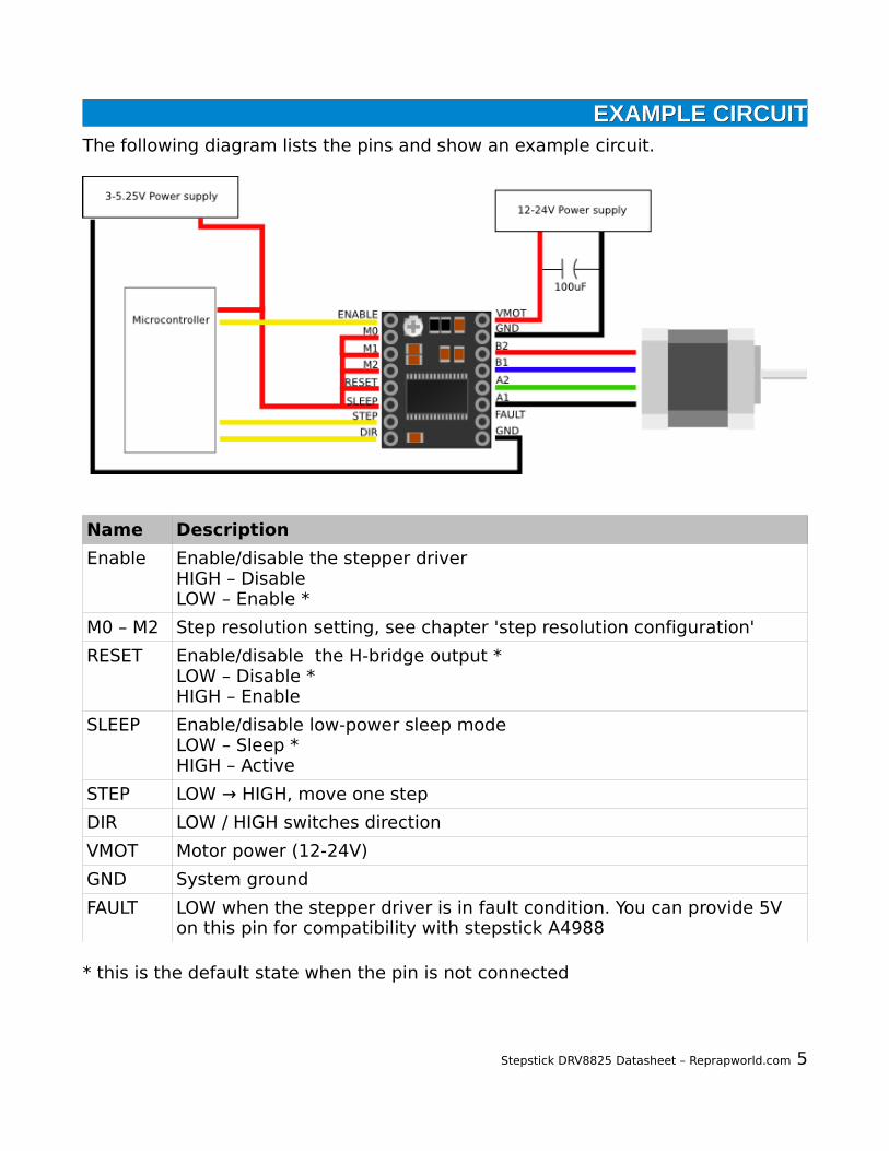
EXAMPLE CIRCUITEXAMPLE CIRCUITThe following diagram lists the pins and show an example circuit.
Name Description
Enable Enable/disable the stepper driverHIGH – DisableLOW – Enable *
M0 – M2 Step resolution setting, see chapter 'step resolution configuration'
RESET Enable/disable the H-bridge output *LOW – Disable *HIGH – Enable
SLEEP Enable/disable low-power sleep modeLOW – Sleep *HIGH – Active
STEP LOW → HIGH, move one step
DIR LOW / HIGH switches direction
VMOT Motor power (12-24V)
GND System ground
FAULT LOW when the stepper driver is in fault condition. You can provide 5V on this pin for compatibility with stepstick A4988
* this is the default state when the pin is not connected
Stepstick DRV8825 Datasheet – Reprapworld.com 5

STEP RESOLUTION CONFIGURATIONSTEP RESOLUTION CONFIGURATIONThe DRV8825 had six step resolution modes, which can be configured using the M0-M2 pins on the stepstick DRV8825. The following table lists the step resolution settings:
M0 M1 M2 ResolutionLow Low Low Full stepHigh Low Low Half stepLow High Low 1/4 stepHigh High Low 1/8 stepLow Low High 1/16 stepHigh Low High 1/32 stepLow High High 1/32 stepHigh High High 1/32 step
Stepstick DRV8825 Datasheet – Reprapworld.com 6

COMPATIBILITY WITH REPRAP HARDWARECOMPATIBILITY WITH REPRAP HARDWAREThe stepstick DRV8825 should be compatible with most RepRap hardware available. The following images show how to insert the stepstick DRV8825 in the most populair RepRap hardware.
Megatronics
The orientation of the stepstick is indicated with the trimpot, marked with a red circle.
Stepstick DRV8825 Datasheet – Reprapworld.com 7

RAMPS
The orientation of the stepstick is indicated with the trimpot, marked with a red circle.
Stepstick DRV8825 Datasheet – Reprapworld.com 8

TROUBLESHOOTINGTROUBLESHOOTING
The stepper motor doesold torque (you can rotate the stepper motor by hand)
- Check if the power is enabled- Is the ENABLE pin LOW?- Are SLEEP and RESET put HIGH?
The motor is losing steps while turning
- When the chip overheats the thermal protection will disable the device. Turn down the trimpot.- You may have not enough torque, turn the trimpot to the right to increase current.
Stepstick DRV8825 Datasheet – Reprapworld.com 9
02/26/09
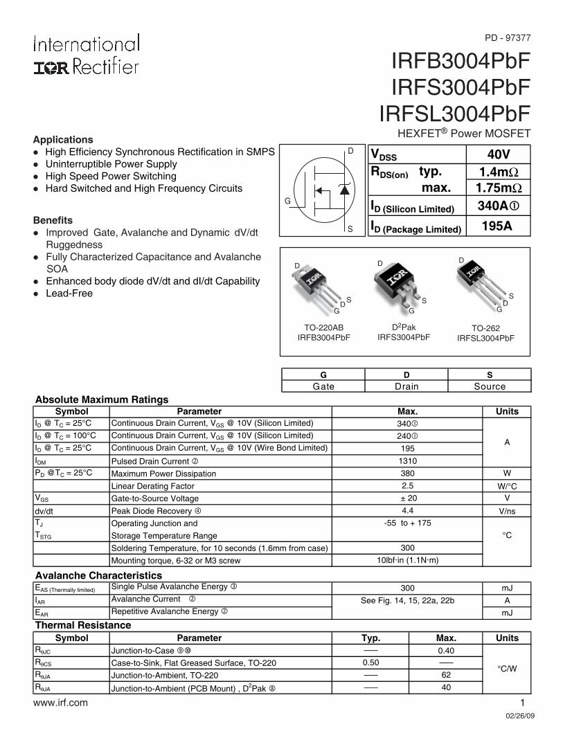
www.irf.com 1
HEXFETPower MOSFET
Benefits Improved Gate, Avalanche and Dynamic dV/dt
Ruggedness Fully Characterized Capacitance and Avalanche SOA Enhanced body diode dV/dt and dI/dt CapabilityLead-Free
ApplicationsHigh Efficiency Synchronous Rectification in SMPSUninterruptible Power SupplyHigh Speed Power SwitchingHard Switched and High Frequency Circuits
S
D
G
G D SGate Drain Source
IRFB3004PbFIRFS3004PbF
IRFSL3004PbF
D
SG
D2PakIRFS3004PbF
SD
G
D
TO-262IRFSL3004PbF
TO-220ABIRFB3004PbF
SD
G
D
Absolute Maximum RatingsSymbol Parameter Units
ID @ TC = 25°C Continuous Drain Current, VGS @ 10V (Silicon Limited)
ID @ TC = 100°C Continuous Drain Current, VGS @ 10V (Silicon Limited)
ID @ TC = 25°C Continuous Drain Current, VGS @ 10V (Wire Bond Limited)
IDM Pulsed Drain Current PD @TC = 25°C Maximum Power Dissipation W
Linear Derating Factor W/°CVGS Gate-to-Source Voltage V
dv/dt Peak Diode Recovery V/nsTJ Operating Junction andTSTG Storage Temperature Range
Soldering Temperature, for 10 seconds (1.6mm from case)
Mounting torque, 6-32 or M3 screw
Avalanche CharacteristicsEAS (Thermally limited) Single Pulse Avalanche Energy mJIAR Avalanche Current AEAR Repetitive Avalanche Energy mJ
Thermal ResistanceSymbol Parameter Typ. Max. Units
RθJC Junction-to-Case ––– 0.40RθCS Case-to-Sink, Flat Greased Surface, TO-220 0.50 –––RθJA Junction-to-Ambient, TO-220 ––– 62RθJA Junction-to-Ambient (PCB Mount) , D2Pak ––– 40
-55 to + 175
± 20
2.5
10lbfin (1.1Nm)
Max.340
240
1310
195
°C/W
A
°C
300
300
See Fig. 14, 15, 22a, 22b
380
4.4
VDSS 40VRDS(on) typ. 1.4mΩ max. 1.75mΩID (Silicon Limited) 340A
ID (Package Limited) 195A
2 www.irf.com
Calculated continuous current based on maximum allowable junction
temperature. Bond wire current limit is 195A. Note that currentlimitations arising from heating of the device leads may occur withsome lead mounting arrangements.
Repetitive rating; pulse width limited by max. junctiontemperature.
Limited by TJmax, starting TJ = 25°C, L = 0.016mH RG = 25Ω, IAS = 195A, VGS =10V. Part not recommended for use above this value .
S
D
G
ISD ≤ 195A, di/dt ≤ 930A/µs, VDD ≤ V(BR)DSS, TJ ≤ 175°C. Pulse width ≤ 400µs; duty cycle ≤ 2%. Coss eff. (TR) is a fixed capacitance that gives the same charging time as Coss while VDS is rising from 0 to 80% VDSS. Coss eff. (ER) is a fixed capacitance that gives the same energy as Coss while VDS is rising from 0 to 80% VDSS. When mounted on 1" square PCB (FR-4 or G-10 Material). For recom mended footprint and soldering techniques refer to application note #AN-994.θθJC !"#
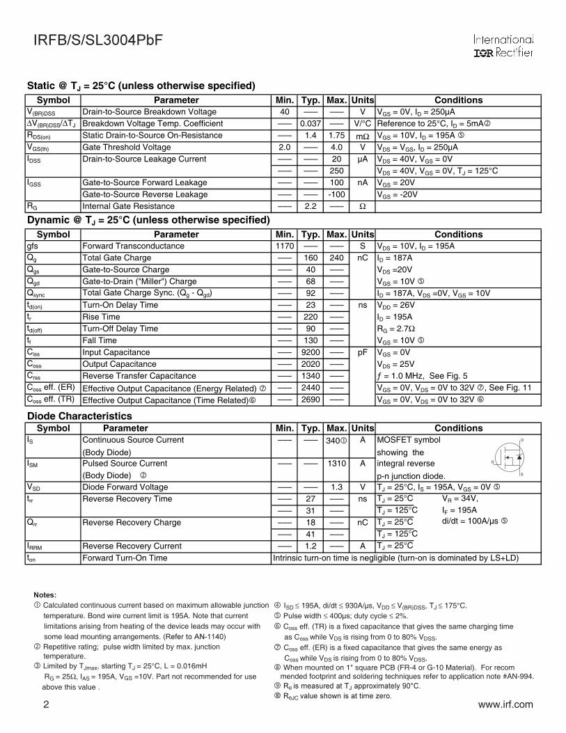
Static @ TJ = 25°C (unless otherwise specified)Symbol Parameter Min. Typ. Max. Units
V(BR)DSS Drain-to-Source Breakdown Voltage 40 ––– ––– V∆V(BR)DSS/∆TJ Breakdown Voltage Temp. Coefficient ––– 0.037 ––– V/°CRDS(on) Static Drain-to-Source On-Resistance ––– 1.4 1.75 mΩVGS(th) Gate Threshold Voltage 2.0 ––– 4.0 VIDSS Drain-to-Source Leakage Current ––– ––– 20 µA
––– ––– 250IGSS Gate-to-Source Forward Leakage ––– ––– 100 nA
Gate-to-Source Reverse Leakage ––– ––– -100RG Internal Gate Resistance ––– 2.2 ––– Ω
Dynamic @ TJ = 25°C (unless otherwise specified)Symbol Parameter Min. Typ. Max. Units
gfs Forward Transconductance 1170 ––– ––– SQg Total Gate Charge ––– 160 240 nCQgs Gate-to-Source Charge ––– 40 –––Qgd Gate-to-Drain ("Miller") Charge ––– 68 –––Qsync Total Gate Charge Sync. (Qg - Qgd) ––– 92 –––td(on) Turn-On Delay Time ––– 23 ––– nstr Rise Time ––– 220 –––td(off) Turn-Off Delay Time ––– 90 –––tf Fall Time ––– 130 –––Ciss Input Capacitance ––– 9200 ––– pFCoss Output Capacitance ––– 2020 –––Crss Reverse Transfer Capacitance ––– 1340 –––Coss eff. (ER) Effective Output Capacitance (Energy Related) ––– 2440 –––Coss eff. (TR) Effective Output Capacitance (Time Related) ––– 2690 –––
Diode CharacteristicsSymbol Parameter Min. Typ. Max. Units
IS Continuous Source Current ––– ––– 340 A
(Body Diode)ISM Pulsed Source Current ––– ––– 1310 A
(Body Diode)VSD Diode Forward Voltage ––– ––– 1.3 Vtrr Reverse Recovery Time ––– 27 ––– ns TJ = 25°C VR = 34V,
––– 31 ––– TJ = 125°C IF = 195AQrr Reverse Recovery Charge ––– 18 ––– nC TJ = 25°C di/dt = 100A/µs
––– 41 ––– TJ = 125°CIRRM Reverse Recovery Current ––– 1.2 ––– A TJ = 25°Cton Forward Turn-On Time Intrinsic turn-on time is negligible (turn-on is dominated by LS+LD)
ID = 195ARG = 2.7Ω
VGS = 10V
VDD = 26VID = 187A, VDS =0V, VGS = 10V
TJ = 25°C, IS = 195A, VGS = 0V
integral reverse
p-n junction diode.
ConditionsVGS = 0V, ID = 250µAReference to 25°C, ID = 5mAVGS = 10V, ID = 195A VDS = VGS, ID = 250µAVDS = 40V, VGS = 0VVDS = 40V, VGS = 0V, TJ = 125°C
MOSFET symbol
showing the
VDS =20V
Conditions
VGS = 10V VGS = 0VVDS = 25Vƒ = 1.0 MHz, See Fig. 5VGS = 0V, VDS = 0V to 32V , See Fig. 11VGS = 0V, VDS = 0V to 32V
ConditionsVDS = 10V, ID = 195AID = 187A
VGS = 20VVGS = -20V

www.irf.com 3
Fig 1. Typical Output Characteristics
Fig 3. Typical Transfer Characteristics Fig 4. Normalized On-Resistance vs. Temperature
Fig 2. Typical Output Characteristics
Fig 6. Typical Gate Charge vs. Gate-to-Source VoltageFig 5. Typical Capacitance vs. Drain-to-Source Voltage
0.1 1 10 100
VDS, Drain-to-Source Voltage (V)
10
100
1000
10000
I D, D
rain
-to-
Sou
rce
Cur
rent
(A
)
VGSTOP 15V
10V8.0V7.0V6.0V5.5V4.8V
BOTTOM 4.5V
≤60µs PULSE WIDTHTj = 25°C
4.5V
0.1 1 10 100
VDS, Drain-to-Source Voltage (V)
10
100
1000
10000
I D, D
rain
-to-
Sou
rce
Cur
rent
(A
)
4.5V
≤60µs PULSE WIDTHTj = 175°C
VGSTOP 15V
10V8.0V7.0V6.0V5.5V4.8V
BOTTOM 4.5V
1 2 3 4 5 6 7 8
VGS, Gate-to-Source Voltage (V)
0.1
1
10
100
1000
I D, D
rain
-to-
Sou
rce
Cur
rent
(A
)
TJ = 25°C
TJ = 175°C
VDS = 25V
≤60µs PULSE WIDTH
-60 -40 -20 0 20 40 60 80 100120140160180
TJ , Junction Temperature (°C)
0.5
1.0
1.5
2.0
RD
S(o
n) ,
Dra
in-t
o-S
ourc
e O
n R
esis
tanc
e
(
Nor
mal
ized
)
ID = 195A
VGS = 10V
1 10 100
VDS, Drain-to-Source Voltage (V)
100
1000
10000
100000
C, C
apac
itanc
e (p
F)
VGS = 0V, f = 1 MHZCiss = Cgs + Cgd, C ds SHORTED
Crss = Cgd Coss = Cds + Cgd
Coss
Crss
Ciss
0 50 100 150 200
QG, Total Gate Charge (nC)
0.0
2.0
4.0
6.0
8.0
10.0
12.0
14.0
VG
S, G
ate-
to-S
ourc
e V
olta
ge (
V)
VDS= 32V
VDS= 20V
ID= 187A

4 www.irf.com
Fig 8. Maximum Safe Operating Area
Fig 10. Drain-to-Source Breakdown Voltage
Fig 7. Typical Source-Drain DiodeForward Voltage
Fig 11. Typical COSS Stored Energy
Fig 9. Maximum Drain Current vs.Case Temperature
Fig 12. Maximum Avalanche Energy vs. DrainCurrent
0.0 0.5 1.0 1.5 2.0
VSD, Source-to-Drain Voltage (V)
0.1
1
10
100
1000
I SD
, Rev
erse
Dra
in C
urre
nt (
A)
TJ = 25°C
TJ = 175°C
VGS = 0V
-60 -40 -20 0 20 40 60 80 100120140160180
TJ , Temperature ( °C )
40
42
44
46
48
50
V(B
R)D
SS
, Dra
in-t
o-S
ourc
e B
reak
dow
n V
olta
ge (
V)
Id = 5mA
-5 0 5 10 15 20 25 30 35 40 45
VDS, Drain-to-Source Voltage (V)
0.0
0.2
0.4
0.6
0.8
1.0
1.2
1.4
1.6
1.8
2.0
Ene
rgy
(µJ)
25 50 75 100 125 150 175
Starting TJ , Junction Temperature (°C)
0
200
400
600
800
1000
1200
1400
EA
S ,
Sin
gle
Pul
se A
vala
nche
Ene
rgy
(mJ) ID
TOP 30A54A
BOTTOM 195A
25 50 75 100 125 150 175
TC , Case Temperature (°C)
0
50
100
150
200
250
300
350
I D,
Dra
in C
urre
nt (
A)
Limited By Package
1 10 100
VDS, Drain-to-Source Voltage (V)
1
10
100
1000
10000
I D,
Dra
in-t
o-S
ourc
e C
urre
nt (
A)
OPERATION IN THIS AREA LIMITED BY RDS(on)
Tc = 25°CTj = 175°CSingle Pulse
100µsec
1msec
10msec
DC

www.irf.com 5
Fig 13. Maximum Effective Transient Thermal Impedance, Junction-to-Case
Fig 14. Typical Avalanche Current vs.Pulsewidth
Fig 15. Maximum Avalanche Energy vs. Temperature
Notes on Repetitive Avalanche Curves , Figures 14, 15:(For further info, see AN-1005 at www.irf.com)1. Avalanche failures assumption:
Purely a thermal phenomenon and failure occurs at a temperature far inexcess of Tjmax. This is validated for every part type.
2. Safe operation in Avalanche is allowed as long asTjmax is not exceeded.3. Equation below based on circuit and waveforms shown in Figures 16a, 16b.4. PD (ave) = Average power dissipation per single avalanche pulse.5. BV = Rated breakdown voltage (1.3 factor accounts for voltage increase
during avalanche).6. Iav = Allowable avalanche current.7. ∆T = Allowable rise in junction temperature, not to exceed Tjmax (assumed as
25°C in Figure 14, 15).tav = Average time in avalanche.D = Duty cycle in avalanche = tav ·fZthJC(D, tav) = Transient thermal resistance, see Figures 13)
PD (ave) = 1/2 ( 1.3·BV·Iav) =T/ ZthJC
Iav = 2T/ [1.3·BV·Zth]EAS (AR) = PD (ave)·tav
1E-006 1E-005 0.0001 0.001 0.01 0.1
t1 , Rectangular Pulse Duration (sec)
0.001
0.01
0.1
1
The
rmal
Res
pons
e (
Z th
JC )
°C
/W
0.20
0.10
D = 0.50
0.020.01
0.05
SINGLE PULSE( THERMAL RESPONSE )
Notes:1. Duty Factor D = t1/t22. Peak Tj = P dm x Zthjc + Tc
τJ
τJ
τ1
τ1τ2
τ2 τ3
τ3
R1
R1 R2
R2 R3
R3
Ci i/RiCi= τi/Ri
ττC
τ4
τ4
R4
R4 Ri (°C/W) τi (sec)0.00646 0.000005
0.10020 0.000124
0.18747 0.001374
0.10667 0.008465
1.0E-06 1.0E-05 1.0E-04 1.0E-03 1.0E-02 1.0E-01
tav (sec)
1
10
100
1000
Ava
lanc
he C
urre
nt (
A)
0.05
Duty Cycle = Single Pulse
0.10
Allowed avalanche Current vs avalanche pulsewidth, tav, assuming ∆Τ j = 25°C and Tstart = 150°C.
0.01
Allowed avalanche Current vs avalanche pulsewidth, tav, assuming ∆Tj = 150°C and Tstart =25°C (Single Pulse)
25 50 75 100 125 150 175
Starting TJ , Junction Temperature (°C)
0
40
80
120
160
200
240
280
320
EA
R ,
Ava
lanc
he E
nerg
y (m
J)
TOP Single Pulse BOTTOM 1.0% Duty CycleID = 195A

6 www.irf.com
Fig 16. Threshold Voltage vs. Temperature
-75 -50 -25 0 25 50 75 100 125 150 175 200
TJ , Temperature ( °C )
1.0
1.5
2.0
2.5
3.0
3.5
4.0
4.5V
GS
(th)
, Gat
e th
resh
old
Vol
tage
(V
)
ID = 250µA
ID = 1.0mA
ID = 1.0A
100 200 300 400 500
diF /dt (A/µs)
50
100
150
200
250
300
350
QR
R (
nC)
IF = 78A
VR = 34V
TJ = 25°C
TJ = 125°C
100 200 300 400 500
diF /dt (A/µs)
0
50
100
150
200
250
300
350
400
QR
R (
nC)
IF = 117A
VR = 34V
TJ = 25°C
TJ = 125°C
100 200 300 400 500
diF /dt (A/µs)
2
3
4
5
6
7
8
9
10
I RR
M (
A)
IF = 78A
VR = 34V
TJ = 25°C
TJ = 125°C
100 200 300 400 500
diF /dt (A/µs)
1
2
3
4
5
6
7
8
9
10
11
I RR
M (
A)
IF = 117A
VR = 34V
TJ = 25°C
TJ = 125°C

www.irf.com 7
Fig 23a. Switching Time Test Circuit Fig 23b. Switching Time Waveforms
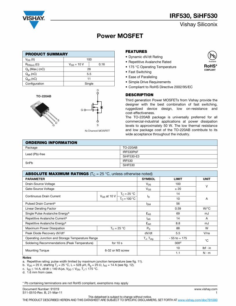
Fig 22b. Unclamped Inductive WaveformsFig 22a. Unclamped Inductive Test Circuit
tp
V(BR)DSS
IAS
RG
IAS
0.01Ωtp
D.U.T
LVDS
+- VDD
DRIVER
A
15V
20VVGS
Fig 24a. Gate Charge Test Circuit Fig 24b. Gate Charge Waveform
Vds
Vgs
Id
Vgs(th)
Qgs1 Qgs2 Qgd Qgodr
Fig 21. for N-ChannelHEXFETPower MOSFETs
• • •
P.W.Period
di/dt
Diode Recoverydv/dt
Ripple ≤ 5%
Body Diode Forward DropRe-AppliedVoltage
ReverseRecoveryCurrent
Body Diode ForwardCurrent
VGS=10V
VDD
ISD
Driver Gate Drive
D.U.T. ISD Waveform
D.U.T. VDS Waveform
Inductor Curent
D = P.W.Period
$%&$'()'*)
+
-
+
+
+-
-
-
$•
• !"#""• $%%• "#""&#
D.U.T.VDS
IDIG
3mA
VGS
.3µF
50KΩ
.2µF12V
Current RegulatorSame Type as D.U.T.
Current Sampling Resistors
+
-
VDS
90%
10%VGS
td(on) tr td(off) tf
$
'(≤ 1 )$≤ 0.1 %
$
*+
$
+-$
$

8 www.irf.com
Note: For the most current drawing please refer to IR website at http://www.irf.com/package/
!"##$%&''"()*+*$%", '$!$ %$%-$.&!"'#"&-/0""#
## 1
TO-220AB packages are not recommended for Surface Mount Application.

www.irf.com 9
TO-262 Part Marking Information
TO-262 Package OutlineDimensions are shown in millimeters (inches)
!
"
##

10 www.irf.com
!

www.irf.com 11
Data and specifications subject to change without notice. This product has been designed and qualified for the Industrial market.
Qualification Standards can be found on IR’s Web site.
IR WORLD HEADQUARTERS: 233 Kansas St., El Segundo, California 90245, USA Tel: (310) 252-7105TAC Fax: (310) 252-7903
Visit us at www.irf.com for sales contact information. 02/2009
!Dimensions are shown in millimeters (inches)
3
4
4
TRR
FEED DIRECTION
1.85 (.073)1.65 (.065)
1.60 (.063)1.50 (.059)
4.10 (.161)3.90 (.153)
TRL
FEED DIRECTION
10.90 (.429)10.70 (.421)
16.10 (.634)15.90 (.626)
1.75 (.069)1.25 (.049)
11.60 (.457)11.40 (.449)
15.42 (.609)15.22 (.601)
4.72 (.136)4.52 (.178)
24.30 (.957)23.90 (.941)
0.368 (.0145)0.342 (.0135)
1.60 (.063)1.50 (.059)
13.50 (.532)12.80 (.504)
330.00(14.173) MAX.
27.40 (1.079)23.90 (.941)
60.00 (2.362) MIN.
30.40 (1.197) MAX.
26.40 (1.039)24.40 (.961)
NOTES :1. COMFORMS TO EIA-418.2. CONTROLLING DIMENSION: MILLIMETER.3. DIMENSION MEASURED @ HUB.4. INCLUDES FLANGE DISTORTION @ OUTER EDGE.

November 2006 Rev 4 1/15
15
STP55NF06LSTB55NF06L - STB55NF06L-1
N-channel 60V - 0.014Ω - 55A TO-220/D2PAK/I2PAKSTripFET™ II Power MOSFET
General features
Exceptional dv/dt capability
100% avalanche tested
Application oriented characterization
DescriptionThis Power MOSFET is the latest development of STMicroelectronis unique "Single Feature Size™" strip-based process. The resulting transistor shows extremely high packing density for low on-resistance, rugged avalanche characteristics and less critical alignment steps therefore a remarkable manufacturing reproducibility.
Applications Switching application
Internal schematic diagram
Type VDSS RDS(on) ID
STP55NF06L 60V <0.018Ω 55A
STB55NF06L 60V <0.018Ω 55A
STB55NF06L-1 60V <0.018Ω 55A
TO-220
D2PAK I2PAK
13
1 2 3
12
3
www.st.com
Order codesPart number Marking Package Packaging
STP55NF06L P55NF06L TO-220 Tube
STB55NF06LT4 B55NF06L D2PAK Tape & reel
STB55NF06L-1 B55NF06L I2PAK Tube

Contents STB55NF06L - STB55NF06L-1 - STP55NF06L
2/15
Contents
1 Electrical ratings . . . . . . . . . . . . . . . . . . . . . . . . . . . . . . . . . . . . . . . . . . . . 3
2 Electrical characteristics . . . . . . . . . . . . . . . . . . . . . . . . . . . . . . . . . . . . . 4
2.1 Electrical characteristics (curves) . . . . . . . . . . . . . . . . . . . . . . . . . . . . 6
3 Test circuit . . . . . . . . . . . . . . . . . . . . . . . . . . . . . . . . . . . . . . . . . . . . . . . . 8
4 Package mechanical data . . . . . . . . . . . . . . . . . . . . . . . . . . . . . . . . . . . . . 9
5 Packaging mechanical data . . . . . . . . . . . . . . . . . . . . . . . . . . . . . . . . . . 13
6 Revision history . . . . . . . . . . . . . . . . . . . . . . . . . . . . . . . . . . . . . . . . . . . 14

STB55NF06L - STB55NF06L-1 - STP55NF06L Electrical ratings
3/15
1 Electrical ratings
Table 1. Absolute maximum ratings
Symbol Parameter Value Unit
VDS Drain-source voltage (VGS = 0) 60 V
VGS Gate-source voltage ± 16 V
ID Drain current (continuous) at TC = 25°C 55 A
ID Drain current (continuous) at TC = 100°C 39 A
IDM(1)
1. Pulse width limited by safe operating area
Drain current (pulsed) 220 A
PTOT Total dissipation at TC = 25°C 95 W
Derating factor 0.63 W/°C
dv/dt(2)
2. ISD ≤ 55A, di/dt ≤ 200A/µs, VDD ≤ V(BR)DSS, Tj ≤ TJMAX.
Peak diode recovery voltage slope 20 V/ns
EAS(3)
3. Starting Tj = 25 oC, ID = 27.5A, VDD= 30V.
Single pulse avalanche energy 300 mJ
TJ
Tstg
Operating junction temperature
Storage temperature-55 to 175 °C
Table 2. Thermal data
Rthj-case Thermal resistance junction-case max 1.58 °C/W
Rthj-a Thermal resistance junction-ambient max 62.5 °C/W
TlMaximum lead temperature for soldering purpose
300 °C

Electrical characteristics STB55NF06L - STB55NF06L-1 - STP55NF06L
4/15
2 Electrical characteristics
(TCASE=25°C unless otherwise specified)
Table 3. On/off states
Symbol Parameter Test conditions Min. Typ. Max. Unit
V(BR)DSSDrain-source breakdown voltage
ID = 250µA, VGS= 0 60 V
IDSSZero gate voltage drain current (VGS = 0)
VDS = Max rating,
VDS = Max rating @125°C
1
10
µA
µA
IGSSGate body leakage current
(VDS = 0)VGS = ±16V ±100 nA
VGS(th) Gate threshold voltage VDS= VGS, ID = 250µA 1 1.7 V
RDS(on)Static drain-source on resistance
VGS= 5V, ID= 27.5A
VGS= 10V, ID= 27.5A
0.016
0.014
0.020
0.018
ΩΩ
Table 4. Dynamic
Symbol Parameter Test conditions Min. Typ. Max. Unit
gfs (1)
1. Pulsed: pulse duration=300µs, duty cycle 1.5%
Forward transconductance VDS =15V, ID = 27.5A 30 S
Ciss
Coss
Crss
Input capacitanceOutput capacitance
Reverse transfer capacitance
VDS =25V, f=1 MHz, VGS=0
1700
300
105
pF
pF
pF
Qg
Qgs
Qgd
Total gate charge
Gate-source chargeGate-drain charge
VDD=48V, ID = 55A
VGS =4.5V
27
710
37 nC
nCnC

STB55NF06L - STB55NF06L-1 - STP55NF06L Electrical characteristics
5/15
Table 5. Switching times
Symbol Parameter Test conditions Min. Typ. Max. Unit
td(on)
tr
Turn-on delay time
Rise time
VDD=30 V, ID=27.5A,
RG=4.7Ω, VGS= 4.5V
(see Figure 12)
20
100
ns
ns
td(off)
tf
Turn-off delay timeFall time
VDD=30V, ID=27.5A,
RG=4.7Ω, VGS=4.5V
(see Figure 12)
4020
nsns
Table 6. Source drain diode
Symbol Parameter Test conditions Min Typ. Max Unit
ISD Source-drain current 12 A
ISDM(1)
1. Pulse width limited by safe operating area
Source-drain current (pulsed) 48 A
VSD(2)
2. Pulsed: pulse duration=300µs, duty cycle 1.5%
Forward on voltage ISD = 55A, VGS=0 1.6 V
trrQrr
IRRM
Reverse recovery time
Reverse recovery chargeReverse recovery current
ISD = 55A,
di/dt = 100A/µs,
VDD = 30V, Tj = 150°C
(see Figure 14)
80
2005
ns
nCA

Electrical characteristics STB55NF06L - STB55NF06L-1 - STP55NF06L
6/15
2.1 Electrical characteristics (curves) Figure 1. Safe operating area Figure 2. Thermal impedance
Figure 3. Output characterisics Figure 4. Transfer characteristics
Figure 5. Transconductance Figure 6. Static drain-source on resistance

STB55NF06L - STB55NF06L-1 - STP55NF06L Electrical characteristics
7/15
Figure 7. Gate charge vs gate-source voltage Figure 8. Capacitance variations
Figure 9. Normalized gate threshold voltage vs temperature
Figure 10. Normalized on resistance vs temperature
Figure 11. Source-drain diode forward characteristics

Test circuit STB55NF06L - STB55NF06L-1 - STP55NF06L
8/15
3 Test circuit
Figure 12. Switching times test circuit for resistive load
Figure 13. Gate charge test circuit
Figure 14. Test circuit for inductive load switching and diode recovery times
Figure 15. Unclamped Inductive load test circuit
Figure 16. Unclamped inductive waveform Figure 17. Switching time waveform

STB55NF06L - STB55NF06L-1 - STP55NF06L Package mechanical data
9/15
4 Package mechanical data
In order to meet environmental requirements, ST offers these devices in ECOPACK® packages. These packages have a Lead-free second level interconnect . The category of second level interconnect is marked on the package and on the inner box label, in compliance with JEDEC Standard JESD97. The maximum ratings related to soldering conditions are also marked on the inner box label. ECOPACK is an ST trademark. ECOPACK specifications are available at: www.st.com

Package mechanical data STB55NF06L - STB55NF06L-1 - STP55NF06L
10/15
TO-247 MECHANICAL DATA
1
DIM.mm. inch
MIN. TYP MAX. MIN. TYP. MAX.
A 4.4 4.6 0.173 0.181
A1 2.49 2.69 0.098 0.106
A2 0.03 0.23 0.001 0.009
B 0.7 0.93 0.027 0.036
B2 1.14 1.7 0.044 0.067
C 0.45 0.6 0.017 0.023
C2 1.23 1.36 0.048 0.053
D 8.95 9.35 0.352 0.368
D1 8 0.315
E 10 10.4 0.393
E1 8.5 0.334
G 4.88 5.28 0.192 0.208
L 15 15.85 0.590 0.625
L2 1.27 1.4 0.050 0.055
L3 1.4 1.75 0.055 0.068
M 2.4 3.2 0.094 0.126
R 0.4 0.015
V2 0º 4º
D2PAK MECHANICAL DATA
3

STB55NF06L - STB55NF06L-1 - STP55NF06L Package mechanical data
11/15
DIM.mm. inch
MIN. TYP MAX. MIN. TYP. MAX.
A 4.40 4.60 0.173 0.181
b 0.61 0.88 0.024 0.034
b1 1.15 1.70 0.045 0.066
c 0.49 0.70 0.019 0.027
D 15.25 15.75 0.60 0.620
E 10 10.40 0.393 0.409
e 2.40 2.70 0.094 0.106
e1 4.95 5.15 0.194 0.202
F 1.23 1.32 0.048 0.052
H1 6.20 6.60 0.244 0.256
J1 2.40 2.72 0.094 0.107
L 13 14 0.511 0.551
L1 3.50 3.93 0.137 0.154
L20 16.40 0.645
L30 28.90 1.137
øP 3.75 3.85 0.147 0.151
Q 2.65 2.95 0.104 0.116
TO-220 MECHANICAL DATA

Package mechanical data STB55NF06L - STB55NF06L-1 - STP55NF06L
12/15
DIM.mm. inch
MIN. TYP MAX. MIN. TYP. MAX.
A 4.40 4.60 0.173 0.181
A1 2.40 2.72 0.094 0.107
b 0.61 0.88 0.024 0.034
b1 1.14 1.70 0.044 0.066
c 0.49 0.70 0.019 0.027
c2 1.23 1.32 0.048 0.052
D 8.95 9.35 0.352 0.368
e 2.40 2.70 0.094 0.106
e1 4.95 5.15 0.194 0.202
E 10 10.40 0.393 0.410
L 13 14 0.511 0.551
L1 3.50 3.93 0.137 0.154
L2 1.27 1.40 0.050 0.055
TO-262 (I2PAK) MECHANICAL DATA

STB55NF06L - STB55NF06L-1 - STP55NF06L Packaging mechanical data
13/15
5 Packaging mechanical data
TAPE AND REEL SHIPMENT
D2PAK FOOTPRINT
* on sales type
DIM.mm inch
MIN. MAX. MIN. MAX.
A 330 12.992
B 1.5 0.059
C 12.8 13.2 0.504 0.520
D 20.2 0795
G 24.4 26.4 0.960 1.039
N 100 3.937
T 30.4 1.197
BASE QTY BULK QTY
1000 1000
REEL MECHANICAL DATA
DIM.mm inch
MIN. MAX. MIN. MAX.
A0 10.5 10.7 0.413 0.421
B0 15.7 15.9 0.618 0.626
D 1.5 1.6 0.059 0.063
D1 1.59 1.61 0.062 0.063
E 1.65 1.85 0.065 0.073
F 11.4 11.6 0.449 0.456
K0 4.8 5.0 0.189 0.197
P0 3.9 4.1 0.153 0.161
P1 11.9 12.1 0.468 0.476
P2 1.9 2.1 0.075 0.082
R 50 1.574
T 0.25 0.35 0.0098 0.0137
W 23.7 24.3 0.933 0.956
TAPE MECHANICAL DATA

Revision history STB55NF06L - STB55NF06L-1 - STP55NF06L
14/15
6 Revision history
Table 7. Revision history
Date Revision Changes
09-Sep-2004 3 Complete document
27-Nov-2006 4 The document has been reformatted

STB55NF06L - STB55NF06L-1 - STP55NF06L
15/15
Please Read Carefully:
Information in this document is provided solely in connection with ST products. STMicroelectronics NV and its subsidiaries (“ST”) reserve theright to make changes, corrections, modifications or improvements, to this document, and the products and services described herein at anytime, without notice.
All ST products are sold pursuant to ST’s terms and conditions of sale.
Purchasers are solely responsible for the choice, selection and use of the ST products and services described herein, and ST assumes noliability whatsoever relating to the choice, selection or use of the ST products and services described herein.
No license, express or implied, by estoppel or otherwise, to any intellectual property rights is granted under this document. If any part of thisdocument refers to any third party products or services it shall not be deemed a license grant by ST for the use of such third party productsor services, or any intellectual property contained therein or considered as a warranty covering the use in any manner whatsoever of suchthird party products or services or any intellectual property contained therein.
UNLESS OTHERWISE SET FORTH IN ST’S TERMS AND CONDITIONS OF SALE ST DISCLAIMS ANY EXPRESS OR IMPLIEDWARRANTY WITH RESPECT TO THE USE AND/OR SALE OF ST PRODUCTS INCLUDING WITHOUT LIMITATION IMPLIEDWARRANTIES OF MERCHANTABILITY, FITNESS FOR A PARTICULAR PURPOSE (AND THEIR EQUIVALENTS UNDER THE LAWSOF ANY JURISDICTION), OR INFRINGEMENT OF ANY PATENT, COPYRIGHT OR OTHER INTELLECTUAL PROPERTY RIGHT.
UNLESS EXPRESSLY APPROVED IN WRITING BY AN AUTHORIZED ST REPRESENTATIVE, ST PRODUCTS ARE NOTRECOMMENDED, AUTHORIZED OR WARRANTED FOR USE IN MILITARY, AIR CRAFT, SPACE, LIFE SAVING, OR LIFE SUSTAININGAPPLICATIONS, NOR IN PRODUCTS OR SYSTEMS WHERE FAILURE OR MALFUNCTION MAY RESULT IN PERSONAL INJURY,DEATH, OR SEVERE PROPERTY OR ENVIRONMENTAL DAMAGE. ST PRODUCTS WHICH ARE NOT SPECIFIED AS "AUTOMOTIVEGRADE" MAY ONLY BE USED IN AUTOMOTIVE APPLICATIONS AT USER’S OWN RISK.
Resale of ST products with provisions different from the statements and/or technical features set forth in this document shall immediately voidany warranty granted by ST for the ST product or service described herein and shall not create or extend in any manner whatsoever, anyliability of ST.
ST and the ST logo are trademarks or registered trademarks of ST in various countries.
Information in this document supersedes and replaces all information previously supplied.
The ST logo is a registered trademark of STMicroelectronics. All other names are the property of their respective owners.
© 2006 STMicroelectronics - All rights reserved
STMicroelectronics group of companies
Australia - Belgium - Brazil - Canada - China - Czech Republic - Finland - France - Germany - Hong Kong - India - Israel - Italy - Japan - Malaysia - Malta - Morocco - Singapore - Spain - Sweden - Switzerland - United Kingdom - United States of America
www.st.com
Document Number: 91019 www.vishay.comS11-0510-Rev. B, 21-Mar-11 1
This datasheet is subject to change without notice.THE PRODUCT DESCRIBED HEREIN AND THIS DATASHEET ARE SUBJECT TO SPECIFIC DISCLAIMERS, SET FORTH AT www.vishay.com/doc?91000
Power MOSFET
IRF530, SiHF530Vishay Siliconix
FEATURES• Dynamic dV/dt Rating• Repetitive Avalanche Rated• 175 °C Operating Temperature• Fast Switching• Ease of Paralleling• Simple Drive Requirements• Compliant to RoHS Directive 2002/95/EC
DESCRIPTIONThird generation Power MOSFETs from Vishay provide thedesigner with the best combination of fast switching,ruggedized device design, low on-resistance andcost-effectiveness. The TO-220AB package is universally preferred for allcommercial-industrial applications at power dissipationlevels to approximately 50 W. The low thermal resistanceand low package cost of the TO-220AB contribute to itswide acceptance throughout the industry.
Notesa. Repetitive rating; pulse width limited by maximum junction temperature (see fig. 11).b. VDD = 25 V, starting TJ = 25 °C, L = 528 μH, Rg = 25 , IAS = 14 A (see fig. 12).c. ISD 14 A, dI/dt 140 A/μs, VDD VDS, TJ 175 °C.d. 1.6 mm from case.
PRODUCT SUMMARYVDS (V) 100
RDS(on) () VGS = 10 V 0.16
Qg (Max.) (nC) 26
Qgs (nC) 5.5
Qgd (nC) 11
Configuration Single
N-Channel MOSFET
G
D
S
TO-220AB
GDS
Available
RoHS*COMPLIANT
ORDERING INFORMATIONPackage TO-220AB
Lead (Pb)-freeIRF530PbFSiHF530-E3
SnPbIRF530SiHF530
ABSOLUTE MAXIMUM RATINGS (TC = 25 °C, unless otherwise noted)PARAMETER SYMBOL LIMIT UNIT
Drain-Source Voltage VDS 100V
Gate-Source Voltage VGS ± 20
Continuous Drain Current VGS at 10 VTC = 25 °C
ID14
ATC = 100 °C 10
Pulsed Drain Currenta IDM 56
Linear Derating Factor 0.59 W/°C
Single Pulse Avalanche Energyb EAS 69 mJ
Repetitive Avalanche Currenta IAR 14 A
Repetitive Avalanche Energya EAR 8.8 mJ
Maximum Power Dissipation TC = 25 °C PD 88 W
Peak Diode Recovery dV/dtc dV/dt 5.5 V/ns
Operating Junction and Storage Temperature Range TJ, Tstg - 55 to + 175 °C
Soldering Recommendations (Peak Temperature) for 10 s 300d
Mounting Torque 6-32 or M3 screw10 lbf · in
1.1 N · m
* Pb containing terminations are not RoHS compliant, exemptions may apply

www.vishay.com Document Number: 910192 S11-0510-Rev. B, 21-Mar-11
This datasheet is subject to change without notice.THE PRODUCT DESCRIBED HEREIN AND THIS DATASHEET ARE SUBJECT TO SPECIFIC DISCLAIMERS, SET FORTH AT www.vishay.com/doc?91000
IRF530, SiHF530Vishay Siliconix
Notesa. Repetitive rating; pulse width limited by maximum junction temperature (see fig. 11).b. Pulse width 300 μs; duty cycle 2 %.
THERMAL RESISTANCE RATINGSPARAMETER SYMBOL TYP. MAX. UNIT
Maximum Junction-to-Ambient RthJA - 62
°C/WCase-to-Sink, Flat, Greased Surface RthCS 0.50 -
Maximum Junction-to-Case (Drain) RthJC - 1.7
SPECIFICATIONS (TJ = 25 °C, unless otherwise noted)PARAMETER SYMBOL TEST CONDITIONS MIN. TYP. MAX. UNIT
Static
Drain-Source Breakdown Voltage VDS VGS = 0 V, ID = 250 μA 100 - - V
VDS Temperature Coefficient VDS/TJ Reference to 25 °C, ID = 1 mA - 0.12 - V/°C
Gate-Source Threshold Voltage VGS(th) VDS = VGS, ID = 250 μA 2.0 - 4.0 V
Gate-Source Leakage IGSS VGS = ± 20 V - - ± 100 nA
Zero Gate Voltage Drain Current IDSS VDS = 100 V, VGS = 0 V - - 25
μA VDS = 80 V, VGS = 0 V, TJ = 150 °C - - 250
Drain-Source On-State Resistance RDS(on) VGS = 10 V ID = 8.4 Ab - - 0.16
Forward Transconductance gfs VDS = 50 V, ID = 8.4 Ab 5.1 - - S
Dynamic
Input Capacitance Ciss VGS = 0 V,
VDS = 25 V,
f = 1.0 MHz, see fig. 5
- 670 -
pFOutput Capacitance Coss - 250 -
Reverse Transfer Capacitance Crss - 60 -
Total Gate Charge Qg
VGS = 10 V ID = 14 A, VDS = 80 V,
see fig. 6 and 13b
- - 26
nC Gate-Source Charge Qgs - - 5.5
Gate-Drain Charge Qgd - - 11
Turn-On Delay Time td(on)
VDD = 50 V, ID = 14 A Rg = 12 , RD = 3.6, see fig. 10b
- 10 -
nsRise Time tr - 34 -
Turn-Off Delay Time td(off) - 23 -
Fall Time tf - 24 -
Internal Drain Inductance LD Between lead,6 mm (0.25") from package and center of die contact
- 4.5 -
nH
Internal Source Inductance LS - 7.5 -
Drain-Source Body Diode Characteristics
Continuous Source-Drain Diode Current ISMOSFET symbol
showing the integral reversep - n junction diode
- - 14
APulsed Diode Forward Currenta ISM - - 56
Body Diode Voltage VSD TJ = 25 °C, IS = 14 A, VGS = 0 Vb - - 2.5 V
Body Diode Reverse Recovery Time trrTJ = 25 °C, IF = 14 A, dI/dt = 100 A/μsb
- 150 280 ns
Body Diode Reverse Recovery Charge Qrr - 0.85 1.7 μC
Forward Turn-On Time ton Intrinsic turn-on time is negligible (turn-on is dominated by LS and LD)
D
S
G
S
D
G

Document Number: 91019 www.vishay.comS11-0510-Rev. B, 21-Mar-11 3
This datasheet is subject to change without notice.THE PRODUCT DESCRIBED HEREIN AND THIS DATASHEET ARE SUBJECT TO SPECIFIC DISCLAIMERS, SET FORTH AT www.vishay.com/doc?91000
IRF530, SiHF530 Vishay Siliconix
TYPICAL CHARACTERISTICS (25 °C, unless otherwise noted)
Fig. 1 - Typical Output Characteristics, TC = 25 °C
Fig. 2 - Typical Output Characteristics, TC = 175 °C
Fig. 3 - Typical Transfer Characteristics
Fig. 4 - Normalized On-Resistance vs. Temperature
91019_01
20 µs Pulse WidthTC = 25 °C
4.5 V
VDS, Drain-to-Source Voltage (V)
I D, D
rain
Cur
rent
(A
)
Bottom
TopVGS
15 V10 V8.0 V7.0 V6.0 V5.5 V5.0 V4.5 V
101
100
10-1 100 101
VDS, Drain-to-Source Voltage (V)
I D, D
rain
Cur
rent
(A
)
4.5 V
20 µs Pulse WidthTC = 175 °C
91019_02
Bottom
TopVGS
15 V10 V8.0 V7.0 V6.0 V5.5 V5.0 V4.5 V
101
100
10-1 100 101
20 µs Pulse WidthVDS = 50 V
I D, D
rain
Cur
rent
(A
)
VGS, Gate-to-Source Voltage (V)
5 6 7 8 9 104
25 °C
175 °C
91019_03
101
100
ID = 14 AVGS = 10 V
3.0
0.0
0.5
1.0
1.5
2.0
2.5
- 60- 40 - 20 0 20 40 60 80 100120 140 160
TJ, Junction Temperature (°C)
RD
S(o
n), D
rain
-to-
Sou
rce
On
Res
ista
nce
(Nor
mal
ized
)
91019_04
3.5
180

www.vishay.com Document Number: 910194 S11-0510-Rev. B, 21-Mar-11
This datasheet is subject to change without notice.THE PRODUCT DESCRIBED HEREIN AND THIS DATASHEET ARE SUBJECT TO SPECIFIC DISCLAIMERS, SET FORTH AT www.vishay.com/doc?91000
IRF530, SiHF530Vishay Siliconix
Fig. 5 - Typical Capacitance vs. Drain-to-Source Voltage
Fig. 6 - Typical Gate Charge vs. Gate-to-Source Voltage
Fig. 7 - Typical Source-Drain Diode Forward Voltage
Fig. 8 - Maximum Safe Operating Area
1400
1200
1000
800
0
400
600
100 101
Cap
acita
nce
(pF
)
VDS, Drain-to-Source Voltage (V)
Ciss
Crss
Coss
VGS = 0 V, f = 1 MHzCiss = Cgs + Cgd, Cds ShortedCrss = CgdCoss = Cds + Cgd
91019_05
200
QG, Total Gate Charge (nC)
VG
S, G
ate-
to-S
ourc
e V
olta
ge (
V)
20
16
12
8
0
4
0 5 25201510
ID = 14 A
VDS = 20 V
VDS = 50 V
For test circuitsee figure 13
VDS = 80 V
91019_06
101
100
VSD, Source-to-Drain Voltage (V)
I SD, R
ever
se D
rain
Cur
rent
(A
)
0.4 2.01.61.20.8
25 °C
175 °C
VGS = 0 V
91019_07
102
10 µs
100 µs
1 ms
10 ms
Operation in this area limitedby RDS(on)
VDS, Drain-to-Source Voltage (V)
I D, D
rain
Cur
rent
(A
)
TC = 25 °CTJ = 175 °CSingle Pulse
0.1
103
0.1
2
5
1
2
5
10
2
5
2
5
2 51
2 510 2 5 102 2 5
103
91019_08

Document Number: 91019 www.vishay.comS11-0510-Rev. B, 21-Mar-11 5
This datasheet is subject to change without notice.THE PRODUCT DESCRIBED HEREIN AND THIS DATASHEET ARE SUBJECT TO SPECIFIC DISCLAIMERS, SET FORTH AT www.vishay.com/doc?91000
IRF530, SiHF530 Vishay Siliconix
Fig. 9 - Maximum Drain Current vs. Case Temperature
Fig. 10a - Switching Time Test Circuit
Fig. 10b - Switching Time Waveforms
Fig. 11 - Maximum Effective Transient Thermal Impedance, Junction-to-Case
I D, D
rain
Cur
rent
(A
)
TC, Case Temperature (°C)
0
6
8
10
12
14
25 1501251007550
91019_09
4
2
175
Pulse width ≤ 1 µsDuty factor ≤ 0.1 %
RD
VGS
RG
D.U.T.
10 V
+-
VDS
VDD
VDS
90 %
10 %VGS
td(on) tr td(off) tf
10
1
0.1
10-2
10-5 10-4 10-3 10-2 0.1 1 10
PDM
t1t2
t1, Rectangular Pulse Duration (s)
The
rmal
Res
pons
e (Z
thJC
)
Notes:1. Duty Factor, D = t1/t22. Peak Tj = PDM x ZthJC + TC
Single Pulse(Thermal Response)
0 - 0.5
0.2
0.1
0.05
0.020.01
91019_11
www.vishay.com Document Number: 910196 S11-0510-Rev. B, 21-Mar-11
This datasheet is subject to change without notice.THE PRODUCT DESCRIBED HEREIN AND THIS DATASHEET ARE SUBJECT TO SPECIFIC DISCLAIMERS, SET FORTH AT www.vishay.com/doc?91000
IRF530, SiHF530Vishay Siliconix
Fig. 12a - Unclamped Inductive Test Circuit Fig. 12b - Unclamped Inductive Waveforms
Fig. 12c - Maximum Avalanche Energy vs. Drain Current
Fig. 13a - Basic Gate Charge Waveform Fig. 13b - Gate Charge Test Circuit
RG
IAS
0.01 Ωtp
D.U.T
LVDS
+
-VDD
10 V
Vary tp to obtainrequired IAS
IAS
VDS
VDD
VDS
tp
200
0
40
80
120
160
25 1501251007550
Starting TJ, Junction Temperature (°C)
EA
S, S
ingl
e P
ulse
Ene
rgy
(mJ)
Bottom
TopID
5.7 A9.9 A14 A
VDD = 25 V
91019_12c
175
QGS QGD
QG
VG
Charge
10 V
D.U.T.
3 mA
VGS
VDS
IG ID
0.3 µF0.2 µF
50 kΩ
12 V
Current regulator
Current sampling resistors
Same type as D.U.T.
+
-

Document Number: 91019 www.vishay.comS11-0510-Rev. B, 21-Mar-11 7
This datasheet is subject to change without notice.THE PRODUCT DESCRIBED HEREIN AND THIS DATASHEET ARE SUBJECT TO SPECIFIC DISCLAIMERS, SET FORTH AT www.vishay.com/doc?91000
IRF530, SiHF530 Vishay Siliconix
Fig. 14 - For N-Channel
Vishay Siliconix maintains worldwide manufacturing capability. Products may be manufactured at one of several qualified locations. Reliability data for SiliconTechnology and Package Reliability represent a composite of all qualified locations. For related documents such as package/tape drawings, part marking, andreliability data, see www.vishay.com/ppg?91019.
P.W.Period
dI/dt
Diode recoverydV/dt
Ripple ≤ 5 %
Body diode forward drop
Re-appliedvoltage
Reverserecoverycurrent
Body diode forwardcurrent
VGS = 10 Va
ISD
Driver gate drive
D.U.T. lSD waveform
D.U.T. VDS waveform
Inductor current
D = P.W.Period
+
-
+
+
+-
-
-
Peak Diode Recovery dV/dt Test Circuit
VDD
• dV/dt controlled by Rg
• Driver same type as D.U.T.• ISD controlled by duty factor “D”• D.U.T. - device under test
D.U.T.Circuit layout considerations
• Low stray inductance• Ground plane• Low leakage inductance
current transformer
Rg
Notea. VGS = 5 V for logic level devices
VDD
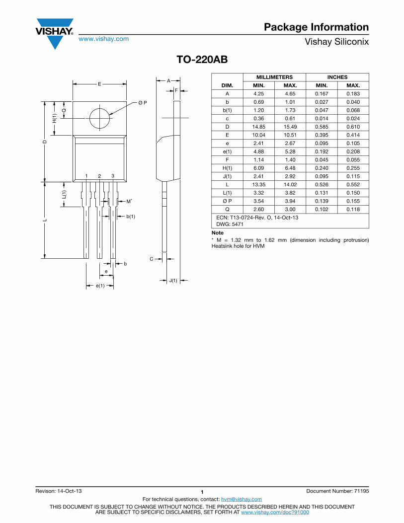
Package Informationwww.vishay.com Vishay Siliconix
Revison: 14-Oct-13 1 Document Number: 71195
For technical questions, contact: [email protected] DOCUMENT IS SUBJECT TO CHANGE WITHOUT NOTICE. THE PRODUCTS DESCRIBED HEREIN AND THIS DOCUMENT
ARE SUBJECT TO SPECIFIC DISCLAIMERS, SET FORTH AT www.vishay.com/doc?91000
TO-220AB
Note* M = 1.32 mm to 1.62 mm (dimension including protrusion)Heatsink hole for HVM
M*
321
L
L(1)
D
H(1
)
Q
Ø P
A
F
J(1)
b(1)
e(1)
e
E
bC
MILLIMETERS INCHES
DIM. MIN. MAX. MIN. MAX.
A 4.25 4.65 0.167 0.183
b 0.69 1.01 0.027 0.040
b(1) 1.20 1.73 0.047 0.068
c 0.36 0.61 0.014 0.024
D 14.85 15.49 0.585 0.610
E 10.04 10.51 0.395 0.414
e 2.41 2.67 0.095 0.105
e(1) 4.88 5.28 0.192 0.208
F 1.14 1.40 0.045 0.055
H(1) 6.09 6.48 0.240 0.255
J(1) 2.41 2.92 0.095 0.115
L 13.35 14.02 0.526 0.552
L(1) 3.32 3.82 0.131 0.150
Ø P 3.54 3.94 0.139 0.155
Q 2.60 3.00 0.102 0.118
ECN: T13-0724-Rev. O, 14-Oct-13DWG: 5471

Legal Disclaimer Noticewww.vishay.com Vishay
Revision: 02-Oct-12 1 Document Number: 91000
DisclaimerALL PRODUCT, PRODUCT SPECIFICATIONS AND DATA ARE SUBJECT TO CHANGE WITHOUT NOTICE TO IMPROVERELIABILITY, FUNCTION OR DESIGN OR OTHERWISE.
Vishay Intertechnology, Inc., its affiliates, agents, and employees, and all persons acting on its or their behalf (collectively,“Vishay”), disclaim any and all liability for any errors, inaccuracies or incompleteness contained in any datasheet or in any otherdisclosure relating to any product.
Vishay makes no warranty, representation or guarantee regarding the suitability of the products for any particular purpose orthe continuing production of any product. To the maximum extent permitted by applicable law, Vishay disclaims (i) any and allliability arising out of the application or use of any product, (ii) any and all liability, including without limitation special,consequential or incidental damages, and (iii) any and all implied warranties, including warranties of fitness for particularpurpose, non-infringement and merchantability.
Statements regarding the suitability of products for certain types of applications are based on Vishay’s knowledge of typicalrequirements that are often placed on Vishay products in generic applications. Such statements are not binding statementsabout the suitability of products for a particular application. It is the customer’s responsibility to validate that a particularproduct with the properties described in the product specification is suitable for use in a particular application. Parametersprovided in datasheets and/or specifications may vary in different applications and performance may vary over time. Alloperating parameters, including typical parameters, must be validated for each customer application by the customer’stechnical experts. Product specifications do not expand or otherwise modify Vishay’s terms and conditions of purchase,including but not limited to the warranty expressed therein.
Except as expressly indicated in writing, Vishay products are not designed for use in medical, life-saving, or life-sustainingapplications or for any other application in which the failure of the Vishay product could result in personal injury or death.Customers using or selling Vishay products not expressly indicated for use in such applications do so at their own risk. Pleasecontact authorized Vishay personnel to obtain written terms and conditions regarding products designed for such applications.
No license, express or implied, by estoppel or otherwise, to any intellectual property rights is granted by this document or byany conduct of Vishay. Product names and markings noted herein may be trademarks of their respective owners.
Material Category PolicyVishay Intertechnology, Inc. hereby certifies that all its products that are identified as RoHS-Compliant fulfill thedefinitions and restrictions defined under Directive 2011/65/EU of The European Parliament and of the Councilof June 8, 2011 on the restriction of the use of certain hazardous substances in electrical and electronic equipment(EEE) - recast, unless otherwise specified as non-compliant.
Please note that some Vishay documentation may still make reference to RoHS Directive 2002/95/EC. We confirm thatall the products identified as being compliant to Directive 2002/95/EC conform to Directive 2011/65/EU.
Vishay Intertechnology, Inc. hereby certifies that all its products that are identified as Halogen-Free follow Halogen-Freerequirements as per JEDEC JS709A standards. Please note that some Vishay documentation may still make referenceto the IEC 61249-2-21 definition. We confirm that all the products identified as being compliant to IEC 61249-2-21conform to JEDEC JS709A standards.

!
"#
! !
$%
&'
( ) (*& ))+'
, - )& ).+'/
. 0-
* -#1
$ %00,)2!3 %-.
4$567,8 .

9/" :
6 ))
;7
&8)67<) '()
7;7 ,)
60;*) ) . 8
"= * =
5" **>))
" **>))
0
? @& )@,+';4A(@)-*
$ %00,)2!3 %(-.
4$567,8 .

!
# 9 9/ : 7
0 B @) C)
$<.
= ( .) $(&; @'
3 *@* 9
D&; '
6 *@B $,
0- ,)
;= = ( ( @ = C()
"7 )) =C*=
7 7 ,* ; =C)<-C9E
$% 0-#/73
&760F3'
( --/-/
, <-73
--
. #*G
$ %00,)2!3 %,-.
4$567,8 .

" ! #
&(* #:5$'
$ %00,)2!3 %.-.

Mouser Electronics
Authorized Distributor
Click to View Pricing, Inventory, Delivery & Lifecycle Information: Lite-On:
LTL-307GE

NTC thermistors for
temperature measurement
Glass-encapsulated sensors,standard type
Series/Type: B57560G, B57560G1
Date: February 2009
© EPCOS AG 2009. Reproduction, publication and dissemination of this publication, enclosures hereto and theinformation contained therein without EPCOS' prior express consent is prohibited.
The following products presented in this data sheet are being withdrawn.
Ordering Code Substitute Product Date ofWithdrawal
Deadline LastOrders
Last Shipments
B57560G0145* B57560G1104* 2012-03-23 2012-06-28 2012-09-28
For further information please contact your nearest EPCOS sales office, which will also supportyou in selecting a suitable substitute. The addresses of our worldwide sales network arepresented at www.epcos.com/sales.

Applications
Temperature measurement
Features
Glass-encapsulated, heat-resistive andhighly stableFor temperature measurement up to300 °CLeads: dumet wires (copper-clad FeNi)
Options
Leads: nickel-plated dumet wiresAlternative dimensions available on request
Delivery mode
Bulk
Dimensional drawing
Dimensions in mm
General technical data
Climatic category (IEC 60068-1) 55/300/56Max. power (at 25 °C) P25 50 mWResistance tolerance ∆RR/RR ±1, ±2, ±3 %Rated temperature TR 25 °CDissipation factor (in air) δth approx. 1.3 mW/KThermal cooling time constant (in air) τc approx. 15 sHeat capacity Cth approx. 20 mJ/K
Temperature measurement B57560G, B57560G1
Glass-encapsulated sensors G560/G1560
Page 2 of 18Please read Cautions and warnings andImportant notes at the end of this document.

1) B200/300
Electrical specification and ordering codes
R25
ΩNo. of R/Tcharacteristic
B25/85
KB0/100
KB25/100
KOrdering code
+ = Resistance toleranceF = ±1%G = ±2%H = ±3%
The last three digits of the ordering code denote:000 and 005 = dumet wires002 and 007 = nickel-plated wires
2 k 8401 3420 3390 ±1% 3436 B57560G0202+0002 k 8401 3420 3390 ±1% 3436 B57560G0202+0025 k 8402 3480 3450 ±1% 3497 B57560G0502+0005 k 8402 3480 3450 ±1% 3497 B57560G0502+002
10 k 7003 3612 3586 3625 ±1% B57560G1103+00510 k 7003 3612 3586 3625 ±1% B57560G1103+00710 k 8307 3478 3450 3492 ±1% B57560G1103+00010 k 8307 3478 3450 3492 ±1% B57560G1103+00220 k 8415 3992 3970 ±1% 4006 B57560G0203+00020 k 8415 3992 3970 ±1% 4006 B57560G0203+00230 k 7002 3973 3944 3988 ±1% B57560G1303+00530 k 7002 3973 3944 3988 ±1% B57560G1303+00750 k 8403 3992 3970 ±1% 4006 B57560G0503+00050 k 8403 3992 3970 ±1% 4006 B57560G0503+002
100 k 8304 4072 4036 4092 ±1% B57560G1104+000100 k 8304 4072 4036 4092 ±1% B57560G1104+002
1400 k 8406 4557 5133 ±2%1) 4581 B57560G0145+0001400 k 8406 4557 5133 ±2%1) 4581 B57560G0145+002
Temperature measurement B57560G, B57560G1
Glass-encapsulated sensors G560/G1560
Page 3 of 18Please read Cautions and warnings andImportant notes at the end of this document.

Reliability data
Test Standard Test conditions ∆R25/R25
(typical)Remarks
Storage indry heat
IEC60068-2-2
Storage at uppercategory temperatureT: 300 °Ct: 1000 h
< 3% No visibledamage
Storage in dampheat, steady state
IEC60068-2-67
Temperature of air: 85 °CRelative humidity of air: 85%Duration: 56 days
< 2% No visibledamage
Rapid temperaturecycling
IEC60068-2-14
Lower test temperature: 55 °CUpper test temperature: 200 °CNumber of cycles: 1000
< 2% No visibledamage
Temperature measurement B57560G, B57560G1
Glass-encapsulated sensors G560/G1560
Page 4 of 18Please read Cautions and warnings andImportant notes at the end of this document.

R/T characteristics
R/T No. 7002 7003 8304
T (°C) B25/100 = 3988 K B25/100 = 3625 K B25/100 = 4092 KRT/R25 α (%/K) RT/R25 α (%/K) RT/R25 α (%/K)
55.0 96.33 7.4 63.225 6.7 100.11 7.450.0 66.866 7.2 45.46 6.5 69.56 7.245.0 47.037 6.9 33.07 6.3 48.945 6.940.0 33.508 6.7 24.324 6.0 34.853 6.735.0 24.156 6.4 18.081 5.8 25.102 6.530.0 17.613 6.2 13.575 5.6 18.275 6.225.0 12.98 6.0 10.29 5.4 13.443 6.020.0 9.6643 5.8 7.8716 5.3 9.9853 5.915.0 7.2656 5.6 6.0739 5.1 7.4867 5.710.0 5.5129 5.4 4.7258 4.9 5.6636 5.55.0 4.22 5.3 3.7062 4.8 4.3212 5.30.0 3.2575 5.1 2.9287 4.6 3.324 5.25.0 2.5348 4.9 2.3311 4.5 2.5769 5.0
10.0 1.9876 4.8 1.8684 4.4 2.0127 4.915.0 1.5699 4.6 1.5075 4.2 1.5834 4.720.0 1.2488 4.5 1.224 4.1 1.2542 4.625.0 1.0000 4.4 1.0000 4.0 1.0000 4.530.0 0.80594 4.3 0.82176 3.9 0.80239 4.335.0 0.65355 4.1 0.67909 3.8 0.64776 4.240.0 0.53312 4.0 0.56422 3.7 0.52598 4.145.0 0.43735 3.9 0.47122 3.6 0.4295 4.050.0 0.36074 3.8 0.3955 3.5 0.35262 3.955.0 0.29911 3.7 0.33355 3.4 0.291 3.860.0 0.24925 3.6 0.2826 3.3 0.24136 3.765.0 0.20872 3.5 0.24049 3.2 0.20114 3.670.0 0.17558 3.4 0.20553 3.1 0.16841 3.575.0 0.14837 3.3 0.17637 3.0 0.14164 3.480.0 0.12592 3.2 0.15195 2.9 0.11963 3.385.0 0.10731 3.2 0.13141 2.9 0.10147 3.390.0 0.091816 3.1 0.11406 2.8 0.086407 3.295.0 0.078862 3.0 0.099352 2.7 0.073867 3.1
100.0 0.067988 2.9 0.086837 2.7 0.063383 3.0105.0 0.058824 2.9 0.076149 2.6 0.054584 3.0110.0 0.051071 2.8 0.066989 2.5 0.04717 2.9115.0 0.044489 2.7 0.059112 2.5 0.040901 2.8120.0 0.03888 2.7 0.052316 2.4 0.035581 2.8125.0 0.034084 2.6 0.046433 2.4 0.03105 2.7130.0 0.02997 2.5 0.041327 2.3 0.027179 2.6135.0 0.02643 2.5 0.03688 2.3 0.023861 2.6140.0 0.023373 2.4 0.032998 2.2 0.021008 2.5145.0 0.020727 2.4 0.029598 2.2 0.018548 2.5150.0 0.018429 2.3 0.026612 2.1 0.016419 2.4155.0 0.016427 2.3 0.023984 2.1 0.014573 2.4
Temperature measurement B57560G, B57560G1
Glass-encapsulated sensors G560/G1560
Page 5 of 18Please read Cautions and warnings andImportant notes at the end of this document.

R/T No. 7002 7003 8304
T (°C) B25/100 = 3988 K B25/100 = 3625 K B25/100 = 4092 KRT/R25 α (%/K) RT/R25 α (%/K) RT/R25 α (%/K)
160.0 0.014679 2.2 0.021665 2.0 0.012967 2.3165.0 0.013149 2.2 0.019613 2.0 0.011566 2.3170.0 0.011806 2.1 0.017793 1.9 0.010341 2.2175.0 0.010623 2.1 0.016176 1.9 0.0092664 2.2180.0 0.0095804 2.0 0.014735 1.8 0.0083224 2.1185.0 0.0086582 2.0 0.013448 1.8 0.0074907 2.1190.0 0.0078408 2.0 0.012297 1.8 0.0067564 2.0195.0 0.0071148 1.9 0.011265 1.7 0.0061064 2.0200.0 0.0064685 1.9 0.010338 1.7 0.0055299 2.0205.0 0.005892 1.8 0.009504 1.7 0.0050175 1.9210.0 0.0053767 1.8 0.0087516 1.6 0.0045611 1.9215.0 0.0049152 1.8 0.0080718 1.6 0.0041537 1.9220.0 0.0045011 1.7 0.0074567 1.6 0.0037895 1.8225.0 0.0041287 1.7 0.0068989 1.5 0.0034631 1.8230.0 0.0037934 1.7 0.0063925 1.5 0.0031701 1.8235.0 0.0034908 1.6 0.0059318 1.5 0.0029067 1.7240.0 0.0032173 1.6 0.005512 1.5 0.0026693 1.7245.0 0.0029697 1.6 0.005129 1.4 0.0024551 1.7250.0 0.0027451 1.6 0.004779 1.4 0.0022615 1.6255.0 0.0025412 1.5 0.0044586 1.4 0.0020862 1.6260.0 0.0023556 1.5 0.004165 1.4 0.0019273 1.6265.0 0.0021865 1.5 0.0038955 1.3 0.0017829 1.5270.0 0.0020323 1.5 0.0036478 1.3 0.0016516 1.5275.0 0.0018913 1.4 0.0034199 1.3 0.0015319 1.5280.0 0.0017623 1.4 0.0032098 1.3 0.0014228 1.5285.0 0.0016441 1.4 0.003016 1.2 0.0013231 1.4290.0 0.0015357 1.4 0.002837 1.2 0.0012319 1.4295.0 0.001436 1.3 0.0026714 1.2 0.0011483 1.4300.0 0.0013444 1.3 0.002518 1.2 0.0010716 1.4
Temperature measurement B57560G, B57560G1
Glass-encapsulated sensors G560/G1560
Page 6 of 18Please read Cautions and warnings andImportant notes at the end of this document.

R/T characteristics
R/T No. 8307 8401 8402
T (°C) B25/100 = 3492 K B0/100 = 3390 K B0/100 = 3450 KRT/R25 α (%/K) RT/R25 α (%/K) RT/R25 α (%/K)
55.0 52.624 6.4 48.237 6.2 51.991 6.450.0 38.452 6.2 35.488 6.0 37.989 6.245.0 28.401 6.0 26.39 5.8 28.07 5.940.0 21.194 5.8 19.825 5.6 20.96 5.735.0 15.972 5.6 15.037 5.4 15.809 5.530.0 12.149 5.4 11.511 5.3 12.037 5.425.0 9.3246 5.2 8.8893 5.1 9.2484 5.220.0 7.2181 5.0 6.9218 4.9 7.1668 5.015.0 5.6332 4.9 5.4326 4.8 5.5993 4.910.0 4.4308 4.7 4.2961 4.6 4.4087 4.75.0 3.5112 4.6 3.422 4.5 3.4971 4.60.0 2.8024 4.4 2.7445 4.3 2.7936 4.45.0 2.252 4.3 2.2158 4.2 2.2468 4.3
10.0 1.8216 4.2 1.8002 4.1 1.8187 4.215.0 1.4827 4.1 1.4714 4.0 1.4813 4.020.0 1.2142 3.9 1.2097 3.9 1.2136 3.925.0 1.0000 3.8 1.0000 3.8 1.0000 3.830.0 0.82818 3.7 0.8311 3.6 0.82845 3.735.0 0.68954 3.6 0.69427 3.5 0.68991 3.640.0 0.57703 3.5 0.58282 3.5 0.57742 3.545.0 0.48525 3.4 0.49158 3.4 0.4856 3.450.0 0.41 3.3 0.41652 3.3 0.41026 3.355.0 0.34798 3.2 0.35446 3.2 0.34816 3.260.0 0.29663 3.2 0.30292 3.1 0.29673 3.265.0 0.25392 3.1 0.25994 3.0 0.25393 3.170.0 0.21824 3.0 0.22392 2.9 0.21817 3.075.0 0.1883 2.9 0.19363 2.9 0.18816 2.980.0 0.16307 2.8 0.16805 2.8 0.16288 2.885.0 0.14174 2.8 0.14636 2.7 0.1415 2.890.0 0.12362 2.7 0.1279 2.7 0.12335 2.795.0 0.10818 2.6 0.11214 2.6 0.10788 2.6
100.0 0.094973 2.6 0.098635 2.5 0.094659 2.6105.0 0.08364 2.5 0.087023 2.5 0.083313 2.5110.0 0.073881 2.5 0.077007 2.4 0.073547 2.5115.0 0.06545 2.4 0.06834 2.4 0.065114 2.4120.0 0.058144 2.3 0.060818 2.3 0.05781 2.4125.0 0.051794 2.3 0.05427 2.3 0.051464 2.3130.0 0.046259 2.2 0.048554 2.2 0.045936 2.2135.0 0.04142 2.2 0.043551 2.2 0.041106 2.2140.0 0.037179 2.1 0.039159 2.1 0.036875 2.1145.0 0.033451 2.1 0.035294 2.1 0.033159 2.1150.0 0.030166 2.0 0.031885 2.0 0.029886 2.1155.0 0.027264 2.0 0.02887 2.0 0.026998 2.0
Temperature measurement B57560G, B57560G1
Glass-encapsulated sensors G560/G1560
Page 7 of 18Please read Cautions and warnings andImportant notes at the end of this document.

R/T No. 8307 8401 8402
T (°C) B25/100 = 3492 K B0/100 = 3390 K B0/100 = 3450 KRT/R25 α (%/K) RT/R25 α (%/K) RT/R25 α (%/K)
160.0 0.024694 2.0 0.026197 1.9 0.024442 2.0165.0 0.022414 1.9 0.023822 1.9 0.022175 1.9170.0 0.020385 1.9 0.021707 1.8 0.02016 1.9175.0 0.018577 1.8 0.01982 1.8 0.018365 1.8180.0 0.016961 1.8 0.018132 1.8 0.016762 1.8185.0 0.015514 1.8 0.016619 1.7 0.015328 1.8190.0 0.014216 1.7 0.01526 1.7 0.014043 1.7195.0 0.013049 1.7 0.014038 1.7 0.012888 1.7200.0 0.011999 1.7 0.012936 1.6 0.011849 1.7205.0 0.011051 1.6 0.011941 1.6 0.010913 1.6210.0 0.010194 1.6 0.011041 1.6 0.010067 1.6215.0 0.0094181 1.6 0.010225 1.5 0.0093013 1.6220.0 0.0087144 1.5 0.0094848 1.5 0.0086075 1.5225.0 0.0080751 1.5 0.0088113 1.5 0.0079777 1.5230.0 0.0074933 1.5 0.0081978 1.4 0.007405 1.5235.0 0.0069631 1.5 0.0076382 1.4 0.0068833 1.4240.0 0.0064791 1.4 0.0071268 1.4 0.0064075 1.4245.0 0.0060366 1.4 0.006659 1.3 0.0059728 1.4250.0 0.0056316 1.4 0.0062302 1.3 0.0055751 1.4255.0 0.0052602 1.4 0.0058368 1.3 0.0052107 1.3260.0 0.0049193 1.3 0.0054753 1.3 0.0048764 1.3265.0 0.0046059 1.3 0.0051426 1.2 0.0045692 1.3270.0 0.0043173 1.3 0.004836 1.2 0.0042866 1.3275.0 0.0040514 1.3 0.0045532 1.2 0.0040263 1.2280.0 0.003806 1.2 0.004292 1.2 0.0037862 1.2285.0 0.0035793 1.2 0.0040504 1.1 0.0035645 1.2290.0 0.0033696 1.2 0.0038266 1.1 0.0033595 1.2295.0 0.0031753 1.2 0.0036192 1.1 0.0031697 1.2300.0 0.0029952 1.2 0.0034267 1.1 0.0029938 1.1
Temperature measurement B57560G, B57560G1
Glass-encapsulated sensors G560/G1560
Page 8 of 18Please read Cautions and warnings andImportant notes at the end of this document.

R/T characteristics
R/T No. 8403 8406 8415
T (°C) B0/100 = 3970 K B200/300 = 5133 K B0/100 = 3970 KRT/R25 α (%/K) RT/R25 α (%/K) RT/R25 α (%/K)
55.0 103.29 7.6 183.3 8.5 103.29 7.650.0 71.079 7.3 120.69 8.2 71.079 7.345.0 49.619 7.1 80.721 7.9 49.619 7.140.0 35.108 6.8 54.792 7.6 35.108 6.835.0 25.158 6.5 37.713 7.3 25.158 6.530.0 18.245 6.3 26.301 7.1 18.245 6.325.0 13.383 6.1 18.571 6.8 13.383 6.120.0 9.9221 5.9 13.269 6.6 9.9221 5.915.0 7.4316 5.7 9.5865 6.4 7.4316 5.710.0 5.6202 5.5 6.9997 6.2 5.6202 5.55.0 4.2894 5.3 5.1625 6.0 4.2894 5.30.0 3.3024 5.2 3.844 5.8 3.3024 5.25.0 2.5607 5.0 2.8884 5.6 2.5607 5.0
10.0 2.0017 4.8 2.1892 5.5 2.0017 4.815.0 1.5768 4.7 1.673 5.3 1.5768 4.720.0 1.2513 4.6 1.2886 5.1 1.2513 4.625.0 1.0000 4.4 1.0000 5.0 1.0000 4.430.0 0.80451 4.3 0.78164 4.9 0.80451 4.335.0 0.65139 4.2 0.61516 4.7 0.65139 4.240.0 0.53064 4.0 0.48734 4.6 0.53064 4.045.0 0.43481 3.9 0.38851 4.5 0.43481 3.950.0 0.35828 3.8 0.3116 4.4 0.35828 3.855.0 0.29681 3.7 0.25136 4.2 0.29681 3.760.0 0.24715 3.6 0.2039 4.1 0.24715 3.665.0 0.20682 3.5 0.16629 4.0 0.20682 3.570.0 0.17389 3.4 0.1363 3.9 0.17389 3.475.0 0.14687 3.3 0.11228 3.8 0.14687 3.380.0 0.12459 3.2 0.092932 3.7 0.12459 3.285.0 0.10614 3.2 0.077268 3.6 0.10614 3.290.0 0.09078 3.1 0.064527 3.6 0.09078 3.195.0 0.077949 3.0 0.054116 3.5 0.077949 3.0
100.0 0.067183 2.9 0.045571 3.4 0.067183 2.9105.0 0.058113 2.9 0.038526 3.3 0.058113 2.9110.0 0.050443 2.8 0.032694 3.2 0.050443 2.8115.0 0.043932 2.7 0.027847 3.2 0.043932 2.7120.0 0.038386 2.7 0.023803 3.1 0.038386 2.7125.0 0.033645 2.6 0.020416 3.0 0.033645 2.6130.0 0.029579 2.5 0.017569 3.0 0.029579 2.5135.0 0.02608 2.5 0.015167 2.9 0.02608 2.5140.0 0.02306 2.4 0.013135 2.8 0.02306 2.4145.0 0.020446 2.4 0.011409 2.8 0.020446 2.4150.0 0.018176 2.3 0.0099385 2.7 0.018176 2.3155.0 0.016199 2.3 0.0086821 2.7 0.016199 2.3
Temperature measurement B57560G, B57560G1
Glass-encapsulated sensors G560/G1560
Page 9 of 18Please read Cautions and warnings andImportant notes at the end of this document.

R/T No. 8403 8406 8415
T (°C) B0/100 = 3970 K B200/300 = 5133 K B0/100 = 3970 KRT/R25 α (%/K) RT/R25 α (%/K) RT/R25 α (%/K)
160.0 0.014473 2.2 0.0076052 2.6 0.014473 2.2165.0 0.012962 2.2 0.0066796 2.6 0.012962 2.2170.0 0.011636 2.1 0.0058817 2.5 0.011636 2.1175.0 0.010469 2.1 0.005192 2.5 0.010469 2.1180.0 0.0094395 2.0 0.0045943 2.4 0.0094395 2.0185.0 0.0085294 2.0 0.0040749 2.4 0.0085294 2.0190.0 0.0077229 2.0 0.0036225 2.3 0.0077229 2.0195.0 0.0070067 1.9 0.0032274 2.3 0.0070067 1.9200.0 0.0063691 1.9 0.0028817 2.2 0.0063691 1.9205.0 0.0058005 1.9 0.0025783 2.2 0.0058005 1.9210.0 0.0052924 1.8 0.0023116 2.2 0.0052924 1.8215.0 0.0048373 1.8 0.0020766 2.1 0.0048373 1.8220.0 0.004429 1.7 0.0018691 2.1 0.004429 1.7225.0 0.004062 1.7 0.0016854 2.0 0.004062 1.7230.0 0.0037315 1.7 0.0015226 2.0 0.0037315 1.7235.0 0.0034333 1.6 0.001378 2.0 0.0034333 1.6240.0 0.0031639 1.6 0.0012492 1.9 0.0031639 1.6245.0 0.00292 1.6 0.0011344 1.9 0.00292 1.6250.0 0.0026988 1.6 0.0010318 1.9 0.0026988 1.6255.0 0.002498 1.5 0.00094005 1.8 0.002498 1.5260.0 0.0023153 1.5 0.00085777 1.8 0.0023153 1.5265.0 0.0021489 1.5 0.00078388 1.8 0.0021489 1.5270.0 0.0019971 1.5 0.00071742 1.8 0.0019971 1.5275.0 0.0018584 1.4 0.00065754 1.7 0.0018584 1.4280.0 0.0017316 1.4 0.00060352 1.7 0.0017316 1.4285.0 0.0016153 1.4 0.0005547 1.7 0.0016153 1.4290.0 0.0015087 1.4 0.00051051 1.6 0.0015087 1.4295.0 0.0014107 1.3 0.00047047 1.6 0.0014107 1.3300.0 0.0013207 1.3 0.00043412 1.6 0.0013207 1.3
Temperature measurement B57560G, B57560G1
Glass-encapsulated sensors G560/G1560
Page 10 of 18Please read Cautions and warnings andImportant notes at the end of this document.

Mounting instructions
1 Soldering
1.1 Leaded NTC thermistors
Leaded thermistors comply with the solderability requirements specified by CECC.
When soldering, care must be taken that the NTC thermistors are not damaged by excessiveheat. The following maximum temperatures, maximum time spans and minimum distances haveto be observed:
Dip soldering Iron soldering
Bath temperature max. 260 °C max. 360 °C
Soldering time max. 4 s max. 2 s
Distance from thermistor min. 6 mm min. 6 mm
Under more severe soldering conditions the resistance may change.
1.2 Leadless NTC thermistors
In case of NTC thermistors without leads, soldering is restricted to devices which are providedwith a solderable metallization. The temperature shock caused by the application of hot soldermay produce fine cracks in the ceramic, resulting in changes in resistance.
To prevent leaching of the metallization, solder with silver additives or with a low tin contentshould be used. In addition, soldering methods should be employed which permit short solderingtimes.
2 Clamp contacting
Pressure contacting by means of clamps is particularly suitable for applications involving frequentswitching and high turn-on powers.
3 Robustness of terminations (leaded types)
The leads meet the requirements of IEC 60068-2-21. They may not be bent closer than 4 mmfrom the solder joint on the thermistor body or from the point at which they leave the feed-throughs. During bending, any mechanical stress at the outlet of the leads must be removed. Thebending radius should be at least 0.75 mm.
Tensile strength: Test Ua1:Leads ∅ ≤0.25 mm = 1.0 N
0.25 < ∅ ≤0.35 mm = 2.5 N0.35 < ∅ ≤0.50 mm = 5.0 N0.50 < ∅ ≤0.80 mm = 10.0 N0.80 < ∅ ≤1.25 mm = 20.0 N
Temperature measurement B57560G, B57560G1
Glass-encapsulated sensors G560/G1560
Page 11 of 18Please read Cautions and warnings andImportant notes at the end of this document.

Bending strength: Test Ub:
Two 90°-bends in opposite directions at a weight of 0.25 kg.
Torsional strength: Test Uc: severity 2
The lead is bent by 90° at a distance of 6 to 6.5 mm from the thermistor body.
The bending radius of the leads should be approx. 0.75 mm. Two torsions of180° each (severity 2).
When subjecting leads to mechanical stress, the following should be observed:
Tensile stress on leads
During mounting and operation tensile forces on the leads are to be avoided.
Bending of leads
Bending of the leads directly on the thermistor body is not permissible.
A lead may be bent at a minimum distance of twice the wire's diameter +2 mm from the solderjoint on the thermistor body. During bending the wire must be mechanically relieved at its outlet.The bending radius should be at least 0.75 mm.
Twisting of leads
The twisting (torsion) by 180° of a lead bent by 90° is permissible at 6 mm from the bottom of thethermistor body.
4 Sealing and potting
When thermistors are sealed, potted or overmolded, there must be no mechanical stress causedby thermal expansion during the production process (curing / overmolding process) and duringlater operation. The upper category temperature of the thermistor must not be exceeded. Ensurethat the materials used (sealing / potting compound and plastic material) are chemically neutral.
5 Cleaning
If cleaning is necessary, mild cleaning agents such as ethyl alcohol and cleaning gasoline arerecommended. Cleaning agents based on water are not allowed. Ultrasonic cleaning methods arepermissible.
6 Storage
In order to maintain their solderability, thermistors must be stored in a non-corrosive atmosphere.Humidity, temperature and container materials are critical factors.
Do not store SMDs where they are exposed to heat or direct sunlight. Otherwise, the packing ma-terial may be deformed or SMDs may stick together, causing problems during mounting. Afteropening the factory seals, such as polyvinyl-sealed packages, use the SMDs as soon as possible.
Temperature measurement B57560G, B57560G1
Glass-encapsulated sensors G560/G1560
Page 12 of 18Please read Cautions and warnings andImportant notes at the end of this document.

The components should be left in the original packing. Touching the metallization of unsolderedthermistors may change their soldering properties.
Storage temperature: 25 °C up to 45 °C
Relative humidity (without condensation): ≤75% annual mean
<95%, maximum 30 days per annumSolder the thermistors listed in this data book after shipment from EPCOS within the time speci-fied:
SMDs: 12 months
Leaded components: 24 months
Temperature measurement B57560G, B57560G1
Glass-encapsulated sensors G560/G1560
Page 13 of 18Please read Cautions and warnings andImportant notes at the end of this document.

Cautions and warnings General
See "Important notes" at the end of this document.
Storage
Store thermistors only in original packaging. Do not open the package prior to storage.Storage conditions in original packaging: storage temperature 25 °C ... +45 °C, relativehumidity ≤75% annual mean, <95% maximum 30 days per annum, dew precipitation isinadmissible.Do not store thermistors where they are exposed to heat or direct sunlight. Otherwise, thepacking material may be deformed or components may stick together, causing problems duringmounting.Avoid contamination of thermistor surface during storage, handling and processing.Avoid storage of thermistors in harmful environments like corrosive gases (SOx, Cl etc).Use the components as soon as possible after opening the factory seals, i.e. thepolyvinyl-sealed packages.Solder thermistors within the time specified after shipment from EPCOS.For leaded components this is 24 months, for SMDs 12 months.
Handling
NTC thermistors must not be dropped. Chip-offs or any other damage must not be causedduring handling of NTCs.Do not touch components with bare hands. Gloves are recommended.Avoid contamination of thermistor surface during handling.
Bending / twisting leads
A lead (wire) may be bent at a minimum distance of twice the wire’s diameter plus 4 mm fromthe component head or housing. When bending ensure the wire is mechanically relieved at thecomponent head or housing. The bending radius should be at least 0.75 mm.Twisting (torsion) by 180° of a lead bent by 90° is permissible at 6 mm from the bottom of thethermistor body.
Soldering
Use resin-type flux or non-activated flux.Insufficient preheating may cause ceramic cracks.Rapid cooling by dipping in solvent is not recommended.Complete removal of flux is recommended.
Temperature measurement B57560G, B57560G1
Glass-encapsulated sensors G560/G1560
Page 14 of 18Please read Cautions and warnings andImportant notes at the end of this document.

Mounting
Ensure that no thermo-mechanical stress occurs due to production processes (curing orovermolding processes) when thermistors are sealed, potted or overmolded or during theirsubsequent operation. The maximum temperature of the thermistor must not be exceeded.Ensure that the materials used (sealing/potting compound and plastic material) are chemicallyneutral.Electrodes/contacts must not be scratched or damaged before/during/after the mountingprocess.Contacts and housing used for assembly with the thermistor must be clean before mounting.Ensure that adjacent materials are designed for operation at temperatures comparable to thesurface temperature of the thermistor. Be sure that surrounding parts and materials canwithstand the temperature.Avoid contamination of the thermistor surface during processing.The connections of sensors (e.g. cable end, wire end, plug terminal) may only be exposed toan environment with normal atmospheric conditions.Tensile forces on cables or leads must be avoided during mounting and operation.Bending or twisting of cables or leads directly on the thermistor body is not permissible.Avoid using chemical substances as mounting aids. It must be ensured that no water or otherliquids enter the NTC thermistors (e.g. through plug terminals). In particular, water basedsubstances (e.g. soap suds) must not be used as mounting aids for sensors.
Operation
Use thermistors only within the specified operating temperature range.Use thermistors only within the specified power range.Environmental conditions must not harm the thermistors. Only use the thermistors undernormal atmospheric conditions or within the specified conditions.Contact of NTC thermistors with any liquids and solvents should be prevented. It must beensured that no water enters the NTC thermistors (e.g. through plug terminals). Formeasurement purposes (checking the specified resistance vs. temperature), the componentmust not be immersed in water but in suitable liquids (e.g. Galden).Avoid dewing and condensation unless thermistor is specified for these conditions.Bending or twisting of cables and/or wires is not permissible during operation of the sensor inthe application.Be sure to provide an appropriate fail-safe function to prevent secondary product damagecaused by malfunction.
This listing does not claim to be complete, but merely reflects the experience of EPCOS AG.
Temperature measurement B57560G, B57560G1
Glass-encapsulated sensors G560/G1560
Page 15 of 18Please read Cautions and warnings andImportant notes at the end of this document.

Symbols and terms
Symbol English German
A Area FlächeAWG American Wire Gauge Amerikanische Norm für Drahtquerschnitte
B B value B-WertB25/100 B value determined by resistance
measurement at 25 °C and 100 °CB-Wert, ermittelt durch Widerstands-messungen bei 25 °C und 100 °C
Cth Heat capacitance Wärmekapazität
I Current Strom
N Number (integer) Anzahl (ganzzahliger Wert)
P25 Maximum power at 25 °C Maximale Leistung bei 25 °CPdiss Power dissipation VerlustleistungPel Electrical power Elektrische LeistungPmax Maximum power within stated
temperature rangeMaximale Leistung imangegebenenTemperaturbereich
∆RB/RB Resistance tolerance caused byspread of B value
Widerstandstoleranz, die durch dieStreuung des B-Wertes verursacht wird
Rins Insulation resistance IsolationswiderstandRP Parallel resistance ParallelwiderstandRR Rated resistance Nennwiderstand∆RR/RR Resistance tolerance WiderstandstoleranzRS Series resistance SerienwiderstandRT Resistance at temperature T
(e.g. R25 = resistance at 25 °C)Widerstand bei Temperatur T(z.B. R25 = Widerstand bei 25 °C)
T Temperature Temperatur∆T Temperature tolerance Temperaturtoleranzt Time ZeitTA Ambient temperature UmgebungstemperaturTmax Upper category temperature Obere Grenztemperatur
(Kategorietemperatur)Tmin Lower category temperature Untere Grenztemperatur
(Kategorietemperatur)
Top Operating temperature BetriebstemperaturTR Rated temperature NenntemperaturTsurf Surface temperature Oberflächentemperatur
V Voltage SpannungVins Insulation test voltage IsolationsprüfspannungVop Operating voltage BetriebsspannungVtest Test voltage Prüfspannung
Temperature measurement B57560G, B57560G1
Glass-encapsulated sensors G560/G1560
Page 16 of 18Please read Cautions and warnings andImportant notes at the end of this document.

Symbol English German
α Temperature coefficient Temperaturkoeffizient
∆ Tolerance, change Toleranz, Änderung
δth Dissipation factor Wärmeleitwert
τc Thermal cooling time constant Thermische Abkühlzeitkonstanteτa Thermal time constant Thermische Zeitkonstante
Abbreviations / Notes
Symbol English German
Surface-mounted devices Oberflächenmontierbares Bauelement
* To be replaced by a number in orderingcodes, type designations etc.
Platzhalter für Zahl im Bestellnummern-code oder für die Typenbezeichnung.
+ To be replaced by a letter. Platzhalter für einen Buchstaben.
All dimensions are given in mm. Alle Maße sind in mm angegeben.
The commas used in numerical valuesdenote decimal points.
Verwendete Kommas in Zahlenwertenbezeichnen Dezimalpunkte.
Temperature measurement B57560G, B57560G1
Glass-encapsulated sensors G560/G1560
Page 17 of 18Please read Cautions and warnings andImportant notes at the end of this document.

The following applies to all products named in this publication:
1. Some parts of this publication contain statements about the suitability of our products for
certain areas of application. These statements are based on our knowledge of typical re-quirements that are often placed on our products in the areas of application concerned. Wenevertheless expressly point out that such statements cannot be regarded as binding
statements about the suitability of our products for a particular customer application.As a rule, EPCOS is either unfamiliar with individual customer applications or less familiarwith them than the customers themselves. For these reasons, it is always ultimately incum-bent on the customer to check and decide whether an EPCOS product with the properties de-scribed in the product specification is suitable for use in a particular customer application.
2. We also point out that in individual cases, a malfunction of electronic components or
failure before the end of their usual service life cannot be completely ruled out in the
current state of the art, even if they are operated as specified. In customer applicationsrequiring a very high level of operational safety and especially in customer applications inwhich the malfunction or failure of an electronic component could endanger human life orhealth (e.g. in accident prevention or lifesaving systems), it must therefore be ensured bymeans of suitable design of the customer application or other action taken by the customer(e.g. installation of protective circuitry or redundancy) that no injury or damage is sustained bythird parties in the event of malfunction or failure of an electronic component.
3. The warnings, cautions and product-specific notes must be observed.
4. In order to satisfy certain technical requirements, some of the products described in this
publication may contain substances subject to restrictions in certain jurisdictions (e.g.
because they are classed as hazardous). Useful information on this will be found in our Ma-terial Data Sheets on the Internet (www.epcos.com/material). Should you have any more de-tailed questions, please contact our sales offices.
5. We constantly strive to improve our products. Consequently, the products described in this
publication may change from time to time. The same is true of the corresponding productspecifications. Please check therefore to what extent product descriptions and specificationscontained in this publication are still applicable before or when you place an order. We alsoreserve the right to discontinue production and delivery of products. Consequently, wecannot guarantee that all products named in this publication will always be available. Theaforementioned does not apply in the case of individual agreements deviating from the fore-going for customer-specific products.
6. Unless otherwise agreed in individual contracts, all orders are subject to the current ver-
sion of the "General Terms of Delivery for Products and Services in the Electrical In-
dustry" published by the German Electrical and Electronics Industry Association
(ZVEI).7. The trade names EPCOS, BAOKE, Alu-X, CeraDiode, CSMP, CSSP, CTVS, DSSP,
MiniBlue, MKK, MLSC, MotorCap, PCC, PhaseCap, PhaseCube, PhaseMod, SIFERRIT,SIFI, SIKOREL, SilverCap, SIMDAD, SIMID, SineFormer, SIOV, SIP5D, SIP5K, ThermoFuse,WindCap are trademarks registered or pending in Europe and in other countries. Furtherinformation will be found on the Internet at www.epcos.com/trademarks.
Important notes
Page 18 of 18